KR20180087441A - Conformal amorphous silicon < RTI ID = 0.0 > - Google Patents
Conformal amorphous silicon < RTI ID = 0.0 >Download PDFInfo
- Publication number
- KR20180087441A KR20180087441AKR1020187020543AKR20187020543AKR20180087441AKR 20180087441 AKR20180087441 AKR 20180087441AKR 1020187020543 AKR1020187020543 AKR 1020187020543AKR 20187020543 AKR20187020543 AKR 20187020543AKR 20180087441 AKR20180087441 AKR 20180087441A
- Authority
- KR
- South Korea
- Prior art keywords
- layer
- amorphous silicon
- substrate
- precursor
- thickness
- Prior art date
- Legal status (The legal status is an assumption and is not a legal conclusion. Google has not performed a legal analysis and makes no representation as to the accuracy of the status listed.)
- Ceased
Links
- 229910021417amorphous siliconInorganic materials0.000titleclaimsabstractdescription52
- 239000000758substrateSubstances0.000claimsabstractdescription77
- 229910052751metalInorganic materials0.000claimsabstractdescription46
- 239000002184metalSubstances0.000claimsabstractdescription46
- 238000000034methodMethods0.000claimsabstractdescription46
- 239000003292glueSubstances0.000claimsabstractdescription29
- 238000000151depositionMethods0.000claimsabstractdescription18
- 239000002243precursorSubstances0.000claimsdescription33
- 238000007872degassingMethods0.000claimsdescription16
- 239000000376reactantSubstances0.000claimsdescription16
- 239000012686silicon precursorSubstances0.000claimsdescription15
- WFKWXMTUELFFGS-UHFFFAOYSA-NtungstenChemical compound[W]WFKWXMTUELFFGS-UHFFFAOYSA-N0.000claimsdescription15
- 229910052721tungstenInorganic materials0.000claimsdescription15
- 239000010937tungstenSubstances0.000claimsdescription15
- ATJFFYVFTNAWJD-UHFFFAOYSA-NTinChemical compound[Sn]ATJFFYVFTNAWJD-UHFFFAOYSA-N0.000claimsdescription11
- PZPGRFITIJYNEJ-UHFFFAOYSA-NdisilaneChemical compound[SiH3][SiH3]PZPGRFITIJYNEJ-UHFFFAOYSA-N0.000claimsdescription9
- 239000011261inert gasSubstances0.000claimsdescription9
- ZOKXTWBITQBERF-UHFFFAOYSA-NMolybdenumChemical compound[Mo]ZOKXTWBITQBERF-UHFFFAOYSA-N0.000claimsdescription7
- VYPSYNLAJGMNEJ-UHFFFAOYSA-NSilicium dioxideChemical compoundO=[Si]=OVYPSYNLAJGMNEJ-UHFFFAOYSA-N0.000claimsdescription7
- 229910052750molybdenumInorganic materials0.000claimsdescription7
- 239000011733molybdenumSubstances0.000claimsdescription7
- 229910052814silicon oxideInorganic materials0.000claimsdescription6
- XKRFYHLGVUSROY-UHFFFAOYSA-NArgonChemical compound[Ar]XKRFYHLGVUSROY-UHFFFAOYSA-N0.000claimsdescription4
- IJGRMHOSHXDMSA-UHFFFAOYSA-NAtomic nitrogenChemical compoundN#NIJGRMHOSHXDMSA-UHFFFAOYSA-N0.000claimsdescription4
- 238000003672processing methodMethods0.000claimsdescription4
- 239000001257hydrogenSubstances0.000claimsdescription3
- 229910052739hydrogenInorganic materials0.000claimsdescription3
- UFHFLCQGNIYNRP-UHFFFAOYSA-NHydrogenChemical compound[H][H]UFHFLCQGNIYNRP-UHFFFAOYSA-N0.000claimsdescription2
- 229910015275MoF 6Inorganic materials0.000claimsdescription2
- 229910052786argonInorganic materials0.000claimsdescription2
- LICVGLCXGGVLPA-UHFFFAOYSA-Ndisilanyl(disilanylsilyl)silaneChemical compound[SiH3][SiH2][SiH2][SiH2][SiH2][SiH3]LICVGLCXGGVLPA-UHFFFAOYSA-N0.000claimsdescription2
- 239000001307heliumSubstances0.000claimsdescription2
- 229910052734heliumInorganic materials0.000claimsdescription2
- SWQJXJOGLNCZEY-UHFFFAOYSA-Nhelium atomChemical compound[He]SWQJXJOGLNCZEY-UHFFFAOYSA-N0.000claimsdescription2
- GCOJIFYUTTYXOF-UHFFFAOYSA-NhexasilinaneChemical compound[SiH2]1[SiH2][SiH2][SiH2][SiH2][SiH2]1GCOJIFYUTTYXOF-UHFFFAOYSA-N0.000claimsdescription2
- 229910052757nitrogenInorganic materials0.000claimsdescription2
- VEDJZFSRVVQBIL-UHFFFAOYSA-NtrisilaneChemical compound[SiH3][SiH2][SiH3]VEDJZFSRVVQBIL-UHFFFAOYSA-N0.000claimsdescription2
- BLRPTPMANUNPDV-UHFFFAOYSA-NSilaneChemical compound[SiH4]BLRPTPMANUNPDV-UHFFFAOYSA-N0.000claims2
- 229910000077silaneInorganic materials0.000claims2
- CVLHDNLPWKYNNR-UHFFFAOYSA-NpentasilolaneChemical compound[SiH2]1[SiH2][SiH2][SiH2][SiH2]1CVLHDNLPWKYNNR-UHFFFAOYSA-N0.000claims1
- 230000006911nucleationEffects0.000abstractdescription8
- 238000010899nucleationMethods0.000abstractdescription8
- 230000010354integrationEffects0.000abstractdescription2
- 238000012545processingMethods0.000description29
- 239000010408filmSubstances0.000description23
- 238000000231atomic layer depositionMethods0.000description22
- 230000008021depositionEffects0.000description13
- 239000007789gasSubstances0.000description13
- 229910052710siliconInorganic materials0.000description11
- 239000010703siliconSubstances0.000description11
- XUIMIQQOPSSXEZ-UHFFFAOYSA-NSiliconChemical compound[Si]XUIMIQQOPSSXEZ-UHFFFAOYSA-N0.000description10
- 238000012546transferMethods0.000description8
- 238000010926purgeMethods0.000description7
- 238000005229chemical vapour depositionMethods0.000description6
- 239000003153chemical reaction reagentSubstances0.000description5
- 239000011737fluorineSubstances0.000description4
- 229910052731fluorineInorganic materials0.000description4
- 239000000463materialSubstances0.000description4
- 238000005240physical vapour depositionMethods0.000description4
- 239000010409thin filmSubstances0.000description4
- YCKRFDGAMUMZLT-UHFFFAOYSA-NFluorine atomChemical compound[F]YCKRFDGAMUMZLT-UHFFFAOYSA-N0.000description3
- NRTOMJZYCJJWKI-UHFFFAOYSA-NTitanium nitrideChemical compound[Ti]#NNRTOMJZYCJJWKI-UHFFFAOYSA-N0.000description3
- 238000013459approachMethods0.000description3
- 229910052799carbonInorganic materials0.000description3
- 238000005530etchingMethods0.000description3
- 239000012528membraneSubstances0.000description3
- 230000036961partial effectEffects0.000description3
- 238000000623plasma-assisted chemical vapour depositionMethods0.000description3
- 150000004756silanesChemical class0.000description3
- 235000012431wafersNutrition0.000description3
- 229910004298SiO 2Inorganic materials0.000description2
- 238000000137annealingMethods0.000description2
- 230000015572biosynthetic processEffects0.000description2
- 238000006243chemical reactionMethods0.000description2
- 239000011521glassSubstances0.000description2
- 238000004519manufacturing processMethods0.000description2
- 150000002739metalsChemical class0.000description2
- 239000000203mixtureSubstances0.000description2
- 238000012986modificationMethods0.000description2
- 230000004048modificationEffects0.000description2
- 239000004065semiconductorSubstances0.000description2
- 238000000926separation methodMethods0.000description2
- 230000002123temporal effectEffects0.000description2
- JBRZTFJDHDCESZ-UHFFFAOYSA-NAsGaChemical compound[As]#[Ga]JBRZTFJDHDCESZ-UHFFFAOYSA-N0.000description1
- OKTJSMMVPCPJKN-UHFFFAOYSA-NCarbonChemical compound[C]OKTJSMMVPCPJKN-UHFFFAOYSA-N0.000description1
- 229910001218Gallium arsenideInorganic materials0.000description1
- 239000012080ambient airSubstances0.000description1
- 230000004888barrier functionEffects0.000description1
- LUXIMSHPDKSEDK-UHFFFAOYSA-Nbis(disilanyl)silaneChemical compound[SiH3][SiH2][SiH2][SiH2][SiH3]LUXIMSHPDKSEDK-UHFFFAOYSA-N0.000description1
- WYEMLYFITZORAB-UHFFFAOYSA-NboscalidChemical compoundC1=CC(Cl)=CC=C1C1=CC=CC=C1NC(=O)C1=CC=CN=C1ClWYEMLYFITZORAB-UHFFFAOYSA-N0.000description1
- 230000005587bubblingEffects0.000description1
- 239000006227byproductSubstances0.000description1
- 239000012159carrier gasSubstances0.000description1
- 238000004140cleaningMethods0.000description1
- 238000004891communicationMethods0.000description1
- 239000004020conductorSubstances0.000description1
- 238000010276constructionMethods0.000description1
- 238000011109contaminationMethods0.000description1
- 238000001816coolingMethods0.000description1
- 238000012864cross contaminationMethods0.000description1
- 230000001934delayEffects0.000description1
- 238000005137deposition processMethods0.000description1
- 238000011161developmentMethods0.000description1
- 238000010586diagramMethods0.000description1
- 238000009792diffusion processMethods0.000description1
- 238000009826distributionMethods0.000description1
- 230000000694effectsEffects0.000description1
- 230000001747exhibiting effectEffects0.000description1
- 238000011049fillingMethods0.000description1
- 125000001153fluoro groupChemical groupF*0.000description1
- 238000010574gas phase reactionMethods0.000description1
- 239000007792gaseous phaseSubstances0.000description1
- 229910052732germaniumInorganic materials0.000description1
- GNPVGFCGXDBREM-UHFFFAOYSA-Ngermanium atomChemical compound[Ge]GNPVGFCGXDBREM-UHFFFAOYSA-N0.000description1
- 238000010438heat treatmentMethods0.000description1
- 150000002431hydrogenChemical class0.000description1
- 230000033444hydroxylationEffects0.000description1
- 238000005805hydroxylation reactionMethods0.000description1
- 239000012535impuritySubstances0.000description1
- 238000011534incubationMethods0.000description1
- 230000002401inhibitory effectEffects0.000description1
- 239000012212insulatorSubstances0.000description1
- 230000002452interceptive effectEffects0.000description1
- 230000000670limiting effectEffects0.000description1
- 238000004518low pressure chemical vapour depositionMethods0.000description1
- 229910001092metal group alloyInorganic materials0.000description1
- 238000002156mixingMethods0.000description1
- 150000004767nitridesChemical class0.000description1
- 238000010943off-gassingMethods0.000description1
- 230000003647oxidationEffects0.000description1
- 238000007254oxidation reactionMethods0.000description1
- 239000012071phaseSubstances0.000description1
- 238000009832plasma treatmentMethods0.000description1
- 229910052594sapphireInorganic materials0.000description1
- 239000010980sapphireSubstances0.000description1
- 235000012239silicon dioxideNutrition0.000description1
- 239000000377silicon dioxideSubstances0.000description1
- -1silicon halideChemical class0.000description1
- LIVNPJMFVYWSIS-UHFFFAOYSA-Nsilicon monoxideChemical class[Si-]#[O+]LIVNPJMFVYWSIS-UHFFFAOYSA-N0.000description1
Images


Classifications
- H—ELECTRICITY
- H01—ELECTRIC ELEMENTS
- H01L—SEMICONDUCTOR DEVICES NOT COVERED BY CLASS H10
- H01L21/00—Processes or apparatus adapted for the manufacture or treatment of semiconductor or solid state devices or of parts thereof
- H01L21/70—Manufacture or treatment of devices consisting of a plurality of solid state components formed in or on a common substrate or of parts thereof; Manufacture of integrated circuit devices or of parts thereof
- H01L21/71—Manufacture of specific parts of devices defined in group H01L21/70
- H01L21/768—Applying interconnections to be used for carrying current between separate components within a device comprising conductors and dielectrics
- H01L21/76838—Applying interconnections to be used for carrying current between separate components within a device comprising conductors and dielectrics characterised by the formation and the after-treatment of the conductors
- H01L21/76841—Barrier, adhesion or liner layers
- H01L21/76871—Layers specifically deposited to enhance or enable the nucleation of further layers, i.e. seed layers
- H01L21/76876—Layers specifically deposited to enhance or enable the nucleation of further layers, i.e. seed layers for deposition from the gas phase, e.g. CVD
- H—ELECTRICITY
- H01—ELECTRIC ELEMENTS
- H01L—SEMICONDUCTOR DEVICES NOT COVERED BY CLASS H10
- H01L21/00—Processes or apparatus adapted for the manufacture or treatment of semiconductor or solid state devices or of parts thereof
- H01L21/02—Manufacture or treatment of semiconductor devices or of parts thereof
- H01L21/02104—Forming layers
- H01L21/02107—Forming insulating materials on a substrate
- H01L21/02225—Forming insulating materials on a substrate characterised by the process for the formation of the insulating layer
- H01L21/0226—Forming insulating materials on a substrate characterised by the process for the formation of the insulating layer formation by a deposition process
- H01L21/02263—Forming insulating materials on a substrate characterised by the process for the formation of the insulating layer formation by a deposition process deposition from the gas or vapour phase
- H01L21/02271—Forming insulating materials on a substrate characterised by the process for the formation of the insulating layer formation by a deposition process deposition from the gas or vapour phase deposition by decomposition or reaction of gaseous or vapour phase compounds, i.e. chemical vapour deposition
- H01L21/0228—Forming insulating materials on a substrate characterised by the process for the formation of the insulating layer formation by a deposition process deposition from the gas or vapour phase deposition by decomposition or reaction of gaseous or vapour phase compounds, i.e. chemical vapour deposition deposition by cyclic CVD, e.g. ALD, ALE, pulsed CVD
- H—ELECTRICITY
- H01—ELECTRIC ELEMENTS
- H01L—SEMICONDUCTOR DEVICES NOT COVERED BY CLASS H10
- H01L21/00—Processes or apparatus adapted for the manufacture or treatment of semiconductor or solid state devices or of parts thereof
- H01L21/02—Manufacture or treatment of semiconductor devices or of parts thereof
- H01L21/02104—Forming layers
- H01L21/02107—Forming insulating materials on a substrate
- H01L21/02109—Forming insulating materials on a substrate characterised by the type of layer, e.g. type of material, porous/non-porous, pre-cursors, mixtures or laminates
- H01L21/02205—Forming insulating materials on a substrate characterised by the type of layer, e.g. type of material, porous/non-porous, pre-cursors, mixtures or laminates the layer being characterised by the precursor material for deposition
- H01L21/02208—Forming insulating materials on a substrate characterised by the type of layer, e.g. type of material, porous/non-porous, pre-cursors, mixtures or laminates the layer being characterised by the precursor material for deposition the precursor containing a compound comprising Si
- H—ELECTRICITY
- H01—ELECTRIC ELEMENTS
- H01L—SEMICONDUCTOR DEVICES NOT COVERED BY CLASS H10
- H01L21/00—Processes or apparatus adapted for the manufacture or treatment of semiconductor or solid state devices or of parts thereof
- H01L21/02—Manufacture or treatment of semiconductor devices or of parts thereof
- H01L21/02104—Forming layers
- H01L21/02107—Forming insulating materials on a substrate
- H01L21/02225—Forming insulating materials on a substrate characterised by the process for the formation of the insulating layer
- H01L21/0226—Forming insulating materials on a substrate characterised by the process for the formation of the insulating layer formation by a deposition process
- H01L21/02263—Forming insulating materials on a substrate characterised by the process for the formation of the insulating layer formation by a deposition process deposition from the gas or vapour phase
- H01L21/02271—Forming insulating materials on a substrate characterised by the process for the formation of the insulating layer formation by a deposition process deposition from the gas or vapour phase deposition by decomposition or reaction of gaseous or vapour phase compounds, i.e. chemical vapour deposition
- H01L21/02274—Forming insulating materials on a substrate characterised by the process for the formation of the insulating layer formation by a deposition process deposition from the gas or vapour phase deposition by decomposition or reaction of gaseous or vapour phase compounds, i.e. chemical vapour deposition in the presence of a plasma [PECVD]
- H—ELECTRICITY
- H01—ELECTRIC ELEMENTS
- H01L—SEMICONDUCTOR DEVICES NOT COVERED BY CLASS H10
- H01L21/00—Processes or apparatus adapted for the manufacture or treatment of semiconductor or solid state devices or of parts thereof
- H01L21/02—Manufacture or treatment of semiconductor devices or of parts thereof
- H01L21/02104—Forming layers
- H01L21/02365—Forming inorganic semiconducting materials on a substrate
- H01L21/02518—Deposited layers
- H01L21/02587—Structure
- H01L21/0259—Microstructure
- H01L21/02592—Microstructure amorphous
- H—ELECTRICITY
- H01—ELECTRIC ELEMENTS
- H01L—SEMICONDUCTOR DEVICES NOT COVERED BY CLASS H10
- H01L21/00—Processes or apparatus adapted for the manufacture or treatment of semiconductor or solid state devices or of parts thereof
- H01L21/02—Manufacture or treatment of semiconductor devices or of parts thereof
- H01L21/04—Manufacture or treatment of semiconductor devices or of parts thereof the devices having potential barriers, e.g. a PN junction, depletion layer or carrier concentration layer
- H01L21/18—Manufacture or treatment of semiconductor devices or of parts thereof the devices having potential barriers, e.g. a PN junction, depletion layer or carrier concentration layer the devices having semiconductor bodies comprising elements of Group IV of the Periodic Table or AIIIBV compounds with or without impurities, e.g. doping materials
- H01L21/28—Manufacture of electrodes on semiconductor bodies using processes or apparatus not provided for in groups H01L21/20 - H01L21/268
- H01L21/283—Deposition of conductive or insulating materials for electrodes conducting electric current
- H01L21/285—Deposition of conductive or insulating materials for electrodes conducting electric current from a gas or vapour, e.g. condensation
- H01L21/28506—Deposition of conductive or insulating materials for electrodes conducting electric current from a gas or vapour, e.g. condensation of conductive layers
- H01L21/28512—Deposition of conductive or insulating materials for electrodes conducting electric current from a gas or vapour, e.g. condensation of conductive layers on semiconductor bodies comprising elements of Group IV of the Periodic Table
- H01L21/28525—Deposition of conductive or insulating materials for electrodes conducting electric current from a gas or vapour, e.g. condensation of conductive layers on semiconductor bodies comprising elements of Group IV of the Periodic Table the conductive layers comprising semiconducting material
- H—ELECTRICITY
- H01—ELECTRIC ELEMENTS
- H01L—SEMICONDUCTOR DEVICES NOT COVERED BY CLASS H10
- H01L21/00—Processes or apparatus adapted for the manufacture or treatment of semiconductor or solid state devices or of parts thereof
- H01L21/02—Manufacture or treatment of semiconductor devices or of parts thereof
- H01L21/04—Manufacture or treatment of semiconductor devices or of parts thereof the devices having potential barriers, e.g. a PN junction, depletion layer or carrier concentration layer
- H01L21/18—Manufacture or treatment of semiconductor devices or of parts thereof the devices having potential barriers, e.g. a PN junction, depletion layer or carrier concentration layer the devices having semiconductor bodies comprising elements of Group IV of the Periodic Table or AIIIBV compounds with or without impurities, e.g. doping materials
- H01L21/28—Manufacture of electrodes on semiconductor bodies using processes or apparatus not provided for in groups H01L21/20 - H01L21/268
- H01L21/283—Deposition of conductive or insulating materials for electrodes conducting electric current
- H01L21/285—Deposition of conductive or insulating materials for electrodes conducting electric current from a gas or vapour, e.g. condensation
- H01L21/28506—Deposition of conductive or insulating materials for electrodes conducting electric current from a gas or vapour, e.g. condensation of conductive layers
- H01L21/28512—Deposition of conductive or insulating materials for electrodes conducting electric current from a gas or vapour, e.g. condensation of conductive layers on semiconductor bodies comprising elements of Group IV of the Periodic Table
- H01L21/28556—Deposition of conductive or insulating materials for electrodes conducting electric current from a gas or vapour, e.g. condensation of conductive layers on semiconductor bodies comprising elements of Group IV of the Periodic Table by chemical means, e.g. CVD, LPCVD, PECVD, laser CVD
- H—ELECTRICITY
- H01—ELECTRIC ELEMENTS
- H01L—SEMICONDUCTOR DEVICES NOT COVERED BY CLASS H10
- H01L21/00—Processes or apparatus adapted for the manufacture or treatment of semiconductor or solid state devices or of parts thereof
- H01L21/02—Manufacture or treatment of semiconductor devices or of parts thereof
- H01L21/04—Manufacture or treatment of semiconductor devices or of parts thereof the devices having potential barriers, e.g. a PN junction, depletion layer or carrier concentration layer
- H01L21/18—Manufacture or treatment of semiconductor devices or of parts thereof the devices having potential barriers, e.g. a PN junction, depletion layer or carrier concentration layer the devices having semiconductor bodies comprising elements of Group IV of the Periodic Table or AIIIBV compounds with or without impurities, e.g. doping materials
- H01L21/28—Manufacture of electrodes on semiconductor bodies using processes or apparatus not provided for in groups H01L21/20 - H01L21/268
- H01L21/283—Deposition of conductive or insulating materials for electrodes conducting electric current
- H01L21/285—Deposition of conductive or insulating materials for electrodes conducting electric current from a gas or vapour, e.g. condensation
- H01L21/28506—Deposition of conductive or insulating materials for electrodes conducting electric current from a gas or vapour, e.g. condensation of conductive layers
- H01L21/28512—Deposition of conductive or insulating materials for electrodes conducting electric current from a gas or vapour, e.g. condensation of conductive layers on semiconductor bodies comprising elements of Group IV of the Periodic Table
- H01L21/28568—Deposition of conductive or insulating materials for electrodes conducting electric current from a gas or vapour, e.g. condensation of conductive layers on semiconductor bodies comprising elements of Group IV of the Periodic Table the conductive layers comprising transition metals
- H—ELECTRICITY
- H01—ELECTRIC ELEMENTS
- H01L—SEMICONDUCTOR DEVICES NOT COVERED BY CLASS H10
- H01L21/00—Processes or apparatus adapted for the manufacture or treatment of semiconductor or solid state devices or of parts thereof
- H01L21/70—Manufacture or treatment of devices consisting of a plurality of solid state components formed in or on a common substrate or of parts thereof; Manufacture of integrated circuit devices or of parts thereof
- H01L21/71—Manufacture of specific parts of devices defined in group H01L21/70
- H01L21/768—Applying interconnections to be used for carrying current between separate components within a device comprising conductors and dielectrics
- H01L21/76838—Applying interconnections to be used for carrying current between separate components within a device comprising conductors and dielectrics characterised by the formation and the after-treatment of the conductors
- H01L21/76841—Barrier, adhesion or liner layers
- H01L21/76853—Barrier, adhesion or liner layers characterized by particular after-treatment steps
- H01L21/76861—Post-treatment or after-treatment not introducing additional chemical elements into the layer
- H01L21/76864—Thermal treatment
- H—ELECTRICITY
- H01—ELECTRIC ELEMENTS
- H01L—SEMICONDUCTOR DEVICES NOT COVERED BY CLASS H10
- H01L23/00—Details of semiconductor or other solid state devices
- H01L23/52—Arrangements for conducting electric current within the device in operation from one component to another, i.e. interconnections, e.g. wires, lead frames
- H01L23/522—Arrangements for conducting electric current within the device in operation from one component to another, i.e. interconnections, e.g. wires, lead frames including external interconnections consisting of a multilayer structure of conductive and insulating layers inseparably formed on the semiconductor body
- H01L23/532—Arrangements for conducting electric current within the device in operation from one component to another, i.e. interconnections, e.g. wires, lead frames including external interconnections consisting of a multilayer structure of conductive and insulating layers inseparably formed on the semiconductor body characterised by the materials
- H01L23/53204—Conductive materials
- H01L23/53209—Conductive materials based on metals, e.g. alloys, metal silicides
- H01L23/53257—Conductive materials based on metals, e.g. alloys, metal silicides the principal metal being a refractory metal
- H01L23/53266—Additional layers associated with refractory-metal layers, e.g. adhesion, barrier, cladding layers
- H—ELECTRICITY
- H10—SEMICONDUCTOR DEVICES; ELECTRIC SOLID-STATE DEVICES NOT OTHERWISE PROVIDED FOR
- H10F—INORGANIC SEMICONDUCTOR DEVICES SENSITIVE TO INFRARED RADIATION, LIGHT, ELECTROMAGNETIC RADIATION OF SHORTER WAVELENGTH OR CORPUSCULAR RADIATION
- H10F71/00—Manufacture or treatment of devices covered by this subclass
Landscapes
- Engineering & Computer Science (AREA)
- Physics & Mathematics (AREA)
- Microelectronics & Electronic Packaging (AREA)
- General Physics & Mathematics (AREA)
- Computer Hardware Design (AREA)
- Condensed Matter Physics & Semiconductors (AREA)
- Power Engineering (AREA)
- Manufacturing & Machinery (AREA)
- Chemical & Material Sciences (AREA)
- Chemical Kinetics & Catalysis (AREA)
- General Chemical & Material Sciences (AREA)
- Crystallography & Structural Chemistry (AREA)
- Chemical Vapour Deposition (AREA)
- Electrodes Of Semiconductors (AREA)
- Plasma & Fusion (AREA)
Abstract
Translated fromKoreanDescription
Translated fromKorean[0001]본 개시내용은 일반적으로, 박막(thin film)들을 증착하는 방법들에 관한 것이다. 특히, 본 개시내용은, 비정질(amorphous) 실리콘을 포함하는 막들의 증착을 위한 프로세스들에 관한 것이다.[0001]The present disclosure generally relates to methods for depositing thin films. In particular, this disclosure relates to processes for depositing films comprising amorphous silicon.
[0002]비정질 실리콘은, 반도체 디바이스들, 평판(flat-panel) 디스플레이들, 및 태양 전지(solar cell)들에서 널리 사용된다. 고 종횡비 피쳐(feature)들에서 컨포멀리티(conformality)(즉, 양호한 스텝 커버리지(step coverage)) 또는 갭-충전(gap-fill) 성능을 갖는 비정질 실리콘 증착 프로세스의 개발에 있어 주요한 기술적 난제가 남아있다. 종래의 LPCVD 프로세스는 고온(>550 ℃) 및 저압으로 제한되고, 그에 따라, 불량한 스텝 커버리지 및/또는 갭-충전 성능을 나타내며; PECVD 프로세스 또한, 양호한 스텝 커버리지 및/또는 갭-충전 성능을 제공하지 못한다.[0002]Amorphous silicon is widely used in semiconductor devices, flat-panel displays, and solar cells. There remains a major technical challenge in the development of an amorphous silicon deposition process with conformality (i.e., good step coverage) or gap-fill performance in high aspect ratio features. have. Conventional LPCVD processes are limited to high temperatures (> 550 [deg.] C) and low pressures, thereby exhibiting poor step coverage and / or gap-filling performance; The PECVD process also fails to provide good step coverage and / or gap-fill performance.
[0003]텅스텐 박막들의 원자 층 증착(ALD; atomic layer deposition)은, 불량한 핵형성(nucleation) 성능으로 인해 실리콘, 실리콘 이산화물, 및 티타늄 질화물 서비스(service)들에 대해 매우 긴 인큐베이션 지연(incubation delay)을 나타낸다. 이러한 문제를 완화시키기 위해 일반적으로 핵형성 층이 사용된다. 종래에는, ALD WSix 또는 WBx가 각각 WF6/Si2H6 및 WF6/B2H6에 의해 증착된다. 그러나, WF6은 기판 표면(예컨대, Si, SiO2)에 직접 노출되어 기판을 손상시킨다.[0003] Atomic layer deposition (ALD) of tungsten thin films has resulted in very long incubation delays for silicon, silicon dioxide, and titanium nitride services due to poor nucleation performance, . In order to alleviate this problem, a nucleation layer is generally used. Conventionally, ALD WSix or WBx are deposited by WF6 / Si2 H6 and WF6 / B2 H6 , respectively. However, WF6 is directly exposed to the substrate surface (e.g., Si, SiO2 ) to damage the substrate.
[0004] 부가적으로, ALD 텅스텐 막들은 실리콘 또는 실리콘 산화물 기판 표면들 상에 직접적으로는 잘 점착되지 않는다. 접착을 개선하기 위해, 티타늄 질화물 글루(glue) 층이 사용된다. 그러나, 티타늄 질화물 글루 층 및 WSix/WBx 핵형성 층 둘 모두가 잘 전도되지 않아서, 스택(stack)(W/WSix/TiN)에 대한 매우 높은 비저항(resistivity)이 초래된다.[0004] Additionally, ALD tungsten films do not adhere directly to silicon or silicon oxide substrate surfaces directly. To improve adhesion, a titanium nitride glue layer is used. However, both the titanium nitride glue layer and the WSix / WBx nucleation layer are not conducting well, resulting in a very high resistivity to the stack (W / WSix / TiN).
[0005]따라서, 높은 컨포멀리티를 갖는 금속 막들을 증착하는 방법들에 대한 필요성이 당업계에 존재한다.[0005]Thus, there is a need in the art for methods of depositing metal films with high conformality.
[0006]본 개시내용의 하나 이상의 실시예들은, 두께를 갖는 비정질 실리콘 층을 형성하기 위해 기판 표면을 실리콘 전구체(precursor)에 노출시키는 단계를 포함하는 프로세싱 방법들에 관한 것이다. 비정질 실리콘 층 상에 금속 층이 형성된다.[0006]One or more embodiments of the present disclosure are directed to processing methods that include exposing a substrate surface to a silicon precursor to form an amorphous silicon layer having a thickness. A metal layer is formed on the amorphous silicon layer.
[0007]본 개시내용의 부가적인 실시예들은, 산화물 표면을 갖는 기판을 포함하는 스택들에 관한 것이다. 산화물 표면 상에 글루 층이 있다. 글루 층은, 약 5 Å 내지 약 30 Å의 범위 내의 두께를 갖는 TiN을 포함한다. 글루 층 상에 비정질 실리콘 층이 있으며, 비정질 실리콘 층은, 약 5 Å 내지 약 50 Å의 범위 내의 두께를 갖는다. 비정질 실리콘 층 상에 금속 층이 있으며, 금속 층은, 텅스텐 및 몰리브덴 중 하나 이상을 포함한다.[0007]Additional embodiments of the present disclosure relate to stacks comprising a substrate having an oxide surface. There is a glue layer on the oxide surface. The glue layer includes TiN having a thickness in the range of about 5 A to about 30 A. There is an amorphous silicon layer on the glue layer, and the amorphous silicon layer has a thickness in the range of about 5 A to about 50 A. There is a metal layer on the amorphous silicon layer, and the metal layer includes at least one of tungsten and molybdenum.
[0008]본 개시내용의 추가적인 실시예들은, 실리콘 산화물 표면을 갖는 실리콘 기판을 제공하는 단계를 포함하는 프로세싱 방법들에 관한 것이다. 실리콘 기판 상에 글루 층이 형성된다. 글루 층은, 약 1 Å 내지 약 30 Å의 범위 내의 두께를 갖는 TiN을 포함한다. 디실란을 포함하는 실리콘 전구체에 글루 층을 노출시킴으로써, 글루 층 상에 비정질 실리콘 층이 형성된다. 비정질 실리콘 층은, 약 30 Å 내지 약 40 Å의 범위 내의 두께를 갖는다. 비정질 실리콘 층 상에 금속 층이 형성된다.[0008]Additional embodiments of the present disclosure relate to processing methods that include providing a silicon substrate having a silicon oxide surface. A glue layer is formed on the silicon substrate. The glue layer comprises TiN having a thickness in the range of about 1 A to about 30 A. By exposing the glue layer to a silicon precursor containing disilane, an amorphous silicon layer is formed on the glue layer. The amorphous silicon layer has a thickness in the range of about 30 A to about 40 A. A metal layer is formed on the amorphous silicon layer.
[0009]본 개시내용의 상기 인용된 특징들이 상세하게 이해될 수 있는 방식으로, 위에서 간략하게 요약된 본 개시내용의 보다 구체적인 설명이 실시예들을 참조하여 이루어질 수 있으며, 이러한 실시예들 중 일부가 첨부된 도면들에 예시되어 있다. 하지만, 첨부된 도면들은 본 개시내용의 단지 통상적인 실시예들을 예시하는 것이므로 본 개시내용의 범위를 제한하는 것으로 간주되지 않아야 한다는 것이 유의되어야 하는데, 이는 본 개시내용이 다른 균등하게 유효한 실시예들을 허용할 수 있기 때문이다.
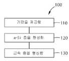
[0010]도 1은 본 개시내용의 하나 이상의 실시예에 따른 막 스택의 개략도를 도시한다.
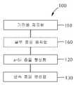
[0011]도 2a는 본 개시내용의 하나 이상의 실시예에 따른 프로세스 방식을 도시한다.
[0012]도 2b는, 도 2a의 프로세스 방식에 따른 막 스택의 개략도를 도시한다.
[0013]도 3은 본 개시내용의 하나 이상의 실시예에 따른 프로세스 방식을 도시한다.
[0014]도 4a는 본 개시내용의 하나 이상의 실시예에 따른 프로세스 방식을 도시한다.
[0015]도 4b는, 도 4a의 프로세스 방식에 따른 막 스택의 개략도를 도시한다.[0009] In the manner in which the recited features of the present disclosure can be understood in detail, a more particular description of the invention, briefly summarized above, may be had by reference to embodiments, some of which, Are illustrated in the accompanying drawings. It should be noted, however, that the appended drawings illustrate only typical embodiments of the present disclosure and, therefore, should not be construed as limiting the scope of the present disclosure, which is not intended to limit the scope of the present disclosure to other equally effective embodiments I can do it.
[0010] FIG. 1 illustrates a schematic diagram of a film stack according to one or more embodiments of the present disclosure.
[0011] FIG. 2a illustrates a process approach in accordance with one or more embodiments of the present disclosure.
[0012] FIG. 2B shows a schematic view of a film stack according to the process scheme of FIG. 2A.
[0013] FIG. 3 illustrates a process approach in accordance with one or more embodiments of the present disclosure.
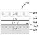
[0014] FIG. 4A illustrates a process approach in accordance with one or more embodiments of the present disclosure.
[0015] FIG. 4B shows a schematic view of a film stack according to the process scheme of FIG. 4A.
[0016]본 개시내용의 몇몇 예시적인 실시예들을 설명하기 전에, 본 개시내용은 하기의 설명에서 기술되는 구성 또는 프로세스 단계들의 세부사항들로 제한되지 않음이 이해되어야 한다. 본 개시내용은 다른 실시예들이 가능하며, 다양한 방식들로 실시되거나 수행될 수 있다.[0016]Before describing some exemplary embodiments of the present disclosure, it should be understood that this disclosure is not limited to the details of construction or process steps set forth in the following description. The present disclosure is capable of other embodiments and of being practiced or carried out in various ways.
[0017]본원에서 사용되는 바와 같은 "기판"은, 제조 프로세스 동안 막 프로세싱이 수행되는, 임의의 기판, 또는 기판 상에 형성된 재료 표면을 지칭한다. 예컨대, 프로세싱이 수행될 수 있는 기판 표면은, 애플리케이션에 의존하여, 실리콘, 실리콘 산화물, 스트레인드 실리콘(strained silicon), SOI(silicon on insulator), 탄소 도핑된 실리콘 산화물들, 비정질 실리콘, 도핑된 실리콘, 게르마늄, 갈륨 비소, 유리, 사파이어와 같은 재료들, 및 임의의 다른 재료들, 이를테면 금속들, 금속 질화물들, 금속 합금들, 및 다른 전도성 재료들을 포함한다. 기판들은, 비제한적으로 반도체 웨이퍼들을 포함한다. 기판들은, 기판 표면을 폴리싱(polish), 에칭, 환원, 산화, 히드록실화(hydroxylate), 어닐링(anneal) 및/또는 베이킹(bake)하기 위해 전처리 프로세스에 노출될 수 있다. 본 개시내용에서, 기판 자체의 표면 상에 직접적으로 막 프로세싱을 하는 것에 부가하여, 개시되는 막 프로세싱 단계들 중 임의의 막 프로세싱 단계는 또한, 아래에서 더 상세히 개시되는 바와 같이, 기판 상에 형성된 하부-층(under-layer) 상에서 수행될 수 있으며, "기판 표면"이라는 용어는 문맥이 표시하는 바에 따라 그러한 하부-층을 포함하도록 의도된다. 따라서, 예컨대, 막/층 또는 부분적인 막/층이 기판 표면 상에 증착된 경우, 새롭게 증착된 막/층의 노출된 표면이 기판 표면이 된다.[0017]A "substrate " as used herein refers to any substrate, or material surface formed on a substrate, during which the film processing is performed during the manufacturing process. For example, the substrate surface on which processing may be performed may be a silicon substrate, a silicon oxide, strained silicon, silicon on insulator (SOI), carbon doped silicon oxides, amorphous silicon, doped silicon , Germanium, gallium arsenide, glass, sapphire, and any other materials such as metals, metal nitrides, metal alloys, and other conductive materials. The substrates include, but are not limited to, semiconductor wafers. The substrates may be exposed to a pretreatment process to polish, etch, reduce, oxidize, hydroxylate, anneal and / or bake the substrate surface. In this disclosure, in addition to performing film processing directly on the surface of the substrate itself, any of the film processing steps of the disclosed film processing steps may also be performed on a substrate - the term "substrate surface" is intended to include such a sub-layer as the context indicates. Thus, for example, when a film / layer or a partial film / layer is deposited on a substrate surface, the exposed surface of the newly deposited film / layer becomes the substrate surface.
[0018]본 명세서 및 첨부된 청구항들에서 사용되는 바와 같이, "전구체", "반응물", "반응성 가스" 등과 같은 용어들은, 기판 표면과 반응할 수 있는 임의의 가스상 종(gaseous species)을 지칭하기 위해 상호교환가능하게 사용된다.[0018]As used herein and in the appended claims, terms such as "precursor "," reactant ", "reactive gas ", and the like refer to any gaseous species capable of reacting with a substrate surface. It is used interchangeably.
[0019]본 개시내용의 하나 이상의 실시예들은, 금속 ALD(예컨대, 텅스텐 증착)를 위한 글루 층, 불소 확산 배리어(diffusion barrier), 및/또는 핵형성 층 중 하나 이상으로서 컨포멀한(conformal) 비정질 실리콘 박막을 증착하는 방법들에 관한 것이다. 많은 실시예들에서 텅스텐 증착이 언급되지만, 당업자들은, 다른 금속들(예컨대, Mo)이 개시된 프로세스에 의해 증착될 수 있다는 것을 이해할 것이다. 본 개시내용은 ALD 텅스텐 증착으로 제한되지 않는다.[0019]One or more embodiments of the present disclosure provide a method of fabricating a conformal amorphous silicon thin film (e.g., a thin film) that is conformal as at least one of a glue layer for a metal ALD (e.g., tungsten deposition), a fluorine diffusion barrier, and / And the like. Although tungsten deposition is mentioned in many embodiments, those skilled in the art will appreciate that other metals (e.g., Mo) may be deposited by the disclosed process. This disclosure is not limited to ALD tungsten deposition.
[0020]본 개시내용의 실시예들은, 금속 ALD 프로세스들을 위한 프로세스 통합 방식들을 포함한다. 예컨대, 원자 층 증착에 의해 텅스텐이 실리콘 기판 상에 증착된다. 도 1을 참조하면, 스택(10)은, 글루 층(14)(예컨대, TiN), 핵형성 층(16)(예컨대, WSix 및 WBx), 및 금속(18)(예컨대, W)을 갖는 기판(12)(예컨대, SiO2)을 포함할 수 있다. 프로세스 방식의 하나 이상의 실시예에서, 핵형성 층은 비정질 실리콘 층으로 대체된다. 일부 실시예들에서, 핵형성 층은 비정질 실리콘 층으로 대체되고 그리고 TiN 글루 층은 더 얇게 만들어진다. 하나 이상의 실시예들에서, 핵형성 층 및 글루 층 둘 모두가 비정질 실리콘 층으로 대체된다.[0020] Embodiments of the present disclosure include process integration schemes for metal ALD processes. For example, tungsten is deposited on a silicon substrate by atomic layer deposition. Referring to Figure 1, the
[0021]도 2a 및 도 2b를 참조하면, 본 개시내용의 하나 이상의 실시예들은, 프로세싱 방법들(100) 및 막 스택들(200)에 관한 것이다. 단계(110)에서, 기판 표면(222)을 갖는 기판(220)이 제공된다. 단계(120)에서, 기판 표면(222) 상에 비정질 실리콘 층(240)을 형성하기 위해 기판(220)이 실리콘 전구체에 노출된다.[0021]Referring to Figures 2A and 2B, one or more embodiments of the present disclosure are directed to processing
[0022]일부 실시예들에서, 비정질 실리콘(a-Si) 형성은, 웨이퍼 온도를 최소화하면서 실리콘 전구체의 분압을 최대화함으로써 달성될 수 있다. 적절한 실리콘 전구체들은, 폴리-실란류(SixHy)를 포함하지만 이에 제한되지 않는다. 예컨대, 폴리-실란류는, 디실란(Si2H6), 트리실란(Si3H8), 테트라실란(Si4H10), 이소테트라실란, 네오펜타실란(Si5H12), 시클로펜타실란(Si5H10), 헥사실란(C6H14), 시클로헥사실란(Si6H12) 또는 일반적으로, x = 2 이상인 SixHy, 및 이들의 조합들을 포함한다. 예컨대, 중간의 프로세싱 온도 및 높은 증기압(vapor pressure)을 갖는 디실란이 단독으로 또는 다른 종과의 조합으로 실리콘 전구체로서 사용될 수 있다.[0022] In some embodiments, amorphous silicon (a-Si) formation can be achieved by maximizing the partial pressure of the silicon precursor while minimizing the wafer temperature. Suitable silicon precursors include, but are not limited to, poly-silanes (Six Hy ). For example, the poly-silanes may be selected from the group consisting of disilane (Si2 H6 ), trisilane (Si3 H8 ), tetrasilane (Si4 H10 ), isotetrasilane, neopentasilane (Si5 H12 ) Pentasilane (Si5 H10 ), hexasilane (C6 H14 ), cyclohexasilane (Si6 H12 ), or Six Hy , where x = 2 or more, and combinations thereof. For example, disilanes having intermediate processing temperatures and high vapor pressures can be used alone or in combination with other species as silicon precursors.
[0023]일부 실시예들에서, 실리콘 전구체는 실질적으로 디실란만을 포함한다. 본 명세서 및 첨부된 청구항들에서 사용되는 바와 같이, "실질적으로 디실란만"이라는 문구는 활성 종의 적어도 95 %가 디실란임을 의미한다. 캐리어 가스들 및 불활성 가스들과 같은 다른 가스들이 임의의 양으로 포함될 수 있다.[0023]In some embodiments, the silicon precursor substantially comprises only disilane. As used herein and in the appended claims, the phrase "substantially disilane only" means that at least 95% of the active species is disilane. Other gases such as carrier gases and inert gases may be included in any amount.
[0024]비정질 실리콘 층(240)의 두께는, 예컨대, 기판 표면 및 후속하는 막들 및 프로세스들에 따라 변할 수 있다. 일부 실시예들에서, 비정질 실리콘 층(240)은, 약 1 Å 내지 약 100 Å의 범위 내의 두께를 갖는다. 하나 이상의 실시예들에서, 비정질 실리콘 층(240)은, 약 1 Å 내지 약 50 Å의 범위, 또는 약 10 Å 내지 약 40 Å의 범위, 또는 약 30 Å내지 약 40 Å의 범위 내의 두께를 갖는다. 일부 실시예들에서, 비정질 실리콘 층(240)의 두께는, 0 Å보다 크고 약 50 Å, 45 Å, 또는 40 Å보다 작거나 같다.[0024]The thickness of the
[0025]단계(130)에서, 비정질 실리콘 층(240) 상에 금속 층(280)이 형성된다. 금속 층(280)은, 원자 층 증착(ALD), 플라즈마 강화 원자 층 증착(PE-ALD; plasma-enhanced atomic layer deposition), 화학 기상 증착(CVD; chemical vapor deposition), 플라즈마 강화 화학 기상 증착(PE-CVD; plasma-enhanced chemical vapor deposition), 및 물리 기상 증착(PVD; physical vapor deposition)을 포함하는(그러나 이들로 제한되지 않음) 임의의 적절한 기법에 의해 형성될 수 있다.[0025]In
[0026]금속 층(280)은 임의의 적절한 금속을 포함할 수 있다. 일부 실시예들에서, 금속 층(280)은, 텅스텐 또는 몰리브덴 중 하나 이상을 포함한다. 일부 실시예들에서, 금속 층(280)은, 본질적으로 텅스텐으로 이루어진다. 일부 실시예들에서, 금속 층(280)은, 본질적으로 몰리브덴으로 이루어진다. 이와 관련하여 사용되는 바와 같이, "본질적으로 ~로 이루어진다"는 것은, 금속 층(280)이 명시된 컴포넌트의 약 80, 85, 90, 또는 95 원자 %보다 크거나 같다는 것을 의미한다. 예컨대, 본질적으로 텅스텐으로 이루어진 금속 층(280)은, 예컨대, 약 90 원자 % 텅스텐보다 크거나 같은 조성을 갖는다.[0026]The
[0027]일부 실시예들에서, 금속 층(280)은 CVD에 의해 증착된다. 기판 상에 층을 증착하기 위해, 금속 전구체 및 반응물이 프로세싱 챔버 내로 공동유동(coflow)될 수 있다. 전구체 및 반응물은 가스 상(gas phase)에서 반응하도록 허용된다.[0027]In some embodiments, the
[0028]일부 실시예들에서, 금속 층(280)은 ALD에 의해 증착된다. 시간-도메인(time-domain) ALD 프로세스에서, 금속 전구체가 프로세싱 챔버 내로 유동되어 표면과 반응한다. 챔버에서 과잉 전구체 및 부산물(byproduct)들이 퍼지(purge)되고, 반응물이 챔버 내로 유동된다. 전구체와 반응물이 동시에 프로세싱 챔버 내에 있지 않으므로, 최소의 가스 상 반응들이 존재하거나 가스 상 반응들이 존재하지 않는다. 공간적(spatial) ALD 프로세스에서, 프로세싱 챔버의 제1 섹션(section) 내로 금속 전구체가 유동되고, 동시에 프로세싱 챔버의 제2 섹션 내로 반응물이 유동된다. 제1 섹션 및 제2 섹션은, 전구체와 반응물 간의 가스 상 반응들을 방지하기 위해 가스 커튼(gas curtain)에 의해 분리된다. 기판은 제1 섹션과 제2 섹션 사이에서 이동되어 전구체 및 반응물에 순차적으로 표면이 노출된다. 일부 실시예들에서, 금속 층(280)은, 비정질 실리콘 층(240)을 금속 전구체 및 반응물에 순차적으로 노출시킴으로써 증착된다.[0028]In some embodiments, the
[0029]금속 전구체는, 금속 막을 증착하는 데 사용될 수 있는 임의의 적절한 전구체일 수 있다. 일부 실시예들에서, 금속 전구체는, 텅스텐, 몰리브덴, 및 이들의 조합들로부터 선택되는 금속을 포함한다. 하나 이상의 실시예들에서, 금속 전구체는, WF6 및 MoF6 중 하나 이상을 포함한다. 일부 실시예들에서, 금속 전구체는 불소 함유 전구체이다. 불소는 실리콘 표면을 에칭할 수 있다는 것이 알려져 있다. 본 개시내용의 일부 실시예들은 유리하게 불소 전구체들의 사용을 허용하는데, 그 이유는, 전구체가 a-Si 막 전부를 제거하지는 않는다는 것을 보장하기에 충분한 두께로 비정질 실리콘 층(240)이 형성될 수 있기 때문이다.[0029] The metal precursor may be any suitable precursor that can be used to deposit the metal film. In some embodiments, the metal precursor comprises a metal selected from tungsten, molybdenum, and combinations thereof. In one or more embodiments, the metal precursor comprises at least one of WF6 and MoF6 . In some embodiments, the metal precursor is a fluorine containing precursor. It is known that fluorine can etch silicon surfaces. Some embodiments of the present disclosure advantageously permit the use of fluorine precursors because the
[0030]반응물은, 표면 상에 형성되는 종(species)과 반응할 수 있는 임의의 적절한 반응물일 수 있다. 예컨대, WF6이 전구체로서 사용되는 경우, -WFx 종이 표면 상에 존재할 것이다. 반응물은 -WFx 종과 반응하여 W 막을 생성할 수 있다.The reactants may be any suitable reactants capable of reacting with species formed on the surface. For example, if WF6 is used as a precursor, -WFx will be present on the paper surface. The reactants can react with -WFx species to produce a W film.
[0031]도 3은 본 개시내용의 다른 실시예에 대한 프로세스 흐름을 도시하며, 여기서, 비정질 실리콘 층(240)의 형성 이후에 탈기(degas) 프로세스(125)가 포함된다. 일부 실시예들에서, 금속 층(280)을 형성하기 전에, 아웃개싱된(outgassed) 종을 제거하기 위해, 비정질 실리콘 층(240)이 탈기 환경에 노출된다.[0031]FIG. 3 illustrates a process flow for another embodiment of the present disclosure, wherein a
[0032]증착된 비정질 실리콘 층(240)은 종(예컨대, 수소)을 방출 또는 아웃개싱할 수 있다. 탈기 환경은, 최종 막의 버블링(bubbling)을 최소화하면서 가스상 종이 방출될 기회를 제공한다. 탈기 환경은, 막의 탈기를 허용하거나 촉진시키는 임의의 조건을 포함할 수 있다. 예컨대, 탈기 환경은 본질적으로 불활성 가스로 이루어질 수 있다. 이와 관련하여 사용되는 바와 같이, "본질적으로 ~로 이루어진다"는 것은, 증착되는 막의 아웃개싱에 간섭하는 가스상 종이 존재하지 않음을 의미한다. 막의 탈기를 억제함이 없이 여전히 본질적으로 불활성 가스로 이루어지면서 다른 반응성 종이 존재할 수 있다.[0032]The deposited
[0033]적절한 불활성 가스들은 아르곤, 헬륨, 질소, 및/또는 이들의 혼합물들 중 하나 이상을 포함하지만 이들로 제한되지 않는다.[0033]Suitable inert gases include, but are not limited to, one or more of argon, helium, nitrogen, and / or mixtures thereof.
[0034]하나 이상의 실시예들에서, 아웃개싱된 종은, 수소, SiH2, SiH3, SiH4, 및/또는 다른 낮은-차수(low-order) 실란류를 포함한다.[0034] In one or more embodiments, the outgassed species include hydrogen, SiH2 , SiH3 , SiH4 , and / or other low-order silanes.
[0035]프로세싱 챔버 또는 프로세싱 챔버의 영역 내의 압력은, 전구체 노출 및 탈기 환경에 대해 독립적으로 제어될 수 있다. 일부 실시예들에서, 실리콘 전구체 및 탈기 환경 각각에 대한 노출은, 약 10 mTorr 내지 약 100 Torr의 범위 내의 압력에서 발생한다. 일부 실시예들에서, 실리콘 전구체는, 약 500 mTorr보다 크거나 같은 압력, 또는 약 1 Torr보다 크거나 같은 압력, 또는 약 5 Torr보다 크거나 같은 압력, 또는 약 10 Torr보다 크거나 같은 압력, 또는 약 20 Torr보다 크거나 같은 압력, 또는 약 30 Torr보다 크거나 같은 압력에서 기판에 노출된다.[0035]The pressure in the region of the processing chamber or processing chamber can be controlled independently for the precursor exposure and degassing environment. In some embodiments, the exposure to each of the silicon precursor and degassing environment occurs at a pressure in the range of about 10 mTorr to about 100 Torr. In some embodiments, the silicon precursor has a pressure greater than or equal to about 500 mTorr, or a pressure greater than or equal to about 1 Torr, or a pressure greater than or equal to about 5 Torr, or a pressure greater than or equal to about 10 Torr, A pressure greater than or equal to about 20 Torr, or a pressure greater than or equal to about 30 Torr.
[0036]기판 표면이 전구체 또는 탈기 환경에 노출되는 온도는, 예컨대, 형성되는 디바이스의 열 버짓(thermal budget) 및 전구체에 의존하여 변할 수 있다. 일부 실시예들에서, 전구체 및 탈기 환경 각각에 대한 노출은, 약 100 ℃ 내지 약 700 ℃의 범위 내의 온도에서 발생한다. 하나 이상의 실시예들에서, 약 250 ℃ 내지 약 600 ℃의 범위, 또는 약 400 ℃ 내지 약 550 ℃의 범위 내의 온도에서 실리콘 할로겐화물 전구체가 기판에 노출된다.[0036]The temperature at which the substrate surface is exposed to the precursor or degassing environment can vary depending on, for example, the thermal budget and the precursor of the device being formed. In some embodiments, the exposure to each of the precursor and degassing environment occurs at a temperature in the range of about 100 캜 to about 700 캜. In one or more embodiments, the silicon halide precursor is exposed to the substrate at a temperature in the range of about 250 ° C to about 600 ° C, or in the range of about 400 ° C to about 550 ° C.
[0037]탈기 환경에 대한 노출 전에 실리콘 전구체로 형성되는 a-Si 막의 두께는 변경될 수 있다. 일부 실시예들에서, 실리콘 전구체 및 탈기 환경에 대한 각각의 노출은, 약 5 Å 내지 약 20 Å의 범위 내의 두께를 갖는 막을 성장시킨다.[0037]The thickness of the a-Si film formed from the silicon precursor prior to exposure to the degassing environment can be varied. In some embodiments, each exposure to the silicon precursor and degassing environment grows a film having a thickness in the range of about 5 A to about 20 A.
[0038]전구체 및 탈기 환경들은, 미리결정된 두께를 갖는 막을 형성하기 위해, 반복적이고 순차적으로 기판 표면에 노출될 수 있다. 일부 실시예들에서, 비정질 실리콘 막은, 약 100 Å 내지 약 1 ㎛의 범위 내의 총 두께를 갖는다.[0038]Precursor and degassing environments can be exposed to the substrate surface repeatedly and sequentially to form a film having a predetermined thickness. In some embodiments, the amorphous silicon film has a total thickness in the range of about 100 A to about 1 mu m.
[0039]일부 실시예들에서, 약 450 ℃ 미만의 웨이퍼 온도에서 디실란에 의해 a-Si가 증착되고, 디실란 분압은 약 20 Torr보다 크거나 같다. 일 예시적인 실시예에서, 기판은, 약 400 ℃ 내지 약 550 ℃의 범위 내의 온도에서 그리고 약 20 Torr보다 크거나 같은 압력에서 실리콘 전구체에 노출된다.[0039]In some embodiments, a-Si is deposited by disilane at a wafer temperature of less than about 450 DEG C, and the disilane partial pressure is greater than or equal to about 20 Torr. In one exemplary embodiment, the substrate is exposed to the silicon precursor at a temperature within the range of about 400 [deg.] C to about 550 [deg.] C and at a pressure equal to or greater than about 20 Torr.
[0040]도 4a 및 도 4b를 참조하면, 본 개시내용의 일부 실시예들은 단계(160)를 더 포함하며, 이 단계에서, 비정질 실리콘 층(240)을 형성하기 전에 글루 층(260)이 기판 상에 증착된다. 글루 층(260)은, 비정질 실리콘 층이 기판(220) 상에 직접 증착되었을 경우보다 적은 박리(peeling) 가능성으로 비정질 실리콘이 점착될 수 있는 층이다. 일부 실시예들에서, 글루 층은 TiN을 포함한다. 하나 이상의 실시예들에서, 기판(220)은 실리콘 산화물 표면을 갖고, 글루 층은 TiN을 포함한다.[0040]4A and 4B, some embodiments of the present disclosure further include a
[0041]글루 층(260)의 두께는, 기판, 및 증착될 비정질 실리콘의 두께에 따라 변할 수 있다. 일부 실시예들에서, 글루 층(260)은, 약 1 Å 내지 약 30 Å의 범위, 또는 약 5 Å 내지 약 30 Å의 범위 내의 두께를 갖는다. 일부 실시예들에서, 글루 층(260)은, 약 20 Å보다 작거나 같은 두께, 또는 약 15 Å보다 작거나 같은 두께, 또는 약 10 Å보다 작거나 같은 두께, 또는 약 5 Å보다 작거나 같은 두께를 갖는다.[0041]The thickness of the
[0042]도 4b를 참조하면, 본 개시내용의 하나 이상의 실시예들은, 산화물 표면(222)을 갖는 기판(220)을 포함하는 스택들(200)에 관한 것이다. 산화물 표면(222) 상에 글루 층(260)이 있다. 일부 실시예들의 글루 층은, 약 5 Å 내지 약 30 Å의 범위 내의 두께를 갖는 TiN을 포함한다. 글루 층(260) 상에 비정질 실리콘 층(240)이 있으며, 비정질 실리콘 층(240)은, 약 5 Å 내지 약 50 Å의 범위 내의 두께를 갖는다. 비정질 실리콘 층(240) 상에 금속 층(280)이 있으며, 금속 층(280)은, 텅스텐 및 몰리브덴 중 하나 이상을 포함한다.[0042]Referring to FIG. 4B, one or more embodiments of the present disclosure are directed to
[0043]하나 이상의 실시예들에 따르면, 기판은, 층을 형성하기 전에 그리고/또는 층을 형성한 후에, 프로세싱을 겪는다. 이러한 프로세싱은, 동일한 챔버에서 또는 하나 이상의 별개의 프로세싱 챔버들에서 수행될 수 있다. 일부 실시예들에서, 기판은, 추가적인 프로세싱을 위해, 제1 챔버로부터 별개의 제2 챔버로 이동된다. 기판은, 제1 챔버로부터 별개의 프로세싱 챔버로 직접적으로 이동될 수 있거나, 또는 기판은, 제1 챔버로부터 하나 이상의 이송 챔버들로 이동될 수 있고, 그 후에, 별개의 프로세싱 챔버로 이동될 수 있다. 따라서, 프로세싱 장치는 이송 스테이션과 통신하는 다수의 챔버들을 포함할 수 있다. 이러한 종류의 장치는 "클러스터 툴(cluster tool)" 또는 "클러스터형 시스템" 등으로 지칭될 수 있다.[0043]According to one or more embodiments, the substrate undergoes processing before forming the layer and / or after forming the layer. Such processing may be performed in the same chamber or in one or more separate processing chambers. In some embodiments, the substrate is moved from the first chamber to a separate second chamber for further processing. The substrate can be moved directly from the first chamber to a separate processing chamber or the substrate can be moved from the first chamber to one or more transfer chambers and then moved to a separate processing chamber . Thus, the processing device may include a plurality of chambers in communication with the transfer station. Devices of this kind may be referred to as "cluster tools" or "clustered systems ".
[0044]일반적으로, 클러스터 툴은, 기판 중심-발견 및 배향, 탈기, 어닐링, 증착, 및/또는 에칭을 포함하는 다양한 기능들을 수행하는 다수의 챔버들을 포함하는 모듈러(modular) 시스템이다. 하나 이상의 실시예들에 따르면, 클러스터 툴은, 적어도 제1 챔버 및 중앙 이송 챔버를 포함한다. 중앙 이송 챔버는, 로드 록 챔버들과 프로세싱 챔버들 사이에서 그리고 이들 간에서 기판들을 셔틀링(shuttle)할 수 있는 로봇을 하우징(house)할 수 있다. 이송 챔버는 통상적으로, 진공 조건에서 유지되고, 기판들을, 하나의 챔버로부터 다른 챔버로, 그리고/또는 클러스터 툴의 전방 단부에 포지셔닝된(positioned) 로드 록 챔버로 셔틀링하기 위한 중간 스테이지를 제공한다. 본 개시내용에 대해 적응될 수 있는 2개의 잘-알려진 클러스터 툴들은 Centura® 및 Endura®이고, 이들 둘 모두는, 캘리포니아 주 Santa Clara의 Applied Materials, Inc.로부터 입수가능하다. 하지만, 챔버들의 정확한 어레인지먼트 및 조합은, 본원에서 설명되는 바와 같은 프로세스의 특정 단계들을 수행하는 목적들을 위해 변경될 수 있다. 사용될 수 있는 다른 프로세싱 챔버들은, 주기적 층 증착(CLD; cyclical layer deposition), 원자 층 증착(ALD), 화학 기상 증착(CVD), 물리 기상 증착(PVD), 에칭, 사전-세정, 화학 세정, RTP와 같은 열 처리, 플라즈마 질화(nitridation), 탈기, 배향, 히드록실화(hydroxylation), 및 다른 기판 프로세스들을 포함하지만 이들로 제한되지 않는다. 클러스터 툴 상의 챔버에서 프로세스들을 수행함으로써, 대기 불순물들에 의한 기판의 표면 오염이, 후속 막을 증착하기 전의 산화 없이, 회피될 수 있다.[0044] In general, the cluster tool is a modular system that includes a number of chambers that perform various functions including substrate center-finding and orientation, degassing, annealing, deposition, and / or etching. According to one or more embodiments, the cluster tool comprises at least a first chamber and a central transfer chamber. The central transfer chamber may house a robot capable of shuttling the substrates between and between the load lock chambers and the processing chambers. The transfer chamber is typically maintained in a vacuum condition and provides an intermediate stage for shuttling the substrates from one chamber to another and / or to a load lock chamber positioned at the front end of the cluster tool . Two well that may be adapted to the present disclosure - and the known cluster tools Centura® and Endura®, both of which are available from, of California Santa Clara Applied Materials, Inc.. However, the precise arrangement and combination of chambers may be modified for purposes of performing certain steps of the process as described herein. Other processing chambers that may be used include, but are not limited to, cyclical layer deposition (CLD), atomic layer deposition (ALD), chemical vapor deposition (CVD), physical vapor deposition (PVD), etching, pre- But are not limited to, thermal processing such as plasma treatment, plasma nitridation, degassing, orientation, hydroxylation, and other substrate processes. By performing processes in a chamber on a cluster tool, surface contamination of the substrate by atmospheric impurities can be avoided without oxidation prior to deposition of the subsequent film.
[0045]하나 이상의 실시예들에 따르면, 기판은 지속적으로 진공 또는 "로드 록" 조건들 하에 있고, 하나의 챔버로부터 다음 챔버로 이동될 때, 주변 공기에 노출되지 않는다. 따라서, 이송 챔버들은 진공 하에 있고, 진공 압력 하에서 "펌핑 다운(pump down)"된다. 불활성 가스들이 프로세싱 챔버들 또는 이송 챔버들에 존재할 수 있다. 일부 실시예들에서, 불활성 가스는, 반응물들의 일부 또는 전부를 제거하기 위해, 퍼지 가스로서 사용된다. 하나 이상의 실시예들에 따르면, 퍼지 가스는, 반응물들이 증착 챔버로부터 이송 챔버로 그리고/또는 부가적인 프로세싱 챔버로 이동하는 것을 방지하기 위해, 증착 챔버의 출구에서 주입된다. 따라서, 불활성 가스의 유동은 챔버의 출구에서 커튼을 형성한다.[0045]According to one or more embodiments, the substrate is under constant vacuum or "load lock" conditions and is not exposed to ambient air when moved from one chamber to the next. Thus, the transfer chambers are under vacuum and are "pumped down" under vacuum pressure. Inert gases may be present in the processing chambers or transfer chambers. In some embodiments, the inert gas is used as a purge gas to remove some or all of the reactants. According to one or more embodiments, the purge gas is injected at the outlet of the deposition chamber to prevent reactants from moving from the deposition chamber to the transfer chamber and / or to the additional processing chamber. Thus, the flow of the inert gas forms a curtain at the outlet of the chamber.
[0046]기판은, 단일 기판이 로딩되고, 프로세싱되고, 그리고 다른 기판이 프로세싱되기 전에 언로딩되는, 단일 기판 증착 챔버들에서 프로세싱될 수 있다. 기판은 또한, 다수의 기판이 챔버의 제1 부분 내로 개별적으로 로딩되고, 챔버를 통해 이동하고, 그리고 챔버의 제2 부분으로부터 언로딩되는, 컨베이어 시스템과 유사하게, 연속적인 방식으로 프로세싱될 수 있다. 챔버 및 연관된 컨베이어 시스템의 형상은 직선 경로 또는 곡선 경로를 형성할 수 있다. 부가적으로, 프로세싱 챔버는, 다수의 기판들이 중심 축을 중심으로 이동되고 그리고 캐러셀(carousel) 경로 전반에 걸쳐 증착, 에칭, 어닐링, 세정 등의 프로세스들에 노출되는 캐러셀일 수 있다.[0046]The substrate may be processed in a single substrate deposition chamber, where a single substrate is loaded, processed, and unloaded before the other substrate is processed. The substrate can also be processed in a continuous manner, similar to a conveyor system in which a plurality of substrates are individually loaded into a first portion of a chamber, moved through a chamber, and unloaded from a second portion of the chamber . The shape of the chamber and associated conveyor system may form a straight or curved path. Additionally, the processing chamber may be a carousel in which a plurality of substrates are moved about a central axis and exposed to processes such as deposition, etching, annealing, cleaning, etc. throughout the carousel path.
[0047]프로세싱 동안, 기판은 가열 또는 냉각될 수 있다. 그러한 가열 또는 냉각은, 기판 지지부의 온도를 변화시키는 것 및 가열된 또는 냉각된 가스들을 기판 표면으로 유동시키는 것을 포함하는(그러나 이에 제한되지 않음) 임의의 적절한 수단에 의해 달성될 수 있다. 일부 실시예들에서, 기판 지지부는, 기판 온도를 전도식으로(conductively) 변화시키도록 제어될 수 있는 가열기/냉각기를 포함한다. 하나 이상의 실시예들에서, 이용되는 가스들(반응성 가스들 또는 불활성 가스들)은, 기판 온도를 국부적으로 변화시키도록 가열 또는 냉각된다. 일부 실시예들에서, 가열기/냉각기는, 기판 온도를 대류식으로(convectively) 변화시키기 위해, 챔버 내에서 기판 표면에 인접하게 포지셔닝된다.[0047]During processing, the substrate may be heated or cooled. Such heating or cooling may be accomplished by any suitable means including, but not limited to, changing the temperature of the substrate support and flowing heated or cooled gases to the substrate surface. In some embodiments, the substrate support includes a heater / cooler that can be controlled to conductively vary the substrate temperature. In one or more embodiments, the gases used (reactive gases or inert gases) are heated or cooled to locally vary the substrate temperature. In some embodiments, the heater / cooler is positioned adjacent to the substrate surface within the chamber to convectively vary the substrate temperature.
[0048]기판은 또한, 프로세싱 동안, 고정식일 수 있거나 또는 회전될 수 있다. 회전되는 기판은, 연속적으로 또는 불연속적인 단계들로 회전될 수 있다. 예컨대, 기판은 전체 프로세스 전반에 걸쳐 회전될 수 있거나, 또는 기판은, 상이한 반응성 또는 퍼지 가스들에 대한 노출들 사이에서 작은 양만큼 회전될 수 있다. (연속적으로 또는 단계들로) 프로세싱 동안 기판을 회전시키는 것은, 예컨대, 가스 유동 기하학적 구조들에서의 국부적인 변동성의 영향을 최소화함으로써, 더 균일한 증착 또는 에칭을 생성하는 것을 도울 수 있다.[0048]The substrate may also be stationary or rotated during processing. The substrate to be rotated can be rotated in successive or discontinuous steps. For example, the substrate may be rotated throughout the entire process, or the substrate may be rotated by a small amount between exposures to different reactive or purge gases. Rotating the substrate during processing (successively or in steps) may help to produce a more uniform deposition or etch, for example, by minimizing the effect of local variations in gas flow geometries.
[0049]원자 층 증착 타입 챔버들에서, 기판은, 공간적으로 또는 시간적으로 분리된 프로세스들에서 제1 및 제2 전구체들에 노출될 수 있다. 시간적(temporal) ALD는, 제1 전구체가 챔버 내로 유동하여 표면과 반응하는 전통적인 프로세스이다. 제2 전구체를 유동시키기 전에, 제1 전구체가 챔버로부터 퍼지된다. 공간적 ALD에서, 제1 및 제2 전구체들 둘 모두가 동시에 챔버로 유동되지만, 전구체들의 혼합을 방지하는 영역이 유동들 사이에 존재하도록 공간적으로 분리된다. 공간적 ALD에서, 기판이 가스 분배 플레이트에 대해 이동되거나, 또는 그 반대도 가능하다.[0049]In atomic layer deposition type chambers, the substrate may be exposed to the first and second precursors in spatially or temporally separate processes. Temporal ALD is a traditional process in which the first precursor flows into the chamber and reacts with the surface. Before flowing the second precursor, the first precursor is purged from the chamber. In spatial ALD, both the first and second precursors flow into the chamber simultaneously, but spatially separate so that an area that prevents mixing of the precursors is between the flows. In spatial ALD, the substrate may be moved relative to the gas distribution plate, or vice versa.
[0050]방법들의 부분들 중 하나 이상이 하나의 챔버에서 발생하는 실시예들에서, 프로세스는 공간적 ALD 프로세스일 수 있다. 위에서 설명된 화학물들 중 하나 이상이 호환가능하지 않을 수 있지만(즉, 챔버 상에서의 증착 및/또는 기판 표면 상에서가 아닌 반응을 초래함), 공간적 분리는 시약들이 가스 상에서 서로에 노출되지 않는다는 것을 보장한다. 예컨대, 시간적 ALD는 증착 챔버를 퍼지하는 것을 수반한다. 그러나, 실제로, 추가의 시약을 유동시키기 전에 과잉 시약을 챔버로부터 퍼지하는 것은 때때로 불가능하다. 따라서, 챔버 내의 임의의 남아있는 시약이 반응할 수 있다. 공간적 분리를 이용하면, 과잉 시약이 퍼지될 필요가 없으며, 교차-오염이 제한된다. 또한, 챔버를 퍼지하기 위해서는 많은 시간이 사용될 수 있으며, 따라서, 퍼지 단계를 제거함으로써 스루풋이 증가될 수 있다.[0050]In embodiments in which one or more of the portions of the methods occur in one chamber, the process may be a spatial ALD process. While one or more of the chemistries described above may not be compatible (i.e., result in deposition on the chamber and / or reaction not on the substrate surface), spatial separation ensures that the reagents are not exposed to each other in the gas do. For example, temporal ALD involves purging the deposition chamber. However, in practice, it is sometimes impossible to purge the excess reagent from the chamber before flowing the additional reagent. Thus, any remaining reagent in the chamber can react. With spatial separation, the excess reagent does not need to be purged and cross-contamination is limited. Also, a large amount of time can be used to purge the chamber, and therefore throughput can be increased by eliminating the purge step.
[0051]본 명세서 전반에 걸쳐 "일 실시예", "특정 실시예들", "하나 이상의 실시예들" 또는 "실시예"에 대한 언급은, 실시예와 관련하여 설명되는 특정 피쳐, 구조, 재료, 또는 특징이 본 개시내용의 적어도 하나의 실시예에 포함된다는 것을 의미한다. 따라서, 본 명세서 전반에 걸쳐 다양한 위치들에서의 "하나 이상의 실시예들에서", "특정 실시예들에서", "일 실시예에서" 또는 "실시예에서"와 같은 문구들의 출현들은 반드시 본 개시내용의 동일한 실시예를 지칭하는 것은 아니다. 또한, 특정 피쳐들, 구조들, 재료들, 또는 특징들은 하나 이상의 실시예들에서 임의의 적절한 방식으로 조합될 수 있다.[0051]Reference throughout this specification to "one embodiment," " certain embodiments, "" one or more embodiments," or "an embodiment" means that a particular feature, And that the features are included in at least one embodiment of the present disclosure. Thus, the appearances of the phrases "in one or more embodiments," in certain embodiments, "in one embodiment," or "in an embodiment," But not to the same embodiment of the content. In addition, certain features, structures, materials, or features may be combined in any suitable manner in one or more embodiments.
[0052]본원에서의 개시내용이 특정 실시예들을 참조하여 설명되었지만, 이러한 실시예들은 단지 본 개시내용의 원리들 및 애플리케이션들을 예시하는 것임이 이해되어야 한다. 본 개시내용의 사상 및 범위를 벗어나지 않으면서 본 개시내용의 방법 및 장치에 대해 다양한 수정들 및 변형들이 이루어질 수 있음이 당업자에게 자명할 것이다. 따라서, 본 개시내용은 첨부된 청구항들 및 그 등가물들의 범위 내에 있는 수정들 및 변형들을 포함하는 것으로 의도된다.[0052]While the disclosure herein has been described with reference to particular embodiments, it should be understood that these embodiments are merely illustrative of the principles and applications of the present disclosure. It will be apparent to those skilled in the art that various modifications and variations can be made in the method and apparatus of the present disclosure without departing from the spirit and scope of the disclosure. It is therefore intended that the present disclosure cover all such modifications and variations as fall within the scope of the appended claims and their equivalents.
Claims (15)
Translated fromKorean두께를 갖는 비정질(amorphous) 실리콘 층을 형성하기 위해 기판 표면을 실리콘 전구체(precursor)에 노출시키는 단계; 및
상기 비정질 실리콘 층 상에 금속 층을 형성하는 단계를 포함하는, 프로세싱 방법.As a processing method,
Exposing the substrate surface to a silicon precursor to form an amorphous silicon layer having a thickness; And
And forming a metal layer on the amorphous silicon layer.
상기 실리콘 전구체는 폴리-실란을 포함하는, 프로세싱 방법.The method according to claim 1,
Wherein the silicon precursor comprises poly-silane.
상기 폴리-실란은, 디실란, 트리실란, 테트라실란, 이소테트라실란, 네오펜타실란, 시클로펜타실란, 헥사실란, 또는 시클로헥사실란 중 하나 이상을 포함하는, 프로세싱 방법.3. The method of claim 2,
Wherein the poly-silane comprises at least one of disilane, trisilane, tetrasilane, isotetrasilane, neopentasilane, cyclopentasilane, hexasilane, or cyclohexasilane.
상기 실리콘 전구체는 실질적으로 디실란만을 포함하는, 프로세싱 방법.3. The method of claim 2,
Wherein the silicon precursor substantially comprises only disilane.
상기 금속 층을 형성하는 단계 전에, 아웃개싱된 종(outgassed species)을 제거하기 위해 상기 비정질 실리콘 층을 탈기(degas) 환경에 노출시키는 단계를 더 포함하는, 프로세싱 방법.5. The method according to any one of claims 1 to 4,
Further comprising exposing the amorphous silicon layer to a degassing environment to remove outgassed species prior to forming the metal layer.
상기 탈기 환경은 본질적으로 불활성 가스로 이루어지는, 프로세싱 방법.6. The method of claim 5,
Wherein the degassing environment consists essentially of an inert gas.
상기 불활성 가스는, 아르곤, 헬륨, 및 질소 중 하나 이상을 포함하는, 프로세싱 방법.The method according to claim 6,
Wherein the inert gas comprises at least one of argon, helium, and nitrogen.
상기 비정질 실리콘 층의 두께는, 약 1 Å 내지 약 100 Å의 범위 내에 있는, 프로세싱 방법.5. The method according to any one of claims 1 to 4,
Wherein the thickness of the amorphous silicon layer is in the range of about 1 A to about 100 A.
상기 비정질 실리콘 층을 형성하기 전에 상기 기판 상에 글루(glue) 층을 증착하는 단계를 더 포함하는, 프로세싱 방법.5. The method according to any one of claims 1 to 4,
Further comprising depositing a glue layer on the substrate prior to forming the amorphous silicon layer.
상기 글루 층은 TiN을 포함하는, 프로세싱 방법.10. The method of claim 9,
Wherein the glue layer comprises TiN.
상기 기판 표면은 실리콘 산화물을 포함하는, 프로세싱 방법.11. The method of claim 10,
Wherein the substrate surface comprises silicon oxide.
TiN 층은 약 5 Å 내지 약 30 Å의 범위 내의 두께를 갖고 그리고 상기 비정질 실리콘 층은 약 5 Å 내지 약 50 Å의 범위 내의 두께를 갖는, 프로세싱 방법.12. The method of claim 11,
TiN layer has a thickness in the range of about 5 A to about 30 A and the amorphous silicon layer has a thickness in the range of about 5 A to about 50 A.
상기 금속 층은, 텅스텐 및 몰리브덴 중 하나 이상을 포함하는, 프로세싱 방법.5. The method according to any one of claims 1 to 4,
Wherein the metal layer comprises at least one of tungsten and molybdenum.
상기 금속 층은, 상기 비정질 실리콘 층을 금속 전구체 및 반응물에 순차적으로 노출시킴으로써 증착되고, 상기 금속 전구체는 WF6 및 MoF6 중 하나 이상을 포함하고, 그리고 상기 반응물은 수소를 포함하는, 프로세싱 방법.14. The method of claim 13,
Wherein the metal layer is deposited by sequentially exposing the amorphous silicon layer to a metal precursor and a reactant, wherein the metal precursor comprises at least one of WF6 and MoF6 , and wherein the reactant comprises hydrogen.
산화물 표면을 갖는 기판;
상기 산화물 표면 상의 글루 층 ― 상기 글루 층은, 약 5 Å 내지 약 30 Å의 범위 내의 두께를 갖는 TiN을 포함함 ―;
상기 글루 층 상의 비정질 실리콘 층 ― 상기 비정질 실리콘 층은, 약 5 Å 내지 약 50 Å의 범위 내의 두께를 가짐 ―; 및
상기 비정질 실리콘 층 상의 금속 층을 포함하며,
상기 금속 층은, 텅스텐 및 몰리브덴 중 하나 이상을 포함하는, 스택.As a stack,
A substrate having an oxide surface;
A glue layer on the oxide surface, the glue layer comprising TiN having a thickness in the range of about 5 A to about 30 A;
The amorphous silicon layer on the glue layer, the amorphous silicon layer having a thickness in the range of about 5 A to about 50 A; And
And a metal layer on the amorphous silicon layer,
Wherein the metal layer comprises at least one of tungsten and molybdenum.
Priority Applications (1)
| Application Number | Priority Date | Filing Date | Title |
|---|---|---|---|
| KR1020257002397AKR102866666B1 (en) | 2015-12-19 | 2016-12-16 | Conformal amorphous silicon as nucleation layer for w ald process |
Applications Claiming Priority (3)
| Application Number | Priority Date | Filing Date | Title |
|---|---|---|---|
| US201562269974P | 2015-12-19 | 2015-12-19 | |
| US62/269,974 | 2015-12-19 | ||
| PCT/US2016/067204WO2017106660A1 (en) | 2015-12-19 | 2016-12-16 | Conformal amorphous silicon as nucleation layer for w ald process |
Related Child Applications (1)
| Application Number | Title | Priority Date | Filing Date |
|---|---|---|---|
| KR1020257002397ADivisionKR102866666B1 (en) | 2015-12-19 | 2016-12-16 | Conformal amorphous silicon as nucleation layer for w ald process |
Publications (1)
| Publication Number | Publication Date |
|---|---|
| KR20180087441Atrue KR20180087441A (en) | 2018-08-01 |
Family
ID=59057786
Family Applications (2)
| Application Number | Title | Priority Date | Filing Date |
|---|---|---|---|
| KR1020257002397AActiveKR102866666B1 (en) | 2015-12-19 | 2016-12-16 | Conformal amorphous silicon as nucleation layer for w ald process |
| KR1020187020543ACeasedKR20180087441A (en) | 2015-12-19 | 2016-12-16 | Conformal amorphous silicon < RTI ID = 0.0 > |
Family Applications Before (1)
| Application Number | Title | Priority Date | Filing Date |
|---|---|---|---|
| KR1020257002397AActiveKR102866666B1 (en) | 2015-12-19 | 2016-12-16 | Conformal amorphous silicon as nucleation layer for w ald process |
Country Status (5)
| Country | Link |
|---|---|
| US (1) | US9978685B2 (en) |
| KR (2) | KR102866666B1 (en) |
| CN (1) | CN108369897B (en) |
| TW (1) | TWI716511B (en) |
| WO (1) | WO2017106660A1 (en) |
Cited By (2)
| Publication number | Priority date | Publication date | Assignee | Title |
|---|---|---|---|---|
| KR20190100859A (en)* | 2018-02-21 | 2019-08-29 | 도쿄엘렉트론가부시키가이샤 | Tungsten film-forming method, film-forming system and storage medium |
| KR20210069731A (en)* | 2018-10-29 | 2021-06-11 | 어플라이드 머티어리얼스, 인코포레이티드 | continuous linerless amorphous metal films |
Families Citing this family (286)
| Publication number | Priority date | Publication date | Assignee | Title |
|---|---|---|---|---|
| US20130023129A1 (en) | 2011-07-20 | 2013-01-24 | Asm America, Inc. | Pressure transmitter for a semiconductor processing environment |
| US10714315B2 (en) | 2012-10-12 | 2020-07-14 | Asm Ip Holdings B.V. | Semiconductor reaction chamber showerhead |
| US20160376700A1 (en) | 2013-02-01 | 2016-12-29 | Asm Ip Holding B.V. | System for treatment of deposition reactor |
| US11015245B2 (en) | 2014-03-19 | 2021-05-25 | Asm Ip Holding B.V. | Gas-phase reactor and system having exhaust plenum and components thereof |
| US10941490B2 (en) | 2014-10-07 | 2021-03-09 | Asm Ip Holding B.V. | Multiple temperature range susceptor, assembly, reactor and system including the susceptor, and methods of using the same |
| US10276355B2 (en) | 2015-03-12 | 2019-04-30 | Asm Ip Holding B.V. | Multi-zone reactor, system including the reactor, and method of using the same |
| US10458018B2 (en) | 2015-06-26 | 2019-10-29 | Asm Ip Holding B.V. | Structures including metal carbide material, devices including the structures, and methods of forming same |
| US10211308B2 (en) | 2015-10-21 | 2019-02-19 | Asm Ip Holding B.V. | NbMC layers |
| US10480066B2 (en) | 2015-12-19 | 2019-11-19 | Applied Materials, Inc. | Metal deposition methods |
| US10991586B2 (en) | 2015-12-19 | 2021-04-27 | Applied Materials, Inc. | In-situ tungsten deposition without barrier layer |
| US10468263B2 (en) | 2015-12-19 | 2019-11-05 | Applied Materials, Inc. | Tungsten deposition without barrier layer |
| US11139308B2 (en) | 2015-12-29 | 2021-10-05 | Asm Ip Holding B.V. | Atomic layer deposition of III-V compounds to form V-NAND devices |
| US10529554B2 (en) | 2016-02-19 | 2020-01-07 | Asm Ip Holding B.V. | Method for forming silicon nitride film selectively on sidewalls or flat surfaces of trenches |
| US10343920B2 (en) | 2016-03-18 | 2019-07-09 | Asm Ip Holding B.V. | Aligned carbon nanotubes |
| US10367080B2 (en) | 2016-05-02 | 2019-07-30 | Asm Ip Holding B.V. | Method of forming a germanium oxynitride film |
| US11453943B2 (en) | 2016-05-25 | 2022-09-27 | Asm Ip Holding B.V. | Method for forming carbon-containing silicon/metal oxide or nitride film by ALD using silicon precursor and hydrocarbon precursor |
| US9859151B1 (en) | 2016-07-08 | 2018-01-02 | Asm Ip Holding B.V. | Selective film deposition method to form air gaps |
| US10612137B2 (en) | 2016-07-08 | 2020-04-07 | Asm Ip Holdings B.V. | Organic reactants for atomic layer deposition |
| US9812320B1 (en) | 2016-07-28 | 2017-11-07 | Asm Ip Holding B.V. | Method and apparatus for filling a gap |
| KR102532607B1 (en) | 2016-07-28 | 2023-05-15 | 에이에스엠 아이피 홀딩 비.브이. | Substrate processing apparatus and method of operating the same |
| US9887082B1 (en) | 2016-07-28 | 2018-02-06 | Asm Ip Holding B.V. | Method and apparatus for filling a gap |
| US11532757B2 (en) | 2016-10-27 | 2022-12-20 | Asm Ip Holding B.V. | Deposition of charge trapping layers |
| US10714350B2 (en) | 2016-11-01 | 2020-07-14 | ASM IP Holdings, B.V. | Methods for forming a transition metal niobium nitride film on a substrate by atomic layer deposition and related semiconductor device structures |
| KR102546317B1 (en) | 2016-11-15 | 2023-06-21 | 에이에스엠 아이피 홀딩 비.브이. | Gas supply unit and substrate processing apparatus including the same |
| KR102762543B1 (en) | 2016-12-14 | 2025-02-05 | 에이에스엠 아이피 홀딩 비.브이. | Substrate processing apparatus |
| US11447861B2 (en) | 2016-12-15 | 2022-09-20 | Asm Ip Holding B.V. | Sequential infiltration synthesis apparatus and a method of forming a patterned structure |
| US11581186B2 (en) | 2016-12-15 | 2023-02-14 | Asm Ip Holding B.V. | Sequential infiltration synthesis apparatus |
| KR102700194B1 (en) | 2016-12-19 | 2024-08-28 | 에이에스엠 아이피 홀딩 비.브이. | Substrate processing apparatus |
| US10269558B2 (en) | 2016-12-22 | 2019-04-23 | Asm Ip Holding B.V. | Method of forming a structure on a substrate |
| US10867788B2 (en)* | 2016-12-28 | 2020-12-15 | Asm Ip Holding B.V. | Method of forming a structure on a substrate |
| US11390950B2 (en) | 2017-01-10 | 2022-07-19 | Asm Ip Holding B.V. | Reactor system and method to reduce residue buildup during a film deposition process |
| US10468261B2 (en) | 2017-02-15 | 2019-11-05 | Asm Ip Holding B.V. | Methods for forming a metallic film on a substrate by cyclical deposition and related semiconductor device structures |
| US10529563B2 (en) | 2017-03-29 | 2020-01-07 | Asm Ip Holdings B.V. | Method for forming doped metal oxide films on a substrate by cyclical deposition and related semiconductor device structures |
| US10770286B2 (en) | 2017-05-08 | 2020-09-08 | Asm Ip Holdings B.V. | Methods for selectively forming a silicon nitride film on a substrate and related semiconductor device structures |
| US12040200B2 (en) | 2017-06-20 | 2024-07-16 | Asm Ip Holding B.V. | Semiconductor processing apparatus and methods for calibrating a semiconductor processing apparatus |
| US11306395B2 (en) | 2017-06-28 | 2022-04-19 | Asm Ip Holding B.V. | Methods for depositing a transition metal nitride film on a substrate by atomic layer deposition and related deposition apparatus |
| KR20190009245A (en) | 2017-07-18 | 2019-01-28 | 에이에스엠 아이피 홀딩 비.브이. | Methods for forming a semiconductor device structure and related semiconductor device structures |
| US10541333B2 (en) | 2017-07-19 | 2020-01-21 | Asm Ip Holding B.V. | Method for depositing a group IV semiconductor and related semiconductor device structures |
| US11374112B2 (en) | 2017-07-19 | 2022-06-28 | Asm Ip Holding B.V. | Method for depositing a group IV semiconductor and related semiconductor device structures |
| US11018002B2 (en) | 2017-07-19 | 2021-05-25 | Asm Ip Holding B.V. | Method for selectively depositing a Group IV semiconductor and related semiconductor device structures |
| US10590535B2 (en) | 2017-07-26 | 2020-03-17 | Asm Ip Holdings B.V. | Chemical treatment, deposition and/or infiltration apparatus and method for using the same |
| TWI815813B (en) | 2017-08-04 | 2023-09-21 | 荷蘭商Asm智慧財產控股公司 | Showerhead assembly for distributing a gas within a reaction chamber |
| US10692741B2 (en) | 2017-08-08 | 2020-06-23 | Asm Ip Holdings B.V. | Radiation shield |
| US10770336B2 (en) | 2017-08-08 | 2020-09-08 | Asm Ip Holding B.V. | Substrate lift mechanism and reactor including same |
| US11769682B2 (en) | 2017-08-09 | 2023-09-26 | Asm Ip Holding B.V. | Storage apparatus for storing cassettes for substrates and processing apparatus equipped therewith |
| US11139191B2 (en) | 2017-08-09 | 2021-10-05 | Asm Ip Holding B.V. | Storage apparatus for storing cassettes for substrates and processing apparatus equipped therewith |
| US11830730B2 (en) | 2017-08-29 | 2023-11-28 | Asm Ip Holding B.V. | Layer forming method and apparatus |
| KR102491945B1 (en) | 2017-08-30 | 2023-01-26 | 에이에스엠 아이피 홀딩 비.브이. | Substrate processing apparatus |
| US11295980B2 (en) | 2017-08-30 | 2022-04-05 | Asm Ip Holding B.V. | Methods for depositing a molybdenum metal film over a dielectric surface of a substrate by a cyclical deposition process and related semiconductor device structures |
| US11056344B2 (en) | 2017-08-30 | 2021-07-06 | Asm Ip Holding B.V. | Layer forming method |
| US10658205B2 (en) | 2017-09-28 | 2020-05-19 | Asm Ip Holdings B.V. | Chemical dispensing apparatus and methods for dispensing a chemical to a reaction chamber |
| US10403504B2 (en) | 2017-10-05 | 2019-09-03 | Asm Ip Holding B.V. | Method for selectively depositing a metallic film on a substrate |
| KR20200052994A (en)* | 2017-10-09 | 2020-05-15 | 어플라이드 머티어리얼스, 인코포레이티드 | Conformal doped amorphous silicon as nucleation layer for metal deposition |
| US10923344B2 (en) | 2017-10-30 | 2021-02-16 | Asm Ip Holding B.V. | Methods for forming a semiconductor structure and related semiconductor structures |
| US11022879B2 (en) | 2017-11-24 | 2021-06-01 | Asm Ip Holding B.V. | Method of forming an enhanced unexposed photoresist layer |
| CN111344522B (en) | 2017-11-27 | 2022-04-12 | 阿斯莫Ip控股公司 | Including clean mini-environment device |
| WO2019103613A1 (en) | 2017-11-27 | 2019-05-31 | Asm Ip Holding B.V. | A storage device for storing wafer cassettes for use with a batch furnace |
| US10872771B2 (en) | 2018-01-16 | 2020-12-22 | Asm Ip Holding B. V. | Method for depositing a material film on a substrate within a reaction chamber by a cyclical deposition process and related device structures |
| TWI799494B (en) | 2018-01-19 | 2023-04-21 | 荷蘭商Asm 智慧財產控股公司 | Deposition method |
| KR102695659B1 (en) | 2018-01-19 | 2024-08-14 | 에이에스엠 아이피 홀딩 비.브이. | Method for depositing a gap filling layer by plasma assisted deposition |
| US11081345B2 (en) | 2018-02-06 | 2021-08-03 | Asm Ip Holding B.V. | Method of post-deposition treatment for silicon oxide film |
| US10896820B2 (en) | 2018-02-14 | 2021-01-19 | Asm Ip Holding B.V. | Method for depositing a ruthenium-containing film on a substrate by a cyclical deposition process |
| WO2019158960A1 (en) | 2018-02-14 | 2019-08-22 | Asm Ip Holding B.V. | A method for depositing a ruthenium-containing film on a substrate by a cyclical deposition process |
| US10731249B2 (en) | 2018-02-15 | 2020-08-04 | Asm Ip Holding B.V. | Method of forming a transition metal containing film on a substrate by a cyclical deposition process, a method for supplying a transition metal halide compound to a reaction chamber, and related vapor deposition apparatus |
| KR102636427B1 (en) | 2018-02-20 | 2024-02-13 | 에이에스엠 아이피 홀딩 비.브이. | Substrate processing method and apparatus |
| US10975470B2 (en) | 2018-02-23 | 2021-04-13 | Asm Ip Holding B.V. | Apparatus for detecting or monitoring for a chemical precursor in a high temperature environment |
| US11473195B2 (en) | 2018-03-01 | 2022-10-18 | Asm Ip Holding B.V. | Semiconductor processing apparatus and a method for processing a substrate |
| US11629406B2 (en) | 2018-03-09 | 2023-04-18 | Asm Ip Holding B.V. | Semiconductor processing apparatus comprising one or more pyrometers for measuring a temperature of a substrate during transfer of the substrate |
| US11114283B2 (en) | 2018-03-16 | 2021-09-07 | Asm Ip Holding B.V. | Reactor, system including the reactor, and methods of manufacturing and using same |
| KR102646467B1 (en) | 2018-03-27 | 2024-03-11 | 에이에스엠 아이피 홀딩 비.브이. | Method of forming an electrode on a substrate and a semiconductor device structure including an electrode |
| US11230766B2 (en) | 2018-03-29 | 2022-01-25 | Asm Ip Holding B.V. | Substrate processing apparatus and method |
| US11088002B2 (en) | 2018-03-29 | 2021-08-10 | Asm Ip Holding B.V. | Substrate rack and a substrate processing system and method |
| KR102600229B1 (en) | 2018-04-09 | 2023-11-10 | 에이에스엠 아이피 홀딩 비.브이. | Substrate supporting device, substrate processing apparatus including the same and substrate processing method |
| SG11202009514WA (en)* | 2018-04-24 | 2020-11-27 | Applied Materials Inc | Tungsten deposition without barrier layer |
| US12025484B2 (en) | 2018-05-08 | 2024-07-02 | Asm Ip Holding B.V. | Thin film forming method |
| TWI811348B (en) | 2018-05-08 | 2023-08-11 | 荷蘭商Asm 智慧財產控股公司 | Methods for depositing an oxide film on a substrate by a cyclical deposition process and related device structures |
| US12272527B2 (en) | 2018-05-09 | 2025-04-08 | Asm Ip Holding B.V. | Apparatus for use with hydrogen radicals and method of using same |
| KR102596988B1 (en) | 2018-05-28 | 2023-10-31 | 에이에스엠 아이피 홀딩 비.브이. | Method of processing a substrate and a device manufactured by the same |
| TWI840362B (en) | 2018-06-04 | 2024-05-01 | 荷蘭商Asm Ip私人控股有限公司 | Wafer handling chamber with moisture reduction |
| US11718913B2 (en) | 2018-06-04 | 2023-08-08 | Asm Ip Holding B.V. | Gas distribution system and reactor system including same |
| US11286562B2 (en) | 2018-06-08 | 2022-03-29 | Asm Ip Holding B.V. | Gas-phase chemical reactor and method of using same |
| KR102568797B1 (en) | 2018-06-21 | 2023-08-21 | 에이에스엠 아이피 홀딩 비.브이. | Substrate processing system |
| US10797133B2 (en) | 2018-06-21 | 2020-10-06 | Asm Ip Holding B.V. | Method for depositing a phosphorus doped silicon arsenide film and related semiconductor device structures |
| TWI873894B (en) | 2018-06-27 | 2025-02-21 | 荷蘭商Asm Ip私人控股有限公司 | Cyclic deposition methods for forming metal-containing material and films and structures including the metal-containing material |
| KR102854019B1 (en) | 2018-06-27 | 2025-09-02 | 에이에스엠 아이피 홀딩 비.브이. | Periodic deposition method for forming a metal-containing material and films and structures comprising the metal-containing material |
| US10612136B2 (en) | 2018-06-29 | 2020-04-07 | ASM IP Holding, B.V. | Temperature-controlled flange and reactor system including same |
| US10388513B1 (en) | 2018-07-03 | 2019-08-20 | Asm Ip Holding B.V. | Method for depositing silicon-free carbon-containing film as gap-fill layer by pulse plasma-assisted deposition |
| US10755922B2 (en) | 2018-07-03 | 2020-08-25 | Asm Ip Holding B.V. | Method for depositing silicon-free carbon-containing film as gap-fill layer by pulse plasma-assisted deposition |
| US11053591B2 (en) | 2018-08-06 | 2021-07-06 | Asm Ip Holding B.V. | Multi-port gas injection system and reactor system including same |
| US11430674B2 (en) | 2018-08-22 | 2022-08-30 | Asm Ip Holding B.V. | Sensor array, apparatus for dispensing a vapor phase reactant to a reaction chamber and related methods |
| US11024523B2 (en) | 2018-09-11 | 2021-06-01 | Asm Ip Holding B.V. | Substrate processing apparatus and method |
| KR102707956B1 (en) | 2018-09-11 | 2024-09-19 | 에이에스엠 아이피 홀딩 비.브이. | Method for deposition of a thin film |
| US11049751B2 (en) | 2018-09-14 | 2021-06-29 | Asm Ip Holding B.V. | Cassette supply system to store and handle cassettes and processing apparatus equipped therewith |
| CN110970344B (en) | 2018-10-01 | 2024-10-25 | Asmip控股有限公司 | Substrate holding apparatus, system comprising the same and method of using the same |
| US11232963B2 (en) | 2018-10-03 | 2022-01-25 | Asm Ip Holding B.V. | Substrate processing apparatus and method |
| KR102592699B1 (en) | 2018-10-08 | 2023-10-23 | 에이에스엠 아이피 홀딩 비.브이. | Substrate support unit and apparatuses for depositing thin film and processing the substrate including the same |
| KR102605121B1 (en) | 2018-10-19 | 2023-11-23 | 에이에스엠 아이피 홀딩 비.브이. | Substrate processing apparatus and substrate processing method |
| KR102546322B1 (en) | 2018-10-19 | 2023-06-21 | 에이에스엠 아이피 홀딩 비.브이. | Substrate processing apparatus and substrate processing method |
| USD948463S1 (en) | 2018-10-24 | 2022-04-12 | Asm Ip Holding B.V. | Susceptor for semiconductor substrate supporting apparatus |
| US12378665B2 (en) | 2018-10-26 | 2025-08-05 | Asm Ip Holding B.V. | High temperature coatings for a preclean and etch apparatus and related methods |
| US11087997B2 (en) | 2018-10-31 | 2021-08-10 | Asm Ip Holding B.V. | Substrate processing apparatus for processing substrates |
| KR102748291B1 (en) | 2018-11-02 | 2024-12-31 | 에이에스엠 아이피 홀딩 비.브이. | Substrate support unit and substrate processing apparatus including the same |
| US11572620B2 (en) | 2018-11-06 | 2023-02-07 | Asm Ip Holding B.V. | Methods for selectively depositing an amorphous silicon film on a substrate |
| US11031242B2 (en) | 2018-11-07 | 2021-06-08 | Asm Ip Holding B.V. | Methods for depositing a boron doped silicon germanium film |
| CN113348532A (en)* | 2018-11-13 | 2021-09-03 | 应用材料公司 | Selective deposition and selective oxide removal of metal silicides |
| US10847366B2 (en) | 2018-11-16 | 2020-11-24 | Asm Ip Holding B.V. | Methods for depositing a transition metal chalcogenide film on a substrate by a cyclical deposition process |
| US10818758B2 (en) | 2018-11-16 | 2020-10-27 | Asm Ip Holding B.V. | Methods for forming a metal silicate film on a substrate in a reaction chamber and related semiconductor device structures |
| US12040199B2 (en) | 2018-11-28 | 2024-07-16 | Asm Ip Holding B.V. | Substrate processing apparatus for processing substrates |
| US11217444B2 (en) | 2018-11-30 | 2022-01-04 | Asm Ip Holding B.V. | Method for forming an ultraviolet radiation responsive metal oxide-containing film |
| KR102636428B1 (en) | 2018-12-04 | 2024-02-13 | 에이에스엠 아이피 홀딩 비.브이. | A method for cleaning a substrate processing apparatus |
| US11158513B2 (en) | 2018-12-13 | 2021-10-26 | Asm Ip Holding B.V. | Methods for forming a rhenium-containing film on a substrate by a cyclical deposition process and related semiconductor device structures |
| TWI874340B (en) | 2018-12-14 | 2025-03-01 | 荷蘭商Asm Ip私人控股有限公司 | Method of forming device structure, structure formed by the method and system for performing the method |
| TWI866480B (en) | 2019-01-17 | 2024-12-11 | 荷蘭商Asm Ip 私人控股有限公司 | Methods of forming a transition metal containing film on a substrate by a cyclical deposition process |
| KR102727227B1 (en) | 2019-01-22 | 2024-11-07 | 에이에스엠 아이피 홀딩 비.브이. | Semiconductor processing device |
| CN111524788B (en) | 2019-02-01 | 2023-11-24 | Asm Ip私人控股有限公司 | Method for forming topologically selective films of silicon oxide |
| KR102626263B1 (en) | 2019-02-20 | 2024-01-16 | 에이에스엠 아이피 홀딩 비.브이. | Cyclical deposition method including treatment step and apparatus for same |
| TWI845607B (en) | 2019-02-20 | 2024-06-21 | 荷蘭商Asm Ip私人控股有限公司 | Cyclical deposition method and apparatus for filling a recess formed within a substrate surface |
| TWI873122B (en) | 2019-02-20 | 2025-02-21 | 荷蘭商Asm Ip私人控股有限公司 | Method of filling a recess formed within a surface of a substrate, semiconductor structure formed according to the method, and semiconductor processing apparatus |
| TWI838458B (en) | 2019-02-20 | 2024-04-11 | 荷蘭商Asm Ip私人控股有限公司 | Apparatus and methods for plug fill deposition in 3-d nand applications |
| TWI842826B (en) | 2019-02-22 | 2024-05-21 | 荷蘭商Asm Ip私人控股有限公司 | Substrate processing apparatus and method for processing substrate |
| US11742198B2 (en) | 2019-03-08 | 2023-08-29 | Asm Ip Holding B.V. | Structure including SiOCN layer and method of forming same |
| KR102782593B1 (en) | 2019-03-08 | 2025-03-14 | 에이에스엠 아이피 홀딩 비.브이. | Structure Including SiOC Layer and Method of Forming Same |
| KR102858005B1 (en) | 2019-03-08 | 2025-09-09 | 에이에스엠 아이피 홀딩 비.브이. | Method for Selective Deposition of Silicon Nitride Layer and Structure Including Selectively-Deposited Silicon Nitride Layer |
| JP2020167398A (en) | 2019-03-28 | 2020-10-08 | エーエスエム・アイピー・ホールディング・ベー・フェー | Door openers and substrate processing equipment provided with door openers |
| KR102809999B1 (en) | 2019-04-01 | 2025-05-19 | 에이에스엠 아이피 홀딩 비.브이. | Method of manufacturing semiconductor device |
| KR20200123380A (en) | 2019-04-19 | 2020-10-29 | 에이에스엠 아이피 홀딩 비.브이. | Layer forming method and apparatus |
| KR20200125453A (en) | 2019-04-24 | 2020-11-04 | 에이에스엠 아이피 홀딩 비.브이. | Gas-phase reactor system and method of using same |
| US11289326B2 (en) | 2019-05-07 | 2022-03-29 | Asm Ip Holding B.V. | Method for reforming amorphous carbon polymer film |
| KR20200130121A (en) | 2019-05-07 | 2020-11-18 | 에이에스엠 아이피 홀딩 비.브이. | Chemical source vessel with dip tube |
| KR20200130652A (en) | 2019-05-10 | 2020-11-19 | 에이에스엠 아이피 홀딩 비.브이. | Method of depositing material onto a surface and structure formed according to the method |
| JP7598201B2 (en) | 2019-05-16 | 2024-12-11 | エーエスエム・アイピー・ホールディング・ベー・フェー | Wafer boat handling apparatus, vertical batch furnace and method |
| JP7612342B2 (en) | 2019-05-16 | 2025-01-14 | エーエスエム・アイピー・ホールディング・ベー・フェー | Wafer boat handling apparatus, vertical batch furnace and method |
| USD947913S1 (en) | 2019-05-17 | 2022-04-05 | Asm Ip Holding B.V. | Susceptor shaft |
| USD975665S1 (en) | 2019-05-17 | 2023-01-17 | Asm Ip Holding B.V. | Susceptor shaft |
| USD935572S1 (en) | 2019-05-24 | 2021-11-09 | Asm Ip Holding B.V. | Gas channel plate |
| US11476267B2 (en) | 2019-05-24 | 2022-10-18 | Applied Materials, Inc. | Liner for V-NAND word line stack |
| USD922229S1 (en) | 2019-06-05 | 2021-06-15 | Asm Ip Holding B.V. | Device for controlling a temperature of a gas supply unit |
| KR20200141002A (en) | 2019-06-06 | 2020-12-17 | 에이에스엠 아이피 홀딩 비.브이. | Method of using a gas-phase reactor system including analyzing exhausted gas |
| KR20200141931A (en) | 2019-06-10 | 2020-12-21 | 에이에스엠 아이피 홀딩 비.브이. | Method for cleaning quartz epitaxial chambers |
| KR20200143254A (en) | 2019-06-11 | 2020-12-23 | 에이에스엠 아이피 홀딩 비.브이. | Method of forming an electronic structure using an reforming gas, system for performing the method, and structure formed using the method |
| USD944946S1 (en) | 2019-06-14 | 2022-03-01 | Asm Ip Holding B.V. | Shower plate |
| USD931978S1 (en) | 2019-06-27 | 2021-09-28 | Asm Ip Holding B.V. | Showerhead vacuum transport |
| KR20210005515A (en) | 2019-07-03 | 2021-01-14 | 에이에스엠 아이피 홀딩 비.브이. | Temperature control assembly for substrate processing apparatus and method of using same |
| JP7499079B2 (en) | 2019-07-09 | 2024-06-13 | エーエスエム・アイピー・ホールディング・ベー・フェー | Plasma device using coaxial waveguide and substrate processing method |
| CN112216646A (en) | 2019-07-10 | 2021-01-12 | Asm Ip私人控股有限公司 | Substrate supporting assembly and substrate processing device comprising same |
| KR20210010307A (en) | 2019-07-16 | 2021-01-27 | 에이에스엠 아이피 홀딩 비.브이. | Substrate processing apparatus |
| KR102860110B1 (en) | 2019-07-17 | 2025-09-16 | 에이에스엠 아이피 홀딩 비.브이. | Methods of forming silicon germanium structures |
| KR20210010816A (en) | 2019-07-17 | 2021-01-28 | 에이에스엠 아이피 홀딩 비.브이. | Radical assist ignition plasma system and method |
| US11643724B2 (en) | 2019-07-18 | 2023-05-09 | Asm Ip Holding B.V. | Method of forming structures using a neutral beam |
| KR20210010817A (en) | 2019-07-19 | 2021-01-28 | 에이에스엠 아이피 홀딩 비.브이. | Method of Forming Topology-Controlled Amorphous Carbon Polymer Film |
| TWI839544B (en) | 2019-07-19 | 2024-04-21 | 荷蘭商Asm Ip私人控股有限公司 | Method of forming topology-controlled amorphous carbon polymer film |
| TWI851767B (en) | 2019-07-29 | 2024-08-11 | 荷蘭商Asm Ip私人控股有限公司 | Methods for selective deposition utilizing n-type dopants and/or alternative dopants to achieve high dopant incorporation |
| US12169361B2 (en) | 2019-07-30 | 2024-12-17 | Asm Ip Holding B.V. | Substrate processing apparatus and method |
| CN112309899A (en) | 2019-07-30 | 2021-02-02 | Asm Ip私人控股有限公司 | Substrate processing apparatus |
| CN112309900A (en) | 2019-07-30 | 2021-02-02 | Asm Ip私人控股有限公司 | Substrate processing apparatus |
| US11587814B2 (en) | 2019-07-31 | 2023-02-21 | Asm Ip Holding B.V. | Vertical batch furnace assembly |
| US11227782B2 (en) | 2019-07-31 | 2022-01-18 | Asm Ip Holding B.V. | Vertical batch furnace assembly |
| US11587815B2 (en) | 2019-07-31 | 2023-02-21 | Asm Ip Holding B.V. | Vertical batch furnace assembly |
| CN112323048B (en) | 2019-08-05 | 2024-02-09 | Asm Ip私人控股有限公司 | Liquid level sensor for chemical source container |
| CN112342526A (en) | 2019-08-09 | 2021-02-09 | Asm Ip私人控股有限公司 | Heater assembly including cooling device and method of using same |
| USD965044S1 (en) | 2019-08-19 | 2022-09-27 | Asm Ip Holding B.V. | Susceptor shaft |
| USD965524S1 (en) | 2019-08-19 | 2022-10-04 | Asm Ip Holding B.V. | Susceptor support |
| JP2021031769A (en) | 2019-08-21 | 2021-03-01 | エーエスエム アイピー ホールディング ビー.ブイ. | Production apparatus of mixed gas of film deposition raw material and film deposition apparatus |
| USD949319S1 (en) | 2019-08-22 | 2022-04-19 | Asm Ip Holding B.V. | Exhaust duct |
| USD979506S1 (en) | 2019-08-22 | 2023-02-28 | Asm Ip Holding B.V. | Insulator |
| USD940837S1 (en) | 2019-08-22 | 2022-01-11 | Asm Ip Holding B.V. | Electrode |
| KR20210024423A (en) | 2019-08-22 | 2021-03-05 | 에이에스엠 아이피 홀딩 비.브이. | Method for forming a structure with a hole |
| USD930782S1 (en) | 2019-08-22 | 2021-09-14 | Asm Ip Holding B.V. | Gas distributor |
| KR20210024420A (en) | 2019-08-23 | 2021-03-05 | 에이에스엠 아이피 홀딩 비.브이. | Method for depositing silicon oxide film having improved quality by peald using bis(diethylamino)silane |
| US11286558B2 (en) | 2019-08-23 | 2022-03-29 | Asm Ip Holding B.V. | Methods for depositing a molybdenum nitride film on a surface of a substrate by a cyclical deposition process and related semiconductor device structures including a molybdenum nitride film |
| KR102806450B1 (en) | 2019-09-04 | 2025-05-12 | 에이에스엠 아이피 홀딩 비.브이. | Methods for selective deposition using a sacrificial capping layer |
| KR102733104B1 (en) | 2019-09-05 | 2024-11-22 | 에이에스엠 아이피 홀딩 비.브이. | Substrate processing apparatus |
| US11562901B2 (en) | 2019-09-25 | 2023-01-24 | Asm Ip Holding B.V. | Substrate processing method |
| CN112593212B (en) | 2019-10-02 | 2023-12-22 | Asm Ip私人控股有限公司 | Method for forming topologically selective silicon oxide film by cyclic plasma enhanced deposition process |
| TWI846953B (en) | 2019-10-08 | 2024-07-01 | 荷蘭商Asm Ip私人控股有限公司 | Substrate processing device |
| KR20210042810A (en) | 2019-10-08 | 2021-04-20 | 에이에스엠 아이피 홀딩 비.브이. | Reactor system including a gas distribution assembly for use with activated species and method of using same |
| TW202128273A (en) | 2019-10-08 | 2021-08-01 | 荷蘭商Asm Ip私人控股有限公司 | Gas injection system, reactor system, and method of depositing material on surface of substratewithin reaction chamber |
| TWI846966B (en) | 2019-10-10 | 2024-07-01 | 荷蘭商Asm Ip私人控股有限公司 | Method of forming a photoresist underlayer and structure including same |
| US12009241B2 (en) | 2019-10-14 | 2024-06-11 | Asm Ip Holding B.V. | Vertical batch furnace assembly with detector to detect cassette |
| TWI834919B (en) | 2019-10-16 | 2024-03-11 | 荷蘭商Asm Ip私人控股有限公司 | Method of topology-selective film formation of silicon oxide |
| US11637014B2 (en) | 2019-10-17 | 2023-04-25 | Asm Ip Holding B.V. | Methods for selective deposition of doped semiconductor material |
| KR102845724B1 (en) | 2019-10-21 | 2025-08-13 | 에이에스엠 아이피 홀딩 비.브이. | Apparatus and methods for selectively etching films |
| KR20210050453A (en) | 2019-10-25 | 2021-05-07 | 에이에스엠 아이피 홀딩 비.브이. | Methods for filling a gap feature on a substrate surface and related semiconductor structures |
| US11646205B2 (en) | 2019-10-29 | 2023-05-09 | Asm Ip Holding B.V. | Methods of selectively forming n-type doped material on a surface, systems for selectively forming n-type doped material, and structures formed using same |
| KR20210054983A (en) | 2019-11-05 | 2021-05-14 | 에이에스엠 아이피 홀딩 비.브이. | Structures with doped semiconductor layers and methods and systems for forming same |
| CN114830299B (en)* | 2019-11-12 | 2024-12-13 | 应用材料公司 | Hydrogen Deposition Reduction Process |
| US11501968B2 (en) | 2019-11-15 | 2022-11-15 | Asm Ip Holding B.V. | Method for providing a semiconductor device with silicon filled gaps |
| KR102861314B1 (en) | 2019-11-20 | 2025-09-17 | 에이에스엠 아이피 홀딩 비.브이. | Method of depositing carbon-containing material on a surface of a substrate, structure formed using the method, and system for forming the structure |
| CN112951697B (en) | 2019-11-26 | 2025-07-29 | Asmip私人控股有限公司 | Substrate processing apparatus |
| US11450529B2 (en) | 2019-11-26 | 2022-09-20 | Asm Ip Holding B.V. | Methods for selectively forming a target film on a substrate comprising a first dielectric surface and a second metallic surface |
| CN112885692B (en) | 2019-11-29 | 2025-08-15 | Asmip私人控股有限公司 | Substrate processing apparatus |
| CN120432376A (en) | 2019-11-29 | 2025-08-05 | Asm Ip私人控股有限公司 | Substrate processing apparatus |
| JP7527928B2 (en) | 2019-12-02 | 2024-08-05 | エーエスエム・アイピー・ホールディング・ベー・フェー | Substrate processing apparatus and substrate processing method |
| KR20210070898A (en) | 2019-12-04 | 2021-06-15 | 에이에스엠 아이피 홀딩 비.브이. | Substrate processing apparatus |
| KR20210078405A (en) | 2019-12-17 | 2021-06-28 | 에이에스엠 아이피 홀딩 비.브이. | Method of forming vanadium nitride layer and structure including the vanadium nitride layer |
| KR20210080214A (en) | 2019-12-19 | 2021-06-30 | 에이에스엠 아이피 홀딩 비.브이. | Methods for filling a gap feature on a substrate and related semiconductor structures |
| JP7636892B2 (en) | 2020-01-06 | 2025-02-27 | エーエスエム・アイピー・ホールディング・ベー・フェー | Channeled Lift Pins |
| JP7730637B2 (en) | 2020-01-06 | 2025-08-28 | エーエスエム・アイピー・ホールディング・ベー・フェー | Gas delivery assembly, components thereof, and reactor system including same |
| US11993847B2 (en) | 2020-01-08 | 2024-05-28 | Asm Ip Holding B.V. | Injector |
| KR20210093163A (en) | 2020-01-16 | 2021-07-27 | 에이에스엠 아이피 홀딩 비.브이. | Method of forming high aspect ratio features |
| KR102675856B1 (en) | 2020-01-20 | 2024-06-17 | 에이에스엠 아이피 홀딩 비.브이. | Method of forming thin film and method of modifying surface of thin film |
| TWI889744B (en) | 2020-01-29 | 2025-07-11 | 荷蘭商Asm Ip私人控股有限公司 | Contaminant trap system, and baffle plate stack |
| TW202513845A (en) | 2020-02-03 | 2025-04-01 | 荷蘭商Asm Ip私人控股有限公司 | Semiconductor structures and methods for forming the same |
| KR20210100010A (en) | 2020-02-04 | 2021-08-13 | 에이에스엠 아이피 홀딩 비.브이. | Method and apparatus for transmittance measurements of large articles |
| US11776846B2 (en) | 2020-02-07 | 2023-10-03 | Asm Ip Holding B.V. | Methods for depositing gap filling fluids and related systems and devices |
| KR20210103956A (en) | 2020-02-13 | 2021-08-24 | 에이에스엠 아이피 홀딩 비.브이. | Substrate processing apparatus including light receiving device and calibration method of light receiving device |
| TW202146691A (en) | 2020-02-13 | 2021-12-16 | 荷蘭商Asm Ip私人控股有限公司 | Gas distribution assembly, shower plate assembly, and method of adjusting conductance of gas to reaction chamber |
| TWI855223B (en) | 2020-02-17 | 2024-09-11 | 荷蘭商Asm Ip私人控股有限公司 | Method for growing phosphorous-doped silicon layer |
| CN113410160A (en) | 2020-02-28 | 2021-09-17 | Asm Ip私人控股有限公司 | System specially used for cleaning parts |
| KR20210113043A (en) | 2020-03-04 | 2021-09-15 | 에이에스엠 아이피 홀딩 비.브이. | Alignment fixture for a reactor system |
| US11876356B2 (en) | 2020-03-11 | 2024-01-16 | Asm Ip Holding B.V. | Lockout tagout assembly and system and method of using same |
| KR20210116240A (en) | 2020-03-11 | 2021-09-27 | 에이에스엠 아이피 홀딩 비.브이. | Substrate handling device with adjustable joints |
| KR102775390B1 (en) | 2020-03-12 | 2025-02-28 | 에이에스엠 아이피 홀딩 비.브이. | Method for Fabricating Layer Structure Having Target Topological Profile |
| US12173404B2 (en) | 2020-03-17 | 2024-12-24 | Asm Ip Holding B.V. | Method of depositing epitaxial material, structure formed using the method, and system for performing the method |
| JP2021167466A (en)* | 2020-03-30 | 2021-10-21 | アプライド マテリアルズ インコーポレイテッドApplied Materials, Incorporated | Insitu Tungsten deposit without barrier layer |
| KR102755229B1 (en) | 2020-04-02 | 2025-01-14 | 에이에스엠 아이피 홀딩 비.브이. | Thin film forming method |
| TWI887376B (en) | 2020-04-03 | 2025-06-21 | 荷蘭商Asm Ip私人控股有限公司 | Method for manufacturing semiconductor device |
| TWI888525B (en) | 2020-04-08 | 2025-07-01 | 荷蘭商Asm Ip私人控股有限公司 | Apparatus and methods for selectively etching silcon oxide films |
| US11821078B2 (en) | 2020-04-15 | 2023-11-21 | Asm Ip Holding B.V. | Method for forming precoat film and method for forming silicon-containing film |
| KR20210128343A (en) | 2020-04-15 | 2021-10-26 | 에이에스엠 아이피 홀딩 비.브이. | Method of forming chromium nitride layer and structure including the chromium nitride layer |
| US11996289B2 (en) | 2020-04-16 | 2024-05-28 | Asm Ip Holding B.V. | Methods of forming structures including silicon germanium and silicon layers, devices formed using the methods, and systems for performing the methods |
| KR20210130646A (en) | 2020-04-21 | 2021-11-01 | 에이에스엠 아이피 홀딩 비.브이. | Method for processing a substrate |
| KR102866804B1 (en) | 2020-04-24 | 2025-09-30 | 에이에스엠 아이피 홀딩 비.브이. | Vertical batch furnace assembly comprising a cooling gas supply |
| KR20210132612A (en) | 2020-04-24 | 2021-11-04 | 에이에스엠 아이피 홀딩 비.브이. | Methods and apparatus for stabilizing vanadium compounds |
| KR20210132600A (en) | 2020-04-24 | 2021-11-04 | 에이에스엠 아이피 홀딩 비.브이. | Methods and systems for depositing a layer comprising vanadium, nitrogen, and a further element |
| TW202208671A (en) | 2020-04-24 | 2022-03-01 | 荷蘭商Asm Ip私人控股有限公司 | Methods of forming structures including vanadium boride and vanadium phosphide layers |
| CN113555279A (en) | 2020-04-24 | 2021-10-26 | Asm Ip私人控股有限公司 | Methods of forming vanadium nitride-containing layers and structures comprising the same |
| KR102783898B1 (en) | 2020-04-29 | 2025-03-18 | 에이에스엠 아이피 홀딩 비.브이. | Solid source precursor vessel |
| KR20210134869A (en) | 2020-05-01 | 2021-11-11 | 에이에스엠 아이피 홀딩 비.브이. | Fast FOUP swapping with a FOUP handler |
| JP7726664B2 (en) | 2020-05-04 | 2025-08-20 | エーエスエム・アイピー・ホールディング・ベー・フェー | Substrate processing system for processing a substrate |
| KR102788543B1 (en) | 2020-05-13 | 2025-03-27 | 에이에스엠 아이피 홀딩 비.브이. | Laser alignment fixture for a reactor system |
| TW202146699A (en) | 2020-05-15 | 2021-12-16 | 荷蘭商Asm Ip私人控股有限公司 | Method of forming a silicon germanium layer, semiconductor structure, semiconductor device, method of forming a deposition layer, and deposition system |
| KR20210143653A (en) | 2020-05-19 | 2021-11-29 | 에이에스엠 아이피 홀딩 비.브이. | Substrate processing apparatus |
| KR102795476B1 (en) | 2020-05-21 | 2025-04-11 | 에이에스엠 아이피 홀딩 비.브이. | Structures including multiple carbon layers and methods of forming and using same |
| KR20210145079A (en) | 2020-05-21 | 2021-12-01 | 에이에스엠 아이피 홀딩 비.브이. | Flange and apparatus for processing substrates |
| TWI873343B (en) | 2020-05-22 | 2025-02-21 | 荷蘭商Asm Ip私人控股有限公司 | Reaction system for forming thin film on substrate |
| KR20210146802A (en) | 2020-05-26 | 2021-12-06 | 에이에스엠 아이피 홀딩 비.브이. | Method for depositing boron and gallium containing silicon germanium layers |
| TWI876048B (en) | 2020-05-29 | 2025-03-11 | 荷蘭商Asm Ip私人控股有限公司 | Substrate processing device |
| TW202212620A (en) | 2020-06-02 | 2022-04-01 | 荷蘭商Asm Ip私人控股有限公司 | Apparatus for processing substrate, method of forming film, and method of controlling apparatus for processing substrate |
| TW202208659A (en) | 2020-06-16 | 2022-03-01 | 荷蘭商Asm Ip私人控股有限公司 | Method for depositing boron containing silicon germanium layers |
| TW202218133A (en) | 2020-06-24 | 2022-05-01 | 荷蘭商Asm Ip私人控股有限公司 | Method for forming a layer provided with silicon |
| TWI873359B (en) | 2020-06-30 | 2025-02-21 | 荷蘭商Asm Ip私人控股有限公司 | Substrate processing method |
| US12431354B2 (en) | 2020-07-01 | 2025-09-30 | Asm Ip Holding B.V. | Silicon nitride and silicon oxide deposition methods using fluorine inhibitor |
| TW202202649A (en) | 2020-07-08 | 2022-01-16 | 荷蘭商Asm Ip私人控股有限公司 | Substrate processing method |
| KR20220010438A (en) | 2020-07-17 | 2022-01-25 | 에이에스엠 아이피 홀딩 비.브이. | Structures and methods for use in photolithography |
| KR20220011092A (en) | 2020-07-20 | 2022-01-27 | 에이에스엠 아이피 홀딩 비.브이. | Method and system for forming structures including transition metal layers |
| TWI878570B (en) | 2020-07-20 | 2025-04-01 | 荷蘭商Asm Ip私人控股有限公司 | Method and system for depositing molybdenum layers |
| US12322591B2 (en) | 2020-07-27 | 2025-06-03 | Asm Ip Holding B.V. | Thin film deposition process |
| KR20220021863A (en) | 2020-08-14 | 2022-02-22 | 에이에스엠 아이피 홀딩 비.브이. | Method for processing a substrate |
| US12040177B2 (en) | 2020-08-18 | 2024-07-16 | Asm Ip Holding B.V. | Methods for forming a laminate film by cyclical plasma-enhanced deposition processes |
| TW202228863A (en) | 2020-08-25 | 2022-08-01 | 荷蘭商Asm Ip私人控股有限公司 | Method for cleaning a substrate, method for selectively depositing, and reaction system |
| US11725280B2 (en) | 2020-08-26 | 2023-08-15 | Asm Ip Holding B.V. | Method for forming metal silicon oxide and metal silicon oxynitride layers |
| TW202229601A (en) | 2020-08-27 | 2022-08-01 | 荷蘭商Asm Ip私人控股有限公司 | Method of forming patterned structures, method of manipulating mechanical property, device structure, and substrate processing system |
| JP2022045700A (en) | 2020-09-09 | 2022-03-22 | キオクシア株式会社 | Semiconductor devices and their manufacturing methods |
| TW202217045A (en) | 2020-09-10 | 2022-05-01 | 荷蘭商Asm Ip私人控股有限公司 | Methods for depositing gap filing fluids and related systems and devices |
| USD990534S1 (en) | 2020-09-11 | 2023-06-27 | Asm Ip Holding B.V. | Weighted lift pin |
| KR20220036866A (en) | 2020-09-16 | 2022-03-23 | 에이에스엠 아이피 홀딩 비.브이. | Silicon oxide deposition method |
| USD1012873S1 (en) | 2020-09-24 | 2024-01-30 | Asm Ip Holding B.V. | Electrode for semiconductor processing apparatus |
| TWI889903B (en) | 2020-09-25 | 2025-07-11 | 荷蘭商Asm Ip私人控股有限公司 | Semiconductor processing method |
| US12009224B2 (en) | 2020-09-29 | 2024-06-11 | Asm Ip Holding B.V. | Apparatus and method for etching metal nitrides |
| KR20220045900A (en) | 2020-10-06 | 2022-04-13 | 에이에스엠 아이피 홀딩 비.브이. | Deposition method and an apparatus for depositing a silicon-containing material |
| CN114293174A (en) | 2020-10-07 | 2022-04-08 | Asm Ip私人控股有限公司 | Gas supply unit and substrate processing apparatus including the same |
| TW202229613A (en) | 2020-10-14 | 2022-08-01 | 荷蘭商Asm Ip私人控股有限公司 | Method of depositing material on stepped structure |
| TW202232565A (en) | 2020-10-15 | 2022-08-16 | 荷蘭商Asm Ip私人控股有限公司 | Method of manufacturing semiconductor device, and substrate treatment apparatus using ether-cat |
| TW202217037A (en) | 2020-10-22 | 2022-05-01 | 荷蘭商Asm Ip私人控股有限公司 | Method of depositing vanadium metal, structure, device and a deposition assembly |
| TW202223136A (en) | 2020-10-28 | 2022-06-16 | 荷蘭商Asm Ip私人控股有限公司 | Method for forming layer on substrate, and semiconductor processing system |
| TW202229620A (en) | 2020-11-12 | 2022-08-01 | 特文特大學 | Deposition system, method for controlling reaction condition, method for depositing |
| TW202229795A (en) | 2020-11-23 | 2022-08-01 | 荷蘭商Asm Ip私人控股有限公司 | A substrate processing apparatus with an injector |
| TW202235649A (en) | 2020-11-24 | 2022-09-16 | 荷蘭商Asm Ip私人控股有限公司 | Methods for filling a gap and related systems and devices |
| TW202235675A (en) | 2020-11-30 | 2022-09-16 | 荷蘭商Asm Ip私人控股有限公司 | Injector, and substrate processing apparatus |
| US12255053B2 (en) | 2020-12-10 | 2025-03-18 | Asm Ip Holding B.V. | Methods and systems for depositing a layer |
| TW202233884A (en) | 2020-12-14 | 2022-09-01 | 荷蘭商Asm Ip私人控股有限公司 | Method of forming structures for threshold voltage control |
| US11946137B2 (en) | 2020-12-16 | 2024-04-02 | Asm Ip Holding B.V. | Runout and wobble measurement fixtures |
| TW202232639A (en) | 2020-12-18 | 2022-08-16 | 荷蘭商Asm Ip私人控股有限公司 | Wafer processing apparatus with a rotatable table |
| TW202242184A (en) | 2020-12-22 | 2022-11-01 | 荷蘭商Asm Ip私人控股有限公司 | Precursor capsule, precursor vessel, vapor deposition assembly, and method of loading solid precursor into precursor vessel |
| TW202231903A (en) | 2020-12-22 | 2022-08-16 | 荷蘭商Asm Ip私人控股有限公司 | Transition metal deposition method, transition metal layer, and deposition assembly for depositing transition metal on substrate |
| TW202226899A (en) | 2020-12-22 | 2022-07-01 | 荷蘭商Asm Ip私人控股有限公司 | Plasma treatment device having matching box |
| JP2022146815A (en) | 2021-03-22 | 2022-10-05 | キオクシア株式会社 | Semiconductor storage device and manufacturing method thereof |
| USD981973S1 (en) | 2021-05-11 | 2023-03-28 | Asm Ip Holding B.V. | Reactor wall for substrate processing apparatus |
| USD980814S1 (en) | 2021-05-11 | 2023-03-14 | Asm Ip Holding B.V. | Gas distributor for substrate processing apparatus |
| USD1023959S1 (en) | 2021-05-11 | 2024-04-23 | Asm Ip Holding B.V. | Electrode for substrate processing apparatus |
| USD980813S1 (en) | 2021-05-11 | 2023-03-14 | Asm Ip Holding B.V. | Gas flow control plate for substrate processing apparatus |
| USD990441S1 (en) | 2021-09-07 | 2023-06-27 | Asm Ip Holding B.V. | Gas flow control plate |
| USD1060598S1 (en) | 2021-12-03 | 2025-02-04 | Asm Ip Holding B.V. | Split showerhead cover |
| US12176132B2 (en) | 2022-06-30 | 2024-12-24 | Western Digital Technologies, Inc. | Highly textured 001 BiSb and materials for making same |
| US20250105013A1 (en)* | 2023-09-21 | 2025-03-27 | Applied Materials, Inc. | Low resistivity metal stacks and methods of depositing the same |
Family Cites Families (29)
| Publication number | Priority date | Publication date | Assignee | Title |
|---|---|---|---|---|
| US5805973A (en) | 1991-03-25 | 1998-09-08 | General Electric Company | Coated articles and method for the prevention of fuel thermal degradation deposits |
| EP0651436A1 (en)* | 1993-10-22 | 1995-05-03 | AT&T Corp. | Tungsten conductors formation process for semiconductor integrated circuits |
| DE4404757C2 (en) | 1994-02-15 | 1998-08-20 | Siemens Ag | Method for producing a diffusion region adjacent to a trench in a substrate |
| JP2616554B2 (en)* | 1994-04-22 | 1997-06-04 | 日本電気株式会社 | Method for manufacturing semiconductor device |
| US6352755B1 (en) | 1994-10-04 | 2002-03-05 | Ppg Industries Ohio, Inc. | Alkali metal diffusion barrier layer |
| US6849471B2 (en) | 2003-03-28 | 2005-02-01 | Reflectivity, Inc. | Barrier layers for microelectromechanical systems |
| US6492694B2 (en) | 1998-02-27 | 2002-12-10 | Micron Technology, Inc. | Highly conductive composite polysilicon gate for CMOS integrated circuits |
| WO2000006795A1 (en) | 1998-07-27 | 2000-02-10 | Applied Materials, Inc. | Cvd tungsten deposition on oxide substrates |
| SG94712A1 (en)* | 1998-09-15 | 2003-03-18 | Univ Singapore | Method of fabricating group-iii nitride-based semiconductor device |
| US6730584B2 (en) | 1999-06-15 | 2004-05-04 | Micron Technology, Inc. | Methods for forming wordlines, transistor gates, and conductive interconnects, and wordline, transistor gate, and conductive interconnect structures |
| JP2002368224A (en)* | 2001-06-04 | 2002-12-20 | Sony Corp | Functional device and method of manufacturing the same |
| US6642092B1 (en) | 2002-07-11 | 2003-11-04 | Sharp Laboratories Of America, Inc. | Thin-film transistors formed on a metal foil substrate |
| KR100883041B1 (en)* | 2002-11-08 | 2009-02-09 | 동부일렉트로닉스 주식회사 | Semiconductor device and manufacturing method thereof |
| JP2007505477A (en) | 2003-07-23 | 2007-03-08 | エーエスエム アメリカ インコーポレイテッド | Silicon-on-insulator structures and SiGe deposition on bulk substrates |
| US7544576B2 (en) | 2005-07-29 | 2009-06-09 | Freescale Semiconductor, Inc. | Diffusion barrier for nickel silicides in a semiconductor fabrication process |
| US7630114B2 (en) | 2005-10-28 | 2009-12-08 | Idc, Llc | Diffusion barrier layer for MEMS devices |
| JP2007297150A (en) | 2006-04-28 | 2007-11-15 | Gunze Ltd | Sheet material taking out/feeding device and sheet material taking out/feeding method |
| US20080139003A1 (en) | 2006-10-26 | 2008-06-12 | Shahid Pirzada | Barrier coating deposition for thin film devices using plasma enhanced chemical vapor deposition process |
| CN101308794B (en)* | 2007-05-15 | 2010-09-15 | 应用材料股份有限公司 | Atomic Layer Deposition of Tungsten Materials |
| JP4967066B2 (en)* | 2010-04-27 | 2012-07-04 | 東京エレクトロン株式会社 | Method and apparatus for forming amorphous silicon film |
| US20120012170A1 (en) | 2010-07-19 | 2012-01-19 | Institutt For Energiteknikk | Processed silicon wafer, silicon chip, and method and apparatus for production thereof |
| US8647723B2 (en)* | 2010-10-22 | 2014-02-11 | GM Global Technology Operations LLC | Nucleation of ultrathin, continuous, conformal metal films using atomic layer deposition and application as fuel cell catalysts |
| US8187945B2 (en) | 2010-10-27 | 2012-05-29 | Crossbar, Inc. | Method for obtaining smooth, continuous silver film |
| CN102041552A (en)* | 2011-01-21 | 2011-05-04 | 湖南师范大学 | Method for preparing polysilicon membrane |
| US8466073B2 (en) | 2011-06-03 | 2013-06-18 | Applied Materials, Inc. | Capping layer for reduced outgassing |
| WO2012172617A1 (en)* | 2011-06-17 | 2012-12-20 | パナソニック株式会社 | Thin-film transistor and method of manufacturing thin-film transistor |
| US8883603B1 (en) | 2012-08-01 | 2014-11-11 | Crossbar, Inc. | Silver deposition method for a non-volatile memory device |
| WO2014034748A1 (en)* | 2012-08-29 | 2014-03-06 | ピーエスフォー ルクスコ エスエイアールエル | Semiconductor device, and method for producing same |
| KR101507381B1 (en)* | 2014-02-26 | 2015-03-30 | 주식회사 유진테크 | Method for forming polycrystalline silicon film |
- 2016
- 2016-12-13TWTW105141140Apatent/TWI716511B/enactive
- 2016-12-16WOPCT/US2016/067204patent/WO2017106660A1/ennot_activeCeased
- 2016-12-16USUS15/381,752patent/US9978685B2/enactiveActive
- 2016-12-16KRKR1020257002397Apatent/KR102866666B1/enactiveActive
- 2016-12-16KRKR1020187020543Apatent/KR20180087441A/ennot_activeCeased
- 2016-12-16CNCN201680072766.8Apatent/CN108369897B/enactiveActive
Cited By (2)
| Publication number | Priority date | Publication date | Assignee | Title |
|---|---|---|---|---|
| KR20190100859A (en)* | 2018-02-21 | 2019-08-29 | 도쿄엘렉트론가부시키가이샤 | Tungsten film-forming method, film-forming system and storage medium |
| KR20210069731A (en)* | 2018-10-29 | 2021-06-11 | 어플라이드 머티어리얼스, 인코포레이티드 | continuous linerless amorphous metal films |
Also Published As
| Publication number | Publication date |
|---|---|
| TWI716511B (en) | 2021-01-21 |
| WO2017106660A1 (en) | 2017-06-22 |
| CN108369897A (en) | 2018-08-03 |
| US9978685B2 (en) | 2018-05-22 |
| US20170179036A1 (en) | 2017-06-22 |
| TW201728775A (en) | 2017-08-16 |
| KR20250016522A (en) | 2025-02-03 |
| KR102866666B1 (en) | 2025-09-29 |
| CN108369897B (en) | 2022-09-16 |
Similar Documents
| Publication | Publication Date | Title |
|---|---|---|
| KR102866666B1 (en) | Conformal amorphous silicon as nucleation layer for w ald process | |
| US10854461B2 (en) | Tungsten deposition without barrier layer | |
| US11549181B2 (en) | Methods for atomic layer deposition of SiCO(N) using halogenated silylamides | |
| CN108140562B (en) | Deposition of conformal and gap-filled amorphous silicon films | |
| TWI808049B (en) | Methods for processing substrates | |
| KR20190086054A (en) | Gap-filling ALD process without nucleation | |
| US10991586B2 (en) | In-situ tungsten deposition without barrier layer | |
| US11244824B2 (en) | Conformal doped amorphous silicon as nucleation layer for metal deposition | |
| CN113463066B (en) | In situ tungsten deposition without barrier layer | |
| CN112041969B (en) | Barrier-free tungsten deposition | |
| WO2021055761A1 (en) | Methods for atomic layer deposition of sico(n) using halogenated silylamides |
Legal Events
| Date | Code | Title | Description |
|---|---|---|---|
| PA0105 | International application | Patent event date:20180717 Patent event code:PA01051R01D Comment text:International Patent Application | |
| PG1501 | Laying open of application | ||
| PA0201 | Request for examination | Patent event code:PA02012R01D Patent event date:20211215 Comment text:Request for Examination of Application | |
| E902 | Notification of reason for refusal | ||
| PE0902 | Notice of grounds for rejection | Comment text:Notification of reason for refusal Patent event date:20231205 Patent event code:PE09021S01D | |
| E601 | Decision to refuse application | ||
| PE0601 | Decision on rejection of patent | Patent event date:20240810 Comment text:Decision to Refuse Application Patent event code:PE06012S01D | |
| E601 | Decision to refuse application | ||
| E801 | Decision on dismissal of amendment | ||
| PE0601 | Decision on rejection of patent | Patent event date:20241114 Comment text:Decision to Refuse Application Patent event code:PE06012S01D | |
| PE0801 | Dismissal of amendment | Patent event code:PE08012E01D Comment text:Decision on Dismissal of Amendment Patent event date:20241114 | |
| A107 | Divisional application of patent | ||
| PA0104 | Divisional application for international application | Comment text:Divisional Application for International Patent Patent event code:PA01041R01D Patent event date:20250122 |