KR20180077384A - Heat-Treatment Apparatus and Method of Substrate using VCSEL - Google Patents
Heat-Treatment Apparatus and Method of Substrate using VCSELDownload PDFInfo
- Publication number
- KR20180077384A KR20180077384AKR1020160181167AKR20160181167AKR20180077384AKR 20180077384 AKR20180077384 AKR 20180077384AKR 1020160181167 AKR1020160181167 AKR 1020160181167AKR 20160181167 AKR20160181167 AKR 20160181167AKR 20180077384 AKR20180077384 AKR 20180077384A
- Authority
- KR
- South Korea
- Prior art keywords
- substrate
- vcsel
- heat treatment
- flat
- flat substrate
- Prior art date
- Legal status (The legal status is an assumption and is not a legal conclusion. Google has not performed a legal analysis and makes no representation as to the accuracy of the status listed.)
- Granted
Links
Images


Classifications
- H—ELECTRICITY
- H01—ELECTRIC ELEMENTS
- H01L—SEMICONDUCTOR DEVICES NOT COVERED BY CLASS H10
- H01L21/00—Processes or apparatus adapted for the manufacture or treatment of semiconductor or solid state devices or of parts thereof
- H01L21/02—Manufacture or treatment of semiconductor devices or of parts thereof
- H01L21/04—Manufacture or treatment of semiconductor devices or of parts thereof the devices having potential barriers, e.g. a PN junction, depletion layer or carrier concentration layer
- H01L21/18—Manufacture or treatment of semiconductor devices or of parts thereof the devices having potential barriers, e.g. a PN junction, depletion layer or carrier concentration layer the devices having semiconductor bodies comprising elements of Group IV of the Periodic Table or AIIIBV compounds with or without impurities, e.g. doping materials
- H01L21/30—Treatment of semiconductor bodies using processes or apparatus not provided for in groups H01L21/20 - H01L21/26
- H01L21/324—Thermal treatment for modifying the properties of semiconductor bodies, e.g. annealing, sintering
- H—ELECTRICITY
- H01—ELECTRIC ELEMENTS
- H01L—SEMICONDUCTOR DEVICES NOT COVERED BY CLASS H10
- H01L21/00—Processes or apparatus adapted for the manufacture or treatment of semiconductor or solid state devices or of parts thereof
- H01L21/02—Manufacture or treatment of semiconductor devices or of parts thereof
- H01L21/04—Manufacture or treatment of semiconductor devices or of parts thereof the devices having potential barriers, e.g. a PN junction, depletion layer or carrier concentration layer
- H01L21/18—Manufacture or treatment of semiconductor devices or of parts thereof the devices having potential barriers, e.g. a PN junction, depletion layer or carrier concentration layer the devices having semiconductor bodies comprising elements of Group IV of the Periodic Table or AIIIBV compounds with or without impurities, e.g. doping materials
- H01L21/26—Bombardment with radiation
- H01L21/263—Bombardment with radiation with high-energy radiation
- H01L21/268—Bombardment with radiation with high-energy radiation using electromagnetic radiation, e.g. laser radiation
- H—ELECTRICITY
- H01—ELECTRIC ELEMENTS
- H01L—SEMICONDUCTOR DEVICES NOT COVERED BY CLASS H10
- H01L21/00—Processes or apparatus adapted for the manufacture or treatment of semiconductor or solid state devices or of parts thereof
- H01L21/67—Apparatus specially adapted for handling semiconductor or electric solid state devices during manufacture or treatment thereof; Apparatus specially adapted for handling wafers during manufacture or treatment of semiconductor or electric solid state devices or components ; Apparatus not specifically provided for elsewhere
- H01L21/67005—Apparatus not specifically provided for elsewhere
- H01L21/67011—Apparatus for manufacture or treatment
- H01L21/67098—Apparatus for thermal treatment
- H01L29/66742—
- H—ELECTRICITY
- H10—SEMICONDUCTOR DEVICES; ELECTRIC SOLID-STATE DEVICES NOT OTHERWISE PROVIDED FOR
- H10D—INORGANIC ELECTRIC SEMICONDUCTOR DEVICES
- H10D30/00—Field-effect transistors [FET]
- H10D30/01—Manufacture or treatment
- H10D30/021—Manufacture or treatment of FETs having insulated gates [IGFET]
- H10D30/031—Manufacture or treatment of FETs having insulated gates [IGFET] of thin-film transistors [TFT]
Landscapes
- Physics & Mathematics (AREA)
- Engineering & Computer Science (AREA)
- Microelectronics & Electronic Packaging (AREA)
- General Physics & Mathematics (AREA)
- Manufacturing & Machinery (AREA)
- Computer Hardware Design (AREA)
- Condensed Matter Physics & Semiconductors (AREA)
- Power Engineering (AREA)
- High Energy & Nuclear Physics (AREA)
- Electromagnetism (AREA)
- Optics & Photonics (AREA)
- Health & Medical Sciences (AREA)
- Toxicology (AREA)
- Recrystallisation Techniques (AREA)
Abstract
Description
Translated fromKorean본 발명은 VCSEL에서 조사되는 레이저를 이용하여 평판 기판 또는 반도체 웨이퍼를 가열하여 열처리하는 기판 열처리 장치 및 방법에 관한 것이다.The present invention relates to a substrate thermal processing apparatus and method for heating a flat substrate or a semiconductor wafer by using a laser irradiated from a VCSEL and subjecting the substrate to a heat treatment.
평판 패널 디스플레이 장치는 유리 기판에 저온 다결정 실리콘 박막이 증착되는 평판 기판을 사용한다. 상기 평판 기판은 실리콘 결정화 공정, 유전층 재료 증착 공정 및 이온 주입과 액티베이션 공정에 있어서 엄격한 제어를 필요로 한다. 특히 상기 액티베이션 공정은 소스 영역/드레인 영역의 전기적 활성화와 이온이 소량 주입된 드레인을 제공하여, 실리콘 및 주입 이온의 크고 작은 범위에서 이온의 재배열을 도와준다.A flat panel display device uses a flat substrate on which a low temperature polycrystalline silicon thin film is deposited on a glass substrate. The flat substrate requires strict control in a silicon crystallization process, a dielectric layer material deposition process, and an ion implantation and activation process. In particular, the activation process provides electrical activation of the source region / drain region and a drain into which a small amount of ions are implanted, helping to rearrange the ions in large and small ranges of silicon and implant ions.
상기 액티베이션 장치는 일반적으로 할로겐 램프를 이용하는 장치 또는 칸탈 열선을 이용하는 장치등이 많이 사용되고 있다. 상기 액티베이션 장치는 평판 기판을 300 ~ 600℃의 온도로 가열하면서 주입 이온을 활성화시킨다. 최근에는 평판 디스플레이 장치의 고해상도화에 따라, 액티베이션 공정에서 유발되는 평판 기판의 열 수축 또는 변형이 문제가 된다.In general, the activation device is a device using a halogen lamp or a device using a cantilever heating wire. The activation device activates the implanted ions while heating the flat substrate to a temperature of 300 to 600 ° C. In recent years, with the increase in the resolution of the flat panel display device, the heat shrinkage or deformation of the flat substrate caused by the activation process becomes a problem.
한편, 반도체 웨이퍼의 어닐링(annealing) 공정과 같은 열처리 공정에서는 할로겐 램프를 사용하여 반도체 웨이퍼를 가열하여 열처리하는 열처리 기술이 많이 사용되고 있다. 할로겐 램프를 이용한 열처리 기술은 반도체 웨이퍼의 전면 또는 후면에 광을 조사하고 복수 개의 위치에서 반도체 웨이퍼의 온도를 측정하면서 실시간으로 반도체 웨이퍼의 온도를 제어하면서 진행한다. 할로겐 램프를 이용한 열처리 장치는 반도체 웨이퍼로 조사된 후 반사되는 광을 다시 웨이퍼로 조사하기 위한 반사판 구조가 복잡하고, 반도체 웨이퍼의 온도 균일도를 증가시키기 위하여 플래시 램프의 배열 구조가 복잡해지는 측면이 있다. 또한, 상기 할로겐 램프를 이용한 어닐링 장치는 할로겐 램프의 수명이 짧아 장치의 유지 비용이 증가되는 측면이 있다.Meanwhile, in a heat treatment process such as an annealing process for a semiconductor wafer, a heat treatment technique for heating and heating a semiconductor wafer using a halogen lamp is widely used. A heat treatment technique using a halogen lamp irradiates light to the front or rear surface of a semiconductor wafer and proceeds while controlling the temperature of the semiconductor wafer in real time while measuring the temperature of the semiconductor wafer at a plurality of positions. A heat treatment apparatus using a halogen lamp has a complicated reflector structure for irradiating reflected light to a wafer after being irradiated with a semiconductor wafer and the array structure of the flash lamp is complicated in order to increase the temperature uniformity of the semiconductor wafer. In addition, since the life of the halogen lamp is shortened, the annealing apparatus using the halogen lamp has a problem that the maintenance cost of the apparatus is increased.
본 발명은 평판 기판의 열 수축 또는 변형을 감소시키고, 공정 시간을 단축시키는 기판 열처리 장치 및 방법을 제공하는 것을 목적으로 한다.An object of the present invention is to provide a substrate heat treatment apparatus and method for reducing heat shrinkage or deformation of a flat substrate and shortening a processing time.
또한, 본 발명은 반도체 웨이퍼의 가열 온도 균일도를 증가시키고 열처리 시간과 제조 비용을 감소시키는 기판 열처리 장치 및 방법을 제공하는 것을 목적으로 한다.It is another object of the present invention to provide a substrate heating apparatus and method for increasing the heating temperature uniformity of a semiconductor wafer and reducing the heat treatment time and manufacturing cost.
본 발명의 VCSEL을 이용한 기판 열처리 장치는 평판 기판이 안착되는 기판 지지판 및 상기 평판 기판의 소정 면적에 VCSEL을 동시에 조사하여 열처리 공정을 진행하는 히팅 모듈을 포함하는 것을 특징으로 한다. 이때, 상기 평판 기판은 소스 영역과 드레인 영역을 포함하는 박막 트랜지스터가 형성되는 유리 기판 또는 플렉서블 기판 또는 비정질 실리콘 박막이 형성되는 유리 기판 또는 플렉서블 기판일 수 있다.The substrate heat treatment apparatus using the VCSEL of the present invention includes a substrate supporting plate on which a flat substrate is placed, and a heating module for simultaneously irradiating a VCSEL to a predetermined area of the flat substrate to perform a heat treatment process. In this case, the flat substrate may be a glass substrate, a flexible substrate, or a glass substrate or a flexible substrate on which a thin film transistor including a source region and a drain region is formed, or an amorphous silicon thin film.
또한, 상기 히팅 모듈은 상기 평판 기판의 폭 및 길이보다 큰 폭과 길이를 갖는 히팅 프레임 및 상기 평판 기판의 폭 및 길이보다 큰 폭과 길이를 갖는 영역에 행 방향과 열 방향으로 배열되어 VCSEL을 발진하는 레이저 유닛을 포함하며, 상기 히팅 모듈은 상기 평판 기판에서 열처리를 필요로 하는 영역의 전체 면적에 동시에 VCSEL을 조사하도록 형성될 수 있다.The heating module may include a heating frame having a width and a length greater than the width and length of the flat substrate, and a heating frame arranged in a row direction and a column direction in an area having a width and a length greater than the width and length of the flat substrate, The heating module may be formed to simultaneously irradiate a VCSEL to the entire area of a region requiring heat treatment in the flat substrate.
또한, 상기 히팅 모듈은 길이 방향으로 연장되며, 상기 평판 기판의 폭보다 큰 길이를 갖는 히팅 프레임 및 상기 히팅 프레임에 상기 평판 기판의 폭보다 큰 길이로 배열되어 VCSEL을 발진하는 레이저 유닛을 포함하며, 상기 히팅 모듈은 상기 평판 기판의 전체 폭 및 소정 길이의 영역에 동시에 VCSEL을 조사하며 상기 평판 기판의 길이 방향으로 스캔하면서 VCSEL을 조사하도록 형성될 수 있다.The heating module includes a heating frame extending in the longitudinal direction and having a length greater than the width of the flat plate substrate, and a laser unit arranged in the heating frame to have a length greater than the width of the flat plate substrate and oscillating the VCSEL, The heating module may be formed to simultaneously irradiate the VCSEL to the entire width and the predetermined length of the flat substrate and scan the VCSEL while scanning the flat substrate in the longitudinal direction.
또한, 상기 히팅 프레임은 상기 평판 기판과 대향하는 면에 형성되는 수용 홈을 구비하며, 상기 레이저 유닛은 상기 수용 홈에 분리 가능하게 결합되도록 형성될 수 있다.The heating frame may have a receiving groove formed on a surface facing the flat substrate, and the laser unit may be detachably coupled to the receiving groove.
또한, 상기 기판은 반도체 웨이퍼로 형성되며, 상기 기판 지지판의 하부에 결합되어 상기 기판 지지판을 회전시키는 회전 모듈을 더 포함하며, 상기 히팅 모듈은 상기 반도체 웨이퍼의 직경보다 큰 폭과 길이를 갖는 히팅 프레임 및 상기 히팅 프레임에 행 방향과 열 방향으로 배열되어 VCSEL을 발진하는 레이저 유닛을 포함하며, 상기 히팅 모듈은 상기 반도체 웨이퍼의 전체 면적에 동시에 VCSEL을 조사하도록 형성될 수 있다.The heating module further includes a heating module coupled to a lower portion of the substrate support plate to rotate the substrate support plate. The heating module includes a heating frame having a width and a length greater than the diameter of the semiconductor wafer, And a laser unit arranged in the heating frame in the row direction and the column direction to oscillate the VCSEL, wherein the heating module can be formed to simultaneously irradiate the entire area of the semiconductor wafer with the VCSEL.
또한, 상기 히팅 프레임은 상기 반도체 웨이퍼와 대향하는 면에 행 방향과 열 방향으로 배열되어 격자 형상을 이루도록 형성되는 수용 홈을 구비하며, 상기 레이저 유닛은 상기 수용 홈에 분리 가능하게 결합되도록 형성될 수 있다.The heating frame may include a receiving groove formed in a row direction and a column direction on a surface facing the semiconductor wafer so as to form a lattice, and the laser unit may be formed to be detachably coupled to the receiving groove. have.
또한, 상기 레이저 유닛은 상기 수용 홈에 모두 결합되거나, 사각 형상을 이루도록 인접하는 4개의 상기 수용 홈에서 대각선 방향으로 2개에만 결합되거나, 사각 형상을 이루도록 인접하는 4개의 상기 수용 홈에서 어느 하나에만 결합되도록 형성될 수 있다.The laser unit may be connected to only two of the four receiving grooves so as to form a rectangular shape, or may be connected to only one of the four adjacent receiving grooves so as to have a rectangular shape, Or the like.
또한, 본 발명의 VCSEL을 이용한 기판 열처리 장치는 평판 기판 또는 반도체 웨이퍼의 소정 면적에 VCSEL을 동시에 조사하여 열처리 공정을 진행하도록 이루어질 수 있다.Further, in the substrate heat treatment apparatus using the VCSEL of the present invention, a VCSEL may be simultaneously irradiated to a predetermined area of a flat substrate or a semiconductor wafer to perform a heat treatment process.
또한, 상기 열처리 공정은 유리 기판 또는 플렉서블 기판에 형성되는 박막 트랜지스터의 소스 영역 및 드레인 영역에 대한 액티베이션 공정, 상기 유리 기판 또는 플렉서블 기판에 형성되는 비정질 실리콘 박막의 결정화 공정 또는 상기 반도체 웨이퍼를 가열하는 가열 공정일 수 있다.In addition, the heat treatment process may include an activation process for a source region and a drain region of a thin film transistor formed on a glass substrate or a flexible substrate, a crystallization process of the amorphous silicon thin film formed on the glass substrate or the flexible substrate, Process.
또한, 상기 열처리 공정은 상기 평판 기판에서 열처리가 필요한 영역 또는 상기 반도체 웨이퍼에서 열처리가 필요한 영역의 전체에 VCSEL을 동시에 조사하여 진행될 수 있다.The heat treatment process may be performed by simultaneously irradiating a VCSEL to a region where heat treatment is required in the flat substrate or an entire region where heat treatment is required in the semiconductor wafer.
또한, 상기 열처리 공정은 상기 평판 기판의 전체 폭과 소정 길이의 영역에 동시에 VCSEL을 조사하며, 상기 평판 기판의 길이 방향으로 스캔하면서 VCSEL을 조사하여 진행될 수 있다.In the heat treatment process, the VCSEL may be simultaneously irradiated to the entire width of the flat substrate and the predetermined length, and the VCSEL may be irradiated while scanning the flat substrate in the longitudinal direction of the flat substrate.
본 발명의 VCSEL을 이용한 기판 열처리 장치 및 방법은 면발광 레이저인 VCSEL 소자를 적어도 평판 기판에 대응되는 면적을 갖는 평면 형상으로 배열하여 평판 기판의 액티베이션 영역을 전체적으로 균일하게 가열하므로 액티베이션 과정에서 온도 균일도가 향상되고 평판 기판의 열 수축 또는 변형이 최소화되는 효과가 있다.The apparatus and method for substrate heat treatment using a VCSEL according to the present invention are characterized in that the VCSEL elements which are surface emitting lasers are arranged in a plane shape having an area corresponding to at least a flat plate substrate to uniformly heat the activation region of the flat plate substrate, And the heat shrinkage or deformation of the flat substrate is minimized.
또한, 본 발명의 VCSEL을 이용한 기판 열처리 장치 및 방법은 VCSEL 소자의 배열 간격을 조정하거나 위치에 따라 인가되는 전력을 달리함으로써 평판 기판에서 액티베이션 영역을 독립적으로 가열할 수 있는 효과가 있다.In addition, the apparatus and method for heat-treating a substrate using the VCSEL of the present invention have an effect of independently heating the activation region in the flat substrate by adjusting the intervals of the VCSEL elements or varying the power depending on the positions.
또한, 본 발명의 VCSEL을 이용한 기판 열처리 장치 및 방법은 VCSEL 소자를 적어도 평판 기판의 면적을 갖는 평면 형상으로 배열함으로써 히팅 모듈의 구조가 간단해지는 효과가 있다.In addition, the apparatus and method for substrate heat treatment using the VCSEL of the present invention have the effect of simplifying the structure of the heating module by arranging the VCSEL elements in a plane shape having at least an area of the flat substrate.
또한, 본 발명의 VCSEL을 이용한 기판 열처리 장치 및 방법은 고출력의 VCSEL 소자에서 발진되는 레이저를 사용하므로 온도 상승률이 높고 공정 시간을 단축되는 효과가 있다.In addition, the apparatus and method for heat-treating a substrate using the VCSEL of the present invention use a laser oscillated in a high-output VCSEL device, so that the temperature rising rate is high and the process time is shortened.
또한, 본 발명의 VCSEL을 이용한 기판 열처리 장치 및 방법은 면발광 레이저인 VCSEL 소자를 적어도 반도체 웨이퍼의 면적을 갖는 평면 형상으로 배열하여 반도체 웨이퍼의 전면 또는 후면을 동시에 가열하므로 온도 균일도가 향상되는 효과가 있다.In addition, the apparatus and method for heat-treating a substrate using the VCSEL of the present invention are advantageous in that temperature uniformity is improved because the VCSEL elements, which are surface-emitting lasers, are arranged in a planar shape having at least the area of the semiconductor wafers, have.
또한, 본 발명의 VCSEL을 이용한 기판 열처리 장치 및 방법은 VCSEL 소자의 배열 간격을 조정하거나 위치에 따라 인가되는 전력을 달리함으로써 반도체 웨이퍼의 온도 균일도가 더욱 향상되는 효과가 있다.In addition, the apparatus and method for substrate heat treatment using the VCSEL of the present invention have an effect of further improving the temperature uniformity of the semiconductor wafer by adjusting the arrangement interval of the VCSEL elements or varying the power applied depending on the position.
또한, 본 발명의 VCSEL을 이용한 기판 열처리 장치 및 방법은 VCSEL 소자를 적어도 반도체 웨이퍼의 면적을 갖는 평면 형상으로 배열함으로써 히팅 모듈의 구조가 간단해지는 효과가 있다.In addition, the apparatus and method for substrate heat treatment using the VCSEL of the present invention have the effect of simplifying the structure of the heating module by arranging the VCSEL elements in a plane shape having at least the area of the semiconductor wafer.
또한, 본 발명의 VCSEL을 이용한 기판 열처리 장치 및 방법은 VCSEL 소자의 수명이 상대적으로 길어 장치의 유지 비용이 감소되는 효과가 있다.In addition, the apparatus and method for heat-treating a substrate using the VCSEL of the present invention have an advantage in that the lifetime of the VCSEL device is relatively long and the maintenance cost of the apparatus is reduced.
도 1은 본 발명의 일 실시예에 따른 VCSEL을 이용한 열처리 장치의 개략적인 구성도이다.
도 2는 도 1의 히팅 모듈의 저면도이다.
도 3은 도 2의 레이저 유닛의 확대 저면도이다.
도 4는 본 발명의 다른 실시예에 따른 히팅 모듈의 저면도이다.
도 5는 본 발명의 다른 실시예에 따른 기판 열처리 장치를 이용하여 평판 기판의 소스/드레인 영역의 액티베이션 공정을 진행하는 공정도이다.
도 6은 본 발명의 또 다른 실시예에 따른 VCSEL을 이용한 기판 열처리 장치의 개략적인 구성도이다.
도 7은 도 6의 기판 열처리 장치의 히팅 모듈에 대한 저면도이다.
도 8은 도 7의 레이저 유닛의 배열 구조도이다.
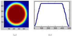
도 9는 도 7의 히팅 모듈의 온도 분포에 대한 사진(a)과 그래프(b)이다.
도 10은 도 7의 히팅 모듈에 공급되는 전력에 따른 온도 상승률에 대한 평가 그래프이다.1 is a schematic block diagram of a heat treatment apparatus using a VCSEL according to an embodiment of the present invention.
2 is a bottom view of the heating module of Fig. 1;
3 is an enlarged bottom view of the laser unit of Fig.
4 is a bottom view of a heating module according to another embodiment of the present invention.
FIG. 5 is a flow chart illustrating a process of activating a source / drain region of a flat substrate using a substrate thermal processing apparatus according to another embodiment of the present invention. Referring to FIG.
6 is a schematic block diagram of a substrate heat treatment apparatus using a VCSEL according to another embodiment of the present invention.
7 is a bottom view of the heating module of the substrate heat treatment apparatus of FIG.
Fig. 8 is an arrangement of the laser unit of Fig. 7; Fig.
FIG. 9 is a photograph (a) and a graph (b) of the temperature distribution of the heating module of FIG.
10 is an evaluation graph of a temperature rise rate according to electric power supplied to the heating module of FIG.
이하에서 실시예와 첨부된 도면을 통하여 본 발명의 VCSEL을 이용한 기판 열처리 장치 및 방법에 대하여 보다 구체적으로 설명한다.Hereinafter, an apparatus and a method for heat-treating a substrate using the VCSEL of the present invention will be described in more detail with reference to embodiments and accompanying drawings.
먼저, 본 발명의 일 실시예에 따른 VCSEL을 이용한 기판 열처리 장치의 구조에 대하여 설명한다.First, a structure of a substrate heat treatment apparatus using a VCSEL according to an embodiment of the present invention will be described.
도 1은 본 발명의 일 실시예에 따른 VCSEL을 이용한 열처리 장치의 개략적인 구성도이다. 도 2는 도 1의 히팅 모듈의 저면도이다. 도 3은 도 2의 레이저 유닛의 확대 저면도이다.1 is a schematic block diagram of a heat treatment apparatus using a VCSEL according to an embodiment of the present invention. 2 is a bottom view of the heating module of Fig. 1; 3 is an enlarged bottom view of the laser unit of Fig.
본 발명의 일 실시예에 따른 VCSEL을 이용한 기판 열처리 장치(100)는, 도 1 내지 도 3을 참조하면, 기판 지지판(110) 및 히팅 모듈(120)을 포함하여 형성된다. 상기 기판 열처리 장치(100)는 구체적으로 도시하지는 않았지만, 내부가 중공이며 열처리 분위기가 형성되는 열처리 챔버를 구비하며, 열처리 챔버 내부에 기판 지지판(110) 및 히팅 모듈(120)이 위치한다.1 to 3, the
상기 기판 열처리 장치(100)는 유리 기판 또는 플렉서블 기판에 형성되는 박막 트랜지스터를 구비하는 평판 기판(10)의 상부 또는 하부에서 소스 영역 또는 드레인 영역과 같은 액티베이션 영역에 VCSEL을 선택적으로 조사하여 액티베이션 공정과 같은 열처리 공정을 진행한다. 또한, 상기 기판 열처리 장치(100)는 유리 기판 또는 플렉서블 기판에 형성되는 비정질 실리콘 박막을 구비하는 평판 기판의 상부 또는 하부에서 비정질 실리콘 박막에 VCSEL을 조사하여 결정화 공정과 같은 열처리 공정을 진행한다.The
상기 기판 열처리 장치(100)는 면발광 레이저인 VCSEL을 평판 기판(10)의 소정 면적에 조사하여 열처리 공정을 진행한다. 상기 기판 열처리 장치(100)는 바람직하게는 평판 기판(10)에서 열처리가 필요한 열처리 영역의 전체 면적에 VCSEL을 동시에 조사하여 열처리를 진행한다. 예를 들면, 상기 기판 열처리 장치(100)는 평판 기판(10)에서 액티베이션 영역의 전체에 VCSEL을 조사하여 액티베이션 공정을 진행한다. 상기 기판 열처리 장치(100)는 액티베이션 영역을 전체적으로 균일하게 가열하므로 액티베이션 과정에서 평판 기판(10)의 열 수축 또는 변형을 최소화시킬 수 있다. 또한, 상기 기판 열처리 장치(100)는 평판 기판에서 비정질 실리콘 박막이 형성된 결정화 영역의 전체에 VCSEL을 조사하여 결정화 공정을 진행한다. 상기 기판 열처리 장치(100)는 결정화 영역을 전체적으로 균일하게 가열하므로 결정화 과정에서 평판 기판(10)의 열 수축 또는 변형을 최소화시킬 수 있다.The substrate
또한, 상기 기판 열처리 장치(100)는 공정 시간을 단축시킬 수 있다. 또한, 상기 기판 열처리 장치(100)는 가열 온도등을 고려하여 공정 시간을 수msec에서 수백 sec까지 조절할 수 있도록 한다.In addition, the substrate
상기 평판 기판(10)은 평판 디스플레이 장치인 액정 디스플레이 장치 또는 유기 발광 디스플레이 장치에 사용될 수 있다. 또한, 상기 평판 기판은 태양 전지와 같은 장치에도 사용될 수 있다.The
상기 기판 지지판(110)은 상면에 안착되는 평판 기판(10)보다 큰 면적을 갖는 판상으로 형성된다. 상기 평판 기판(10)은 유리 기판 또는 플렉서블 기판일 수 있다. 상기 기판 지지판(110)은 평판 디스플레이 장치용 평판 기판의 제조 사용되는 일반적인 기판 지지판으로 형성된다. 상기 기판 지지판(110)은 상면에 안착되는 평판 기판(10)을 고정하기 위한 척킹 수단(미도시)을 구비하여 형성될 수 있다.The
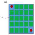
상기 히팅 모듈(120)은 히팅 프레임(121) 및 레이저 유닛(125)을 포함하여 형성된다. 상기 히팅 모듈(120)은 기판 지지판(110)의 상부 또는 하부에 위치하며, 기판 지지판(110)에 안착되는 평판 기판(10)에서 전체 열처리 영역에 레이저를 동시에 조사한다.The
상기 히팅 모듈(120)은 복수 개의 레이저 유닛(125)이 행 방향과 열 방향으로 배열되어 형성된다. 상기 히팅 모듈(120)은 평판 기판(10)의 면적보다 큰 면적에 레이저 유닛이 평면 형상으로 배열되도록 형성된다. 상기 히팅 모듈(120)은 평판 기판(10)의 액티베이션 온도와 평판 기판(10)의 면적에 따라 레이저 유닛(125)의 배열 간격과 개수가 달라질 수 있다.The
상기 히팅 모듈(120)은 레이저 유닛(125)과 평판 기판(10)의 상면 또는 하면과 소정 거리로 이격되도록 위치한다. 상기 이격 거리는 레이저 유닛(125)의 배열 간격과 배열 형태에 따라 평판 기판(10)의 열처리 영역 또는 액티베이션 영역만을 적정하게 가열할 수 있도록 조정된다.The
상기 히팅 프레임(121)은 전체적으로 판상을 이루도록 형성되며, 평판 기판(10)의 폭 및 길이보다 큰 폭과 길이를 갖는 사각 판상으로 형성된다. 상기 히팅 프레임(121)은 수용 홈(122)을 포함하여 형성될 수 있다. 한편, 상기 히팅 프레임(121)이 평판으로 형성되고 레이저 유닛(125)이 히팅 프레임의 하면에 직접 고정되는 경우에, 수용 홈(122)은 생략될 수 있다.The
상기 수용 홈(122)은 히팅 프레임에서 평판 기판과 대향하는 면에 하부 또는 상부로 개방되어 형성된다. 상기 수용 홈(122)은 격자 형상으로 배열되어 형성된다. 상기 수용 홈(122)은 레이저 유닛(125)이 수용되는 공간을 제공한다. 상기 수용 홈(122)은 레이저 유닛(125)이 수용되는데 필요한 부피를 갖도록 형성된다. 상기 수용 홈(122)은 레이저 유닛(125)이 분리 가능하게 결합되도록 형성될 수 있다.The receiving
상기 히팅 프레임(121)은 구체적으로 도시하지는 않았지만 내부에 냉각수가 흐르는 냉각 유로가 형성될 수 있다. 상기 히팅 프레임(121)은 수용 홈(122)에 수용되는 레이저 유닛(125)과 접촉하면서 외부로부터 공급되는 냉각수를 이용하여 레이저 유닛(125)을 냉각할 수 있다. 이 경우에 상기 히팅 프레임(121)은 전체 레이저 유닛(125)을 냉각하게 된다. 상기 레이저 유닛(125)은 작동할 때 발생되는 열에 수명이 저하될 수 있다.The
한편, 상기 히팅 프레임(121)은 각각의 레이저 유닛(125)에 냉각수를 공급하도록 냉각 유로가 형성될 수 있다. 즉, 상기 히팅 프레임(121)은 각각의 수용 홈(122)에 수용되는 레이저 유닛(125)에 직접 냉각수가 공급되도록 냉각 유로가 형성될 수 있다. 또한, 상기 레이저 유닛(125)은 후면에 냉각수가 흐르는 냉각 유로가 개별적으로 형성될 수 있다. 이 경우에 상기 레이저 유닛은 히팅 프레임(121)에서 공급되는 냉각수에 의하여 개별적으로 냉각된다.Meanwhile, the
상기 레이저 유닛(125)은 적어도 1개의 VCSEL 소자(126)를 포함하여 형성된다. 상기 레이저 유닛(125)은 바람직하게는 복수 개의 VCSEL 소자(126)가 평면상으로 사각 형상을 이루도록 배열되어 형성된다. 예를 들면, 상기 레이저 유닛(125)은, 도 3을 참조하면, 복수 개의 VCSEL 소자(126)가 행 방향과 열 방향으로 배열되어 형성된다. 상기 레이저 유닛(125)은 구체적으로 도시하는 않았지만, VCSEL 소자(126)를 고정하기 위한 발광 프레임(미도시)과 VCSEL 소자(126)에 전력을 공급하기 위한 전력선 및 전력 입출력 단자(미도시)를 구비하여 형성될 수 있다. 상기 레이저 유닛(125)은 전체에 동일한 전력이 인가되도록 형성될 수 있다. 또한, 상기 레이저 유닛(125)은 각각에 서로 다른 전력이 인가되도록 형성될 수 있다. 이러한 경우에, 상기 레이저 유닛(125)은 VCSEL 소자(126)에 인가되는 전력을 제어하는 제어 소자를 포함할 수 있다.The
상기 VCSEL 소자(126)는 면발광 레이저를 발진하는 소자로 형성된다. 상기 VCSEL 소자(126)는 사각 형상으로 이루어지며, 바람직하게는 정사각형 또는 폭과 길이의 비가 1:2를 초과하지 않는 직사각형 형상으로 형성될 수 있다. 상기 VCSEL 소자(126)는 육면체 형상의 칩으로 제조되며, 일면에서 고출력의 레이저가 발진된다. 상기 VCSEL 소자(126)는 고출력의 레이저를 발진하므로, 기존의 할로겐 램프에 대비하여 평판 기판(10)의 온도 상승률을 증가시킬 수 있으며, 수명도 상대적으로 길다.The
다음은 본 발명의 다른 실시예에 따른 히팅 모듈에 대하여 설명한다.Next, a heating module according to another embodiment of the present invention will be described.
본 발명의 다른 실시예에 따른 히팅 모듈(220)은, 도 4를 참조하면, 히팅 프레임(221) 및 레이저 유닛(225)을 포함하여 형성된다.Referring to FIG. 4, the
상기 히팅 모듈(220)은 복수 개의 레이저 유닛(225)이 길이 방향으로 배열되어 형성된다. 상기 히팅 모듈(220)은 평판 기판(10)의 폭보다 큰 길이에 걸쳐서 레이저 유닛(225)이 배열되도록 형성된다. 상기 히팅 모듈(220)은 평판 기판(10)의 열처리 온도와 평판 기판(10)의 폭에 따라 레이저 유닛(225)의 배열 간격과 개수가 달라질 수 있다. 한편, 여기서, 상기 평판 기판(10)의 폭은 길이가 될 수 있으며, 선택적인 개념이다.The
상기 히팅 모듈(220)은 평판 기판의 폭의 전체와 평판 기판의 소정 길이의 영역에 대하여 동시에 VCSEL을 조사한다. 또한, 상기 히팅 모듈(220)은 평판 기판(10)을 길이 방향으로 스캔하면서 레이저를 조사한다. 따라서, 상기 히팅 모듈은 평판 기판의 폭 방향의 전체에 대하여 동시에 VCSEL을 조사하고 길이 방향으로 스캔하면서 VCSEL을 조사하여 열처리를 진행하므로 평판 기판의 폭 방향으로의 수축 또는 변형등을 감소시킬 수 있다.The
상기 히팅 모듈(220)은 히팅 프레임(221)과 레이저 유닛(225)을 이동시키기 위한 이동 유닛(미도시)을 더 포함하여 형성될 수 있다. 상기 이동 유닛은 반도체 또는 평판 디스플레이 장치의 제조 장치에서 사용되는 일반적인 이동 장치로 형성될 수 있다. 또한, 상기 히팅 모듈(220)은 레이저 유닛(225)의 작동을 제어하는 별도의 제어 유닛(미도시)을 구비하여 형성될 수 있다. 한편, 본 발명의 다른 실시예에 따른 히팅 모듈(220)은 도 1 내지 도 3의 기판 열처리 장치(100)에 장착되어 사용된다.The
상기 히팅 프레임(221)은 길이 방향으로 연장되어 전체적으로 바 형상을 이루도록 형성되며, 길이가 평판 기판(10)의 폭 또는 길이보다 크게 형성된다. 상기 히팅 프레임(221)은 복수 개의 수용 홈(222)이 형성된다.The heating frame 221 extends in the longitudinal direction and is formed to have a bar shape as a whole, and is formed to have a length greater than the width or length of the
상기 수용 홈(222)은 히팅 프레임(221)에서 평판 기판(10)과 대향하는 면인 하면 또는 상면에 홈 형상으로 형성된다. 상기 수용 홈(222)은 레이저 유닛(225)이 수용되는 공간을 제공한다. 상기 수용 홈(222)은 히팅 프레임(221)에서 길이 방향으로 배열된다. 상기 수용 홈(222)은 서로 접하거나 이격되어 형성된다.The receiving
상기 레이저 유닛(225)은 적어도 1개의 VCSEL 소자(126)를 포함하여 형성된다. 상기 레이저 유닛(225)은, 도 4를 참조하면, 히팅 프레임(221)에 길이 방향으로 한 줄로 배열되어 형성된다. 상기 레이저 유닛(225)은 수용 홈(222)에 삽입되어 고정된다. 상기 레이저 유닛(225)은 수용 홈(222)에 분리 가능하게 결합될 수 있다.The
상기 히팅 모듈(220)은 평판 기판(10)의 상부 또는 하부에서 평판 기판(10)을 스캔하면서 액티베이션 영역과 같은 열처리 영역에 레이저를 조사한다. 따라서, 상기 히팅 모듈(220)이 이동하여 액티베이션 영역에 위치하면, 레이저 유닛(225)의 VCSEL 소자(126)가 작동하여 해당 액티베이션 영역에 레이저를 조사한다. 또한, 상기 히팅 모듈(220)이 액티베이션 영역을 지나면, 해당 VCSEL 소자(126)는 작동을 중지한다.The
다음은 본 발명의 일 실시예에 따른 기판 열처리 장치를 이용한 액티베이션 방법에 대하여 설명한다.Next, an activation method using a substrate heat treatment apparatus according to an embodiment of the present invention will be described.
도 5는 본 발명의 일 실시예에 따른 기판 열처리 장치를 이용하여 평판 기판의 소스/드레인 영역의 액티베이션 공정을 진행하는 공정도이다.FIG. 5 is a process diagram illustrating a process of activating a source / drain region of a flat substrate using a substrate thermal processing apparatus according to an embodiment of the present invention. Referring to FIG.
상기 기판 열처리 장치(100)는, 도 5를 참조하면, 플렉서블 기판(10)의 상면에 형성되는 저온 단결정 실리콘 박막 트랜지스터의 소스 영역과 드레인 영역에 레이저를 조사하여 액티베이션 공정을 진행한다. 상기 저온 단결정 실리콘 박막 트랜지스터는 소스 영역과 드레인 영역에 이온이 주입되고 액티베이션되어 형성된다.5, the substrate
상기 기판 열처리 장치(100)의 히팅 모듈(120)이 투명한 플렉서블 기판(10)의 하부에 위치하여 플렉서블 기판(10)의 액티베이션 영역으로 레이저를 동시에 조사한다. 상기 VCSEL 소자(126)에서 조사되는 레이저는 대략 980nm의 파장을 가지며, 약 98%이상이 플렉서블 기판(10)을 투과하여 소스 영역 및 드레인 영역에 조사된다. 따라서, 상기 기판 열처리 장치(100)는 소스 영역과 드레인 영역에 대응되는 위치에 배열되는 레이저 유닛(125)을 선택적으로 작동시켜 레이저를 조사할 수 있다. 상기 기판 열처리 장치(100)는 소스 영역과 드레인 영역만을 선택적으로 조사하여 가열하므로, 플렉서블 기판(10)의 열 수축 또는 변형을 최소화시킬 수 있다.The
다음은 본 발명의 또 다른 실시예에 따른 기판 열처리 장치에 대하여 설명한다.Next, a substrate heat treatment apparatus according to another embodiment of the present invention will be described.
도 6은 본 발명의 또 다른 실시예에 따른 VCSEL을 이용한 기판 열처리 장치의 개략적인 구성도이다. 도 7은 도 6의 기판 열처리 장치의 히팅 모듈에 대한 저면도이다. 도 8은 도 6의 히팅 모듈에서 레이저 유닛의 배열 구조를 나타낸다.6 is a schematic block diagram of a substrate heat treatment apparatus using a VCSEL according to another embodiment of the present invention. 7 is a bottom view of the heating module of the substrate heat treatment apparatus of FIG. 8 shows the arrangement of laser units in the heating module of Fig.
본 발명의 또 다른 실시예에 따른 VCSEL을 이용한 기판 열처리 장치(300)는, 도 6 내지 도 8을 참조하면, 기판 지지판(310)과 히팅 모듈(320) 및 회전 모듈(330)을 포함하여 형성된다. 상기 기판 열처리 장치(300)는 구체적으로 도시하지는 않았지만, 내부가 중공이며 열처리 분위기가 형성되는 열처리 챔버를 구비하며, 열처리 챔버 내부에 기판 지지판(310)과 히팅 모듈(320)이 위치한다. 또한, 상기 기판 열처리 장치(300)는 히팅 모듈(320)에서 발진되는 VCSEL을 기판 지지판(310)에 안착되는 반도체 웨이퍼(20)의 소정 면적에 동시에 조사하여 반도체 웨이퍼(20)를 열처리한다. 상기 열처리는 반도체 웨이퍼(20)의 상면에 형성되는 비정질 실리콘 박막의 결정화 공정 또는 반도체 웨이퍼(20)의 어닐링 공정일 수 있다. 상기 기판 열처리 장치(300)는 바람직하게는 반도체 웨이퍼(20)에서 열처리가 필요한 열처리 영역의 전체 면적에 동시에 VCSEL을 조사하여 가열한다. 상기 기판 열처리 장치는 반도체 웨이퍼(2)의 전체 면적을 동시에 가열하므로 온도 균일도가 증가하고 공정 시간을 단축시킬 수 있다. 또한, 상기 기판 열처리 장치는 가열 온도등을 고려하여 공정 시간을 수msec에서 수백 sec까지 조절할 수 있도록 한다.한편, 상기 기판 열처리 장치(300)는 히팅 모듈(320)이 기판 지지판(310)의 하부에 위치하여 반도체 웨이퍼(20)의 하면에 레이저를 조사하도록 형성될 수 있다.6 to 8, a
상기 기판 지지판(310)은 상면에 안착되는 반도체 웨이퍼(20)의 직경보다 큰 폭과 길이를 갖는 판상으로 형성된다. 상기 기판 지지판(310)은 반도체 제조 공정에서 사용되는 일반적인 기판 지지판(310)으로 형성될 수 있다. 상기 웨이퍼 지지판(100)은 상면에 안착되는 반도체 웨이퍼(20)를 고정하기 위한 척킹 수단(미도시)을 구비하여 형성될 수 있다.The
상기 히팅 모듈(320)은 히팅 프레임(321) 및 레이저 유닛(325)을 포함하여 형성된다. 상기 히팅 모듈(320)은 기판 지지판(310)의 상부에 위치하며, 기판 지지판(310)에 안착되는 반도체 웨이퍼(20)의 상면의 전체 면적에 동시에 레이저를 조사한다. 한편, 상기 히팅 모듈(320)은 기판 지지판(310)의 하부에 위치하며, 기판 지지판(310)의 상면에 안착되는 반도체 웨이퍼(20)의 하면에 레이저를 조사하도록 형성될 수 있다.The
상기 히팅 모듈(320)은 레이저 유닛(325)과 반도체 웨이퍼(20)의 가열면(상면 또는 하면) 사이의 이격 거리가 50 ~ 400mm가 되도록 반도체 웨이퍼(20)의 상부 또는 하부에 위치한다. 상기 이격 거리는 바람직하게는 100 ~ 300mm일 수 있다. 상기 이격 거리는 레이저 유닛(325)의 배열 간격과 배열 형태에 따라 반도체 웨이퍼(20)가 균일하게 가열될 수 있도록 조정될 수 있다. 예를 들면, 상기 레이저 유닛(325)의 배열 간격이 좁으면, 이격 거리가 작더라도 온도 균일도에 주는 영향이 작으므로 이격 거리를 작게 할 수 있다. 상기 이격 거리가 작은 경우에 공급되는 전력을 줄이거나 온도 상승률을 증가시킬 수 있다. 그러나, 상기 레이저 유닛(325)의 배열 간격이 넓고 이격 거리가 작으면, 온도 균일도가 감소하게 되므로, 배열 간격이 넓은 경우에 이격 거리를 상대적으로 크게 해야 한다. 상기 이격 거리가 긴 경우에 상대적으로 공급되는 전력을 증가시켜야 한다. 보다 구체적인 예를 들면, 상기 레이저 유닛(325)의 배열 간격이 24mm인 경우에, 레이저 유닛(325)과 반도체 웨이퍼(20)의 이격 거리가 150mm이면 온도 편차가 0.27℃(0.037%)이며, 200mm이면 0.15℃(0.018%)로 평가되었다. 이때, 상기 히팅 모듈(320)의 폭과 길이는 355mm이고, 반도체 웨이퍼(20)의 상면 온도는 800℃이고, 에너지 밀도는 각각 29.1W/㎠와 28.5W/㎠이었으며, 반도체 웨이퍼(20)의 회전 속도는 150rpm이었다. 한편, 다른 조건은 동일한 상태에서 반도체 웨이퍼(20)를 회전시키지 않는 경우에 온도 편차가 각각 2.96℃(0.37%)와 1.02℃(0.13%)로 증가되었다.The
상기 히팅 모듈(320)은 복수 개의 레이저 유닛(325)이 행 방향과 열 방향으로 배열되어 형성된다. 상기 히팅 모듈(320)은 반도체 웨이퍼(20)의 면적에 대응되는 면적의 영역에 레이저 유닛(325)이 위치하도록 형성될 수 있다. 예를 들면, 상기 히팅 모듈(320)은 반도체 웨이퍼(20)의 직경에 대응되는 직경을 갖는 원형의 영역에 레이저 유닛(325)이 배치될 수 있다.The
상기 히팅 프레임(321)은 전체적으로 판상을 이루도록 형성되며, 열처리되는 반도체 웨이퍼(20)의 직경보다 큰 폭과 길이를 갖는 사각 판상 또는 반도체 웨이퍼(20)의 직경보다 큰 직경을 갖는 원 형상으로 형성될 수 있다. 상기 히팅 프레임(321)은 수용 홈(322)을 포함하여 형성될 수 있다.The
상기 수용 홈(322)은 히팅 프레임(321)에서 반도체 웨이퍼(20)와 대향하는 면에 개방되어 형성되며, 행 방향과 열 방향으로 배열되어 격자 형상을 이루도록 형성된다. 상기 수용 홈(322)은 레이저 유닛(325)이 수용되는 공간을 제공한다. 상기 수용 홈(322)은 히팅 프레임(321)의 하면의 전체 영역에 형성될 수 있으며, 반도체 웨이퍼(20)의 면적에 대응되는 영역에만 형성될 수 있다.The receiving
상기 레이저 유닛(325)은 적어도 1개의 VCSEL 소자(126)를 포함하여 형성된다. 상기 레이저 유닛(325)은 바람직하게는, 도 3에 도시된 바와 같이 복수 개의 VCSEL 소자(126)가 평면상으로 사각 형상을 이루도록 배열되어 형성된다.The
상기 레이저 유닛(325)은 히팅 프레임(321)에 행 방향과 열 방향으로 배열되어 형성된다. 이때, 상기 레이저 유닛(325)은, 도 7에서 보는 바와 같이, 행 방향과 열 방향으로 한 개씩 이격되어 배열될 수 있다. 또한, 상기 레이저 유닛(325)은 행 방향과 열 방향으로 격자 형상으로 배열되고, 도 7에서 보는 바와 같이, 한 개 건너 한 개씩 교대로 작동될 수 있다.The
상기 레이저 유닛(325)은 반도체 웨이퍼(20)의 최고 가열 온도 또는 온도 상승 속도에 따라 다른 개수로 배열될 수 있다. 예를 들면, 상기 레이저 유닛(325)은 도 8의 (a)에서 보는 바와 같이 격자 형상을 이루는 수용 홈(322)의 전체에 각각 위치하도록 배열될 수 있다. 또한, 상기 레이저 유닛(325)은, 도 8의 (b)에서 보는 바와 같이 사각 형상으로 이루도록 인접하는 4개의 수용 홈(322)에서 대각선 방향으로 2개만 위치하도록 배열될 수 있다. 상기 레이저 유닛(325)은 도 8의 (b)와 같이 배열되는 경우에 행 방향과 열 방향으로 교대로 배열되는 구조가 된다. 또한, 상기 레이저 유닛(325)은 도 8의 (c)에서 보는 바와 같이 사각 형상을 이루도록 인접하는 4개의 수용 홈(322)에서 어느 하나에만 위치하도록 배열될 수 있다. 이러한 경우에 에너지 밀도는 각각 100W/㎠, 50W/㎠, 25W/㎠가 된다. 상기 레이저 유닛(325)이 도 8의 (a)와 같이 배열되는 경우에 반도체 웨이퍼(20)의 가열 온도 또는 온도 상승률이 상대적으로 높게 되며, 도 8의 (c)와 같이 배열되는 경우에 반도체 웨이퍼(20)의 가열 온도 또는 온도 상승률이 상대적으로 낮게 된다. 한편, 상기 레이저 유닛(325)은 반도체 웨이퍼(20)가 회전하는 상태에서 레이저를 조사하는 경우에 도 8의 (b) 또는 (c)와 같이 배열되더라도 반도체 웨이퍼(20)를 불균일하게 가열하지 않는다.The
상기 회전 모듈(330)은 기판 지지판(310)의 하부에 결합되며, 기판 지지판(310)을 회전시킨다. 상기 기판 지지판(310)이 회전되는 경우에 기판 지지판(310)의 상면에 안착되어 있는 반도체 웨이퍼(20)는 보다 균일하게 가열된다.The
상기 회전 모듈(330)은 기존의 반도체 웨이퍼 열처리 장치에서 사용되는 회전 모듈로 형성될 수 있다. 예를 들면, 상기 회전 모듈(330)은, 구체적으로 도시하지는 않았지만, 기판 지지판(310)의 하부에 결합되는 회전축과 회전축을 회전시키는 모터 및 회전축과 모터를 연결시키는 타이밍 벨트 또는 체인을 포함하여 형성될 수 있다. 또한, 상기 회전축에 직접 모터가 연결되어 회전축과 기판 지지판(310)을 회전시키도록 형성될 수 있다. 또한, 기판 지지판(310)이 중공으로 형성되어 히팅 모듈(320)이 하부에 형성될 수 있다.The
다음은 본 발명의 일 실시예에 따른 히팅 모듈의 평가 결과에 대하여 설명한다.Next, evaluation results of the heating module according to one embodiment of the present invention will be described.
도 9는 도 7의 히팅 모듈에 대하여 시뮬레이션 과정을 통하여 평가한 결과이다. 도 7의 히팅 모듈에 대한 평가에서는 히팅 모듈(320)과 반도체 웨이퍼(20) 사이의 거리를 300mm로 하였다. 또한, 상기 히팅 모듈(320)은 반도체 웨이퍼(20)의 면적에 대응되는 영역에 위치하는 레이저 유닛(325)에 반도체 웨이퍼(20)의 가열 온도에 필요한 전력을 공급하고, 반도체 웨이퍼(20)의 외측 영역에 위치하는 레이저 유닛(325)에 대하여는 외측으로 갈수록 공급되는 전력을 감소시켰다. 도 9의 (a)에서 보는 바와 같이 시뮬레이션 결과를 참조하면, 히팅 모듈(320)은 반도체 웨이퍼(20)에 대응되는 영역의 온도가 가장 높으며, 외측으로 갈수록 온도가 낮아지도록 작동한다. 도 9의 (b)를 보면, 반도체 웨이퍼(20)의 직경에 대응되는 길이에서 온도 분포가 균일하며, 반도체 웨이퍼(20)의 외측으로 갈수록 온도가 급격하게 감소되는 것을 볼 수 있다. 평가 결과에 따르면, 온도가 균일한 영역에서의 온도 편차는 0.746%로 평가되었다.FIG. 9 is a result of evaluation of the heating module of FIG. 7 through a simulation process. 7, the distance between the
또한, 상기 반도체 웨이퍼(20)의 표면 온도는 800℃이고, 온도 상승률은 75℃/sec이고, 인가되는 전력이 26.9kW이고, 최대 에너지 밀도가 29.1W/㎠이며, 반도체 웨이퍼(20)와의 거리가 150mm인 경우에 온도 균일도가 0.3℃이하로 평가되었다. 이때, 상기 반도체 웨이퍼(20)는 150rpm으로 회전시켰다.The surface temperature of the
다음은 히팅 모듈에 인가되는 전력에 따른 온도 상승률에 대한 평가 결과이다.The following is the evaluation result of the temperature rise rate according to the power applied to the heating module.
도 10을 참조하면, 상기 히팅 모듈(320)의 에너지 밀도가 높을수록 온도 상승률과 반도체 웨이퍼(20)의 표면 최고 온도가 증가되는 것을 알 수 있다. 또한, 상기 히팅 모듈(320)의 에너지 밀도가 높을수록 반도체 웨이퍼(20)의 표면 최고 온도에 도달하는 시간이 감소되는 것을 알 수 있다.Referring to FIG. 10, it can be seen that as the energy density of the
본 명세서에 개시된 실시예는 여러 가지 실시 가능한 예중에서 당업자의 이해를 돕기 위하여 가장 바람직한 실시예를 선정하여 제시한 것일 뿐, 이 발명의 기술적 사상이 반드시 이 실시예에만 의해서 한정되거나 제한되는 것은 아니고, 본 발명의 기술적 사상을 벗어나지 않는 범위 내에서 다양한 변화와 부가 및 변경이 가능함 물론, 균등한 다른 실시예의 구현이 가능하다.It is to be understood that both the foregoing general description and the following detailed description of the present invention are exemplary and explanatory and are intended to provide further explanation of the invention as claimed. It will be understood by those skilled in the art that various changes in form and details may be made therein without departing from the spirit and scope of the invention as defined in the appended claims.
10: 평판 기판20: 반도체 웨이퍼
100, 300: 기판 열처리 장치
110, 310: 기판 지지판120, 220, 320: 히팅 모듈
121, 221,321: 히팅 프레임125, 225, 325: 레이저 유닛
330: 회전 모듈10: flat plate substrate 20: semiconductor wafer
100, 300: Substrate heat treatment apparatus
110, 310:
121, 221, 321:
330: Rotation module
Claims (12)
Translated fromKorean상기 평판 기판의 소정 면적에 VCSEL을 동시에 조사하여 열처리 공정을 진행하는 히팅 모듈을 포함하는 것을 특징으로 하는 기판 열처리 장치.A substrate support plate on which the flat plate substrate is mounted, and
And a heating module for simultaneously applying a VCSEL to a predetermined area of the flat substrate to conduct a heat treatment process.
상기 평판 기판은 소스 영역과 드레인 영역을 포함하는 박막 트랜지스터가 형성되는 유리 기판 또는 플렉서블 기판 또는 비정질 실리콘 박막이 형성되는 유리 기판 또는 플렉서블 기판인 것을 특징으로 하는 기판 열처리 장치.The method according to claim 1,
Wherein the flat substrate is a glass substrate or a flexible substrate on which a thin film transistor including a source region and a drain region is formed, or a glass substrate or a flexible substrate on which an amorphous silicon thin film is formed.
상기 히팅 모듈은
상기 평판 기판의 폭 및 길이보다 큰 폭과 길이를 갖는 히팅 프레임 및
상기 평판 기판의 폭 및 길이보다 큰 폭과 길이를 갖는 영역에 행 방향과 열 방향으로 배열되어 VCSEL을 발진하는 레이저 유닛을 포함하며,
상기 히팅 모듈은 상기 평판 기판에서 열처리를 필요로 하는 영역의 전체 면적에 동시에 VCSEL을 조사하도록 형성되는 것을 특징으로 하는 기판 열처리 장치.3. The method of claim 2,
The heating module
A heating frame having a width and a length greater than the width and length of the flat substrate; and
And a laser unit arranged in a row direction and in a column direction in an area having a width and a length greater than the width and length of the flat substrate to oscillate the VCSEL,
Wherein the heating module is formed to simultaneously irradiate a VCSEL to the entire area of a region requiring heat treatment in the flat plate substrate.
상기 히팅 모듈은
길이 방향으로 연장되며, 상기 평판 기판의 폭보다 큰 길이를 갖는 히팅 프레임 및
상기 히팅 프레임에 상기 평판 기판의 폭보다 큰 길이로 배열되어 VCSEL을 발진하는 레이저 유닛을 포함하며,
상기 히팅 모듈은 상기 평판 기판의 전체 폭 및 소정 길이의 영역에 동시에 VCSEL을 조사하며 상기 평판 기판의 길이 방향으로 스캔하면서 VCSEL을 조사하도록 형성되는 것을 특징으로 하는 기판 열처리 장치.3. The method of claim 2,
The heating module
A heating frame extending in the longitudinal direction and having a length greater than the width of the flat substrate, and
And a laser unit arranged on the heating frame at a length greater than the width of the flat substrate to oscillate the VCSEL,
Wherein the heating module is formed to simultaneously irradiate a VCSEL to the entire width and a predetermined length of the flat substrate and irradiate the VCSEL while scanning the flat substrate in the longitudinal direction of the flat substrate.
상기 히팅 프레임은 상기 평판 기판과 대향하는 면에 형성되는 수용 홈을 구비하며,
상기 레이저 유닛은 상기 수용 홈에 분리 가능하게 결합되는 것을 특징으로 하는 기판 열처리 장치.The method according to claim 3 or 4,
Wherein the heating frame has a receiving groove formed on a surface facing the flat substrate,
And the laser unit is detachably coupled to the receiving groove.
상기 기판은 반도체 웨이퍼로 형성되며,
상기 기판 지지판의 하부에 결합되어 상기 기판 지지판을 회전시키는 회전 모듈을 더 포함하며,
상기 히팅 모듈은 상기 반도체 웨이퍼의 직경보다 큰 폭과 길이를 갖는 히팅 프레임 및 상기 히팅 프레임에 행 방향과 열 방향으로 배열되어 VCSEL을 발진하는 레이저 유닛을 포함하며,
상기 히팅 모듈은 상기 반도체 웨이퍼의 전체 면적에 동시에 VCSEL을 조사하도록 형성되는 것을 특징으로 하는 기판 열처리 장치.The method according to claim 1,
Wherein the substrate is formed of a semiconductor wafer,
And a rotation module coupled to a lower portion of the substrate support plate to rotate the substrate support plate,
Wherein the heating module includes a heating frame having a width and a length greater than the diameter of the semiconductor wafer and a laser unit arranged in the row direction and the column direction in the heating frame to oscillate the VCSEL,
Wherein the heating module is formed to simultaneously irradiate a VCSEL to the entire area of the semiconductor wafer.
상기 히팅 프레임은 상기 반도체 웨이퍼와 대향하는 면에 행 방향과 열 방향으로 배열되어 격자 형상을 이루도록 형성되는 수용 홈을 구비하며,
상기 레이저 유닛은 상기 수용 홈에 분리 가능하게 결합되는 것을 특징으로 하는 기판 열처리 장치.The method according to claim 6,
Wherein the heating frame has a receiving groove formed in a row direction and a column direction on a surface facing the semiconductor wafer so as to form a lattice shape,
And the laser unit is detachably coupled to the receiving groove.
상기 레이저 유닛은 상기 수용 홈에 모두 결합되거나, 사각 형상을 이루도록 인접하는 4개의 상기 수용 홈에서 대각선 방향으로 2개에만 결합되거나, 사각 형상을 이루도록 인접하는 4개의 상기 수용 홈에서 어느 하나에만 결합되는 것을 특징으로 하는 기판 열처리 장치.8. The method of claim 7,
The laser unit may be coupled to only two of the four receiving grooves so as to form a rectangular shape, or may be coupled to only one of the four receiving grooves so as to have a rectangular shape And the substrate is heated.
상기 열처리 공정은 유리 기판 또는 플렉서블 기판에 형성되는 박막 트랜지스터의 소스 영역 및 드레인 영역에 대한 액티베이션 공정, 상기 유리 기판 또는 플렉서블 기판에 형성되는 비정질 실리콘 박막의 결정화 공정 또는 상기 반도체 웨이퍼를 가열하는 가열 공정인 것을 특징으로 하는 기판 열처리 방법.10. The method of claim 9,
The heat treatment process may include an activation process for a source region and a drain region of a thin film transistor formed on a glass substrate or a flexible substrate, a crystallization process of the amorphous silicon thin film formed on the glass substrate or the flexible substrate, ≪ / RTI >
상기 열처리 공정은 상기 평판 기판에서 열처리가 필요한 영역 또는 상기 반도체 웨이퍼에서 열처리가 필요한 영역의 전체에 VCSEL을 동시에 조사하여 진행되는 것을 특징으로 하는 기판 열처리 방법.10. The method of claim 9,
Wherein the heat treatment process is performed by simultaneously irradiating a VCSEL to a region requiring heat treatment in the flat substrate or an entire region requiring heat treatment in the semiconductor wafer.
상기 열처리 공정은 상기 평판 기판의 전체 폭과 소정 길이의 영역에 동시에 VCSEL을 조사하며, 상기 평판 기판의 길이 방향으로 스캔하면서 VCSEL을 조사하여 진행되는 것을 특징으로 하는 기판 열처리 방법.10. The method of claim 9,
Wherein the heat treatment process is performed by simultaneously irradiating a VCSEL to the entire width and a predetermined length of the flat substrate and irradiating the VCSEL while scanning the flat substrate in the longitudinal direction of the flat substrate.
Priority Applications (1)
| Application Number | Priority Date | Filing Date | Title |
|---|---|---|---|
| KR1020160181167AKR102147379B1 (en) | 2016-12-28 | 2016-12-28 | Heat-Treatment Apparatus and Method of Substrate using VCSEL |
Applications Claiming Priority (1)
| Application Number | Priority Date | Filing Date | Title |
|---|---|---|---|
| KR1020160181167AKR102147379B1 (en) | 2016-12-28 | 2016-12-28 | Heat-Treatment Apparatus and Method of Substrate using VCSEL |
Publications (2)
| Publication Number | Publication Date |
|---|---|
| KR20180077384Atrue KR20180077384A (en) | 2018-07-09 |
| KR102147379B1 KR102147379B1 (en) | 2020-08-25 |
Family
ID=62919546
Family Applications (1)
| Application Number | Title | Priority Date | Filing Date |
|---|---|---|---|
| KR1020160181167AActiveKR102147379B1 (en) | 2016-12-28 | 2016-12-28 | Heat-Treatment Apparatus and Method of Substrate using VCSEL |
Country Status (1)
| Country | Link |
|---|---|
| KR (1) | KR102147379B1 (en) |
Cited By (6)
| Publication number | Priority date | Publication date | Assignee | Title |
|---|---|---|---|---|
| KR20200082699A (en)* | 2018-12-31 | 2020-07-08 | 주식회사 비아트론 | A laser chip module and a laser chip module array including a VCSEL |
| CN113555772A (en)* | 2020-04-23 | 2021-10-26 | 普罗科技有限公司 | Flip chip bonding apparatus using vertical cavity surface emitting laser element |
| WO2021246579A1 (en)* | 2020-06-02 | 2021-12-09 | ㈜비아트론 | Substrate heat-treatment apparatus using vcsel |
| WO2022146075A1 (en)* | 2020-12-31 | 2022-07-07 | 주식회사 비아트론 | Flat substrate heating device using laser light-emitting element |
| CN115077211A (en)* | 2021-03-11 | 2022-09-20 | 韩国光洋热电系统有限公司 | Exhaust duct integrated heater unit for heat treatment furnace |
| CN115740746A (en)* | 2022-11-25 | 2023-03-07 | 深圳市鑫宸锐智能科技有限公司 | VCSEL laser welding equipment and welding method |
Families Citing this family (2)
| Publication number | Priority date | Publication date | Assignee | Title |
|---|---|---|---|---|
| KR20250124900A (en) | 2024-02-13 | 2025-08-21 | 에이피시스템 주식회사 | Light emitting module and heater block containing the same |
| KR102756061B1 (en) | 2024-06-26 | 2025-01-21 | 주식회사 씨티랩 | Light-emitting module applied to heater block |
Citations (3)
| Publication number | Priority date | Publication date | Assignee | Title |
|---|---|---|---|---|
| JP2006059931A (en)* | 2004-08-18 | 2006-03-02 | Canon Anelva Corp | Rapid heat treatment equipment |
| KR20090017084A (en)* | 2007-08-14 | 2009-02-18 | 주식회사 코윈디에스티 | Laser heat treatment apparatus and its heat treatment method |
| WO2015107009A1 (en)* | 2014-01-17 | 2015-07-23 | Koninklijke Philips N.V. | Heating system comprising semiconductor light sources |
- 2016
- 2016-12-28KRKR1020160181167Apatent/KR102147379B1/enactiveActive
Patent Citations (3)
| Publication number | Priority date | Publication date | Assignee | Title |
|---|---|---|---|---|
| JP2006059931A (en)* | 2004-08-18 | 2006-03-02 | Canon Anelva Corp | Rapid heat treatment equipment |
| KR20090017084A (en)* | 2007-08-14 | 2009-02-18 | 주식회사 코윈디에스티 | Laser heat treatment apparatus and its heat treatment method |
| WO2015107009A1 (en)* | 2014-01-17 | 2015-07-23 | Koninklijke Philips N.V. | Heating system comprising semiconductor light sources |
Cited By (11)
| Publication number | Priority date | Publication date | Assignee | Title |
|---|---|---|---|---|
| KR20200082699A (en)* | 2018-12-31 | 2020-07-08 | 주식회사 비아트론 | A laser chip module and a laser chip module array including a VCSEL |
| CN113555772A (en)* | 2020-04-23 | 2021-10-26 | 普罗科技有限公司 | Flip chip bonding apparatus using vertical cavity surface emitting laser element |
| CN113555772B (en)* | 2020-04-23 | 2024-11-15 | 普罗科技有限公司 | Flip chip bonding device using vertical cavity surface emitting laser element |
| WO2021246579A1 (en)* | 2020-06-02 | 2021-12-09 | ㈜비아트론 | Substrate heat-treatment apparatus using vcsel |
| KR20210149382A (en)* | 2020-06-02 | 2021-12-09 | 주식회사 비아트론 | Apparatus For Heat-Treatment of Substrate using VCSEL |
| KR20220127796A (en)* | 2020-06-02 | 2022-09-20 | 주식회사 비아트론 | Apparatus For Heat-Treatment of Substrate using VCSEL |
| CN115699283A (en)* | 2020-06-02 | 2023-02-03 | 微传科技有限公司 | Substrate heat treatment apparatus using vertical cavity surface emitting laser |
| CN115699283B (en)* | 2020-06-02 | 2025-07-29 | 微传科技有限公司 | Substrate heat treatment apparatus using vertical cavity surface emitting laser |
| WO2022146075A1 (en)* | 2020-12-31 | 2022-07-07 | 주식회사 비아트론 | Flat substrate heating device using laser light-emitting element |
| CN115077211A (en)* | 2021-03-11 | 2022-09-20 | 韩国光洋热电系统有限公司 | Exhaust duct integrated heater unit for heat treatment furnace |
| CN115740746A (en)* | 2022-11-25 | 2023-03-07 | 深圳市鑫宸锐智能科技有限公司 | VCSEL laser welding equipment and welding method |
Also Published As
| Publication number | Publication date |
|---|---|
| KR102147379B1 (en) | 2020-08-25 |
Similar Documents
| Publication | Publication Date | Title |
|---|---|---|
| KR20180077384A (en) | Heat-Treatment Apparatus and Method of Substrate using VCSEL | |
| CN106340451B (en) | Heat treatment method and heat treatment apparatus | |
| KR102444062B1 (en) | Substrate heat treatment apparatus using VCSEL | |
| US8050546B2 (en) | Heat treatment apparatus heating substrate by irradiation with light | |
| US9685303B2 (en) | Apparatus for heating and processing a substrate | |
| KR101868378B1 (en) | Managing thermal budget in annealing of substrates | |
| US8314369B2 (en) | Managing thermal budget in annealing of substrates | |
| US6965092B2 (en) | Ultra fast rapid thermal processing chamber and method of use | |
| US20140209583A1 (en) | Managing thermal budget in annealing of substrates | |
| KR20100039243A (en) | Thermal processing of substrates with pre- and post-spike temperature control | |
| US6936797B2 (en) | Thermal processing method and thermal processing apparatus for substrate employing photoirradiation | |
| KR102126119B1 (en) | Heat treatment method | |
| KR101994422B1 (en) | Apparatus and Method for treating substrate | |
| CN108701594A (en) | Heat treatment device, heat treatment method, laser annealing device and laser annealing method | |
| US20130119030A1 (en) | Method and apparatus for heat treating the wafer-shaped base material of a solar cell, in particular a crystalline or polycrystalline silicon solar cell | |
| JP5558985B2 (en) | Heat treatment equipment | |
| US8319149B2 (en) | Radiant anneal throughput optimization and thermal history minimization by interlacing | |
| CN102763194A (en) | Systems and methods for doping semiconductor materials | |
| KR100569118B1 (en) | Amorphous Silicon Crystallization Apparatus and Crystallization Method of Large Area Amorphous Silicon | |
| CN108140691B (en) | Methods and apparatus for stabilizing photovoltaic silicon solar cells | |
| KR102188352B1 (en) | Apparatus for treating substrate | |
| JP5898257B2 (en) | Heat treatment equipment | |
| JP2004303792A (en) | Flash lamp irradiation device | |
| KR100588363B1 (en) | Heat treatment device and heat treatment method | |
| JP2014160861A (en) | Heat treatment apparatus |
Legal Events
| Date | Code | Title | Description |
|---|---|---|---|
| A201 | Request for examination | ||
| PA0109 | Patent application | Patent event code:PA01091R01D Comment text:Patent Application Patent event date:20161228 | |
| PA0201 | Request for examination | ||
| E902 | Notification of reason for refusal | ||
| PE0902 | Notice of grounds for rejection | Comment text:Notification of reason for refusal Patent event date:20180212 Patent event code:PE09021S01D | |
| PG1501 | Laying open of application | ||
| AMND | Amendment | ||
| E601 | Decision to refuse application | ||
| PE0601 | Decision on rejection of patent | Patent event date:20181126 Comment text:Decision to Refuse Application Patent event code:PE06012S01D Patent event date:20180212 Comment text:Notification of reason for refusal Patent event code:PE06011S01I | |
| AMND | Amendment | ||
| PX0901 | Re-examination | Patent event code:PX09011S01I Patent event date:20181126 Comment text:Decision to Refuse Application Patent event code:PX09012R01I Patent event date:20180712 Comment text:Amendment to Specification, etc. | |
| PX0601 | Decision of rejection after re-examination | Comment text:Decision to Refuse Application Patent event code:PX06014S01D Patent event date:20190212 Comment text:Amendment to Specification, etc. Patent event code:PX06012R01I Patent event date:20190128 Comment text:Decision to Refuse Application Patent event code:PX06011S01I Patent event date:20181126 Comment text:Amendment to Specification, etc. Patent event code:PX06012R01I Patent event date:20180712 Comment text:Notification of reason for refusal Patent event code:PX06013S01I Patent event date:20180212 | |
| J201 | Request for trial against refusal decision | ||
| PJ0201 | Trial against decision of rejection | Patent event date:20190415 Comment text:Request for Trial against Decision on Refusal Patent event code:PJ02012R01D Patent event date:20190212 Comment text:Decision to Refuse Application Patent event code:PJ02011S01I Patent event date:20181126 Comment text:Decision to Refuse Application Patent event code:PJ02011S01I Appeal kind category:Appeal against decision to decline refusal Appeal identifier:2019101001259 Request date:20190415 | |
| J301 | Trial decision | Free format text:TRIAL NUMBER: 2019101001259; TRIAL DECISION FOR APPEAL AGAINST DECISION TO DECLINE REFUSAL REQUESTED 20190415 Effective date:20200612 | |
| PJ1301 | Trial decision | Patent event code:PJ13011S01D Patent event date:20200612 Comment text:Trial Decision on Objection to Decision on Refusal Appeal kind category:Appeal against decision to decline refusal Request date:20190415 Decision date:20200612 Appeal identifier:2019101001259 | |
| PS0901 | Examination by remand of revocation | ||
| GRNO | Decision to grant (after opposition) | ||
| PS0701 | Decision of registration after remand of revocation | Patent event date:20200625 Patent event code:PS07012S01D Comment text:Decision to Grant Registration Patent event date:20200612 Patent event code:PS07011S01I Comment text:Notice of Trial Decision (Remand of Revocation) | |
| GRNT | Written decision to grant | ||
| PR0701 | Registration of establishment | Comment text:Registration of Establishment Patent event date:20200818 Patent event code:PR07011E01D | |
| PR1002 | Payment of registration fee | Payment date:20200818 End annual number:3 Start annual number:1 | |
| PG1601 | Publication of registration | ||
| PR1001 | Payment of annual fee | Payment date:20240221 Start annual number:5 End annual number:5 | |
| PR1001 | Payment of annual fee | Payment date:20250311 Start annual number:6 End annual number:6 |