KR20180068595A - Semiconductor device - Google Patents
Semiconductor deviceDownload PDFInfo
- Publication number
- KR20180068595A KR20180068595AKR1020160170446AKR20160170446AKR20180068595AKR 20180068595 AKR20180068595 AKR 20180068595AKR 1020160170446 AKR1020160170446 AKR 1020160170446AKR 20160170446 AKR20160170446 AKR 20160170446AKR 20180068595 AKR20180068595 AKR 20180068595A
- Authority
- KR
- South Korea
- Prior art keywords
- film
- contact
- disposed
- capping pattern
- capping
- Prior art date
- Legal status (The legal status is an assumption and is not a legal conclusion. Google has not performed a legal analysis and makes no representation as to the accuracy of the status listed.)
- Granted
Links
Images


Classifications
- H—ELECTRICITY
- H01—ELECTRIC ELEMENTS
- H01L—SEMICONDUCTOR DEVICES NOT COVERED BY CLASS H10
- H01L21/00—Processes or apparatus adapted for the manufacture or treatment of semiconductor or solid state devices or of parts thereof
- H01L21/70—Manufacture or treatment of devices consisting of a plurality of solid state components formed in or on a common substrate or of parts thereof; Manufacture of integrated circuit devices or of parts thereof
- H01L21/71—Manufacture of specific parts of devices defined in group H01L21/70
- H01L21/768—Applying interconnections to be used for carrying current between separate components within a device comprising conductors and dielectrics
- H01L21/76838—Applying interconnections to be used for carrying current between separate components within a device comprising conductors and dielectrics characterised by the formation and the after-treatment of the conductors
- H01L21/76841—Barrier, adhesion or liner layers
- H01L21/76843—Barrier, adhesion or liner layers formed in openings in a dielectric
- H01L21/76846—Layer combinations
- H—ELECTRICITY
- H01—ELECTRIC ELEMENTS
- H01L—SEMICONDUCTOR DEVICES NOT COVERED BY CLASS H10
- H01L21/00—Processes or apparatus adapted for the manufacture or treatment of semiconductor or solid state devices or of parts thereof
- H01L21/70—Manufacture or treatment of devices consisting of a plurality of solid state components formed in or on a common substrate or of parts thereof; Manufacture of integrated circuit devices or of parts thereof
- H01L21/71—Manufacture of specific parts of devices defined in group H01L21/70
- H01L21/768—Applying interconnections to be used for carrying current between separate components within a device comprising conductors and dielectrics
- H01L21/76801—Applying interconnections to be used for carrying current between separate components within a device comprising conductors and dielectrics characterised by the formation and the after-treatment of the dielectrics, e.g. smoothing
- H01L21/76829—Applying interconnections to be used for carrying current between separate components within a device comprising conductors and dielectrics characterised by the formation and the after-treatment of the dielectrics, e.g. smoothing characterised by the formation of thin functional dielectric layers, e.g. dielectric etch-stop, barrier, capping or liner layers
- H—ELECTRICITY
- H01—ELECTRIC ELEMENTS
- H01L—SEMICONDUCTOR DEVICES NOT COVERED BY CLASS H10
- H01L21/00—Processes or apparatus adapted for the manufacture or treatment of semiconductor or solid state devices or of parts thereof
- H01L21/02—Manufacture or treatment of semiconductor devices or of parts thereof
- H01L21/02104—Forming layers
- H01L21/02107—Forming insulating materials on a substrate
- H01L21/02296—Forming insulating materials on a substrate characterised by the treatment performed before or after the formation of the layer
- H01L21/02299—Forming insulating materials on a substrate characterised by the treatment performed before or after the formation of the layer pre-treatment
- H01L21/02304—Forming insulating materials on a substrate characterised by the treatment performed before or after the formation of the layer pre-treatment formation of intermediate layers, e.g. buffer layers, layers to improve adhesion, lattice match or diffusion barriers
- H—ELECTRICITY
- H01—ELECTRIC ELEMENTS
- H01L—SEMICONDUCTOR DEVICES NOT COVERED BY CLASS H10
- H01L21/00—Processes or apparatus adapted for the manufacture or treatment of semiconductor or solid state devices or of parts thereof
- H01L21/70—Manufacture or treatment of devices consisting of a plurality of solid state components formed in or on a common substrate or of parts thereof; Manufacture of integrated circuit devices or of parts thereof
- H01L21/71—Manufacture of specific parts of devices defined in group H01L21/70
- H01L21/768—Applying interconnections to be used for carrying current between separate components within a device comprising conductors and dielectrics
- H01L21/76838—Applying interconnections to be used for carrying current between separate components within a device comprising conductors and dielectrics characterised by the formation and the after-treatment of the conductors
- H01L21/76841—Barrier, adhesion or liner layers
- H01L21/76843—Barrier, adhesion or liner layers formed in openings in a dielectric
- H01L21/76849—Barrier, adhesion or liner layers formed in openings in a dielectric the layer being positioned on top of the main fill metal
- H—ELECTRICITY
- H01—ELECTRIC ELEMENTS
- H01L—SEMICONDUCTOR DEVICES NOT COVERED BY CLASS H10
- H01L21/00—Processes or apparatus adapted for the manufacture or treatment of semiconductor or solid state devices or of parts thereof
- H01L21/70—Manufacture or treatment of devices consisting of a plurality of solid state components formed in or on a common substrate or of parts thereof; Manufacture of integrated circuit devices or of parts thereof
- H01L21/71—Manufacture of specific parts of devices defined in group H01L21/70
- H01L21/768—Applying interconnections to be used for carrying current between separate components within a device comprising conductors and dielectrics
- H01L21/76838—Applying interconnections to be used for carrying current between separate components within a device comprising conductors and dielectrics characterised by the formation and the after-treatment of the conductors
- H01L21/76877—Filling of holes, grooves or trenches, e.g. vias, with conductive material
- H—ELECTRICITY
- H01—ELECTRIC ELEMENTS
- H01L—SEMICONDUCTOR DEVICES NOT COVERED BY CLASS H10
- H01L23/00—Details of semiconductor or other solid state devices
- H01L23/48—Arrangements for conducting electric current to or from the solid state body in operation, e.g. leads, terminal arrangements ; Selection of materials therefor
- H01L23/482—Arrangements for conducting electric current to or from the solid state body in operation, e.g. leads, terminal arrangements ; Selection of materials therefor consisting of lead-in layers inseparably applied to the semiconductor body (electrodes)
- H01L23/485—Arrangements for conducting electric current to or from the solid state body in operation, e.g. leads, terminal arrangements ; Selection of materials therefor consisting of lead-in layers inseparably applied to the semiconductor body (electrodes) consisting of layered constructions comprising conductive layers and insulating layers, e.g. planar contacts
- H—ELECTRICITY
- H01—ELECTRIC ELEMENTS
- H01L—SEMICONDUCTOR DEVICES NOT COVERED BY CLASS H10
- H01L23/00—Details of semiconductor or other solid state devices
- H01L23/52—Arrangements for conducting electric current within the device in operation from one component to another, i.e. interconnections, e.g. wires, lead frames
- H01L23/522—Arrangements for conducting electric current within the device in operation from one component to another, i.e. interconnections, e.g. wires, lead frames including external interconnections consisting of a multilayer structure of conductive and insulating layers inseparably formed on the semiconductor body
- H01L23/532—Arrangements for conducting electric current within the device in operation from one component to another, i.e. interconnections, e.g. wires, lead frames including external interconnections consisting of a multilayer structure of conductive and insulating layers inseparably formed on the semiconductor body characterised by the materials
- H01L23/53204—Conductive materials
- H01L23/53209—Conductive materials based on metals, e.g. alloys, metal silicides
- H—ELECTRICITY
- H01—ELECTRIC ELEMENTS
- H01L—SEMICONDUCTOR DEVICES NOT COVERED BY CLASS H10
- H01L23/00—Details of semiconductor or other solid state devices
- H01L23/52—Arrangements for conducting electric current within the device in operation from one component to another, i.e. interconnections, e.g. wires, lead frames
- H01L23/522—Arrangements for conducting electric current within the device in operation from one component to another, i.e. interconnections, e.g. wires, lead frames including external interconnections consisting of a multilayer structure of conductive and insulating layers inseparably formed on the semiconductor body
- H01L23/532—Arrangements for conducting electric current within the device in operation from one component to another, i.e. interconnections, e.g. wires, lead frames including external interconnections consisting of a multilayer structure of conductive and insulating layers inseparably formed on the semiconductor body characterised by the materials
- H01L23/5329—Insulating materials
- H01L23/53295—Stacked insulating layers
- H—ELECTRICITY
- H01—ELECTRIC ELEMENTS
- H01L—SEMICONDUCTOR DEVICES NOT COVERED BY CLASS H10
- H01L21/00—Processes or apparatus adapted for the manufacture or treatment of semiconductor or solid state devices or of parts thereof
- H01L21/70—Manufacture or treatment of devices consisting of a plurality of solid state components formed in or on a common substrate or of parts thereof; Manufacture of integrated circuit devices or of parts thereof
- H01L21/71—Manufacture of specific parts of devices defined in group H01L21/70
- H01L21/768—Applying interconnections to be used for carrying current between separate components within a device comprising conductors and dielectrics
- H01L21/76801—Applying interconnections to be used for carrying current between separate components within a device comprising conductors and dielectrics characterised by the formation and the after-treatment of the dielectrics, e.g. smoothing
- H01L21/76802—Applying interconnections to be used for carrying current between separate components within a device comprising conductors and dielectrics characterised by the formation and the after-treatment of the dielectrics, e.g. smoothing by forming openings in dielectrics
- H01L21/76805—Applying interconnections to be used for carrying current between separate components within a device comprising conductors and dielectrics characterised by the formation and the after-treatment of the dielectrics, e.g. smoothing by forming openings in dielectrics the opening being a via or contact hole penetrating the underlying conductor
- H—ELECTRICITY
- H01—ELECTRIC ELEMENTS
- H01L—SEMICONDUCTOR DEVICES NOT COVERED BY CLASS H10
- H01L21/00—Processes or apparatus adapted for the manufacture or treatment of semiconductor or solid state devices or of parts thereof
- H01L21/70—Manufacture or treatment of devices consisting of a plurality of solid state components formed in or on a common substrate or of parts thereof; Manufacture of integrated circuit devices or of parts thereof
- H01L21/71—Manufacture of specific parts of devices defined in group H01L21/70
- H01L21/768—Applying interconnections to be used for carrying current between separate components within a device comprising conductors and dielectrics
- H01L21/76838—Applying interconnections to be used for carrying current between separate components within a device comprising conductors and dielectrics characterised by the formation and the after-treatment of the conductors
- H01L21/76841—Barrier, adhesion or liner layers
- H01L21/76871—Layers specifically deposited to enhance or enable the nucleation of further layers, i.e. seed layers
- H—ELECTRICITY
- H01—ELECTRIC ELEMENTS
- H01L—SEMICONDUCTOR DEVICES NOT COVERED BY CLASS H10
- H01L21/00—Processes or apparatus adapted for the manufacture or treatment of semiconductor or solid state devices or of parts thereof
- H01L21/70—Manufacture or treatment of devices consisting of a plurality of solid state components formed in or on a common substrate or of parts thereof; Manufacture of integrated circuit devices or of parts thereof
- H01L21/71—Manufacture of specific parts of devices defined in group H01L21/70
- H01L21/768—Applying interconnections to be used for carrying current between separate components within a device comprising conductors and dielectrics
- H01L21/76838—Applying interconnections to be used for carrying current between separate components within a device comprising conductors and dielectrics characterised by the formation and the after-treatment of the conductors
- H01L21/76885—By forming conductive members before deposition of protective insulating material, e.g. pillars, studs
- H—ELECTRICITY
- H01—ELECTRIC ELEMENTS
- H01L—SEMICONDUCTOR DEVICES NOT COVERED BY CLASS H10
- H01L2924/00—Indexing scheme for arrangements or methods for connecting or disconnecting semiconductor or solid-state bodies as covered by H01L24/00
- H01L2924/01—Chemical elements
- H01L2924/01044—Ruthenium [Ru]
- H—ELECTRICITY
- H01—ELECTRIC ELEMENTS
- H01L—SEMICONDUCTOR DEVICES NOT COVERED BY CLASS H10
- H01L2924/00—Indexing scheme for arrangements or methods for connecting or disconnecting semiconductor or solid-state bodies as covered by H01L24/00
- H01L2924/01—Chemical elements
- H01L2924/01074—Tungsten [W]
Landscapes
- Engineering & Computer Science (AREA)
- Physics & Mathematics (AREA)
- Condensed Matter Physics & Semiconductors (AREA)
- General Physics & Mathematics (AREA)
- Computer Hardware Design (AREA)
- Microelectronics & Electronic Packaging (AREA)
- Power Engineering (AREA)
- Manufacturing & Machinery (AREA)
- Internal Circuitry In Semiconductor Integrated Circuit Devices (AREA)
Abstract
Translated fromKoreanDescription
Translated fromKorean본 발명은 반도체 장치에 관한 것이다.The present invention relates to a semiconductor device.
최근, 반도체 장치는 소형화 되고, 고성능화 되고 있다. 이에 따라, 반도체 장치에 포함된 컨택의 치수도 점점 감소되고 있다. 컨택 저항을 감소시키기 위해, 컨택 갭 필(gap fill) 물질의 변경이 필요할 수 있다. 예를 들어, 코발트가 컨택의 갭 필 물질로 이용되는 경우, 배리어 막의 두께가 감소될 수 있다.2. Description of the Related Art In recent years, semiconductor devices have been downsized and high performance. As a result, the dimensions of the contacts included in the semiconductor device are also gradually decreasing. In order to reduce the contact resistance, it may be necessary to change the contact gap fill material. For example, when cobalt is used as the gap fill material of the contact, the thickness of the barrier film can be reduced.
한편, 컨택 구조체는, 후속 공정 중에 손상될 가능성이 있을 수 있다. 컨택 의 손상은, 반도체 장치의 생산성을 감소시킬 수 있다. 따라서, 후속 공정에서 컨택의 손상될 가능성을 감소시키는 것이 중요하다.On the other hand, the contact structure may be damaged during subsequent processing. Damage to the contact can reduce the productivity of the semiconductor device. Therefore, it is important to reduce the possibility of damage to the contacts in subsequent processes.
본 발명이 해결하고자 하는 기술적 과제는 컨택 구조체의 손상을 방지하여 반도체 장치의 수율을 향상시킬 수 있는 반도체 장치 제조 방법을 제공하는 것이다.SUMMARY OF THE INVENTION It is an object of the present invention to provide a method of manufacturing a semiconductor device capable of improving the yield of a semiconductor device by preventing damage to the contact structure.
본 발명의 기술적 과제들은 이상에서 언급한 기술적 과제로 제한되지 않으며, 언급되지 않은 또 다른 기술적 과제들은 아래의 기재로부터 당업자에게 명확하게 이해될 수 있을 것이다.The technical objects of the present invention are not limited to the technical matters mentioned above, and other technical subjects not mentioned can be clearly understood by those skilled in the art from the following description.
상기 기술적 과제를 달성하기 위한 본 발명의 몇몇 실시예들에 따른 반도체 장치는, 하부막, 상기 하부막 상에 배치되는 상부막, 하부막과 상부막 사이에 배치되어 하부막과 상부막을 전기적으로 연결하는 컨택, 컨택의 둘레를 감싸고, 컨택의 상면을 덮는 캡핑 패턴, 캡핑 패턴의 둘레를 감싸고, 캡핑 패턴의 하면 및 컨택의 하면을 덮는 배리어 막 및 하부막과 상부막 사이에 배치되고, 배리어 막의 둘레를 감싸도록 배치되는 층간 절연막으로, 캡핑 패턴의 상면을 노출시키는 층간 절연막을 포함하고, 캡핑 패턴은, 산화물(oxide)에 대해 식각 선택성을 갖는 물질을 포함한다.According to another aspect of the present invention, there is provided a semiconductor device including: a lower film; an upper film disposed on the lower film; a lower film disposed between the lower film and the upper film to electrically connect the lower film and the upper film A capping pattern that surrounds the periphery of the contact and covers the upper surface of the contact, a barrier film that surrounds the periphery of the capping pattern and covers the lower surface of the capping pattern and the lower surface of the contact, and a barrier film that is disposed between the lower film and the upper film, And a capping pattern includes a material having an etch selectivity with respect to an oxide. The capping pattern includes a material having an etch selectivity with respect to an oxide.
상기 기술적 과제를 달성하기 위한 본 발명의 몇몇 실시예들에 따른 반도체 장치는, 제1 영역을 포함하는 하부막, 상기 하부막 상에 배치되는 층간 절연막, 상기 층간 절연막 내에 배치되고, 상기 층간 절연막을 관통하여 상기 제1 영역의 적어도 일부를 노출시키는 컨택 트렌치, 상기 컨택 트렌치의 양 측벽을 따라 배치되는 제1 부분과 상기 컨택 트렌치의 바닥면을 따라 배치되는 제2 부분을 포함하는 배리어 막, 상기 컨택 트렌치의 일부를 채우고, 상기 배리어 막의 상기 제1 부분과 이격되어 배치되는 컨택, 상기 컨택 트렌치 내에, 상기 컨택과 상기 배리어 막의 상기 제1 부분 사이에 배치되는 라이너 및 상기 컨택 및 상기 라이너 상에 배치되고, 상기 컨택 트렌치의 나머지 일부를 채우도록 배치되는 캡핑 막을 포함하고, 상기 캡핑 막과 상기 라이너는 루테늄(ruthenium)과 텅스텐(tungsten) 중 어느 하나를 포함할 수 있다.According to an aspect of the present invention, there is provided a semiconductor device comprising: a lower film including a first region; an interlayer insulating film disposed on the lower film; a first interlayer insulating film disposed within the interlayer insulating film, A contact trench penetrating through the contact trench to expose at least a portion of the first region, a barrier film including a first portion disposed along both sidewalls of the contact trench and a second portion disposed along a bottom surface of the contact trench, A contact disposed in spaced relation to said first portion of said barrier film; a liner disposed in said contact trench, between said contact and said first portion of said barrier film; and a contact disposed on said contact and said liner And a capping layer disposed to fill the remaining portion of the contact trench, wherein the capping layer and the liner And may include any one of ruthenium and tungsten.
기타 실시예들의 구체적인 사항들은 상세한 설명 및 도면들에 포함되어 있다.The details of other embodiments are included in the detailed description and drawings.
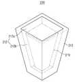
도 1은 본 발명의 몇몇 실시예들에 따른 반도체 장치의 레이아웃도이다.
도 2는 도 1의 컨택 구조체의 평면도이다.
도 3은 도 1의 컨택 구조체의 사시도이다.
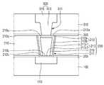
도 4 내지 도 9는 도 1의 A-A' 선을 따라 절단한 단면도이다.1 is a layout diagram of a semiconductor device according to some embodiments of the present invention.
2 is a plan view of the contact structure of FIG.
Figure 3 is a perspective view of the contact structure of Figure 1;
4 to 9 are sectional views taken along the line AA 'in Fig.
다른 정의가 없다면, 본 명세서에서 사용되는 모든 용어(기술 및 과학적 용어를 포함)는 본 발명이 속하는 기술분야에서 통상의 지식을 가진 자에게 공통적으로 이해될 수 있는 의미로 사용될 수 있을 것이다. 또 일반적으로 사용되는 사전에 정의되어 있는 용어들은 명백하게 특별히 정의되어 있지 않는 한 이상적으로 또는 과도하게 해석되지 않는다.Unless defined otherwise, all terms (including technical and scientific terms) used herein may be used in a sense commonly understood by one of ordinary skill in the art to which this invention belongs. Also, commonly used predefined terms are not ideally or excessively interpreted unless explicitly defined otherwise.
이하에서, 도 1 내지 도 5를 참조하여 본 발명의 몇몇 실시예들에 따른 반도체 장치에 대해 설명한다.Hereinafter, a semiconductor device according to some embodiments of the present invention will be described with reference to FIGS. 1 to 5. FIG.
도 1은 본 발명의 몇몇 실시예들에 따른 반도체 장치의 레이아웃도이다. 도 1에서는 도시의 명확성을 위해 층간 절연막의 도시를 생략하였다. 도 2는 도 1의 컨택 구조체의 평면도이다. 도 3은 도 1의 컨택 구조체의 사시도이다. 도 4 및 도 5는 도 1의 A-A' 선을 따라 절단한 단면도이다.1 is a layout diagram of a semiconductor device according to some embodiments of the present invention. In FIG. 1, the illustration of the interlayer insulating film is omitted for the sake of clarity. 2 is a plan view of the contact structure of FIG. Figure 3 is a perspective view of the contact structure of Figure 1; 4 and 5 are sectional views taken along line A-A 'in Fig.
도 1 내지 도 5를 참조하면, 본 발명의 기술적 사상에 따른 반도체 장치는, 하부막(100), 배선(300) 및 컨택 구조체(200)를 포함할 수 있다.1 to 5, a semiconductor device according to the technical idea of the present invention may include a
하부막(100)은, 예를 들어, 기판일 수 있다. 그러나, 본 발명이 이에 제한되는 것은 아니다. 하부막(100)은, 예를 들어, 기판 상에 배치되는 층간 절연막 중 하나일 수 있다.The
하부막(100)은 예를 들어, 벌크 실리콘 또는 SOI(silicon-on-insulator)일 수 있다. 이와 달리, 하부막(100)은 실리콘 기판일 수도 있고, 또는 다른 물질, 예를 들어, 실리콘게르마늄, 안티몬화 인듐, 납 텔루르 화합물, 인듐 비소, 인듐 인화물, 갈륨 비소 또는 안티몬화 갈륨을 포함할 수 있다. 또는, 하부막(100)은 베이스 기판 상에 에피층이 형성된 것일 수도 있다.The
하부막(100)은, 제1 영역(110)을 포함할 수 있다. 제1 영역(110)은, 예를 들어, 하부막(100) 내에 형성되는 트랜지스터의 소오스 또는 드레인일 수 있다. 또는, 제1 영역(110)은, 예를 들어, 하부막(100) 내에 형성되는 트랜지스터의 게이트 전극일 수 있다. 또는, 제1 영역(110)은, 예를 들어, 하부막(100) 내에 형성되는 다이오드 등일 수 있다. 다시 말해서, 제1 영역(110)은, 후술할 배선(300)과 컨택 구조체(200)를 통해 전기적으로 연결시켜야할, 하부막(100) 내에 형성된 회로 요소일 수 있다. 그러나 본 발명이 이에 제한되는 것은 아니다. 예를 들어, 제1 영역(110)은, 회로 요소와 컨택 구조체(200)를 연결시키기 위한 구성 요소일 수도 있다.The
제1 식각 정지막(205)은, 하부막(100) 상에 배치될 수 있다. 제1 식각 정지막(205)은, 예를 들어, 제1 영역(110)의 일부를 덮도록, 제1 영역(110) 상에도 형성될 수 있다. 제1 식각 정지막(205)은, 컨택 구조체(200)를 제1 영역(110)과 접속시키기 위한, 불연속적인 패턴일 수 있다. 예를 들어, 제1 식각 정지막(205)은, 컨택 구조체(200)가 제1 영역(110)과 접속되는 부분에는 형성되지 않을 수 있다. 제1 식각 정지막(205)은, 컨택 트렌치(211) 형성 시, 과도한 식각을 막아, 하부막(100)의 손실을 방지할 수 있다.The first
층간 절연막(210)은, 제1 식각 정지막(205) 상에 배치될 수 있다. 층간 절연막(210)은 배선 사이의 커플링 현상을 경감시키기 위해 예를 들어, 저유전율 물질, 산화막, 질화막 및 산질화막 중 적어도 하나를 포함할 수 있다. 저유전율 물질은 예를 들어, FOX(Flowable Oxide), TOSZ(Tonen SilaZen), USG(Undoped Silica Glass), BSG(Borosilica Glass), PSG(PhosphoSilica Glass), BPSG(BoroPhosphoSilica Glass), PETEOS(Plasma Enhanced Tetra Ethyl Ortho Silicate), FSG(Fluoride Silicate Glass), CDO(Carbon Doped silicon Oxide), Xerogel, Aerogel, Amorphous Fluorinated Carbon, OSG(Organo Silicate Glass), Parylene, BCB(bis-benzocyclobutenes), SiLK, polyimide, porous polymeric material 또는 이들의 조합을 포함할 수 있으나, 이에 제한되는 것은 아니다.The
예를 들어, 층간 절연막(210)은, 제1 식각 정지 막(205)과 식각 선택성을 갖는 물질을 포함할 수 있다.For example, the
층간 절연막(210)은, 컨택 구조체(200)를 포함할 수 있다. 컨택 구조체(200)는, 컨택 트렌치(211), 배리어 막(213), 컨택(219) 및 캡핑 패턴(212)을 포함할 수 있다. 그러나, 본 발명이 이에 제한되는 것은 아니다. 예를 들어, 컨택 구조체(200)는, 필요에 따라, 다른 막을 더 포함할 수 있음은 물론이다.The interlayer
층간 절연막(210)은, 컨택 트렌치(211)를 포함할 수 있다. 컨택 트렌치(211)는, 층간 절연막(210) 내에 배치되어, 층간 절연막(210)을 관통할 수 있다. 컨택 트렌치(211)는, 제1 영역(110)의 적어도 일부를 노출시킬 수 있다.The
도면에서, 컨택 트렌치(211)의 측벽이, 하부막(100)의 상면을 기준으로 임의의 기울기를 갖는 것으로 도시하였으나, 본 발명이 이에 제한되는 것은 아니다. 예를 들어, 컨택 트렌치(211)의 측벽은, 제조 공정에 따라, 하부막(100)의 상면에 대해 수직인 기울기를 가질 수 있음은 물론이다.Although the sidewalls of the
배리어 막(213)은, 컨택 트렌치(211)를 전부 채우지 않을 수 있다.The
배리어 막(213)은, 제1 부분(213-1)과 제2 부분(213-2)을 포함할 수 있다. 배리어 막(213)의 제1 부분(213-1)은, 컨택 트렌치(211)의 양 측벽을 따라 배치되는 부분일 수 있다. 배리어 막(213)의 제1 부분(213-1)은, 컨택 트렌치(211)의 양 측벽을 따라 컨포말하게(conformally) 형성될 수 있다.The
배리어 막(213)의 제2 부분(213-2)은, 컨택 트렌치(211)의 바닥면을 따라 배치되는 부분일 수 있다. 배리어 막(213)의 제2 부분(213-2)은, 컨택 트렌치(211)의 바닥면을 따라 컨포말하게 형성될 수 있다. 배리어 막(213)의 제2 부분(213-2)의 적어도 일부는, 예를 들어, 제1 영역(110) 상에 배치될 수 있다. 몇몇 실시예에서, 배리어 막(213)의 제2 부분(213-2)의 적어도 일부는, 제1 영역(110)과 직접 접할 수 있다.The second portion 213-2 of the
배리어 막(213)은, 후술할 캡핑 막(212a) 상에는 배치되지 않을 수 있다. 다시 말해서, 배리어 막(213)은, 캡핑 패턴(212)의 상면(212U) 상에는 배치되지 않을 수 있다.The
배리어 막(213)은, 예를 들어, 타이타늄 나이트라이드(TiN)를 포함할 수 있다. 그러나, 본 발명이 이에 제한되는 것은 아니다. 예를 들어, 컨택(219)에 포함된 물질이 층간 절연막(210)으로 이동하는 것을 방지시킬 수 있는 물질이라면 배리어 막(213)에 포함될 수 있음은 물론이다.The
컨택(219)은 배리어 막(213)의 제1 부분(213-1)과 이격되도록, 컨택 트렌치(211) 내에 배치될 수 있다. 컨택(219)은, 컨택 트렌치(211)의 일부만을 채울 수 있다. 예를 들어, 하부막(100)의 상면을 기준으로, 컨택(219)의 상면(219U)은, 층간 절연막(210)의 상면(210U) 보다 아래에 있을 수 있다. 컨택(219)의 하면(219L)과 제1 영역(110) 사이에는, 배리어 막(213)의 제2 부분(213-2)이 위치할 수 있다.The
도면에서, 컨택(219)이 컨택 트렌치(211)의 프로파일을 따른 형상을 갖는 것으로 도시하였으나, 본 발명이 이에 제한되는 것은 아니다. 예를 들어, 컨택(219)은, 컨택 트렌치(211)의 일부를 채우고, 배리어 막(213)의 제1 부분(213-1)과 이격되어 컨택 트렌치(211) 내에 배치된다면, 도시된 바와 상이한 형상을 가질 수 있음은 물론이다.Although the
컨택(219)은 예를 들어, 코발트를 포함할 수 있다. 컨택(219)은, 하부막(100)과 후술할 상부막(310)을 전기적으로 연결시킬 수 있다. 구체적으로, 컨택(219)은, 하부막(100)의 제1 영역(110)과, 상부막(310)의 배선(300)을 전기적으로 연결시켜줄 수 있다.The
캡핑 패턴(212)은, 컨택(219)의 둘레를 감싸고, 컨택(219)의 상면(219U)을 덮을 수 있다. 캡핑 패턴(212)은, 컨택(219)의 하면(219L) 상에는 배치되지 않을 수 있다. 캡핑 패턴(212)은, 캡핑 막(212a)과 라이너(212b)를 포함할 수 있다.The
라이너(212b)는, 컨택(219)의 둘레를 감싸는 부분일 수 있다. 또한, 라이너(212b)는, 컨택(219)과 배리어 막(213)의 제1 부분(213-1)이 이격되는 공간에 배치될 수 있다. 다시 말해서, 라이너(212b)는, 컨택 트렌치(211) 내에, 배리어 막(213)의 제1 부분(213-1)과 컨택(219) 사이에 개재될 수 있다. 라이너(212b)는, 예를 들어, 컨택(219)과 배리어 막(213)의 제2 부분(213-2) 사이에는 개재되지 않을 수 있다.The
캡핑 막(212a)은 컨택(219) 및 라이너(212b) 상에 배치되는 부분일 수 있다. 캡핑 막(212a)은, 컨택(219)이 컨택 트렌치(211)의 일부를 채우고 남은 컨택 트렌치(211)의 부분을 채우도록 배치될 수 있다.The
몇몇 실시예에서, 컨택 구조체(200)의 상면인 캡핑 패턴(212)의 상면(212U)은, 층간 절연막(210)의 상면(210U)과 실질적으로 동일 평면 상에 놓일 수 있다. 컨택 구조체(200)는, 층간 절연막(210)을 관통하도록 배치될 수 있다. 다시 말해서, 층간 절연막(210)은, 배리어 막(213)의 둘레를 감싸고, 캡핑 패턴(212)의 상면(212U)을 노출시키도록 배치될 수 있다.In some embodiments, the top surface 212U of the
배리어 막(213)은, 캡핑 패턴(212)의 둘레를 감싸고, 캡핑 패턴(212)의 하면(212L) 및 컨택(219)의 하면(219L)을 덮을 수 있다.The
캡핑 패턴(212)은 산화물(oxide)에 대해 식각 선택성(etch selectivity)을 갖는 물질을 포함할 수 있다. 여기서 식각 선택성은, 산화물을 식각할 수 있는 식각액을 이용하여 산화물을 포함하는 구성 요소에 대한 식각 공정을 수행하는 동안, 캡핑 패턴(212)은 실질적으로 식각되지 않는 것을 의미할 수 있다. 즉, 산화물을 식각할 수 있는 식각액에 대해, 캡핑 패턴(212)이 반응하지 않는 것을 의미할 수 있다. 또한, 반대로, 캡핑 패턴(212)을 식각할 수 있는 식각액을 이용하여 캡핑 패턴(212)에 대한 식각 공정을 수행하는 동안, 산화물을 포함하는 구성요소는 실질적으로 식각되지 않는 것을 의미할 수 있다. 이 때, 산화물을 포함하는 구성 요소는, 예를 들어, 상부막(310)일 수 있다. 캡핑 패턴(212)은, 예를 들어, 루테늄(ruthenium)과 텅스텐(tungsten) 중 어느 하나를 포함할 수 있다.The
본 발명의 기술적 사상에 따른 반도체 장치는, 컨택(219)의 둘레를 감싸고 상면을 덮는 캡핑 패턴(212)을 층간 절연막(210) 내에 배치하고, 캡핑 패턴(212)이 산화물에 대해 식각 선택성을 갖는 물질을 포함하도록 함으로써, 후속 공정에서 발생될 수 있는 컨택(219)의 손실을 현저히 감소시킬 수 있다.The semiconductor device according to the technical idea of the present invention is characterized in that a
구체적으로, 캡핑 패턴(212)이 산화물에 대해 식각 선택성을 갖는 물질을 포함하는 경우, 후속 공정 중 불산(HF) 등을 이용한 식각 공정에서 캡핑 패턴(212)은 실질적으로 거의 식각되지 않을 수 있다. 이 때, 캡핑 패턴(212)이 컨택(219)의 둘레 및 상면을 덮도록 배치되기 때문에, 컨택(219)의 손상 가능성은 현저히 감소될 수 있다. 컨택(219)의 상면뿐만 아니라 둘레까지 감싸는 경우 컨택(219)이 캡핑 패턴(212)에 의해 완전히 보호될 수 있기 때문에, 캡핑 패턴(212)이 컨택(219)의 상면만 덮는 경우에 비해, 후속 공정에서 발생될 수 있는 컨택(219)의 손실 가능성을 현저히 감소시킬 수 있다. 여기서 후속 공정은, 예를 들어, 배선 형성을 위해 상부막(310)을 식각하는 공정 및 세정 공정 등을 포함할 수 있다. 예를 들어, 후술할 배선(300)을 형성하기 위해 산화물을 포함하는 상부막(310)을 식각하는 공정 등에 있어서, 캡핑 패턴(212)은, 산화물에 대한 식각 선택성을 갖는 물질을 포함하기 때문에, 실질적으로 식각되지 않을 수 있다.Specifically, if the
제2 식각 정지막(305)은, 층간 절연막(210) 상에 배치될 수 있다. 제2 식각 정지막(305)은, 캡핑 패턴(212)의 일부를 덮도록, 컨택 구조체(200) 상에도 형성될 수 있다. 제2 식각 정지막(305)은, 배선(300)을 컨택 구조체(200)와 접속시키기 위한, 불연속적인 패턴일 수 있다. 예를 들어, 제2 식각 정지막(305)은, 컨택 구조체(200)가 배선(300)과 접속되는 부분에는 형성되지 않을 수 있다. 제2 식각 정지막(305)은, 비아 홀(311) 형성 시, 과도한 식각을 막아, 컨택 구조체(200) 등의 손실을 방지할 수 있다.The second
도면에서, 제1 식각 정지막(205)과 제2 식각 정지막(305)이 단일 막 구조인 것으로 도시하였으나, 본 발명이 이에 제한되는 것은 아니다. 예를 들어, 제1 식각 정지막(205)과 제2 식각 정지막(305)은, 다중 막 구조일 수 있다.Although the first
상부막(310)은, 제2 식각 정지막(305) 상에 배치될 수 있다. 또한, 상부막(310)은, 컨택 구조체(200)의 캡핑 패턴(212)의 상면(212U) 상에 배치될 수 있다. 이에 따라, 컨택 구조체(200) 및 층간 절연막(210)은, 하부막(100)과 상부막(310) 사이에 배치될 수 있다. 상부막(310)은, 예를 들어, 산화물을 포함할 수 있다.The
본 발명의 기술적 사상에 따른 반도체 장치는, 산화물을 포함하는 상부막(310)을 식각하여 비아 홀(311)을 형성하는 식각 공정에서, 캡핑 패턴(212)이 산화물에 대해 식각 선택성을 갖는 물질을 포함하기 때문에, 캡핑 패턴(212)은 실질적으로 식각되지 않을 수 있다. 이 경우, 캡핑 패턴(212)이 컨택(219)의 둘레 및 상면을 덮도록 배치되기 때문에, 컨택(219)은 비아 홀(311)을 형성하기 위한 상부막(310)의 식각 공정 중, 보호될 수 있다. 이는, 컨택(219) 형성 후, 후속 공정에서 발생될 수 있는 컨택(219)의 손실 가능성을 현저히 감소시킬 수 있다.The semiconductor device according to the technical idea of the present invention is characterized in that in the etching process for forming the via
상부막(310)은 비아 홀(311)과 비아 홀(311) 내부에 배치되는 배선(300)을 포함할 수 있다.The
비아 홀(311)은 상부막(310) 내에 배치될 수 있다. 비아 홀(311)은, 상부막(310)을 관통하여, 캡핑 패턴(212)의 상면(212U)의 적어도 일부를 노출시킬 수 있다. 비아 홀(311)은, 예를 들어, 캡핑 패턴(212)의 상면(212U)만을 노출시키도록 형성될 수 있다. 또는, 도 5에서와 같이, 비아 홀(311)은, 캡핑 패턴(212)의 상면(212U)의 일부와, 층간 절연막(210)의 상면(210U)의 일부를 노출시키도록 형성될 수도 있다.The via
비아 홀(311)에는, 예를 들어, 금속 물질이 채워져, 배선(300)이 형성될 수 있다. 배선(300)은, 상부막(310)을 관통하도록 배치될 수 있다. 배선(300)은, 컨택 구조체(200)를 통해, 하부막(100)의 제1 영역(110)과 전기적으로 연결될 수 있다.The via
비아 홀(311)은, 상부와 하부를 포함할 수 있다.The via
비아 홀(311)의 하부에는, 비아 컨택(313)이 배치될 수 있다. 즉, 비아 홀(311)이 예를 들어, 금속 물질로 채워지는 경우, 비아 홀(311)의 하부에는 비아 컨택(219)이 형성될 수 있다. 비아 컨택(219)의 하면은, 예를 들어, 캡핑 패턴(212)의 상면(212U)의 적어도 일부와 직접 접할 수 있다. 예를 들어, 비아 컨택(219)의 하면은, 캡핑 패턴(212)의 상면(212U)의 일부와 직접 접할 수 있다. 또는, 예를 들어, 비아 컨택(219)의 하면은, 도 5에서와 같이, 캡핑 패턴(212)의 상면(212U)의 일부와 직접 접할 수 있다.A via
비아 홀(311)의 상부에는, 배선 패턴(315)이 배치될 수 있다. 즉, 비아 홀(311)이 예를 들어, 금속 물질로 채워지는 경우, 비아 홀(311)의 상부에는 배선 패턴(315)이 형성될 수 있다. 배선 패턴(315)은 비아 컨택(219)을 통해, 컨택 구조체(200)와 전기적으로 연결될 수 있다.A
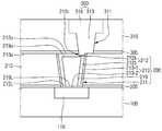
이하에서, 도 1 내지 도 3, 도 6 및 도 7을 참조하여 본 발명의 몇몇 실시예들에 따른 반도체 장치에 대해 설명한다. 설명의 명확성을 위해 앞서 설명한 것과 중복되는 것은 생략한다.Hereinafter, a semiconductor device according to some embodiments of the present invention will be described with reference to FIGS. 1 to 3, 6, and 7. FIG. For the sake of clarity, duplicate descriptions of the above description are omitted.
도 6 및 도 7은 도 1의 A-A' 선을 따라 절단한 단면도이다.6 and 7 are cross-sectional views taken along the line A-A 'in FIG.
도 1 내지 도 3, 도 6 및 도 7을 참조하면, 캡핑 패턴(212)의 상면(212U)은, 층간 절연막(210)의 상면(210U)보다 돌출될 수 있다.Referring to FIGS. 1 to 3, 6 and 7, the upper surface 212U of the
도면에서, 캡핑 패턴(212)의 캡핑 막(212a)에서, 층간 절연막(210)의 상면(210U)보다 돌출된 부분의 모서리가 직각인 것으로 도시하였으나, 이는 예시적인 것일 뿐 본 발명이 이에 제한되는 것은 아니다. 예를 들어, 층간 절연막(210)의 상면(210U)보다 돌출된 캡핑 막(212a)의 부분은, 모따기 형상을 가질 수 있다.Although the edge of the
제2 식각 절연막()은, 층간 절연막(210)의 상면(210U) 및 캡핑 막(212a)의 상면(212U)의 프로파일을 따라 형성될 수 있다.The second etchant insulating film may be formed along the profile of the upper surface 210U of the
캡핑 패턴(212)의 상면(212U)이 층간 절연막(210)의 상면(210U)보다 돌출된 경우에도, 비아 컨택(219)의 하면은, 캡핑 패턴(212)의 상면(212U)의 적어도 일부와 직접 접할 수 있다. 예를 들어, 비아 컨택(219)의 하면은, 캡핑 패턴(212)의 상면(212U)의 일부와 직접 접할 수 있다. 또는, 예를 들어, 비아 컨택(219)의 하면은, 도 7에서와 같이, 캡핑 패턴(212)의 상면(212U)의 일부와 직접 접할 수 있다.Even when the upper surface 212U of the
본 발명의 기술적 사상에 따른 반도체 장치는, 캡핑 막(212b)이 컨택 트렌치(211)의 나머지 일부를 채우면서, 층간 절연막(210)의 상면(210U) 상으로도 돌출되도록 배치하여, 도 7에서와 같이 약간의 정렬 불량(misalignment)이 발생하더라도, 캡핑 막(212b)이 컨택(219)의 상면을 덮을 수 있다. 이는, 후속 공정에서 발생될 수 있는 컨택(219) 손실의 가능성을 현저히 감소시킬 수 있다. 이로써, 반도체 장치의 수율은 향상될 수 있다.The semiconductor device according to the technical idea of the present invention is arranged such that the
이하에서, 도 1 내지 도 3, 도 8 및 도 9를 참조하여 본 발명의 몇몇 실시예들에 따른 반도체 장치에 대해 설명한다. 설명의 명확성을 위해 앞서 설명한 것과 중복되는 것은 생략한다.Hereinafter, a semiconductor device according to some embodiments of the present invention will be described with reference to FIGS. 1 to 3, 8, and 9. FIG. For the sake of clarity, duplicate descriptions of the above description are omitted.
도 8 및 도 9는 도 1의 A-A' 선을 따라 절단한 단면도이다.8 and 9 are cross-sectional views taken along line A-A 'in Fig.
도 1 내지 도 3, 도 8 및 도 9를 참조하면, 캡핑 패턴(212)의 상면(212U)은, 리세스(215r)를 포함할 수 있다. 다시 말해서, 캡핑 막(212a)은, 리세스(215r)를 포함할 수 있다.1 to 3, 8 and 9, the upper surface 212U of the
하부막(100)의 상면을 기준으로, 리세스(215r)의 바닥면은, 컨택(219)의 상면(219U)보다 높게 위치할 수 있다. 하부막(100)의 상면을 기준으로, 리세스(215r)의 바닥면은, 층간 절연막(210)의 상면(210U) 보다 낮게 위치할 수 있다.The bottom surface of the
리세스(215r)는, 비아 컨택(219)에 의해 채워질 수 있다. 다시 말해서, 비아 컨택(219)의 일부는, 캡핑 패턴(212) 내로 삽입될 수 있다. 리세스(215r)의 양 측벽과 바닥면은 모두, 캡핑 막(212a)에 의해 정의될 수 있다. 이 경우, 비아 홀(311)의 하면은, 리세스(215r)의 바닥면에 의해 정의될 수 있다.The
또는, 예를 들어, 도 9의 경우와 같이, 비아 홀(311)의 하면의 일부만 리세스(215r)의 바닥면에 의해 정의될 수 있다. 즉, 리세스(215r)의 일측벽은 배리어 막(213)의 제1 부분(213-1)에 의해 정의되고, 리세스(215r)의 타측벽은 캡핑 막(212a)에 의해 정의될 수 있다. 이 경우, 비아 컨택(219)의 하부의 일부는, 리세스(215r)내로 삽입될 수 있고, 비아 컨택(219)의 하부의 나머지 일부는 배리어 막(213)의 제1 부분(213-1) 상에 배치될 수 있다.Alternatively, for example, as in the case of FIG. 9, only a part of the lower surface of the via
이상 첨부된 도면을 참조하여 본 발명의 실시예들을 설명하였으나, 본 발명은 상기 실시예들에 한정되는 것이 아니라 서로 다른 다양한 형태로 제조될 수 있으며, 본 발명이 속하는 기술분야에서 통상의 지식을 가진 자는 본 발명의 기술적 사상이나 필수적인 특징을 변경하지 않고서 다른 구체적인 형태로 실시될 수 있다는 것을 이해할 수 있을 것이다. 그러므로 이상에서 기술한 실시예들은 모든 면에서 예시적인 것이며 한정적이 아닌 것으로 이해해야만 한다.While the present invention has been described in connection with what is presently considered to be practical exemplary embodiments, it is to be understood that the invention is not limited to the disclosed embodiments, but, on the contrary, It is to be understood that the invention may be embodied in other specific forms without departing from the spirit or essential characteristics thereof. It is therefore to be understood that the above-described embodiments are illustrative in all aspects and not restrictive.
100: 하부막200: 컨택 구조체
211: 컨택 트렌치212: 캡핑 패턴
213: 배리어 막219: 컨택
310: 상부막100: lower layer 200: contact structure
211: contact trench 212: capping pattern
213: barrier film 219: contact
310: Upper film
Claims (10)
Translated fromKorean상기 하부막 상에 배치되는 상부막;
상기 하부막과 상기 상부막 사이에 배치되어 상기 하부막과 상기 상부막을 전기적으로 연결하는 컨택;
상기 컨택의 둘레를 감싸고, 상기 컨택의 상면을 덮는 캡핑 패턴;
상기 캡핑 패턴의 둘레를 감싸고, 상기 캡핑 패턴의 하면 및 상기 컨택의 하면을 덮는 배리어 막; 및
상기 하부막과 상기 상부막 사이에 배치되고, 상기 배리어 막의 둘레를 감싸도록 배치되는 층간 절연막으로, 상기 캡핑 패턴의 상면을 노출시키는 층간 절연막을 포함하고,
상기 캡핑 패턴은, 산화물(oxide)에 대해 식각 선택성을 갖는 물질을 포함하는 반도체 장치.Bottom membrane;
An upper film disposed on the lower film;
A contact disposed between the lower film and the upper film to electrically connect the lower film and the upper film;
A capping pattern surrounding the contact and covering an upper surface of the contact;
A barrier film surrounding the capping pattern and covering the lower surface of the capping pattern and the lower surface of the contact; And
And an interlayer insulating film disposed between the lower film and the upper film and arranged to surround the periphery of the barrier film, the interlayer insulating film exposing an upper surface of the capping pattern,
Wherein the capping pattern comprises a material having an etch selectivity to oxide.
상기 캡핑 패턴은, 루테늄(ruthenium)과 텅스텐(tungsten) 중 어느 하나를 포함하는 반도체 장치.The method according to claim 1,
Wherein the capping pattern comprises one of ruthenium and tungsten.
상기 컨택은, 코발트(cobalt)를 포함하는 반도체 장치.The method according to claim 1,
Wherein the contact comprises a cobalt.
상기 캡핑 패턴의 상기 상면은, 상기 층간 절연막의 상면으로부터 돌출되는 반도체 장치.The method according to claim 1,
And the upper surface of the capping pattern protrudes from the upper surface of the interlayer insulating film.
상기 층간 절연막과 상기 캡핑 패턴의 상기 상면 상에 배치되는 상부막을 더 포함하고,
상기 상부막은,
상기 상부막 내에, 상기 상부막을 관통하여 상기 캡핑 패턴의 상기 상면의 적어도 일부를 노출시키는 비아 홀과, 상기 비아 홀을 채우는 배선을 포함하고,
상기 컨택은, 상기 배선과 상기 하부막을 전기적으로 연결하는 반도체 장치.The method according to claim 1,
Further comprising an interlayer insulating film and an upper film disposed on the upper surface of the capping pattern,
The above-
A via hole exposing at least a part of the upper surface of the capping pattern through the upper film in the upper film, and a wiring filling the via hole,
And the contact electrically connects the wiring and the lower film.
상기 캡핑 패턴의 상기 상면은 리세스를 포함하고,
상기 배선의 일부는 상기 리세스 내로 삽입되는 반도체 장치.6. The method of claim 5,
Wherein the top surface of the capping pattern comprises a recess,
And a part of the wiring is inserted into the recess.
상기 하부막 상에 배치되는 층간 절연막;
상기 층간 절연막 내에 배치되고, 상기 층간 절연막을 관통하여 상기 제1 영역의 적어도 일부를 노출시키는 컨택 트렌치;
상기 컨택 트렌치의 양 측벽을 따라 배치되는 제1 부분과 상기 컨택 트렌치의 바닥면을 따라 배치되는 제2 부분을 포함하는 배리어 막;
상기 컨택 트렌치의 일부를 채우고, 상기 배리어 막의 상기 제1 부분과 이격되어 배치되는 컨택;
상기 컨택 트렌치 내에, 상기 컨택과 상기 배리어 막의 상기 제1 부분 사이에 배치되는 라이너; 및
상기 컨택 및 상기 라이너 상에 배치되고, 상기 컨택 트렌치의 나머지 일부를 채우도록 배치되는 캡핑 막을 포함하고,
상기 캡핑 막과 상기 라이너는 루테늄(ruthenium)과 텅스텐(tungsten) 중 어느 하나를 포함하는 반도체 장치.A lower film including a first region;
An interlayer insulating film disposed on the lower film;
A contact trench disposed in the interlayer insulating film, the contact trench penetrating the interlayer insulating film to expose at least a part of the first region;
A barrier film comprising a first portion disposed along both sidewalls of the contact trench and a second portion disposed along a bottom surface of the contact trench;
A contact that fills a portion of the contact trench and is spaced apart from the first portion of the barrier film;
A liner disposed in the contact trench, the liner disposed between the contact and the first portion of the barrier film; And
And a capping film disposed on the contact and the liner, the capping film disposed to fill the remaining portion of the contact trench,
Wherein the capping film and the liner comprise one of ruthenium and tungsten.
상기 캡핑 막의 상면은, 상기 층간 절연막의 상면으로부터 돌출되는 반도체 장치.8. The method of claim 7,
And an upper surface of the capping film protrudes from an upper surface of the interlayer insulating film.
상기 층간 절연막과 상기 캡핑 막의 상면 상에 배치되는 상부막을 더 포함하고,
상기 상부막은,
상기 상부막 내에, 상기 상부막을 관통하여 상기 캡핑 막의 상기 상면의 적어도 일부를 노출시키는 비아 홀과, 상기 비아 홀을 채우는 배선을 포함하는 반도체 장치.8. The method of claim 7,
And an upper film disposed on the upper surface of the interlayer insulating film and the capping film,
The above-
A via hole exposing at least a part of the upper surface of the capping film through the upper film in the upper film; and a wiring filling the via hole.
상기 캡핑 막의 상면은 리세스를 포함하고,
상기 배선의 일부는 상기 리세스 내로 삽입되는 반도체 장치.10. The method of claim 9,
Wherein an upper surface of the capping film comprises a recess,
And a part of the wiring is inserted into the recess.
Priority Applications (2)
| Application Number | Priority Date | Filing Date | Title |
|---|---|---|---|
| KR1020160170446AKR102777131B1 (en) | 2016-12-14 | 2016-12-14 | Semiconductor device |
| US15/668,029US10388563B2 (en) | 2016-12-14 | 2017-08-03 | Semiconductor device |
Applications Claiming Priority (1)
| Application Number | Priority Date | Filing Date | Title |
|---|---|---|---|
| KR1020160170446AKR102777131B1 (en) | 2016-12-14 | 2016-12-14 | Semiconductor device |
Publications (2)
| Publication Number | Publication Date |
|---|---|
| KR20180068595Atrue KR20180068595A (en) | 2018-06-22 |
| KR102777131B1 KR102777131B1 (en) | 2025-03-05 |
Family
ID=62489624
Family Applications (1)
| Application Number | Title | Priority Date | Filing Date |
|---|---|---|---|
| KR1020160170446AActiveKR102777131B1 (en) | 2016-12-14 | 2016-12-14 | Semiconductor device |
Country Status (2)
| Country | Link |
|---|---|
| US (1) | US10388563B2 (en) |
| KR (1) | KR102777131B1 (en) |
Cited By (2)
| Publication number | Priority date | Publication date | Assignee | Title |
|---|---|---|---|---|
| KR20200137060A (en)* | 2019-05-28 | 2020-12-09 | 삼성전자주식회사 | Semiconductor device comprising a through via and Method of fabricating the same |
| KR20220009014A (en)* | 2020-07-15 | 2022-01-24 | 삼성전자주식회사 | Semiconductor device and method for fabricating the same |
Families Citing this family (3)
| Publication number | Priority date | Publication date | Assignee | Title |
|---|---|---|---|---|
| CN112309956B (en)* | 2019-07-31 | 2024-10-22 | 中芯国际集成电路制造(上海)有限公司 | Semiconductor structure and forming method thereof |
| US11430735B2 (en)* | 2020-02-14 | 2022-08-30 | International Business Machines Corporation | Barrier removal for conductor in top via integration scheme |
| US12266605B2 (en)* | 2021-09-28 | 2025-04-01 | International Business Machines Corporation | Top via interconnects with line wiggling prevention |
Citations (5)
| Publication number | Priority date | Publication date | Assignee | Title |
|---|---|---|---|---|
| US6323554B1 (en)* | 1992-02-26 | 2001-11-27 | International Business Machines Corporation | Refractory metal capped low resistivity metal conductor lines and vias formed using PVD and CVD |
| KR20080059278A (en)* | 2005-09-30 | 2008-06-26 | 어드밴스드 마이크로 디바이시즈, 인코포레이티드 | Techniques for forming a copper-based metallization layer comprising a conductive capping layer |
| WO2015092780A1 (en)* | 2013-12-20 | 2015-06-25 | Intel Corporation | Cobalt based interconnects and methods of fabrication thereof |
| KR20150081620A (en)* | 2014-01-06 | 2015-07-15 | 삼성전자주식회사 | Methods of forming wiring structures and methods of manufacturing semiconductor devices |
| KR20160116618A (en)* | 2015-03-30 | 2016-10-10 | 삼성전자주식회사 | A semiconductor device and method of manufacturing the semiconductor device |
Family Cites Families (35)
| Publication number | Priority date | Publication date | Assignee | Title |
|---|---|---|---|---|
| JPH05102155A (en)* | 1991-10-09 | 1993-04-23 | Sony Corp | Copper wiring structure and its manufacture |
| GB9219281D0 (en)* | 1992-09-11 | 1992-10-28 | Inmos Ltd | Manufacture of semiconductor devices |
| JP3297220B2 (en)* | 1993-10-29 | 2002-07-02 | 株式会社東芝 | Semiconductor device manufacturing method and semiconductor device |
| EP0720228B1 (en)* | 1994-12-29 | 2002-07-10 | STMicroelectronics, Inc. | Method of making a semiconductor connection structure |
| US5814560A (en)* | 1995-11-29 | 1998-09-29 | Advanced Micro Devices, Inc. | Metallization sidewall passivation technology for deep sub-half micrometer IC applications |
| US6077774A (en)* | 1996-03-29 | 2000-06-20 | Texas Instruments Incorporated | Method of forming ultra-thin and conformal diffusion barriers encapsulating copper |
| US5913147A (en)* | 1997-01-21 | 1999-06-15 | Advanced Micro Devices, Inc. | Method for fabricating copper-aluminum metallization |
| JP3285509B2 (en)* | 1997-03-18 | 2002-05-27 | 三菱電機株式会社 | Semiconductor device |
| US6355983B2 (en)* | 1997-05-20 | 2002-03-12 | Texas Instruments Incorporated | Surface modified interconnects |
| US6100184A (en)* | 1997-08-20 | 2000-08-08 | Sematech, Inc. | Method of making a dual damascene interconnect structure using low dielectric constant material for an inter-level dielectric layer |
| TW350133B (en)* | 1998-02-06 | 1999-01-11 | United Microelectronics Corp | Method of formation of on-line in copper |
| JPH11354637A (en)* | 1998-06-11 | 1999-12-24 | Oki Electric Ind Co Ltd | Connection structure for wiring and formation of connection part of the wiring |
| US6268261B1 (en)* | 1998-11-03 | 2001-07-31 | International Business Machines Corporation | Microprocessor having air as a dielectric and encapsulated lines and process for manufacture |
| US6734559B1 (en)* | 1999-09-17 | 2004-05-11 | Advanced Micro Devices, Inc. | Self-aligned semiconductor interconnect barrier and manufacturing method therefor |
| US6498364B1 (en)* | 2000-01-21 | 2002-12-24 | Agere Systems Inc. | Capacitor for integration with copper damascene processes |
| US6413788B1 (en)* | 2001-02-28 | 2002-07-02 | Micron Technology, Inc. | Keepers for MRAM electrodes |
| US6680106B1 (en)* | 2001-11-08 | 2004-01-20 | Seagate Technology Llc | Magnetic recording media with Ru corrosion barrier layer |
| US6723635B1 (en)* | 2002-04-04 | 2004-04-20 | Advanced Micro Devices, Inc. | Protection low-k ILD during damascene processing with thin liner |
| JP2004039916A (en)* | 2002-07-04 | 2004-02-05 | Nec Electronics Corp | Semiconductor device and its manufacturing method |
| WO2004107434A1 (en)* | 2003-05-29 | 2004-12-09 | Nec Corporation | Wiring structure and method for producing same |
| US7008871B2 (en)* | 2003-07-03 | 2006-03-07 | International Business Machines Corporation | Selective capping of copper wiring |
| US7157795B1 (en)* | 2004-09-07 | 2007-01-02 | Advanced Micro Devices, Inc. | Composite tantalum nitride/tantalum copper capping layer |
| US7405154B2 (en) | 2006-03-24 | 2008-07-29 | International Business Machines Corporation | Structure and method of forming electrodeposited contacts |
| US20090289370A1 (en) | 2008-05-21 | 2009-11-26 | Advanced Micro Devices, Inc. | Low contact resistance semiconductor devices and methods for fabricating the same |
| US9330939B2 (en) | 2012-03-28 | 2016-05-03 | Applied Materials, Inc. | Method of enabling seamless cobalt gap-fill |
| US9514983B2 (en) | 2012-12-28 | 2016-12-06 | Intel Corporation | Cobalt based interconnects and methods of fabrication thereof |
| US9209073B2 (en) | 2013-03-12 | 2015-12-08 | Taiwan Semiconductor Manufacturing Company, Ltd. | Metal cap apparatus and method |
| US9040421B2 (en) | 2013-05-03 | 2015-05-26 | GlobalFoundries, Inc. | Methods for fabricating integrated circuits with improved contact structures |
| US9287170B2 (en) | 2013-11-27 | 2016-03-15 | Taiwan Semiconductor Manufacturing Company Limited | Contact structure and formation thereof |
| KR102177702B1 (en) | 2014-02-03 | 2020-11-11 | 삼성전자주식회사 | Via Structures and Semiconductor Devices Having a Via plug |
| US10079174B2 (en) | 2014-04-30 | 2018-09-18 | Taiwan Semiconductor Manufacturing Company, Ltd. | Composite contact plug structure and method of making same |
| KR102264160B1 (en) | 2014-12-03 | 2021-06-11 | 삼성전자주식회사 | Method of Fabricating Semiconductor Devices Having Via Structures and Interconnection Structures |
| US9859218B1 (en)* | 2016-09-19 | 2018-01-02 | International Business Machines Corporation | Selective surface modification of interconnect structures |
| US9905513B1 (en)* | 2016-10-24 | 2018-02-27 | International Business Machines Corporation | Selective blocking boundary placement for circuit locations requiring electromigration short-length |
| US9859219B1 (en)* | 2017-01-24 | 2018-01-02 | International Business Machines Corporation | Copper wiring structures with copper titanium encapsulation |
- 2016
- 2016-12-14KRKR1020160170446Apatent/KR102777131B1/enactiveActive
- 2017
- 2017-08-03USUS15/668,029patent/US10388563B2/enactiveActive
Patent Citations (5)
| Publication number | Priority date | Publication date | Assignee | Title |
|---|---|---|---|---|
| US6323554B1 (en)* | 1992-02-26 | 2001-11-27 | International Business Machines Corporation | Refractory metal capped low resistivity metal conductor lines and vias formed using PVD and CVD |
| KR20080059278A (en)* | 2005-09-30 | 2008-06-26 | 어드밴스드 마이크로 디바이시즈, 인코포레이티드 | Techniques for forming a copper-based metallization layer comprising a conductive capping layer |
| WO2015092780A1 (en)* | 2013-12-20 | 2015-06-25 | Intel Corporation | Cobalt based interconnects and methods of fabrication thereof |
| KR20150081620A (en)* | 2014-01-06 | 2015-07-15 | 삼성전자주식회사 | Methods of forming wiring structures and methods of manufacturing semiconductor devices |
| KR20160116618A (en)* | 2015-03-30 | 2016-10-10 | 삼성전자주식회사 | A semiconductor device and method of manufacturing the semiconductor device |
Cited By (4)
| Publication number | Priority date | Publication date | Assignee | Title |
|---|---|---|---|---|
| KR20200137060A (en)* | 2019-05-28 | 2020-12-09 | 삼성전자주식회사 | Semiconductor device comprising a through via and Method of fabricating the same |
| US11791211B2 (en) | 2019-05-28 | 2023-10-17 | Samsung Electronics Co., Ltd. | Semiconductor devices including through vias and methods of fabricating the same |
| KR20220009014A (en)* | 2020-07-15 | 2022-01-24 | 삼성전자주식회사 | Semiconductor device and method for fabricating the same |
| US12426227B2 (en) | 2020-07-15 | 2025-09-23 | Samsung Electronics Co., Ltd. | Method of manufacturing a semiconductor device having a node capping pattern and a gate capping pattern |
Also Published As
| Publication number | Publication date |
|---|---|
| US20180166334A1 (en) | 2018-06-14 |
| KR102777131B1 (en) | 2025-03-05 |
| US10388563B2 (en) | 2019-08-20 |
Similar Documents
| Publication | Publication Date | Title |
|---|---|---|
| US12142558B2 (en) | Semiconductor device | |
| US12362280B2 (en) | Semiconductor device and method of manufacturing the same | |
| US11705386B2 (en) | Semiconductor device including TSV and method of manufacturing the same | |
| US10204825B2 (en) | Semiconductor device having air gap spacers and method for fabricating the same | |
| CN110299321B (en) | Semiconductor device including self-aligned contacts and method of manufacturing the same | |
| KR20180068595A (en) | Semiconductor device | |
| US9559002B2 (en) | Methods of fabricating semiconductor devices with blocking layer patterns | |
| US20200203351A1 (en) | Memory device | |
| KR102201092B1 (en) | Method for fabricating semiconductor device | |
| KR20170031469A (en) | Semiconductor device having supporters and method of fabricating the same | |
| CN106033741A (en) | Metal internal connection structure and its making method | |
| KR20180103397A (en) | Integrated circuit device | |
| US20220254880A1 (en) | Semiconductor devices having gate isolation layers | |
| US11562974B2 (en) | Hybrid bonding structure and method of fabricating the same | |
| US8034714B2 (en) | Semiconductor device and method of fabricating the same | |
| CN223231510U (en) | semiconductor structure | |
| CN109962052A (en) | Semiconductor device including landing pad | |
| JP2013229503A (en) | Semiconductor device and method of manufacturing the same | |
| KR20220168854A (en) | Semiconductor device | |
| KR102766439B1 (en) | Method of forming a wiring structure | |
| KR20220170676A (en) | Semiconductor device | |
| KR100776141B1 (en) | Metal wiring formation method of semiconductor device | |
| CN119153528A (en) | Semiconductor structure and manufacturing method thereof |
Legal Events
| Date | Code | Title | Description |
|---|---|---|---|
| PA0109 | Patent application | Patent event code:PA01091R01D Comment text:Patent Application Patent event date:20161214 | |
| PG1501 | Laying open of application | ||
| PA0201 | Request for examination | Patent event code:PA02012R01D Patent event date:20211210 Comment text:Request for Examination of Application Patent event code:PA02011R01I Patent event date:20161214 Comment text:Patent Application | |
| E902 | Notification of reason for refusal | ||
| PE0902 | Notice of grounds for rejection | Comment text:Notification of reason for refusal Patent event date:20231025 Patent event code:PE09021S01D | |
| PE0902 | Notice of grounds for rejection | Comment text:Final Notice of Reason for Refusal Patent event date:20240625 Patent event code:PE09021S02D | |
| E701 | Decision to grant or registration of patent right | ||
| PE0701 | Decision of registration | Patent event code:PE07011S01D Comment text:Decision to Grant Registration Patent event date:20250226 | |
| GRNT | Written decision to grant | ||
| PR0701 | Registration of establishment | Comment text:Registration of Establishment Patent event date:20250228 Patent event code:PR07011E01D | |
| PR1002 | Payment of registration fee | Payment date:20250228 End annual number:3 Start annual number:1 | |
| PG1601 | Publication of registration |