KR20180030286A - Display device having test unit - Google Patents
Display device having test unitDownload PDFInfo
- Publication number
- KR20180030286A KR20180030286AKR1020160117272AKR20160117272AKR20180030286AKR 20180030286 AKR20180030286 AKR 20180030286AKR 1020160117272 AKR1020160117272 AKR 1020160117272AKR 20160117272 AKR20160117272 AKR 20160117272AKR 20180030286 AKR20180030286 AKR 20180030286A
- Authority
- KR
- South Korea
- Prior art keywords
- semiconductor layer
- test
- electrode
- display device
- gate electrode
- Prior art date
- Legal status (The legal status is an assumption and is not a legal conclusion. Google has not performed a legal analysis and makes no representation as to the accuracy of the status listed.)
- Granted
Links
- 238000012360testing methodMethods0.000titleclaimsabstractdescription269
- 239000004065semiconductorSubstances0.000claimsabstractdescription235
- 239000000758substrateSubstances0.000claimsabstractdescription40
- XUIMIQQOPSSXEZ-UHFFFAOYSA-NSiliconChemical compound[Si]XUIMIQQOPSSXEZ-UHFFFAOYSA-N0.000claimsabstractdescription27
- 229910052710siliconInorganic materials0.000claimsabstractdescription27
- 239000010703siliconSubstances0.000claimsabstractdescription27
- 239000010408filmSubstances0.000claimsdescription120
- 239000010409thin filmSubstances0.000claimsdescription62
- 238000000034methodMethods0.000claimsdescription30
- 239000004973liquid crystal related substanceSubstances0.000claimsdescription13
- 230000007547defectEffects0.000claimsdescription10
- 229910021419crystalline siliconInorganic materials0.000claimsdescription3
- HRHKULZDDYWVBE-UHFFFAOYSA-Nindium;oxozinc;tinChemical compound[In].[Sn].[Zn]=OHRHKULZDDYWVBE-UHFFFAOYSA-N0.000claimsdescription2
- 239000010410layerSubstances0.000description240
- 230000008569processEffects0.000description20
- 239000000463materialSubstances0.000description15
- 239000004698PolyethyleneSubstances0.000description10
- 239000011229interlayerSubstances0.000description10
- 239000003990capacitorSubstances0.000description9
- 230000002950deficientEffects0.000description7
- 230000008439repair processEffects0.000description7
- 125000006850spacer groupChemical group0.000description7
- 238000005538encapsulationMethods0.000description6
- 230000008054signal transmissionEffects0.000description6
- 239000010936titaniumSubstances0.000description6
- XLOMVQKBTHCTTD-UHFFFAOYSA-NZinc monoxideChemical compound[Zn]=OXLOMVQKBTHCTTD-UHFFFAOYSA-N0.000description5
- 229910052751metalInorganic materials0.000description5
- 239000002184metalSubstances0.000description5
- 239000011368organic materialSubstances0.000description5
- 238000007789sealingMethods0.000description5
- VYPSYNLAJGMNEJ-UHFFFAOYSA-Nsilicon dioxideInorganic materialsO=[Si]=OVYPSYNLAJGMNEJ-UHFFFAOYSA-N0.000description5
- 229910052814silicon oxideInorganic materials0.000description5
- ZOKXTWBITQBERF-UHFFFAOYSA-NMolybdenumChemical compound[Mo]ZOKXTWBITQBERF-UHFFFAOYSA-N0.000description4
- RTAQQCXQSZGOHL-UHFFFAOYSA-NTitaniumChemical compound[Ti]RTAQQCXQSZGOHL-UHFFFAOYSA-N0.000description4
- 229910052782aluminiumInorganic materials0.000description4
- XAGFODPZIPBFFR-UHFFFAOYSA-NaluminiumChemical compound[Al]XAGFODPZIPBFFR-UHFFFAOYSA-N0.000description4
- QVGXLLKOCUKJST-UHFFFAOYSA-Natomic oxygenChemical compound[O]QVGXLLKOCUKJST-UHFFFAOYSA-N0.000description4
- 239000011651chromiumSubstances0.000description4
- 239000003086colorantSubstances0.000description4
- 229910052750molybdenumInorganic materials0.000description4
- 239000011733molybdenumSubstances0.000description4
- 229910052760oxygenInorganic materials0.000description4
- 239000001301oxygenSubstances0.000description4
- 229910021420polycrystalline siliconInorganic materials0.000description4
- 229910052719titaniumInorganic materials0.000description4
- 229910000838Al alloyInorganic materials0.000description3
- VYZAMTAEIAYCRO-UHFFFAOYSA-NChromiumChemical compound[Cr]VYZAMTAEIAYCRO-UHFFFAOYSA-N0.000description3
- 229910001182Mo alloyInorganic materials0.000description3
- 229910052804chromiumInorganic materials0.000description3
- 239000010949copperSubstances0.000description3
- 239000012535impuritySubstances0.000description3
- 230000002093peripheral effectEffects0.000description3
- RYGMFSIKBFXOCR-UHFFFAOYSA-NCopperChemical compound[Cu]RYGMFSIKBFXOCR-UHFFFAOYSA-N0.000description2
- -1Si 3 N 4Inorganic materials0.000description2
- 229910052581Si3N4Inorganic materials0.000description2
- 229910004205SiNXInorganic materials0.000description2
- BQCADISMDOOEFD-UHFFFAOYSA-NSilverChemical compound[Ag]BQCADISMDOOEFD-UHFFFAOYSA-N0.000description2
- 238000000231atomic layer depositionMethods0.000description2
- 238000005229chemical vapour depositionMethods0.000description2
- 229910052802copperInorganic materials0.000description2
- 238000001514detection methodMethods0.000description2
- 238000013100final testMethods0.000description2
- 239000011521glassSubstances0.000description2
- 238000002347injectionMethods0.000description2
- 239000007924injectionSubstances0.000description2
- 239000011810insulating materialSubstances0.000description2
- 238000004519manufacturing processMethods0.000description2
- 239000011159matrix materialSubstances0.000description2
- 230000000149penetrating effectEffects0.000description2
- 230000000704physical effectEffects0.000description2
- 239000002861polymer materialSubstances0.000description2
- 230000001681protective effectEffects0.000description2
- 239000003870refractory metalSubstances0.000description2
- 230000004044responseEffects0.000description2
- HQVNEWCFYHHQES-UHFFFAOYSA-Nsilicon nitrideChemical compoundN12[Si]34N5[Si]62N3[Si]51N64HQVNEWCFYHHQES-UHFFFAOYSA-N0.000description2
- 229910052709silverInorganic materials0.000description2
- 239000004332silverSubstances0.000description2
- 238000003860storageMethods0.000description2
- 229910052715tantalumInorganic materials0.000description2
- GUVRBAGPIYLISA-UHFFFAOYSA-Ntantalum atomChemical compound[Ta]GUVRBAGPIYLISA-UHFFFAOYSA-N0.000description2
- 238000002207thermal evaporationMethods0.000description2
- 239000011787zinc oxideSubstances0.000description2
- 239000004925Acrylic resinSubstances0.000description1
- 229920000178Acrylic resinPolymers0.000description1
- 229910001316Ag alloyInorganic materials0.000description1
- 229910018072Al 2 O 3Inorganic materials0.000description1
- 229910017083AlNInorganic materials0.000description1
- 229910017109AlONInorganic materials0.000description1
- GYHNNYVSQQEPJS-UHFFFAOYSA-NGalliumChemical compound[Ga]GYHNNYVSQQEPJS-UHFFFAOYSA-N0.000description1
- 239000004642PolyimideSubstances0.000description1
- 229910004298SiO 2Inorganic materials0.000description1
- 229910010413TiO 2Inorganic materials0.000description1
- ATJFFYVFTNAWJD-UHFFFAOYSA-NTinChemical compound[Sn]ATJFFYVFTNAWJD-UHFFFAOYSA-N0.000description1
- GEIAQOFPUVMAGM-UHFFFAOYSA-NZrOInorganic materials[Zr]=OGEIAQOFPUVMAGM-UHFFFAOYSA-N0.000description1
- 230000032683agingEffects0.000description1
- 229910045601alloyInorganic materials0.000description1
- 239000000956alloySubstances0.000description1
- 229910002064alloy oxideInorganic materials0.000description1
- 229910021417amorphous siliconInorganic materials0.000description1
- 230000015572biosynthetic processEffects0.000description1
- 230000000903blocking effectEffects0.000description1
- 239000000919ceramicSubstances0.000description1
- 239000004020conductorSubstances0.000description1
- 238000005520cutting processMethods0.000description1
- ZGHDMISTQPRNRG-UHFFFAOYSA-NdimolybdenumChemical compound[Mo]#[Mo]ZGHDMISTQPRNRG-UHFFFAOYSA-N0.000description1
- 230000005684electric fieldEffects0.000description1
- 239000003822epoxy resinSubstances0.000description1
- 230000005281excited stateEffects0.000description1
- 229910052733galliumInorganic materials0.000description1
- 230000005283ground stateEffects0.000description1
- 229910052738indiumInorganic materials0.000description1
- APFVFJFRJDLVQX-UHFFFAOYSA-Nindium atomChemical compound[In]APFVFJFRJDLVQX-UHFFFAOYSA-N0.000description1
- 229910003437indium oxideInorganic materials0.000description1
- PJXISJQVUVHSOJ-UHFFFAOYSA-Nindium(iii) oxideChemical compound[O-2].[O-2].[O-2].[In+3].[In+3]PJXISJQVUVHSOJ-UHFFFAOYSA-N0.000description1
- 229910010272inorganic materialInorganic materials0.000description1
- 239000011147inorganic materialSubstances0.000description1
- 150000002739metalsChemical class0.000description1
- 238000012986modificationMethods0.000description1
- 230000004048modificationEffects0.000description1
- 238000001579optical reflectometryMethods0.000description1
- 239000012044organic layerSubstances0.000description1
- NQBRDZOHGALQCB-UHFFFAOYSA-NoxoindiumChemical compound[O].[In]NQBRDZOHGALQCB-UHFFFAOYSA-N0.000description1
- KYKLWYKWCAYAJY-UHFFFAOYSA-Noxotin;zincChemical compound[Zn].[Sn]=OKYKLWYKWCAYAJY-UHFFFAOYSA-N0.000description1
- 230000035515penetrationEffects0.000description1
- 239000004033plasticSubstances0.000description1
- 229920003023plasticPolymers0.000description1
- 229920000647polyepoxidePolymers0.000description1
- 229920000573polyethylenePolymers0.000description1
- 229920001721polyimidePolymers0.000description1
- 229920006254polymer filmPolymers0.000description1
- 239000010453quartzSubstances0.000description1
- 239000011342resin compositionSubstances0.000description1
- 230000035882stressEffects0.000description1
- 230000001629suppressionEffects0.000description1
- JBQYATWDVHIOAR-UHFFFAOYSA-NtellanylidenegermaniumChemical compound[Te]=[Ge]JBQYATWDVHIOAR-UHFFFAOYSA-N0.000description1
- 229910001887tin oxideInorganic materials0.000description1
- 238000002834transmittanceMethods0.000description1
- YVTHLONGBIQYBO-UHFFFAOYSA-Nzinc indium(3+) oxygen(2-)Chemical compound[O--].[Zn++].[In+3]YVTHLONGBIQYBO-UHFFFAOYSA-N0.000description1
Images


Classifications
- H01L51/0031—
- H—ELECTRICITY
- H01—ELECTRIC ELEMENTS
- H01L—SEMICONDUCTOR DEVICES NOT COVERED BY CLASS H10
- H01L22/00—Testing or measuring during manufacture or treatment; Reliability measurements, i.e. testing of parts without further processing to modify the parts as such; Structural arrangements therefor
- H01L22/30—Structural arrangements specially adapted for testing or measuring during manufacture or treatment, or specially adapted for reliability measurements
- H01L22/34—Circuits for electrically characterising or monitoring manufacturing processes, e. g. whole test die, wafers filled with test structures, on-board-devices incorporated on each die, process control monitors or pad structures thereof, devices in scribe line
- H—ELECTRICITY
- H10—SEMICONDUCTOR DEVICES; ELECTRIC SOLID-STATE DEVICES NOT OTHERWISE PROVIDED FOR
- H10K—ORGANIC ELECTRIC SOLID-STATE DEVICES
- H10K71/00—Manufacture or treatment specially adapted for the organic devices covered by this subclass
- H10K71/70—Testing, e.g. accelerated lifetime tests
- G—PHYSICS
- G09—EDUCATION; CRYPTOGRAPHY; DISPLAY; ADVERTISING; SEALS
- G09G—ARRANGEMENTS OR CIRCUITS FOR CONTROL OF INDICATING DEVICES USING STATIC MEANS TO PRESENT VARIABLE INFORMATION
- G09G3/00—Control arrangements or circuits, of interest only in connection with visual indicators other than cathode-ray tubes
- G09G3/006—Electronic inspection or testing of displays and display drivers, e.g. of LED or LCD displays
- H—ELECTRICITY
- H01—ELECTRIC ELEMENTS
- H01L—SEMICONDUCTOR DEVICES NOT COVERED BY CLASS H10
- H01L22/00—Testing or measuring during manufacture or treatment; Reliability measurements, i.e. testing of parts without further processing to modify the parts as such; Structural arrangements therefor
- H01L22/30—Structural arrangements specially adapted for testing or measuring during manufacture or treatment, or specially adapted for reliability measurements
- H01L27/1225—
- H01L27/1251—
- H01L27/3276—
- H01L51/56—
- H—ELECTRICITY
- H10—SEMICONDUCTOR DEVICES; ELECTRIC SOLID-STATE DEVICES NOT OTHERWISE PROVIDED FOR
- H10D—INORGANIC ELECTRIC SEMICONDUCTOR DEVICES
- H10D30/00—Field-effect transistors [FET]
- H10D30/60—Insulated-gate field-effect transistors [IGFET]
- H10D30/67—Thin-film transistors [TFT]
- H10D30/6729—Thin-film transistors [TFT] characterised by the electrodes
- H10D30/673—Thin-film transistors [TFT] characterised by the electrodes characterised by the shapes, relative sizes or dispositions of the gate electrodes
- H10D30/6733—Multi-gate TFTs
- H10D30/6734—Multi-gate TFTs having gate electrodes arranged on both top and bottom sides of the channel, e.g. dual-gate TFTs
- H—ELECTRICITY
- H10—SEMICONDUCTOR DEVICES; ELECTRIC SOLID-STATE DEVICES NOT OTHERWISE PROVIDED FOR
- H10D—INORGANIC ELECTRIC SEMICONDUCTOR DEVICES
- H10D30/00—Field-effect transistors [FET]
- H10D30/60—Insulated-gate field-effect transistors [IGFET]
- H10D30/67—Thin-film transistors [TFT]
- H10D30/674—Thin-film transistors [TFT] characterised by the active materials
- H10D30/6741—Group IV materials, e.g. germanium or silicon carbide
- H10D30/6743—Silicon
- H10D30/6745—Polycrystalline or microcrystalline silicon
- H—ELECTRICITY
- H10—SEMICONDUCTOR DEVICES; ELECTRIC SOLID-STATE DEVICES NOT OTHERWISE PROVIDED FOR
- H10D—INORGANIC ELECTRIC SEMICONDUCTOR DEVICES
- H10D30/00—Field-effect transistors [FET]
- H10D30/60—Insulated-gate field-effect transistors [IGFET]
- H10D30/67—Thin-film transistors [TFT]
- H10D30/674—Thin-film transistors [TFT] characterised by the active materials
- H10D30/6755—Oxide semiconductors, e.g. zinc oxide, copper aluminium oxide or cadmium stannate
- H—ELECTRICITY
- H10—SEMICONDUCTOR DEVICES; ELECTRIC SOLID-STATE DEVICES NOT OTHERWISE PROVIDED FOR
- H10D—INORGANIC ELECTRIC SEMICONDUCTOR DEVICES
- H10D30/00—Field-effect transistors [FET]
- H10D30/60—Insulated-gate field-effect transistors [IGFET]
- H10D30/67—Thin-film transistors [TFT]
- H10D30/6757—Thin-film transistors [TFT] characterised by the structure of the channel, e.g. transverse or longitudinal shape or doping profile
- H—ELECTRICITY
- H10—SEMICONDUCTOR DEVICES; ELECTRIC SOLID-STATE DEVICES NOT OTHERWISE PROVIDED FOR
- H10D—INORGANIC ELECTRIC SEMICONDUCTOR DEVICES
- H10D62/00—Semiconductor bodies, or regions thereof, of devices having potential barriers
- H10D62/80—Semiconductor bodies, or regions thereof, of devices having potential barriers characterised by the materials
- H—ELECTRICITY
- H10—SEMICONDUCTOR DEVICES; ELECTRIC SOLID-STATE DEVICES NOT OTHERWISE PROVIDED FOR
- H10D—INORGANIC ELECTRIC SEMICONDUCTOR DEVICES
- H10D86/00—Integrated devices formed in or on insulating or conducting substrates, e.g. formed in silicon-on-insulator [SOI] substrates or on stainless steel or glass substrates
- H10D86/40—Integrated devices formed in or on insulating or conducting substrates, e.g. formed in silicon-on-insulator [SOI] substrates or on stainless steel or glass substrates characterised by multiple TFTs
- H10D86/421—Integrated devices formed in or on insulating or conducting substrates, e.g. formed in silicon-on-insulator [SOI] substrates or on stainless steel or glass substrates characterised by multiple TFTs having a particular composition, shape or crystalline structure of the active layer
- H10D86/423—Integrated devices formed in or on insulating or conducting substrates, e.g. formed in silicon-on-insulator [SOI] substrates or on stainless steel or glass substrates characterised by multiple TFTs having a particular composition, shape or crystalline structure of the active layer comprising semiconductor materials not belonging to the Group IV, e.g. InGaZnO
- H—ELECTRICITY
- H10—SEMICONDUCTOR DEVICES; ELECTRIC SOLID-STATE DEVICES NOT OTHERWISE PROVIDED FOR
- H10D—INORGANIC ELECTRIC SEMICONDUCTOR DEVICES
- H10D86/00—Integrated devices formed in or on insulating or conducting substrates, e.g. formed in silicon-on-insulator [SOI] substrates or on stainless steel or glass substrates
- H10D86/40—Integrated devices formed in or on insulating or conducting substrates, e.g. formed in silicon-on-insulator [SOI] substrates or on stainless steel or glass substrates characterised by multiple TFTs
- H10D86/441—Interconnections, e.g. scanning lines
- H—ELECTRICITY
- H10—SEMICONDUCTOR DEVICES; ELECTRIC SOLID-STATE DEVICES NOT OTHERWISE PROVIDED FOR
- H10D—INORGANIC ELECTRIC SEMICONDUCTOR DEVICES
- H10D86/00—Integrated devices formed in or on insulating or conducting substrates, e.g. formed in silicon-on-insulator [SOI] substrates or on stainless steel or glass substrates
- H10D86/40—Integrated devices formed in or on insulating or conducting substrates, e.g. formed in silicon-on-insulator [SOI] substrates or on stainless steel or glass substrates characterised by multiple TFTs
- H10D86/471—Integrated devices formed in or on insulating or conducting substrates, e.g. formed in silicon-on-insulator [SOI] substrates or on stainless steel or glass substrates characterised by multiple TFTs having different architectures, e.g. having both top-gate and bottom-gate TFTs
- H—ELECTRICITY
- H10—SEMICONDUCTOR DEVICES; ELECTRIC SOLID-STATE DEVICES NOT OTHERWISE PROVIDED FOR
- H10D—INORGANIC ELECTRIC SEMICONDUCTOR DEVICES
- H10D86/00—Integrated devices formed in or on insulating or conducting substrates, e.g. formed in silicon-on-insulator [SOI] substrates or on stainless steel or glass substrates
- H10D86/40—Integrated devices formed in or on insulating or conducting substrates, e.g. formed in silicon-on-insulator [SOI] substrates or on stainless steel or glass substrates characterised by multiple TFTs
- H10D86/60—Integrated devices formed in or on insulating or conducting substrates, e.g. formed in silicon-on-insulator [SOI] substrates or on stainless steel or glass substrates characterised by multiple TFTs wherein the TFTs are in active matrices
- H—ELECTRICITY
- H10—SEMICONDUCTOR DEVICES; ELECTRIC SOLID-STATE DEVICES NOT OTHERWISE PROVIDED FOR
- H10K—ORGANIC ELECTRIC SOLID-STATE DEVICES
- H10K59/00—Integrated devices, or assemblies of multiple devices, comprising at least one organic light-emitting element covered by group H10K50/00
- H10K59/10—OLED displays
- H10K59/12—Active-matrix OLED [AMOLED] displays
- H10K59/121—Active-matrix OLED [AMOLED] displays characterised by the geometry or disposition of pixel elements
- H10K59/1213—Active-matrix OLED [AMOLED] displays characterised by the geometry or disposition of pixel elements the pixel elements being TFTs
- H—ELECTRICITY
- H10—SEMICONDUCTOR DEVICES; ELECTRIC SOLID-STATE DEVICES NOT OTHERWISE PROVIDED FOR
- H10K—ORGANIC ELECTRIC SOLID-STATE DEVICES
- H10K59/00—Integrated devices, or assemblies of multiple devices, comprising at least one organic light-emitting element covered by group H10K50/00
- H10K59/10—OLED displays
- H10K59/12—Active-matrix OLED [AMOLED] displays
- H10K59/131—Interconnections, e.g. wiring lines or terminals
- H—ELECTRICITY
- H10—SEMICONDUCTOR DEVICES; ELECTRIC SOLID-STATE DEVICES NOT OTHERWISE PROVIDED FOR
- H10K—ORGANIC ELECTRIC SOLID-STATE DEVICES
- H10K71/00—Manufacture or treatment specially adapted for the organic devices covered by this subclass
- H—ELECTRICITY
- H10—SEMICONDUCTOR DEVICES; ELECTRIC SOLID-STATE DEVICES NOT OTHERWISE PROVIDED FOR
- H10K—ORGANIC ELECTRIC SOLID-STATE DEVICES
- H10K71/00—Manufacture or treatment specially adapted for the organic devices covered by this subclass
- H10K71/861—Repairing
- G—PHYSICS
- G02—OPTICS
- G02F—OPTICAL DEVICES OR ARRANGEMENTS FOR THE CONTROL OF LIGHT BY MODIFICATION OF THE OPTICAL PROPERTIES OF THE MEDIA OF THE ELEMENTS INVOLVED THEREIN; NON-LINEAR OPTICS; FREQUENCY-CHANGING OF LIGHT; OPTICAL LOGIC ELEMENTS; OPTICAL ANALOGUE/DIGITAL CONVERTERS
- G02F1/00—Devices or arrangements for the control of the intensity, colour, phase, polarisation or direction of light arriving from an independent light source, e.g. switching, gating or modulating; Non-linear optics
- G02F1/01—Devices or arrangements for the control of the intensity, colour, phase, polarisation or direction of light arriving from an independent light source, e.g. switching, gating or modulating; Non-linear optics for the control of the intensity, phase, polarisation or colour
- G02F1/13—Devices or arrangements for the control of the intensity, colour, phase, polarisation or direction of light arriving from an independent light source, e.g. switching, gating or modulating; Non-linear optics for the control of the intensity, phase, polarisation or colour based on liquid crystals, e.g. single liquid crystal display cells
- G02F1/133—Constructional arrangements; Operation of liquid crystal cells; Circuit arrangements
- G02F1/136—Liquid crystal cells structurally associated with a semi-conducting layer or substrate, e.g. cells forming part of an integrated circuit
- G02F1/1362—Active matrix addressed cells
- G02F1/136254—Checking; Testing
- G—PHYSICS
- G02—OPTICS
- G02F—OPTICAL DEVICES OR ARRANGEMENTS FOR THE CONTROL OF LIGHT BY MODIFICATION OF THE OPTICAL PROPERTIES OF THE MEDIA OF THE ELEMENTS INVOLVED THEREIN; NON-LINEAR OPTICS; FREQUENCY-CHANGING OF LIGHT; OPTICAL LOGIC ELEMENTS; OPTICAL ANALOGUE/DIGITAL CONVERTERS
- G02F1/00—Devices or arrangements for the control of the intensity, colour, phase, polarisation or direction of light arriving from an independent light source, e.g. switching, gating or modulating; Non-linear optics
- G02F1/01—Devices or arrangements for the control of the intensity, colour, phase, polarisation or direction of light arriving from an independent light source, e.g. switching, gating or modulating; Non-linear optics for the control of the intensity, phase, polarisation or colour
- G02F1/13—Devices or arrangements for the control of the intensity, colour, phase, polarisation or direction of light arriving from an independent light source, e.g. switching, gating or modulating; Non-linear optics for the control of the intensity, phase, polarisation or colour based on liquid crystals, e.g. single liquid crystal display cells
- G02F1/133—Constructional arrangements; Operation of liquid crystal cells; Circuit arrangements
- G02F1/136—Liquid crystal cells structurally associated with a semi-conducting layer or substrate, e.g. cells forming part of an integrated circuit
- G02F1/1362—Active matrix addressed cells
- G02F1/1368—Active matrix addressed cells in which the switching element is a three-electrode device
- G—PHYSICS
- G02—OPTICS
- G02F—OPTICAL DEVICES OR ARRANGEMENTS FOR THE CONTROL OF LIGHT BY MODIFICATION OF THE OPTICAL PROPERTIES OF THE MEDIA OF THE ELEMENTS INVOLVED THEREIN; NON-LINEAR OPTICS; FREQUENCY-CHANGING OF LIGHT; OPTICAL LOGIC ELEMENTS; OPTICAL ANALOGUE/DIGITAL CONVERTERS
- G02F2201/00—Constructional arrangements not provided for in groups G02F1/00 - G02F7/00
- G02F2201/12—Constructional arrangements not provided for in groups G02F1/00 - G02F7/00 electrode
- G02F2201/123—Constructional arrangements not provided for in groups G02F1/00 - G02F7/00 electrode pixel
- G—PHYSICS
- G02—OPTICS
- G02F—OPTICAL DEVICES OR ARRANGEMENTS FOR THE CONTROL OF LIGHT BY MODIFICATION OF THE OPTICAL PROPERTIES OF THE MEDIA OF THE ELEMENTS INVOLVED THEREIN; NON-LINEAR OPTICS; FREQUENCY-CHANGING OF LIGHT; OPTICAL LOGIC ELEMENTS; OPTICAL ANALOGUE/DIGITAL CONVERTERS
- G02F2202/00—Materials and properties
- G02F2202/10—Materials and properties semiconductor
- G02F2202/105—Materials and properties semiconductor single crystal Si
- H01L2251/568—
- H—ELECTRICITY
- H10—SEMICONDUCTOR DEVICES; ELECTRIC SOLID-STATE DEVICES NOT OTHERWISE PROVIDED FOR
- H10K—ORGANIC ELECTRIC SOLID-STATE DEVICES
- H10K59/00—Integrated devices, or assemblies of multiple devices, comprising at least one organic light-emitting element covered by group H10K50/00
- H10K59/10—OLED displays
- H10K59/12—Active-matrix OLED [AMOLED] displays
- H—ELECTRICITY
- H10—SEMICONDUCTOR DEVICES; ELECTRIC SOLID-STATE DEVICES NOT OTHERWISE PROVIDED FOR
- H10K—ORGANIC ELECTRIC SOLID-STATE DEVICES
- H10K59/00—Integrated devices, or assemblies of multiple devices, comprising at least one organic light-emitting element covered by group H10K50/00
- H10K59/80—Constructional details
- H10K59/88—Dummy elements, i.e. elements having non-functional features
Landscapes
- Engineering & Computer Science (AREA)
- Manufacturing & Machinery (AREA)
- Microelectronics & Electronic Packaging (AREA)
- Computer Hardware Design (AREA)
- Power Engineering (AREA)
- Automation & Control Theory (AREA)
- Physics & Mathematics (AREA)
- Geometry (AREA)
- Theoretical Computer Science (AREA)
- General Physics & Mathematics (AREA)
- Devices For Indicating Variable Information By Combining Individual Elements (AREA)
- Thin Film Transistor (AREA)
- Liquid Crystal (AREA)
- Chemical & Material Sciences (AREA)
- Crystallography & Structural Chemistry (AREA)
- Electroluminescent Light Sources (AREA)
Abstract
Translated fromKoreanDescription
Translated fromKorean본 발명은 테스트부를 갖는 표시장치에 관한 것으로, 보다 상세하게는, 우수한 전기적 특성을 갖는 테스트부(test unit)를 포함하는 표시장치에 관한 것이다.The present invention relates to a display apparatus having a test section, and more particularly to a display apparatus including a test unit having excellent electrical characteristics.
최근 표시장치로 액정 표시장치(liquid crystal display, LCD) 또는 유기발광 표시장치와 같은 평판 표시장치가 널리 사용되고 있다.Description of the Related Art [0002] Recently, flat panel display devices such as liquid crystal displays (LCDs) or organic light emitting display devices have been widely used as display devices.
이러한 표시장치는 배선 또는 화소의 불량 여부를 테스트하기 위한 테스트부를 갖는다. 테스트부는 일반적으로 기판의 비표시 영역에 배치된다. 최근 표시장치가 고해상도화되고, 비표시 영역의 면적이 좁아짐에 따라, 테스트부 역시 좁은 영역에 만들어지고 있다. 좁은 영역에 만들어지는 테스트부는 고밀도화를 위해 우수한 전기적 특성을 가져야 한다.Such a display device has a test section for testing whether a wiring or a pixel is defective. The test portion is generally disposed in a non-display region of the substrate. Recently, as the display device has become high-resolution and the area of the non-display area has narrowed, the test portion is also made in a narrow area. The test section made in a narrow area must have good electrical properties for high density.
본 발명의 일 실시예는 우수한 전기적 특성을 갖는 스위칭 소자를 포함하는 테스트부 및 이러한 테스트부를 갖는 표시장치를 제공하고자 한다.One embodiment of the present invention is to provide a test section including a switching element having excellent electrical characteristics and a display apparatus having such a test section.
본 발명의 일 실시예는, 기판; 상기 기판 상에 배치되며, 데이터 라인과 연결된 화소를 포함하는 화소부; 상기 데이터 라인의 일단에 연결된 데이터 패드; 및 테스트 제어 신호를 공급하는 테스트 제어선, 테스트 신호를 공급하는 테스트 신호선 및 상기 데이터 패드와 연결된 스위칭 소자를 포함하는 제1 테스트부;를 포함하며, 상기 스위칭 소자는 상기 테스트 제어선과 연결된 게이트 전극; 상기 게이트 전극과 중첩되어 배치된 제1 반도체층 및 제2 반도체층; 상기 제1 반도체층 및 상기 제2 반도체층과 연결되고, 상기 테스트 신호선과 연결된 소스 전극; 및 상기 소스 전극과 이격되어 상기 제1 반도체층 및 상기 제2 반도체층과 연결되고, 상기 데이터 패드와 연결된 드레인 전극;을 포함하며, 상기 제1 반도체층 및 제2 반도체층 중 어느 하나는 산화물 반도체를 포함하고, 다른 하나는 실리콘계 반도체를 포함하는 표시장치를 제공한다.One embodiment of the present invention is a semiconductor device comprising: a substrate; A pixel portion disposed on the substrate, the pixel portion including a pixel connected to a data line; A data pad coupled to one end of the data line; And a first test section including a test control line for supplying a test control signal, a test signal line for supplying a test signal, and a switching element connected to the data pad, wherein the switching element comprises: a gate electrode connected to the test control line; A first semiconductor layer and a second semiconductor layer overlapping with the gate electrode; A source electrode connected to the first semiconductor layer and the second semiconductor layer and connected to the test signal line; And a drain electrode spaced apart from the source electrode and connected to the first semiconductor layer and the second semiconductor layer, and connected to the data pad, wherein one of the first semiconductor layer and the second semiconductor layer is an oxide semiconductor And the other of which includes a silicon-based semiconductor.
상기 제1 반도체층과 상기 제2 반도체층은 서로 이격되어 있다.The first semiconductor layer and the second semiconductor layer are spaced apart from each other.
상기 제1 반도체층과 상기 제2 반도체층은 적어도 일부가 서로 중첩한다.At least a part of the first semiconductor layer and the second semiconductor layer overlap each other.
상기 제1 반도체층과 상기 제2 반도체층 사이에 절연막이 배치된다.An insulating film is disposed between the first semiconductor layer and the second semiconductor layer.
상기 소스 전극과 상기 드레인 전극은 상기 절연막에 형성된 컨택홀을 통하여 상기 제1 반도체층 및 상기 제2 반도체층 중 적어도 하나와 각각 연결된다.The source electrode and the drain electrode are respectively connected to at least one of the first semiconductor layer and the second semiconductor layer through a contact hole formed in the insulating film.
상기 게이트 전극은 상기 제1 반도체층과 상기 제2 반도체층 사이에 배치된 다.The gate electrode is disposed between the first semiconductor layer and the second semiconductor layer.
실리콘계 반도체는 결정질 실리콘을 포함한다.The silicon-based semiconductor includes crystalline silicon.
상기 산화물 반도체는 산화 아연(ZnO), 아연-주석 산화물(ZTO), 아연-인듐 산화물(ZIO), 인듐 산화물(InO), 티타늄(TiO), 인듐-갈륨-아연 산화물(IGZO), 인듐-아연-주석 산화물(IZTO) 중 적어도 하나를 포함한다.The oxide semiconductor may be at least one selected from the group consisting of zinc oxide (ZnO), zinc-tin oxide (ZTO), zinc-indium oxide (ZIO), indium oxide (InO), titanium (TiO), indium-gallium- - tin oxide (IZTO).
상기 게이트 전극은 서로 이격되어 중첩 배치된 제1 게이트 전극 및 제2 게이트 전극을 포함한다.The gate electrode includes a first gate electrode and a second gate electrode which are spaced apart from each other.
상기 제1 게이트 전극 및 상기 제2 게이트 전극 중 적어도 하나는 상기 제1 반도체층 및 상기 제2 반도체층 사이에 배치된다.At least one of the first gate electrode and the second gate electrode is disposed between the first semiconductor layer and the second semiconductor layer.
상기 제1 반도체층 및 상기 제2 반도체층은 상기 제1 게이트 전극 및 상기 제2 게이트 전극 사이에 배치된다.The first semiconductor layer and the second semiconductor layer are disposed between the first gate electrode and the second gate electrode.
상기 제1 테스트부는 저항성 불량 및 쇼트 불량을 검출한다.The first test unit detects resistance defects and short defects.
상기 제1 테스트부는 점등 테스트 및 링크선 테스트를 선택적으로 수행한다.The first test unit selectively performs a lighting test and a link line test.
상기 표시장치는 상기 데이터 라인의 타단 연결된 스위칭 소자를 포함하는 제2 테스트부를 더 포함한다.The display apparatus further includes a second test unit including a switching element connected to the other end of the data line.
상기 제2 테스트부는 점등 테스트를 수행한다.The second test unit performs a lighting test.
상기 화소부는 유기발광소자를 포함한다.The pixel portion includes an organic light emitting element.
상기 표시장치는 상기 유기발광소자와 연결된 박막트랜지스터를 더 포함하며, 상기 박막트랜지스터는 게이트 전극, 반도체층, 소스전극 및 드레인 전극을 포함하며, 상기 박막트랜지스터의 소스전극 및 드레인 전극은 상기 스위칭 소자의 소스전극 및 드레인 전극과 동일층에 배치된다.The thin film transistor includes a gate electrode, a semiconductor layer, a source electrode, and a drain electrode. The source electrode and the drain electrode of the thin film transistor are connected to the organic light emitting diode And is disposed on the same layer as the source electrode and the drain electrode.
상기 박막트랜지스터의 게이트 전극은 상기 스위칭 소자의 게이트 전극과 동일층에 배치된다. The gate electrode of the thin film transistor is disposed on the same layer as the gate electrode of the switching element.
상기 박막트랜지스터의 반도체층은 상기 스위칭 소자의 제1 반도체층 및 제2 반도체층 중 어느 하나와 동일층에 배치된다.The semiconductor layer of the thin film transistor is disposed on the same layer as any one of the first semiconductor layer and the second semiconductor layer of the switching element.
상기 화소부는 화소전극 및 상기 화소전극 상에 배치된 액정층을 포함한다.The pixel portion includes a pixel electrode and a liquid crystal layer disposed on the pixel electrode.
상기 표시장치는 상기 화소전극과 연결된 박막트랜지스터를 더 포함하며, 상기 박막트랜지스터는 게이트 전극, 반도체층, 소스전극 및 드레인 전극을 포함하며, 싱기 박막트랜지스터의 소스전극 및 드레인 전극은 상기 스위칭 소자의 소스전극 및 드레인 전극과 동일층에 배치된다.The thin film transistor includes a gate electrode, a semiconductor layer, a source electrode, and a drain electrode. The source electrode and the drain electrode of the thin film transistor are connected to the source of the switching element, And is disposed on the same layer as the electrode and the drain electrode.
상기 박막트랜지스터의 게이트 전극은 상기 스위칭 소자의 게이트 전극과 동일층에 배치된다.The gate electrode of the thin film transistor is disposed on the same layer as the gate electrode of the switching element.
상기 박막트랜지스터의 반도체층은 상기 스위칭 소자의 제1 반도체층 및 제2 반도체층 중 어느 하나와 동일층에 배치된다.The semiconductor layer of the thin film transistor is disposed on the same layer as any one of the first semiconductor layer and the second semiconductor layer of the switching element.
본 발명의 일 실시예에 따른 표시장치의 테스트부는 산화물 반도체층과 실리콘계 반도체층을 모두 포함하는 스위칭 소자를 갖는다. 그에 따라, 테스트부가 우수한 전기적 특성을 갖는다.The test portion of the display device according to an embodiment of the present invention has a switching element including both an oxide semiconductor layer and a silicon-based semiconductor layer. Thereby, the test portion has excellent electrical characteristics.
본 발명의 일 실시예에 따른 스위칭 소자는 실리콘계 반도체의 특징과 산화물 반도체의 특징을 모두 가질 수 있어, 우수한 전기적 특성 및 높은 신호 전달 속도를 갖는다. 따라서, 반도체층이 좁은 폭을 가지더라도, 스위칭 소자가 우수한 스위칭 특성을 가지기 때문에, 좁은 영역에 스위칭 소자가 고밀도로 배치될 수 있다.The switching device according to an embodiment of the present invention can have both the characteristics of a silicon-based semiconductor and the characteristics of an oxide semiconductor, and has excellent electrical characteristics and a high signal transmission rate. Therefore, even if the semiconductor layer has a narrow width, since the switching elements have excellent switching characteristics, the switching elements can be arranged at a high density in a narrow region.
도 1은 본 발명의 일 실시예에 따른 표시장치의 제조 방법을 설명하기 위한 흐름도이다.
도 2는 본 발명의 일 실시예에 따른 표시장치를 개략적으로 도시한 평면도이다.
도 3a는 도 2에 도시된 표시장치의 배선에 대한 부분 평면도이다.
도 3b는 도 3a의 AR1 영역에 대한 평면도이다.
도 4a는 제1 테스트부에 배치된 스위칭 소자의 일 실시예에 대한 평면도이다.
도 4b는 도 4a의 A-A'를 따라 자른 단면도이다.
도 5a는 스위칭 소자의 다른 일 실시예에 대한 평면도이다.
도 5b는 도 5a의 B-B'를 따라 자른 단면도이다
도 6a는 스위칭 소자의 또 다른 일 실시예에 대한 평면도이다.
도 6b는 도 6a의 C-C'를 따라 자른 단면도이다.
도 7a는 스위칭 소자의 또 다른 일 실시예에 대한 평면도이다.
도 7b는 도 7a의 D-D'를 따라 자른 단면도이다.
도 8은 본 발명의 다른 일 실시예에 따른 표시장치의 배선에 대한 부분 평면도이다.
도 9는 본 발명의 또 다른 일 실시예에 따른 표시장치의 배선에 대한 부분 평면도이다.
도 10은 본 발명의 또 다른 일 실시예에 따른 표시장치를 개략적으로 도시한 평면도이다.
도 11은 도 10에 도시된 표시장치의 배선에 대한 부분 평면도이다.
도 12는 본 발명의 또 다른 일 실시예에 따른 유기발광 표시장치의 화소에 대한 평면도이다.
도 13은 도 12의 절단선 I-I'와 II-II'를 따라 자른 단면도 및 스위칭 소자의 단면도이다.
도 14는 본 발명의 또 다른 일 실시예에 따른 유기발광 표시장치의 화소 및 스위칭 소자에 대한 단면도이다.
도 15는 본 발명의 또 다른 일 실시예에 따른 액정 표시장치의 화소에 대한 평면도이다.
도 16은 도 15의 절단선 III-III'를 따라 자른 단면도 및 스위칭 소자의 단면도이다.1 is a flowchart illustrating a method of manufacturing a display device according to an embodiment of the present invention.
2 is a plan view schematically showing a display device according to an embodiment of the present invention.
FIG. 3A is a partial plan view of the wiring of the display device shown in FIG. 2. FIG.
3B is a plan view of the region AR1 of FIG. 3A.
4A is a plan view of an embodiment of the switching element disposed in the first test section.
4B is a cross-sectional view taken along line A-A 'in FIG. 4A.
5A is a plan view of another embodiment of the switching element.
5B is a cross-sectional view taken along line B-B 'in FIG. 5A
6A is a plan view of another embodiment of the switching element.
6B is a cross-sectional view taken along line C-C 'in FIG. 6A.
7A is a plan view of another embodiment of the switching element.
7B is a sectional view taken along line D-D 'in FIG. 7A.
8 is a partial plan view of a wiring of a display device according to another embodiment of the present invention.
9 is a partial plan view of a wiring of a display device according to another embodiment of the present invention.
10 is a plan view schematically showing a display device according to another embodiment of the present invention.
11 is a partial plan view of the wiring of the display device shown in Fig.
12 is a plan view of a pixel of an OLED display according to another embodiment of the present invention.
13 is a cross-sectional view taken along the line I-I 'and II-II' of FIG. 12 and a cross-sectional view of the switching device.
14 is a cross-sectional view of a pixel and a switching element of an organic light emitting display according to another embodiment of the present invention.
15 is a plan view of a pixel of a liquid crystal display device according to another embodiment of the present invention.
16 is a cross-sectional view taken along line III-III 'of FIG. 15 and a cross-sectional view of the switching device.
본 발명의 이점 및 특징, 그리고 그것들을 달성하는 방법은 첨부되는 도면과 함께 상세하게 후술되어 있는 실시예들을 참조하면 명확해질 것이다. 그러나 본 발명은 이하에서 개시되는 실시예들에 한정되는 것이 아니라 서로 다른 다양한 형태로 구현될 것이며, 단지 본 실시예들은 본 발명의 개시가 완전하도록 하며, 본 발명이 속하는 기술분야에서 통상의 지식을 가진 자에게 발명의 범주를 완전하게 알려주기 위해 제공되는 것이며, 본 발명은 청구항의 범주에 의해 정의될 뿐이다. 따라서, 몇몇 실시예에서, 잘 알려진 공정 단계들, 잘 알려진 소자 구조 및 잘 알려진 기술들은 본 발명이 모호하게 해석되는 것을 피하기 위하여 구체적으로 설명되지 않는다. 명세서 전체에 걸쳐 동일 참조 부호는 동일 구성 요소를 지칭한다.BRIEF DESCRIPTION OF THE DRAWINGS The advantages and features of the present invention, and the manner of achieving them, will be apparent from and elucidated with reference to the embodiments described hereinafter in conjunction with the accompanying drawings. The present invention may, however, be embodied in many different forms and should not be construed as being limited to the embodiments set forth herein. Rather, these embodiments are provided so that this disclosure will be thorough and complete, and will fully convey the scope of the invention to those skilled in the art. Is provided to fully convey the scope of the invention to those skilled in the art, and the invention is only defined by the scope of the claims. Thus, in some embodiments, well known process steps, well known device structures, and well-known techniques are not specifically described to avoid an undesirable interpretation of the present invention. Like reference numerals refer to like elements throughout the specification.
도면에서 여러 층 및 영역을 명확하게 표현하기 위하여 두께를 확대하여 나타내었다. 명세서 전체를 통하여 유사한 부분에 대해서는 동일한 도면 부호를 붙였다. 층, 막, 영역, 판 등의 부분이 다른 부분 "위에" 있다고 할 때, 이는 다른 부분 "바로 위에" 있는 경우뿐 아니라 그 중간에 또 다른 부분이 있는 경우도 포함한다. 반대로 어떤 부분이 다른 부분 "바로 위에" 있다고 할 때에는 중간에 다른 부분이 없는 것을 뜻한다. 또한, 층, 막, 영역, 판 등의 부분이 다른 부분 "아래에" 있다고 할 때, 이는 다른 부분 "바로 아래에" 있는 경우뿐 아니라 그 중간에 또 다른 부분이 있는 경우도 포함한다. 반대로 어떤 부분이 다른 부분 "바로 아래에" 있다고 할 때에는 중간에 다른 부분이 없는 것을 뜻한다.In the drawings, the thickness is enlarged to clearly represent the layers and regions. Like parts are designated with like reference numerals throughout the specification. It will be understood that when an element such as a layer, film, region, plate, or the like is referred to as being "on" another portion, it includes not only the element directly over another element, Conversely, when a part is "directly over" another part, it means that there is no other part in the middle. Also, when a portion of a layer, film, region, plate, or the like is referred to as being "below " another portion, it includes not only a case where it is" directly underneath "another portion but also another portion in between. Conversely, when a part is "directly underneath" another part, it means that there is no other part in the middle.
공간적으로 상대적인 용어인 "아래(below)", "아래(beneath)", "하부(lower)", "위(above)", "상부(upper)" 등은 도면에 도시되어 있는 바와 같이 하나의 소자 또는 구성 요소들과 다른 소자 또는 구성 요소들과의 상관관계를 용이하게 기술하기 위해 사용될 수 있다. 공간적으로 상대적인 용어는 도면에 도시되어 있는 방향에 더하여 사용시 또는 동작시 소자의 서로 다른 방향을 포함하는 용어로 이해되어야 한다. 예를 들면, 도면에 도시되어 있는 소자를 뒤집을 경우, 다른 소자의 "아래(below)"또는 "아래(beneath)"로 기술된 소자는 다른 소자의 "위(above)"에 놓여질 수 있다. 따라서, 예시적인 용어인 "아래"는 아래와 위의 방향을 모두 포함할 수 있다. 소자는 다른 방향으로도 배향될 수 있고, 이에 따라 공간적으로 상대적인 용어들은 배향에 따라 해석될 수 있다.The terms spatially relative, "below", "beneath", "lower", "above", "upper" May be used to readily describe a device or a relationship of components to other devices or components. Spatially relative terms should be understood to include, in addition to the orientation shown in the drawings, terms that include different orientations of the device during use or operation. For example, when inverting an element shown in the figures, an element described as "below" or "beneath" of another element may be placed "above" another element. Thus, the exemplary term "below" can include both downward and upward directions. The elements can also be oriented in different directions, so that spatially relative terms can be interpreted according to orientation.
본 명세서에서 어떤 부분이 다른 부분과 연결되어 있다고 할 때, 이는 직접적으로 연결되어있는 경우뿐 아니라, 그 중간에 다른 소자를 사이에 두고 전기적으로 연결되어 있는 경우도 포함한다. 또한, 어떤 부분이 어떤 구성 요소를 포함한다고 할 때, 이는 특별히 그에 반대되는 기재가 없는 한 다른 구성요소를 제외하는 것이 아니라 다른 구성요소를 더 포함할 수 있는 것을 의미한다.In this specification, when a part is connected to another part, it includes not only a direct connection but also a case where the part is electrically connected with another part in between. Further, when a part includes an element, it does not exclude other elements unless specifically stated to the contrary, it may include other elements.
본 명세서에서 제 1, 제 2, 제 3 등의 용어는 다양한 구성 요소들을 설명하는데 사용될 수 있지만, 이러한 구성 요소들은 상기 용어들에 의해 한정되는 것은 아니다. 상기 용어들은 하나의 구성 요소를 다른 구성 요소들로부터 구별하는 목적으로 사용된다. 예를 들어, 본 발명의 권리 범위로부터 벗어나지 않고, 제 1 구성 요소가 제 2 또는 제 3 구성 요소 등으로 명명될 수 있으며, 유사하게 제 2 또는 제 3 구성 요소도 교호적으로 명명될 수 있다.The terms first, second, third, etc. in this specification may be used to describe various components, but such components are not limited by these terms. The terms are used for the purpose of distinguishing one element from another. For example, without departing from the scope of the present invention, the first component may be referred to as a second or third component, and similarly, the second or third component may be alternately named.
다른 정의가 없다면, 본 명세서에서 사용되는 모든 용어(기술 및 과학적 용어를 포함)는 본 발명이 속하는 기술분야에서 통상의 지식을 가진 자에게 공통적으로 이해될 수 있는 의미로 사용될 수 있을 것이다. 또 일반적으로 사용되는 사전에 정의되어 있는 용어들은 명백하게 특별히 정의되어 있지 않은 한 이상적으로 또는 과도하게 해석되지 않는다.Unless defined otherwise, all terms (including technical and scientific terms) used herein may be used in a sense commonly understood by one of ordinary skill in the art to which this invention belongs. Also, commonly used predefined terms are not ideally or excessively interpreted unless explicitly defined otherwise.
도 1은 본 발명의 일 실시예에 따른 표시장치의 제조 방법을 설명하기 위한 흐름도이다.1 is a flowchart illustrating a method of manufacturing a display device according to an embodiment of the present invention.
먼저, 기판 상에 배선부를 형성하는 어레이 공정(S1)이 실시된다. 배선부는 박막 트랜지스터를 포함할 수 있다.First, an arraying step (S1) of forming a wiring part on a substrate is carried out. The wiring portion may include a thin film transistor.
다음, 배선부의 불량 여부를 검출하는 어레이 테스트(S2)가 실시된다. 어레이 테스트(S2)에서 박막 트랜지스터의 정상 동작 여부가 테스트된다.Next, an array test (S2) for detecting whether or not the wiring portion is defective is performed. In the array test (S2), whether or not the thin film transistor operates normally is tested.
어레이 테스트(S2)에서 불량품이라고 판정된 배선부를 포함하는 기판은 리페어(repair) 공정(S21)을 거치거나, 리페어 불능으로 판정되어 다음 공정으로 이송행되지 않고 종료 처리된다.The substrate including the wiring portion determined to be defective in the array test S2 is subjected to a repair process S21 or is determined to be impossible to repair and is terminated without being transferred to the next process.
양품이라고 판단되거나 리페어가 완료된 기판의 배선부에 전극 및 표시 소자를 배치하여 패널을 형성하는 패널(셀) 공정(S3)이 진행된다. 이어, 패널에 대하여 셀 테스트(S4)가 실시된다. 셀 테스트(S4)는 패널에 대한 점등 테스트, 링크선 테스트, 누설전류 테스트 및 에이징 중 적어도 하나 이상을 포함할 수 있다. 셀 테스트(S4)에서 불량품이라고 판정된 패널은 리페어 공정(S41)을 거치거나, 리페어 불능으로 판정되어 다음 공정으로 이송되지 않고 종료 처리된다.A panel (cell) process (S3) for proceeding with a panel (cell) process in which a panel is formed by disposing electrodes and display elements on a wiring portion of a substrate which is judged to be good or has been repaired. Subsequently, a cell test (S4) is performed on the panel. The cell test S4 may include at least one of a lighting test for a panel, a link line test, a leakage current test, and aging. The panel determined to be defective in the cell test (S4) is subjected to the repair process (S41), or it is determined that the repair is impossible, and the process is terminated without being transferred to the next process.
양품이라고 판단되거나 리페어가 완료된 패널에 대해 모듈 공정(S5)이 실시되고, 최종 테스트(S6)를 거쳐 최종 완성품과 불량품이 선별한다. 최종 테스트(S6)에서 불량품이라고 판정된 모듈은 리페어 공정(S61)을 거치거나, 리페어 불능으로 판정되어 종료 처리된다. 양품이라고 판단되거나 리페어가 완료된 모듈은 최종 완성품(S7)으로 처리된다.The module process (S5) is performed on the panel determined to be good or the repair is completed, and the final finished product and the defective product are selected through the final test (S6). The module determined as a defective product in the final test (S6) is judged to be impossible to repair or to finish processing in the repair process (S61). A module that is judged to be good or has been repaired is processed as the final finished product (S7).
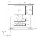
도 2는 본 발명의 일 실시예에 따른 표시장치(101)를 개략적으로 도시한 평면도이다. 도 3a는 도 2에 도시된 표시장치(101)의 배선에 대한 부분 평면도이고, 도 3b는 도 3a의 AR1 영역에 대한 평면도이다.2 is a plan view schematically showing a
도 2를 참조하면, 본 발명의 일 실시예에 의한 표시장치(101)는, 기판(111), 기판(111)상에 배치된 화소부(110), 주사 구동부(120), IC 실장 영역(130), 제1 테스트부(140) 및 패드부(180)를 포함한다.2, a
화소부(110)는 서로 교차하는 데이터 라인들(DL1 내지 DLm) 및 주사선들(SL1 내지 SLn)을 포함하며, 서로 다른 색의 빛을 방출하는 복수의 화소(P)들을 포함한다. 도 2를 참조하면, 데이터 라인들(DL1 내지 DLm)은 제1 방향으로 연장되고, 주사선들(SL1 내지 SLn)은 제2 방향으로 연장된다. 그러나, 데이터 라인들(DL1 내지 DLm)과 주사선들(SL1 내지 SLn)의 연장 방향이 이에 한정되는 것은 아니다.The
주사 구동부(120)는 외부로부터 공급되는 주사 구동전원 및 주사 제어 신호에 대응하여 주사 신호를 생성하고, 이를 주사선들(SL1 내지 SLn)로 순차적으로 공급한다.The
IC 실장 영역(130)은 화소부(110)의 데이터 라인들(DL1 내지 DLm)의 일 단에 연결된 다수의 데이터 패드(DP)들을 포함한다. 도시되지 않았지만 COG(chip on glass) 방식으로 데이터 패드(DP1 내지 DPm)들과 연결된 데이터 구동부가 IC 실장 영역(130)에 배치될 수 있다. 데이터 구동부(미도시)는 표시 데이터 및 데이터 제어 신호에 대응하여 데이터 신호를 생성하고, 이를 데이터 라인들(DL1 내지 DLm)로 공급한다.The
제1 테스트부(140)는 팬아웃부(190)에 배치된 링크선들(L1 내지 Lm)에 테스트 신호를 인가한다. 여기서, 링크선들(L1 내지 Lm)은 화소부(110)의 데이터 라인들(DL1 내지 DLm)로부터 IC 실장 영역(130)까지 연장된 선들이다. 링크선들(L1 내지 Lm)을 통해 데이터 라인들(DL1 내지 DLm)로 테스트 신호가 인가된다.The
제1 테스트부(140)는 팬아웃부(190)에 배치된 링크선들(L1 내지 Lm)과 데이터 라인들(DL1 내지 DLm)의 저항성 불량 및 쇼트 불량을 검출할 수 있다.The
저항성 불량 검출은 링크선들(L1 내지 Lm)의 크랙(crack)에 의한 저항 증가에 따라 화면에 발생하는 세로선 불량을 검출한다. 쇼트 불량 검출은 데이터 라인들(DL1 내지 DLm) 또는 링크선들(L1 내지 Lm)의 단락을 검출하는 것이다.The resistive failure detection detects a vertical line defect occurring on the screen in accordance with an increase in resistance due to a crack in the link lines L1 to Lm. The short defective detection is to detect a short of the data lines DL1 to DLm or the link lines L1 to Lm.
제1 테스트부(140)는 테스트 신호 및 테스트 제어 신호를 공급받고, 테스트 제어 신호에 대응하여 테스트 신호를 링크선들(L1 내지 Lm)을 경유하여 데이터 라인들(DL1 내지 DLm)로 공급한다.The
패드부(180)는 외부로부터 공급되는 전원들 및 신호들 중 적어도 하나를 전달하기 위한 다수의 패드(PD)들을 구비한다. 도 2에서 패드부(180)와 화소부(110) 의 각 구성부를 연결하는 라인의 위치와 수는 편의상 도시된 것으로, 다수의 라인들이 다른 위치에 배치될 수도 있다.The
제1 테스트부(140)는 IC 실장 영역(130)의 데이터 패드(DP)들과 테스트 신호선(14b) 사이에 배치된 스위칭 소자(TR)들을 포함한다. 스위칭 소자(TR)는 테스트 제어 신호(TEST_GATE)를 공급하는 테스트 제어선(14a) 및 테스트 신호(TEST_DATA)를 공급하는 테스트 신호선(14b)과 연결되고, 데이터 패드(DP)를 통해 데이터 라인(DL)과 연결된다.The
도 3b는 도 3a에 도시된 배선의 일부분인 AR1 영역에 대한 평면도이다.Fig. 3B is a plan view of the AR1 region, which is a part of the wiring shown in Fig. 3A.
본 발명의 일 실시예에 따르면, 스위칭 소자(TR)는 게이트 전극(GE), 제1 반도체층(SM1), 제2 반도체층(SM2), 소스 전극(SE) 및 드레인 전극(DE)을 포함한다.The switching element TR includes the gate electrode GE, the first semiconductor layer SM1, the second semiconductor layer SM2, the source electrode SE, and the drain electrode DE, according to an embodiment of the present invention. do.
구체적으로, 도 3a 및 3b를 참조하면, 스위칭 소자(TR)의 게이트 전극(GE)은 테스트 제어 신호(TEST_GATE)를 공급하는 테스트 제어선(14a)에 연결된다. 스위칭 소자(TR)의 소스 전극(SE)은 테스트 신호(TEST_DATA)를 공급하는 테스트 신호선(14b)에 연결되고, 드레인 전극(DE)은 데이터 패드(DP)에 연결된다. 하나의 데이터 패드(DP1)는 하나의 링크선(L1)을 통해 하나의 데이터 라인(DL1)과 연결된다. 그러나 본 발명의 일 실시예가 이러한 구조로 한정되는 것은 아니다. 제1 테스트부(140), IC 실장 영역(130), 데이터 패드(DP) 및 링크선들(L1 내지 Lm)은 다양한 형태로 이루어져 다양한 연결관계를 가질 수 있다. 한편, 스위칭 소자(TR)의 상세한 구조는 후술된다.Specifically, referring to FIGS. 3A and 3B, the gate electrode GE of the switching element TR is connected to a
예를 들어, 저항성 불량을 갖는 링크선과 연결된 데이터 라인(DL)에 연결된 화소(P)들은 주변 열(column)의 화소(p)들과 비교하여 휘도 차를 갖는다. 이를 근거로, 주변 열(column)에 비해 높거나 낮은 휘도로 발광하는 열(column)의 데이터 라인에 연결된 배선을 저항성 불량 또는 쇼트로 판단할 수 있다. 그리고, 주변 열(column)과의 휘도 차이 정도에 따라, 쇼트 불량과 저항성 불량을 구별할 수 있다.For example, pixels P connected to a data line DL connected to a link line having a resistance defect have a luminance difference in comparison with pixels p in a peripheral column. Based on this, a wiring connected to a data line of a column emitting light at a higher or lower luminance than a peripheral column can be judged as a resistance defect or a short circuit. Then, it is possible to distinguish between the short defect and the poor resistance depending on the degree of luminance difference from the peripheral column.
이하, 도 4a, 4b, 5a, 5b, 6a, 6b, 7a 및 7b를 참조하며, 도 3a 및 3b에 도시된 스위칭 소자(TR)들의 구체적인 실시예들(TR1, TR2, TR3, TR4)을 설명한다.Hereinafter, specific embodiments (TR1, TR2, TR3, TR4) of the switching elements TR shown in Figs. 3A and 3B will be described with reference to Figs. 4A, 4B, 5A, 5B, 6A, 6B, 7A and 7B do.
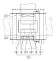
도 4a는 제1 테스트부(140)에 배치된 스위칭 소자(TR1)의 일 실시예에 대한 평면도이고, 도 4b는 도 4a의 A-A'를 따라 자른 단면도이다.4A is a plan view of an embodiment of the switching device TR1 disposed in the
도 3b, 도 4a 및 4b를 참조하면, 제1 테스트부(140)의 스위칭 소자(TR1)는 게이트 전극(GE), 제1 반도체층(SM1), 제2 반도체층(SM2), 소스 전극(SE) 및 드레인 전극(DE)을 포함하는 박막트랜지스터이다.3B, 4A, and 4B, the switching element TR1 of the
스위칭 소자(TR1)의 게이트 전극(GE)은 테스트 제어선(14a)과 연결된다.The gate electrode GE of the switching element TR1 is connected to the
제1 반도체층(SM1)과 제2 반도체층(SM2)은 게이트 전극(GE)과 적어도 일부 중첩되어 배치된다.The first semiconductor layer SM1 and the second semiconductor layer SM2 are disposed so as to overlap at least a part with the gate electrode GE.
소스 전극(SE)은 제1 반도체층(SM1) 및 제2 반도체층(SM2)과 연결되고, 또한 테스트 신호선(14b)과 연결된다. 소스 전극(SE)은 제1 반도체층(SM1) 및 제2 반도체층(SM2)과 적어도 일부 중첩된다.The source electrode SE is connected to the first semiconductor layer SM1 and the second semiconductor layer SM2 and is connected to the
드레인 전극(DE)은 소스 전극(SE)과 이격되어, 제1 반도체층(SM1) 및 제2 반도체층(SM2)과 연결되고, 또한 데이터 패드(DP)와 연결된다. 드레인 전극(DE)은 제1 반도체층(SM1) 및 제2 반도체층(SM2)과 적어도 일부 중첩된다.The drain electrode DE is spaced apart from the source electrode SE and connected to the first semiconductor layer SM1 and the second semiconductor layer SM2 and to the data pad DP. The drain electrode DE overlaps at least part of the first semiconductor layer SM1 and the second semiconductor layer SM2.
제1 반도체층(SM1)과 제2 반도체층(SM2)은 서로 이격되어 배치된다. 제1 반도체층(SM1)과 제2 반도체층(SM2)은 적어도 일부가 서로 중첩한다.The first semiconductor layer SM1 and the second semiconductor layer SM2 are disposed apart from each other. At least a part of the first semiconductor layer SM1 and the second semiconductor layer SM2 overlap each other.
도 4b를 참조하면, 제1 반도체층(SM1)과 제2 반도체층(SM2) 사이에 절연막(IL1, IL2)이 배치된다. 소스 전극(SE)과 드레인 전극(DE)은 각각 제2 반도체층(SM2)과 직접 접촉하고, 절연막(IL1, IL2)에 형성된 컨택홀(CH1, CH2)을 통하여 각각 제1 반도체층(SM1)과 연결된다.Referring to FIG. 4B, insulating films IL1 and IL2 are disposed between the first semiconductor layer SM1 and the second semiconductor layer SM2. The source electrode SE and the drain electrode DE directly contact the second semiconductor layer SM2 and are connected to the first semiconductor layer SM1 through the contact holes CH1 and CH2 formed in the insulating films IL1 and IL2, Lt; / RTI >
또한, 도 4b를 참조하면, 제1 반도체층(SM1)과 제2 반도체층(SM2) 사이에 게이트 전극(GE)이 배치된다. 보다 구체적으로, 제1 반도체층(SM1)과 게이트 전극(GE) 사이에 제1 절연막(IL1)이 배치되고, 게이트 전극(GE)과 제2 반도체층(SM2)과 사이에 제2 절연막(IL2)이 배치된다. 이 때, 제1 절연막(IL1)을 게이트 절연막이라 할 수 있다.Referring to FIG. 4B, a gate electrode GE is disposed between the first semiconductor layer SM1 and the second semiconductor layer SM2. More specifically, a first insulating film IL1 is disposed between the first semiconductor layer SM1 and the gate electrode GE, a second insulating film IL2 is provided between the gate electrode GE and the second semiconductor layer SM2, . At this time, the first insulating film IL1 may be referred to as a gate insulating film.
제1 반도체층(SM1) 및 제2 반도체층(SM2) 중 어느 하나는 산화물 반도체를 포함하고, 다른 하나는 실리콘계 반도체를 포함한다. 예를 들어, 제1 반도체층(SM1)이 실리콘계 반도체를 포함하고, 제2 반도체층(SM2)이 산화물 반도체를 포함할 수 있다. 반대로, 제1 반도체층(SM1)이 산화물 반도체를 포함하고, 제2 반도체층(SM2)이 실리콘계 반도체를 포함할 수도 있다.Any one of the first semiconductor layer SM1 and the second semiconductor layer SM2 includes an oxide semiconductor and the other includes a silicon-based semiconductor. For example, the first semiconductor layer SM1 may include a silicon-based semiconductor, and the second semiconductor layer SM2 may include an oxide semiconductor. Conversely, the first semiconductor layer SM1 may include an oxide semiconductor, and the second semiconductor layer SM2 may include a silicon-based semiconductor.
실리콘계 반도체는 결정질 실리콘을 포함할 수 있다. 예를 들어, 실리콘계 반도체로 저온 폴리실리콘(Low-temperature polycrystalline silicon, LTPS)이 사용될 수 있다. 실리콘계 반도체는 안정적인 전기적 특성을 갖는다.The silicon-based semiconductor may include crystalline silicon. For example, low-temperature polycrystalline silicon (LTPS) may be used as a silicon-based semiconductor. The silicon-based semiconductor has stable electrical characteristics.
산화물 반도체로, 아연(Zn), 인듐(In), 갈륨(Ga), 주석(Sn), 티타늄(Ti) 등의 산화물 및 이들의 합금 산화물이 있다. 예를 들어, 산화물 반도체는 산화 아연(ZnO), 아연-주석 산화물(ZTO), 아연-인듐 산화물(ZIO), 인듐 산화물(InO), 티타늄(TiO), 인듐-갈륨-아연 산화물(IGZO), 인듐-아연-주석 산화물(IZTO) 중 적어도 하나를 포함할 수 있다.As the oxide semiconductor, there are oxides such as zinc (Zn), indium (In), gallium (Ga), tin (Sn) and titanium (Ti), and alloy oxides thereof. For example, oxide semiconductors can be formed of a material selected from the group consisting of ZnO, ZTO, ZIO, InO, TiO, Indium-zinc-tin oxide (IZTO).
제1 반도체층(SM1) 또는 제2 반도체층(SM2) 형성을 위해 산화물 반도체에 불순물이 주입될 수 있다. 산화물 반도체 중 불순물이 선택적으로 주입된 부분은 소스 전극(SE) 및 드레인 전극(DE)과의 접촉부가 되고, 불순물이 주입되지 않은 부분은 채널 영역이 될 수 있다.Impurities may be implanted into the oxide semiconductor for the formation of the first semiconductor layer SM1 or the second semiconductor layer SM2. The portion of the oxide semiconductor in which the impurity is selectively implanted becomes a contact portion with the source electrode SE and the drain electrode DE, and the portion into which the impurity is not implanted can be a channel region.
산화물 반도체는 높은 전계 이동도, 낮은 문턱 전압, 낮은 누설 전류 등의 장점을 갖는다.The oxide semiconductor has advantages such as high electric field mobility, low threshold voltage, and low leakage current.
본 발명의 일 실시예에 따른 스위칭 소자(TR1)는 실리콘계 반도체의 특징과 산화물 반도체의 특징을 모두 가질 수 있어, 우수한 전기적 특성 및 높은 신호 전달 속도를 갖는다. 즉, 반도체층(SM1, SM2)이 좁은 폭을 가지더라도, 스위칭 소자(TR1)가 우수한 스위칭 특성을 갖는다. 따라서, 좁은 영역에 스위칭 소자(TR1)가 고밀도로 배치될 수 있다.The switching device TR1 according to an embodiment of the present invention can have both the characteristics of a silicon-based semiconductor and the characteristics of an oxide semiconductor, and has excellent electrical characteristics and a high signal transmission rate. That is, even if the semiconductor layers SM1 and SM2 have a narrow width, the switching element TR1 has excellent switching characteristics. Therefore, the switching element TR1 can be arranged at a high density in a narrow region.
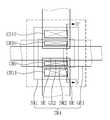
도 5a는 스위칭 소자(TR2)의 다른 일 실시예에 대한 평면도이고, 도 5b는 도 5a의 B-B'를 따라 자른 단면도이다.5A is a plan view of another embodiment of the switching device TR2, and FIG. 5B is a sectional view taken along line B-B 'of FIG. 5A.
도 5a 및 5b를 참조하면, 게이트 전극(GE)은 제1 게이트 전극(GE1) 및 제2 게이트 전극(GE2)을 포함한다. 여기서, 제1 게이트 전극(GE1) 및 제2 게이트 전극(GE2) 중 적어도 하나는 제1 반도체층(SM1)과 제2 반도체층(SM2) 사이에 배치될 수 있다.5A and 5B, the gate electrode GE includes a first gate electrode GE1 and a second gate electrode GE2. Here, at least one of the first gate electrode GE1 and the second gate electrode GE2 may be disposed between the first semiconductor layer SM1 and the second semiconductor layer SM2.
구체적으로, 기판(111) 상에 제1 게이트 전극(GE1)이 배치되고, 제1 게이트 전극(GE1) 상에 제1 절연막(IL1)이 배치되고, 제1 절연막(IL1) 상에 제1 반도체층(SM1)이 배치되고, 제1 반도체층(SM1) 상에 제2 절연막(IL2)이 배치되고, 제2 절연막(IL2) 상에 제2 게이트 전극(GE2)이 배치되고, 제2 게이트 전극(GE2) 상에 제3 절연막(IL3)이 배치되고, 제3 절연막(IL3) 상에 제2 반도체층(SM2)이 배치되고, 제2 반도체층(SM2) 상에 제2 반도체층(SM2)과 각각 접촉하는 소스 전극(SE)과 드레인 전극(DE)이 배치된다. 여기서, 소스 전극(SE)과 드레인 전극(DE)은 제2 절연막(IL2) 및 제3 절연막(IL3)을 관통하여 형성된 컨택홀(CH3, CH4)을 통하여 각각 제1 반도체층(SM1)과 연결된다.Specifically, the first gate electrode GE1 is disposed on the
도 6a는 스위칭 소자(TR3)의 또 다른 일 실시예에 대한 평면도이고, 도 6b는 도 6a의 C-C'를 따라 자른 단면도이다.FIG. 6A is a plan view of another embodiment of the switching device TR3, and FIG. 6B is a cross-sectional view taken along line C-C 'of FIG. 6A.
도 6a 및 6b를 참조하면, 게이트 전극(GE)은 제1 게이트 전극(GE1) 및 제2 게이트 전극을 포함하며, 제1 반도체층(SM1) 및 제2 반도체층(SM2)은 제1 게이트 전극(GE1)과 제2 게이트(GE2) 사이에 배치된다.6A and 6B, the gate electrode GE includes a first gate electrode GE1 and a second gate electrode. The first semiconductor layer SM1 and the second semiconductor layer SM2 are connected to the first gate electrode GE1, (GE1) and the second gate (GE2).
구체적으로, 기판(111) 상에 제1 게이트 전극(GE1)이 배치되고, 제1 게이트 전극(GE1) 상에 제1 절연막(IL1)이 배치되고, 제1 절연막(IL1) 상에 제1 반도체층(SM1)이 배치되고, 제1 반도체층(SM1) 상에 제2 절연막(IL2)이 배치되고, 제2 절연막(IL2) 상에 제2 반도체층(SM2)이 배치되고, 제2 반도체층(SM2)상에 제3 절연막(IL3)이 배치되고, 제3 절연막(IL3) 상에 제2 게이트 전극(GE2)이 배치되고, 제2 게이트 전극(GE2) 상에 제4 절연막(IL4)이 배치되고, 제4 절연막(IL4) 상에 소스 전극(SE)과 드레인 전극(DE)이 배치된다. 여기서, 소스 전극(SE)과 드레인 전극(DE)은 제4 절연막(IL4) 및 제3 절연막(IL3)을 관통하여 형성된 컨택홀(CH5, CH6)을 통하여 각각 제2 반도체층(SM2)과 연결되고, 제4 절연막(IL4), 제3 절연막(IL3) 및 제2 절연막(IL2)을 관통하여 형성된 컨택홀(CH7, CH8)을 통하여 각각 제1 반도체층(SM1)과 연결된다.Specifically, the first gate electrode GE1 is disposed on the
도 7a는 스위칭 소자(TR4)의 또 다른 일 실시예에 대한 평면도이고, 도 7b는 도 7a의 D-D'를 따라 자른 단면도이다.FIG. 7A is a plan view of another embodiment of the switching device TR4, and FIG. 7B is a sectional view taken along line D-D 'of FIG. 7A.
도 7a 및 7b를 참조하면, 기판(111) 상에 제1 반도체층(SM1)이 배치되고, 제1 반도체층(SM1) 상에 제1 절연막(IL1)이 배치되고, 제1 절연막(IL1) 상에 제1 게이트 전극(GE1)이 배치되고, 제1 게이트 전극(GE1) 상에 제2 절연막(IL2)이 배치되고, 제2 절연막(IL2) 상에 제2 반도체층(SM2)이 배치되고, 제2 반도체층(SM2)상에 제3 절연막(IL3)이 배치되고, 제3 절연막(IL3) 상에 제2 게이트 전극(GE2)이 배치되고, 제2 게이트 전극(GE2) 상에 제4 절연막(IL4)이 배치되고, 제4 절연막(IL4) 상에 소스 전극(SE)과 드레인 전극(DE)이 배치된다.7A and 7B, a first semiconductor layer SM1 is disposed on a
여기서, 소스 전극(SE)과 드레인 전극(DE)은 제4 절연막(IL4) 및 제3 절연막(IL3)을 관통하여 형성된 컨택홀(CH9, CH10)을 통하여 각각 제2 반도체층(SM2)과 연결되고, 제4 절연막(IL4), 제3 절연막(IL3), 제2 절연막(IL2) 및 제1 절연막(IL1)을 관통하여 형성된 컨택홀(CH11, CH12)을 통하여 각각 제1 반도체층(SM1)과 연결된다.The source electrode SE and the drain electrode DE are connected to the second semiconductor layer SM2 through the contact holes CH9 and CH10 formed through the fourth insulating film IL4 and the third insulating film IL3, And is electrically connected to the first semiconductor layer SM1 through the contact holes CH11 and CH12 formed through the fourth insulating film IL4, the third insulating film IL3, the second insulating film IL2, and the first insulating film IL1, Lt; / RTI >
도 8은 본 발명의 다른 일 실시예에 따른 표시장치(102)의 배선에 대한 부분 평면도이다.8 is a partial plan view of the wiring of the
도 8의 표시장치는(102)는 점등 테스트 및 링크선 테스트를 선택적으로 수행할 수 있는 제1 테스트부(140A)를 포함한다.The display device of FIG. 8 includes a
도 8을 참조하면, 화소부(110)는 서로 다른 색의 빛을 방출하는 제1화소들, 제2화소들 및 제3화소들을 포함한다. 제1화소 및 제2화소는 동일한 열(column)에 교대로 배열되고, 제3화소는 제1화소 및 제2화소가 배열된 열(column)의 인접한 열(column)에 일렬로 배치된다.Referring to FIG. 8, the
도 8에 따른 표시장치(102)에서, 제1화소는 적색의 빛을 방출하는 적색 화소(R)이고, 제2화소는 청색의 빛을 방출하는 청색 화소(B)이고, 제3화소는 녹색의 빛을 방출하는 녹색 화소(G)이다.8, the first pixel is a red pixel R that emits red light, the second pixel is a blue pixel B that emits blue light, and the third pixel is green (G) that emits light of a predetermined wavelength.
적색 화소(R)와 청색 화소(B)는 동일한 열에 교대로 배열되고, 녹색 화소(G)는 적색 화소(R)와 청색 화소(B)가 배열된 열의 인접한 열에 일렬로 배치된다.The red pixel R and the blue pixel B are alternately arranged in the same column and the green pixel G is arranged in a line in an adjacent column of the column in which the red pixel R and the blue pixel B are arranged.
이때, 적색 화소(R)와 청색 화소(B)는 녹색 화소(G)가 배열된 열을 중심으로, 적색 화소(R)들끼리, 그리고 청색 화소(B)들끼리 대각선 방향에 위치되어 체크보더 형태로 배열된다. 각 열에는 데이터 라인들(DL1 내지 DLm)이 배치된다.At this time, the red pixel R and the blue pixel B are located in the diagonal direction between the red pixels R and the blue pixels B, respectively, about the column in which the green pixels G are arranged, Lt; / RTI > In each column, data lines DL1 to DLm are arranged.
예를 들어, 제1 열에는 적색 화소(R)와 청색 화소(B)가 교대로 배열되고, 제2 열에는 녹색 화소(G)가 배열되고, 제3 열에는 제1 열과 반대 순서로 적색 화소(R)와 청색 화소(B)가 교대로 배열되고, 제4 열에는 녹색 화소(G)가 배열될 수 있다. 화소부(110)에는 제1 열 내지 제4 열이 반복적으로 배치될 수 있다.For example, the red pixel R and the blue pixel B are alternately arranged in the first column, the green pixel G is arranged in the second column, and the red pixel R is arranged in the third column in the opposite order to the first column. The red pixel R and the blue pixel B may be alternately arranged and the green pixel G may be arranged in the fourth column. The first to fourth columns may be repeatedly arranged in the
도 8에 따른 실시예에서 화소부(110)가 적색 화소(R), 청색 화소(B), 녹색 화소(G)를 포함하는 것을 설명하고 있으나, 화소부(110)는 적색, 녹색 및 청색 이외의 색을 표시하기 위한 화소(미도시)를 더 포함할 수도 있다.8, the
IC 실장 영역(130)에는 데이터 라인들(DL1 내지 DLm)로부터 연장된 링크선들(L1 내지 Lm)에 연결된 다수의 데이터 패드(DP)들이 배치된다.The
제1 테스트부(140A)는 스위칭 소자(TR)로 작동하는 다수의 테스트 스위치들(SW1 내지 SW8)을 포함한다. 여기서, 도 4a, 4b, 5a, 5b, 6a, 6b, 7a 및 7b에 도시된 스위칭 소자(TR1, TR2, TR3, TR4) 중 어느 하나가 각각의 테스트 스위치(SW1 내지 SW8)로 사용될 수 있다.The
각 테스트 스위치(SW1 내지 SW8)의 게이트 전극(GE)은 테스트 제어 신호를 공급하는 다수의 테스트 제어선들(141 내지 145) 중 하나에 연결되고, 소스 전극(SE)은 화소 테스트 신호 또는 링크선 테스트 신호를 공급하는 다수의 테스트 신호선들(146 내지 148) 중 하나와 연결될 수 있고, 드레인 전극(DE)은 데이터 패드(DP)를 통해 링크선들(L1 내지 Lm) 중 하나와 연결될 수 있다.The gate electrode GE of each of the test switches SW1 to SW8 is connected to one of a plurality of
구체적으로, 제1 테스트 스위치(SW1)의 게이트 전극(GE)은 제1 테스트 제어 신호(TEST_GATE_R)를 공급하는 제1 테스트 제어선(141)에 연결되고, 드레인 전극(DE)은 데이터 패드(DP)를 통해 제1 열의 데이터 라인(D1, D5, ...)에 연결되고, 소스 전극(SE)은 제1 테스트 신호(DC_R)를 공급하는 제1 테스트 신호선(146)에 연결된다. 제1 테스트 신호(DC_R)는 제1 화소 테스트 신호 또는 제1 링크선 테스트 신호일 수 있다.Specifically, the gate electrode GE of the first test switch SW1 is connected to the first
제2 테스트 스위치(SW2)의 게이트 전극(GE)은 제2 테스트 제어 신호(TEST_GATE_B)를 공급하는 제2 테스트 제어선(143)에 연결되고, 드레인 전극(DE)은 데이터 패드(DP)를 통해 제1 열의 데이터 라인(D1, D5, ...)에 연결되고, 소스 전극(SE)은 제2 테스트 신호(DC_B)를 공급하는 제2 테스트 신호선(148)에 연결된다. 제2 테스트 신호(DC_B)는 제2 화소 테스트 신호 또는 제2 링크선 테스트 신호일 수 있다.The gate electrode GE of the second test switch SW2 is connected to the second
제3 테스트 스위치(SW3)의 게이트 전극(GE)은 제3 테스트 제어 신호(TEST_GATE_G)를 공급하는 제3 테스트 제어선(142)에 연결되고, 드레인 전극(DE)은 데이터 패드(DP)를 통해 제2 열의 데이터 라인(D2, D6, ...)에 연결되고, 소스 전극(SE)은 제3 테스트 신호(DC_G)를 공급하는 제3 테스트 신호선(147)에 연결된다. 제3 테스트 신호(DC_G)는 제3 화소 테스트 신호 또는 제3 링크선 테스트 신호일 수 있다.The gate electrode GE of the third test switch SW3 is connected to the third
제4 테스트 스위치(SW4)의 게이트 전극(GE)은 제1 테스트 제어 신호(TEST_GATE_R)를 공급하는 제1 테스트 제어선(141)에 연결되고, 드레인 전극(DE)은 데이터 패드(DP)를 통해 제3 열의 데이터 라인(D3, D7, ...)에 연결되고, 소스 전극(SE)은 제2 테스트 신호(DC_B)를 공급하는 제2 테스트 신호선(148)에 연결된다.The gate electrode GE of the fourth test switch SW4 is connected to the first
제5 테스트 스위치(SW5)의 게이트 전극(GE)은 제2 테스트 제어 신호(TEST_GATE_B)를 공급하는 제2 테스트 제어선(143)에 연결되고, 드레인 전극(DE)은 데이터 패드(DP)를 통해 제3 열의 데이터 라인(D3, D7, ...)에 연결되고, 소스 전극(SE)은 제1 테스트 신호(DC_R)를 공급하는 제1 테스트 신호선(146)에 연결된다.The gate electrode GE of the fifth test switch SW5 is connected to the second
제6 테스트 스위치(SW6)의 게이트 전극(GE)은 제3 테스트 제어 신호(TEST_GATE_G)를 공급하는 제3 테스트 제어선(142)에 연결되고, 드레인 전극(DE)은 데이터 패드(DP)를 통해 제4 열의 데이터 라인(D4, D8, ...)에 연결되고, 소스 전극(SE)은 제7 테스트 스위치(SW7)의 드레인 전극(DE) 및 제 8 테스트 스위치(SW8)의 드레인 전극(DE)와 연결된다.The gate electrode GE of the sixth test switch SW6 is connected to the third
제7 테스트 스위치(SW7)의 게이트 전극(GE)은 제4 테스트 제어 신호(TEST_GATE_G1)를 공급하는 제4 테스트 제어선(144)에 연결되고, 드레인 전극(DE)은 제6 테스트 스위치(SW6)의 소스 전극(SE)에 연결되고, 소스 전극(SE)이 제3 테스트 신호(DC_G)를 공급하는 제3 테스트 신호선(147)에 연결된다. 제7 테스트 스위치(SW7)는 점등 테스트 동안 턴 온 상태이고, 링크선 테스트일 동안 턴 오프 상태이다.The gate electrode GE of the seventh test switch SW7 is connected to the fourth
제8 테스트 스위치(SW8)의 게이트 전극(GE)은 제5 테스트 제어 신호(TEST_GATE_G2)를 공급하는 제5 테스트 제어선(145)에 연결되고, 드레인 전극(DE)은 제6 테스트 스위치(SW6)의 소스 전극(SE)에 연결되고, 소스 전극(SE)은 제2 테스트 신호(DC_B)를 공급하는 제2 테스트 신호선(148)에 연결된다. 제8 테스트 스위치(SW8)는 점등 테스트 동안 턴 오프 상태이고, 링크선 테스트일 동안 턴 온 상태이다.The gate electrode GE of the eighth test switch SW8 is connected to the fifth
제7 테스트 스위치(SW7)와 제8 테스트 스위치(SW8)가 점등 테스트와 링크선 테스트에서 선택적으로 턴 온되어, 해당 테스트 신호를 인가할 수 있다.The seventh test switch SW7 and the eighth test switch SW8 are selectively turned on in the lighting test and the link test so that the corresponding test signal can be applied.
제1 내지 제5 테스트 제어선(141 내지 145)은 각각 점등 테스트 및 링크선 테스트가 진행되는 동안 패드부(180)로부터 게이트 온 레벨 또는 게이트 오프 레벨의 제어 신호(TEST_GATE_R, TEST_GATE_B, TEST_GATE_G, TEST_GATE_G1, TEST_GATE_G2)를 공급받고, 제1 내지 제8스위치(SW1 내지 SW8)의 턴 온 및 턴 오프를 제어한다.The first to fifth
제1 내지 제3 테스트 신호선(146 내지 148)은 패드부(180)로부터 점등 테스트가 진행되는 동안 제1 내지 제3 화소 테스트 신호를 공급받고, 링크선 테스트가 진행되는 동안 제1 내지 제3 링크선 테스트 신호를 공급받는다.The first to third
도 4a, 4b, 5a, 5b, 6a, 6b, 7a 및 7b에 도시된 스위칭 소자(TR1, TR2, TR3, TR4) 중 어느 하나가 각각의 테스트 스위치(SW1 내지 SW8)로 사용될 수 있기 때문에, 테스트 스위치(SW1 내지 SW8)는 산화물 반도체층과 실리콘계 반도체층을 포함한다. 이러한 테스트 스위치(SW1 내지 SW8)는 실리콘계 반도체의 특징과 산화물 반도체의 특징을 모두 가져 우수한 전기적 특성 및 높은 신호 전달 속도를 갖는다.Since any one of the switching elements TR1, TR2, TR3 and TR4 shown in Figs. 4A, 4B, 5A, 5B, 6A, 6B, 7A and 7B can be used as each of the test switches SW1 to SW8, The switches SW1 to SW8 include an oxide semiconductor layer and a silicon-based semiconductor layer. These test switches SW1 to SW8 have both characteristics of a silicon-based semiconductor and characteristics of an oxide semiconductor, and thus have excellent electrical characteristics and a high signal transmission rate.
따라서, 반도체층(SM1, SM2)가 좁은 폭을 가지더라도, 스위칭 소자가 우수한 스위칭 특성을 갖기 때문에, 스위칭 소자가 좁은 영역에 고밀도로 배치될 수 있다.Therefore, even if the semiconductor layers SM1 and SM2 have a narrow width, since the switching elements have excellent switching characteristics, the switching elements can be arranged at a high density in a narrow region.
도 9는 본 발명의 또 다른 일 실시예에 따른 표시장치(103)의 배선에 대한 부분 평면도이다.9 is a partial plan view of the wiring of the
도 9의 표시장치는(103)는 점등 테스트 및 링크선 테스트를 선택적으로 수행할 수 있는 제1 테스트부(140A)를 포함한다.The display device of FIG. 9 includes a
도 9의 화소부(110)는 서로 다른 색의 빛을 방출하는 제1화소들, 제2화소들 및 제3화소들을 포함한다. 제1화소 및 제2화소는 동일한 열(column)에 교대로 배열되고, 제3화소는 제1화소 및 제2화소가 배열된 열(column)의 인접한 열(column)에 일렬로 배치된다.The
도 9에 따른 표시장치(103)에서, 제1화소는 적색의 빛을 방출하는 적색 화소(R)이고, 제2화소는 녹색의 빛을 방출하는 녹색 화소(G)이고, 제3화소는 청색의 빛을 방출하는 청색 화소(B)이다. 적색 화소(R)와 녹색 화소(G)는 동일한 열에 교대로 배열되고, 청색 화소(B)는 적색 화소(R)와 녹색 화소(G)가 배열된 열의 인접한 열에 일렬로 배치된다.9, the first pixel is a red pixel R that emits red light, the second pixel is a green pixel G that emits green light, the third pixel is a blue pixel (B) that emits light of a blue color. The red pixel R and the green pixel G are alternately arranged in the same column and the blue pixel B is arranged in a line in an adjacent column of the column in which the red pixel R and the green pixel G are arranged.
이때, 적색 화소(R)와 녹색 화소(G)는 청색 화소(B)가 배열된 열을 중심으로, 적색 화소(R)들끼리, 그리고 녹색 화소(G)들끼리 대각선 방향에 위치되어 체크보더 형태로 배열된다. 각 열에는 데이터 라인들(DL1 내지 DLm)이 배치된다.At this time, the red pixel R and the green pixel G are located in the diagonal direction between the red pixels R and the green pixels G, with the row in which the blue pixels B are arranged as the center, Lt; / RTI > In each column, data lines DL1 to DLm are arranged.
예를 들어, 제1 열에는 적색 화소(R)와 녹색 화소(G)가 교대로 배열되고, 제2 열에는 청색 화소(B)가 배열되고, 제3 열에는 제1 열과 반대 순서로 적색 화소(R)와 녹색 화소(G)가 교대로 배열되고, 제4 열에는 청색 화소(B)가 배열될 수 있다. 화소부(110)에는 제1 열 내지 제4 열이 반복적으로 배치될 수 있다.For example, the red pixel R and the green pixel G are alternately arranged in the first column, the blue pixels B are arranged in the second column, and the red pixels R are arranged in the third column in the opposite order to the first column. The red pixel R and the green pixel G may be alternately arranged and the blue pixel B may be arranged in the fourth column. The first to fourth columns may be repeatedly arranged in the
도 9에 따른 실시예에서 화소부(110)가 적색 화소(R), 녹색 화소(G), 청색 화소(B)를 포함하는 것을 설명하고 있으나, 화소부(110)는 적색, 녹색 및 청색 이외의 색을 표시하기 위한 화소(미도시)를 더 포함할 수도 있다.9, the
IC 실장 영역(130)에는 데이터 라인들(DL1 내지 DLm)로부터 연장된 링크선들(L1 내지 Lm)에 연결된 다수의 데이터 패드(DP)들이 배치된다.The
제1 테스트부(140A)는 스위칭 소자(TR)로 작동하는 다수의 테스트 스위치들(SW1 내지 SW8)을 포함한다. 여기서, 도 4a, 4b, 5a, 5b, 6a, 6b, 7a 및 7b에 도시된 스위칭 소자(TR1, TR2, TR3, TR4) 중 어느 하나가 각각의 테스트 스위치(SW1 내지 SW8)로 사용될 수 있다.The
각 테스트 스위치(SW1 내지 SW8)의 게이트 전극(GE)은 테스트 제어 신호를 공급하는 다수의 테스트 제어선들(141 내지 145) 중 하나에 연결되고, 소스 전극(SE)은 화소 테스트 신호 또는 링크선 테스트 신호를 공급하는 다수의 테스트 신호선들(146 내지 148) 중 하나와 연결될 수 있고, 드레인 전극(DE)은 데이터 패드(DP)를 통해 링크선들(L1 내지 Lm) 중 하나와 연결될 수 있다.The gate electrode GE of each of the test switches SW1 to SW8 is connected to one of a plurality of
구체적으로, 제1 테스트 스위치(SW1)의 게이트 전극(GE)은 제1 테스트 제어 신호(TEST_GATE_R)를 공급하는 제1 테스트 제어선(141)에 연결되고, 드레인 전극(DE)은 데이터 패드(DP)를 통해 제1 열의 데이터 라인(D1, D5, ...)에 연결되고, 소스 전극(SE)은 제1 테스트 신호(DC_R)를 공급하는 제1 테스트 신호선(146)에 연결된다. 제1 테스트 신호(DC_R)는 제1 화소 테스트 신호 또는 제1 링크선 테스트 신호일 수 있다.Specifically, the gate electrode GE of the first test switch SW1 is connected to the first
제2 테스트 스위치(SW2)의 게이트 전극(GE)은 제2 테스트 제어 신호(TEST_GATE_G)를 공급하는 제2 테스트 제어선(143)에 연결되고, 드레인 전극(DE)은 데이터 패드(DP)를 통해 제1 열의 데이터 라인(D1, D5, ...)에 연결되고, 소스 전극(SE)은 제2 테스트 신호(DC_G)를 공급하는 제2 테스트 신호선(148)에 연결된다. 제2 테스트 신호(DC_G)는 제2 화소 테스트 신호 또는 제2 링크선 테스트 신호일 수 있다.The gate electrode GE of the second test switch SW2 is connected to the second
제3 테스트 스위치(SW3)의 게이트 전극(GE)은 제3 테스트 제어 신호(TEST_GATE_B)를 공급하는 제3 테스트 제어선(142)에 연결되고, 드레인 전극(DE)은 데이터 패드(DP)를 통해 제2 열의 데이터 라인(D2, D6, ...)에 연결되고, 소스 전극(SE)은 제3 테스트 신호(DC_B)를 공급하는 제3 테스트 신호선(147)에 연결된다. 제3 테스트 신호(DC_B)는 제3 화소 테스트 신호 또는 제3 링크선 테스트 신호일 수 있다.The gate electrode GE of the third test switch SW3 is connected to the third
제4 테스트 스위치(SW4)의 게이트 전극(GE)은 제1 테스트 제어 신호(TEST_GATE_R)를 공급하는 제1 테스트 제어선(141)에 연결되고, 드레인 전극(DE)은 데이터 패드(DP)를 통해 제3 열의 데이터 라인(D3, D7, ...)에 연결되고, 소스 전극(SE)은 제2 테스트 신호(DC_G)를 공급하는 제2 테스트 신호선(148)에 연결된다.The gate electrode GE of the fourth test switch SW4 is connected to the first
제5 테스트 스위치(SW5)의 게이트 전극(GE)은 제2 테스트 제어 신호(TEST_GATE_G)를 공급하는 제2 테스트 제어선(143)에 연결되고, 드레인 전극(DE)은 데이터 패드(DP)를 통해 제3 열의 데이터 라인(D3, D7, ...)에 연결되고, 소스 전극(SE)은 제1 테스트 신호(DC_R)를 공급하는 제1 테스트 신호선(146)에 연결된다.The gate electrode GE of the fifth test switch SW5 is connected to the second
제6 테스트 스위치(SW6)의 게이트 전극(GE)은 제3 테스트 제어 신호(TEST_GATE_B)를 공급하는 제3 테스트 제어선(142)에 연결되고, 드레인 전극(DE)은 데이터 패드(DP)를 통해 제4 열의 데이터 라인(D4, D8, ...)에 연결되고, 소스 전극(SE)은 제7 테스트 스위치(SW7)의 드레인 전극(DE) 및 제 8 테스트 스위치(SW8)의 드레인 전극(DE)와 연결된다.The gate electrode GE of the sixth test switch SW6 is connected to the third
제7 테스트 스위치(SW7)의 게이트 전극(GE)은 제4 테스트 제어 신호(TEST_GATE_B1)를 공급하는 제4 테스트 제어선(144)에 연결되고, 드레인 전극(DE)은 제6 테스트 스위치(SW6)의 소스 전극(SE)에 연결되고, 소스 전극(SE)이 제3 테스트 신호(DC_B)를 공급하는 제3 테스트 신호선(147)에 연결된다. 제7 테스트 스위치(SW7)는 점등 테스트 동안 턴 온 상태이고, 링크선 테스트일 동안 턴 오프 상태이다.The gate electrode GE of the seventh test switch SW7 is connected to the fourth
제8 테스트 스위치(SW8)의 게이트 전극(GE)은 제5 테스트 제어 신호(TEST_GATE_B2)를 공급하는 제5 테스트 제어선(145)에 연결되고, 드레인 전극(DE)은 제6 테스트 스위치(SW6)의 소스 전극(SE)에 연결되고, 소스 전극(SE)은 제2 테스트 신호(DC_G)를 공급하는 제2 테스트 신호선(148)에 연결된다. 제8 테스트 스위치(SW8)는 점등 테스트 동안 턴 오프 상태이고, 링크선 테스트일 동안 턴 온 상태이다.The gate electrode GE of the eighth test switch SW8 is connected to the fifth
제7 테스트 스위치(SW7)와 제8 테스트 스위치(SW8)가 점등 테스트와 링크선 테스트에서 선택적으로 턴 온되어, 해당 테스트 신호를 인가할 수 있다.The seventh test switch SW7 and the eighth test switch SW8 are selectively turned on in the lighting test and the link test so that the corresponding test signal can be applied.
제1 내지 제5 테스트 제어선(141 내지 145)은 각각 점등 테스트 및 링크선 테스트가 진행되는 동안 패드부(180)로부터 게이트 온 레벨 또는 게이트 오프 레벨의 제어 신호(TEST_GATE_R, TEST_GATE_G, TEST_GATE_B, TEST_GATE_B1, TEST_GATE_B2)를 공급받고, 제1 내지 제8스위치(SW1 내지 SW8)의 턴 온 및 턴 오프를 제어한다.The first to fifth
제1 내지 제3 테스트 신호선(146 내지 148)은 패드부(180)로부터 점등 테스트가 진행되는 동안 제1 내지 제3 화소 테스트 신호를 공급받고, 링크선 테스트가 진행되는 동안 제1 내지 제3 링크선 테스트 신호를 공급받는다.The first to third
도 4a, 4b, 5a, 5b, 6a, 6b, 7a 및 7b에 도시된 스위칭 소자(TR1, TR2, TR3, TR4) 중 어느 하나가 각각의 테스트 스위치(SW1 내지 SW8)로 사용될 수 있기 때문에, 테스트 스위치(SW1 내지 SW8)는 산화물 반도체층과 실리콘계 반도체층을 포함한다. 이러한 테스트 스위치(SW1 내지 SW8)는 실리콘계 반도체의 특징과 산화물 반도체의 특징을 모두 가져 우수한 전기적 특성 및 높은 신호 전달 속도를 갖는다.Since any one of the switching elements TR1, TR2, TR3 and TR4 shown in Figs. 4A, 4B, 5A, 5B, 6A, 6B, 7A and 7B can be used as each of the test switches SW1 to SW8, The switches SW1 to SW8 include an oxide semiconductor layer and a silicon-based semiconductor layer. These test switches SW1 to SW8 have both characteristics of a silicon-based semiconductor and characteristics of an oxide semiconductor, and thus have excellent electrical characteristics and a high signal transmission rate.
따라서, 반도체층(SM1, SM2)가 좁은 폭을 가지더라도, 스위칭 소자가 우수한 스위칭 특성을 갖기 때문에, 스위칭 소자가 좁은 영역에 고밀도로 배치될 수 있다.Therefore, even if the semiconductor layers SM1 and SM2 have a narrow width, since the switching elements have excellent switching characteristics, the switching elements can be arranged at a high density in a narrow region.
도 10은 본 발명의 또 다른 일 실시예에 따른 표시장치(104)를 개략적으로 도시한 평면도이고, 도 11은 도 10에 도시된 표시장치(104)의 배선에 대한 부분 평면도이다.FIG. 10 is a plan view schematically showing a
도 10 및 11에 따른 표시장치(104)는 도 2에 도시된 표시장치(101)와 비교하여, 제2 테스트부(150)를 더 포함한다.The
도 11을 참조하면, 기판(111) 상에 배치된 화소부(110)는 적색 화소(R), 녹색 화소(G) 및 청색 화소(B)를 포함한다. 설명의 편의를 위해, 도 11에서 복수의 주사선(SL1 내지 SLn)은 생략되었다. 도 11에 따른 표시장치(103)의 제2 테스트부(150)는 배선 테스트의 초기화 및 점등 테스트를 수행할 수 있다.11, a
IC 실장 영역(130)에는 데이터 라인들(DL1 내지 DLm) 각각의 일 단에서 연장된 링크선들(L1 내지 Lm)과 연결된 데이터 패드들(DP1 내지 DPm)이 배치된다.The
제2 테스트부(150)는 데이터 라인들(DL1 내지 DLm) 각각의 타단에 연결된 제1 초기화 스위치(SB11)들, 제2 초기화 스위치(SB12)들 및 제3 초기화 스위치(SB13)들을 포함할 수 있다. 도 4a, 4b, 5a, 5b, 6a, 6b, 7a 및 7b에 도시된 스위칭 소자(TR1, TR2, TR3, TR4) 중 어느 하나가 각각의 초기화 스위치들(SB11, SB12, SB13)로 사용될 수 있다. 즉, 초기화 스위치들(SB11, SB12, SB13)은 산화물 반도체층과 실리콘계 반도체층을 포함한다. 이러한 초기화 스위치들(SB11, SB12, SB13)은 실리콘계 반도체의 특징과 산화물 반도체의 특징을 모두 가져 우수한 전기적 특성 및 높은 신호 전달 속도를 갖는다.The
제1 내지 제3 초기화 스위치들(SB11, SB12, SB13)의 게이트 전극(GE)은 초기화 테스트 제어 신호(DC_GATE)를 공급하는 테스트 제어선(16a)에 연결된다. 제1 초기화 스위치(SB11)의 소스 전극(SE)은 제1 초기화 테스트 신호(DC_R)를 공급하는 제1 테스트 신호선(16b)에 연결되고, 드레인 전극(DE)은 적색 화소(R)가 배열된 열의 데이터 라인에 연결된다. 제2 초기화 스위치(SB12)의 소스 전극(SE)은 제2 초기화 테스트 신호(DC_G)를 공급하는 제2 테스트 신호선(16c)에 연결되고, 드레인 전극(DE)은 녹색 화소(G)가 배열된 열의 데이터 라인에 연결된다. 제3 초기화 스위치(SB13)의 소스 전극(SE)은 제3 초기화 테스트 신호(DC_B)를 공급하는 제3 테스트 신호선(16d)에 연결되고, 드레인 전극(DE)은 청색 화소(B)가 배열된 열의 데이터 라인에 연결된다.The gate electrodes GE of the first to third initialization switches SB11, SB12 and SB13 are connected to a
제1 테스트부(140)는 IC 실장 영역(130)의 데이터 패드(DP)들과 테스트 신호선(14b) 사이에 배치된 제2 스위치(SB2)들을 포함할 수 있다. 제2 스위치(SB2)의 게이트 전극(GE)은 테스트 제어 신호(TEST_GATE)를 공급하는 테스트 제어선(14a)에 연결된다. 제2 스위치(SB2)의 소스 전극(SE)은 테스트 신호(TEST_DATA)를 공급하는 테스트 신호선(14b)에 연결되고, 드레인 전극(DE)은 데이터 패드(DP1 내지 DPm)들 중 하나에 연결된다.The
제2 스위치(SB2)로 도 4a, 4b, 5a, 5b, 6a, 6b, 7a 및 7b에 도시된 스위칭 소자(TR1, TR2, TR3, TR4) 중 어느 하나가 사용될 수 있다. 즉, 제2 스위치(SB2)는 산화물 반도체층과 실리콘계 반도체층을 포함한다. 이러한 제2 스위치(SB2)는 실리콘계 반도체의 특징과 산화물 반도체의 특징을 모두 가져 우수한 전기적 특성 및 높은 신호 전달 속도를 갖는다.Any one of the switching elements TR1, TR2, TR3 and TR4 shown in Figs. 4A, 4B, 5A, 5B, 6A, 6B, 7A and 7B can be used as the second switch SB2. That is, the second switch SB2 includes an oxide semiconductor layer and a silicon-based semiconductor layer. The second switch SB2 has both characteristics of a silicon semiconductor and characteristics of an oxide semiconductor, and has excellent electrical characteristics and a high signal transmission rate.
도 12는 본 발명의 또 다른 일 실시예에 따른 유기발광 표시장치(105)의 화소에 대한 평면도이고, 도 13은 도 12의 절단선 I-I'와 II-II'를 따라 자른 단면도 및 스위칭 소자(TR)의 단면도이다.12 is a plan view of a pixel of an OLED display according to another embodiment of the present invention, FIG. 13 is a cross-sectional view taken along the line I-I 'and II-II' Sectional view of the device TR.
본 발명의 또 다른 일 실시예에 따른 유기발광 표시장치(105)는 기판(211), 배선부(230) 및 유기 발광 소자(310)를 포함한다.The organic light emitting
기판(211)은 유리, 석영, 세라믹, 및 플라스틱 등으로 이루어진 군에서 선택된 절연성 재료로 만들어질 수 있다. 또한, 기판(211)으로 고분자 필름이 사용될 수도 있다.The
기판(211) 상에 버퍼층(220)이 배치된다. 버퍼층(220)은 다양한 무기막들 및 유기막들 중에서 선택된 하나 이상의 막을 포함할 수 있다. 버퍼층(220)은 생략될 수도 있다.A
배선부(230)는 버퍼층(220) 상에 배치된다. 배선부(230)는 복수의 박막트랜지스터들(10, 20)을 포함하며, 유기 발광 소자(310)를 구동한다. 즉, 유기 발광 소자(310)는 배선부(230)로부터 전달받은 구동 신호에 따라 빛을 방출하여 화상을 표시한다.The
배선부(230)와 동일층에 테스트부의 스위칭 소자(TR)가 배치된다(도 13 참조). 도 4a, 4b, 5a, 5b, 6a, 6b, 7a 및 7b에 도시된 스위칭 소자(TR1, TR2, TR3, TR4) 중 어느 하나가 스위칭 소자(TR)로 사용될 수 있다. 도 13을 참조하면, 스위칭 소자(TR)는 도 4a 및 4b에 도시된 스위칭 소자(TR1)와 동일한 적층 구조를 갖는다. 이하, 중복을 피하기 위해 스위칭 소자(TR)에 대한 상세한 설명은 생략된다.The switching element TR of the test section is disposed on the same layer as the wiring section 230 (see Fig. 13). Any one of the switching elements TR1, TR2, TR3 and TR4 shown in Figs. 4A, 4B, 5A, 5B, 6A, 6B, 7A and 7B can be used as the switching element TR. Referring to FIG. 13, the switching element TR has the same stacking structure as the switching element TR1 shown in FIGS. 4A and 4B. Hereinafter, a detailed description of the switching element TR is omitted in order to avoid redundancy.
도 12 및 13에, 하나의 화소에 두 개의 박막트랜지스터(TFT)(10, 20)와 하나의 축전 소자(capacitor)(80)가 구비된 2Tr-1Cap 구조의 능동 구동(active matrix, AM)형 유기발광 표시장치가 도시되어 있다. 그러나, 본 실시예가 이러한 구조로 한정되는 것은 아니다. 예컨대, 유기발광 표시장치(105)는 하나의 화소에 셋 이상의 박막트랜지스터와 둘 이상의 축전 소자를 포함할 수 있으며, 별도의 배선을 더 포함할 수 있다. 여기서, 화소는 화상을 표시하는 최소 단위를 말하며, 유기발광 표시장치(104)는 복수의 화소들을 통해 화상을 표시한다.12 and 13 show an active matrix (AM) type TFT having a 2Tr-1Cap structure in which two thin film transistors (TFTs) 10 and 20 and one
하나의 화소는 스위칭 박막트랜지스터(10), 구동 박막트랜지스터(20), 축전 소자(80), 및 유기 발광 소자(organic light emitting diode, OLED)(310)를 포함한다. 또한, 일 방향을 따라 연장되는 게이트 라인(251)과, 게이트 라인(251)과 절연 교차되는 데이터 라인(271) 및 공통 전원 라인(272)도 배선부(230)에 배치된다. 하나의 화소(PX)는 게이트 라인(251), 데이터 라인(271) 및 공통 전원 라인(272)을 경계로 정의될 수 있으나, 반드시 이에 한정되는 것은 아니다. 화소정의막 또는 블랙 매트릭스에 의하여 화소(PX)가 정의될 수도 있다.One pixel includes a switching
축전 소자(80)는 층간 절연막(260)을 사이에 두고 배치된 한 쌍의 축전판(258, 278)을 포함한다. 여기서, 층간 절연막(260)은 유전체가 된다. 축전 소자(80)에서 축전된 전하와 양 축전판(258, 278) 사이의 전압에 의해 축전용량이 결정된다.The
스위칭 박막트랜지스터(10)는 스위칭 반도체층(231), 스위칭 게이트 전극(252), 스위칭 소스 전극(273), 및 스위칭 드레인 전극(274)을 포함한다. 구동 박막트랜지스터(20)는 구동 반도체층(232), 구동 게이트 전극(255), 구동 소스 전극(276), 및 구동 드레인 전극(277)을 포함한다. 반도체층(231, 232)과 게이트 전극(252, 255)은 게이트 절연막(240)에 의하여 절연된다.The switching
스위칭 박막트랜지스터(10)는 발광시키고자 하는 화소(PX)를 선택하는 스위칭 소자로 사용된다. 스위칭 게이트 전극(252)은 게이트 라인(251)에 연결된다. 스위칭 소스 전극(273)은 데이터 라인(271)에 연결된다. 스위칭 드레인 전극(274)은 스위칭 소스 전극(273)으로부터 이격 배치되며 어느 한 축전판(258)과 연결된다.The switching
구동 박막트랜지스터(20)는 선택된 화소(PX) 내의 유기 발광 소자(310)의 발광층(312)을 발광시키기 위한 구동 전원을 화소 전극(PE)인 제1 전극(311)에 인가한다. 구동 게이트 전극(255)은 스위칭 드레인 전극(274)과 연결된 축전판(258)과 연결된다. 구동 소스 전극(276) 및 다른 한 축전판(278)은 각각 공통 전원 라인(272)과 연결된다. 구동 드레인 전극(277)은 평탄화막(265)에 구비된 컨택홀(contact hole)을 통해 유기 발광 소자(310)의 제1 전극(311)과 연결된다.The driving
이와 같은 구조에 의하여, 스위칭 박막트랜지스터(10)는 게이트 라인(251)에 인가되는 게이트 전압에 의해 작동되어 데이터 라인(271)에 인가되는 데이터 전압을 구동 박막트랜지스터(20)로 전달하는 역할을 한다. 공통 전원 라인(272)으로부터 구동 박막트랜지스터(20)에 인가되는 공통 전압과 스위칭 박막트랜지스터(10)로부터 전달된 데이터 전압의 차에 해당하는 전압이 축전 소자(80)에 저장되고, 축전 소자(80)에 저장된 전압에 대응하는 전류가 구동 박막트랜지스터(20)를 통해 유기 발광 소자(310)로 흘러 유기 발광 소자(310)가 발광한다.The switching
도 13을 참조하면, 구동 박막트랜지스터(20)의 구동 소스 전극(276) 및 구동 드레인 전극(277)은 테스트부에 배치된 스위칭 소자(TR)의 소스전극(SE) 및 드레인(DE) 전극과 동일층에 배치된다. 구동 소스 전극(276) 및 구동 드레인 전극(277)은 스위칭 소자(TR)의 소스전극(SE) 및 드레인(DE) 전극과 동일한 재료로 동일한 공정에 의해 만들어질 수 있다.13, the driving
또한, 도 13을 참조하면, 스위칭 박막트랜지스터(10)의 스위칭 소스 전극(273) 및 스위칭 드레인 전극(274) 역시, 테스트부 배치된 스위칭 소자(TR)의 소스전극(SE) 및 드레인(DE) 전극과 동일층에 배치된다. 스위칭 소스 전극(273) 및 스위칭 드레인 전극(274) 역시 스위칭 소자(TR)의 소스 전극(SE) 및 드레인(DE) 전극과 동일한 재료로 동일한 공정에 의해 만들어질 수 있다.13, the switching
도 13을 참조하면, 구동 게이트 전극(255)과 스위칭 게이트 전극(252)은 스위칭 소자(TR)의 게이트 전극(GE)과 동일층에 배치된다. 구동 게이트 전극(255) 과 스위칭 게이트 전극(252)은 스위칭 소자(TR)의 게이트 전극(GE)과 동일한 재료로 이루어진다.Referring to FIG. 13, the driving
또한, 구동 반도체층(232)과 스위칭 반도체층(231)은 스위칭 소자(TR)의 제1 반도체층(SM1) 및 제2 반도체층(SM2) 중 어느 하나와 동일층에 배치될 수 있다.The driving
도 13를 참조하면, 구동 반도체층(232)과 스위칭 반도체층(231)은 스위칭 소자(TR)의 제1 반도체층(SM1)과 동일층에 배치된다. 이 때, 구동 반도체층(232)과 스위칭 반도체층(231)은 스위칭 소자(TR)의 제1 반도체층(SM1)과 동일한 재료로 동일한 공정에 의해 만들어질 수 있다.Referring to FIG. 13, the driving
예를 들어, 구동 반도체층(232), 스위칭 반도체층(231) 및 스위칭 소자(TR)의 제1 반도체층(SM1)은 산화물 반도체를 포함할 수 있다. 이 때, 스위칭 소자(TR)의 제2 반도체층(SM2)은 실리콘계 반도체를 포함할 수 있다. 실리콘계 반도체로 저온 폴리실리콘(Low-temperature polycrystalline silicon, LTPS)이 사용될 수 있다.For example, the first semiconductor layer SM1 of the driving
그러나, 본 발명의 일 실시예가 이에 한정되는 것은 아니다. 구동 반도체층(232)과 스위칭 반도체층(231)은 스위칭 소자(TR)의 제2 반도체층(SM2)과 동일한 재료로 동일한 공정에 의해 만들어질 수도 있다.However, the embodiment of the present invention is not limited thereto. The driving
유기 발광 소자(310)는 제1 전극(311), 제1 전극(311) 상에 배치된 발광층(312), 및 발광층(312) 상에 배치된 제2 전극(313)을 포함한다. 발광층(312)은 저분자 유기물 또는 고분자 유기물로 이루어진다. 제1 전극(311) 및 제2 전극(313)으로부터 각각 정공과 전자가 발광층(312) 내부로 주입되고, 이와 같이 주입된 정공과 전자가 결합되어 형성된 엑시톤(exiton)이 여기상태로부터 기저상태로 떨어질 때 발광이 이루어진다.The organic
도 13을 참조하면, 제1 전극(311)은 양극이다. 제1 전극(311)은 광투과성을 갖는 투광성 전극일 수도 있으며, 광반사성을 갖는 반사 전극일 수도 있다.Referring to FIG. 13, the
제2 전극(313)은 반투과막으로 형성될 수도 있고, 반사막으로 형성될 수도 있다.The
제1 전극(311)과 발광층(312) 사이에 정공 주입층(hole injection layer; HIL) 및 정공 수송층(hole transporting layer; HTL) 중 적어도 하나가 더 배치될 수 있으며, 발광층(312)과 제2 전극(313) 사이에 전자 수송층(electron transporting layer; ETL) 및 전자 주입층(electron injection layer; EIL) 중 적어도 하나가 더 배치될 수 있다. 발광층(312), 정공 주입층(HIL), 정공 수송층(HTL), 전자 수송층(ETL) 및 전자 주입층(EIL)은 유기 물질로 만들어질 수 있기 때문에, 이들을 유기층이라고도 한다.At least one of a hole injection layer (HIL) and a hole transporting layer (HTL) may be further disposed between the
화소 정의막(290)은 개구부를 갖는다. 화소 정의막(290)의 개구부는 제1 전극(311)의 일부를 드러낸다. 화소 정의막(290)의 개구부에서 제1 전극(311) 상에 발광층(312) 및 제2 전극(313)이 차례로 적층된다. 여기서, 상기 제2 전극(313)은 발광층(312) 뿐만 아니라 화소 정의막(290) 위에도 형성된다. 한편, 정공 주입층, 정공 수송층, 전자 수송층 및 전자 주입층은 화소 정의막(290)과 제2 전극(313) 사이에도 배치될 수 있다. 유기 발광 소자(310)는 화소 정의막(290)의 개구부 내에 위치한 발광층(312)에서 빛을 발생시킨다. 이와 같이, 화소 정의막(290)은 발광 영역을 정의할 수도 있다.The
외부 환경으로부터 유기 발광 소자(310)를 보호하기 위해 제2 전극(313)상에 캡핑층(미도시)이 배치될 수도 있다.A capping layer (not shown) may be disposed on the
도 13을 참조하면, 제2 전극(313)상에 박막 봉지층(350)이 배치된다.Referring to FIG. 13, a thin-
박막 봉지층(350)은 하나 이상의 무기막(351, 353) 및 하나 이상의 유기막(352)을 포함하며, 수분이나 산소와 같은 외기가 유기발광소자(310)로 침투하는 것을 방지한다.The thin
박막 봉지층(350)은 무기막(351, 353)과 유기막(352)이 교호적으로 적층된 구조를 갖는다. 도 12에서 박막 봉지층(350)은 2개의 무기막(351, 353)과 1개의 유기막(352)을 포함하고 있으나, 박막 봉지층(350)의 구조가 이에 한정되는 것은 아니다.The thin
무기막(351, 353)은 Al2O3, TiO2, ZrO, SiO2, AlON, AlN, SiON, Si3N4, ZnO, 및 Ta2O5 중 하나 이상의 무기물을 포함한다. 무기막(351, 353)은 화학증착(chemical vapor deposition, CVD)법 또는 원자층 증착(atomic layer depostion, ALD)법을 통해 형성된다. 무기막(351, 353)은 해당 기술 분야의 종사자에게 공지된 다양한 방법을 통해 형성될 수 있다.The
유기막(352)은 고분자(polymer) 계열의 소재로 만들어진다. 여기서, 고분자 계열의 소재는 아크릴계 수지, 에폭시계 수지, 폴리이미드, 및 폴리에틸렌 등을 포함한다. 또한, 유기막(352)은 열증착 공정을 통해 형성된다. 유기막(352)을 형성하기 위한 열증착 공정은 유기 발광 소자(310)를 손상시키지 않는 온도 범위 내에서 진행된다. 유기막(352)은 해당 기술 분야의 종사자에게 공지된 다양한 방법을 통해 형성될 수 있다.The
박막의 밀도가 치밀하게 형성된 무기막(351, 353)이 주로 수분 또는 산소의 침투를 억제한다. 대부분의 수분 및 산소는 무기막(351, 353)에 의해 유기 발광 소자(310)로의 침투가 차단된다.The
무기막(351, 353)을 통과한 수분 및 산소는 유기막(352)에 의해 다시 차단된다. 유기막(352)은 무기막(351, 353)에 비해 상대적으로 투습 방지 효과는 적다. 하지만, 유기막(352)은 투습 억제 외에 무기막(351, 353)과 무기막(351, 353) 사이에서 각층들 간의 응력을 줄여주는 완충층의 역할도 함께 수행한다. 또한, 유기막(352)은 평탄화 특성을 가지므로, 박막 봉지층(350)의 최상부면이 평탄해질 수 있다.The moisture and oxygen that have passed through the
박막 봉지층(350)은 10㎛ 이하의 얇은 두께를 가질 수 있다. 따라서, 유기발광 표시장치(104) 역시 얇은 두께를 가질 수 있다. 이와 같이 박막 봉지층(350)이 적용됨으로써, 유기발광 표시장치(104)가 플렉서블 특성을 가질 수 있다.The thin
도시되지 않았지만, 제2 전극(313) 상에 박막 봉지층(350) 대신 봉기 기판이 배치될 수도 있다.Although not shown, a protruding substrate may be disposed on the
도 14는 본 발명의 또 다른 일 실시예에 따른 유기발광 표시장치(106)의 화소 및 스위칭 소자에 대한 단면도이다.14 is a cross-sectional view of a pixel and a switching element of an organic
도 14에 도시된 유기발광 표시장치(106)는, 도 13에 도시된 유기발광 표시장치(105)와 비교하여, 서로 다른 구조를 갖는 스위칭 박막트랜지스터(10)와 구동 박막트랜지스터(20)를 포함한다.14 includes the switching
도 14를 참조하면, 구동 소스 전극(276), 구동 드레인 전극(277), 스위칭 소스 전극(273) 및 스위칭 드레인 전극(274)은 스위칭 소자(TR)의 소스전극(SE) 및 드레인(DE) 전극과 동일층에 배치된다. 이들은 동일한 재료를 이용하는 동일 공정에 의해 만들어질 수 있다.14, the driving
스위칭 게이트 전극(252), 구동 게이트 전극(255) 및 스위칭 소자(TR)의 게이트 전극(GE)은 동일층에 배치된다. 구동 게이트 전극(255), 스위칭 게이트 전극(252) 및 스위칭 소자(TR)의 게이트 전극(GE)은 동일한 재료를 이용하는 동일 공정에 의해 만들어질 수 있다.The switching
도 14를 참조하면, 구동 박막트랜지스터(20)의 구동 반도체층(232)은 스위칭 소자(TR)의 제1 반도체층(SM1)과 동일층에 배치된다. 이들은 동일한 재료를 이용하는 동일 공정에 의해 만들어질 수 있다.Referring to FIG. 14, the driving
또한, 스위칭 박막트랜지스터(10)의 스위칭 반도체층(231)은 스위칭 소자(TR)의 제2 반도체층(SM2)과 동일층에 배치된다. 이들은 동일한 재료를 이용하는 동일 공정에 의해 만들어질 수 있다.The switching
예를 들어, 구동 반도체층(232)과 제1 반도체층(SM1)은 산화물 반도체를 포함하고, 스위칭 반도체층(231)과 제2 반도체층(SM2)은 실리콘계 반도체를 포함할 수 있다. 반대로, 구동 반도체층(232)과 제1 반도체층(SM1)은 실리콘계 반도체를 포함하고, 스위칭 반도체층(231)과 제2 반도체층(SM2)은 산화물 반도체를 포함할 수 있다. 실리콘계 반도체로 저온 폴리실리콘(Low-temperature polycrystalline silicon, LTPS)이 사용될 수 있다.For example, the driving
그러나, 본 발명의 일 실시예가 이에 한정되는 것은 아니다. 구동 반도체층(232)은 스위칭 소자(TR)의 제2 반도체층(SM2)과 동일층에 배치되고, 스위칭 반도체층(231)은 스위칭 소자(TR)의 제1 반도체층(SM1)과 동일층에 배치될 수도 있다.However, the embodiment of the present invention is not limited thereto. The driving
도 15는 본 발명의 또 다른 일 실시예에 따른 액정 표시장치(107)의 화소에 대한 평면도이고, 도 16은 도 15의 절단선 III-III'를 따라 자른 단면도 및 스위칭 소자(TR)의 단면도이다.FIG. 15 is a plan view of a pixel of a liquid
도 15의 액정 표시장치(107)는, 도 16에 도시된 바와 같이 표시 기판(410), 대향기판(420) 및 액정층(LC)을 포함한다.15 includes a
표시기판(410)은, 기판(401) 및 기판(401) 상에 배치된 제1 절연막(411), 게이트 라인(GL), 데이터 라인(DL), 박막트랜지스터(TFT), 게이트 절연막(421), 층간 절연막(431), 컬러 필터(451, 452), 평탄화막(491) 및 화소 전극(PE)을 포함한다.The
기판(401) 상에 스위칭 소자(TR)의 제1 반도체층(SM1)이 배치되고, 그 위에 제1 절연막(411)이 배치된다.The first semiconductor layer SM1 of the switching element TR is disposed on the
제1 절연막(411) 상에 게이트 라인(GL) 및 게이트 라인(GL)으로부터 연장된 게이트 전극(441)이 배치된다. 게이트 라인(GL)과 게이트 전극(441)은 동일층에 배치된다.A gate electrode GL extending from the gate line GL and a
게이트 라인(GL) 및 게이트 전극(441)은 알루미늄(Al)이나 알루미늄 합금과 같은 알루미늄 계열의 금속, 은(Ag)이나 은 합금과 같은 은 계열의 금속, 구리(Cu)나 구리 합금과 같은 구리 계열의 금속, 또는 몰리브덴(Mo)이나 몰리브덴 합금과 같은 몰리브덴 계열의 금속으로 만들어질 수 있다. 이와 달리, 게이트 라인(GL) 및 게이트 전극(GE)은 크롬(Cr), 탄탈륨(Ta) 및 티타늄(Ti) 중 어느 하나로 만들어질 수 있다. 또한, 게이트 라인(GL) 및 게이트 전극(GE)은 물리적 성질이 다른 적어도 두 개의 도전막을 포함하는 다중막 구조를 가질 수도 있다.The gate line GL and the
게이트 절연막(421)은 게이트 라인(GL) 및 게이트 전극(441) 상에 배치된다. 이때, 게이트 절연막(421)은 게이트 라인(GL) 및 게이트 전극(441)을 포함한 기판(401)의 전면(全面)에 배치될 수 있다. 게이트 절연막(421)은 질화 규소(SiNx) 또는 산화 규소(SiOx) 등으로 만들어질 수 있다. 게이트 절연막(421)은 물리적 성질이 다른 적어도 두 개의 절연막들을 포함하는 다중막 구조를 가질 수 있다.The
반도체층(442)은 게이트 절연막(421) 상에 배치된다. 반도체층(442)은 게이트 전극(441), 소스 전극(443) 및 드레인 전극(444)과 중첩한다. 반도체층(442)은 비정질 규소 또는 다결정 규소 등으로 만들어질 수 있다. 반도체층(442)은 산화물 반도체 재료를 포함할 수도 있다. 반도체층(442) 상에 저항성 접촉층(미도시)이 배치될 수도 있다.The
데이터 라인(DL)은 게이트 절연막(421) 상에 위치하며, 게이트 라인(GL)과 교차한다.The data line DL is located on the
소스 전극(443)은 반도체층(442)과 일부 중첩하여 배치된다. 소스 전극(443)은 데이터 라인(DL)으로부터 연장된다. 예를 들어, 도 13에 도시된 바와 같이, 소스 전극(443)은 데이터 라인(DL)으로부터 게이트 전극(441)을 향해 돌출된 형태를 갖는다.The
소스 전극(443)은 몰리브덴, 크롬, 탄탈륨 및 티타늄 등 내화성 금속(refractory metal) 또는 이들의 합금으로 만들어질 수 있으며, 내화성 금속막과 저저항 도전막을 포함하는 다중막 구조를 가질 수 있다. 다중막 구조의 예로, 크롬 또는 몰리브덴(또는 몰리브덴 합금) 하부막과 알루미늄 (또는 알루미늄 합금) 상부막으로 된 이중막, 몰리브덴 (또는 몰리브덴 합금) 하부막과 알루미늄 (또는 알루미늄 합금) 중간막과 몰리브덴 (또는 몰리브덴 합금) 상부막으로 된 삼중막 등이 있다. 소스 전극(SE)은 이외에도 여러 가지 다양한 금속 또는 도전체로 만들어질 수 있다.The
드레인 전극(444)은 소스 전극(443)과 이격되어 반도체층(442)과 일부 중첩하여 배치된다. 드레인 전극(444)은 화소 전극(PE)에 연결된다. 드레인 전극(444)은 소스 전극(443)과 동일한 공정으로 동시에 만들어질 수 있다.The
게이트 전극(441), 반도체층(442), 소스 전극(443) 및 드레인 전극(444)에 의해 박막트랜지스터(TFT)가 이루어진다.A thin film transistor TFT is formed by the
박막트랜지스터(TFT)의 채널(channel) 영역은 소스 전극(443)과 드레인 전극(DE) 사이의 반도체층(442) 부분에 위치한다.A channel region of the thin film transistor TFT is located in a portion of the
액정 표시장치(105)의 박막트랜지스터(TFT)와 함께 테스트부의 스위칭 소자(TR)가 배치된다. 도 4a, 4b, 5a, 5b, 6a, 6b, 7a 및 7b에 도시된 스위칭 소자(TR1, TR2, TR3, TR4) 중 어느 하나가 스위칭 소자(TR)로 사용될 수 있다. 도 16를 참조하면, 스위칭 소자(TR)는 도 4a 및 4b에 도시된 스위칭 소자(TR1)와 동일한 적층 구조를 갖는다.The switching element TR of the test section is disposed together with the thin film transistor TFT of the liquid
도 16을 참조하면, 박막트랜지스터(TFT)의 소스 전극(443) 및 드레인 전극(444)은 테스트부에 배치된 스위칭 소자(TR1)의 소스 전극(SE) 및 드레인 전극(DE)과 동일층에 배치된다. 또한, 박막트랜지스터(TFT)의 소스 전극(443) 및 드레인 전극(444)은 스위칭 소자(TR1)의 소스 전극(SE) 및 드레인 전극(DE)과 동일한 재료로 동일한 공정에 의해 만들어질 수 있다.16, the
도 16을 참조하면, 박막트랜지스터(TFT)의 게이트 전극(441)은 스위칭 소자(TR1)의 게이트 전극(GE)과 동일층에 배치된다. 박막트랜지스터(TFT)의 게이트 전극(441)은 스위칭 소자(TR)의 게이트 전극(GE)과 동일한 재료로 동일한 공정에 의해 만들어질 수 있다.Referring to FIG. 16, the
또한, 박막트랜지스터(TFT)의 반도체층(442)은 스위칭 소자(TR1)의 제1 반도체층(SM1) 및 제2 반도체층(SM2) 중 어느 하나와 동일층에 배치될 수 있다. 도 16을 참조하면, 박막트랜지스터(TFT)의 반도체층(442)은 스위칭 소자(TR1)의 제2 반도체층(SM2)과 동일층에 배치된다. 이 때, 박막트랜지스터(TFT)의 반도체층(442)은 스위칭 소자(TR1)의 제2 반도체층(SM2)과 동일한 재료로 동일한 공정에 의해 만들어질 수 있다.The
층간 절연막(431)은 데이터 라인(DL), 소스 전극(443), 드레인 전극(444) 및 게이트 절연막(421) 상에 배치된다. 이때, 층간 절연막(431)은 데이터 라인(DL), 소스 전극(443), 드레인 전극(444) 및 게이트 절연막(421)을 포함한 기판(401)의 전면(全面)에 배치될 수 있다. 도 15 및 16을 참조하면, 층간 절연막(431)은 드레인 콘택홀(432)을 갖는다. 드레인 콘택홀(432)에 의해 드레인 전극(DE)이 노출된다.The
층간 절연막(431)은 질화 규소(SiNx) 또는 산화 규소(SiOx)와 같은 무기 절연물로 만들어질 수 있으며, 유기막으로 만들어질 수도 있다. 또한 층간 절연막(431)은 하부 무기막과 상부 유기막을 포함하는 이중막 구조를 가질 수도 있다.The
제1 컬러 필터(451) 및 제2 컬러 필터(452)는 층간 절연막(431) 상에 배치된다. 제1 및 제2 컬러 필터(451, 452)의 가장자리는 게이트 라인(GL), 박막트랜지스터(TFT) 및 데이터 라인(DL) 상에 위치할 수 있다. 인접한 제1 및 제2 컬러 필터(451, 452)의 가장자리는 서로 중첩할 수 있다. 각각의 컬러 필터(451, 452)는 드레인 전극(444) 상에 위치하는 개구부를 갖는다.The
제1 컬러 필터(451)와 제2 컬러 필터(452)는 서로 다른 컬러를 가지며, 각각 적색 컬러 필터, 녹색 컬러 필터, 청색 컬러 필터, 원청색(cyan) 컬러 필터, 원적색(magenta) 컬러 필터, 황색(yellow) 컬러 필터 및 백색(white) 컬러 필터 중 어느 하나일 수 있다.The
도 15 및 16에 도시되지 않았지만, 액정 표시장치(105)는 제3 컬러 필터를 더 포함할 수 있다. 제3 컬러 필터는 제1 컬러 필터(451) 및 제2 컬러 필터(452)와 다른 컬러를 가지며, 적색, 녹색, 청색, 원청색(cyan), 원적색(magenta) 및 황색(yellow) 중 어느 하나의 컬러를 가질 수 있다.Although not shown in Figs. 15 and 16, the liquid
컬러필터(451, 452)는 밀봉 기판(402) 상에 배치될 수도 있다.The color filters 451 and 452 may be disposed on the sealing substrate 402.
평탄화막(491)은 컬러 필터(451, 452) 상에 배치된다. 이때, 평탄화막(491)은 컬러 필터(451, 452) 및 층간 절연막(431)을 포함한 기판(401)의 전면(全面)에 배치될 수 있다. 평탄화막(491)은 드레인 콘택홀(432)에 대응되게 위치한 개구부를 가질 수 있다.The
평탄화막(491)은 보호막 기능을 하며, 화소 전극(PE)의 하부를 평탄화하는 역할을 한다. 평탄화막(491)을 보호막이라고도 한다. 평탄화막(491)은 유기물로 만들어질 수 있는데, 예를 들어, 감광성 유기물 또는 감광성 수지 조성물로 만들어질 수 있다. 이 경우, 평탄화막(491)을 유기막이라고도 한다.The
화소 전극(PE)은 드레인 콘택홀(432)을 통해 드레인 전극(444)에 연결된다. 화소 전극(PE)은 평탄화막(491) 상에 배치된다. 화소 전극(PE)의 가장자리 일부는 차광부(476)와 중첩할 수 있다.The pixel electrode PE is connected to the
차광부(476)는 화소 전극(PE) 및 평탄화막(491) 상에 배치된다. 예를 들어, 차광부(476)는 박막트랜지스터(TFT), 게이트 라인들(GL) 및 데이터 라인(DL)과 중첩 배치되어, 빛샘을 차단한다.The light-shielding
차광부(476) 상에 컬럼 스페이서(472)가 위치할 수 있다. 컬럼 스페이서(472)는 대향기판(420)을 향해 차광부(476)로부터 소정 높이로 돌출된 형상을 갖는다. 컬럼 스페이서(472)는 표시기판(410)과 대향기판(420) 간의 셀갭(cell gap)을 유지시킨다.The
컬럼 스페이서(472)는 차광부(476)와 일체로 구성될 수 있다. 이 경우, 컬럼 스페이서(472)와 차광부(476)는 동일한 물질로 동시에 제조될 수 있다. 이러한 컬럼 스페이서(472)와 차광부(476)를 블랙 컬럼 스페이서(BCS)라고도 한다.The
대향기판(420)은 밀봉 기판(402) 및 밀봉 기판(402) 상에 배치된 공통 전극(CE)을 포함한다.The
화소전극(PE) 상에 액정층(LC)이 배치된다. 즉, 액정층(LC)은 기판(401)과 밀봉 기판(402) 사이에 배치된다. 보다 구체적으로, 표시기판(410)과 대향기판(420)에 의해 정의된 공간에 액정층(LC)이 위치할 수 있다.A liquid crystal layer LC is disposed on the pixel electrode PE. That is, the liquid crystal layer LC is disposed between the
또한, 표시기판(410), 액정층(LC) 및 대향기판(420)을 포함하는 패널을 액정 표시패널(400)이라고도 한다.The panel including the
이상에서 설명된 표시장치의 실시예는 예시적인 것에 불과하며, 본 발명의 보호범위는 본 발명 기술분야의 통상의 지식을 가진 자라면 이로부터 다양한 변형 및 균등예를 포함할 수 있다.The embodiments of the display device described above are merely illustrative, and the scope of protection of the present invention may include various modifications and equivalents to those skilled in the art.
110: 화소부120: 주사 구동부
130: IC 실장 영역140: 제1 테스트부
180: 패드부190: 팬아웃부
14a: 테스트 제어선14b: 테스트 신호선
L1 내지 Lm: 링크선DP: 데이터 패드110: pixel portion 120: scan driver
130: IC mounting region 140:
180: Pad part 190: Fan out part
14a:
L1 to Lm: link line DP: data pad
Claims (23)
Translated fromKorean상기 기판 상에 배치되며, 데이터 라인과 연결된 화소를 포함하는 화소부;
상기 데이터 라인의 일단에 연결된 데이터 패드; 및
테스트 제어 신호를 공급하는 테스트 제어선, 테스트 신호를 공급하는 테스트 신호선 및 상기 데이터 패드와 연결된 스위칭 소자를 포함하는 제1 테스트부;를 포함하며,
상기 스위칭 소자는,
상기 테스트 제어선과 연결된 게이트 전극;
상기 게이트 전극과 중첩되어 배치된 제1 반도체층 및 제2 반도체층;
상기 제1 반도체층 및 상기 제2 반도체층과 연결되고, 상기 테스트 신호선과 연결된 소스 전극; 및
상기 소스 전극과 이격되어 상기 제1 반도체층 및 상기 제2 반도체층과 연결되고, 상기 데이터 패드와 연결된 드레인 전극;을 포함하며,
상기 제1 반도체층 및 제2 반도체층 중 어느 하나는 산화물 반도체를 포함하고, 다른 하나는 실리콘계 반도체를 포함하는 표시장치.Board;
A pixel portion disposed on the substrate, the pixel portion including a pixel connected to a data line;
A data pad coupled to one end of the data line; And
And a first test section including a test control line for supplying a test control signal, a test signal line for supplying a test signal, and a switching element connected to the data pad,
The switching device includes:
A gate electrode connected to the test control line;
A first semiconductor layer and a second semiconductor layer overlapping with the gate electrode;
A source electrode connected to the first semiconductor layer and the second semiconductor layer and connected to the test signal line; And
And a drain electrode spaced apart from the source electrode and connected to the first semiconductor layer and the second semiconductor layer and connected to the data pad,
Wherein one of the first semiconductor layer and the second semiconductor layer includes an oxide semiconductor and the other includes a silicon semiconductor.
상기 유기발광소자와 연결된 박막트랜지스터를 더 포함하며,
상기 박막트랜지스터는 게이트 전극, 반도체층, 소스전극 및 드레인 전극을 포함하며,
상기 박막트랜지스터의 소스전극 및 드레인 전극은 상기 스위칭 소자의 소스전극 및 드레인 전극과 동일층에 배치된 표시장치.17. The method of claim 16,
And a thin film transistor connected to the organic light emitting device,
Wherein the thin film transistor includes a gate electrode, a semiconductor layer, a source electrode, and a drain electrode,
Wherein the source electrode and the drain electrode of the thin film transistor are arranged in the same layer as the source electrode and the drain electrode of the switching element.
상기 화소전극과 연결된 박막트랜지스터를 더 포함하며,
상기 박막트랜지스터는 게이트 전극, 반도체층, 소스전극 및 드레인 전극을 포함하며,
싱기 박막트랜지스터의 소스전극 및 드레인 전극은 상기 스위칭 소자의 소스전극 및 드레인 전극과 동일층에 배치된 표시장치.21. The method of claim 20,
And a thin film transistor connected to the pixel electrode,
Wherein the thin film transistor includes a gate electrode, a semiconductor layer, a source electrode, and a drain electrode,
And the source electrode and the drain electrode of the thin film transistor are arranged in the same layer as the source electrode and the drain electrode of the switching element.
Priority Applications (5)
| Application Number | Priority Date | Filing Date | Title |
|---|---|---|---|
| KR1020160117272AKR102716282B1 (en) | 2016-09-12 | 2016-09-12 | Display device having test unit |
| US15/693,567US10847432B2 (en) | 2016-09-12 | 2017-09-01 | Display device including a test unit |
| EP17190682.9AEP3293764B1 (en) | 2016-09-12 | 2017-09-12 | Display device including a test unit |
| CN201710816988.2ACN107818968B (en) | 2016-09-12 | 2017-09-12 | Display device including test unit |
| US17/101,189US11557520B2 (en) | 2016-09-12 | 2020-11-23 | Display device including a test unit |
Applications Claiming Priority (1)
| Application Number | Priority Date | Filing Date | Title |
|---|---|---|---|
| KR1020160117272AKR102716282B1 (en) | 2016-09-12 | 2016-09-12 | Display device having test unit |
Publications (2)
| Publication Number | Publication Date |
|---|---|
| KR20180030286Atrue KR20180030286A (en) | 2018-03-22 |
| KR102716282B1 KR102716282B1 (en) | 2024-10-11 |
Family
ID=59887038
Family Applications (1)
| Application Number | Title | Priority Date | Filing Date |
|---|---|---|---|
| KR1020160117272AActiveKR102716282B1 (en) | 2016-09-12 | 2016-09-12 | Display device having test unit |
Country Status (4)
| Country | Link |
|---|---|
| US (2) | US10847432B2 (en) |
| EP (1) | EP3293764B1 (en) |
| KR (1) | KR102716282B1 (en) |
| CN (1) | CN107818968B (en) |
Cited By (3)
| Publication number | Priority date | Publication date | Assignee | Title |
|---|---|---|---|---|
| KR20210033108A (en)* | 2019-09-17 | 2021-03-26 | 삼성디스플레이 주식회사 | Display device |
| KR20210157704A (en)* | 2020-06-22 | 2021-12-29 | 엘지디스플레이 주식회사 | Thin film transistor array substrate and display device |
| US12217640B2 (en) | 2021-04-27 | 2025-02-04 | Samsung Display Co., Ltd. | Display panel, electronic device including the same, and method of fabricating electronic device |
Families Citing this family (30)
| Publication number | Priority date | Publication date | Assignee | Title |
|---|---|---|---|---|
| KR102716282B1 (en)* | 2016-09-12 | 2024-10-11 | 삼성디스플레이 주식회사 | Display device having test unit |
| KR102512925B1 (en) | 2016-11-23 | 2023-03-21 | 가부시키가이샤 한도오따이 에네루기 켄큐쇼 | Display devices, display modules, and electronic devices |
| CN106876334B (en)* | 2017-03-10 | 2019-11-29 | 京东方科技集团股份有限公司 | The manufacturing method and array substrate of array substrate |
| WO2018179121A1 (en)* | 2017-03-29 | 2018-10-04 | シャープ株式会社 | Semiconductor device and method for manufacturing semiconductor device |
| KR20200039867A (en)* | 2018-10-05 | 2020-04-17 | 삼성디스플레이 주식회사 | Organic light emitting diode display device |
| US10910413B2 (en)* | 2018-10-10 | 2021-02-02 | HKC Corporation Limited | Method of manufacturing array substrate and array substrate |
| US11903299B2 (en)* | 2018-11-16 | 2024-02-13 | Sharp Kabushiki Kaisha | Display device |
| JP2020119809A (en)* | 2019-01-25 | 2020-08-06 | 株式会社ジャパンディスプレイ | Display device, manufacturing method thereof, and multi-panel display panel |
| KR102724173B1 (en)* | 2019-04-11 | 2024-10-31 | 삼성디스플레이 주식회사 | Display device and method of testing the same |
| CN110649045B (en)* | 2019-10-31 | 2022-08-26 | 京东方科技集团股份有限公司 | Organic light emitting display panel and display device |
| EP4057266A4 (en)* | 2019-11-08 | 2022-10-19 | BOE Technology Group Co., Ltd. | Array substrate and display device |
| KR102780550B1 (en)* | 2019-11-20 | 2025-03-12 | 삼성디스플레이 주식회사 | Display device and inspection method of the display device |
| CN111128063B (en)* | 2020-01-20 | 2021-03-23 | 云谷(固安)科技有限公司 | Display panel test circuit and method and display panel |
| KR102651587B1 (en)* | 2020-01-22 | 2024-03-27 | 삼성디스플레이 주식회사 | Inspecting apparatus for display panel and display apparatus having the same |
| KR102667016B1 (en)* | 2020-03-10 | 2024-05-21 | 삼성디스플레이 주식회사 | Display panel test circuit |
| CN113410149B (en)* | 2020-03-16 | 2025-08-29 | 三星显示有限公司 | Display device |
| CN113466252B (en)* | 2020-03-30 | 2024-07-30 | 昆山国显光电有限公司 | Display panel, detection method of display panel and display device |
| CN111508369B (en) | 2020-05-19 | 2022-07-15 | 云谷(固安)科技有限公司 | Display panel and display device |
| CN111798795A (en)* | 2020-06-30 | 2020-10-20 | 云谷(固安)科技有限公司 | Display device |
| CN114667504B (en)* | 2020-10-22 | 2025-09-05 | 京东方科技集团股份有限公司 | Display substrate and manufacturing method thereof, and display device |
| CN112420538B (en)* | 2020-11-10 | 2023-06-02 | 武汉华星光电半导体显示技术有限公司 | An array substrate, testing method and display device |
| CN113013254A (en)* | 2021-02-26 | 2021-06-22 | 合肥维信诺科技有限公司 | Thin film transistor, preparation method thereof and display panel |
| JP2022135619A (en)* | 2021-03-05 | 2022-09-15 | シャープディスプレイテクノロジー株式会社 | Active matrix substrate and manufacturing method thereof |
| CN113314546B (en)* | 2021-05-21 | 2023-06-02 | 深圳市华星光电半导体显示技术有限公司 | Array substrate, array substrate testing method and display panel |
| GB202114437D0 (en)* | 2021-10-08 | 2021-11-24 | Graphcore Ltd | Method of testing a stacked integrated circuit device |
| CN115019703B (en)* | 2021-11-30 | 2023-05-09 | 荣耀终端有限公司 | Display panel, detection method and electronic device |
| TWI850686B (en)* | 2022-06-27 | 2024-08-01 | 住華科技股份有限公司 | Test device, forming method and testing method thereof |
| KR20240022005A (en)* | 2022-08-10 | 2024-02-20 | 삼성디스플레이 주식회사 | Display panel |
| CN115548078B (en)* | 2022-09-30 | 2025-03-28 | 京东方科技集团股份有限公司 | Display panel and display device |
| CN116360168B (en)* | 2023-05-11 | 2023-08-18 | 惠科股份有限公司 | display device |
Citations (5)
| Publication number | Priority date | Publication date | Assignee | Title |
|---|---|---|---|---|
| US8803206B1 (en)* | 2012-12-29 | 2014-08-12 | Monolithic 3D Inc. | 3D semiconductor device and structure |
| US20140291669A1 (en)* | 2013-03-29 | 2014-10-02 | Lg Display Co., Ltd. | Thin-Film Transistor, Method for Manufacturing the Same and Display Device Comprising the Same |
| US20160079285A1 (en)* | 2014-09-12 | 2016-03-17 | Chunghwa Picture Tubes, Ltd. | Double thin film transistor and method of manufacturing the same |
| US20160163870A1 (en)* | 2014-12-08 | 2016-06-09 | Semiconductor Energy Laboratory Co., Ltd. | Semiconductor Device, Manufacturing Method of Semiconductor Device, and Electronic Device |
| US20160247934A1 (en)* | 2013-05-09 | 2016-08-25 | Semiconductor Energy Laboratory Co., Ltd. | Semiconductor Device and Manufacturing Method Thereof |
Family Cites Families (15)
| Publication number | Priority date | Publication date | Assignee | Title |
|---|---|---|---|---|
| TWI333094B (en)* | 2005-02-25 | 2010-11-11 | Au Optronics Corp | System and method for display testing |
| KR101100426B1 (en)* | 2005-05-10 | 2011-12-30 | 삼성전자주식회사 | A semiconductor device comprising a single crystal silicon layer, a semiconductor device including the same, and a flat panel display device and a method of manufacturing the semiconductor device |
| KR20080049216A (en)* | 2006-11-30 | 2008-06-04 | 엘지디스플레이 주식회사 | Liquid Crystal Display and Inspection Method |
| JP4374552B2 (en)* | 2007-04-12 | 2009-12-02 | ソニー株式会社 | Substrate manufacturing method, substrate manufacturing system, and display device manufacturing method |
| US8049253B2 (en)* | 2007-07-11 | 2011-11-01 | Semiconductor Energy Laboratory Co., Ltd. | Semiconductor device and method for manufacturing the same |
| KR101101070B1 (en) | 2009-10-12 | 2011-12-30 | 삼성모바일디스플레이주식회사 | Organic light emitting display |
| WO2011055625A1 (en) | 2009-11-06 | 2011-05-12 | Semiconductor Energy Laboratory Co., Ltd. | Semiconductor device and operating method thereof |
| KR20180030255A (en)* | 2009-11-30 | 2018-03-21 | 가부시키가이샤 한도오따이 에네루기 켄큐쇼 | Liquid crystal display device, method for driving the same, and electronic device including the same |
| WO2011125353A1 (en) | 2010-04-07 | 2011-10-13 | シャープ株式会社 | Circuit board, display device, and method for manufacturing circuit board |
| TW201338102A (en)* | 2012-03-14 | 2013-09-16 | Wintek Corp | Active component and active device array substrate |
| KR20150089252A (en)* | 2014-01-27 | 2015-08-05 | 삼성디스플레이 주식회사 | Display substrate and method of manufacturing mother substrate for display substrate |
| US9595546B2 (en) | 2014-02-25 | 2017-03-14 | Lg Display Co., Ltd. | Display backplane and method of fabricating the same |
| KR102237834B1 (en) | 2014-10-31 | 2021-04-12 | 엘지디스플레이 주식회사 | Thin Film Transistor Substrate Including Metal Oxide Semiconductor having Capping Layer |
| CN104992960B (en)* | 2015-06-08 | 2018-01-30 | 京东方科技集团股份有限公司 | A kind of display panel and its manufacture method, TFT method of testings |
| KR102716282B1 (en)* | 2016-09-12 | 2024-10-11 | 삼성디스플레이 주식회사 | Display device having test unit |
- 2016
- 2016-09-12KRKR1020160117272Apatent/KR102716282B1/enactiveActive
- 2017
- 2017-09-01USUS15/693,567patent/US10847432B2/enactiveActive
- 2017-09-12EPEP17190682.9Apatent/EP3293764B1/enactiveActive
- 2017-09-12CNCN201710816988.2Apatent/CN107818968B/enactiveActive
- 2020
- 2020-11-23USUS17/101,189patent/US11557520B2/enactiveActive
Patent Citations (5)
| Publication number | Priority date | Publication date | Assignee | Title |
|---|---|---|---|---|
| US8803206B1 (en)* | 2012-12-29 | 2014-08-12 | Monolithic 3D Inc. | 3D semiconductor device and structure |
| US20140291669A1 (en)* | 2013-03-29 | 2014-10-02 | Lg Display Co., Ltd. | Thin-Film Transistor, Method for Manufacturing the Same and Display Device Comprising the Same |
| US20160247934A1 (en)* | 2013-05-09 | 2016-08-25 | Semiconductor Energy Laboratory Co., Ltd. | Semiconductor Device and Manufacturing Method Thereof |
| US20160079285A1 (en)* | 2014-09-12 | 2016-03-17 | Chunghwa Picture Tubes, Ltd. | Double thin film transistor and method of manufacturing the same |
| US20160163870A1 (en)* | 2014-12-08 | 2016-06-09 | Semiconductor Energy Laboratory Co., Ltd. | Semiconductor Device, Manufacturing Method of Semiconductor Device, and Electronic Device |
Cited By (4)
| Publication number | Priority date | Publication date | Assignee | Title |
|---|---|---|---|---|
| KR20210033108A (en)* | 2019-09-17 | 2021-03-26 | 삼성디스플레이 주식회사 | Display device |
| KR20210157704A (en)* | 2020-06-22 | 2021-12-29 | 엘지디스플레이 주식회사 | Thin film transistor array substrate and display device |
| KR20240127939A (en)* | 2020-06-22 | 2024-08-23 | 엘지디스플레이 주식회사 | Thin film transistor array substrate and display device |
| US12217640B2 (en) | 2021-04-27 | 2025-02-04 | Samsung Display Co., Ltd. | Display panel, electronic device including the same, and method of fabricating electronic device |
Also Published As
| Publication number | Publication date |
|---|---|
| EP3293764B1 (en) | 2019-08-07 |
| US20210074597A1 (en) | 2021-03-11 |
| US11557520B2 (en) | 2023-01-17 |
| EP3293764A1 (en) | 2018-03-14 |
| US20180076102A1 (en) | 2018-03-15 |
| CN107818968A (en) | 2018-03-20 |
| KR102716282B1 (en) | 2024-10-11 |
| CN107818968B (en) | 2023-01-24 |
| US10847432B2 (en) | 2020-11-24 |
Similar Documents
| Publication | Publication Date | Title |
|---|---|---|
| KR102716282B1 (en) | Display device having test unit | |
| KR102801694B1 (en) | Organic light emitting display apparatus and method of manufacturing thereof | |
| US11437444B2 (en) | Display device | |
| KR102565936B1 (en) | Display device | |
| US10157973B2 (en) | Organic light emitting display device | |
| US10026793B2 (en) | Organic light emitting diode display | |
| US11621401B2 (en) | Display device | |
| KR20250050821A (en) | Display Device | |
| EP3748678B1 (en) | Display device | |
| US11574972B2 (en) | Display apparatus including a thin-film transistor including a silicon semiconductor and a thin-film transistor including an oxide semiconductor | |
| KR20160137872A (en) | Organic light emitting diode display and manufacturing method thereof | |
| KR102315889B1 (en) | Display panel | |
| US9614157B2 (en) | Organic light emitting diode display having a plurality of data drivers and manufacturing method thereof | |
| KR101960390B1 (en) | Display device having a thin film transistor |
Legal Events
| Date | Code | Title | Description |
|---|---|---|---|
| PA0109 | Patent application | Patent event code:PA01091R01D Comment text:Patent Application Patent event date:20160912 | |
| PG1501 | Laying open of application | ||
| A201 | Request for examination | ||
| PA0201 | Request for examination | Patent event code:PA02012R01D Patent event date:20210907 Comment text:Request for Examination of Application Patent event code:PA02011R01I Patent event date:20160912 Comment text:Patent Application | |
| E902 | Notification of reason for refusal | ||
| PE0902 | Notice of grounds for rejection | Comment text:Notification of reason for refusal Patent event date:20231116 Patent event code:PE09021S01D | |
| E701 | Decision to grant or registration of patent right | ||
| PE0701 | Decision of registration | Patent event code:PE07011S01D Comment text:Decision to Grant Registration Patent event date:20240708 | |
| GRNT | Written decision to grant | ||
| PR0701 | Registration of establishment | Comment text:Registration of Establishment Patent event date:20241007 Patent event code:PR07011E01D | |
| PR1002 | Payment of registration fee | Payment date:20241007 End annual number:3 Start annual number:1 | |
| PG1601 | Publication of registration |