KR20180019818A - Semiconductor memory device, memory system including the same and method of operating the same - Google Patents
Semiconductor memory device, memory system including the same and method of operating the sameDownload PDFInfo
- Publication number
- KR20180019818A KR20180019818AKR1020160103992AKR20160103992AKR20180019818AKR 20180019818 AKR20180019818 AKR 20180019818AKR 1020160103992 AKR1020160103992 AKR 1020160103992AKR 20160103992 AKR20160103992 AKR 20160103992AKR 20180019818 AKR20180019818 AKR 20180019818A
- Authority
- KR
- South Korea
- Prior art keywords
- data
- parity data
- circuit
- error correction
- ecc
- Prior art date
- Legal status (The legal status is an assumption and is not a legal conclusion. Google has not performed a legal analysis and makes no representation as to the accuracy of the status listed.)
- Granted
Links
Images


Classifications
- G—PHYSICS
- G11—INFORMATION STORAGE
- G11C—STATIC STORES
- G11C11/00—Digital stores characterised by the use of particular electric or magnetic storage elements; Storage elements therefor
- G11C11/21—Digital stores characterised by the use of particular electric or magnetic storage elements; Storage elements therefor using electric elements
- G11C11/34—Digital stores characterised by the use of particular electric or magnetic storage elements; Storage elements therefor using electric elements using semiconductor devices
- G11C11/40—Digital stores characterised by the use of particular electric or magnetic storage elements; Storage elements therefor using electric elements using semiconductor devices using transistors
- G11C11/41—Digital stores characterised by the use of particular electric or magnetic storage elements; Storage elements therefor using electric elements using semiconductor devices using transistors forming static cells with positive feedback, i.e. cells not needing refreshing or charge regeneration, e.g. bistable multivibrator or Schmitt trigger
- G11C11/413—Auxiliary circuits, e.g. for addressing, decoding, driving, writing, sensing, timing or power reduction
- G11C11/417—Auxiliary circuits, e.g. for addressing, decoding, driving, writing, sensing, timing or power reduction for memory cells of the field-effect type
- G11C11/419—Read-write [R-W] circuits
- G—PHYSICS
- G11—INFORMATION STORAGE
- G11C—STATIC STORES
- G11C29/00—Checking stores for correct operation ; Subsequent repair; Testing stores during standby or offline operation
- G11C29/04—Detection or location of defective memory elements, e.g. cell constructio details, timing of test signals
- G11C29/08—Functional testing, e.g. testing during refresh, power-on self testing [POST] or distributed testing
- G11C29/12—Built-in arrangements for testing, e.g. built-in self testing [BIST] or interconnection details
- G11C29/38—Response verification devices
- G11C29/42—Response verification devices using error correcting codes [ECC] or parity check
- G—PHYSICS
- G06—COMPUTING OR CALCULATING; COUNTING
- G06F—ELECTRIC DIGITAL DATA PROCESSING
- G06F11/00—Error detection; Error correction; Monitoring
- G06F11/07—Responding to the occurrence of a fault, e.g. fault tolerance
- G06F11/08—Error detection or correction by redundancy in data representation, e.g. by using checking codes
- G06F11/10—Adding special bits or symbols to the coded information, e.g. parity check, casting out 9's or 11's
- G06F11/1008—Adding special bits or symbols to the coded information, e.g. parity check, casting out 9's or 11's in individual solid state devices
- G06F11/1048—Adding special bits or symbols to the coded information, e.g. parity check, casting out 9's or 11's in individual solid state devices using arrangements adapted for a specific error detection or correction feature
- G—PHYSICS
- G11—INFORMATION STORAGE
- G11C—STATIC STORES
- G11C29/00—Checking stores for correct operation ; Subsequent repair; Testing stores during standby or offline operation
- G11C29/04—Detection or location of defective memory elements, e.g. cell constructio details, timing of test signals
- G—PHYSICS
- G11—INFORMATION STORAGE
- G11C—STATIC STORES
- G11C7/00—Arrangements for writing information into, or reading information out from, a digital store
- G11C7/06—Sense amplifiers; Associated circuits, e.g. timing or triggering circuits
- G11C7/08—Control thereof
- G—PHYSICS
- G11—INFORMATION STORAGE
- G11C—STATIC STORES
- G11C7/00—Arrangements for writing information into, or reading information out from, a digital store
- G11C7/10—Input/output [I/O] data interface arrangements, e.g. I/O data control circuits, I/O data buffers
- G11C7/1051—Data output circuits, e.g. read-out amplifiers, data output buffers, data output registers, data output level conversion circuits
- G11C7/1057—Data output buffers, e.g. comprising level conversion circuits, circuits for adapting load
- G—PHYSICS
- G11—INFORMATION STORAGE
- G11C—STATIC STORES
- G11C7/00—Arrangements for writing information into, or reading information out from, a digital store
- G11C7/10—Input/output [I/O] data interface arrangements, e.g. I/O data control circuits, I/O data buffers
- G11C7/1078—Data input circuits, e.g. write amplifiers, data input buffers, data input registers, data input level conversion circuits
- G11C7/1084—Data input buffers, e.g. comprising level conversion circuits, circuits for adapting load
- G—PHYSICS
- G11—INFORMATION STORAGE
- G11C—STATIC STORES
- G11C7/00—Arrangements for writing information into, or reading information out from, a digital store
- G11C7/12—Bit line control circuits, e.g. drivers, boosters, pull-up circuits, pull-down circuits, precharging circuits, equalising circuits, for bit lines
- G—PHYSICS
- G11—INFORMATION STORAGE
- G11C—STATIC STORES
- G11C7/00—Arrangements for writing information into, or reading information out from, a digital store
- G11C7/18—Bit line organisation; Bit line lay-out
- G—PHYSICS
- G11—INFORMATION STORAGE
- G11C—STATIC STORES
- G11C8/00—Arrangements for selecting an address in a digital store
- G11C8/08—Word line control circuits, e.g. drivers, boosters, pull-up circuits, pull-down circuits, precharging circuits, for word lines
- G—PHYSICS
- G11—INFORMATION STORAGE
- G11C—STATIC STORES
- G11C29/00—Checking stores for correct operation ; Subsequent repair; Testing stores during standby or offline operation
- G11C29/04—Detection or location of defective memory elements, e.g. cell constructio details, timing of test signals
- G11C2029/0411—Online error correction
- G—PHYSICS
- G11—INFORMATION STORAGE
- G11C—STATIC STORES
- G11C2213/00—Indexing scheme relating to G11C13/00 for features not covered by this group
- G11C2213/70—Resistive array aspects
- G11C2213/71—Three dimensional array
Landscapes
- Engineering & Computer Science (AREA)
- Theoretical Computer Science (AREA)
- Quality & Reliability (AREA)
- Physics & Mathematics (AREA)
- General Engineering & Computer Science (AREA)
- General Physics & Mathematics (AREA)
- Microelectronics & Electronic Packaging (AREA)
- Computer Hardware Design (AREA)
- For Increasing The Reliability Of Semiconductor Memories (AREA)
- Techniques For Improving Reliability Of Storages (AREA)
Abstract
Translated fromKoreanDescription
Translated fromKorean본 발명은 메모리 분야에 관한 것으로, 보다 상세하게는 반도체 메모리 장치, 이를 포함하는 메모리 시스템 및 이의 동작 방법에 관한 것이다.The present invention relates to the memory field, and more particularly, to a semiconductor memory device, a memory system including the same, and a method of operating the same.
반도체 메모리 장치는 플래시 메모리 장치와 같은 불휘발성 메모리 장치와 DRAM과 같은 휘발성 메모리 장치로 구분될 수 있다. DRAM과 같은 휘발성 메모리 장치는 가격이 비교적 저렴하기 때문에 시스템 메모리와 같은 대용량 데이터를 저장하는데 사용되고 있다. 또한 DRAM과 같은 휘발성 반도체 메모리 장치에서는 집적도를 높이기 위하여 공정 스케일을 축소시키고 있다. 공정 스케일의 축소에 따라 비트 에러 비율(bit error rate)을 급격하게 증가하고 수율이 낮아질 것으로 예상된다.The semiconductor memory device may be classified into a nonvolatile memory device such as a flash memory device and a volatile memory device such as a DRAM. Volatile memory devices such as DRAMs are being used to store large amounts of data, such as system memory, because they are relatively inexpensive. In addition, in a volatile semiconductor memory device such as a DRAM, the process scale is reduced in order to increase the degree of integration. It is expected that the bit error rate will increase sharply and the yield will decrease as the process scale decreases.
본 발명의 일 목적은 성능을 높일 수 있는 반도체 메모리 장치를 제공하는 것이다.It is an object of the present invention to provide a semiconductor memory device capable of improving performance.
본 발명의 일 목적은 상기 반도체 메모리 장치를 포함하는 메모리 시스템을 제공하는 것이다.An object of the present invention is to provide a memory system including the semiconductor memory device.
본 발명의 일 목적은 성능을 높일 수 있는 반도체 메모리 장치의 동작 방법을 제공하는 것이다.It is an object of the present invention to provide a method of operating a semiconductor memory device capable of improving performance.
상기 일 목적을 달성하기 위한 본 발명의 일 실시예에 따른 반도체 메모리 장치는 메모리 셀 어레이, 제어 로직 회로, 내부 연산 회로 및 에러 정정 회로를 포함한다. 상기 메모리 셀 어레이는 워드라인들 및 비트라인들에 연결되는 복수의 메모리 셀들을 포함한다. 상기 제어 로직 회로는 메모리 컨트롤러로부터의 커맨드에 응답하여 내부 연산의 수행 여부를 지시하는 내부 연산 모드 신호를 생성한다. 상기 내부 연산 회로는 상기 내부 연산 모드 신호에 응답하여 상기 메모리 셀 어레이로부터 독출된 비트 벡터에 대하여 선택적으로 내부 연산을 수행하여 연산 결과 데이터를 출력한다. 상기 에러 정정 회로는 상기 연산 결과 데이터에 대하여 에러 정정 코드(error correction code, 이하 'ECC') 인코딩을 수행하여 제2 패리티 데이터를 생성하고, 상기 연산 결과 데이터와 상기 제2 패리티 데이터를 상기 메모리 셀 어레이에 저장한다. 상기 에러 정정 회로는 복수의 ECC들 중에서 상기 비트 벡터의 제1 패리티 데이터를 생성할 때 이용된 제1 ECC와 동일한 ECC를 선택하여 상기 제2 패리티 데이터를 생성한다.According to an aspect of the present invention, there is provided a semiconductor memory device including a memory cell array, a control logic circuit, an internal arithmetic circuit, and an error correction circuit. The memory cell array includes a plurality of memory cells connected to word lines and bit lines. The control logic circuit generates an internal operation mode signal indicating whether to perform an internal operation in response to a command from the memory controller. The internal operation circuit selectively performs an internal operation on a bit vector read from the memory cell array in response to the internal operation mode signal and outputs operation result data. Wherein the error correction circuit generates an error correction code (ECC) encoding on the operation result data to generate second parity data, and outputs the operation result data and the second parity data to the memory cell And stores it in the array. The error correction circuit generates the second parity data by selecting an ECC that is the same as the first ECC used when generating the first parity data of the bit vector among a plurality of ECCs.
상기 일 목적을 달성하기 위한 본 발명의 일 실시예에 따른 메모리 시스템은 적어도 하나의 반도체 메모리 장치 및 메모리 컨트롤러를 포함한다. 상기 메모리 컨트롤러는 상기 적어도 하나의 반도체 메모리 장치를 포함한다. 상기 메모리 컨트롤러는 제1 에러 정정 코드(error correction code, 이하 ECC)를 이용하여 기입 데이터에 대하여 ECC 인코딩을 수행하여 제1 패리티 데이터를 생성하고, 상기 기입 데이터와 상기 제1 패리티 데이터를 상기 적어도 하나의 반도체 메모리 장치에 전송한다. 상기 적어도 하나의 반도체 메모리 장치는 메모리 셀 어레이, 제어 로직 회로, 내부 연산 회로 및 에러 정정 회로를 포함한다. 상기 메모리 셀 어레이는 워드라인들 및 비트라인들에 연결되는 복수의 메모리 셀들을 포함하여 상기 기입 데이터와 상기 제1 패리티 데이터를 저장한다. 상기 제어 로직 회로는 상기 메모리 컨트롤러로부터의 커맨드에 응답하여 내부 연산의 수행 여부를 지시하는 내부 연산 모드 신호를 생성한다. 상기 내부 연산 회로는 상기 내부 연산 모드 신호에 응답하여 상기 메모리 셀 어레이로부터 독출된 상기 기입 데이터와 상기 제1 패리티 데이터를 포함하는 비트 벡터에 대하여 선택적으로 내부 연산을 수행하여 연산 결과 데이터를 출력한다. 상기 에러 정정 회로는 상기 연산 결과 데이터에 대하여 ECC 인코딩을 수행하여 제2 패리티 데이터를 생성하고, 상기 연산 결과 데이터와 상기 제2 패리티 데이터를 상기 메모리 셀 어레이에 저장하는 제1 에러 정정 회로를 포함한다. 상기 제1 에러 정정 회로는 복수의 ECC들 중에서 상기 메모리 컨트롤러가 상기 제1 패리티 데이터를 생성할 때 이용한 제1 ECC와 동일한 ECC를 선택하여 상기 제2 패리티 데이터를 생성한다.According to an aspect of the present invention, there is provided a memory system including at least one semiconductor memory device and a memory controller. The memory controller includes the at least one semiconductor memory device. The memory controller performs ECC encoding on write data using a first error correction code (ECC) to generate first parity data, and writes the write data and the first parity data to the at least one To the semiconductor memory device. The at least one semiconductor memory device includes a memory cell array, a control logic circuit, an internal arithmetic circuit, and an error correction circuit. The memory cell array includes a plurality of memory cells connected to word lines and bit lines to store the write data and the first parity data. The control logic circuit generates an internal operation mode signal indicating whether to perform an internal operation in response to a command from the memory controller. The internal operation circuit selectively performs an internal operation on the bit vector including the write data and the first parity data read from the memory cell array in response to the internal operation mode signal and outputs operation result data. Wherein the error correction circuit includes a first error correction circuit for performing ECC encoding on the operation result data to generate second parity data and storing the operation result data and the second parity data in the memory cell array . The first error correction circuit generates the second parity data by selecting an ECC that is the same as the first ECC used when the memory controller generates the first parity data among a plurality of ECCs.
상기 본 발명의 일 목적을 달성하기 위한 드라인들과 비트라인들에 연결된 복수의 메모리 셀들을 구비하는 메모리 셀 어레이 및 상기 메모리 셀 어레이에 대한 액세스를 제어하는 제어 로직 회로를 포함하는 반도체 메모리 장치의 동작 방법에서는 상기 메모리 셀 어레이에 저장된 비트 벡터들에 대한 연산을 수행하기 위한 내부 연산 명령을 상기 제어 로직 회로가 상기 메모리 컨트롤러로부터 수신하고, 상기 반도체 메모리 장치의 내부 연산 장치에서 상기 연산을 수행하여 연산 결과 데이터를 에러 정정 회로에 제공학, 상기 에러 정정 회로에서 상기 연산 결과 데이터를 기초로 패리티 데이터를 생성하고, 상기 에러 정정 회로가 상기 연산 결과 데이터와 상기 패리티 데이터를 상기 메모리 셀 어레이의 타겟 페이지에 저장하고, 상기 연산 결과 데이터와 상기 패리티 데이터를 상기 메모리 컨트롤러에 전송한다.There is provided a semiconductor memory device including a memory cell array including a plurality of memory cells connected to drains and bit lines for achieving an object of the present invention, and a control logic circuit for controlling access to the memory cell array In the operation method, the control logic circuit receives an internal operation instruction for performing an operation on bit vectors stored in the memory cell array from the memory controller, and the internal operation device of the semiconductor memory device performs the operation, The error correction circuit generates parity data based on the calculation result data, and the error correction circuit outputs the calculation result data and the parity data to a target page of the memory cell array And stores the calculated result data And it sends the parity data to the memory controller.
본 발명의 예시적인 실시예들에 따르면, 반도체 메모리 장치가 인-메모리 프로세싱을 지원함으로써 메모리-메모리 컨트롤러 인터페이스를 통한 전송을 크게 감소시킴으로써 메모리 밴드대역(bandwidth)를 절약할 수 있고, 복수의 ECC들 중 메모리 컨트롤러의 제1 ECC와 동일한 ECC를 사용하여 제2 패리티 데이터를 생성함으로써 반도체 메모리 장치의 효용성을 증가시킬 수 있다.According to exemplary embodiments of the present invention, a semiconductor memory device can reduce in-memory bandwidth by greatly reducing transmission over a memory-memory controller interface by supporting in-memory processing, It is possible to increase the utility of the semiconductor memory device by generating the second parity data using the same ECC as that of the first ECC of the memory controller.
도 1은 본 발명의 실시예들에 따른 전자 시스템을 나타내는 블록도이다.
도 2는 본 발명의 실시예들에 따른 도 1의 메모리 시스템의 개략적인 구성을 나타내는 블록도이다.
도 3은 본 발명의 실시예들에 따른 도 2의 반도체 메모리 장치의 구성을 나타내는 블록도이다.
도 4a 내지 도 4e는 도 3에 도시된 메모리 셀을 예시적으로 나타내는 회로도들이다.
도 5는 본 발명의 실시예들에 따른 도 3의 반도체 메모리 장치에서 메모리 셀의 예를 나타낸다.
도 6은 비-내부 연산 모드(노멀 모드)에서의 도 3의 반도체 메모리 장치의 일부를 나타낸다.
도 7은 내부 연산 모드에서 도 3의 반도체 메모리 장치의 일부를 나타낸다.
도 8은 본 발명의 실시예들에 따른 도 3의 반도체 메모리 장치에서 제2 에러 정정 회로의 구성을 나타내는 블록도이다.
도 9는 본 발명의 실시예들에 따른 도 9의 에러 정정 회로에서 ECC 엔진을 나타낸다.
도 10은 본 발명의 실시예들에 따른 메모리 시스템을 나타내는 도면이다.
도 11은 고 대역폭 메모리의 구조의 일 예를 나타내는 도면이다.
도 12는 본 발명의 실시예들에 따른 반도체 메모리 장치를 나타내는 구조도이다.
도 13은 본 발명의 실시예들에 따른 반도체 메모리 장치의 동작 방법을 나타내는 흐름도이다.
도 14는 본 발명의 실시예들에 따른 도 13의 동작 방법에서 팝-카운트 연산의 인-메모리 실행을 보다 상세히 나타내는 흐름도이다.
도 15는 본 발명의 실시예들에 따른 반도체 메모리 장치의 동작 방법을 나타내는 흐름도이다.
도 16은 본 발명의 실시예들에 따라 도 3의 반도체 메모리 장치에서 인-메모리 논리 비트 연산이 수행되는 예를 나타낸다.
도 17은 본 발명의 실시예들에 따른 메모리 시스템의 동작 방법을 나타내는 흐름도이다.
도 18은 본 발명의 실시예들에 따른 반도체 메모리 장치를 포함하는 패키지 구조를 나타내는 단면도이다.
도 19는 본 발명의 실시예에 따른 반도체 메모리 장치를 모바일 시스템에 응용한 예를 나타내는 블록도이다.1 is a block diagram illustrating an electronic system according to embodiments of the present invention.
Figure 2 is a block diagram illustrating a schematic configuration of the memory system of Figure 1 in accordance with embodiments of the present invention.
3 is a block diagram showing the configuration of the semiconductor memory device of FIG. 2 according to the embodiments of the present invention.
4A to 4E are circuit diagrams exemplarily showing the memory cell shown in FIG.
Figure 5 shows an example of a memory cell in the semiconductor memory device of Figure 3 according to embodiments of the present invention.
FIG. 6 shows a part of the semiconductor memory device of FIG. 3 in the non-internal operation mode (normal mode).
FIG. 7 shows a part of the semiconductor memory device of FIG. 3 in the internal operation mode.
8 is a block diagram showing a configuration of a second error correction circuit in the semiconductor memory device of FIG. 3 according to the embodiments of the present invention.
Figure 9 shows an ECC engine in the error correction circuit of Figure 9 according to embodiments of the present invention.
10 is a diagram illustrating a memory system in accordance with embodiments of the present invention.
11 is a diagram showing an example of the structure of a high-bandwidth memory.
12 is a structural view showing a semiconductor memory device according to embodiments of the present invention.
13 is a flowchart illustrating a method of operating a semiconductor memory device according to embodiments of the present invention.
Figure 14 is a flow diagram illustrating in-memory execution of a pop-count operation in more detail in the method of operation of Figure 13 in accordance with embodiments of the present invention.
15 is a flowchart illustrating a method of operating a semiconductor memory device according to embodiments of the present invention.
16 illustrates an example in which an in-memory logical bit operation is performed in the semiconductor memory device of FIG. 3 according to embodiments of the present invention.
17 is a flow chart illustrating a method of operating a memory system in accordance with embodiments of the present invention.
18 is a cross-sectional view showing a package structure including a semiconductor memory device according to embodiments of the present invention.
19 is a block diagram showing an example of application of a semiconductor memory device according to an embodiment of the present invention to a mobile system.
이하, 첨부한 도면들을 참조하여, 본 발명의 바람직한 실시예를 보다 상세하게 설명하고자 한다. 도면상의 동일한 구성요소에 대해서는 동일한 참조부호를 사용하고 동일한 구성요소에 대해서 중복된 설명은 생략한다.Hereinafter, preferred embodiments of the present invention will be described in detail with reference to the accompanying drawings. The same reference numerals are used for the same constituent elements in the drawings and redundant explanations for the same constituent elements are omitted.
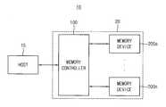
도 1은 본 발명의 실시예들에 따른 전자 시스템을 나타내는 블록도이다.1 is a block diagram illustrating an electronic system according to embodiments of the present invention.
도 1을 참조하면, 전자 시스템(10)은 호스트(15) 및 메모리 시스템(20)을 포함할 수 있다. 메모리 시스템(20)은 메모리 컨트롤러(100) 및 복수의 반도체 메모리 장치들(200a~200n)을 포함할 수 있다.Referring to Figure 1, the
호스트(15)는 PCI-E(Peripheral Component Interconnect - Express), ATA(Advanced Technology Attachment), SATA(Serial ATA), PATA(Parallel ATA), 또는 SAS(serial attached SCSI)와 같은 인터페이스 프로토콜을 사용하여 메모리 시스템(20)과 통신할 수 있다. 또한 호스트(15)와 메모리 시스템(20)간의 인터페이스 프로토콜들은 상술한 예에 한정되지 않으며, USB(Universal Serial Bus), MMC(Multi-Media Card), ESDI(Enhanced Small Disk Interface), 또는 IDE(Integrated Drive Electronics) 등과 같은 다른 인터페이스 프로토콜들 중 하나일 수 있다.The
메모리 컨트롤러(Memory Controller; 100)는 메모리 시스템(Memory System; 20)의 동작을 전반적으로 제어하며, 호스트(15)와 메모리 장치들(200a~200n) 사이의 전반적인 데이터 교환을 제어한다. 예컨대, 메모리 컨트롤러(100)는 호스트(15)의 요청에 따라 반도체 메모리 장치들(200a~200n)을 제어하여 데이터를 기입하거나(write) 데이터를 독출한다(read).A
또한, 메모리 컨트롤러(100)는 반도체 메모리 장치들(200a~200n)을 제어하기 위한 동작 커맨드(command)들을 인가하여, 반도체 메모리 장치들(200a~200n)의 동작을 제어한다.In addition, the
실시예에 따라, 반도체 메모리 장치들(200a~200n) 각각은 저항성 메모리 셀들을 구비하는 PRAM(Phase change Random Access Memory)이나, RRAM(Resistive Random Access Memory), MRAM(Magnetic Random Access Memory), 및 FRAM(Ferroelectric Random Access Memory) 일 수 있다. 다른 실시예에서, 반도체 메모리 장치들(200a~200n) 각각은 동적 메모리 셀들을 구비하는 DRAM(dynamic random access) 일 수 있다.Each of the
MRAM은 자기저항(magnetoresistance) 기반의 비휘발성 컴퓨터 메모리 기술이다. MRAM은 여러가지 면에서 휘발성 RAM과 다르다. MRAM은 비휘발성이기 때문에, 메모리 장치 전원이 오프되어도 MRAM은 메모리 내용을 유지할 수 있다.MRAM is a nonvolatile computer memory technology based on magnetoresistance. MRAM differs from volatile RAM in many ways. Since the MRAM is non-volatile, the MRAM can maintain the memory contents even when the memory device is powered off.
일반적으로 비휘발성 RAM이 휘발성 RAM 보다 느리다고 하지만, MRAM은 휘발성 RAM의 독출 및 기입 응답 시간들에 견줄만한 독출 및 기입 응답 시간을 갖는다. 전하로서 데이터를 저장하는 전형적인 RAM 기술과는 달리, MRAM 데이터는 자기저항 요소들에 의해 데이터를 저장한다. 일반적으로, 자기저항 요소들은 2개 자성층들로 이루어지고, 각 자성층은 자화(magnetization)를 가진다.Generally, non-volatile RAM is slower than volatile RAM, but MRAM has read and write response times comparable to volatile RAM read and write response times. Unlike a typical RAM technology for storing data as a charge, MRAM data stores data by magnetoresistive elements. Generally, the magnetoresistive elements are composed of two magnetic layers, and each magnetic layer has magnetization.
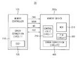
도 2는 본 발명의 실시예들에 따른 도 1의 메모리 시스템의 개략적인 구성을 나타내는 블록도이다.Figure 2 is a block diagram illustrating a schematic configuration of the memory system of Figure 1 in accordance with embodiments of the present invention.
도 2에서는 메모리 컨트롤러(100)에 대응되는 하나의 반도체 메모리 장치(200a)만을 예로 들어 설명한다.In FIG. 2, only one
도 2를 참조하면, 메모리 시스템(20)은 메모리 컨트롤러(100)와 반도체 메모리 장치(200a)를 포함할 수 있다. 메모리 컨트롤러(100)는 반도체 메모리 장치(200a)에 커맨드 신호(CMD) 및 어드레스 신호(ADDR)를 전송할 수 있다. 메모리 컨트롤러(100)와 반도체 메모리 장치(200a)는 메인 데이터(MD)와 메인 데이터(MD)에 기초하여 생성되고 메인 데이터(MD)의 에러를 정정하기 위한 패리티 데이터(PRT)를 교환할 수 있다.Referring to FIG. 2, the
메모리 컨트롤러(110)는 메인 데이터(MD)를 반도체 메모리 장치(200)에 전송할 때, 제1 에러 정정 코드(error correction code, 이하 'ECC')를 이용하여 패리티 데이터(PRT)를 생성하는 제1 에러 정정 회로(120)를 포함할 수 있다.The
반도체 메모리 장치(200a)는 메인 데이터(MD)와 패리티 데이터(PRT)가 저정되는 메모리 셀 어레이(300)이 및 메모리 셀 어레이에 대한 액세스를 제어하는 제어 로직 회로(210)를 포함할 수 있다. 또한 반도체 메모리 장치(200a)는 메모리 컨트롤러(100)로부터의 커맨드(CMD)가 내부 연산 동작을 지시하는 경우에 선택적으로 활성화되어 메모리 셀 어레이(300)에 저장된 데이터(비트 벡터)에 대하여 내부 연산을 수행하는 내부 연산 회로(360)와 상기 내부 연산의 결과를 나타내는 연산 결과 데이터에 대하여 ECC 인코딩을 수행하여 제2 패리티 데이터를 생성하고 상기 내부 연산 데이터와 상기 제2 패리티 데이터를 메모리 셀 어레이(300)의 타겟 페이지에 저장하는 제2 에러 정정 회로(400)를 포함할 수 있다.The
제2 에러 정정 회로(400)는 내부에 저장된 복수의 ECC들 중 상기 제1 ECC(120)와 동일한 ECC를 이용하여 상기 제2 패리티 데이터를 생성할 수 있다.The second
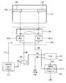
도 3은 본 발명의 실시예들에 따른 도 2의 반도체 메모리 장치의 구성을 나타내는 블록도이다.3 is a block diagram showing the configuration of the semiconductor memory device of FIG. 2 according to the embodiments of the present invention.
도 3을 참조하면, 반도체 메모리 장치(200a)는 제어 로직 회로(또는 제어 로직, 210), 어드레스 레지스터(220), 뱅크 제어 로직(230), 리프레쉬 카운터(297), 로우 어드레스 멀티플렉서(240), 컬럼 어드레스 래치(250), 로우 디코더(260), 컬럼 디코더(270), 메모리 셀 어레이(300), 센스 앰프부(285), 입출력 게이팅 회로(290), 내부 연산 회로(390), 제2 에러 정정 회로(400), 경로 선택 회로(280) 및 데이터 입출력 버퍼(299)를 포함할 수 있다.3, the
반도체 메모리 장치(200a)는 내부 연산 회로(390)를 포함하여 팝 카운팅 및 논리 비트 연산들의 인-메모리 실행(processing in memory, PIM)을 지원할 수 있다. 또한 반도체 메모리 장치(200a)는 상기 인-메모리 실행을 수행하는 경우에 인-메모리 실행의 결과에 대하여 ECC 인코딩을 수행하는, 복수의 ECC들을 포함하는 제2 에러 정정 회로(400)를 포함하여 메모리 컨트롤러(100)가 제조자에 의하여 달라져도 메모리 컨트롤러(100)의 제1 ECC(120)와 동일한 ECC를 사용하여 상기 ECC 인코딩을 수행할 수 있다. 즉 제2 에러 정정 회로(400)의 ECC는 구성가능(configurable)하다.
실시예에 따라서, 리프레쉬 카운터(297)는 반도체 메모리 장치(200a)에 포함되지 않을 수도 있다.According to the embodiment, the
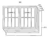
상기 메모리 셀 어레이(300)는 제1 내지 제8 뱅크 어레이들(310~380)을 포함할 수 있다. 또한, 상기 로우 디코더(260)는 제1 내지 제8 뱅크 어레이들(310~380)에 각각 연결된 제1 내지 제8 뱅크 로우 디코더들(260a~260h)을 포함하고, 상기 컬럼 디코더(270)는 제1 내지 제8 뱅크 어레이들(310~380)에 각각 연결된 제1 내지 제8 뱅크 컬럼 디코더들(270a~270h)을 포함하며, 상기 센스 앰프부(285)는 제1 내지 제8 뱅크 어레이들(310~380)에 각각 연결된 제1 내지 제4 뱅크 센스 앰프들(285a~285h)을 포함할 수 있다. 제1 내지 제8 뱅크 어레이들(310~380), 제1 내지 제8 뱅크 센스 앰프들(285a~285h), 제1 내지 제8 뱅크 칼럼 디코더들(270a~270h) 및 제1 내지 제8 뱅크 로우 디코더들(260a~260h)은 제1 내지 제8 뱅크들을 각각 구성할 수 있다. 제1 내지 제8 뱅크 어레이들(310~380) 각각은 복수의 워드라인(WL)들과 복수의 비트라인(BTL)들 및 워드라인(WL)들과 비트라인(BTL)들이 교차하는 지점에 형성되는 복수의 메모리 셀(MC)들을 포함할 수 있다. 도 3에는 8개의 뱅크들을 포함하는 반도체 메모리 장치(200a)의 예가 도시되어 있으나, 실시예에 따라, 반도체 메모리 장치(200a)는 임의의 수의 뱅크들을 포함할 수 있다.The memory cell array 300 may include first to
어드레스 레지스터(220)는 메모리 컨트롤러(100)로부터 뱅크 어드레스(BANK_ADDR), 로우 어드레스(ROW_ADDR) 및 컬럼 어드레스(COL_ADDR)를 포함하는 어드레스(ADDR)를 수신할 수 있다. 어드레스 레지스터(220)는 수신된 뱅크 어드레스(BANK_ADDR)를 뱅크 제어 로직(230)에 제공하고, 수신된 로우 어드레스(ROW_ADDR)를 로우 어드레스 멀티플렉서(240)에 제공하며, 수신된 컬럼 어드레스(COL_ADDR)를 컬럼 어드레스 래치(250)에 제공할 수 있다.The
뱅크 제어 로직(230)은 뱅크 어드레스(BANK_ADDR)에 응답하여 뱅크 제어 신호들을 생성할 수 있다. 상기 뱅크 제어 신호들에 응답하여, 제1 내지 제8 뱅크 로우 디코더들(260a~260h) 중 뱅크 어드레스(BANK_ADDR)에 상응하는 뱅크 로우 디코더가 활성화되고, 제1 내지 제8 뱅크 컬럼 디코더들(270a~270h) 중 뱅크 어드레스(BANK_ADDR)에 상응하는 뱅크 컬럼 디코더가 활성화될 수 있다.The
리프레쉬 카운터(297)는 제어 로직 회로(210)로부터의 제어에 따라 메모리 셀 어레이(300)에 포함되는 메모리 셀 로우들을 리프레쉬하기 위한 리프레쉬 로우 어드레스(REF_ADDR)를 생성할 수 있다. 리프레쉬 카운터(297)는 메모리 셀(MC)등이 동적 메모리 셀들로 구성되는 경우에 반도체 메모리 장치(200a)에 포함될 수 있다.The
로우 어드레스 멀티플렉서(240)는 어드레스 레지스터(220)로부터 로우 어드레스(ROW_ADDR)를 수신하고, 리프레쉬 카운터(297)로부터 리프레쉬 로우 어드레스(REF_ADDR)를 수신할 수 있다. 로우 어드레스 멀티플렉서(240)는 로우 어드레스(ROW_ADDR) 또는 리프레쉬 로우 어드레스(REF_ADDR)를 로우 어드레스(RA)로서 선택적으로 출력할 수 있다. 로우 어드레스 멀티플렉서(245)로부터 출력된 로우 어드레스(RA)는 제1 내지 제8 뱅크 로우 디코더들(260a~260h)에 각각 인가될 수 있다.The
제1 내지 제8 뱅크 로우 디코더들(260a~260h) 중 뱅크 제어 로직(230)에 의해 활성화된 뱅크 로우 디코더는 로우 어드레스 멀티플렉서(240)로부터 출력된 로우 어드레스(RA)를 디코딩하여 상기 로우 어드레스에 상응하는 워드 라인을 활성화할 수 있다. 예를 들어, 상기 활성화된 뱅크 로우 디코더는 로우 어드레스에 상응하는 워드 라인에 워드 라인 구동 전압을 인가할 수 있다.The bank row decoder activated by the
컬럼 어드레스 래치(250)는 어드레스 레지스터(220)로부터 컬럼 어드레스(COL_ADDR)를 수신하고, 수신된 컬럼 어드레스(COL_ADDR)를 일시적으로 저장할 수 있다. 또한, 컬럼 어드레스 래치(250)는, 버스트 모드에서, 수신된 컬럼 어드레스(COL_ADDR)를 점진적으로 증가시킬 수 있다. 컬럼 어드레스 래치(250)는 일시적으로 저장된 또는 점진적으로 증가된 컬럼 어드레스(COL_ADDR)를 제1 내지 제8 뱅크 컬럼 디코더들(270a~270h)에 각각 인가할 수 있다.The
제1 내지 제8 뱅크 컬럼 디코더들(270a~270h) 중 뱅크 제어 로직(230)에 의해 활성화된 뱅크 컬럼 디코더는 입출력 게이팅 회로(290)를 통하여 뱅크 어드레스(BANK_ADDR) 및 컬럼 어드레스(COL_ADDR)에 상응하는 센스 앰프를 활성화시킬 수 있다.The bank column decoder activated by the
입출력 게이팅 회로(290)는 입출력 데이터를 게이팅하는 회로들과 함께, 입력 데이터 마스크 로직, 제1 내지 제8 뱅크 어레이들(310~380)로부터 출력된 데이터를 저장하기 위한 독출 데이터 래치들, 및 제1 내지 제8 뱅크 어레이들(310~380)에 데이터를 기입하기 위한 기입 드라이버들을 포함할 수 있다. 또한 입출력 게이팅 회로(290)는 메인 데이터와 패리티 데이터의 저장 위치를 변경하는 크로스바 스위치를 포함할 수 있다.The input /
제1 내지 제8 뱅크 어레이들(310~380) 중 하나의 뱅크 어레이에서 독출될 데이터는 상기 하나의 뱅크 어레이에 상응하는 센스 앰프에 의해 감지되고, 상기 독출 데이터 래치들에 저장될 수 있다. 상기 독출 데이터 래치들에 저장된 데이터는 내부 연산 모드에 따라 내부 연산 회로(390)와 에러 정정 회로(400)를 선택적으로 경유하고 데이터 입출력 버퍼(299)를 통하여 메모리 컨트롤러(100)에 제공될 수 있다. 제1 내지 제8 뱅크 어레이들(310~380) 중 하나의 뱅크 어레이에 기입될 코드 워드(CW)는 상기 메모리 컨트롤러(100)로부터 데이터 입출력 버퍼(299)에 제공될 수 있다. 데이터 입출력 버퍼(299)에 제공된 메인 데이터(MD)는 상기 기입 드라이버들을 통하여 상기 하나의 뱅크 어레이에 기입될 수 있다.Data to be read out from one of the bank arrays of the first to
데이터 입출력 버퍼(299)는 기입 동작에서는 메모리 컨트롤러(100)로부터 제공되는 메인 데이터(MD)를 입출력 게이팅 회로(290)에 제공하고, 독출 동작에서는 에러 정정 회로(400)로부터 제공되는 제2 코드워드(CW2)나 경로 선택 회로(280)로부터 제공되는 제1 코드워드(CW1)를 메모리 컨트롤러(100)에 제공할 수 있다.The data input /
경로 선택 회로(280)는 내부 연산 모드 신호(IPS)에 응답하여 노멀 모드에서는 입출력 게이팅 회로(290)로부터의 제1 코드워드(CW1)를 데이터 입출력 버퍼(299)에 제공하고, 내부 연산 모드에서는 입출력 게이팅 회로(290)로부터의 제1 코드워드(CW1)를 내부 연산 회로(290)에 제공할 수 있다.The
내부 연산 회로(390)는 내부 연산 모드 신호(IPS)에 응답하여 선택적으로 활성화되어 내부 연산 모드에서 경로 선택 회로(280)로부터 제공되는 제1 코드워드(CW1)의 메인 데이터에 대하여 내부 연산을 수행하고, 상기 내부 연산의 수행 결과인 연산 결과 데이터를 에러 정정 회로(400)에 제공할 수 있다.The
에러 정정 회로(400)는 제2 제어 신호(CTL2)에 응답하여 내부 연산 모드에서는 연산 결과 데이터에 대하여 ECC 인코딩을 수행하여 제2 패리티 데이터를 생성하고, 상기 연산 결과 데이터와 제2 패리티 데이터를 포함하는 제2 코드워드(CW2)를 입출력 게이팅 회로(290)를 통하여 타겟 페이지에 저장할 수 있다. 또한 에러 정정 회로(400)는 제2 코드워드(CW2)를 데이터 입출력 버퍼(299)를 통하여 메모리 컨트롤러(100)에 전송할 수 있다.The
제어 로직 회로(210)는 반도체 메모리 장치(200a)의 동작을 제어할 수 있다. 예를 들어, 제어 로직 회로(210)는 반도체 메모리 장치(200a)가 기입 동작 또는 독출 동작을 수행하도록 제어 신호들을 생성할 수 있다. 제어 로직 회로(210)은 상기 메모리 컨트롤러(100)로부터 수신되는 커맨드(CMD)를 디코딩하는 커맨드 디코더(211) 및 반도체 메모리 장치(200a)의 동작 모드를 설정하기 위한 모드 레지스터(212)를 포함할 수 있다.The
예를 들어, 커맨드 디코더(211)는 기입 인에이블 신호(/WE), 로우 어드레스 스트로브 신호(/RAS), 컬럼 어드레스 스트로브 신호(/CAS), 칩 선택 신호(/CS) 등을 디코딩하여 커맨드(CMD)에 상응하는 상기 제어 신호들을 생성할 수 있다. 특히 제어 로직 회로(210)는 커맨드(CMD)를 디코딩하여 입출력 게이팅 회로(290)를 제어하는 제1 제어 신호(CTL1)와 에러 정정 회로(400)를 제어하는 제2 제어 신호(CTL2)를 생성할 수 있다. 제어 로직 회로(210)의 모드 레지스터(212)는 커맨드(CMD)에 의하여 내부 연산 모드로 설정되는 경우, 내부 연산 모드 신호(IPS)를 제1 로직 레벨로 출력할 수 있다. 제어 로직 회로(210)는 내부 연산 모드 신호(IPS)를 경로 선택 회로(280)와 내부 연산 회로(390)에 제공할 수 있다.For example, the
도 4a 내지 도 4e는 도 3에 도시된 메모리 셀을 예시적으로 나타내는 회로도들이다.4A to 4E are circuit diagrams exemplarily showing the memory cell shown in FIG.
도 4a 내지 도 4d에서는 도 3의 메모리 셀(MC)이 저항성 메모리 셀로 구현된 경우를 나타내고, 도 4e는 도 3의 메모리 셀(MC)이 동적 메모리 셀로 구현된 경우를 나타낸다.4A to 4D show a case where the memory cell MC of FIG. 3 is implemented as a resistive memory cell, and FIG. 4E shows a case where the memory cell MC of FIG. 3 is implemented as a dynamic memory cell.
도 4a는 선택 소자가 없는 저항성 메모리 셀을 나타낸다. 도 4b 내지 도 4d는 선택 소자를 포함하는 저항성 메모리 셀을 나타낸다.Figure 4A shows a resistive memory cell without a selection element. Figures 4B-4D show a resistive memory cell comprising a selection device.
도 4a를 참조하면, 메모리 셀(MC)은 비트 라인(BTL) 및 워드 라인(WL)에 연결되는 저항성 소자(RE)를 포함한다. 이처럼 선택 소자가 없는 구조를 갖는 저항성 메모리 셀은 비트 라인(BTL)과 워드 라인(WL) 사이에 인가되는 전압에 의해서 데이터를 저장한다.Referring to FIG. 4A, a memory cell MC includes a resistive element RE connected to a bit line BTL and a word line WL. The resistive memory cell having such a structure without a selection element stores data by a voltage applied between the bit line BTL and the word line WL.
도 4b를 참조하면, 메모리 셀(MC)은 저항성 소자(RE)와 다이오드(D)를 포함한다. 저항성 소자(RE)는 데이터를 저장하기 위한 저항성 물질을 포함한다. 다이오드(D)는 워드 라인(WL) 및 비트 라인(BTL)의 바이어스에 따라 저항성 소자(RE)에 전류를 공급 또는 차단하는 선택 소자(또는, 스위칭 소자)이다. 다이오드(D)는 저항성 소자(RE)와 워드 라인(WL) 사이에 연결되며, 저항성 소자(RE)는 비트 라인(BTL)과 다이오드(D) 사이에 연결된다. 다이오드(D)와 저항성 소자(RE)의 위치는 서로 바뀔 수 있다. 다이오드(D)는 워드 라인(WL) 전압에 의해 턴온 또는 턴오프 된다. 따라서, 비선택된 워드 라인(WL)에 일정 레벨 이상의 전압을 제공하면, 저항성 메모리 셀은 구동되지 않는다.Referring to FIG. 4B, the memory cell MC includes a resistive element RE and a diode D. The resistive element RE includes a resistive material for storing data. The diode D is a selection element (or a switching element) that supplies or cuts off the current to the resistive element RE according to the bias of the word line WL and the bit line BTL. The diode D is connected between the resistive element RE and the word line WL and the resistive element RE is connected between the bit line BTL and the diode D. The positions of the diode D and the resistive element RE may be changed from each other. Diode D is turned on or off by the word line (WL) voltage. Therefore, when a voltage higher than a certain level is supplied to the unselected word line WL, the resistive memory cell is not driven.
도 4c를 참조하면, 메모리 셀(MC)은 저항성 소자(RE)와 양방향 다이오드(BD)를 포함한다. 저항성 소자(RE)는 데이터를 저장하기 위한 저항성 물질을 포함한다. 양방향 다이오드(BD)는 저항성 소자(RE)와 워드 라인(WL) 사이에 연결되며, 저항성 소자(RE)는 비트 라인(BTL)과 양방향 다이오드(BD) 사이에 연결된다. 양방향 다이오드(BD)와 저항성 소자(RE)의 위치는 서로 바뀔 수 있다. 양방향 다이오드(BD)는 비선택 저항성 메모리 셀에 흐르게 되는 누설 전류를 차단할 수 있다.Referring to FIG. 4C, the memory cell MC includes a resistive element RE and a bi-directional diode BD. The resistive element RE includes a resistive material for storing data. The bidirectional diode BD is connected between the resistive element RE and the word line WL and the resistive element RE is connected between the bit line BTL and the bidirectional diode BD. The positions of the bidirectional diode BD and the resistive element RE may be mutually changed. The bidirectional diode BD can block the leakage current flowing in the non-selective resistive memory cell.
도 4d를 참조하면, 메모리 셀(MC)은 저항성 소자(RE)와 트랜지스터(CT)를 포함한다. 트랜지스터(CT)는 워드 라인(WL)의 전압에 따라 저항성 소자(RE)에 전류를 공급 또는 차단하는 선택 소자(또는, 스위칭 소자)이다. 트랜지스터(CT)는 저항성 소자(RE)와 워드 라인(WL) 사이에 연결되며, 저항성 소자(R)는 비트 라인(BTL)과 트랜지스터(CT) 사이에 연결된다. 트랜지스터(CT)와 저항성 소자(RE)의 위치는 서로 바뀔 수 있다. 메모리 셀(MC)은 워드 라인(WL)에 의해서 구동되는 트랜지스터(CT)의 온-오프 여부에 따라 선택 또는 비선택될 수 있다.Referring to FIG. 4D, the memory cell MC includes a resistive element RE and a transistor CT. The transistor CT is a selection element (or a switching element) that supplies or cuts off the current to the resistive element RE according to the voltage of the word line WL. The transistor CT is connected between the resistive element RE and the word line WL and the resistive element R is connected between the bit line BTL and the transistor CT. The positions of the transistor CT and the resistive element RE may be switched from each other. The memory cell MC may be selected or unselected depending on whether the transistor CT driven by the word line WL is turned on or off.
도 4e를 참조하면, 메모리 셀(MC)은 셀 커패시터(CC)와 트랜지스터(CT)를 포함한다. 트랜지스터(CT)는 워드 라인(WL)의 전압에 따라 셀 커패시터(CC)를 비트라인에 연결 또는 차단하는 선택 소자이다. 트랜지스터(CT)는 셀 커패시터(CC)와 워드라인(WL)과 비트라인(BTL) 사이에 연결되며, 셀 커패시터(CC)는 트랜지스터(CT)와 플레이트 전압(미도시) 사이에 연결된다.Referring to FIG. 4E, the memory cell MC includes a cell capacitor CC and a transistor CT. The transistor CT is a selection device that connects or disconnects the cell capacitor CC to the bit line in accordance with the voltage of the word line WL. The transistor CT is connected between the cell capacitor CC and the word line WL and the bit line BTL and the cell capacitor CC is connected between the transistor CT and the plate voltage (not shown).
도 5는 본 발명의 실시예들에 따른 도 3의 반도체 메모리 장치에서 메모리 셀의 예를 나타낸다.Figure 5 shows an example of a memory cell in the semiconductor memory device of Figure 3 according to embodiments of the present invention.
도 5를 참조하면, 메모리 셀(MC)은 STT-MRAM 셀(30)로 구성될 수 있고, STT-MRAM 셀(30)은 MTJ 소자(40)와 셀 트랜지스터(CT)를 포함할 수 있다. 셀 트랜지스터(CT)의 게이트는 워드라인(WL)에 연결되고, 셀 트랜지스터(CT)의 제1 전극은 MTJ 소자(40)를 통해 비트라인(BTL)에 연결된다. 또한 셀 트랜지스터(CT)의 제2 전극은 소스라인(SL)에 연결된다.Referring to FIG. 5, a memory cell MC may be composed of an STT-
MTJ 소자(40)는 자유 층(41)과 고정 층(43) 및 이들 사이에 터널 층(42)을 포함할 수 있다. 고정 층(43)의 자화 방향은 고정되어 있으며, 자유 층(41)의 자화 방향은 기입된 데이터에 따라 고정 층(43)의 자화 방향과 평행이거나 반-평행 방향이 될 수 있다. 고정 층(43)의 자화 방향을 고정시켜 주기 위하여, 예컨대, 반강자성층(anti-ferromagnetic layer, 미도시)이 더 구비될 수 있다.The
STT-MRAM 셀(30)의 기입 동작을 하기 위해서, 워드라인(WL)에 로직 하이의 전압을 인가하여 셀 트랜지스터(CT)를 턴 온시킨다. 비트라인(BL)과 소스 라인(SL)에는 프로그램 전류, 즉 기입 전류가 인가된다. 기입 전류의 방향은 MTJ 소자(40)에 기입될 로직 상태에 의해 결정된다.In order to perform the write operation of the STT-
STT-MRAM 셀의 독출 동작을 하기 위해서, 워드라인(WL)에 로직 하이의 전압을 주어 셀 트랜지스터(CT)를 턴 온시키고, 비트라인(BL)과 소스라인(SL0)으로 독출 전류를 인가한다. 이에 따라, MTJ 소자(40) 양단으로 전압이 디벨롭되고, 센스 앰프(285a)에 의해 센싱되고, MTJ 소자(40)에 기입된 로직 상태를 결정하기 위한 기준 전압과 비교된다. 이에 따라, MTJ 소자(40)에 저장된 데이터를 판별할 수 있다.In order to perform the read operation of the STT-MRAM cell, the cell transistor CT is turned on by applying a logic high voltage to the word line WL, and a read current is applied to the bit line BL and the source line SL0 . Thereby, the voltage is developed at both ends of the
도 6은 비-내부 연산 모드(노멀 모드)에서의 도 3의 반도체 메모리 장치의 일부를 나타낸다.FIG. 6 shows a part of the semiconductor memory device of FIG. 3 in the non-internal operation mode (normal mode).
도 6에서는 제어 로직 회로(210), 제1 뱅크 어레이(310), 입출력 게이팅 회로(290), 경로 선택 회로(280), 내부 연산 회로(390) 및 제2 에러 정정 회로(400)가 도시되어 있다.6, a
도 6을 참조하면, 노멀 모드에서는 내부 연산 모드 신호(IPS)가 제2 로직 레벨(로우 레벨)을 가지게 되어 내부 연산 회로(390)는 비활성화된다. 제1 뱅크 어레이(310)는 워드라인들과 비트라인들의 교차점에 연결되는 복수의 메모리 셀들을 포함하고, 상기 메모리 셀들은 동적 메모리 셀 또는 저항성 메모리 셀들로 구성될 수 있다.Referring to FIG. 6, in the normal mode, the internal operation mode signal IPS has the second logic level (low level), and the
입출력 게이팅 회로(290)는 제1 뱅크 어레이(310)와 연결되는 크로스-바 스위치(293) 및 크로스-바 스위치(293)와 연결되는 복수의 스위칭 회로들(291a~291d)를 포함할 수 있다. 복수의 스위칭 회로들(291a~291d)은 경로 선택 회로(280) 및 데이터 입출력 버퍼(299)에 연결될 수 있다. 반도체 메모리 장치(200a)에서 비트라인들은 액세스할 수 있는 칼럼 로케이션의 최대 수를 나타내는 버스트 길이(burst length, BL)를 지원하기 위하여 버스트 길이에 해당하는 비트라인들이 동시에 액세스될 수 있다. 반도체 메모리 장치(200a)는 예시적으로 버스트 길이가 8로 설정될 수 있다. 이에 따라 비트라인들은 128개의 칼럼 선택 신호들 각각에 연결되는 칼럼 선택부에 각각 연결되고 하나의 칼럼 선택부에 의하여 8개의 비트라인들이 동시에 선택될 수 있다.The input /
노멀 모드의 기입 동작에서 데이터 입출력 버퍼 회로(299)로부터의 제1 코드워드(CW1)가 스위칭 회로들(291a~291d)에 제공될 수 있다. 스위칭 회로들(291a~291d)는 제1 제어 신호(CTL1)에 응답하여 제1 코드워드(CW1)를 크로스-바 스위치(293)에 제공할 수 있다. 크로스-바 스위치(293)는 제1 제어 신호(CTL1)에 응답하여 제1 코드워드(CW1)를 제1 뱅크 어레이(CW1)의 타겟 페이지(TPG)에 전달할 수 있다. 크로스-바 스위치(293)는 제1 제어 신호(CTL1)에 응답하여 제1 코드워드(CW1)를 제1 뱅크 어레이(CW1)의 타겟 페이지(TPG)에 전달함에 있어, 크로스-바 스위치(293)는 제1 코드워드(CW1)의 제1 패리티 데이터를 타겟 페이지(TPG)의 상위 어드레스 영역(UAR) 또는 하위 어드레스 영역(LAR)에 전달할 수 있다.The first code word CW1 from the data input /
크로스-바 스위치(293)가 제1 코드워드(CW1)의 제1 패리티 데이터를 타겟 페이지(TPG)의 상위 어드레스 영역(UAR)에 전달하는 경우, 제1 코드워드(CW1)의 제1 메인 데이터는 타겟 페이지(TPG)의 상위 어드레스 영역(UAR)을 제외한 나머지 영역에 저장될 수 있다. 크로스-바 스위치(293)가 제1 코드워드(CW1)의 제1 패리티 데이터를 타겟 페이지(TPG)의 하위 어드레스 영역(LAR)에 전달하는 경우, 제1 코드워드(CW1)의 제1 메인 데이터는 타겟 페이지(TPG)의 하위 어드레스 영역(LAR)을 제외한 나머지 영역에 저장될 수 있다.When the
노멀 모드의 독출 동작에서 타겟 페이지(TPG)로부터의 제1 코드워드(CW1)가 입출력 게이팅 회로(290)를 통하여 경로 선택 회로(280)에 제공할 수 있다. 경로 선택 회로(280)는 내부 연산 모드 신호(IPS)에 응답하여 제1 코드워드(CW1)를 데이터 입출력 버퍼(299)에 제공할 수 있다.The first code word CW1 from the target page TPG can be provided to the
도 7은 내부 연산 모드에서 도 3의 반도체 메모리 장치의 일부를 나타낸다.FIG. 7 shows a part of the semiconductor memory device of FIG. 3 in the internal operation mode.
도 7의 내부 연산 모드에서의 기입 동작은 도 6의 노멀 모드의 기입 동작과 실질적으로 동일하므로 이에 대한 상세한 설명은 생략한다.Since the write operation in the internal operation mode of FIG. 7 is substantially the same as the write operation of the normal mode of FIG. 6, a detailed description thereof will be omitted.
도 7을 참조하면, 내부 연산 모드의 독출 동작에서 입출력 게이팅 회로(290)는 타겟 페이지(TPG)에 저장된 제1 코드워드(CW1)를 경로 선택 회로(280)에 제공하고, 경로 선택 회로(280)는 내부 연산 모드 신호(IPS)에 응답하여 제1 코드워드(CW1)를 내부 연산 회로(390)에 제공한다. 내부 연산 회로(390)는 내부 연산 모드 신호(IPS)에 응답하여 활성화되고, 제1 코드워드(CW1)의 제1 메인 데이터에 대하여 상응하는 내부 연산을 수행하여 연산 결과 데이터(MD2)를 제2 에러 정정 회로(400)에 제공한다. 내부 연산 회로(390)는 도 16에 도시된 바와 같이, 적어도 하나의 버퍼(391) 및 적어도 하나의 연산 블록(393)을 포함할 수 있다.7, the input /
제2 에러 정정 회로(400)는 연산 결과 데이터(MD2)에 대하여 ECC 인코딩을 수행하여 제2 패리티 데이터를 생성하고, 연산 결과 데이터(MD2)와 제2 패리티 데이터를 포함하는 제2 코드워드(CW2)를 입출력 게이팅 회로(290)와 데이터 입출력 버퍼(299)에 제공한다.The second
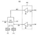
도 8은 본 발명의 실시예들에 따른 도 3의 반도체 메모리 장치에서 제2 에러 정정 회로의 구성을 나타내는 블록도이다.8 is a block diagram showing a configuration of a second error correction circuit in the semiconductor memory device of FIG. 3 according to the embodiments of the present invention.
도 8을 참조하면, 제2 에러 정정 회로(400)는 ECC 엔진(420), 버퍼부(440) 및 복수의 저장 소자들(471~47k)를 포함하여 구성될 수 있다. 버퍼부(440)는 제1 버퍼(441) 및 제2 버퍼(443)을 포함할 수 있다.Referring to FIG. 8, the second
제1 버퍼(441)은 모드 신호(MS)에 응답하여 내부 연산 모드의 독출 동작에서 활성화되고, 연산 결과 데이터(MD2)를 ECC 엔진(420)에 제공할 수 있다. 제2 버퍼(443)는 모드 신호(MS)에 응답하여 노멀 모드의 독출 동작에서 활성화되고, 제1 코드워드(CW1)를 ECC 엔진(420)에 제공할 수 있다.The
ECC 엔진(420)은 선택 신호(SS)에 응답하여 저장 소자들(SD1~SDk)에 저장된 복수의 ECC들 중에서 도 1의 제1 ECC(120)와 동일한 ECC를 선택하여 ECC 인코딩과 ECC 디코딩을 수행할 수 있다. 특히 ECC 엔진(420)은 내부 연산 모드의 독출 동작에서 상기 선택된 동일한 ECC를 이용하여 연산 결과 데이터(MD2)에 대하여 ECC 인코딩을 수행하여 제2 패리티 데이터(PRT2)를 생성하고 연산 결과 데이터(MD2)와 제2 패리티 데이터(PRT2)를 포함하는 제2 코드워드(CW2)를 입출력 게이팅 회로(290)와 데이터 입출력 버퍼(299)에 제공할 수 있다.The
예를 들어, 도 2의 메모리 컨트롤러(100)의 제1 ECC(120)가 SEC(single error correction) 코드이면, 메모리 컨트롤러(100)는 내부 연산 커맨드에 제1 ECC(120)의 정보를 포함하여 제어 로직 회로(210)로 전송할 수 있고, 제어 로직 회로(210)의 커맨드 디코더(211)는 제1 ECC(120)의 정보를 나타내는 선택 신호(SS)를 포함하는 제2 제어 신호(CTL2)를 에러 정정 회로(400)에 제공할 수 있다. ECC 엔진(420)은 선택 신호(SS)에 응답하여 제1 ECC(120)와 동일한 ECC(ECCa)를 선택하여 ECC 인코딩을 수행할 수 있다.For example, if the
예를 들어, 도 2의 메모리 컨트롤러(100)의 제1 ECC(120)가 SECDED(single error correction and double erorr detection) 코드이면, ECC 엔진(420)은 선택 신호(SS)에 응답하여 제1 ECC(120)와 동일한 ECC(ECCb)를 선택하여 ECC 인코딩을 수행할 수 있다. 예를 들어, 도 2의 메모리 컨트롤러(100)의 제1 ECC(120)가 DEC(double error correction 코드이면, ECC 엔진(420)은 선택 신호(SS)에 응답하여 제1 ECC(120)와 동일한 ECC(ECCc)를 선택하여 ECC 인코딩을 수행할 수 있다.For example, if the
도 9는 본 발명의 실시예들에 따른 도 9의 에러 정정 회로에서 ECC 엔진을 나타낸다.Figure 9 shows an ECC engine in the error correction circuit of Figure 9 according to embodiments of the present invention.
도 9를 참조하면, ECC 엔진(420)은 ECC 인코더(425)를 ECC 디코더(430)를 포함할 수 있다.Referring to FIG. 9, the
ECC 디코더(425)는 노멀 모드의 독출 동작에서 제1 코드워드(CW1)에 대하여 ECC 디코딩을 수행하여 정정된 코드워드(C_CW1)를 입출력 데이터 버퍼(299)에 제공할 수 있다. ECC 인코더(430)는 내부 연산 모드의 독출 동작에서 선택 신호(SS1)에 응답하여 저장 소자들(SD1~SDk)에 저장된 복수의 ECC들 중에서 도 1의 제1 ECC(120)와 동일한 ECC를 선택하고, 상기 동일한 ECC를 이용하여 연산 결과 데이터(MD2)에 대하여 ECC 인코딩을 수행하여 연산 결과 데이터(MD2)와 제2 패리티 데이터(PRT2)를 포함하는 제2 코드워드(CW2)를 입출력 게이팅 회로(290)와 데이터 입출력 버퍼(299)에 제공할 수 있다.The
상술한 바와 같이, 본 발명의 실시예들에 따르면, 반도체 메모리 장치(200a)가 인-메모리 프로세싱을 지원함으로써 메모리-컨트롤러 인터페이스를 통한 전송을 크게 감소시킴으로써 메모리 밴드대역(bandwidth)를 절약할 수 있고, 복수의 ECC들 중 메모리 컨트롤러의 제1 ECC와 동일한 ECC를 사용하여 제2 패리티 데이터를 생성함으로써 반도체 메모리 장치(200a)의 효용성을 증가시킬 수 있다.As described above, according to the embodiments of the present invention,
도 10은 본 발명의 실시예들에 따른 메모리 시스템을 나타내는 도면이다.10 is a diagram illustrating a memory system in accordance with embodiments of the present invention.
도 10을 참조하면, 메모리 시스템(500)은 메모리 컨트롤러(30) 및 반도체 메모리 장치(40)를 포함한다. 반도체 메모리 장치(40)는 커맨드-어드레스 입출력 블록(AWORD)(41), 데이터 입출력 블록들(DWORD0~DWORD3)(42~45) 및 내부 회로(50)를 포함할 수 있다. 메모리 컨트롤러(30)는 커맨드-어드레스 입출력 블록(31), 데이터 입출력 블록들(32) 및 내부 회로(35)를 포함할 수 있다. 일 실시예에서, 반도체 메모리 장치(40)는 고 대역폭 메모리(HBM) 표준에 부합하는 메모리 장치일 수 있다.Referring to FIG. 10, the
메모리 컨트롤러(30)의 커맨드-어드레스 입출력 블록(31)으로부터 메모리 장치(40)의 커맨드-어드레스 입출력 블록(41)으로, 커맨드(CMD), 어드레스(ADDR), 시스템 클록 신호(CLK), 클록 인에이블 신호(CKE) 등이 전달될 수 있다. 한편 메모리 컨트롤러(30)의 데이터 입출력 블록들(32)과 반도체 메모리 장치(40)의 데이터 입출력 블록들(42~45) 사이에서 데이터(DQ), 패리티 데이터(PRT), 데이터 버스 인버젼 신호(DBI), 데이터 마스크 신호(DM), 기입 데이터 스트로브 신호(WDQS), 독출 데이터 스트로브 신호(RDQS) 등이 전달될 수 있다.The address ADDR, the system clock signal CLK, and the clock signal CLK from the command-address input /
다중-입력 쉬프트 레지스터(MISR: multiple-input shift register) 및/또는 선형 피드백 쉬프트 레지스터(LFSR: linear feedback shift register) 회로는 반도체 메모리 장치(40)의 입출력 블록들(41~45)에 구현될 수 있다. 이러한 MISR/LFSR 회로들은 메모리 컨트롤러(30)와 반도체 메모리 장치(40) 사이의 링크를 테스트하고 트레이닝하기 위해 구비될 수 있다.A multiple-input shift register (MISR) and / or a linear feedback shift register (LFSR) circuit may be implemented in the input / output blocks 41 to 45 of the
예를 들어, 도 10에 도시된 바와 같이, 데이터 입출력 블록들(42~45)에 포함되는 하나의 바이트에 상응하는 MISR/LFSR 회로는 20 비트의 크기를 가질 수 있다. 상기 20 비트는 바이트 데이터 신호, 패리티 신호, 데이터 버스 인버젼(DBI: data bus inversion) 신호 및 데이터 마스트(DM: data mask) 신호의 상승 비트들(R) 및 하강 비트들(F)을 포함할 수 있다. 커맨드-어드레스 입출력 블록(41)은 30 비트의 크기를 가질 수 있다. 상기 30 비트는 로우 코맨드의 6 비트들(R0~R5), 컬럼 코맨드의 8 비트들(C0~C7) 및 클록 인에이블 신호(CKE)의 상승 비트들(R) 및 하강 비트들(F)을 포함할 수 있다.For example, as shown in FIG. 10, the MISR / LFSR circuit corresponding to one byte included in the data input / output blocks 42 to 45 may have a size of 20 bits. The 20 bits include rising bits (R) and falling bits (F) of a byte data signal, a parity signal, a data bus inversion (DBI) signal and a data mast (DM) . The command-address input /
예를 들어, 하나의 채널에는 각각이 하나의 워드에 상응하는 4개의 데이터 입출력 블록들(42~45)이 포함될 수 있고 하나의 데이터 입출력 블록은 4 바이트(BYTE0~BYTE3)에 상응하는 4개의 MISR/LFSR 회로들을 포함할 수 있다.For example, one channel may include four data input / output blocks 42 to 45, each corresponding to one word, and one data input / output block may include four MISRs corresponding to four bytes (BYTE0 to BYTE3) / LFSR circuits.
내부 회로(50)는 도 3의 반도체 메모리 장치(200a)로 구현되어 내부 연산 회로와 제2 에러 정정 회로를 포함할 수 있고, 내부 회로(35)는 도 2에서와 같이 제1 에러 정정 회로를 포함할 수 있다. 따라서 메모리 시스템(500)에서는 반도체 메모리 장치(40)가 인-메모리 프로세싱을 지원함으로써 메모리-컨트롤러 인터페이스를 통한 전송을 크게 감소시킴으로써 메모리 밴드대역(bandwidth)를 절약할 수 있고, 복수의 ECC들 중 메모리 컨트롤러의 제1 ECC와 동일한 ECC를 사용하여 제2 패리티 데이터를 생성함으로써 반도체 메모리 장치(40)의 효용성을 증가시킬 수 있다.The
도 11은 고 대역폭 메모리의 구조의 일 예를 나타내는 도면이다.11 is a diagram showing an example of the structure of a high-bandwidth memory.
도 11을 참조하면, 고 대역폭 메모리(HBM)(600)는 복수의 DRAM 반도체 다이들(620, 630, 640, 650)이 적층된 구조를 포함할 수 있다. 고 대역폭 메모리는 채널이라 칭하는 복수의 독립된 인터페이스들을 통하여 상기 적층된 구조의 고 대역폭 동작에 최적화될 수 있다. HBM 표준에 따라서 각각의 DRAM 스택은 최대 8개의 채널까지 지원할 수 있다. 도 11에는 4개의 DRAM 반도체 다이들이 적층되고 각각의 DRAM 반도체 다이가 2개의 채널(CHANNEL0, CHANNEL1)을 지원하는 예가 도시되어 있다. 각각의 반도체 다이는 상기 적층 구조에 추가적인 커패시티(capacity) 및 추가적인 채널을 제공할 수 있다.Referring to FIG. 11, a high bandwidth memory (HBM) 600 may include a structure in which a plurality of DRAM semiconductor dies 620, 630, 640 and 650 are stacked. The high bandwidth memory may be optimized for high bandwidth operation of the stacked structure through a plurality of independent interfaces, referred to as channels. According to HBM standards, each DRAM stack can support up to eight channels. FIG. 11 shows an example in which four DRAM semiconductor dies are stacked and each DRAM semiconductor die supports two channels (CHANNEL0, CHANNEL1). Each semiconductor die may provide additional capacity and additional channels to the stack structure.
각각의 채널은 DRAM 뱅크들의 독립된 세트에 대한 액세스를 제공한다. 하나의 채널로부터의 리퀘스트는 다른 채널에 부착된 데이터를 액세스하지 못한다. 채널들은 독립적으로 클록킹되고 서로 동기화될 필요가 없다.Each channel provides access to an independent set of DRAM banks. A request from one channel does not access data attached to another channel. Channels are independently clocked and do not need to be synchronized with each other.
고 대역폭 메모리(600)는 스택 구조의 하부에 위치하고 신호의 재분배 및 다른 기능들을 제공하는 인터페이스 다이(610)를 선택적으로 포함할 수 있다. DRAM 반도체 다이들(620, 630, 640, 650)에 통상적으로 구현되는 기능들이 이러한 인터페이스 다이(610) 또는 로직 다이에 구현될 수 있다. 인터페이스 다이(610)에는 도 3을 참조하여 설명한 내부 연산 회로와 제2 에러 정정 회로가 구현되어 상술한 내부 연산 동작과 제2 패리티 생성 동작을 수행할 수 있다.The
도 12는 본 발명의 실시예들에 따른 반도체 메모리 장치를 나타내는 구조도이다.12 is a structural view showing a semiconductor memory device according to embodiments of the present invention.
도 12에 도시된 바와 같이, 반도체 메모리 장치(700)는 다수의 반도체 레이어들(LA1 내지 LAs, s는 3이상의 자연수)을 구비할 수 있으며, 가장 아래에 위치하는 반도체 레이어(LA1)는 마스터 칩인 것으로 가정하며 또한 나머지 반도체 레이어들(LA2 내지 LAs)은 슬레이브 칩인 것으로 가정한다. 다수의 반도체 레이어들(LA1 내지 LAs)은 관통 실리콘 비아(TSV)를 통해 신호를 서로 송수신하며, 마스터 칩(LA1)은 외면에 형성된 도전 수단(미도시)을 통해 외부의 메모리 컨트롤러(미도시)와 통신한다. 마스터 칩으로서 제1 반도체 레이어(710)와 슬레이브 칩으로서 제s 반도체 레이어(720)를 중심으로 하여 반도체 메모리 장치(700)의 구성 및 동작을 설명하면 다음과 같다.12, the
제1 반도체 레이어(710)는 슬레이브 칩들에 구비되는 메모리 영역(Memory region, 721)을 구동하기 위한 각종 주변 회로들을 구비한다. 예컨데, 제1 반도체 레이어(710)는 메모리의 워드라인을 구동하기 위한 로우 드라이버(X-Driver, 7101)와, 메모리의 비트라인을 구동하기 위한 칼럼 드라이버(Y-Driver, 7102)와, 데이터의 입출력을 제어하기 위한 데이터 입출력부(7103), 외부로부터 커맨드(CMD)를 입력받아 버퍼링하는 커맨드 버퍼(7104)와, 외부로부터 어드레스를 입력받아 버퍼링하는 어드레스 버퍼(7105) 등을 구비할 수 있다. 메모리 영역은 도 3을 참조하여 설명한 바와 같이 복수의 뱅크 어레이들을 포함할 수 있다.The
또한 제1 반도체 레이어(710)는 제어 로직(6107)을 더 포함할 수 있다. 제어 로직(6107)은 메모리 컨트롤러(미도시)로부터 제공되는 커맨드 및 어드레스 신호에 기초하여 메모리 영역(721)에 대한 액세스를 제어하고, 제어 신호들을 생성할 수 있다.The
한편, 제s 반도체 레이어(720)는, 외부로부터의 커맨드(CMD)가 내부 연산 모드를 지시하는 경우 메모리 영역(721)에 저장된 제1 코드워드에 대항 내부 연산을 수행하여 연산 결과 데이터를 생성하는 내부 연산 회로(623) 및 상기 연산 결과 데이터에 대하여 ECC 인코딩을 수행하여 제2 패리티 데이터를 생성하는 에러 정정 회로(622)를 포함할 수 있다. 에러 정정 회로(622)는 복수의 ECC들 중 상기 제1 코드워드의 패리티 데이터의 생성에 이용된 ECC와 동일한 ECC를 선택하고 상기 선택된 동일한 ECC를 이용하여 상기 ECC 인코딩을 수행할 수 있다. 따라서 메모리 컨트롤러가 변경되어 메모리 컨트롤러에 포함되는 에러 정정 회로의 ECC가 변경되어도 이와 동일한 ECC를 선택하여 ECC 인코딩을 수행함으로써 반도체 메모리 장치(700)의 효용성을 높일 수 있다.On the other hand, when the command CMD from the outside indicates the internal operation mode, the
또한 반도체 메모리 장치(700)에는 3차원 메모리 어레이가 제공될 수 있다. 상기 3차원 메모리 어레이는 실리콘 기판 상에 배치된 액티브 이ㅕ역을 구비하는 하나 이상의 물리적 레벨의 메모리 셀 어레이들 및 상기 메모리 셀들의 동작과 관련된 회로들이 모놀리딕(monolithic) 방식으로 형성될 수 있다. 여기서 'monolithic'이라는 용어는 복수의 레이어들로 구성된 어레이의 각 레벨이 하위 레이어 위에 직접적으로 적층되는 것을 의미한다. 본 발명에 참조로서 포함되는 다음의 특허 문헌들은 상기 3차원 메모리 어레이 대한 적절한 구성들을 기술한다. 상기 3차원 메모리 어레이에서 워드라인들 및/또는 비트라인들이 레벨들 사이에서 공유된다. 상기 특허문헌들은 다음과 같다: 미국 등록 특허 7,679,133; 8,553,466; 8,654,587; 8,559,235; 및 미국 공개 특허 2011/0233648.Further, the
도 13은 본 발명의 실시예들에 따른 반도체 메모리 장치의 동작 방법을 나타내는 흐름도이다.13 is a flowchart illustrating a method of operating a semiconductor memory device according to embodiments of the present invention.
도 2 내지 도 13을 참조하면, 워드라인들과 비트라인들에 연결된 복수의 메모리 셀들을 구비하는 메모리 셀 어레이(300) 및 메모리 셀 어레이(300)에 대한 액세스를 제어하는 제어 로직 회로(210)를 포함하는 반도체 메모리 장치(200a)의 동작 방법에서는, 메모리 셀 어레이(300)에 저장된 비트 벡터들에 대한 팝-카운트 연산을 수행하기 위한 내부 연산 명령(CMD)을 상기 제어 로직 회로(210)가 상기 메모리 컨트롤러(100)부터 수신한다(S210). 내부 연산 명령(CMD)과 함께 메모리 셀 어레이(300)의 타겟 페이지를 지정하는 어드레스(ADDR)가 메모리 컨트롤러(100)로부터 반도체 메모리 장치(200a)에 전송된다.2 to 13, a memory cell array 300 including a plurality of memory cells connected to word lines and bit lines, a
반도체 메모리 장치(200a)의 로우 디코더(260)와 입출력 게이팅 회로(290)는 상기 타겟 페이지에 저장된, 메인 데이터와 제1 패리티 데이터를 포함하는 비트 벡터를 내부 연산 회로(390)에 제공한다. 내부 연산 회로(390)는 상기 메인 데이터에 대하여 상기 내부 연산 명령(CMD)에 상응하는 연산을 수행하고, 상기 연산의 수행 결과인 연산 결과 데이터를 에러 정정 회로(400)에 제공한다(S120).The
에러 정정 회로(400)는 상기 연산 결과 데이터를 기초로 제2 패리티 데이터를 생성한다(S130). 에러 정정 회로(400)는 복수의 ECC들 중 상기 제1 패리티 데이터가 생성될 때 이용된 제1 ECC와 동일한 ECC를 선택하고 상기 선택된 동일한 ECC를 이용하여 상기 연산 결과 데이터에 대하여 ECC 인코딩을 수행하여 상기 제2 패리티 데이터를 생성한다.The
에러 정정 회로(400)는 상기 연산 결과 데이터와 상기 제2 패리티 데이터를 포함하는 제2 코드워드를 입출력 게이팅 회로(290)를 통하여 메모리 셀 어레이(300)의 상기 타겟 페이지에 저장한다(S140).The
에러 정정 회로(400)는 상기 연산 결과 데이터와 상기 제2 패리티 데이터를 포함하는 제2 코드워드를 데이터 입출력 버퍼(299)를 통하여 상기 메모리 컨트롤러(100)에 전송할 수 있다(S150).The
도 14는 본 발명의 실시예들에 따른 도 13의 동작 방법에서 팝-카운트 연산의 인-메모리 실행을 보다 상세히 나타내는 흐름도이다.Figure 14 is a flow diagram illustrating in-memory execution of a pop-count operation in more detail in the method of operation of Figure 13 in accordance with embodiments of the present invention.
팝-카운트 연산을 수행하기 위하여, 내부 연산 회로(390)는 팝 카운트 연산을 수행하기 위하여 팝-카운트 연산을 초기화한다(S121). 팝-카운트 연산을 초기화하는 것은 내부 연산 회로(390)에 포함되는 레지스터 등을 리셋하는 것을 포함할 수 있다.To perform the pop-count operation, the
내부 연산 회로(390)는 메모리 셀 어레이(300)의 타겟 페이지로부터의 메인 데이터의 데이터 비트들 중 미리 정해진 작은 타입의 비트들에 대하여 팝 카운팅을 수행한다(S123). 그 후에 내부 연산 회로(390)는 중간 결과들을 누적하기 위하여 감소 트리를 사용하여 최종 팝 카운트를 생성한다(S125).The
복수의 DRAM 페이지들을 포괄하는 큰 벡터들에 대한 팝 카운트를 실행할 때에, 반도체 메모리 장치(200a)은 해당 벡터가 저장되어 있는 모든 페이지 주소들(page address)에 대한 정보를 알아야 할 필요가 있다. 따라서, 벡터의 제1 DRAM 페이지가 처리된 후에, 반도체 메모리 장치(200a)는 해당 벡터에 남아있는 다음 페이지들을 파악할 것이다. 예를 들어, 복수의 페이지들이 트래버스(traverse)될 필요가 있을 때, DMA(Direct Memory Access)과 유사한 매커니즘이 실행될 수 있다. 이러한 실행에 있어서, 해당 벡터가 차지하고 있는 DRAM 페이지들의 물리 주소들은, 예를 들어, 메모리 컨트롤러(100)에 의하여 반도체 메모리 장치(200a)에 전송될 수 있다. 이 후, 이러한 페이지들은, 예를 들어 도 3의 제어 로직 회로(210)와 같은, 반도체 메모리 장치(200a) 내의 내부 컨트롤러에 의하여 트래버스(traverse)될 것이다.When executing a pop count for large vectors covering a plurality of DRAM pages, the
도 15는 본 발명의 실시예들에 따른 반도체 메모리 장치의 동작 방법을 나타내는 흐름도이다.15 is a flowchart illustrating a method of operating a semiconductor memory device according to embodiments of the present invention.
도 2 내지 도 12 및 도 15를 참조하면, 워드라인들과 비트라인들에 연결된 복수의 메모리 셀들을 구비하는 메모리 셀 어레이(300) 및 메모리 셀 어레이(300)에 대한 액세스를 제어하는 제어 로직 회로(210)를 포함하는 반도체 메모리 장치(200a)의 동작 방법에서는, 메모리 셀 어레이(300)에 저장된 둘 또는 그 이상의 비트 벡터들에 대한 논리 비트 연산을 수행하기 위한 내부 연산 명령(CMD)을 상기 제어 로직 회로(210)가 상기 메모리 컨트롤러(100)부터 수신한다(S210). 내부 연산 명령(CMD)과 함께 메모리 셀 어레이(300)의 둘 또는 그 이상의 타겟 페이지들을 지정하는 어드레스(ADDR)가 메모리 컨트롤러(100)로부터 반도체 메모리 장치(200a)에 전송된다.2 to 12 and 15, a memory cell array 300 having a plurality of memory cells connected to word lines and bit lines and a control logic circuit 300 for controlling access to the memory cell array 300 (CMD) for performing a logical bit operation on two or more bit vectors stored in the memory cell array (300) in the operation method of the semiconductor memory device (200a) The
반도체 메모리 장치(200a)의 로우 디코더(260)와 입출력 게이팅 회로(290)는 상기 둘 또는 그 이상의 타겟 페이지들에 저장된, 메인 데이터와 제1 패리티 데이터를 포함하는 둘 또는 그 이상의 비트 벡터를 내부 연산 회로(390)에 제공한다. 내부 연산 회로(390)는 상기 메인 데이터에 대하여 상기 내부 연산 명령(CMD)에 상응하는 논리 비트 연산을 수행하고, 상기 연산의 수행 결과인 연산 결과 데이터를 에러 정정 회로(400)에 제공한다(S220). 상기 논리 비트 연산은 OR 연산, AND 연산, NOT 연산, NAND 연산, NOR 연산 및 XOR 연산 중 하나일 수 있다.The
에러 정정 회로(400)는 상기 연산 결과 데이터를 기초로 제2 패리티 데이터를 생성한다(S130). 에러 정정 회로(400)는 복수의 ECC들 중 상기 제1 패리티 데이터가 생성될 때 이용된 제1 ECC와 동일한 ECC를 선택하고 상기 선택된 동일한 ECC를 이용하여 상기 연산 결과 데이터에 대하여 ECC 인코딩을 수행하여 상기 제2 패리티 데이터를 생성한다.The
에러 정정 회로(400)는 상기 연산 결과 데이터와 상기 제2 패리티 데이터를 포함하는 제2 코드워드를 입출력 게이팅 회로(290)를 통하여 메모리 셀 어레이(300)의 지정된 페이지에 저장한다(S240).The
에러 정정 회로(400)는 상기 연산 결과 데이터와 상기 제2 패리티 데이터를 포함하는 제2 코드워드를 데이터 입출력 버퍼(299)를 통하여 상기 메모리 컨트롤러(100)에 전송할 수 있다(S250). 이 경우에 연산 결과 데이터와 제2 패리티 데이터는 동시에 상기 메모리 컨트롤러(100)에 전송될 수 있다. 또한 제2 패리티 데이터는 연산 결과 데이터가 전송된 후에 메모리 컨트롤러(100)에 전송될 수 있다.The
도 16은 본 발명의 실시예들에 따라 도 3의 반도체 메모리 장치에서 논리 비트 연산이 수행되는 예를 나타낸다.16 shows an example in which a logical bit operation is performed in the semiconductor memory device of FIG. 3 according to the embodiments of the present invention.
도 3, 도 7 및 도 16을 참조하면, 제1 뱅크 어레이(310)에 저장된 두 개의 8-비트 오퍼랜드들 사이의 논리 비트 연산에 있어서, 두 오퍼랜드들 중 어느 하나의 8 비트는 대응하는 감지 증폭기(285a)에 의하여 상응하는 메모리 셀들로부터 독출될 것이다. 이러한 독출 동작은 화살표(81)에 의하여 표시되어 있다. 감지 증폭기(285a)는 수신된 데이터 비트들을 제1 오퍼랜드를 위한 버퍼(391)로 전송할 것이다. 이러한 전송 동작은 화살표(82)에 의하여 표시되어 있다. 논리 비트 연산을 위한 제2 오퍼랜드는 감지 증폭기(285a)에 의하여 상응하는 메모리 셀들로부터 독출될 것이다. 독출된 데이터 비트들은 연산 블록(393)으로 직접 전송된다. 이러한 동작은 화살표(84)에 의하여 표시되어 있다.Referring to Figures 3, 7 and 16, in a logical bit operation between two 8-bit operands stored in the
연산 블록(393)은, 예를 들어, 메모리 컨트롤러(100)에 의하여 명령된 적절한 논리 비트 연산을 수행하기 위하여 필요한 로직들을 포함할 수 있다. 예를 들어, 연산 블록(393)은 팝 카운트 연산들을 수행하는 반도체 메모리 장치(200a)를 구성하는 일부 논리 유닛들 및 논리 회로를 공유할 수 있다. 이러한 논리 비트 연산은 OR 연산, AND 연산, NOT 연산, NAND 연산, NOR 연산 및 XOR 연산 중 하나일 수 있다. 제1 오퍼랜드와 제2 오퍼랜드 사이의 지정된 논리 비트 연산의 결과에 의하여 연산 블록(393)은 연산 결과 데이터를 생성하고, 연산 결과 데이터를 도 3의 에러 정정 회로(400)에 제공할 수 있다. 예를 들어, 제1 오퍼랜드는 '11010010'의 비트 벡터일 수 있고, 제2 오퍼랜드는 '10001111'의 비트 벡터일 수 있다. 이러한 두 개의 비트 벡터들 사이의 논리 비트 AND 연산에 있어서, 연산 블록(393)은 '1000001'의 연산 결과 데이터(85)를 에러 정정 회로(400)에 출력할 수 있다.The
도 17은 본 발명의 실시예들에 따른 메모리 시스템의 동작 방법을 나타내는 흐름도이다.17 is a flow chart illustrating a method of operating a memory system in accordance with embodiments of the present invention.
도 2 내지 도 12 및 도 17을 참조하면, 반도체 메모리 장치(200a) 및 반도체 메모리 장치(200a)를 제어하는 메모리 컨트롤러(100)를 포함하는 메모리 시스템(20)의 동작 방법에서는 반도체 메모리 장치(200a)가 메모리 컨트롤러(100)로부터 기입 커맨드(CMD), 어드레스(ADDR) 및 메인 데이터와 제1 패리티 데이터를 포함하는 제1 코드워드(CW1)를 수신한다(S310). 반도체 메모리 장치(200a)는 커맨드(CMD)에 따라 제1 코드워드(CW1)를 어드레스(ADDR)가 지정하는, 메모리 셀 어레이(300)의 타겟 페이지에 기입한다(S320).2 to 12 and 17, in the method of operating the
반도체 메모리 장치(200a)는 메모리 컨트롤러(100)로부터의 제2 커맨드(CMD)가 내부 연산 커맨드인지 여부를 판단한다(S330). 제2 커맨드(CMD)가 내부 연산 커맨드가 아니고 독출 커맨드인 경우(S330에서 NO), 반도체 메모리 장치(200a)는 타겟 페이지로부터 제1 코드워드(CW1)를 독출하고(S340), 독출된 제1 코드워드(CW1)를 메모리 컨트롤러(100)에 전송한다(S345).The
제2 커맨드(CMD)가 내부 연산 커맨드인 경우(S330에서 YES), 반도체 메모리 장치(200a)는 타겟 페이지로부터 제1 코드워드(CW1)를 독출하고 독출된 제1 코드워드(CW1)를 내부 연산 회로에 제공한다(S350). 내부 연산 회로(390)는 제1 코드워드의 메인 데이터에 대하여 내부 연산을 수행하여 연산 결과 데이터(MD2)를 생성하고, 연산 결과 데이터(MD2)를 에러 정정 회로(400)에 제공한다(S360).If the second command CMD is an internal operation command (YES in S330), the
에러 정정 회로(400)는 연산 결과 데이터(MD2)에 대하여 ECC 인코딩을 수행하여 제2 패리티 데이터를 생성하고, 제2 패리티 데이터와 연산 결과 데이터를 포함하는 제2 코드워드를 타겟 페이지에 기입한다(S370). 이 때, 에러 정정 회로(400)는, 복수의 ECC들 중에서 메모리 컨트롤러(100)가 제1 패리티 데이터를 생성할 때 이용한 제1 ECC와 동일한 ECC를 선택하여 상기 ECC 인코딩을 수행할 수 있다. 반도체 메모리 장치(200a)는 제2 코드워들(CW2)를 또한 메모리 컨트롤러(100)에 전송할 수 있다(S380).The
도 18은 본 발명의 실시예들에 따른 반도체 메모리 장치를 포함하는 패키지 구조를 나타내는 단면도이다.18 is a cross-sectional view showing a package structure including a semiconductor memory device according to embodiments of the present invention.
도 18에서는 응용 프로세서(820)와 고대역폭 메모리를 다이 대 다이(die-to-die)로 직접 연결한 반도체 패키지(800)를 나타낸다.18 shows a
도 18을 참조하면, 반도체 패키지(800)는 응용 프로세서(820)와 메모리 칩을 각각 패키지한 후에 다시 패키지 하는 PoP(Package on Package) 방식이 아닌, 관통 실리콘 비아(TSV) 기술을 이용하여 응용 프로세서(820)와 HBM(830)을 직접 연결한다. 반도체 패키지(800)는 인쇄회로기판(PCB, 810) 위에 응용 프로세서(820)을 형성하고, 응용 프로세서(820)와 HBM(830)을 관통 실리콘 비아(TSV)를 통해 연결한다.Referring to FIG. 18, the
응용 프로세서(810)는 제1 ECC를 이용하여 제1 패리티 데이터를 생성하는 제1 에러 정정 회로를 구비하는 메모리 컨트롤러(821)를 포함할 수 있고, HBM(830)은 내부 연산 회로와 제2 에러 정정 회로를 포함할 수 있다. 상기 내부 연산 회로와 상기 제2 에러 정정 회로는 내부 연산 모드에서 활성화되어 상술한 선택적 내부 연산 동작와 ECC 인코딩을 수행할 수 있다.The
도 19는 본 발명의 실시예에 따른 반도체 메모리 장치를 모바일 시스템에 응용한 예를 나타내는 블록도이다.19 is a block diagram showing an example of application of a semiconductor memory device according to an embodiment of the present invention to a mobile system.
도 19를 참조하면, 모바일 시스템(900)은 어플리케이션 프로세서(910), 통신(Connectivity)부(920), 사용자 인터페이스(930), 비휘발성 메모리 장치(940), 휘발성 메모리 장치(950) 및 파워 서플라이(960)를 포함한다. 어플리케이션 프로세서(910)는 메모리 컨트롤러(911)를 포함할 수 있다.19, the
어플리케이션 프로세서(910)는 인터넷 브라우저, 게임, 동영상 등을 제공하는 어플리케이션들을 실행할 수 있다. 통신부(920)는 외부 장치와 무선 통신 또는 유선 통신을 수행할 수 있다. 휘발성 메모리 장치(950)는 어플리케이션 프로세서(910)에 의해 처리되는 데이터를 저장하거나, 동작 메모리(Working Memory)로서 작동할 수 있다. 휘발성 메모리 장치(950)는 도 3의 반도체 메모리 장치(200a)로 구현될 수 있다.The
비휘발성 메모리 장치(940)는 모바일 시스템(900)을 부팅하기 위한 부트 이미지를 저장할 수 있다. 사용자 인터페이스(920)는 키패드, 터치 스크린과 같은 하나 이상의 입력 장치, 및/또는 스피커, 디스플레이 장치와 같은 하나 이상의 출력 장치를 포함할 수 있다. 파워 서플라이(960)는 모바일 시스템(900)의 동작 전압을 공급할 수 있다.
모바일 시스템(900) 또는 모바일 시스템(900)의 구성요소들은 다양한 형태들의 패키지를 이용하여 실장될 수 있다.The components of
상술한 바와 같이, 메모리 컨트롤러(911)는 제1 ECC를 이용하여 제1 패리티 데이터를 생성하는 제1 에러 정정 회로를 포함할 수 있고, 휘발성 메모리 장치(950)는 내부 연산 회로와 제2 에러 정정 회로를 포함할 수 있다. 상기 내부 연산 회로와 상기 제2 에러 정정 회로는 내부 연산 모드에서 활성화되어 상술한 선택적 내부 연산 동작와 ECC 인코딩을 수행할 수 있다.As described above, the
상술한 바와 같이, 본 발명의 실시예들에서는 반도체 메모리 장치가 인-메모리 프로세싱을 지원함으로써 메모리-컨트롤러 인터페이스를 통한 전송을 크게 감소시킴으로써 메모리 밴드대역(bandwidth)를 절약할 수 있고, 복수의 ECC들 중 메모리 컨트롤러의 제1 ECC와 동일한 ECC를 사용하여 제2 패리티 데이터를 생성함으로써 반도체 메모리 장치의 효용성을 증가시킬 수 있다.As described above, in the embodiments of the present invention, the semiconductor memory device can reduce in-memory bandwidth by greatly reducing transmission through the memory-controller interface by supporting in-memory processing, and a plurality of ECCs It is possible to increase the utility of the semiconductor memory device by generating the second parity data using the same ECC as that of the first ECC of the memory controller.
본 발명은 반도체 메모리 장치를 사용하는 시스템에 적용될 수 있다. 예를 들어, 본 발명은 휴대폰(Mobile Phone), 스마트 폰(Smart Phone), 개인 정보 단말기(personal digital assistant; PDA), 휴대형 멀티미디어 플레이어(portable multimedia player; PMP), 디지털 카메라(Digital Camera), 캠코더(Camcoder), 개인용 컴퓨터(Personal Computer; PC), 서버 컴퓨터(Server Computer), 워크스테이션(Workstation), 노트북(Laptop), 디지털 TV(Digital Television), 셋-탑 박스(Set-Top Box), 음악 재생기(Music Player), 휴대용 게임 콘솔(Portable Game Console), 네비게이션(Navigation) 시스템, 스마트 카드(Smart Card), 프린터(Printer) 등에 유용하게 이용될 수 있다.The present invention can be applied to a system using a semiconductor memory device. For example, the present invention can be applied to a mobile phone, a smart phone, a personal digital assistant (PDA), a portable multimedia player (PMP), a digital camera, a camcorder A computer, a camcoder, a personal computer (PC), a server computer, a workstation, a laptop, a digital television, a set-top box, A music player, a portable game console, a navigation system, a smart card, a printer, and the like.
상술한 바와 같이, 본 발명의 실시예들을 참조하여 설명하였지만, 해당 기술 분야에서 통상의 지식을 가진 자는 하기의 특허청구범위에 기재된 본 발명의 사상 및 영역으로부터 벗어나지 않는 범위 내에서 본 발명을 다양하게 수정 및 변경시킬 수 있음을 이해할 것이다.While the present invention has been described with reference to exemplary embodiments, it is to be understood that the invention is not limited to the disclosed exemplary embodiments, but, on the contrary, is intended to cover various modifications and equivalent arrangements included within the spirit and scope of the appended claims. It will be understood that the invention may be varied and changed without departing from the scope of the invention.
100: 메모리 컨트롤러 110: 제1 에러 정정 회로
200a: 반도체 메모리 장치 390: 내부 연산 회로
400: 제2 에러 정정 회로100: memory controller 110: first error correction circuit
200a: semiconductor memory device 390: internal operation circuit
400: second error correction circuit
Claims (20)
Translated fromKorean메모리 컨트롤러로부터의 커맨드에 응답하여 내부 연산의 수행 여부를 지시하는 내부 연산 모드 신호를 생성하는 제어 로직 회로;
상기 내부 연산 모드 신호에 응답하여 상기 메모리 셀 어레이로부터 독출된 비트 벡터에 대하여 선택적으로 내부 연산을 수행하여 연산 결과 데이터를 출력하는 내부 연산 회로; 및
상기 연산 결과 데이터에 대하여 에러 정정 코드(error correction code, 이하 'ECC') 인코딩을 수행하여 제2 패리티 데이터를 생성하고, 상기 연산 결과 데이터와 상기 제2 패리티 데이터를 상기 메모리 셀 어레이에 저장하는 에러 정정 회로를 포함하고,
상기 에러 정정 회로는 복수의 ECC들 중에서 상기 비트 벡터의 제1 패리티 데이터를 생성할 때 이용된 제1 ECC와 동일한 ECC를 선택하여 상기 제2 패리티 데이터를 생성하는 반도체 메모리 장치.A memory cell array including a plurality of memory cells coupled to word lines and bit lines;
A control logic circuit responsive to the command from the memory controller for generating an internal operation mode signal indicating whether to perform an internal operation;
An internal operation circuit for selectively performing an internal operation on a bit vector read from the memory cell array in response to the internal operation mode signal and outputting operation result data; And
And generates second parity data by performing error correction code (ECC) encoding on the operation result data and stores the operation result data and the second parity data in the memory cell array A correction circuit,
Wherein the error correction circuit selects the ECC equal to the first ECC used when generating the first parity data of the bit vector among a plurality of ECCs to generate the second parity data.
상기 복수의 ECC들을 각각 저장하는 복수의 저장 소자들; 및
상기 복수의 저장 소자들에 연결되고, 상기 복수의 ECC들 중에서 상기 제어 로직 회로로부터의 제어 신호에 응답하여 상기 동일한 ECC를 이용하여 상기 연산 결과 데이터에 대하여 상기 ECC 인코딩을 수행하여 상기 제2 패리티 데이터를 생성하는 ECC 엔진을 포함하는 반도체 메모리 장치.The apparatus of claim 1, wherein the error correction circuit
A plurality of storage elements for storing the plurality of ECCs, respectively; And
And an ECC encoding unit for performing ECC encoding on the operation result data using the same ECC in response to a control signal from the control logic circuit among the plurality of ECCs, And an ECC engine for generating an ECC engine.
상기 커맨드에 응답하여 설정되어 상기 내부 연산 모드 신호를 생성하는 모드 레지스터; 및
상기 커맨드를 디코딩하여 상기 에러 정정 회로를 제어하는 제어 신호를 생성하는 커맨드 디코더를 포함하는 반도체 메모리 장치.2. The method of claim 1, wherein the control logic circuit
A mode register set in response to the command to generate the internal operation mode signal; And
And a command decoder for decoding the command to generate a control signal for controlling the error correction circuit.
상기 메모리 셀 어레이와 상기 에러 정정 회로에 연결되는 입출력 게이팅 회로를 포함하고,
상기 입출력 게이팅 회로는 상기 제어 로직 회로로부터의 제어 신호에 응답하여 상기 메모리 셀 어레이에서 상기 제2 패리티 데이터가 저장되는 위치를 변경하는 반도체 메모리 장치.The method according to claim 1,
And an input / output gating circuit connected to the memory cell array and the error correction circuit,
Wherein the input / output gating circuit changes a position at which the second parity data is stored in the memory cell array in response to a control signal from the control logic circuit.
상기 입출력 게이팅 회로는 상기 제어 신호에 응답하여 상기 연산 결과 데이터와 상기 제2 패리티 데이터가 저장되는 상기 메모리 셀 어레이의 타겟 페이지의 하위 어드레스 영역에 상기 제2 패리티 데이터를 저장하고, 상기 하위 어드레스 영역을 제외한 나머지 영역에 상기 연산 결과 데이터를 저장하는 반도체 메모리 장치.5. The method of claim 4,
Wherein the input / output gating circuit stores the second parity data in a lower address area of a target page of the memory cell array in which the calculation result data and the second parity data are stored in response to the control signal, And stores the calculation result data in the remaining area.
상기 입출력 게이팅 회로는 상기 제어 신호에 응답하여 상기 연산 결과 데이터와 상기 제2 패리티 데이터가 저장되는 상기 메모리 셀 어레이의 타겟 페이지의 상위 어드레스 영역에 상기 제2 패리티 데이터를 저장하고 상기 상위 어드레스 영역을 제외한 나머지 영역에 반도체 메모리 장치.5. The method of claim 4,
Wherein the input / output gating circuit stores the second parity data in an upper address area of a target page of the memory cell array in which the calculation result data and the second parity data are stored in response to the control signal, And the remaining area is a semiconductor memory device.
상기 메모리 셀 어레이와 연결되는 크로스바 스위치; 및
상기 크로스바 스위치 및 상기 에러 정정 회로에 연결되고, 상기 연산 결과 데이터와 상기 제2 패리티 데이터를 상기 크로스바 스위치에 전달하는 복수의 스위치들을 포함하는 반도체 메모리 장치.5. The apparatus of claim 4, wherein the input / output gating circuit
A crossbar switch coupled to the memory cell array; And
And a plurality of switches connected to the crossbar switch and the error correction circuit, for transferring the calculation result data and the second parity data to the crossbar switch.
상기 에러 정정 회로는 데이터 입출력 버퍼를 통하여 상기 연산 결과 데이터와 상기 제2 패리티 데이터를 상기 메모리 컨트롤러에 전송하는 반도체 메모리 장치.The method according to claim 1,
Wherein the error correction circuit transmits the calculation result data and the second parity data to the memory controller via a data input / output buffer.
상기 내부 연산은 상기 메모리 셀 어레이의 하나의 타겟 페이지에 저장된 상기 비트 벡터에 대한 팝 카운트 연산인 반도체 메모리 장치.The method according to claim 1,
Wherein the internal operation is a pop count operation on the bit vector stored in one target page of the memory cell array.
상기 내부 연산은 상기 메모리 셀 어레이의 적어도 두개의 타겟 페이지들에 저장된 비트 벡터들에 대한 논리 비트 연산인 반도체 메모리 장치.The method according to claim 1,
Wherein the internal operation is a logical bit operation on bit vectors stored in at least two target pages of the memory cell array.
상기 논리 비트 연산은 OR 연산, AND 연산, NOT 연산, NAND 연산, NOR 연산 및 XOR 연산 중 하나인 반도체 메모리 장치.11. The method of claim 10,
Wherein the logical bit operation is one of an OR operation, an AND operation, a NOT operation, a NAND operation, a NOR operation, and an XOR operation.
상기 내부 연산 모드 신호에 응답하여 상기 비트 벡터를 상기 내부 연산 회로에 선택적으로 제공하는 경로 선택 회로를 더 포함하는 반도체 메모리 장치.
The method according to claim 1,
And a path selection circuit for selectively providing said bit vector to said internal arithmetic circuit in response to said internal operation mode signal.
상기 반도체 메모리 장치는 고 대역폭 메모리(high bandwidth memory)인 반도체 메모리 장치.The method according to claim 1,
Wherein the semiconductor memory device is a high bandwidth memory.
상기 적어도 하나의 반도체 메모리 장치를 제어하는 메모리 컨트롤러를 포함하고,
상기 메모리 컨트롤러는 제1 에러 정정 코드(error correction code, 이하 ECC)를 이용하여 기입 데이터에 대하여 ECC 인코딩을 수행하여 제1 패리티 데이터를 생성하고, 상기 기입 데이터와 상기 제1 패리티 데이터를 상기 적어도 하나의 반도체 메모리 장치에 전송하고,
상기 적어도 하나의 반도체 메모리 장치는
워드라인들 및 비트라인들에 연결되는 복수의 메모리 셀들을 포함하여 상기 기입 데이터와 상기 제1 패리티 데이터를 저장하는 메모리 셀 어레이;
상기 메모리 컨트롤러로부터의 커맨드에 응답하여 내부 연산의 수행 여부를 지시하는 내부 연산 모드 신호를 생성하는 제어 로직 회로;
상기 내부 연산 모드 신호에 응답하여 상기 메모리 셀 어레이로부터 독출된 상기 기입 데이터와 상기 제1 패리티 데이터를 포함하는 비트 벡터에 대하여 선택적으로 내부 연산을 수행하여 연산 결과 데이터를 출력하는 내부 연산 회로; 및
상기 연산 결과 데이터에 대하여 ECC 인코딩을 수행하여 제2 패리티 데이터를 생성하고, 상기 연산 결과 데이터와 상기 제2 패리티 데이터를 상기 메모리 셀 어레이에 저장하는 제1 에러 정정 회로를 포함하고,
상기 에러 정정 회로는 복수의 ECC들 중에서 상기 메모리 컨트롤러가 상기 제1 패리티 데이터를 생성할 때 이용한 제1 ECC와 동일한 ECC를 선택하여 상기 제2 패리티 데이터를 생성하는 메모리 시스템.At least one semiconductor memory device;
And a memory controller for controlling the at least one semiconductor memory device,
The memory controller performs ECC encoding on write data using a first error correction code (ECC) to generate first parity data, and writes the write data and the first parity data to the at least one To the semiconductor memory device,
The at least one semiconductor memory device
A memory cell array including a plurality of memory cells connected to word lines and bit lines to store the write data and the first parity data;
A control logic circuit responsive to a command from the memory controller for generating an internal operation mode signal indicating whether to perform an internal operation;
An internal operation circuit for selectively performing an internal operation on a bit vector including the write data and the first parity data read from the memory cell array in response to the internal operation mode signal and outputting operation result data; And
And a first error correction circuit for performing ECC encoding on the operation result data to generate second parity data and storing the operation result data and the second parity data in the memory cell array,
Wherein the error correction circuit selects the ECC equal to the first ECC used when the memory controller generates the first parity data among the plurality of ECCs to generate the second parity data.
상기 메모리 컨트롤러는 상기 기입 데이터에 대하여 상기 ECC 인코딩을 수행하여 상기 제1 패리티 데이터를 생성하는 제2 에러 정정 회로를 포함하는 메모리 시스템.15. The method of claim 14,
And the memory controller includes a second error correction circuit for performing the ECC encoding on the write data to generate the first parity data.
상기 메모리 컨트롤러는 상기 제1 패리티 데이터를 상기 기입 데이터와 동시에 상기 적어도 하나의 반도체 메모리 장치에 전송하는 메모리 시스템.15. The method of claim 14,
Wherein the memory controller transfers the first parity data to the at least one semiconductor memory device concurrently with the write data.
상기 메모리 컨트롤러는 상기 제1 패리티 데이터를 상기 기입 데이터를 전송한 후에 상기 적어도 하나의 반도체 메모리 장치에 전송하는 메모리 시스템.15. The method of claim 14,
Wherein the memory controller transfers the first parity data to the at least one semiconductor memory device after transmitting the write data.
상기 메모리 셀 어레이는 3차원 메모리 셀 어레이이고,
상기 복수의 메모리 셀들은 동적 메모리 셀들 또는 저항성 메모리 셀들인 메모리 시스템.15. The method of claim 14,
The memory cell array is a three-dimensional memory cell array,
Wherein the plurality of memory cells are dynamic memory cells or resistive memory cells.
상기 메모리 셀 어레이에 저장된 비트 벡터들에 대한 연산을 수행하기 위한 내부 연산 명령을 상기 제어 로직 회로가 상기 메모리 컨트롤러로부터 수신하는 단계;
상기 반도체 메모리 장치의 내부 연산 장치에서 상기 연산을 수행하여 연산 결과 데이터를 에러 정정 회로에 제공하는 단계;
상기 에러 정정 회로에서 상기 연산 결과 데이터를 기초로 패리티 데이터를 생성하는 단계;
상기 에러 정정 회로가 상기 연산 결과 데이터와 상기 패리티 데이터를 상기 메모리 셀 어레이의 타겟 페이지에 저장하는 단계; 및
상기 연산 결과 데이터와 상기 패리티 데이터를 상기 메모리 컨트롤러에 전송하는 단계를 포함하는 반도체 메모리 장치의 동작 방법.1. A method of operating a semiconductor memory device comprising a memory cell array having a plurality of memory cells connected to word lines and bit lines and a control logic circuit for controlling access to the memory cell array,
Receiving an internal operation instruction from the memory controller for the control logic circuit to perform an operation on bit vectors stored in the memory cell array;
Performing the arithmetic operation in an internal arithmetic unit of the semiconductor memory device and providing operation result data to an error correction circuit;
Generating parity data based on the operation result data in the error correction circuit;
The error correction circuit storing the calculation result data and the parity data in a target page of the memory cell array; And
And transferring the calculation result data and the parity data to the memory controller.
상기 연산은 상기 비트 벡터들에 대한 팝-카운트 연산 또는 상기 비트 벡터들에 대한 논리 비트 연산인 반도체 메모리 장치의 동작 방법.20. The method of claim 19,
Wherein the operation is a pop-count operation on the bit vectors or a logical bit operation on the bit vectors.
Priority Applications (3)
| Application Number | Priority Date | Filing Date | Title |
|---|---|---|---|
| KR1020160103992AKR102479212B1 (en) | 2016-08-17 | 2016-08-17 | Semiconductor memory device, memory system including the same and method of operating the same |
| US15/594,891US9953702B2 (en) | 2016-08-17 | 2017-05-15 | Semiconductor memory devices, memory systems including the same and methods of operating the same |
| CN201710695779.7ACN107767919B (en) | 2016-08-17 | 2017-08-15 | Semiconductor memory device, memory system including the same, and method of operating the same |
Applications Claiming Priority (1)
| Application Number | Priority Date | Filing Date | Title |
|---|---|---|---|
| KR1020160103992AKR102479212B1 (en) | 2016-08-17 | 2016-08-17 | Semiconductor memory device, memory system including the same and method of operating the same |
Publications (2)
| Publication Number | Publication Date |
|---|---|
| KR20180019818Atrue KR20180019818A (en) | 2018-02-27 |
| KR102479212B1 KR102479212B1 (en) | 2022-12-20 |
Family
ID=61192083
Family Applications (1)
| Application Number | Title | Priority Date | Filing Date |
|---|---|---|---|
| KR1020160103992AActiveKR102479212B1 (en) | 2016-08-17 | 2016-08-17 | Semiconductor memory device, memory system including the same and method of operating the same |
Country Status (3)
| Country | Link |
|---|---|
| US (1) | US9953702B2 (en) |
| KR (1) | KR102479212B1 (en) |
| CN (1) | CN107767919B (en) |
Cited By (9)
| Publication number | Priority date | Publication date | Assignee | Title |
|---|---|---|---|---|
| KR20210075930A (en)* | 2018-09-28 | 2021-06-23 | 타이완 세미콘덕터 매뉴팩쳐링 컴퍼니 리미티드 | Memory error detection and correction |
| KR20210093521A (en)* | 2020-01-20 | 2021-07-28 | 삼성전자주식회사 | High bandwidth memory and system having the same |
| CN113284531A (en)* | 2020-02-20 | 2021-08-20 | 三星电子株式会社 | Electronic system, stacked memory device and operation method thereof |
| KR20210118474A (en)* | 2019-02-19 | 2021-09-30 | 마이크론 테크놀로지, 인크 | Memory device with configurable internal error correction mode |
| KR20210134997A (en)* | 2019-03-29 | 2021-11-11 | 마이크론 테크놀로지, 인크. | Computational storage and network-based systems |
| US11204826B2 (en) | 2018-09-28 | 2021-12-21 | Taiwan Semiconductor Manufacturing Company, Ltd. | Memory error detection and correction |
| WO2022125545A1 (en)* | 2020-12-09 | 2022-06-16 | Advanced Micro Devices, Inc. | Programmable error correction code encoding and decoding logic |
| KR20230015536A (en)* | 2021-07-23 | 2023-01-31 | 삼성전자주식회사 | Data processing apparatus and method using direct memory access |
| US11681580B2 (en) | 2021-06-16 | 2023-06-20 | SK Hynix Inc. | Semiconductor system related to performing an error correction operation using an error correction method |
Families Citing this family (52)
| Publication number | Priority date | Publication date | Assignee | Title |
|---|---|---|---|---|
| US9997232B2 (en)* | 2016-03-10 | 2018-06-12 | Micron Technology, Inc. | Processing in memory (PIM) capable memory device having sensing circuitry performing logic operations |
| US10243584B2 (en)* | 2016-05-11 | 2019-03-26 | Samsung Electronics Co., Ltd. | Memory device including parity error detection circuit |
| US10346092B2 (en) | 2017-08-31 | 2019-07-09 | Micron Technology, Inc. | Apparatuses and methods for in-memory operations using timing circuitry |
| US10741239B2 (en) | 2017-08-31 | 2020-08-11 | Micron Technology, Inc. | Processing in memory device including a row address strobe manager |
| US10416927B2 (en) | 2017-08-31 | 2019-09-17 | Micron Technology, Inc. | Processing in memory |
| KR102370278B1 (en)* | 2017-11-30 | 2022-03-07 | 에스케이하이닉스 주식회사 | Memory controller, memory system including the same, and operation method thereof |
| US11119677B2 (en)* | 2017-12-15 | 2021-09-14 | Samsung Electronics Co., Ltd. | HBM based memory lookup engine for deep learning accelerator |
| JP2019109806A (en)* | 2017-12-20 | 2019-07-04 | ルネサスエレクトロニクス株式会社 | Data processing device and data processing method |
| KR102583797B1 (en)* | 2018-04-09 | 2023-10-05 | 에스케이하이닉스 주식회사 | Memory system and operating method of memory system |
| US11036578B2 (en)* | 2018-04-12 | 2021-06-15 | Samsung Electronics Co., Ltd. | Semiconductor memory devices and memory systems including the same |
| US10817372B2 (en)* | 2018-06-13 | 2020-10-27 | Innogrit Technologies Co., Ltd | Systems and methods for ultra fast ECC with parity |
| TWI715095B (en)* | 2018-07-03 | 2021-01-01 | 聯發科技股份有限公司 | Methods and memory systems of parity training for a dram |
| US10810078B2 (en)* | 2018-07-03 | 2020-10-20 | Mediatek Inc. | Method of parity training for a DRAM supporting a link error checking and correcting functionality |
| KR102728322B1 (en)* | 2018-08-10 | 2024-11-11 | 에스케이하이닉스 주식회사 | Memory system having ECC functionality for memory apparatus and method of operating the memory system |
| CN110942798B (en)* | 2018-09-25 | 2024-06-11 | 三星电子株式会社 | Semiconductor memory device, memory system, and method for operating a semiconductor memory device |
| WO2020099935A2 (en)* | 2018-10-04 | 2020-05-22 | Zafar Atif | Dynamic processing memory core on a single memory chip |
| KR102770731B1 (en)* | 2018-10-24 | 2025-02-24 | 삼성전자주식회사 | Memory modules and methods of operating memory systems |
| KR20200057475A (en)* | 2018-11-16 | 2020-05-26 | 삼성전자주식회사 | Memory device including arithmetic circuit and neural network system including the same |
| KR20200070686A (en)* | 2018-12-10 | 2020-06-18 | 에스케이하이닉스 주식회사 | Storage device and operating method thereof |
| KR102760198B1 (en)* | 2018-12-11 | 2025-02-04 | 삼성전자주식회사 | Memory system and operating method of memory system |
| US11138064B2 (en) | 2018-12-13 | 2021-10-05 | Micron Technology, Inc. | Dynamic control of error management and signaling |
| KR102674591B1 (en)* | 2019-01-15 | 2024-06-12 | 에스케이하이닉스 주식회사 | Command generation method and semiconductor device using the same |
| CN111679785B (en) | 2019-03-11 | 2025-03-11 | 三星电子株式会社 | Memory device for processing operation and operation method thereof, and data processing system |
| DE102020105628A1 (en) | 2019-03-11 | 2020-09-17 | Samsung Electronics Co., Ltd. | Method for performing internal processing operations with a predefined protocol interface of a storage device |
| DE102020106357A1 (en) | 2019-03-11 | 2020-09-17 | Samsung Electronics Co., Ltd. | STORAGE DEVICE AND INSTRUCTION RING STORAGE QUEUE PROCEDURE |
| US11094371B2 (en)* | 2019-03-11 | 2021-08-17 | Samsung Electronics Co., Ltd. | Memory device for processing operation and method of operating the same |
| US11080137B2 (en)* | 2019-05-09 | 2021-08-03 | Rambus Inc. | Error coalescing |
| CN110222006B (en)* | 2019-05-15 | 2023-10-20 | 杭州电子科技大学 | RRAM-based processor architecture and control method |
| WO2020258209A1 (en) | 2019-06-28 | 2020-12-30 | Yangtze Memory Technologies Co., Ltd. | Computation-in-memory in three-dimensional memory device |
| CN110476209B (en)* | 2019-06-28 | 2020-11-17 | 长江存储科技有限责任公司 | In-memory computation in three-dimensional memory devices |
| KR20210034999A (en)* | 2019-09-23 | 2021-03-31 | 에스케이하이닉스 주식회사 | AIM device and method of multiplying/accumulation in the AIM device |
| KR20210045875A (en)* | 2019-10-17 | 2021-04-27 | 에스케이하이닉스 주식회사 | Parity generating circuit for a plurality of error correction levels, memory controller and memory module including the parity generating circuit, and method for generating the parity |
| US11106530B2 (en)* | 2019-12-20 | 2021-08-31 | Micron Technology, Inc. | Parity protection |
| US11409600B2 (en)* | 2019-12-30 | 2022-08-09 | Micron Technology, Inc. | Increased memory access parallelism using parity |
| KR20210128224A (en)* | 2020-04-16 | 2021-10-26 | 에스케이하이닉스 주식회사 | Storage device and operating method thereof |
| US11237907B2 (en)* | 2020-05-29 | 2022-02-01 | Taiwan Semiconductor Manufacturing Company, Ltd. | Processing-in-memory instruction set with homomorphic error correction |
| KR20210149543A (en)* | 2020-06-02 | 2021-12-09 | 삼성전자주식회사 | Memory device and memory system including the same |
| US11322218B2 (en)* | 2020-06-08 | 2022-05-03 | Micron Technology, Inc. | Error control for memory device |
| US11449269B2 (en)* | 2020-07-22 | 2022-09-20 | Micron Technology, Inc. | Edge compute components under a memory array |
| KR20220032366A (en) | 2020-09-07 | 2022-03-15 | 삼성전자주식회사 | Memory device performing configurable mode set and Operating method thereof |
| US11409608B2 (en) | 2020-12-29 | 2022-08-09 | Advanced Micro Devices, Inc. | Providing host-based error detection capabilities in a remote execution device |
| US11573853B2 (en)* | 2021-03-31 | 2023-02-07 | Advanced Micro Devices, Inc. | Error checking data used in offloaded operations |
| KR20230043619A (en)* | 2021-09-24 | 2023-03-31 | 삼성전자주식회사 | Memory device and method of implementing reducing timimg parameters and power comsumption of internal processing operations |
| CN113793635B (en)* | 2021-11-08 | 2022-04-19 | 阿里云计算有限公司 | Storage device and storage apparatus |
| KR20230069316A (en)* | 2021-11-11 | 2023-05-19 | 삼성디스플레이 주식회사 | Display apparatus |
| TWI792754B (en)* | 2021-12-09 | 2023-02-11 | 力晶積成電子製造股份有限公司 | Memory device with high data bandwidth |
| US12374389B2 (en) | 2021-12-23 | 2025-07-29 | Changxin Memory Technologies, Inc. | Memory bank and memory |
| US12176054B2 (en) | 2021-12-23 | 2024-12-24 | Changxin Memory Technologies, Inc. | Memory bank and memory |
| CN116343891B (en)* | 2021-12-23 | 2025-06-20 | 长鑫存储技术有限公司 | Storage blocks and memory |
| US11869580B2 (en)* | 2021-12-30 | 2024-01-09 | Micron Technology, Inc. | Apparatuses, systems, and methods for counter-based read clock in stacked memory devices |
| CN114490172B (en)* | 2022-04-02 | 2022-07-12 | 武汉杰开科技有限公司 | Data storage system and method |
| US11822793B2 (en)* | 2022-04-04 | 2023-11-21 | Western Digital Technologies, Inc. | Complete and fast protection against CID conflict |
Citations (5)
| Publication number | Priority date | Publication date | Assignee | Title |
|---|---|---|---|---|
| US20040237023A1 (en)* | 2003-05-20 | 2004-11-25 | Nec Electronics Corporation | Memory device and memory error correction method |
| US20150135037A1 (en)* | 2012-03-06 | 2015-05-14 | Micron Technology, Inc. | Apparatuses and methods including error correction code organization |
| US20150309870A1 (en)* | 2007-05-12 | 2015-10-29 | Apple Inc. | Memory device with internal signal processing unit |
| KR20160039544A (en)* | 2014-10-01 | 2016-04-11 | 삼성전자주식회사 | In-memory popcount support for real time analytics |
| US9348539B1 (en)* | 2013-03-12 | 2016-05-24 | Inphi Corporation | Memory centric computing |
Family Cites Families (19)
| Publication number | Priority date | Publication date | Assignee | Title |
|---|---|---|---|---|
| JPH04248642A (en) | 1991-01-18 | 1992-09-04 | Kenneth W Iobst | Pim chip of memory integrated circuit and control method thereof |
| JPH08125640A (en)* | 1994-10-28 | 1996-05-17 | Murata Mach Ltd | Re-synchronization device for error correction coder decoder |
| US6631488B1 (en) | 2000-06-30 | 2003-10-07 | Agilent Technologies, Inc. | Configurable error detection and correction engine that has a specialized instruction set tailored for error detection and correction tasks |
| US8069377B2 (en) | 2006-06-26 | 2011-11-29 | Micron Technology, Inc. | Integrated circuit having memory array including ECC and column redundancy and method of operating the same |
| KR100855979B1 (en)* | 2007-02-13 | 2008-09-02 | 삼성전자주식회사 | Semiconductor memory device and parity data generation method for byte masking operation |
| US8122323B2 (en) | 2007-03-08 | 2012-02-21 | Intel Corporation | Method, apparatus, and system for dynamic ECC code rate adjustment |
| KR101425957B1 (en)* | 2007-08-21 | 2014-08-06 | 삼성전자주식회사 | Ecc control circuit and multi channel memory system icluding the same |
| JP2010003348A (en) | 2008-06-19 | 2010-01-07 | Toshiba Corp | Semiconductor memory device and error correction method |
| US8583898B2 (en) | 2009-06-12 | 2013-11-12 | Cray Inc. | System and method for managing processor-in-memory (PIM) operations |
| US8762813B2 (en) | 2010-05-17 | 2014-06-24 | Skymedi Corporation | Configurable coding system and method of multiple ECCS |
| US9337872B2 (en) | 2011-04-30 | 2016-05-10 | Rambus Inc. | Configurable, error-tolerant memory control |
| KR20130027138A (en)* | 2011-09-07 | 2013-03-15 | 삼성전자주식회사 | Method of correcting errors and memory device using the same |
| US8619451B1 (en)* | 2012-01-06 | 2013-12-31 | Netlogic Microsystems, Inc. | Power savings in a content addressable memory device using masked pre-compare operations |
| US9124300B2 (en)* | 2013-02-28 | 2015-09-01 | Sandisk Technologies Inc. | Error correction coding in non-volatile memory |
| US9281844B2 (en) | 2013-04-18 | 2016-03-08 | Apple Inc. | Configurable and low power encoder for cyclic error correction codes |
| US9164834B2 (en)* | 2013-05-06 | 2015-10-20 | Samsung Electronics Co., Ltd. | Semiconductor memory devices, memory systems including the same and method of writing data in the same |
| US10073731B2 (en)* | 2013-11-27 | 2018-09-11 | Intel Corporation | Error correction in memory |
| CN104733051B (en)* | 2013-12-19 | 2018-01-05 | 群联电子股份有限公司 | Decoding method of parity check code, memory storage device and control circuit unit |
| JP6212396B2 (en)* | 2014-01-08 | 2017-10-11 | ルネサスエレクトロニクス株式会社 | Data processing device |
- 2016
- 2016-08-17KRKR1020160103992Apatent/KR102479212B1/enactiveActive
- 2017
- 2017-05-15USUS15/594,891patent/US9953702B2/enactiveActive
- 2017-08-15CNCN201710695779.7Apatent/CN107767919B/enactiveActive
Patent Citations (5)
| Publication number | Priority date | Publication date | Assignee | Title |
|---|---|---|---|---|
| US20040237023A1 (en)* | 2003-05-20 | 2004-11-25 | Nec Electronics Corporation | Memory device and memory error correction method |
| US20150309870A1 (en)* | 2007-05-12 | 2015-10-29 | Apple Inc. | Memory device with internal signal processing unit |
| US20150135037A1 (en)* | 2012-03-06 | 2015-05-14 | Micron Technology, Inc. | Apparatuses and methods including error correction code organization |
| US9348539B1 (en)* | 2013-03-12 | 2016-05-24 | Inphi Corporation | Memory centric computing |
| KR20160039544A (en)* | 2014-10-01 | 2016-04-11 | 삼성전자주식회사 | In-memory popcount support for real time analytics |
Cited By (15)
| Publication number | Priority date | Publication date | Assignee | Title |
|---|---|---|---|---|
| US11762732B2 (en) | 2018-09-28 | 2023-09-19 | Taiwan Semiconductor Manufacturing Company, Ltd. | Memory error detection and correction |
| US12229003B2 (en) | 2018-09-28 | 2025-02-18 | Taiwan Semiconductor Manufacturing Company, Ltd. | Memory error detection and correction |
| KR20210075930A (en)* | 2018-09-28 | 2021-06-23 | 타이완 세미콘덕터 매뉴팩쳐링 컴퍼니 리미티드 | Memory error detection and correction |
| US11204826B2 (en) | 2018-09-28 | 2021-12-21 | Taiwan Semiconductor Manufacturing Company, Ltd. | Memory error detection and correction |
| KR20210118474A (en)* | 2019-02-19 | 2021-09-30 | 마이크론 테크놀로지, 인크 | Memory device with configurable internal error correction mode |
| KR20210134997A (en)* | 2019-03-29 | 2021-11-11 | 마이크론 테크놀로지, 인크. | Computational storage and network-based systems |
| US12175130B2 (en) | 2019-03-29 | 2024-12-24 | Micron Technology, Inc. | Computational storage and networked based system |
| KR20210093521A (en)* | 2020-01-20 | 2021-07-28 | 삼성전자주식회사 | High bandwidth memory and system having the same |
| KR20210106226A (en)* | 2020-02-20 | 2021-08-30 | 삼성전자주식회사 | Stacked memory device performing function-in-memory(FIM) operation and method of operating the same |
| CN113284531A (en)* | 2020-02-20 | 2021-08-20 | 三星电子株式会社 | Electronic system, stacked memory device and operation method thereof |
| CN113284531B (en)* | 2020-02-20 | 2025-08-08 | 三星电子株式会社 | Electronic system, stacked memory device and operating method thereof |
| US11734114B2 (en) | 2020-12-09 | 2023-08-22 | Advanced Micro Devices, Inc. | Programmable error correction code encoding and decoding logic |
| WO2022125545A1 (en)* | 2020-12-09 | 2022-06-16 | Advanced Micro Devices, Inc. | Programmable error correction code encoding and decoding logic |
| US11681580B2 (en) | 2021-06-16 | 2023-06-20 | SK Hynix Inc. | Semiconductor system related to performing an error correction operation using an error correction method |
| KR20230015536A (en)* | 2021-07-23 | 2023-01-31 | 삼성전자주식회사 | Data processing apparatus and method using direct memory access |
Also Published As
| Publication number | Publication date |
|---|---|
| CN107767919B (en) | 2021-02-19 |
| KR102479212B1 (en) | 2022-12-20 |
| US9953702B2 (en) | 2018-04-24 |
| CN107767919A (en) | 2018-03-06 |
| US20180053545A1 (en) | 2018-02-22 |
Similar Documents
| Publication | Publication Date | Title |
|---|---|---|
| KR102479212B1 (en) | Semiconductor memory device, memory system including the same and method of operating the same | |
| US10198221B2 (en) | Methods of operating semiconductor memory devices with selective write-back of data for error scrubbing and related devices | |
| US10868570B2 (en) | Error detection code generation circuits of semiconductor devices, memory controllers including the same and semiconductor memory devices including the same | |
| CN107393596B (en) | Semiconductor memory device and method of operating the same | |
| CN106971758B (en) | Semiconductor memory device, memory system, and method of operating memory system | |
| KR102766341B1 (en) | Memory module, memory system including the same and method of operating memory system | |
| US10127102B2 (en) | Semiconductor memory devices and memory systems including the same | |
| KR102324769B1 (en) | Error correction circuit, semiconductor memory device and memory system including the same | |
| US10191805B2 (en) | Semiconductor memory devices and memory systems including the same | |
| US10002045B2 (en) | Semiconductor memory devices having input/output gating circuit and memory systems including the same | |
| KR20170060263A (en) | Semiconductor memory device and method of operating the same |
Legal Events
| Date | Code | Title | Description |
|---|---|---|---|
| PA0109 | Patent application | Patent event code:PA01091R01D Comment text:Patent Application Patent event date:20160817 | |
| PG1501 | Laying open of application | ||
| A201 | Request for examination | ||
| PA0201 | Request for examination | Patent event code:PA02012R01D Patent event date:20210720 Comment text:Request for Examination of Application Patent event code:PA02011R01I Patent event date:20160817 Comment text:Patent Application | |
| E701 | Decision to grant or registration of patent right | ||
| PE0701 | Decision of registration | Patent event code:PE07011S01D Comment text:Decision to Grant Registration Patent event date:20221124 | |
| GRNT | Written decision to grant | ||
| PR0701 | Registration of establishment | Comment text:Registration of Establishment Patent event date:20221215 Patent event code:PR07011E01D | |
| PR1002 | Payment of registration fee | Payment date:20221216 End annual number:3 Start annual number:1 | |
| PG1601 | Publication of registration |