KR20180018497A - Vertical integration method and circuit element architecture for area scaling of semiconductor devices - Google Patents
Vertical integration method and circuit element architecture for area scaling of semiconductor devicesDownload PDFInfo
- Publication number
- KR20180018497A KR20180018497AKR1020177032875AKR20177032875AKR20180018497AKR 20180018497 AKR20180018497 AKR 20180018497AKR 1020177032875 AKR1020177032875 AKR 1020177032875AKR 20177032875 AKR20177032875 AKR 20177032875AKR 20180018497 AKR20180018497 AKR 20180018497A
- Authority
- KR
- South Korea
- Prior art keywords
- gate structures
- region
- gate
- semiconductor
- semiconductor fin
- Prior art date
- Legal status (The legal status is an assumption and is not a legal conclusion. Google has not performed a legal analysis and makes no representation as to the accuracy of the status listed.)
- Ceased
Links
Images


Classifications
- H—ELECTRICITY
- H10—SEMICONDUCTOR DEVICES; ELECTRIC SOLID-STATE DEVICES NOT OTHERWISE PROVIDED FOR
- H10D—INORGANIC ELECTRIC SEMICONDUCTOR DEVICES
- H10D88/00—Three-dimensional [3D] integrated devices
- H01L27/0688—
- H01L21/8221—
- H01L21/823821—
- H01L29/78—
- H—ELECTRICITY
- H10—SEMICONDUCTOR DEVICES; ELECTRIC SOLID-STATE DEVICES NOT OTHERWISE PROVIDED FOR
- H10B—ELECTRONIC MEMORY DEVICES
- H10B10/00—Static random access memory [SRAM] devices
- H10B10/12—Static random access memory [SRAM] devices comprising a MOSFET load element
- H—ELECTRICITY
- H10—SEMICONDUCTOR DEVICES; ELECTRIC SOLID-STATE DEVICES NOT OTHERWISE PROVIDED FOR
- H10B—ELECTRONIC MEMORY DEVICES
- H10B12/00—Dynamic random access memory [DRAM] devices
- H10B12/30—DRAM devices comprising one-transistor - one-capacitor [1T-1C] memory cells
- H10B12/36—DRAM devices comprising one-transistor - one-capacitor [1T-1C] memory cells the transistor being a FinFET
- H—ELECTRICITY
- H10—SEMICONDUCTOR DEVICES; ELECTRIC SOLID-STATE DEVICES NOT OTHERWISE PROVIDED FOR
- H10D—INORGANIC ELECTRIC SEMICONDUCTOR DEVICES
- H10D30/00—Field-effect transistors [FET]
- H10D30/01—Manufacture or treatment
- H10D30/021—Manufacture or treatment of FETs having insulated gates [IGFET]
- H10D30/024—Manufacture or treatment of FETs having insulated gates [IGFET] of fin field-effect transistors [FinFET]
- H—ELECTRICITY
- H10—SEMICONDUCTOR DEVICES; ELECTRIC SOLID-STATE DEVICES NOT OTHERWISE PROVIDED FOR
- H10D—INORGANIC ELECTRIC SEMICONDUCTOR DEVICES
- H10D30/00—Field-effect transistors [FET]
- H10D30/60—Insulated-gate field-effect transistors [IGFET]
- H—ELECTRICITY
- H10—SEMICONDUCTOR DEVICES; ELECTRIC SOLID-STATE DEVICES NOT OTHERWISE PROVIDED FOR
- H10D—INORGANIC ELECTRIC SEMICONDUCTOR DEVICES
- H10D30/00—Field-effect transistors [FET]
- H10D30/60—Insulated-gate field-effect transistors [IGFET]
- H10D30/62—Fin field-effect transistors [FinFET]
- H—ELECTRICITY
- H10—SEMICONDUCTOR DEVICES; ELECTRIC SOLID-STATE DEVICES NOT OTHERWISE PROVIDED FOR
- H10D—INORGANIC ELECTRIC SEMICONDUCTOR DEVICES
- H10D84/00—Integrated devices formed in or on semiconductor substrates that comprise only semiconducting layers, e.g. on Si wafers or on GaAs-on-Si wafers
- H10D84/01—Manufacture or treatment
- H10D84/0123—Integrating together multiple components covered by H10D12/00 or H10D30/00, e.g. integrating multiple IGBTs
- H10D84/0126—Integrating together multiple components covered by H10D12/00 or H10D30/00, e.g. integrating multiple IGBTs the components including insulated gates, e.g. IGFETs
- H10D84/0158—Integrating together multiple components covered by H10D12/00 or H10D30/00, e.g. integrating multiple IGBTs the components including insulated gates, e.g. IGFETs the components including FinFETs
- H—ELECTRICITY
- H10—SEMICONDUCTOR DEVICES; ELECTRIC SOLID-STATE DEVICES NOT OTHERWISE PROVIDED FOR
- H10D—INORGANIC ELECTRIC SEMICONDUCTOR DEVICES
- H10D84/00—Integrated devices formed in or on semiconductor substrates that comprise only semiconducting layers, e.g. on Si wafers or on GaAs-on-Si wafers
- H10D84/01—Manufacture or treatment
- H10D84/0123—Integrating together multiple components covered by H10D12/00 or H10D30/00, e.g. integrating multiple IGBTs
- H10D84/0126—Integrating together multiple components covered by H10D12/00 or H10D30/00, e.g. integrating multiple IGBTs the components including insulated gates, e.g. IGFETs
- H10D84/0165—Integrating together multiple components covered by H10D12/00 or H10D30/00, e.g. integrating multiple IGBTs the components including insulated gates, e.g. IGFETs the components including complementary IGFETs, e.g. CMOS devices
- H10D84/0193—Integrating together multiple components covered by H10D12/00 or H10D30/00, e.g. integrating multiple IGBTs the components including insulated gates, e.g. IGFETs the components including complementary IGFETs, e.g. CMOS devices the components including FinFETs
- H—ELECTRICITY
- H10—SEMICONDUCTOR DEVICES; ELECTRIC SOLID-STATE DEVICES NOT OTHERWISE PROVIDED FOR
- H10D—INORGANIC ELECTRIC SEMICONDUCTOR DEVICES
- H10D84/00—Integrated devices formed in or on semiconductor substrates that comprise only semiconducting layers, e.g. on Si wafers or on GaAs-on-Si wafers
- H10D84/01—Manufacture or treatment
- H10D84/02—Manufacture or treatment characterised by using material-based technologies
- H10D84/03—Manufacture or treatment characterised by using material-based technologies using Group IV technology, e.g. silicon technology or silicon-carbide [SiC] technology
- H10D84/038—Manufacture or treatment characterised by using material-based technologies using Group IV technology, e.g. silicon technology or silicon-carbide [SiC] technology using silicon technology, e.g. SiGe
- H—ELECTRICITY
- H10—SEMICONDUCTOR DEVICES; ELECTRIC SOLID-STATE DEVICES NOT OTHERWISE PROVIDED FOR
- H10D—INORGANIC ELECTRIC SEMICONDUCTOR DEVICES
- H10D86/00—Integrated devices formed in or on insulating or conducting substrates, e.g. formed in silicon-on-insulator [SOI] substrates or on stainless steel or glass substrates
- H10D86/01—Manufacture or treatment
- H10D86/011—Manufacture or treatment comprising FinFETs
- H—ELECTRICITY
- H10—SEMICONDUCTOR DEVICES; ELECTRIC SOLID-STATE DEVICES NOT OTHERWISE PROVIDED FOR
- H10D—INORGANIC ELECTRIC SEMICONDUCTOR DEVICES
- H10D86/00—Integrated devices formed in or on insulating or conducting substrates, e.g. formed in silicon-on-insulator [SOI] substrates or on stainless steel or glass substrates
- H10D86/201—Integrated devices formed in or on insulating or conducting substrates, e.g. formed in silicon-on-insulator [SOI] substrates or on stainless steel or glass substrates the substrates comprising an insulating layer on a semiconductor body, e.g. SOI
- H10D86/215—Integrated devices formed in or on insulating or conducting substrates, e.g. formed in silicon-on-insulator [SOI] substrates or on stainless steel or glass substrates the substrates comprising an insulating layer on a semiconductor body, e.g. SOI comprising FinFETs
- H—ELECTRICITY
- H10—SEMICONDUCTOR DEVICES; ELECTRIC SOLID-STATE DEVICES NOT OTHERWISE PROVIDED FOR
- H10D—INORGANIC ELECTRIC SEMICONDUCTOR DEVICES
- H10D88/00—Three-dimensional [3D] integrated devices
- H10D88/01—Manufacture or treatment
- H—ELECTRICITY
- H10—SEMICONDUCTOR DEVICES; ELECTRIC SOLID-STATE DEVICES NOT OTHERWISE PROVIDED FOR
- H10D—INORGANIC ELECTRIC SEMICONDUCTOR DEVICES
- H10D30/00—Field-effect transistors [FET]
- H10D30/40—FETs having zero-dimensional [0D], one-dimensional [1D] or two-dimensional [2D] charge carrier gas channels
- H10D30/47—FETs having zero-dimensional [0D], one-dimensional [1D] or two-dimensional [2D] charge carrier gas channels having 2D charge carrier gas channels, e.g. nanoribbon FETs or high electron mobility transistors [HEMT]
- H10D30/471—High electron mobility transistors [HEMT] or high hole mobility transistors [HHMT]
- H10D30/473—High electron mobility transistors [HEMT] or high hole mobility transistors [HHMT] having confinement of carriers by multiple heterojunctions, e.g. quantum well HEMT
Landscapes
- Metal-Oxide And Bipolar Metal-Oxide Semiconductor Integrated Circuits (AREA)
- Thin Film Transistor (AREA)
Abstract
Translated fromKoreanDescription
Translated fromKorean본 발명의 실시예들은 반도체 디바이스 및 처리 분야에 관한 것으로, 특히 반도체 디바이스의 면적 스케일링을 위한 수직 집적 방식 및 회로 요소 아키텍쳐에 관한 것이다.Embodiments of the present invention relate to semiconductor devices and processing applications, and more particularly to vertical integration schemes and circuit element architectures for area scaling of semiconductor devices.
지난 수 십년 동안, 집적 회로의 피쳐(feature)의 스케일링은 지속-성장하는 반도체 산업의 원동력이 되어 왔다. 더 작은 피쳐로의 스케일링은 반도체 칩의 제한된 면적 상에서의 기능 유닛들의 증가된 밀도를 가능하게 한다. 예를 들어, 트랜지스터 크기를 줄이는 것은 칩 상의 증가된 개수의 메모리 또는 논리 디바이스의 병합을 허용하여, 증가된 용량을 갖는 제품의 제작으로 이어진다. 그러나, 훨씬 더 많은 용량을 향한 추진이 문제가 없는 것은 아니다. 각각의 디바이스의 성능을 최적화할 필요성이 갈수록 중요해지고 있다.Over the past several decades, scaling of features in integrated circuits has been the driving force of the sustainable semiconductor industry. Scaling to a smaller feature enables increased density of functional units on a limited area of the semiconductor chip. For example, reducing the transistor size allows for the merging of an increased number of memory or logic devices on the chip, leading to the fabrication of products with increased capacity. However, propulsion for much more capacity is not without problems. The need to optimize the performance of individual devices is becoming increasingly important.
집적 회로 디바이스의 제조에서, 트라이-게이트 트랜지스터 등의 다중-게이트 트랜지스터는 디바이스 치수가 지속적으로 축소됨에 따라 더욱 널리 보급되었다. 종래의 공정에서, 트라이-게이트 트랜지스터는 일반적으로 벌크 실리콘 기판 또는 실리콘-온-절연체 기판 상에서 제작된다. 일부 경우에, 벌크 실리콘 기판은, 더 낮은 비용으로 인해 및 덜 복잡한 트라이-게이트 제작 공정을 가능하게 하기 때문에 선호된다.In the fabrication of integrated circuit devices, multi-gate transistors, such as tri-gate transistors, have become more widespread as device dimensions continue to shrink. In conventional processes, tri-gate transistors are typically fabricated on bulk silicon or silicon-on-insulator substrates. In some cases, bulk silicon substrates are preferred because they allow lower cost and less complex tri-gate fabrication processes.
그러나, 다중-게이트 트랜지스터의 스케일링은 영향이 없는 것이 아니었다. 마이크로전자 회로의 이들 기본 구축 블록들의 치수가 감소되고 주어진 영역에서 제작된 기본 구축 블록들의 순수한 개수가 증가함에 따라, 이들 구축 블록들을 패터닝하는데 이용되는 리소그래피 공정에 관한 제약은 극복하기 어려운 장벽이 되었다. 특히, 반도체 스택에서 패터닝되는 피쳐의 최소 치수(임계 치수)와 이러한 피쳐들 사이의 간격 간에는 절충이 있을 수 있다.However, the scaling of multi-gate transistors was not unaffected. As the dimensions of these basic building blocks of the microelectronic circuit have been reduced and the net number of basic building blocks made in a given area has increased, the constraints on the lithographic process used to pattern these building blocks have become a difficult barrier to overcome. In particular, there may be trade-offs between the minimum dimensions (critical dimension) of the features patterned in the semiconductor stack and the spacing between these features.
도 1은 종래 기술에 따른 종단간 간격(end-to-end spacing)을 수용하는 핀-기반 반도체 디바이스를 포함하는 레이아웃의 평면도를 나타낸다.
도 2a 및 도 2b는 본 발명의 한 실시예에 따른 단일 반도체 핀 구조물을 이용하여 제작된 인버터 회로 요소의 단면도를 나타낸다.
도 3a 및 도 3b는 본 발명의 한 실시예에 따른 단일 반도체 핀 구조물을 이용하여 제작된 패스 게이트 회로(pass gate circuit) 요소의 단면도를 나타낸다.
도 4a 및 도 4b는 본 발명의 한 실시예에 따른 단일 반도체 핀 구조물을 이용하여 제작된 AND 게이트 회로 요소의 단면도를 나타낸다.
도 5a 및 도 5b는 본 발명의 한 실시예에 따른 단일 반도체 핀 구조물을 이용하여 제작된 OR 게이트 회로 요소의 단면도를 나타낸다.
도 6a 및 도 6b는 본 발명의 한 실시예에 따른 NAND 게이트 회로 요소의 컴포넌트로서 단일 반도체 핀 구조물을 이용하여 제작된 2개의 병렬 PMOS 디바이스에 기초한 회로 요소의 단면도를 나타낸다.
도 7a 및 도 7b는 본 발명의 한 실시예에 따른 도 6a 및 도 6b의 2개의 병렬 PMOS 디바이스와 결합하기 위한 NAND 게이트 회로 요소의 컴포넌트로서 단일 반도체 핀 구조물을 이용하여 제작된 2개의 직렬 NMOS 디바이스에 기초한 회로 요소의 단면도를 나타낸다.
도 8a 및 도 8b는 본 발명의 한 실시예에 따른 NOR 게이트 회로 요소의 컴포넌트로서 단일 반도체 핀 구조물을 이용하여 제작된 2개의 병렬 NMOS 디바이스에 기초한 회로 요소의 단면도를 나타낸다.
도 8c 및 도 8d는 본 발명의 한 실시예에 따른 도 8a 및 도 8b의 2개의 병렬 NMOS 디바이스와 결합하기 위한 NOR 게이트 회로 요소의 컴포넌트로서 단일 반도체 핀 구조물을 이용하여 제작된 2개의 직렬 PMOS 디바이스에 기초한 회로 요소의 단면도를 나타낸다.
도 9 내지 도 20은 본 발명의 한 실시예에 따른 인버터 구조물(도 9 내지 도 20 각각의 좌측) 및 패스 게이트 구조물(도 9 내지 도 20 각각의 우측)을 제작하기 위한 다양한 동작들의 단면도를 나타낸다.
도 21 및 도 22는 본 발명의 한 실시예에 따른 핀 구조물을 위한 초기 베이스 스택(base stack)을 제작하도록 구현될 수 있는 층 전달 기술(layer transfer technology)에서의 다양한 동작들을 나타내는 단면도이다.
도 23은 본 발명의 한 실시예에 따른 (a) 실리콘 기판 또는 (b) 매립 산화물 기판 상에 제작된 완성된 디바이스의 단면도를 나타낸다.
도 24는 본 발명의 한 실시예에 따른 아래에 놓인 라우팅 층들과 함께 제작된 완성된 디바이스의 단면도를 나타낸다.
도 25는 본 발명의 한 실시예에 따른 디바이스의 한 측으로부터 반대 측으로 전달되는 전력의 예를 나타낸다.
도 26은 본 발명의 한 실시예에 따른 디바이스 층들 사이의 인터커넥트 배선을 갖는 수직으로 집적된 단일 핀 요소의 단면도를 나타낸다.
도 27은 본 발명의 한 실시예에 따른 4개 디바이스 구조물 기술로 상기 원리들을 확장하기 위한 접근법을 나타낸다.
도 28a는 본 발명의 한 실시예에 따른 수직 아키텍쳐 및 자기-정렬된 게이트 엣지 절연을 갖는 비평면 반도체 디바이스의 단면도를 나타낸다.
도 28b는 본 발명의 한 실시예에 따른 도 28a의 반도체 디바이스의 a-a '축을 따라 취한 평면도를 나타낸다.
도 29는 본 발명의 한 구현에 따른 컴퓨팅 디바이스를 나타낸다.
도 30은 본 발명의 하나 이상의 실시예를 구현하는 인터포저(interposer)이다.Figure 1 shows a top view of a layout comprising a pin-based semiconductor device that accommodates end-to-end spacing in accordance with the prior art.
Figures 2a and 2b show cross-sectional views of inverter circuit elements fabricated using a single semiconductor fin structure in accordance with one embodiment of the present invention.
Figures 3a and 3b show cross-sectional views of pass gate circuit elements fabricated using a single semiconductor fin structure in accordance with an embodiment of the present invention.
Figures 4A and 4B show cross-sectional views of an AND gate circuit element fabricated using a single semiconductor fin structure in accordance with one embodiment of the present invention.
Figures 5A and 5B show cross-sectional views of OR gate circuit elements fabricated using a single semiconductor fin structure in accordance with one embodiment of the present invention.
6A and 6B show cross-sectional views of circuit elements based on two parallel PMOS devices fabricated using a single semiconductor fin structure as a component of a NAND gate circuit element in accordance with an embodiment of the present invention.
FIGS. 7A and 7B illustrate two serial NMOS devices fabricated using a single semiconductor fin structure as a component of a NAND gate circuit element for coupling with the two parallel PMOS devices of FIGS. 6A and 6B, according to one embodiment of the present invention. Sectional view of a circuit element.
8A and 8B show cross-sectional views of circuit elements based on two parallel NMOS devices fabricated using a single semiconductor fin structure as a component of a NOR gate circuit element according to one embodiment of the present invention.
8C and 8D illustrate two serial PMOS devices fabricated using a single semiconductor fin structure as a component of a NOR gate circuit element for coupling with the two parallel NMOS devices of FIGS. 8A and 8B, in accordance with an embodiment of the present invention. Sectional view of a circuit element.
Figures 9 to 20 show cross-sectional views of various operations for fabricating an inverter structure (left side of each of Figures 9 to 20) and a passgate structure (right side of each of Figures 9 to 20) according to one embodiment of the present invention .
Figures 21 and 22 are cross-sectional views illustrating various operations in a layer transfer technology that may be implemented to fabricate an initial base stack for a pin structure in accordance with one embodiment of the present invention.
Figure 23 shows a cross-sectional view of a completed device fabricated on (a) a silicon substrate or (b) a buried oxide substrate according to one embodiment of the present invention.
24 illustrates a cross-sectional view of a completed device fabricated with underlying routing layers in accordance with one embodiment of the present invention.
Figure 25 shows an example of the power transferred from one side of the device to the opposite side according to one embodiment of the present invention.
26 illustrates a cross-sectional view of a vertically integrated single fin element having interconnect interconnects between device layers in accordance with one embodiment of the present invention.
Figure 27 illustrates an approach for extending the principles with a four device structure description in accordance with one embodiment of the present invention.
28A shows a cross-sectional view of a non-planar semiconductor device having a vertical architecture and self-aligned gate edge isolation in accordance with an embodiment of the present invention.
FIG. 28B shows a plan view taken along the aa 'axis of the semiconductor device of FIG. 28A according to an embodiment of the present invention. FIG.
29 illustrates a computing device in accordance with one implementation of the present invention.
Figure 30 is an interposer implementing one or more embodiments of the present invention.
반도체 디바이스의 면적 스케일링을 위한 수직 집적 방식 및 회로 요소 아키텍쳐가 설명된다. 이하의 설명에서, 본 발명의 실시예들의 철저한 이해를 제공하기 위하여, 특정한 집적 및 재료 체계 등의, 수 많은 구체적인 상세사항이 개시된다. 본 발명의 실시예들은 이들 구체적인 상세사항 없이도 실시될 수 있다는 것은 본 기술분야의 통상의 기술자에게 명백할 것이다. 다른 사례에서, 집적 회로 설계 레이아웃 등의 널리 공지된 피쳐들은 본 발명의 실시예를 불필요하게 흐리게 하지 않기 위하여 상세히 설명되지 않는다. 또한, 도면들에 도시된 다양한 실시예들은 예시적인 표현이며 반드시 축척 비율대로 그려진 것은 아님을 이해해야 한다.Vertical integration schemes and circuit element architectures for area scaling of semiconductor devices are described. In the following description, numerous specific details are set forth, such as specific integration and material schemes, in order to provide a thorough understanding of embodiments of the present invention. It will be apparent to those of ordinary skill in the art that embodiments of the present invention may be practiced without these specific details. In other instances, well-known features, such as integrated circuit design layouts, are not described in detail in order not to unnecessarily obscure embodiments of the present invention. In addition, it should be understood that the various embodiments shown in the drawings are exemplary and are not necessarily drawn to scale.
본 발명의 하나 이상의 실시예는 축소된 레이아웃 이용을 위한 2X 영역 스케일링에 대한 수직 집적 방식 및 회로 요소 아키텍쳐에 관한 것이다. 한 실시예에서, 전체 회로 요소는, 핀당 하나의 트랜지스터를 제작한 다음 회로 요소 내에 결속되는 것과 대조적으로 단일 반도체 핀에 기초하여 제작된다. 여기서 설명된 회로 요소들 중 일부는 반도체 구조물 또는 디바이스의 게이트 전극의 게이트 엣지 구조물(예를 들어, 게이트 절연 영역)에 기초한 프레임워크 등의, 박스형 디바이스(boxed in device)의 프레임워크 내에서 구축된다. 하나 이상의 실시예에서, 여기서 설명된 디바이스들은 상보형 금속 산화물 반도체(CMOS) 디바이스에 기초한 SRAM 등의 아키텍쳐를 위해 제작된다.One or more embodiments of the present invention relate to a vertical integration approach and circuit element architecture for 2X region scaling for reduced layout utilization. In one embodiment, the entire circuit element is fabricated on the basis of a single semiconductor pin as opposed to fabricating one transistor per pin and then tied into the circuit element. Some of the circuit elements described herein are constructed within the framework of a boxed device such as a semiconductor structure or a framework based on a gate edge structure (e.g., a gate insulation region) of a gate electrode of a device . In one or more embodiments, the devices described herein are fabricated for an architecture such as SRAM based on complementary metal oxide semiconductor (CMOS) devices.
정황을 제공하기 위해, 트랜지스터 밀도를 증가시키는 것은 칩당 트랜지스터의 수 또는 웨이퍼당 칩의 수를 증가시키는 것을 돕는다. 트랜지스터 피치를 스케일링하는 것은 매우 어려워지고 있다. 여기서 설명된 하나 이상의 실시예는 회로 요소(예를 들어, 인버터/NAND/NOR/AND/OR 게이트 및 SRAM 셀)를 제작하기 위해 트랜지스터를 수직으로 집적함으로써 상당한 칩 면적 스케일링 또는 트랜지스터 밀도 증가(2X)를 가능하게 한다. 2개의 디바이스 층을 적층하기 위해, 여기서 설명된 아키텍쳐는 순차적 디바이스 제작에 비해 이점을 갖는다. 첫째, 가장 값 비싼 프론트 엔드 패터닝 층(예를 들어, 폴리 및 핀)은 2번 수행될 필요가 없다. 둘째, 디바이스들 사이의 금속 인터커넥트 층이 요구되지 않는다면, 이러한 아키텍쳐는 디바이스들을 서로 훨씬 더 가깝게 위치시킨다. 한 실시예에서, 매우 컴팩트한 CMOS 기본 회로가 달성된다.To provide context, increasing the transistor density helps to increase the number of transistors per chip or the number of chips per wafer. Scaling the transistor pitch is becoming very difficult. One or more embodiments described herein may be implemented with significant chip area scaling or transistor density increase (2X) by vertically integrating transistors to fabricate circuit elements (e.g., inverter / NAND / NOR / . To stack two device layers, the architecture described herein has advantages over sequential device fabrication. First, the most expensive front end patterning layer (e.g., poly and pin) need not be performed twice. Second, if a metal interconnect layer between the devices is not required, then this architecture positions the devices much closer together. In one embodiment, a very compact CMOS basic circuit is achieved.
추가 정황을 제공하기 위해, 게이트 엔드캡(endcap) 및 트렌치 컨택트(TCN) 엔드캡 영역의 스케일링은 트랜지스터 레이아웃 영역 및 밀도를 개선시키는 중요한 기여자이다. 게이트 및 TCN 엔드캡 영역이란 반도체 디바이스의 확산 영역/핀의 게이트 및 TCN 중첩을 말한다. 한 예로서, 도 1은 종래 기술에 따른 종단간 간격을 수용하는 핀-기반 반도체 디바이스를 포함하는 레이아웃(100)의 평면도를 나타낸다. 도 1을 참조하면, 제1 반도체 디바이스(102) 및 제2 반도체 디바이스(104)는 각각 반도체 핀(106 및 108)에 기초한다. 각각의 디바이스(102 및 104)는 각각 게이트 전극(110 또는 112)을 갖는다. 또한, 각각의 디바이스(102 및 104)는, 각각 핀(106 및 108)의 소스 및 드레인 영역에서, 트렌치 컨택트(TCN)(114 및 116)를 각각 갖는다. 게이트 전극들(110 및 112) 및 TCN들(114 및 116) 각각은, 대응하는 핀들(106 및 108) 각각으로부터 떨어져 있는 엔드 캡 영역을 갖는다.To provide additional context, scaling of the gate endcap and trench contact (TCN) endcap regions is an important contributor to improving transistor layout area and density. The gate and TCN end cap regions refer to the gate and TCN overlap of the diffusion region / pin of the semiconductor device. By way of example, FIG. 1 shows a top view of a layout 100 that includes a pin-based semiconductor device that accommodates end-to-end spacing in accordance with the prior art. Referring to FIG. 1, the
도 1을 다시 참조하면, 통상적으로, 게이트 및 TCN 엔드캡 치수는 최악의 마스크 오정렬에 대한 견실한 트랜지스터 동작을 보장하기 위해 마스크 정렬 오차에 대한 허용치를 포함하여, 종단간 간격(118)을 남겨야 한다. 따라서, 트랜지스터 레이아웃 밀도를 향상시키는데 결정적인 또 다른 중요한 설계 규칙은 서로 마주하는 2개의 인접한 엔드캡 사이의 간격이다. 그러나 "2*엔드캡 + 종단간 간격" 파라미터는 새로운 기술에 대한 스케일링 요건을 충족하도록 리소그래피 패터닝을 이용하여 스케일링하기에 점점 어려워지고 있다. 특히, 마스크 정렬 오차를 허용하기 위해 요구되는 추가적인 엔드캡 길이는 또한, TCN과 게이트 전극 사이의 더 긴 중첩 길이로 인해 게이트 커패시턴스 값을 증가시킴으로써, 제품 동적 에너지 소비를 증가시키고 성능을 저하시킨다. 이전 솔루션은 엔드캡 치수와 엔드캡-대-엔드캡 간격 양쪽 모두의 축소를 가능하게 하기 위해 정렬 예산(registration budget)을 향상시키는 것과 패터닝 또는 해상도 향상에 중점을 두었다.Referring back to Figure 1, the gate and TCN end cap dimensions typically must leave an end-to-
본 발명의 한 실시예에 따르면, 마스크 정렬을 허용할 필요없이 반도체 핀의 자기-정렬된 게이트 엔드캡(SAGE) 및 TCN 중첩을 제공하는 접근법이 설명된다. 하나 이상의 실시예는 박스형 접근법의 한 예인 SAGE 프레임워크 내에서 구현될 수 있지만, 이것으로 제한되는 것은 아니다. 한 실시예에서, 단일 핀으로 제작되는 단 하나의 트랜지스터 대신에 각각 핀에서 회로 요소들이 제작된다. SAGE 등의 추가 크기 제어 프레임워크를 동반하거나 동반하지 않고, 여기서 설명된 하나 이상의 실시예는 단일 핀에 기초한 전체 회로 요소의 제작을 수반한다.According to one embodiment of the present invention, an approach is provided that provides a self-aligned gate end cap (SAGE) and TCN overlay of a semiconductor fin without the need to permit mask alignment. One or more embodiments may be implemented within the SAGE framework, which is an example of a boxed approach, but are not limited thereto. In one embodiment, circuit elements are fabricated at each pin instead of a single transistor fabricated with a single fin. One or more embodiments described herein, with or without additional size control frameworks such as SAGE, involve the fabrication of an entire circuit element based on a single fin.
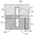
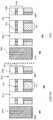
단일 핀을 이용하여 제작될 수 있는 회로 요소의 제1 예에서, 도 2a 및 2b는 본 발명의 한 실시예에 따른 단일 반도체 핀 구조물을 이용하여 제작된 인버터 회로 요소의 단면도를 나타낸다. 도 2a는 게이트 구조물을 통한 및 핀 구조물을 따른 단면도이다. 도 2b는 핀 구조물을 통한 및 게이트 구조물을 따른 단면도이다.In a first example of a circuit element that can be fabricated using a single fin, Figures 2a and 2b show cross-sectional views of an inverter circuit element fabricated using a single semiconductor fin structure in accordance with one embodiment of the present invention. Figure 2a is a cross-sectional view through the gate structure and along the pin structure. Figure 2b is a cross-sectional view through the fin structure and along the gate structure.
도 2a를 참조하면, 반도체 핀(202)은 상위 영역(202A)과 하위 영역(202B)으로 수직으로 분리된 것으로 볼 수 있다. 한 실시예에서, 반도체 핀(202)의 상위 영역(202A)과 하위 영역(202B)은 실리콘 산화물 층 또는 다른 절연 산화물 층 또는 실리콘 질화물 층 등의 절연 층(204)에 의해 분리된다. 절연 층(204)은, 구조물을 제작하는데 이용되는 집적 방식에 따라, 상이한 절연 재료의 영역들(204A 및 204B)을 포함할 수 있으며, 그 예가 이하에서 더 상세히 설명된다.Referring to FIG. 2A, the
PMOS 게이트 구조물 등의 제1 복수의 게이트 구조물(206)은 반도체 핀(202)의 상위 영역(202A) 위에 포함된다. 제1 복수의 게이트 구조물(206)들 각각은, 게이트 전극(208), 게이트 유전체 층(210) 및 연관된 유전체 스페이서(212)를 포함할 수 있다. 제1 복수의 게이트 구조물(206)은 (도시된) 반도체 핀(202)의 상위 영역(202A)의 상단으로부터 연장되고, 또한, 도 2a에 도시된 투시도에 관하여 페이지 속으로 들어가는 또는 페이지 바깥으로 나오는 위치들에서 반도체 핀(202)의 상위 영역(202A)을 감싼다는 것을 이해해야 한다. 반도체 핀(202)의 상위 영역(202A)은, 한 실시예에서, 재성장된 소스 또는 드레인 영역을 더 포함할 수 있다. 예시적인 실시예에서, 반도체 핀(202)의 상위 영역(202A)은 에피텍셜 P형 실리콘 게르마늄 영역(214)을 더 포함하고, 반도체 핀(202)의 상위 영역(202A)의 (실리콘 영역 등의) 나머지 반도체 영역(216)을 남긴다.A first plurality of
도 2a에는 도시되지 않고 도 2b에 도시되어 있지만, 반도체 핀(202)의 하위 영역(202B)은 NMOS 게이트 구조물 등의 제2 복수의 게이트 구조물(218)과 연관된다. 제2 복수의 게이트 구조물(218)들 각각은, 게이트 전극(220), 게이트 유전체 층(222) 및 연관된 유전체 스페이서를 포함할 수 있다. 제2 복수의 게이트 구조물(218)은 도 2a에 도시된 투시도에 관하여 페이지 속으로 들어가는 또는 페이지 바깥으로 나오는 위치들에서 반도체 핀(202)의 하위 영역(202B)을 감싸며, 따라서, 단지 도 2b의 단면도에서만, 즉, 영역(218A)에서만 볼 수 있다는 것을 이해해야 한다. 도 2b에 도시된 바와 같이, 반도체 구조물이 나노와이어 구조물인 특정한 실시예에서, 제2 복수의 게이트 구조물(218)들 각각은 또한, 위치(218B)들에서 반도체 핀(202)의 하위 영역(202B) 아래를 감싼다. 그러나, 또 다른 실시예에서, 벌크 핀 구조물이거나 그렇지 않으면 아래에 놓인 기판에 결합되는 핀 구조물의 경우, 제2 복수의 게이트 구조물(218)들 각각의 부분(218B)은 포함되지 않아, 트라이-게이트형 구조물이 형성된다.Although not shown in FIG. 2A and shown in FIG. 2B, the
도 2a를 다시 참조하면, 한 실시예에서, 반도체 핀(202)의 하위 영역(202B)은 재성장된 소스 또는 드레인 영역을 더 포함할 수 있다. 예시적인 실시예에서, 반도체 핀(202)의 하위 영역(202B)은 에피텍셜 N형 실리콘 영역(226)을 더 포함하고, 반도체 핀(202)의 하위 영역(202B)의 (실리콘 영역 등의) 나머지 반도체 영역(228)을 남긴다.Referring again to FIG. 2A, in one embodiment, the
한 실시예에서, 제1 복수의 게이트 구조물(206)들 각각은 제2 복수의 게이트 구조물(218)들 중 대응하는 것과 동일한 트렌치 내에 형성되지만, 제2 복수의 게이트 구조물(218)들 중 상기 대응하는 것 위에 수직으로 형성된다. 한 이러한 실시예에서, 제1 복수의 게이트 구조물(206)들 각각은, 도 2b에 도시된 바와 같이, 절연 층(224)에 의해 제2 복수의 게이트 구조물(218)들 중 대응하는 것으로부터 절연된다. 그러나, 또 다른 실시예에서, 제1 복수의 게이트 구조물(206)들 각각은 제2 복수의 게이트 구조물(218)들 중 대응하는 것과의 P/N 접합을 형성하여 소정의 게이트 쌍들을 효과적으로 함께 접속하거나 단락시킨다.In one embodiment, each of the first plurality of
다시 도 2a 및 도 2b를 참조하면, 한 실시예에서, 반도체 디바이스들의 층들 사이에 적층된 배선 및 배면 배선 등의 배선 고려사항은, 단일 핀의 디바이스들이 함께 회로 요소를 형성하도록 반드시 고려되어야 한다. 한 이러한 실시예에서, 제1 도전성 컨택트(230)는 제1 상위 영역(214) 및 제1 하위 영역(226)과 접촉하여 Vout 컨택트를 형성한다. 제2 도전성 컨택트(232)는 제2 상위 영역(214)과 접촉하여 Vcc 컨택트를 형성한다. 마지막으로, 제3 도전성 컨택트(234)는 제2 하위 영역(226)과 접촉하여 접지(GND)로의 컨택트를 형성한다.Referring again to Figures 2A and 2B, in one embodiment, wiring considerations such as stacked wiring and backside wiring between layers of semiconductor devices must be considered so that single pin devices form a circuit element together. In one such embodiment, the first
다시 도 2a 및 도 2b를 참조하면, 전체 인버터 구조물이 단일 핀(202) 상에 제작된다. 즉, 전체 회로 요소는 단일 반도체 핀 상에 제작된다. 이러한 인버터를 이용하여 SRAM 셀을 제작하기 위해, 2개의 이러한 인버터가 2개의 패스 게이트(pass gate)와 결합될 수 있다는 것을 이해해야 한다. 본 발명의 한 실시예에 따르면, 각각의 이러한 패스 게이트도 역시 단일 핀 상에 제작된다.Referring again to Figures 2a and 2b, the entire inverter structure is fabricated on a
단일 핀을 이용하여 제작될 수 있는 회로 요소의 제2 예에서, 도 3a 및 도 3b는 본 발명의 한 실시예에 따른 단일 반도체 핀 구조물을 이용하여 제작된 패스 게이트 회로 요소의 단면도를 나타낸다. 도 3a는 게이트 구조물을 통한 및 핀 구조물을 따른 단면도이다. 도 3b는 핀 구조물을 통한 및 게이트 구조물을 따른 단면도이다.In a second example of a circuit element that can be fabricated using a single fin, Figures 3a and 3b show cross-sectional views of passgate circuit elements fabricated using a single semiconductor fin structure in accordance with one embodiment of the present invention. Figure 3a is a cross-sectional view through the gate structure and along the fin structure. Figure 3b is a cross-sectional view through the fin structure and along the gate structure.
도 3a를 참조하면, 반도체 핀(302)은 상위 영역(302A)과 하위 영역(302B)으로 수직으로 분리된 것으로 볼 수 있다. 한 실시예에서, 반도체 핀(302)의 상위 영역(302A)과 하위 영역(302B)은 실리콘 산화물 층 또는 다른 절연 산화물 층 또는 실리콘 질화물 층 등의 절연 층(304)에 의해 분리된다. 절연 층(304)은, 구조물을 제작하는데 이용되는 집적 방식에 따라, 상이한 절연 재료의 영역들(304A 및 304B)을 포함할 수 있으며, 그 예가 이하에서 더 상세히 설명된다.Referring to FIG. 3A, the
NMOS 게이트 구조물 등의 제1 복수의 게이트 구조물(306)은 반도체 핀(302)의 상위 영역(302A) 위에 포함된다. 제1 복수의 게이트 구조물(306)들 각각은, 게이트 전극(308), 게이트 유전체 층(310) 및 연관된 유전체 스페이서(312)를 포함할 수 있다. 제1 복수의 게이트 구조물(306)은 (도시된) 반도체 핀(302)의 상위 영역(302A)의 상단으로부터 연장되고, 또한, 도 3a에 도시된 투시도에 관하여 페이지 속으로 들어가는 또는 페이지 바깥으로 나오는 위치들에서 반도체 핀(302)의 상위 영역(302A)을 감싼다는 것을 이해해야 한다. 반도체 핀(302)의 상위 영역(302A)은, 한 실시예에서, 재성장된 소스 또는 드레인 영역을 더 포함할 수 있다. 예시적인 실시예에서, 반도체 핀(302)의 상위 영역(302A)은 제1 에피텍셜 N형 실리콘 영역(314)을 더 포함하고, 반도체 핀(302)의 상위 영역(302A)의 (실리콘 영역 등의) 나머지 반도체 영역(316)을 남긴다.A first plurality of
도 3a에는 도시되지 않고 도 3b에 도시되어 있지만, 반도체 핀(302)의 하위 영역(302B)은 제2 복수의 NMOS 게이트 구조물 등의 제2 복수의 게이트 구조물(318)과 연관된다. 제2 복수의 게이트 구조물(318)들 각각은, 게이트 전극(320), 게이트 유전체 층(322) 및 연관된 유전체 스페이서를 포함할 수 있다. 제2 복수의 게이트 구조물(318)은 도 3a에 도시된 투시도에 관하여 페이지 속으로 들어가는 또는 페이지 바깥으로 나오는 위치들에서 반도체 핀(302)의 하위 영역(302B)을 감싸며, 따라서, 단지 도 3b의 단면도에서만, 즉, 영역(318A)에서만 볼 수 있다는 것을 이해해야 한다. 도 3b에 도시된 바와 같이, 반도체 구조물이 나노와이어 구조물인 특정한 실시예에서, 제2 복수의 게이트 구조물(318)들 각각은 또한, 위치(318B)들에서 반도체 핀(302)의 하위 영역(302B) 아래를 감싼다. 그러나, 또 다른 실시예에서, 벌크 핀 구조물이거나 그렇지 않으면 아래에 놓인 기판에 결합되는 핀 구조물의 경우, 제2 복수의 게이트 구조물(318)들 각각의 부분(318B)은 포함되지 않아, 트라이-게이트형 구조물이 형성된다.Although not shown in FIG. 3A, but shown in FIG. 3B, the
도 3a를 다시 참조하면, 한 실시예에서, 반도체 핀(302)의 하위 영역(302B)은 재성장된 소스 또는 드레인 영역을 더 포함할 수 있다. 예시적인 실시예에서, 반도체 핀(302)의 하위 영역(302B)은 에피텍셜 N형 실리콘 영역(326)을 더 포함하고, 반도체 핀(302)의 하위 영역(302B)의 (실리콘 영역 등의) 나머지 반도체 영역(328)을 남긴다.Referring again to FIG. 3A, in one embodiment, the
한 실시예에서, 제1 복수의 게이트 구조물(306)들 각각은 제2 복수의 게이트 구조물(318)들 중 대응하는 것과 동일한 트렌치 내에 형성되지만, 제2 복수의 게이트 구조물(318)들 중 상기 대응하는 것 위에 수직으로 형성된다. 한 이러한 실시예에서, 제1 복수의 게이트 구조물(306)들 각각은 동일한 도전형(예를 들어, N형)을 가지며, 도 3b에 도시된 바와 같이, 절연 층(324)에 의해 제2 복수의 게이트 구조물(318)들 중 대응하는 것으로부터 절연된다.In one embodiment, each of the first plurality of
다시 도 3a 및 도 3b를 참조하면, 한 실시예에서, 반도체 디바이스들의 층들 사이에 적층된 배선 및 배면 배선 등의 배선 고려사항은, 단일 핀의 디바이스들이 함께 회로 요소를 형성하도록 반드시 고려되어야 한다. 이러한 한 실시예에서, 제1 도전성 컨택트(330)는 제1 상위 영역(314)과 접촉하여 제1 인버터 요소로의 접속을 형성한다. 제2 도전성 컨택트(332)는 제1 하위 영역(326)과 접촉하여 제2 인버터 요소로의 접속을 형성한다. 제3 도전성 컨택트(334)는 제2 상위 영역(314)과 접촉하여 제1 비트라인 컨택트를 형성한다. 마지막으로, 제4 도전성 컨택트(336)는 제2 하위 영역(326)과 접촉하여 제2 비트라인 컨택트를 형성한다. 따라서, 전체 패스 게이트 구조물이 단일 핀(302) 상에 제작된다.Referring again to Figures 3a and 3b, in one embodiment, wiring considerations such as wiring and backside wiring stacked between layers of semiconductor devices must be considered so that single pin devices form a circuit element together. In one such embodiment, the first
현재의 솔루션은, 에칭/퇴적/및 리소그래피를 점점 더 작은 치수에서 수행하는데 있어서 공정 기술에 엄청난 제약을 가하는 폴리 피치 및 핀 피치의 감소를 수반한다는 것을 이해해야 한다. 대조적으로, 여기서 설명된 실시예들은 그려진 피치 스케일링없이 트랜지스터 밀도 증가를 허용한다. 실시예들은 AND 게이트(예를 들어, 도 4a 및 도 4b), OR 게이트(예를 들어, 도 5a 및 도 5b), NAND 아키텍쳐(예를 들어, 도 6a, 도 6b 및 도 7a 및 도 7b), NOR 아키텍쳐(예를 들어, 도 8a 내지 도 8d), 인버터(예를 들어, 도 2a 및 도 2b), SRAM 셀(예를 들어, 도 2a, 도 2b, 도 3a 및 도 3b) 및 기타의 랜덤 논리 컴포넌트들로의 이러한 접근법의 적용을 포함할 수 있다.It should be appreciated that current solutions involve a reduction in the poly pitch and fin pitch, which places significant constraints on process technology in performing etching / deposition / and lithography at increasingly smaller dimensions. In contrast, the embodiments described herein permit an increase in transistor density without drawn pitch scaling. (E.g., FIGS. 4A and 4B), an OR gate (e.g., FIGS. 5A and 5B), a NAND architecture (e.g., , A NOR architecture (e.g., FIGS. 8A-8D), an inverter (e.g., FIGS. 2A and 2B), an SRAM cell (e.g., FIGS. 2A, 2B, 3A, and 3B) And may include the application of this approach to random logic components.
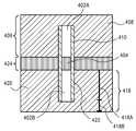
단일 핀을 이용하여 제작될 수 있는 회로 요소의 제3 예에서, 도 4a 및 도 4b는 본 발명의 한 실시예에 따른 단일 반도체 핀 구조물을 이용하여 제작된 AND 게이트 회로 요소의 단면도를 나타낸다. 도 4a는 게이트 구조물을 통한 및 핀 구조물을 따른 단면도이다. 도 4b는 핀 구조물을 통한 및 게이트 구조물을 따른 단면도이다.In a third example of a circuit element that may be fabricated using a single fin, FIGS. 4A and 4B show cross-sectional views of an AND gate circuit element fabricated using a single semiconductor fin structure in accordance with one embodiment of the present invention. 4A is a cross-sectional view through a gate structure and along a fin structure. Figure 4b is a cross-sectional view through the fin structure and along the gate structure.
도 4a를 참조하면, 반도체 핀(402)은 상위 영역(402A)과 하위 영역(402B)으로 수직으로 분리된 것으로 볼 수 있다. 한 실시예에서, 반도체 핀(402)의 상위 영역(402A)과 하위 영역(402B)은 실리콘 산화물 층 또는 다른 절연 산화물 층 또는 실리콘 질화물 층 등의 절연 층(404)에 의해 분리된다. 절연 층(404)은, 구조물을 제작하는데 이용되는 집적 방식에 따라, 상이한 절연 재료의 영역들(404A 및 404B)을 포함할 수 있으며, 그 예가 이하에서 더 상세히 설명된다.Referring to FIG. 4A, the
NMOS 게이트 구조물 등의 제1 복수의 게이트 구조물(406)은 반도체 핀(402)의 상위 영역(402A) 위에 포함된다. 제1 복수의 게이트 구조물(406)들 각각은, 게이트 전극(408), 게이트 유전체 층(410) 및 연관된 유전체 스페이서(412)를 포함할 수 있다. 제1 복수의 게이트 구조물(406)은 (도시된) 반도체 핀(402)의 상위 영역(402A)의 상단으로부터 연장되고, 또한, 도 4a에 도시된 투시도에 관하여 페이지 속으로 들어가는 또는 페이지 바깥으로 나오는 위치들에서 반도체 핀(402)의 상위 영역(402A)을 감싼다는 것을 이해해야 한다. 반도체 핀(402)의 상위 영역(402A)은, 한 실시예에서, 재성장된 소스 또는 드레인 영역을 더 포함할 수 있다. 예시적인 실시예에서, 반도체 핀(402)의 상위 영역(402A)은 제1 에피텍셜 N형 실리콘 영역(414)을 더 포함하고, 반도체 핀(402)의 상위 영역(402A)의 (실리콘 영역 등의) 나머지 반도체 영역(416)을 남긴다.A first plurality of
도 4a에는 도시되지 않고 도 4b에 도시되어 있지만, 반도체 핀(402)의 하위 영역(402B)은 제2 복수의 NMOS 게이트 구조물 등의 제2 복수의 게이트 구조물(418)과 연관된다. 제2 복수의 게이트 구조물(418)들 각각은, 게이트 전극(420), 게이트 유전체 층(422) 및 연관된 유전체 스페이서를 포함할 수 있다. 제2 복수의 게이트 구조물(418)은 도 4a에 도시된 투시도에 관하여 페이지 속으로 들어가는 또는 페이지 바깥으로 나오는 위치들에서 반도체 핀(402)의 하위 영역(402B)을 감싸며, 따라서, 단지 도 4b의 단면도에서만, 즉, 영역(418A)에서만 볼 수 있다는 것을 이해해야 한다. 도 4b에 도시된 바와 같이, 반도체 구조물이 나노와이어 구조물인 특정한 실시예에서, 제2 복수의 게이트 구조물(418)들 각각은 또한, 위치(418B)들에서 반도체 핀(402)의 하위 영역(402B) 아래를 감싼다. 그러나, 또 다른 실시예에서, 벌크 핀 구조물이거나 그렇지 않으면 아래에 놓인 기판에 결합되는 핀 구조물의 경우, 제2 복수의 게이트 구조물(418)들 각각의 부분(418B)은 포함되지 않아, 트라이-게이트형 구조물이 형성된다.Although not shown in FIG. 4A and shown in FIG. 4B, the
도 4a를 다시 참조하면, 한 실시예에서, 반도체 핀(402)의 하위 영역(402B)은 재성장된 소스 또는 드레인 영역을 더 포함할 수 있다. 예시적인 실시예에서, 반도체 핀(402)의 하위 영역(402B)은 에피텍셜 N형 실리콘 영역(426)을 더 포함하고, 반도체 핀(402)의 하위 영역(402B)의 (실리콘 영역 등의) 나머지 반도체 영역(428)을 남긴다.Referring again to FIG. 4A, in one embodiment, the
한 실시예에서, 제1 복수의 게이트 구조물(406)들 각각은 제2 복수의 게이트 구조물(418)들 중 대응하는 것과 동일한 트렌치 내에 형성되지만, 제2 복수의 게이트 구조물(418)들 중 상기 대응하는 것 위에 수직으로 형성된다. 한 이러한 실시예에서, 제1 복수의 게이트 구조물(406)들 각각은 동일한 도전형(예를 들어, N형)을 가지며, 도 4b에 도시된 바와 같이, 절연 층(424)에 의해 제2 복수의 게이트 구조물(418)들 중 대응하는 것으로부터 절연된다.In one embodiment, each of the first plurality of
다시 도 4a 및 도 4b를 참조하면, 한 실시예에서, 반도체 디바이스들의 층들 사이에 적층된 배선 및 배면 배선 등의 배선 고려사항은, 단일 핀의 디바이스들이 함께 회로 요소를 형성하도록 반드시 고려되어야 한다. 한 이러한 실시예에서, 제1 도전성 컨택트(430)는 제1 상위 영역(414) 및 제1 하위 영역(426)과 접촉하여 컨택트를 형성한다. 제2 도전성 컨택트(432)는 제2 상위 영역(414)과 접촉하여 OUT 단자를 형성한다. 마지막으로, 제3 도전성 컨택트(434)는 제2 하위 영역(426)과 접촉하여 접지(GND)로의 컨택트를 형성한다. 따라서, 전체 AND 게이트 구조물이 단일 핀(402) 상에 제작된다.Referring again to Figures 4A and 4B, in one embodiment, wiring considerations such as wiring and backside wiring stacked between layers of semiconductor devices must be considered so that single pin devices form a circuit element together. In one such embodiment, the first
단일 핀을 이용하여 제작될 수 있는 회로 요소의 제4 예에서, 도 5a 및 도 5b는 본 발명의 한 실시예에 따른 단일 반도체 핀 구조물을 이용하여 제작된 OR 게이트 회로 요소의 단면도를 나타낸다. 도 5a는 게이트 구조물을 통한 및 핀 구조물을 따른 단면도이다. 도 5b는 핀 구조물을 통한 및 게이트 구조물을 따른 단면도이다.In a fourth example of a circuit element that may be fabricated using a single fin, Figures 5A and 5B show cross-sectional views of OR gate circuit elements fabricated using a single semiconductor fin structure in accordance with one embodiment of the present invention. 5A is a cross-sectional view through a gate structure and along a fin structure. Figure 5b is a cross-sectional view through the fin structure and along the gate structure.
도 5a를 참조하면, 반도체 핀(502)은 상위 영역(502A)과 하위 영역(502B)으로 수직으로 분리된 것으로 볼 수 있다. 한 실시예에서, 반도체 핀(502)의 상위 영역(502A)과 하위 영역(502B)은 실리콘 산화물 층 또는 다른 절연 산화물 층 또는 실리콘 질화물 층 등의 절연 층(504)에 의해 분리된다. 절연 층(504)은, 구조물을 제작하는데 이용되는 집적 방식에 따라, 상이한 절연 재료의 영역들(504A 및 504B)을 포함할 수 있으며, 그 예가 이하에서 더 상세히 설명된다.Referring to FIG. 5A, the
NMOS 게이트 구조물 등의 제1 복수의 게이트 구조물(506)은 반도체 핀(502)의 상위 영역(502A) 위에 포함된다. 제1 복수의 게이트 구조물(506)들 각각은, 게이트 전극(508), 게이트 유전체 층(510) 및 연관된 유전체 스페이서(512)를 포함할 수 있다. 제1 복수의 게이트 구조물(506)은 (도시된) 반도체 핀(502)의 상위 영역(502A)의 상단으로부터 연장되고, 또한, 도 5a에 도시된 투시도에 관하여 페이지 속으로 들어가는 또는 페이지 바깥으로 나오는 위치들에서 반도체 핀(502)의 상위 영역(502A)을 감싼다는 것을 이해해야 한다. 반도체 핀(502)의 상위 영역(502A)은, 한 실시예에서, 재성장된 소스 또는 드레인 영역을 더 포함할 수 있다. 예시적인 실시예에서, 반도체 핀(502)의 상위 영역(502A)은 제1 에피텍셜 N형 실리콘 영역(514)을 더 포함하고, 반도체 핀(502)의 상위 영역(502A)의 (실리콘 영역 등의) 나머지 반도체 영역(516)을 남긴다.A first plurality of
도 5a에는 도시되지 않고 도 5b에 도시되어 있지만, 반도체 핀(502)의 하위 영역(502B)은 제2 복수의 NMOS 게이트 구조물 등의 제2 복수의 게이트 구조물(518)과 연관된다. 제2 복수의 게이트 구조물(518)들 각각은, 게이트 전극(520), 게이트 유전체 층(522) 및 연관된 유전체 스페이서를 포함할 수 있다. 제2 복수의 게이트 구조물(518)은 도 5a에 도시된 투시도에 관하여 페이지 속으로 들어가는 또는 페이지 바깥으로 나오는 위치들에서 반도체 핀(502)의 하위 영역(502B)을 감싸며, 따라서, 단지 도 5b의 단면도에서만, 즉, 영역(518A)에서만 볼 수 있다는 것을 이해해야 한다. 도 5b에 도시된 바와 같이, 반도체 구조물이 나노와이어 구조물인 특정한 실시예에서, 제2 복수의 게이트 구조물(518)들 각각은 또한, 위치(518B)들에서 반도체 핀(502)의 하위 영역(502B) 아래를 감싼다. 그러나, 또 다른 실시예에서, 벌크 핀 구조물이거나 그렇지 않으면 아래에 놓인 기판에 결합되는 핀 구조물의 경우, 제2 복수의 게이트 구조물(518)들 각각의 부분(518B)은 포함되지 않아, 트라이-게이트형 구조물이 형성된다.5B, the
도 5a를 다시 참조하면, 한 실시예에서, 반도체 핀(502)의 하위 영역(502B)은 재성장된 소스 또는 드레인 영역을 더 포함할 수 있다. 예시적인 실시예에서, 반도체 핀(502)의 하위 영역(502B)은 에피텍셜 N형 실리콘 영역(526)을 더 포함하고, 반도체 핀(502)의 하위 영역(502B)의 (실리콘 영역 등의) 나머지 반도체 영역(528)을 남긴다.Referring again to FIG. 5A, in one embodiment, the
한 실시예에서, 제1 복수의 게이트 구조물(506)들 각각은 제2 복수의 게이트 구조물(518)들 중 대응하는 것과 동일한 트렌치 내에 형성되지만, 제2 복수의 게이트 구조물(518)들 중 상기 대응하는 것 위에 수직으로 형성된다. 한 이러한 실시예에서, 제1 복수의 게이트 구조물(506)들 각각은 동일한 도전형(예를 들어, N형)을 가지며, 도 5b에 도시된 바와 같이, 절연 층(524)에 의해 제2 복수의 게이트 구조물(518)들 중 대응하는 것으로부터 절연된다.In one embodiment, each of the first plurality of
다시 도 5a 및 도 5b를 참조하면, 한 실시예에서, 반도체 디바이스들의 층들 사이에 적층된 배선 및 배면 배선 등의 배선 고려사항은, 단일 핀의 디바이스들이 함께 회로 요소를 형성하도록 반드시 고려되어야 한다. 한 이러한 실시예에서, 제1 도전성 컨택트(530)는 제1 상위 영역(514) 및 제1 하위 영역(526)과 접촉한다. 제2 도전성 컨택트(532)는 제2 상위 영역(514) 및 제2 하위 영역(526)과 접촉한다. 따라서, 전체 OR 게이트 구조물이 단일 핀(502) 상에 제작된다.Referring again to Figures 5A and 5B, in one embodiment, wiring considerations such as wiring and backside wiring stacked between layers of semiconductor devices must be considered so that single pin devices form a circuit element together. In one such embodiment, the first
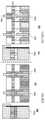
NAND 게이트 아키텍쳐는, 후술되는 바와 같이, 2개의 직렬 NMOS(예를 들어, 도 7a 및 7b)에 접속된 출력 노드를 갖는 2개의 병렬 PMOS(예를 들어, 도 6a 및 6b)로 분할될 수 있다.The NAND gate architecture can be divided into two parallel PMOSs (e.g., FIGS. 6A and 6B) having output nodes connected to two serial NMOSs (e.g., FIGS. 7A and 7B), as described below .
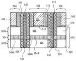
단일 핀을 이용하여 제작될 수 있는 회로 요소의 제5 예에서, 도 6a 및 도 6b는 본 발명의 한 실시예에 따른 NAND 게이트 회로 요소의 컴포넌트로서 단일 반도체 핀 구조물을 이용하여 제작된 2개의 병렬 PMOS 디바이스에 기초한 회로 요소의 단면도를 나타낸다. 도 6a는 게이트 구조물을 통한 및 핀 구조물을 따른 단면도이다. 도 6b는 핀 구조물을 통한 및 게이트 구조물을 따른 단면도이다.In a fifth example of a circuit element that can be fabricated using a single fin, FIGS. 6A and 6B illustrate two parallel structures fabricated using a single semiconductor fin structure as a component of a NAND gate circuit element in accordance with an embodiment of the present invention. Lt; RTI ID = 0.0 > PMOS < / RTI > device. 6A is a cross-sectional view through the gate structure and along the fin structure. 6B is a cross-sectional view through the fin structure and along the gate structure.
도 6a를 참조하면, 반도체 핀(602)은 상위 영역(602A)과 하위 영역(602B)으로 수직으로 분리된 것으로 볼 수 있다. 한 실시예에서, 반도체 핀(602)의 상위 영역(602A)과 하위 영역(602B)은 실리콘 산화물 층 또는 다른 절연 산화물 층 또는 실리콘 질화물 층 등의 절연 층(604)에 의해 분리된다. 반도체 핀(602)은 또한, 도 6a에 도시된 바와 같이, 산화물 층 등의, 절연 층(603) 상에 배치될 수 있다.Referring to FIG. 6A, the
제1 복수의 PMOS 게이트 구조물(606)은 반도체 핀(602)의 상위 영역(602A) 위에 포함된다. 제1 복수의 PMOS 게이트 구조물(606)들 각각은, 게이트 전극(608), 게이트 유전체 층(610) 및 연관된 유전체 스페이서(612)를 포함할 수 있다. 제1 복수의 PMOS 게이트 구조물(606)은 (도시된) 반도체 핀(602)의 상위 영역(602A)의 상단으로부터 연장되고, 또한, 도 6a에 도시된 투시도에 관하여 페이지 속으로 들어가는 또는 페이지 바깥으로 나오는 위치들에서 반도체 핀(602)의 상위 영역(602A)을 감싼다는 것을 이해해야 한다.A first plurality of
도 6a에는 도시되지 않고 도 6b에 도시되어 있지만, 반도체 핀(602)의 하위 영역(602B)은 제2 복수의 PMOS 게이트 구조물(618)과 연관된다. 제2 복수의 PMOS 게이트 구조물(618)들 각각은, 게이트 전극(620), 게이트 유전체 층(622) 및 연관된 유전체 스페이서를 포함할 수 있다. 제2 복수의 PMOS 게이트 구조물(618)은 도 6a에 도시된 투시도에 관하여 페이지 속으로 들어가는 또는 페이지 바깥으로 나오는 위치들에서 반도체 핀(602)의 하위 영역(602B)을 감싸며, 따라서, 단지 도 6b의 단면도에서만, 즉, 영역(618A)에서만 볼 수 있다는 것을 이해해야 한다. 도 6b에 도시된 바와 같이, 반도체 구조물이 나노와이어 구조물인 특정한 실시예에서, 제2 복수의 PMOS 게이트 구조물(618)들 각각은 또한, 위치(618B)들에서 반도체 핀(602)의 하위 영역(602B) 아래를 감싼다. 그러나, 또 다른 실시예에서, 벌크 핀 구조물이거나 그렇지 않으면 아래에 놓인 기판 또는 산화물 층(603)에 결합되는 핀 구조물의 경우, 제2 복수의 PMOS 게이트 구조물(618)들 각각의 부분(618B)은 포함되지 않아, 트라이-게이트형 구조물이 형성된다.Although not shown in FIG. 6A and shown in FIG. 6B, the
도 6a를 다시 참조하면, 한 실시예에서, 반도체 핀(602)의 상위 영역(602A)과 하위 영역(602B) 양쪽 모두는 재성장된 소스 또는 드레인 영역을 더 포함할 수 있다. 예시적인 실시예에서, 반도체 핀(602)의 상위 영역(602A)과 하위 영역(602B) 양쪽 모두는 에피텍셜 P형 실리콘 게르마늄 영역(626)을 더 포함하고, 반도체 핀(602)의 (실리콘 영역 등의) 나머지 반도체 영역(628)을 남긴다.Referring again to FIG. 6A, in one embodiment, both the
한 실시예에서, 제1 복수의 PMOS 게이트 구조물(606)들 각각은 제2 복수의 PMOS 게이트 구조물(618)들 중 대응하는 것과 동일한 트렌치 내에 형성되지만, 제2 복수의 PMOS 게이트 구조물(618)들 중 상기 대응하는 것 위에 수직으로 형성된다. 한 이러한 실시예에서, 제1 복수의 PMOS 게이트 구조물(606)들 각각은, 도 6b에 도시된 바와 같이, 절연 층(624)에 의해 제2 복수의 PMOS 게이트 구조물(618)들 중 대응하는 것으로부터 절연된다.In one embodiment, each of the first plurality of
다시 도 6a 및 도 6b를 참조하면, 한 실시예에서, 반도체 디바이스들의 층들 사이에 적층된 배선 및 배면 배선 등의 배선 고려사항은, 단일 핀의 디바이스들이 함께 회로 요소를 형성하도록 반드시 고려되어야 한다. 한 이러한 실시예에서, 제1 도전성 컨택트(630)는 제1 에피텍셜 P형 실리콘 게르마늄 영역(626)과 접촉하여 Vcc 컨택트를 형성한다. 제2 도전성 컨택트(632)는 제2 에피텍셜 P형 실리콘 게르마늄 영역(626)과 접촉하여 Vout 컨택트를 형성한다.Referring again to Figures 6a and 6b, in one embodiment, wiring considerations such as wiring and backside wiring stacked between layers of semiconductor devices must be considered so that single pin devices form a circuit element together. In one such embodiment, the first
단일 핀을 이용하여 제작될 수 있는 회로 요소의 제6 예에서, 도 7a 및 도 7b는 본 발명의 한 실시예에 따른 도 6a 및 도 6b의 2개의 병렬 PMOS 디바이스와 결합하기 위한 NAND 게이트 회로 요소의 컴포넌트로서 단일 반도체 핀 구조물을 이용하여 제작된 2개의 직렬 NMOS 디바이스에 기초한 회로 요소의 단면도를 나타낸다. 도 7a는 게이트 구조물을 통한 및 핀 구조물을 따른 단면도이다. 도 7b는 핀 구조물을 통한 및 게이트 구조물을 따른 단면도이다.In a sixth example of a circuit element that may be fabricated using a single fin, FIGS. 7A and 7B illustrate a NAND gate circuit element for coupling with two parallel PMOS devices of FIGS. 6A and 6B, according to one embodiment of the present invention. Lt; / RTI > shows a cross-sectional view of a circuit element based on two series NMOS devices fabricated using a single semiconductor fin structure as a component of the device. 7A is a cross-sectional view through the gate structure and along the fin structure. Figure 7b is a cross-sectional view through the fin structure and along the gate structure.
도 7a를 참조하면, 반도체 핀(702)은 상위 영역(702A)과 하위 영역(702B)으로 수직으로 분리된 것으로 볼 수 있다. 한 실시예에서, 반도체 핀(702)의 상위 영역(702A)과 하위 영역(702B)은 실리콘 산화물 층 또는 다른 절연 산화물 층 또는 실리콘 질화물 층 등의 절연 층(704)에 의해 분리된다. 반도체 핀(702)은 또한, 도 7a에 도시된 바와 같이, 산화물 층 등의, 절연 층(703) 상에 배치될 수 있다.Referring to FIG. 7A, the semiconductor fin 702 may be seen as vertically separated into an
제1 복수의 NMOS 게이트 구조물(706)은 반도체 핀(702)의 상위 영역(702A) 위에 포함된다. 제1 복수의 NMOS 게이트 구조물(706)들 각각은, 게이트 전극(708), 게이트 유전체 층(710) 및 연관된 유전체 스페이서(712)를 포함할 수 있다. 제1 복수의 NMOS 게이트 구조물(706)은 (도시된) 반도체 핀(702)의 상위 영역(702A)의 상단으로부터 연장되고, 또한, 도 7a에 도시된 투시도에 관하여 페이지 속으로 들어가는 또는 페이지 바깥으로 나오는 위치들에서 반도체 핀(702)의 상위 영역(702A)을 감싼다는 것을 이해해야 한다.A first plurality of
도 7a에는 도시되지 않고 도 7b에 도시되어 있지만, 반도체 핀(702)의 하위 영역(702B)은 제2 복수의 NMOS 게이트 구조물(718)과 연관된다. 제2 복수의 NMOS 게이트 구조물(718)들 각각은, 게이트 전극(720), 게이트 유전체 층(722) 및 연관된 유전체 스페이서를 포함할 수 있다. 제2 복수의 NMOS 게이트 구조물(718)은 도 7a에 도시된 투시도에 관하여 페이지 속으로 들어가는 또는 페이지 바깥으로 나오는 위치들에서 반도체 핀(702)의 하위 영역(702B)을 감싸며, 따라서, 단지 도 7b의 단면도에서만, 즉, 영역(718A)에서만 볼 수 있다는 것을 이해해야 한다. 도 7b에 도시된 바와 같이, 반도체 구조물이 나노와이어 구조물인 특정한 실시예에서, 제2 복수의 NMOS 게이트 구조물(718)들 각각은 또한, 위치(718B)들에서 반도체 핀(702)의 하위 영역(702B) 아래를 감싼다. 그러나, 또 다른 실시예에서, 벌크 핀 구조물이거나 그렇지 않으면 아래에 놓인 기판 또는 산화물 층(703)에 결합되는 핀 구조물의 경우, 제2 복수의 NMOS 게이트 구조물(718)들 각각의 부분(718B)은 포함되지 않아, 트라이-게이트형 구조물이 형성된다.Although not shown in FIG. 7A and shown in FIG. 7B, the
도 7a를 다시 참조하면, 한 실시예에서, 반도체 핀(702)의 상위 영역(702A)과 하위 영역(702B) 양쪽 모두는 재성장된 소스 또는 드레인 영역을 더 포함할 수 있다. 예시적인 실시예에서, 반도체 핀(702)의 상위 영역(702A)과 하위 영역(702B) 양쪽 모두는 에피텍셜 N형 실리콘 영역(726)을 더 포함하고, 반도체 핀(702)의 (실리콘 영역 등의) 나머지 반도체 영역(728)을 남긴다. 또한, 상위 에피텍셜 N형 실리콘 영역(727A)은 반도체 핀(702)의 상위 영역(702A)에만 형성되는 반면, 하위 에피텍셜 N형 실리콘 영역(727B)은 반도체 핀(702)의 하위 영역(702B)에만 형성된다. 절연 층 부분(704B)은 상위 에피텍셜 N형 실리콘 영역(727A)을 하위 에피텍셜 N형 실리콘 영역(727B)으로부터 분리한다.Referring again to FIG. 7A, in one embodiment, both the
한 실시예에서, 제1 복수의 NMOS 게이트 구조물(706)들 각각은 제2 복수의 NMOS 게이트 구조물(718)들 중 대응하는 것과 동일한 트렌치 내에 형성되지만, 제2 복수의 NMOS 게이트 구조물(718)들 중 상기 대응하는 것 위에 수직으로 형성된다. 한 이러한 실시예에서, 제1 복수의 NMOS 게이트 구조물(706)들 각각은, 도 7b에 도시된 바와 같이, 절연 층(724)에 의해 제2 복수의 NMOS 게이트 구조물(718)들 중 대응하는 것으로부터 절연된다.In one embodiment, each of the first plurality of
다시 도 7a 및 도 7b를 참조하면, 한 실시예에서, 반도체 디바이스들의 층들 사이에 적층된 배선 및 배면 배선 등의 배선 고려사항은, 단일 핀의 디바이스들이 함께 회로 요소를 형성하도록 반드시 고려되어야 한다. 한 이러한 실시예에서, 제1 도전성 컨택트(730)는 에피텍셜 N형 실리콘 영역(726)과 접촉한다. 제2 도전성 컨택트(732)는 하위 에피텍셜 N형 실리콘 영역(727B)과 접촉하여 Vout 컨택트를 형성한다. 제3 도전성 컨택트(734)는 상위 에피텍셜 N형 실리콘 영역(727A)과 접촉하여 접지(GND)로의 컨택트를 형성한다.Referring again to Figures 7a and 7b, in one embodiment, wiring considerations such as wiring and backside wiring stacked between layers of semiconductor devices must be considered so that single pin devices form a circuit element together. In one such embodiment, the first
NAND 아키텍쳐와 유사한 방식으로, NOR 게이트 아키텍쳐는, 이하에서 설명되는 바와 같이, 그 출력이 2개의 직렬 PMOS(예를 들어, 도 8c 및 8d)의 출력에 접속되는, 2개의 병렬 NMOS(예를 들어, 도 8a 및 도 8b)로 분할될 수 있다.In a manner similar to the NAND architecture, the NOR gate architecture may be implemented using two parallel NMOSs (e.g., two parallel NMOSs) whose outputs are connected to the outputs of two serial PMOSs (e.g., , Figs. 8A and 8B).
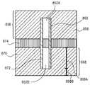
단일 핀을 이용하여 제작될 수 있는 회로 요소의 제7 예에서, 도 8a 및 도 8b는 본 발명의 한 실시예에 따른 NOR 게이트 회로 요소의 컴포넌트로서 단일 반도체 핀 구조물을 이용하여 제작된 2개의 병렬 NMOS 디바이스에 기초한 회로 요소의 단면도를 나타낸다. 도 8a는 게이트 구조물을 통한 및 핀 구조물을 따른 단면도이다. 도 8b는 핀 구조물을 통한 및 게이트 구조물을 따른 단면도이다.In a seventh example of a circuit element that can be fabricated using a single fin, FIGS. 8A and 8B illustrate two parallel structures fabricated using a single semiconductor fin structure as a component of a NOR gate circuit element in accordance with an embodiment of the present invention. Lt; / RTI > shows a cross-sectional view of a circuit element based on an NMOS device. 8A is a cross-sectional view through a gate structure and along a fin structure. Figure 8b is a cross-sectional view through the fin structure and along the gate structure.
도 8a를 참조하면, 반도체 핀(802)은 상위 영역(802A)과 하위 영역(802B)으로 수직으로 분리된 것으로 볼 수 있다. 한 실시예에서, 반도체 핀(802)의 상위 영역(802A)과 하위 영역(802B)은 실리콘 산화물 층 또는 다른 절연 산화물 층 또는 실리콘 질화물 층 등의 절연 층(804)에 의해 분리된다. 반도체 핀(802)은 또한, 도 8a에 도시된 바와 같이, 산화물 층 등의, 절연 층(803) 상에 배치될 수 있다.Referring to FIG. 8A, the
제1 복수의 NMOS 게이트 구조물(806)은 반도체 핀(802)의 상위 영역(802A) 위에 포함된다. 제1 복수의 NMOS 게이트 구조물(806)들 각각은, 게이트 전극(808), 게이트 유전체 층(810) 및 연관된 유전체 스페이서(812)를 포함할 수 있다. 제1 복수의 NMOS 게이트 구조물(806)은 (도시된) 반도체 핀(802)의 상위 영역(802A)의 상단으로부터 연장되고, 또한, 도 8a에 도시된 투시도에 관하여 페이지 속으로 들어가는 또는 페이지 바깥으로 나오는 위치들에서 반도체 핀(802)의 상위 영역(802A)을 감싼다는 것을 이해해야 한다.A first plurality of
도 8a에는 도시되지 않고 도 8b에 도시되어 있지만, 반도체 핀(802)의 하위 영역(802B)은 제2 복수의 NMOS 게이트 구조물(818)과 연관된다. 제2 복수의 NMOS 게이트 구조물(818)들 각각은, 게이트 전극(820), 게이트 유전체 층(822) 및 연관된 유전체 스페이서를 포함할 수 있다. 제2 복수의 NMOS 게이트 구조물(818)은 도 8a에 도시된 투시도에 관하여 페이지 속으로 들어가는 또는 페이지 바깥으로 나오는 위치들에서 반도체 핀(802)의 하위 영역(802B)을 감싸며, 따라서, 단지 도 8b의 단면도에서만, 즉, 영역(818A)에서만 볼 수 있다는 것을 이해해야 한다. 도 8b에 도시된 바와 같이, 반도체 구조물이 나노와이어 구조물인 특정한 실시예에서, 제2 복수의 NMOS 게이트 구조물(818)들 각각은 또한, 위치(818B)들에서 반도체 핀(802)의 하위 영역(802B) 아래를 감싼다. 그러나, 또 다른 실시예에서, 벌크 핀 구조물이거나 그렇지 않으면 아래에 놓인 기판 또는 산화물 층(803)에 결합되는 핀 구조물의 경우, 제2 복수의 NMOS 게이트 구조물(818)들 각각의 부분(818B)은 포함되지 않아, 트라이-게이트형 구조물이 형성된다.Although not shown in FIG. 8A and shown in FIG. 8B, the
도 8a를 다시 참조하면, 한 실시예에서, 반도체 핀(802)의 상위 영역(802A)과 하위 영역(802B) 양쪽 모두는 재성장된 소스 또는 드레인 영역을 더 포함할 수 있다. 예시적인 실시예에서, 반도체 핀(802)의 상위 영역(802A)과 하위 영역(802B) 양쪽 모두는 에피텍셜 N형 실리콘 영역(826)을 더 포함하고, 반도체 핀(802)의 (실리콘 영역 등의) 나머지 반도체 영역(828)을 남긴다.Referring again to Fig. 8A, in one embodiment, both the
한 실시예에서, 제1 복수의 NMOS 게이트 구조물(806)들 각각은 제2 복수의 NMOS 게이트 구조물(818)들 중 대응하는 것과 동일한 트렌치 내에 형성되지만, 제2 복수의 NMOS 게이트 구조물(818)들 중 상기 대응하는 것 위에 수직으로 형성된다. 한 이러한 실시예에서, 제1 복수의 NMOS 게이트 구조물(806)들 각각은, 도 8b에 도시된 바와 같이, 절연 층(824)에 의해 제2 복수의 NMOS 게이트 구조물(818)들 중 대응하는 것으로부터 절연된다.In one embodiment, each of the first plurality of
다시 도 8a 및 도 8b를 참조하면, 한 실시예에서, 반도체 디바이스들의 층들 사이에 적층된 배선 및 배면 배선 등의 배선 고려사항은, 단일 핀의 디바이스들이 함께 회로 요소를 형성하도록 반드시 고려되어야 한다. 한 이러한 실시예에서, 제1 도전성 컨택트(830)는 제1 에피텍셜 N형 실리콘 영역(826)과 접촉하여 접지(GND) 컨택트를 형성한다. 제2 도전성 컨택트(832)는 제2 에피텍셜 N형 실리콘 영역(826)과 접촉하여 Vout 컨택트를 형성한다. 전력을 전달하는 방법에 따라, 컨택트는 디바이스의 상부로부터 또는 하부로부터 이루어질 수 있다는 것을 이해해야 한다.Referring again to Figures 8A and 8B, in one embodiment, wiring considerations such as wiring and backside wiring stacked between layers of semiconductor devices must be considered so that the single pin devices together form a circuit element. In one such embodiment, the first
단일 핀을 이용하여 제작될 수 있는 회로 요소의 제8 예에서, 도 8c 및 도 8d는 본 발명의 한 실시예에 따른 도 8a 및 도 8b의 2개의 병렬 NMOS 디바이스와 결합하기 위한 NOR 게이트 회로 요소의 컴포넌트로서 단일 반도체 핀 구조물을 이용하여 제작된 2개의 직렬 PMOS 디바이스에 기초한 회로 요소의 단면도를 나타낸다. 도 8c는 게이트 구조물을 통한 및 핀 구조물을 따른 단면도이다. 도 8d는 핀 구조물을 통한 및 게이트 구조물을 따른 단면도이다.In an eighth example of a circuit element that can be fabricated using a single pin, FIGS. 8C and 8D illustrate a NOR gate circuit element for coupling with two parallel NMOS devices of FIGS. 8A and 8B, according to one embodiment of the present invention. Lt; / RTI > shows a cross-sectional view of a circuit element based on two series PMOS devices fabricated using a single semiconductor fin structure. 8C is a cross-sectional view through the gate structure and along the fin structure. 8D is a cross-sectional view through the fin structure and along the gate structure.
도 8c를 참조하면, 반도체 핀(852)은 상위 영역(852A)과 하위 영역(852B)으로 수직으로 분리된 것으로 볼 수 있다. 한 실시예에서, 반도체 핀(852)의 상위 영역(852A)과 하위 영역(852B)은 실리콘 산화물 층 또는 다른 절연 산화물 층 또는 실리콘 질화물 층 등의 절연 층(854)에 의해 분리된다. 반도체 핀(852)은 또한, 도 8c에 도시된 바와 같이, 산화물 층 등의, 절연 층(853) 상에 배치될 수 있다.Referring to FIG. 8C, the semiconductor pin 852 may be seen as vertically separated into an
제1 복수의 PMOS 게이트 구조물(856)은 반도체 핀(852)의 상위 영역(852A) 위에 포함된다. 제1 복수의 PMOS 게이트 구조물(856)들 각각은, 게이트 전극(858), 게이트 유전체 층(860) 및 연관된 유전체 스페이서(862)를 포함할 수 있다. 제1 복수의 PMOS 게이트 구조물(856)은 (도시된) 반도체 핀(852)의 상위 영역(852A)의 상단으로부터 연장되고, 또한, 도 8c에 도시된 투시도에 관하여 페이지 속으로 들어가는 또는 페이지 바깥으로 나오는 위치들에서 반도체 핀(852)의 상위 영역(852A)을 감싼다는 것을 이해해야 한다.A first plurality of
도 8c에는 도시되지 않고 도 8d에 도시되어 있지만, 반도체 핀(852)의 하위 영역(852B)은 제2 복수의 PMOS 게이트 구조물(868)과 연관된다. 제2 복수의 PMOS 게이트 구조물(868)들 각각은, 게이트 전극(870), 게이트 유전체 층(872) 및 연관된 유전체 스페이서를 포함할 수 있다. 제2 복수의 PMOS 게이트 구조물(868)은 도 8c에 도시된 투시도에 관하여 페이지 속으로 들어가는 또는 페이지 바깥으로 나오는 위치들에서 반도체 핀(852)의 하위 영역(852B)을 감싸며, 따라서, 단지 도 8d의 단면도에서만, 즉, 영역(868A)에서만 볼 수 있다는 것을 이해해야 한다. 도 8d에 도시된 바와 같이, 반도체 구조물이 나노와이어 구조물인 특정한 실시예에서, 제2 복수의 PMOS 게이트 구조물(868)들 각각은 또한, 위치(868B)들에서 반도체 핀(852)의 하위 영역(852B) 아래를 감싼다. 그러나, 또 다른 실시예에서, 벌크 핀 구조물이거나 그렇지 않으면 아래에 놓인 기판 또는 산화물 층(853)에 결합되는 핀 구조물의 경우, 제2 복수의 PMOS 게이트 구조물(868)들 각각의 부분(868B)은 포함되지 않아, 트라이-게이트형 구조물이 형성된다.Although not shown in FIG. 8C and shown in FIG. 8D, the
도 8c를 다시 참조하면, 한 실시예에서, 반도체 핀(852)의 상위 영역(852A)과 하위 영역(852B) 양쪽 모두는 재성장된 소스 또는 드레인 영역을 더 포함할 수 있다. 예시적인 실시예에서, 반도체 핀(852)의 상위 영역(852A)과 하위 영역(852B) 양쪽 모두는 에피텍셜 P형 실리콘 게르마늄 영역(876)을 더 포함하고, 반도체 핀(852)의 (실리콘 영역 등의) 나머지 반도체 영역(878)을 남긴다. 또한, 상위 에피텍셜 P형 실리콘 게르마늄 영역(877A)은 반도체 핀(852)의 상위 영역(852A)에만 형성되는 반면, 하위 에피텍셜 P형 실리콘 게르마늄 영역(877B)은 반도체 핀(852)의 하위 영역(852B)에만 형성된다. 절연 층 부분(854B)은 상위 에피텍셜 P형 실리콘 게르마늄 영역(877A)을 하위 에피텍셜 P형 실리콘 게르마늄 영역(877B)으로부터 분리한다.Referring again to FIG. 8C, in one embodiment, both the
한 실시예에서, 제1 복수의 PMOS 게이트 구조물(856)들 각각은 제2 복수의 PMOS 게이트 구조물(868)들 중 대응하는 것과 동일한 트렌치 내에 형성되지만, 제2 복수의 PMOS 게이트 구조물(868)들 중 상기 대응하는 것 위에 수직으로 형성된다. 한 이러한 실시예에서, 제1 복수의 PMOS 게이트 구조물(856)들 각각은, 도 8d에 도시된 바와 같이, 절연 층(874)에 의해 제2 복수의 PMOS 게이트 구조물(868)들 중 대응하는 것으로부터 절연된다.In one embodiment, each of the first plurality of
다시 도 8c 및 도 8d를 참조하면, 한 실시예에서, 반도체 디바이스들의 층들 사이에 적층된 배선 및 배면 배선 등의 배선 고려사항은, 단일 핀의 디바이스들이 함께 회로 요소를 형성하도록 반드시 고려되어야 한다. 한 이러한 실시예에서, 제1 도전성 컨택트(880)는 에피텍셜 P형 실리콘 게르마늄 영역(876)과 접촉한다. 제2 도전성 컨택트(882)는 하위 에피텍셜 P형 실리콘 게르마늄 영역(877B)과 접촉하여 Vcc 컨택트를 형성한다. 제3 도전성 컨택트(884)는 상위 에피텍셜 P형 실리콘 게르마늄 영역(877A)과 접촉하여 Vout 컨택트를 형성한다. 전력을 전달하는 방법에 따라, 컨택트는 디바이스의 상부로부터 또는 하부로부터 이루어질 수 있다는 것을 이해해야 한다.Referring again to Figures 8c and 8d, in one embodiment, wiring considerations such as stacked wiring and backside wiring between layers of semiconductor devices must be considered so that single pin devices form a circuit element together. In one such embodiment, the first
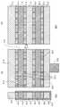
또 다른 양태에서, 대응하는 핀당 단일 트랜지스터 대신에 회로 요소들을 제조하기 위해, 한 실시예에서, 각각의 핀에 대한 2개의 트랜지스터의 절연이 요구된다. 그 다음, 팁(tip) 및 소스/드레인 영역은 하단 트랜지스터에서 정의될 수 있고 하단 트랜지스터에서의 컨택트 형성이 후속된다. 후속해서, 상단 트랜지스터로부터의 하단 트랜지스터의 절연이 수행된다. 그 다음, 팁 및 소스/드레인 영역이 상단 트랜지스터에 대해 형성된다. 후속해서, 하단 및 상단 트랜지스터 양쪽 모두에 대해 금속 게이트가 제작되고, 상단 트랜지스터로의 컨택트가 형성된다. 상단 트랜지스터에 대한 컨택트 형성도 역시 상단 및 하단 트랜지스터를 위한 금속 게이트를 형성한 후에 수행될 수 있다. 예시적인 실시예에서, 도 9 내지 도 20은 본 발명의 한 실시예에 따른 인버터 구조물(도 9 내지 도 20 각각의 좌측) 및 패스 게이트 구조물(도 9 내지 도 20 각각의 우측)을 제작하기 위한 다양한 동작들의 단면도를 나타낸다.In another embodiment, in order to manufacture circuit elements instead of a single transistor per corresponding pin, in one embodiment, the isolation of two transistors for each pin is required. The tip and the source / drain regions can then be defined in the bottom transistor, followed by the formation of contacts in the bottom transistor. Subsequently, insulation of the lower transistor from the upper transistor is performed. A tip and a source / drain region are then formed for the top transistor. Subsequently, a metal gate is fabricated for both the bottom and top transistors, and a contact to the top transistor is formed. Contact formation for the top transistor may also be performed after forming the metal gate for the top and bottom transistors. In an exemplary embodiment, Figs. 9-20 illustrate a cross-sectional view of an inverter structure (left side of each of Figs. 9-20) and pass gate structure (right side of each of Figs. 9-20) Figure 3 shows a cross-sectional view of various operations.
도 9를 참조하면, 인버터 회로 요소의 제작에서의 동작에서, 900은 게이트 구조물을 통한 및 핀 구조물을 따라 취해진 단면도이고, 902는 핀 구조물의 소스/드레인 영역을 통해 취해진 단면도이다. 패스 게이트 회로 요소의 제작에서의 동작에서, 904는 게이트 구조물을 통한 및 핀 구조물을 따라 취해진 단면도이고, 906은 핀 구조물의 소스/드레인 영역을 통해 취해진 단면도이다.9, in operation in the fabrication of an inverter circuit element, 900 is a cross-sectional view taken through a gate structure and along a pin structure, and 902 is a cross-sectional view taken through a source / drain region of a pin structure. In operation in the fabrication of passgate circuit elements, 904 is a cross-sectional view taken through the gate structure and along the fin structure, and 906 is a cross-sectional view taken through the source / drain regions of the fin structure.
도 9의 부분 (a)를 참조하면, 반도체 핀(910)은 하위 실리콘 층(912) 및 상위 실리콘 층(914)을 포함한다. 하위 실리콘 층(912)은 실리콘 게르마늄 층(916)에 의해 상위 실리콘 층(914)으로부터 분리된다. 복수의 더미 게이트 구조물(918)은 반도체 핀(910) 위에 형성되고, 복수의 더미 게이트 구조물(918)들 각각 사이에 소스/드레인 위치(920)들이 있다. 복수의 더미 게이트 구조물(918)들 각각은, 도 9에 도시된 바와 같이, 더미 게이트 유전체층(922) 및 더미 게이트 전극(924)을 포함할 수 있다.Referring to portion (a) of FIG. 9,
반도체 핀(910)의 형성은 블랭킷 실리콘/SiGe/실리콘 층들의 시작 구조물로 시작될 수 있으며, 그 다음 핀 구조물을 제공하기 위해 에칭된다. 얕은 트렌치 절연 산화물은 에칭된 핀 스택의 하위 영역들에 인접하여 형성될 수 있다. 복수의 더미 게이트 구조물(918)은 페이지 속으로 들어가는 및 페이지 바깥으로 나오는 격자 패턴을 형성할 수 있고, 패터닝은 피치 이등분 또는 피치 사등분 패터닝을 포함할 수 있다. 또한, 복수의 더미 게이트 구조물(918)은 (도시된) 반도체 핀(910)의 상위 실리콘 층(914)의 상단으로부터 연장되고, 또한 900 및 904에 도시된 투시도에 관해 페이지 속으로 들어가는 및 페이지 바깥으로 나오는 위치들에서, 반도체 핀(910)의 상위 실리콘 층(914), 하위 실리콘 층(912), 실리콘 게르마늄 층(916)을 감싼다.The formation of the
도 9의 부분 (b)를 참조하면, 반도체 핀(910)의 실리콘 게르마늄 층(916)의 영역(926)이 제거된다. 영역(926)은 소스/드레인 위치(920)에 대응한다. 반도체 핀(910)의 실리콘 게르마늄 층(916)의 영역(926)은 실리콘의 에칭에 대해 선택적인 에칭 공정을 이용하여 제거될 수 있다.Referring to portion (b) of FIG. 9,
도 10을 참조하면, 복수의 더미 게이트 구조물(918) 각각의 측벽에 인접하여 유전체 스페이서(1000)가 형성된다. 유전체 스페이서(1000)는, 먼저 도 9의 부분 (b)의 구조물 상에 컨포멀 유전체 층(conformal dielectric layer)을 형성한 다음 컨포멀 유전체 층을 이방성 에칭함으로써 제작될 수 있다. 한 실시예에서, 유전체 재료는, 도 10에 도시된 바와 같이, 실리콘 게르마늄 층(916)의 제거된 영역(926)에 남아 유전체 영역(1002)을 형성한다.Referring to FIG. 10, a
도 11을 참조하면, 수직 언더컷 에칭이 수행되어 반도체 핀(910)의 일부를 소스/드레인 위치(920)로부터 제거하여 언더컷 영역(1100)을 형성한다. 언더컷 피쳐의 폭은 언더컷 영역(1100)에서 궁극적으로 N형 또는 P형 반도체 영역이 형성될 것인지에 의존할 수 있다.Referring to FIG. 11, a vertical undercut etch is performed to remove a portion of the
도 12를 참조하면, 도 11의 구조물의 언더컷 영역(1100)에 에피텍셜 반도체 영역(1200)이 형성된다. 에피텍셜 영역은, 요구되는 구조적 배치에 따라, (N 형 실리콘 등의) N형 또는 (P형 실리콘 게르마늄 등의) P형 영역일 수 있다. 핀으로부터 핀으로의 성장은, SAGE 유형 공정에서 이용되는 절연 벽(1202)에 의해 제한될 수 있다는 것을 이해해야 한다.Referring to FIG. 12, an
도 13을 참조하면, 도 12의 구조물의 에피텍셜 반도체 영역(1200)은 에칭백되어 하위 에피텍셜 소스/드레인 영역들(1300)을 형성한다. 후속해서, 하위 에피텍셜 소스/드레인 영역들(1300) 위에 유전체 스페이서(1302)가 형성된다. 한 실시예에서, 하위 에피텍셜 소스/드레인 영역(1300)이 반도체 핀(910)의 하위 실리콘 층(912)의 높이에 또는 그보다 낮은 높이에 형성된다. 유전체 스페이서(1302)는 희생될 수 있고, 후술되는 바와 같이, 궁극적인 자기-정렬 컨택트의 제작에 이용될 수 있다.Referring to FIG. 13, the
도 14를 참조하면, 트렌치 컨택트(1400)는 도 13의 구조물의 하위 에피텍셜 소스/드레인 영역(1300) 내로 및 유전체 스페이서(1302) 내에 형성된다. 한 실시예에서, 트렌치 컨택트(1400)는 궁극적으로 반도체 핀(910)의 하위 부분(912)에 대해 제작된 하단 트랜지스터로의 컨택트를 제공한다.14, a
도 15를 참조하면, 도 14의 구조물의 트렌치 컨택트(1400)는 오목화(recess)되어 하위 컨택트(1500)를 제공한다. 또한, 유전체 스페이서(1302)는, 도 15에 도시된 바와 같이, 이 단계에서 제거될 수 있다.Referring to FIG. 15, the
도 16을 참조하면, 그 다음, 절연 산화물 층(1600)은 도 15의 구조물의 하위 컨택트(1500) 및 하위 에피텍셜 소스/드레인 영역(1300) 상에 형성된다. 한 실시예에서, 절연 산화물 층(1600)은, 산화물 충전, 오목화 및 습식 세정 처리 방식을 이용하여 형성된다. 한 실시예에서, 절연 산화물 층(1600)의 상단은 반도체 핀(910)의 실리콘 게르마늄 층(916)의 상단과 대략 동일한 레벨에 있다. 한 실시예에서, 절연 산화물 층(1600)은 궁극적으로 대응하는 하단 및 상단 트랜지스터들을 절연하는데 이용된다.Referring to FIG. 16, an insulating
도 17의 인버터 구조물 부분을 참조하면, 상위 실리콘 층(914)은 언더컷되어 측방향으로 오목화된 상위 실리콘 층 부분(914')을 형성한다. 그 다음, 상위 소스/드레인 영역(1700)의 에피텍셜 성장이 수행된다. 한 실시예에서, 인버터 구조물의 하위 트랜지스터는 NMOS 디바이스이고, 하위 에피텍셜 소스/드레인 영역(1300)은 N형 실리콘 영역 등의 N형이다. 이 실시예에서, 인버터 구조물의 상위 트랜지스터는 PMOS 디바이스이고 상위 에피텍셜 소스/드레인 영역(1700)은, 도 17에 도시된 바와 같이, P형 실리콘 게르마늄 영역 등의 P형이다.Referring to the inverter structure portion of FIG. 17,
도 17의 패스 게이트 부분을 참조하면, 상위 소스/드레인 영역(1702)의 에피텍셜 성장이 수행된다. 한 실시예에서, 패스 게이트 구조물의 하위 트랜지스터는 NMOS 디바이스이고, 하위 에피텍셜 소스/드레인 영역(1300)은 N형 실리콘 영역 등의 N형이다. 이 실시예에서, 패스 게이트 구조물의 상위 트랜지스터도 역시 NMOS 디바이스이고 상위 에피텍셜 소스/드레인 영역(1700)은, 도 17에 도시된 바와 같이, N형 실리콘 영역 등의 N형이다.Referring to the pass gate portion of FIG. 17, epitaxial growth of the upper source /
도 18을 참조하면, 그 다음, 대체 게이트 공정(replacement gate process)이 수행된다. 예를 들어, 인버터 구조물의 경우, 금속 게이트(1800) 및 하이-k 게이트 유전체(1802) 층이 더미 게이트 구조물(918) 대신에 형성될 수 있다. 마찬가지로, 패스 게이트 구조물의 경우, 금속 게이트(1804) 및 하이-k 게이트 유전체(1806) 층이 더미 게이트 구조물(918) 대신에 형성될 수 있다.Referring to Fig. 18, a replacement gate process is then performed. For example, in the case of an inverter structure, a
한 실시예에서, 대체 게이트 공정은 도 17의 구조물 상에 층간 유전체 층을 형성함으로써 수행된다. 그 다음, 이러한 층간 유전체층은 연마되어 제거를 위해 폴리 실리콘 층(더미 게이트 전극(924))을 노출시킬 수 있다. 이 스테이지 동안에, 실리콘 게르마늄 층(916)의 나머지 부분들이 제거되고, 도 18에 도시된 바와 같이, 산화물 충전 재료(1810)로 대체된다. 산화물 충전 재료(1810)는 궁극적으로 하단 및 상단 트랜지스터를 절연시킨다. 후속해서, 하위 트랜지스터 게이트 스택은 더미 게이트 스택의 제거시에 형성된 트렌치 내에 형성되고, 이것은, (즉, 도 18에 도시된 투시도의 페이지 속으로 들어가는 및 페이지 바깥으로 나오는) 반도체 핀(910)의 양 측에서, 대략 하위 실리콘 층(912)의 레벨로의 게이트 재료의 퇴적 및 오목화를 수반할 수 있다.In one embodiment, a replacement gate process is performed by forming an interlayer dielectric layer on the structure of FIG. This interlayer dielectric layer may then be polished to expose the polysilicon layer (dummy gate electrode 924) for removal. During this stage, the remaining portions of the
그 다음, 상단 트랜지스터 게이트 재료 스택은 하위 트랜지스터 게이트 재료 스택 위에 형성될 수 있다. 한 실시예에서, 인버터 구조물의 경우에, 상단 트랜지스터 게이트 재료 스택은 하위 트랜지스터 게이트 재료 스택과는 반대의 도전형이다. 또 실시예에서, 패스 게이트 구조물의 경우에, 상단 트랜지스터 게이트 재료 스택은 하위 트랜지스터 게이트 재료 스택과 동일한 도전형이다. 어느 경우든, 한 실시예에서, 동일한 게이트 트렌치 내에서, 하위 트랜지스터 게이트 재료 스택과 상단 트랜지스터 게이트 재료 스택 사이에 절연 층이 형성된다. 상단 트랜지스터 게이트 스택의 일부는 인버터 구조물에 대해서는 1800/1802로 도시되고 패스 게이트 구조물에 대해서는 1804/1806으로 도시된다. 상단 트랜지스터 게이트 스택의 추가적인 부분들도 역시, (즉, 도 18에 도시된 투시도의 페이지 속으로 들어가는 및 페이지 바깥으로 나오는) 반도체 핀(910)의 양 측에서, 대략 상위 실리콘 층(914)의 하위 레벨로 형성된다는 것을 이해해야 한다.A top transistor gate material stack may then be formed over the bottom transistor gate material stack. In one embodiment, in the case of an inverter structure, the upper transistor gate material stack is of the opposite conductivity type to the lower transistor gate material stack. In another embodiment, in the case of a passgate structure, the top transistor gate material stack is of the same conductivity type as the bottom transistor gate material stack. In either case, in one embodiment, within the same gate trench, an insulating layer is formed between the lower transistor gate material stack and the upper transistor gate material stack. Some of the top transistor gate stack is shown as 1800/1802 for inverter structures and 1804/1806 for pass gate structures. Additional portions of the upper transistor gate stack may also be formed on both sides of the semiconductor fin 910 (i.e., into and out of the page of the perspective view shown in FIG. 18) Level. ≪ / RTI >
도 19를 참조하면, 그 다음, 유전체 스페이서(1900)가 형성된다. 유전체 스페이서(1900)는, 먼저, 상단 및 하단 트랜지스터가 접속될 영역을 개방하기 위해 컨택트 리소그래피를 후속동반하는 블랭킷 막을 퇴적함으로써 형성될 수 있다. 그 다음, 스페이서 건식 에칭이 수행되어 유전체 스페이서(1900)를 형성할 수 있다. 또한, 선택 위치들에서, (예를 들어, 영역(1700)들 중 하나에 대한) 에피텍셜 반도체 건식 에칭이 수행되어 상단 및 하단 트랜지스터가 전기적으로 접속되는 컨택트 영역(1902)을 연장시킬 수 있다.Referring to Fig. 19, a
도 20을 참조하면, 그 다음, 상위 컨택트(2000)가 형성된다. 한 실시예에서, 상위 컨택트들 중 한 컨택트(2002)는, 도 20의 인버터 구조물의 경우와 같이, 하위 컨택트(1500)들 중 하나에 전기적으로 접속된다. 상위 컨택트는, 상단 및 하단 트랜지스터 사이에 요구되는 소스/드레인 연결을 형성하기 위해 블랭킷 컨택트 에칭 제작 방식을 후속 동반하는, 포토 레지스트를 스트리핑함으로써 제작될 수 있다.Referring to Fig. 20, the
유사하게, 2개의 핀을 이용하는 NAND 게이트 제작은, fin1 상의 2개의 병렬 PMOS(예를 들어, 도 6a 및 도 6b)와 fin2 상의 2개의 직렬 NMOS(예를 들어, 도 7a 및 도 7b)를 접속함으로써 형성될 수 있다. 병렬 PMOS는 상단 및 하단 트랜지스터들 사이에 접속이 없는 별개의 소스/드레인을 갖는다는 것을 이해해야 한다. 한 실시예에서, 직렬 NMOS는 상단 및 하단 트랜지스터들 사이에 접속된 하나의 소스/드레인(좌측 또는 우측) 및 상단과 하단 사이에 절연된 다른 소스/드레인에 의해 형성될 수 있다.Similarly, fabrication of a NAND gate using two pins can be achieved by connecting two parallel PMOSs (e.g., FIGS. 6A and 6B) on fin1 and two serial NMOSs (e.g., FIGS. 7A and 7B) . It should be appreciated that the parallel PMOS has a separate source / drain with no connection between the top and bottom transistors. In one embodiment, the series NMOS may be formed by one source / drain (left or right) connected between upper and lower transistors and another source / drain insulated between the upper and lower transistors.
한 실시예에서, NOR 게이트 아키텍쳐는 병렬 NMOS 트랜지스터 및 직렬 PMOS 트랜지스터를 처리함으로써 NAND 게이트 아키텍쳐처럼 형성될 수 있다. 논리 게이트의 다른 요소들, 또는 무작위 논리 및 순차 논리의 일부 요소들도 역시 위에서 언급된 공정 단계들을 이용하여 단일 핀에서 수직으로 결합 및 형성될 수 있다. 또한, 이 접근법을 디바이스들 아래의 라우팅 트랙과 결합하는 것은 좁은 영역에서 복잡한 게이트들을 생성할 수 있다. 또한, 복수의 핀을 이용함으로써 회로 요소의 총 구동(total drive)을 증가시킬 수 있다.In one embodiment, the NOR gate architecture can be formed as a NAND gate architecture by processing parallel NMOS transistors and series PMOS transistors. Other elements of the logic gate, or some elements of random logic and sequential logic, may also be vertically coupled and formed in a single pin using the process steps described above. Also, combining this approach with the routing tracks underneath the devices can create complex gates in a narrow area. In addition, the total drive of the circuit elements can be increased by using a plurality of pins.
한 실시예에서, 수직 아키텍쳐는, 대안으로서, 전체 디바이스 레벨 또는 핀 레벨에서, 층 전달 기술을 이용하여 구성될 수 있다. 또한, 반도체 재료는 반드시 Si일 필요는 없고, 용도에 따라 임의의 적절한 반도체 재료일 수 있다. 예를 들어, 도 21 및 도 22는 본 발명의 한 실시예에 따른 핀 구조물을 위한 초기 베이스 스택을 제작하도록 구현될 수 있는 층 전달 기술에서의 다양한 동작들을 나타내는 단면도이다.In one embodiment, the vertical architecture can alternatively be configured using layer delivery techniques, at the entire device level or pin level. In addition, the semiconductor material need not necessarily be Si, and may be any suitable semiconductor material depending on the application. For example, Figures 21 and 22 are cross-sectional views illustrating various operations in a layer delivery technique that may be implemented to fabricate an initial base stack for a pin structure in accordance with one embodiment of the present invention.
도 21을 참조하면, 베이스 스택(2100)은, 제1 반도체 층(2102), 제1 산화물 층(2104), 제2 반도체 층(2106) 및 제2 산화물 층(2108)을 포함하고, 이들 모두는 아래에 놓인 베이스 웨이퍼(2110) 상에 형성된다. 도 22를 참조하면, (도면 부호 2202에 도시된) 핀 에칭에 후속하여, 복수의 더미 게이트 구조물(2200)이 제작될 수 있고 전술된 바와 같은 공정이 수행될 수 있다. 한 실시예에서, 베이스 스택(2100)은 He/H2 + 클리브(cleave) 기반의 층 전달 또는 성장에 의해 생성된다.21, the
도 23은 본 발명의 한 실시예에 따른 (a) 실리콘 기판 또는 (b) 매립 산화물 기판 상에 제작된 완성된 디바이스의 단면도를 나타낸다. 도 23의 부분 (a)를 참조하면, 좌측 디바이스는 실리콘 기판(2300) 상에 형성된 도 20의 인버터 구조물을 나타낸다. 우측 디바이스는 실리콘 기판(2300) 상에 형성된 도 20의 패스 게이트 구조물을 나타낸다. 도 23의 부분 (b)를 참조하면, 좌측 디바이스는, 디바이스와 실리콘 기판(2304) 사이에 형성된 매립 산화물 층(2302) 상에 형성된 도 20의 인버터 구조물을 나타낸다. 우측 디바이스는, 디바이스와 실리콘 기판(2304) 사이에 형성된 매립 산화물 층(2302) 상에 형성된 도 20의 패스 게이트 구조물을 나타낸다.Figure 23 shows a cross-sectional view of a completed device fabricated on (a) a silicon substrate or (b) a buried oxide substrate according to one embodiment of the present invention. Referring to part (a) of FIG. 23, the left device shows the inverter structure of FIG. 20 formed on the
도 24는 본 발명의 한 실시예에 따른 아래에 놓인 라우팅 층들과 함께 제작된 완성된 디바이스의 단면도를 나타낸다. 도 24의 좌측 디바이스를 참조하면, 도 20의 인버터 구조물은, 내부에 전력 라인(2402) 및 신호 라인(2404)이 형성되어 있는 매립 산화물 층(2400) 상에 형성된 것으로 도시되어 있다. 도 24의 우측 디바이스를 참조하면, 도 20의 인버터 구조물은, 내부에 전력 라인(2402) 및 신호 라인(2404)이 형성되어 있는 매립 산화물 층(2400) 상에 형성된 것으로 도시되어 있다.24 illustrates a cross-sectional view of a completed device fabricated with underlying routing layers in accordance with one embodiment of the present invention. Referring to the left device of Fig. 24, the inverter structure of Fig. 20 is shown formed on a buried
다른 실시예들에서, 예시적인 공정 흐름은 디바이스의 양 측 상에 인터커넥트를 구성하는 것을 포함한다. 흐름은, 예를 들어, IC1 레벨 제작, 플립 및 그라인드 플로우 이후의 층 전달, 디바이스 제작 이후의 임플란트, 디바이스 제작 이전의 임플란트 중 하나일 수 있다. 한 실시예에서, 이러한 공정 흐름은, 디바이스 스택의 한 측으로부터 전력이 전달될 것이라는 것을 암시하지만, 이것은 팩키징 기술이 디바이스의 양 측으로부터의 전력 전달을 허용할 수 있다면 필요하지 않다.In other embodiments, an exemplary process flow includes configuring the interconnect on both sides of the device. The flow can be, for example, one of IC1 level fabrication, flip and layer transfer after grind flow, implant after device fabrication, or implant before device fabrication. In one embodiment, this process flow implies that power will be delivered from one side of the device stack, but this is not necessary if the packaging technique can allow power transfer from both sides of the device.
다른 실시예들에서, 설계는 전력이나 신호를 전달하기 위해 배면 측으로부터 전면 측까지 접속하는 비아를 요구할 수 있다. 한 예에서, 도 25는 본 발명의 한 실시예에 따른 디바이스의 한 측으로부터 반대 측으로 전달되는 전력의 예를 도시한다. 도 25를 참조하면, 소스/드레인(S/D)과 게이트 양쪽 모두는 디바이스의 위 또는 아래의 배선에 접속될 수 있다. 도시된 특정한 예에서, PMOS S/D(2500) 및 NMOS S/D(2502)가 제공된다. PMOS S/D(2500) 및 NMOS S/D(2502)는 유전체(2501)에 의해 분리되고 산화물 층(2503)에 수용된다. PMOS S/D(2500)는 금속 비아(Vcc)(2506)에 결합되는 금속 라인(Vcc)(2504)에 결합된다. 금속 비아(2506)는 추가적인 비아(2508) 및 Vcc 배선(2510)에 결합된다. 비아(2508) 및 Vcc 배선(2510)은 유전체 층(2512)에 포함된다. VSS 라인(2514) 및 신호 라인(2516) 및 비아(2518) 쌍도 역시 유전체층(2512)에 포함된다. 상위 유전체층(2520)은 신호 라인(2522)을 포함한다.In other embodiments, the design may require vias to connect from the back side to the front side to deliver power or signals. In one example, Figure 25 illustrates an example of the power transferred from one side of the device to the opposite side according to one embodiment of the present invention. Referring to Fig. 25, both the source / drain (S / D) and the gate may be connected to the wiring above or below the device. In the particular example shown, PMOS S /
한 실시예에서, 총 칩 면적 스케일링은 상기 기술을 확장하거나 층 전달 기술을 이용하여 2개보다 많은 트랜지스터들을 수직으로 집적함으로써 더욱 향상될 수 있다. 한 예에서, 도 26은 본 발명의 한 실시예에 따른 디바이스 층들 사이의 인터커넥트 배선을 갖는 수직으로 집적된 단일 핀 요소의 단면도를 나타낸다. 도 26을 참조하면, (예를 들어, 게이트(2602A) 및 핀(2602B)을 갖는) 제1 디바이스 층(2600) 및 제2 디바이스 층(2602)은 전술된 바와 같은 수직 구조물이다. 하나 이상의 금속화 층(2604)은 디바이스 층들 사이에 있고, 하나 이상의 금속화 층(2606)은 위에 있고, 하나 이상의 금속화 층(2608)은 아래에 있다. 각각의 금속화 층은, 층간 유전체(ILD) 층(2610), 금속 라인(2612), 비아(2614) 및 에칭 정지 층(2616)을 포함할 수 있다. 특정한 라우팅은, S/D로의 컨택트(2620), 게이트로의 컨택트(2622), 및 배면측-대-전면측 비아(2624)를 포함할 수 있다. 한 실시예에서, 이러한 아키텍쳐는 층 전달 기술을 이용하여 제작될 수 있다.In one embodiment, total chip area scaling can be further enhanced by extending the technique or vertically integrating more than two transistors using layer transfer techniques. In one example, Figure 26 shows a cross-sectional view of a vertically integrated single pin element having interconnect interconnects between device layers in accordance with one embodiment of the present invention. 26, a
도 27은 본 발명의 한 실시예에 따른 4개 디바이스 구조물 기술로 상기 원리들을 확장하기 위한 접근법을 나타낸다. 도 27의 부분 (a)를 참조하면, 베이스 스택(2700)은, 제1 실리콘 층(2702), 제1 실리콘 게르마늄 층(2704), 제2 실리콘 층(2706), 제2 실리콘 게르마늄 층(2708), 제3 실리콘 층(2710), 제3 실리콘 게르마늄 층(2712), 제4 실리콘 층(2714) 및 제4 실리콘 게르마늄 층(2716)을 포함하고, 이들 모두는 아래에 놓인 베이스 웨이퍼(2718) 상에 형성된다. 도 27의 부분(b)를 참조하면, (도면 부호 2750에 도시된) 핀 에칭에 후속하여, 실리콘 게르마늄 층들(2704, 2708, 2712 및 2716)은, 예를 들어, 대체 게이트 공정을 산화물 재료(2728)로 대체된다. 후속해서, 영구 게이트 구조물(2730)이 제작될 수 있다. 스택은 (전술된 바와 같이) 스택을 성장시키거나 층 전달을 이용하여 스택을 구축함으로써 제작될 수 있다는 것을 이해해야 한다.Figure 27 illustrates an approach for extending the principles with a four device structure description in accordance with one embodiment of the present invention. 27, the
상기 예시적인 처리 방식들로부터 생성된 구조물들은 회로 요소 제작을 완료하기 위한 후속 처리 동작들에 대한 형태와 동일하거나 유사한 형태로 이용될 수 있다는 것을 이해해야 한다. 완성된 디바이스의 한 예로서, 도 28a 및 도 28b는, 본 발명의 한 실시예에 따른, 수직 아키텍쳐 및 자기-정렬된 게이트 엣지 절연을 갖는 비평면 반도체 디바이스의 단면도 및 (단면도의 a-a' 축을 따라 취해진) 평면도를 각각 나타낸다.It should be appreciated that the structures created from the above exemplary processing schemes may be used in the same or similar form as those for subsequent processing operations for completing circuit element fabrication. As an example of a completed device, FIGS. 28A and 28B are cross-sectional views and cross-sectional views of a non-planar semiconductor device with vertical architecture and self-aligned gate edge isolation, along aa ' Respectively.
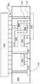
도 28a를 참조하면, 반도체 구조물 또는 디바이스(2800)는, 기판(2802)으로부터 및 분리 영역(2806) 내에 형성된 비평면 활성 영역(예를 들어, 돌출된 핀 부분(2804) 및 서브-핀 영역(2805)을 포함하는 핀 구조물)을 포함한다. 게이트 구조물(2808)은 절연 영역(2806)의 일부의 위 뿐만 아니라 비평면 활성 영역의 돌출된 부분(2804) 위에 배치된다. 도시된 바와 같이, 게이트 구조물(2808)은 게이트 전극(2850) 및 게이트 유전체층(2852)을 포함한다. 한 실시예에서, 도시되지는 않았지만, 게이트 구조물(2808)은 또한 유전체 캡 층을 포함할 수 있다. 게이트 구조물(2808)들은 자기-정렬된 게이트 엣지 분리 구조물(2820)들에 의해 분리된다. 로컬 인터커넥트(2854)는 인접한 게이트 구조물(2808)들을 결합한다. 게이트 컨택트(2814) 및 위에 놓인 게이트 컨택트 비아(2816)도 역시 위에 놓인 금속 인터커넥트(2860)와 함께 본 투시도로부터 볼 수 있고, 이들 모두는 층간 유전체 스택 또는 층(2870)들에 배치된다. 또한 도 28a의 투시도로부터 볼 때, 게이트 컨택트(2814)는, 한 실시예에서, 비평면 활성 영역 위에 배치된다. 도 28a에 역시 도시된 바와 같이, 돌출된 핀 부분(2804)과 서브-핀 영역(2805)의 도핑 프로파일 사이에는 계면(2880)이 존재하지만, 다른 실시예들은 이들 영역들 사이의 도핑 프로파일에서의 이러한 계면을 포함하지 않는다.28A, a semiconductor structure or
한 실시예에서, 다시 도 28a를 참조하면, 돌출된 핀 부분(2804)은, 예를 들어, 산화물 층(2899)에 의해, 상위 및 하위 핀 영역들로 분리된다. 한 실시예에서, 다시 도 28a를 참조하면, 게이트 구조물(2808)들은, 상위 및 하위 게이트 전극 영역들 사이에 배치된 P/N 접합 또는 절연 층을 나타낼 수 있는, 예를 들어, 레벨(2898)에서, 상위 및 하위 게이트 구조물들로 분리된다.In one embodiment, referring again to FIG. 28A, the protruding
도 28b를 참조하면, 게이트 구조물(2808)들은, 자기-정렬된 게이트 엣지 절연 구조물(2820)들에 의해 절연되는, 돌출된 핀 부분(2804)들 위에 배치된 것으로 도시되어 있다. 돌출된 핀 부분(2804)의 소스 및 드레인 영역들(2804A 및 2804B)은 본 투시도에 도시되어 있지만, 이들 영역들은 트렌치 컨택트 구조물과 중첩될 것이라는 것을 이해해야 한다. 한 실시예에서, 소스 및 드레인 영역들(2804A 및 2804B)은 돌출된 핀 부분(2804)의 원래 재료의 도핑된 부분이다. 또 다른 실시예에서, 돌출된 핀 부분(2804)의 재료는 제거되고, 예를 들어 에피텍셜 증착에 의해, 또 다른 반도체 재료로 대체된다. 어느 경우에서도, 소스 및 드레인 영역들(2804A 및 2804B)은 유전체 층(2806)의 높이 아래로, 즉, 서브-핀 영역(2805) 내로 연장될 수 있다.28B,
한 실시예에서, 반도체 구조물 또는 디바이스(2800)는, FinFET 또는 트라이-게이트 디바이스 등의 그러나 이것으로 제한되지 않는 비평면 디바이스이다. 이러한 실시예에서, 대응하는 반도체 채널 영역은 3차원 본체로 구성되거나 형성된다. 한 이러한 실시예에서, 게이트 구조물(2808)들은 3차원 본체의 적어도 상단면(top surface) 및 한 쌍의 측벽을 둘러싼다.In one embodiment, the semiconductor structure or
기판(2802)은, 제작 공정을 견딜 수 있고 전하가 이동할 수 있는 반도체 재료로 구성될 수 있다. 한 실시예에서, 기판(2802)은, 활성 영역(2804)을 형성하기 위해 인, 비소, 붕소 또는 이들의 조합 등의 그러나 이것으로 제한되지 않는 전하 캐리어로 도핑된 결정질 실리콘, 실리콘/게르마늄 또는 게르마늄 층으로 구성된 벌크 기판이다. 한 실시예에서, 벌크 기판(2802)의 실리콘 원자들의 농도는 97%보다 크다. 또 다른 실시예에서, 벌크 기판(2802)은, 별개의 결정질 기판의 최상부에 성장된 에피텍셜 층, 예를 들어 붕소-도핑된 실리콘 단결정 기판의 최상부에 성장된 실리콘 에피텍셜 층으로 구성된다. 벌크 기판(2802)은 대안으로서 III-V족 재료로 구성될 수 있다. 한 실시예에서, 벌크 기판(2802)은, 갈륨 질화물, 갈륨 인화물, 갈륨 비소, 인듐 인화물, 인듐 안티몬화물, 인듐 갈륨 비화물, 알루미늄 갈륨 비화물, 인듐 갈륨 인화물, 또는 이들의 조합 등의 그러나 이것으로 제한되지 않는 III-V족 재료로 구성된다. 한 실시예에서, 벌크 기판(2802)은 Ⅲ-Ⅴ족 재료로 구성되고, 전하-캐리어 도펀트 불순물 원자는, 탄소, 실리콘, 게르마늄, 산소, 황, 셀레늄 또는 텔루륨 등의 것들인데, 이것으로만 제한되지는 않는다.The
절연 영역(2806)은, 아래에 놓인 벌크 기판으로부터 영구 게이트 구조물의 일부를 궁극적으로 전기적으로 절연하거나 그 절연에 기여하거나, 또는 절연 핀 활성 영역 등의 아래에 놓인 벌크 기판 내에 형성된 활성 영역들을 절연하는데 적합한 재료로 구성될 수 있다. 예를 들어, 한 실시예에서, 절연 영역(2806)은, 실리콘 이산화물, 실리콘 산화질화물, 실리콘 질화물, 또는 탄소-도핑된 실리콘 질화물 등의 그러나 이것으로 제한되지 않는 유전체 재료로 구성된다.The
자기-정렬된 게이트 엣지 절연 구조물(2820)은 영구 게이트 구조물의 일부를 서로 전기적으로 절연하거나 그 절연에 기여하는데 적합한 재료로 구성될 수 있다. 예를 들어, 한 실시예에서, 절연 영역(2806)은, 실리콘 이산화물, 실리콘 산화질화물, 실리콘 질화물, 또는 탄소-도핑된 실리콘 질화물 등의 그러나 이것으로 제한되지 않는 유전체 재료로 구성된다.The self-aligned gate
게이트 구조물(2808)은 게이트 전극 스택으로 구성될 수 있고, 게이트 유전체층(2852) 및 게이트 전극 층(2850)을 포함하는 수직으로 적층된 게이트 스택까지 가능할 수 있다. 한 실시예에서, 게이트 전극 스택의 게이트 전극은 금속 게이트로 구성되고 게이트 유전체 층은 하이-K 재료로 구성된다. 예를 들어, 한 실시예에서, 게이트 유전체 층은, 하프늄 산화물, 하프늄 산화질화물, 하프늄 실리케이트, 란탄 산화물, 지르코늄 산화물, 지르코늄 실리케이트, 탄탈 산화물, 바륨 스트론튬 티타네이트, 바륨 티타네이트, 스트론튬 티타네이트, 이트륨 산화물, 알루미늄 산화물, 납 스칸듐 탄탈 산화물, 납 아연 니오브산염, 또는 이들의 조합 등의 그러나 이것으로 제한되지 않는 재료로 구성된다. 또한, 게이트 유전체 층의 일부는 기판(2802)의 최상위 몇 개 층들로부터 형성된 네이티브 산화물(native oxide)의 층을 포함할 수 있다. 한 실시예에서, 게이트 유전체 층은 반도체 재료의 산화물로 구성된 상단 하이-k 부분 및 하위 부분으로 구성된다. 한 실시예에서, 게이트 유전체층은, 하프늄 산화물의 상단 부분과 실리콘 이산화물 또는 실리콘 산화질화물의 하단 부분으로 구성된다.The
한 실시예에서, 게이트 전극은, 금속 질화물, 금속 탄화물, 금속 규화물, 금속 알루미나이드, 하프늄, 지르코늄, 티타늄, 탄탈, 알루미늄, 루테늄, 팔라듐, 백금, 코발트, 니켈 또는 전도성 금속 산화물 등의 그러나 이것으로 제한되지 않는 금속 층으로 구성된다. 특정한 실시예에서, 게이트 전극은, 금속 일함수-설정 층 위에 형성된 비-일함수-설정 충전 재료로 구성된다.In one embodiment, the gate electrode is made of a metal nitride, a metal carbide, a metal silicide, a metal aluminide, hafnium, zirconium, titanium, tantalum, aluminum, ruthenium, palladium, platinum, cobalt, nickel or a conductive metal oxide, It is composed of an unrestricted metal layer. In a particular embodiment, the gate electrode is comprised of a non-work function-setting fill material formed over the metal work function-setting layer.
게이트 전극 스택과 관련된 스페이서는, 자기 정렬된 컨택트 등의, 인접한 도전성 컨택트로부터 영구 게이트 구조물을 궁극적으로 전기적으로 절연하거나 그 절연에 기여하기에 적합한 재료로 구성될 수 있다. 예를 들어, 한 실시예에서, 스페이서는, 실리콘 이산화물, 실리콘 산화질화물, 실리콘 질화물, 또는 탄소-도핑된 실리콘 질화물 등의 그러나 이것으로 제한되지 않는 유전체 재료로 구성된다.The spacers associated with the gate electrode stack may be composed of a material suitable for ultimately electrically insulating or contributing to the isolation of the permanent gate structure from adjacent conductive contacts, such as self-aligned contacts. For example, in one embodiment, the spacers are comprised of a dielectric material such as but not limited to silicon dioxide, silicon oxynitride, silicon nitride, or carbon-doped silicon nitride.
로컬 인터커넥트(2854), 게이트 컨택트(2814), 및 위에 놓인 게이트 컨택트 비아(2816)는 전도성 재료로 구성될 수 있다. 한 실시예에서, 컨택트 또는 비아 중 하나 이상은 금속 종으로 구성된다. 금속 종은, 텅스텐, 니켈, 또는 코발트 등의 순수 금속이건, 금속-금속 합금 또는 금속-반도체 합금(예를 들어, 실리사이드 재료 등) 등의 합금일 수 있다. 하드 마스크 층은 게이트 컨택트(2814)가 놓여 있지 않은 위치들에서 로컬 인터커넥트(2854) 상에 배치될 수 있다. 또한, 로컬 인터커넥트(2854)는 리소그래피 패터닝에 의해 제작되거나, 다른 실시예들에서, 자기-정렬된 게이트 엣지 절연 구조물(2820)의 더 높은 버전들과 정렬되는, 자기-정렬된 인터커넥트 구조물로서 제작될 수 있다.The
(도시되지는 않았지만) 한 실시예에서, 구조물(2800)을 제공하는 것은, 매우 빠듯한 정렬 예산을 동반한 리소그래피 단계의 이용을 제거하면서 본질적으로 기존의 게이트 패턴과 완벽하게 정렬되는 컨택트 패턴의 형성을 수반한다. 한 이러한 실시예에서, 이 접근법은, (예를 들어, 종래에 구현된 건식 또는 플라즈마 에칭과 비교하여) 본질적으로 고도로 선택적인 습식 에칭의 이용에 의한 컨택트 개구의 생성을 가능하게 한다. 한 실시예에서, 컨택트 패턴은, 컨택트 플러그 리소그래피 공정과 조합하여 기존의 게이트 패턴을 이용함으로써 형성된다. 한 이러한 실시예에서, 이 접근법은, 종래의 접근법에서 이용되는 컨택트 패턴을 생성하기 위한 보통은 중요한 리소그래피 동작에 대한 필요성의 제거를 가능하게 한다. 한 실시예에서, 트렌치 컨택트 그리드는 별도로 패터닝되지 않고, 오히려 폴리(게이트) 라인들 사이에 형성된다. 예를 들어, 한 이러한 실시예에서, 트렌치 컨택트 그리드는 게이트 격자 패터닝 이후로서 게이트 격자 절단 이전에 형성된다.In one embodiment (not shown), providing the
또한, 게이트 구조물(2808)은 대체 게이트 공정에 의해 제작될 수 있다. 이러한 방식에서, 폴리실리콘 또는 실리콘 질화물 필러(pillar) 재료 등의 더미 게이트 재료는 제거되어 영구 게이트 전극 재료로 대체될 수 있다. 한 이러한 실시예에서, 영구 게이트 유전체 층도 역시, 더 앞선 처리로부터 전달되는 것과는 대조적으로, 이 공정에서 형성된다. 한 실시예에서, 더미 게이트는 건식 에칭 또는 습식 에칭 공정에 의해 제거된다. 한 실시예에서, 더미 게이트는 다결정 실리콘 또는 비정질 실리콘으로 구성되고 SF6의 이용을 포함한 건식 에칭 공정으로 제거된다. 또 다른 실시예에서, 더미 게이트는 다결정 실리콘 또는 비정질 실리콘으로 구성되고, 수성 NH4OH 또는 테트라메틸암모늄 수산화물의 이용을 포함한 습식 에칭 공정으로 제거된다. 한 실시예에서, 더미 게이트는 실리콘 질화물로 구성되고 수성 인산을 포함한 습식 에칭으로 제거된다.In addition, the
한 실시예에서, 여기서 설명된 하나 이상의 접근법은 본질적으로, 더미 및 대체 게이트 공정을 더미 및 대체 컨택트 공정과 조합하여 구조물(2800)을 달성하는 것을 고려하고 있다. 한 이러한 실시예에서, 대체 컨택트 공정은 대체 게이트 공정 이후에 수행되어 영구 게이트 스택의 적어도 일부의 고온 어닐링을 허용한다. 예를 들어, 특정한 이러한 실시예에서, 예를 들어 게이트 유전체 층이 형성된 이후에 영구 게이트 구조물의 적어도 일부의 어닐링이 약 섭씨 600 ℃ 보다 높은 온도에서 수행된다. 어닐링은 영구 컨택트를 형성하기 전에 수행된다.In one embodiment, the one or more approaches described herein essentially contemplate achieving the
다시 도 28a를 참조하면, 한 실시예에서, 반도체 디바이스는 활성 영역 위에 형성된 게이트 전극의 부분들과 접촉하는 컨택트 구조물을 갖는다. 일반적으로, 게이트의 활성 부분 위 및 트렌치 컨택트 비아와 동일한 층에 (비아 등의) 게이트 컨택트 구조물을 형성하기 전에(예를 들어, 이에 추가하여), 본 발명의 하나 이상의 실시예는 먼저 게이트 정렬된 트렌치 컨택트 공정의 이용을 포함한다. 이러한 공정은, 반도체 구조물 제작을 위한, 예를 들어, 집적 회로 제작을 위한 트렌치 컨택트 구조물을 형성하도록 구현될 수 있다. 한 실시예에서, 트렌치 컨택트 패턴은 기존의 게이트 패턴에 정렬되어 형성된다. 대조적으로, 종래의 접근법은 통상적으로 선택적 컨택트 에칭과 조합하여 기존 게이트 패턴에 대한 리소그래피 컨택트 패턴의 엄격한 정렬을 동반한 추가적인 리소그래피 공정을 포함한다. 예를 들어, 종래의 공정은 컨택트 피쳐들의 별도의 패터닝을 동반한 폴리(게이트) 그리드의 패터닝을 포함할 수 있다.Referring again to Figure 28A, in one embodiment, the semiconductor device has a contact structure in contact with portions of the gate electrode formed over the active region. In general, one or more embodiments of the present invention may be fabricated by first subjecting (for example, by way of example) a gate-contact structure Trench contact process. Such a process can be implemented to form a trench contact structure for fabricating semiconductor structures, e.g., for integrated circuit fabrication. In one embodiment, the trench contact pattern is formed in alignment with an existing gate pattern. In contrast, conventional approaches typically involve additional lithography processes with strict alignment of the lithographic contact pattern to existing gate patterns in combination with selective contact etching. For example, a conventional process may include patterning a poly (gate) grid with separate patterning of contact features.
도 29는 본 발명의 한 구현에 따른 컴퓨팅 디바이스(2900)를 나타낸다. 컴퓨팅 디바이스(2900)는 보드(2902)를 수용한다. 보드(2902)는, 프로세서(2904) 및 적어도 하나의 통신 칩(2906)을 포함한 그러나 이것으로 제한되지 않는 다수의 컴포넌트를 포함할 수 있다. 프로세서(2904)는 보드(2902)에 물리적으로 및 전기적으로 결합된다. 일부 구현들에서, 적어도 하나의 통신 칩(2906)더 역시 보드(2902)에 물리적으로 및 전기적으로 결합된다. 추가의 구현에서, 통신 칩(2906)은 프로세서(2904)의 일부이다.29 illustrates a
그 응용에 따라, 컴퓨팅 디바이스(2900)는, 보드(2902)에 물리적으로 및 전기적으로 결합되거나 결합되지 않을 수 있는 다른 컴포넌트들을 포함할 수 있다. 이들 다른 컴포넌트들은, 휘발성 메모리(예를 들어, DRAM), 비휘발성 메모리(예를 들어, ROM), 플래시 메모리, 그래픽 프로세서, 디지털 신호 프로세서, 크립토 프로세서, 칩셋, 안테나, 디스플레이, 터치스크린 디스플레이, 터치스크린 제어기, 배터리, 오디오 코덱, 비디오 코덱, 전력 증폭기, GPS(global positioning system) 디바이스, 나침반, 가속도계, 자이로스코프, 스피커, 카메라, (하드 디스크 드라이브, 컴팩트 디스크(CD), 디지털 범용 디스크(DVD) 등과 같은) 대용량 저장 디바이스를 포함할 수 있지만, 이것으로 제한되는 것은 아니다.Depending on the application,
통신 칩(2906)은 컴퓨팅 디바이스(2900)와의 데이터 교환을 위한 무선 통신을 가능하게 한다. 용어 "무선(wireless)" 및 그 파생어들은, 비-고체 매체를 통한 변조된 전자기 복사(electromagnetic radiation)를 이용하여 데이터를 전달할 수 있는, 회로, 디바이스, 시스템, 방법, 기술, 통신 채널 등을 기술하는데 사용될 수 있다. 이 용어는 연관된 디바이스가 어떠한 유선도 포함하지 않는다는 것을 암시하는 것은 아니지만, 일부 실시예들에서는 그렇지 않을 수도 있다. 통신 칩(2906)은, Wi-Fi (IEEE 802.11군), WiMAX (IEEE 802.16군), IEEE 802.20, 롱 텀 에볼루션(LTE), Ev-DO, HSPA+, HSDPA+, HSUPA+, EDGE, GSM, GPRS, CDMA, TDMA, DECT, Bluetooth, 그 파생물 뿐만 아니라 3G, 4G, 5G, 및 그 이상으로 표기된 기타 임의의 무선 프로토콜을 포함한 그러나 이것으로 제한되지 않는 다수의 무선 표준이나 프로토콜들 중 임의의 것을 구현할 수 있다. 컴퓨팅 디바이스(2900)는 복수의 통신 칩(2906)을 포함할 수 있다. 예를 들어, 제1 통신 칩(2906)은 Wi-Fi 및 Bluetooth 등의 더 짧은 거리의 무선 통신에 전용되고, 제2 통신 칩(2906)은, GPS, EDGE, GPRS, CDMA, WiMAX, LTE, Ev-DO 등의 더 긴 거리의 무선 통신에 전용될 수도 있다.The communication chip 2906 enables wireless communication for data exchange with the
컴퓨팅 디바이스(2900)의 프로세서(2904)는 프로세서(2904) 내에 팩키징된 집적 회로 다이를 포함한다. 본 발명의 일부 구현들에서, 프로세서의 집적 회로 다이는 본 발명의 실시예의 구현에 따라 구축된 MOS-FET 트랜지스터 등의 하나 이상의 디바이스를 포함한다. 용어 "프로세서"란, 레지스터 및/또는 메모리로부터의 전자적 데이터를 처리하여 그 전자적 데이터를 레지스터 및/또는 메모리에 저장될 수 있는 다른 전자적 데이터로 변환하는 임의의 디바이스 또는 디바이스의 일부를 말한다.The processor 2904 of the
통신 칩(2906)은 또한 통신 칩(2906) 내에 팩키징된 집적 회로 다이를 포함한다. 본 발명의 실시예의 또 다른 구현에 따르면, 통신 칩의 집적 회로 다이는, 본 발명의 실시예의 구현에 따라 구축된, MOS-FET 트랜지스터 등의 하나 이상의 디바이스를 포함한다.The communication chip 2906 also includes an integrated circuit die packaged within the communication chip 2906. According to another implementation of an embodiment of the present invention, the integrated circuit die of a communications chip comprises one or more devices, such as MOS-FET transistors, constructed in accordance with an implementation of an embodiment of the present invention.
추가 구현들에서, 컴퓨팅 디바이스(2900) 내에 수용된 또 다른 컴포넌트는, 본 발명의 실시예의 구현에 따라 구축된, MOS-FET 트랜지스터 등의 하나 이상의 디바이스를 포함하는 집적 회로 다이를 포함할 수 있다.In further implementations, another component housed within the
다양한 구현에서, 컴퓨팅 디바이스(2900)는, 랩탑, 넷북, 노트북, 울트라북, 스마트폰, 태블릿, PDA(personal digital assistant), 울트라 모바일 PC, 모바일 전화, 데스크탑 컴퓨터, 서버, 프린터, 스캐너, 모니터, 셋탑 박스, 오락 제어 유닛, 디지털 카메라, 휴대형 음악 재생기, 또는 디지털 비디오 레코더일 수 있다. 추가 구현에서, 컴퓨팅 디바이스(2900)는, 데이터를 처리하는 기타 임의의 전자 디바이스일 수 있다.In various implementations, the
도 30은 본 발명의 하나 이상의 실시예를 포함하는 인터포저(3000)를 나타낸다. 인터포저(3000)는 제1 기판(3002)을 제2 기판(3004)에 브리징(bridge)하는데 이용되는 개재 기판(intervening substrate)이다. 제1 기판(3002)은 예를 들어 집적 회로 다이일 수 있다. 제2 기판(3004)은, 예를 들어, 메모리 모듈, 컴퓨터 마더보드, 또는 다른 집적 회로 다이일 수 있다. 일반적으로, 인터포저(3000)의 목적은, 접속을 더 넓은 피치로 확산시키거나 접속을 상이한 접속에 리라우팅하는 것이다. 예를 들어, 인터포저(3000)는, 후속해서 제2 기판(3004)에 결합될 수 있는 볼 그리드 어레이(BGA)(3006)에 집적 회로 다이를 결합시킬 수 있다. 일부 실시예들에서, 제1 및 제2 기판(3002/3004)은 인터포저(3000)의 대향 측면들에 부착된다. 다른 실시예들에서, 제1 및 제2 기판(3002/3004)은 인터포저(3000)의 동일한 측면에 부착된다. 추가 실시예들에서, 3개 이상의 기판이 인터포저(3000)에 의해 인터커넥트된다.30 shows an
인터포저(3000)는, 에폭시 수지, 유리섬유-강화된 에폭시 수지, 세라믹 재료, 또는 폴리이미드 등의 중합체 재료로 형성될 수 있다. 추가 구현들에서, 인터포저는, 실리콘, 게르마늄, 및 다른 III-V족 및 IV족 재료 등의, 반도체 기판에서 이용하기 위한 전술된 재료와 동일한 재료를 포함할 수 있는 대안적인 경성 또는 가요성 재료로 형성될 수 있다.The
인터포저는, TSV(through-silicon via)(3012)를 포함한 그러나 이것으로 제한되지 않는 비아(3010) 및 금속 인터커넥트(3008)를 포함할 수 있다. 인터포저(3000)는, 수동 및 능동 디바이스를 포함한, 임베디드 디바이스(3014)를 더 포함할 수 있다. 이러한 디바이스들로는, 커패시터, 디커플링 커패시터, 저항기, 인덕터, 퓨즈, 다이오드, 변압기, 센서, 및 정전 방전(ESD) 디바이스가 포함되지만, 이것으로 제한되지 않는다. 무선 주파수(RF) 디바이스, 전력 증폭기, 전력 관리 디바이스, 안테나, 어레이, 센서 및 MEMS 디바이스 등의 더 복잡한 디바이스가 또한 인터포저(3000) 상에 형성될 수 있다. 본 발명의 실시예에 따르면, 여기서 개시된 장치 또는 프로세스는 인터포저(3000)의 제작에 이용될 수 있다.The interposer may include
따라서, 본 발명의 실시예는 반도체 디바이스의 면적 스케일링을 위한 수직 집적 방식 및 회로 요소 아키텍쳐를 포함한다.Accordingly, embodiments of the present invention include a vertical integration scheme and circuit element architecture for area scaling of semiconductor devices.
한 실시예에서, 인버터 구조물은 상위 영역 및 하위 영역으로 수직으로 분리된 반도체 핀을 포함한다. 제1 복수의 게이트 구조물은 반도체 핀의 상위 영역을 제어하기 위해 포함된다. 제2 복수의 게이트 구조물은 반도체 핀의 하위 영역을 제어하기 위해 포함된다. 제2 복수의 게이트 구조물은 제1 복수의 게이트 구조물의 도전형과는 반대의 도전형을 갖는다.In one embodiment, the inverter structure includes semiconductor pins vertically separated into an upper region and a lower region. A first plurality of gate structures are included for controlling the upper regions of the semiconductor fins. A second plurality of gate structures are included to control sub-regions of the semiconductor fin. The second plurality of gate structures have a conductivity type opposite to that of the first plurality of gate structures.
한 실시예에서, 핀의 상위 영역과 핀의 하위 영역은 절연 층에 의해 분리된다.In one embodiment, the upper region of the pin and the lower region of the pin are separated by an insulating layer.
한 실시예에서, 제1 복수의 게이트 구조물과 제2 복수의 게이트 구조물 중 대응하는 것들은 절연 층에 의해 분리된다.In one embodiment, the corresponding ones of the first plurality of gate structures and the second plurality of gate structures are separated by an insulating layer.
한 실시예에서, 제1 복수의 게이트 구조물과 제2 복수의 게이트 구조물 중 대응하는 것들은 P/N 접합을 형성한다.In one embodiment, the corresponding ones of the first plurality of gate structures and the second plurality of gate structures form a P / N junction.
한 실시예에서, 제1 복수의 게이트 구조물은 복수의 PMOS 게이트 구조물이고, 제2 복수의 게이트 구조물은 복수의 NMOS 게이트 구조물이다.In one embodiment, the first plurality of gate structures is a plurality of PMOS gate structures and the second plurality of gate structures is a plurality of NMOS gate structures.
한 실시예에서, 제1 복수의 게이트 구조물은 반도체 핀의 상단면 위에 및 반도체 핀의 상위 영역의 측벽을 따라 배치되고, 제2 복수의 게이트 구조물은 반도체 핀의 하위 영역의 측벽을 따라 배치된다.In one embodiment, a first plurality of gate structures is disposed over the top surface of the semiconductor fin and along the sidewalls of the upper region of the semiconductor fin, and a second plurality of the gate structures is disposed along the sidewalls of the bottom region of the semiconductor fin.
한 실시예에서, 제2 복수의 게이트 구조물은 또한, 반도체 핀의 하단면(bottom surface) 아래에 배치된다.In one embodiment, the second plurality of gate structures is also disposed below the bottom surface of the semiconductor fin.
한 실시예에서, 패스 게이트 구조물은 상위 영역 및 하위 영역으로 수직으로 분리된 반도체 핀을 포함한다. 제1 복수의 게이트 구조물은 반도체 핀의 상위 영역을 제어하기 위해 포함된다. 제2 복수의 게이트 구조물은 반도체 핀의 하위 영역을 제어하기 위해 포함된다. 제2 복수의 게이트 구조물은 제1 복수의 게이트 구조물의 도전형과 동일한 도전형을 갖는다.In one embodiment, the passgate structure includes semiconductor pins vertically separated into an upper region and a lower region. A first plurality of gate structures are included for controlling the upper regions of the semiconductor fins. A second plurality of gate structures are included to control sub-regions of the semiconductor fin. The second plurality of gate structures have the same conductivity type as the first plurality of gate structures.
한 실시예에서, 핀의 상위 영역과 핀의 하위 영역은 절연 층에 의해 분리된다.In one embodiment, the upper region of the pin and the lower region of the pin are separated by an insulating layer.
한 실시예에서, 제1 복수의 게이트 구조물과 제2 복수의 게이트 구조물 중 대응하는 것들은 절연 층에 의해 분리된다.In one embodiment, the corresponding ones of the first plurality of gate structures and the second plurality of gate structures are separated by an insulating layer.
한 실시예에서, 제1 복수의 게이트 구조물은 복수의 NMOS 게이트 구조물이고, 제2 복수의 게이트 구조물은 복수의 NMOS 게이트 구조물이다.In one embodiment, the first plurality of gate structures is a plurality of NMOS gate structures, and the second plurality of gate structures is a plurality of NMOS gate structures.
한 실시예에서, 제1 복수의 게이트 구조물은 반도체 핀의 상단면 위에 및 반도체 핀의 상위 영역의 측벽을 따라 배치되고, 제2 복수의 게이트 구조물은 반도체 핀의 하위 영역의 측벽을 따라 배치된다.In one embodiment, a first plurality of gate structures is disposed over the top surface of the semiconductor fin and along the sidewalls of the upper region of the semiconductor fin, and a second plurality of the gate structures is disposed along the sidewalls of the bottom region of the semiconductor fin.
한 실시예에서, 제2 복수의 게이트 구조물은 또한 반도체 핀의 하단면 아래에 배치된다.In one embodiment, the second plurality of gate structures is also disposed below the bottom surface of the semiconductor fin.
한 실시예에서, 단일 반도체 핀 상에 회로 요소를 제작하는 방법은 반도체 핀을 형성하는 단계를 포함한다. 이 방법은 또한, 반도체 핀을 상위 영역과 하위 영역으로 수직으로 분리하는 단계를 포함한다. 이 방법은 또한, 반도체 핀의 하위 영역을 제어하기 위한 하위 복수의 게이트 구조물을 형성하는 단계를 포함한다. 이 방법은 또한, 반도체 핀의 상위 영역을 제어하기 위한 상위 복수의 게이트 구조물을 형성하는 단계를 포함한다.In one embodiment, a method of fabricating a circuit element on a single semiconductor fin includes forming a semiconductor fin. The method also includes vertically separating the semiconductor fin into an upper region and a lower region. The method also includes forming a bottom plurality of gate structures for controlling subregions of the semiconductor fin. The method also includes forming a plurality of upper gate structures for controlling an upper region of the semiconductor fin.
한 실시예에서, 상위 복수의 게이트 구조물을 형성하는 단계는, 하위 복수의 게이트 구조물의 도전형과는 반대의 도전형을 갖는 복수의 게이트 구조물을 형성하는 단계를 포함한다.In one embodiment, forming a top plurality of gate structures includes forming a plurality of gate structures having a conductivity type opposite that of the bottom plurality of gate structures.
한 실시예에서, 상위 복수의 게이트 구조물을 형성하는 단계는, 하위 복수의 게이트 구조물의 도전형과 동일한 도전형을 갖는 복수의 게이트 구조물을 형성하는 단계를 포함한다.In one embodiment, forming the upper plurality of gate structures includes forming a plurality of gate structures having the same conductivity type as the lower one of the plurality of gate structures.
한 실시예에서, 반도체 핀을 상위 영역과 하위 영역으로 수직으로 분리하는 단계는 반도체 핀의 상위 영역과 하위 영역 사이에 산화물 층을 형성하는 단계를 포함한다.In one embodiment, vertically separating the semiconductor fin into an upper region and a lower region includes forming an oxide layer between an upper region and a lower region of the semiconductor fin.
한 실시예에서, 반도체 핀의 상위 영역과 하위 영역 사이에 산화물 층을 형성하는 단계는, 반도체 핀의 상위 및 하위 실리콘 층들 사이에서 실리콘 게르마늄 층의 일부를 선택적으로 제거하는 단계를 포함한다.In one embodiment, the step of forming an oxide layer between the upper and lower regions of the semiconductor fin includes selectively removing a portion of the silicon germanium layer between the upper and lower silicon layers of the semiconductor fin.
한 실시예에서, 이 방법은 반도체 핀의 하위 부분을 위한 제1 에피텍셜 소스 및 드레인 영역들을 형성하는 단계, 및 반도체 핀의 상위 부분을 위한 제2 에피텍셜 소스 및 드레인 영역들을 형성하는 단계를 더 포함하고, 제2 에피텍셜 소스 및 드레인 영역들은 제1 에피텍셜 소스 및 드레인 영역들과 반대의 도전형이다.In one embodiment, the method further comprises forming first epitaxial source and drain regions for the lower portion of the semiconductor fin, and forming second epitaxial source and drain regions for the upper portion of the semiconductor fin And the second epitaxial source and drain regions are of opposite conductivity type to the first epitaxial source and drain regions.
한 실시예에서, 이 방법은 반도체 핀의 하위 부분을 위한 제1 에피텍셜 소스 및 드레인 영역들을 형성하는 단계, 및 반도체 핀의 상위 부분을 위한 제2 에피텍셜 소스 및 드레인 영역들을 형성하는 단계를 더 포함하고, 제2 에피텍셜 소스 및 드레인 영역들은 제1 에피텍셜 소스 및 드레인 영역들과 동일한 도전형이다.In one embodiment, the method further comprises forming first epitaxial source and drain regions for the lower portion of the semiconductor fin, and forming second epitaxial source and drain regions for the upper portion of the semiconductor fin And the second epitaxial source and drain regions are of the same conductivity type as the first epitaxial source and drain regions.
한 실시예에서, 하위 복수의 게이트 구조물을 형성하는 단계 및 상위 복수의 게이트 구조물을 형성하는 단계는 대체 게이트 공정을 이용하는 단계를 포함한다.In one embodiment, forming a lower plurality of gate structures and forming a higher plurality of gate structures comprises utilizing a replacement gate process.
Claims (21)
Translated fromKorean상위 영역 및 하위 영역으로 수직으로 분리된 반도체 핀;
상기 반도체 핀의 상기 상위 영역을 제어하기 위한 제1 복수의 게이트 구조물; 및
상기 반도체 핀의 상기 하위 영역을 제어하기 위한 제2 복수의 게이트 구조물
을 포함하고, 상기 제2 복수의 게이트 구조물은 상기 제1 복수의 게이트 구조물의 도전형과는 반대의 도전형을 갖는, 인버터 구조물.As an inverter structure,
A semiconductor pin vertically separated into an upper region and a lower region;
A first plurality of gate structures for controlling the upper region of the semiconductor fin; And
A second plurality of gate structures for controlling said sub-
Wherein the second plurality of gate structures have a conductivity type opposite to the conductivity type of the first plurality of gate structures.
상위 영역 및 하위 영역으로 수직으로 분리된 반도체 핀;
상기 반도체 핀의 상기 상위 영역을 제어하기 위한 제1 복수의 게이트 구조물; 및
상기 반도체 핀의 상기 하위 영역을 제어하기 위한 제2 복수의 게이트 구조물
을 포함하고, 상기 제2 복수의 게이트 구조물은 상기 제1 복수의 게이트 구조물의 도전형과 동일한 도전형을 갖는, 패스 게이트 구조물.As a passgate structure,
A semiconductor pin vertically separated into an upper region and a lower region;
A first plurality of gate structures for controlling the upper region of the semiconductor fin; And
A second plurality of gate structures for controlling said sub-
Wherein the second plurality of gate structures have the same conductivity type as the conductivity type of the first plurality of gate structures.
반도체 핀을 형성하는 단계;
상기 반도체 핀을 상위 영역과 하위 영역으로 수직으로 분리하는 단계;
상기 반도체 핀의 상기 하위 영역을 제어하기 위한 하위 복수의 게이트 구조물을 형성하는 단계; 및
상기 반도체 핀의 상기 상위 영역을 제어하기 위한 상위 복수의 게이트 구조물을 형성하는 단계
를 포함하는 방법.A method of fabricating a circuit element on a single semiconductor pin,
Forming a semiconductor fin;
Vertically separating the semiconductor fin into an upper region and a lower region;
Forming a bottom plurality of gate structures for controlling the bottom region of the semiconductor fin; And
Forming a plurality of upper gate structures for controlling the upper regions of the semiconductor fins
≪ / RTI >
상기 반도체 핀의 상기 하위 부분을 위한 제1 에피텍셜 소스 및 드레인 영역들을 형성하는 단계; 및
상기 반도체 핀의 상기 상위 부분을 위한 제2 에피텍셜 소스 및 드레인 영역들을 형성하는 단계를 추가로 포함하고, 상기 제2 에피텍셜 소스 및 드레인 영역들은 상기 제1 에피텍셜 소스 및 드레인 영역들과 반대의 도전형인, 방법.15. The method of claim 14,
Forming first epitaxial source and drain regions for the lower portion of the semiconductor fin; And
Further comprising forming second epitaxial source and drain regions for the upper portion of the semiconductor fin, wherein the second epitaxial source and drain regions are formed in a region opposite to the first epitaxial source and drain regions The method is challenging.
상기 반도체 핀의 상기 하위 부분을 위한 제1 에피텍셜 소스 및 드레인 영역들을 형성하는 단계; 및
상기 반도체 핀의 상기 상위 부분을 위한 제2 에피텍셜 소스 및 드레인 영역들을 형성하는 단계를 추가로 포함하고, 상기 제2 에피텍셜 소스 및 드레인 영역들은 상기 제1 에피텍셜 소스 및 드레인 영역들과 동일한 도전형인, 방법.15. The method of claim 14,
Forming first epitaxial source and drain regions for the lower portion of the semiconductor fin; And
Further comprising forming second epitaxial source and drain regions for the upper portion of the semiconductor fin, wherein the second epitaxial source and drain regions have the same conductivity as the first epitaxial source and drain regions Brother, way.
Applications Claiming Priority (1)
| Application Number | Priority Date | Filing Date | Title |
|---|---|---|---|
| PCT/US2015/036286WO2016204755A1 (en) | 2015-06-17 | 2015-06-17 | Vertical integration scheme and circuit elements architecture for area scaling of semiconductor devices |
Publications (1)
| Publication Number | Publication Date |
|---|---|
| KR20180018497Atrue KR20180018497A (en) | 2018-02-21 |
Family
ID=57545579
Family Applications (1)
| Application Number | Title | Priority Date | Filing Date |
|---|---|---|---|
| KR1020177032875ACeasedKR20180018497A (en) | 2015-06-17 | 2015-06-17 | Vertical integration method and circuit element architecture for area scaling of semiconductor devices |
Country Status (6)
| Country | Link |
|---|---|
| US (4) | US10304946B2 (en) |
| EP (1) | EP3311416B1 (en) |
| KR (1) | KR20180018497A (en) |
| CN (1) | CN107924943B (en) |
| TW (1) | TW201712807A (en) |
| WO (1) | WO2016204755A1 (en) |
Cited By (2)
| Publication number | Priority date | Publication date | Assignee | Title |
|---|---|---|---|---|
| KR20200120883A (en)* | 2019-04-12 | 2020-10-22 | 타이완 세미콘덕터 매뉴팩쳐링 컴퍼니 리미티드 | Integrated circuit |
| US12218132B2 (en) | 2019-04-12 | 2025-02-04 | Taiwan Semiconductor Manufacturing Co., Ltd. | Integrated circuit |
Families Citing this family (26)
| Publication number | Priority date | Publication date | Assignee | Title |
|---|---|---|---|---|
| WO2016204755A1 (en)* | 2015-06-17 | 2016-12-22 | Intel Corporation | Vertical integration scheme and circuit elements architecture for area scaling of semiconductor devices |
| US10790281B2 (en) | 2015-12-03 | 2020-09-29 | Intel Corporation | Stacked channel structures for MOSFETs |
| US10074605B2 (en)* | 2016-06-30 | 2018-09-11 | Taiwan Semiconductor Manufacturing Co., Ltd. | Memory cell and array structure having a plurality of bit lines |
| DE102017124223B4 (en) | 2017-08-30 | 2022-02-24 | Taiwan Semiconductor Manufacturing Co. Ltd. | Semiconductor structure with fins and isolation fins and method for their manufacture |
| US10943830B2 (en)* | 2017-08-30 | 2021-03-09 | Taiwan Semiconductor Manufacturing Co., Ltd. | Self-aligned structure for semiconductor devices |
| US11075198B2 (en)* | 2018-01-08 | 2021-07-27 | Intel Corporation | Stacked transistor architecture having diverse fin geometry |
| US11233152B2 (en)* | 2018-06-25 | 2022-01-25 | Intel Corporation | Self-aligned gate endcap (SAGE) architectures with gate-all-around devices |
| US11374004B2 (en) | 2018-06-29 | 2022-06-28 | Intel Corporation | Pedestal fin structure for stacked transistor integration |
| US11742346B2 (en) | 2018-06-29 | 2023-08-29 | Intel Corporation | Interconnect techniques for electrically connecting source/drain regions of stacked transistors |
| US11348916B2 (en) | 2018-06-29 | 2022-05-31 | Intel Corporation | Leave-behind protective layer having secondary purpose |
| US11616060B2 (en) | 2018-06-29 | 2023-03-28 | Intel Corporation | Techniques for forming gate structures for transistors arranged in a stacked configuration on a single fin structure |
| US11605565B2 (en) | 2018-12-28 | 2023-03-14 | Intel Corporation | Three dimensional integrated circuits with stacked transistors |
| KR102635671B1 (en)* | 2019-03-21 | 2024-02-14 | 에스케이하이닉스 주식회사 | Semiconductor device |
| US11011528B2 (en) | 2019-05-08 | 2021-05-18 | International Business Machines Corporation | Asymmetric gate edge spacing for SRAM structures |
| US10833003B1 (en)* | 2019-05-31 | 2020-11-10 | Taiwan Semiconductor Manufacturing Co., Ltd. | Integrated circuits with backside power rails |
| TWI747308B (en)* | 2019-06-14 | 2021-11-21 | 日商索尼半導體解決方案公司 | Semiconductor device |
| US20210202472A1 (en)* | 2019-12-27 | 2021-07-01 | Intel Corporation | Integrated circuit structures including backside vias |
| US12224349B2 (en) | 2020-05-07 | 2025-02-11 | Intel Corporation | Self-aligned gate endcap (SAGE) architectures with vertical sidewalls |
| DE102020128271A1 (en)* | 2020-05-20 | 2021-11-25 | Taiwan Semiconductor Manufacturing Co., Ltd. | Dummy fin profile control for enlarging the gate process window |
| US11600717B2 (en) | 2020-05-20 | 2023-03-07 | Taiwan Semiconductor Manufacturing Co., Ltd | Dummy FIN profile control to enlarge gate process window |
| US11735585B2 (en)* | 2021-01-18 | 2023-08-22 | Samsung Electronics Co., Ltd. | Stacked semiconductor device having mirror-symmetric pattern |
| US12310072B2 (en) | 2021-12-10 | 2025-05-20 | International Business Machines Corporation | Middle of line structure with stacked devices |
| US20230197854A1 (en)* | 2021-12-16 | 2023-06-22 | Intel Corporation | Integrated circuit structures having dielectric anchor and confined epitaxial source or drain structure |
| US20230197569A1 (en)* | 2021-12-20 | 2023-06-22 | Intel Corporation | Frontside and backside epi contact |
| US12142526B2 (en)* | 2022-03-23 | 2024-11-12 | International Business Machines Corporation | Stacked device with buried interconnect |
| US20240096951A1 (en)* | 2022-09-16 | 2024-03-21 | International Business Machines Corporation | Stacked fets with contact placeholder structures |
Family Cites Families (21)
| Publication number | Priority date | Publication date | Assignee | Title |
|---|---|---|---|---|
| US6229161B1 (en) | 1998-06-05 | 2001-05-08 | Stanford University | Semiconductor capacitively-coupled NDR device and its applications in high-density high-speed memories and in power switches |
| US7138685B2 (en) | 2002-12-11 | 2006-11-21 | International Business Machines Corporation | Vertical MOSFET SRAM cell |
| US6943407B2 (en) | 2003-06-17 | 2005-09-13 | International Business Machines Corporation | Low leakage heterojunction vertical transistors and high performance devices thereof |
| KR100702011B1 (en)* | 2005-03-16 | 2007-03-30 | 삼성전자주식회사 | CMOS SRAM Cells Employing Multiple Gate Transistors and Methods of Manufacturing the Same |
| KR100645065B1 (en) | 2005-06-23 | 2006-11-10 | 삼성전자주식회사 | Fin Field Effect Transistor, Nonvolatile Memory Device Having Same and Forming Method Thereof |
| KR100625933B1 (en)* | 2005-09-29 | 2006-09-18 | 매그나칩 반도체 유한회사 | Semiconductor device and manufacturing method thereof |
| US7745270B2 (en) | 2007-12-28 | 2010-06-29 | Intel Corporation | Tri-gate patterning using dual layer gate stack |
| US8294511B2 (en)* | 2010-11-19 | 2012-10-23 | Micron Technology, Inc. | Vertically stacked fin transistors and methods of fabricating and operating the same |
| US8415250B2 (en)* | 2011-04-29 | 2013-04-09 | International Business Machines Corporation | Method of forming silicide contacts of different shapes selectively on regions of a semiconductor device |
| JP2013021274A (en) | 2011-07-14 | 2013-01-31 | Toshiba Corp | Semiconductor device |
| US8866214B2 (en)* | 2011-10-12 | 2014-10-21 | International Business Machines Corporation | Vertical transistor having an asymmetric gate |
| CN107068753B (en)* | 2011-12-19 | 2020-09-04 | 英特尔公司 | Pulsed laser annealing process of transistors by partial melting of raised source-drain |
| US9236476B2 (en)* | 2011-12-28 | 2016-01-12 | Intel Corporation | Techniques and configuration for stacking transistors of an integrated circuit device |
| US8659097B2 (en)* | 2012-01-16 | 2014-02-25 | Taiwan Semiconductor Manufacturing Company, Ltd. | Control fin heights in FinFET structures |
| KR101986534B1 (en)* | 2012-06-04 | 2019-06-07 | 삼성전자주식회사 | Semiconductor device having embedded strain-inducing pattern and method of forming the same |
| US9111801B2 (en)* | 2013-04-04 | 2015-08-18 | Stmicroelectronics, Inc. | Integrated circuit devices and fabrication techniques |
| US9263338B2 (en) | 2013-10-23 | 2016-02-16 | Stmicroelectronics, Inc. | Semiconductor device including vertically spaced semiconductor channel structures and related methods |
| US9048303B1 (en)* | 2014-01-30 | 2015-06-02 | Infineon Technologies Austria Ag | Group III-nitride-based enhancement mode transistor |
| US10263108B2 (en)* | 2014-08-22 | 2019-04-16 | Taiwan Semiconductor Manufacturing Company, Ltd. | Metal-insensitive epitaxy formation |
| US9601617B2 (en)* | 2015-01-23 | 2017-03-21 | Qualcomm Incorporated | Fabrication of a transistor including a tunneling layer |
| WO2016204755A1 (en)* | 2015-06-17 | 2016-12-22 | Intel Corporation | Vertical integration scheme and circuit elements architecture for area scaling of semiconductor devices |
- 2015
- 2015-06-17WOPCT/US2015/036286patent/WO2016204755A1/ennot_activeCeased
- 2015-06-17CNCN201580080106.XApatent/CN107924943B/enactiveActive
- 2015-06-17KRKR1020177032875Apatent/KR20180018497A/ennot_activeCeased
- 2015-06-17EPEP15895802.5Apatent/EP3311416B1/enactiveActive
- 2015-06-17USUS15/570,965patent/US10304946B2/ennot_activeExpired - Fee Related
- 2016
- 2016-05-10TWTW105114453Apatent/TW201712807A/enunknown
- 2019
- 2019-04-26USUS16/396,088patent/US10847635B2/enactiveActive
- 2020
- 2020-10-26USUS17/080,458patent/US11522072B2/enactiveActive
- 2022
- 2022-10-31USUS17/978,038patent/US12310044B2/enactiveActive
Cited By (4)
| Publication number | Priority date | Publication date | Assignee | Title |
|---|---|---|---|---|
| KR20200120883A (en)* | 2019-04-12 | 2020-10-22 | 타이완 세미콘덕터 매뉴팩쳐링 컴퍼니 리미티드 | Integrated circuit |
| US11374003B2 (en) | 2019-04-12 | 2022-06-28 | Taiwan Semiconductor Manufacturing Co., Ltd. | Integrated circuit |
| US12218132B2 (en) | 2019-04-12 | 2025-02-04 | Taiwan Semiconductor Manufacturing Co., Ltd. | Integrated circuit |
| US12237332B2 (en) | 2019-04-12 | 2025-02-25 | Taiwan Semiconductor Manufacturing Co., Ltd. | Integrated circuit |
Also Published As
| Publication number | Publication date |
|---|---|
| EP3311416A4 (en) | 2019-01-16 |
| US20190252525A1 (en) | 2019-08-15 |
| US12310044B2 (en) | 2025-05-20 |
| US20180204932A1 (en) | 2018-07-19 |
| US10847635B2 (en) | 2020-11-24 |
| US20210043755A1 (en) | 2021-02-11 |
| CN107924943A (en) | 2018-04-17 |
| TW201712807A (en) | 2017-04-01 |
| EP3311416A1 (en) | 2018-04-25 |
| CN107924943B (en) | 2021-04-13 |
| US20230046755A1 (en) | 2023-02-16 |
| WO2016204755A1 (en) | 2016-12-22 |
| US11522072B2 (en) | 2022-12-06 |
| EP3311416B1 (en) | 2023-08-23 |
| US10304946B2 (en) | 2019-05-28 |
Similar Documents
| Publication | Publication Date | Title |
|---|---|---|
| US12310044B2 (en) | Vertical integration scheme and circuit elements architecture for area scaling of semiconductor devices | |
| US11581315B2 (en) | Self-aligned gate edge trigate and finFET devices | |
| US11876121B2 (en) | Self-aligned gate endcap (SAGE) architecture having gate or contact plugs | |
| US11705453B2 (en) | Self-aligned gate endcap (SAGE) architecture having local interconnects | |
| CN111383996A (en) | Self-aligned stacked GE/SI CMOS transistor structure | |
| US12199101B2 (en) | Self-aligned gate endcap (SAGE) architecture having gate contacts | |
| EP4109523A1 (en) | Buried power rail with a silicide layer for well biasing | |
| US12414327B2 (en) | Lateral confinement of source drain epitaxial growth in non-planar transistor for cell height scaling | |
| TWI849127B (en) | Self-aligned gate endcap (sage) architecture having vertical transistor with sage gate structure | |
| TW202213625A (en) | Gate and fin trim isolation for advanced integrated circuit structure fabrication |
Legal Events
| Date | Code | Title | Description |
|---|---|---|---|
| PA0105 | International application | Patent event date:20171114 Patent event code:PA01051R01D Comment text:International Patent Application | |
| PG1501 | Laying open of application | ||
| A201 | Request for examination | ||
| PA0201 | Request for examination | Patent event code:PA02012R01D Patent event date:20200617 Comment text:Request for Examination of Application | |
| E902 | Notification of reason for refusal | ||
| PE0902 | Notice of grounds for rejection | Comment text:Notification of reason for refusal Patent event date:20210430 Patent event code:PE09021S01D | |
| E902 | Notification of reason for refusal | ||
| PE0902 | Notice of grounds for rejection | Comment text:Notification of reason for refusal Patent event date:20210524 Patent event code:PE09021S01D | |
| AMND | Amendment | ||
| E601 | Decision to refuse application | ||
| PE0601 | Decision on rejection of patent | Patent event date:20211130 Comment text:Decision to Refuse Application Patent event code:PE06012S01D Patent event date:20210524 Comment text:Notification of reason for refusal Patent event code:PE06011S01I Patent event date:20210430 Comment text:Notification of reason for refusal Patent event code:PE06011S01I | |
| AMND | Amendment | ||
| PX0901 | Re-examination | Patent event code:PX09011S01I Patent event date:20211130 Comment text:Decision to Refuse Application Patent event code:PX09012R01I Patent event date:20210723 Comment text:Amendment to Specification, etc. | |
| PX0601 | Decision of rejection after re-examination | Comment text:Decision to Refuse Application Patent event code:PX06014S01D Patent event date:20220127 Comment text:Amendment to Specification, etc. Patent event code:PX06012R01I Patent event date:20211229 Comment text:Decision to Refuse Application Patent event code:PX06011S01I Patent event date:20211130 Comment text:Amendment to Specification, etc. Patent event code:PX06012R01I Patent event date:20210723 Comment text:Notification of reason for refusal Patent event code:PX06013S01I Patent event date:20210524 Comment text:Notification of reason for refusal Patent event code:PX06013S01I Patent event date:20210430 | |
| X601 | Decision of rejection after re-examination |