KR20180018413A - Atomic layer etching using a boron-containing gas and hydrogen fluoride gas - Google Patents
Atomic layer etching using a boron-containing gas and hydrogen fluoride gasDownload PDFInfo
- Publication number
- KR20180018413A KR20180018413AKR1020170101457AKR20170101457AKR20180018413AKR 20180018413 AKR20180018413 AKR 20180018413AKR 1020170101457 AKR1020170101457 AKR 1020170101457AKR 20170101457 AKR20170101457 AKR 20170101457AKR 20180018413 AKR20180018413 AKR 20180018413A
- Authority
- KR
- South Korea
- Prior art keywords
- boron
- substrate
- gas
- oxide film
- metal oxide
- Prior art date
- Legal status (The legal status is an assumption and is not a legal conclusion. Google has not performed a legal analysis and makes no representation as to the accuracy of the status listed.)
- Granted
Links
- 239000007789gasSubstances0.000titleclaimsabstractdescription65
- 229910052796boronInorganic materials0.000titleclaimsabstractdescription49
- ZOXJGFHDIHLPTG-UHFFFAOYSA-NBoronChemical compound[B]ZOXJGFHDIHLPTG-UHFFFAOYSA-N0.000titleclaimsabstractdescription37
- 238000005530etchingMethods0.000titleclaimsabstractdescription12
- KRHYYFGTRYWZRS-UHFFFAOYSA-NFluoraneChemical compoundFKRHYYFGTRYWZRS-UHFFFAOYSA-N0.000titleclaimsabstractdescription9
- 229910000040hydrogen fluorideInorganic materials0.000titleclaimsdescription7
- 239000000758substrateSubstances0.000claimsabstractdescription63
- 238000000034methodMethods0.000claimsabstractdescription54
- 229910044991metal oxideInorganic materials0.000claimsabstractdescription38
- 150000004706metal oxidesChemical class0.000claimsabstractdescription38
- 239000002344surface layerSubstances0.000claimsabstractdescription28
- 239000010410layerSubstances0.000claimsabstractdescription11
- -1boron halideChemical class0.000claimsdescription12
- 229910018072Al 2 O 3Inorganic materials0.000claimsdescription7
- UORVGPXVDQYIDP-UHFFFAOYSA-NboraneChemical compoundBUORVGPXVDQYIDP-UHFFFAOYSA-N0.000claimsdescription6
- 229910010277boron hydrideInorganic materials0.000claimsdescription6
- 239000011261inert gasSubstances0.000claimsdescription6
- 229910021193La 2 O 3Inorganic materials0.000claimsdescription5
- 229910010413TiO 2Inorganic materials0.000claimsdescription5
- 125000000962organic groupChemical group0.000claimsdescription5
- YCKRFDGAMUMZLT-UHFFFAOYSA-NFluorine atomChemical compound[F]YCKRFDGAMUMZLT-UHFFFAOYSA-N0.000claimsdescription2
- 229910052731fluorineInorganic materials0.000claimsdescription2
- 239000011737fluorineSubstances0.000claimsdescription2
- 239000002184metalSubstances0.000claimsdescription2
- 238000010926purgeMethods0.000claims2
- 230000001590oxidative effectEffects0.000claims1
- 238000006243chemical reactionMethods0.000description13
- 239000006227byproductSubstances0.000description7
- 239000004065semiconductorSubstances0.000description6
- 239000000463materialSubstances0.000description5
- 238000004519manufacturing processMethods0.000description3
- XKRFYHLGVUSROY-UHFFFAOYSA-NArgonChemical compound[Ar]XKRFYHLGVUSROY-UHFFFAOYSA-N0.000description2
- 238000000231atomic layer depositionMethods0.000description2
- 238000010586diagramMethods0.000description2
- 238000005516engineering processMethods0.000description2
- 230000004048modificationEffects0.000description2
- 238000012986modificationMethods0.000description2
- IJGRMHOSHXDMSA-UHFFFAOYSA-NAtomic nitrogenChemical compoundN#NIJGRMHOSHXDMSA-UHFFFAOYSA-N0.000description1
- UFHFLCQGNIYNRP-UHFFFAOYSA-NHydrogenChemical class[H][H]UFHFLCQGNIYNRP-UHFFFAOYSA-N0.000description1
- 150000001408amidesChemical class0.000description1
- 229910052786argonInorganic materials0.000description1
- 229910052736halogenInorganic materials0.000description1
- 150000002367halogensChemical class0.000description1
- 239000001257hydrogenSubstances0.000description1
- 229910052739hydrogenInorganic materials0.000description1
- 238000003672processing methodMethods0.000description1
- 238000001179sorption measurementMethods0.000description1
- 239000000126substanceSubstances0.000description1
- 230000002123temporal effectEffects0.000description1
Images


Classifications
- H—ELECTRICITY
- H01—ELECTRIC ELEMENTS
- H01L—SEMICONDUCTOR DEVICES NOT COVERED BY CLASS H10
- H01L21/00—Processes or apparatus adapted for the manufacture or treatment of semiconductor or solid state devices or of parts thereof
- H01L21/02—Manufacture or treatment of semiconductor devices or of parts thereof
- H01L21/04—Manufacture or treatment of semiconductor devices or of parts thereof the devices having potential barriers, e.g. a PN junction, depletion layer or carrier concentration layer
- H01L21/18—Manufacture or treatment of semiconductor devices or of parts thereof the devices having potential barriers, e.g. a PN junction, depletion layer or carrier concentration layer the devices having semiconductor bodies comprising elements of Group IV of the Periodic Table or AIIIBV compounds with or without impurities, e.g. doping materials
- H01L21/30—Treatment of semiconductor bodies using processes or apparatus not provided for in groups H01L21/20 - H01L21/26
- H01L21/302—Treatment of semiconductor bodies using processes or apparatus not provided for in groups H01L21/20 - H01L21/26 to change their surface-physical characteristics or shape, e.g. etching, polishing, cutting
- H01L21/306—Chemical or electrical treatment, e.g. electrolytic etching
- H01L21/3065—Plasma etching; Reactive-ion etching
- H—ELECTRICITY
- H01—ELECTRIC ELEMENTS
- H01L—SEMICONDUCTOR DEVICES NOT COVERED BY CLASS H10
- H01L21/00—Processes or apparatus adapted for the manufacture or treatment of semiconductor or solid state devices or of parts thereof
- H01L21/02—Manufacture or treatment of semiconductor devices or of parts thereof
- H01L21/04—Manufacture or treatment of semiconductor devices or of parts thereof the devices having potential barriers, e.g. a PN junction, depletion layer or carrier concentration layer
- H01L21/18—Manufacture or treatment of semiconductor devices or of parts thereof the devices having potential barriers, e.g. a PN junction, depletion layer or carrier concentration layer the devices having semiconductor bodies comprising elements of Group IV of the Periodic Table or AIIIBV compounds with or without impurities, e.g. doping materials
- H01L21/30—Treatment of semiconductor bodies using processes or apparatus not provided for in groups H01L21/20 - H01L21/26
- H01L21/31—Treatment of semiconductor bodies using processes or apparatus not provided for in groups H01L21/20 - H01L21/26 to form insulating layers thereon, e.g. for masking or by using photolithographic techniques; After treatment of these layers; Selection of materials for these layers
- H01L21/3105—After-treatment
- H01L21/311—Etching the insulating layers by chemical or physical means
- H01L21/31105—Etching inorganic layers
- H01L21/31111—Etching inorganic layers by chemical means
- H01L21/31116—Etching inorganic layers by chemical means by dry-etching
- C—CHEMISTRY; METALLURGY
- C01—INORGANIC CHEMISTRY
- C01B—NON-METALLIC ELEMENTS; COMPOUNDS THEREOF; METALLOIDS OR COMPOUNDS THEREOF NOT COVERED BY SUBCLASS C01C
- C01B7/00—Halogens; Halogen acids
- C01B7/19—Fluorine; Hydrogen fluoride
- C01B7/191—Hydrogen fluoride
- H—ELECTRICITY
- H01—ELECTRIC ELEMENTS
- H01L—SEMICONDUCTOR DEVICES NOT COVERED BY CLASS H10
- H01L21/00—Processes or apparatus adapted for the manufacture or treatment of semiconductor or solid state devices or of parts thereof
- H01L21/02—Manufacture or treatment of semiconductor devices or of parts thereof
- H01L21/02041—Cleaning
- H01L21/02043—Cleaning before device manufacture, i.e. Begin-Of-Line process
- H01L21/02046—Dry cleaning only
- H—ELECTRICITY
- H01—ELECTRIC ELEMENTS
- H01L—SEMICONDUCTOR DEVICES NOT COVERED BY CLASS H10
- H01L21/00—Processes or apparatus adapted for the manufacture or treatment of semiconductor or solid state devices or of parts thereof
- H01L21/02—Manufacture or treatment of semiconductor devices or of parts thereof
- H01L21/02104—Forming layers
- H01L21/02107—Forming insulating materials on a substrate
- H01L21/02225—Forming insulating materials on a substrate characterised by the process for the formation of the insulating layer
- H01L21/0226—Forming insulating materials on a substrate characterised by the process for the formation of the insulating layer formation by a deposition process
- H01L21/02263—Forming insulating materials on a substrate characterised by the process for the formation of the insulating layer formation by a deposition process deposition from the gas or vapour phase
- H01L21/02271—Forming insulating materials on a substrate characterised by the process for the formation of the insulating layer formation by a deposition process deposition from the gas or vapour phase deposition by decomposition or reaction of gaseous or vapour phase compounds, i.e. chemical vapour deposition
- H01L21/0228—Forming insulating materials on a substrate characterised by the process for the formation of the insulating layer formation by a deposition process deposition from the gas or vapour phase deposition by decomposition or reaction of gaseous or vapour phase compounds, i.e. chemical vapour deposition deposition by cyclic CVD, e.g. ALD, ALE, pulsed CVD
- H—ELECTRICITY
- H01—ELECTRIC ELEMENTS
- H01L—SEMICONDUCTOR DEVICES NOT COVERED BY CLASS H10
- H01L21/00—Processes or apparatus adapted for the manufacture or treatment of semiconductor or solid state devices or of parts thereof
- H01L21/02—Manufacture or treatment of semiconductor devices or of parts thereof
- H01L21/04—Manufacture or treatment of semiconductor devices or of parts thereof the devices having potential barriers, e.g. a PN junction, depletion layer or carrier concentration layer
- H01L21/18—Manufacture or treatment of semiconductor devices or of parts thereof the devices having potential barriers, e.g. a PN junction, depletion layer or carrier concentration layer the devices having semiconductor bodies comprising elements of Group IV of the Periodic Table or AIIIBV compounds with or without impurities, e.g. doping materials
- H01L21/30—Treatment of semiconductor bodies using processes or apparatus not provided for in groups H01L21/20 - H01L21/26
- H01L21/31—Treatment of semiconductor bodies using processes or apparatus not provided for in groups H01L21/20 - H01L21/26 to form insulating layers thereon, e.g. for masking or by using photolithographic techniques; After treatment of these layers; Selection of materials for these layers
- H01L21/3105—After-treatment
- H01L21/311—Etching the insulating layers by chemical or physical means
- H01L21/31105—Etching inorganic layers
- H01L21/31111—Etching inorganic layers by chemical means
- H01L21/31116—Etching inorganic layers by chemical means by dry-etching
- H01L21/31122—Etching inorganic layers by chemical means by dry-etching of layers not containing Si, e.g. PZT, Al2O3
- C—CHEMISTRY; METALLURGY
- C01—INORGANIC CHEMISTRY
- C01B—NON-METALLIC ELEMENTS; COMPOUNDS THEREOF; METALLOIDS OR COMPOUNDS THEREOF NOT COVERED BY SUBCLASS C01C
- C01B35/00—Boron; Compounds thereof
- C01B35/02—Boron; Borides
- C—CHEMISTRY; METALLURGY
- C01—INORGANIC CHEMISTRY
- C01B—NON-METALLIC ELEMENTS; COMPOUNDS THEREOF; METALLOIDS OR COMPOUNDS THEREOF NOT COVERED BY SUBCLASS C01C
- C01B35/00—Boron; Compounds thereof
- C01B35/06—Boron halogen compounds
- H—ELECTRICITY
- H01—ELECTRIC ELEMENTS
- H01L—SEMICONDUCTOR DEVICES NOT COVERED BY CLASS H10
- H01L21/00—Processes or apparatus adapted for the manufacture or treatment of semiconductor or solid state devices or of parts thereof
- H01L21/02—Manufacture or treatment of semiconductor devices or of parts thereof
- H01L21/04—Manufacture or treatment of semiconductor devices or of parts thereof the devices having potential barriers, e.g. a PN junction, depletion layer or carrier concentration layer
- H01L21/18—Manufacture or treatment of semiconductor devices or of parts thereof the devices having potential barriers, e.g. a PN junction, depletion layer or carrier concentration layer the devices having semiconductor bodies comprising elements of Group IV of the Periodic Table or AIIIBV compounds with or without impurities, e.g. doping materials
- H01L21/30—Treatment of semiconductor bodies using processes or apparatus not provided for in groups H01L21/20 - H01L21/26
- H01L21/31—Treatment of semiconductor bodies using processes or apparatus not provided for in groups H01L21/20 - H01L21/26 to form insulating layers thereon, e.g. for masking or by using photolithographic techniques; After treatment of these layers; Selection of materials for these layers
- H01L21/3105—After-treatment
- H01L21/311—Etching the insulating layers by chemical or physical means
- H01L21/31127—Etching organic layers
- H01L21/31133—Etching organic layers by chemical means
- H01L21/31138—Etching organic layers by chemical means by dry-etching
Landscapes
- Engineering & Computer Science (AREA)
- Chemical & Material Sciences (AREA)
- Physics & Mathematics (AREA)
- General Physics & Mathematics (AREA)
- Manufacturing & Machinery (AREA)
- Computer Hardware Design (AREA)
- Microelectronics & Electronic Packaging (AREA)
- Power Engineering (AREA)
- Condensed Matter Physics & Semiconductors (AREA)
- Inorganic Chemistry (AREA)
- Chemical Kinetics & Catalysis (AREA)
- Organic Chemistry (AREA)
- General Chemical & Material Sciences (AREA)
- Plasma & Fusion (AREA)
- Drying Of Semiconductors (AREA)
Abstract
Translated fromKoreanDescription
Translated fromKorean[본원과 관련된 상호 참조 문헌][Cross-references related to the present invention]
본 출원은 여기에 전체가 참조로 포함된 미국 가출원 62/373,232(출원일 : 2016년 8월 10일)에 관한 것이고 이에 대하여 우선권을 주장한다.This application is related to and claims priority to U.S. Provisional Application No. 62 / 373,232, filed on August 10, 2016, which is incorporated herein by reference in its entirety.
본 발명은 반도체 제조 및 반도체 디바이스의 분야에 관한 것이고 특히 붕소 함유 가스와 플루오르화 수소 가스를 이용한 기판의 ALE(atomic layer etching)에 관한 것이다.Field of the Invention The present invention relates to the field of semiconductor manufacturing and semiconductor devices, and more particularly to atomic layer etching (ALE) of a substrate using boron-containing gas and hydrogen fluoride gas.
디바이스 피처 크기가 계속 확장됨에 따라 미세 피처의 에칭을 정확하게 제어하는 것이 중요한 과제로 대두되고 있다. 10 nm 이하의 고도로 확장된 노드의 경우, 디바이스들은 원자 스케일 확장 충실도 또는 매우 엄격한 프로세스 변동성이 필요하다. 변동성으로 인해 디바이스 퍼포먼스에 상당한 영향이 있다. 이와 관련하여, ALE와 같은 자기 제한(slef-limiting) 및 원자 스케일 프로세싱 방법이 필요하게 되었다.As the device feature size continues to expand, precise control of the etch of fine features is becoming an important challenge. For highly extended nodes below 10 nm, devices require atomic-scale expansion fidelity or very strict process variability. Volatility has a significant impact on device performance. In this regard, there is a need for a slef-limiting and atomic scale processing method such as ALE.
기판의 ALE를 위한 방법이 제공된다. 일 실시형태에 따르면, 방법은 기판을 제공하는 단계 및 기판을 에칭하기 위해 HF 가스와 붕소 함유 가스에 기판을 노출시키는 단계를 포함한다.A method for ALE of a substrate is provided. According to one embodiment, a method includes providing a substrate and exposing the substrate to HF gas and boron-containing gas to etch the substrate.
다른 실시형태에 따르면, 방법은 금속 산화물 필름을 포함하는 기판을 제공하는 단계; 금속 산화물 필름 상에 플루오르화 표면 층을 형성하기 위해 HF 가스에 기판을 노출시키는 단계; 및 금속 산화물 필름으로부터 플루오르화 표면 층을 제거하기 위해 붕소 함유 가스에 기판을 노출시키는 단계를 포함한다. 노출은 금속 산화물 필름을 더 에칭하기 위해 적어도 1회 반복될 수 있다.According to another embodiment, the method comprises the steps of: providing a substrate comprising a metal oxide film; Exposing the substrate to HF gas to form a fluorinated surface layer on the metal oxide film; And exposing the substrate to a boron-containing gas to remove the fluorinated surface layer from the metal oxide film. The exposure may be repeated at least once to further etch the metal oxide film.
또 다른 실시형태에 따르면, 방법은, 제1 플루오르화 표면 층을 가진 금속 산화물 필름을 포함하는 기판을 제공하는 단계; 금속 산화물 필름으로부터 제1 플루오르화 표면 층을 제거하기 위해 제1 붕소 함유 가스에 기판을 노출시키는 단계; 금속 산화물 필름 상에 제2 플루오르화 표면 층을 형성하기 위해 HF 가스에 기판을 노출시키는 단계; 및 금속 산화물 필름으로부터 제2 플루오르화 표면 층을 제거하기 위해 제2 붕소 함유 가스에 기판을 노출시키는 단계를 포함한다. HF 가스 및 제2 붕소 함유 가스에 대한 노출은 금속 산화물 필름을 더 에칭하기 위해 적어도 1회 반복될 수 있다.According to yet another embodiment, the method comprises the steps of: providing a substrate comprising a metal oxide film having a first fluorinated surface layer; Exposing the substrate to a first boron-containing gas to remove a first fluorinated surface layer from the metal oxide film; Exposing the substrate to HF gas to form a second fluorinated surface layer on the metal oxide film; And exposing the substrate to a second boron-containing gas to remove the second fluorinated surface layer from the metal oxide film. The exposure to the HF gas and the second boron-containing gas may be repeated at least once to further etch the metal oxide film.
첨부된 도면과 관련하여 고려될 때, 이하의 상세한 설명을 참조하면, 본 발명 및 그 많은 부수적인 이점에 대한 보다 완전한 이해가 쉽게 얻어질 것이다.
도 1은 본 발명의 실시형태에 따른 기판을 프로세싱하기 위한 프로세스 흐름도이다.
도 2은 본 발명의 실시형태에 따른 기판을 프로세싱하기 위한 프로세스 흐름도이다.
도 3a 내지 도 3d는 본 발명의 실시형태에 따른 기판을 프로세싱하는 방법을 단면도를 통해 개략적으로 나타낸다.
도 4는 본 발명의 실시형태에 따른 기판을 프로세싱하기 위한 프로세스 흐름도이다.
도 5a 내지 도 5f는 본 발명의 실시형태에 따른 기판을 프로세싱하기 위한 방법을 단면도를 통해 개략적으로 나타낸다.
도 6은 본 발명의 실시형태에 따른 기판을 프로세싱하기 위한 프로세스 흐름도이다.
도 7은 본 발명의 실시형태에 따른 기판을 프로세싱하기 위한 프로세스 흐름도이다.A more complete understanding of the present invention and many of its attendant advantages will readily be gained when the following detailed description is considered in connection with the accompanying drawings.
1 is a process flow chart for processing a substrate according to an embodiment of the present invention.
2 is a process flow chart for processing a substrate according to an embodiment of the present invention.
3A to 3D schematically illustrate, through a cross-sectional view, a method of processing a substrate according to an embodiment of the present invention.
4 is a process flow diagram for processing a substrate according to an embodiment of the present invention.
Figures 5A-5F schematically illustrate cross-sectional views of a method for processing a substrate in accordance with an embodiment of the present invention.
6 is a process flow chart for processing a substrate according to an embodiment of the present invention.
7 is a process flow chart for processing a substrate according to an embodiment of the present invention.
첨단 반도체 기술 노드들을 위한 첨단 기술을 개발하는 것은 반도체 디바이스들의 제조사에게 전례없는 도전 과제를 제시하고, 이 디바이스들은 에칭 가변성의 원자 스케일 제조 제어가 필요할 것이다. ALE는 반도체 산업에서 기존의 연속 에칭의 대안으로 간주된다. ALE는 순차적 자기 제한 반응을 이용하여 물질의 얇은 층을 제거하고 원자 스케일 시대에 필요한 에칭 변동성의 필수 제어를 달성하는 가장 유망한 기술 중 하나로 간주되는 기판 프로세싱 기술이다.Developing advanced technologies for advanced semiconductor technology nodes presents unprecedented challenges for manufacturers of semiconductor devices, and these devices will require control of atomic scale fabrication of etch variability. ALE is considered an alternative to conventional continuous etching in the semiconductor industry. ALE is a substrate processing technique that is deemed to be one of the most promising techniques for removing thin layers of material using sequential magnetoresistive reactions and achieving the essential control of etch variability necessary for the atomic scale age.
ALE는 순차적 자기 제한 반응을 이용하는 필름 에칭 기술로 종종 정의된다. 이 개념은 ALD(atomic layer deposition)와 유사하지만, 제2 흡착 단계 대신에 제거가 발생하여 첨가 대신 층별 물질 제거가 일어난다는 점이 다르다. 가장 간단한 ALE 구현예는 2개의 순차적 단계들: 표면 변형(1) 및 제거(2)로 구성된다. 표면 변형은 이후에 변형되지 않은 물질보다 더 용이하게 제거되는 잘 정의된 두께를 갖는 얇은 반응성 표면 층을 형성한다. 얇은 반응성 표면층은 물질의 최외곽 층의 화학적 조성 및/또는 물리적 구조의 예리한 구배(gradient)를 특징으로 한다. 제거 단계는 하부의 기판을 손상시키지 않으면서 얇은 반응성 표면 층의 적어도 일부를 제거하고 이에 따라 표면을 다음 에칭 사이클에 적합한 상태로 "재설정"한다. 제거된 물질의 총량은 반복된 사이클의 수에 의해 결정된다.ALE is often defined as a film etching technique that utilizes sequential self-limiting reactions. This concept is similar to atomic layer deposition (ALD), except that removal occurs instead of the second adsorption step, which removes layer-wise material instead of addition. The simplest ALE implementation consists of two sequential steps: surface modification (1) and removal (2). The surface strain forms a thin reactive surface layer with a well-defined thickness that is subsequently more easily removed than the unmodified material. The thin reactive surface layer is characterized by a sharp gradient of the chemical composition and / or physical structure of the outermost layer of the material. The removal step removes at least a portion of the thin reactive surface layer without damaging the underlying substrate, thereby "resetting " the surface to a state suitable for the next etching cycle. The total amount of material removed is determined by the number of repeated cycles.
본 발명의 실시형태들은 반도체 디바이스들의 제조 방법을 제공하고 특히 HF 가스 및 붕소 함유 가스를 이용한 ALE에 관한 것이다. 도 1은 본 발명의 실시형태에 따른 기판을 프로세싱하기 위한 프로세스 흐름도이다. 프로세스 흐름(1)은 100에서 기판을 제공하는 단계 및 기판을 에칭하기 위해 HF 가스와 붕소 함유 가스에 기판을 노출시키는 단계를 포함한다. 노출은 교번식으로 이루어지거나 약간의 시간적 오버랩을 가질 수 있으며 기판을 추가로 에칭하기 위해 적어도 1회 반복될 수 있다. 붕소 함유 가스는 붕소 하이드라이드(boron hydride), 붕소 할라이드(boron halide), 붕소 아미드(boron amide), 유기 붕화물(organo boride) 또는 이들의 조합물을 함유할 수 있다. 붕소 함유 가스는 BH3, BCl3, B(CH3)3, 및 B(N(CH3)2)3로 구성된 그룹으로부터 선택될 수 있다. 일 실시형태에 따르면, 기판은 가스 노출에 의해 에칭되는 금속 산화물 필름을 포함한다. 금속 산화물 필름은 Al2O3, HfO2, TiO2, ZrO2, Y2O3, La2O3, UO2, Lu2O3, Ta2O5, Nb2O5, ZnO, MgO, CaO, BeO, V2O5, FeO, FeO2, CrO, Cr2O3, CrO2, MnO, Mn2O3, RuO, CoO, WO3, 및 이들의 조합물로 구성된 그룹으로부터 선택될 수 있다.Embodiments of the present invention provide a method of manufacturing semiconductor devices and more particularly to ALE using HF gas and boron containing gas. 1 is a process flow chart for processing a substrate according to an embodiment of the present invention. Process flow (1) includes providing a substrate at 100 and exposing the substrate to HF gas and boron-containing gas to etch the substrate. The exposure may be alternating or may have some temporal overlap and may be repeated at least once to further etch the substrate. The boron-containing gas may contain a boron hydride, a boron halide, a boron amide, an organo boride, or a combination thereof. The boron-containing gas may be selected from the group consisting of BH3 , BCl3 , B (CH3 )3 and B (N (CH3 )2 )3 . According to one embodiment, the substrate comprises a metal oxide film that is etched by gas exposure. The metal oxide film may be at least one selected from the group consisting of Al2 O3 , HfO2 , TiO2 , ZrO2 , Y2 O3 , La2 O3 , UO2 , Lu2 O3 , Ta2 O5 , Nb2 O5 , ZnO,CaO, BeO, V 2 O 5 , FeO,
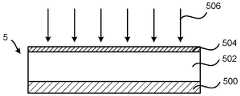
도 2는 본 발명의 실시형태에 따른 기판을 프로세싱하기 위한 프로세스 흐름도이다. 도 3a 내지 도 3d를 다시 참조하면, 프로세스 흐름(2)은 200에서 층(300) 상에 금속 산화물 필름(302)을 포함하는 기판(3)을 제공하는 단계를 포함한다. 예컨대, 금속 산화물 필름(302)은 Al2O3, HfO2, TiO2, ZrO2, Y2O3, La2O3, UO2, Lu2O3, Ta2O5, Nb2O5, ZnO, MgO, CaO, BeO, V2O5, FeO, FeO2, CrO, Cr2O3, CrO2, MnO, Mn2O3, RuO, CoO, WO3, 및 이들의 조합물로 구성된 그룹으로부터 선택될 수 있다. 202에서, 기판(3)은 금속 산화물 필름(302) 상의 플루오르화 표면 층(304)을 형성하기 위해 HF 가스(306)에 노출된다. 204에서, 기판(3)은 불활성 가스(예컨대, 아르곤(Ar) 또는 질소(N2))로 퍼징되어(purged) 초과의 HF 및 반응 부산물들을 제거할 수 있다. 206에서, 기판(3)은 플루오르화 표면 층(304)과 반응하고 플루오르화 표면 층(304)을 제거하기 위해 붕소 함유 가스(308)에 노출된다. 반응 부산물들은 기판(3)으로부터 탈착되고 프로세스 챔버 밖으로 효율적으로 펌핑되는 금속 함유 종 및 휘발성 BF3 종을 포함한다. 본 발명자들은 플루오르화 표면 종들과 조합된 붕소 함유 가스(308)의 사용이 유리하게는 플라즈마의 부재 하에서 저온 열적 ALE를 허용한다는 것을 발견했다. 붕소 함유 가스(308)는 붕소 하이드라이드(boron hydride), 붕소 할라이드(boron halide), 붕소 아미드(boron amide), 유기 붕화물(organo boride) 또는 이들의 조합물을 함유할 수 있다. 붕소 함유 가스(308)는 BH3, BCl3, B(CH3)3, 및 B(N(CH3)2)3로 구성된 그룹으로부터 선택될 수 있다. 208에서, 기판(200)은 초과의 붕소 함유 가스 및 반응 부산물들을 제거하기 위해 불활성 가스로 퍼징될(purged) 수 있다. 프로세스 화살표 210으로 나타낸 바와 같이, 금속 산화물 필름(302)을 추가로 에칭하기 위해 적어도 1회 교번 노출(202 - 208)이 반복될 수 있다. 교번 노출(202 - 208)은 하나의 ALE 사이클을 구성한다.2 is a process flow chart for processing a substrate according to an embodiment of the present invention. Referring again to FIGS. 3A-3D,
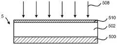
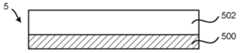
도 4는 본 발명의 실시형태에 따른 기판을 프로세싱하기 위한 프로세스 흐름도이다. 도 5a 내지 도 5f를 다시 참조하면, 프로세스 흐름(4)은 400에서 제1 플루오르화 표면 층(504)을 가진 금속 산화물 필름(502)을 포함하는 기판(5)을 제공하는 단계를 포함한다. 예컨대, 금속 산화물 필름(502)은 Al2O3, HfO2, TiO2, ZrO2, Y2O3, La2O3, UO2, Lu2O3, Ta2O5, Nb2O5, ZnO, MgO, CaO, BeO, V2O5, FeO, FeO2, CrO, Cr2O3, CrO2, MnO, Mn2O3, RuO, CoO, WO3, 및 이들의 조합물로 구성된 그룹으로부터 선택될 수 있다. 제1 플루오르화 표면 층(504)은 습식 프로세싱(예컨대, 수성 HF를 사용) 또는 건식 프로세싱(예컨대, HF 가스를 사용)에 의해 형성될 수 있다. 일 실시예에서, 제1 플루오르화 표면 층(504)은 유기 불소 함유 에칭 가스를 이용하는 에칭 프로세스에 의해 형성될 수 있다. 402에서, 기판(5)은 금속 산화물 필름(502)으로부터 제1 플루오르화 표면 층(504)을 제거하기 위해 제1 붕소 함유 가스(506)에 노출된다. 404에서, 기판(5)은 초과의 제1 붕소 함유 가스 및 반응 부산물들을 제거하기 위해 불활성 가스로 퍼징될(purged) 수 있다. 406에서, 기판(5)은 금속 산화물 필름(502) 상의 제2 플루오르화 표면 층(510)을 형성하기 위해 HF 가스(508)에 노출된다. 408에서, 기판(5)은 초과의 HF 가스 및 반응 부산물들을 제거하기 위해 불활성 가스로 퍼징될(purged) 수 있다. 410에서, 기판(500)은 금속 산화물 필름(502)으로부터 제2 플루오르화 표면 층(510)을 제거하기 위해 제2 붕소 함유 가스(512)에 노출된다.4 is a process flow diagram for processing a substrate according to an embodiment of the present invention. Referring again to FIGS. 5A-5F,
제1 및 제2 붕소 함유 가스(506 및 512)는 붕소 하이드라이드(boron hydride), 붕소 할라이드(boron halide), 붕소 아미드(boron amide), 유기 붕화물(organo boride) 또는 이들의 조합물을 함유할 수 있다. 제1 및 제2 붕소 함유 가스(506 및 512)는 BH3, BCl3, B(CH3)3, 및 B(N(CH3)2)3로 구성된 그룹으로부터 독립적으로 선택될 수 있다. 프로세스 화살표 412로 나타낸 바와 같이, 금속 산화물 필름(502)을 추가로 에칭하기 위해 적어도 1회 노출(404 - 410)이 반복될 수 있다.The first and second boron-containing
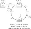
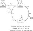
도 6은 본 발명의 실시형태에 따른 기판을 프로세싱하기 위한 프로세스 흐름도이다. 프로세스 흐름은 HF 가스와 BH3 가스의 교번 노출을 이용하여 Al2O3의 예시적 ALE를 위한 반반응 및 전반응을 나타낸다. 반응 부산물들은 기판으로부터 탈착되고 프로세스 챔버 밖으로 효율적으로 펌핑되는 H2O 종, AlH3 종, 및 휘발성 BF3 종을 포함한다.6 is a process flow chart for processing a substrate according to an embodiment of the present invention. The process flow shows the half-reaction and pre-reaction for exemplary ALE of Al2 O3 using alternating exposure of HF gas and BH3 gas. The reaction byproducts include H2 O species, AlH3 species, and volatile BF3 species that desorb from the substrate and are efficiently pumped out of the process chamber.
도 7은 본 발명의 실시형태에 따른 기판을 프로세싱하기 위한 프로세스 흐름도이다. 프로세스 흐름은 HF 가스와 BH3 가스의 교번 노출을 이용하여 Al2O3의 예시적 ALE를 위한 반반응 및 전반응을 나타내고, L은 수소, 할로겐, 아미드, 또는 유기 그룹(organic group)을 포함할 수 있다. BL3의 예는 BH3, BCl3, B(CH3)3, 및 B(N(CH3)2)3을 포함한다. 반응 부산물들은 기판으로부터 탈착되고 프로세스 챔버 밖으로 효율적으로 펌핑되는 H2O 종, AlL3 종, 및 휘발성 BF3 종을 포함한다.7 is a process flow chart for processing a substrate according to an embodiment of the present invention. The process flow represents the half-reaction and pre-reaction for exemplary ALE of Al2 O3 using alternating exposure of HF gas and BH3 gas, and L comprises hydrogen, halogen, amide, or organic group can do. Examples of BL3 include BH3 , BCl3 , B (CH3 )3 , and B (N (CH3 )2 )3 . The reaction byproducts include H2 O species, AlL3 species, and volatile BF3 species that desorb from the substrate and are efficiently pumped out of the process chamber.
붕소 함유 가스 및 HF 가스를 이용하는 원자 층 에칭을 위한 복수의 실시형태들을 설명하였다. 본 발명의 실시형태들의 상기 설명은 예시 및 설명을 위해 제시되었다. 상기 설명은 본 발명을 총망라하는 것 또는 개시된 정확한 형태에 본 발명을 제한하는 것을 의도하지 않는다. 이 설명과 후술되는 청구범위는 설명만을 목적으로 사용되고 제한으로 간주되지 않는 용어들을 포함한다. 관련 기술 분야의 당업자는 상기 교시에 비추어 많은 수정 및 변형이 가능함을 알 수 있다. 따라서, 본 발명의 범위는 이 상세한 설명에 의해서가 아니라 오히려 본 명세서에 첨부된 청구항들에 의해 제한되는 것으로 의도된다.A plurality of embodiments for atomic layer etching using boron-containing gas and HF gas have been described. The foregoing description of the embodiments of the present invention has been presented for purposes of illustration and description. The foregoing description is not intended to be exhaustive or to limit the invention to the precise form disclosed. This description and the claims that follow are intended to be illustrative only and include terms which are not to be considered as limitations. Those skilled in the art will appreciate that many modifications and variations are possible in light of the above teachings. Accordingly, the scope of the present invention is intended to be limited not by this detailed description, but rather by the claims appended hereto.
Claims (20)
Translated fromKorean기판을 제공하는 단계; 및
상기 기판을 에칭하기 위해 HF(hydrogen fluoride) 가스 및 붕소 함유 가스에 상기 기판을 노출시키는 단계
를 포함하는 원자 층 에칭(ALE)의 방법.In a method of atomic layer etching (ALE)
Providing a substrate; And
Exposing the substrate to a hydrogen fluoride (HF) gas and a boron-containing gas to etch the substrate
(ALE). ≪ / RTI >
상기 기판을 추가적으로 에칭하기 위해 교번 노출(alternating exposure)들이 적어도 1회 반복되는 것인 원자 층 에칭(ALE)의 방법.The method according to claim 1,
Wherein alternating exposures are repeated at least once to further etch the substrate. ≪ RTI ID = 0.0 > A < / RTI >
상기 붕소 함유 가스는 붕소 하이드라이드(boron hydride), 붕소 할라이드(boron halide), 붕소 아미드(boron amide), 유기 붕화물(organo boride) 또는 이들의 조합물을 함유하는 것인 원자 층 에칭(ALE)의 방법.The method according to claim 1,
Wherein the boron-containing gas comprises atomic layer etching (ALE), wherein the boron-containing gas comprises boron hydride, boron halide, boron amide, organo boride, Gt;
상기 붕소 함유 가스는 BH3, BCl3, B(CH3)3, 및 B(N(CH3)2)3로 구성된 그룹으로부터 선택되는 것인 원자 층 에칭(ALE)의 방법.The method of claim 3,
Wherein the boron-containing gas is selected from the group consisting of BH3 , BCl3 , B (CH3 )3 , and B (N (CH3 )2 )3 .
금속 산화물 필름을 포함하는 기판을 제공하는 단계;
상기 금속 산화물 필름 상의 플루오르화 표면 층을 형성하기 위해 HF 가스에 상기 기판을 노출시키는 단계; 및
상기 금속 산화물 필름으로부터 상기 플루오르화 표면 층을 제거하기 위해 붕소 함유 가스에 상기 기판을 노출시키는 단계
를 포함하는 원자 층 에칭(ALE)의 방법.In the method of atomic layer etching (ALE)
Providing a substrate comprising a metal oxide film;
Exposing the substrate to HF gas to form a fluorinated surface layer on the metal oxide film; And
Exposing the substrate to a boron-containing gas to remove the fluorinated surface layer from the metal oxide film
(ALE). ≪ / RTI >
상기 금속 산화물 필름을 추가적으로 에칭하기 위해 상기 노출이 적어도 1회 반복되는 것인 원자 층 에칭(ALE)의 방법.6. The method of claim 5,
Wherein the exposure is repeated at least once to further etch the metal oxide film.
상기 붕소 함유 가스는 붕소 하이드라이드, 붕소 할라이드, 붕소 아미드, 유기 붕화물 또는 이들의 조합물을 함유하는 것인 원자 층 에칭(ALE)의 방법.6. The method of claim 5,
Wherein the boron-containing gas comprises boron hydride, boron halide, boron amide, organic boride, or a combination thereof.
상기 붕소 함유 가스는 BH3, BCl3, B(CH3)3, 및 B(N(CH3)2)3로 구성된 그룹으로부터 선택되는 것인 원자 층 에칭(ALE)의 방법.8. The method of claim 7,
Wherein the boron-containing gas is selected from the group consisting of BH3 , BCl3 , B (CH3 )3 , and B (N (CH3 )2 )3 .
상기 금속 산화물 필름은 Al2O3, HfO2, TiO2, ZrO2, Y2O3, La2O3, UO2, Lu2O3, Ta2O5, Nb2O5, ZnO, MgO, CaO, BeO, V2O5, FeO, FeO2, CrO, Cr2O3, CrO2, MnO, Mn2O3, RuO, CoO, WO3, 및 이들의 조합물로 구성된 그룹으로부터 선택되는 것인 원자 층 에칭(ALE)의 방법.6. The method of claim 5,
The metal oxide film may be a metal oxide film such as Al2 O3 , HfO2 , TiO2 , ZrO2 , Y2 O3 , La2 O3 , UO2 , Lu2 O3 , Ta2 O5 , Nb2 O5 ,, CaO, BeO, V 2 O 5, FeO, FeO 2, CrO, Cr 2 O 3, CrO 2, MnO, Mn 2 O 3, RuO, CoO, WO 3, and that is selected from the group consisting of a combination thereof Lt; RTI ID = 0.0 > (ALE). ≪ / RTI >
상기 노출 단계들 사이에 불활성 가스로 가스 퍼징(gas purging)하는 단계를 더 포함하는 원자 층 에칭(ALE)의 방법.6. The method of claim 5,
Further comprising gas purging with an inert gas between said exposing steps. ≪ RTI ID = 0.0 > A < / RTI >
제1 플루오르화 표면 층을 가진 금속 산화물 필름을 포함하는 기판을 제공하는 단계;
상기 금속 산화물 필름으로부터 상기 제1 플루오르화 표면 층을 제거하기 위해 제1 붕소 함유 가스에 상기 기판을 노출시키는 단계;
상기 금속 산화물 필름 상의 제2 플루오르화 표면 층을 형성하기 위해 HF 가스에 상기 기판을 노출시키는 단계; 및
상기 금속 산화물 필름으로부터 상기 제2 플루오르화 표면 층을 제거하기 위해 제2 붕소 함유 가스에 상기 기판을 노출시키는 단계
를 포함하는 원자 층 에칭(ALE)의 방법.In the method of atomic layer etching (ALE)
Providing a substrate comprising a metal oxide film having a first fluorinated surface layer;
Exposing the substrate to a first boron-containing gas to remove the first fluorinated surface layer from the metal oxide film;
Exposing the substrate to HF gas to form a second fluorinated surface layer on the metal oxide film; And
Exposing the substrate to a second boron-containing gas to remove the second fluorinated surface layer from the metal oxide film
(ALE). ≪ / RTI >
상기 금속 산화물 필름을 추가적으로 에칭하기 위해 상기 HF 가스 및 상기 제2 붕소 함유 가스에 대한 노출이 적어도 1회 반복되는 것인 원자 층 에칭(ALE)의 방법.12. The method of claim 11,
Wherein the exposure to the HF gas and the second boron-containing gas is repeated at least once to further etch the metal oxide film.
상기 제1 및 제2 붕소 함유 가스는 붕소 하이드라이드, 붕소 할라이드, 붕소 아미드, 유기 붕화물 또는 이들의 조합물을 함유하는 것인 원자 층 에칭(ALE)의 방법.12. The method of claim 11,
Wherein the first and second boron-containing gases contain boron hydride, a boron halide, a boron amide, an organic boron, or a combination thereof.
상기 제1 및 제2 붕소 함유 가스는 BH3, BCl3, B(CH3)3, 및 B(N(CH3)2)3로 구성된 그룹으로부터 선택되는 것인 원자 층 에칭(ALE)의 방법.14. The method of claim 13,
Wherein the first and second boron-containing gases are selected from the group consisting of BH3 , BCl3 , B (CH3 )3 and B (N (CH3 )2 )3 . .
상기 금속 산화물 필름은 Al2O3, HfO2, TiO2, ZrO2, Y2O3, La2O3, UO2, Lu2O3, Ta2O5, Nb2O5, ZnO, MgO, CaO, BeO, V2O5, FeO, FeO2, CrO, Cr2O3, CrO2, MnO, Mn2O3, RuO, CoO, WO3, 및 이들의 조합물로 구성된 그룹으로부터 선택되는 것인 원자 층 에칭(ALE)의 방법.12. The method of claim 11,
The metal oxide filmAl 2 O 3, HfO 2, TiO 2, ZrO 2, Y 2 O 3, La 2 O 3, UO 2, Lu 2 O 3, Ta 2 O 5, Nb 2 O 5, ZnO, MgO, CaO, BeO, V 2 O 5, FeO, FeO 2, CrO, Cr 2 O 3, CrO 2, MnO, Mn 2 O 3, RuO, CoO, WO 3, and that is selected from the group consisting of a combination thereof Lt; RTI ID = 0.0 > (ALE). ≪ / RTI >
상기 금속 산화물 필름은 금속 층을 산화시킴으로써 형성되는 것인 원자 층 에칭(ALE)의 방법.12. The method of claim 11,
Wherein the metal oxide film is formed by oxidizing a metal layer.
상기 노출 단계들 사이에 불활성 가스로 가스 퍼징하는 단계를 더 포함하는 원자 층 에칭(ALE)의 방법.12. The method of claim 11,
Further comprising gas purging with an inert gas between said exposing steps. ≪ RTI ID = 0.0 > A < / RTI >
상기 제1 플루오르화 표면 층은 수성 HF에 의한 습식 프로세싱을 이용하여 형성되는 것인 원자 층 에칭(ALE)의 방법.12. The method of claim 11,
Wherein the first fluorinated surface layer is formed using wet processing with aqueous HF.
상기 제1 플루오르화 표면 층은 건식 프로세싱에 의해 형성되는 것인 원자 층 에칭(ALE)의 방법.12. The method of claim 11,
Wherein the first fluorinated surface layer is formed by dry processing.
상기 건식 프로세싱은 HF 가스 또는 유기 불소 함유 에칭 가스를 포함하는 것인 원자 층 에칭(ALE)의 방법.20. The method of claim 19,
Wherein the dry processing comprises an HF gas or an organic fluorine containing etch gas.
Applications Claiming Priority (2)
| Application Number | Priority Date | Filing Date | Title |
|---|---|---|---|
| US201662373232P | 2016-08-10 | 2016-08-10 | |
| US62/373,232 | 2016-08-10 |
Publications (2)
| Publication Number | Publication Date |
|---|---|
| KR20180018413Atrue KR20180018413A (en) | 2018-02-21 |
| KR102510736B1 KR102510736B1 (en) | 2023-03-15 |
Family
ID=61159322
Family Applications (1)
| Application Number | Title | Priority Date | Filing Date |
|---|---|---|---|
| KR1020170101457AActiveKR102510736B1 (en) | 2016-08-10 | 2017-08-10 | Atomic layer etching using a boron-containing gas and hydrogen fluoride gas |
Country Status (4)
| Country | Link |
|---|---|
| US (2) | US10283369B2 (en) |
| JP (1) | JP6924648B2 (en) |
| KR (1) | KR102510736B1 (en) |
| TW (1) | TWI717544B (en) |
Cited By (7)
| Publication number | Priority date | Publication date | Assignee | Title |
|---|---|---|---|---|
| KR20200038854A (en)* | 2018-10-04 | 2020-04-14 | 도쿄엘렉트론가부시키가이샤 | Surface processing method and processing system |
| KR20200103471A (en)* | 2019-02-25 | 2020-09-02 | 주식회사 아이큐랩 | METHOD FOR FABRICATING TRENCH IN SiC SEMICONDUCTOR PROCESS |
| KR20220004014A (en)* | 2020-06-30 | 2022-01-11 | 주식회사 히타치하이테크 | Etching processing method and etching processing apparatus |
| KR20220018025A (en)* | 2019-06-11 | 2022-02-14 | 어플라이드 머티어리얼스, 인코포레이티드 | Etching of metal oxides using fluorine and metal halides |
| US11387112B2 (en) | 2018-10-04 | 2022-07-12 | Tokyo Electron Limited | Surface processing method and processing system |
| KR20230089501A (en)* | 2021-12-13 | 2023-06-20 | 한양대학교 에리카산학협력단 | Atomic layer etching method and atomic layer etching apparatus for high-k thin film |
| KR20230089500A (en)* | 2021-12-13 | 2023-06-20 | 한양대학교 에리카산학협력단 | Atomic layer etching process based on catalytic reaction |
Families Citing this family (19)
| Publication number | Priority date | Publication date | Assignee | Title |
|---|---|---|---|---|
| US10283369B2 (en)* | 2016-08-10 | 2019-05-07 | Tokyo Electron Limited | Atomic layer etching using a boron-containing gas and hydrogen fluoride gas |
| US10566212B2 (en) | 2016-12-19 | 2020-02-18 | Lam Research Corporation | Designer atomic layer etching |
| JP6679642B2 (en)* | 2018-03-27 | 2020-04-15 | 株式会社Kokusai Electric | Semiconductor device manufacturing method, substrate processing apparatus, and program |
| KR20220011212A (en) | 2018-09-13 | 2022-01-27 | 샌트랄 글래스 컴퍼니 리미티드 | Method and device for etching silicon oxide |
| CN111168056A (en)* | 2020-01-17 | 2020-05-19 | 宁波柔创纳米科技有限公司 | Metal powder and method for reducing oxygen content of metal powder and improving oxidation resistance |
| US20230104924A1 (en)* | 2020-02-18 | 2023-04-06 | Forge Nano, Inc. | Atomic Layer Deposition (ALD) for Multi-Layer Ceramic Capacitors (MLCCs) |
| JP7096279B2 (en)* | 2020-03-25 | 2022-07-05 | 株式会社Kokusai Electric | Semiconductor device manufacturing methods, board processing devices, programs, and board processing methods |
| JP7174016B2 (en) | 2020-07-16 | 2022-11-17 | 株式会社Kokusai Electric | Substrate processing method, semiconductor device manufacturing method, substrate processing apparatus, and program |
| WO2022050099A1 (en)* | 2020-09-01 | 2022-03-10 | 株式会社Adeka | Etching method |
| US11488835B2 (en) | 2020-11-20 | 2022-11-01 | Applied Materials, Inc. | Systems and methods for tungsten-containing film removal |
| JP7621876B2 (en)* | 2021-01-26 | 2025-01-27 | 東京エレクトロン株式会社 | Substrate processing method, component processing method, and substrate processing apparatus |
| US11462414B2 (en) | 2021-03-08 | 2022-10-04 | Tokyo Electron Limited | Atomic layer etching of metal oxides |
| US11631589B2 (en)* | 2021-05-04 | 2023-04-18 | Applied Materials, Inc. | Metal etch in high aspect-ratio features |
| JP7712362B2 (en) | 2021-07-05 | 2025-07-23 | 東京エレクトロン株式会社 | SUBSTRATE PROCESSING METHOD AND SUBSTRATE PROCESSING APPARATUS |
| JP2024533108A (en)* | 2021-09-07 | 2024-09-12 | ラム リサーチ コーポレーション | Atomic Layer Etching with Boron Trichloride |
| WO2023164367A1 (en)* | 2022-02-22 | 2023-08-31 | Lam Research Corporation | Atomic layer etching using an inhibitor |
| CN119137713A (en) | 2022-05-02 | 2024-12-13 | 东京毅力科创株式会社 | Plasma processing method and plasma processing device |
| JP7709946B2 (en)* | 2022-09-22 | 2025-07-17 | 株式会社Kokusai Electric | SUBSTRATE PROCESSING METHOD, SEMICONDUCTOR DEVICE MANUFACTURING METHOD, PROGRAM, AND SUBSTRATE PROCESSING APPARATUS |
| KR20250140553A (en)* | 2023-01-27 | 2025-09-25 | 도쿄엘렉트론가부시키가이샤 | Substrate processing method and substrate processing system |
Citations (6)
| Publication number | Priority date | Publication date | Assignee | Title |
|---|---|---|---|---|
| US5041362A (en)* | 1989-07-06 | 1991-08-20 | Texas Instruments Incorporated | Dry developable resist etch chemistry |
| JPH09246581A (en)* | 1996-03-01 | 1997-09-19 | Canon Inc | Photovoltaic element |
| US7012027B2 (en)* | 2004-01-27 | 2006-03-14 | Taiwan Semiconductor Manufacturing Company, Ltd. | Zirconium oxide and hafnium oxide etching using halogen containing chemicals |
| US20140179106A1 (en)* | 2012-12-21 | 2014-06-26 | Lam Research Corporation | In-situ metal residue clean |
| US20150270140A1 (en)* | 2014-06-09 | 2015-09-24 | American Air Liquide, Inc. | Atomic layer or cyclic plasma etching chemistries and processes |
| WO2016100873A1 (en)* | 2014-12-18 | 2016-06-23 | The Regents Of The University Of Colorado, A Body Corporate | Novel methods of atomic layer etching (ale) using sequential, self-limiting thermal reactions |
Family Cites Families (5)
| Publication number | Priority date | Publication date | Assignee | Title |
|---|---|---|---|---|
| DE68923247T2 (en)* | 1988-11-04 | 1995-10-26 | Fujitsu Ltd | Process for producing a photoresist pattern. |
| JP5297615B2 (en)* | 2007-09-07 | 2013-09-25 | 株式会社日立ハイテクノロジーズ | Dry etching method |
| US9576811B2 (en)* | 2015-01-12 | 2017-02-21 | Lam Research Corporation | Integrating atomic scale processes: ALD (atomic layer deposition) and ALE (atomic layer etch) |
| US9837304B2 (en)* | 2015-06-24 | 2017-12-05 | Tokyo Electron Limited | Sidewall protection scheme for contact formation |
| US10283369B2 (en)* | 2016-08-10 | 2019-05-07 | Tokyo Electron Limited | Atomic layer etching using a boron-containing gas and hydrogen fluoride gas |
- 2017
- 2017-08-08USUS15/671,404patent/US10283369B2/enactiveActive
- 2017-08-09TWTW106126861Apatent/TWI717544B/enactive
- 2017-08-09JPJP2017154337Apatent/JP6924648B2/enactiveActive
- 2017-08-10KRKR1020170101457Apatent/KR102510736B1/enactiveActive
- 2019
- 2019-05-07USUS16/405,462patent/US10790156B2/enactiveActive
Patent Citations (6)
| Publication number | Priority date | Publication date | Assignee | Title |
|---|---|---|---|---|
| US5041362A (en)* | 1989-07-06 | 1991-08-20 | Texas Instruments Incorporated | Dry developable resist etch chemistry |
| JPH09246581A (en)* | 1996-03-01 | 1997-09-19 | Canon Inc | Photovoltaic element |
| US7012027B2 (en)* | 2004-01-27 | 2006-03-14 | Taiwan Semiconductor Manufacturing Company, Ltd. | Zirconium oxide and hafnium oxide etching using halogen containing chemicals |
| US20140179106A1 (en)* | 2012-12-21 | 2014-06-26 | Lam Research Corporation | In-situ metal residue clean |
| US20150270140A1 (en)* | 2014-06-09 | 2015-09-24 | American Air Liquide, Inc. | Atomic layer or cyclic plasma etching chemistries and processes |
| WO2016100873A1 (en)* | 2014-12-18 | 2016-06-23 | The Regents Of The University Of Colorado, A Body Corporate | Novel methods of atomic layer etching (ale) using sequential, self-limiting thermal reactions |
Cited By (8)
| Publication number | Priority date | Publication date | Assignee | Title |
|---|---|---|---|---|
| KR20200038854A (en)* | 2018-10-04 | 2020-04-14 | 도쿄엘렉트론가부시키가이샤 | Surface processing method and processing system |
| US11387112B2 (en) | 2018-10-04 | 2022-07-12 | Tokyo Electron Limited | Surface processing method and processing system |
| KR20200103471A (en)* | 2019-02-25 | 2020-09-02 | 주식회사 아이큐랩 | METHOD FOR FABRICATING TRENCH IN SiC SEMICONDUCTOR PROCESS |
| KR20220018025A (en)* | 2019-06-11 | 2022-02-14 | 어플라이드 머티어리얼스, 인코포레이티드 | Etching of metal oxides using fluorine and metal halides |
| KR20220004014A (en)* | 2020-06-30 | 2022-01-11 | 주식회사 히타치하이테크 | Etching processing method and etching processing apparatus |
| US11901192B2 (en) | 2020-06-30 | 2024-02-13 | Hitachi High-Tech Corporation | Etching processing method and etching processing apparatus |
| KR20230089501A (en)* | 2021-12-13 | 2023-06-20 | 한양대학교 에리카산학협력단 | Atomic layer etching method and atomic layer etching apparatus for high-k thin film |
| KR20230089500A (en)* | 2021-12-13 | 2023-06-20 | 한양대학교 에리카산학협력단 | Atomic layer etching process based on catalytic reaction |
Also Published As
| Publication number | Publication date |
|---|---|
| US20190267249A1 (en) | 2019-08-29 |
| US20180047577A1 (en) | 2018-02-15 |
| KR102510736B1 (en) | 2023-03-15 |
| JP2018026566A (en) | 2018-02-15 |
| TW201820459A (en) | 2018-06-01 |
| JP6924648B2 (en) | 2021-08-25 |
| US10283369B2 (en) | 2019-05-07 |
| US10790156B2 (en) | 2020-09-29 |
| TWI717544B (en) | 2021-02-01 |
Similar Documents
| Publication | Publication Date | Title |
|---|---|---|
| KR102510736B1 (en) | Atomic layer etching using a boron-containing gas and hydrogen fluoride gas | |
| JP2018026566A5 (en) | ||
| CN110313054B (en) | Self-limiting atomic thermal etch system and method | |
| US9911607B2 (en) | Method of processing target object | |
| JP6785219B2 (en) | How to form a superconducting wiring layer with low magnetic noise | |
| TWI815325B (en) | 3d nand etch | |
| KR20190040313A (en) | Pseudo-atomic layer etching method | |
| US10381236B2 (en) | Method of processing target object | |
| KR20170102429A (en) | ATOMIC LAYER ETCHING OF Al2O3 USING A COMBINATION OF PLASMA AND VAPOR TREATMENTS | |
| US10553446B2 (en) | Method of processing target object | |
| US11658037B2 (en) | Method of atomic layer etching of oxide | |
| TWI883379B (en) | Etching of metal oxides using fluorine and metal halides | |
| JP6537473B2 (en) | Method of processing an object | |
| TW201738952A (en) | Method and system for atomic layer etching | |
| US10707088B2 (en) | Method of processing target object | |
| JP2010225899A (en) | Method of manufacturing semiconductor device | |
| KR101998844B1 (en) | Semiconductor device fabrication using etch stop layer | |
| KR20210149901A (en) | Treatments to improve material structures | |
| JP5075897B2 (en) | Manufacturing method of semiconductor device | |
| CN105632908B (en) | Method for forming semiconductor structure | |
| KR102693152B1 (en) | Atomic Layer Etching using self-limiting reaction | |
| CN102779748B (en) | The manufacture method of semiconductor device | |
| US20240087893A1 (en) | Methods for forming mandrels and spacers, related structures, and systems | |
| KR20230089500A (en) | Atomic layer etching process based on catalytic reaction | |
| JP2010509776A (en) | Removable spacer |
Legal Events
| Date | Code | Title | Description |
|---|---|---|---|
| PA0109 | Patent application | Patent event code:PA01091R01D Comment text:Patent Application Patent event date:20170810 | |
| PG1501 | Laying open of application | ||
| A201 | Request for examination | ||
| PA0201 | Request for examination | Patent event code:PA02012R01D Patent event date:20200805 Comment text:Request for Examination of Application Patent event code:PA02011R01I Patent event date:20170810 Comment text:Patent Application | |
| E902 | Notification of reason for refusal | ||
| PE0902 | Notice of grounds for rejection | Comment text:Notification of reason for refusal Patent event date:20220530 Patent event code:PE09021S01D | |
| E701 | Decision to grant or registration of patent right | ||
| PE0701 | Decision of registration | Patent event code:PE07011S01D Comment text:Decision to Grant Registration Patent event date:20221226 | |
| GRNT | Written decision to grant | ||
| PR0701 | Registration of establishment | Comment text:Registration of Establishment Patent event date:20230313 Patent event code:PR07011E01D | |
| PR1002 | Payment of registration fee | Payment date:20230313 End annual number:3 Start annual number:1 | |
| PG1601 | Publication of registration |