KR20180017077A - Iridium complexes, light-emitting devices, display devices, electronic devices, and lighting devices - Google Patents
Iridium complexes, light-emitting devices, display devices, electronic devices, and lighting devicesDownload PDFInfo
- Publication number
- KR20180017077A KR20180017077AKR1020187000237AKR20187000237AKR20180017077AKR 20180017077 AKR20180017077 AKR 20180017077AKR 1020187000237 AKR1020187000237 AKR 1020187000237AKR 20187000237 AKR20187000237 AKR 20187000237AKR 20180017077 AKR20180017077 AKR 20180017077A
- Authority
- KR
- South Korea
- Prior art keywords
- group
- carbon atoms
- organic compound
- light emitting
- guest material
- Prior art date
- Legal status (The legal status is an assumption and is not a legal conclusion. Google has not performed a legal analysis and makes no representation as to the accuracy of the status listed.)
- Ceased
Links
- BMFBAHYERSPMLT-UHFFFAOYSA-NBc1cc(C#N)ccc1CChemical compoundBc1cc(C#N)ccc1CBMFBAHYERSPMLT-UHFFFAOYSA-N0.000description1
- PFNCYDZSYCPYSJ-UHFFFAOYSA-NCc(nc1-c2cc(-c3c(C)ccc(C#N)c3)ccc2)n[n]1-c1c(C)cc(C)cc1CChemical compoundCc(nc1-c2cc(-c3c(C)ccc(C#N)c3)ccc2)n[n]1-c1c(C)cc(C)cc1CPFNCYDZSYCPYSJ-UHFFFAOYSA-N0.000description1
- NYLILSNMAIGTRW-UHFFFAOYSA-NCc(nc1-c2cc(Br)ccc2)n[n]1-c1c(C)cc(C)cc1CChemical compoundCc(nc1-c2cc(Br)ccc2)n[n]1-c1c(C)cc(C)cc1CNYLILSNMAIGTRW-UHFFFAOYSA-N0.000description1
Images


Classifications
- H—ELECTRICITY
- H10—SEMICONDUCTOR DEVICES; ELECTRIC SOLID-STATE DEVICES NOT OTHERWISE PROVIDED FOR
- H10K—ORGANIC ELECTRIC SOLID-STATE DEVICES
- H10K85/00—Organic materials used in the body or electrodes of devices covered by this subclass
- H10K85/30—Coordination compounds
- H10K85/341—Transition metal complexes, e.g. Ru(II)polypyridine complexes
- H10K85/342—Transition metal complexes, e.g. Ru(II)polypyridine complexes comprising iridium
- C—CHEMISTRY; METALLURGY
- C07—ORGANIC CHEMISTRY
- C07F—ACYCLIC, CARBOCYCLIC OR HETEROCYCLIC COMPOUNDS CONTAINING ELEMENTS OTHER THAN CARBON, HYDROGEN, HALOGEN, OXYGEN, NITROGEN, SULFUR, SELENIUM OR TELLURIUM
- C07F15/00—Compounds containing elements of Groups 8, 9, 10 or 18 of the Periodic Table
- C07F15/0006—Compounds containing elements of Groups 8, 9, 10 or 18 of the Periodic Table compounds of the platinum group
- C07F15/0033—Iridium compounds
- C—CHEMISTRY; METALLURGY
- C09—DYES; PAINTS; POLISHES; NATURAL RESINS; ADHESIVES; COMPOSITIONS NOT OTHERWISE PROVIDED FOR; APPLICATIONS OF MATERIALS NOT OTHERWISE PROVIDED FOR
- C09K—MATERIALS FOR MISCELLANEOUS APPLICATIONS, NOT PROVIDED FOR ELSEWHERE
- C09K11/00—Luminescent, e.g. electroluminescent, chemiluminescent materials
- C09K11/02—Use of particular materials as binders, particle coatings or suspension media therefor
- C09K11/025—Use of particular materials as binders, particle coatings or suspension media therefor non-luminescent particle coatings or suspension media
- C—CHEMISTRY; METALLURGY
- C09—DYES; PAINTS; POLISHES; NATURAL RESINS; ADHESIVES; COMPOSITIONS NOT OTHERWISE PROVIDED FOR; APPLICATIONS OF MATERIALS NOT OTHERWISE PROVIDED FOR
- C09K—MATERIALS FOR MISCELLANEOUS APPLICATIONS, NOT PROVIDED FOR ELSEWHERE
- C09K11/00—Luminescent, e.g. electroluminescent, chemiluminescent materials
- C09K11/06—Luminescent, e.g. electroluminescent, chemiluminescent materials containing organic luminescent materials
- H01L27/322—
- H01L27/323—
- H01L27/3262—
- H01L51/0085—
- H01L51/5004—
- H01L51/5028—
- H—ELECTRICITY
- H10—SEMICONDUCTOR DEVICES; ELECTRIC SOLID-STATE DEVICES NOT OTHERWISE PROVIDED FOR
- H10K—ORGANIC ELECTRIC SOLID-STATE DEVICES
- H10K50/00—Organic light-emitting devices
- H10K50/10—OLEDs or polymer light-emitting diodes [PLED]
- H10K50/11—OLEDs or polymer light-emitting diodes [PLED] characterised by the electroluminescent [EL] layers
- H—ELECTRICITY
- H10—SEMICONDUCTOR DEVICES; ELECTRIC SOLID-STATE DEVICES NOT OTHERWISE PROVIDED FOR
- H10K—ORGANIC ELECTRIC SOLID-STATE DEVICES
- H10K59/00—Integrated devices, or assemblies of multiple devices, comprising at least one organic light-emitting element covered by group H10K50/00
- C—CHEMISTRY; METALLURGY
- C09—DYES; PAINTS; POLISHES; NATURAL RESINS; ADHESIVES; COMPOSITIONS NOT OTHERWISE PROVIDED FOR; APPLICATIONS OF MATERIALS NOT OTHERWISE PROVIDED FOR
- C09K—MATERIALS FOR MISCELLANEOUS APPLICATIONS, NOT PROVIDED FOR ELSEWHERE
- C09K2211/00—Chemical nature of organic luminescent or tenebrescent compounds
- C09K2211/10—Non-macromolecular compounds
- C09K2211/1003—Carbocyclic compounds
- C09K2211/1007—Non-condensed systems
- C—CHEMISTRY; METALLURGY
- C09—DYES; PAINTS; POLISHES; NATURAL RESINS; ADHESIVES; COMPOSITIONS NOT OTHERWISE PROVIDED FOR; APPLICATIONS OF MATERIALS NOT OTHERWISE PROVIDED FOR
- C09K—MATERIALS FOR MISCELLANEOUS APPLICATIONS, NOT PROVIDED FOR ELSEWHERE
- C09K2211/00—Chemical nature of organic luminescent or tenebrescent compounds
- C09K2211/10—Non-macromolecular compounds
- C09K2211/1018—Heterocyclic compounds
- C09K2211/1025—Heterocyclic compounds characterised by ligands
- C09K2211/1059—Heterocyclic compounds characterised by ligands containing three nitrogen atoms as heteroatoms
- C—CHEMISTRY; METALLURGY
- C09—DYES; PAINTS; POLISHES; NATURAL RESINS; ADHESIVES; COMPOSITIONS NOT OTHERWISE PROVIDED FOR; APPLICATIONS OF MATERIALS NOT OTHERWISE PROVIDED FOR
- C09K—MATERIALS FOR MISCELLANEOUS APPLICATIONS, NOT PROVIDED FOR ELSEWHERE
- C09K2211/00—Chemical nature of organic luminescent or tenebrescent compounds
- C09K2211/18—Metal complexes
- C09K2211/185—Metal complexes of the platinum group, i.e. Os, Ir, Pt, Ru, Rh or Pd
- H—ELECTRICITY
- H10—SEMICONDUCTOR DEVICES; ELECTRIC SOLID-STATE DEVICES NOT OTHERWISE PROVIDED FOR
- H10K—ORGANIC ELECTRIC SOLID-STATE DEVICES
- H10K2101/00—Properties of the organic materials covered by group H10K85/00
- H10K2101/10—Triplet emission
- H—ELECTRICITY
- H10—SEMICONDUCTOR DEVICES; ELECTRIC SOLID-STATE DEVICES NOT OTHERWISE PROVIDED FOR
- H10K—ORGANIC ELECTRIC SOLID-STATE DEVICES
- H10K2101/00—Properties of the organic materials covered by group H10K85/00
- H10K2101/20—Delayed fluorescence emission
- H10K2101/25—Delayed fluorescence emission using exciplex
- H—ELECTRICITY
- H10—SEMICONDUCTOR DEVICES; ELECTRIC SOLID-STATE DEVICES NOT OTHERWISE PROVIDED FOR
- H10K—ORGANIC ELECTRIC SOLID-STATE DEVICES
- H10K2101/00—Properties of the organic materials covered by group H10K85/00
- H10K2101/30—Highest occupied molecular orbital [HOMO], lowest unoccupied molecular orbital [LUMO] or Fermi energy values
- H—ELECTRICITY
- H10—SEMICONDUCTOR DEVICES; ELECTRIC SOLID-STATE DEVICES NOT OTHERWISE PROVIDED FOR
- H10K—ORGANIC ELECTRIC SOLID-STATE DEVICES
- H10K2101/00—Properties of the organic materials covered by group H10K85/00
- H10K2101/40—Interrelation of parameters between multiple constituent active layers or sublayers, e.g. HOMO values in adjacent layers
- H—ELECTRICITY
- H10—SEMICONDUCTOR DEVICES; ELECTRIC SOLID-STATE DEVICES NOT OTHERWISE PROVIDED FOR
- H10K—ORGANIC ELECTRIC SOLID-STATE DEVICES
- H10K2101/00—Properties of the organic materials covered by group H10K85/00
- H10K2101/80—Composition varying spatially, e.g. having a spatial gradient
- H—ELECTRICITY
- H10—SEMICONDUCTOR DEVICES; ELECTRIC SOLID-STATE DEVICES NOT OTHERWISE PROVIDED FOR
- H10K—ORGANIC ELECTRIC SOLID-STATE DEVICES
- H10K2101/00—Properties of the organic materials covered by group H10K85/00
- H10K2101/90—Multiple hosts in the emissive layer
- H—ELECTRICITY
- H10—SEMICONDUCTOR DEVICES; ELECTRIC SOLID-STATE DEVICES NOT OTHERWISE PROVIDED FOR
- H10K—ORGANIC ELECTRIC SOLID-STATE DEVICES
- H10K85/00—Organic materials used in the body or electrodes of devices covered by this subclass
- H10K85/60—Organic compounds having low molecular weight
- H10K85/649—Aromatic compounds comprising a hetero atom
- H10K85/654—Aromatic compounds comprising a hetero atom comprising only nitrogen as heteroatom
- H—ELECTRICITY
- H10—SEMICONDUCTOR DEVICES; ELECTRIC SOLID-STATE DEVICES NOT OTHERWISE PROVIDED FOR
- H10K—ORGANIC ELECTRIC SOLID-STATE DEVICES
- H10K85/00—Organic materials used in the body or electrodes of devices covered by this subclass
- H10K85/60—Organic compounds having low molecular weight
- H10K85/649—Aromatic compounds comprising a hetero atom
- H10K85/657—Polycyclic condensed heteroaromatic hydrocarbons
- H10K85/6572—Polycyclic condensed heteroaromatic hydrocarbons comprising only nitrogen in the heteroaromatic polycondensed ring system, e.g. phenanthroline or carbazole
- H—ELECTRICITY
- H10—SEMICONDUCTOR DEVICES; ELECTRIC SOLID-STATE DEVICES NOT OTHERWISE PROVIDED FOR
- H10K—ORGANIC ELECTRIC SOLID-STATE DEVICES
- H10K85/00—Organic materials used in the body or electrodes of devices covered by this subclass
- H10K85/60—Organic compounds having low molecular weight
- H10K85/649—Aromatic compounds comprising a hetero atom
- H10K85/657—Polycyclic condensed heteroaromatic hydrocarbons
- H10K85/6576—Polycyclic condensed heteroaromatic hydrocarbons comprising only sulfur in the heteroaromatic polycondensed ring system, e.g. benzothiophene
Landscapes
- Chemical & Material Sciences (AREA)
- Organic Chemistry (AREA)
- Engineering & Computer Science (AREA)
- Materials Engineering (AREA)
- Crystallography & Structural Chemistry (AREA)
- Inorganic Chemistry (AREA)
- Physics & Mathematics (AREA)
- Optics & Photonics (AREA)
- Electroluminescent Light Sources (AREA)
- Devices For Indicating Variable Information By Combining Individual Elements (AREA)
Abstract
Translated fromKorean
Description
Translated fromKorean본 발명의 일 형태는 발광 소자, 또는 상기 발광 소자를 각각 포함하는 표시 장치, 전자 기기, 및 조명 장치에 관한 것이다.One aspect of the present invention relates to a light emitting device, or a display device, an electronic device, and a lighting device each including the light emitting device.
또한, 본 발명의 일 형태는 상술한 기술분야에 한정되지 않는다. 본 명세서 등에 개시(開示)되는 발명의 일 형태의 기술분야는 물건, 방법, 또는 제작 방법에 관한 것이다. 또한, 본 발명의 일 형태는 공정(process), 기계(machine), 제품(manufacture), 또는 조성물(composition of matter)에 관한 것이다. 구체적으로는, 본 명세서에 개시되는 본 발명의 일 형태의 기술분야의 예에는 반도체 장치, 표시 장치, 액정 표시 장치, 발광 장치, 조명 장치, 축전 장치, 기억 장치, 이들 중 어느 것의 구동 방법, 및 이들 중 어느 것의 제작 방법이 포함된다.Further, an aspect of the present invention is not limited to the above-described technical field. One technical field of the invention disclosed in this specification and the like relates to a thing, a method, or a manufacturing method. In addition, one form of the present invention relates to a process, a machine, a manufacture, or a composition of matter. Specifically, examples of the technical field of the present invention disclosed in this specification include a semiconductor device, a display device, a liquid crystal display device, a light emitting device, a lighting device, a power storage device, a storage device, And a manufacturing method of any of them.
근년, EL(electroluminescence)을 사용한 발광 소자에 대한 연구 개발이 광범위하게 진행되고 있다. 이러한 발광 소자의 기본적인 구조에서는, 발광성 물질을 포함하는 층(EL층)이 한 쌍의 전극 사이에 개재(介在)되어 있다. 이 소자의 한 쌍의 전극 사이에 전압을 인가함으로써, 발광성 물질로부터의 발광을 얻을 수 있다.BACKGROUND ART In recent years, research and development on a light emitting device using EL (electroluminescence) has been widely carried out. In the basic structure of such a light emitting element, a layer (EL layer) containing a luminescent material is interposed between a pair of electrodes. By applying a voltage between a pair of electrodes of this element, light emission from the luminescent material can be obtained.
상술한 발광 소자는 자발광형이기 때문에, 이 발광 소자를 사용한 표시 장치는 시인성이 높고, 백라이트가 불필요하고, 소비전력이 낮은 등의 이점을 갖는다. 또한, 상기 표시 장치는 얇고 가볍게 형성할 수 있고, 응답 속도가 빠르다는 이점도 갖는다.Since the above-described light-emitting element is of a self-emission type, a display device using the light-emitting element has advantages such as high visibility, no backlight, and low power consumption. Further, the display device can be formed thin and light, and has the advantage of a high response speed.
EL층이 발광성 물질로서 유기 화합물을 포함하며 한 쌍의 전극 사이에 제공되어 있는 발광 소자(예를 들어, 유기 EL 소자)에서는, 한 쌍의 전극 사이에 전압을 인가함으로써, 음극으로부터 전자가, 양극으로부터 정공이 발광성을 갖는 EL층으로 주입되어 전류가 흐른다. 주입된 전자와 정공이 재결합함으로써, 발광성을 갖는 유기 화합물이 여기 상태가 되어 발광이 얻어진다.In a light emitting element (for example, an organic EL element) in which an EL layer is provided as a luminescent material and an organic compound is provided between a pair of electrodes, by applying a voltage between the pair of electrodes, The holes are injected into the EL layer having the light emitting property, and a current flows. The recombination of the injected electrons and the holes brings the organic compound having the luminescence into the excited state, and the luminescence is obtained.
또한, 유기 화합물에 의하여 형성되는 여기 상태는 단일항 여기 상태(S*) 또는 삼중항 여기 상태(T*)일 수 있다. 단일항 여기 상태로부터의 발광을 형광이라고 하고, 삼중항 여기 상태로부터의 발광을 인광이라고 한다. 발광 소자에서의 S* 대 T*의 생성비는 1:3이다. 바꿔 말하면, 인광을 방출하는 화합물(인광성 화합물)을 포함하는 발광 소자는 형광을 방출하는 화합물(형광성 화합물)을 포함하는 발광 소자보다 발광 효율이 더 높다. 그러므로, 근년에는 삼중항 여기 상태를 발광으로 변환할 수 있는 인광성 화합물을 포함하는 발광 소자가 활발히 개발되어지고 있다(예를 들어, 특허문헌 1 참조).Further, the excited state formed by the organic compound may be a singlet excited state (S* ) or a triplet excited state (T* ). Light emission from a singlet excited state is referred to as fluorescence and light emission from a triplet excited state is referred to as phosphorescence. The generation ratio of S* to T* in the light emitting device is 1: 3. In other words, the light emitting device including the compound (phosphorescent compound) that emits phosphorescence has higher luminescence efficiency than the light emitting device including the compound that emits fluorescence (fluorescent compound). Therefore, in recent years, light emitting devices including a phosphorescent compound capable of converting a triplet excited state into light emission have been actively developed (see, for example, Patent Document 1).
유기 화합물을 여기시키기 위한 에너지는, 유기 화합물의 LUMO 준위와 HOMO 준위의 에너지 차이에 의존한다. 이 에너지 차이는 실질적으로 단일항 여기 에너지에 상당한다. 인광성 화합물을 포함하는 발광 소자에서는, 삼중항 여기 에너지가 발광 에너지로 변환된다. 따라서, 유기 화합물의 단일항 여기 에너지와 삼중항 여기 에너지의 에너지 차이가 큰 경우, 유기 화합물을 여기시키기 위한 에너지는 상기 에너지 차이만큼 발광 에너지보다 높아진다. 유기 화합물을 여기시키기 위한 에너지와 발광 에너지의 차이는, 발광 소자의 구동 전압을 상승시켜 발광 소자의 소자 특성에 영향을 미친다. 이러한 이유로, 구동 전압을 저감하기 위한 방법이 모색되고 있다(특허문헌 2 참조).The energy for exciting the organic compound depends on the energy difference between the LUMO level and the HOMO level of the organic compound. This energy difference substantially corresponds to a single anti-excitation energy. In a light-emitting device including a phosphorescent compound, triplet excitation energy is converted into light emission energy. Therefore, when the energy difference between the single excitation energy and triplet excitation energy of the organic compound is large, the energy for exciting the organic compound becomes higher than the light emission energy by the energy difference. The difference between the energy and the light emitting energy for exciting the organic compound increases the driving voltage of the light emitting element and affects the device characteristics of the light emitting element. For this reason, a method for reducing the driving voltage has been sought (see Patent Document 2).
인광성 화합물을 포함하는 발광 소자 중에서, 청색광을 방출하는 발광 소자는, 삼중항 여기 에너지 준위가 높은 안정적인 화합물의 개발이 어려운 것으로 인해 아직 실용화에 이르지 못하고 있다. 따라서, 발광 효율이 높고 안정된 인광성 화합물과, 발광 효율이 높고 신뢰성이 높은 인광 발광 소자의 개발이 요구되고 있다.Among light emitting devices including phosphorescent compounds, light emitting devices that emit blue light have not been put into practical use due to difficulty in developing stable compounds having a high triplet excitation energy level. Therefore, development of a phosphorescent compound having high and stable luminescence efficiency and a phosphorescent light emitting element having high luminescence efficiency and high reliability is required.
발광 효율이 높은 인광성 화합물로서 이리듐 착체가 알려져 있다. 발광 에너지가 높은 이리듐 착체로서, 질소 함유 5원 헤테로고리 골격을 배위자로서 포함하는 이리듐 착체가 알려져 있다. 상기 질소 함유 5원 헤테로고리 골격은 삼중항 여기 에너지가 높지만, 질소 함유 6원 헤테로고리 골격보다 전자 수용성이 낮다. 그러므로, 질소 함유 5원 헤테로고리 골격을 배위자로서 포함하는 이리듐 착체는, LUMO 준위가 높고 전자 캐리어가 쉽게 주입되지 않는다. 이러한 이유로, 질소 함유 5원 헤테로고리 골격을 배위자로서 포함하는 이리듐 착체에서는, 캐리어의 직접 재결합에 의한 여기가 어렵고, 이는 효율적인 발광이 어렵다는 것을 의미한다.An iridium complex is known as a phosphorescent compound having a high luminous efficiency. As an iridium complex having a high light emitting energy, an iridium complex containing a nitrogen-containing 5-membered heterocyclic skeleton as a ligand is known. The nitrogen-containing 5-membered heterocyclic skeleton has a high triplet excitation energy, but has a lower electron acceptance than the nitrogen-containing 6-membered heterocyclic skeleton. Therefore, an iridium complex containing a nitrogen-containing 5-membered heterocyclic skeleton as a ligand has a high LUMO level and can not easily inject an electron carrier. For this reason, in an iridium complex containing a nitrogen-containing 5-membered heterocyclic skeleton as a ligand, it is difficult to excite by direct recombination of carriers, which means that efficient luminescence is difficult.
상술한 것으로부터, 인광성 화합물을 포함하고 발광 효율이 높은 발광 소자를 제공하는 것을 본 발명의 일 형태의 과제로 한다. 소비전력이 낮은 발광 소자를 제공하는 것을 본 발명의 일 형태의 또 다른 과제로 한다. 신뢰성이 높은 발광 소자를 제공하는 것을 본 발명의 일 형태의 또 다른 과제로 한다. 신규 화합물을 제공하는 것을 본 발명의 일 형태의 또 다른 과제로 한다. 신규 화합물을 포함하는 발광 소자를 제공하는 것을 본 발명의 일 형태의 또 다른 과제로 한다. 신규 발광 소자를 제공하는 것을 본 발명의 일 형태의 또 다른 과제로 한다. 신규 발광 장치를 제공하는 것을 본 발명의 일 형태의 또 다른 과제로 한다. 신규 표시 장치를 제공하는 것을 본 발명의 일 형태의 또 다른 과제로 한다.From the above, it is an object of one aspect of the present invention to provide a light emitting device containing a phosphorescent compound and having high luminous efficiency. It is another object of one aspect of the present invention to provide a light emitting device having low power consumption. It is another object of the present invention to provide a light emitting device having high reliability. It is another object of one aspect of the present invention to provide a novel compound. It is another object of one aspect of the present invention to provide a light emitting device comprising a novel compound. It is another object of one aspect of the present invention to provide a novel light emitting device. It is another object of one aspect of the present invention to provide a novel light emitting device. It is another object of the present invention to provide a new display device.
또한, 이들 과제의 기재는 다른 과제의 존재를 방해하지 않는다. 본 발명의 일 형태에서 상기 모든 과제를 달성할 필요는 없다. 다른 과제는 명세서 등의 기재로부터 명백해질 것이며 추출될 수 있다.Further, the description of these tasks does not hinder the existence of other problems. It is not necessary to achieve all of the above-mentioned problems in one form of the present invention. Other tasks will become apparent from the description of the specification and the like and can be extracted.
본 발명의 일 형태는 인광성 화합물을 효율적으로 여기시킬 수 있는 엑시플렉스를 포함하는 발광 소자, 또는 발광 에너지가 높은 광을 방출할 수 있는 신규 인광성 화합물을 포함하는 발광 소자이다.One embodiment of the present invention is a light emitting device comprising an exciplex capable of efficiently exciting a phosphorescent compound, or a novel phosphorescent compound capable of emitting light having a high light emitting energy.
따라서, 본 발명의 일 형태는 제 1 유기 화합물, 제 2 유기 화합물, 및 게스트 재료를 포함하는 발광 소자이다. 제 1 유기 화합물의 LUMO 준위는 제 2 유기 화합물의 LUMO 준위보다 낮다. 제 1 유기 화합물의 HOMO 준위는 제 2 유기 화합물의 HOMO 준위보다 낮다. 게스트 재료의 LUMO 준위와 HOMO 준위의 에너지 차이는, 제 1 유기 화합물의 LUMO 준위와 제 2 유기 화합물의 HOMO 준위의 에너지 차이보다 크다. 게스트 재료는 삼중항 여기 에너지를 발광으로 변환시키는 기능을 갖는다. 제 1 유기 화합물과 제 2 유기 화합물을 조합하면 엑시플렉스가 형성된다.Accordingly, one mode of the present invention is a light-emitting device comprising a first organic compound, a second organic compound, and a guest material. The LUMO level of the first organic compound is lower than the LUMO level of the second organic compound. The HOMO level of the first organic compound is lower than the HOMO level of the second organic compound. The energy difference between the LUMO level and the HOMO level of the guest material is larger than the energy difference between the LUMO level of the first organic compound and the HOMO level of the second organic compound. The guest material has the function of converting triplet excitation energy into luminescence. When the first organic compound and the second organic compound are combined, an exciplex is formed.
본 발명의 다른 일 형태는 제 1 유기 화합물, 제 2 유기 화합물, 및 게스트 재료를 포함하는 발광 소자이다. 제 1 유기 화합물의 LUMO 준위는 제 2 유기 화합물의 LUMO 준위보다 낮다. 제 1 유기 화합물의 HOMO 준위는 제 2 유기 화합물의 HOMO 준위보다 낮다. 게스트 재료의 LUMO 준위는 제 1 유기 화합물의 LUMO 준위보다 높다. 게스트 재료의 HOMO 준위는 제 2 유기 화합물의 HOMO 준위보다 낮다. 게스트 재료는 삼중항 여기 에너지를 발광으로 변환시킨다. 제 1 유기 화합물과 제 2 유기 화합물을 조합하면 엑시플렉스가 형성된다.Another embodiment of the present invention is a light-emitting element comprising a first organic compound, a second organic compound, and a guest material. The LUMO level of the first organic compound is lower than the LUMO level of the second organic compound. The HOMO level of the first organic compound is lower than the HOMO level of the second organic compound. The LUMO level of the guest material is higher than the LUMO level of the first organic compound. The HOMO level of the guest material is lower than the HOMO level of the second organic compound. The guest material converts triplet excitation energy into luminescence. When the first organic compound and the second organic compound are combined, an exciplex is formed.
본 발명의 다른 일 형태는 제 1 유기 화합물, 제 2 유기 화합물, 및 게스트 재료를 포함하는 발광 소자이다. 제 1 유기 화합물의 LUMO 준위는 제 2 유기 화합물의 LUMO 준위보다 낮다. 제 1 유기 화합물의 HOMO 준위는 제 2 유기 화합물의 HOMO 준위보다 낮다. 게스트 재료의 LUMO 준위는 제 1 유기 화합물의 LUMO 준위와 동등하다. 게스트 재료의 HOMO 준위는 제 2 유기 화합물의 HOMO 준위보다 낮다. 게스트 재료는 삼중항 여기 에너지를 발광으로 변환시킨다. 제 1 유기 화합물과 제 2 유기 화합물을 조합하면 엑시플렉스가 형성된다.Another embodiment of the present invention is a light-emitting element comprising a first organic compound, a second organic compound, and a guest material. The LUMO level of the first organic compound is lower than the LUMO level of the second organic compound. The HOMO level of the first organic compound is lower than the HOMO level of the second organic compound. The LUMO level of the guest material is equivalent to the LUMO level of the first organic compound. The HOMO level of the guest material is lower than the HOMO level of the second organic compound. The guest material converts triplet excitation energy into luminescence. When the first organic compound and the second organic compound are combined, an exciplex is formed.
본 발명의 다른 일 형태는 제 1 유기 화합물, 제 2 유기 화합물, 및 게스트 재료를 포함하는 발광 소자이다. 제 1 유기 화합물의 LUMO 준위는 제 2 유기 화합물의 LUMO 준위보다 낮다. 제 1 유기 화합물의 HOMO 준위는 제 2 유기 화합물의 HOMO 준위보다 낮다. 게스트 재료의 LUMO 준위는 제 1 유기 화합물의 LUMO 준위보다 높다. 게스트 재료의 HOMO 준위는 제 2 유기 화합물의 HOMO 준위와 동등하다. 게스트 재료는 삼중항 여기 에너지를 발광으로 변환시킨다. 제 1 유기 화합물과 제 2 유기 화합물을 조합하면 엑시플렉스가 형성된다.Another embodiment of the present invention is a light-emitting element comprising a first organic compound, a second organic compound, and a guest material. The LUMO level of the first organic compound is lower than the LUMO level of the second organic compound. The HOMO level of the first organic compound is lower than the HOMO level of the second organic compound. The LUMO level of the guest material is higher than the LUMO level of the first organic compound. The HOMO level of the guest material is equivalent to the HOMO level of the second organic compound. The guest material converts triplet excitation energy into luminescence. When the first organic compound and the second organic compound are combined, an exciplex is formed.
본 발명의 다른 일 형태는 제 1 유기 화합물, 제 2 유기 화합물, 및 게스트 재료를 포함하는 발광 소자이다. 제 1 유기 화합물의 환원 전위는 제 2 유기 화합물의 환원 전위보다 높다. 제 1 유기 화합물의 산화 전위는 제 2 유기 화합물의 산화 전위보다 높다. 게스트 재료의 환원 전위는 제 1 유기 화합물의 환원 전위보다 낮다. 게스트 재료의 산화 전위는 제 2 유기 화합물의 산화 전위보다 높다. 게스트 재료는 삼중항 여기 에너지를 발광으로 변환시킨다. 제 1 유기 화합물과 제 2 유기 화합물을 조합하면 엑시플렉스가 형성된다.Another embodiment of the present invention is a light-emitting element comprising a first organic compound, a second organic compound, and a guest material. The reduction potential of the first organic compound is higher than the reduction potential of the second organic compound. The oxidation potential of the first organic compound is higher than the oxidation potential of the second organic compound. The reduction potential of the guest material is lower than the reduction potential of the first organic compound. The oxidation potential of the guest material is higher than the oxidation potential of the second organic compound. The guest material converts triplet excitation energy into luminescence. When the first organic compound and the second organic compound are combined, an exciplex is formed.
본 발명의 다른 일 형태는 제 1 유기 화합물, 제 2 유기 화합물, 및 게스트 재료를 포함하는 발광 소자이다. 제 1 유기 화합물의 환원 전위는 제 2 유기 화합물의 환원 전위보다 높다. 제 1 유기 화합물의 산화 전위는 제 2 유기 화합물의 산화 전위보다 높다. 게스트 재료의 환원 전위는 제 1 유기 화합물의 환원 전위와 동등하다. 게스트 재료의 산화 전위는 제 2 유기 화합물의 산화 전위보다 높다. 게스트 재료는 삼중항 여기 에너지를 발광으로 변환시킨다. 제 1 유기 화합물과 제 2 유기 화합물을 조합하면 엑시플렉스가 형성된다.Another embodiment of the present invention is a light-emitting element comprising a first organic compound, a second organic compound, and a guest material. The reduction potential of the first organic compound is higher than the reduction potential of the second organic compound. The oxidation potential of the first organic compound is higher than the oxidation potential of the second organic compound. The reduction potential of the guest material is equivalent to the reduction potential of the first organic compound. The oxidation potential of the guest material is higher than the oxidation potential of the second organic compound. The guest material converts triplet excitation energy into luminescence. When the first organic compound and the second organic compound are combined, an exciplex is formed.
본 발명의 다른 일 형태는 제 1 유기 화합물, 제 2 유기 화합물, 및 게스트 재료를 포함하는 발광 소자이다. 제 1 유기 화합물의 환원 전위는 제 2 유기 화합물의 환원 전위보다 높다. 제 1 유기 화합물의 산화 전위는 제 2 유기 화합물의 산화 전위보다 높다. 게스트 재료의 환원 전위는 제 1 유기 화합물의 환원 전위보다 낮다. 게스트 재료의 산화 전위는 제 2 유기 화합물의 산화 전위와 동등하다. 게스트 재료는 삼중항 여기 에너지를 발광으로 변환시킨다. 제 1 유기 화합물과 제 2 유기 화합물을 조합하면 엑시플렉스가 형성된다.Another embodiment of the present invention is a light-emitting element comprising a first organic compound, a second organic compound, and a guest material. The reduction potential of the first organic compound is higher than the reduction potential of the second organic compound. The oxidation potential of the first organic compound is higher than the oxidation potential of the second organic compound. The reduction potential of the guest material is lower than the reduction potential of the first organic compound. The oxidation potential of the guest material is equivalent to the oxidation potential of the second organic compound. The guest material converts triplet excitation energy into luminescence. When the first organic compound and the second organic compound are combined, an exciplex is formed.
상술한 각 구조에서, 제 1 유기 화합물의 LUMO 준위와 제 2 유기 화합물의 HOMO 준위의 에너지 차이는 게스트 재료의 흡수단으로부터 얻어지는 전이 에너지 이상인 것이 바람직하다.In each of the structures described above, the energy difference between the LUMO level of the first organic compound and the HOMO level of the second organic compound is preferably at least the transition energy obtained from the absorption edge of the guest material.
상술한 각 구조에서, 제 1 유기 화합물의 LUMO 준위와 제 2 유기 화합물의 HOMO 준위의 에너지 차이는 게스트 재료의 발광 에너지 이상인 것이 바람직하다.In each of the structures described above, it is preferable that the energy difference between the LUMO level of the first organic compound and the HOMO level of the second organic compound is not less than the luminescence energy of the guest material.
상술한 각 구조에서, 게스트 재료의 LUMO 준위와 게스트 재료의 HOMO 준위의 에너지 차이는 게스트 재료의 흡수단으로부터 얻어지는 전이 에너지보다 0.4eV 이상 큰 것이 바람직하다.In each of the structures described above, it is preferable that the energy difference between the LUMO level of the guest material and the HOMO level of the guest material is larger than the transition energy obtained from the absorption edge of the guest material by at least 0.4 eV.
상술한 각 구조에서, 게스트 재료의 LUMO 준위와 게스트 재료의 HOMO 준위의 에너지 차이는 게스트 재료의 발광 에너지보다 0.4eV 이상 큰 것이 바람직하다.In each of the structures described above, it is preferable that the energy difference between the LUMO level of the guest material and the HOMO level of the guest material is larger than the luminescence energy of the guest material by 0.4 eV or more.
상술한 각 구조에서, 게스트 재료의 발광 스펙트럼은 400nm 이상 505nm 미만의 파장 영역에 적어도 하나의 피크를 갖는 것이 바람직하다.In each of the structures described above, it is preferable that the emission spectrum of the guest material has at least one peak in a wavelength region of 400 nm or more and less than 505 nm.
상술한 각 구조에서, 엑시플렉스는 게스트 재료로 여기 에너지를 이동시키는 것이 바람직하다. 또한, 엑시플렉스의 발광 스펙트럼은 게스트 재료의 가장 낮은 에너지 측의 흡수대와 중첩하는 영역을 갖는 것이 바람직하다.In each of the structures described above, the exciplex preferably moves the excitation energy to the guest material. It is also preferable that the emission spectrum of the exciplex has a region overlapping with the absorption band on the lowest energy side of the guest material.
상술한 각 구조에서, 게스트 재료는 이리듐을 포함하는 것이 바람직하다. 게스트 재료는 이리듐에 배위하는 배위자를 포함하고, 배위자는 질소 함유 5원 헤테로고리 골격을 포함하는 것이 바람직하다. 배위자는 트라이아졸 골격 또는 이미다졸 골격을 포함하는 것이 바람직하다.In each of the structures described above, the guest material preferably includes iridium. Preferably, the guest material comprises a ligand coordinating to iridium, and the ligand comprises a nitrogen-containing 5-membered heterocyclic backbone. The ligand preferably comprises a triazole or an imidazole skeleton.
본 발명의 다른 일 형태는 일반식(G1)으로 나타내어지는 이리듐 착체이다.Another embodiment of the present invention is an iridium complex represented by the general formula (G1).

일반식(G1)에서, Ar1은 탄소수 6 내지 13의 치환 또는 비치환된 제 1 아릴기를 나타내고; Ar2는 탄소수 6 내지 13의 치환 또는 비치환된 제 2 아릴기를 나타내고; Q1 및 Q2는 각각 독립적으로 N 또는 C-R을 나타내고; R은 수소, 탄소수 1 내지 6의 알킬기, 탄소수 1 내지 6의 할로알킬기, 및 탄소수 6 내지 13의 치환 또는 비치환된 제 3 아릴키 중 어느 것을 나타내고; Q1 및 Q2 중 적어도 하나는 C-R을 포함하고; 제 1 아릴기 내지 제 3 아릴기 중 적어도 하나는 사이아노기를 포함한다.In the general formula (G1), Ar1 represents a substituted or unsubstituted first aryl group having 6 to 13 carbon atoms; Ar2 represents a substituted or unsubstituted secondary aryl group having 6 to 13 carbon atoms; Q1 and Q2 each independently represent N or CR; R represents hydrogen, an alkyl group having 1 to 6 carbon atoms, a haloalkyl group having 1 to 6 carbon atoms, and a substituted or unsubstituted tertiary aryl group having 6 to 13 carbon atoms; At least one of Q1 and Q2 comprises CR; At least one of the first to third aryl groups includes a cyano group.
본 발명의 다른 일 형태는 일반식(G2)으로 나타내어지는 이리듐 착체이다.Another embodiment of the present invention is an iridium complex represented by the general formula (G2).

일반식(G2)에서, Ar1은 탄소수 6 내지 13의 치환 또는 비치환된 제 1 아릴기를 나타내고; R1 내지 R4는 각각 독립적으로 수소, 탄소수 1 내지 6의 알킬기, 탄소수 3 내지 6의 사이클로알킬기, 탄소수 6 내지 13의 치환 또는 비치환된 제 4 아릴기, 및 사이아노기 중 어느 것을 나타내고; Q1 및 Q2는 각각 독립적으로 N 또는 C-R을 나타내고; R은 수소, 탄소수 1 내지 6의 알킬기, 탄소수 1 내지 6의 할로알킬기, 및 탄소수 6 내지 13의 치환 또는 비치환된 제 3 아릴기 중 어느 것을 나타내고; Q1 및 Q2 중 적어도 하나는 C-R을 포함하고; 제 1 아릴기, 제 3 아릴기, 제 4 아릴기, 및 R1 내지 R4 중 적어도 하나는 사이아노기를 포함한다.In the general formula (G2), Ar1 represents a substituted or unsubstituted first aryl group having 6 to 13 carbon atoms; Each of R1 to R4 independently represents hydrogen, an alkyl group having 1 to 6 carbon atoms, a cycloalkyl group having 3 to 6 carbon atoms, a substituted or unsubstituted quaternary aryl group having 6 to 13 carbon atoms, and a cyano group; Q1 and Q2 each independently represent N or CR; R represents hydrogen, an alkyl group having 1 to 6 carbon atoms, a haloalkyl group having 1 to 6 carbon atoms, and a substituted or unsubstituted tertiary aryl group having 6 to 13 carbon atoms; At least one of Q1 and Q2 comprises CR; The first aryl group, the third aryl group, the fourth aryl group, and at least one of R1 to R4 include a cyano group.
본 발명의 다른 일 형태는 일반식(G3)으로 나타내어지는 이리듐 착체이다.Another embodiment of the present invention is an iridium complex represented by the general formula (G3).

일반식(G3)에서, Ar1은 탄소수 6 내지 13의 치환 또는 비치환된 제 1 아릴기를 나타내고; R1 내지 R4는 각각 독립적으로 수소, 탄소수 1 내지 6의 알킬기, 탄소수 3 내지 6의 사이클로알킬기, 탄소수 6 내지 13의 치환 또는 비치환된 제 4 아릴기, 및 사이아노기 중 어느 것을 나타내고; R5는 수소, 탄소수 1 내지 6의 알킬기, 탄소수 1 내지 6의 할로알킬기, 및 탄소수 6 내지 13의 치환 또는 비치환된 제 3 아릴기 중 어느 것을 나타내고, 제 1 아릴기, 제 3 아릴기, 제 4 아릴기, 및 R1 내지 R4 중 적어도 하나는 사이아노기를 포함한다.In the general formula (G3), Ar1 represents a first aryl substituted or unsubstituted C 6 -C 13 ring; Each of R1 to R4 independently represents hydrogen, an alkyl group having 1 to 6 carbon atoms, a cycloalkyl group having 3 to 6 carbon atoms, a substituted or unsubstituted quaternary aryl group having 6 to 13 carbon atoms, and a cyano group; R5 represents any of a hydrogen, an alkyl group having 1 to 6 carbon atoms, a haloalkyl group having 1 to 6 carbon atoms, and a substituted or unsubstituted tertiary aryl group having 6 to 13 carbon atoms, and the first aryl group, The fourth aryl group, and at least one of R1 to R4 includes a cyano group.
본 발명의 다른 일 형태는 일반식(G4)으로 나타내어지는 이리듐 착체이다.Another embodiment of the present invention is an iridium complex represented by the general formula (G4).

일반식(G4)에서, Ar1은 탄소수 6 내지 13의 치환 또는 비치환된 제 1 아릴기를 나타내고; R1 내지 R4는 각각 독립적으로 수소, 탄소수 1 내지 6의 알킬기, 탄소수 3 내지 6의 사이클로알킬기, 및 탄소수 6 내지 13의 치환 또는 비치환된 제 4 아릴기 중 어느 것을 나타내고; R5 내지 R6은 각각 독립적으로 수소, 탄소수 1 내지 6의 알킬기, 탄소수 1 내지 6의 할로알킬기, 및 탄소수 6 내지 13의 치환 또는 비치환된 제 3 아릴기 중 어느 것을 나타내고; 제 1 아릴기, 제 3 아릴기, 제 4 아릴기, 및 R1 내지 R4 중 적어도 하나는 사이아노기를 포함한다.In the general formula (G4), Ar1 represents a substituted or unsubstituted first aryl group having 6 to 13 carbon atoms; Each of R1 to R4 independently represents any of hydrogen, an alkyl group having 1 to 6 carbon atoms, a cycloalkyl group having 3 to 6 carbon atoms, and a substituted or unsubstituted quaternary aryl group having 6 to 13 carbon atoms; R5 to R6 each independently represent any of hydrogen, an alkyl group having 1 to 6 carbon atoms, a haloalkyl group having 1 to 6 carbon atoms, and a substituted or unsubstituted tertiary aryl group having 6 to 13 carbon atoms; The first aryl group, the third aryl group, the fourth aryl group, and at least one of R1 to R4 include a cyano group.
상술한 각 구조에서, Ar1은 치환 또는 비치환된 페닐기를 나타내고, 페닐기는 치환기로서 사이아노기를 포함하는 것이 바람직하다.In each of the structures described above, Ar1 represents a substituted or unsubstituted phenyl group, and the phenyl group preferably includes a cyano group as a substituent.
본 발명의 다른 일 형태는 일반식(G5)으로 나타내어지는 이리듐 착체이다.Another embodiment of the present invention is an iridium complex represented by the general formula (G5).

일반식(G5)에서, R1 내지 R4는 각각 독립적으로 수소, 탄소수 1 내지 6의 알킬기, 탄소수 3 내지 6의 사이클로알킬기, 및 탄소수 6 내지 13의 치환 또는 비치환된 아릴기 중 어느 것을 나타내고; R5는 수소, 탄소수 1 내지 6의 알킬기, 탄소수 1 내지 6의 할로알킬기, 및 탄소수 6 내지 13의 치환 또는 비치환된 아릴기 중 어느 것을 나타내고; R7 및 R11은 각각 탄소수 1 내지 6의 알킬기를 나타내고, R7 및 R11은 같은 구조를 갖고; R8 내지 R10은 각각 독립적으로 수소, 탄소수 1 내지 6의 알킬기, 탄소수 3 내지 6의 사이클로알킬기, 치환 또는 비치환된 페닐기, 및 사이아노기 중 어느 것을 나타내고; R8 내지 R10 중 적어도 하나는 사이아노기를 포함한다.In formula (G5), R1 to R4 each independently represent any of hydrogen, an alkyl group having 1 to 6 carbon atoms, a cycloalkyl group having 3 to 6 carbon atoms, and a substituted or unsubstituted aryl group having 6 to 13 carbon atoms ; R5 represents any of hydrogen, an alkyl group having 1 to 6 carbon atoms, a haloalkyl group having 1 to 6 carbon atoms, and a substituted or unsubstituted aryl group having 6 to 13 carbon atoms; R7 and R11 each represent an alkyl group having 1 to 6 carbon atoms, and R7 and R11 have the same structure; Each of R8 to R10 independently represents hydrogen, an alkyl group having 1 to 6 carbon atoms, a cycloalkyl group having 3 to 6 carbon atoms, a substituted or unsubstituted phenyl group, and a cyano group; At least one of R8 to R10 includes a cyano group.
본 발명의 다른 일 형태는 일반식(G6)으로 나타내어지는 이리듐 착체이다.Another embodiment of the present invention is an iridium complex represented by the general formula (G6).

일반식(G6)에서, R1 내지 R4는 각각 독립적으로 수소, 탄소수 1 내지 6의 알킬기, 탄소수 3 내지 6의 사이클로알킬기, 및 탄소수 6 내지 13의 치환 또는 비치환된 아릴기 중 어느 것을 나타내고; R5 및 R6은 각각 독립적으로 수소, 탄소수 1 내지 6의 알킬기, 탄소수 1 내지 6의 할로알킬기, 및 탄소수 6 내지 13의 치환 또는 비치환된 아릴기 중 어느 것을 나타내고; R7 및 R11은 각각 탄소수 1 내지 6의 알킬기를 나타내고, R7 및 R11은 같은 구조를 갖고; R8 내지 R10은 각각 독립적으로 수소, 탄소수 1 내지 6의 알킬기, 탄소수 3 내지 6의 사이클로알킬기, 치환 또는 비치환된 페닐기, 및 사이아노기 중 어느 것을 나타내고; R8 내지 R10 중 적어도 하나는 사이아노기를 포함한다.In formula (G6), R1 to R4 each independently represent any of hydrogen, an alkyl group having 1 to 6 carbon atoms, a cycloalkyl group having 3 to 6 carbon atoms, and a substituted or unsubstituted aryl group having 6 to 13 carbon atoms ; R5 and R6 each independently represent any of hydrogen, an alkyl group having 1 to 6 carbon atoms, a haloalkyl group having 1 to 6 carbon atoms, and a substituted or unsubstituted aryl group having 6 to 13 carbon atoms; R7 and R11 each represent an alkyl group having 1 to 6 carbon atoms, and R7 and R11 have the same structure; Each of R8 to R10 independently represents hydrogen, an alkyl group having 1 to 6 carbon atoms, a cycloalkyl group having 3 to 6 carbon atoms, a substituted or unsubstituted phenyl group, and a cyano group; At least one of R8 to R10 includes a cyano group.
본 발명의 다른 일 형태는 일반식(G7)으로 나타내어지는 이리듐 착체이다.Another embodiment of the present invention is an iridium complex represented by the general formula (G7).

일반식(G7)에서, Ar1은 탄소수 6 내지 13의 치환 또는 비치환된 제 1 아릴기를 나타내고, R1 내지 R4는 각각 독립적으로 수소, 탄소수 1 내지 6의 알킬기, 탄소수 3 내지 6의 사이클로알킬기, 및 탄소수 6 내지 13의 치환 또는 비치환된 제 4 아릴기 중 어느 것을 나타내고; R6은 수소, 탄소수 1 내지 6의 알킬기, 탄소수 1 내지 6의 할로알킬기, 및 탄소수 6 내지 13의 치환 또는 비치환된 제 3 아릴기 중 어느 것을 나타내고, 제 1 아릴기, 제 3 아릴기, 제 4 아릴기, 및 R1 내지 R4 중 적어도 하나는 사이아노기를 포함한다.In formula (G7), Ar1 represents a substituted or unsubstituted first aryl group having 6 to 13 carbon atoms, and each of R1 to R4 independently represents hydrogen, an alkyl group having 1 to 6 carbon atoms, a cycloalkyl group having 3 to 6 carbon atoms An alkyl group, and a substituted or unsubstituted quaternary aryl group having 6 to 13 carbon atoms; R6 represents any of a hydrogen, an alkyl group having 1 to 6 carbon atoms, a haloalkyl group having 1 to 6 carbon atoms, and a substituted or unsubstituted tertiary aryl group having 6 to 13 carbon atoms, and the first aryl group, The fourth aryl group, and at least one of R1 to R4 includes a cyano group.
상술한 구조에서, Ar1은 치환 또는 비치환된 페닐기를 나타내고, 페닐기는 사이아노기를 포함하는 것이 바람직하다.In the above-described structure, Ar1 represents a substituted or unsubstituted phenyl group, and the phenyl group preferably includes a cyano group.
본 발명의 다른 일 형태는 일반식(G8)으로 나타내어지는 이리듐 착체이다.Another embodiment of the present invention is an iridium complex represented by the general formula (G8).

일반식(G8)에서, R1 내지 R4는 각각 독립적으로 수소, 탄소수 1 내지 6의 알킬기, 탄소수 3 내지 6의 사이클로알킬기, 및 탄소수 6 내지 13의 치환 또는 비치환된 아릴기 중 어느 것을 나타내고; R6은 수소, 탄소수 1 내지 6의 알킬기, 탄소수 1 내지 6의 할로알킬기, 및 탄소수 6 내지 13의 치환 또는 비치환된 아릴기 중 어느 것을 나타내고; R7 및 R11은 각각 탄소수 1 내지 6의 알킬기를 나타내고, R7 및 R11은 같은 구조를 갖고; R8 내지 R10은 각각 독립적으로 수소, 탄소수 1 내지 6의 알킬기, 탄소수 3 내지 6의 사이클로알킬기, 치환 또는 비치환된 페닐기, 및 사이아노기 중 어느 것을 나타내고; R8 내지 R10 중 적어도 하나는 사이아노기를 포함한다.In formula (G8), each of R1 to R4 independently represents any of hydrogen, an alkyl group having 1 to 6 carbon atoms, a cycloalkyl group having 3 to 6 carbon atoms, and a substituted or unsubstituted aryl group having 6 to 13 carbon atoms ; R6 represents any of hydrogen, an alkyl group having 1 to 6 carbon atoms, a haloalkyl group having 1 to 6 carbon atoms, and a substituted or unsubstituted aryl group having 6 to 13 carbon atoms; R7 and R11 each represent an alkyl group having 1 to 6 carbon atoms, and R7 and R11 have the same structure; Each of R8 to R10 independently represents hydrogen, an alkyl group having 1 to 6 carbon atoms, a cycloalkyl group having 3 to 6 carbon atoms, a substituted or unsubstituted phenyl group, and a cyano group; At least one of R8 to R10 includes a cyano group.
본 발명의 다른 일 형태는 상술한 이리듐 착체 중 어느 것을 포함하는 발광 소자이다.Another embodiment of the present invention is a light-emitting element comprising any of the above-mentioned iridium complexes.
본 발명의 다른 일 형태는 상술한 이리듐 착체 중 어느 것, 제 1 유기 화합물, 및 제 2 유기 화합물을 포함하는 발광 소자이다. 제 1 유기 화합물의 LUMO 준위는 제 2 유기 화합물의 LUMO 준위보다 낮다. 제 1 유기 화합물의 HOMO 준위는 제 2 유기 화합물의 HOMO 준위보다 낮다. 이리듐 착체의 LUMO 준위와 HOMO 준위의 에너지 차이는, 제 1 유기 화합물의 LUMO 준위와 제 2 유기 화합물의 HOMO 준위의 에너지 차이보다 크다. 제 1 유기 화합물과 제 2 유기 화합물을 조합하면 엑시플렉스가 형성된다.Another embodiment of the present invention is a light-emitting element comprising any of the above-mentioned iridium complexes, a first organic compound, and a second organic compound. The LUMO level of the first organic compound is lower than the LUMO level of the second organic compound. The HOMO level of the first organic compound is lower than the HOMO level of the second organic compound. The energy difference between the LUMO level and the HOMO level of the iridium complex is larger than the energy difference between the LUMO level of the first organic compound and the HOMO level of the second organic compound. When the first organic compound and the second organic compound are combined, an exciplex is formed.
본 발명의 다른 일 형태는 상술한 이리듐 착체 중 어느 것, 제 1 유기 화합물, 및 제 2 유기 화합물을 포함하는 발광 소자이다. 제 1 유기 화합물의 LUMO 준위는 제 2 유기 화합물의 LUMO 준위보다 낮다. 제 1 유기 화합물의 HOMO 준위는 제 2 유기 화합물의 HOMO 준위보다 낮다. 이리듐 착체의 LUMO 준위는 제 1 유기 화합물의 LUMO 준위보다 높다. 이리듐 착체의 HOMO 준위는 제 2 유기 화합물의 HOMO 준위보다 낮다. 제 1 유기 화합물과 제 2 유기 화합물을 조합하면 엑시플렉스가 형성된다.Another embodiment of the present invention is a light-emitting element comprising any of the above-mentioned iridium complexes, a first organic compound, and a second organic compound. The LUMO level of the first organic compound is lower than the LUMO level of the second organic compound. The HOMO level of the first organic compound is lower than the HOMO level of the second organic compound. The LUMO level of the iridium complex is higher than the LUMO level of the first organic compound. The HOMO level of the iridium complex is lower than the HOMO level of the second organic compound. When the first organic compound and the second organic compound are combined, an exciplex is formed.
본 발명의 다른 일 형태는 상술한 이리듐 착체 중 어느 것, 제 1 유기 화합물, 및 제 2 유기 화합물을 포함하는 발광 소자이다. 제 1 유기 화합물의 LUMO 준위는 제 2 유기 화합물의 LUMO 준위보다 낮다. 제 1 유기 화합물의 HOMO 준위는 제 2 유기 화합물의 HOMO 준위보다 낮다. 이리듐 착체의 LUMO 준위는 제 1 유기 화합물의 LUMO 준위와 동등하다. 이리듐 착체의 HOMO 준위는 제 2 유기 화합물의 HOMO 준위보다 낮다. 제 1 유기 화합물과 제 2 유기 화합물을 조합하면 엑시플렉스가 형성된다.Another embodiment of the present invention is a light-emitting element comprising any of the above-mentioned iridium complexes, a first organic compound, and a second organic compound. The LUMO level of the first organic compound is lower than the LUMO level of the second organic compound. The HOMO level of the first organic compound is lower than the HOMO level of the second organic compound. The LUMO level of the iridium complex is equivalent to the LUMO level of the first organic compound. The HOMO level of the iridium complex is lower than the HOMO level of the second organic compound. When the first organic compound and the second organic compound are combined, an exciplex is formed.
본 발명의 다른 일 형태는 상술한 이리듐 착체 중 어느 것, 제 1 유기 화합물, 및 제 2 유기 화합물을 포함하는 발광 소자이다. 제 1 유기 화합물의 LUMO 준위는 제 2 유기 화합물의 LUMO 준위보다 낮다. 제 1 유기 화합물의 HOMO 준위는 제 2 유기 화합물의 HOMO 준위보다 낮다. 이리듐 착체의 LUMO 준위는 제 1 유기 화합물의 LUMO 준위보다 높다. 이리듐 착체의 HOMO 준위는 제 2 유기 화합물의 HOMO 준위와 동등하다. 제 1 유기 화합물과 제 2 유기 화합물을 조합하면 엑시플렉스가 형성된다.Another embodiment of the present invention is a light-emitting element comprising any of the above-mentioned iridium complexes, a first organic compound, and a second organic compound. The LUMO level of the first organic compound is lower than the LUMO level of the second organic compound. The HOMO level of the first organic compound is lower than the HOMO level of the second organic compound. The LUMO level of the iridium complex is higher than the LUMO level of the first organic compound. The HOMO level of the iridium complex is equivalent to the HOMO level of the second organic compound. When the first organic compound and the second organic compound are combined, an exciplex is formed.
본 발명의 다른 일 형태는 상술한 이리듐 착체 중 어느 것, 제 1 유기 화합물, 및 제 2 유기 화합물을 포함하는 발광 소자이다. 제 1 유기 화합물의 환원 전위는 제 2 유기 화합물의 환원 전위보다 높다. 제 1 유기 화합물의 산화 전위는 제 2 유기 화합물의 산화 전위보다 높다. 이리듐 착체의 환원 전위는 제 1 유기 화합물의 환원 전위보다 낮다. 이리듐 착체의 산화 전위는 제 2 유기 화합물의 산화 전위보다 높다. 제 1 유기 화합물과 제 2 유기 화합물을 조합하면 엑시플렉스가 형성된다.Another embodiment of the present invention is a light-emitting element comprising any of the above-mentioned iridium complexes, a first organic compound, and a second organic compound. The reduction potential of the first organic compound is higher than the reduction potential of the second organic compound. The oxidation potential of the first organic compound is higher than the oxidation potential of the second organic compound. The reduction potential of the iridium complex is lower than the reduction potential of the first organic compound. The oxidation potential of the iridium complex is higher than the oxidation potential of the second organic compound. When the first organic compound and the second organic compound are combined, an exciplex is formed.
본 발명의 다른 일 형태는 상술한 이리듐 착체 중 어느 것, 제 1 유기 화합물, 및 제 2 유기 화합물을 포함하는 발광 소자이다. 제 1 유기 화합물의 환원 전위는 제 2 유기 화합물의 환원 전위보다 높다. 제 1 유기 화합물의 산화 전위는 제 2 유기 화합물의 산화 전위보다 높다. 이리듐 착체의 환원 전위는 제 1 유기 화합물의 환원 전위와 동등하다. 이리듐 착체의 산화 전위는 제 2 유기 화합물의 산화 전위보다 높다. 제 1 유기 화합물과 제 2 유기 화합물을 조합하면 엑시플렉스가 형성된다.Another embodiment of the present invention is a light-emitting element comprising any of the above-mentioned iridium complexes, a first organic compound, and a second organic compound. The reduction potential of the first organic compound is higher than the reduction potential of the second organic compound. The oxidation potential of the first organic compound is higher than the oxidation potential of the second organic compound. The reduction potential of the iridium complex is equivalent to the reduction potential of the first organic compound. The oxidation potential of the iridium complex is higher than the oxidation potential of the second organic compound. When the first organic compound and the second organic compound are combined, an exciplex is formed.
본 발명의 다른 일 형태는 상술한 이리듐 착체 중 어느 것, 제 1 유기 화합물, 및 제 2 유기 화합물을 포함하는 발광 소자이다. 제 1 유기 화합물의 환원 전위는 제 2 유기 화합물의 환원 전위보다 높다. 제 1 유기 화합물의 산화 전위는 제 2 유기 화합물의 산화 전위보다 높다. 이리듐 착체의 환원 전위는 제 1 유기 화합물의 환원 전위보다 낮다. 이리듐 착체의 산화 전위는 제 2 유기 화합물의 산화 전위와 동등하다. 제 1 유기 화합물과 제 2 유기 화합물을 조합하면 엑시플렉스가 형성된다.Another embodiment of the present invention is a light-emitting element comprising any of the above-mentioned iridium complexes, a first organic compound, and a second organic compound. The reduction potential of the first organic compound is higher than the reduction potential of the second organic compound. The oxidation potential of the first organic compound is higher than the oxidation potential of the second organic compound. The reduction potential of the iridium complex is lower than the reduction potential of the first organic compound. The oxidation potential of the iridium complex is equivalent to the oxidation potential of the second organic compound. When the first organic compound and the second organic compound are combined, an exciplex is formed.
상술한 각 구조에서, 엑시플렉스는 이리듐 착체로 여기 에너지를 이동시키는 기능을 갖는 것이 바람직하다. 또한, 엑시플렉스로부터 방출되는 광은 이리듐 착체의 가장 낮은 에너지 측의 흡수대와 중첩하는 영역을 갖는 것이 바람직하다.In each of the structures described above, it is preferable that the exciplex has a function of transferring the excitation energy to the iridium complex. It is also preferable that the light emitted from the exciplex has a region overlapping with the absorption band on the lowest energy side of the iridium complex.
상술한 구조에서, 제 1 유기 화합물의 LUMO 준위와 제 2 유기 화합물의 HOMO 준위의 에너지 차이는, 이리듐 착체의 흡수단으로부터 얻어지는 전이 에너지 이상인 것이 바람직하다.In the above-described structure, the energy difference between the LUMO level of the first organic compound and the HOMO level of the second organic compound is preferably at least the transition energy obtained from the absorption edge of the iridium complex.
상술한 구조에서, 제 1 유기 화합물의 LUMO 준위와 제 2 유기 화합물의 HOMO 준위의 에너지 차이는, 이리듐 착체의 발광 에너지 이상인 것이 바람직하다.In the above-described structure, it is preferable that the energy difference between the LUMO level of the first organic compound and the HOMO level of the second organic compound is at least the luminescence energy of the iridium complex.
상술한 각 구조에서, 제 1 유기 화합물은 전자를 수송하는 기능을 갖는 것이 바람직하고, 제 2 유기 화합물은 정공을 수송하는 기능을 갖는 것이 바람직하다. 제 1 유기 화합물은 π-전자 부족형 헤테로방향족 고리 골격을 포함하는 것이 바람직하고, 제 2 유기 화합물은 π-전자 과잉형 헤테로방향족 고리 골격 및 방향족 아민 골격 중 적어도 하나를 포함하는 것이 바람직하다.In each of the structures described above, the first organic compound preferably has a function of transporting electrons, and the second organic compound preferably has a function of transporting holes. The first organic compound preferably contains a π-electron shortage heteroaromatic ring skeleton, and the second organic compound preferably includes at least one of a π-electron excess heteroaromatic ring skeleton and an aromatic amine skeleton.
본 발명의 다른 일 형태는 상술한 구조 중 어느 것을 갖는 발광 소자, 및 컬러 필터 및 트랜지스터 중 적어도 하나를 포함하는 표시 장치이다. 본 발명의 다른 일 형태는 상술한 표시 장치, 및 하우징 및 터치 센서 중 적어도 하나를 포함하는 전자 기기이다. 본 발명의 다른 일 형태는 상술한 구조 중 어느 것을 갖는 발광 소자, 및 하우징 및 터치 센서 중 적어도 하나를 포함하는 조명 장치이다. 본 발명의 일 형태의 범주에는 발광 소자를 포함하는 발광 장치뿐만 아니라, 발광 장치를 포함하는 전자 기기도 포함된다. 본 명세서에서 발광 장치란 화상 표시 장치 및 광원(예를 들어, 조명 장치)을 말한다. 발광 장치는, FPC(flexible printed circuit) 또는 TCP(tape carrier package) 등의 커넥터가 발광 장치에 접속된 표시 모듈, TCP 끝에 프린트 배선판이 제공된 표시 모듈, 또는 COG(chip on glass) 방식에 의하여 IC(집적 회로)가 발광 소자에 직접 탑재된 표시 모듈에 포함될 수 있다.Another aspect of the present invention is a display device including at least one of a light emitting element having any of the structures described above and a color filter and a transistor. Another aspect of the present invention is an electronic apparatus including at least one of the above-described display apparatus, the housing, and the touch sensor. Another aspect of the present invention is a lighting device including at least one of a light emitting element having any of the structures described above, and a housing and a touch sensor. The scope of an aspect of the present invention includes not only a light emitting device including a light emitting element but also an electronic apparatus including a light emitting device. In this specification, a light emitting device refers to an image display device and a light source (for example, a lighting device). The light emitting device may be a display module in which a connector such as a flexible printed circuit (FPC) or a tape carrier package (TCP) is connected to the light emitting device, a display module provided with a printed wiring board at the end of TCP, An integrated circuit) may be included in the display module directly mounted on the light emitting element.
본 발명의 일 형태에 의하여, 인광성 화합물을 포함하고 발광 효율이 높은 발광 소자를 제공할 수 있다. 본 발명의 일 형태에 의하여, 소비전력이 낮은 발광 소자를 제공할 수 있다. 본 발명의 일 형태에 의하여, 신뢰성이 높은 발광 소자를 제공할 수 있다. 본 발명의 일 형태에 의하여, 신규 화합물을 제공할 수 있다. 본 발명의 일 형태에 의하여, 신규 화합물을 포함하는 신규 발광 소자를 제공할 수 있다. 본 발명의 일 형태에 의하여, 신규 발광 소자를 제공할 수 있다. 본 발명의 일 형태에 의하여, 신규 발광 장치를 제공할 수 있다. 본 발명의 일 형태에 의하여, 신규 표시 장치를 제공할 수 있다.According to an aspect of the present invention, a light emitting device containing a phosphorescent compound and having high luminous efficiency can be provided. According to an aspect of the present invention, a light emitting device having low power consumption can be provided. According to an aspect of the present invention, a light emitting device having high reliability can be provided. According to one aspect of the present invention, novel compounds can be provided. According to one aspect of the present invention, a novel light-emitting device including a novel compound can be provided. According to an aspect of the present invention, a novel light emitting device can be provided. According to an aspect of the present invention, a novel light emitting device can be provided. According to an aspect of the present invention, a new display device can be provided.
또한, 이들 효과의 기재는 다른 효과의 존재를 방해하지 않는다. 본 발명의 일 형태는 반드시 상술한 모든 효과를 가질 필요는 없다. 다른 효과는 명세서, 도면, 및 청구항 등의 기재로부터 명백해질 것이고 추출될 수 있다.In addition, the description of these effects does not preclude the presence of other effects. One form of the invention need not necessarily have all of the effects described above. Other effects will become apparent and may be apparent from the description of the specification, drawings, claims, and the like.
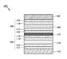
도 1의 (A) 및 (B)는 본 발명의 일 형태에 따른 발광 소자의 단면 모식도.
도 2의 (A) 및 (B)는 본 발명의 일 형태에 따른 발광 소자의 발광층에서의, 에너지 밴드의 상관 및 에너지 준위의 상관을 나타낸 것.
도 3의 (A) 및 (B)는 본 발명의 일 형태에 따른 발광 소자의 단면 모식도.
도 4는 본 발명의 일 형태에 따른 발광 소자의 단면 모식도.
도 5의 (A) 및 (B)는 각각 본 발명의 일 형태에 따른 발광 소자의 단면 모식도.
도 6의 (A) 및 (B)는 각각 본 발명의 일 형태에 따른 발광 소자의 단면 모식도.
도 7의 (A) 내지 (C)는 본 발명의 일 형태에 따른 발광 소자의 제작 방법을 도시한 단면 모식도.
도 8의 (A) 내지 (C)는 본 발명의 일 형태에 따른 발광 소자의 제작 방법을 도시한 단면 모식도.
도 9의 (A) 및 (B)는 본 발명의 일 형태에 따른 표시 장치를 도시한 상면도 및 단면 모식도.
도 10의 (A) 및 (B)는 본 발명의 일 형태에 따른 표시 장치를 각각 도시한 단면 모식도.
도 11은 본 발명의 일 형태에 따른 표시 장치를 도시한 단면 모식도.
도 12의 (A) 및 (B)는 본 발명의 일 형태에 따른 표시 장치를 각각 도시한 단면 모식도.
도 13의 (A) 및 (B)는 본 발명의 일 형태에 따른 표시 장치를 각각 도시한 단면 모식도.
도 14는 본 발명의 일 형태에 따른 표시 장치를 도시한 단면 모식도.
도 15의 (A) 및 (B)는 본 발명의 일 형태에 따른 표시 장치를 각각 도시한 단면 모식도.
도 16은 본 발명의 일 형태에 따른 표시 장치를 도시한 단면 모식도.
도 17의 (A) 및 (B)는 본 발명의 일 형태에 따른 표시 장치를 각각 도시한 단면 모식도.
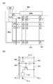
도 18의 (A) 및 (B)는 본 발명의 일 형태에 따른 표시 장치를 도시한 블록도 및 회로도.
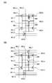
도 19의 (A) 및 (B)는 본 발명의 일 형태에 따른 표시 장치의 화소 회로를 각각 도시한 회로도.
도 20의 (A) 및 (B)는 본 발명의 일 형태에 따른 표시 장치의 화소 회로를 각각 도시한 회로도.
도 21의 (A) 및 (B)는 본 발명의 일 형태에 따른 터치 패널의 예를 도시한 사시도.
도 22의 (A) 내지 (C)는 본 발명의 일 형태에 따른 표시 장치 및 터치 센서의 예를 도시한 단면도.
도 23의 (A) 및 (B)는 본 발명의 일 형태에 따른 터치 패널의 예를 각각 도시한 단면도.
도 24의 (A) 및 (B)는 본 발명의 일 형태에 따른 터치 센서의 블록도 및 타이밍 차트.
도 25는 본 발명의 일 형태에 따른 터치 센서의 회로도.
도 26은 본 발명의 일 형태에 따른 표시 모듈을 도시한 사시도.
도 27의 (A) 내지 (G)는 본 발명의 일 형태에 따른 전자 기기를 도시한 것.
도 28의 (A) 내지 (D)는 본 발명의 일 형태에 따른 전자 기기를 도시한 것.
도 29의 (A) 및 (B)는 본 발명의 일 형태에 따른 표시 장치를 도시한 사시도.
도 30의 (A) 내지 (C)는 본 발명의 일 형태에 따른 발광 장치를 도시한 사시도 및 단면도.
도 31의 (A) 내지 (D)는 본 발명의 일 형태에 따른 발광 장치를 각각 도시한 단면도.
도 32의 (A) 및 (B)는 본 발명의 일 형태에 따른 전자 기기를 도시한 것이고, 도 32의 (C)는 본 발명의 일 형태에 따른 조명 장치를 도시한 것.
도 33은 본 발명의 일 형태에 따른 조명 장치를 도시한 것.
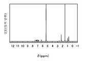
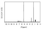
도 34는 본 발명의 일 형태에 따른 화합물의 NMR 차트.
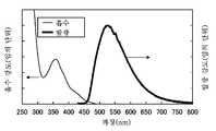
도 35는 본 발명의 일 형태에 따른 화합물의 흡수 스펙트럼 및 발광 스펙트럼을 나타낸 그래프.
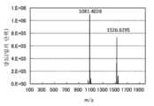
도 36은 본 발명의 일 형태에 따른 화합물의 액체 크로마토그래피 질량 분석을 나타낸 그래프.
도 37은 본 발명의 일 형태에 따른 화합물의 NMR 차트.
도 38은 본 발명의 일 형태에 따른 화합물의 흡수 스펙트럼 및 발광 스펙트럼을 나타낸 그래프.
도 39는 본 발명의 일 형태에 따른 화합물의 NMR 차트.
도 40은 본 발명의 일 형태에 따른 화합물의 흡수 스펙트럼 및 발광 스펙트럼을 나타낸 그래프.
도 41은 본 발명의 일 형태에 따른 화합물의 액체 크로마토그래피 질량 분석을 나타낸 그래프.
도 42는 실시예에서의 발광 소자를 도시한 단면 모식도.
도 43의 (A) 및 (B)는 실시예에서의 호스트 재료의 전계 발광 스펙트럼을 각각 나타낸 그래프.
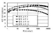
도 44는 실시예에서의 발광 소자의 전류 효율-휘도 특성을 나타낸 그래프.
도 45는 실시예에서의 발광 소자의 휘도-전압 특성을 나타낸 그래프.
도 46은 실시예에서의 발광 소자의 외부 양자 효율-휘도 특성을 나타낸 그래프.
도 47은 실시예에서의 발광 소자의 전력 효율-휘도 특성을 나타낸 그래프.
도 48의 (A) 및 (B)는 실시예에서의 발광 소자의 전계 발광 스펙트럼을 각각 나타낸 그래프.
도 49는 실시예에서의 화합물의 흡수 스펙트럼을 나타낸 것.
도 50은 실시예에서의 발광 소자의 신뢰성 시험 결과를 나타낸 그래프.
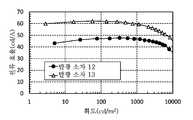
도 51은 실시예에서의 발광 소자의 전류 효율-휘도 특성을 나타낸 그래프.
도 52는 실시예에서의 발광 소자의 휘도-전압 특성을 나타낸 그래프.
도 53은 실시예에서의 발광 소자의 외부 양자 효율-휘도 특성을 나타낸 그래프.
도 54는 실시예에서의 발광 소자의 전력 효율-휘도 특성을 나타낸 그래프.
도 55는 실시예에서의 발광 소자의 전계 발광 스펙트럼을 나타낸 그래프.
도 56은 실시예에서의 발광 소자의 전류 효율-휘도 특성을 나타낸 그래프.
도 57은 실시예에서의 발광 소자의 휘도-전압 특성을 나타낸 그래프.
도 58은 실시예에서의 발광 소자의 전류 밀도-전압 특성을 나타낸 그래프.
도 59는 실시예에서의 발광 소자의 외부 양자 효율-휘도 특성을 나타낸 그래프.
도 60은 실시예에서의 발광 소자의 전력 효율-휘도 특성을 나타낸 그래프.
도 61은 실시예에서의 발광 소자의 전계 발광 스펙트럼을 나타낸 그래프.
도 62는 실시예에서의 발광 소자의 신뢰성 시험 결과를 나타낸 그래프.
도 63은 본 발명의 일 형태에 따른 화합물의 NMR 차트.
도 64는 본 발명의 일 형태에 따른 화합물의 흡수 스펙트럼 및 발광 스펙트럼을 나타낸 그래프.
도 65는 본 발명의 일 형태에 따른 화합물의 액체 크로마토그래피 질량 분석을 나타낸 그래프.
도 66은 본 발명의 일 형태에 따른 화합물의 NMR 차트.
도 67은 본 발명의 일 형태에 따른 화합물의 흡수 스펙트럼 및 발광 스펙트럼을 나타낸 그래프.
도 68은 본 발명의 일 형태에 따른 화합물의 액체 크로마토그래피 질량 분석을 나타낸 그래프.
도 69는 본 발명의 일 형태에 따른 화합물의 NMR 차트.
도 70은 본 발명의 일 형태에 따른 화합물의 흡수 스펙트럼 및 발광 스펙트럼을 나타낸 그래프.
도 71은 본 발명의 일 형태에 따른 화합물의 액체 크로마토그래피 질량 분석을 나타낸 그래프.
도 72는 본 발명의 일 형태에 따른 화합물의 NMR 차트.
도 73은 본 발명의 일 형태에 따른 화합물의 흡수 스펙트럼 및 발광 스펙트럼을 나타낸 그래프.
도 74는 본 발명의 일 형태에 따른 화합물의 액체 크로마토그래피 질량 분석을 나타낸 그래프.
도 75는 본 발명의 일 형태에 따른 화합물의 NMR 차트.
도 76은 본 발명의 일 형태에 따른 화합물의 흡수 스펙트럼 및 발광 스펙트럼을 나타낸 그래프.
도 77은 본 발명의 일 형태에 따른 화합물의 액체 크로마토그래피 질량 분석을 나타낸 그래프.
도 78은 본 발명의 일 형태에 따른 화합물의 NMR 차트.
도 79는 본 발명의 일 형태에 따른 화합물의 흡수 스펙트럼 및 발광 스펙트럼을 나타낸 그래프.
도 80은 본 발명의 일 형태에 따른 화합물의 액체 크로마토그래피 질량 분석을 나타낸 그래프.
도 81은 본 발명의 일 형태에 따른 화합물의 NMR 차트.
도 82는 본 발명의 일 형태에 따른 화합물의 흡수 스펙트럼 및 발광 스펙트럼을 나타낸 그래프.
도 83은 본 발명의 일 형태에 따른 화합물의 NMR 차트.
도 84는 본 발명의 일 형태에 따른 화합물의 흡수 스펙트럼 및 발광 스펙트럼을 나타낸 그래프.
도 85는 실시예에서의 발광 소자의 전류 효율-휘도 특성을 나타낸 그래프.
도 86은 실시예에서의 발광 소자의 휘도-전압 특성을 나타낸 그래프.
도 87은 실시예에서의 발광 소자의 외부 양자 효율-휘도 특성을 나타낸 그래프.
도 88은 실시예에서의 발광 소자의 전력 효율-휘도 특성을 나타낸 그래프.
도 89는 실시예에서의 발광 소자의 전계 발광 스펙트럼을 나타낸 그래프.
도 90은 실시예에서의 호스트 재료의 발광 스펙트럼을 나타낸 그래프.
도 91은 실시예에서의 발광 소자의 전류 효율-휘도 특성을 나타낸 그래프.
도 92는 실시예에서의 발광 소자의 휘도-전압 특성을 나타낸 그래프.
도 93은 실시예에서의 발광 소자의 외부 양자 효율-휘도 특성을 나타낸 그래프.
도 94는 실시예에서의 발광 소자의 전력 효율-휘도 특성을 나타낸 그래프.
도 95는 실시예에서의 발광 소자의 전계 발광 스펙트럼을 나타낸 그래프.
도 96은 실시예에서의 발광 소자의 전류 효율-휘도 특성을 나타낸 그래프.
도 97은 실시예에서의 발광 소자의 휘도-전압 특성을 나타낸 그래프.
도 98은 실시예에서의 발광 소자의 외부 양자 효율-휘도 특성을 나타낸 그래프.
도 99는 실시예에서의 발광 소자의 전력 효율-휘도 특성을 나타낸 그래프.
도 100은 실시예에서의 발광 소자의 전계 발광 스펙트럼을 나타낸 그래프.
도 101은 실시예에서의 발광 소자의 전류 효율-휘도 특성을 나타낸 그래프.
도 102는 실시예에서의 발광 소자의 휘도-전압 특성을 나타낸 그래프.
도 103은 실시예에서의 발광 소자의 외부 양자 효율-휘도 특성을 나타낸 그래프.
도 104는 실시예에서의 발광 소자의 전력 효율-휘도 특성을 나타낸 그래프.
도 105는 실시예에서의 발광 소자의 전계 발광 스펙트럼을 나타낸 그래프.
도 106은 실시예에서의 호스트 재료의 발광 스펙트럼을 나타낸 그래프.
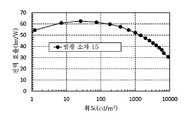
도 107은 실시예에서의 발광 소자의 전류 효율-휘도 특성을 나타낸 그래프.
도 108은 실시예에서의 발광 소자의 휘도-전압 특성을 나타낸 그래프.
도 109는 실시예에서의 발광 소자의 외부 양자 효율-휘도 특성을 나타낸 그래프.
도 110은 실시예에서의 발광 소자의 전력 효율-휘도 특성을 나타낸 그래프.
도 111은 실시예에서의 발광 소자의 전계 발광 스펙트럼을 나타낸 그래프.
도 112는 실시예에서의 화합물의 흡수 스펙트럼을 나타낸 그래프.
도 113은 실시예에서의 발광 소자의 전력 효율-휘도 특성을 나타낸 그래프.
도 114는 실시예에서의 발광 소자의 휘도-전압 특성을 나타낸 그래프.
도 115는 실시예에서의 발광 소자의 외부 양자 효율-휘도 특성을 나타낸 그래프.
도 116은 실시예에서의 발광 소자의 전계 발광 스펙트럼을 나타낸 그래프.
도 117은 실시예에서의 발광 소자로부터의 발광을 나타낸 것.
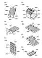
도 118은 본 발명의 일 형태에 따른 화합물의 NMR 차트.
도 119는 본 발명의 일 형태에 따른 화합물의 흡수 스펙트럼 및 발광 스펙트럼을 나타낸 그래프.1 (A) and 1 (B) are cross-sectional schematic views of a light emitting device according to an embodiment of the present invention.
2 (A) and 2 (B) show the correlation of the energy band and the energy level in the light emitting layer of the light emitting device according to an embodiment of the present invention.
3 (A) and 3 (B) are cross-sectional schematic views of a light emitting device according to an embodiment of the present invention.
4 is a cross-sectional schematic diagram of a light emitting device according to an embodiment of the present invention.
5A and 5B are cross-sectional schematic views of a light emitting device according to an embodiment of the present invention, respectively.
6A and 6B are cross-sectional schematic views of a light emitting device according to an embodiment of the present invention, respectively.
7 (A) to 7 (C) are cross-sectional schematic diagrams illustrating a method of manufacturing a light emitting device according to an embodiment of the present invention.
8A to 8C are cross-sectional schematic diagrams illustrating a method of manufacturing a light emitting device according to an embodiment of the present invention.
9 (A) and 9 (B) are a top view and a cross-sectional view showing a display device according to an embodiment of the present invention.
10 (A) and 10 (B) are cross-sectional schematic diagrams each showing a display device according to an embodiment of the present invention.
11 is a cross-sectional schematic diagram showing a display device according to an embodiment of the present invention.
12 (A) and 12 (B) are cross-sectional schematic diagrams each showing a display device according to an embodiment of the present invention.
13 (A) and 13 (B) are cross-sectional views each showing a display device according to an embodiment of the present invention.
14 is a cross-sectional schematic diagram showing a display device according to an embodiment of the present invention.
15 (A) and 15 (B) are cross-sectional schematic diagrams each showing a display device according to an embodiment of the present invention.
16 is a cross-sectional schematic diagram showing a display device according to an embodiment of the present invention.
17 (A) and 17 (B) are cross-sectional schematic diagrams each showing a display device according to an embodiment of the present invention.
18A and 18B are a block diagram and a circuit diagram showing a display device according to an embodiment of the present invention.
19A and 19B are circuit diagrams each showing a pixel circuit of a display device according to an embodiment of the present invention.
20 (A) and 20 (B) are circuit diagrams each showing a pixel circuit of a display device according to an embodiment of the present invention.
21 (A) and 21 (B) are perspective views showing an example of a touch panel according to an embodiment of the present invention.
22 (A) to 22 (C) are cross-sectional views showing examples of a display device and a touch sensor according to an embodiment of the present invention.
23A and 23B are cross-sectional views each showing an example of a touch panel according to an embodiment of the present invention.
24A and 24B are a block diagram and a timing chart of a touch sensor according to an embodiment of the present invention.
25 is a circuit diagram of a touch sensor according to an embodiment of the present invention.
26 is a perspective view showing a display module according to an embodiment of the present invention;
27 (A) to 27 (G) show an electronic apparatus according to an embodiment of the present invention.
28A to 28D show an electronic apparatus according to an embodiment of the present invention.
29A and 29B are perspective views showing a display device according to an embodiment of the present invention.
30 (A) to 30 (C) are a perspective view and a sectional view showing a light emitting device according to an embodiment of the present invention.
31 (A) to 31 (D) are cross-sectional views each showing a light emitting device according to an embodiment of the present invention.
32A and 32B show an electronic apparatus according to an embodiment of the present invention, and FIG. 32C shows a lighting apparatus according to an embodiment of the present invention.
33 shows a lighting apparatus according to an embodiment of the present invention.
34 is an NMR chart of a compound according to an aspect of the present invention.
35 is a graph showing an absorption spectrum and an emission spectrum of a compound according to an embodiment of the present invention.
36 is a graph showing liquid chromatography mass spectrometry of a compound according to an aspect of the present invention.
37 is an NMR chart of a compound according to an aspect of the present invention.
38 is a graph showing an absorption spectrum and an emission spectrum of a compound according to an embodiment of the present invention.
39 is an NMR chart of a compound according to an aspect of the present invention.
40 is a graph showing an absorption spectrum and an emission spectrum of a compound according to an embodiment of the present invention.
41 is a graph showing liquid chromatography mass spectrometry of a compound according to an aspect of the present invention.
42 is a sectional schematic view showing a light emitting element in the embodiment.
43A and 43B are graphs showing the electroluminescence spectra of the host material in the examples, respectively.
44 is a graph showing the current efficiency-luminance characteristic of the light emitting device in the embodiment.
45 is a graph showing the luminance-voltage characteristics of the light emitting device in the embodiment.
46 is a graph showing the external quantum efficiency-luminance characteristic of the light emitting device in the embodiment.
47 is a graph showing power efficiency-luminance characteristics of the light emitting device in the embodiment.
FIGS. 48A and 48B are graphs showing the electroluminescence spectra of the light emitting devices in the examples, respectively. FIG.
49 shows the absorption spectrum of the compound in the examples.
50 is a graph showing a result of reliability test of the light emitting device in the embodiment.
51 is a graph showing the current efficiency-luminance characteristic of the light emitting device in the embodiment.
52 is a graph showing the luminance-voltage characteristics of the light emitting device in the embodiment.
53 is a graph showing the external quantum efficiency-luminance characteristic of the light emitting device in the embodiment.
54 is a graph showing power efficiency-luminance characteristics of the light emitting device in the embodiment.
55 is a graph showing the electroluminescence spectrum of the light emitting device in the embodiment.
56 is a graph showing the current efficiency-luminance characteristics of the light emitting device in the embodiment.
57 is a graph showing the luminance-voltage characteristics of the light emitting device in the embodiment.
58 is a graph showing the current density-voltage characteristics of the light emitting device in the embodiment.
FIG. 59 is a graph showing the external quantum efficiency-luminance characteristic of the light emitting device in the embodiment. FIG.
60 is a graph showing power efficiency-luminance characteristics of the light emitting device in the embodiment.
61 is a graph showing the electroluminescence spectrum of the light emitting device in the embodiment.
62 is a graph showing a result of reliability test of the light emitting device in the embodiment.
63 is an NMR chart of a compound according to an aspect of the present invention.
64 is a graph showing an absorption spectrum and an emission spectrum of a compound according to an embodiment of the present invention;
65 is a graph showing liquid chromatography mass spectrometry of a compound according to an aspect of the present invention.
66 is an NMR chart of a compound according to an aspect of the present invention.
67 is a graph showing an absorption spectrum and an emission spectrum of a compound according to an embodiment of the present invention.
68 is a graph showing liquid chromatography mass spectrometry of a compound according to an aspect of the present invention.
69 is an NMR chart of a compound according to an embodiment of the present invention.
70 is a graph showing an absorption spectrum and an emission spectrum of a compound according to an embodiment of the present invention.
71 is a graph showing liquid chromatography mass spectrometry of a compound according to an aspect of the present invention.
72 is an NMR chart of a compound according to an aspect of the present invention.
73 is a graph showing an absorption spectrum and an emission spectrum of a compound according to an embodiment of the present invention.
74 is a graph showing liquid chromatography mass spectrometry of a compound according to an aspect of the present invention.
75 is an NMR chart of a compound according to an aspect of the present invention.
76 is a graph showing an absorption spectrum and an emission spectrum of a compound according to an embodiment of the present invention.
77 is a graph showing liquid chromatography mass spectrometry of a compound according to an aspect of the present invention.
78 is an NMR chart of a compound according to an aspect of the present invention.
79 is a graph showing an absorption spectrum and an emission spectrum of a compound according to an embodiment of the present invention.
80 is a graph showing liquid chromatography mass spectrometry of a compound according to an aspect of the present invention.
81 is an NMR chart of a compound according to an aspect of the present invention.
82 is a graph showing an absorption spectrum and an emission spectrum of a compound according to an embodiment of the present invention.
83 is an NMR chart of a compound according to an aspect of the present invention.
84 is a graph showing an absorption spectrum and an emission spectrum of a compound according to an embodiment of the present invention.
85 is a graph showing current efficiency-luminance characteristics of the light emitting device in the embodiment.
86 is a graph showing the luminance-voltage characteristic of the light emitting device in the embodiment.
87 is a graph showing the external quantum efficiency-luminance characteristic of the light emitting device in the embodiment.
88 is a graph showing the power efficiency-luminance characteristic of the light emitting device in the embodiment.
89 is a graph showing the electroluminescence spectrum of the light emitting device in the embodiment.
90 is a graph showing the luminescence spectrum of the host material in the examples.
91 is a graph showing current efficiency-luminance characteristics of the light emitting device in the embodiment.
92 is a graph showing the luminance-voltage characteristics of the light emitting element in the embodiment;
93 is a graph showing the external quantum efficiency-luminance characteristic of the light emitting device in the embodiment.
94 is a graph showing power efficiency-luminance characteristics of the light emitting device in the embodiment.
95 is a graph showing the electroluminescence spectrum of the light emitting device in the embodiment.
FIG. 96 is a graph showing the current efficiency-luminance characteristic of the light emitting device in the embodiment. FIG.
97 is a graph showing luminance-voltage characteristics of the light emitting device in the embodiment.
FIG. 98 is a graph showing the external quantum efficiency-luminance characteristic of the light emitting device in the embodiment. FIG.
99 is a graph showing power efficiency-luminance characteristics of the light emitting device in the embodiment.
100 is a graph showing the electroluminescence spectrum of the light emitting device in the embodiment.
101 is a graph showing the current efficiency-luminance characteristic of the light emitting device in the embodiment.
FIG. 102 is a graph showing the luminance-voltage characteristics of the light emitting device in the embodiment. FIG.
103 is a graph showing the external quantum efficiency-luminance characteristic of the light emitting device in the embodiment.
104 is a graph showing power efficiency-luminance characteristics of the light emitting device in the embodiment.
105 is a graph showing an electroluminescence spectrum of the light emitting element in the embodiment.
106 is a graph showing the luminescence spectrum of the host material in the examples.
107 is a graph showing the current efficiency-luminance characteristic of the light emitting device in the embodiment.
108 is a graph showing the luminance-voltage characteristics of the light emitting device in the embodiment.
109 is a graph showing the external quantum efficiency-luminance characteristic of the light emitting device in the embodiment.
110 is a graph showing power efficiency-luminance characteristics of the light emitting device in the embodiment.
FIG. 111 is a graph showing the electroluminescence spectrum of the light emitting device in the embodiment. FIG.
112 is a graph showing absorption spectra of the compounds in Examples.
113 is a graph showing power efficiency-luminance characteristics of the light emitting device in the embodiment.
114 is a graph showing the luminance-voltage characteristics of the light emitting device in the embodiment.
115 is a graph showing the external quantum efficiency-luminance characteristic of the light emitting device in the embodiment.
116 is a graph showing the electroluminescence spectrum of the light emitting device in the embodiment.
117 shows the light emission from the light emitting element in the embodiment.
118 is an NMR chart of a compound according to an aspect of the present invention.
119 is a graph showing an absorption spectrum and an emission spectrum of a compound according to an embodiment of the present invention.
아래에서 본 발명의 실시형태에 대하여 도면을 참조하여 설명한다. 그러나, 본 발명은 아래의 설명에 한정되지 않고, 본 발명의 목적 및 범위로부터 벗어나지 않고 그 형태 및 자세한 사항을 다양하게 변경할 수 있는 것은 용이하게 이해된다. 따라서, 본 발명은 아래의 실시형태의 내용에 한정하여 해석되지 않는다.BEST MODE FOR CARRYING OUT THE INVENTION Hereinafter, embodiments of the present invention will be described with reference to the drawings. However, the present invention is not limited to the following description, and it is easily understood that various changes can be made in form and details without departing from the purpose and scope of the present invention. Therefore, the present invention is not construed as being limited to the contents of the following embodiments.
또한, 도면 등에 도시된 각 구조의 위치, 크기, 또는 범위 등은 간략화를 위하여 정확히 나타내지 않은 경우가 있다. 그러므로, 개시된 발명은 반드시 도면 등에 개시된 위치, 크기, 또는 범위 등에 한정되지는 않는다.In addition, the position, size, or range of each structure shown in the drawings and the like may not be accurately shown for the sake of simplicity. Therefore, the disclosed invention is not necessarily limited to the position, size, or range disclosed in the drawings and the like.
또한, 본 명세서 등에서 "제 1" 및 "제 2" 등의 서수는 편의상 사용하는 것이고, 단계의 순서 또는 적층 순서를 나타내는 것은 아니다. 따라서, 예를 들어, "제 1"을 "제 2" 또는 "제 3"으로 적절히 바꿔도 설명이 가능하다. 또한, 본 명세서 등에서의 서수는 본 발명의 일 형태를 특정하는 것과 반드시 같지는 않다.In the present specification and the like, the ordinal numbers such as " first "and" second "are used for convenience and do not indicate the order of steps or the order of stacking. Therefore, for example, the description can be made by appropriately changing "first" to "second" or "third". In addition, the ordinal numbers in this specification and the like are not necessarily the same as specifying one form of the present invention.
본 명세서 등에서 도면을 참조하여 본 발명의 형태를 설명하는 데 있어, 상이한 도면의 같은 구성 요소는 같은 부호로 공통적으로 표시하는 경우가 있다.In describing the form of the present invention with reference to the drawings in this specification and the like, the same constituent elements in different drawings may be denoted by the same reference numeral in common.
본 명세서 등에서는, 경우 또는 상황에 따라 "막" 및 "층"이라는 용어를 서로 교체할 수 있다. 예를 들어, "도전층"이라는 용어를 "도전막"이라는 용어로 바꿀 수 있는 경우가 있다. 또한, "절연막"이라는 용어를 "절연층"이라는 용어로 바꿀 수 있는 경우가 있다.In this specification and the like, the terms "membrane" and "layer" For example, the term "conductive layer" may be replaced with the term "conductive film ". Further, the term "insulating film" may be replaced with the term "insulating layer ".
본 명세서 등에서, 단일항 여기 상태(S*)는 여기 에너지를 갖는 단일항 상태를 말한다. 단일항 여기 에너지 준위의 가장 낮은 준위(S1 준위)는 가장 낮은 단일항 여기 상태의 여기 에너지 준위를 말한다. 삼중항 여기 상태(T*)는 여기 에너지를 갖는 삼중항 상태를 말한다. 삼중항 여기 에너지 준위의 가장 낮은 준위(T1 준위)는 가장 낮은 삼중항 여기 상태의 여기 에너지 준위를 말한다. 또한, 본 명세서 등에서, 단일항 여기 상태 및 단일항 여기 에너지 준위는 각각 가장 낮은 단일항 여기 상태 및 S1 준위를 의미하는 경우가 있다. 삼중항 여기 상태 및 삼중항 여기 에너지 준위는 각각 가장 낮은 삼중항 여기 상태 및 T1 준위를 의미하는 경우가 있다.In this specification and the like, a singlet anti-excitation state (S* ) refers to a singlet state having excitation energy. The lowest level (S1 level) of the singlet anti-excitation energy level refers to the lowest excitation energy level of singlet anti-excitation state. The triplet excitation state (T* ) refers to a triplet state with excitation energy. The lowest level (T1 level) of the triplet excitation energy level refers to the lowest excited energy level of the triplet excited state. Further, in this specification and the like, the singlet anti-excitation state and the singlet anti-excitation energy level may mean the lowest single excitation state and the S1 state, respectively. The triplet excited state and the triplet excited energy level may each refer to the lowest triplet excited state and the T1 state, respectively.
본 명세서 등에서 형광성 화합물이란, 단일항 여기 상태로부터 기저 상태로 완화될 때에 가시광 영역의 광을 방출하는 화합물을 말한다. 인광성 화합물이란, 삼중항 여기 상태로부터 기저 상태로 완화될 때에 실온에서 가시광 영역의 광을 방출하는 화합물을 말한다. 즉, 인광성 화합물이란, 삼중항 여기 에너지를 가시광으로 변환할 수 있는 화합물을 말한다.In this specification and the like, a fluorescent compound means a compound that emits light in a visible light region when relaxed from a singlet excited state to a ground state. The phosphorescent compound means a compound that emits light in the visible light region at room temperature when relaxed from the triplet excited state to the ground state. That is, the phosphorescent compound refers to a compound capable of converting triplet excitation energy into visible light.
인광 발광 에너지 또는 삼중항 여기 에너지는 인광 발광의 가장 짧은 파장 측의 인광 발광 피크(숄더를 포함함)의 파장으로부터 얻을 수 있다. 또한, 상기 인광 발광은 저온(예를 들어, 10K) 환경에서 시간 분해 광 루미네선스에 의하여 관찰될 수 있다. 열활성화 지연 형광의 발광 에너지란, 열활성화 지연 형광의 가장 짧은 파장 측의 발광 피크(숄더를 포함함)의 파장으로부터 얻을 수 있다.The phosphorescence emission energy or triplet excitation energy can be obtained from the wavelength of the phosphorescence emission peak (including the shoulder) on the shortest wavelength side of phosphorescence emission. In addition, the phosphorescent emission can be observed by time-resolved photoluminescence in a low-temperature (e.g., 10K) environment. The light emission energy of the thermal activation delay fluorescent light can be obtained from the wavelength of the light emission peak (including the shoulder) on the shortest wavelength side of the thermal activation delay fluorescence light.
또한, 본 명세서 등에서 "실온"이란, 0℃ 이상 40℃ 이하의 온도를 말한다.In this specification and the like, "room temperature" refers to a temperature of 0 ° C or higher and 40 ° C or lower.
본 명세서 등에서, 청색의 파장 영역이란 400nm 이상 505nm 미만의 파장 영역을 말하고, 청색광은 발광 스펙트럼의 상기 영역에 적어도 하나의 피크를 갖는다. 녹색의 파장 영역이란 505nm 이상 580nm 미만의 파장 영역을 말하고, 녹색광은 발광 스펙트럼의 상기 영역에 적어도 하나의 피크를 갖는다. 적색의 파장 영역이란 580nm 이상 680nm 이하의 파장 영역을 말하고, 적색광은 발광 스펙트럼의 상기 영역에 적어도 하나의 피크를 갖는다.In the present specification and the like, the blue wavelength region refers to a wavelength region of 400 nm or more and less than 505 nm, and the blue light has at least one peak in the above region of the luminescence spectrum. The green wavelength region refers to a wavelength region of 505 nm or more and less than 580 nm, and the green light has at least one peak in the above region of the emission spectrum. The red wavelength region means a wavelength region of 580 nm or more and 680 nm or less, and the red light has at least one peak in the above region of the emission spectrum.
(실시형태 1)(Embodiment 1)
본 실시형태에서는, 본 발명의 일 형태에 따른 발광 소자에 대하여 도 1의 (A) 및 (B), 및 도 2의 (A) 및 (B)를 참조하여 아래에서 설명한다.In the present embodiment, a light emitting device according to an embodiment of the present invention will be described below with reference to Figs. 1A and 1B, and Figs. 2A and 2B.
<발광 소자의 구조예><Structural Example of Light Emitting Element>
먼저, 본 발명의 일 형태에 따른 발광 소자의 구조에 대하여 도 1의 (A) 및 (B)를 참조하여 설명한다.First, the structure of a light emitting device according to an embodiment of the present invention will be described with reference to Figs. 1A and 1B.
도 1의 (A)는 본 발명의 일 형태에 따른 발광 소자(150)의 단면 모식도이다.1 (A) is a schematic cross-sectional view of a
발광 소자(150)는 한 쌍의 전극(전극(101) 및 전극(102)), 및 한 쌍의 전극 사이의 EL층(100)을 포함한다. EL층(100)은 적어도 발광층(130)을 포함한다.The
도 1의 (A)에 도시된 EL층(100)은 발광층(130)에 더하여, 정공 주입층(111), 정공 수송층(112), 전자 수송층(118), 및 전자 주입층(119) 등의 기능층을 포함한다.The
본 실시형태에서는, 한 쌍의 전극에서 전극(101) 및 전극(102)이 각각 양극 및 음극으로서 기능하는 것으로 상정하여 설명하지만, 발광 소자(150)의 구조는 이에 한정되지 않는다. 즉, 전극(101)이 음극이어도 좋고, 전극(102)이 양극이어도 좋고, 전극들 사이의 층들의 적층 순서가 거꾸로 되어도 좋다. 바꿔 말하면, 정공 주입층(111), 정공 수송층(112), 발광층(130), 전자 수송층(118), 및 전자 주입층(119)이 양극 측으로부터 이 순서대로 적층될 수 있다.In the present embodiment, it is assumed that the
EL층(100)의 구조는 도 1의 (A)에 도시된 구조에 한정되지 않고, 정공 주입층(111), 정공 수송층(112), 전자 수송층(118), 및 전자 주입층(119)에서 선택된 적어도 하나의 층을 포함하는 구조를 채용할 수 있다. 또는, EL층(100)은 예를 들어, 정공 또는 전자의 주입 장벽을 저감하거나, 정공 또는 전자 수송성을 향상시키거나, 정공 또는 전자 수송성을 저해하거나, 또는 전극에 의한 퀀칭 현상을 억제할 수 있는 기능층을 포함하여도 좋다. 또한, 기능층 각각은 단층이어도 좋고 적층이어도 좋다.The structure of the
도 1의 (B)는 도 1의 (A)의 발광층(130)의 예를 도시한 단면 모식도이다. 도 1의 (B)의 발광층(130)은 호스트 재료(131) 및 게스트 재료(132)를 포함한다. 호스트 재료(131)는 유기 화합물(131_1) 및 유기 화합물(131_2)을 포함한다.FIG. 1B is a schematic cross-sectional view showing an example of the
게스트 재료(132)는 발광성 유기 화합물이어도 좋고, 이 발광성 유기 화합물은 인광을 방출할 수 있는 물질(이후, 인광성 화합물이라고도 함)인 것이 바람직하다. 인광성 화합물을 게스트 재료(132)로서 사용하는 구조에 대하여 아래에서 설명한다. 게스트 재료(132)를 인광성 화합물로 바꿔 말하여도 좋다.The
<발광 소자의 발광 기구>≪ Light emitting mechanism of light emitting element &
다음으로, 발광층(130)의 발광 기구에 대하여 아래에서 설명한다.Next, the light emitting mechanism of the
발광층(130)에서의 호스트 재료(131)에 포함되는 유기 화합물(131_1) 및 유기 화합물(131_2)은 엑시플렉스를 형성한다.The organic compound 131_1 and the organic compound 131_2 contained in the
유기 화합물(131_1)과 유기 화합물(131_2)의 조합이 엑시플렉스를 형성할 수 있기만 하면 좋지만, 이들 중 한쪽이 정공을 수송하는 기능(정공 수송성)을 갖는 화합물이고, 다른 쪽이 전자를 수송하는 기능(전자 수송성)을 갖는 화합물인 것이 바람직하다. 이러한 경우에는, 도너-억셉터 엑시플렉스를 형성하기 쉽기 때문에, 엑시플렉스를 효율적으로 형성할 수 있다.It is sufficient if the combination of the organic compound 131_1 and the organic compound 131_2 is capable of forming an exciplex. One of them is a compound having a function of transporting holes (hole transporting property) and the other is a compound having a function of transporting electrons (Electron transporting property). In such a case, since the donor-acceptor exciplex is easily formed, the exciplex can be efficiently formed.
유기 화합물(131_1)과 유기 화합물(131_2)의 조합은, 한쪽이 다른 쪽보다 낮은 HOMO(highest occupied molecular orbital) 준위와 낮은 LUMO(lowest unoccupied molecular orbital) 준위를 갖는 것이 바람직하다.It is preferable that the combination of the organic compound 131_1 and the organic compound 131_2 has a highest occupied molecular orbital (HOMO) level and a lowest unoccupied molecular orbital (LUMO) level.
예를 들어, 도 2의 (A)의 에너지 밴드도에 나타낸 바와 같이, 유기 화합물(131_1)이 전자 수송성을 갖고 유기 화합물(131_2)이 정공 수송성을 갖는 경우, 유기 화합물(131_1)의 HOMO 준위는 유기 화합물(131_2)의 HOMO 준위보다 낮고, 유기 화합물(131_1)의 LUMO 준위는 유기 화합물(131_2)의 LUMO 준위보다 낮은 것이 바람직하다.For example, as shown in the energy band diagram of FIG. 2A, when the organic compound 131_1 has the electron transporting property and the organic compound 131_2 has the hole transporting property, the HOMO level of the organic compound 131_1 is Is lower than the HOMO level of the organic compound (131_2), and the LUMO level of the organic compound (131_1) is lower than the LUMO level of the organic compound (131_2).
이때, 유기 화합물(131_1) 및 유기 화합물(131_2)에 의하여 형성되는 엑시플렉스는, 유기 화합물(131_1)의 LUMO 준위와 유기 화합물(131_2)의 HOMO 준위의 에너지 차이에 실질적으로 상당하는 여기 에너지를 갖는다. 유기 화합물(131_1)의 HOMO 준위와 유기 화합물(131_2)의 HOMO 준위의 차이는 바람직하게는 0.1eV 이상이고, 더 바람직하게는 0.2eV 이상이다. 마찬가지로, 유기 화합물(131_1)의 LUMO 준위와 유기 화합물(131_2)의 LUMO 준위의 차이는 바람직하게는 0.1eV 이상이고, 더 바람직하게는 0.2eV 이상이다. 이 에너지 차이는 한 쌍의 전극(전극(101) 및 전극(102))으로부터 유기 화합물(131_1) 및 유기 화합물(131_2)로의 전자 캐리어 및 정공 캐리어의 주입을 용이하게 하기 때문에 바람직하다. 또한, 도 2의 (A)에서 Host(131_1)는 유기 화합물(131_1)을 나타내고, Host(131_2)는 유기 화합물(131_2)을 나타내고, Guest(132)는 게스트 재료(132)를 나타내고, ΔEEx는 유기 화합물(131_1)의 LUMO 준위와 유기 화합물(131_2)의 HOMO 준위의 에너지 차이를 나타내고, ΔEG는 게스트 재료(132)의 LUMO 준위와 HOMO 준위의 에너지 차이를 나타낸다.At this time, the exciplex formed by the organic compound 131_1 and the organic compound 131_2 has excitation energy substantially corresponding to the energy difference between the LUMO level of the organic compound 131_1 and the HOMO level of the organic compound 131_2 . The difference between the HOMO level of the organic compound 131_1 and the HOMO level of the organic compound 131_2 is preferably 0.1 eV or more, more preferably 0.2 eV or more. Likewise, the difference between the LUMO level of the organic compound 131_1 and the LUMO level of the organic compound 131_2 is preferably 0.1 eV or more, and more preferably 0.2 eV or more. This energy difference is preferable because it facilitates the injection of an electron carrier and a hole carrier from the pair of electrodes (the
게스트 재료(132)의 HOMO 준위는 유기 화합물(131_2)의 HOMO 준위보다 낮고, 게스트 재료(132)의 LUMO 준위는 유기 화합물(131_1)의 LUMO 준위보다 높은 것이 바람직하다. 즉, 게스트 재료(132)의 LUMO 준위와 HOMO 준위의 에너지 차이(ΔEG)는 유기 화합물(131_1)의 LUMO 준위와 유기 화합물(131_2)의 HOMO 준위의 에너지 차이(ΔEEx)보다 크다. 따라서, 게스트 재료(132) 및 유기 화합물(131_1) 또는 유기 화합물(131_2)에 의한 엑시플렉스의 형성을 억제할 수 있다.It is preferable that the HOMO level of the
예를 들어, 게스트 재료(132)의 HOMO 준위가 유기 화합물(131_2)의 HOMO 준위 이상이고, 발광층(130)에 포함되는 재료 중 가장 높은 HOMO 준위를 게스트 재료(132)가 갖고, 가장 낮은 LUMO 준위를 유기 화합물(131_1)이 갖는 경우, 게스트 재료(132) 및 유기 화합물(131_1)이 엑시플렉스를 형성할 가능성이 있다. 특히, 게스트 재료(132)의 HOMO 준위와 유기 화합물(131_1)의 LUMO 준위의 에너지 차이가 게스트 재료의 발광 에너지보다 작아질수록, 게스트 재료(132) 및 유기 화합물(131_1)에 의하여 엑시플렉스가 형성되기 쉬워진다. 이러한 경우, 게스트 재료(132) 자체는 여기 상태를 형성하기 어렵기 때문에, 발광 소자의 발광 효율이 저하된다.For example, the HOMO level of the
예를 들어, 게스트 재료(132)의 LUMO 준위가 유기 화합물(131_1)의 LUMO 준위 이하이고, 발광층(130)에 포함되는 재료 중 가장 낮은 LUMO 준위를 게스트 재료(132)가 갖고, 가장 높은 HOMO 준위를 유기 화합물(131_2)이 갖는 경우, 게스트 재료(132) 및 유기 화합물(131_2)이 엑시플렉스를 형성할 가능성이 있다. 특히, 게스트 재료(132)의 LUMO 준위와 유기 화합물(131_2)의 HOMO 준위의 에너지 차이가 게스트 재료의 발광 에너지보다 작아질수록, 게스트 재료(132) 및 유기 화합물(131_2)에 의하여 엑시플렉스가 형성되기 쉬워진다. 이러한 경우, 게스트 재료(132) 자체는 여기 상태를 형성하기 어렵기 때문에, 발광 소자의 발광 효율이 저하된다.For example, the
그러나, 본 발명의 일 형태에 따른 발광 소자에서는, 게스트 재료(132) 및 유기 화합물(131_1) 또는 유기 화합물(131_2)에 의한 엑시플렉스의 형성을 억제할 수 있기 때문에, 발광 효율이 높은 발광 소자를 제작할 수 있다.However, in the light emitting device according to an embodiment of the present invention, formation of exciplex by the
게스트 재료(132)의 HOMO 준위는 유기 화합물(131_2)의 HOMO 준위보다 낮고, 게스트 재료(132)의 LUMO 준위는 유기 화합물(131_1)의 LUMO 준위보다 높다. 한 쌍의 전극(전극(101) 및 전극(102))으로부터 주입된 캐리어(정공 및 전자) 중, 양극으로부터 주입된 정공은 발광층(130)에서 유기 화합물(131_2)에 주입되기 쉽고, 음극으로부터 주입된 전자는 발광층(130)에서 유기 화합물(131_1)에 주입되기 쉽다.The HOMO level of the
상술한 관점에서, 본 발명의 일 형태에서는, 게스트 재료(132)의 HOMO 준위가 유기 화합물(131_2)의 HOMO 준위와 동등하여도 좋고, 게스트 재료(132)의 LUMO 준위가 유기 화합물(131_1)의 LUMO 준위와 동등하여도 좋다. 그러나, 게스트 재료(132)의 LUMO 준위와 HOMO 준위의 에너지 차이(ΔEG)는 유기 화합물(131_1)의 LUMO 준위와 유기 화합물(131_2)의 HOMO 준위의 에너지 차이(ΔEEx)보다 큰 것이 바람직하다. 이 이유를 아래에서 설명한다.The HOMO level of the
유기 화합물(131_1)의 LUMO 준위와 유기 화합물(131_2)의 HOMO 준위의 에너지 차이(ΔEEx)는 유기 화합물(131_1)의 LUMO 준위와 HOMO 준위의 에너지 차이보다 작고, 유기 화합물(131_2)의 LUMO 준위와 HOMO 준위의 에너지 차이보다 작기 때문에, 유기 화합물(131_1) 및 유기 화합물(131_2)에 의한 엑시플렉스의 형성은 유기 화합물(131_1) 및 유기 화합물(131_2) 중 어느 한쪽만에 의한 여기 상태의 형성보다 더 에너지적으로 안정된다. 또한, 게스트 재료(132)의 LUMO 준위와 HOMO 준위의 에너지 차이(ΔEG)는 유기 화합물(131_1)의 LUMO 준위와 유기 화합물(131_2)의 HOMO 준위의 에너지 차이(ΔEEx)보다 크기 때문에, 발광층(130)에 주입된 캐리어(정공 및 전자)의 재결합에 의하여 형성되는 여기 상태로서는, 유기 화합물(131_1) 및 유기 화합물(131_2)에 의한 엑시플렉스의 형성이 에너지적으로 더 안정된다. 따라서, 발광층(130)에서 생성되는 대부분의 여기 상태는 유기 화합물(131_1) 및 유기 화합물(131_2)에 의하여 형성되는 엑시플렉스로서 존재한다.The energy difference (ΔEEx ) between the LUMO level of the organic compound 131_1 and the HOMO level of the organic compound 131_2 is smaller than the energy difference between the LUMO level and the HOMO level of the organic compound 131_1 and the LUMO level of the organic compound 131_2 The formation of exciplex by the organic compound 131_1 and the organic compound 131_2 is less than the formation of the excited state by either the organic compound 131_1 or the organic compound 131_2 It is more energetically stable. Further, since the energy difference between the LUMO level and the HOMO level of the guest material (132) (ΔEG) is larger than the energy difference between the HOMO energy (ΔEEx) of the LUMO level and the organic compound (131_2) of the organic compound (131_1), a light-emitting layer The formation of exciplex by the organic compound 131_1 and the organic compound 131_2 is energetically more stable as an excited state formed by recombination of the carriers (holes and electrons) injected into the
게스트 재료(132)는 인광성 발광 재료이기 때문에, 삼중항 여기 에너지를 발광으로 변환시키는 기능을 갖는다. 또한, 단일항 여기 상태에서보다 삼중항 여기 상태에서 에너지는 더 안정된다. 따라서, 게스트 재료(132)는 게스트 재료(132)의 LUMO 준위와 HOMO 준위의 에너지 차이(ΔEG)보다 에너지가 작은 광을 방출할 수 있다. 게스트 재료(132)의 LUMO 준위와 HOMO 준위의 에너지 차이(ΔEG)가 유기 화합물(131_1)의 LUMO 준위와 유기 화합물(131_2)의 HOMO 준위의 에너지 차이(ΔEEx)보다 큰 경우에도, 게스트 재료(132)의 발광 에너지 또는 흡수 스펙트럼으로부터 얻어지는 전이 에너지가 ΔEEx 이하이기만 하면, 유기 화합물(131_1) 및 유기 화합물(131_2)에 의하여 형성되는 엑시플렉스로부터 게스트 재료(132)로의 여기 에너지의 이동이 가능하고, 게스트 재료(132)로부터 발광을 얻을 수 있다는 것을 본 발명의 발명자들은 알아내었다. 게스트 재료(132)의 ΔEG가 게스트 재료(132)의 발광 에너지 또는 흡수 스펙트럼으로부터 얻어지는 전이 에너지보다 큰 경우, 게스트 재료(132)의 전기 여기를 직접 일으키기 위해서는 ΔEG에 상당하는 높은 전기 에너지가 필요하므로, 구동 전압이 상승된다. 그러나, 본 발명의 일 형태에서는, ΔEEx(ΔEG보다 작음)에 대응하는 전기 에너지에 의하여 엑시플렉스가 전기적으로 여기되고, 거기에서의 에너지 이동에 의하여 게스트 재료(132)로부터의 발광을 얻을 수 있기 때문에, 효율이 높은 게스트 재료의 발광을 낮은 전압으로 얻을 수 있다. 즉, 본 발명의 일 형태는, ΔEG가 게스트 재료(132)의 발광 에너지 또는 흡수 스펙트럼으로부터 얻어지는 전이 에너지보다 상당히 큰 경우(예를 들어, 게스트 재료가 청색 발광 재료인 경우)에 유용하다.Since the
또한, 게스트 재료(132)가 중금속을 포함하는 경우, 스핀 궤도 상호 작용(전자의 스핀각의 운동량과 궤도각 운동량의 상호 작용)에 의하여 단일항 상태와 삼중항 상태의 항간 교차가 촉진되기 때문에, 게스트 재료(132)의 단일항 기저 상태와 삼중항 여기 상태 사이의 전이가 금지되지 않는 경우가 있다. 그러므로, 게스트 재료(132)의 단일항 기저 상태와 삼중항 여기 상태 사이의 전이에 관한 발광 효율 및 흡수 확률을 높일 수 있다. 따라서, 게스트 재료(132)는 스핀 궤도 상호 작용이 큰 금속 원소, 특히 백금족 원소(루테늄(Ru), 로듐(Rh), 팔라듐(Pd), 오스뮴(Os), 이리듐(Ir), 또는 백금(Pt))를 포함하는 것이 바람직하다. 특히, 이리듐은, 단일항 기저 상태와 삼중항 여기 상태 사이의 직접 전이에 관한 흡수 확률을 높일 수 있기 때문에 바람직하다.In addition, when the
상술한 바와 같이, 게스트 재료(132)의 LUMO 준위와 HOMO 준위의 에너지 차이(ΔEG)가 유기 화합물(131_1)의 LUMO 준위와 유기 화합물(131_2)의 HOMO 준위의 에너지 차이(ΔEEx)보다 크더라도, 게스트 재료(132)의 흡수단으로부터 얻어지는 전이 에너지(약칭: ΔEG_abs)가 ΔEEx 이하이기만 하면, 유기 화합물(131_1) 및 유기 화합물(131_2)에 의하여 형성되는 엑시플렉스로부터 게스트 재료(132)로 여기 에너지가 효율적으로 이동된다. 그 결과, 발광 효율이 높고 구동 전압이 낮은 발광 소자를 얻을 수 있고, 이는 본 발명의 일 형태의 특징이다. 이때, ΔEG_abs≤ΔEEx<ΔEG(ΔEG_abs는 ΔEEx 이하이고, ΔEEx는 ΔEG보다 작음)의 식이 만족된다. 따라서, 게스트 재료(132)의 흡수단으로부터 얻어지는 전이 에너지(ΔEG_abs)가 게스트 재료(132)의 LUMO 준위와 HOMO 준위의 에너지 차이(ΔEG)보다 작은 경우에 본 발명의 일 형태의 메커니즘은 적합하다. 바꿔 말하면, 게스트 재료(132)의 LUMO 준위와 HOMO 준위의 에너지 차이(ΔEG)가 게스트 재료(132)의 흡수단으로부터 얻어지는 전이 에너지(ΔEG_abs)보다 큰 경우에 본 발명의 일 형태의 메커니즘은 적합하다. 구체적으로는, 게스트 재료(132)의 LUMO 준위와 HOMO 준위의 에너지 차이(ΔEG)는 게스트 재료(132)의 흡수단으로부터 얻어지는 전이 에너지(ΔEG_abs)보다 0.4eV 이상 큰 것이 바람직하다. 게스트 재료(132)의 발광 에너지는 ΔEG_abs 이하이기 때문에, 게스트 재료(132)의 LUMO 준위와 HOMO 준위의 에너지 차이(ΔEG)는 게스트 재료(132)의 발광 에너지보다 0.4eV 이상 큰 것이 바람직하다. 또한, 발광 에너지는 발광 스펙트럼의 가장 짧은 파장 측의 피크 파장(극댓값, 또는 숄더 피크를 포함함)으로부터 도출할 수 있다.As described above, the energy difference (? EG ) between the LUMO level and the HOMO level of the
게스트 재료(132)의 발광 파장이 짧아질수록(발광 에너지가 높아질수록), 게스트 재료(132)의 LUMO 준위와 HOMO 준위의 에너지 차이(ΔEG)는 커지므로, 게스트 재료를 전기적으로 여기시키기 위해서는 더 큰 에너지가 필요하다. 그러나, 게스트 재료(132)의 흡수단으로부터 얻어지는 전이 에너지(ΔEG_abs)가 ΔEEx 이하이면, 본 발명에 따라, ΔEG보다 매우 작은 ΔEEx정도의 에너지로 게스트 재료(132)를 여기시킬 수 있기 때문에, 발광 소자의 소비전력을 저감할 수 있다. 따라서, 게스트 재료(132)의 흡수단으로부터 얻어지는 전이 에너지(ΔEG_abs)와, 게스트 재료(132)의 LUMO 준위와 HOMO 준위의 에너지 차이(ΔEG)의 에너지 차이가 큰 경우(즉, 특히 게스트 재료가 청색 발광 재료인 경우)에 본 발명의 일 형태의 메커니즘의 효과가 표면화된다.The emission wavelength of the
게스트 재료(132)의 흡수단으로부터 얻어지는 전이 에너지(ΔEG_abs)가 저하되면, 게스트 재료(132)의 발광 에너지도 저하된다. 이러한 경우에는, 청색 발광 등 높은 에너지를 필요로 하는 발광을 얻기 어렵다. 즉, ΔEG_abs와 ΔEG의 차이가 지나치게 크면, 청색 발광 등 에너지가 높은 발광을 얻기 어렵다.When the transition energy (DELTAEG_abs ) obtained from the absorption edge of the
이러한 이유로, 게스트 재료(132)의 LUMO 준위와 HOMO 준위의 에너지 차이(ΔEG)는 게스트 재료(132)의 흡수단으로부터 얻어지는 전이 에너지(ΔEG_abs)보다 0.4eV 내지 0.8eV만큼 큰 것이 바람직하고, 0.5eV 내지 0.8eV만큼 큰 것이 더 바람직하다. 게스트 재료(132)의 발광 에너지는 ΔEG_abs 이하이기 때문에, 게스트 재료(132)의 LUMO 준위와 HOMO 준위의 에너지 차이(ΔEG)는 게스트 재료(132)의 발광 에너지보다 0.4eV 내지 0.8eV만큼 큰 것이 바람직하고, 0.5eV 내지 0.8eV만큼 큰 것이 더 바람직하다.For this reason, the energy difference between the LUMO level and the HOMO level of the guest material 132 (ΔEG) is to be large enough to 0.4eV to about 0.8eV than the transition energy (ΔEG_abs) obtained from the absorption edge of the
게스트 재료(132)와 유기 화합물(131_1)의 LUMO 준위의 차이는 바람직하게는 0.05eV 이상, 더 바람직하게는 0.1eV 이상, 더욱 바람직하게는 0.2eV 이상이다. 게스트 재료(132)와 유기 화합물(131_2)의 HOMO 준위의 차이는 바람직하게는 0.05eV 이상, 더 바람직하게는 0.1eV 이상, 더욱 바람직하게는 0.2eV 이상이다. 상술한 범위 내로 상기 차이를 설정하면, 유기 화합물(131_1) 및 유기 화합물(131_2)로의 전자 캐리어 및 정공 캐리어의 주입이 용이해지기 때문에 바람직하다.The difference between the LUMO levels of the
또한, 게스트 재료(132)의 HOMO 준위는 유기 화합물(131_1)의 HOMO 준위보다 높아도 좋고 낮아도 좋다. 마찬가지로, 게스트 재료(132)의 LUMO 준위는 유기 화합물(131_2)의 LUMO 준위보다 높아도 좋고 낮아도 좋다.The HOMO level of the
상술한 LUMO 준위와 HOMO 준위의 관계에 따르면, 유기 화합물(131_1)과 유기 화합물(131_2)의 조합을, 한쪽의 산화 전위 및 환원 전위가 다른 쪽보다 높아지도록 하는 것이 바람직하다.According to the above-described relationship between the LUMO level and the HOMO level, it is preferable that the combination of the organic compound 131_1 and the organic compound 131_2 is made such that the oxidation potential and the reduction potential on one side are higher than those on the other side.
예를 들어, 유기 화합물(131_1)이 전자 수송성을 갖고, 유기 화합물(131_2)이 정공 수송성을 갖는 경우, 유기 화합물(131_1)의 산화 전위가 유기 화합물(131_2)의 산화 전위보다 높고, 유기 화합물(131_1)의 환원 전위가 유기 화합물(131_2)의 환원 전위보다 높은 것이 바람직하다. 또한, 산화 전위 및 환원 전위는 사이클릭 볼타메트리(CV)에 의하여 측정할 수 있다.For example, when the organic compound 131_1 has the electron transporting property and the organic compound 131_2 has the hole transporting property, the oxidation potential of the organic compound 131_1 is higher than the oxidation potential of the organic compound 131_2, 131_1) is higher than the reduction potential of the organic compound (131_2). The oxidation potential and the reduction potential can be measured by cyclic voltammetry (CV).
게스트 재료(132)의 산화 전위는 유기 화합물(131_2)의 산화 전위보다 높고, 게스트 재료(132)의 환원 전위는 유기 화합물(131_1)의 환원 전위보다 낮은 것이 바람직하다. 따라서, 상술한 바와 같이, 게스트 재료(132) 및 유기 화합물(131_1) 또는 유기 화합물(131_2)에 의한 엑시플렉스의 형성을 억제할 수 있다.It is preferable that the oxidation potential of the
유기 화합물(131_1)과 유기 화합물(131_2)의 조합이 정공 수송성을 갖는 화합물과 전자 수송성을 갖는 화합물의 조합인 경우, 그 혼합비에 따라 캐리어 밸런스를 쉽게 제어할 수 있다. 구체적으로는, 정공 수송성을 갖는 화합물 대 전자 수송성을 갖는 화합물의 중량비가 1:9 내지 9:1의 범위 내에 있는 것이 바람직하다. 이 구조로 함으로써 캐리어 밸런스를 쉽게 제어할 수 있어, 캐리어 재결합 영역도 쉽게 제어할 수 있다.When the combination of the organic compound 131_1 and the organic compound 131_2 is a combination of a compound having a hole-transporting property and a compound having an electron-transporting property, the carrier balance can be easily controlled according to the mixing ratio. Specifically, it is preferable that the weight ratio of the compound having hole-transporting property to the compound having electron-transporting property is in the range of 1: 9 to 9: 1. With this structure, the carrier balance can be easily controlled, and the carrier recombination region can be easily controlled.
유기 화합물(131_1) 및 유기 화합물(131_2)에 의하여 형성되는 엑시플렉스는 한쪽의 유기 화합물에 HOMO를 갖고, 다른 쪽의 유기 화합물에 LUMO를 갖기 때문에, HOMO와 LUMO의 중첩이 매우 작다. 즉, 상기 엑시플렉스는 단일항 여기 에너지 준위와 삼중항 여기 에너지 준위의 차이가 작다. 따라서, 유기 화합물(131_1) 및 유기 화합물(131_2)에 의하여 형성되는 엑시플렉스의 삼중항 여기 에너지 준위와 단일항 여기 에너지 준위의 차이는 바람직하게는 0eV보다 크고 0.2eV 이하이다.Since the exciplex formed by the organic compound 131_1 and the organic compound 131_2 has HOMO in one organic compound and LUMO in the other organic compound, superposition of HOMO and LUMO is very small. That is, the exciplex has a small difference between the singlet excitation energy level and the triplet excitation energy level. Therefore, the difference between the triplet excitation energy level of the exciplex formed by the organic compound 131_1 and the organic compound 131_2 and the single excitation energy level is preferably greater than 0 eV and less than 0.2 eV.
도 2의 (B)는 발광층(130)에서의 유기 화합물(131_1), 유기 화합물(131_2), 및 게스트 재료(132)의 에너지 준위의 상관을 나타낸 것이다. 도 2의 (B)에서의 용어 및 부호가 나타내는 것에 대하여 아래에서 설명한다.2B shows a correlation between the energy levels of the organic compound 131_1, the organic compound 131_2, and the
Host(131_1): 호스트 재료(유기 화합물(131_1));Host 131_1: host material (organic compound 131_1);
Host(131_2): 호스트 재료(유기 화합물(131_2));Host 131_2: host material (organic compound 131_2);
Guest(132): 게스트 재료(132)(인광성 화합물);Guest 132: guest material 132 (phosphorescent compound);
SPH: 호스트 재료의 S1 준위(유기 화합물(131_1));SPH : S1 level of the host material (organic compound 131_1);
TPH: 호스트 재료의 T1 준위(유기 화합물(131_1));TPH : T1 level of the host material (organic compound 131_1);
SPG: 인광성 화합물의 S1 준위(게스트 재료(132));SPG : S1 level of the phosphorescent compound (guest material 132);
TPG: 인광성 화합물의 T1 준위(게스트 재료(132));TPG : T1 level of the phosphorescent compound (guest material 132);
SPE: 엑시플렉스의 S1 준위; 및SPE : S1 level of exciplex; And
TPE: 엑시플렉스의 T1 준위.TPE : T1 level of exciplex.
본 발명의 일 형태에 따른 발광 소자에서는, 발광층(130)에 포함되는 유기 화합물(131_1 및 131_2)이 엑시플렉스를 형성한다. 엑시플렉스(SPE)의 가장 낮은 단일항 여기 에너지 준위와 엑시플렉스(TPE)의 가장 낮은 삼중항 여기 에너지 준위는 서로 인접된다(도 2의 (B)의 경로 E7 참조).In the light emitting device according to an embodiment of the present invention, the organic compounds 131_1 and 131_2 included in the
엑시플렉스는 2종류의 물질로 형성되는 여기 상태이다. 광 여기에서는, 여기 상태에 있는 한쪽의 물질과 기저 상태에 있는 다른 쪽의 물질의 상호 작용에 의하여 엑시플렉스가 형성된다. 엑시플렉스를 형성한 2종류의 물질은 광을 방출함으로써 기저 상태로 되돌아가고, 원래의 2종류의 물질로서 작용한다. 전기 여기에서는, 한쪽의 물질이 여기 상태가 되면, 이 물질은 바로 다른 쪽의 물질과 상호 작용하여 엑시플렉스를 형성한다. 또는, 한쪽의 물질이 정공을 받고 다른 쪽의 물질이 전자를 받으면 즉시 엑시플렉스가 형성된다. 이러한 경우, 어느 물질에 의해서도 단체로 여기 상태를 형성할 일 없이 엑시플렉스를 형성할 수 있기 때문에, 발광층(130)에서 생성되는 여기 상태의 대부분이 엑시플렉스로서 존재할 수 있다. 엑시플렉스의 여기 에너지 준위(SE 또는 TE)는 엑시플렉스를 형성하는 호스트 재료(유기 화합물(131_1) 및 유기 화합물(131_2))의 단일항 여기 에너지 준위(SPH)보다 낮기 때문에, 더 낮은 여기 에너지로 호스트 재료(131)의 여기 상태를 형성할 수 있다. 이로써, 발광 소자(150)의 구동 전압을 저감할 수 있다.Exciplex is an excited state formed of two kinds of materials. In optics, an exciplex is formed by the interaction of one substance in the excited state and the other substance in the ground state. The two kinds of materials forming the exciplex return to the ground state by emitting light and act as original two kinds of materials. Electrically, when one material is in an excited state, it interacts with the other directly to form an exciplex. Alternatively, when one material receives holes and the other material receives electrons, an exciplex is formed immediately. In this case, since exciplex can be formed without forming any excited state by any substance, most of the excited state generated in the
그리고, 엑시플렉스의 SPE 및 TPE의 에너지 양쪽을 게스트 재료(132)(인광성 화합물)의 가장 낮은 삼중항 여기 상태의 준위(TPG)로 이동시키면, 발광이 얻어진다(도 2의 (B)의 경로 E8 및 E9 참조).Then, when both the energy of SPE and TPE of the exciplex are moved to the lowest triplet excited state level (TPG ) of the guest material 132 (phosphorescent compound), light emission is obtained B path) reference E8 and E9).
또한, 엑시플렉스의 삼중항 여기 에너지 준위(TPE)는 게스트 재료(132)의 삼중항 여기 에너지 준위(TPG)보다 높은 것이 바람직하다. 이렇게 하면, 형성된 엑시플렉스의 단일항 여기 에너지 및 삼중항 여기 에너지를, 엑시플렉스의 단일항 여기 에너지 준위(SPE) 및 삼중항 여기 에너지 준위(TPE)로부터 게스트 재료(132)의 삼중항 여기 에너지 준위(TPG)로 이동시킬 수 있다.It is also preferable that the triplet excitation energy level (TPE ) of the exciplex is higher than the triplet excitation energy level (TPG ) of the
발광층(130)이 상술한 구조를 가지면, 발광층(130)의 게스트 재료(132)(인광성 화합물)로부터의 발광을 효율적으로 얻을 수 있다.When the
경로 E7, E8, 및 E9를 거친 상술한 과정을 본 명세서 등에서 ExTET(exciplex-triplet energy transfer)라고 할 수 있다. 바꿔 말하면, 발광층(130)에서는, 엑시플렉스로부터 게스트 재료(132)로 여기 에너지가 주어진다. 이러한 경우, TPE로부터 SPE로의 역항간 교차 효율은 반드시 높을 필요는 없고, SPE로부터의 발광 양자 수율도 반드시 높을 필요는 없기 때문에, 재료를 폭넓은 선택지 중에서 선택할 수 있다.The above-described process passed through the path E7, E8, E9, and can be said ExTET (exciplex-triplet energy transfer), etc. The present disclosure. In other words, in the
또한, 상술한 반응은 일반식(G11) 내지 일반식(G13)으로 나타낼 수 있다.Further, the above-mentioned reaction can be represented by the general formulas (G11) to (G13).
D++A- (D·A)*(G11)D+ + A- (D * A)* (G11)
(D·A)*+G D+A+G*(G12)(D · A)* + G D + A + G* (G12)
G* G+hν(G13)G* G + hv (G13)
일반식(G11)에서는, 유기 화합물(131_1) 및 유기 화합물(131_2) 중 한쪽이 정공(D+)을 받고 다른 쪽이 전자(A-)를 받음으로써, 유기 화합물(131_1) 및 유기 화합물(131_2)이 엑시플렉스((D·A)*)를 형성한다. 일반식(G12)에서는, 엑시플렉스((D·A)*)로부터 게스트 재료(132)(G)로 에너지가 이동함으로써, 게스트 재료(132)의 여기 상태(G*)가 생성된다. 그 후, 일반식(G13)으로 나타낸 바와 같이, 여기 상태에 있는 게스트 재료(132)가 광을 방출(hν)한다.In the general formula (G11), one of the organic compound 131_1 and the organic compound 131_2 receives the hole (D+ ) and the other receives the electron (A- ), whereby the organic compound 131_1 and the organic compound 131_2 ) Forms an exciplex ((D · A)* ). In the general formula (G12), energy is transferred from the exciplex ((D · A)* ) to the guest material 132 (G) to generate the excited state G* of the
또한, 엑시플렉스로부터 게스트 재료(132)로 효율적으로 여기 에너지를 이동시키기 위해서는, 엑시플렉스의 삼중항 여기 에너지 준위가, 엑시플렉스를 형성하는 호스트 재료에서의 유기 화합물들(유기 화합물(131_1) 및 유기 화합물(131_2))의 삼중항 여기 에너지 준위보다 낮은 것이 바람직하다. 이로써, 유기 화합물들에 의한 엑시플렉스의 삼중항 여기 에너지의 퀀칭이 일어나기 어려워지므로, 게스트 재료(132)로의 효율적인 에너지 이동이 발생된다.Further, in order to efficiently transfer the excitation energy from the exciplex to the
도너성이 강한 골격을 유기 화합물(131_2)이 포함하는 경우, 발광층(130)에 주입된 정공이 유기 화합물(131_2)에 주입되기 쉬워지고 수송되기 쉬워진다. 억셉터성이 강한 골격을 유기 화합물(131_1)이 포함하는 경우, 발광층(130)에 주입된 전자가 유기 화합물(131_1)에 주입되기 쉬워지고 수송되기 쉬워진다. 따라서, 유기 화합물(131_1) 및 유기 화합물(131_2)은 엑시플렉스를 형성하기 쉽다.When the organic compound 131_2 includes a strong donor skeleton, holes injected into the
발광층(130)이 상술한 구조를 가지면, 발광층(130)의 게스트 재료(132)로부터 발광을 효율적으로 얻을 수 있다.When the
<에너지 이동 기구><Energy transfer mechanism>
다음으로, 호스트 재료(131)와 게스트 재료(132) 사이의 분자간 에너지 이동의 과정을 지배하는 인자에 대하여 설명한다. 분자간 에너지 이동의 기구로서는, 2개의 기구, 즉 푀르스터 기구(쌍극자-쌍극자 상호 작용)와, 덱스터 기구(전자 교환 상호 작용)가 제안되었다. 여기서는 호스트 재료(131)와 게스트 재료(132) 사이의 분자간 에너지 이동 과정에 대하여 설명하지만, 호스트 재료(131)가 엑시플렉스인 경우도 마찬가지이다.Next, factors governing the process of the intermolecular energy transfer between the
<<푀르스터 기구>><< Zurstor equipment >>
푀르스터 기구에서는, 에너지 이동에 분자간의 직접적인 접촉이 필요하지 않고, 호스트 재료(131)와 게스트 재료(132) 사이의 쌍극자 진동의 공명 현상을 통하여 에너지가 이동한다. 쌍극자 진동의 공명 현상에 의하여, 호스트 재료(131)가 게스트 재료(132)에 에너지를 제공하여, 여기 상태에 있는 호스트 재료(131)가 기저 상태가 되고 기저 상태에 있는 게스트 재료(132)가 여기 상태가 된다. 또한, 푀르스터 기구의 속도 상수kh*g는 수학식 (1)로 표현된다.The energy is transferred through the resonance phenomenon of the dipole oscillation between the

수학식 (1)에서 ν는 진동 수를 나타내고,f''h(ν)는 호스트 재료(131)의 정규화된 발광 스펙트럼(단일항 여기 상태로부터의 에너지 이동에서는 형광 스펙트럼, 삼중항 여기 상태로부터의 에너지 이동에서는 인광 스펙트럼)을 나타내고, εg(ν)는 게스트 재료(132)의 몰 흡수 계수를 나타내고,N은 아보가드로 수를 나타내고,n은 매체의 굴절률을 나타내고,R은 호스트 재료(131)와 게스트 재료(132) 사이의 분자간 거리를 나타내고, τ는 측정되는 여기 상태의 수명(형광 수명 또는 인광 수명)을 나타내고,c는 광의 속도를 나타내고, φ는 발광 양자 수율(단일항 여기 상태로부터의 에너지 이동에서는 형광 양자 수율, 삼중항 여기 상태로부터의 에너지 이동에서는 인광 양자 수율)을 나타내고,K2는 호스트 재료(131)와 게스트 재료(132) 사이의 전이 쌍극자 모멘트의 배향의 계수(0 내지 4)를 나타낸다. 또한, 랜덤 배향의 경우,K2는 2/3이다.In the equation (1), v represents the number of vibrations, andf ''h (v) represents the normalized luminescence spectrum of the host material 131 (fluorescence spectrum in energy transfer from singlet excited state, the energy transfer indicates the phosphorescence spectrum), εg (ν) denotes a molar absorption coefficient of the guest material (132),n denotes the Avogadro's number,n denotes a refractive index of the medium,R is the
<<덱스터 기구>><< Dexter Organization >>
덱스터 기구에서 호스트 재료(131)와 게스트 재료(132)는 이들의 궤도가 중첩되는 접촉 유효 거리에 가깝고, 여기 상태에 있는 호스트 재료(131)와 기저 상태에 있는 게스트 재료(132)가 전자를 교환하여 에너지 이동이 일어난다. 또한, 덱스터 기구의 속도 상수kh*g는 수학식 (2)로 표현된다.The

수학식 (2)에서,h는 플랑크 상수를 나타내고,K는 에너지 차원을 갖는 상수를 나타내고, ν는 진동 수를 나타내고,f'h(ν)는 호스트 재료(131)의 정규화된 발광 스펙트럼(단일항 여기 상태로부터의 에너지 이동에서는 형광 스펙트럼, 삼중항 여기 상태로부터의 에너지 이동에서는 인광 스펙트럼)을 나타내고, ε'g(ν)는 게스트 재료(132)의 정규화된 흡수 스펙트럼을 나타내고,L은 실효 분자 반경을 나타내고,R은 호스트 재료(131)와 게스트 재료(132) 사이의 분자간 거리를 나타낸다.H represents the Planck's constant,K represents a constant having an energy dimension, v represents the number of vibrations, andf 'h (v) represents the normalized emission spectrum of the host material 131 (?)G (?) Represents the normalized absorption spectrum of the
여기서, 호스트 재료(131)로부터 게스트 재료(132)로의 에너지 이동의 효율(에너지 이동 효율 φET)은 수학식 (3)으로 표현된다. 이 수학식에서,kr은 호스트 재료(131)의 발광 과정(단일항 여기 상태로부터의 에너지 이동에서는 형광, 삼중항 여기 상태로부터의 에너지 이동에서는 인광)의 속도 상수를 나타내고,kn은 호스트 재료(131)의 비발광 과정(열불활성화 또는 항간 교차)의 속도 상수를 나타내고, τ는 측정되는 호스트 재료(131)의 여기 상태의 수명을 나타낸다.Here, the efficiency of energy transfer (energy transfer efficiency?ET ) from the

수학식 (3)으로부터, 에너지 이동 효율 φET는 에너지 이동의 속도 상수kh*g를 크게 하여 다른 경합하는 속도 상수kr+kn(=1/τ)이 상대적으로 작아지도록 함으로써 높일 수 있는 것을 알 수 있다.From equation (3) it can be seen that the energy transfer efficiency?ET can be increased by increasing the rate constantkh*g of energy transfer so that the other competing rate constantkr +kn (= 1 /?) .
<<에너지 이동을 촉진하기 위한 개념>><< Concepts to promote energy transfer >>
푀르스터 기구에 의한 에너지 이동에서 양자 수율 φ(단일항 여기 상태로부터의 에너지 이동을 논하는 경우에는 형광 양자 수율이고, 삼중항 여기 상태로부터의 에너지 이동을 논하는 경우에는 인광 양자 수율임)가 높을 때는 높은 에너지 이동 효율 φET가 얻어진다. 또한, 호스트 재료(131)의 발광 스펙트럼(단일항 여기 상태로부터의 에너지 이동을 논하는 경우에는 형광 스펙트럼)이 게스트 재료(132)의 흡수 스펙트럼(단일항 기저 상태로부터 삼중항 여기 상태로의 전이에 상당하는 흡수)과 크게 중첩되는 것이 바람직하다. 게스트 재료(132)의 몰 흡수 계수도 높은 것이 바람직하다. 이는 호스트 재료(131)의 발광 스펙트럼이 게스트 재료(132)의 가장 긴 파장 측에 있는 흡수대와 중첩되는 것을 의미한다.(Quantum yield in the case of energy transfer from a singlet excited state to the quantum efficiency of phosphorescence in the case of energy transfer from a triplet excited state) A high energy transfer efficiency?ET is obtained. The emission spectrum of the host material 131 (fluorescence spectrum when discussing the energy transfer from the singlet anti-excited state) is different from the absorption spectrum of the guest material 132 (transition from the unilateral base state to the triplet excited state) Equivalent absorption). The molar absorption coefficient of the
덱스터 기구에 의한 에너지 이동에서는 속도 상수kh*g를 크게 하기 위하여 호스트 재료(131)의 발광 스펙트럼(단일항 여기 상태로부터의 에너지 이동을 논하는 경우에는 형광 스펙트럼이고, 삼중항 여기 상태로부터의 에너지 이동을 논하는 경우에는 인광 스펙트럼)이 게스트 재료(132)의 흡수 스펙트럼(단일항 기저 상태로부터 삼중항 여기 상태로의 전이에 상당하는 흡수)과 크게 중첩되는 것이 바람직하다. 그러므로, 에너지 이동 효율은 호스트 재료(131)의 발광 스펙트럼을 게스트 재료(132)의 가장 긴 파장 측에 있는 흡수대와 중첩시킴으로써 최적화할 수 있다.In order to increase the rate constantkh*g in the energy transfer by the Dexter mechanism, the luminescence spectrum of the host material 131 (fluorescence spectrum when discussing energy transfer from singlet excited state, energy from triplet excited state (The phosphorescence spectrum in the case of migration) is greatly overlapped with the absorption spectrum of the guest material 132 (absorption corresponding to the transition from the singlet-state ground state to the triplet excited state). Therefore, the energy transfer efficiency can be optimized by overlapping the emission spectrum of the
호스트 재료(131)로부터 게스트 재료(132)로의 에너지 이동과 비슷한 식으로, 엑시플렉스로부터 게스트 재료(132)로의 에너지 이동 과정에서도 푀르스터 기구 및 덱스터 기구의 양쪽 모두에 의한 에너지 이동이 일어난다.Energy transfer is caused by both the stirrer mechanism and the dexter mechanism in the process of energy transfer from the exciplex to the
따라서, 본 발명의 일 형태는 게스트 재료(132)로 에너지를 효율적으로 이동시킬 수 있는 에너지 도너로서 기능하는 엑시플렉스를 형성하는 조합인 유기 화합물(131_1)과 유기 화합물(131_2)을 호스트 재료(131)로서 포함하는 발광 소자를 제공한다. 유기 화합물(131_1) 및 유기 화합물(131_2)에 의한 엑시플렉스의 형성을 위한 여기 에너지는, 여기 상태에 있는 유기 화합물(131_1)의 여기 에너지보다 낮고, 여기 상태에 있는 유기 화합물(131_2)의 여기 에너지보다 낮을 수 있다. 따라서, 발광 소자(150)의 구동 전압을 저감할 수 있다. 또한, 엑시플렉스의 단일항 여기 에너지 준위로부터 에너지 억셉터로서의 기능을 갖는 게스트 재료(132)의 삼중항 여기 에너지 준위로의 에너지 이동을 용이하게 하기 위해서는, 상기 엑시플렉스의 발광 스펙트럼이 게스트 재료(132)의 가장 긴 파장 측(저에너지 측)에 있는 흡수대와 중첩되는 것이 바람직하다. 이로써, 게스트 재료(132)의 삼중항 여기 상태의 생성 효율을 높일 수 있다. 발광층(130)에서 생성되는 엑시플렉스는, 단일항 여기 에너지 준위가 삼중항 여기 에너지 준위와 근접한다는 특징을 갖는다. 따라서, 엑시플렉스의 발광 스펙트럼과, 게스트 재료(132)의 가장 긴 파장 측(저에너지 측)에 있는 흡수대를 중첩시킴으로써, 엑시플렉스의 삼중항 여기 에너지 준위로부터 게스트 재료(132)의 삼중항 여기 에너지 준위로의 에너지 이동이 용이해질 수 있다.Therefore, one embodiment of the present invention is a method of forming an exciplex which functions as an energy donor capable of efficiently transferring energy to a
<재료><Material>
다음으로, 본 발명의 일 형태에 따른 발광 소자의 구성 요소에 대하여 아래에서 자세히 설명한다.Next, the components of the light emitting device according to an embodiment of the present invention will be described in detail below.
<<발광층>><< Light Emitting Layer >>
발광층(130)에서는, 호스트 재료(131)가 중량으로 가장 큰 비율로 존재하고, 게스트 재료(132)(인광성 화합물)는 호스트 재료(131) 내로 분산된다. 발광층(130)에서의 호스트 재료(131)(유기 화합물(131_1) 및 유기 화합물(131_2))의 T1 준위는 발광층(130)에서의 게스트 재료(게스트 재료(132))의 T1 준위보다 높은 것이 바람직하다.In the
유기 화합물(131_1)로서는, 정공보다 전자를 많이 수송하는 성질을 갖는 재료를 사용할 수 있고, 전자 이동도가 1×10⁻⁶cm2/Vs 이상인 재료가 바람직하다. 전자를 받기 쉬운 재료(전자 수송성을 갖는 재료)로서는, 예를 들어, 질소 함유 헤테로방향족 화합물 등의 π-전자 부족형 헤테로방향족 고리 골격을 포함하는 화합물, 또는 아연계 또는 알루미늄계 금속 착체를 사용할 수 있다. π-전자 부족형 헤테로방향족 고리 골격을 포함하는 화합물의 예에는, 옥사다이아졸 유도체, 트라이아졸 유도체, 벤즈이미다졸 유도체, 퀴녹살린 유도체, 다이벤조퀴녹살린 유도체, 페난트롤린 유도체, 피리딘 유도체, 바이피리딘 유도체, 피리미딘 유도체, 및 트라이아진 유도체가 포함된다. 아연계 또는 알루미늄계 금속 착체의 예에는 퀴놀린 배위자를 갖는 금속 착체, 벤조퀴놀린 배위자를 갖는 금속 착체, 옥사졸 배위자를 갖는 금속 착체, 및 싸이아졸 배위자를 갖는 금속 착체가 포함된다.As the organic compound 131_1, a material having a property of transporting a larger amount of electrons than holes can be used, and a material having an electron mobility of 1 x 10⁻⁶ cm2 / Vs or more is preferable. As a material (electron-transporting material) that can easily receive electrons, for example, a compound containing a π-electron shortage heteroaromatic ring skeleton such as a nitrogen-containing heteroaromatic compound, or a zinc-based or aluminum-based metal complex can be used have. Examples of the compound including the? -electronic shortage heteroaromatic ring skeleton include oxadiazole derivatives, triazole derivatives, benzimidazole derivatives, quinoxaline derivatives, dibenzoquinoxaline derivatives, phenanthroline derivatives, pyridine derivatives, Pyridine derivatives, pyrimidine derivatives, and triazine derivatives. Examples of the zinc-based or aluminum-based metal complex include a metal complex having a quinoline ligand, a metal complex having a benzoquinoline ligand, a metal complex having an oxazole ligand, and a metal complex having a thiazole ligand.
구체적인 예에는 트리스(8-퀴놀리놀레이토)알루미늄(III)(약칭: Alq), 트리스(4-메틸-8-퀴놀리놀레이토)알루미늄(III)(약칭: Almq3), 비스(10-하이드록시벤조[h]퀴놀리네이토)베릴륨(II)(약칭: BeBq2), 비스(2-메틸-8-퀴놀리놀레이토)(4-페닐페놀레이토)알루미늄(III)(약칭: BAlq), 및 비스(8-퀴놀리놀레이토)아연(II)(약칭: Znq)과 같은, 퀴놀린 또는 벤조퀴놀린 골격을 갖는 금속 착체가 포함된다. 또는, 비스[2-(2-벤즈옥사졸릴)페놀레이트]아연(II)(약칭: ZnPBO) 또는 비스[2-(2-벤조싸이아졸릴)페놀레이토]아연(II)(약칭: ZnBTZ) 등의 옥사졸계 또는 싸이아졸계 배위자를 갖는 금속 착체를 사용할 수 있다. 이러한 금속 착체 외에, 다음 중 어느 것을 사용할 수 있다: 2-(4-바이페닐릴)-5-(4-tert-뷰틸페닐)-1,3,4-옥사다이아졸(약칭: PBD), 1,3-비스[5-(p-tert-뷰틸페닐)-1,3,4-옥사다이아졸-2-일]벤젠(약칭: OXD-7), 9-[4-(5-페닐-1,3,4-옥사다이아졸-2-일)페닐]-9H-카바졸(약칭: CO11), 3-(4-바이페닐릴)-4-페닐-5-(4-tert-뷰틸페닐)-1,2,4-트라이아졸(약칭: TAZ), 9-[4-(4,5-다이페닐-4H-1,2,4-트라이아졸-3-일)페닐]-9H-카바졸(약칭: CzTAZ1), 2,2',2''-(1,3,5-벤젠트라이일)트리스(1-페닐-1H-벤즈이미다졸)(약칭: TPBI), 2-[3-(다이벤조싸이오펜-4-일)페닐]-1-페닐-1H-벤즈이미다졸(약칭: mDBTBIm-II), 바소페난트롤린(약칭: BPhen), 및 바소큐프로인(약칭: BCP) 등의 헤테로고리 화합물; 2-[3-(다이벤조싸이오펜-4-일)페닐]다이벤조[f,h]퀴녹살린(약칭: 2mDBTPDBq-II), 2-[3'-(다이벤조싸이오펜-4-일)바이페닐-3-일]다이벤조[f,h]퀴녹살린(약칭: 2mDBTBPDBq-II), 2-[3'-(9H-카바졸-9-일)바이페닐-3-일]다이벤조[f,h]퀴녹살린(약칭: 2mCzBPDBq), 2-[4-(3,6-다이페닐-9H-카바졸-9-일)페닐]다이벤조[f,h]퀴녹살린(약칭: 2CzPDBq-III), 7-[3-(다이벤조싸이오펜-4-일)페닐]다이벤조[f,h]퀴녹살린(약칭: 7mDBTPDBq-II), 6-[3-(다이벤조싸이오펜-4-일)페닐]다이벤조[f,h]퀴녹살린(약칭: 6mDBTPDBq-II), 2-[3-(3,9'-바이-9H-카바졸-9-일)페닐]다이벤조[f,h]퀴녹살린(약칭: 2mCzCzPDBq), 4,6-비스[3-(페난트렌-9-일)페닐]피리미딘(약칭: 4,6mPnP2Pm), 4,6-비스[3-(4-다이벤조싸이엔일)페닐]피리미딘(약칭: 4,6mDBTP2Pm-II), 및 4,6-비스[3-(9H-카바졸-9-일)페닐]피리미딘(약칭: 4,6mCzP2Pm) 등의 다이아진 골격을 갖는 헤테로고리 화합물; 2-{4-[3-(N-페닐-9H-카바졸-3-일)-9H-카바졸-9-일]페닐}-4,6-다이페닐-1,3,5-트라이아진(약칭: PCCzPTzn) 등의 트라이아진 골격을 갖는 헤테로고리 화합물; 3,5-비스[3-(9H-카바졸-9-일)페닐]피리딘(약칭: 35DCzPPy) 등의 피리딘 골격을 갖는 헤테로고리 화합물; 및 4,4'-비스(5-메틸벤즈옥사졸-2-일)스틸벤(약칭: BzOs) 등의 헤테로방향족 화합물. 헤테로고리 화합물 중, 트라이아진 골격, 다이아진 골격(피리미딘, 피라진, 피리다진), 또는 피리딘 골격을 갖는 헤테로고리 화합물은 신뢰성이 높고 안정적이므로 바람직하게 사용된다. 또한, 상기 골격을 갖는 헤테로고리 화합물은 전자 수송성이 높고 구동 전압의 저감에 기여한다. 또는, 폴리(2,5-피리딘다이일)(약칭: PPy), 폴리[(9,9-다이헥실플루오렌-2,7-다이일)-co-(피리딘-3,5-다이일)](약칭: PF-Py), 또는 폴리[(9,9-다이옥틸플루오렌-2,7-다이일)-co-(2,2'-바이피리딘-6,6'-다이일)](약칭: PF-BPy) 등의 고분자 화합물을 사용할 수 있다. 여기에 기재된 물질은 주로 전자 이동도가 1×10⁻⁶cm2/Vs 이상인 물질이다. 또한, 정공 수송성보다 전자 수송성이 높기만 하면, 다른 물질을 사용하여도 좋다.Specific examples thereof include tris (8-quinolinolato) aluminum (III) (abbreviation: Alq), tris (4-methyl-8- quinolinolato) aluminum (III) (abbreviation: Almq3 ) Hydroxybenzo [h ] quinolinato) beryllium (II) (abbreviation: BeBq2 ), bis (2-methyl-8-quinolinolato) ), And bis (8-quinolinolato) zinc (II) (abbreviated as Znq). (II) (abbreviation: ZnBTZ) or bis [2- (2-benzothiazolyl) phenolate] zinc (II) Or a metal complex having a thiazole-based ligand can be used. In addition to these metal complexes, any of the following can be used: 2- (4-biphenylyl) -5- (4-tert -butylphenyl) -1,3,4-oxadiazole (3-bis [5- (p -tert -butylphenyl) -1,3,4-oxadiazol-2-yl] benzene (abbreviation: OXD- , 3,4-oxadiazol-2-yl) phenyl] -9H - carbazole (abbreviation: CO11), 3- (4- By biphenylyl) -4-phenyl -5- (4-tert - butylphenyl ) -1,2,4-triazole (abbreviation: TAZ), 9- [4- ( 4,5- diphenyl -4H -1,2,4-triazol-3-yl) phenyl] -9H (1-phenyl-1H -benzimidazole) (abbreviation: CzTAZ1), 2,2 ', 2 "- (1,3,5-benzenetriyl) tris is: (abbreviated BPhen), and Lancet queue Pro (, Lancet phenanthroline: benzimidazole (abbreviation mDBTBIm-II) - [3- (di-benzothiophene-4-yl) phenyl] -1-phenyl -1H A heterocyclic compound such as BCP); (Dibenzothiophen-4-yl) phenyl] dibenzo [f ,h ] quinoxaline (abbreviation: 2mDBTPDBq-II), 2- [ biphenyl-3-yl] dibenzo[f,h] quinoxaline (abbreviation: 2mDBTBPDBq-II), 2- [ 3 '- (9 h - carbazol-9-yl) biphenyl-3-yl] dibenzo[f,h] quinoxaline (abbreviation: 2mCzBPDBq), 2- [4- ( 3,6- diphenyl -9h - carbazol-9-yl) phenyl] dibenzo[f,h] quinoxaline (abbreviation: (Abbreviation: 7mDBTPDBq-II), 6- [3- (dibenzothiophen-4-yl) phenyl] dibenzo [f ,h ] quinoxaline 4- yl) phenyl] dibenzo[f,h] quinoxaline (abbreviation: 6mDBTPDBq-II), 2- [ 3- (3,9'- bi -9H - carbazol-9-yl) phenyl] dibenzo[f,h] quinoxaline (abbreviation: 2mCzCzPDBq), 4,6- bis [3- (phenanthrene-9-yl) phenyl] pyrimidine (abbreviation: 4,6mPnP2Pm), 4,6- bis [3- ( 4-benzothiazol yen yl) phenyl] pyrimidine (abbreviation: 4,6mDBTP2Pm-II), and 4,6-bis [3- (9H - carbazol-9-yl) phenyl] pyrimidine (abbreviation: 4 , 6mCzP2Pm). Heterocyclic compounds; 2- {4- [3-(N - phenyl -9H - carbazol-3-yl) -9H - carbazol-9-yl] phenyl} -4,6-diphenyl-1,3,5- A heterocyclic compound having a triazine skeleton such as triazine (abbreviation: PCCzPTzn); 3,5-bis [3- (9H - carbazol-9-yl) phenyl] pyridine (abbreviation: 35DCzPPy) heterocyclic compounds having a pyridine skeleton and the like; And heteroaromatic compounds such as 4,4'-bis (5-methylbenzoxazol-2-yl) stilbene (abbreviation: BzOs). Among the heterocyclic compounds, heterocyclic compounds having a triazine skeleton, a diazine skeleton (pyrimidine, pyrazine, pyridazine), or a pyridine skeleton are preferably used because they are highly reliable and stable. Further, the heterocyclic compound having the above skeleton has high electron transportability and contributes to reduction of the driving voltage. Alternatively, poly (2,5-pyridin-di-yl) (abbreviation: PPy), poly [(9,9-dimethyl-hexyl-2,7-di-yl) -co - (pyridine-3,5-yl) ] (abbreviation: PF-Py), or poly [(9,9-dioctyl-2,7-di-yl) -co - (2,2'- bipyridine -6,6'- di-yl); (Abbreviation: PF-BPy) can be used. The materials described here are mainly those having an electron mobility of 1 x 10⁻⁶ cm2 / Vs or more. Further, other materials may be used as far as they have higher electron transportability than hole transportability.
유기 화합물(131_2)로서는, 유기 화합물(131_1)과 함께 엑시플렉스를 형성할 수 있는 물질을 사용하는 것이 바람직하다. 구체적으로, 유기 화합물(131_2)은 π-전자 과잉형 헤테로방향족 고리 골격 또는 방향족 아민 골격 등, 도너성이 높은 골격을 포함하는 것이 바람직하다. π-전자 과잉형 헤테로방향족 고리 골격을 갖는 화합물의 예에는, 다이벤조싸이오펜 유도체, 다이벤조퓨란 유도체, 및 카바졸 유도체 등의 헤테로방향족 화합물이 포함된다. 이 경우, 유기 화합물(131_1) 및 유기 화합물(131_2)에 의하여 형성되는 엑시플렉스의 발광 피크가 게스트 재료(132)(인광성 재료)의 삼중항 MLCT(metal to ligand charge transfer) 전이의 흡수대, 구체적으로는 가장 긴 파장 측의 흡수대와 중첩되도록, 유기 화합물(131_1), 유기 화합물(131_2), 및 게스트 재료(132)(인광성 재료)를 선택하는 것이 바람직하다. 이에 의하여 발광 효율이 극적으로 향상된 발광 소자를 제공할 수 있다. 또한, 인광성 화합물 대신에 열활성화 지연 형광 재료가 사용되는 경우에는, 가장 긴 파장 측의 흡수대는 단일항 흡수대인 것이 바람직하다.As the organic compound (131_2), it is preferable to use a substance capable of forming an exciplex together with the organic compound (131_1). Specifically, it is preferable that the organic compound (131_2) includes a highly donor skeleton such as a? -Electron excess heteroaromatic ring skeleton or an aromatic amine skeleton. Exemplary compounds having a? -electron excess heteroaromatic ring skeleton include heteroaromatic compounds such as dibenzothiophene derivatives, dibenzofuran derivatives, and carbazole derivatives. In this case, the emission peak of the exciplex formed by the organic compound 131_1 and the organic compound 131_2 is the absorption band of the triplet MLCT (metal to ligand charge transfer) transition of the guest material 132 (phosphorescent material) It is preferable to select the organic compound 131_1, the organic compound 131_2, and the guest material 132 (phosphorescent material) so as to overlap with the absorption band on the longest wavelength side. As a result, a light emitting device having a dramatically improved luminous efficiency can be provided. When a thermal activation retarding fluorescent material is used instead of the phosphorescent compound, it is preferable that the absorption band on the longest wavelength side is a single absorption band.
유기 화합물(131_2)로서는, 아래에 제시하는 정공 수송성을 갖는 재료를 사용할 수 있다.As the organic compound (131_2), a material having hole transportability as shown below can be used.
정공 수송 재료로서는 전자보다 정공을 많이 수송하는 성질을 갖는 재료를 사용할 수 있고, 정공 이동도가 1×10⁻⁶cm2/Vs 이상인 재료가 바람직하다. 구체적으로는, 방향족 아민, 카바졸 유도체, 방향족 탄화수소, 또는 스틸벤 유도체 등을 사용할 수 있다. 또한, 정공 수송 재료는 고분자 화합물이어도 좋다.As the hole transporting material, a material having a property of transporting a larger amount of holes than an electron can be used, and a material having a hole mobility of 1 x 10⁻⁶ cm2 / Vs or more is preferable. Specifically, aromatic amines, carbazole derivatives, aromatic hydrocarbons, and stilbene derivatives can be used. The hole transporting material may be a polymer compound.
정공 수송성이 높은 재료로서 사용할 수 있는 방향족 아민 화합물의 예로서는N,N'-다이(p-톨릴)-N,N'-다이페닐-p-페닐렌다이아민(약칭: DTDPPA), 4,4'-비스[N-(4-다이페닐아미노페닐)-N-페닐아미노]바이페닐(약칭: DPAB),N,N'-비스{4-[비스(3-메틸페닐)아미노]페닐}-N,N'-다이페닐-(1,1'-바이페닐)-4,4'-다이아민(약칭: DNTPD), 및 1,3,5-트리스[N-(4-다이페닐아미노페닐)-N-페닐아미노]벤젠(약칭: DPA3B) 등이 있다.Examples of aromatic amine compounds that can be used as materials having high hole transportability includeN ,N' -di (p -tolyl)-N ,N' -diphenyl-p -phenylenediamine (abbreviated as DTDPPA) - bis[N - (4-diphenylamino-phenyl) -N - phenylamino] biphenyl(abbreviation: DPAB), N, N ' - bis {4- [bis (3-methylphenyl) amino] phenyl} -N,N' -diphenyl- (1,1'-biphenyl) -4,4'-diamine (abbreviation: DNTPD), and 1,3,5-tris [N- (4-diphenylaminophenyl)-N -Phenylamino] benzene (abbreviation: DPA3B).
카바졸 유도체의 구체적인 예에는 3-[N-(4-다이페닐아미노페닐)-N-페닐아미노]-9-페닐카바졸(약칭: PCzDPA1), 3,6-비스[N-(4-다이페닐아미노페닐)-N-페닐아미노]-9-페닐카바졸(약칭: PCzDPA2), 3,6-비스[N-(4-다이페닐아미노페닐)-N-(1-나프틸)아미노]-9-페닐카바졸(약칭: PCzTPN2), 3-[N-(9-페닐카바졸-3-일)-N-페닐아미노]-9-페닐카바졸(약칭: PCzPCA1), 3,6-비스[N-(9-페닐카바졸-3-일)-N-페닐아미노]-9-페닐카바졸(약칭: PCzPCA2), 및 3-[N-(1-나프틸)-N-(9-페닐카바졸-3-일)아미노]-9-페닐카바졸(약칭: PCzPCN1) 등이 있다.Specific examples of the carbazole derivatives include 3- [N - (4-diphenylaminophenyl)-N -phenylamino] -9-phenylcarbazole (abbreviation: PCzDPA1), 3,6-bis [N- phenylamino-phenyl) -N - phenylamino] -9-phenyl-carbazole (abbreviation: PCzDPA2), 3,6- bis[N - (4- diphenyl amino phenyl) -N - (1- naphthyl) amino] - 9-phenyl-carbazole (abbreviation: PCzTPN2), 3-[N - (9-phenyl-carbazol-3-yl) -N - phenylamino] -9-phenyl-carbazole (abbreviation: PCzPCA1), 3,6- bis[N - (9- phenyl-carbazol-3-yl) -N - phenylamino] -9-phenyl-carbazole (abbreviation: PCzPCA2), and 3-[N - (1- naphthyl) -N - (9- Phenylcarbazol-3-yl) amino] -9-phenylcarbazole (abbreviation: PCzPCN1).
카바졸 유도체의 다른 예에는 4,4'-다이(N-카바졸릴)바이페닐(약칭: CBP), 1,3,5-트리스[4-(N-카바졸릴)페닐]벤젠(약칭: TCPB), 9-[4-(10-페닐-9-안트라센일)페닐]-9H-카바졸(약칭: CzPA), 및 1,4-비스[4-(N-카바졸릴)페닐]-2,3,5,6-테트라페닐벤젠 등이 있다.Other examples of carbazole derivatives include 4,4'-di (N -carbazolyl) biphenyl (abbreviated as CBP), 1,3,5-tris [4- (N -carbazolyl) phenyl] benzene ), 9- [4- (10-phenyl-9-anthracene-yl) phenyl] -9H - carbazole (abbreviation: CzPA), and 1,4-bis [4-(N - carbazolyl) phenyl] -2 , 3,5,6-tetraphenylbenzene, and the like.
방향족 탄화수소의 예에는 2-tert-뷰틸-9,10-다이(2-나프틸)안트라센(약칭: t-BuDNA), 2-tert-뷰틸-9,10-다이(1-나프틸)안트라센, 9,10-비스(3,5-다이페닐페닐)안트라센(약칭: DPPA), 2-tert-뷰틸-9,10-비스(4-페닐페닐)안트라센(약칭: t-BuDBA), 9,10-다이(2-나프틸)안트라센(약칭: DNA), 9,10-다이페닐안트라센(약칭: DPAnth), 2-tert-뷰틸안트라센(약칭: t-BuAnth), 9,10-비스(4-메틸-1-나프틸)안트라센(약칭: DMNA), 2-tert-뷰틸-9,10-비스[2-(1-나프틸)페닐]안트라센, 9,10-비스[2-(1-나프틸)페닐]안트라센, 2,3,6,7-테트라메틸-9,10-다이(1-나프틸)안트라센, 2,3,6,7-테트라메틸-9,10-다이(2-나프틸)안트라센, 9,9'-바이안트릴, 10,10'-다이페닐-9,9'-바이안트릴, 10,10'-비스(2-페닐페닐)-9,9'-바이안트릴, 10,10'-비스[(2,3,4,5,6-펜타페닐)페닐]-9,9'-바이안트릴, 안트라센, 테트라센, 루브렌, 페릴렌, 및 2,5,8,11-테트라(tert-뷰틸)페릴렌 등이 있다. 다른 예에는, 펜타센 및 코로넨 등이 있다. 정공 이동도가 1×10⁻⁶cm2/Vs 이상이고 탄소수가 14 내지 42인 방향족 탄화수소가 특히 바람직하다.Examples of the aromatic hydrocarbon group include2-tert - butyl-9,10-di (2-naphthyl) anthracene (abbreviation: t-BuDNA),2-tert - butyl-9,10-di (1-naphthyl) anthracene,Tert -butyl-9,10-bis (4-phenylphenyl) anthracene (abbreviated as t-BuDBA), 9,10-bis (Abbreviated as "DNA"), 9,10-diphenylanthracene (abbreviated as DPAnth), 2-tert -butyl anthracene (abbreviated as t- BuAnth), 9,10- Methyl-1-naphthyl) anthracene (abbreviated as DMNA), 2-tert -butyl-9,10-bis [2- (1-naphthyl) phenyl] anthracene, 9,10- (1-naphthyl) anthracene, 2,3,6,7-tetramethyl-9,10-di (2-naphthyl) anthracene, 2,3,6,7-tetramethyl-9,10- 9,'-bianthryl, 10,10'-bis (2-phenylphenyl) -9,9'-biane Tril, 10,10'-bis [(2,3,4,5,6-pentaphenyl) phenyl] -9,9'-bianthryl, anthracene, tetracene, rubrene, perylene, and 2,5 , 8,11-tetra (te rt -butyl) perylene. Other examples include pentacene and coronene. An aromatic hydrocarbon having a hole mobility of 1 × 10⁻⁶ cm2 / Vs or more and a carbon number of 14 to 42 is particularly preferable.
방향족 탄화수소는 바이닐 골격을 가져도 좋다. 바이닐기를 갖는 방향족 탄화수소의 예에는 4,4'-비스(2,2-다이페닐바이닐)바이페닐(약칭: DPVBi) 및 9,10-비스[4-(2,2-다이페닐바이닐)페닐]안트라센(약칭: DPVPA) 등이 있다.The aromatic hydrocarbons may have a vinyl skeleton. Examples of aromatic hydrocarbons having a vinyl group include 4,4'-bis (2,2-diphenylvinyl) biphenyl (abbreviation: DPVBi) and 9,10-bis [4- (2,2- Anthracene (abbreviation: DPVPA), and the like.
다른 예에는 폴리(N-바이닐카바졸)(약칭: PVK), 폴리(4-바이닐트라이페닐아민)(약칭: PVTPA), 폴리[N-(4-{N'-[4-(4-다이페닐아미노)페닐]페닐-N'-페닐아미노}페닐)메타크릴아마이드](약칭: PTPDMA), 및 폴리[N,N'-비스(4-뷰틸페닐)-N,N'-비스(페닐)벤지딘](약칭: poly-TPD) 등의 고분자 화합물이 있다.Other examples include poly(N - vinyl carbazole) (abbreviation: PVK), poly (4-vinyl-triphenyl amine) (abbreviation: PVTPA), poly[N - (4- {N ' - [4- (4- dimethyl ) phenyl] phenyl -N '- phenylamino} phenyl) methacrylamide amide] (abbreviation: PTPDMA), and poly[N, N' - bis (4-butylphenyl) -N, N '- bis (phenyl) Benzidine] (abbreviation: poly-TPD).
정공 수송성이 높은 재료의 예에는 4,4'-비스[N-(1-나프틸)-N-페닐아미노]바이페닐(약칭: NPB 또는 α-NPD),N,N'-비스(3-메틸페닐)-N,N'-다이페닐-[1,1'-바이페닐]-4,4'-다이아민(약칭: TPD), 4,4',4''-트리스(카바졸-9-일)트라이페닐아민(약칭: TCTA), 4,4',4''-트리스[N-(1-나프틸)-N-페닐아미노]트라이페닐아민(약칭: 1'-TNATA), 4,4',4''-트리스(N,N-다이페닐아미노)트라이페닐아민(약칭: TDATA), 4,4',4''-트리스[N-(3-메틸페닐)-N-페닐아미노]트라이페닐아민(약칭: MTDATA), 4,4'-비스[N-(스파이로-9,9'-바이플루오렌-2-일)-N-페닐아미노]바이페닐(약칭: BSPB), 4-페닐-4'-(9-페닐플루오렌-9-일)트라이페닐아민(약칭: BPAFLP), 4-페닐-3'-(9-페닐플루오렌-9-일)트라이페닐아민(약칭: mBPAFLP),N-(9,9-다이메틸-9H-플루오렌-2-일)-N-{9,9-다이메틸-2-[N'-페닐-N'-(9,9-다이메틸-9H-플루오렌-2-일)아미노]-9H-플루오렌-7-일}페닐아민(약칭: DFLADFL),N-(9,9-다이메틸-2-다이페닐아미노-9H-플루오렌-7-일)다이페닐아민(약칭: DPNF), 2-[N-(4-다이페닐아미노페닐)-N-페닐아미노]스파이로-9,9'-바이플루오렌(약칭: DPASF), 4-페닐-4'-(9-페닐-9H-카바졸-3-일)트라이페닐아민(약칭: PCBA1BP), 4,4'-다이페닐-4''-(9-페닐-9H-카바졸-3-일)트라이페닐아민(약칭: PCBBi1BP), 4-(1-나프틸)-4'-(9-페닐-9H-카바졸-3-일)트라이페닐아민(약칭: PCBANB), 4,4'-다이(1-나프틸)-4''-(9-페닐-9H-카바졸-3-일)트라이페닐아민(약칭: PCBNBB), 4-페닐다이페닐-(9-페닐-9H-카바졸-3-일)아민(약칭: PCA1BP),N,N'-비스(9-페닐카바졸-3-일)-N,N'-다이페닐벤젠-1,3-다이아민(약칭: PCA2B),N,N',N''-트라이페닐-N,N',N''-트리스(9-페닐카바졸-3-일)벤젠-1,3,5-트라이아민(약칭: PCA3B),N-(4-바이페닐)-N-(9,9-다이메틸-9H-플루오렌-2-일)-9-페닐-9H-카바졸-3-아민(약칭: PCBiF),N-(1,1'-바이페닐-4-일)-N-[4-(9-페닐-9H-카바졸-3-일)페닐]-9,9-다이메틸-9H-플루오렌-2-아민(약칭: PCBBiF), 9,9-다이메틸-N-페닐-N-[4-(9-페닐-9H-카바졸-3-일)페닐]플루오렌-2-아민(약칭: PCBAF),N-페닐-N-[4-(9-페닐-9H-카바졸-3-일)페닐]스파이로-9,9'-바이플루오렌-2-아민(약칭: PCBASF), 2-[N-(9-페닐카바졸-3-일)-N-페닐아미노]스파이로-9,9'-바이플루오렌(약칭: PCASF), 2,7-비스[N-(4-다이페닐아미노페닐)-N-페닐아미노]-스파이로-9,9'-바이플루오렌(약칭: DPA2SF),N-[4-(9H-카바졸-9-일)페닐]-N-(4-페닐)페닐아닐린(약칭: YGA1BP), 및N,N'-비스[4-(카바졸-9-일)페닐]-N,N'-다이페닐-9,9-다이메틸플루오렌-2,7-다이아민(약칭: YGA2F) 등의 방향족 아민 화합물이 있다. 다른 예에는 3-[4-(1-나프틸)-페닐]-9-페닐-9H-카바졸(약칭: PCPN), 3-[4-(9-페난트릴)-페닐]-9-페닐-9H-카바졸(약칭: PCPPn), 3,3'-비스(9-페닐-9H-카바졸)(약칭: PCCP), 1,3-비스(N-카바졸릴)벤젠(약칭: mCP), 3,6-비스(3,5-다이페닐페닐)-9-페닐카바졸(약칭: CzTP), 3,6-다이(9H-카바졸-9-일)-9-페닐-9H-카바졸(약칭: PhCzGI), 2,8-다이(9H-카바졸-9-일)-다이벤조싸이오펜(약칭: Cz2DBT), 4-{3-[3-(9-페닐-9H-플루오렌-9-일)페닐]페닐}다이벤조퓨란(약칭: mmDBFFLBi-II), 4,4',4''-(벤젠-1,3,5-트라이일)트라이(다이벤조퓨란)(약칭: DBF3P-II), 1,3,5-트라이(다이벤조싸이오펜-4-일)-벤젠(약칭: DBT3P-II), 2,8-다이페닐-4-[4-(9-페닐-9H-플루오렌-9-일)페닐]다이벤조싸이오펜(약칭: DBTFLP-III), 4-[4-(9-페닐-9H-플루오렌-9-일)페닐]-6-페닐다이벤조싸이오펜(약칭: DBTFLP-IV), 및 4-[3-(트라이페닐렌-2-일)페닐]다이벤조싸이오펜(약칭: mDBTPTp-II) 등의 아민 화합물, 카바졸 화합물, 싸이오펜 화합물, 퓨란 화합물, 플루오렌 화합물, 트라이페닐렌 화합물, 및 페난트렌 화합물 등이 있다. 상술한 화합물 중, 피롤 골격, 퓨란 골격, 싸이오펜 골격, 또는 방향족 아민 골격을 포함하는 화합물은, 안정성 및 신뢰성이 높으므로 바람직하다. 또한, 이러한 골격을 갖는 화합물은 정공 수송성이 높아 구동 전압의 저감에 기여한다.Examples of the high hole-transporting material is 4,4'-bis[N - (1- naphthyl) -N - phenylamino] biphenyl (abbreviation: NPB orα-NPD), N, N '- bis (3 (Methylphenyl)-N ,N' -diphenyl- [1,1'-biphenyl] -4,4'-diamine (abbreviated as TPD), 4,4 ', 4 "N -phenylamino] triphenylamine (abbreviated as 1'-TNATA), 4, 4 ', 4 "-tris [N- (1-naphthyl) 4 ', 4 "-tris(N,N-diphenyl-amino) triphenyl amine (abbreviation: TDATA), 4,4', 4" -tris[N - (3- methylphenyl) -N - phenylamino]N -phenylamino] biphenyl (abbreviation: BSPB), 4,4'-bis [N - (spiro-9,9'-biphenyl- Phenyl-3 '- (9-phenylfluoren-9-yl) triphenylamine (abbreviation: mBPAFLP),N - (9,9- dimethyl--9H - fluoren-2-yl) -N - {9,9- dimethyl-2-[N '- phenyl -N' - (9,9- dimethyl -9H - fluoren-2-yl) O Mino] -9H - fluoren-7-yl} -phenyl-amine (abbreviation: DFLADFL),N - (9,9- dimethyl-2-diphenylamino -9H - fluoren-7-yl) diphenyl amine (Abbreviated as DPNF), 2- [N- (4-diphenylaminophenyl)-N -phenylamino] spiro-9,9'- 9-phenyl--9H-carbazole-3-yl) triphenyl amine (abbreviation: PCBA1BP), 4,4'- diphenyl-4 '' - (9-phenyl -9H-carbazole-3-yl) triphenyl amine (abbreviation: PCBBi1BP), 4- (1- naphthyl) -4 '- (9-phenyl -9H-carbazole-3-yl) triphenyl amine (abbreviated: PCBANB), 4,4'- di (1-naphthyl) -4 '- (9-phenyl--9H-carbazole-3-yl) triphenyl amine (abbreviation: PCBNBB), 4- phenyl-diphenyl (9-phenyl--9H - carbazol-3-yl) amine(abbreviation: PCA1BP), N, N ' - bis (9-phenyl-carbazol-3-yl) -N, N' - diphenyl-benzene-1,3-diamine (abbreviation: PCA2B),N ,N ',N "-triphenyl-N ,N ',N ''-tris (9-phenylcarbazol- ),N - (4- biphenyl) -N - (9,9- dimethyl--9H - fluoro Ren-2-yl) -9-phenyl -9H - carbazol-3-amine (abbreviation: PCBiF),N - (1,1'- biphenyl-4-yl) -N - [4- (9- phenyl -9H - carbazol-3-yl) phenyl] 9,9-dimethyl -9H - fluorene-2-amine (abbreviation: PCBBiF), 9,9- dimethyl -N - phenyl -N - [4- (9-phenyl -9H - carbazol-3-yl) phenyl] fluorene-2-amine (abbreviation: PCBAF),N - phenyl -N - [4- (9-phenyl -9H - carbazol -3-yl) phenyl] Spy -9,9'- bi-fluoren-2-amine(abbreviation: PCBASF), 2- [N - (9- phenyl-carbazol-3-yl) -N - phenylamino ] Spy in -9,9'- bi-fluorene (abbreviation: PCASF), 2,7- bis[N - (4- diphenyl amino phenyl) -N - phenylamino] -9,9'- bi spy fluorene(abbreviation: DPA2SF), N - [4- (9 H - carbazol-9-yl) phenyl] -N - (4- phenyl) phenyl aniline (abbreviation: YGA1BP), andN,N '- bis [ And an aromatic amine compound such as 4- (carbazol-9-yl) phenyl]-N ,N' -diphenyl-9,9-dimethylfluorene-2,7-diamine (abbreviation: YGA2F). Other examples include 3- [4- (1-naphthyl) -phenyl] -9-phenyl -9H-carbazole (abbreviation: PCPN), 3- [4- (9- phenanthryl) -phenyl] -9 phenyl -9H - carbazole (abbreviation: PCPPn), 3,3'- bis (9-phenyl -9H - carbazole) (abbreviation: PCCP), 1,3- bis(N - carbazolyl) benzene (abbreviation; : mCP), 3,6- bis (3,5-dimethyl-phenyl) -9-phenyl-carbazole (abbreviation: CzTP), 3,6- di (9H - carbazol-9-yl) -9-phenyl -9H-carbazole (abbreviation: PhCzGI), 2,8- di (9H-carbazole-9-yl) - dibenzo thiophene (abbreviation: Cz2DBT), 4- {3- [ 3- (9- phenyl -9H - fluoren-9-yl) phenyl] phenyl} dibenzofuran (abbreviation: mmDBFFLBi-II), 4,4 ' , 4''- ( benzene-1,3,5-tri yl) tri ( (Abbreviation: DBT3P-II), 1,3,5-tri (dibenzothiophen-4-yl) - (9-phenyl -9H-fluoren-9-yl) phenyl] dibenzo thiophene (abbreviation: DBTFLP-III), 4- [4- (9-phenyl -9H-fluoren-9-yl) Phenyl] -6-phenyldibenzothiophene (abbreviation: DBTFLP-IV) and 4- [3- (triphenylen-2-yl) phenyl] dibenzothio (Abbreviation: mDBTPTp-II), a carbazole compound, a thiophene compound, a furan compound, a fluorene compound, a triphenylene compound, and a phenanthrene compound. Among the above-mentioned compounds, compounds containing a pyrrole skeleton, a furan skeleton, a thiophen skeleton, or an aromatic amine skeleton are preferable because of high stability and reliability. Further, a compound having such a skeleton has a high hole transportability and contributes to reduction of a driving voltage.
게스트 재료(132)(인광성 화합물)로서는, 이리듐, 로듐, 또는 백금계의 유기 금속 착체 또는 금속 착체를 사용할 수 있고, 특히 이리듐계 오쏘 금속 착체 등의 유기 이리듐 착체가 바람직하다. 오쏘 금속화하는 배위자로서는 4H-트라이아졸 배위자, 1H-트라이아졸 배위자, 이미다졸 배위자, 피리딘 배위자, 피리미딘 배위자, 피라진 배위자, 및 아이소퀴놀린 배위자 등을 들 수 있다. 금속 착체로서는 포르피린 배위자를 갖는 백금 착체 등을 들 수 있다.As the guest material 132 (phosphorescent compound), an iridium, rhodium, or platinum-based organometallic complex or metal complex can be used, and an organic iridium complex such as an iridium ortho metal complex is particularly preferable. Examples of ortho metallized ligands include 4H -triazole ligands, 1H -triazole ligands, imidazole ligands, pyridine ligands, pyrimidine ligands, pyrazine ligands, and isoquinoline ligands. Examples of the metal complexes include platinum complexes having a porphyrin ligand.
게스트 재료(132)(인광성 화합물)의 LUMO 준위가 유기 화합물(131_1)의 LUMO 준위보다 높아지고, 게스트 재료(132)의 HOMO 준위가 유기 화합물(131_2)의 HOMO 준위보다 낮아지도록, 유기 화합물(131_1), 유기 화합물(131_2), 및 게스트 재료(132)(인광성 화합물)를 선택하는 것이 바람직하다. 이러한 구조로 함으로써, 발광 효율이 높고 구동 전압이 낮은 발광 소자를 얻을 수 있다.The organic compound 131_1 is formed so that the LUMO level of the guest material 132 (phosphorescent compound) becomes higher than the LUMO level of the organic compound 131_1 and the HOMO level of the
청색 또는 녹색의 파장 영역에 발광 피크를 갖는 물질의 예에는 트리스{2-[5-(2-메틸페닐)-4-(2,6-다이메틸페닐)-4H-1,2,4-트라이아졸-3-일-κN2]페닐-κC}이리듐(III)(약칭: Ir(mpptz-dmp)3), 트리스(5-메틸-3,4-다이페닐-4H-1,2,4-트라이아졸레이토)이리듐(III)(약칭: Ir(Mptz)3), 트리스[4-(3-바이페닐)-5-아이소프로필-3-페닐-4H-1,2,4-트라이아졸레이토]이리듐(III)(약칭: Ir(iPrptz-3b)3), 및 트리스[3-(5-바이페닐)-5-아이소프로필-4-페닐-4H-1,2,4-트라이아졸레이토]이리듐(III)(약칭: Ir(iPr5btz)3) 등의 4H-트라이아졸 골격을 갖는 유기 금속 이리듐 착체; 트리스[3-메틸-1-(2-메틸페닐)-5-페닐-1H-1,2,4-트라이아졸레이토]이리듐(III)(약칭: Ir(Mptz1-mp)3) 및 트리스(1-메틸-5-페닐-3-프로필-1H-1,2,4-트라이아졸레이토)이리듐(III)(약칭: Ir(Prptz1-Me)3) 등의 1H-트라이아졸 골격을 갖는 유기 금속 이리듐 착체;fac-트리스[1-(2,6-다이아이소프로필페닐)-2-페닐-1H-이미다졸]이리듐(III)(약칭: Ir(iPrpmi)3) 및 트리스[3-(2,6-다이메틸페닐)-7-메틸이미다조[1,2-f]페난트리디네이토]이리듐(III)(약칭: Ir(dmpimpt-Me)3) 등의 이미다졸 골격을 갖는 유기 금속 이리듐 착체; 및 비스[2-(4',6'-다이플루오로페닐)피리디네이토-N,C2']이리듐(III)테트라키스(1-피라졸릴)보레이트(약칭: FIr6), 비스[2-(4',6'-다이플루오로페닐)피리디네이토-N,C2']이리듐(III)피콜리네이트(약칭: FIrpic), 비스{2-[3',5'-비스(트라이플루오로메틸)페닐]피리디네이토-N,C2'}이리듐(III)피콜리네이트(약칭: Ir(CF3ppy)2(pic)), 및 비스[2-(4',6'-다이플루오로페닐)피리디네이토-N,C2']이리듐(III)아세틸아세토네이트(약칭: FIr(acac)) 등의 전자 흡인기를 갖는 페닐피리딘 유도체를 배위자로 하는 유기 금속 이리듐 착체가 포함된다. 상술한 재료 중, 4H-트라이아졸 골격, 1H-트라이아졸 골격, 또는 이미다졸 골격 등의 질소 함유 5원 헤테로고리 골격을 포함하는 유기 금속 이리듐 착체는, 삼중항 여기 에너지, 신뢰성, 및 발광 효율이 높기 때문에 특히 바람직하다.Examples of the substance having an emission peak in a wavelength range of blue or green, tris {2- [5- (2-methylphenyl) -4- (2,6-dimethylphenyl) -4H -1,2,4- triazole 3-yl -κ 2N] phenyl -κC} iridium (III)(abbreviation: Ir (mpptz-dmp) 3 ), tris (5-methyl-3,4-diphenyl -4H -1,2, 4-triazol-reyito) iridium (III) (abbreviation: Ir (Mptz)3), tris [4- (3-biphenyl) -5-isopropyl-3-phenyl -4H -1,2,4- tri azole reyito] iridium (III)(abbreviation: Ir (iPrptz-3b) 3 ), and tris [3- (5-biphenyl) -5-isopropyl-4-phenyl -4H -1,2,4- tri Azoleato] iridium (III) (abbreviation: Ir (iPr5btz)3 ); an organic metal iridium complex having a4H -triazole skeleton; Tris [3-methyl-1- (2-methylphenyl) -5-phenyl -1H -1,2,4- triazol reyito] iridium (III)(abbreviation: Ir (Mptz1-mp) 3 ) and tris (1 - methyl-5-phenyl-3-propyl -1H -1,2,4- triazol reyito) iridium (III) (abbreviation: Ir (-Prptz1 Me)3), 1H, such as organic-triazole skeleton having Metal iridium complex;fac - tris [1- (2, 6-diisopropyl-phenyl) -2-phenyl -1H - imidazole] iridium (III) (abbreviation: Ir (iPrpmi)3) and tris [3- (2,6- Dimethylphenyl) -7-methylimidazo [1,2-f ] phenanthridinate] iridium (III) (abbreviation: Ir (dmpimpt-Me)3 ); And bis [2- (4 ', 6'-difluorophenyl) pyridinate Nei Sat -N,C2'] iridium (III) tetrakis (1-pyrazolyl) borate (abbreviation: FIr6), bis [2 - (4 ', 6'-difluorophenyl) pyridinate-N ,C2' ] iridium (III) picolinate (abbreviation: FIrpic), bis {2- [3 ', 5'- trifluoromethyl) phenyl] pyridinium Nei Sat -N,C2 '} iridium (III) picolinate (abbreviation: Ir (CF3 ppy)2 (pic)), and bis [2- (4', 6 "-pyrido phenyl) difluoromethyl di NeiSat-N,C2 '] iridium (III) acetylacetonate (abbreviation: FIr (acac)) the organometallic iridium complex to the phenyl pyridine derivative having an electron-withdrawing group, such as a ligand . Among the above-mentioned materials, the organometallic iridium complexes containing a nitrogen-containing 5-membered heterocyclic skeleton such as 4H -triazole skeleton, 1H -triazoline skeleton, or imidazole skeleton are preferred because of their triplet excitation energy, It is particularly preferable because of high efficiency.
녹색 또는 황색의 파장 영역에 발광 피크를 갖는 물질의 예에는, 트리스(4-메틸-6-페닐피리미디네이토)이리듐(III)(약칭: Ir(mppm)3), 트리스(4-t-뷰틸-6-페닐피리미디네이토)이리듐(III)(약칭: Ir(tBuppm)3), (아세틸아세토네이토)비스(6-메틸-4-페닐피리미디네이토)이리듐(III)(약칭: Ir(mppm)2(acac)), (아세틸아세토네이토)비스(6-tert-뷰틸-4-페닐피리미디네이토)이리듐(III)(약칭: Ir(tBuppm)2(acac)), (아세틸아세토네이토)비스[4-(2-노보닐)-6-페닐피리미디네이토]이리듐(III)(약칭: Ir(nbppm)2(acac)), (아세틸아세토네이토)비스[5-메틸-6-(2-메틸페닐)-4-페닐피리미디네이토]이리듐(III)(약칭: Ir(mpmppm)2(acac)), (아세틸아세토네이토)비스{4,6-다이메틸-2-[6-(2,6-다이메틸페닐)-4-피리미딘일-κN3]페닐-κC}이리듐(III)(약칭: Ir(dmppm-dmp)2(acac)), (아세틸아세토네이토)비스(4,6-다이페닐피리미디네이토)이리듐(III)(약칭: Ir(dppm)2(acac)) 등의 피리미딘 골격을 갖는 유기 금속 이리듐 착체; (아세틸아세토네이토)비스(3,5-다이메틸-2-페닐피라지네이토)이리듐(III)(약칭: Ir(mppr-Me)2(acac)) 및 (아세틸아세토네이토)비스(5-아이소프로필-3-메틸-2-페닐피라지네이토)이리듐(III)(약칭: Ir(mppr-iPr)2(acac)) 등의 피라진 골격을 갖는 유기 금속 이리듐 착체; 트리스(2-페닐피리디네이토-N,C2')이리듐(III)(약칭: Ir(ppy)3), 비스(2-페닐피리디네이토-N,C2')이리듐(III)아세틸아세토네이트(약칭: Ir(ppy)2(acac)), 비스(벤조[h]퀴놀리네이토)이리듐(III)아세틸아세토네이트(약칭: Ir(bzq)2(acac)), 트리스(벤조[h]퀴놀리네이토)이리듐(III)(약칭: Ir(bzq)3), 트리스(2-페닐퀴놀리네이토-N,C2')이리듐(III)(약칭: Ir(pq)3), 및 비스(2-페닐퀴놀리네이토-N,C2')이리듐(III)아세틸아세토네이트(약칭: Ir(pq)2(acac)) 등의 피리딘 골격을 갖는 유기 금속 이리듐 착체; 비스(2,4-다이페닐-1,3-옥사졸레이토-N,C2')이리듐(III)아세틸아세토네이트(약칭: Ir(dpo)2(acac)), 비스{2-[4'-(퍼플루오로페닐)페닐]피리디네이토-N,C2'}이리듐(III)아세틸아세토네이트(약칭: Ir(p-PF-ph)2(acac)), 및 비스(2-페닐벤조싸이아졸레이토-N,C2')이리듐(III)아세틸아세토네이트(약칭: Ir(bt)2(acac)) 등의 유기 금속 이리듐 착체; 및 트리스(아세틸아세토네이토)(모노페난트롤린)터븀(III)(약칭: Tb(acac)3(Phen)) 등의 희토류 금속 착체가 포함된다. 상술한 재료 중에서, 피리미딘 골격을 갖는 유기 금속 이리듐 착체는 신뢰성 및 발광 효율이 두드러지게 높으므로 특히 바람직하다.Examples of the substance having an emission peak in a wavelength range of green or yellow, tris (4-methyl-6-phenyl-pyrimidinyl Nei Sat) iridium (III) (abbreviation: Ir (mppm)3), tris(4-t - (III) (abbreviation: Ir (tBuppm)3 ), (acetylacetonato) bis (6-methyl-4-phenylpyrimidinate) iridium (III): Ir (mppm) 2 (acac )), ( acetylacetonato) bis (6-tert - butyl-4-phenyl-pyrimidinyl Nei Sat) iridium (III)(abbreviation: Ir (tBuppm) 2 (acac )), (Abbreviation: Ir (nbppm)2 (acac)), (acetylacetonato) bis [4- (2-norbornyl) -6-phenylpyrimidinato] iridium Iridium (III) (abbreviation: Ir (mpmppm)2 (acac)), (acetylacetonato) bis {4,6-di methyl-2- [6- (2,6-dimethylphenyl) -4-pyrimidinyl -κN 3] phenyl -κC} iridium (III)(abbreviation: Ir (dmppm-dmp) 2 (acac)), (Acetylacetonato) bis (4,6-diphenylpiperazine MIDI Nei Sat) iridium (III)(abbreviation: Ir (dppm) 2 (acac )) the organometallic iridium complex having a pyrimidine skeleton and the like; (Acetylacetonato) bis (3,5-dimethyl-2-phenylpyrazinate) iridium (III) (abbreviation: Ir (mppr-Me)2 (acac)) and (acetylacetonato) bis Iridium complex having a pyrazine skeleton such as iridium (III) (abbreviation: Ir (mppr-iPr)2 (acac)); Tris (2-phenyl-pyridinyl Nei Sat -N,C2 ') iridium (III) (abbreviation: Ir (ppy)3), bis (2-phenyl pyridinium Nei Sat -N,C2') iridium (III) acetylacetonate(abbreviation: Ir (ppy) 2 (acac )), bis (benzo[h] quinolinato) iridium (III) acetylacetonate(abbreviation: Ir (bzq) 2 (acac )), tris (benzo[h] quinolinato) iridium (III) (abbreviation: Ir (bzq)3), tris (2-phenyl-quinolinato -N,C2 ') iridium (III) (abbreviation: Ir (pq)3 An iridium complex having a pyridine skeleton such as bis (2-phenylquinolinato-N ,C2 ' ) iridium (III) acetylacetonate (abbreviation: Ir (pq)2 (acac)); Bis (2,4-diphenyl-1,3-oxazol-reyito -N,C2 ') iridium (III) acetylacetonate(abbreviation: Ir (dpo) 2 (acac )), bis {2- [4' (perfluorophenyl) phenyl] pyridinium NeiSat-N,C2 '} iridium (III) acetylacetonate (abbreviation: Ir (p-PF-ph ) 2 (acac)), and bis (2-phenyl Iridium complexes such as benzothiazolyl-N ,C2 ' ) iridium (III) acetylacetonate (abbreviation: Ir (bt)2 (acac)); And rare earth metal complexes such as tris (acetylacetonato) (monophenanthroline) terbium (III) (abbreviation: Tb (acac)3 (Phen)). Of the above-mentioned materials, the organometallic iridium complex having a pyrimidine skeleton is particularly preferable because of its reliability and luminous efficiency being remarkably high.
황색 또는 적색의 파장 영역에 발광 피크를 갖는 물질의 예에는, (다이아이소뷰티릴메타네이토)비스[4,6-비스(3-메틸페닐)피리미디네이토]이리듐(III)(약칭: Ir(5mdppm)2(dibm)), 비스[4,6-비스(3-메틸페닐)피리미디네이토](다이피발로일메타네이토)이리듐(III)(약칭: Ir(5mdppm)2(dpm)), 및 비스[4,6-다이(나프탈렌-1-일)피리미디네이토](다이피발로일메타네이토)이리듐(III)(약칭: Ir(d1npm)2(dpm)) 등의 피리미딘 골격을 갖는 유기 금속 이리듐 착체; (아세틸아세토네이토)비스(2,3,5-트라이페닐피라지네이토)이리듐(III)(약칭: Ir(tppr)2(acac)), 비스(2,3,5-트라이페닐피라지네이토)(다이피발로일메타네이토)이리듐(III)(약칭: Ir(tppr)2(dpm)), 및 (아세틸아세토네이토)비스[2,3-비스(4-플루오로페닐)퀴녹살리네이토]이리듐(III)(약칭: Ir(Fdpq)2(acac)) 등의 피라진 골격을 갖는 유기 금속 이리듐 착체; 트리스(1-페닐아이소퀴놀리네이토-N,C2')이리듐(III)(약칭: Ir(piq)3) 및 비스(1-페닐아이소퀴놀리네이토-N,C2')이리듐(III)아세틸아세토네이트(약칭: Ir(piq)2(acac)) 등의 피리딘 골격을 갖는 유기 금속 이리듐 착체; 2,3,7,8,12,13,17,18-옥타에틸-21H,23H-포르피린 백금(II)(약칭: PtOEP) 등의 백금 착체; 및 트리스(1,3-다이페닐-1,3-프로페인다이오네이토)(모노페난트롤린)유로퓸(III)(약칭: Eu(DBM)3(Phen)) 및 트리스[1-(2-테노일)-3,3,3-트라이플루오로아세토네이토](모노페난트롤린)유로퓸(III)(약칭: Eu(TTA)3(Phen)) 등의 희토류 금속 착체가 포함된다. 상술한 재료 중에서, 피리미딘 골격을 갖는 유기 금속 이리듐 착체는 신뢰성 및 발광 효율이 두드러지게 높으므로 특히 바람직하다. 또한, 피라진 골격을 갖는 유기 금속 이리듐 착체는 색도가 양호한 적색 발광을 제공할 수 있다.Examples of the substance having an emission peak in the yellow or red wavelength region include (diisobutyryl methanato) bis [4,6-bis (3-methylphenyl)(5mdppm) 2 (dibm)) , bis [4,6-bis (3-methyl-phenyl) pyrimidinyl Nei Sat (die pivaloyl meth Nei Sat) iridium (III)(abbreviation: Ir (5mdppm) 2 (dpm ) ) And iridium (III) (abbreviation: Ir (d1npm)2 (dpm)) such as bis [4,6-di (naphthalen-1-yl) pyrimidinato] (dipivaloylmethanate) An organometallic iridium complex having a skeleton structure; (Acetylacetonato) bis (2,3,5-triphenylpyrazine) iridium (III) (abbreviation: Ir (tppr)2 (acac)), bis (2,3,5-triphenylpyrazine Ir (tppr)2 (dpm)) and (acetylacetonato) bis [2,3-bis (4-fluorophenyl) Iridium (III) (abbreviation: Ir (Fdpq)2 (acac)); Tris (1-phenyl-iso-quinolinato -N,C2 ') iridium (III) (abbreviation: Ir (piq)3) and bis (1-phenyl-iso-quinolinato -N,C2') iridium ( III) acetylacetonate (abbreviation: Ir (piq)2 (acac)); 2,3,7,8,12,13,17,18-octaethyl -21H, 23H - porphyrin platinum (II): a platinum complex such as (abbreviation; PtOEP); Eu (DBM)3 (Phen) and tris [1- (2- (2-pyridyl) Europium (III) (europium) -3,3,3-trifluoroacetonate] (monophenanthroline) europium (III) (abbreviation: Eu (TTA)3 (Phen)). Of the above-mentioned materials, the organometallic iridium complex having a pyrimidine skeleton is particularly preferable because of its reliability and luminous efficiency being remarkably high. Further, the organometallic iridium complex having a pyrazine skeleton can provide red luminescence with good chromaticity.
발광층(130)에 포함되는 발광 재료로서는, 삼중항 여기 에너지를 발광으로 변환할 수 있는 재료이기만 하면 임의의 재료를 사용할 수 있다. 삼중항 여기 에너지를 발광으로 변환할 수 있는 재료의 예로서는 인광성 화합물에 더하여, 열활성화 지연 형광(TADF) 재료를 들 수 있다. 따라서, 설명에서의 "인광성 화합물"을 "열활성화 지연 형광 재료"로 바꿔도 좋다. 또한, 열활성화 지연 형광 재료는 삼중항 여기 에너지 준위와 단일항 여기 에너지 준위의 차이가 작고, 역항간 교차에 의하여 삼중항 여기 에너지를 단일항 여기 에너지로 변환하는 기능을 갖는 재료이다. 그러므로, TADF 재료는 삼중항 여기 상태를 적은 열 에너지를 사용하여 단일항 여기 상태로 업컨버트할 수 있고(즉, 역항간 교차가 가능), 단일항 여기 상태로부터 효율적으로 발광(형광)을 나타낼 수 있다. TADF는 삼중항 여기 에너지 준위와 단일항 여기 에너지 준위의 에너지 차이가 바람직하게는 0eV보다 크고 0.2eV 이하, 더 바람직하게는 0eV보다 크고 0.1eV 이하인 조건하에서 효율적으로 얻어진다.As the light emitting material contained in the
열활성화 지연 형광 재료가 1종류로 구성되는 경우, 예를 들어, 아래의 재료 중 임의의 것을 사용할 수 있다.When the thermally-activatable retarding fluorescent material is composed of one kind, for example, any of the following materials can be used.
먼저, 풀러렌, 그 유도체, 프로플라빈 등의 아크리딘 유도체, 및 에오신 등을 들 수 있다. 또한, 마그네슘(Mg), 아연(Zn), 카드뮴(Cd), 주석(Sn), 백금(Pt), 인듐(In), 또는 팔라듐(Pd)을 포함하는 포르피린 등의 금속 함유 포르피린을 들 수 있다. 금속 함유 포르피린의 예에는 프로토포르피린-플루오린화 주석 착체(SnF2(Proto IX)), 메소포르피린-플루오린화 주석 착체(SnF2(Meso IX)), 헤마토포르피린-플루오린화 주석 착체(SnF2(Hemato IX)), 코프로포르피린 테트라메틸에스터-플루오린화 주석 착체(SnF2(Copro III-4Me)), 옥타에틸포르피린-플루오린화 주석 착체(SnF2(OEP)), 에티오포르피린-플루오린화 주석 착체(SnF2(Etio I)), 및 옥타에틸포르피린-염화 백금 착체(PtCl2(OEP))가 포함된다.First, fullerene, a derivative thereof, an acridine derivative such as a proplane, and eosin are listed. In addition, metal-containing porphyrins such as porphyrin including magnesium (Mg), zinc (Zn), cadmium (Cd), tin (Sn), platinum (Pt), indium (In), or palladium . Examples of metal-containing porphyrin is protoporphyrin-hydrofluoric tin complex(SnF 2 (Proto IX)) , meso-porphyrin-hydrofluoric tin complex(SnF 2 (Meso IX)) , hematoxylin porphyrin-hydrofluoric tin complex (SnF2 ( Hemato IX), coproporphyrin tetramethyl ester-fluorinated tin complex (SnF2 (Copro III-4Me)), octaethylporphyrine-fluorinated tin complex (SnF2 (OEP)), etioporphyrin-fluorinated tin Complex (SnF2 (Etio I)), and octaethylporphyrin-platinum chloride complex (PtCl2 (OEP)).
1종류의 재료로 구성되는 열활성화 지연 형광 재료로서는, π-전자 과잉형 헤테로방향족 고리 및 π-전자 부족형 헤테로방향족 고리를 포함하는 헤테로고리 화합물을 사용할 수도 있다. 구체적으로는, 2-(바이페닐-4-일)-4,6-비스(12-페닐인돌로[2,3-a]카바졸-11-일)-1,3,5-트라이아진(약칭: PIC-TRZ), 2-{4-[3-(N-페닐-9H-카바졸-3-일)-9H-카바졸-9-일]페닐}-4,6-다이페닐-1,3,5-트라이아진(약칭: PCCzPTzn), 2-[4-(10H-페녹사진-10-일)페닐]-4,6-다이페닐-1,3,5-트라이아진(약칭: PXZ-TRZ), 3-[4-(5-페닐-5,10-다이하이드로페나진-10-일)페닐]-4,5-다이페닐-1,2,4-트라이아졸(약칭: PPZ-3TPT), 3-(9,9-다이메틸-9H-아크리딘-10-일)-9H-크산텐-9-온(약칭: ACRXTN), 비스[4-(9,9-다이메틸-9,10-다이하이드로아크리딘)페닐]설폰(약칭: DMAC-DPS), 또는 10-페닐-10H,10'H-스파이로[아크리딘-9,9'-안트라센]-10'-온(약칭: ACRSA)을 사용할 수 있다. 상기 헤테로고리 화합물은 전자 수송성 및 정공 수송성이 높은 π-전자 과잉형 헤테로방향족 고리 및 π-전자 부족형 헤테로방향족 고리를 가지므로 바람직하다. π-전자 부족형 헤테로방향족 고리를 갖는 골격 중, 다이아진 골격(피리미딘 골격, 피라진 골격, 또는 피리다진 골격) 및 트라이아진 골격은 안정성 및 신뢰성이 높아 특히 바람직하다. π-전자 과잉형 헤테로방향족 고리를 갖는 골격 중, 아크리딘 골격, 페녹사진 골격, 싸이오펜 골격, 퓨란 골격, 및 피롤 골격은 안정성 및 신뢰성이 높기 때문에, 이들 골격 중 하나 이상이 포함되는 것이 바람직하다. 피롤 골격으로서는, 인돌 골격, 카바졸 골격, 또는 3-(9-페닐-9H-카바졸-3-일)-9H-카바졸 골격이 특히 바람직하다. 또한, π-전자 과잉형 헤테로방향족 고리가 π-전자 부족형 헤테로방향족 고리에 직접 결합된 물질은, π-전자 과잉형 헤테로방향족 고리의 도너성 및 π-전자 부족형 헤테로방향족 고리의 억셉터성이 둘 다 높아지고, 단일항 여기 에너지 준위와 삼중항 여기 에너지 준위의 차이가 작아지므로 특히 바람직하다.As the thermally-activatable retardation fluorescent material composed of one kind of material, a heterocyclic compound including a? -Electron excess heteroaromatic ring and a? -Electronic shortage heteroaromatic ring may be used. Specifically, 2- (biphenyl-4-yl) -4,6-bis (12-phenyl-indole [2,3-a] carbazol-11-yl) -1,3,5-triazine ( abbreviations: PIC-TRZ), 2- { 4- [3- (N - phenyl -9H - carbazol-3-yl) -9H - carbazol-9-yl] phenyl} -4,6-diphenyl -1,3,5-triazine (abbreviated as PCCzPTzn), 2- [4- (10H -phenoxazin-10-yl) phenyl] -4,6-diphenyl-1,3,5-triazine Yl) phenyl] -4,5-diphenyl-1,2,4-triazole (abbreviation: PXZ-TRZ), 3- [4- : PPZ-3TPT), 3- ( 9,9- dimethyl--9H - acridine-10-yl) -9H - xanthene-9-one (abbreviation: ACRXTN), bis [4- (9, 9-dimethyl-9,10-dihydro-acridine) phenyl] sulfone (abbreviation: DMAC-DPS), or 10-phenyl -10H, 10'H - spy [acridine -9,9'- Anthracene] -10'-one (abbreviation: ACRSA) can be used. The heterocyclic compound is preferable because it has a π-electron excess heteroaromatic ring and a π-electron deficient heteroaromatic ring having high electron transportability and hole transportability. Of the skeletons having a π-electron shortage heteroaromatic ring, the diazene skeleton (pyrimidine skeleton, pyrazine skeleton, or pyridazine skeleton) and the triazine skeleton are particularly preferable because of their high stability and reliability. Of the skeletons having a? -electron excess heteroaromatic ring, the acridine skeleton, the phenoxazine skeleton, the thiophen skeleton, the furan skeleton, and the pyrrole skeleton are preferable because they have high stability and reliability, Do. As the pyrrole skeleton, indole skeleton, a carbazole skeleton, or a 4- (9-phenyl -9H - carbazol-3-yl) -9H - carbazole skeleton it is particularly preferred. Also, a substance in which a? -Electron excess heteroaromatic ring is directly bonded to a? -Electronic short-form heteroaromatic ring may be an acceptor of a? -Electron excess heteroaromatic ring and a? -Electronic short heteroaromatic ring Both are increased, and the difference between the singlet excitation energy level and the triplet excitation energy level becomes smaller, which is particularly preferable.
발광층(130)은 2층 이상의 층이 적층된 구조를 가질 수 있다. 예를 들어, 제 1 발광층과 제 2 발광층을 정공 수송층 측에서부터 이 순서대로 적층하여 발광층(130)을 형성하는 경우, 제 1 발광층은 정공 수송성을 갖는 물질을 호스트 재료로서 사용하여 형성하고, 제 2 발광층은 전자 수송성을 갖는 물질을 호스트 재료로서 사용하여 형성한다. 제 1 발광층에 포함되는 발광 재료가 제 2 발광층에 포함되는 발광 재료와 같아도 좋고 달라도 좋다. 또한, 이 재료는 같은 색의 광 또는 다른 색의 광을 방출하는 기능을 가져도 좋다. 다른 색의 광을 방출하는 기능을 갖는 2종류의 발광 재료를 2개의 발광층에 사용하면, 복수의 발광 색의 광을 동시에 얻을 수 있다. 특히, 2개의 발광층으로부터의 발광을 조합함으로써 백색 광을 얻을 수 있도록, 발광층의 발광 재료를 선택하는 것이 바람직하다.The
발광층(130)은 호스트 재료(131) 및 게스트 재료(132) 외의 재료를 포함하여도 좋다.The
또한, 발광층(130)은 증착법(진공 증착법을 포함함), 잉크젯법, 도포법, 또는 그라비어 인쇄 등에 의하여 형성할 수 있다. 상술한 재료 외에, 퀀텀닷(quantum dot) 등의 무기 화합물 또는 고분자 화합물(예를 들어, 올리고머, 덴드리머, 및 폴리머)을 사용하여도 좋다.The
<<정공 주입층>><< Hole injection layer >>
정공 주입층(111)은 한 쌍의 전극(전극(101) 또는 전극(102))으로부터의 정공 주입의 장벽을 저감하여 정공 주입을 촉진하는 기능을 갖고, 예를 들어 전이 금속 산화물, 프탈로사이아닌 유도체, 또는 방향족 아민을 사용하여 형성된다. 전이 금속 산화물로서는, 산화 몰리브데넘, 산화 바나듐, 산화 루테늄, 산화 텅스텐, 또는 산화 망가니즈 등을 들 수 있다. 프탈로사이아닌 유도체로서는, 프탈로사이아닌 또는 금속 프탈로사이아닌 등을 들 수 있다. 방향족 아민으로서는, 벤지딘 유도체 또는 페닐렌다이아민 유도체 등을 들 수 있다. 폴리싸이오펜 또는 폴리아닐린 등의 고분자 화합물을 사용할 수도 있고, 그 대표적인 예는 자기 도핑된 폴리싸이오펜인 폴리(에틸렌다이옥시싸이오펜)/폴리(스타이렌설폰산)이다.The
정공 주입층(111)으로서, 정공 수송 재료와 정공 수송 재료로부터 전자를 받는 특성을 갖는 재료의 복합 재료를 포함하는 층을 사용할 수도 있다. 또는, 전자 수용성을 갖는 재료를 포함하는 층과 정공 수송 재료를 포함하는 층의 적층을 사용하여도 좋다. 정상(定常) 상태 또는 전계 존재하에서, 이들 재료 사이를 전하가 이동할 수 있다. 전자 수용성을 갖는 재료의 예로서는, 퀴노다이메테인 유도체, 클로라닐 유도체, 및 헥사아자트라이페닐렌 유도체 등의 유기 억셉터를 들 수 있다. 구체적인 예로서는 7,7,8,8-테트라사이아노-2,3,5,6-테트라플루오로퀴노다이메테인(약칭: F4-TCNQ), 클로라닐, 또는 2,3,6,7,10,11-헥사사이아노-1,4,5,8,9,12-헥사아자트라이페닐렌(약칭: HAT-CN) 등의 전자 흡인기(할로젠기 또는 사이아노기)를 갖는 화합물이 있다. 또는, 제 4족 내지 제 8족 금속의 산화물 등의 전이 금속 산화물을 사용할 수도 있다. 구체적으로는, 산화 바나듐, 산화 나이오븀, 산화 탄탈럼, 산화 크로뮴, 산화 몰리브데넘, 산화 텅스텐, 산화 망가니즈, 또는 산화 레늄 등을 사용할 수 있다. 특히, 산화 몰리브데넘은 대기 중에서 안정적이고 흡습성이 낮으며 취급하기 쉬우므로 바람직하다.As the
정공 수송 재료로서는 전자보다 정공을 많이 수송하는 성질을 갖는 재료를 사용할 수 있고, 정공 이동도가 1×10⁻⁶cm2/Vs 이상인 재료가 바람직하다. 구체적으로는, 발광층(130)에 사용할 수 있는 정공 수송 재료로서 예시한 방향족 아민, 카바졸 유도체, 방향족 탄화수소, 및 스틸벤 유도체 등 중 임의의 것을 사용할 수 있다. 또한, 정공 수송 재료는 고분자 화합물이어도 좋다.As the hole transporting material, a material having a property of transporting a larger amount of holes than an electron can be used, and a material having a hole mobility of 1 x 10⁻⁶ cm2 / Vs or more is preferable. Concretely, any of aromatic amine, carbazole derivative, aromatic hydrocarbon, stilbene derivative and the like exemplified as the hole transporting material which can be used for the
<<정공 수송층>><< Hole Transport Layer >>
정공 수송층(112)은 정공 수송 재료를 포함하는 층이며 정공 주입층(111)의 재료로서 예시한 정공 수송 재료 중 임의의 것을 사용하여 형성할 수 있다. 정공 수송층(112)이 정공 주입층(111)에 주입된 정공을 발광층(130)으로 수송하는 기능을 갖기 위해서는, 정공 수송층(112)의 HOMO 준위가 정공 주입층(111)의 HOMO 준위와 같거나 가까운 것이 바람직하다.The
정공 수송 재료로서는 정공 이동도가 1×10⁻⁶cm2/Vs 이상인 물질을 사용하는 것이 바람직하다. 다만, 전자 수송성보다 정공 수송성이 높기만 하면 상술한 물질 외의 임의의 물질을 사용하여도 좋다. 정공 수송성이 높은 물질을 포함하는 층은 단층에 한정되지 않고, 상술한 물질을 포함하는 2층 이상의 층을 적층하여도 좋다.As the hole transporting material, it is preferable to use a material having a hole mobility of 1 x 10⁻⁶ cm2 / Vs or more. However, any material other than the above-mentioned materials may be used as long as the hole transporting property is higher than the electron transporting property. The layer containing a substance having a high hole-transporting property is not limited to a single layer, and two or more layers containing the above-described substance may be laminated.
<<전자 수송층>><< Electronic transport layer >>
전자 수송층(118)은, 전자 주입층(119)을 통하여 한 쌍의 전극 중 다른 쪽(전극(101) 또는 전극(102))으로부터 주입된 전자를 발광층(130)으로 수송하는 기능을 갖는다. 전자 수송 재료로서는 정공보다 전자를 많이 수송하는 성질을 갖는 재료를 사용할 수 있고, 전자 이동도가 1×10⁻⁶cm2/Vs 이상인 재료가 바람직하다. 전자를 용이하게 받는 화합물(전자 수송성을 갖는 재료)로서는, 예를 들어 질소 함유 헤테로방향족 화합물 등의 π-전자 부족형 헤테로방향족 또는 금속 착체 등을 사용할 수 있다. 구체적으로는, 발광층(130)에 사용할 수 있는 전자 수송 재료로서 기재한 퀴놀린 배위자, 벤조퀴놀린 배위자, 옥사졸 배위자, 또는 싸이아졸 배위자를 갖는 금속 착체를 들 수 있다. 또한, 옥사다이아졸 유도체, 트라이아졸 유도체, 벤즈이미다졸 유도체, 퀴녹살린 유도체, 다이벤조퀴녹살린 유도체, 페난트롤린 유도체, 피리딘 유도체, 바이피리딘 유도체, 피리미딘 유도체, 및 트라이아진 유도체를 들 수 있다. 전자 이동도가 1×10⁻⁶cm2/Vs 이상인 물질이 바람직하다. 또한, 이들 물질 외에, 정공보다 전자를 많이 수송하는 성질을 갖는 임의의 물질을 전자 수송층에 사용하여도 좋다. 전자 수송층(118)은 단층에 한정되지 않고, 상술한 물질을 포함하는 2층 이상의 적층을 포함하여도 좋다.The
전자 수송층(118)과 발광층(130) 사이에, 전자 캐리어의 이동을 제어하는 층을 제공하여도 좋다. 이는 상술한 전자 수송성이 높은 재료에 전자 트랩성이 높은 물질을 소량 첨가하여 형성하는 층이고, 이 층은 전자 캐리어의 이동을 억제하여 캐리어 밸런스를 조절할 수 있다. 이러한 구조는 발광층을 전자가 통과할 때에 발생되는 문제(소자 수명의 저하 등)를 방지하는 데 매우 효과적이다.A layer for controlling the movement of the electron carrier may be provided between the
<<전자 주입층>><< Electron injection layer >>
전자 주입층(119)은 전극(102)으로부터의 전자 주입의 장벽을 저감하여 전자 주입을 촉진하는 기능을 갖고, 예를 들어 제 1족 금속 또는 제 2족 금속, 또는 이들 금속 중 어느 것의 산화물, 할로젠화물, 또는 탄산염을 사용하여 형성할 수 있다. 또는, 전자 수송 재료(위에 기재) 및 전자 수송 재료에 대하여 전자를 공여하는 성질을 갖는 재료를 포함하는 복합 재료를 사용할 수도 있다. 전자 공여성을 갖는 재료로서는, 제 1족 금속, 제 2족 금속, 또는 이들 금속 중 어느 것의 산화물 등을 들 수 있다. 구체적으로는, 플루오린화 리튬(LiF), 플루오린화 소듐(NaF), 플루오린화 세슘(CsF), 플루오린화 칼슘(CaF2), 또는 리튬 산화물(LiOx) 등의 알칼리 금속, 알칼리 토금속, 또는 그 화합물을 사용할 수 있다. 또는, 플루오린화 어븀(ErF3)과 같은 희토류 금속 화합물을 사용할 수 있다. 또한, 전자 주입층(119)에 전자화물(electride)을 사용하여도 좋다. 전자화물의 예에는 칼슘과 알루미늄의 혼합 산화물(calcium oxide-aluminum oxide)에 높은 농도로 전자를 첨가한 물질이 포함된다. 전자 주입층(119)은 전자 수송층(118)에 사용할 수 있는 물질을 사용하여 형성할 수 있다.The
전자 주입층(119)에, 유기 화합물과 전자 공여체(도너)를 혼합한 복합 재료를 사용하여도 좋다. 이러한 복합 재료는 전자 공여체에 의하여 유기 화합물에서 전자가 발생되기 때문에, 전자 주입성 및 전자 수송성이 우수하다. 이 경우, 유기 화합물은 발생된 전자의 수송에 우수한 재료인 것이 바람직하다. 구체적으로는, 예를 들어, 상술한 전자 수송층(118)을 형성하는 물질(예를 들어, 금속 착체 및 헤테로방향족 화합물)을 사용할 수 있다. 전자 공여체로서는, 유기 화합물에 대하여 전자 공여성을 나타내는 물질을 사용하여도 좋다. 구체적으로는, 알칼리 금속, 알칼리 토금속, 및 희토류 금속이 바람직하고, 리튬, 소듐, 세슘, 마그네슘, 칼슘, 어븀, 및 이터븀을 들 수 있다. 또한, 알칼리 금속 산화물 또는 알칼리 토금속 산화물이 바람직하고, 리튬 산화물, 칼슘 산화물, 및 바륨 산화물 등을 들 수 있다. 산화 마그네슘 등의 루이스 염기를 사용할 수도 있다. 테트라싸이아플루발렌(약칭: TTF) 등의 유기 화합물을 사용할 수도 있다.A composite material in which an organic compound and an electron donor (donor) are mixed with the
또한, 상술한 발광층, 정공 주입층, 정공 수송층, 전자 수송층, 및 전자 주입층의 각각은 증착법(진공 증착법을 포함함), 잉크젯법, 도포법, 또는 그라비어 인쇄법 등에 의하여 형성할 수 있다. 상술한 재료 외에도, 상기 발광층, 정공 주입층, 정공 수송층, 전자 수송층, 및 전자 주입층에는 퀀텀닷 등의 무기 화합물 또는 고분자 화합물(예를 들어, 올리고머, 덴드리머, 및 폴리머)을 사용하여도 좋다.Each of the light emitting layer, the hole injecting layer, the hole transporting layer, the electron transporting layer and the electron injecting layer may be formed by a vapor deposition method (including a vacuum evaporation method), an ink jet method, a coating method, or a gravure printing method. In addition to the above-mentioned materials, inorganic compounds or polymer compounds (for example, oligomers, dendrimers, and polymers) such as Quantum Dot and the like may be used for the light emitting layer, the hole injecting layer, the hole transporting layer, the electron transporting layer and the electron injecting layer.
퀀텀닷은 예를 들어, 콜로이드 퀀텀닷, 합금 퀀텀닷, 코어셸 퀀텀닷, 또는 코어 퀀텀닷이어도 좋다. 제 2족 및 제 16족에 속하는 원소, 제 13족 및 제 15족에 속하는 원소, 제 13족 및 제 17족에 속하는 원소, 제 11족 및 제 17족에 속하는 원소, 또는 제 14족 및 제 15족에 속하는 원소를 포함하는 퀀텀닷을 사용하여도 좋다. 또는, 카드뮴(Cd), 셀레늄(Se), 아연(Zn), 황(S), 인(P), 인듐(In), 텔루륨(Te), 납(Pb), 갈륨(Ga), 비소(As), 또는 알루미늄(Al) 등의 원소를 포함하는 퀀텀닷을 사용하여도 좋다.Quantum dot may be, for example, a colloidal quantum dot, an alloy quantum dot, a core shell quantum dot, or a core quantum dot. Elements belonging to
<<한 쌍의 전극>><< pair of electrodes >>
전극(101 및 102)은 각 발광 소자의 양극 및 음극으로서 기능한다. 전극(101 및 102)은 금속, 합금, 또는 도전성 화합물, 또는 그 혼합물 또는 적층 등을 사용하여 형성할 수 있다.The
전극(101) 및 전극(102) 중 한쪽은 광을 반사하는 기능을 갖는 도전 재료를 사용하여 형성하는 것이 바람직하다. 도전 재료의 예에는 알루미늄(Al) 및 Al을 포함하는 합금 등이 포함된다. Al을 포함하는 합금의 예에는 Al 및L(L은 타이타늄(Ti), 네오디뮴(Nd), 니켈(Ni), 및 란타넘(La) 중 하나 이상을 나타냄)을 포함하는 합금이 포함되고, Al 및 Ti를 포함하는 합금 및 Al, Ni, 및 La를 포함하는 합금 등이다. 알루미늄은 저항이 낮고 광의 반사율이 높다. 알루미늄은 지각(地殼)에 대량으로 포함되고 저렴하기 때문에 알루미늄을 사용하여 발광 소자의 제작 비용을 저감할 수 있다. 또는, Ag, 또는 은(Ag)과N(N은 이트륨(Y), Nd, 마그네슘(Mg), 이터븀(Yb), Al, Ti, 갈륨(Ga), 아연(Zn), 인듐(In), 텅스텐(W), 망가니즈(Mn), 주석(Sn), 철(Fe), Ni, 구리(Cu), 팔라듐(Pd), 이리듐(Ir), 또는 금(Au) 중 하나 이상을 나타냄) 등을 사용할 수 있다. 은을 포함하는 합금의 예에는 은, 팔라듐, 및 구리를 포함하는 합금, 은 및 구리를 포함하는 합금, 은 및 마그네슘을 포함하는 합금, 은 및 니켈을 포함하는 합금, 은 및 금을 포함하는 합금, 및 은 및 이터븀을 포함하는 합금 등이 포함된다. 그 외에 텅스텐, 크로뮴(Cr), 몰리브데넘(Mo), 구리, 또는 타이타늄 등의 전이 금속을 사용할 수 있다.One of the
발광층으로부터 방출되는 광은 전극(101) 및/또는 전극(102)을 통하여 추출된다. 그러므로, 전극(101) 및 전극(102) 중 적어도 하나는 광을 투과시키는 기능을 갖는 도전 재료를 사용하여 형성되는 것이 바람직하다. 도전 재료로서는, 가시광 투과율이 40% 이상 100% 이하, 바람직하게는 60% 이상 100% 이하이고, 저항률이 1×10⁻²Ω·cm 이하인 도전 재료를 사용할 수 있다.Light emitted from the light emitting layer is extracted through the
전극들(101 및 102)의 각각은 광을 투과시키는 기능 및 반사하는 기능을 갖는 도전 재료를 사용하여 형성되어도 좋다. 도전 재료로서는, 가시광 반사율이 20% 이상 80% 이하, 바람직하게는 40% 이상 70% 이하이고, 저항률이 1×10⁻²Ω·cm 이하인 도전 재료를 사용할 수 있다. 예를 들어, 도전성의 금속 및 합금, 및 도전성 화합물 등을 1종류 이상 사용할 수 있다. 구체적으로는, 인듐 주석 산화물(이후, ITO라고 함), 실리콘 또는 산화 실리콘을 포함하는 인듐 주석 산화물(ITSO), 산화 인듐-산화 아연(indium zinc oxide), 타이타늄을 포함하는 산화 인듐-주석 산화물, 인듐-타이타늄 산화물, 또는 산화 텅스텐 및 산화 아연을 포함하는 산화 인듐 등의 금속 산화물을 사용할 수 있다. 광을 투과시키는 두께(바람직하게는, 1nm 이상 30nm 이하의 두께)의 금속 박막을 사용할 수도 있다. 금속으로서는, Ag, Ag와 Al의 합금, Ag와 Mg의 합금, Ag와 Au의 합금, 또는 Ag와 이터븀(Yb)의 합금 등을 사용할 수 있다.Each of the
본 명세서 등에서는 광을 투과시키는 재료로서, 가시광을 투과시키고 도전성을 갖는 재료를 사용한다. 상기 재료의 예에는 상술한 ITO로 대표되는 산화물 도전체에 더하여, 산화물 반도체, 및 유기 물질을 포함하는 유기 도전체가 포함된다. 유기 물질을 포함하는 유기 도전체의 예에는 유기 화합물과 전자 공여체(도너 재료)를 혼합한 복합 재료, 및 유기 화합물과 전자 수용체(억셉터 재료)를 혼합한 복합 재료가 포함된다. 또는, 그래핀 등의 무기 탄소계 재료를 사용하여도 좋다. 상기 재료의 저항률은 바람직하게는 1×10⁵Ω·cm 이하, 더 바람직하게는 1×10⁴Ω·cm 이하이다.In this specification and the like, a material which transmits visible light and has conductivity is used as a material for transmitting light. Examples of such materials include oxide semiconductors in addition to oxide conductors typified by the above-described ITO, and organic conductors including organic materials. Examples of the organic conductor including an organic material include a composite material obtained by mixing an organic compound and an electron donor (donor material), and a composite material obtained by mixing an organic compound and an electron acceptor (acceptor material). Alternatively, inorganic carbon-based materials such as graphene may be used. The resistivity of the material is preferably 1 x 10 <5 > OMEGA .cm or less, more preferably 1 x 10 <4 >
또는, 전극(101) 및/또는 전극(102)은 이들 재료 중 2개 이상을 적층하여 형성하여도 좋다.Alternatively, the
광 추출 효율을 향상시키기 위하여, 광을 투과시키는 기능을 갖는 전극보다 굴절률이 높은 재료를, 상기 전극과 접촉하여 형성하여도 좋다. 이 재료는 가시광을 투과시키는 기능을 갖기만 하면 전기적으로 도전성이어도 도전성이 아니어도 된다. 상술한 산화물 도전체에 더하여, 산화물 반도체 및 유기 물질이 상기 재료의 예로 들어진다. 유기 물질의 예에는 발광층, 정공 주입층, 정공 수송층, 전자 수송층, 및 전자 주입층을 위한 재료가 포함된다. 또는, 무기 탄소계 재료 또는 광이 투과될 정도로 얇은 금속막을 사용할 수 있다. 또는, 두께가 수nm 내지 수10nm의 층의 적층을 사용하여도 좋다.In order to improve the light extraction efficiency, a material having a higher refractive index than an electrode having a function of transmitting light may be formed in contact with the electrode. This material may or may not be electrically conductive as long as it has a function of transmitting visible light. In addition to the oxide conductors described above, oxide semiconductors and organic materials are examples of such materials. Examples of the organic material include materials for a light emitting layer, a hole injecting layer, a hole transporting layer, an electron transporting layer, and an electron injecting layer. Alternatively, an inorganic carbon material or a metal film thin enough to transmit light can be used. Alternatively, a lamination of layers having a thickness of several nanometers to several tens of nanometers may be used.
전극(101) 또는 전극(102)이 음극으로서 기능하는 경우, 전극은 일함수가 낮은(3.8eV 이하) 재료를 포함하는 것이 바람직하다. 예로서는 원소 주기율표의 제 1족 또는 제 2족에 속하는 원소(예를 들어, 리튬, 소듐, 또는 세슘 등의 알칼리 금속, 칼슘 또는 스트론튬 등의 알칼리 토금속, 또는 마그네슘), 이들 원소 중 어느 것을 포함하는 합금(예를 들어, Ag-Mg 또는 Al-Li), 유로퓸(Eu) 또는 Yb 등의 희토류 금속, 이들 희토류 금속을 포함하는 합금, 및 알루미늄 및 은을 포함하는 합금 등이 있다.When the
전극(101) 또는 전극(102)을 양극으로서 사용할 때는, 일함수가 높은(4.0eV 이상) 재료를 사용하는 것이 바람직하다.When the
전극(101) 및 전극(102)은 광을 반사하는 기능을 갖는 도전 재료와, 광을 투과시키는 기능을 갖는 도전 재료의 적층이어도 좋다. 이 경우, 전극(101) 및 전극(102)은, 각 발광층으로부터 방출되는 원하는 파장의 광을 공진시키고 강화시키도록 광로의 길이를 조정하는 기능을 가질 수 있으므로 바람직하다.The
전극(101) 및 전극(102)의 형성 방법으로서는 스퍼터링법, 증착법, 인쇄법, 도포법, MBE(molecular beam epitaxy)법, CVD법, 펄스 레이저 퇴적법, 또는 ALD(atomic layer deposition)법 등을 적절히 사용할 수 있다.As the method for forming the
<<기판>><< Substrate >>
본 발명의 일 형태에 따른 발광 소자는 유리 또는 플라스틱 등의 기판 위에 형성하여도 좋다. 기판 위에 적층하는 방법으로서는, 층들을 전극(101) 측에서부터 순차적으로 적층하여도 좋고 전극(102) 측에서부터 순차적으로 적층하여도 좋다.The light emitting device according to an embodiment of the present invention may be formed on a substrate such as glass or plastic. As a method of laminating on the substrate, the layers may be sequentially laminated from the
본 발명의 일 형태에 따른 발광 소자를 형성할 수 있는 기판에는, 예를 들어 유리, 석영, 또는 플라스틱 등을 사용할 수 있다. 또는, 플렉시블 기판을 사용할 수 있다. 플렉시블 기판이란 예를 들어, 폴리카보네이트 또는 폴리아릴레이트로 만들어진 플라스틱 기판 등의 구부릴 수 있는 기판을 의미한다. 또는, 필름 또는 무기 증착 필름 등을 사용할 수 있다. 기판이 발광 소자 또는 광학 소자의 제작 공정에서 지지체로서 기능하기만 하면, 또는 발광 소자 또는 광학 소자를 보호하는 기능을 갖기만 하면, 다른 재료를 사용하여도 좋다.For example, glass, quartz, or plastic can be used as the substrate on which the light emitting device according to an embodiment of the present invention can be formed. Alternatively, a flexible substrate can be used. The flexible substrate means a flexible substrate such as a plastic substrate made of, for example, polycarbonate or polyarylate. Alternatively, a film or an inorganic vapor-deposited film may be used. Other materials may be used as long as the substrate functions as a support in the manufacturing process of the light emitting element or the optical element or has a function of protecting the light emitting element or the optical element.
본 명세서 등에서 발광 소자는 예를 들어, 다양한 기판 중 임의의 것을 사용하여 형성할 수 있다. 기판의 종류는 특별히 한정되지 않는다. 기판의 예에는, 반도체 기판(예를 들어, 단결정 기판 또는 실리콘 기판), SOI 기판, 유리 기판, 석영 기판, 플라스틱 기판, 금속 기판, 스테인리스 스틸 기판, 스테인리스 스틸 포일을 포함하는 기판, 텅스텐 기판, 텅스텐 포일을 포함하는 기판, 플렉시블 기판, 접합 필름, CNF(cellulose nanofiber) 및 섬유상의 재료를 포함하는 종이, 및 기재 필름 등이 포함된다. 유리 기판의 예로서는 바륨 붕규산염 유리 기판, 알루미노붕규산염 유리 기판, 및 소다 석회 유리 기판 등을 들 수 있다. 플렉시블 기판, 접합 필름, 및 기재 필름 등의 예에는 폴리에틸렌 테레프탈레이트(PET), 폴리에틸렌 나프탈레이트(PEN), 폴리에터 설폰(PES), 및 폴리테트라플루오로에틸렌(PTFE)으로 대표되는 플라스틱의 기판이 있다. 다른 예에는 아크릴 등의 수지가 있다. 또한, 폴리프로필렌, 폴리에스터, 폴리플루오린화 바이닐, 및 폴리염화 바이닐을 예로 들 수 있다. 다른 예에는 폴리아마이드, 폴리이미드, 아라미드, 에폭시, 무기 증착 필름, 및 종이 등이 있다.In this specification and the like, the light emitting element can be formed using any one of various substrates, for example. The type of the substrate is not particularly limited. Examples of the substrate include a semiconductor substrate (e.g., a single crystal substrate or a silicon substrate), an SOI substrate, a glass substrate, a quartz substrate, a plastic substrate, a metal substrate, a stainless steel substrate, a substrate including a stainless steel foil, A substrate including a foil, a flexible substrate, a bonding film, a paper including a material such as CNF (cellulose nanofiber) and a fibrous material, and a substrate film. Examples of the glass substrate include a barium borosilicate glass substrate, an aluminosilicate glass substrate, and a soda lime glass substrate. Examples of the flexible substrate, the bonding film, and the base film include a substrate of a plastic such as polyethylene terephthalate (PET), polyethylene naphthalate (PEN), polyethersulfone (PES), and polytetrafluoroethylene (PTFE) . Another example is a resin such as acryl. Further, polypropylene, polyester, vinyl polyfluorinated, and polyvinyl chloride can be exemplified. Other examples include polyamides, polyimides, aramids, epoxies, inorganic vapor deposition films, and paper.
또는, 기판으로서 플렉시블 기판을 사용하여 발광 소자를 플렉시블 기판에 직접 제공하여도 좋다. 또는, 기판과 발광 소자 사이에 분리층을 제공하여도 좋다. 분리층은, 분리층 위에 형성된 발광 소자의 일부 또는 전체를 기판으로부터 분리하여 다른 기판으로 전치할 때에 사용할 수 있다. 이 경우, 발광 소자는 내열성이 낮은 기판 또는 플렉시블 기판으로도 전치될 수 있다. 상술한 분리층에는, 예를 들어 텅스텐막과 산화 실리콘막의 무기막을 포함하는 적층, 또는 기판 위에 폴리이미드 등의 수지막이 형성된 구조를 사용할 수 있다.Alternatively, the light emitting element may be provided directly to the flexible substrate using a flexible substrate as the substrate. Alternatively, a separation layer may be provided between the substrate and the light emitting element. The separation layer can be used when a part or all of the light emitting element formed on the separation layer is separated from the substrate and transferred to another substrate. In this case, the light emitting element can be replaced with a substrate having low heat resistance or a flexible substrate. As the above-described separation layer, for example, a laminate including an inorganic film of a tungsten film and a silicon oxide film, or a structure in which a resin film such as polyimide is formed on a substrate can be used.
바꿔 말하면, 기판을 사용하여 발광 소자를 형성한 후에 발광 소자를 다른 기판으로 전치하여도 좋다. 발광 소자를 전치하는 기판의 예에는, 상술한 기판에 더하여, 셀로판 기판, 석재 기판, 목재 기판, 천 기판(천연 섬유(예를 들어, 견, 면, 또는 마), 합성 섬유(예를 들어, 나일론, 폴리우레탄, 또는 폴리에스터), 및 재생 섬유(예를 들어, 아세테이트, 큐프라, 레이온, 또는 재생 폴리에스터) 등을 포함함), 피혁 기판, 및 고무 기판 등이 있다. 이러한 기판을 사용하면, 내구성이 높고, 내열성이 높고, 가볍고, 또는 얇은 발광 소자를 형성할 수 있다.In other words, after the light emitting element is formed using the substrate, the light emitting element may be transferred to another substrate. Examples of the substrate for transposing the light emitting element include a cellophane substrate, a stone substrate, a wood substrate, a cloth substrate (natural fiber (e.g., silk, cotton or hemp), synthetic fiber Nylon, polyurethane, or polyester), and regenerated fibers (e.g., acetate, cupra, rayon, or recycled polyester), leather substrates, and rubber substrates. By using such a substrate, it is possible to form a light emitting device having high durability, high heat resistance, light weight, or thinness.
발광 소자(150)는 예를 들어, 상술한 어느 기판 위에 형성된 전계 효과 트랜지스터(FET)에 전기적으로 접속되는 전극 위에 형성되어도 좋다. 이에 따라, FET가 발광 소자(150)의 구동을 제어하는 액티브 매트릭스 표시 장치를 제작할 수 있다.The
실시형태 1에서는 본 발명의 일 형태를 설명하였다. 본 발명의 다른 실시형태는 실시형태 2 내지 12에서 설명한다. 다만, 본 발명의 일 형태는 이에 한정되지 않는다. 즉, 실시형태 1 및 실시형태 2 내지 12에는 본 발명의 다양한 실시형태가 개시되어 있으므로, 본 발명의 일 형태는 특정한 형태에 한정되지 않는다. 본 발명의 일 형태를 발광 소자에 사용한 예를 설명하였지만, 본 발명의 일 형태는 이에 한정되지 않는다. 예를 들어, 경우 또는 상황에 따라서는 본 발명의 일 형태는 반드시 발광 소자에 사용할 필요는 없다. 본 발명의 일 형태는 제 1 유기 화합물, 제 2 유기 화합물, 및 삼중항 여기 에너지를 발광으로 변환시킬 수 있는 게스트 재료를 포함하고, 제 1 유기 화합물의 LUMO 준위가 제 2 유기 화합물의 LUMO 준위보다 낮고, 제 1 유기 화합물의 HOMO 준위가 제 2 유기 화합물의 HOMO 준위보다 낮은 경우의 예를 나타낸 것이지만, 이에 한정되지 않는다. 경우 또는 상황에 따라서는, 본 발명의 일 형태에서, 예를 들어, 제 1 유기 화합물의 LUMO 준위는 제 2 유기 화합물의 LUMO 준위보다 반드시 낮을 필요는 없다. 또는, 제 1 유기 화합물의 HOMO 준위는 제 2 유기 화합물의 HOMO 준위보다 반드시 낮을 필요는 없다. 본 발명의 일 형태는 제 1 유기 화합물 및 제 2 유기 화합물이 엑시플렉스를 형성하는 경우의 예를 나타낸 것이지만, 이에 한정되지 않는다. 경우 또는 상황에 따라서는, 본 발명의 일 형태에서, 예를 들어, 제 1 유기 화합물 및 제 2 유기 화합물은 반드시 엑시플렉스를 형성할 필요는 없다. 본 발명의 일 형태는 게스트 재료의 LUMO 준위가 제 1 유기 화합물의 LUMO 준위보다 높고, 게스트 재료의 HOMO 준위가 제 2 유기 화합물의 HOMO 준위보다 낮은 예를 나타낸 것이지만, 이에 한정되지 않는다. 경우 또는 상황에 따라서는, 본 발명의 일 형태에서, 예를 들어, 게스트 재료의 LUMO 준위는 제 1 유기 화합물의 LUMO 준위보다 반드시 높을 필요는 없다. 또는, 게스트 재료의 HOMO 준위는 제 2 유기 화합물의 HOMO 준위보다 반드시 낮을 필요는 없다.In the first embodiment, an embodiment of the present invention has been described. Another embodiment of the present invention is described in the second to twelfth embodiments. However, an embodiment of the present invention is not limited to this. That is, since various embodiments of the present invention are disclosed in
본 실시형태에서 설명한 구조는 다른 실시형태에서 설명하는 구조 중 임의의 것과 적절히 조합하여 사용할 수 있다.The structure described in this embodiment mode can be used in appropriate combination with any of the structures described in the other embodiments.
(실시형태 2)(Embodiment 2)
본 실시형태에서는, 본 발명의 일 형태에 따른 발광 소자에 적합하게 사용할 수 있는 신규 화합물에 대하여 아래에서 설명한다.In this embodiment, a novel compound that can be suitably used in a light emitting device according to an embodiment of the present invention is described below.
본 발명의 일 형태에 따른 화합물은 질소 함유 5원 헤테로고리 골격을 배위자로서 포함하는 이리듐 착체이다. 상기 질소 함유 5원 헤테로고리 골격은 적어도 사이아노기를 포함하는 치환기를 포함한다. 이미다졸 골격 또는 트라이아졸 골격 등의 질소 함유 5원 헤테로고리 골격은 삼중항 여기 에너지 준위가 높지만, 질소 함유 6원 헤테로고리 골격보다 전자 수용성이 낮다. 따라서, 질소 함유 5원 헤테로고리 골격을 배위자로서 포함하는 이리듐 착체는 LUMO 준위가 높고 전자 캐리어가 쉽게 주입되지 않는다. 그러나, 본 발명의 일 형태에 따른 이리듐 착체는 적어도 사이아노기를 포함하는 치환기를 포함하기 때문에, 사이아노기의 높은 전자 흡인성에 의하여 LUMO 준위 및 HOMO 준위가 저하된다. 따라서, 상기 이리듐 착체를 포함하는 발광 소자의 발광 효율이 높아질 수 있다. 또한, 상기 이리듐 착체는 삼중항 여기 에너지 준위가 높기 때문에, 상기 이리듐 착체를 포함하는 발광 소자는 발광 효율이 높은 청색광을 방출할 수 있다. 상기 이리듐 착체는 산화 및 환원의 반복에 대한 내성이 높기 때문에, 상기 이리듐 착체를 포함하는 발광 소자의 구동 수명을 길게 할 수 있다. 상술한 바와 같이, 본 발명의 일 형태에 따른 이리듐 착체를 발광 소자에 사용함으로써, 발광 특성이 우수한 고성능의 발광 소자가 달성된다.The compound according to one aspect of the present invention is an iridium complex containing a nitrogen-containing 5-membered heterocyclic skeleton as a ligand. The nitrogen-containing 5-membered heterocyclic backbone comprises at least a substituent comprising a cyano group. The nitrogen-containing 5-membered heterocycle skeleton such as an imidazole skeleton or a triazole skeleton has a higher triplet excitation energy level, but is lower in electron acceptability than a nitrogen-containing 6-membered heterocycle skeleton. Therefore, an iridium complex containing a nitrogen-containing 5-membered heterocyclic skeleton as a ligand has a high LUMO level and can not easily inject an electron carrier. However, since the iridium complex according to one embodiment of the present invention contains a substituent containing at least a cyano group, the LUMO level and the HOMO level are lowered due to the high electron withdrawing property of the cyano group. Therefore, the luminous efficiency of the light emitting device including the iridium complex can be increased. In addition, since the iridium complex has a high triplet excitation energy level, the light emitting device including the iridium complex can emit blue light having a high luminous efficiency. Since the iridium complex has high resistance to repeated oxidation and reduction, the driving lifetime of the light emitting device including the iridium complex can be prolonged. As described above, by using the iridium complex according to an embodiment of the present invention in a light emitting element, a high-performance light emitting element having excellent light emitting properties is achieved.
본 발명의 일 형태에 따른 화합물은, 사이아노기를 포함하는 아릴기가 결합된 질소 함유 5원 헤테로고리 골격을 배위자로서 포함하는 이리듐 착체이다. 상기 배위자는 높은 순도로 쉽게 합성될 수 있기 때문에, 불순물로 인한 열화를 억제할 수 있다. 또한, 소자 특성의 안정성 및 신뢰성의 면에서, 사이아노기를 포함하고 질소 함유 5원 헤테로고리 골격에 결합되는 아릴기의 탄소수는 6 내지 13인 것이 바람직하다. 이 경우, 상기 이리듐 착체는 비교적 낮은 온도에서 진공 증착될 수 있기 때문에, 증착 시의 열 분해 등으로 인한 열화가 일어나기 어렵다.The compound according to one embodiment of the present invention is an iridium complex including a nitrogen-containing 5-membered heterocyclic skeleton having an aryl group bonded thereto, which contains a cyano group, as a ligand. Since the ligand can be easily synthesized with high purity, deterioration due to impurities can be suppressed. In terms of stability and reliability of the device characteristics, it is preferable that the number of carbon atoms of the aryl group bonded to the nitrogen-containing 5-membered heterocyclic skeleton containing a cyano group is 6 to 13. In this case, since the iridium complex can be vacuum deposited at a relatively low temperature, deterioration due to thermal decomposition or the like at the time of vapor deposition is difficult to occur.
질소 함유 5원 헤테로고리 골격의 질소 원자에 아릴렌기를 통하여 사이아노기가 결합된 배위자를 포함하는 이리듐 착체는, 삼중항 여기 에너지 준위를 높게 유지할 수 있기 때문에, 청색광 등 에너지가 높은 광을 방출하는 발광 소자에 바람직하게 사용할 수 있다. 사이아노기를 포함하지 않는 발광 소자에 비하여, 사이아노기가 결합된 배위자를 포함하는 이리듐 착체를 포함하는 발광 소자는, 청색광 등 에너지가 높은 광을 높은 발광 효율로 방출할 수 있다. 또한, 상술한 바와 같이 특정한 위치에 사이아노기를 결합시킴으로써, 청색광 등 에너지가 높은 광을 방출하는 신뢰성이 높은 발광 소자를 얻을 수 있다. 또한, 질소 함유 5원 헤테로고리 골격 및 사이아노기는, 페닐렌기 등의 아릴렌기를 통하여 결합되는 것이 바람직하다.An iridium complex including a ligand in which a cyano group is bonded through an arylene group to a nitrogen atom of a nitrogen-containing 5-membered heterocyclic skeleton can maintain the triplet excitation energy level at a high level, It can be preferably used for a device. A light emitting device including an iridium complex including a ligand having a cyano group bonded thereto can emit light having a high energy such as blue light with a high luminous efficiency as compared with a light emitting device not including a cyano group. Further, by bonding a cyano group to a specific position as described above, it is possible to obtain a highly reliable light-emitting device that emits light having a high energy such as blue light. The nitrogen-containing 5-membered heterocyclic backbone and the cyano group are preferably bonded through an arylene group such as a phenylene group.
상기 아릴렌기의 탄소수가 6 내지 13인 경우, 상기 이리듐 착체는 비교적 분자량이 적은 화합물이기 때문에, 진공 증착에 적합하다(비교적 낮은 온도에서 진공 증착할 수 있음). 일반적으로, 분자량이 적을수록 막 형성 후의 내열성이 낮아지는 경향이 있다. 그러나, 상기 이리듐 착체는 복수의 배위자를 포함하기 때문에, 배위자의 분자량이 적더라도 충분한 내열성을 확보할 수 있다는 장점을 갖는다.When the carbon number of the arylene group is 6 to 13, the iridium complex is suitable for vacuum deposition because it is a compound having a relatively small molecular weight (vacuum deposition can be performed at a relatively low temperature). In general, the lower the molecular weight, the lower the heat resistance after film formation. However, since the iridium complex contains a plurality of ligands, sufficient heat resistance can be secured even when the molecular weight of the ligand is small.
즉, 상기 이리듐 착체는 증착의 용이성 및 전기 화학적 안정성에 더하여, 삼중항 여기 에너지 준위가 높다는 특징을 갖는다. 따라서, 발광 소자에서, 특히 청색 발광 소자에서 상기 이리듐 착체를 발광층의 게스트 재료로서 사용하는 것이 바람직하다.That is, the iridium complex is characterized in that the triplet excitation energy level is high, in addition to the ease of deposition and the electrochemical stability. Therefore, it is preferable to use the iridium complex as a guest material of the light-emitting layer in the light-emitting element, particularly in the blue light-emitting element.
<이리듐 착체의 예 1>≪ Example 1 of iridium complex &
이 이리듐 착체는 일반식(G1)으로 나타내어진다.This iridium complex is represented by the general formula (G1).

일반식(G1)에서, Ar1 및 Ar2는 각각 독립적으로 탄소수 6 내지 13의 치환 또는 비치환된 아릴기를 나타낸다. 탄소수 6 내지 13의 아릴기의 구체적인 예에는, 페닐기, 나프틸기, 바이페닐기, 및 플루오렌일기가 포함된다. 상기 아릴기가 치환기를 갖는 경우, 상기 치환기로서는 탄소수 1 내지 6의 알킬기, 탄소수 3 내지 6의 사이클로알킬기, 또는 탄소수 6 내지 13의 치환 또는 비치환된 아릴기도 선택할 수 있다. 탄소수 1 내지 6의 알킬기의 구체적인 예에는, 메틸기, 에틸기, 프로필기, 아이소프로필기, 뷰틸기, 아이소뷰틸기,tert-뷰틸기, 및n-헥실기가 포함된다. 탄소수 3 내지 6의 사이클로알킬기의 구체적인 예에는, 사이클로프로필기, 사이클로뷰틸기, 사이클로펜틸기, 및 사이클로헥실기가 포함된다. 탄소수 6 내지 13의 아릴기의 구체적인 예에는, 페닐기, 나프틸기, 바이페닐기, 및 플루오렌일기가 포함된다.In the general formula (G1), Ar1 and Ar2 each independently represent a substituted or unsubstituted aryl group having 6 to 13 carbon atoms. Specific examples of the aryl group having 6 to 13 carbon atoms include a phenyl group, a naphthyl group, a biphenyl group, and a fluorenyl group. When the aryl group has a substituent, the substituent may be an alkyl group having 1 to 6 carbon atoms, a cycloalkyl group having 3 to 6 carbon atoms, or a substituted or unsubstituted aryl group having 6 to 13 carbon atoms. Specific examples of the alkyl group having 1 to 6 carbon atoms include a methyl group, an ethyl group, a propyl group, an isopropyl group, a butyl group, an isobutyl group, atert -butyl group, and ann -hexyl group. Specific examples of the cycloalkyl group having 3 to 6 carbon atoms include a cyclopropyl group, a cyclobutyl group, a cyclopentyl group, and a cyclohexyl group. Specific examples of the aryl group having 6 to 13 carbon atoms include a phenyl group, a naphthyl group, a biphenyl group, and a fluorenyl group.
Q1 및 Q2는 각각 독립적으로 N 또는 C-R을 나타내고, R은 수소, 탄소수 1 내지 6의 알킬기, 탄소수 1 내지 6의 할로알킬기, 또는 탄소수 6 내지 13의 치환 또는 비치환된 아릴기를 나타낸다. Q1 및 Q2 중 적어도 한쪽은 C-R을 포함한다. 탄소수 1 내지 6의 알킬기의 구체적인 예에는, 메틸기, 에틸기, 프로필기, 아이소프로필기, 뷰틸기, 아이소뷰틸기,tert-뷰틸기, 및n-헥실기가 포함된다. 탄소수 1 내지 6의 할로알킬기는, 적어도 하나의 수소가 17족 원소(플루오린, 염소, 브로민, 아이오딘, 또는 아스타틴)에 의하여 치환된 알킬기이다. 탄소수 1 내지 6의 할로알킬기의 예에는, 플루오린화 알킬기, 염화 알킬기, 브로민화 알킬기, 및 아이오딘화 알킬기가 포함된다. 이들의 구체적인 예에는 플루오린화 메틸기, 염화 메틸기, 플루오린화 에틸기, 및 염화 에틸기가 포함된다. 또한, 이들의 할로젠 원소의 개수 및 종류는 하나이어도 좋고 2개 이상이어도 좋다. 탄소기 6 내지 13의 아릴기의 구체적인 예에는 페닐기, 나프틸기, 바이페닐기, 및 플루오렌일기가 포함된다. 상기 아릴기는 치환기를 가져도 좋고, 상기 아릴기의 치환기는 결합하여 고리를 형성하여도 좋다. 상기 치환기로서는, 탄소수 1 내지 6의 알킬기, 탄소수 3 내지 6의 사이클로알킬기, 또는 탄소수 6 내지 13의 아릴기도 선택할 수 있다. 탄소수 1 내지 6의 알킬기의 구체적인 예에는, 메틸기, 에틸기, 프로필기, 아이소프로필기, 뷰틸기, 아이소뷰틸기,tert-뷰틸기, 및n-헥실기가 포함된다. 탄소수 3 내지 6의 사이클로알킬기의 구체적인 예에는 사이클로프로필기, 사이클로뷰틸기, 사이클로펜틸기, 및 사이클로헥실기가 포함된다. 탄소수 6 내지 13의 아릴기의 구체적인 예에는, 페닐기, 나프틸기, 바이페닐기, 및 플루오렌일기가 포함된다.Q1 and Q2 each independently represent N or CR, and R represents hydrogen, an alkyl group having 1 to 6 carbon atoms, a haloalkyl group having 1 to 6 carbon atoms, or a substituted or unsubstituted aryl group having 6 to 13 carbon atoms. At least one of Q1 and Q2 includes CR. Specific examples of the alkyl group having 1 to 6 carbon atoms include a methyl group, an ethyl group, a propyl group, an isopropyl group, a butyl group, an isobutyl group, atert -butyl group, and ann -hexyl group. The haloalkyl group having 1 to 6 carbon atoms is an alkyl group in which at least one hydrogen is substituted by a Group 17 element (fluorine, chlorine, bromine, iodine, or astatine). Examples of the haloalkyl group having 1 to 6 carbon atoms include a fluorinated alkyl group, a chlorinated alkyl group, a brominated alkyl group, and an iodinated alkyl group. Specific examples thereof include a fluorinated methyl group, a methyl chloride group, a fluorinated ethyl group, and an ethyl chloride group. The number and types of these halogen elements may be one or two or more. Specific examples of the aryl group of
Ar1 및 Ar2로 나타내어지는 아릴기, 및 R로 나타내어지는 아릴기 중 적어도 하나는 사이아노기를 포함한다.At least one of the aryl group represented by Ar1 and Ar2 and the aryl group represented by R includes a cyano group.
<이리듐 착체의 예 2>≪ Example 2 of iridium complex &
본 발명의 일 형태에 따른 이리듐 착체는 오쏘 금속 착체인 것이 바람직하다. 이 이리듐 착체는 일반식(G2)으로 나타내어진다.The iridium complex according to one embodiment of the present invention is preferably an ortho metal complex. This iridium complex is represented by the general formula (G2).

일반식(G2)에서, Ar1은 탄소수 6 내지 13의 치환 또는 비치환된 아릴기를 나타낸다. 탄소수 6 내지 13의 아릴기의 구체적인 예에는, 페닐기, 나프틸기, 바이페닐기, 및 플루오렌일기가 포함된다. 상기 아릴기가 치환기를 갖는 경우, 상기 치환기로서는 탄소수 1 내지 6의 알킬기, 탄소수 3 내지 6의 사이클로알킬기, 또는 탄소수 6 내지 13의 치환 또는 비치환된 아릴기도 선택할 수 있다. 탄소수 1 내지 6의 알킬기의 구체적인 예에는, 메틸기, 에틸기, 프로필기, 아이소프로필기, 뷰틸기, 아이소뷰틸기,tert-뷰틸기, 및n-헥실기가 포함된다. 탄소수 3 내지 6의 사이클로알킬기의 구체적인 예에는, 사이클로프로필기, 사이클로뷰틸기, 사이클로펜틸기, 및 사이클로헥실기가 포함된다. 탄소수 6 내지 13의 아릴기의 구체적인 예에는, 페닐기, 나프틸기, 바이페닐기, 및 플루오렌일기가 포함된다.In the general formula (G2), Ar1 represents a substituted or unsubstituted aryl group having 6 to 13 carbon atoms. Specific examples of the aryl group having 6 to 13 carbon atoms include a phenyl group, a naphthyl group, a biphenyl group, and a fluorenyl group. When the aryl group has a substituent, the substituent may be an alkyl group having 1 to 6 carbon atoms, a cycloalkyl group having 3 to 6 carbon atoms, or a substituted or unsubstituted aryl group having 6 to 13 carbon atoms. Specific examples of the alkyl group having 1 to 6 carbon atoms include a methyl group, an ethyl group, a propyl group, an isopropyl group, a butyl group, an isobutyl group, atert -butyl group, and ann -hexyl group. Specific examples of the cycloalkyl group having 3 to 6 carbon atoms include a cyclopropyl group, a cyclobutyl group, a cyclopentyl group, and a cyclohexyl group. Specific examples of the aryl group having 6 to 13 carbon atoms include a phenyl group, a naphthyl group, a biphenyl group, and a fluorenyl group.
R1 내지 R4는 각각 독립적으로 수소, 탄소수 1 내지 6의 알킬기, 탄소수 3 내지 6의 사이클로알킬기, 탄소수 6 내지 13의 치환 또는 비치환된 아릴기, 및 사이아노기 중 어느 것을 나타낸다. 탄소수 1 내지 6의 알킬기의 구체적인 예에는, 메틸기, 에틸기, 프로필기, 아이소프로필기, 뷰틸기, 아이소뷰틸기,tert-뷰틸기, 및n-헥실기가 포함된다. 탄소수 3 내지 6의 사이클로알킬기의 구체적인 예에는, 사이클로프로필기, 사이클로뷰틸기, 사이클로펜틸기, 및 사이클로헥실기가 포함된다. 탄소수 6 내지 13의 아릴기의 구체적인 예에는, 페닐기, 나프틸기, 바이페닐기, 및 플루오렌일기가 포함된다. R1 내지 R4가 모두 수소인 경우, 합성의 용이성 및 원료의 가격에 장점이 있다.Each of R1 to R4 independently represents hydrogen, an alkyl group having 1 to 6 carbon atoms, a cycloalkyl group having 3 to 6 carbon atoms, a substituted or unsubstituted aryl group having 6 to 13 carbon atoms, and a cyano group. Specific examples of the alkyl group having 1 to 6 carbon atoms include a methyl group, an ethyl group, a propyl group, an isopropyl group, a butyl group, an isobutyl group, atert -butyl group, and ann -hexyl group. Specific examples of the cycloalkyl group having 3 to 6 carbon atoms include a cyclopropyl group, a cyclobutyl group, a cyclopentyl group, and a cyclohexyl group. Specific examples of the aryl group having 6 to 13 carbon atoms include a phenyl group, a naphthyl group, a biphenyl group, and a fluorenyl group. When all of R1 to R4 are hydrogen, there is an advantage in ease of synthesis and cost of raw materials.
Q1 및 Q2는 각각 독립적으로 N 또는 C-R을 나타내고, R은 수소, 탄소수 1 내지 6의 알킬기, 탄소수 1 내지 6의 할로알킬기, 또는 탄소수 6 내지 13의 치환 또는 비치환된 아릴기를 나타낸다. Q1 및 Q2 중 적어도 한쪽은 C-R을 포함한다. 탄소수 1 내지 6의 알킬기의 구체적인 예에는, 메틸기, 에틸기, 프로필기, 아이소프로필기, 뷰틸기, 아이소뷰틸기,tert-뷰틸기, 및n-헥실기가 포함된다. 탄소수 1 내지 6의 할로알킬기는, 적어도 하나의 수소가 17족 원소(플루오린, 염소, 브로민, 아이오딘, 또는 아스타틴)에 의하여 치환된 알킬기이다. 탄소수 1 내지 6의 할로알킬기의 예에는, 플루오린화 알킬기, 염화 알킬기, 브로민화 알킬기, 및 아이오딘화 알킬기가 포함된다. 이들의 구체적인 예에는 플루오린화 메틸기, 염화 메틸기, 플루오린화 에틸기, 및 염화 에틸기가 포함된다. 또한, 이들의 할로젠 원소의 개수 및 종류는 하나이어도 좋고 2개 이상이어도 좋다. 탄소기 6 내지 13의 아릴기의 구체적인 예에는 페닐기, 나프틸기, 바이페닐기, 및 플루오렌일기가 포함된다. 상기 아릴기는 치환기를 가져도 좋고, 상기 아릴기의 치환기는 결합하여 고리를 형성하여도 좋다. 상기 치환기로서는, 탄소수 1 내지 6의 알킬기, 탄소수 3 내지 6의 사이클로알킬기, 또는 탄소수 6 내지 13의 아릴기도 선택할 수 있다. 탄소수 1 내지 6의 알킬기의 구체적인 예에는, 메틸기, 에틸기, 프로필기, 아이소프로필기, 뷰틸기, 아이소뷰틸기,tert-뷰틸기, 및n-헥실기가 포함된다. 탄소수 3 내지 6의 사이클로알킬기의 구체적인 예에는 사이클로프로필기, 사이클로뷰틸기, 사이클로펜틸기, 및 사이클로헥실기가 포함된다. 탄소수 6 내지 13의 아릴기의 구체적인 예에는, 페닐기, 나프틸기, 바이페닐기, 및 플루오렌일기가 포함된다.Q1 and Q2 each independently represent N or CR, and R represents hydrogen, an alkyl group having 1 to 6 carbon atoms, a haloalkyl group having 1 to 6 carbon atoms, or a substituted or unsubstituted aryl group having 6 to 13 carbon atoms. At least one of Q1 and Q2 includes CR. Specific examples of the alkyl group having 1 to 6 carbon atoms include a methyl group, an ethyl group, a propyl group, an isopropyl group, a butyl group, an isobutyl group, atert -butyl group, and ann -hexyl group. The haloalkyl group having 1 to 6 carbon atoms is an alkyl group in which at least one hydrogen is substituted by a Group 17 element (fluorine, chlorine, bromine, iodine, or astatine). Examples of the haloalkyl group having 1 to 6 carbon atoms include a fluorinated alkyl group, a chlorinated alkyl group, a brominated alkyl group, and an iodinated alkyl group. Specific examples thereof include a fluorinated methyl group, a methyl chloride group, a fluorinated ethyl group, and an ethyl chloride group. The number and types of these halogen elements may be one or two or more. Specific examples of the aryl group of
Ar1과 R1 내지 R4 및 R로 나타내어지는 아릴기, 및 R1 내지 R4 중 적어도 하나는 사이아노기를 포함한다.Ar1 , an aryl group represented by R1 to R4 and R, and at least one of R1 to R4 include a cyano group.
<이리듐 착체의 예 3>≪ Example 3 of iridium complex &
본 발명의 일 형태에 따른 이리듐 착체는 배위자로서 4H-트라이아졸 골격을 포함하면, 상기 이리듐 착체는 높은 삼중항 여기 에너지 준위를 가질 수 있고, 청색 광 등 에너지가 높은 광을 방출하는 발광 소자에 적합하게 사용할 수 있어 바람직하다. 이 이리듐 착체는 일반식(G3)으로 나타내어진다.If the iridium complex according to an embodiment of the present invention includes a 4H -triazole skeleton as a ligand, the iridium complex may have a high triplet excitation energy level and may be a light emitting element that emits light having a high energy such as blue light Can be suitably used. This iridium complex is represented by the general formula (G3).

일반식(G3)에서, Ar1은 탄소수 6 내지 13의 치환 또는 비치환된 아릴기를 나타낸다. 탄소수 6 내지 13의 아릴기의 구체적인 예에는, 페닐기, 나프틸기, 바이페닐기, 및 플루오렌일기가 포함된다. 상기 아릴기가 치환기를 갖는 경우, 상기 치환기로서는 탄소수 1 내지 6의 알킬기, 탄소수 3 내지 6의 사이클로알킬기, 또는 탄소수 6 내지 13의 치환 또는 비치환된 아릴기도 선택할 수 있다. 탄소수 1 내지 6의 알킬기의 구체적인 예에는, 메틸기, 에틸기, 프로필기, 아이소프로필기, 뷰틸기, 아이소뷰틸기,tert-뷰틸기, 및n-헥실기가 포함된다. 탄소수 3 내지 6의 사이클로알킬기의 구체적인 예에는, 사이클로프로필기, 사이클로뷰틸기, 사이클로펜틸기, 및 사이클로헥실기가 포함된다. 탄소수 6 내지 13의 아릴기의 구체적인 예에는, 페닐기, 나프틸기, 바이페닐기, 및 플루오렌일기가 포함된다.In the general formula (G3), Ar1 represents a substituted or unsubstituted aryl group having 6 to 13 carbon atoms. Specific examples of the aryl group having 6 to 13 carbon atoms include a phenyl group, a naphthyl group, a biphenyl group, and a fluorenyl group. When the aryl group has a substituent, the substituent may be an alkyl group having 1 to 6 carbon atoms, a cycloalkyl group having 3 to 6 carbon atoms, or a substituted or unsubstituted aryl group having 6 to 13 carbon atoms. Specific examples of the alkyl group having 1 to 6 carbon atoms include a methyl group, an ethyl group, a propyl group, an isopropyl group, a butyl group, an isobutyl group, atert -butyl group, and ann -hexyl group. Specific examples of the cycloalkyl group having 3 to 6 carbon atoms include a cyclopropyl group, a cyclobutyl group, a cyclopentyl group, and a cyclohexyl group. Specific examples of the aryl group having 6 to 13 carbon atoms include a phenyl group, a naphthyl group, a biphenyl group, and a fluorenyl group.
R1 내지 R4는 각각 독립적으로 수소, 탄소수 1 내지 6의 알킬기, 탄소수 3 내지 6의 사이클로알킬기, 탄소수 6 내지 13의 치환 또는 비치환된 아릴기, 및 사이아노기 중 어느 것을 나타낸다. 탄소수 1 내지 6의 알킬기의 구체적인 예에는, 메틸기, 에틸기, 프로필기, 아이소프로필기, 뷰틸기, 아이소뷰틸기,tert-뷰틸기, 및n-헥실기가 포함된다. 탄소수 3 내지 6의 사이클로알킬기의 구체적인 예에는, 사이클로프로필기, 사이클로뷰틸기, 사이클로펜틸기, 및 사이클로헥실기가 포함된다. 탄소수 6 내지 13의 아릴기의 구체적인 예에는, 페닐기, 나프틸기, 바이페닐기, 및 플루오렌일기가 포함된다. R1 내지 R4가 모두 수소인 경우, 합성의 용이성 및 원료의 가격에 장점이 있다.Each of R1 to R4 independently represents hydrogen, an alkyl group having 1 to 6 carbon atoms, a cycloalkyl group having 3 to 6 carbon atoms, a substituted or unsubstituted aryl group having 6 to 13 carbon atoms, and a cyano group. Specific examples of the alkyl group having 1 to 6 carbon atoms include a methyl group, an ethyl group, a propyl group, an isopropyl group, a butyl group, an isobutyl group, atert -butyl group, and ann -hexyl group. Specific examples of the cycloalkyl group having 3 to 6 carbon atoms include a cyclopropyl group, a cyclobutyl group, a cyclopentyl group, and a cyclohexyl group. Specific examples of the aryl group having 6 to 13 carbon atoms include a phenyl group, a naphthyl group, a biphenyl group, and a fluorenyl group. When all of R1 to R4 are hydrogen, there is an advantage in ease of synthesis and cost of raw materials.
R5는 수소, 탄소수 1 내지 6의 알킬기, 탄소수 1 내지 6의 할로알킬기, 및 탄소수 6 내지 13의 치환 또는 비치환된 아릴기 중 어느 것을 나타낸다. 탄소수 1 내지 6의 알킬기의 구체적인 예에는, 메틸기, 에틸기, 프로필기, 아이소프로필기, 뷰틸기, 아이소뷰틸기,tert-뷰틸기, 및n-헥실기가 포함된다. 탄소수 1 내지 6의 할로알킬기는, 적어도 하나의 수소가 17족 원소(플루오린, 염소, 브로민, 아이오딘, 또는 아스타틴)에 의하여 치환된 알킬기이다. 탄소수 1 내지 6의 할로알킬기의 예에는, 플루오린화 알킬기, 염화 알킬기, 브로민화 알킬기, 및 아이오딘화 알킬기가 포함된다. 이들의 구체적인 예에는 플루오린화 메틸기, 염화 메틸기, 플루오린화 에틸기, 및 염화 에틸기가 포함된다. 또한, 이들의 할로젠 원소의 개수 및 종류는 하나이어도 좋고 2개 이상이어도 좋다. 탄소기 6 내지 13의 아릴기의 구체적인 예에는 페닐기, 나프틸기, 바이페닐기, 및 플루오렌일기가 포함된다. 상기 아릴기는 치환기를 가져도 좋고, 상기 아릴기의 치환기는 결합하여 고리를 형성하여도 좋다. 상기 치환기로서는, 탄소수 1 내지 6의 알킬기, 탄소수 3 내지 6의 사이클로알킬기, 또는 탄소수 6 내지 13의 아릴기도 선택할 수 있다. 탄소수 1 내지 6의 알킬기의 구체적인 예에는, 메틸기, 에틸기, 프로필기, 아이소프로필기, 뷰틸기, 아이소뷰틸기,tert-뷰틸기, 및n-헥실기가 포함된다. 탄소수 3 내지 6의 사이클로알킬기의 구체적인 예에는 사이클로프로필기, 사이클로뷰틸기, 사이클로펜틸기, 및 사이클로헥실기가 포함된다. 탄소수 6 내지 13의 아릴기의 구체적인 예에는, 페닐기, 나프틸기, 바이페닐기, 및 플루오렌일기가 포함된다.R5 represents any of hydrogen, an alkyl group having 1 to 6 carbon atoms, a haloalkyl group having 1 to 6 carbon atoms, and a substituted or unsubstituted aryl group having 6 to 13 carbon atoms. Specific examples of the alkyl group having 1 to 6 carbon atoms include a methyl group, an ethyl group, a propyl group, an isopropyl group, a butyl group, an isobutyl group, atert -butyl group, and ann -hexyl group. The haloalkyl group having 1 to 6 carbon atoms is an alkyl group in which at least one hydrogen is substituted by a Group 17 element (fluorine, chlorine, bromine, iodine, or astatine). Examples of the haloalkyl group having 1 to 6 carbon atoms include a fluorinated alkyl group, a chlorinated alkyl group, a brominated alkyl group, and an iodinated alkyl group. Specific examples thereof include a fluorinated methyl group, a methyl chloride group, a fluorinated ethyl group, and an ethyl chloride group. The number and types of these halogen elements may be one or two or more. Specific examples of the aryl group of
Ar1과 R1 내지 R5로 나타내어지는 아릴기, 및 R1 내지 R4 중 적어도 하나는 사이아노기를 포함한다.An aryl group represented by Ar1 and R1 to R5 , and at least one of R1 to R4 include a cyano group.
<이리듐 착체의 예 4>≪ Example 4 of iridium complex &
본 발명의 일 형태에 따른 이리듐 착체는 배위자로서 이미다졸 골격을 포함하면, 상기 이리듐 착체는 높은 삼중항 여기 에너지 준위를 가질 수 있고, 청색 광 등 에너지가 높은 광을 방출하는 발광 소자에 적합하게 사용할 수 있어 바람직하다. 이 이리듐 착체는 일반식(G4)으로 나타내어진다.When the iridium complex according to an aspect of the present invention includes an imidazole skeleton as a ligand, the iridium complex may have a high triplet excitation energy level and may be suitably used for a light emitting device that emits light having a high energy such as blue light . This iridium complex is represented by the general formula (G4).

일반식(G4)에서, Ar1은 탄소수 6 내지 13의 치환 또는 비치환된 아릴기를 나타낸다. 탄소수 6 내지 13의 아릴기의 구체적인 예에는, 페닐기, 나프틸기, 바이페닐기, 및 플루오렌일기가 포함된다. 상기 아릴기가 치환기를 갖는 경우, 상기 치환기로서는 탄소수 1 내지 6의 알킬기, 탄소수 3 내지 6의 사이클로알킬기, 또는 탄소수 6 내지 13의 치환 또는 비치환된 아릴기도 선택할 수 있다. 탄소수 1 내지 6의 알킬기의 구체적인 예에는, 메틸기, 에틸기, 프로필기, 아이소프로필기, 뷰틸기, 아이소뷰틸기,tert-뷰틸기, 및n-헥실기가 포함된다. 탄소수 3 내지 6의 사이클로알킬기의 구체적인 예에는, 사이클로프로필기, 사이클로뷰틸기, 사이클로펜틸기, 및 사이클로헥실기가 포함된다. 탄소수 6 내지 13의 아릴기의 구체적인 예에는, 페닐기, 나프틸기, 바이페닐기, 및 플루오렌일기가 포함된다.In the general formula (G4), Ar1 represents a substituted or unsubstituted aryl group having 6 to 13 carbon atoms. Specific examples of the aryl group having 6 to 13 carbon atoms include a phenyl group, a naphthyl group, a biphenyl group, and a fluorenyl group. When the aryl group has a substituent, the substituent may be an alkyl group having 1 to 6 carbon atoms, a cycloalkyl group having 3 to 6 carbon atoms, or a substituted or unsubstituted aryl group having 6 to 13 carbon atoms. Specific examples of the alkyl group having 1 to 6 carbon atoms include a methyl group, an ethyl group, a propyl group, an isopropyl group, a butyl group, an isobutyl group, atert -butyl group, and ann -hexyl group. Specific examples of the cycloalkyl group having 3 to 6 carbon atoms include a cyclopropyl group, a cyclobutyl group, a cyclopentyl group, and a cyclohexyl group. Specific examples of the aryl group having 6 to 13 carbon atoms include a phenyl group, a naphthyl group, a biphenyl group, and a fluorenyl group.
R1 내지 R4는 각각 독립적으로 수소, 탄소수 1 내지 6의 알킬기, 탄소수 3 내지 6의 사이클로알킬기, 및 탄소수 6 내지 13의 치환 또는 비치환된 아릴기 중 어느 것을 나타낸다. 탄소수 1 내지 6의 알킬기의 구체적인 예에는, 메틸기, 에틸기, 프로필기, 아이소프로필기, 뷰틸기, 아이소뷰틸기,tert-뷰틸기, 및n-헥실기가 포함된다. 탄소수 3 내지 6의 사이클로알킬기의 구체적인 예에는, 사이클로프로필기, 사이클로뷰틸기, 사이클로펜틸기, 및 사이클로헥실기가 포함된다. 탄소수 6 내지 13의 아릴기의 구체적인 예에는, 페닐기, 나프틸기, 바이페닐기, 및 플루오렌일기가 포함된다. R1 내지 R4가 모두 수소인 경우, 합성의 용이성 및 원료의 가격에 장점이 있다.R1 to R4 each independently represent any of hydrogen, an alkyl group having 1 to 6 carbon atoms, a cycloalkyl group having 3 to 6 carbon atoms, and a substituted or unsubstituted aryl group having 6 to 13 carbon atoms. Specific examples of the alkyl group having 1 to 6 carbon atoms include a methyl group, an ethyl group, a propyl group, an isopropyl group, a butyl group, an isobutyl group, atert -butyl group, and ann -hexyl group. Specific examples of the cycloalkyl group having 3 to 6 carbon atoms include a cyclopropyl group, a cyclobutyl group, a cyclopentyl group, and a cyclohexyl group. Specific examples of the aryl group having 6 to 13 carbon atoms include a phenyl group, a naphthyl group, a biphenyl group, and a fluorenyl group. When all of R1 to R4 are hydrogen, there is an advantage in ease of synthesis and cost of raw materials.
R5 및 R6은 각각 독립적으로 수소, 탄소수 1 내지 6의 알킬기, 탄소수 1 내지 6의 할로알킬기, 및 탄소수 6 내지 13의 치환 또는 비치환된 아릴기 중 어느 것을 나타낸다. 탄소수 1 내지 6의 알킬기의 구체적인 예에는, 메틸기, 에틸기, 프로필기, 아이소프로필기, 뷰틸기, 아이소뷰틸기,tert-뷰틸기, 및n-헥실기가 포함된다. 탄소수 1 내지 6의 할로알킬기는, 적어도 하나의 수소가 17족 원소(플루오린, 염소, 브로민, 아이오딘, 또는 아스타틴)에 의하여 치환된 알킬기이다. 탄소수 1 내지 6의 할로알킬기의 예에는, 플루오린화 알킬기, 염화 알킬기, 브로민화 알킬기, 및 아이오딘화 알킬기가 포함된다. 이들의 구체적인 예에는 플루오린화 메틸기, 염화 메틸기, 플루오린화 에틸기, 및 염화 에틸기가 포함된다. 또한, 이들의 할로젠 원소의 개수 및 종류는 하나이어도 좋고 2개 이상이어도 좋다. 탄소기 6 내지 13의 아릴기의 구체적인 예에는 페닐기, 나프틸기, 바이페닐기, 및 플루오렌일기가 포함된다. 상기 아릴기는 치환기를 가져도 좋고, 상기 아릴기의 치환기는 결합하여 고리를 형성하여도 좋다. 상기 치환기로서는, 탄소수 1 내지 6의 알킬기, 탄소수 3 내지 6의 사이클로알킬기, 또는 탄소수 6 내지 13의 아릴기도 선택할 수 있다. 탄소수 1 내지 6의 알킬기의 구체적인 예에는, 메틸기, 에틸기, 프로필기, 아이소프로필기, 뷰틸기, 아이소뷰틸기,tert-뷰틸기, 및n-헥실기가 포함된다. 탄소수 3 내지 6의 사이클로알킬기의 구체적인 예에는 사이클로프로필기, 사이클로뷰틸기, 사이클로펜틸기, 및 사이클로헥실기가 포함된다. 탄소수 6 내지 13의 아릴기의 구체적인 예에는, 페닐기, 나프틸기, 바이페닐기, 및 플루오렌일기가 포함된다.R5 and R6 each independently represent any of hydrogen, an alkyl group having 1 to 6 carbon atoms, a haloalkyl group having 1 to 6 carbon atoms, and a substituted or unsubstituted aryl group having 6 to 13 carbon atoms. Specific examples of the alkyl group having 1 to 6 carbon atoms include a methyl group, an ethyl group, a propyl group, an isopropyl group, a butyl group, an isobutyl group, atert -butyl group, and ann -hexyl group. The haloalkyl group having 1 to 6 carbon atoms is an alkyl group in which at least one hydrogen is substituted by a Group 17 element (fluorine, chlorine, bromine, iodine, or astatine). Examples of the haloalkyl group having 1 to 6 carbon atoms include a fluorinated alkyl group, a chlorinated alkyl group, a brominated alkyl group, and an iodinated alkyl group. Specific examples thereof include a fluorinated methyl group, a methyl chloride group, a fluorinated ethyl group, and an ethyl chloride group. The number and types of these halogen elements may be one or two or more. Specific examples of the aryl group of
Ar1과 R1 내지 R6으로 나타내어지는 아릴기, 및 R1 내지 R4 중 적어도 하나는 사이아노기를 포함한다.Ar1 and the aryl group represented by R1 to R6 , and at least one of R1 to R4 include a cyano group.
<이리듐 착체의 예 5>≪ Example 5 of an iridium complex &
본 발명의 일 형태에 따른 이리듐 착체는 질소 함유 5원 헤테로고리 골격을 포함하고, 상기 골격의 질소에 결합되는 아릴기는 치환 또는 비치환된 페닐기인 것이 바람직하다. 이러한 경우, 상기 이리듐 착체는 비교적 낮은 온도에서 진공 증착될 수 있고, 높은 삼중항 여기 에너지 준위를 가질 수 있기 때문에, 청색 광 등 에너지가 높은 광을 방출하는 발광 소자에 사용할 수 있다. 이 이리듐 착체는 일반식(G5) 또는 일반식(G6)으로 나타내어진다.The iridium complex according to one embodiment of the present invention comprises a nitrogen-containing 5-membered heterocyclic skeleton, and the aryl group bonded to the nitrogen of the skeleton is preferably a substituted or unsubstituted phenyl group. In this case, since the iridium complex can be vacuum deposited at a relatively low temperature and can have a high triplet excitation energy level, the iridium complex can be used for a light emitting device that emits light having a high energy such as blue light. This iridium complex is represented by the general formula (G5) or the general formula (G6).

일반식(G5)에서, R7 및 R11은 각각 탄소수 1 내지 6의 알킬기를 나타내고, R7 및 R11은 같은 구조를 갖는다. 탄소수 1 내지 6의 알킬기의 구체적인 예에는, 메틸기, 에틸기, 프로필기, 아이소프로필기, 뷰틸기, 아이소뷰틸기,tert-뷰틸기, 및n-헥실기가 포함된다.In the general formula (G5), R7 and R11 each represent an alkyl group having 1 to 6 carbon atoms, and R7 and R11 have the same structure. Specific examples of the alkyl group having 1 to 6 carbon atoms include a methyl group, an ethyl group, a propyl group, an isopropyl group, a butyl group, an isobutyl group, atert -butyl group, and ann -hexyl group.
R8 내지 R10은 각각 독립적으로 수소, 탄소수 1 내지 6의 알킬기, 탄소수 3 내지 6의 사이클로알킬기, 치환 또는 비치환된 페닐기, 또는 사이아노기를 나타낸다. 탄소수 1 내지 6의 알킬기의 구체적인 예에는, 메틸기, 에틸기, 프로필기, 아이소프로필기, 뷰틸기, 아이소뷰틸기,tert-뷰틸기, 및n-헥실기가 포함된다. 탄소수 3 내지 6의 사이클로알킬기의 구체적인 예에는, 사이클로프로필기, 사이클로뷰틸기, 사이클로펜틸기, 및 사이클로헥실기가 포함된다. 또한, R8 내지 R10 중 적어도 하나는 사이아노기를 포함하는 것이 바람직하다.R8 to R10 each independently represent hydrogen, an alkyl group having 1 to 6 carbon atoms, a cycloalkyl group having 3 to 6 carbon atoms, a substituted or unsubstituted phenyl group, or a cyano group. Specific examples of the alkyl group having 1 to 6 carbon atoms include a methyl group, an ethyl group, a propyl group, an isopropyl group, a butyl group, an isobutyl group, atert -butyl group, and ann -hexyl group. Specific examples of the cycloalkyl group having 3 to 6 carbon atoms include a cyclopropyl group, a cyclobutyl group, a cyclopentyl group, and a cyclohexyl group. It is also preferred that at least one of R8 to R10 contains a cyano group.
R1 내지 R4는 각각 독립적으로 수소, 탄소수 1 내지 6의 알킬기, 탄소수 3 내지 6의 사이클로알킬기, 및 탄소수 6 내지 13의 치환 또는 비치환된 아릴기 중 어느 것을 나타낸다. 탄소수 1 내지 6의 알킬기의 구체적인 예에는, 메틸기, 에틸기, 프로필기, 아이소프로필기, 뷰틸기, 아이소뷰틸기,tert-뷰틸기, 및n-헥실기가 포함된다. 탄소수 3 내지 6의 사이클로알킬기의 구체적인 예에는, 사이클로프로필기, 사이클로뷰틸기, 사이클로펜틸기, 및 사이클로헥실기가 포함된다. 탄소수 6 내지 13의 아릴기의 구체적인 예에는, 페닐기, 나프틸기, 바이페닐기, 및 플루오렌일기가 포함된다. R1 내지 R4가 모두 수소인 경우, 합성의 용이성 및 원료의 가격에 장점이 있다.R1 to R4 each independently represent any of hydrogen, an alkyl group having 1 to 6 carbon atoms, a cycloalkyl group having 3 to 6 carbon atoms, and a substituted or unsubstituted aryl group having 6 to 13 carbon atoms. Specific examples of the alkyl group having 1 to 6 carbon atoms include a methyl group, an ethyl group, a propyl group, an isopropyl group, a butyl group, an isobutyl group, atert -butyl group, and ann -hexyl group. Specific examples of the cycloalkyl group having 3 to 6 carbon atoms include a cyclopropyl group, a cyclobutyl group, a cyclopentyl group, and a cyclohexyl group. Specific examples of the aryl group having 6 to 13 carbon atoms include a phenyl group, a naphthyl group, a biphenyl group, and a fluorenyl group. When all of R1 to R4 are hydrogen, there is an advantage in ease of synthesis and cost of raw materials.
R5는 수소, 탄소수 1 내지 6의 알킬기, 탄소수 1 내지 6의 할로알킬기, 및 탄소수 6 내지 13의 치환 또는 비치환된 아릴기 중 어느 것을 나타낸다. 탄소수 1 내지 6의 알킬기의 구체적인 예에는, 메틸기, 에틸기, 프로필기, 아이소프로필기, 뷰틸기, 아이소뷰틸기,tert-뷰틸기, 및n-헥실기가 포함된다. 탄소수 1 내지 6의 할로알킬기는, 적어도 하나의 수소가 17족 원소(플루오린, 염소, 브로민, 아이오딘, 또는 아스타틴)에 의하여 치환된 알킬기이다. 탄소수 1 내지 6의 할로알킬기의 예에는, 플루오린화 알킬기, 염화 알킬기, 브로민화 알킬기, 및 아이오딘화 알킬기가 포함된다. 이들의 구체적인 예에는 플루오린화 메틸기, 염화 메틸기, 플루오린화 에틸기, 및 염화 에틸기가 포함된다. 또한, 이들의 할로젠 원소의 개수 및 종류는 하나이어도 좋고 2개 이상이어도 좋다. 탄소기 6 내지 13의 아릴기의 구체적인 예에는 페닐기, 나프틸기, 바이페닐기, 및 플루오렌일기가 포함된다. 상기 아릴기는 치환기를 가져도 좋고, 상기 아릴기의 치환기는 결합하여 고리를 형성하여도 좋다. 상기 치환기로서는, 탄소수 1 내지 6의 알킬기, 탄소수 3 내지 6의 사이클로알킬기, 또는 탄소수 6 내지 13의 아릴기도 선택할 수 있다. 탄소수 1 내지 6의 알킬기의 구체적인 예에는, 메틸기, 에틸기, 프로필기, 아이소프로필기, 뷰틸기, 아이소뷰틸기,tert-뷰틸기, 및n-헥실기가 포함된다. 탄소수 3 내지 6의 사이클로알킬기의 구체적인 예에는 사이클로프로필기, 사이클로뷰틸기, 사이클로펜틸기, 및 사이클로헥실기가 포함된다. 탄소수 6 내지 13의 아릴기의 구체적인 예에는, 페닐기, 나프틸기, 바이페닐기, 및 플루오렌일기가 포함된다.R5 represents any of hydrogen, an alkyl group having 1 to 6 carbon atoms, a haloalkyl group having 1 to 6 carbon atoms, and a substituted or unsubstituted aryl group having 6 to 13 carbon atoms. Specific examples of the alkyl group having 1 to 6 carbon atoms include a methyl group, an ethyl group, a propyl group, an isopropyl group, a butyl group, an isobutyl group, atert -butyl group, and ann -hexyl group. The haloalkyl group having 1 to 6 carbon atoms is an alkyl group in which at least one hydrogen is substituted by a Group 17 element (fluorine, chlorine, bromine, iodine, or astatine). Examples of the haloalkyl group having 1 to 6 carbon atoms include a fluorinated alkyl group, a chlorinated alkyl group, a brominated alkyl group, and an iodinated alkyl group. Specific examples thereof include a fluorinated methyl group, a methyl chloride group, a fluorinated ethyl group, and an ethyl chloride group. The number and types of these halogen elements may be one or two or more. Specific examples of the aryl group of

일반식(G6)에서, R7 및 R11은 각각 탄소수 1 내지 6의 알킬기를 나타내고, R7 및 R11은 같은 구조를 갖는다. 탄소수 1 내지 6의 알킬기의 구체적인 예에는, 메틸기, 에틸기, 프로필기, 아이소프로필기, 뷰틸기, 아이소뷰틸기,tert-뷰틸기, 및n-헥실기가 포함된다.In the formula (G6), R7 and R11 each represent an alkyl group having 1 to 6, R7 and R11 have the same structure. Specific examples of the alkyl group having 1 to 6 carbon atoms include a methyl group, an ethyl group, a propyl group, an isopropyl group, a butyl group, an isobutyl group, atert -butyl group, and ann -hexyl group.
R8 내지 R10은 각각 독립적으로 수소, 탄소수 1 내지 6의 알킬기, 탄소수 3 내지 6의 사이클로알킬기, 치환 또는 비치환된 페닐기, 또는 사이아노기를 나타낸다. 탄소수 1 내지 6의 알킬기의 구체적인 예에는, 메틸기, 에틸기, 프로필기, 아이소프로필기, 뷰틸기, 아이소뷰틸기,tert-뷰틸기, 및n-헥실기가 포함된다. 탄소수 3 내지 6의 사이클로알킬기의 구체적인 예에는, 사이클로프로필기, 사이클로뷰틸기, 사이클로펜틸기, 및 사이클로헥실기가 포함된다. 또한, R8 내지 R10 중 적어도 하나는 사이아노기를 포함하는 것이 바람직하다.R8 to R10 each independently represent hydrogen, an alkyl group having 1 to 6 carbon atoms, a cycloalkyl group having 3 to 6 carbon atoms, a substituted or unsubstituted phenyl group, or a cyano group. Specific examples of the alkyl group having 1 to 6 carbon atoms include a methyl group, an ethyl group, a propyl group, an isopropyl group, a butyl group, an isobutyl group, atert -butyl group, and ann -hexyl group. Specific examples of the cycloalkyl group having 3 to 6 carbon atoms include a cyclopropyl group, a cyclobutyl group, a cyclopentyl group, and a cyclohexyl group. It is also preferred that at least one of R8 to R10 contains a cyano group.
R1 내지 R4는 각각 독립적으로 수소, 탄소수 1 내지 6의 알킬기, 탄소수 3 내지 6의 사이클로알킬기, 및 탄소수 6 내지 13의 치환 또는 비치환된 아릴기 중 어느 것을 나타낸다. 탄소수 1 내지 6의 알킬기의 구체적인 예에는, 메틸기, 에틸기, 프로필기, 아이소프로필기, 뷰틸기, 아이소뷰틸기,tert-뷰틸기, 및n-헥실기가 포함된다. 탄소수 3 내지 6의 사이클로알킬기의 구체적인 예에는, 사이클로프로필기, 사이클로뷰틸기, 사이클로펜틸기, 및 사이클로헥실기가 포함된다. 탄소수 6 내지 13의 아릴기의 구체적인 예에는, 페닐기, 나프틸기, 바이페닐기, 및 플루오렌일기가 포함된다. R1 내지 R4가 모두 수소인 경우, 합성의 용이성 및 원료의 가격에 장점이 있다.R1 to R4 each independently represent any of hydrogen, an alkyl group having 1 to 6 carbon atoms, a cycloalkyl group having 3 to 6 carbon atoms, and a substituted or unsubstituted aryl group having 6 to 13 carbon atoms. Specific examples of the alkyl group having 1 to 6 carbon atoms include a methyl group, an ethyl group, a propyl group, an isopropyl group, a butyl group, an isobutyl group, atert -butyl group, and ann -hexyl group. Specific examples of the cycloalkyl group having 3 to 6 carbon atoms include a cyclopropyl group, a cyclobutyl group, a cyclopentyl group, and a cyclohexyl group. Specific examples of the aryl group having 6 to 13 carbon atoms include a phenyl group, a naphthyl group, a biphenyl group, and a fluorenyl group. When all of R1 to R4 are hydrogen, there is an advantage in ease of synthesis and cost of raw materials.
R5 및 R6은 각각 독립적으로 수소, 탄소수 1 내지 6의 알킬기, 탄소수 1 내지 6의 할로알킬기, 및 탄소수 6 내지 13의 치환 또는 비치환된 아릴기 중 어느 것을 나타낸다. 탄소수 1 내지 6의 알킬기의 구체적인 예에는, 메틸기, 에틸기, 프로필기, 아이소프로필기, 뷰틸기, 아이소뷰틸기,tert-뷰틸기, 및n-헥실기가 포함된다. 탄소수 1 내지 6의 할로알킬기는, 적어도 하나의 수소가 17족 원소(플루오린, 염소, 브로민, 아이오딘, 또는 아스타틴)에 의하여 치환된 알킬기이다. 탄소수 1 내지 6의 할로알킬기의 예에는, 플루오린화 알킬기, 염화 알킬기, 브로민화 알킬기, 및 아이오딘화 알킬기가 포함된다. 이들의 구체적인 예에는 플루오린화 메틸기, 염화 메틸기, 플루오린화 에틸기, 및 염화 에틸기가 포함된다. 또한, 이들의 할로젠 원소의 개수 및 종류는 하나이어도 좋고 2개 이상이어도 좋다. 탄소기 6 내지 13의 아릴기의 구체적인 예에는 페닐기, 나프틸기, 바이페닐기, 및 플루오렌일기가 포함된다. 상기 아릴기는 치환기를 가져도 좋고, 상기 아릴기의 치환기는 결합하여 고리를 형성하여도 좋다. 상기 치환기로서는, 탄소수 1 내지 6의 알킬기, 탄소수 3 내지 6의 사이클로알킬기, 또는 탄소수 6 내지 13의 아릴기도 선택할 수 있다. 탄소수 1 내지 6의 알킬기의 구체적인 예에는, 메틸기, 에틸기, 프로필기, 아이소프로필기, 뷰틸기, 아이소뷰틸기,tert-뷰틸기, 및n-헥실기가 포함된다. 탄소수 3 내지 6의 사이클로알킬기의 구체적인 예에는 사이클로프로필기, 사이클로뷰틸기, 사이클로펜틸기, 및 사이클로헥실기가 포함된다. 탄소수 6 내지 13의 아릴기의 구체적인 예에는, 페닐기, 나프틸기, 바이페닐기, 및 플루오렌일기가 포함된다.R5 and R6 each independently represent any of hydrogen, an alkyl group having 1 to 6 carbon atoms, a haloalkyl group having 1 to 6 carbon atoms, and a substituted or unsubstituted aryl group having 6 to 13 carbon atoms. Specific examples of the alkyl group having 1 to 6 carbon atoms include a methyl group, an ethyl group, a propyl group, an isopropyl group, a butyl group, an isobutyl group, atert -butyl group, and ann -hexyl group. The haloalkyl group having 1 to 6 carbon atoms is an alkyl group in which at least one hydrogen is substituted by a Group 17 element (fluorine, chlorine, bromine, iodine, or astatine). Examples of the haloalkyl group having 1 to 6 carbon atoms include a fluorinated alkyl group, a chlorinated alkyl group, a brominated alkyl group, and an iodinated alkyl group. Specific examples thereof include a fluorinated methyl group, a methyl chloride group, a fluorinated ethyl group, and an ethyl chloride group. The number and types of these halogen elements may be one or two or more. Specific examples of the aryl group of
<이리듐 착체의 예 6>≪ Example 6 of iridium complex &
본 발명의 일 형태에 따른 이리듐 착체는 배위자로서 1H-트라이아졸 골격을 포함하면, 상기 이리듐 착체는 높은 삼중항 여기 에너지 준위를 가질 수 있고, 청색 광 등 에너지가 높은 광을 방출하는 발광 소자에 적합하게 사용할 수 있어 바람직하다. 이 이리듐 착체는 일반식(G7) 또는 일반식(G8)으로 나타내어진다.If the iridium complex according to an embodiment of the present invention includes a 1H -triazole skeleton as a ligand, the iridium complex may have a high triplet excitation energy level and may be a light emitting element that emits light having a high energy such as blue light Can be suitably used. This iridium complex is represented by the general formula (G7) or the general formula (G8).

일반식(G7)에서, Ar1은 탄소수 6 내지 13의 치환 또는 비치환된 아릴기를 나타낸다. 탄소수 6 내지 13의 아릴기의 구체적인 예에는, 페닐기, 나프틸기, 바이페닐기, 및 플루오렌일기가 포함된다. 상기 아릴기가 치환기를 갖는 경우, 상기 치환기로서는 탄소수 1 내지 6의 알킬기, 탄소수 3 내지 6의 사이클로알킬기, 또는 탄소수 6 내지 13의 치환 또는 비치환된 아릴기도 선택할 수 있다. 탄소수 1 내지 6의 알킬기의 구체적인 예에는, 메틸기, 에틸기, 프로필기, 아이소프로필기, 뷰틸기, 아이소뷰틸기,tert-뷰틸기, 및n-헥실기가 포함된다. 탄소수 3 내지 6의 사이클로알킬기의 구체적인 예에는, 사이클로프로필기, 사이클로뷰틸기, 사이클로펜틸기, 및 사이클로헥실기가 포함된다. 탄소수 6 내지 13의 아릴기의 구체적인 예에는, 페닐기, 나프틸기, 바이페닐기, 및 플루오렌일기가 포함된다.In the general formula (G7), Ar1 represents a substituted or unsubstituted aryl group having 6 to 13 carbon atoms. Specific examples of the aryl group having 6 to 13 carbon atoms include a phenyl group, a naphthyl group, a biphenyl group, and a fluorenyl group. When the aryl group has a substituent, the substituent may be an alkyl group having 1 to 6 carbon atoms, a cycloalkyl group having 3 to 6 carbon atoms, or a substituted or unsubstituted aryl group having 6 to 13 carbon atoms. Specific examples of the alkyl group having 1 to 6 carbon atoms include a methyl group, an ethyl group, a propyl group, an isopropyl group, a butyl group, an isobutyl group, atert -butyl group, and ann -hexyl group. Specific examples of the cycloalkyl group having 3 to 6 carbon atoms include a cyclopropyl group, a cyclobutyl group, a cyclopentyl group, and a cyclohexyl group. Specific examples of the aryl group having 6 to 13 carbon atoms include a phenyl group, a naphthyl group, a biphenyl group, and a fluorenyl group.
R1 내지 R4는 각각 독립적으로 수소, 탄소수 1 내지 6의 알킬기, 탄소수 3 내지 6의 사이클로알킬기, 및 탄소수 6 내지 13의 치환 또는 비치환된 아릴기 중 어느 것을 나타낸다. 탄소수 1 내지 6의 알킬기의 구체적인 예에는, 메틸기, 에틸기, 프로필기, 아이소프로필기, 뷰틸기, 아이소뷰틸기,tert-뷰틸기, 및n-헥실기가 포함된다. 탄소수 3 내지 6의 사이클로알킬기의 구체적인 예에는, 사이클로프로필기, 사이클로뷰틸기, 사이클로펜틸기, 및 사이클로헥실기가 포함된다. 탄소수 6 내지 13의 아릴기의 구체적인 예에는, 페닐기, 나프틸기, 바이페닐기, 및 플루오렌일기가 포함된다. R1 내지 R4가 모두 수소인 경우, 합성의 용이성 및 원료의 가격에 장점이 있다.R1 to R4 each independently represent any of hydrogen, an alkyl group having 1 to 6 carbon atoms, a cycloalkyl group having 3 to 6 carbon atoms, and a substituted or unsubstituted aryl group having 6 to 13 carbon atoms. Specific examples of the alkyl group having 1 to 6 carbon atoms include a methyl group, an ethyl group, a propyl group, an isopropyl group, a butyl group, an isobutyl group, atert -butyl group, and ann -hexyl group. Specific examples of the cycloalkyl group having 3 to 6 carbon atoms include a cyclopropyl group, a cyclobutyl group, a cyclopentyl group, and a cyclohexyl group. Specific examples of the aryl group having 6 to 13 carbon atoms include a phenyl group, a naphthyl group, a biphenyl group, and a fluorenyl group. When all of R1 to R4 are hydrogen, there is an advantage in ease of synthesis and cost of raw materials.
R6은 수소, 탄소수 1 내지 6의 알킬기, 탄소수 1 내지 6의 할로알킬기, 및 탄소수 6 내지 13의 치환 또는 비치환된 아릴기 중 어느 것을 나타낸다. 탄소수 1 내지 6의 알킬기의 구체적인 예에는, 메틸기, 에틸기, 프로필기, 아이소프로필기, 뷰틸기, 아이소뷰틸기,tert-뷰틸기, 및n-헥실기가 포함된다. 탄소수 1 내지 6의 할로알킬기는, 적어도 하나의 수소가 17족 원소(플루오린, 염소, 브로민, 아이오딘, 또는 아스타틴)에 의하여 치환된 알킬기이다. 탄소수 1 내지 6의 할로알킬기의 예에는, 플루오린화 알킬기, 염화 알킬기, 브로민화 알킬기, 및 아이오딘화 알킬기가 포함된다. 이들의 구체적인 예에는 플루오린화 메틸기, 염화 메틸기, 플루오린화 에틸기, 및 염화 에틸기가 포함된다. 또한, 이들의 할로젠 원소의 개수 및 종류는 하나이어도 좋고 2개 이상이어도 좋다. 탄소기 6 내지 13의 아릴기의 구체적인 예에는 페닐기, 나프틸기, 바이페닐기, 및 플루오렌일기가 포함된다. 상기 아릴기는 치환기를 가져도 좋고, 상기 아릴기의 치환기는 결합하여 고리를 형성하여도 좋다. 상기 치환기로서는, 탄소수 1 내지 6의 알킬기, 탄소수 3 내지 6의 사이클로알킬기, 또는 탄소수 6 내지 13의 아릴기도 선택할 수 있다. 탄소수 1 내지 6의 알킬기의 구체적인 예에는, 메틸기, 에틸기, 프로필기, 아이소프로필기, 뷰틸기, 아이소뷰틸기,tert-뷰틸기, 및n-헥실기가 포함된다. 탄소수 3 내지 6의 사이클로알킬기의 구체적인 예에는 사이클로프로필기, 사이클로뷰틸기, 사이클로펜틸기, 및 사이클로헥실기가 포함된다. 탄소수 6 내지 13의 아릴기의 구체적인 예에는, 페닐기, 나프틸기, 바이페닐기, 및 플루오렌일기가 포함된다.R6 represents any of hydrogen, an alkyl group having 1 to 6 carbon atoms, a haloalkyl group having 1 to 6 carbon atoms, and a substituted or unsubstituted aryl group having 6 to 13 carbon atoms. Specific examples of the alkyl group having 1 to 6 carbon atoms include a methyl group, an ethyl group, a propyl group, an isopropyl group, a butyl group, an isobutyl group, atert -butyl group, and ann -hexyl group. The haloalkyl group having 1 to 6 carbon atoms is an alkyl group in which at least one hydrogen is substituted by a Group 17 element (fluorine, chlorine, bromine, iodine, or astatine). Examples of the haloalkyl group having 1 to 6 carbon atoms include a fluorinated alkyl group, a chlorinated alkyl group, a brominated alkyl group, and an iodinated alkyl group. Specific examples thereof include a fluorinated methyl group, a methyl chloride group, a fluorinated ethyl group, and an ethyl chloride group. The number and types of these halogen elements may be one or two or more. Specific examples of the aryl group of
Ar1과, R1 내지 R4와, R6으로 나타내어지는 아릴기, 및 R1 내지 R4 중 적어도 하나는 사이아노기를 포함한다.Ar1 , an aryl group represented by R1 to R4 and R6 , and at least one of R1 to R4 include a cyano group.

일반식(G8)에서, R7 및 R11은 각각 탄소수 1 내지 6의 알킬기를 나타내고, R7 및 R11은 같은 구조를 갖는다. 탄소수 1 내지 6의 알킬기의 구체적인 예에는, 메틸기, 에틸기, 프로필기, 아이소프로필기, 뷰틸기, 아이소뷰틸기,tert-뷰틸기, 및n-헥실기가 포함된다.In the general formula (G8), R7 and R11 each represent an alkyl group having 1 to 6 carbon atoms, and R7 and R11 have the same structure. Specific examples of the alkyl group having 1 to 6 carbon atoms include a methyl group, an ethyl group, a propyl group, an isopropyl group, a butyl group, an isobutyl group, atert -butyl group, and ann -hexyl group.
R8 내지 R10은 각각 독립적으로 수소, 탄소수 1 내지 6의 알킬기, 탄소수 3 내지 6의 사이클로알킬기, 치환 또는 비치환된 페닐기, 또는 사이아노기를 나타낸다. 탄소수 1 내지 6의 알킬기의 구체적인 예에는, 메틸기, 에틸기, 프로필기, 아이소프로필기, 뷰틸기, 아이소뷰틸기,tert-뷰틸기, 및n-헥실기가 포함된다. 탄소수 3 내지 6의 사이클로알킬기의 구체적인 예에는, 사이클로프로필기, 사이클로뷰틸기, 사이클로펜틸기, 및 사이클로헥실기가 포함된다. 또한, R8 내지 R10 중 적어도 하나는 사이아노기를 포함하는 것이 바람직하다.R8 to R10 each independently represent hydrogen, an alkyl group having 1 to 6 carbon atoms, a cycloalkyl group having 3 to 6 carbon atoms, a substituted or unsubstituted phenyl group, or a cyano group. Specific examples of the alkyl group having 1 to 6 carbon atoms include a methyl group, an ethyl group, a propyl group, an isopropyl group, a butyl group, an isobutyl group, atert -butyl group, and ann -hexyl group. Specific examples of the cycloalkyl group having 3 to 6 carbon atoms include a cyclopropyl group, a cyclobutyl group, a cyclopentyl group, and a cyclohexyl group. It is also preferred that at least one of R8 to R10 contains a cyano group.
R1 내지 R4는 각각 독립적으로 수소, 탄소수 1 내지 6의 알킬기, 탄소수 3 내지 6의 사이클로알킬기, 및 탄소수 6 내지 13의 치환 또는 비치환된 아릴기 중 어느 것을 나타낸다. 탄소수 1 내지 6의 알킬기의 구체적인 예에는, 메틸기, 에틸기, 프로필기, 아이소프로필기, 뷰틸기, 아이소뷰틸기,tert-뷰틸기, 및n-헥실기가 포함된다. 탄소수 3 내지 6의 사이클로알킬기의 구체적인 예에는, 사이클로프로필기, 사이클로뷰틸기, 사이클로펜틸기, 및 사이클로헥실기가 포함된다. 탄소수 6 내지 13의 아릴기의 구체적인 예에는, 페닐기, 나프틸기, 바이페닐기, 및 플루오렌일기가 포함된다. R1 내지 R4가 모두 수소인 경우, 합성의 용이성 및 원료의 가격에 장점이 있다.R1 to R4 each independently represent any of hydrogen, an alkyl group having 1 to 6 carbon atoms, a cycloalkyl group having 3 to 6 carbon atoms, and a substituted or unsubstituted aryl group having 6 to 13 carbon atoms. Specific examples of the alkyl group having 1 to 6 carbon atoms include a methyl group, an ethyl group, a propyl group, an isopropyl group, a butyl group, an isobutyl group, atert -butyl group, and ann -hexyl group. Specific examples of the cycloalkyl group having 3 to 6 carbon atoms include a cyclopropyl group, a cyclobutyl group, a cyclopentyl group, and a cyclohexyl group. Specific examples of the aryl group having 6 to 13 carbon atoms include a phenyl group, a naphthyl group, a biphenyl group, and a fluorenyl group. When all of R1 to R4 are hydrogen, there is an advantage in ease of synthesis and cost of raw materials.
R6은 수소, 탄소수 1 내지 6의 알킬기, 탄소수 1 내지 6의 할로알킬기, 및 탄소수 6 내지 13의 치환 또는 비치환된 아릴기 중 어느 것을 나타낸다. 탄소수 1 내지 6의 알킬기의 구체적인 예에는, 메틸기, 에틸기, 프로필기, 아이소프로필기, 뷰틸기, 아이소뷰틸기,tert-뷰틸기, 및n-헥실기가 포함된다. 탄소수 1 내지 6의 할로알킬기는, 적어도 하나의 수소가 17족 원소(플루오린, 염소, 브로민, 아이오딘, 또는 아스타틴)에 의하여 치환된 알킬기이다. 탄소수 1 내지 6의 할로알킬기의 예에는, 플루오린화 알킬기, 염화 알킬기, 브로민화 알킬기, 및 아이오딘화 알킬기가 포함된다. 이들의 구체적인 예에는 플루오린화 메틸기, 염화 메틸기, 플루오린화 에틸기, 및 염화 에틸기가 포함된다. 또한, 이들의 할로젠 원소의 개수 및 종류는 하나이어도 좋고 2개 이상이어도 좋다. 탄소기 6 내지 13의 아릴기의 구체적인 예에는 페닐기, 나프틸기, 바이페닐기, 및 플루오렌일기가 포함된다. 상기 아릴기는 치환기를 가져도 좋고, 상기 아릴기의 치환기는 결합하여 고리를 형성하여도 좋다. 상기 치환기로서는, 탄소수 1 내지 6의 알킬기, 탄소수 3 내지 6의 사이클로알킬기, 또는 탄소수 6 내지 13의 아릴기도 선택할 수 있다. 탄소수 1 내지 6의 알킬기의 구체적인 예에는, 메틸기, 에틸기, 프로필기, 아이소프로필기, 뷰틸기, 아이소뷰틸기,tert-뷰틸기, 및n-헥실기가 포함된다. 탄소수 3 내지 6의 사이클로알킬기의 구체적인 예에는 사이클로프로필기, 사이클로뷰틸기, 사이클로펜틸기, 및 사이클로헥실기가 포함된다. 탄소수 6 내지 13의 아릴기의 구체적인 예에는, 페닐기, 나프틸기, 바이페닐기, 및 플루오렌일기가 포함된다.R6 represents any of hydrogen, an alkyl group having 1 to 6 carbon atoms, a haloalkyl group having 1 to 6 carbon atoms, and a substituted or unsubstituted aryl group having 6 to 13 carbon atoms. Specific examples of the alkyl group having 1 to 6 carbon atoms include a methyl group, an ethyl group, a propyl group, an isopropyl group, a butyl group, an isobutyl group, atert -butyl group, and ann -hexyl group. The haloalkyl group having 1 to 6 carbon atoms is an alkyl group in which at least one hydrogen is substituted by a Group 17 element (fluorine, chlorine, bromine, iodine, or astatine). Examples of the haloalkyl group having 1 to 6 carbon atoms include a fluorinated alkyl group, a chlorinated alkyl group, a brominated alkyl group, and an iodinated alkyl group. Specific examples thereof include a fluorinated methyl group, a methyl chloride group, a fluorinated ethyl group, and an ethyl chloride group. The number and types of these halogen elements may be one or two or more. Specific examples of the aryl group of
<치환기의 예>≪ Exemplary Substituents >
일반식(G2) 내지 일반식(G8)에서 R1 내지 R4로 나타내어지는 알킬기 및 아릴기로서, 예를 들어, 구조식(R-1) 내지 구조식(R-29)으로 나타내어지는 기를 사용할 수 있다. 또한, 알킬기 및 아릴기로서 사용할 수 있는 기는 이에 한정되지 않는다.Examples of the alkyl group and the aryl group represented by R1 to R4 in the general formulas (G2) to (G8) include groups represented by the structural formulas (R-1) to (R-29) . The groups that can be used as the alkyl group and the aryl group are not limited thereto.

예를 들어, 구조식(R-12) 내지 구조식(R-29)으로 나타내어지는 기는, 일반식(G1) 내지 일반식(G4) 및 일반식(G7)에서 Ar1으로 나타내어지는 아릴기 및 일반식(G1)에서 Ar2로 나타내어지는 아릴기로서 사용할 수 있다. 또한, Ar1 및 Ar2로서 사용할 수 있는 기는 이들 기에 한정되지 않는다.Examples of the group represented by the structural formulas (R-12) to (R-29) include an aryl group represented by Ar1 in formulas (G1) to (G4) Can be used as an aryl group represented by Ar2 in the general formula (G1). The group which can be used as Ar1 and Ar2 is not limited to these groups.
예를 들어, 구조식(R-1) 내지 구조식(R-10)으로 나타내어지는 기는 일반식(G5), 일반식(G6), 및 일반식(G8)에서 R7 및 R11로 나타내어지는 알킬기로서 사용할 수 있다. 또한, 알킬기로서 사용할 수 있는 기는 이들 기에 한정되지 않는다.Examples of the group represented by the structural formulas (R-1) to (R-10) include alkyl groups represented by R7 and R11 in the general formula (G5), the general formula (G6) Can be used. The group which can be used as an alkyl group is not limited to these groups.
일반식(G5), 일반식(G6), 및 일반식(G8)에서 R8 내지 R10으로 나타내어지는 알킬기 또는 치환 또는 비치환된 페닐기로서, 예를 들어, 상술한 구조식(R-1) 내지 구조식(R-22)으로 나타내어지는 기를 사용할 수 있다. 또한, 알킬기 또는 페닐기로서 사용할 수 있는 기는 이에 한정되지 않는다.Examples of the alkyl group or the substituted or unsubstituted phenyl group represented by R8 to R10 in the general formula (G5), the general formula (G6), and the general formula (G8) include the following structural formulas (R-1) to A group represented by the structural formula (R-22) can be used. The group which can be used as an alkyl group or a phenyl group is not limited thereto.
예를 들어, 구조식(R-1) 내지 구조식(R-29) 및 구조식(R-30) 내지 구조식(R-37)으로 나타내어지는 기는, 일반식(G3) 내지 일반식(G6)에서 R5로, 그리고 일반식(G4) 및 일반식(G6) 내지 일반식(G8)에서 R6으로 나타내어지는 알킬기, 아릴기, 및 할로알킬기로서 사용할 수 있다. 또한, 알킬기, 아릴기, 또는 할로알킬기로서 사용할 수 있는 기는 이들 기에 한정되지 않는다.For instance, a group represented by the formula (R-1) to formula (R-29) and formula (R-30) to the structural formula (R-37), in the general formula (G3) to the general formula (G6) R5 And an alkyl group, an aryl group and a haloalkyl group represented by R6 in the general formula (G4) and the general formulas (G6) to (G8). The groups that can be used as an alkyl group, an aryl group, or a haloalkyl group are not limited to these groups.

<이리듐 착체의 구체적인 예><Specific examples of iridium complexes>
일반식(G1) 내지 일반식(G8)으로 나타내어지는 이리듐 착체의 구조의 구체적인 예에는, 구조식(100) 내지 구조식(134)으로 나타내어지는 화합물이 있다. 또한, 일반식(G1) 내지 일반식(G8)으로 나타내어지는 이리듐 착체는 아래에 나타내는 예에 한정되지 않는다.Specific examples of the structures of the iridium complexes represented by the general formulas (G1) to (G8) include compounds represented by the structural formulas (100) to (134). The iridium complexes represented by the general formulas (G1) to (G8) are not limited to the examples shown below.


상술한 바와 같이 본 발명의 일 형태에 따른 이리듐 착체는 HOMO 준위 및 LUMO 준위가 비교적 낮기 때문에, 발광 소자의 게스트 재료로서 바람직하다. 이러한 경우, 발광 소자의 발광 효율이 높아질 수 있다. 또한, 본 발명의 일 형태에 따른 이리듐 착체는 삼중항 여기 에너지 준위가 높기 때문에, 특히 청색 발광 소자의 게스트 재료로서 바람직하다. 이러한 경우, 청색 발광 소자의 발광 효율이 높아질 수 있다. 또한, 본 발명의 일 형태에 따른 이리듐 착체는 산화 및 환원의 반복에 대한 내성이 높기 때문에, 상기 이리듐 착체를 포함하는 발광 소자의 구동 수명을 길게 할 수 있다. 따라서, 본 발명의 일 형태에 따른 이리듐 착체는 발광 소자에 사용하기 적합한 재료이다.As described above, the iridium complex according to one embodiment of the present invention is preferable as the guest material of the light emitting device because the HOMO level and the LUMO level are relatively low. In this case, the luminous efficiency of the light emitting element can be increased. Further, the iridium complex according to one embodiment of the present invention is preferable as the guest material of the blue light emitting device, because the triplet excitation energy level is high. In this case, the luminous efficiency of the blue light emitting element can be increased. Further, since the iridium complex according to an embodiment of the present invention is highly resistant to repeated oxidation and reduction, the driving lifetime of the light emitting device including the iridium complex can be prolonged. Therefore, the iridium complex according to an aspect of the present invention is a material suitable for use in a light emitting device.
또한, 본 발명의 일 형태에 따른 이리듐 착체는 증착법(진공 증착법을 포함함), 잉크젯법, 도포법, 또는 그라비어 인쇄법 등에 의하여 퇴적할 수 있다.The iridium complex according to an embodiment of the present invention can be deposited by a vapor deposition method (including a vacuum deposition method), an ink jet method, a coating method, a gravure printing method, or the like.
또한, 본 실시형태에서 설명한 화합물은 다른 실시형태에서 설명하는 구조 중 임의의 것과 적절히 조합하여 사용할 수 있다.The compounds described in this embodiment can be used in appropriate combination with any of the structures described in the other embodiments.
(실시형태 3)(Embodiment 3)
본 실시형태에서는, 일반식(G1), 일반식(G3), 일반식(G4), 및 일반식(G7)으로 나타내어지는 구조를 갖는 이리듐 착체의 합성 방법의 예에 대하여 설명한다. 이리듐 착체의 합성에는, 다양한 반응을 사용할 수 있다. 예를 들어, 아래에서 설명하는 합성 반응에 의하여 일반식(G1), 일반식(G3), 일반식(G4), 및 일반식(G7)으로 나타내어지는 이리듐 착체를 합성할 수 있다. 또한, 본 발명의 일 형태에 따른 이리듐 착체의 합성 방법은 아래의 합성 방법에 한정되지 않는다.In this embodiment, an example of a method for synthesizing an iridium complex having a structure represented by the general formula (G1), the general formula (G3), the general formula (G4), and the general formula (G7) will be described. For the synthesis of the iridium complex, various reactions can be used. For example, an iridium complex represented by the general formula (G1), the general formula (G3), the general formula (G4), and the general formula (G7) can be synthesized by the synthesis reaction described below. The method of synthesizing the iridium complex according to an embodiment of the present invention is not limited to the following synthesis method.
<일반식(G1)으로 나타내어지는 이리듐 착체의 합성 방법>≪ Synthesis method of iridium complex represented by general formula (G1) >
일반식(G1)으로 나타내어지는 구조를 갖는 이리듐 착체의 합성 방법의 예에 대하여 설명한다.An example of a method for synthesizing an iridium complex having a structure represented by the general formula (G1) will be described.
아래의 합성 스킴(a)에 나타낸 바와 같이, 일반식(G1)으로 나타내어지는 구조를 갖는 이리듐 착체는, 일반식(G0)으로 나타내어지는 질소 함유 5원 고리 유도체를 할로젠을 포함하는 이리듐 금속 화합물(예를 들어, 염화 이리듐 수화물 또는 헥사클로로이리듐산 암모늄), 또는 이리듐 유기 금속 착체 화합물(예를 들어, 아세틸아세토네이토 착체 또는 다이에틸설파이드 착체)과 혼합한 후에 상기 혼합물을 가열함으로써 얻을 수 있다. 이 가열 공정은, 일반식(G0)으로 나타내어지는 질소 함유 5원 고리 유도체, 및 할로젠을 포함하는 이리듐 금속 화합물 또는 이리듐 유기 금속 착체 화합물을 알코올계 용매(예를 들어, 글리세롤, 에틸렌 글라이콜, 2-메톡시에탄올, 또는 2-에톡시에탄올)에 용해시킨 후에 수행하여도 좋다.As shown in the following synthesis scheme (a), an iridium complex having a structure represented by the general formula (G1) is obtained by reacting a nitrogen-containing five-membered ring derivative represented by the general formula (G0) with an iridium metal compound (For example, iridium chloride hydrate or ammonium hexachloroiridate), or an iridium organometallic complex compound (for example, an acetylacetatoate complex or diethylsulfide complex), followed by heating the mixture . In this heating step, the nitrogen-containing five-membered ring derivative represented by the general formula (G0) and the iridium metal compound or iridium organometallic complex compound containing halogen are dissolved in an alcohol-based solvent (for example, glycerol, ethylene glycol , 2-methoxyethanol, or 2-ethoxyethanol).

합성 스킴(a)에서, Ar1 및 Ar2는 각각 독립적으로 탄소수 6 내지 13의 치환 또는 비치환된 아릴기를 나타낸다. Q1 및 Q2는 각각 독립적으로 N 또는 C-R을 나타내고, R은 수소, 탄소수 1 내지 6의 알킬기, 탄소수 1 내지 6의 할로알킬기, 또는 탄소수 6 내지 13의 치환 또는 비치환된 아릴기를 나타낸다. Q1 및 Q2 중 적어도 한쪽은 C-R을 포함한다. Ar1, Ar2, 및 R로 나타내어지는 아릴기 중 적어도 하나는 사이아노기를 포함한다.In the synthetic scheme (a), Ar1 and Ar2 each independently represent a substituted or unsubstituted aryl group having 6 to 13 carbon atoms. Q1 and Q2 each independently represent N or CR, and R represents hydrogen, an alkyl group having 1 to 6 carbon atoms, a haloalkyl group having 1 to 6 carbon atoms, or a substituted or unsubstituted aryl group having 6 to 13 carbon atoms. At least one of Q1 and Q2 includes CR. At least one of the aryl groups represented by Ar1 , Ar2 , and R includes a cyano group.
또한, 일반식(G1)으로 나타내어지는 구조를 갖는 이리듐 착체의 합성 방법은 합성 스킴(a)에 한정되지 않는다. 합성 스킴(a')에 나타낸 다른 예와 같이, Ar3 및 Ar4로 나타내어지는 아릴기 중 적어도 하나에 할로젠기가 결합된 배위자를 포함하는 이리듐 착체는, 사이아노기가 결합된 아릴보론산 화합물, 또는 사이안화 구리와 반응됨으로써, 일반식(G1)으로 나타내어지는 구조를 갖는 이리듐 착체를 얻을 수 있다. 또한, Ar3 및 Ar4로 나타내어지는 아릴기 중 적어도 하나가 보론산, 보론산 에스터, 또는 환상 트라이올 보레이트염인 화합물을 배위자로서 포함하는 이리듐 착체는, 사이아노기가 결합된 할로젠화 아릴과 반응하여도 좋다.The method for synthesizing an iridium complex having a structure represented by the general formula (G1) is not limited to the synthesis scheme (a). As in other examples shown in the synthesis scheme (a '), an iridium complex containing a ligand having a halogen group bonded to at least one of the aryl groups represented by Ar3 and Ar4 may be an arylboronic acid compound having a cyano group bonded thereto, Or is reacted with copper cyanide to obtain an iridium complex having a structure represented by the general formula (G1). Also, an iridium complex containing, as a ligand, a compound wherein at least one of the aryl groups represented by Ar3 and Ar4 is a boronic acid, a boronic acid ester, or a cyclic trioroborate salt includes a halogenated aryl having a cyano group bonded thereto, Or may be reacted.

합성 스킴(a')에서, Ar1 및 Ar2는 각각 독립적으로 탄소수 6 내지 13의 치환 또는 비치환된 아릴기를 나타낸다. Q1 및 Q2는 각각 독립적으로 N 또는 C-R을 나타내고, R은 수소, 탄소수 1 내지 6의 알킬기, 탄소수 1 내지 6의 할로알킬기, 또는 탄소수 6 내지 13의 치환 또는 비치환된 아릴기를 나타낸다. Q1 및 Q2 중 적어도 한쪽은 C-R을 포함한다. Ar1, Ar2, 및 R로 나타내어지는 아릴기 중 적어도 하나는 사이아노기를 포함한다.In the synthetic scheme (a '), Ar1 and Ar2 each independently represent a substituted or unsubstituted aryl group having 6 to 13 carbon atoms. Q1 and Q2 each independently represent N or CR, and R represents hydrogen, an alkyl group having 1 to 6 carbon atoms, a haloalkyl group having 1 to 6 carbon atoms, or a substituted or unsubstituted aryl group having 6 to 13 carbon atoms. At least one of Q1 and Q2 includes CR. At least one of the aryl groups represented by Ar1 , Ar2 , and R includes a cyano group.
상술한 바와 같이, 일반식(G1)으로 나타내어지는 이리듐 착체를 합성할 수 있다.As described above, an iridium complex represented by the general formula (G1) can be synthesized.
<일반식(G3)으로 나타내어지는 이리듐 착체의 합성 방법>≪ Synthesis method of iridium complex represented by general formula (G3) >
다음으로, 일반식(G3)으로 나타내어지는 구조를 갖는 이리듐 착체의 합성 방법의 예에 대하여 설명한다.Next, an example of a method for synthesizing an iridium complex having a structure represented by the general formula (G3) will be described.
<<1,2,4-트라이아졸 유도체의 합성 방법>><< Synthesis of 1,2,4-triazole derivative >>
먼저, 일반식(G0-X1)으로 나타내어지는 1,2,4-트라이아졸 유도체의 합성 방법의 예에 대하여 설명한다.First, an example of a method for synthesizing a 1,2,4-triazole derivative represented by the general formula (G0-X1) will be described.

일반식(G0-X1)에서, Ar1은 탄소수 6 내지 13의 치환 또는 비치환된 아릴기를 나타내고; R1 내지 R4는 각각 독립적으로 수소, 탄소수 1 내지 6의 알킬기, 탄소수 3 내지 6의 사이클로알킬기, 탄소수 6 내지 13의 치환 또는 비치환된 아릴기, 및 사이아노기 중 어느 것을 나타내고; R5는 수소, 탄소수 1 내지 6의 알킬기, 탄소수 1 내지 6의 할로알킬기, 및 탄소수 6 내지 13의 치환 또는 비치환된 아릴기 중 어느 것을 나타내고; Ar1과 R1 내지 R5로 나타내어지는 아릴기, 및 R1 내지 R4 중 적어도 하나는 사이아노기를 포함한다.In the general formula (G0-X1), Ar1 denotes substituted or an unsubstituted aryl having 6 to 13; Each of R1 to R4 independently represents hydrogen, an alkyl group having 1 to 6 carbon atoms, a cycloalkyl group having 3 to 6 carbon atoms, a substituted or unsubstituted aryl group having 6 to 13 carbon atoms, and a cyano group; R5 represents any of hydrogen, an alkyl group having 1 to 6 carbon atoms, a haloalkyl group having 1 to 6 carbon atoms, and a substituted or unsubstituted aryl group having 6 to 13 carbon atoms; An aryl group represented by Ar1 and R1 to R5 , and at least one of R1 to R4 include a cyano group.
합성 스킴(b)에 나타낸 바와 같이, 하이드라자이드 화합물(A1)을 싸이오에터 화합물 또는N-치환된 싸이오아마이드 화합물(A2)과 반응시킴으로써, 일반식(G0-X1)으로 나타내어지는 1,2,4-트라이아졸 유도체를 얻을 수 있다. 합성 스킴(b)에서, Ar1은 탄소수 6 내지 13의 치환 또는 비치환된 아릴기를 나타내고; R1 내지 R4는 각각 독립적으로 수소, 탄소수 1 내지 6의 알킬기, 탄소수 3 내지 6의 사이클로알킬기, 및 탄소수 6 내지 13의 치환 또는 비치환된 아릴기 중 어느 것을 나타내고; R5는 수소, 탄소수 1 내지 6의 알킬기, 탄소수 1 내지 6의 할로알킬기, 및 탄소수 6 내지 13의 치환 또는 비치환된 아릴기 중 어느 것을 나타내고; Ar1과 R1 내지 R5로 나타내어지는 아릴기, 및 R1 내지 R4 중 적어도 하나는 사이아노기를 포함한다.As shown in the synthesis scheme (b), the hydrazide compound (A1) is reacted with a thioether compound or anN -substituted thioamide compound (A2) to obtain a compound represented by the general formula (G0- 2,4-triazole derivatives can be obtained. In the synthetic scheme (b), Ar1 represents a substituted or unsubstituted aryl group having 6 to 13 carbon atoms; Each of R1 to R4 independently represents any of hydrogen, an alkyl group having 1 to 6 carbon atoms, a cycloalkyl group having 3 to 6 carbon atoms, and a substituted or unsubstituted aryl group having 6 to 13 carbon atoms; R5 represents any of hydrogen, an alkyl group having 1 to 6 carbon atoms, a haloalkyl group having 1 to 6 carbon atoms, and a substituted or unsubstituted aryl group having 6 to 13 carbon atoms; An aryl group represented by Ar1 and R1 to R5 , and at least one of R1 to R4 include a cyano group.

또한, 일반식(G0-X1)으로 나타내어지는 1,2,4-트라이아졸 유도체의 합성 방법은 합성 스킴(b)에 한정되지 않는다. 다른 합성 방법의 예로서는, 합성 스킴(b')에 나타낸 바와 같이, 다이하이드라자이드 화합물(A1')을 일차 아민 화합물(A2')과 반응시키는 방법이 있다. 합성 스킴(b')에서, Ar1은 탄소수 6 내지 13의 치환 또는 비치환된 아릴기를 나타내고; R1 내지 R4는 각각 독립적으로 수소, 탄소수 1 내지 6의 알킬기, 탄소수 3 내지 6의 사이클로알킬기, 탄소수 6 내지 13의 치환 또는 비치환된 아릴기, 및 사이아노기 중 어느 것을 나타내고; R5는 수소, 탄소수 1 내지 6의 알킬기, 탄소수 1 내지 6의 할로알킬기, 및 탄소수 6 내지 13의 치환 또는 비치환된 아릴기 중 어느 것을 나타내고; Ar1과 R1 내지 R5로 나타내어지는 아릴기, 및 R1 내지 R4 중 적어도 하나는 사이아노기를 포함한다.The method for synthesizing the 1,2,4-triazole derivative represented by the general formula (G0-X1) is not limited to the synthesis scheme (b). As another example of the synthesis method, there is a method of reacting the dihydrazide compound (A1 ') with the primary amine compound (A2') as shown in the synthesis scheme (b '). In the synthetic scheme (b '), Ar1 represents a substituted or unsubstituted aryl group having 6 to 13 carbon atoms; Each of R1 to R4 independently represents hydrogen, an alkyl group having 1 to 6 carbon atoms, a cycloalkyl group having 3 to 6 carbon atoms, a substituted or unsubstituted aryl group having 6 to 13 carbon atoms, and a cyano group; R5 represents any of hydrogen, an alkyl group having 1 to 6 carbon atoms, a haloalkyl group having 1 to 6 carbon atoms, and a substituted or unsubstituted aryl group having 6 to 13 carbon atoms; An aryl group represented by Ar1 and R1 to R5 , and at least one of R1 to R4 include a cyano group.

상술한 바와 같이, 일반식(G0-X1)으로 나타내어지는 1,2,4-트라이아졸 유도체는 간단한 합성 스킴에 의하여 합성할 수 있다.As described above, the 1,2,4-triazole derivative represented by the general formula (G0-X1) can be synthesized by a simple synthesis scheme.
그리고, 합성 스킴(a)과 비슷한 합성 방법에 의하여, 일반식(G0-X1)으로 나타내어지는 1,2,4-트라이아졸 유도체를, 할로젠을 포함하는 이리듐 금속 화합물(예를 들어, 염화 이리듐 수화물 또는 헥사클로로이리듐산 암모늄), 또는 이리듐 유기 금속 착체 화합물(예를 들어, 아세틸아세토네이토 착체 또는 다이에틸설파이드 착체)과 혼합시키고, 그 후에 상기 혼합물을 가열하면, 일반식(G3)으로 나타내어지는 구조를 갖는 이리듐 착체를 얻을 수 있다.Then, a 1,2,4-triazole derivative represented by the general formula (G0-X1) is reacted with an iridium metal compound containing a halogen (for example, iridium chloride (G3) can be obtained by mixing the resulting mixture with an iridium organometallic complex compound (for example, an acetylacetatoate complex or diethylsulfide complex), and then heating the mixture, An iridium complex having a losing structure can be obtained.
상술한 바와 같이, 일반식(G3)으로 나타내어지는 이리듐 착체를 합성할 수 있다.As described above, an iridium complex represented by the general formula (G3) can be synthesized.
본 발명의 일 형태에서는, 일반식(G3)으로 나타내어지는 이리듐 착체인, 1,2,4-트라이아졸 유도체를 배위자로서 포함하는 오쏘 금속 착체를 얻기 위하여, 일반식(G0-X1)으로 나타내어지는 1,2,4-트라이아졸 유도체의 5위치(즉, R5)에 치환기가 결합되어도 좋다. 특히, R5로서, 탄소수 1 내지 6의 알킬기, 탄소수 1 내지 6의 할로알킬기, 또는 탄소수 6 내지 13의 치환 또는 비치환된 아릴기를 사용하면, R5로서 수소를 사용한 경우에 비하여 합성 스킴(a)에서의 수율을 높일 수 있어 바람직하다.In one embodiment of the present invention, in order to obtain an ortho metal complex containing a 1,2,4-triazole derivative, which is an iridium complex represented by the general formula (G3), as a ligand, a compound represented by the general formula (G0-X1) A substituent may be bonded to the 5-position (i.e., R5 ) of the 1,2,4-triazole derivative. In particular, as R5, when using an alkyl group, a haloalkyl group having 1 to 6 carbon atoms, or a substituted or an unsubstituted aryl group having 6 to 13 having from 1 to 6 carbon atoms, the synthesis scheme as compared with the case using hydrogen as R5 (a ) Can be increased.
<일반식(G4)으로 나타내어지는 이리듐 착체의 합성 방법><Method for synthesizing an iridium complex represented by the general formula (G4)> [
다음으로, 일반식(G4)으로 나타내어지는 구조를 갖는 이리듐 착체의 합성 방법의 예에 대하여 설명한다.Next, an example of a method for synthesizing an iridium complex having a structure represented by the general formula (G4) will be described.
<<이미다졸 유도체의 합성 방법>><< Synthesis of Imidazole Derivative >>
먼저, 일반식(G0-X2)으로 나타내어지는 이미다졸 유도체의 합성 방법의 예에 대하여 설명한다.First, an example of a method for synthesizing an imidazole derivative represented by the general formula (G0-X2) will be described.

일반식(G0-X2)에서, Ar1은 탄소수 6 내지 13의 치환 또는 비치환된 아릴기를 나타내고; R1 내지 R4는 각각 독립적으로 수소, 탄소수 1 내지 6의 알킬기, 탄소수 3 내지 6의 사이클로알킬기 중 어느 것을 나타내고; Ar1과 R1 내지 R4로 나타내어지는 아릴기, 및 R1 내지 R4 중 적어도 하나는 사이아노기를 포함한다.In the general formula (G0-X2), Ar1 denotes substituted or an unsubstituted aryl having 6 to 13; Each of R1 to R4 independently represents hydrogen, an alkyl group having 1 to 6 carbon atoms, or a cycloalkyl group having 3 to 6 carbon atoms; At least one of Ar1 and R1 to which an aryl group represented by R4, and R1 to R4 include a group cyano.
합성 스킴(c)에 나타낸 바와 같이, 먼저N-(2-클로로에틸)벤즈아마이드 화합물(B1)을 클로로화제(chloro agent)와 반응시키고, 그 후에 일차 아민 화합물(B2)과 반응시킴으로써, 중간체(B3)를 얻을 수 있다. 클로로화제의 예에는 오염화 인 및 염화 포스포릴이 포함된다. 그리고, 중간체(B3)를 탈수소화제와 반응시킴으로써, 일반식(G0-X2)으로 나타내어지는 이미다졸 유도체를 얻을 수 있다. 탈수소화제의 예에는, 과망가니즈산 포타슘 및 벤조퀴논 유도체가 포함된다. 합성 스킴(c)에서, Ar1은 탄소수 6 내지 13의 치환 또는 비치환된 아릴기를 나타내고; R1 내지 R4는 각각 독립적으로 수소, 탄소수 1 내지 6의 알킬기, 탄소수 3 내지 6의 사이클로알킬기, 및 탄소수 6 내지 13의 치환 또는 비치환된 아릴기 중 어느 것을 나타내고; Ar1과 R1 내지 R4로 나타내어지는 아릴기, 및 R1 내지 R4 중 적어도 하나는 사이아노기를 포함한다.As shown in the synthesis scheme (c), theN - (2-chloroethyl) benzamide compound (B1) is first reacted with a chloro agent and then with a primary amine compound (B2) B3) can be obtained. Examples of chlorinating agents include phosphorus pentachloride and phosphorous chloride. The imidazole derivative represented by the general formula (G0-X2) can be obtained by reacting the intermediate (B3) with a dehydrogenating agent. Examples of the dehydrogenating agent include peroxydic acid potassium and benzoquinone derivatives. In the synthetic scheme (c), Ar1 represents a substituted or unsubstituted aryl group having 6 to 13 carbon atoms; Each of R1 to R4 independently represents any of hydrogen, an alkyl group having 1 to 6 carbon atoms, a cycloalkyl group having 3 to 6 carbon atoms, and a substituted or unsubstituted aryl group having 6 to 13 carbon atoms; At least one of Ar1 and R1 to which an aryl group represented by R4, and R1 to R4 include a group cyano.

또한, 일반식(G0-X2)으로 나타내어지는 이미다졸 유도체의 합성 방법은 합성 스킴(c)에 한정되지 않는다. 합성 스킴(c')에 나타낸 다른 예와 같이, 먼저, 싸이오에터 화합물 또는 이미노 클로라이드 화합물(B1')을 아미노아세트알데하이드 다이메틸 아세탈과 반응시키고, 그 후에 무기산을 첨가한다. 무기산의 예에는 인산 및 염산이 포함된다. 합성 스킴(c')에서, Ar1은 탄소수 6 내지 13의 치환 또는 비치환된 아릴기를 나타내고; R1 내지 R4는 각각 독립적으로 수소, 탄소수 1 내지 6의 알킬기, 탄소수 3 내지 6의 사이클로알킬기, 및 탄소수 6 내지 13의 치환 또는 비치환된 아릴기 중 어느 것을 나타내고; Ar1과 R1 내지 R4로 나타내어지는 아릴기, 및 R1 내지 R4 중 적어도 하나는 사이아노기를 포함한다.The method for synthesizing an imidazole derivative represented by the general formula (G0-X2) is not limited to the synthesis scheme (c). As in other examples shown in the synthesis scheme (c '), first, the thioether compound or iminochloride compound (B1') is reacted with aminoacetaldehyde dimethyl acetal, and then the inorganic acid is added. Examples of inorganic acids include phosphoric acid and hydrochloric acid. In the synthetic scheme (c '), Ar1 represents a substituted or unsubstituted aryl group having 6 to 13 carbon atoms; Each of R1 to R4 independently represents any of hydrogen, an alkyl group having 1 to 6 carbon atoms, a cycloalkyl group having 3 to 6 carbon atoms, and a substituted or unsubstituted aryl group having 6 to 13 carbon atoms; At least one of Ar1 and R1 to which an aryl group represented by R4, and R1 to R4 include a group cyano.

다음으로, 일반식(G0-X3)으로 나타내어지는 이미다졸 유도체의 합성예에 대하여 설명한다.Next, synthesis examples of imidazole derivatives represented by the general formula (G0-X3) will be described.

일반식(G0-X3)에서, Ar1은 탄소수 6 내지 13의 치환 또는 비치환된 아릴기를 나타내고; R1 내지 R4는 각각 독립적으로 수소, 탄소수 1 내지 6의 알킬기, 탄소수 3 내지 6의 사이클로알킬기, 및 탄소수 6 내지 13의 치환 또는 비치환된 아릴기 중 어느 것을 나타내고; R5 및 R6은 각각 독립적으로 수소, 탄소수 1 내지 6의 알킬기, 탄소수 1 내지 6의 할로알킬기, 및 탄소수 6 내지 13의 치환 또는 비치환된 아릴기 중 어느 것을 나타내고; Ar1과 R1 내지 R6으로 나타내어지는 아릴기, 및 R1 내지 R6 중 적어도 하나는 사이아노기를 포함한다.In the general formula (G0-X3), Ar1 denotes substituted or an unsubstituted aryl having 6 to 13; Each of R1 to R4 independently represents any of hydrogen, an alkyl group having 1 to 6 carbon atoms, a cycloalkyl group having 3 to 6 carbon atoms, and a substituted or unsubstituted aryl group having 6 to 13 carbon atoms; R5 and R6 each independently represent any of hydrogen, an alkyl group having 1 to 6 carbon atoms, a haloalkyl group having 1 to 6 carbon atoms, and a substituted or unsubstituted aryl group having 6 to 13 carbon atoms; At least one of Ar1 and R1 to the aryl group represented by R6, and R1 to R6 may include a cyano.
합성 스킴(c'')에 나타낸 바와 같이, β-다이케톤 화합물(B1''), 일차 아민 화합물(B2), 및 벤즈알데하이드 화합물(B3'')을 혼합하여 반응시킨다. 합성 스킴(c'')에서, Ar1은 탄소수 6 내지 13의 치환 또는 비치환된 아릴기를 나타내고; R1 내지 R4는 각각 독립적으로 수소, 탄소수 1 내지 6의 알킬기, 탄소수 3 내지 6의 사이클로알킬기, 및 탄소수 6 내지 13의 치환 또는 비치환된 아릴기 중 어느 것을 나타내고; R5 및 R6은 각각 독립적으로 수소, 탄소수 1 내지 6의 알킬기, 탄소수 1 내지 6의 할로알킬기, 및 탄소수 6 내지 13의 치환 또는 비치환된 아릴기 중 어느 것을 나타내고; Ar1과 R1 내지 R4로 나타내어지는 아릴기, 및 R1 내지 R4 중 적어도 하나는 사이아노기를 포함한다.As shown in the synthesis scheme (c ''), the? -Diketone compound (B1 ''), the primary amine compound (B2) and the benzaldehyde compound (B3 '') are mixed and reacted. In the synthetic scheme (c ''), Ar1 represents a substituted or unsubstituted aryl group having 6 to 13 carbon atoms; Each of R1 to R4 independently represents any of hydrogen, an alkyl group having 1 to 6 carbon atoms, a cycloalkyl group having 3 to 6 carbon atoms, and a substituted or unsubstituted aryl group having 6 to 13 carbon atoms; R5 and R6 each independently represent any of hydrogen, an alkyl group having 1 to 6 carbon atoms, a haloalkyl group having 1 to 6 carbon atoms, and a substituted or unsubstituted aryl group having 6 to 13 carbon atoms; At least one of Ar1 and R1 to which an aryl group represented by R4, and R1 to R4 include a group cyano.

상술한 바와 같이, 일반식(G0-X3)으로 나타내어지는 이미다졸 유도체는 간단한 합성 스킴에 의하여 합성할 수 있다.As described above, the imidazole derivative represented by the general formula (G0-X3) can be synthesized by a simple synthesis scheme.
그리고, 합성 스킴(a)과 비슷한 합성 방법에 의하여, 일반식(G0-X3)으로 나타내어지는 이미다졸 유도체를, 할로젠을 포함하는 이리듐 금속 화합물(예를 들어, 염화 이리듐 수화물 또는 헥사클로로이리듐산 암모늄), 또는 이리듐 유기 금속 착체 화합물(예를 들어, 아세틸아세토네이토 착체 또는 다이에틸설파이드 착체)과 혼합시키고, 그 후에 상기 혼합물을 가열하면, 일반식(G4)으로 나타내어지는 구조를 갖는 이리듐 착체를 얻을 수 있다.Then, an imidazole derivative represented by the general formula (G0-X3) is reacted with an iridium metal compound containing a halogen (for example, an iridium chloride hydrate or a hexachloroiridic acid Ammonium) or iridium organometallic complex compound (for example, acetylacetatoate complex or diethylsulfide complex), and then heating the mixture, an iridium complex having a structure represented by general formula (G4) Can be obtained.
상술한 바와 같이, 일반식(G4)으로 나타내어지는 이리듐 착체를 합성할 수 있다.As described above, an iridium complex represented by the general formula (G4) can be synthesized.
<일반식(G7)으로 나타내어지는 이리듐 착체의 합성 방법><Method for synthesizing an iridium complex represented by the general formula (G7)
다음으로, 일반식(G7)으로 나타내어지는 구조를 갖는 이리듐 착체의 합성 방법의 예에 대하여 설명한다.Next, an example of a method for synthesizing an iridium complex having a structure represented by the general formula (G7) will be described.
<<1H-1,2,4-트라이아졸 유도체의 합성 방법>>Synthesis of << 1H -1,2,4-triazole derivative >>
먼저, 일반식(G0-X4)으로 나타내어지는 1H-1,2,4-트라이아졸 유도체의 합성 방법의 예에 대하여 설명한다.First, an example of a method for synthesizing a 1H -1,2,4-triazole derivative represented by the general formula (G0-X4) will be described.

일반식(G0-X4)에서, Ar1은 탄소수 6 내지 13의 치환 또는 비치환된 아릴기를 나타내고; R1 내지 R4는 각각 독립적으로 수소, 탄소수 1 내지 6의 알킬기, 탄소수 3 내지 6의 사이클로알킬기, 및 탄소수 6 내지 13의 치환 또는 비치환된 아릴기 중 어느 것을 나타내고; R6은 수소, 탄소수 1 내지 6의 알킬기, 탄소수 1 내지 6의 할로알킬기, 및 탄소수 6 내지 13의 치환 또는 비치환된 아릴기 중 어느 것을 나타내고; Ar1과 R1 내지 R4와 R6으로 나타내어지는 아릴기, 및 R1 내지 R4 중 적어도 하나는 사이아노기를 포함한다.In the general formula (G0-X4), Ar1 denotes substituted or an unsubstituted aryl having 6 to 13; Each of R1 to R4 independently represents any of hydrogen, an alkyl group having 1 to 6 carbon atoms, a cycloalkyl group having 3 to 6 carbon atoms, and a substituted or unsubstituted aryl group having 6 to 13 carbon atoms; R6 represents any of hydrogen, an alkyl group having 1 to 6 carbon atoms, a haloalkyl group having 1 to 6 carbon atoms, and a substituted or unsubstituted aryl group having 6 to 13 carbon atoms; Ar1 and an aryl group represented by R1 to R4 and R6 , and at least one of R1 to R4 include a cyano group.
합성 스킴(d)에 나타낸 바와 같이, 아실아미딘 화합물(C1)을 하이드라진 화합물(C2)과 반응시킴으로써, 1H-1,2,4-트라이아졸 유도체를 얻을 수 있다. 또한, 식 중 Z는 알콕시기, 알킬싸이오기, 아미노기, 또는 사이아노기 등, 폐환 반응(ring closure reaction)을 통하여 이탈되는 기(이탈기)를 나타낸다. 합성 스킴(d)에서, Ar1은 탄소수 6 내지 13의 치환 또는 비치환된 아릴기를 나타내고; R1 내지 R4는 각각 독립적으로 수소, 탄소수 1 내지 6의 알킬기, 탄소수 3 내지 6의 사이클로알킬기, 및 탄소수 6 내지 13의 치환 또는 비치환된 아릴기 중 어느 것을 나타내고; R6은 수소, 탄소수 1 내지 6의 알킬기, 탄소수 1 내지 6의 할로알킬기, 및 탄소수 6 내지 13의 치환 또는 비치환된 아릴기 중 어느 것을 나타내고, Ar1과 R1 내지 R4와 R6으로 나타내어지는 아릴기, 및 R1 내지 R4 중 적어도 하나는 사이아노기를 포함한다.As shown in the synthesis scheme (d), the acylamidine compound (C1) is reacted with the hydrazine compound (C2) to give a 1H -1,2,4-triazole derivative. In the formulas, Z represents a group (leaving group) which is removed through a ring closure reaction such as an alkoxy group, an alkylthio group, an amino group, or a cyano group. In the synthetic scheme (d), Ar1 represents a substituted or unsubstituted aryl group having 6 to 13 carbon atoms; Each of R1 to R4 independently represents any of hydrogen, an alkyl group having 1 to 6 carbon atoms, a cycloalkyl group having 3 to 6 carbon atoms, and a substituted or unsubstituted aryl group having 6 to 13 carbon atoms; R6 represents any of hydrogen, an alkyl group having 1 to 6 carbon atoms, a haloalkyl group having 1 to 6 carbon atoms, and a substituted or unsubstituted aryl group having 6 to 13 carbon atoms, and Ar1 and R1 to R4 and R6 And at least one of R1 to R4 includes a cyano group.

또한, 1H-1,2,4-트라이아졸 유도체의 합성 방법은 합성 스킴(d)에 한정되지 않는다. 상술한 바와 같이, 일반식(G0-X4)으로 나타내어지는 1H-1,2,4-트라이아졸 유도체는 간단한 합성 스킴에 의하여 합성할 수 있다.In addition, the synthesis method of the 1H -1,2,4-triazole derivative is not limited to the synthesis scheme (d). As described above, the 1H -1,2,4-triazole derivative represented by the general formula (G0-X4) can be synthesized by a simple synthesis scheme.
그리고, 합성 스킴(a)과 비슷한 합성 방법에 의하여, 일반식(G0-X4)으로 나타내어지는 1H-1,2,4-트라이아졸 유도체를, 할로젠을 포함하는 이리듐 금속 화합물(예를 들어, 염화 이리듐 수화물 또는 헥사클로로이리듐산 암모늄), 또는 이리듐 유기 금속 착체 화합물(예를 들어, 아세틸아세토네이토 착체 또는 다이에틸설파이드 착체)과 혼합시키고, 그 후에 상기 혼합물을 가열하면, 일반식(G7)으로 나타내어지는 구조를 갖는 이리듐 착체를 얻을 수 있다.Then, a 1H -1,2,4-triazole derivative represented by the general formula (G0-X4) is reacted with an iridium metal compound including halogen (for example, , Iridium chloride hydrate or ammonium hexachloroiridate), or an iridium organometallic complex compound (for example, an acetylacetatoate complex or a diethylsulfide complex), and then heating the mixture, ) Can be obtained.
또한, 본 실시형태에서 설명한 화합물은 다른 실시형태에서 설명하는 구조 중 임의의 것과 적절히 조합하여 사용할 수 있다.The compounds described in this embodiment can be used in appropriate combination with any of the structures described in the other embodiments.
(실시형태 4)(Fourth Embodiment)
본 실시형태에서는, 실시형태 2에서 설명한 이리듐 착체를 포함하는 발광 소자의 구조예에 대하여 도 3의 (A) 및 (B)를 참조하여 아래에서 설명한다.In this embodiment, an example of the structure of the light-emitting element including the iridium complex described in
<발광 소자의 구조예><Structural Example of Light Emitting Element>
도 3의 (A)는 본 발명의 일 형태에 따른 발광 소자(152)의 단면 모식도이다.3 (A) is a schematic cross-sectional view of a
발광 소자(152)는 한 쌍의 전극 사이에 EL층(100)을 포함하고, EL층(100)의 어느 층은 실시형태 2에서 설명한 이리듐 착체를 포함한다.The
EL층(100)은 적어도 발광층(140)을 포함한다. EL층(100)은 발광층(140)에 더하여, 실시형태 1에서 설명한 정공 주입층(111), 정공 수송층(112), 전자 수송층(118), 및 전자 주입층(119)을 포함할 수 있다. EL층(100)의 적층 구조는 이에 한정되지 않는다.The
실시형태 1에서 설명한 재료는, 본 실시형태에서의 한 쌍의 전극(전극(101) 및 전극(102)), 정공 주입층(111), 정공 수송층(112), 전자 수송층(118), 및 전자 주입층(119)에 사용할 수 있다.The material described in
도 3의 (B)는 발광 소자(152)에 포함되는 발광층(140)의 예를 도시한 단면 모식도이다. 발광층(140)은 호스트 재료(141) 및 게스트 재료(142)를 포함한다. 실시형태 1에서 설명한 호스트 재료(131)의 재료를 호스트 재료(141)에 사용할 수 있다. 즉, 실시형태 1에서 설명한 유기 화합물(131_1) 및 유기 화합물(131_2)을 각각 호스트 재료(141)에 포함되는 유기 화합물(141_1) 및 유기 화합물(141_2)로서 사용할 수 있다.FIG. 3B is a schematic cross-sectional view showing an example of the
실시형태 2에서 설명한 이리듐 착체는 HOMO 준위 및 LUMO 준위가 비교적 낮기 때문에, 본 발명의 일 형태에 따른 발광 소자의 게스트 재료로서 적합하게 사용된다. 따라서, 실시형태 2에서 설명한 이리듐 착체를 발광 소자(152)의 게스트 재료(142)로서 사용함으로써, 발광 효율이 높은 발광 소자를 제작할 수 있다. 또한, 상기 이리듐 착체는 삼중항 여기 에너지 준위가 높기 때문에, 발광 효율이 높은 청색 발광 소자를 제작할 수 있다. 따라서, 본 실시형태의 구조에 의하여, 발광 효율이 높고, 청색 파장 영역에 발광 스펙트럼 피크를 갖는 발광 소자를 제공할 수 있다. 상기 이리듐 착체는, 산화 및 환원의 반복에 대한 내성이 높기 때문에, 구동 수명이 긴 발광 소자를 제공할 수 있다.The iridium complex described in
도 2의 (A) 및 (B)에 나타낸 발광 기구와 같이, 게스트 재료(142)의 HOMO 준위는 유기 화합물(141_2)의 HOMO 준위보다 낮고, 게스트 재료(142)의 LUMO 준위는 유기 화합물(141_1)의 LUMO 준위보다 높은 것이 바람직하다. 실시형태 2에서 설명한 이리듐 착체는 HOMO 준위 및 LUMO 준위가 비교적 낮기 때문에, 상술한 구조를 갖는 게스트 재료로서 적합하게 사용할 수 있다. 게스트 재료(142)의 LUMO 준위와 HOMO 준위의 에너지 차이가, 유기 화합물(141_1)의 LUMO 준위와 유기 화합물(141_2)의 HOMO 준위의 에너지 차이보다 커지도록, 유기 화합물(141_1), 유기 화합물(141_2), 및 게스트 재료(142)의 재료를 선택한다. 실시형태 2에서 설명한 이리듐 착체를 게스트 재료(142)로서 사용하는 것이 바람직하다. 이러한 구조로 함으로써, 게스트 재료(142) 및 유기 화합물(141_1) 또는 유기 화합물(141_2)에 의한 엑시플렉스의 형성이 억제될 수 있기 때문에, 발광 효율이 높은 발광 소자를 제작할 수 있다.The HOMO level of the
실시형태 2에서 설명한 이리듐 착체는 삼중항 여기 에너지를 발광으로 변환시키는 기능을 갖는다. 이러한 이유로, 상기 이리듐 착체는 LUMO 준위와 HOMO 준위의 에너지 차이보다 에너지가 작은 광을 방출할 수 있다. 따라서, 상기 이리듐 착체의 LUMO 준위와 HOMO 준위의 에너지 차이가 유기 화합물(141_1)의 LUMO 준위와 유기 화합물(141_2)의 HOMO 준위의 에너지 차이보다 큰 경우에도, 상기 이리듐 착체의 발광 에너지 또는 흡수 에너지가 유기 화합물(141_1)의 LUMO 준위와 유기 화합물(141_2)의 HOMO 준위의 에너지 차이보다 작기만 하면, 유기 화합물(141_1) 및 유기 화합물(141_2)에 의하여 형성된 엑시플렉스로부터 상기 이리듐 착체로의 여기 에너지의 이동이 가능하고, 발광을 상기 이리듐 착체로부터 얻을 수 있다.The iridium complex described in
게스트 재료(142)의 산화 전위는 유기 화합물(141_2)의 산화 전위보다 높고, 게스트 재료(142)의 환원 전위는 유기 화합물(141_1)의 환원 전위보다 낮은 것이 바람직하다. 실시형태 2에서 설명한 이리듐 착체는 산화 전위 및 환원 전위가 비교적 높기 때문에, 상술한 구조를 갖는 게스트 재료로서 적합하게 사용할 수 있다. 이러한 구조로 함으로써, 게스트 재료(142) 및 유기 화합물(141_1) 또는 유기 화합물(141_2)에 의한 엑시플렉스의 형성이 억제될 수 있기 때문에, 발광 효율이 높은 발광 소자를 제작할 수 있다. 또한, 산화 전위 및 환원 전위는 사이클릭 볼타메트리(CV)에 의하여 측정할 수 있다.It is preferable that the oxidation potential of the
발광층(140)은 2층 이상의 층이 적층된 구조를 가질 수 있다. 예를 들어, 제 1 발광층과 제 2 발광층을 정공 수송층 측에서부터 이 순서대로 적층하여 발광층(140)을 형성하는 경우, 제 1 발광층은 정공 수송성을 갖는 물질을 호스트 재료로서 사용하여 형성하고, 제 2 발광층은 전자 수송성을 갖는 물질을 호스트 재료로서 사용하여 형성한다. 제 1 발광층에 포함되는 발광 재료가 제 2 발광층에 포함되는 발광 재료와 같아도 좋고 달라도 좋다. 또한, 이 재료는 같은 색의 광 또는 다른 색의 광을 방출하는 기능을 가져도 좋다. 다른 색의 광을 방출하는 기능을 갖는 2종류의 발광 재료를 2개의 발광층에 사용하면, 복수의 발광 색의 광을 동시에 얻을 수 있다. 특히, 2개의 발광층으로부터의 발광을 조합함으로써 백색 광을 얻을 수 있도록, 발광층의 발광 재료를 선택하는 것이 바람직하다.The
발광층(140)은 호스트 재료(141) 및 게스트 재료(142) 외의 재료를 포함하여도 좋다.The
또한, 발광층(140)은 증착법(진공 증착법을 포함함), 잉크젯법, 도포법, 또는 그라비어 인쇄 등에 의하여 형성할 수 있다. 상술한 재료 외에, 퀀텀닷 등의 무기 화합물 또는 고분자 화합물(예를 들어, 올리고머, 덴드리머, 및 폴리머)을 사용하여도 좋다.The
본 실시형태에서 설명한 발광 소자(152)의 다른 구조에는, 실시형태 1에서 설명한 발광 소자(150)의 구조를 참조할 수 있다.The structure of the
본 실시형태에서 설명한 구조는 다른 실시형태에서 설명하는 구조 중 임의의 것과 적절히 조합하여 사용할 수 있다.The structure described in this embodiment mode can be used in appropriate combination with any of the structures described in the other embodiments.
(실시형태 5)(Embodiment 5)
본 실시형태에서는, 실시형태 1 및 실시형태 4에서 설명한 구조와 다른 구조를 갖는 발광 소자에 대하여 아래에서 도 4를 참조하여 설명한다. 도 4에서, 도 1의 (A)의 부분과 비슷한 기능을 갖는 부분은 도 1의 (A)에서와 같은 해치 패턴으로 표시하고, 특별히 부호로 표시하지 않는 경우가 있다. 또한, 비슷한 기능을 갖는 부분에는 공통된 부호를 사용하고, 그 부분에 대한 자세한 설명을 생략하는 경우가 있다.In the present embodiment, a light emitting device having a structure different from the structure described in the first and fourth embodiments will be described below with reference to FIG. In Fig. 4, a portion having a similar function to the portion of Fig. 1 (A) is indicated by the same hatch pattern as in Fig. 1 (A), and may not be particularly marked with a sign. In addition, a common code is used for a portion having a similar function, and a detailed description thereof may be omitted.
도 4는 발광 소자(250)의 단면 모식도이다.4 is a schematic cross-sectional view of the
도 4에 도시된 발광 소자(250)는 한 쌍의 전극(전극(101) 및 전극(102)) 사이에 복수의 발광 유닛(도 4에서는 발광 유닛(106) 및 발광 유닛(108))을 포함한다. 발광 유닛들 중 하나는 도 1의 (A) 및 (B) 또는 도 3의 (A) 및 (B)에 도시된 EL층(100)과 같은 구조를 갖는 것이 바람직하다. 즉, 도 1의 (A) 및 (B)의 발광 소자(150) 및 도 3의 (A) 및 (B)의 발광 소자(152)는 각각 하나의 발광 유닛을 포함하고, 발광 소자(250)는 복수의 발광 유닛을 포함하는 것이 바람직하다. 또한, 발광 소자(250)에 대한 이후의 설명에 있어서, 전극(101)은 양극으로서 기능하고 전극(102)은 음극으로서 기능하지만, 발광 소자(250)에서 상기 기능은 교환되어도 좋다.4 includes a plurality of light emitting units (
도 4에 도시된 발광 소자(250)에서는, 발광 유닛(106)과 발광 유닛(108)이 적층되어 있고, 발광 유닛(106)과 발광 유닛(108) 사이에 전하 발생층(115)이 제공되어 있다. 또한, 발광 유닛(106) 및 발광 유닛(108)은 같은 구조를 가져도 좋고 다른 구조를 가져도 좋다. 예를 들어, 발광 유닛(108)에 도 1의 (A) 및 (B) 또는 도 3의 (A) 및 (B)에 도시된 EL층(100)을 사용하는 것이 바람직하다.4, the
발광 소자(250)는 발광층(170) 및 발광층(180)을 포함한다. 발광 유닛(106)은 발광층(170)에 더하여, 정공 주입층(111), 정공 수송층(112), 전자 수송층(113), 및 전자 주입층(114)을 포함한다. 발광 유닛(108)은 발광층(180)에 더하여, 정공 주입층(116), 정공 수송층(117), 전자 수송층(118), 및 전자 주입층(119)을 포함한다.The
전하 발생층(115)은, 정공 수송 재료에 전자 수용체인 억셉터 물질이 첨가된 구조를 가져도 좋고, 전자 수송 재료에 전자 공여체인 도너 물질이 첨가된 구조를 가져도 좋다. 또는, 이들 양쪽의 구조가 적층되어도 좋다.The
전하 발생층(115)이 유기 화합물과 억셉터 물질의 복합 재료를 포함하는 경우, 상기 복합 재료에는, 실시형태 1에서 설명한 정공 주입층(111)에 사용할 수 있는 복합 재료를 사용할 수 있다. 유기 화합물로서는, 방향족 아민 화합물, 카바졸 화합물, 방향족 탄화수소, 및 고분자 화합물(올리고머, 덴드리머, 또는 폴리머 등) 등 다양한 화합물을 사용할 수 있다. 유기 화합물로서는, 정공 이동도가 1×10⁻⁶cm2/Vs 이상인 유기 화합물을 사용하는 것이 바람직하다. 또한, 전자보다 정공의 수송성이 높은 물질이기만 하면, 다른 임의의 재료를 사용하여도 좋다. 유기 화합물과 억셉터 물질의 복합 재료는 캐리어 주입성 및 캐리어 수송성이 우수하기 때문에, 저전압 구동 및 저전류 구동을 실현할 수 있다. 또한, 발광 유닛(108)과 같이, 발광 유닛의 양극 측의 면이 전하 발생층(115)에 접촉하는 경우에는, 전하 발생층(115)이 상기 발광 유닛의 정공 주입층 또는 정공 수송층으로서도 기능할 수 있기 때문에, 상기 발광 유닛에 정공 주입층 또는 정공 수송층이 포함되지 않아도 된다.When the
전하 발생층(115)은, 유기 화합물과 억셉터 물질의 복합 재료를 포함하는 층과, 다른 재료를 포함하는 층의 적층 구조를 가져도 좋다. 예를 들어, 전하 발생층(115)은, 유기 화합물과 억셉터 물질의 복합 재료를 포함하는 층과, 전자 공여성 물질 중에서 선택된 하나의 화합물 및 전자 수송성이 높은 화합물을 포함하는 층을 조합함으로써 형성되어도 좋다. 또한, 전하 발생층(115)은, 유기 화합물과 억셉터 물질의 복합 재료를 포함하는 층과, 투명 도전 재료를 포함하는 층을 조합함으로써 형성되어도 좋다.The
발광 유닛(106)과 발광 유닛(108) 사이에 제공되는 전하 발생층(115)은, 전극(101)과 전극(102) 사이에 전압을 인가하였을 때에, 한쪽의 발광 유닛에 전자가 주입되고, 다른 쪽 발광 유닛에 정공이 주입될 수 있기만 하면, 어떤 구조를 가져도 좋다. 예를 들어, 도 4에서, 전극(101)의 전위가 전극(102)의 전위보다 높아지도록 전압을 인가하였을 때, 전하 발생층(115)은 발광 유닛(106)에 전자를 주입하고, 발광 유닛(108)에 정공을 주입한다.The
또한, 광 추출 효율의 면에서, 전하 발생층(115)은 가시광 투광성(구체적으로는, 40% 이상의 가시광 투광성)을 갖는 것이 바람직하다. 전하 발생층(115)은, 한 쌍의 전극(전극(101) 및 전극(102))보다 도전율이 낮더라도 기능한다.In view of light extraction efficiency, the
또한, 상술한 재료 중 임의의 것을 사용하여 전하 발생층(115)을 형성함으로써, 발광층의 적층에 의하여 일어나는 구동 전압의 상승을 억제할 수 있다.Further, by using any of the above-described materials to form the
2개의 발광 유닛을 갖는 발광 소자에 대하여 도 4를 참조하여 설명하였지만, 3개 이상의 발광 유닛이 적층된 발광 소자에 비슷한 구조를 적용할 수 있다. 발광 소자(250)에서와 같이, 한 쌍의 전극 사이에서 복수의 발광 유닛이 전하 발생층에 의하여 분할됨으로써, 전류 밀도를 낮게 유지하면서 높은 휘도로 광을 방출할 수 있고, 수명이 긴 발광 소자를 제공할 수 있다. 소비전력이 낮은 발광 소자를 제공할 수 있다.Although the light emitting device having two light emitting units has been described with reference to Fig. 4, a similar structure can be applied to a light emitting device in which three or more light emitting units are stacked. As in the case of the
복수의 유닛 중 적어도 하나에 실시형태 1 및 실시형태 4에서 설명한 구조를 사용함으로써, 발광 효율이 높은 발광 소자를 제공할 수 있다.By using the structures described in
또한, 상술한 각 구조에서, 발광 유닛(106) 및 발광 유닛(108)에 사용되는 게스트 재료(발광 재료)는 같아도 좋고 달라도 좋다. 발광 유닛(106) 및 발광 유닛(108)에 같은 색의 광을 방출하는 같은 게스트 재료를 사용하는 경우, 발광 소자(250)는 적은 전류값으로 높은 발광 휘도를 나타낼 수 있기 때문에 바람직하다. 발광 유닛(106) 및 발광 유닛(108)에 다른 색의 광을 방출하는 게스트 재료를 사용하는 경우, 발광 소자(250)는 다색 발광을 나타낼 수 있기 때문에 바람직하다. 이러한 경우에는, 발광층(170) 및 발광층(180) 중 한쪽 또는 이들 양쪽에 발광 파장이 다른 복수의 발광성 물질을 사용함으로써, 발광 피크가 다른 광이 발광 소자(250)로부터의 발광과 합성된다. 즉, 발광 소자(250)의 발광 스펙트럼은 적어도 2개의 피크를 갖는다.In the above-described structures, the guest material (light emitting material) used in the
상술한 구조는 백색 발광을 얻기 위해서도 적합하다. 발광층(170) 및 발광층(180)이 보색의 광을 방출하는 경우, 백색 발광을 얻을 수 있다. 특히, 연색성이 높은 백색 발광, 또는 적어도 적색, 녹색, 및 청색의 발광을 얻을 수 있도록 게스트 재료를 선택하는 것이 바람직하다.The above-described structure is also suitable for obtaining white light emission. When the
발광층(170) 및 발광층(180) 중 한쪽 또는 이들 양쪽을 층들로 분할하고, 상기 분할한 층 각각이 다른 발광 재료를 포함하여도 좋다. 즉, 발광층(170) 및 발광층(180) 중 한쪽 또는 이들 양쪽이 2개 이상의 층으로 이루어져도 좋다. 예를 들어, 제 1 발광층 및 제 2 발광층을 정공 수송층 측으로부터 이 순서대로 적층하여 발광층을 형성하는 경우, 제 1 발광층은 정공 수송성을 갖는 물질을 호스트 재료로서 사용하여 형성하고, 제 2 발광층은 전자 수송성을 갖는 물질을 호스트 재료로서 사용하여 형성한다. 이러한 경우에는, 제 1 발광층에 포함되는 발광 재료는 제 2 발광층에 포함되는 발광 재료와 같아도 좋고 달라도 좋다. 또한, 상기 재료는 같은 색의 광 또는 다른 색의 광을 방출하는 기능을 가져도 좋다. 다른 색의 광을 방출하는 복수의 발광 재료를 사용함으로써, 3원색 또는 4가지 이상의 색으로 이루어지는 연색성이 높은 발광을 얻을 수 있다.One or both of the
발광층(170 및 180)에 사용할 수 있는 재료로서는, 실시형태 1에서의 발광층(130) 및 실시형태 4에서의 발광층(140)에 사용할 수 있는 재료를 사용할 수 있다. 실시형태 2에서 설명한 이리듐 착체를 게스트 재료로서 사용하는 것이 바람직하다. 이로써, 발광 효율이 높은 발광 소자를 제작할 수 있다.Materials usable for the
또한, 발광 유닛(106 및 108) 및 전하 발생층(115)은, 증착법(진공 증착법을 포함함), 잉크젯법, 도포법, 또는 그라비어 인쇄 등에 의하여 형성할 수 있다.The
본 실시형태에서 설명한 구조는 다른 실시형태에서 설명하는 구조 중 임의의 것과 적절히 조합하여 사용할 수 있다.The structure described in this embodiment mode can be used in appropriate combination with any of the structures described in the other embodiments.
(실시형태 6)(Embodiment 6)
본 실시형태에서는 실시형태 1, 실시형태 4, 및 실시형태 5에 기재된 것과는 다른 구조를 갖는 발광 소자의 예에 대하여 도 5의 (A) 및 (B), 도 6의 (A) 및 (B), 도 7의 (A) 내지 (C), 그리고 도 8의 (A) 및 (C)를 참조하여 아래에서 설명한다.5A and 5B, Figs. 6A and 6B show examples of a light emitting device having a structure different from that described in the first, fourth, and fifth embodiments, 7 (A) to 7 (C), and 8 (A) and 8 (C).
<발광 소자의 구조예 1>≪ Structural Example 1 of Light Emitting Element &
도 5의 (A) 및 (B)는 본 발명의 일 형태에 따른 발광 소자를 각각 도시한 단면도이다. 도 5의 (A) 및 (B)에서, 도 1의 (A)의 부분과 비슷한 기능을 갖는 부분은 도 1의 (A)에서와 같은 해치 패턴으로 표시하고, 특별히 부호로 표시하지 않는 경우가 있다. 또한, 비슷한 기능을 갖는 부분에는 공통된 부호를 사용하고, 그 부분에 대한 자세한 설명을 생략하는 경우가 있다.5 (A) and 5 (B) are cross-sectional views each showing a light emitting device according to an embodiment of the present invention. In FIGS. 5A and 5B, a portion having a function similar to that of FIG. 1A is represented by a hatch pattern as shown in FIG. 1A, have. In addition, a common code is used for a portion having a similar function, and a detailed description thereof may be omitted.
도 5의 (A) 및 (B)의 발광 소자(260a 및 260b)는 기판(200)을 통하여 광이 추출되는 보텀 이미션 구조를 가져도 좋고, 발광 소자로부터 방출되는 광이 기판(200)과는 반대의 방향으로 추출되는 톱 이미션 구조를 가져도 좋다. 그러나, 본 발명의 일 형태는 이 구조에 한정되지 않고, 발광 소자로부터 방출되는 광이 기판(200)의 상하 양쪽의 방향으로 추출되는 듀얼 이미션 구조를 갖는 발광 소자를 사용하여도 좋다.The
발광 소자들(260a 및 260b)의 각각이 보텀 이미션 구조를 갖는 경우, 전극(101)은 광을 투과시키는 기능을 갖는 것이 바람직하고, 전극(102)은 광을 반사하는 기능을 갖는 것이 바람직하다. 또는, 발광 소자들(260a 및 260b)의 각각이 톱 이미션 구조를 갖는 경우, 전극(101)은 광을 반사하는 기능을 갖는 것이 바람직하고, 전극(102)은 광을 투과시키는 기능을 갖는 것이 바람직하다.When each of the
발광 소자들(260a 및 260b)의 각각은 기판(200) 위에 전극(101) 및 전극(102)을 포함한다. 전극들(101 및 102) 사이에는, 발광층(123B), 발광층(123G), 및 발광층(123R)이 제공된다. 정공 주입층(111), 정공 수송층(112), 전자 수송층(118), 및 전자 주입층(119)도 제공된다.Each of the
발광 소자(260b)는 도전층(101a), 도전층(101a) 위의 도전층(101b), 및 도전층(101a) 아래의 도전층(101c)을 전극(101)의 일부로서 포함한다. 바꿔 말하면 발광 소자(260b)는, 도전층(101a)이 도전층(101b)과 도전층(101c) 사이에 끼워진 구조를 갖는 전극(101)을 포함한다.The
발광 소자(260b)에 있어서 도전층(101b) 및 도전층(101c)은 상이한 재료로 형성되어도 좋고, 같은 재료로 형성되어도 좋다. 전극(101)이 같은 도전 재료로 형성된 층들에 도전층(101a)이 끼워진 구조를 가지면, 전극(101)의 형성 공정에서의 에칭에 의한 패터닝을 용이하게 수행할 수 있으므로 바람직하다.In the
발광 소자(260b)에 있어서 전극(101)은 도전층(101b) 및 도전층(101c) 중 하나를 포함하여도 좋다.In the
전극(101)에 포함되는 도전층들(101a, 101b, 및 101c)의 각각에는 실시형태 1에 기재된 전극(101 또는 102)의 구조 및 재료를 사용할 수 있다.The structure and material of the
도 5의 (A) 및 (B)에서는 전극(101)과 전극(102) 사이에 끼워진 영역(221B), 영역(221G), 및 영역(221R) 사이에 격벽(145)이 제공되어 있다. 격벽(145)은 절연성을 갖는다. 격벽(145)은 전극(101)의 단부를 덮고, 상기 전극과 중첩되는 개구를 갖는다. 격벽(145)에 의하여, 상기 영역에서 기판(200) 위에 제공된 전극(101)을 섬 형상으로 분할할 수 있다.5A and 5B, the
또한, 발광층(123B)과 발광층(123G)은 격벽(145)과 중첩되는 영역에 있어서 서로 중첩되어도 좋다. 발광층(123G)과 발광층(123R)은 격벽(145)과 중첩되는 영역에 있어서 서로 중첩되어도 좋다. 발광층(123R)과 발광층(123B)은 격벽(145)과 중첩되는 영역에 있어서 서로 중첩되어도 좋다.The
격벽(145)은 절연성을 가지며 무기 또는 유기 재료를 사용하여 형성된다. 무기 재료의 예에는 산화 실리콘, 산화 질화 실리콘, 질화 산화 실리콘, 질화 실리콘, 산화 알루미늄, 및 질화 알루미늄이 포함된다. 유기 재료의 예에는 아크릴 수지 및 폴리이미드 수지 등의 감광성 수지 재료가 포함된다.The
또한, 산화 질화 실리콘막이란, 질소의 비율보다 산소의 비율이 높은 막을 말한다. 산화 질화 실리콘막은 산소, 질소, 실리콘, 및 수소를 각각, 55atomic% 내지 65atomic%, 1atomic% 내지 20atomic%, 25atomic% 내지 35atomic%, 및 0.1atomic% 내지 10atomic%의 범위로 포함하는 것이 바람직하다. 질화 산화 실리콘막이란, 산소의 비율보다 질소의 비율이 높은 막을 말한다. 질화 산화 실리콘막은 질소, 산소, 실리콘, 및 수소를 각각, 55atomic% 내지 65atomic%, 1atomic% 내지 20atomic%, 25atomic% 내지 35atomic%, 및 0.1atomic% 내지 10atomic%의 범위로 포함하는 것이 바람직하다.Further, the silicon oxynitride film refers to a film having a higher oxygen ratio than the nitrogen ratio. The silicon oxynitride film preferably contains oxygen atom, nitrogen atom, silicon atom, and hydrogen in the range of 55 atomic% to 65 atomic%, 1 atomic% to 20 atomic%, 25 atomic% to 35 atomic%, and 0.1 atomic% to 10 atomic%, respectively. The nitrided silicon oxide film refers to a film having a higher ratio of nitrogen than oxygen. The silicon nitride oxide film preferably contains 55 atomic% to 65 atomic%, 1 atomic% to 20 atomic%, 25 atomic% to 35 atomic%, and 0.1 atomic% to 10 atomic% of nitrogen, oxygen, silicon, and hydrogen, respectively.
발광층(123R, 123G, 및 123B)은 상이한 색의 광을 방출하는 기능을 갖는 발광 재료를 포함하는 것이 바람직하다. 예를 들어, 발광층(123R)이 적색을 나타내는 기능을 갖는 발광 재료를 포함하는 경우, 영역(221R)은 적색광을 방출한다. 발광층(123G)이 녹색을 나타내는 기능을 갖는 발광 재료를 포함하는 경우, 영역(221G)은 녹색광을 방출한다. 발광층(123B)이 청색을 나타내는 기능을 갖는 발광 재료를 포함하는 경우, 영역(221B)은 청색광을 방출한다. 이러한 구조를 갖는 발광 소자(260a 또는 260b)를 표시 장치의 화소에 사용함으로써, 풀컬러의 표시 장치를 제작할 수 있다. 발광층들의 두께는 같아도 좋고 상이하여도 좋다.It is preferable that the
발광층(123B), 발광층(123G), 및 발광층(123R) 중 하나 이상이 실시형태 1에서 설명한 발광층(130)의 구조 및 실시형태 4에서 설명한 발광층(140)의 구조 중 적어도 하나를 갖는 것이 바람직하다. 또한, 발광층(123B), 발광층(123G), 및 발광층(123R) 중 하나 이상이 실시형태 2에서 설명한 이리듐 착체를 발광 재료로서 포함하는 것이 바람직하다. 이러한 경우에는, 발광 효율이 높은 발광 소자를 제작할 수 있다.At least one of the
발광층들(123B, 123G, 및 123R) 중 하나 이상이, 적층된 2개 이상의 층을 포함하여도 좋다.At least one of the light-emitting
상술한 바와 같이 적어도 하나의 발광층이 실시형태 1 및 실시형태 4에서 설명한 발광층 또는 실시형태 2에서 설명한 발광 재료를 포함하고, 상기 발광층을 포함하는 발광 소자(260a 또는 260b)를 표시 장치의 화소에 사용하면, 발광 효율이 높은 표시 장치를 제작할 수 있다. 이로써, 발광 소자(260a 또는 260b)를 포함하는 표시 장치는 소비전력이 저감될 수 있다.As described above, at least one light-emitting layer includes the light-emitting layer described in
광이 추출되는 전극의 광 추출 측에 광학 소자(예를 들어, 컬러 필터, 편광판, 및 반사 방지막)를 제공함으로써, 발광 소자들(260a 및 260b) 각각의 색 순도를 향상시킬 수 있다. 이에 따라, 발광 소자(260a 또는 260b)를 포함하는 표시 장치의 색 순도를 향상시킬 수 있다. 또는, 발광 소자들(260a 및 260b) 각각에 의한 외광의 반사를 저감할 수 있다. 그러므로, 발광 소자(260a 또는 260b)를 포함하는 표시 장치의 콘트라스트비를 향상시킬 수 있다.The color purity of each of the
발광 소자(260a 및 260b)의 다른 구성 요소에 대해서는, 실시형태 1, 실시형태 4, 또는 실시형태 5의 발광 소자의 구성 요소를 참조할 수 있다.As for the other constituent elements of the
<발광 소자의 구조예 2>≪ Structural Example 2 of Light Emitting Element &
다음으로, 도 5의 (A) 및 (B)에 도시된 발광 소자와는 다른 구조예에 대하여 도 6의 (A) 및 (B)를 참조하여 아래에서 설명한다.Next, structural examples different from those of the light emitting device shown in Figs. 5A and 5B will be described below with reference to Figs. 6A and 6B.
도 6의 (A) 및 (B)는 본 발명의 일 형태에 따른 발광 소자의 단면도이다. 도 6의 (A) 및 (B)에서, 도 5의 (A) 및 (B)의 부분과 비슷한 기능을 갖는 부분은 도 5의 (A) 및 (B)에서와 같은 해치 패턴으로 표시하고, 특별히 부호로 표시하지 않는 경우가 있다. 또한, 비슷한 기능을 갖는 부분에는 공통된 부호를 사용하고, 그런 부분에 대한 자세한 설명을 반복하지 않는 경우가 있다.6 (A) and 6 (B) are cross-sectional views of a light emitting device according to an embodiment of the present invention. In FIGS. 6A and 6B, portions having functions similar to those in FIGS. 5A and 5B are represented by the same hatched pattern as in FIGS. 5A and 5B, There is a case where it is not particularly marked with a sign. Further, a common code is used for a portion having a similar function, and a detailed description of such portion may not be repeated.
도 6의 (A) 및 (B)는 한 쌍의 전극 사이에 발광층을 포함하는 발광 소자의 구조예를 도시한 것이다. 도 6의 (A)에 도시된 발광 소자(262a)는 기판(200)과는 반대의 방향으로 광이 추출되는 톱 이미션 구조를 갖고, 도 6의 (B)에 도시된 발광 소자(262b)는 기판(200) 측으로 광이 추출되는 보텀 이미션 구조를 갖는다. 그러나, 본 발명의 일 형태는 이들 구조에 한정되지 않고, 발광 소자로부터 방출되는 광이, 발광 소자가 형성되는 기판(200)에 대하여 상하 양쪽의 방향으로 추출되는 듀얼 이미션 구조를 가져도 좋다.6A and 6B show an example of the structure of a light emitting device including a light emitting layer between a pair of electrodes. The
발광 소자들(262a 및 262b)의 각각은 기판(200) 위에 전극(101), 전극(102), 전극(103), 및 전극(104)을 포함한다. 전극(101)과 전극(102) 사이, 전극(102)과 전극(103) 사이, 그리고 전극(102)과 전극(104) 사이에는, 적어도 발광층(170), 발광층(190), 및 전하 발생층(115)이 제공된다. 정공 주입층(111), 정공 수송층(112), 전자 수송층(113), 전자 주입층(114), 정공 주입층(116), 정공 수송층(117), 전자 수송층(118), 및 전자 주입층(119)이 더 제공된다.Each of the
전극(101)은 도전층(101a), 및 도전층(101a) 위에 있고 도전층(101a)과 접촉되는 도전층(101b)을 포함한다. 전극(103)은 도전층(103a), 및 도전층(103a) 위에 있고 도전층(103a)과 접촉되는 도전층(103b)을 포함한다. 전극(104)은 도전층(104a), 및 도전층(104a) 위에 있고 도전층(104a)과 접촉되는 도전층(104b)을 포함한다.The
도 6의 (A)에 도시된 발광 소자(262a) 및 도 6의 (B)에 도시된 발광 소자(262b)의 각각은, 전극(101)과 전극(102) 사이에 끼워진 영역(222B)과, 전극(102)과 전극(103) 사이에 끼워진 영역(222G)과, 전극(102)과 전극(104) 사이에 끼워진 영역(222R) 사이에, 격벽(145)을 포함한다. 격벽(145)은 절연성을 갖는다. 격벽(145)은 전극(101, 103, 및 104)의 단부를 덮고, 상기 전극과 중첩되는 개구를 갖는다. 격벽(145)에 의하여, 상기 영역에서 기판(200) 위에 제공된 전극을 섬 형상으로 분리할 수 있다.Each of the
전하 발생층(115)은, 정공 수송 재료에 전자 수용체(억셉터)가 첨가되어 얻어지는 재료, 또는 전자 수송 재료에 전자 공여체(도너)가 첨가되어 얻어지는 재료로 형성될 수 있다. 또한, 전하 발생층(115)의 도전율이 한 쌍의 전극과 같은 정도로 높은 경우, 전하 발생층(115)에서 발생된 캐리어가 인접한 화소로 이동하여, 상기 화소에서 발광이 일어나는 경우가 있다. 인접한 화소로부터의 이러한 그릇된 발광을 방지하기 위하여, 전하 발생층(115)을 한 쌍의 전극보다 도전율이 낮은 재료로 형성하는 것이 바람직하다.The
발광 소자들(262a 및 262b)의 각각은 영역(222B)으로부터 방출되는 광, 영역(222G)으로부터 방출되는 광, 및 영역(222R)으로부터 방출되는 광이 추출되는 방향으로 광학 소자(224B), 광학 소자(224G), 및 광학 소자(224R)가 제공된 기판(220)을 포함한다. 각 영역으로부터 방출되는 광은 각 광학 소자를 통하여 발광 소자 외부로 방출된다. 바꿔 말하면, 영역(222B)으로부터의 광, 영역(222G)으로부터의 광, 및 영역(222R)으로부터의 광은 각각, 광학 소자(224B), 광학 소자(224G), 및 광학 소자(224R)를 통하여 방출된다.Each of the
광학 소자들(224B, 224G, 및 224R)의 각각은 입사광으로부터 특정의 색의 광을 선택적으로 투과시키는 기능을 갖는다. 예를 들어, 광학 소자(224B)를 통하여 영역(222B)으로부터 방출되는 광은 청색광이고, 광학 소자(224G)를 통하여 영역(222G)으로부터 방출되는 광은 녹색광이고, 광학 소자(224R)를 통하여 영역(222R)으로부터 방출되는 광은 적색광이다.Each of the
예를 들어, 광학 소자(224R, 224G, 및 224B)에는 착색층(컬러 필터라고도 함), 밴드 패스 필터, 또는 다층 필터 등을 사용할 수 있다. 또는, 광학 소자로서 색 변환 소자를 사용할 수 있다. 색 변환 소자는 입사광을, 입사광보다 파장이 긴 광으로 변환하는 광학 소자이다. 색 변환 소자로서는 퀀텀닷 소자를 적합하게 사용할 수 있다. 퀀텀닷형을 사용함으로써 표시 장치의 색재현성을 높일 수 있다.For example, a colored layer (also referred to as a color filter), a band-pass filter, a multilayer filter, or the like may be used for the
각 광학 소자(224R, 224G, 및 224B) 위에 하나 이상의 광학 소자를 적층하여도 좋다. 다른 광학 소자로서는, 예를 들어 원편광판 또는 반사 방지막 등을 제공할 수 있다. 표시 장치의 발광 소자로부터 방출되는 광이 추출되는 측에 원편광판을 제공하면, 표시 장치 외부로부터 들어오는 광이 표시 장치의 내부에서 반사되어 외부로 되돌아가는 현상을 방지할 수 있다. 반사 방지막은 표시 장치의 표면으로 반사되는 외광을 약하게 할 수 있다. 이에 의하여 표시 장치로부터 방출되는 광을 선명하게 관찰할 수 있게 된다.One or more optical elements may be stacked on each of the
또한, 도 6의 (A) 및 (B)에서는 광학 소자를 통하여 영역으로부터 방출되는 청색광(B), 녹색광(G), 및 적색광(R)을 파선의 화살표로 모식적으로 나타내었다.6A and 6B, blue light B, green light G and red light R emitted from the region through the optical element are schematically shown by dashed arrows.
광학 소자들 사이에는 차광층(223)이 제공된다. 차광층(223)은 인접한 영역들로부터 방출되는 광을 차단하는 기능을 갖는다. 또한, 차광층(223)이 없는 구조를 채용하여도 좋다.A
차광층(223)은 외광의 반사를 저감하는 기능을 갖는다. 차광층(223)은 인접한 발광 소자로부터 방출되는 광이 섞이는 것을 방지하는 기능을 갖는다. 차광층(223)으로서는, 금속, 흑색 안료를 함유하는 수지, 카본 블랙, 금속 산화물, 또는 복수의 금속 산화물의 고용체를 포함하는 복합 산화물 등을 사용할 수 있다.The
또한, 광학 소자(224B)와 광학 소자(224G)는 차광층(223)과 중첩되는 영역에 있어서 서로 중첩되어도 좋다. 또한, 광학 소자(224G)와 광학 소자(224R)는 차광층(223)과 중첩되는 영역에 있어서 서로 중첩되어도 좋다. 또한, 광학 소자(224R)와 광학 소자(224B)는 차광층(223)과 중첩되는 영역에 있어서 서로 중첩되어도 좋다.The
기판(200) 및 광학 소자가 제공되는 기판(220)의 구조로서, 실시형태 1을 참조할 수 있다.As the structure of the
또한, 발광 소자(262a 및 262b)는 마이크로캐비티 구조를 갖는다.Further, the
<<마이크로캐비티 구조>><< Micro cavity structure >>
발광층(170) 및 발광층(190)으로부터 방출되는 광은 한 쌍의 전극(예를 들어, 전극(101) 및 전극(102)) 사이에서 공진된다. 발광층(170) 및 발광층(190)은 방출되는 광 중 원하는 파장의 광이 강화되는 위치에 형성된다. 예를 들어, 전극(101)의 반사 영역에서 발광층(170)의 발광 영역까지의 광로의 길이 및 전극(102)의 반사 영역에서 발광층(170)의 발광 영역까지의 광로의 길이를 조정함으로써, 발광층(170)으로부터 방출되는 광 중 원하는 파장의 광을 강화시킬 수 있다. 전극(101)의 반사 영역에서 발광층(190)의 발광 영역까지의 광로의 길이 및 전극(102)의 반사 영역에서 발광층(190)의 발광 영역까지의 광로의 길이를 조정함으로써, 발광층(190)으로부터 방출되는 광 중 원하는 파장의 광을 강화시킬 수 있다. 복수의 발광층(여기서는, 발광층(170 및 190))이 적층된 발광 소자의 경우, 발광층(170 및 190)의 광로의 길이를 최적화하는 것이 바람직하다.Light emitted from the
발광 소자들(262a 및 262b)의 각각에서 각 영역에서의 도전층(도전층(101b), 도전층(103b), 및 도전층(104b))의 두께를 조정함으로써, 발광층(170 및 190)으로부터 방출되는 광 중 원하는 파장의 광을 강화시킬 수 있다. 또한, 정공 주입층(111) 및 정공 수송층(112) 중 적어도 하나의 두께를 영역들 간에서 상이하게 하여 발광층(170 및 190)으로부터 방출되는 광을 강화시켜도 좋다.The thicknesses of the conductive layers (
예를 들어, 전극(101 내지 104)의 광을 반사하는 기능을 갖는 도전 재료의 굴절률이 발광층(170 또는 190)의 굴절률보다 낮은 경우, 전극(101)의 도전층(101b)의 두께를 조정하여 전극(101)과 전극(102) 사이의 광로의 길이가mBλB/2(mB는 자연수이고 λB는 영역(222B)에서 강화되는 광의 파장임)가 되도록 한다. 마찬가지로, 전극(103)의 도전층(103b)의 두께를 조정하여 전극(103)과 전극(102) 사이의 광로의 길이가mGλG/2(mG는 자연수이고 λG는 영역(222G)에서 강화되는 광의 파장임)가 되도록 한다. 또한, 전극(104)의 도전층(104b)의 두께를 조정하여 전극(104)과 전극(102) 사이의 광로의 길이가mRλR/2(mR은 자연수이고 λR은 영역(222R)에서 강화되는 광의 파장임)가 되도록 한다.For example, when the refractive index of the conductive material having the function of reflecting light of the
전극(101 내지 104)의 반사 영역을 정확히 결정하기 어려운 경우에는, 전극(101 내지 104)의 소정의 영역이 반사 영역인 것으로 가정하여, 발광층(170) 또는 발광층(190)으로부터 방출되는 광의 강도를 높이는 광로의 길이를 도출하여도 좋다. 발광층(170) 및 발광층(190)의 발광 영역을 정확히 결정하기 어려운 경우에는, 발광층(170) 및 발광층(190)의 소정의 영역이 발광 영역인 것으로 가정하여, 발광층(170) 또는 발광층(190)으로부터 방출되는 광의 강도를 높이는 광로의 길이를 도출하여도 좋다.It is assumed that a predetermined region of the
상술한 식으로, 각 영역에서의 한 쌍의 전극 사이의 광로의 길이를 조정하는 마이크로캐비티 구조에 의하여, 전극 근방에서의 광의 산란 및 흡수를 억제할 수 있고, 이에 따라 광 추출 효율이 높아진다.By the above-described formula, scattering and absorption of light in the vicinity of the electrode can be suppressed by the micro-cavity structure that adjusts the length of the optical path between the pair of electrodes in each region, thereby increasing the light extraction efficiency.
상술한 구조에서 도전층(101b, 103b, 및 104b)은 광을 투과시키는 기능을 갖는 것이 바람직하다. 도전층들(101b, 103b, 및 104b)의 재료는 같아도 좋고 상이하여도 좋다. 전극(101), 전극(103), 및 전극(104)의 형성 공정에서의 에칭에 의한 패터닝을 쉽게 수행할 수 있기 때문에, 도전층(101b), 도전층(103b), 및 도전층(104b)에는 같은 재료를 사용하는 것이 바람직하다. 도전층들(101b, 103b, 및 104b)의 각각은 2층 이상의 적층 구조를 가져도 좋다.In the above-described structure, the
도 6의 (A)에 도시된 발광 소자(262a)는 톱 이미션 구조를 갖기 때문에 도전층(101a), 도전층(103a), 및 도전층(104a)은 광을 반사하는 기능을 갖는 것이 바람직하다. 또한, 전극(102)은 광을 투과시키는 기능과 광을 반사하는 기능을 갖는 것이 바람직하다.Since the
도 6의 (B)에 도시된 발광 소자(262b)는 보텀 이미션 구조를 갖기 때문에 도전층(101a), 도전층(103a), 및 도전층(104a)은 광을 투과시키는 기능과 광을 반사하는 기능을 갖는 것이 바람직하다. 또한, 전극(102)은 광을 반사하는 기능을 갖는 것이 바람직하다.Since the
발광 소자들(262a 및 262b)의 각각에 있어서 도전층들(101a, 103a, 및 104a)은 상이한 재료로 형성되어도 좋고, 같은 재료로 형성되어도 좋다. 도전층들(101a, 103a, 및 104a)을 같은 재료로 형성하면, 발광 소자(262a 및 262b)의 제작 비용을 저감할 수 있다. 또한, 도전층들(101a, 103a, 및 104a)의 각각은 2개 이상의 층을 포함하는 적층 구조를 가져도 좋다.In each of the
발광 소자(262a 및 262b)에 포함되는 발광층(170 및 190) 중 적어도 하나에 실시형태 1 및 실시형태 4에서 설명한 구조 중 적어도 하나를 사용하는 것이 바람직하다. 또한, 실시형태 2에서 설명한 이리듐 착체가 발광 재료로서 포함되는 것이 바람직하다. 이와 같이 함으로써, 발광 소자의 발광 효율을 높일 수 있다.It is preferable to use at least one of the structures described in
발광층(170) 및 발광층(190) 중 한쪽 또는 이들 양쪽은, 예를 들어 발광층(190a 및 190b)과 같이 2층으로 이루어진 적층 구조를 가져도 좋다. 상이한 색의 광을 방출하는 2종류의 발광 재료(제 1 화합물 및 제 2 화합물)를 각각 포함하는 2개의 발광층에 의하여, 복수의 색의 발광이 구현된다. 발광층(170 및 190)으로부터의 발광을 조합하여 백색광을 얻을 수 있도록, 발광층의 발광 재료를 선택하는 것이 특히 바람직하다.One or both of the
발광층(170) 및 발광층(190) 중 한쪽 또는 이들 양쪽은, 3층 이상으로 이루어지는 적층 구조를 가져도 좋고, 발광 재료를 포함하지 않는 층을 포함하여도 좋다.Either or both of the
상술한 식으로, 실시형태 1 및 실시형태 4에서 설명한 구조 중 적어도 하나를 갖는 발광층을 포함하는 발광 소자(262a 또는 262b)를 표시 장치의 화소에 사용함으로써, 발광 효율이 높은 표시 장치를 제작할 수 있다. 이에 따라, 발광 소자(262a 또는 262b)를 포함하는 표시 장치의 소비전력이 저감될 수 있다.By using the
발광 소자(262a 및 262b)의 다른 구성 요소에 대해서는, 발광 소자(260a 또는 260b), 또는 실시형태 1, 실시형태 4, 또는 실시형태 5의 발광 소자의 구성 요소를 참조할 수 있다.With regard to the other components of the
<발광 소자의 제작 방법>≪ Method of producing light emitting element &
다음으로, 본 발명의 일 형태에 따른 발광 소자의 제작 방법에 대하여 도 7의 (A) 내지 (C) 및 도 8의 (A) 내지 (C)를 참조하여 아래에서 설명한다. 여기서는 도 6의 (A)에 도시된 발광 소자(262a)의 제작 방법에 대하여 설명한다.Next, a method of manufacturing a light emitting device according to an embodiment of the present invention will be described below with reference to Figs. 7A to 7C and Figs. 8A to 8C. Here, a manufacturing method of the
도 7의 (A) 내지 (C) 및 도 8의 (A) 내지 (C)는 본 발명의 일 형태에 따른 발광 소자의 제작 방법을 도시한 단면도이다.Figs. 7A to 7C and Figs. 8A to 8C are cross-sectional views illustrating a method of manufacturing a light emitting device according to an embodiment of the present invention.
아래에서 설명하는 발광 소자(262a)의 제작 방법은 제 1 내지 제 7 단계를 포함한다.The manufacturing method of the
<<제 1 단계>><< First Step >>
제 1 단계에서는, 발광 소자의 전극들(구체적으로는, 전극(101)의 도전층(101a), 전극(103)의 도전층(103a), 및 전극(104)의 도전층(104a))을 기판(200) 위에 형성한다(도 7의 (A) 참조).In the first step, the electrodes (specifically, the
본 실시형태에서는 기판(200) 위에 광을 반사하는 기능을 갖는 도전층을 형성하고 원하는 형상으로 가공함으로써, 도전층(101a, 103a, 및 104a)을 형성한다. 광을 반사하는 기능을 갖는 도전층으로서는, 은, 팔라듐, 및 구리의 합금막(Ag-Pd-Cu막 또는 APC라고도 함)을 사용한다. 같은 도전층을 가공하는 단계를 거쳐 도전층(101a, 103a, 및 104a)을 형성하면, 제작 비용을 저감할 수 있으므로 바람직하다.In this embodiment, a conductive layer having a function of reflecting light on a
또한, 제 1 단계 전에, 기판(200) 위에 복수의 트랜지스터를 형성하여도 좋다. 복수의 트랜지스터는 도전층(101a, 103a, 및 104a)에 전기적으로 접속되어도 좋다.Further, a plurality of transistors may be formed on the
<<제 2 단계>><< Second Step >>
제 2 단계에서는, 전극(101)의 도전층(101a) 위에 광을 투과시키는 기능을 갖는 투명 도전층(101b)을 형성하고, 전극(103)의 도전층(103a) 위에 광을 투과시키는 기능을 갖는 투명 도전층(103b)을 형성하고, 전극(104)의 도전층(104a) 위에 광을 투과시키는 기능을 갖는 투명 도전층(104b)을 형성한다(도 7의 (B) 참조).In the second step, a transparent
본 실시형태에서는, 광을 반사하는 기능을 각각 갖는 도전층들(101a, 103a, 및 104a) 위에 광을 투과시키는 기능을 각각 갖는 도전층들(101b, 103b, 및 104b)을 각각 형성함으로써, 전극(101), 전극(103), 및 전극(104)을 형성한다. 도전층(101b, 103b, 및 104b)으로서는 ITSO막을 사용한다.In this embodiment, by forming the
광을 투과시키는 기능을 갖는 도전층(101b, 103b, 및 104b)은 복수의 단계에서 형성하여도 좋다. 광을 투과시키는 기능을 갖는 도전층(101b, 103b, 및 104b)을 복수의 단계에서 형성하면, 이들을 각 영역에서 적합한 마이크로캐비티 구조가 실현되는 두께로 형성할 수 있다.The
<<제 3 단계>><<
제 3 단계에서는, 발광 소자의 전극들의 단부를 덮는 격벽(145)을 형성한다(도 7의 (C) 참조).In the third step,
격벽(145)은 전극과 중첩되는 개구를 포함한다. 개구에 의하여 노출된 도전막은 발광 소자의 양극으로서 기능한다. 본 실시형태에서는 격벽(145)으로서 폴리이미드계 수지를 사용한다.The
제 1 내지 제 3 단계에서는, EL층(유기 화합물을 포함하는 층)을 손상시킬 가능성이 없기 때문에 다양한 막 형성 방법 및 미세 가공 기술을 채용할 수 있다. 본 실시형태에서는, 스퍼터링법에 의하여 반사성 도전층을 형성하고, 리소그래피법에 의하여 도전층 위에 패턴을 형성한 다음, 드라이 에칭법 또는 웨트 에칭법에 의하여 도전층을 섬 형상으로 가공함으로써, 전극(101)의 도전층(101a), 전극(103)의 도전층(103a), 및 전극(104)의 도전층(104a)을 형성한다. 그리고, 스퍼터링법에 의하여 투명 도전막을 형성하고, 리소그래피법에 의하여 투명 도전막 위에 패턴을 형성한 다음, 웨트 에칭법에 의하여 투명 도전막을 섬 형상으로 가공함으로써, 전극(101, 103, 및 104)을 형성한다.In the first to third steps, since there is no possibility of damaging the EL layer (layer containing an organic compound), various film forming methods and fine processing techniques can be employed. In this embodiment, a reflective conductive layer is formed by a sputtering method, a pattern is formed on the conductive layer by a lithography method, and then the conductive layer is processed into an island shape by a dry etching method or a wet etching method, The
<<제 4 단계>><<
제 4 단계에서는, 정공 주입층(111), 정공 수송층(112), 발광층(190), 전자 수송층(113), 전자 주입층(114), 및 전하 발생층(115)을 형성한다(도 8의 (A) 참조).In the fourth step, a
정공 주입층(111)은 정공 수송 재료 및 억셉터 물질을 포함하는 재료를 공증착함으로써 형성할 수 있다. 또한, 공증착법은 상이한 복수의 물질을 각각 상이한 증착원으로부터 동시에 증착시키는 증착법이다. 정공 수송층(112)은 정공 수송 재료를 증착시킴으로써 형성할 수 있다.The
발광층(190)은 보라색, 청색, 청록색, 녹색, 황록색, 황색, 주황색, 및 적색에서 선택된 적어도 하나의 색의 광을 방출하는 게스트 재료를 증착시킴으로써 형성할 수 있다. 게스트 재료로서는, 형광 또는 인광의 유기 화합물을 사용할 수 있다. 실시형태 1 또는 실시형태 4에서 설명한 발광층의 구조를 채용하는 것이 바람직하다. 발광층(190)은 2층 구조를 가져도 좋다. 이러한 경우, 2개의 발광층은 각각 다른 색의 광을 방출하는 발광 재료를 포함하는 것이 바람직하다.The
전자 수송층(113)은 전자 수송성이 높은 물질을 증착시킴으로써 형성할 수 있다. 전자 주입층(114)은 전자 주입성이 높은 물질을 증착시킴으로써 형성할 수 있다.The
전하 발생층(115)은 정공 수송 재료에 전자 수용체(억셉터)가 첨가되어 얻어지는 재료 또는 전자 수송 재료에 전자 공여체(도너)가 첨가되어 얻어지는 재료를 증착시킴으로써 형성할 수 있다.The
<<제 5 단계>><<
제 5 단계에서는, 정공 주입층(116), 정공 수송층(117), 발광층(170), 전자 수송층(118), 전자 주입층(119), 및 전극(102)을 형성한다(도 8의 (B) 참조).In the fifth step, a
정공 주입층(116)은 상기 정공 주입층(111)과 비슷한 재료 및 방법을 사용함으로써 형성할 수 있다. 정공 수송층(117)은 상기 정공 수송층(112)과 비슷한 재료 및 방법을 사용함으로써 형성할 수 있다.The
발광층(170)은 보라색, 청색, 청록색, 녹색, 황록색, 황색, 주황색, 및 적색에서 선택된 적어도 하나의 색의 광을 방출하는 게스트 재료를 증착시킴으로써 형성할 수 있다. 게스트 재료로서는, 형광 또는 인광의 유기 화합물을 사용할 수 있다. 실시형태 1 또는 실시형태 4에서 설명한 발광층의 구조를 채용하는 것이 바람직하다. 또한, 발광층(170) 및 발광층(190) 중 적어도 하나는 실시형태 1 또는 실시형태 4에서 설명한 발광층의 구조를 갖는 것이 바람직하다. 발광층(170) 및 발광층(190)은 다른 색의 광을 나타내는 발광성 유기 화합물을 포함하는 것이 바람직하다.The
전자 수송층(118)은 상기 전자 수송층(113)과 비슷한 재료 및 방법을 사용함으로써 형성할 수 있다. 전자 주입층(119)은 상기 전자 주입층(114)과 비슷한 재료 및 방법을 사용함으로써 형성할 수 있다.The
전극(102)은 반사성 도전막과 투광성 도전막을 적층함으로써 형성할 수 있다. 전극(102)은 단층 구조를 가져도 좋고 적층 구조를 가져도 좋다.The
상술한 단계를 거쳐, 전극(101), 전극(103), 및 전극(104) 위에 각각, 영역(222B), 영역(222G), 및 영역(222R)을 포함하는 발광 소자가, 기판(200) 위에 형성된다.The light emitting element including the
<<제 6 단계>><<
제 6 단계에서는, 기판(220) 위에 차광층(223), 광학 소자(224B), 광학 소자(224G), 및 광학 소자(224R)를 형성한다(도 8의 (C) 참조).In the sixth step, the light-
차광층(223)으로서는, 흑색 안료를 포함하는 수지막을 원하는 영역에 형성한다. 그리고, 기판(220) 및 차광층(223) 위에, 광학 소자(224B), 광학 소자(224G), 및 광학 소자(224R)를 형성한다. 광학 소자(224B)로서는, 청색 안료를 포함하는 수지막을 원하는 영역에 형성한다. 광학 소자(224G)로서는, 녹색 안료를 포함하는 수지막을 원하는 영역에 형성한다. 광학 소자(224R)로서는, 적색 안료를 포함하는 수지막을 원하는 영역에 형성한다.As the light-
<<제 7 단계>><<
제 7 단계에서는, 기판(200) 위에 형성된 발광 소자를, 기판(220) 위에 형성된 차광층(223), 광학 소자(224B), 광학 소자(224G), 및 광학 소자(224R)에 접합하고 실재(sealant)를 사용하여 밀봉한다(미도시).In the seventh step, the light emitting element formed on the
상술한 단계를 거쳐 도 6의 (A)에 도시된 발광 소자(262a)를 형성할 수 있다.The
본 실시형태에서 설명한 구조는 다른 실시형태에서 설명하는 구조들 중 임의의 것과 적절히 조합하여 사용할 수 있다.The structure described in this embodiment mode can be used in appropriate combination with any of the structures described in the other embodiments.
(실시형태 7)(Seventh Embodiment)
본 실시형태에서는 본 발명의 일 형태에 따른 표시 장치에 대하여 도 9의 (A) 및 (B), 도 10의 (A) 및 (B), 도 11, 도 12의 (A) 및 (B), 도 13의 (A) 및 (B), 도 14, 도 15의 (A) 및 (B), 도 16, 및 도 17의 (A) 및 (B)를 참조하여 아래에서 설명한다.9 (A) and 9 (B), 10 (A) and (B), 11, 12 (A) and (B) of the display device according to an embodiment of the present invention, , 13 (A) and 13 (B), 14, 15 (A) and 16 (B), 16 and 17 (A) and 16 (B).
<표시 장치의 구조예 1><Structure Example 1 of Display Device>
도 9의 (A)는 표시 장치(600)를 도시한 상면도이고, 도 9의 (B)는 도 9의 (A)의 일점쇄선 A-B 및 일점쇄선 C-D를 따라 취한 단면도이다. 표시 장치(600)는 구동 회로부(신호선 구동 회로부(601) 및 주사선 구동 회로부(603)) 및 화소부(602)를 포함한다. 또한, 신호선 구동 회로부(601), 주사선 구동 회로부(603), 및 화소부(602)는 발광 소자로부터의 발광을 제어하는 기능을 갖는다.9A is a top view showing the
또한, 표시 장치(600)는 소자 기판(610), 밀봉 기판(604), 실재(605), 실재(605)로 둘러싸인 영역(607), 리드 배선(608), 및 FPC(609)를 포함한다.The
또한, 리드 배선(608)은 신호선 구동 회로부(601) 및 주사선 구동 회로부(603)에 입력되는 신호를 전송하기 위한 배선이며, 외부 입력 단자로서 기능하는 FPC(609)로부터 비디오 신호, 클럭 신호, 스타트 신호, 및 리셋 신호 등을 받기 위한 배선이다. 여기서는 FPC(609)만을 도시하였지만, FPC(609)에는 프린트 배선판(PWB: printed wiring board)이 제공되어 있어도 좋다.The
신호선 구동 회로부(601)로서는, n채널 트랜지스터(623)와 p채널 트랜지스터(624)를 조합한 CMOS 회로를 형성한다. 신호선 구동 회로부(601) 또는 주사선 구동 회로부(603)로서는 CMOS 회로, PMOS 회로, 또는 NMOS 회로 등의 다양한 종류의 회로를 사용할 수 있다. 본 실시형태의 표시 장치에서는 구동 회로부가 형성된 드라이버 및 화소가 기판의 같은 표면 위에 형성되어 있지만, 구동 회로부를 반드시 기판 위에 형성할 필요는 없고, 기판 외부에 형성할 수 있다.As the signal line
화소부(602)는 스위칭 트랜지스터(611), 전류 제어 트랜지스터(612), 및 전류 제어 트랜지스터(612)의 드레인에 전기적으로 접속된 하부 전극(613)을 포함한다. 또한, 하부 전극(613)의 단부를 덮도록 격벽(614)이 형성된다. 격벽(614)으로서는 예를 들어, 포지티브형 감광성 아크릴 수지막을 사용할 수 있다.The
양호한 피복성을 얻기 위해서는, 격벽(614)을, 그 상단부 또는 하단부에 곡률을 갖는 곡면을 갖도록 형성한다. 예를 들어, 격벽(614)의 재료로서 포지티브형 감광성 아크릴을 사용하는 경우, 격벽(614)의 상단부만이 곡률(곡률 반경 0.2μm 내지 3μm)을 갖는 곡면을 갖는 것이 바람직하다. 격벽(614)으로서는, 네거티브형 감광성 수지 또는 포지티브형 감광성 수지를 사용할 수 있다.In order to obtain good covering properties, the
또한, 각 트랜지스터(트랜지스터(611, 612, 623, 및 624))의 구조에 대한 특별한 한정은 없다. 예를 들어, 스태거형 트랜지스터를 사용할 수 있다. 또한, 이들 트랜지스터의 극성에 대한 특별한 한정은 없다. 예를 들어, 이들 트랜지스터에는 n채널 및 p채널 트랜지스터를 사용하여도 좋고, n채널 트랜지스터 또는 p채널 트랜지스터 중 어느 한쪽을 사용하여도 좋다. 또한, 이들 트랜지스터에 사용되는 반도체막의 결정성에 대한 특별한 한정은 없다. 예를 들어, 비정질 반도체막 또는 결정성 반도체막을 사용하여도 좋다. 반도체 재료의 예에는 14족 반도체(예를 들어, 실리콘을 포함하는 반도체), 화합물 반도체(산화물 반도체를 포함함), 및 유기 반도체 등이 포함된다. 예를 들어, 트랜지스터에는 에너지 갭이 2eV 이상, 바람직하게는 2.5eV 이상, 더 바람직하게는 3eV 이상인 산화물 반도체를 사용하는 것이 바람직하고, 이로써 트랜지스터의 오프 상태 전류를 저감할 수 있다. 산화물 반도체의 예에는 In-Ga 산화물 및 In-M-Zn 산화물(M은 알루미늄(Al), 갈륨(Ga), 이트륨(Y), 지르코늄(Zr), 란타넘(La), 세륨(Ce), 주석(Sn), 하프늄(Hf), 또는 네오디뮴(Nd)임)이 포함된다.There is no particular limitation on the structure of each transistor (
하부 전극(613) 위에는 EL층(616) 및 상부 전극(617)이 형성되어 있다. 여기서 하부 전극(613)은 양극으로서 기능하고, 상부 전극(617)은 음극으로서 기능한다.On the
또한, EL층(616)은 증착 마스크를 이용한 증착법, 잉크젯법, 또는 스핀 코팅법 등의 다양한 방법에 의하여 형성된다. EL층(616)에 포함되는 다른 재료로서는 저분자 화합물 또는 고분자 화합물(올리고머 또는 덴드리머를 포함함)을 사용하여도 좋다.The
또한, 발광 소자(618)는 하부 전극(613), EL층(616), 및 상부 전극(617)으로 형성된다. 발광 소자(618)는 실시형태 1, 실시형태 4, 실시형태 5, 및 실시형태 6에 기재된 구조 중 어느 것을 갖는 것이 바람직하다. 화소부가 복수의 발광 소자를 포함하는 경우, 화소부는 실시형태 1, 실시형태 4, 실시형태 5, 및 실시형태 6에 기재된 발광 소자 중 어느 것과, 이와 상이한 구조를 갖는 발광 소자의 양쪽 모두를 포함하여도 좋다.Further, the
실재(605)로 밀봉 기판(604)과 소자 기판(610)을 서로 접합하면, 소자 기판(610), 밀봉 기판(604), 및 실재(605)로 둘러싸인 영역(607)에 발광 소자(618)가 제공된다. 영역(607)에는 충전재가 충전되어 있다. 영역(607)에는 불활성 가스(질소 또는 아르곤 등)가 충전되거나, 또는 실재(605)에 사용할 수 있는 자외선 경화 수지 또는 열 경화 수지가 충전되는 경우가 있다. 예를 들어, PVC(polyvinyl chloride)계 수지, 아크릴계 수지, 폴리이미드계 수지, 에폭시계 수지, 실리콘계 수지, PVB(polyvinyl butyral)계 수지, 또는 EVA(ethylene vinyl acetate)계 수지를 사용할 수 있다. 밀봉 기판에는 오목부를 제공하고, 오목부에 건조제를 제공하면 수분의 영향으로 인한 열화를 억제할 수 있으므로 바람직하다.When the sealing
발광 소자(618)와 중첩되도록, 밀봉 기판(604) 아래에 광학 소자(621)를 제공한다. 밀봉 기판(604) 아래에는 차광층(622)이 제공된다. 광학 소자(621) 및 차광층(622)의 구조는 각각, 실시형태 6의 광학 소자 및 차광층과 같게 할 수 있다.An
실재(605)에는 에폭시계 수지 또는 유리 프릿(glass frit)을 사용하는 것이 바람직하다. 이러한 재료는 수분 또는 산소를 가능한 한 투과시키지 않는 것이 바람직하다. 밀봉 기판(604)으로서는 유리 기판, 석영 기판, 또는 FRP(fiber reinforced plastic), PVF(poly(vinyl fluoride)), 폴리에스터, 또는 아크릴 등으로 형성된 플라스틱 기판을 사용할 수 있다.It is preferable to use epoxy resin or glass frit for the
상술한 바와 같이, 실시형태 1, 실시형태 4, 실시형태 5, 및 실시형태 6에 기재된 임의의 발광 소자 및 광학 소자를 포함하는 표시 장치를 얻을 수 있다.As described above, a display device including any of the light emitting devices and optical devices described in
<표시 장치의 구조예 2>≪ Structure Example 2 of Display Apparatus &
다음으로, 표시 장치의 다른 예에 대하여 도 10의 (A) 및 (B) 그리고 도 11을 참조하여 설명한다. 또한, 도 10의 (A) 및 (B) 그리고 도 11의 각각은 본 발명의 일 형태에 따른 표시 장치의 단면도이다.Next, another example of the display device will be described with reference to Figs. 10 (A) and 10 (B) and Fig. 10A and 10B and 11 are sectional views of a display device according to an embodiment of the present invention.
도 10의 (A)에는 기판(1001), 하지 절연막(1002), 게이트 절연막(1003), 게이트 전극(1006, 1007, 및 1008), 제 1 층간 절연막(1020), 제 2 층간 절연막(1021), 주변부(1042), 화소부(1040), 구동 회로부(1041), 발광 소자의 하부 전극(1024R, 1024G, 및 1024B), 격벽(1025), EL층(1028), 발광 소자의 상부 전극(1026), 밀봉층(1029), 밀봉 기판(1031), 및 실재(1032) 등이 도시되어 있다.10A, a
도 10의 (A)에서는 광학 소자의 예로서, 착색층(적색의 착색층(1034R), 녹색의 착색층(1034G), 및 청색의 착색층(1034B))이 투명 기재(1033)에 제공되어 있다. 또한, 차광층(1035)이 제공되어도 좋다. 착색층 및 차광층이 제공된 투명 기재(1033)는 위치 맞춤하여 기판(1001)에 고정된다. 또한, 착색층 및 차광층은 오버코트층(1036)으로 덮여 있다. 도 10의 (A)의 구조에서는, 적색광, 녹색광, 및 청색광이 착색층을 투과하므로 3색의 화소를 사용하여 화상을 표시할 수 있다.10A, a colored layer (a red
도 10의 (B)는 광학 소자의 예로서 착색층(적색의 착색층(1034R), 녹색의 착색층(1034G), 및 청색의 착색층(1034B))을 게이트 절연막(1003)과 제 1 층간 절연막(1020) 사이에 제공하는 예를 도시한 것이다. 이 구조에서와 같이, 착색층은 기판(1001)과 밀봉 기판(1031) 사이에 제공되어도 좋다.10B shows a structure in which a coloring layer (
도 11은 광학 소자의 예로서 착색층(적색의 착색층(1034R), 녹색의 착색층(1034G), 및 청색의 착색층(1034B))을 제 1 층간 절연막(1020)과 제 2 층간 절연막(1021) 사이에 제공하는 예를 도시한 것이다. 이 구조에서와 같이 착색층은 기판(1001)과 밀봉 기판(1031) 사이에 제공되어도 좋다.11 shows a case where a coloring layer (a red
상술한 표시 장치는 트랜지스터가 형성되어 있는 기판(1001) 측으로부터 광을 추출하는 구조(보텀 이미션 구조)를 갖지만, 밀봉 기판(1031) 측으로부터 광을 추출하는 구조(톱 이미션 구조)를 가져도 좋다.The above-described display device has a structure (bottom emission structure) for extracting light from the
<표시 장치의 구조예 3>≪ Structure Example 3 of Display Apparatus &
도 12의 (A) 및 (B)의 각각은 톱 이미션 구조를 갖는 표시 장치의 단면도의 예이다. 또한, 도 12의 (A) 및 (B)의 각각은 본 발명의 일 형태에 따른 표시 장치를 도시한 단면도이고, 도 10의 (A) 및 (B) 그리고 도 11에 도시된 구동 회로부(1041) 및 주변부(1042) 등은 도시되어 있지 않다.Each of Figs. 12A and 12B is an example of a cross-sectional view of a display device having a top emission structure. 12A and 12B are cross-sectional views showing a display device according to an embodiment of the present invention, and Figs. 10A and 10B and the driving
이 경우, 기판(1001)으로서는 광을 투과시키지 않는 기판을 사용할 수 있다. 트랜지스터와 발광 소자의 양극을 접속하는 접속 전극을 형성하는 단계까지의 공정은, 보텀 이미션 구조를 갖는 표시 장치와 마찬가지로 수행한다. 그리고, 전극(1022)을 덮도록 제 3 층간 절연막(1037)을 형성한다. 이 절연막은 평탄화 기능을 가져도 좋다. 제 3 층간 절연막(1037)은 제 2 층간 절연막과 비슷한 재료를 사용하여 형성할 수 있고, 또는 다른 다양한 재료 중 임의의 것을 사용하여 형성할 수 있다.In this case, as the
여기서는 발광 소자의 하부 전극들(1024R, 1024G, 및 1024B)의 각각이 양극으로서 기능하지만, 음극으로서 기능하여도 좋다. 또한, 도 12의 (A) 및 (B)에 도시된 바와 같은 톱 이미션 구조를 갖는 표시 장치의 경우, 하부 전극(1024R, 1024G, 및 1024B)은 광을 반사하는 기능을 갖는 것이 바람직하다. EL층(1028) 위에 상부 전극(1026)이 제공된다. 상부 전극(1026)은 광을 반사하는 기능 및 광을 투과시키는 기능을 갖는 것이 바람직하고, 상부 전극(1026)과 하부 전극(1024R, 1024G, 및 1024B) 사이에 마이크로캐비티 구조를 사용하여, 특정한 파장의 광의 강도를 높이는 것이 바람직하다.Here, each of the
도 12의 (A)에 도시된 바와 같은 톱 이미션 구조의 경우, 착색층(적색의 착색층(1034R), 녹색의 착색층(1034G), 및 청색의 착색층(1034B))이 제공되어 있는 밀봉 기판(1031)으로 밀봉을 수행할 수 있다. 밀봉 기판(1031)에는 화소들 사이에 위치하는 차광층(1035)을 제공하여도 좋다. 또한, 밀봉 기판(1031)으로서는 투광성 기판이 바람직하게 사용된다.In the case of the top emission structure as shown in Fig. 12A, a colored layer (a red
도 12의 (A)는 발광 소자들 및 상기 발광 소자들을 위한 착색층들을 제공하는 구조를 예시한 것이지만, 구조는 이에 한정되지 않는다. 예를 들어, 도 12의 (B)에 나타낸 바와 같이, 적색의 착색층(1034R) 및 청색의 착색층(1034B)을 포함하고 녹색의 착색층을 포함하지 않는 구조를 채용하여, 적색, 녹색, 및 청색의 3가지 색으로 풀컬러 표시를 구현하여도 좋다. 발광 소자들에 착색층들을 제공하는 도 12의 (A)에 도시된 구조는, 외광 반사를 억제하는 데 효과적이다. 한편, 발광 소자에 적색의 착색층 및 청색의 착색층을 제공하고 녹색의 착색층이 없는 도 12의 (B)에 도시된 구조는, 녹색의 발광 소자로부터 방출되는 광의 에너지 손실이 적기 때문에 소비전력을 저감하는 데 효과적이다.12A illustrates a structure for providing light emitting devices and coloring layers for the light emitting devices, but the structure is not limited thereto. For example, as shown in Fig. 12 (B), a structure including a red
<표시 장치의 구조예 4>≪ Structure Example 4 of Display Device >
위에서는 3가지 색(적색, 녹색, 및 청색)의 부화소를 포함하는 표시 장치에 대하여 설명하였지만, 부화소의 색의 수는 4개(적색, 녹색, 청색, 및 황색, 또는 적색, 녹색, 청색, 및 백색)이어도 좋다. 도 13의 (A) 및 (B), 도 14, 그리고 도 15의 (A) 및 (B)는 하부 전극(1024R, 1024G, 1024B, 및 1024Y)을 각각 포함하는 표시 장치들의 구조를 도시한 것이다. 도 13의 (A) 및 (B) 그리고 도 14의 각각은 트랜지스터가 형성되어 있는 기판(1001) 측으로부터 광을 추출하는 구조(보텀 이미션 구조)를 갖는 표시 장치를 도시한 것이고, 도 15의 (A) 및 (B)의 각각은 밀봉 기판(1031) 측으로부터 광을 추출하는 구조(톱 이미션 구조)를 갖는 표시 장치를 도시한 것이다.The number of colors of the sub-pixels is four (red, green, blue, and yellow, or red, green, and blue) Blue, and white). Figs. 13A and 13B show the structure of display devices each including the
도 13의 (A)는 광학 소자(착색층(1034R), 착색층(1034G), 착색층(1034B), 및 착색층(1034Y))가 투명 기재(1033)에 제공되어 있는 표시 장치의 예를 도시한 것이다. 도 13의 (B)는 광학 소자(착색층(1034R), 착색층(1034G), 착색층(1034B), 및 착색층(1034Y))가 게이트 절연막(1003)과 제 1 층간 절연막(1020) 사이에 제공되어 있는 표시 장치의 예를 도시한 것이다. 도 14는 광학 소자(착색층(1034R), 착색층(1034G), 착색층(1034B), 및 착색층(1034Y))가 제 1 층간 절연막(1020)과 제 2 층간 절연막(1021) 사이에 제공되어 있는 표시 장치의 예를 도시한 것이다.13A shows an example of a display device in which optical elements (a
착색층(1034R)은 적색광을 투과시키고, 착색층(1034G)은 녹색광을 투과시키고, 착색층(1034B)은 청색광을 투과시킨다. 착색층(1034Y)은 황색광을 투과시키거나, 또는 청색, 녹색, 황색, 및 적색 중에서 선택되는 복수의 색의 광을 투과시킨다. 착색층(1034Y)이 청색, 녹색, 황색, 및 적색 중에서 선택되는 복수의 색의 광을 투과시킬 수 있는 경우, 착색층(1034Y)으로부터 방출되는 광은 백색광이어도 좋다. 황색 또는 백색광을 투과시키는 발광 소자는 발광 효율이 높기 때문에, 착색층(1034Y)을 포함하는 표시 장치의 소비전력이 저감될 수 있다.The
도 15의 (A) 및 (B)에 도시된 톱 이미션 표시 장치에서는, 하부 전극(1024Y)을 포함하는 발광 소자가 도 12의 (A)에 도시된 표시 장치와 같이, 상부 전극(1026)과 하부 전극(1024R, 1024G, 1024B, 및 1024Y) 사이에 마이크로캐비티 구조를 갖는 것이 바람직하다. 도 15의 (A)에 도시된 표시 장치에서는, 착색층(적색의 착색층(1034R), 녹색의 착색층(1034G), 청색의 착색층(1034B), 및 황색의 착색층(1034Y))이 제공되어 있는 밀봉 기판(1031)으로 밀봉을 수행할 수 있다.In the top emission display device shown in Figs. 15A and 15B, the light emitting element including the
마이크로캐비티 및 황색의 착색층(1034Y)을 통하여 방출되는 광은 황색의 영역에 발광 스펙트럼을 갖는다. 황색은 시감도가 높은 색이기 때문에, 황색광을 방출하는 발광 소자는 발광 효율이 높다. 그러므로, 도 15의 (A)의 표시 장치는 소비전력을 저감할 수 있다.The light emitted through the micro cavity and the yellow
도 15의 (A)는 발광 소자들 및 상기 발광 소자들을 위한 착색층들을 제공하는 구조를 예시한 것이지만, 구조는 이에 한정되지 않는다. 예를 들어, 도 15의 (B)에 나타낸 바와 같이, 적색의 착색층(1034R), 녹색의 착색층(1034G), 및 청색의 착색층(1034B)을 포함하고 황색의 착색층을 포함하지 않는 구조를 채용하여, 적색, 녹색, 청색, 및 황색, 또는 적색, 녹색, 청색, 및 백색의 4가지 색으로 풀컬러 표시를 구현하여도 좋다. 발광 소자들에 착색층들을 제공하는 도 15의 (A)에 도시된 구조는, 외광 반사를 억제하는 데 효과적이다. 한편, 발광 소자에 적색의 착색층, 녹색의 착색층, 및 청색의 착색층을 제공하고 황색의 착색층이 없는 도 15의 (B)에 도시된 구조는, 황색 또는 백색의 발광 소자로부터 방출되는 광의 에너지 손실이 적기 때문에 소비전력을 저감하는 데 효과적이다.FIG. 15A illustrates a structure for providing light emitting devices and coloring layers for the light emitting devices, but the structure is not limited thereto. For example, as shown in Fig. 15 (B), a
<표시 장치의 구조예 5>≪ Structure Example 5 of Display Device >
다음으로, 본 발명의 다른 일 형태의 표시 장치에 대하여 도 16을 참조하여 설명한다. 도 16은 도 9의 (A)의 일점쇄선 A-B 및 일점쇄선 C-D를 따라 취한 단면도이다. 또한, 도 16에서 도 9의 (B)의 부분과 비슷한 기능을 갖는 부분에는 도 9의 (B)와 같은 부호를 부여하고, 그 부분에 대한 자세한 설명은 생략한다.Next, a display device according to another embodiment of the present invention will be described with reference to Fig. 16 is a cross-sectional view taken along one-dot chain line A-B and one-dot chain line C-D in Fig. 9 (A). Parts having functions similar to those in Fig. 16 (B) in Fig. 16 are denoted by the same reference numerals as those in Fig. 9 (B), and a detailed description thereof will be omitted.
도 16의 표시 장치(600)는 소자 기판(610), 밀봉 기판(604), 및 실재(605)로 둘러싸인 영역(607)에, 밀봉층(607a), 밀봉층(607b), 및 밀봉층(607c)을 포함한다. 밀봉층(607a), 밀봉층(607b), 및 밀봉층(607c) 중 하나 이상에 PVC(polyvinyl chloride)계 수지, 아크릴계 수지, 폴리이미드계 수지, 에폭시계 수지, 실리콘계 수지, PVB(polyvinyl butyral)계 수지, 또는 EVA(ethylene vinyl acetate)계 수지 등의 수지를 사용할 수 있다. 또는, 산화 실리콘, 산화 질화 실리콘, 질화 산화 실리콘, 질화 실리콘, 산화 알루미늄, 또는 질화 알루미늄 등의 무기 재료를 사용할 수 있다. 밀봉층(607a, 607b, 및 607c)을 형성하면, 물 등의 불순물로 인한 발광 소자(618)의 열화를 방지할 수 있으므로 바람직하다. 밀봉층(607a, 607b, 및 607c)을 형성하는 경우, 실재(605)를 제공할 필요는 없다.16 includes a
또는, 밀봉층들(607a, 607b, 및 607c) 중 어느 하나 또는 2개를 제공하여도 좋고, 4개 이상의 밀봉층을 형성하여도 좋다. 밀봉층이 다층 구조를 갖는 경우, 표시 장치(600) 외부에서 물 등의 불순물이 표시 장치 내부에 있는 발광 소자(618)에 들어가는 것을 효과적으로 방지할 수 있다. 밀봉층이 다층 구조를 갖는 경우, 수지와 유기 재료를 적층하는 것이 바람직하다.Alternatively, any one or two of the sealing
<표시 장치의 구조예 6>≪ Structure Example 6 of Display Device >
본 실시형태의 구조예 1 내지 구조예 4의 표시 장치의 각각은 광학 소자를 포함하는 구조를 갖지만, 본 발명의 일 형태는 반드시 광학 소자를 포함할 필요는 없다.Each of the display devices of Structural Example 1 to Structural Example 4 of the present embodiment has a structure including an optical element, but one aspect of the present invention does not necessarily need to include an optical element.
도 17의 (A) 및 (B)의 각각은 밀봉 기판(1031) 측으로부터 광을 추출하는 구조를 갖는 표시 장치(톱 이미션 표시 장치)를 도시한 것이다. 도 17의 (A)는 발광층(1028R), 발광층(1028G), 및 발광층(1028B)을 포함하는 표시 장치의 예를 도시한 것이다. 도 17의 (B)는 발광층(1028R), 발광층(1028G), 발광층(1028B), 및 발광층(1028Y)을 포함하는 표시 장치의 예를 도시한 것이다.Each of Figs. 17A and 17B shows a display device (top emission display device) having a structure for extracting light from the sealing
발광층(1028R)은 적색광을 나타내는 기능을 갖고, 발광층(1028G)은 녹색광을 나타내는 기능을 갖고, 발광층(1028B)은 청색광을 나타내는 기능을 갖는다. 발광층(1028Y)은 황색광을 나타내는 기능을 갖거나, 또는 청색, 녹색, 및 적색 중에서 선택되는 복수의 색의 광을 나타내는 기능을 갖는다. 발광층(1028Y)은 백색광을 나타내어도 좋다. 황색 또는 백색광을 나타내는 발광 소자는 발광 효율이 높기 때문에 발광층(1028Y)을 포함하는 표시 장치의 소비전력이 저감될 수 있다.The
도 17의 (A) 및 (B)의 각 표시 장치는, 상이한 색의 광을 나타내는 EL층이 부화소에 포함되기 때문에, 반드시 광학 소자로서 기능하는 착색층을 포함할 필요는 없다.In each of the display devices shown in Figs. 17A and 17B, since the EL layer showing light of different colors is included in the sub-pixel, it is not always necessary to include a colored layer functioning as an optical element.
밀봉층(1029)에는 PVC(polyvinyl chloride)계 수지, 아크릴계 수지, 폴리이미드계 수지, 에폭시계 수지, 실리콘계 수지, PVB(polyvinyl butyral)계 수지, 또는 EVA(ethylene vinyl acetate)계 수지 등의 수지를 사용할 수 있다. 또는, 산화 실리콘, 산화 질화 실리콘, 질화 산화 실리콘, 질화 실리콘, 산화 알루미늄, 또는 질화 알루미늄 등의 무기 재료를 사용할 수 있다. 밀봉층(1029)을 형성하면, 물 등의 불순물로 인한 발광 소자의 열화를 방지할 수 있으므로 바람직하다.The
또는, 밀봉층(1029)은 단층 또는 2층 구조를 가져도 좋고, 또는 밀봉층(1029)으로서 4개 이상의 밀봉층을 형성하여도 좋다. 밀봉층이 다층 구조를 갖는 경우, 표시 장치 외부에서 물 등의 불순물이 표시 장치 내부에 들어가는 것을 효과적으로 방지할 수 있다. 밀봉층이 다층 구조를 갖는 경우, 수지와 유기 재료를 적층하는 것이 바람직하다.Alternatively, the
또한, 밀봉 기판(1031)은 발광 소자를 보호하는 기능을 갖는다. 그러므로, 밀봉 기판(1031)에는 플렉시블 기판 또는 필름을 사용할 수 있다.Further, the sealing
본 실시형태에 기재된 구조는 본 실시형태 및 다른 실시형태의 다른 구조들 중 임의의 것과 적절히 조합될 수 있다.The structure described in this embodiment can be appropriately combined with any of other structures of this embodiment and other embodiments.
(실시형태 8)(Embodiment 8)
본 실시형태에서는, 본 발명의 일 형태에 따른 발광 소자를 포함하는 표시 장치에 대하여 도 18의 (A) 및 (B), 도 19의 (A) 및 (B), 및 도 20의 (A) 및 (B)를 참조하여 설명한다.18A and 18B, Figs. 19A and 19B and Figs. 20A and 20B show a display device including a light emitting element according to an embodiment of the present invention, And (B).
도 18의 (A)는 본 발명의 일 형태에 따른 표시 장치를 도시한 블록도이고, 도 18의 (B)는 본 발명의 일 형태에 따른 표시 장치의 화소 회로를 도시한 회로도이다.FIG. 18A is a block diagram showing a display device according to an embodiment of the present invention, and FIG. 18B is a circuit diagram showing a pixel circuit of a display device according to an embodiment of the present invention.
<표시 장치에 대한 설명><Description of Display Device>
도 18의 (A)에 도시된 표시 장치는, 표시 소자의 화소들을 포함하는 영역(이후, 이 영역을 화소부(802)라고 함), 화소부(802) 외측에 제공되며 화소들을 구동시키기 위한 회로를 포함하는 회로부(이후, 이 부분을 구동 회로부(804)라고 함), 소자를 보호하는 기능을 갖는 회로(이후, 이 회로를 보호 회로(806)라고 함), 및 단자부(807)를 포함한다. 또한, 보호 회로(806)를 반드시 제공할 필요는 없다.The display device shown in Fig. 18A includes an area including pixels of a display element (hereinafter, this area is referred to as a pixel portion 802), a
구동 회로부(804)의 일부 또는 전체를, 화소부(802)가 형성되는 기판 위에 형성하면, 부품 수와 단자 수를 줄일 수 있어 바람직하다. 구동 회로부(804)의 일부 또는 전체를, 화소부(802)가 형성되는 기판 위에 형성하지 않는 경우, 구동 회로부(804)의 일부 또는 전체를 COG 또는 TAB(tape automated bonding)에 의하여 실장할 수 있다.If the
화소부(802)는,X행(X는 2 이상의 자연수임)Y열(Y는 2 이상의 자연수임)로 배치된 표시 소자들을 구동시키기 위한 복수의 회로(이후, 이러한 회로들을 화소 회로들(801)이라고 함)를 포함한다. 구동 회로부(804)는, 화소를 선택하기 위하여 신호(주사 신호)를 공급하기 위한 회로(이후, 이 회로를 주사선 구동 회로(804a)라고 함) 및 화소의 표시 소자를 구동시키기 위하여 신호(데이터 신호)를 공급하기 위한 회로(이후, 이 회로를 신호선 구동 회로(804b)라고 함) 등의 구동 회로를 포함한다.The
주사선 구동 회로(804a)는 시프트 레지스터 등을 포함한다. 단자부(807)를 통하여, 주사선 구동 회로(804a)는 시프트 레지스터를 구동시키기 위한 신호를 받고 신호를 출력한다. 예를 들어, 주사선 구동 회로(804a)는, 스타트 펄스 신호 또는 클럭 신호 등을 받고, 펄스 신호를 출력한다. 주사선 구동 회로(804a)는, 주사 신호를 공급받는 배선들(이후, 이러한 배선들을 주사선들(GL_1 내지 GL_X)이라고 함)의 전위를 제어하는 기능을 갖는다. 또한, 주사선들(GL_1 내지 GL_X)을 개별적으로 제어하기 위하여, 복수의 주사선 구동 회로(804a)를 제공하여도 좋다. 또는, 주사선 구동 회로(804a)는, 초기화 신호를 공급하는 기능을 갖는다. 이에 한정되지 않고, 주사선 구동 회로(804a)는 다른 신호를 공급할 수 있다.The scanning
신호선 구동 회로(804b)는 시프트 레지스터 등을 포함한다. 신호선 구동 회로(804b)는, 단자부(807)를 통하여 시프트 레지스터를 구동시키기 위한 신호뿐만 아니라, 데이터 신호의 바탕이 되는 신호(영상 신호)를 받는다. 신호선 구동 회로(804b)는, 화소 회로(801)에 기록될, 영상 신호에 기초한 데이터 신호를 생성하는 기능을 갖는다. 또한, 신호선 구동 회로(804b)는, 스타트 펄스 신호 또는 클럭 신호 등의 입력에 의하여 생성되는 펄스 신호에 따라, 데이터 신호의 출력을 제어하는 기능을 갖는다. 또한, 신호선 구동 회로(804b)는, 데이터 신호를 공급받는 배선들(이후, 이러한 배선들을 데이터선들(DL_1 내지 DL_Y)이라고 함)의 전위를 제어하는 기능을 갖는다. 또는, 신호선 구동 회로(804b)는, 초기화 신호를 공급하는 기능을 갖는다. 이에 한정되지 않고, 신호선 구동 회로(804b)는 다른 신호를 공급할 수 있다.The signal
신호선 구동 회로(804b)는 예를 들어, 복수의 아날로그 스위치 등을 포함한다. 신호선 구동 회로(804b)는, 복수의 아날로그 스위치를 순차적으로 온으로 함으로써, 영상 신호를 시분할하여 얻어지는 신호를, 데이터 신호로서 출력할 수 있다. 신호선 구동 회로(804b)는 시프트 레지스터 등을 포함하여도 좋다.The signal
주사 신호를 공급받는 복수의 주사선(GL) 중 하나 및 데이터 신호를 공급받는 복수의 데이터선(DL) 중 하나를 통하여, 복수의 화소 회로(801) 각각에, 펄스 신호 및 데이터 신호가 각각 입력된다. 복수의 화소 회로(801) 각각에서의 데이터 신호의 기록 및 유지는, 주사선 구동 회로(804a)에 의하여 제어된다. 예를 들어,m행n열째(m은X 이하의 자연수이고,n은Y 이하의 자연수임)의 화소 회로(801)에는, 주사선(GL_m)을 통하여 주사선 구동 회로(804a)로부터 펄스 신호가 입력되고, 주사선(GL_m)의 전위에 따라 데이터선(DL_n)을 통하여 신호선 구동 회로(804b)로부터 데이터 신호가 입력된다.A pulse signal and a data signal are respectively input to each of the plurality of
도 18의 (A)에 나타낸 보호 회로(806)는, 예를 들어 주사선 구동 회로(804a)와 화소 회로(801) 사이의 주사선(GL)에 접속된다. 또는, 보호 회로(806)는, 신호선 구동 회로(804b)와 화소 회로(801) 사이의 데이터선(DL)에 접속된다. 또는, 보호 회로(806)는, 주사선 구동 회로(804a)와 단자부(807) 사이의 배선에 접속될 수 있다. 또는, 보호 회로(806)는, 신호선 구동 회로(804b)와 단자부(807) 사이의 배선에 접속될 수 있다. 또한, 단자부(807)는, 외부 회로로부터 표시 장치에 전력, 제어 신호, 및 영상 신호를 입력하기 위한 단자를 갖는 부분을 의미한다.The
보호 회로(806)는, 이 보호 회로에 접속된 배선에 특정한 범위 외의 전위가 인가되었을 때에, 이 보호 회로에 접속된 해당 배선을 다른 배선에 전기적으로 접속시키는 회로이다.The
도 18의 (A)에 도시된 바와 같이, 화소부(802) 및 구동 회로부(804)에 보호 회로(806)를 제공함으로써, ESD(electrostatic discharge) 등에 의하여 발생되는 과전류에 대한 표시 장치의 내성을 향상시킬 수 있다. 또한, 보호 회로(806)의 구성은 이에 한정되지 않고, 예를 들어 보호 회로(806)가 주사선 구동 회로(804a)에 접속된 구성 또는 보호 회로(806)가 신호선 구동 회로(804b)에 접속된 구성을 채용하여도 좋다. 또는, 보호 회로(806)는 단자부(807)에 접속되어도 좋다.The
도 18의 (A)에 구동 회로부(804)가 주사선 구동 회로(804a) 및 신호선 구동 회로(804b)를 포함하는 예를 나타내었지만, 구조는 이에 한정되지 않는다. 예를 들어, 주사선 구동 회로(804a)만을 형성하여도 좋고, 신호선 구동 회로가 형성된 별도로 준비된 기판(예를 들어, 단결정 반도체막 또는 다결정 반도체막으로 형성된 구동 회로 기판)을 실장하여도 좋다.18A shows an example in which the
<화소 회로의 구조예>≪ Structure Example of Pixel Circuit >
도 18의 (A)에서의 복수의 화소 회로(801)의 각각은 예를 들어 도 18의 (B)에 도시된 구조를 가질 수 있다.Each of the plurality of
도 18의 (B)에 도시된 화소 회로(801)는, 트랜지스터(852 및 854), 용량 소자(862), 및 발광 소자(872)를 포함한다.The
트랜지스터(852)의 소스 전극 및 드레인 전극 중 한쪽은, 데이터 신호를 공급받는 배선(데이터선(DL_n))에 전기적으로 접속된다. 트랜지스터(852)의 게이트 전극은, 게이트 신호를 공급받는 배선(주사선(GL_m))에 전기적으로 접속된다.One of a source electrode and a drain electrode of the
트랜지스터(852)는, 데이터 신호를 기록할지 여부를 제어하는 기능을 갖는다.The
용량 소자(862)의 한 쌍의 전극 중 한쪽은 전위가 공급되는 배선(이후, 전위 공급선(VL_a)이라고 함)에 전기적으로 접속되고, 다른 쪽은 트랜지스터(852)의 소스 전극 및 드레인 전극 중 다른 쪽에 전기적으로 접속된다.One of the pair of electrodes of the
용량 소자(862)는 기록된 데이터를 저장하기 위한 유지 용량으로서 기능한다.The
트랜지스터(854)의 소스 전극 및 드레인 전극 중 한쪽은 전위 공급선(VL_a)에 전기적으로 접속된다. 또한, 트랜지스터(854)의 게이트 전극은 트랜지스터(852)의 소스 전극 및 드레인 전극 중 다른 쪽에 전기적으로 접속된다.One of the source electrode and the drain electrode of the transistor 854 is electrically connected to the potential supply line VL_a. The gate electrode of the transistor 854 is electrically connected to the other of the source electrode and the drain electrode of the
발광 소자(872)의 양극 및 음극 중 한쪽은 전위 공급선(VL_b)에 전기적으로 접속되고, 다른 쪽은 트랜지스터(854)의 소스 전극 및 드레인 전극 중 다른 쪽에 전기적으로 접속된다.One of the anode and the cathode of the
발광 소자(872)로서는, 실시형태 1, 실시형태 4, 실시형태 5, 및 실시형태 6에 기재된 발광 소자들 중 어느 것을 사용할 수 있다.As the
또한, 전위 공급선(VL_a) 및 전위 공급선(VL_b) 중 한쪽에는 고전원 전위(VDD)가 공급되고, 다른 쪽에는 저전원 전위(VSS)가 공급된다.A high power supply potential VDD is supplied to one of the potential supply line VL_a and the potential supply line VL_b and a low power supply potential VSS is supplied to the other.
도 18의 (B)의 화소 회로(801)를 포함하는 표시 장치에서는 예를 들어, 도 18의 (A)의 주사선 구동 회로(804a)에 의하여 행마다 순차적으로 화소 회로(801)를 선택함으로써, 트랜지스터(852)를 온으로 하고 데이터 신호를 기록한다.In the display device including the
트랜지스터(852)가 오프가 되면, 데이터가 기록된 화소 회로(801)는 유지 상태가 된다. 또한, 트랜지스터(854)의 소스 전극과 드레인 전극 사이에 흐르는 전류량은, 기록된 데이터 신호의 전위에 따라 제어된다. 발광 소자(872)는 흐르는 전류량에 대응하는 휘도로 광을 방출한다. 이 동작을 행마다 순차적으로 수행함으로써, 화상이 표시된다.When the
또는, 화소 회로는 트랜지스터의 문턱 전압 등의 변동을 보정하는 기능을 가질 수 있다. 도 19의 (A) 및 (B) 그리고 도 20의 (A) 및 (B)는 화소 회로의 예를 도시한 것이다.Alternatively, the pixel circuit may have a function of correcting variations in the threshold voltage of the transistor or the like. Figs. 19A and 19B and Figs. 20A and 20B show an example of a pixel circuit.
도 19의 (A)에 도시된 화소 회로는 6개의 트랜지스터(트랜지스터(303_1 내지 303_6)), 용량 소자(304), 및 발광 소자(305)를 포함한다. 도 19의 (A)에 도시된 화소 회로는 배선(301_1 내지 301_5) 및 배선(302_1 및 302_2)에 전기적으로 접속되어 있다. 또한, 트랜지스터(303_1 내지 303_6)로서는 예를 들어 p채널 트랜지스터를 사용할 수 있다.The pixel circuit shown in FIG. 19A includes six transistors (transistors 303_1 to 303_6), a
도 19의 (B)에 나타낸 화소 회로는 도 19의 (A)에 나타낸 화소 회로에 트랜지스터(303_7)를 추가한 구성을 갖는다. 도 19의 (B)에 도시된 화소 회로는 배선(301_6 및 301_7)에 전기적으로 접속되어 있다. 배선들(301_5 및 301_6)은 서로 전기적으로 접속되어 있어도 좋다. 또한, 트랜지스터(303_7)로서는 예를 들어 p채널 트랜지스터를 사용할 수 있다.The pixel circuit shown in FIG. 19B has a configuration in which a transistor 303_7 is added to the pixel circuit shown in FIG. 19A. The pixel circuit shown in Fig. 19B is electrically connected to the wirings 301_6 and 301_7. The wirings 301_5 and 301_6 may be electrically connected to each other. As the transistor 303_7, for example, a p-channel transistor can be used.
도 20의 (A)에 나타낸 화소 회로는 6개의 트랜지스터(트랜지스터(308_1 내지 308_6)), 용량 소자(304), 및 발광 소자(305)를 포함한다. 도 20의 (A)에 도시된 화소 회로는 배선(306_1 내지 306_3) 및 배선(307_1 내지 307_3)에 전기적으로 접속되어 있다. 배선들(306_1 및 306_3)은 서로 전기적으로 접속되어 있어도 좋다. 또한, 트랜지스터(308_1 내지 308_6)로서는 예를 들어, p채널 트랜지스터를 사용할 수 있다.The pixel circuit shown in Fig. 20A includes six transistors (transistors 308_1 to 308_6), a
도 20의 (B)에 도시된 화소 회로는 2개의 트랜지스터(트랜지스터(309_1 및 309_2)), 2개의 용량 소자(용량 소자(304_1 및 304_2)), 및 발광 소자(305)를 포함한다. 도 20의 (B)에 도시된 화소 회로는 배선(311_1 내지 311_3) 및 배선(312_1 및 312_2)에 전기적으로 접속되어 있다. 도 20의 (B)에 도시된 화소 회로의 구성으로 함으로써, 화소 회로를 전압 입력 전류 구동 방식(CVCC라고도 함)에 의하여 구동시킬 수 있다. 또한, 트랜지스터(309_1 및 309_2)로서는 예를 들어, p채널 트랜지스터를 사용할 수 있다.The pixel circuit shown in Fig. 20B includes two transistors (transistors 309_1 and 309_2), two capacitive elements (capacitive elements 304_1 and 304_2), and a
본 발명의 일 형태에 따른 발광 소자는 표시 장치의 화소에 능동 소자가 포함되는 액티브 매트릭스 방식 또는 표시 장치의 화소에 능동 소자가 포함되지 않는 패시브 매트릭스 방식에 사용될 수 있다.The light emitting device according to an embodiment of the present invention can be used in an active matrix method in which an active element is included in a pixel of a display device or in a passive matrix method in which an active element is not included in a pixel of a display device.
액티브 매트릭스 방식에서는 능동 소자(비선형 소자)로서, 트랜지스터뿐만 아니라 다양한 능동 소자(비선형 소자)를 사용할 수 있다. 예를 들어, MIM(metal insulator metal) 또는 TFD(thin film diode) 등을 사용할 수도 있다. 이들 소자는 더 적은 제작 단계 수로 형성될 수 있기 때문에, 제작 비용을 삭감할 수 있거나 또는 수율을 향상시킬 수 있다. 또는, 이들 소자의 크기는 작기 때문에, 개구율을 향상시킬 수 있어, 소비전력을 저감할 수 있고 고휘도화를 달성할 수 있다.In the active matrix method, not only transistors but also various active elements (nonlinear elements) can be used as active elements (nonlinear elements). For example, a metal insulator metal (MIM) or a thin film diode (TFD) may be used. Since these devices can be formed with fewer fabrication steps, the fabrication cost can be reduced or the yield can be improved. Alternatively, since the sizes of these elements are small, the aperture ratio can be improved, power consumption can be reduced, and high brightness can be achieved.
액티브 매트릭스 방식 외의 방식으로서, 능동 소자(비선형 소자)를 사용하지 않는 패시브 매트릭스 방식을 사용할 수도 있다. 능동 소자(비선형 소자)를 사용하지 않기 때문에, 제작 단계 수가 적고, 제작 비용을 삭감할 수 있거나 또는 수율을 향상시킬 수 있다. 또는, 능동 소자(비선형 소자)를 사용하지 않기 때문에, 개구율을 향상시킬 수 있어, 예를 들어 소비전력을 저감할 수 있거나 또는 고휘도화를 달성할 수 있다.As a method other than the active matrix method, a passive matrix method which does not use an active element (non-linear element) may be used. Since the active element (non-linear element) is not used, the number of manufacturing steps can be reduced, the manufacturing cost can be reduced, or the yield can be improved. Alternatively, since the active element (non-linear element) is not used, the aperture ratio can be improved, and for example, the power consumption can be reduced or the brightness can be increased.
본 실시형태에서 설명한 구조는 다른 실시형태에서 설명하는 구조 중 임의의 것과 적절히 조합하여 사용할 수 있다.The structure described in this embodiment mode can be used in appropriate combination with any of the structures described in the other embodiments.
(실시형태 9)(Embodiment 9)
본 실시형태에서는 본 발명의 일 형태에 따른 발광 소자를 포함하는 표시 장치, 및 상기 표시 장치에 입력 장치가 제공된 전자 기기에 대하여 도 21의 (A) 및 (B), 도 22의 (A) 내지 (C), 도 23의 (A) 및 (B), 도 24의 (A) 및 (B), 그리고 도 25를 참조하여 설명한다.In this embodiment, a display device including a light emitting element according to an embodiment of the present invention and an electronic apparatus provided with an input device in the display device are described with reference to FIGS. 21A and 21B, (C), Figs. 23 (A) and 23 (B), Figs. 24 (A) and 25 (B), and Fig.
<터치 패널의 설명 1><Explanation of the
본 실시형태에서는 전자 기기의 예로서 표시 장치와 입력 장치를 포함하는 터치 패널(2000)에 대하여 설명한다. 또한, 입력 장치로서 터치 센서를 포함하는 예에 대하여 설명한다.In this embodiment, a
도 21의 (A) 및 (B)는 터치 패널(2000)의 사시도이다. 또한, 간략화를 위하여 도 21의 (A) 및 (B)에는 터치 패널(2000)의 주된 구성 요소만을 도시하였다.Figs. 21A and 21B are perspective views of the
터치 패널(2000)은 표시 장치(2501) 및 터치 센서(2595)를 포함한다(도 21의 (B) 참조). 또한, 터치 패널(2000)은 기판(2510), 기판(2570), 및 기판(2590)을 포함한다. 기판(2510), 기판(2570), 및 기판(2590)의 각각은 가요성을 갖는다. 또한, 기판들(2510, 2570, 및 2590) 중 하나 또는 모두가 가요성을 갖지 않아도 된다.The
표시 장치(2501)는 기판(2510) 위의 복수의 화소, 및 화소들에 신호를 공급하는 복수의 배선(2511)을 포함한다. 복수의 배선(2511)은 기판(2510)의 외주부까지 리드되고, 복수의 배선(2511)의 일부가 단자(2519)를 형성한다. 단자(2519)는 FPC(2509(1))에 전기적으로 접속된다. 복수의 배선(2511)은 신호선 구동 회로(2503s(1))로부터의 신호를 복수의 화소에 공급할 수 있다.The
기판(2590)은 터치 센서(2595), 및 터치 센서(2595)에 전기적으로 접속된 복수의 배선(2598)을 포함한다. 복수의 배선(2598)은 기판(2590)의 외주부까지 리드되고, 복수의 배선(2598)의 일부는 단자를 형성한다. 단자는 FPC(2509(2))에 전기적으로 접속된다. 또한, 도 21의 (B)에서는 명료화를 위하여, 기판(2590)의 후면 측(기판(2510)과 마주 보는 쪽)에 제공되는 터치 센서(2595)의 전극 및 배선 등을 실선으로 나타내었다.The
터치 센서(2595)로서 정전 용량 터치 센서를 사용할 수 있다. 정전 용량 터치 센서의 예에는, 표면형 정전 용량 터치 센서 및 투영형 정전 용량 터치 센서가 있다.A capacitive touch sensor can be used as the
투영형 정전 용량 터치 센서의 예로서는, 주로 구동 방법에 차이가 있는 자기 용량 터치 센서와 상호 용량 터치 센서가 있다. 상호 용량형을 사용하면, 여러 지점을 동시에 검지할 수 있게 되므로 바람직하다.Examples of projection type capacitive touch sensors include a capacitive touch sensor and a mutual capacitive touch sensor, which are mainly different in driving method. The use of mutual capacitive type is preferable because it enables simultaneous detection of various points.
또한, 도 21의 (B)에 도시된 터치 센서(2595)는 투영형 정전 용량 터치 센서를 사용한 예이다.The
또한, 터치 센서(2595)로서는, 손가락 등 검지 대상의 근접 또는 접촉을 검지할 수 있는 다양한 센서를 사용할 수 있다.As the
투영형 정전 용량 터치 센서(2595)는 전극(2591) 및 전극(2592)을 포함한다. 전극(2591)은 복수의 배선(2598) 중 어느 것에 전기적으로 접속되고, 전극(2592)은 복수의 배선(2598) 중 다른 어느 것에 전기적으로 접속된다.The projection type
전극들(2592)의 각각은 도 21의 (A) 및 (B)에 도시된 바와 같이, 사변형의 한 모서리가 다른 사변형의 한 모서리에 연결되어 있는, 복수의 사변형이 하나의 방향으로 배열된 형상을 갖는다.Each of the
전극들(2591)의 각각은 사변형의 형상을 갖고, 전극(2592)이 연장되는 방향과 교차되는 방향으로 배열된다.Each of the
배선(2594)은 전극(2592)이 사이에 위치하는 2개의 전극(2591)을 전기적으로 접속시킨다. 전극(2592)과 배선(2594)이 교차하는 면적은 가능한 한 작은 것이 바람직하다. 이러한 구조에 의하여, 전극이 제공되지 않은 영역의 면적을 축소할 수 있어, 투과율의 편차를 저감할 수 있다. 그 결과, 터치 센서(2595)를 통과하는 광의 휘도 편차를 저감할 수 있다.The
또한, 전극(2591) 및 전극(2592)의 형상은 이에 한정되지 않고 다양한 형상 중 임의의 것으로 할 수 있다. 예를 들어, 복수의 전극(2591)을, 전극들(2591) 사이의 틈이 가능한 한 작아지도록 배치하고, 절연층을 개재하여 전극(2592)을, 전극(2591)과 중첩되지 않는 영역이 형성되도록 전극(2591)으로부터 이격하여 제공한 구조를 채용하여도 좋다. 이 경우, 인접한 2개의 전극(2592) 사이에, 이들 전극과 전기적으로 절연된 더미 전극을 제공하면 투과율이 상이한 영역의 면적을 축소할 수 있으므로 바람직하다.The shapes of the
<표시 장치의 설명><Description of Display Apparatus>
다음으로, 표시 장치(2501)에 대하여 도 22의 (A)를 참조하여 자세히 설명한다. 도 22의 (A)는 도 21의 (B)의 일점쇄선 X1-X2를 따라 취한 단면도에 상당한다.Next, the
표시 장치(2501)는 매트릭스로 배열된 복수의 화소를 포함한다. 화소들의 각각은 표시 소자와, 표시 소자를 구동하는 화소 회로를 포함한다.The
아래의 설명에서는, 백색광을 방출하는 발광 소자를 표시 소자로서 사용하는 예에 대하여 설명하지만, 표시 소자는 이러한 소자에 한정되지 않는다. 예를 들어, 인접한 화소에서 상이한 색의 광이 방출될 수 있도록, 상이한 색의 광을 방출하는 발광 소자를 포함하여도 좋다.In the following description, an example in which a light emitting element that emits white light is used as a display element is described, but the display element is not limited to such a device. For example, the light emitting device may include a light emitting element that emits light of a different color so that light of different colors may be emitted from adjacent pixels.
기판(2510) 및 기판(2570)에는 예를 들어, 투습성이 1×10⁻⁵g·m-2·day-1 이하, 바람직하게는 1×10⁻⁶g·m-2·day-1 이하인 플렉시블 재료를 바람직하게 사용할 수 있다. 또는, 기판(2510) 및 기판(2570)에는 열 팽창 계수가 서로 실질적으로 같은 재료를 사용하는 것이 바람직하다. 예를 들어, 재료의 선팽창률은 바람직하게는 1×10⁻³/K 이하이고, 더 바람직하게는 5×10⁻⁵/K 이하이고, 더욱 바람직하게는 1×10⁻⁵/K 이하이다.For example, the
또한, 기판(2510)은 발광 소자로의 불순물 확산을 방지하는 절연층(2510a), 플렉시블 기판(2510b), 및 절연층(2510a)과 플렉시블 기판(2510b)을 서로 접합하는 접착층(2510c)을 포함하는 적층체이다. 기판(2570)은 발광 소자로의 불순물 확산을 방지하는 절연층(2570a), 플렉시블 기판(2570b), 및 절연층(2570a)과 플렉시블 기판(2570b)을 서로 접합하는 접착층(2570c)을 포함하는 적층체이다.The
접착층(2510c) 및 접착층(2570c)에는 예를 들어, 폴리에스터, 폴리올레핀, 폴리아마이드(예를 들어, 나일론, 아라미드), 폴리이미드, 폴리카보네이트, 또는 아크릴 수지, 폴리우레탄, 또는 에폭시 수지를 사용할 수 있다. 또는, 실리콘(silicone) 등 실록산 결합을 갖는 수지를 포함하는 재료를 사용할 수 있다.For example, a polyester, a polyolefin, a polyamide (e.g., nylon, aramid), a polyimide, a polycarbonate, or an acrylic resin, a polyurethane, or an epoxy resin can be used for the
기판(2510)과 기판(2570) 사이에는 밀봉층(2560)이 제공된다. 밀봉층(2560)은 대기보다 굴절률이 높은 것이 바람직하다. 도 22의 (A)에 도시된 바와 같이, 광이 밀봉층(2560) 측으로 추출되는 경우에는 밀봉층(2560)은 광학 접착층으로서도 기능할 수 있다.A
밀봉층(2560)의 외주부에 실재를 형성하여도 좋다. 실재를 사용함으로써, 기판(2510), 기판(2570), 밀봉층(2560), 및 실재로 둘러싸인 영역에 발광 소자(2550R)를 제공할 수 있다. 또한, 밀봉층(2560) 대신에 불활성 가스(질소 및 아르곤 등)를 사용하여도 좋다. 불활성 가스 내에 건조제를 제공하여, 수분 등을 흡착시켜도 좋다. 아크릴 수지 또는 에폭시 수지 등의 수지를 사용하여도 좋다. 실재로서는 에폭시계 수지 또는 유리 프릿을 사용하는 것이 바람직하다. 실재에 사용하는 재료로서는 수분 및 산소를 투과시키지 않는 재료를 사용하는 것이 바람직하다.A seal may be formed on the outer circumferential portion of the
표시 장치(2501)는 화소(2502R)를 포함한다. 화소(2502R)는 발광 모듈(2580R)을 포함한다.The
화소(2502R)는 발광 소자(2550R), 및 발광 소자(2550R)에 전력을 공급할 수 있는 트랜지스터(2502t)를 포함한다. 또한, 트랜지스터(2502t)는 화소 회로의 일부로서 기능한다. 발광 모듈(2580R)은 발광 소자(2550R) 및 착색층(2567R)을 포함한다.The
발광 소자(2550R)는 하부 전극, 상부 전극, 및 하부 전극과 상부 전극 사이의 EL층을 포함한다. 발광 소자(2550R)로서는 실시형태 1, 실시형태 4, 실시형태 5, 및 실시형태 6에 기재된 발광 소자 중 임의의 것을 사용할 수 있다.The
하부 전극과 상부 전극 사이에 마이크로캐비티 구조를 채용하여 특정한 파장의 광의 강도를 높여도 좋다.The micro-cavity structure may be employed between the lower electrode and the upper electrode to increase the intensity of light of a specific wavelength.
밀봉층(2560)이 광 추출 측에 제공되는 경우, 밀봉층(2560)은 발광 소자(2550R) 및 착색층(2567R)과 접촉된다.When the
착색층(2567R)은 발광 소자(2550R)와 중첩되는 영역에 위치한다. 따라서, 발광 소자(2550R)로부터 방출되는 광의 일부는 착색층(2567R)을 통과하여 도면에서 화살표로 나타낸 바와 같이 발광 모듈(2580R)의 외부로 방출된다.The
표시 장치(2501)는 광 추출 측에 차광층(2567BM)을 포함한다. 차광층(2567BM)은 착색층(2567R)을 둘러싸도록 제공되어 있다.The
착색층(2567R)은 특정 파장 영역의 광을 투과시키는 기능을 갖는 착색층이다. 예를 들어, 적색 파장 영역의 광을 투과시키는 컬러 필터, 녹색 파장 영역의 광을 투과시키는 컬러 필터, 청색 파장 영역의 광을 투과시키는 컬러 필터, 또는 황색 파장 영역의 광을 투과시키는 컬러 필터 등을 사용할 수 있다. 각 컬러 필터는 다양한 재료 중 임의의 것을 사용하여 인쇄법, 잉크젯법, 또는 포토리소그래피 기술을 사용한 에칭법 등에 의하여 형성할 수 있다.The
표시 장치(2501)에는 절연층(2521)이 제공된다. 절연층(2521)은 트랜지스터(2502t)를 덮는다. 또한, 절연층(2521)은 화소 회로에 기인한 요철을 덮는 기능을 갖는다. 절연층(2521)은 불순물 확산을 억제하는 기능을 가져도 좋다. 이에 의하여 불순물 확산에 의하여 트랜지스터(2502t) 등의 신뢰성이 저하되는 것을 방지할 수 있다.The
발광 소자(2550R)는 절연층(2521) 위에 형성된다. 발광 소자(2550R)의 하부 전극의 단부와 중첩되도록 칸막이(2528)가 제공된다. 또한, 기판(2510)과 기판(2570) 사이의 간격을 제어하는 스페이서를 칸막이(2528) 위에 형성하여도 좋다.The
주사선 구동 회로(2503g(1))는 트랜지스터(2503t) 및 용량 소자(2503c)를 포함한다. 또한, 구동 회로를 화소 회로와 같은 공정에서 같은 기판 위에 형성할 수 있다.The scanning
기판(2510) 위에는 신호를 공급할 수 있는 배선(2511)이 제공된다. 배선(2511) 위에는 단자(2519)가 제공된다. 단자(2519)에는 FPC(2509(1))가 전기적으로 접속된다. FPC(2509(1))는 비디오 신호, 클럭 신호, 스타트 신호, 또는 리셋 신호 등을 공급하는 기능을 갖는다. 또한, FPC(2509(1))에는 PWB가 제공되어도 좋다.On the
또한, 표시 장치(2501)에는 다양한 구조 중 임의의 것을 갖는 트랜지스터를 사용할 수 있다. 도 22의 (A)는 보텀 게이트 트랜지스터를 사용하는 예를 도시한 것이지만 본 발명은 이 예에 한정되지 않고, 도 22의 (B)에 도시된 바와 같이 톱 게이트 트랜지스터를 표시 장치(2501)에 사용하여도 좋다.Note that a transistor having any one of various structures can be used for the
또한, 트랜지스터(2502t) 및 트랜지스터(2503t)의 극성에 대한 특별한 한정은 없다. 예를 들어, 이들 트랜지스터에는 n채널 및 p채널 트랜지스터를 사용하여도 좋고, n채널 트랜지스터 또는 p채널 트랜지스터 중 어느 한쪽을 사용하여도 좋다. 또한, 트랜지스터(2502t 및 2503t)에 사용되는 반도체막의 결정성에 대한 특별한 한정은 없다. 예를 들어, 비정질 반도체막 또는 결정성 반도체막을 사용하여도 좋다. 반도체 재료의 예에는 14족 반도체(예를 들어, 실리콘을 포함하는 반도체), 화합물 반도체(산화물 반도체를 포함함), 및 유기 반도체 등이 포함된다. 트랜지스터들(2502t 및 2503t) 중 한쪽 또는 이들 양쪽 모두에 에너지 갭이 2eV 이상, 바람직하게는 2.5eV 이상, 더 바람직하게는 3eV 이상인 산화물 반도체를 사용하는 것이 바람직하고, 이로써 트랜지스터의 오프 상태 전류를 저감할 수 있다. 산화물 반도체의 예에는 In-Ga 산화물 및 In-M-Zn 산화물(M은 Al, Ga, Y, Zr, La, Ce, Sn, Hf, 또는 Nd를 나타냄) 등이 포함된다.There is no particular limitation on the polarity of the
<터치 센서의 설명>≪ Description of touch sensor &
다음으로, 터치 센서(2595)에 대하여 도 22의 (C)를 참조하여 자세히 설명한다. 도 22의 (C)는 도 21의 (B)의 일점쇄선 X3-X4를 따라 취한 단면도에 상당한다.Next, the
터치 센서(2595)는 기판(2590) 상에 스태거 패턴으로 제공된 전극(2591) 및 전극(2592), 전극(2591) 및 전극(2592)을 덮는 절연층(2593), 및 인접한 전극들(2591)을 서로 전기적으로 접속시키는 배선(2594)을 포함한다.The
전극(2591) 및 전극(2592)은 투광성 도전 재료를 사용하여 형성된다. 투광성 도전 재료로서는 산화 인듐, 인듐 주석 산화물, 인듐 아연 산화물, 산화 아연, 또는 갈륨이 첨가된 산화 아연 등의 도전성 산화물을 사용할 수 있다. 또한, 그래핀을 포함하는 막을 사용할 수도 있다. 그래핀을 포함하는 막은 예를 들어, 산화 그래핀을 포함하는 막을 환원함으로써 형성할 수 있다. 환원 방법으로서는, 가열 등의 방법을 채용할 수 있다.The
전극(2591) 및 전극(2592)은 예를 들어, 스퍼터링법에 의하여 기판(2590)에 투광성 도전 재료를 퇴적한 다음, 포토리소그래피 등 다양한 패턴 형성 기술 중 임의의 것에 의하여 불필요한 부분을 제거함으로써 형성할 수 있다.The
절연층(2593)의 재료의 예에는, 아크릴 수지 또는 에폭시 수지 등의 수지, 실록산 결합을 갖는 수지, 및 산화 실리콘, 산화 질화 실리콘, 또는 산화 알루미늄 등의 무기 절연 재료가 있다.Examples of the material of the insulating
전극(2591)에 도달하는 개구가 절연층(2593)에 형성되고, 배선(2594)은 인접한 전극들(2591)을 전기적으로 접속시킨다. 투광성 도전 재료는 터치 패널의 개구율을 높일 수 있으므로 배선(2594)으로서 적합하게 사용할 수 있다. 또한, 전기 저항을 저감할 수 있기 때문에, 배선(2594)에는 전극(2591 및 2592)의 도전성보다 도전성이 높은 재료를 적합하게 사용할 수 있다.An opening reaching the
하나의 전극(2592)이 한 방향으로 연장되고, 복수의 전극(2592)이 스트라이프 형상으로 제공된다. 배선(2594)은 전극(2592)과 교차한다.One
인접한 전극들(2591)이 하나의 전극(2592)을 사이에 개재하여 제공된다. 배선(2594)은 인접한 전극들(2591)을 전기적으로 접속시킨다.
또한, 복수의 전극(2591)은 반드시 하나의 전극(2592)과 직교하는 방향으로 배치될 필요는 없고, 0도보다 크고 90도 미만의 각도로 하나의 전극(2592)과 교차하도록 배치되어도 좋다.The plurality of
배선(2598)은 전극들(2591 및 2592) 중 한쪽에 전기적으로 접속된다. 배선(2598)의 일부는 단자로서 기능한다. 배선(2598)에는 알루미늄, 금, 백금, 은, 니켈, 타이타늄, 텅스텐, 크로뮴, 몰리브데넘, 철, 코발트, 구리, 또는 팔라듐 등의 금속 재료 또는 이들 금속 재료 중 어느 것을 포함하는 합금 재료를 사용할 수 있다.The
또한, 절연층(2593) 및 배선(2594)을 덮는 절연층을 제공하여 터치 센서(2595)를 보호하여도 좋다.The
배선(2598)과 FPC(2509(2))는 접속층(2599)에 의하여 전기적으로 접속된다.The
접속층(2599)으로서는, 이방성 도전 필름(ACF: anisotropic conductive film) 또는 이방성 도전 페이스트(ACP: anisotropic conductive paste) 등 중 임의의 것을 사용할 수 있다.As the
<터치 패널의 설명 2><
다음으로, 터치 패널(2000)에 대하여 도 23의 (A)를 참조하여 자세히 설명한다. 도 23의 (A)는 도 21의 (A)의 일점쇄선 X5-X6을 따라 취한 단면도에 상당한다.Next, the
도 23의 (A)에 도시된 터치 패널(2000)에서는, 도 22의 (A)를 참조하여 설명한 표시 장치(2501)와 도 22의 (C)를 참조하여 설명한 터치 센서(2595)가 서로 접합되어 있다.In the
도 23의 (A)에 도시된 터치 패널(2000)은 도 22의 (A) 및 (C)를 참조하여 설명한 구성 요소에 더하여 접착층(2597) 및 반사 방지층(2567p)을 포함한다.The
접착층(2597)은 배선(2594)과 접촉하여 제공된다. 또한, 접착층(2597)에 의하여 기판(2590)이 기판(2570)에 접합되어, 터치 센서(2595)가 표시 장치(2501)와 중첩되어 있다. 접착층(2597)은 투광성을 갖는 것이 바람직하다. 접착층(2597)에는 열 경화 수지 또는 자외선 경화 수지를 사용할 수 있다. 예를 들어, 아크릴 수지, 우레탄계 수지, 에폭시계 수지, 또는 실록산계 수지를 사용할 수 있다.The
반사 방지층(2567p)은 화소와 중첩되는 영역에 배치된다. 반사 방지층(2567p)으로서는, 예를 들어 원편광판을 사용할 수 있다.The
다음으로, 도 23의 (A)에 도시된 구조와 다른 구조를 갖는 터치 패널에 대하여 도 23의 (B)를 참조하여 설명한다.Next, a touch panel having a structure different from the structure shown in Fig. 23 (A) will be described with reference to Fig. 23 (B).
도 23의 (B)는 터치 패널(2001)의 단면도이다. 도 23의 (B)에 도시된 터치 패널(2001)은 표시 장치(2501)에 대한 터치 센서(2595)의 위치가, 도 23의 (A)에 도시된 터치 패널(2000)과 다르다. 아래에서는 상이한 부분에 대하여 자세히 설명하고, 그 외의 비슷한 부분에 대해서는 상술한 터치 패널(2000)의 설명을 참조한다.Fig. 23B is a sectional view of the
착색층(2567R)은 발광 소자(2550R)와 중첩되는 영역에 배치된다. 도 23의 (B)에 도시된 발광 소자(2550R)는 트랜지스터(2502t)가 제공되어 있는 측으로 광을 방출한다. 따라서, 발광 소자(2550R)로부터 방출되는 광의 일부는 착색층(2567R)을 통과하여, 도 23의 (B)에서 화살표로 나타낸 바와 같이 발광 모듈(2580R)의 외부로 방출된다.The
터치 센서(2595)는 표시 장치(2501)의 기판(2510) 측에 제공된다.The
접착층(2597)은 기판(2510)과 기판(2590) 사이에 제공되며, 터치 센서(2595)를 표시 장치(2501)에 접합시킨다.An
도 23의 (A) 또는 (B)에 도시된 바와 같이, 광은 발광 소자로부터 기판(2510) 및 기판(2570) 중 한쪽 또는 양쪽 모두를 통하여 방출되어도 좋다.The light may be emitted from the light emitting element through one or both of the
<터치 패널의 구동 방법의 설명><Description of Driving Method of Touch Panel>
다음으로, 터치 패널의 구동 방법의 예에 대하여 도 24의 (A) 및 (B)를 참조하여 설명한다.Next, an example of a method of driving the touch panel will be described with reference to Figs. 24A and 24B.
도 24의 (A)는 상호 용량 터치 센서의 구조를 도시한 블록도이다. 도 24의 (A)에는 펄스 전압 출력 회로(2601) 및 전류 검지 회로(2602)를 도시하였다. 또한, 도 24의 (A)에서, 6개의 배선(X1 내지 X6)은 펄스 전압이 인가되는 전극(2621)을 나타내고, 6개의 배선(Y1 내지 Y6)은 전류의 변화를 검출하는 전극(2622)을 나타낸다. 도 24의 (A)에는 전극들(2621 및 2622)이 서로 중첩되는 영역에 각각 형성되는 용량 소자(2603)도 도시하였다. 또한, 전극들(2621 및 2622)의 기능은 치환이 가능하다.FIG. 24A is a block diagram showing the structure of a mutual capacitance touch sensor. FIG. Fig. 24A shows the pulse
펄스 전압 출력 회로(2601)는 배선들(X1 내지 X6)에 펄스 전압을 순차적으로 인가하기 위한 회로이다. 배선(X1 내지 X6)에 펄스 전압이 인가됨으로써 용량 소자(2603)의 전극들(2621 및 2622) 사이에 전계가 발생된다. 이 전극들 사이의 전계가 차폐될 때, 예를 들어 용량 소자(2603)(상호 용량)에서 변화가 일어난다. 이 변화를 이용하여, 검지 대상의 근접 또는 접촉을 검지할 수 있다.The pulse
전류 검지 회로(2602)는, 용량 소자(2603)에서의 상호 용량의 변화에 의하여 일어나는 배선(Y1 내지 Y6)을 통하여 흐르는 전류의 변화를 검출하기 위한 회로이다. 검지 대상의 근접 또는 접촉이 없으면 배선(Y1 내지 Y6)에서 전류 값의 변화가 검출되지 않지만, 검지 대상의 근접 또는 접촉에 의하여 상호 용량이 감소되면 전류 값의 감소가 검출된다. 또한, 전류 값의 검지에는 적분 회로 등을 사용한다.The
도 24의 (B)는 도 24의 (A)에 도시된 상호 용량 터치 센서에서의 입출력 파형을 나타낸 타이밍 차트이다. 도 24의 (B)에서는 1프레임 기간에 모든 행렬에서 검지 대상의 검지가 수행된다. 도 24의 (B)는 검지 대상이 검지되지 않는 기간(비(非)터치) 및 검지 대상이 검지되는 기간(터치)을 나타낸 것이다. 도 24의 (B)에서, 검지된 배선(Y1 내지 Y6)의 전류 값을 전압 값의 파형으로서 나타내었다.Fig. 24B is a timing chart showing an input / output waveform in the mutual capacitance touch sensor shown in Fig. 24A. In Fig. 24 (B), detection of an object to be detected is performed in all the matrices in one frame period. FIG. 24B shows a period (non-touch) during which the detection target is not detected and a period (touch) during which the detection target is detected. 24 (B), the current values of the detected wires Y1 to Y6 are shown as the waveform of the voltage value.
배선들(X1 내지 X6)에는 펄스 전압이 순차적으로 인가되고, 이 펄스 전압에 따라 배선들(Y1 내지 Y6)의 파형이 변화된다. 검지 대상의 근접 또는 접촉이 없는 경우에는 배선(X1 내지 X6)의 전압의 변화에 따라 배선(Y1 내지 Y6)의 파형이 변화된다. 검지 대상이 근접 또는 접촉되는 부분에서는 전류 값이 감소되기 때문에 전압 값의 파형이 변화된다.A pulse voltage is sequentially applied to the wirings (X1 to X6), and the waveform of the wirings (Y1 to Y6) is changed in accordance with the pulse voltage. When there is no proximity or contact of the object to be detected, the waveforms of the wirings Y1 to Y6 change in accordance with the change in the voltages of the wirings X1 to X6. The waveform of the voltage value changes because the current value is decreased at the portion where the detection target comes close or touches.
이런 식으로 상호 용량의 변화를 검출함으로써 검지 대상의 근접 또는 접촉을 검지할 수 있다.In this manner, proximity or contact of the detection target can be detected by detecting a change in mutual capacitance.
<센서 회로의 설명><Description of Sensor Circuit>
도 24의 (A)에는 터치 센서로서 배선들의 교차부에 용량 소자(2603)만을 제공하는 패시브 매트릭스형 터치 센서를 도시하였지만 트랜지스터 및 용량 소자를 포함하는 액티브 매트릭스형 터치 센서를 사용하여도 좋다. 도 25는 액티브 매트릭스형 터치 센서에 포함되는 센서 회로의 예를 도시한 것이다.24A shows a passive matrix type touch sensor that provides only the
도 25의 센서 회로는 용량 소자(2603) 및 트랜지스터(2611, 2612, 및 2613)를 포함한다.The sensor circuit of Fig. 25 includes a
트랜지스터(2613)의 게이트에는 신호(G2)가 입력된다. 트랜지스터(2613)의 소스 및 드레인 중 한쪽에는 전압(VRES)이 인가되고, 트랜지스터(2613)의 소스 및 드레인 중 다른 쪽에는 용량 소자(2603)의 한쪽 전극 및 트랜지스터(2611)의 게이트가 전기적으로 접속된다. 트랜지스터(2611)의 소스 및 드레인 중 한쪽은 트랜지스터(2612)의 소스 및 드레인 중 한쪽에 전기적으로 접속되고, 트랜지스터(2611)의 소스 및 드레인 중 다른 쪽에는 전압(VSS)이 인가된다. 트랜지스터(2612)의 게이트에는 신호(G1)가 입력되고, 트랜지스터(2612)의 소스 및 드레인 중 다른 쪽에는 배선(ML)이 전기적으로 접속된다. 용량 소자(2603)의 다른 쪽 전극에는 전압(VSS)이 인가된다.A signal G2 is input to the gate of the
다음으로, 도 25의 센서 회로의 동작에 대하여 설명한다. 먼저, 트랜지스터(2613)를 온으로 하는 전위가 신호(G2)로서 공급됨으로써, 전압(VRES)에 대응하는 전위가 트랜지스터(2611)의 게이트에 접속되는 노드(n)에 인가된다. 그리고, 트랜지스터(2613)를 오프로 하는 전위가 신호(G2)로서 인가됨으로써, 노드(n)의 전위가 유지된다.Next, the operation of the sensor circuit of Fig. 25 will be described. First, a potential for turning on the
그리고, 손가락 등 검지 대상의 근접 또는 접촉에 의하여 용량 소자(2603)의 상호 용량이 변화됨에 따라 노드(n)의 전위가 VRES에서 변화된다.The potential of the node n changes in the VRES as the mutual capacitance of the
판독 동작에서, 트랜지스터(2612)를 온으로 하는 전위를 신호(G1)로서 공급한다. 노드(n)의 전위에 따라 트랜지스터(2611)를 흐르는 전류, 즉 배선(ML)을 흐르는 전류가 변화된다. 이 전류를 검지함으로써 검지 대상의 근접 또는 접촉을 검지할 수 있다.In the read operation, a potential for turning on the
트랜지스터들(2611, 2612, 및 2613)의 각각에는 채널 영역이 형성되는 반도체층으로서 산화물 반도체층을 사용하는 것이 바람직하다. 특히 트랜지스터(2613)로서 이러한 트랜지스터를 사용하면, 노드(n)의 전위가 오랫동안 유지될 수 있고 노드(n)에 VRES를 다시 공급하는 동작(리프레시 동작)의 빈도를 줄일 수 있으므로 바람직하다.It is preferable to use an oxide semiconductor layer as a semiconductor layer in which channel regions are formed in each of the
본 실시형태에 기재된 구조는 다른 실시형태에 기재된 구조 중 임의의 것과 적절히 조합하여 사용될 수 있다.The structure described in this embodiment mode can be used in appropriate combination with any of the structures described in the other embodiment modes.
(실시형태 10)(Embodiment 10)
본 실시형태에서는, 본 발명의 일 형태의 발광 소자를 포함하는 표시 모듈 및 전자 기기에 대하여 도 26, 도 27의 (A) 내지 (G), 도 28의 (A) 내지 (D), 그리고 도 29의 (A) 및 (B)를 참조하여 설명한다.26 (A) to 27 (G), 28 (A) to 28 (D), and 28 (A) to 29 (A) and 29 (B).
<표시 모듈><Display module>
도 26의 표시 모듈(8000)에서, 상부 커버(8001)와 하부 커버(8002) 사이에, FPC(8003)에 접속된 터치 센서(8004), FPC(8005)에 접속된 표시 장치(8006), 프레임(8009), 프린트 기판(8010), 및 배터리(8011)가 제공되어 있다.26, a
본 발명의 일 형태에 따른 발광 소자는 예를 들어, 표시 장치(8006)에 사용될 수 있다.The light emitting device according to an aspect of the present invention can be used, for example, in the
상부 커버(8001) 및 하부 커버(8002)의 형상 및 크기는, 터치 센서(8004) 및 표시 장치(8006)의 크기에 따라 적절히 변경될 수 있다.The shape and size of the
터치 센서(8004)는, 저항식 터치 센서 또는 정전 용량식 터치 센서일 수 있고, 표시 장치(8006)와 중첩하여 형성되어도 좋다. 표시 장치(8006)의 대향 기판(밀봉 기판)은 터치 센서 기능을 가질 수 있다. 광학식 터치 센서가 얻어지도록 표시 장치(8006)의 각 화소에 포토센서를 제공하여도 좋다.The
프레임(8009)은 표시 장치(8006)를 보호하고, 또한 프린트 기판(8010)의 동작에 의하여 발생되는 전자기파를 차단하기 위한 전자기 실드로서도 기능한다. 프레임(8009)은 방열판(radiator plate)으로서 기능하여도 좋다.The
프린트 기판(8010)은 전원 회로와, 비디오 신호 및 클럭 신호를 출력하기 위한 신호 처리 회로를 갖는다. 전원 회로에 전력을 공급하기 위한 전원으로서, 외부 상용 전원 또는 별도로 제공된 배터리(8011)를 사용하여도 좋다. 배터리(8011)는 상용 전원을 사용하는 경우에는 생략할 수 있다.The printed
표시 모듈(8000)에, 편광판, 위상차판, 또는 프리즘 시트 등의 부재를 추가적으로 제공할 수 있다.A member such as a polarizing plate, a retardation plate, or a prism sheet may be additionally provided to the
<전자 기기><Electronic equipment>
도 27의 (A) 내지 (G)는 전자 기기를 도시한 것이다. 이들 전자 기기는 하우징(9000), 표시부(9001), 스피커(9003), 조작 키(9005)(전원 스위치 또는 조작 스위치를 포함함), 접속 단자(9006), 센서(9007)(힘, 변위, 위치, 속도, 가속도, 각속도, 회전수, 거리, 광, 액체, 자기, 온도, 화학 물질, 소리, 시간, 경도, 전계, 전류, 전압, 전력, 방사선, 유량, 습도, 기울기, 진동, 냄새, 또는 적외선을 측정 또는 검지하는 기능을 갖는 센서), 및 마이크로폰(9008) 등을 포함할 수 있다. 또한, 센서(9007)는 맥박 센서 및 지문 센서와 같이 생체 정보를 측정하는 기능을 가져도 좋다.27 (A) to (G) show electronic devices. These electronic devices include a
도 27의 (A) 내지 (G)에 도시된 전자 기기는, 예를 들어 다양한 데이터(정지 화상, 동영상, 및 텍스트 화상 등)를 표시부에 표시하는 기능, 터치 센서 기능, 달력, 날짜, 및 시간 등을 표시하는 기능, 다양한 소프트웨어(프로그램)로 처리를 제어하는 기능, 무선 통신 기능, 무선 통신 기능으로 다양한 컴퓨터 네트워크에 접속되는 기능, 무선 통신 기능으로 다양한 데이터를 송수신하는 기능, 및 기억 매체에 저장된 프로그램 또는 데이터를 판독하고 표시부에 프로그램 또는 데이터를 표시하는 기능 등의 다양한 기능을 가질 수 있다. 또한, 도 27의 (A) 내지 (G)에 도시된 전자 기기에 제공될 수 있는 기능은 상술한 것에 한정되지 않고, 전자 기기는 다양한 기능을 가질 수 있다. 도 27의 (A) 내지 (G)에 도시되어 있지 않지만, 전자 기기는 복수의 표시부를 포함하여도 좋다. 전자 기기는 카메라 등을 가져도 좋고, 정지 화상을 촬영하는 기능, 동영상을 촬영하는 기능, 촬영한 화상을 기억 매체(외부 기억 매체 또는 카메라에 포함되는 기억 매체)에 저장하는 기능, 또는 촬영한 화상을 표시부에 표시하는 기능 등을 가져도 좋다.The electronic apparatuses shown in Figs. 27A to 27G include, for example, a function of displaying various data (still image, moving image, and text image) on the display unit, a touch sensor function, a calendar, , A function of controlling processing by various software (programs), a wireless communication function, a function of connecting to various computer networks by a wireless communication function, a function of transmitting and receiving various data by a wireless communication function, And a function of reading a program or data and displaying a program or data on a display unit. The functions that can be provided to the electronic devices shown in Figs. 27A to 27G are not limited to those described above, and the electronic device can have various functions. 27 (A) to (G), the electronic apparatus may include a plurality of display portions. The electronic device may have a camera or the like, and may have a function of photographing a still image, a function of photographing a moving image, a function of storing the photographed image in a storage medium (a storage medium included in an external storage medium or a camera) On the display unit, and the like.
도 27의 (A) 내지 (G)에 도시된 전자 기기에 대하여 이하에서 자세히 설명한다.Electronic appliances shown in Figs. 27 (A) to 27 (G) will be described in detail below.
도 27의 (A)는 휴대 정보 단말(9100)의 사시도이다. 휴대 정보 단말(9100)의 표시부(9001)는 플렉시블하다. 그러므로, 구부러진 하우징(9000)의 곡면을 따라 표시부(9001)를 제공할 수 있다. 또한, 표시부(9001)는 터치 센서를 포함하고, 손가락 또는 스타일러스 등으로 화면을 터치함으로써 조작을 행할 수 있다. 예를 들어, 표시부(9001)에 표시된 아이콘을 터치하여 애플리케이션을 기동할 수 있다.Fig. 27A is a perspective view of the
도 27의 (B)는 휴대 정보 단말(9101)의 사시도이다. 휴대 정보 단말(9101)은 예를 들어, 전화기, 노트, 및 정보 열람 시스템 중 하나 이상으로서 기능한다. 구체적으로는, 휴대 정보 단말은 스마트폰으로서 사용할 수 있다. 또한, 도 27의 (B)에 도시되지 않은 스피커(9003), 접속 단자(9006), 및 센서(9007) 등을, 도 27의 (A)에 나타낸 휴대 정보 단말(9100)과 같이 휴대 정보 단말(9101)에 배치할 수 있다. 휴대 정보 단말(9101)은 문자 및 화상 정보를 그 복수의 면에 표시할 수 있다. 예를 들어, 3개의 조작 버튼(9050)(조작 아이콘 또는 간단하게 아이콘이라고도 함)을 표시부(9001)의 하나의 면에 표시할 수 있다. 또한, 파선의 직사각형으로 나타낸 정보(9051)를 표시부(9001)의 다른 면에 표시할 수 있다. 정보(9051)의 예에는, 이메일, SNS(social networking service) 메시지, 및 전화 등의 수신을 알리는 표시; 이메일 및 SNS 메시지의 제목 및 송신자; 날짜; 시각; 배터리의 잔량; 및 안테나의 수신 강도가 포함된다. 정보(9051)가 표시되는 위치에, 정보(9051) 대신에 조작 버튼(9050) 등을 표시하여도 좋다.Fig. 27B is a perspective view of the
도 27의 (C)는 휴대 정보 단말(9102)의 사시도이다. 휴대 정보 단말(9102)은 표시부(9001)의 3개 이상의 면에 정보를 표시하는 기능을 갖는다. 여기서는, 정보(9052), 정보(9053), 및 정보(9054)가 상이한 면에 표시되어 있다. 예를 들어, 휴대 정보 단말(9102)의 사용자는, 자신 옷의 가슴 포켓에 휴대 정보 단말(9102)을 넣은 상태로 표시(여기서는 정보(9053))를 볼 수 있다. 구체적으로는, 착신한 전화의 발신자의 전화 번호 또는 이름 등을, 휴대 정보 단말(9102)의 상방에서 볼 수 있는 위치에 표시한다. 따라서 사용자는, 휴대 정보 단말(9102)을 포켓에서 꺼내지 않고 표시를 보고, 전화를 받을지 여부를 결정할 수 있다.Fig. 27C is a perspective view of the
도 27의 (D)는 손목시계형 휴대 정보 단말(9200)의 사시도이다. 휴대 정보 단말(9200)은 이동 전화, 이메일, 문장의 열람 및 편집, 음악 재생, 인터넷 통신, 및 컴퓨터 게임 등의 다양한 애플리케이션을 실행할 수 있다. 표시부(9001)의 표시면이 구부러져 있고, 구부러진 표시면에 화상이 표시될 수 있다. 휴대 정보 단말(9200)은, 기존의 통신 표준에 따른 통신 방식인 근거리 무선 통신을 채용할 수 있다. 그 경우, 예를 들어 휴대 정보 단말(9200)과 무선 통신이 가능한 헤드셋 간의 상호 통신을 행할 수 있어 핸즈프리 통화가 가능하다. 휴대 정보 단말(9200)은 접속 단자(9006)를 포함하고, 커넥터를 통하여 다른 정보 단말에 데이터를 직접 송신하거나, 다른 정보 단말로부터 데이터를 직접 수신할 수 있다. 접속 단자(9006)를 통한 충전이 가능하다. 또한, 접속 단자(9006)를 사용하지 않고 무선 급전에 의하여 충전 동작을 행하여도 좋다.Fig. 27D is a perspective view of the wristwatch-type
도 27의 (E), (F), 및 (G)는 폴더블 휴대 정보 단말(9201)의 사시도이다. 도 27의 (E)는 펼친 휴대 정보 단말(9201)을 도시한 사시도이다. 도 27의 (F)는 펼치고 있는 중 또는 접고 있는 중의 휴대 정보 단말(9201)을 도시한 사시도이다. 도 27의 (G)는, 접은 휴대 정보 단말(9201)을 도시한 사시도이다. 휴대 정보 단말(9201)은, 접었을 때 휴대가 매우 쉽다. 휴대 정보 단말(9201)을 펼치면, 이음매 없는 큰 표시 영역의 일람성이 높다. 휴대 정보 단말(9201)의 표시부(9001)는, 힌지(9055)에 의하여 연결된 3개의 하우징(9000)에 의하여 지지된다. 힌지(9055)를 이용하여 2개의 하우징(9000) 사이의 연결부에서 휴대 정보 단말(9201)을 접음으로써, 휴대 정보 단말(9201)을, 펼친 상태에서 접은 상태로 가역적으로 변형할 수 있다. 예를 들어, 휴대 정보 단말(9201)은 곡률 반경 1mm 이상 150mm 이하로 구부릴 수 있다.(E), (F), and (G) of FIG. 27 are perspective views of the
전자 기기의 예에는 텔레비전 장치(텔레비전 또는 텔레비전 수신기라고도 함), 컴퓨터 등의 모니터, 디지털 카메라 또는 디지털 비디오 카메라 등의 카메라, 디지털 포토 프레임, 휴대 전화기(휴대 전화 또는 휴대 전화 장치라고도 함), 고글형 디스플레이(헤드 마운티드 디스플레이), 휴대형 게임기, 휴대 정보 단말, 음향 재생 장치, 및 파친코기 등의 대형 게임기가 있다.Examples of the electronic device include a television device (also referred to as a television or a television receiver), a monitor such as a computer, a camera such as a digital camera or a digital video camera, a digital photo frame, a mobile phone (also referred to as a mobile phone or a mobile phone device) A display (head-mounted display), a portable game machine, a portable information terminal, a sound reproducing device, and a pachinko machine.
도 28의 (A)는 텔레비전 장치의 예를 도시한 것이다. 텔레비전 장치(9300)에서, 하우징(9000)에 표시부(9001)가 제공되어 있다. 여기서는 하우징(9000)이 스탠드(9301)에 의하여 지지되어 있다.Fig. 28 (A) shows an example of a television apparatus. In the
도 28의 (A)에 도시된 텔레비전 장치(9300)는 하우징(9000)의 조작 스위치 또는 별체의 리모트 컨트롤러(9311)로 조작될 수 있다. 표시부(9001)는 터치 센서를 포함하여도 좋다. 텔레비전 장치(9300)는 손가락 등으로 표시부(9001)를 터치함으로써 조작될 수 있다. 리모트 컨트롤러(9311)에는 상기 리모트 컨트롤러(9311)로부터 출력되는 데이터를 표시하기 위한 표시부가 제공되어 있어도 좋다. 리모트 컨트롤러(9311)의 조작 키 또는 터치 패널에 의하여, 채널 또는 음량을 제어할 수 있고, 표시부(9001)에 표시되는 화상을 제어할 수 있다.The
텔레비전 장치(9300)에는 수신기 또는 모뎀 등이 제공된다. 수신기에 의하여 일반 텔레비전 방송을 수신할 수 있다. 텔레비전 장치를 모뎀을 통하여 유선 또는 무선으로 통신 네트워크에 접속함으로써, 단방향(송신자로부터 수신자) 또는 쌍방향(송신자와 수신자 사이 또는 수신자들 사이)의 데이터 통신을 행할 수 있다.The
본 발명의 일 형태의 전자 기기 또는 조명 장치는 가요성을 갖기 때문에, 집 또는 빌딩의 내벽/외벽의 곡면, 또는 자동차의 내장/외장의 곡면을 따라 제공될 수 있다.An electronic device or a lighting device of one form of the present invention is flexible and can be provided along a curved surface of an inner wall / outer wall of a house or a building, or a curved surface of an interior / exterior of an automobile.
도 28의 (B)는 자동차(9700)의 외관도이다. 도 28의 (C)는 자동차(9700)의 운전석을 도시한 것이다. 자동차(9700)는 차체(9701), 차륜(9702), 대시보드(9703), 및 라이트(9704) 등을 포함한다. 본 발명의 일 형태에 따른 표시 장치 또는 발광 장치 등은 자동차(9700)의 표시부 등에 사용될 수 있다. 예를 들어, 도 28의 (C)에 도시된 표시부(9710 내지 9715)에 본 발명의 일 형태의 표시 장치 또는 발광 장치 등을 사용할 수 있다.Fig. 28B is an external view of the
표시부(9710) 및 표시부(9711)의 각각은 자동차의 앞유리에 제공된 표시 장치이다. 본 발명의 일 형태의 표시 장치 또는 발광 장치 등은 그 전극 및 배선에 투광성 도전 재료를 사용함으로써, 반대 측이 비쳐 보이는 시스루 표시 장치로 할 수 있다. 이러한 시스루 표시부(9710 또는 9711)는 자동차(9700)의 운전 중에 운전자의 시계(視界)를 방해하지 않는다. 그러므로, 본 발명의 일 형태의 표시 장치 또는 발광 장치 등은 자동차(9700)의 앞유리에 제공될 수 있다. 또한, 표시 장치 또는 발광 장치 등을 구동시키기 위한 트랜지스터 등을 제공하는 경우에는, 유기 반도체 재료를 사용한 유기 트랜지스터 또는 산화물 반도체를 사용한 트랜지스터 등 투광성을 갖는 트랜지스터를 사용하는 것이 바람직하다.Each of the
표시부(9712)는 필러 부분에 제공된 표시 장치이다. 예를 들어, 차체에 제공된 촬상 수단에 의하여 취득된 화상을 표시부(9712)에 표시함으로써, 필러 부분에 가려지는 시계를 보완할 수 있다. 표시부(9713)는 대시보드에 제공된 표시 장치이다. 예를 들어, 차체에 제공된 촬상 수단에 의하여 취득된 화상을 표시부(9713)에 표시함으로써, 대시보드에 가려지는 시계를 보완할 수 있다. 즉, 자동차의 외측에 제공된 촬상 수단에 의하여 취득된 화상을 표시함으로써, 사각을 없앨 수 있고, 안전성을 높일 수 있다. 운전자가 볼 수 없는 부분을 보완하는 화상을 표시함으로써, 운전자는 더 쉽게 또 편하게 안전을 확인할 수 있다.The
도 28의 (D)는 운전석과 조수석에 벤치 시트를 사용한 자동차 안을 도시한 것이다. 표시부(9721)는 도어 부분에 제공된 표시 장치이다. 예를 들어, 차체에 제공된 촬상 수단에 의하여 취득한 화상을 표시부(9721)에 표시함으로써, 도어에 가려지는 시계를 보완할 수 있다. 표시부(9722)는 핸들에 제공된 표시 장치이다. 표시부(9723)는 벤치 시트의 시트면 중앙부에 제공된 표시 장치이다. 또한, 표시 장치를 시트면 또는 등받이에 제공함으로써, 또한 이 표시 장치의 발열을 열원으로서 사용함으로써 표시 장치를 시트 히터로서 사용할 수 있다.Fig. 28D shows a vehicle compartment using a bench seat in the driver's seat and the passenger's seat. The
표시부(9714), 표시부(9715), 및 표시부(9722)는 내비게이션 데이터, 속도계, 태코미터(tachometer), 주행 거리, 연료 미터, 기어 시프트 인디케이터, 및 에어컨디셔너의 설정 등 다양한 종류의 정보를 제공할 수 있다. 표시부의 표시의 항목 또는 레이아웃 등은 사용자가 적절히 자유로이 변경할 수 있다. 상술한 정보를 표시부(9710 내지 9713, 9721, 및 9723)에 표시할 수도 있다. 표시부(9710 내지 9715 및 9721 내지 9723)는 조명 장치로서 사용할 수도 있다. 표시부(9710 내지 9715 및 9721 내지 9723)는 가열 장치로서 사용할 수도 있다.The
또한, 본 발명의 일 형태에 따른 전자 기기는 이차 전지를 포함하여도 좋다. 이차 전지는 비접촉 전력 전송에 의하여 충전될 수 있는 것이 바람직하다.The electronic device according to an aspect of the present invention may include a secondary battery. It is preferable that the secondary battery can be charged by non-contact power transfer.
이차 전지의 예에는 겔 전해질을 사용한 리튬 폴리머 전지(리튬 이온 폴리머 전지) 등의 리튬 이온 이차 전지, 리튬 이온 전지, 니켈 수소 전지, 니켈 카드뮴 전지, 유기 라디칼 전지, 납 축전지, 공기 이차 전지, 니켈 아연 전지, 및 은 아연 전지가 포함된다.Examples of the secondary battery include a lithium ion secondary battery such as a lithium polymer battery using a gel electrolyte, a lithium ion secondary battery, a lithium ion battery, a nickel hydrogen battery, a nickel cadmium battery, an organic radical battery, a lead storage battery, Batteries, and silver-zinc batteries.
본 발명의 일 형태에 따른 전자 기기는 안테나를 포함하여도 좋다. 신호가 안테나에 의하여 수신되면, 전자 기기는 화상 또는 데이터 등을 표시부에 표시할 수 있다. 전자 기기가 이차 전지를 포함하는 경우, 안테나를 비접촉 전력 전송에 사용하여도 좋다.An electronic apparatus according to an aspect of the present invention may include an antenna. When the signal is received by the antenna, the electronic apparatus can display an image, data, or the like on the display unit. When the electronic device includes a secondary battery, the antenna may be used for noncontact power transmission.
도 29의 (A) 및 (B)에 도시된 표시 장치(9500)는 복수의 표시 패널(9501), 축부(9511), 및 베어링(9512)을 포함한다. 복수의 표시 패널(9501)의 각각은 표시 영역(9502) 및 광 투과 영역(9503)을 포함한다.The
복수의 표시 패널(9501)의 각각은 플렉시블하다. 인접한 2개의 표시 패널(9501)은 서로 부분적으로 중첩되도록 제공된다. 예를 들어, 인접한 2개의 표시 패널(9501)의 광 투과 영역들(9503)을 서로 중첩시킬 수 있다. 복수의 표시 패널(9501)을 이용하여 큰 화면을 갖는 표시 장치를 얻을 수 있다. 이 표시 장치는 용도에 따라 표시 패널(9501)을 말 수 있기 때문에 범용성이 높다.Each of the plurality of
또한, 도 29의 (A) 및 (B)에서는 인접한 표시 패널들(9501)의 표시 영역들(9502)이 서로 분리되어 있지만 이 구조에 한정되지 않고, 예를 들어 인접한 표시 패널들(9501)의 표시 영역들(9502)을 틈 없이 서로 중첩시켜 연속적인 표시 영역(9502)을 얻어도 좋다.Although the
본 실시형태에 기재된 전자 기기들의 각각은 어떤 종류의 데이터를 표시하기 위한 표시부를 포함한다. 또한, 본 발명의 일 형태에 따른 발광 소자는, 표시부를 갖지 않는 전자 기기에도 사용될 수 있다. 본 실시형태에 기재된 전자 기기의 표시부가 플렉시블하고, 구부러진 표시면에 표시를 행할 수 있는 구조, 또는 전자 기기의 표시부가 폴더블인 구조를 예시하였지만, 구조는 이에 한정되지 않고, 전자 기기의 표시부가 플렉시블하지 않고 평면부에 표시를 행하는 구조를 채용하여도 좋다.Each of the electronic apparatuses according to the present embodiment includes a display unit for displaying some kind of data. The light emitting device according to an embodiment of the present invention can also be used in an electronic apparatus having no display portion. A structure in which the display portion of the electronic device according to the present embodiment is flexible and can perform display on a curved display surface or a structure in which the display portion of the electronic device is a folder-foldable structure is exemplified. However, the structure is not limited to this, A structure may be adopted in which display is performed on the flat portion without being flexible.
본 실시형태에 기재된 구조는 다른 실시형태에 기재된 구조들 중 임의의 것과 적절히 조합하여 사용할 수 있다.The structure described in this embodiment mode can be used in appropriate combination with any of the structures described in the other embodiments.
(실시형태 11)(Embodiment 11)
본 실시형태에서는, 본 발명의 일 형태의 발광 소자를 포함하는 발광 장치에 대하여 도 30의 (A) 내지 (C) 및 도 31의 (A) 내지 (D)를 참조하여 설명한다.In this embodiment mode, a light emitting device including a light emitting element according to one embodiment of the present invention will be described with reference to Figs. 30A to 30C and Figs. 31A to 33D.
도 30의 (A)는 본 실시형태에 나타낸 발광 장치(3000)의 사시도이고, 도 30의 (B)는 도 30의 (A)의 일점쇄선 E-F를 따라 취한 단면도이다. 또한, 도 30의 (A)에서는 도면의 복잡함을 피하기 위하여 구성 요소의 일부를 파선으로 도시하였다.30A is a perspective view of the
도 30의 (A) 및 (B)에 도시된 발광 장치(3000)는 기판(3001), 기판(3001) 위의 발광 소자(3005), 발광 소자(3005) 주위에 제공된 제 1 밀봉 영역(3007), 및 제 1 밀봉 영역(3007) 주위에 제공된 제 2 밀봉 영역(3009)을 포함한다.The
광은 발광 소자(3005)로부터 기판(3001) 및 기판(3003) 중 한쪽 또는 양쪽을 통하여 방출된다. 도 30의 (A) 및 (B)에는 발광 소자(3005)로부터 광이 아래쪽(기판(3001) 측)으로 방출되는 구조를 도시하였다.Light is emitted from the
도 30의 (A) 및 (B)에 도시된 바와 같이 발광 장치(3000)는 발광 소자(3005)가 제 1 밀봉 영역(3007) 및 제 2 밀봉 영역(3009)으로 둘러싸이는 이중 밀봉 구조를 갖는다. 이중 밀봉 구조에 의하여, 외부로부터 발광 소자(3005)에 불순물(예를 들어, 물 및 산소 등)이 들어가는 것을 바람직하게 억제할 수 있다. 또한, 반드시 제 1 밀봉 영역(3007) 및 제 2 밀봉 영역(3009)의 양쪽 모두를 제공할 필요는 없다. 예를 들어, 제 1 밀봉 영역(3007)만을 제공하여도 좋다.30A and 30B, the
또한, 도 30의 (B)에서 제 1 밀봉 영역(3007) 및 제 2 밀봉 영역(3009)의 각각은 기판(3001) 및 기판(3003)과 접촉하여 제공되어 있다. 그러나, 이러한 구조에 한정되지 않고, 예를 들어 제 1 밀봉 영역(3007) 및 제 2 밀봉 영역(3009) 중 한쪽 또는 양쪽 모두를 기판(3001) 상에 제공되는 절연막 또는 도전막과 접촉하여 제공하여도 좋다. 또는, 제 1 밀봉 영역(3007) 및 제 2 밀봉 영역(3009) 중 한쪽 또는 양쪽 모두를 기판(3003) 상에 제공되는 절연막 또는 도전막과 접촉하여 제공하여도 좋다.30B, the
기판(3001) 및 기판(3003)은 각각, 상술한 실시형태에 기재된 기판(200) 및 기판(220)과 비슷한 구조를 가질 수 있다. 발광 소자(3005)는 상술한 실시형태에 기재된 발광 소자 중 임의의 것과 비슷한 구조를 가질 수 있다.The
제 1 밀봉 영역(3007)에는 유리를 포함하는 재료(예를 들어, 유리 프릿 및 유리 리본 등)를 사용할 수 있다. 제 2 밀봉 영역(3009)에는 수지를 포함하는 재료를 사용할 수 있다. 제 1 밀봉 영역(3007)에 유리를 포함하는 재료를 사용함으로써, 생산성 및 밀봉성을 향상시킬 수 있다. 또한, 제 2 밀봉 영역(3009)에 수지를 포함하는 재료를 사용함으로써, 내충격성 및 내열성을 향상시킬 수 있다. 다만, 제 1 밀봉 영역(3007) 및 제 2 밀봉 영역(3009)에 사용하는 재료는 이러한 것에 한정되지 않고, 수지를 포함하는 재료를 사용하여 제 1 밀봉 영역(3007)을 형성하고, 유리를 포함하는 재료를 사용하여 제 2 밀봉 영역(3009)을 형성하여도 좋다.Materials including glass (for example, glass frit and glass ribbon or the like) may be used for the
유리 프릿은 예를 들어, 산화 마그네슘, 산화 칼슘, 산화 스트론튬, 산화 바륨, 산화 세슘, 산화 소듐, 산화 포타슘, 산화 붕소, 산화 바나듐, 산화 아연, 산화 텔루륨, 산화 알루미늄, 이산화 실리콘, 산화 납, 산화 주석, 산화 인, 산화 루테늄, 산화 로듐, 산화 철, 산화 구리, 이산화 망가니즈, 산화 몰리브데넘, 산화 나이오븀, 산화 타이타늄, 산화 텅스텐, 산화 비스무트, 산화 지르코늄, 산화 리튬, 산화 안티모니, 납 붕산염 유리, 인산 주석 유리, 바나듐산염 유리, 또는 붕규산염 유리를 포함하여도 좋다. 유리 프릿은 적외광을 흡수하기 위하여 적어도 1종류의 전이 금속을 포함하는 것이 바람직하다.The glass frit may be selected from, for example, magnesium oxide, calcium oxide, strontium oxide, barium oxide, cesium oxide, sodium oxide, potassium oxide, boron oxide, vanadium oxide, zinc oxide, tellurium oxide, aluminum oxide, A metal oxide such as tin oxide, phosphorus oxide, ruthenium oxide, rhodium oxide, iron oxide, copper oxide, manganese dioxide, molybdenum oxide, niobium oxide, titanium oxide, tungsten oxide, bismuth oxide, zirconium oxide, Lead borate glass, tin phosphate glass, vanadate glass, or borosilicate glass. The glass frit preferably contains at least one transition metal in order to absorb infrared light.
상술한 유리 프릿으로서는, 예를 들어 기판에 프릿 페이스트를 도포하고, 가열 처리 또는 레이저 광 조사 등을 행한다. 프릿 페이스트는 상기 유리 프릿과, 유기 용매로 희석된 수지(바인더라고도 함)를 포함한다. 또한, 유리 프릿에 레이저 광의 파장의 광을 흡수하는 흡수제를 첨가하여도 좋다. 예를 들어, 레이저로서는 Nd:YAG 레이저 또는 반도체 레이저를 사용하는 것이 바람직하다. 레이저 광의 형상은 원형이어도 좋고 사각형이어도 좋다.As the above glass frit, for example, a frit paste is applied to a substrate, and a heat treatment, a laser beam irradiation, or the like is performed. The frit paste includes the glass frit and a resin (also referred to as a binder) diluted with an organic solvent. An absorbent that absorbs light having a wavelength of laser light may be added to the glass frit. For example, it is preferable to use an Nd: YAG laser or a semiconductor laser as the laser. The shape of the laser light may be circular or square.
수지를 포함하는 상술한 재료로서, 예를 들어 폴리에스터, 폴리올레핀, 폴리아마이드(예를 들어, 나일론, 아라미드), 폴리이미드, 폴리카보네이트, 또는 아크릴 수지, 폴리우레탄, 또는 에폭시 수지를 사용할 수 있다. 또는 실리콘(silicone) 등 실록산 결합을 갖는 수지를 포함하는 재료를 사용할 수 있다.As the above-mentioned materials including the resin, for example, polyester, polyolefin, polyamide (for example, nylon, aramid), polyimide, polycarbonate, or acrylic resin, polyurethane, or epoxy resin can be used. Or a material including a resin having a siloxane bond such as silicone can be used.
또한, 제 1 밀봉 영역(3007) 및 제 2 밀봉 영역(3009) 중 한쪽 또는 양쪽 모두에 유리를 포함하는 재료를 사용하는 경우, 유리를 포함하는 상기 재료는 기판(3001)과 가까운 열 팽창률을 갖는 것이 바람직하다. 상술한 구조에 의하여 열응력으로 인하여 유리를 포함하는 재료 또는 기판(3001)에 크랙이 생기는 것을 억제할 수 있다.Further, when a material including glass is used for one or both of the
예를 들어, 제 1 밀봉 영역(3007)에 유리를 포함하는 재료를 사용하고 제 2 밀봉 영역(3009)에 수지를 포함하는 재료를 사용하는 경우, 다음과 같은 유리한 효과를 얻을 수 있다.For example, when a material including glass is used for the
제 2 밀봉 영역(3009)은 제 1 밀봉 영역(3007)보다, 발광 장치(3000)의 외주부에 가깝게 제공된다. 발광 장치(3000)에서는 외주부를 향할수록 외력 등에 의한 변형이 커진다. 그러므로, 더 큰 변형이 생기는 발광 장치(3000)의 외주부, 즉 제 2 밀봉 영역(3009)을, 수지를 포함하는 재료를 사용하여 밀봉하고, 제 2 밀봉 영역(3009)보다 내측에 제공되는 제 1 밀봉 영역(3007)을 유리를 포함하는 재료를 사용하여 밀봉함으로써, 외력 등으로 인한 변형이 생겨도 발광 장치(3000)가 손상되기 어려워진다.The
또한, 도 30의 (B)에 도시된 바와 같이 제 1 영역(3011)은 기판(3001), 기판(3003), 제 1 밀봉 영역(3007), 및 제 2 밀봉 영역(3009)으로 둘러싸인 영역에 상당한다. 제 2 영역(3013)은 기판(3001), 기판(3003), 발광 소자(3005), 및 제 1 밀봉 영역(3007)으로 둘러싸인 영역에 상당한다.30 (B), the
제 1 영역(3011) 및 제 2 영역(3013)은 예를 들어 희가스 또는 질소 가스 등의 불활성 가스로 충전되는 것이 바람직하다. 또는 제 1 영역(3011) 및 제 2 영역(3013)은 아크릴 수지 또는 에폭시 수지 등의 수지로 충전되는 것이 바람직하다. 또한, 제 1 영역(3011) 및 제 2 영역(3013)에 대해서는 대기압 상태보다 감압 상태가 바람직하다.The
도 30의 (C)는 도 30의 (B)의 구조의 변형예를 도시한 것이다. 도 30의 (C)는 발광 장치(3000)의 변형예를 도시한 단면도이다.Fig. 30C shows a modification of the structure of Fig. 30B. Fig. 30C is a cross-sectional view showing a modified example of the
도 30의 (C)는 기판(3003)의 일부에 제공된 오목부에 건조제(3018)를 제공하는 구조를 도시한 것이다. 그 외의 구성 요소는 도 30의 (B)에 도시된 구조와 같다.Fig. 30C shows a structure for providing a
건조제(3018)로서는, 화학 흡착에 의하여 수분 등을 흡착하는 물질 또는 물리 흡착에 의하여 수분 등을 흡착하는 물질을 사용할 수 있다. 건조제(3018)로서 사용할 수 있는 물질의 예에는 알칼리 금속 산화물, 알칼리 토금속 산화물(예를 들어, 산화 칼슘 및 산화 바륨 등), 황산염, 금속 할로젠화물, 과염소산염, 제올라이트, 및 실리카겔 등이 포함된다.As the
다음으로 도 30의 (B)에 도시된 발광 장치(3000)의 변형예에 대하여 도 31의 (A) 내지 (D)를 참조하여 설명한다. 또한, 도 31의 (A) 내지 (D)는 도 30의 (B)에 도시된 발광 장치(3000)의 변형예를 도시한 단면도이다.Next, a modification of the
도 31의 (A) 내지 (D)에 도시된 발광 장치들 각각에서는, 제 2 밀봉 영역(3009)이 제공되지 않고, 제 1 밀봉 영역(3007)만이 제공되어 있다. 또한, 도 31의 (A) 내지 (D)에 도시된 발광 장치들 각각에서는, 도 30의 (B)에 도시된 제 2 영역(3013) 대신에 영역(3014)이 제공되어 있다.In each of the light emitting devices shown in Figs. 31A to 31D, the
영역(3014)에는, 예를 들어 폴리에스터, 폴리올레핀, 폴리아마이드(예를 들어, 나일론, 아라미드), 폴리이미드, 폴리카보네이트, 또는 아크릴 수지, 폴리우레탄, 또는 에폭시 수지를 사용할 수 있다. 또는 실리콘(silicone) 등 실록산 결합을 갖는 수지를 포함하는 재료를 사용할 수 있다.As the
영역(3014)에 상술한 재료를 사용하면, 소위 고체 밀봉의 발광 장치를 얻을 수 있다.When the above-described material is used for the
도 31의 (B)에 도시된 발광 장치에서는 도 31의 (A)에 도시된 발광 장치의 기판(3001) 측에 기판(3015)이 제공되어 있다.In the light emitting device shown in FIG. 31B, a
도 31의 (B)에 도시된 바와 같이 기판(3015)은 요철을 갖는다. 요철을 갖는 기판(3015)을 발광 소자(3005)로부터 방출되는 광이 추출되는 측에 제공하는 구조에 의하여, 발광 소자(3005)로부터의 광의 추출 효율을 향상시킬 수 있다. 또한, 도 31의 (B)에 도시된 요철을 갖는 구조 대신에, 확산판으로서의 기능을 갖는 기판을 제공하여도 좋다.As shown in Fig. 31B, the
도 31의 (C)에 도시된 발광 장치에서는, 기판(3001) 측을 통하여 광이 추출되는 도 31의 (A)에 도시된 발광 장치와 달리, 기판(3003) 측을 통하여 광이 추출된다.In the light emitting device shown in FIG. 31C, light is extracted through the
도 31의 (C)에 도시된 발광 장치는 기판(3003) 측에 기판(3015)을 포함한다. 그 외의 구성 요소는 도 31의 (B)에 도시된 발광 장치와 같다.The light emitting device shown in Fig. 31C includes a
도 31의 (D)에 도시된 발광 장치에서는, 도 31의 (C)에 도시된 발광 장치에 포함되는 기판(3003) 및 기판(3015)이 제공되지 않고, 기판(3016)이 제공되어 있다.In the light emitting device shown in FIG. 31D, the
기판(3016)은 발광 소자(3005)에 가깝게 위치하는 제 1 요철 및 발광 소자(3005)로부터 떨어져 위치하는 제 2 요철을 포함한다. 도 31의 (D)에 도시된 구조에 의하여 발광 소자(3005)로부터의 광의 추출 효율을 더 향상시킬 수 있다.The
그러므로, 본 실시형태에 기재된 구조를 사용함으로써 수분 및 산소 등의 불순물로 인한 발광 소자의 열화가 억제된 발광 장치를 제공할 수 있다. 또는, 본 실시형태에 기재된 구조에 의하여 광의 추출 효율이 높은 발광 장치를 얻을 수 있다.Therefore, by using the structure described in this embodiment mode, it is possible to provide a light emitting device in which deterioration of the light emitting element due to impurities such as moisture and oxygen is suppressed. Alternatively, a light emitting device having high light extraction efficiency can be obtained by the structure described in this embodiment mode.
또한, 본 실시형태에 기재된 구조는 다른 실시형태에 기재된 구조들 중 임의의 것과 적절히 조합할 수 있다.Further, the structure described in this embodiment mode can be appropriately combined with any of the structures described in the other embodiment modes.
(실시형태 12)(Embodiment 12)
본 실시형태에서는 본 발명의 일 형태의 발광 소자를 다양한 조명 장치 및 전자 기기에 사용하는 예에 대하여 도 32의 (A) 내지 (C) 및 도 33을 참조하여 설명한다.In this embodiment mode, an example in which a light emitting device according to an embodiment of the present invention is used for various lighting devices and electronic devices will be described with reference to Figs. 32 (A) to 33 (C) and Fig.
가요성을 갖는 기판 위에 제작된 본 발명의 일 형태의 발광 소자를 사용하여, 곡면을 갖는 발광 영역을 갖는 전자 기기 또는 조명 장치를 얻을 수 있다.An electronic device or a lighting device having a light emitting region having a curved surface can be obtained by using the light emitting device of one form of the present invention manufactured on a flexible substrate.
또한, 본 발명의 일 형태를 적용한 발광 장치는 자동차의 조명에도 적용될 수 있고, 그 예에는 대시보드, 앞유리, 및 천장 등의 조명이 있다.In addition, the light emitting device to which the present invention is applied can be applied to automobile lighting, and examples thereof include a dashboard, a windshield, and a ceiling.
도 32의 (A)는 다기능 단말(3500)의 하나의 면을 도시한 사시도이고, 도 32의 (B)는 다기능 단말(3500)의 다른 하나의 면을 도시한 사시도이다. 다기능 단말(3500)의 하우징(3502)에는 표시부(3504), 카메라(3506), 및 조명(3508) 등이 제공되어 있다. 본 발명의 일 형태의 발광 장치는 조명(3508)에 사용될 수 있다.Fig. 32A is a perspective view showing one side of the
본 발명의 일 형태의 발광 장치를 포함하는 조명(3508)은 면 광원으로서 기능한다. 그러므로 조명(3508)은 LED로 대표되는 점 광원과 달리, 지향성이 낮은 발광을 제공할 수 있다. 예를 들어, 조명(3508)과 카메라(3506)를 조합하여 사용하면, 조명(3508)의 점등 또는 점멸을 이용하여 카메라(3506)에 의하여 촬상을 행할 수 있다. 조명(3508)은 면 광원으로서 기능하기 때문에 자연광 하에서 찍은 듯한 사진을 찍을 수 있다.The
또한 도 32의 (A) 및 (B)에 도시된 다기능 단말(3500)은 도 27의 (A) 내지 (G)에 도시된 전자 기기와 같이 다양한 기능을 가질 수 있다.The multifunctional terminal 3500 shown in Figs. 32 (A) and 32 (B) can have various functions as in the electronic devices shown in Figs. 27 (A) to 27 (G).
하우징(3502)은 스피커, 센서(힘, 변위, 위치, 속도, 가속도, 각속도, 회전수, 거리, 광, 액체, 자기, 온도, 화학 물질, 소리, 시간, 경도, 전계, 전류, 전압, 전력, 방사선, 유량, 습도, 기울기, 진동, 냄새, 또는 적외선을 측정하는 기능을 갖는 센서), 및 마이크로폰 등을 포함할 수 있다. 자이로스코프 또는 가속도 센서 등의 기울기를 검출하는 센서를 포함하는 검출 장치를 다기능 단말(3500) 내부에 제공하면, 다기능 단말(3500)의 방향(다기능 단말이 가로 모드가 되도록 수평으로 놓여 있는지 또는 세로 모드가 되도록 수직으로 놓여 있는지)을 판단하여 표시부(3504)의 화면 표시를 자동적으로 전환할 수 있다.The
표시부(3504)는 이미지 센서로서 기능하여도 좋다. 예를 들어, 표시부(3504)가 손바닥 또는 손가락으로 터치되었을 때에 장문 또는 지문 등의 화상을 찍음으로써, 개인 인증을 수행할 수 있다. 또한, 근적외광을 방출하는 백라이트 또는 센싱용 광원을 표시부(3504)에 제공함으로써 손가락 정맥 또는 손바닥 정맥 등의 화상을 찍을 수 있다. 또한 본 발명의 일 형태의 발광 장치를 표시부(3504)에 사용하여도 좋다.The
도 32의 (C)는 보안등(3600)의 사시도이다. 보안등(3600)은 하우징(3602) 외측에 조명(3608)을 포함하고, 하우징(3602)에는 스피커(3610) 등이 제공되어 있다. 본 발명의 일 형태의 발광 장치를 조명(3608)에 사용할 수 있다.FIG. 32C is a perspective view of the
보안등(3600)은 예를 들어, 조명(3608)을 잡거나 쥐었을 때에 광을 방출한다. 하우징(3602)에는 보안등(3600)으로부터의 발광 방식을 제어할 수 있는 전자 회로가 제공되어도 좋다. 전자 회로는 1회 또는 간헐적으로 여러 번의 발광을 가능하게 하는 회로이어도 좋고, 발광의 전류값을 제어함으로써 발광량을 조정할 수 있는 회로이어도 좋다. 조명(3608)으로부터의 발광과 동시에 스피커(3610)로부터 대음량의 음향 경보가 출력되도록 하는 회로가 제공되어도 좋다.The
보안등(3600)은 다양한 방향으로 광을 방출할 수 있기 때문에 광, 또는 광과 소리로 폭한 등에게 겁을 줄 수 있다. 또한, 보안등(3600)은 디지털 스틸 카메라 등의 카메라를 포함하여 사진 촬영 기능을 가져도 좋다.The
도 33은 상기 발광 소자를 실내 조명 장치(8501)에 사용한 예를 도시한 것이다. 상기 발광 소자는 보다 대면적으로 할 수 있기 때문에 대면적의 조명 장치를 형성할 수도 있다. 또한, 곡면을 갖는 하우징을 사용함으로써, 발광 영역이 곡면을 갖는 조명 장치(8502)를 형성할 수도 있다. 본 실시형태에 기재된 발광 소자는 박막 형태이기 때문에 하우징을 더 자유로이 설계하는 것이 가능하다. 그러므로, 조명 장치를 다양한 형태로 정교하게 설계할 수 있다. 또한, 방의 벽에 대형 조명 장치(8503)를 제공하여도 좋다. 조명 장치의 전원 온/오프를 제어하기 위하여 조명 장치(8501, 8502, 및 8503)에 터치 센서를 제공하여도 좋다.Fig. 33 shows an example in which the above-described light emitting device is used in the
또한, 발광 소자를 테이블 표면 측에 사용하면 테이블로서의 기능을 갖는 조명 장치(8504)를 얻을 수 있다. 발광 소자를 다른 가구의 일부로서 사용하면 그 가구로서의 기능을 갖는 조명 장치를 얻을 수 있다.Further, when the light emitting element is used on the table surface side, an illuminating
상술한 바와 같이, 본 발명의 일 형태의 발광 장치를 적용함으로써 조명 장치 및 전자 기기를 얻을 수 있다. 또한, 상기 발광 장치는 본 실시형태에 기재된 조명 장치 및 전자 기기에 한정되지 않고, 다양한 분야의 조명 장치 및 전자 기기에 사용될 수 있다.As described above, the illuminating device and the electronic device can be obtained by applying the light emitting device of one embodiment of the present invention. The light emitting device is not limited to the illumination device and the electronic device described in the present embodiment, and can be used in various lighting devices and electronic devices.
본 실시형태에 기재된 구조는 다른 실시형태에 기재된 구조들 중 임의의 것과 적절히 조합하여 사용할 수 있다.The structure described in this embodiment mode can be used in appropriate combination with any of the structures described in the other embodiments.
(실시예 1)(Example 1)
<합성예 1>≪ Synthesis Example 1 &
본 실시예에서는, 실시형태 2의 구조식(108)으로 나타내어지는 본 발명의 일 형태의 유기 금속 착체 (OC-6-22)-트리스{5-사이아노-2-[4-(2,6-다이아이소프로필페닐)-5-(2-메틸페닐)-4H-1,2,4-트라이아졸-3-일-кN2]페닐-кC}이리듐(III)(약칭: fac-Ir(mpCNptz-diPrp)3)의 합성 방법에 대하여 설명한다. fac-Ir(mpCNptz-diPrp)3의 구조를 아래에 나타낸다.In this embodiment, the organometallic complex (OC-6-22) -tris {5-cyano-2- [4- (2,6- diisopropyl-phenyl) -5- (2-methylphenyl) -4H -1,2,4- triazol-3-yl -кN2] phenyl -кC} iridium (III) (abbreviation: Ir-fac ( mpCNptz-diPrp)3 ) will be described. The structure of fac-Ir (mpCNptz-diPrp)3 is shown below.

<<단계 1:N-4-사이아노벤조일-N'-2-메틸벤조일하이드라자이드의 합성>><< Step 1: Synthesis ofN -4-cyanobenzoyl-N' -2-methylbenzoylhydrazide >>
300mL의 삼구 플라스크에,o-톨루산 하이드라자이드 13g(89mmol) 및N-메틸-2-피롤리디논(NMP) 60mL를 넣고, 이 혼합물을 얼음으로 냉각시키면서 질소 기류하에서 교반하였다. 이 혼합 용액에 4-사이아노벤조일클로라이드 15g(91mmol)과 NMP 30mL의 혼합 용액을 천천히 적하하고, 이 혼합물을 16시간 동안 교반하여 반응시켰다. 반응 후, 이 반응 용액을 500mL의 물에 천천히 첨가하여 고체를 석출하였다. 석출된 고체를, 1M 염산을 사용한 초음파 세정 및 물을 사용한 초음파 세정을 교대로 2번씩(총 4번) 수행함으로써 세정하였다. 그 후, 에탄올을 사용하여 초음파 세정을 수행함으로써, 백색 고체 20g을 수율 82%로 얻었다. 핵자기 공명(NMR) 분광법에 의하여, 얻어진 백색 고체가N-4-사이아노벤조일-N'-2-메틸벤조일하이드라자이드인 것을 확인하였다. 단계 1의 합성 스킴을 아래의 (a-0)에 나타낸다.Into a 300 mL three-necked flask, 13 g (89 mmol) ofo -toluic acid hydrazide and 60 mL ofN -methyl-2-pyrrolidinone (NMP) were added and the mixture was stirred under a nitrogen stream while cooling with ice. To this mixed solution, a mixed solution of 15 g (91 mmol) of 4-cyanobenzoyl chloride and 30 mL of NMP was slowly added dropwise, and the mixture was stirred and reacted for 16 hours. After the reaction, the reaction solution was slowly added to 500 mL of water to precipitate a solid. The precipitated solid was washed by performing ultrasonic cleaning using 1M hydrochloric acid and ultrasonic cleaning using water two times (four times in total). Thereafter, ultrasonic cleaning was performed using ethanol to obtain 20 g of a white solid in a yield of 82%. It was confirmed by nuclear magnetic resonance (NMR) spectroscopy that the obtained white solid wasN -4-cyanobenzoyl-N' -2-methylbenzoyl hydrazide. The synthesis scheme of

<<단계 2:N-클로로-4-사이아노페닐메틸리덴-N'-클로로-2-메틸페닐메틸리덴하이드라존의 합성>><< Step 2: Synthesis ofN -chloro-4-cyanophenylmethylidene-N '-chloro-2-methylphenylmethylidenehydrazone >>
1000mL의 삼구 플라스크에, 단계 1에서 합성한N-4-사이아노벤조일-N'-2-메틸벤조일하이드라자이드 20g(73mmol) 및 톨루엔 500mL를 넣었다. 이 혼합 용액에 오염화 인 50g(240mmol)을 첨가하고, 이 혼합물을 질소 기류하, 120℃에서 7시간 동안 교반하여 반응시켰다. 반응 후, 이 반응 용액을 300mL의 물에 천천히 첨가하고, 이 혼합물을 실온에서 30분 동안 교반하였다. 이 혼합물의 수성층과 유기층을 분리하고, 이 수성층에 대하여 톨루엔을 사용하여 추출을 수행하였다. 추출로 얻어진 용액과 유기층을 조합하여 얻은 혼합물을 400mL의 1M 수산화 포타슘 수용액에 천천히 첨가하고, 이 혼합물을 실온에서 30분 동안 교반하였다. 이 혼합물의 수성층과 유기층을 분리하고, 이 수성층에 대하여 톨루엔을 사용하여 추출을 수행하였다. 추출로 얻어진 용액과 유기층을 조합하고, 탄산수소소듐 포화수용액, 이어서 포화식염수로 세정하였다. 세정 후, 건조시키기 위하여 유기층에 무수 황산 마그네슘을 첨가하고, 얻어진 혼합물에 중력 여과를 수행하여 여과액을 얻었다. 얻어진 여과액을 농축하여 유상 물질을 얻었다. 얻어진 유상 물질을 실리카 칼럼 크로마토그래피에 의하여 정제하였다. 전개 용매로서 톨루엔을 사용하였다. 얻어진 프랙션을 농축하여 고체를 얻었다. 얻어진 고체에 헥세인을 첨가하여 초음파 조사를 수행하였다. 흡인 여과에 의하여 고체를 회수하여 황색 고체 17g을 수율 72%로 얻었다. NMR 분광법에 의하여, 얻어진 황색 고체가N-클로로-4-사이아노페닐메틸리덴-N'-클로로-2-메틸페닐메틸리덴하이드라존인 것을 확인하였다. 단계 2의 합성 스킴을 아래의 (b-0)에 나타낸다.In a 1000 mL three-necked flask, 20 g (73 mmol) ofN -4-cyanobenzoyl-N' -2-methylbenzoyl hydrazide synthesized in

<<단계 3: 5-(4-사이아노페닐)-4-(2,6-다이아이소프로필페닐)-3-(2-메틸페닐)-4H-1,2,4-트라이아졸(약칭: HmpCNptz-diPrp)의 합성>><< Step 3: 5- (4-cyanophenyl) -4- (2,6-diisopropyl-phenyl) -3- (2-methylphenyl) -4H -1,2,4- triazole (abbrev. Synthesis of HmpCNptz-diPrp) >>
500mL의 삼구 플라스크에, 단계 2에서 합성한N-클로로-4-사이아노페닐메틸리덴-N'-클로로-2-메틸페닐메틸리덴하이드라존 4.7g(16mmol), 2,6-다이아이소프로필아닐린 17g(95mmol), 및N,N-다이메틸아닐린 100mL를 넣고, 이 혼합물을 질소 기류하, 160℃에서 8시간 동안 교반하여 반응시켰다. 반응 후, 이 반응 용액을 300mL의 1M 염산에 첨가하여 1시간 동안 교반하고, 유기층과 수성층을 분리하였다. 이 수성층에 대하여 에틸아세테이트를 사용하여 추출을 수행하였다. 유기층과 추출로 얻어진 용액을 조합하고, 탄산수소소듐 포화수용액, 이어서 포화식염수로 세정하고, 건조시키기 위하여 유기층에 무수 황산 마그네슘을 첨가하였다. 얻어진 혼합물에 중력 여과를 수행하고, 여과액을 농축하여 유상 물질을 얻었다. 얻어진 유상 물질을 실리카 칼럼 크로마토그래피에 의하여 정제하였다. 전개 용매로서 헥세인-에틸아세테이트(5:1)의 혼합 용매를 사용하였다. 얻어진 프랙션을 농축하여 고체를 얻었다. 얻어진 고체에 에틸아세테이트를 첨가하고, 이 혼합물에 초음파를 조사하고 나서 흡인 여과를 수행하여, 백색 고체 4.7g을 수율 35%로 얻었다. NMR 분광법에 의하여, 얻어진 백색 고체가 5-(4-사이아노페닐)-4-(2,6-다이아이소프로필페닐)-3-(2-메틸페닐)-4H-1,2,4-트라이아졸(약칭: HmpCNptz-diPrp)인 것을 확인하였다. 단계 3의 합성 스킴을 아래의 (c-0)에 나타낸다.To a 500 mL three-necked flask was added 4.7 g (16 mmol) of theN -chloro-4-cyanophenylmethylidene-N' -chloro-2-methylphenylmethylidenehydrazone synthesized in

<<단계 4: fac-Ir(mpCNptz-diPrp)3의 합성>><< Step 4: Synthesis of fac-Ir (mpCNptz-diPrp)3 >>
3방 콕이 제공된 반응 용기에, 단계 3에서 합성한 HmpCNptz-diPrp 4.7g(11mmol) 및 트리스(아세틸아세토네이토)이리듐(III) 1.1g(2.2mmol)을 넣고, 이 혼합물을 아르곤 기류하, 250℃에서 40시간 동안 교반하였다. 얻어진 반응 혼합물을 다이클로로메테인에 첨가하고, 이 혼합물을 여과하여 불용물을 제거하였다. 얻어진 여과액을 농축하여 고체를 얻었다. 얻어진 고체를 실리카 칼럼 크로마토그래피에 의하여 정제하였다. 전개 용매로서 다이클로로메테인-헥세인(4:1)의 혼합 용매를 사용하였다. 얻어진 프랙션을 농축하여 고체를 얻었다. 얻어진 고체가 facial 이성질체와 meridional 이성질체의 혼합물인 것을 확인하였다.1H-NMR에 의한 facial 이성질체 대 meridional 이성질체의 이성질체 비율은 2:3이었다. 이성질체 분리를 위하여, 다시 실리카 칼럼 크로마토그래피에 의하여 정제하였다. 전개 용매로서, 먼저 다이클로로메테인-헥세인(1:1)의 혼합 용매를 사용한 다음, 다이클로로메테인-헥세인(4:1)의 혼합 용매를 사용하였다. meridional 이성질체의 프랙션의 소실을 실리카-겔 박층(thin layer) 크로마토그래피(TLC)로 확인한 후, 전개 용매를 다이클로로메테인으로 바꿨다. 얻어진 프랙션을 농축하여 고체를 얻었다. 얻어진 고체를 에틸아세테이트/헥세인으로부터 재결정시켜, 황색 고체 0.31g을 수율 10%로 얻었다. 그 후, 얻어진 황색 고체 0.30g을 트레인 서블리메이션법에 의하여 정제하였다. 아르곤 유량 5.0mL/min으로, 2.6Pa의 압력하, 320℃에서 24시간 동안 가열함으로써 승화에 의한 정제를 수행하였다. 승화에 의한 정제 후, 황색 고체 0.21g을 회수율 70%로 얻었다. 단계 4의 합성 스킴을 아래의 (d-0)에 나타낸다.(11 mmol) of HmpCNptz-diPrp synthesized in

단계 4에서 얻은 황색 고체의 프로톤(1H)을 NMR 분광법에 의하여 측정하였다. 얻어진 값을 아래에 나타낸다. 도 34에는1H-NMR 차트를 나타내었다. 이들 결과는, 구조식(108)으로 나타내어지는 본 발명의 일 형태의 유기 금속 착체 fac-Ir(mpCNptz-diPrp)3이 합성예 1에서 얻어진 것을 나타낸다.The proton (1 H) of the yellow solid obtained in
1H-NMR δ (CD2Cl2): 0.72-0.79 (m, 27H), 0.96 (d, 9H), 2.11-2.17 (m, 3H), 2.25 (s, 9H), 2.64-2.69 (m, 3H), 6.23 (d, 3H), 6.80 (d, 3H), 6.87-6.91 (m, 6H), 7.05 (s, 3H), 7.18-7.29 (m, 12H), 7.53 (t, 3H).1 H-NMR 隆 (CD2 Cl2 ): 0.72-0.79 (m, 27H), 0.96 (d, 9H), 2.11-2.17 (S, 3H), 6.23 (d, 3H), 6.80 (d, 3H), 6.87-6.91 (m, 6H), 7.05 (s, 3H), 7.18-7.29 (m, 12H), 7.53
<fac-Ir(mpCNptz-diPrp)3의 특성>Properties of <fac-Ir (mpCNptz-diPrp)3 >
다음으로, fac-Ir(mpCNptz-diPrp)3의 다이클로로메테인 용액(0.0100mmol/L)의 자외-가시 흡수 스펙트럼(이하에서는 단순히 "흡수 스펙트럼"이라고 함) 및 발광 스펙트럼을 측정하였다. 흡수 스펙트럼은 자외-가시 분광 광도계(V-550, JASCO Corporation제조)를 사용하여, 다이클로로메테인 용액을 석영 셀에 넣은 상태로 실온에서 측정하였다. 발광 스펙트럼은 절대 PL 양자 수율 측정계(C11347-01, Hamamatsu Photonics K.K.제조)를 사용하여, 글로브 박스(LABstar M13(1250/780), Bright Co., Ltd.제조)에서 질소 분위기하에서 다이클로로메테인 탈산소 용액을 석영 셀에 밀봉하여 실온에서 측정하였다. 도 35는 흡수 스펙트럼 및 발광 스펙트럼의 측정 결과를 나타낸 것이다. 가로축은 파장을 나타내고, 세로축은 흡수 강도 및 발광 강도를 나타낸다. 또한 도 35의 흡수 스펙트럼은, 석영 셀 내의 다이클로로메테인 용액의 측정된 흡수 스펙트럼으로부터, 석영 셀에 넣은 다이클로로메테인만의 측정된 흡수 스펙트럼을 뺌으로써 얻어진 결과이다.Next, an ultraviolet-visible absorption spectrum (hereinafter simply referred to as "absorption spectrum") and a luminescence spectrum of a dichloromethane solution (0.0100 mmol / L) of fac-Ir (mpCNptz-diPrp)3 were measured. The absorption spectrum was measured at room temperature using an ultraviolet-visible spectrophotometer (V-550, manufactured by JASCO Corporation) while the dichloromethane solution was placed in a quartz cell. The luminescence spectrum was measured in a glove box (LABstar M13 (1250/780), Bright Co., Ltd.) using an absolute PLP quantitative yield meter (C11347-01, manufactured by Hamamatsu Photonics KK) The oxygen solution was sealed in a quartz cell and measured at room temperature. 35 shows measurement results of absorption spectrum and luminescence spectrum. The horizontal axis represents wavelength, and the vertical axis represents absorption intensity and light emission intensity. Also, the absorption spectrum in Fig. 35 is the result obtained by subtracting the measured absorption spectrum of the dichloromethane contained in the quartz cell from the measured absorption spectrum of the dichloromethane solution in the quartz cell.
도 35에 나타낸 바와 같이, fac-Ir(mpCNptz-diPrp)3의 다이클로로메테인 용액으로부터는 513nm 및 550nm에 발광 피크를 갖는 녹색 발광이 관찰되었다.As shown in Fig. 35, green luminescence having an emission peak at 513 nm and 550 nm was observed from the dichloromethane solution of fac-Ir (mpCNptz-diPrp)3 .
다음으로, 본 실시예에서 얻은 fac-Ir(mpCNptz-diPrp)3에 대하여, LC/MS(liquid chromatography mass spectrometry)에 의한 MS(mass spectrometric) 분석을 수행하였다.Next, MS (mass spectrometric) analysis by LC / MS (liquid chromatography mass spectrometry) was performed on fac-Ir (mpCNptz-diPrp)3 obtained in this example.
LC/MS에서, 액체 크로마토그래피(LC) 분리를 ACQUITY UPLC(Waters Corporation제조)에 의하여 실시하고, 질량 분석(MS)을 Xevo G2 Tof MS(Waters Corporation제조)에 의하여 실시하였다. ACQUITY UPLC BEH C8(2.1×100mm, 1.7μm)을 LC 분리용 칼럼으로서 사용하고, 칼럼 온도를 40로 하였다. 이동상 A에는 아세토나이트릴을 사용하고, 이동상 B에는 0.1% 폼산 수용액을 사용하였다. 또한, fac-Ir(mpCNptz-diPrp)3을 소정의 농도로 클로로폼에 용해시키고 이 혼합물을 아세토나이트릴로 희석하여 시료를 준비하였다. 그 주입량은 5.0μL로 하였다.In LC / MS, liquid chromatography (LC) separation was carried out by ACQUITY UPLC (Waters Corporation) and mass spectrometry (MS) was performed by Xevo G2 Tof MS (Waters Corporation). ACQUITY UPLC BEH C8 (2.1 x 100 mm, 1.7 m) was used as a column for LC separation and the column temperature was set to 40. Acetonitrile was used for mobile phase A and 0.1% formic acid aqueous solution for mobile phase B. Further, fac-Ir (mpCNptz-diPrp)3 was dissolved in chloroform at a predetermined concentration, and the mixture was diluted with acetonitrile to prepare a sample. The injection amount was 5.0 mu L.
LC 분리에서는, 이동상의 조성을 변화시키는 경사법을 채용하였다. 이동상 A 대 이동상 B의 비율은 측정 시작 후 0분에서 1분까지는 85:15이었고, 그 후, 측정 시작으로부터 10분 후의 이동상 A 대 이동상 B의 비율이 95:5가 되도록 조성을 변화시켰다. 조성은 선형적으로 변화시켰다.In the LC separation, an inclination method of changing the composition of the moving phase was employed. The ratio of mobile phase A to mobile phase B was 85:15 from 0 minutes to 1 minute after the start of the measurement, and then the composition was changed so that the ratio of mobile phase A to mobile phase B after 10 minutes from the start of measurement was 95: 5. The composition was varied linearly.
MS 분석에서는, ESI(electrospray ionization)법에 의하여 이온화하였다. 이때, 캐필러리 전압(capillary voltage) 및 샘플 콘 전압(sample cone voltage)은 각각 3.0kV 및 30V로 하였고, 포지티브 모드에서 검출하였다. 상술한 조건에서 이온화를 겪은m/z=1450.63의 성분을 충돌 셀(collision cell)에서 아르곤 가스와 충돌시켜 프로덕트 이온으로 해리시켰다. 아르곤과의 충돌을 위한 에너지(충돌 에너지)는 50eV로 하였다. 측정의 질량 범위는m/z=100 내지 2000으로 하였다. 해리된 프로덕트 이온의 TOF(time-of-flight) MS에 의한 검출 결과를 도 36에 나타내었다.In MS analysis, ionization was performed by ESI (electrospray ionization) method. At this time, the capillary voltage and the sample cone voltage were set to 3.0 kV and 30 V, respectively, and detected in the positive mode. The component ofm /z = 1450.63 undergoing the ionization under the above conditions was dissociated into product ions by collision with argon gas in a collision cell. The energy (collision energy) for collision with argon was 50 eV. The mass range of the measurement wasm /z = 100 to 2000. FIG. 36 shows the results of detection of the dissociated product ions by time-of-flight (TOF) MS.
도 36은 fac-Ir(mpCNptz-diPrp)3의 프로덕트 이온이 주로m/z=1031 부근에 검출되는 것을 나타낸 것이다. 도 36의 결과는, fac-Ir(mpCNptz-diPrp)3에서 유래하는 특성을 나타내기 때문에, 혼합물에 포함되는 fac-Ir(mpCNptz-diPrp)3을 인식하는 데 중요한 데이터로 간주할 수 있다.Fig. 36 shows that the product ions of fac-Ir (mpCNptz-diPrp)3 are detected mainly in the vicinity ofm /z = 1031. Fig result of 36 can be regarded as critical data to recognize the fac-Ir (mpCNptz-diPrp) 3 included in the mixture as it represents a characteristic derived from fac-Ir (mpCNptz-diPrp) 3,.
m/z=1031 부근의 프로덕트 이온은 fac-Ir(mpCNptz-diPrp)3으로부터 배위자 HmpCNptz-diPrp가 제거된 상태의 양이온인 것으로 추정되고, 이는 fac-Ir(mpCNptz-diPrp)3의 특징이다.Product ions nearm /z = 1031 is fac-Ir (mpCNptz-diPrp) is estimated to be in the removed state ligand HmpCNptz-diPrp cation from3, which is a feature of the fac-Ir (mpCNptz-diPrp) 3.
(실시예 2)(Example 2)
<합성예 2>≪ Synthesis Example 2 &
본 실시예에서는, 실시형태 2의 구조식(108)으로 나타내어지는 본 발명의 일 형태의 유기 금속 착체 (OC-6-21)-트리스{5-사이아노-2-[4-(2,6-다이아이소프로필페닐)-5-(2-메틸페닐)-4H-1,2,4-트라이아졸-3-일-кN2]페닐-кC}이리듐(III)(약칭: mer-Ir(mpCNptz-diPrp)3)의 합성 방법에 대하여 설명한다. mer-Ir(mpCNptz-diPrp)3의 구조를 아래에 나타낸다.In this embodiment, the organometallic complex (OC-6-21) -tris {5-cyano-2- [4- (2,6- diisopropyl-phenyl) -5- (2-methylphenyl) -4H -1,2,4- triazol-3-yl -кN2] phenyl -кC} iridium (III) (abbreviation: mer-Ir ( mpCNptz-diPrp)3 ) will be described. mer-Ir (mpCNptz-diPrp)3 is shown below.

<<mer-Ir(mpCNptz-diPrp)3의 합성>><< Synthesis of mer-Ir (mpCNptz-diPrp)3 >>
실시예 1의 합성예 1에서 설명한 방법에 의하여 합성된 facial 이성질체와 meridional 이성질체의 혼합물을 실리카 칼럼 크로마토그래피에 의하여 정제하였다. 전개 용매로서, 먼저 다이클로로메테인-헥세인(1:1)의 혼합 용매를 사용한 다음, 다이클로로메테인-헥세인(4:1)의 혼합 용매를 사용하였다. 얻어진 프랙션을 농축하여 고체를 얻었다. 얻어진 고체를 에틸아세테이트/헥세인으로부터 재결정시켜, 황색 고체 0.38g을 수율 12%로 얻었다. 그 후, 얻어진 황색 고체 0.37g을 트레인 서블리메이션법에 의하여 정제하였다. 아르곤 유량 5.0mL/min으로, 2.6Pa의 압력하, 305℃에서 42시간 동안 가열함으로써 승화에 의한 정제를 수행하였다. 승화에 의한 정제 후, 황색 고체 0.25g을 회수율 68%로 얻었다.A mixture of the facial isomer and the meridional isomer synthesized by the method described in Synthesis Example 1 of Example 1 was purified by silica column chromatography. As a developing solvent, a mixed solvent of dichloromethane-hexane (1: 1) was first used followed by a mixed solvent of dichloromethane-hexane (4: 1). The obtained fraction was concentrated to obtain a solid. The obtained solid was recrystallized from ethyl acetate / hexane to obtain 0.38 g of a yellow solid in a yield of 12%. Thereafter, 0.37 g of the obtained yellow solid was purified by the train dispersion method. And refining by sublimation was carried out by heating at 305 캜 for 42 hours under a pressure of 2.6 Pa at an argon flow rate of 5.0 mL / min. After purification by sublimation, 0.25 g of a yellow solid was obtained at a recovery of 68%.
상술한 단계에서 얻은 황색 고체의 프로톤(1H)을 NMR 분광법에 의하여 측정하였다. 얻어진 값을 아래에 나타낸다. 도 37에는1H-NMR 차트를 나타내었다. 이들 결과는, 구조식(108)으로 나타내어지는 본 발명의 일 형태의 유기 금속 착체 mer-Ir(mpCNptz-diPrp)3이 합성예 2에서 얻어진 것을 나타내었다.The proton (1 H) of the yellow solid obtained in the above step was measured by NMR spectroscopy. The obtained values are shown below. FIG. 37 shows a1 H-NMR chart. These results showed that the organometallic complex mer-Ir (mpCNptz-diPrp)3 of one form of the present invention represented by the structural formula (108) was obtained in Synthesis Example 2.
1H-NMR δ (CD2Cl2): 0.40 (d, 3H), 0.63 (t, 6H), 0.72 (d, 3H), 0.92-1.01 (m, 21H), 1.07 (d, 3H), 2.14-2.19 (m, 1H), 2.29 (s, 3H), 2.38-2.54 (m, 9H), 2.60-2.66 (m, 2H), 6.16-6.25 (m, 3H), 6.77-6.86 (m, 5H), 6.92-6.99 (m, 4H), 7.13 (s, 1H), 7.20-7.30 (m, 11H), 7.34-7.40 (m, 3H), 7.48 (t, 1H), 7.55-7.59 (m, 2H).1 H-NMR 隆 (CD2 Cl2 ): 0.40 (d, 3H), 0.63 (t, 6H) 2H), 6.16-6.25 (m, 3H), 6.77-6.86 (m, 5H), 2.29 (m, (M, 2H), 6.92-6.99 (m, 4H), 7.13 (s, 1H), 7.20-7.30 (m, 11H), 7.34-7.40 .
<mer-Ir(mpCNptz-diPrp)3의 특성><Characteristics of mer-Ir (mpCNptz-diPrp)3 >
mer-Ir(mpCNptz-diPrp)3의 다이클로로메테인 용액(0.0100mmol/L)의 흡수 및 발광 스펙트럼을 측정하였다. 흡수 및 발광 스펙트럼의 측정은 실시예 1에서 설명한 방법과 마찬가지로 수행하였다. 도 38은 흡수 및 발광 스펙트럼의 측정 결과를 나타낸 것이다. 가로축은 파장을 나타내고, 세로축은 흡수 강도 및 발광 강도를 나타낸다.The absorption and emission spectra of a dichloromethane solution (0.0100 mmol / L) of mer-Ir (mpCNptz-diPrp)3 were measured. The measurement of absorption and emission spectrum was carried out in the same manner as described in Example 1. 38 shows the measurement results of absorption and emission spectra. The horizontal axis represents wavelength, and the vertical axis represents absorption intensity and light emission intensity.
도 38에 나타낸 바와 같이, mer-Ir(mpCNptz-diPrp)3의 다이클로로메테인 용액으로부터는 518nm 및 556nm에 발광 피크를 갖는 녹색 발광이 관찰되었다.As shown in Fig. 38, green luminescence having an emission peak at 518 nm and 556 nm was observed from a dichloromethane solution of mer-Ir (mpCNptz-diPrp)3 .
다음으로, 본 실시예에서 얻은 mer-Ir(mpCNptz-diPrp)3에 대하여, LC/MS에 의한 MS 분석을 수행하였다. 분석 조건은 실시예 1의 분석과 마찬가지로 하였다. 얻어진 결과도 실시예 1과 마찬가지였기 때문에, 측정으로는 facial인지 meridional인지 판단하기 어렵지만, 프래그먼테이션의 특징은 실시예 1의 화합물과 비슷한 것을 알았다.Next, MS analysis by LC / MS was performed on mer-Ir (mpCNptz-diPrp)3 obtained in this example. The analysis conditions were the same as the analysis of Example 1. Since the result was the same as that of Example 1, it was difficult to judge whether it was facial or meridional by measurement, but it was found that the characteristics of the fragmentation were similar to those of Example 1.
(실시예 3)(Example 3)
<합성예 3>≪ Synthesis Example 3 &
본 실시예에서는, 실시형태 2의 구조식(112)으로 나타내어지는 본 발명의 일 형태의 유기 금속 착체 트리스{2-[4-(4-사이아노-2,6-다이아이소뷰틸페닐)-5-(2-메틸페닐)-4H-1,2,4-트라이아졸-3-일-кN2]페닐-кC}이리듐(III)(약칭: Ir(mpptz-diBuCNp)3)의 합성 방법에 대하여 설명한다. Ir(mpptz-diBuCNp)3의 구조를 아래에 나타낸다.In this embodiment, an organometallic complex tris {2- [4- (4-cyano-2,6-diisobutylphenyl) -5- synthesis of: (Ir (mpptz-diBuCNp) 3 abbreviation) (2-methylphenyl) -4H -1,2,4- triazol-3-yl -кN2] phenyl -кC} iridium (III) . The structure of Ir (mpptz-diBuCNp)3 is shown below.

<<단계 1: 4-아미노-3,5-다이아이소뷰틸벤조나이트릴의 합성>>≪ Step 1: Synthesis of 4-amino-3,5-diisobutylbenzonitrile >
1000mL의 삼구 플라스크에, 4-아미노-3,5-다이클로로벤조나이트릴 9.4g(50mmol), 아이소뷰틸보론산 26g(253mmol), 인산 삼포타슘 54g(253mmol), 2-다이사이클로헥실포스피노-2',6'-다이메톡시바이페닐(S-phos) 2.0g(4.8mmol), 및 톨루엔 500mL를 넣었다. 플라스크 내의 분위기를 질소로 치환하고, 감압하에서 교반하면서 이 혼합물을 탈기하였다. 탈기 후, 트리스(다이벤질리덴아세톤)팔라듐(0) 0.88g(0.96mmol)을 첨가하고, 이 혼합물을 질소 기류하, 130℃에서 8시간 동안 교반하여 반응시켰다. 이 반응 용액에 톨루엔을 첨가하고, 셀라이트, 산화 알루미늄, 및 셀라이트의 순서로 적층된 여과 보조제를 통하여 이 용액을 여과하였다. 얻어진 여과액을 농축하여 유상 물질을 얻었다. 얻어진 유상 물질을 실리카 칼럼 크로마토그래피에 의하여 정제하였다. 전개 용매로서는 톨루엔을 사용하였다. 얻어진 프랙션을 농축하여 황색 유상 물질 10g을 수율 87%로 얻었다. NMR 분광법에 의하여, 얻어진 황색 유상 물질이 4-아미노-3,5-다이아이소뷰틸벤조나이트릴인 것을 확인하였다. 단계 1의 합성 스킴을 아래의 (a-1)에 나타낸다.9.4 g (50 mmol) of 4-amino-3,5-dichlorobenzonitrile, 26 g (253 mmol) of isobutylboronic acid, 54 g (253 mmol) of dipotassium hydrogen phosphate and 2-dicyclohexylphosphino- 2.0 g (4.8 mmol) of 2 ', 6'-dimethoxybiphenyl (S-phos) and 500 mL of toluene. The atmosphere in the flask was replaced with nitrogen, and the mixture was degassed while stirring under reduced pressure. After degassing, 0.88 g (0.96 mmol) of tris (dibenzylideneacetone) palladium (0) was added, and the mixture was reacted under stirring in a nitrogen stream at 130 DEG C for 8 hours. Toluene was added to the reaction solution, and the solution was filtered through a filter aid layered in the order of celite, aluminum oxide, and celite. The obtained filtrate was concentrated to obtain an oily substance. The obtained oily substance was purified by silica column chromatography. Toluene was used as a developing solvent. The obtained fraction was concentrated to obtain 10 g of a yellow oily substance in a yield of 87%. By NMR spectroscopy, it was confirmed that the obtained yellow oily substance was 4-amino-3,5-diisobutylbenzonitrile. The synthesis scheme of

<<단계 2: 4-(4-사이아노-2,6-다이아이소뷰틸페닐)-3-(2-메틸페닐)-5-페닐-4H-1,2,4-트라이아졸(약칭: Hmpptz-diBuCNp)의 합성>>Step 2: Synthesis of 4- (4-cyano-2,6-diisobutylphenyl) -3- (2-methylphenyl) -5-phenyl-4H -1,2,4-triazole (abbrev. -diBuCNp) >> Synthesis of
300mL의 삼구 플라스크에, 단계 1에서 합성한 4-아미노-3,5-다이아이소뷰틸벤조나이트릴 11g(48mmol),N-(2-메틸페닐)클로로메틸리덴-N'-페닐클로로메틸리덴하이드라진 4.7g(16mmol), 및N,N-다이메틸아닐린 40mL를 넣고, 질소 기류하, 160℃에서 7시간 동안 이 혼합물을 교반하여 반응시켰다. 반응 후, 이 반응 용액을 300mL의 1M 염산에 첨가하여 3시간 동안 교반하고, 유기층과 수성층을 분리하였다. 이 수성층에 대하여 에틸아세테이트를 사용하여 추출을 수행하였다. 유기층과 추출로 얻어진 용액을 조합하고, 탄산수소소듐 포화수용액, 이어서 포화식염수로 세정하고, 건조시키기 위하여 유기층에 무수 황산 마그네슘을 첨가하였다. 얻어진 혼합물에 중력 여과를 수행하고, 여과액을 농축하여 유상 물질을 얻었다. 얻어진 유상 물질을 실리카 칼럼 크로마토그래피에 의하여 정제하였다. 전개 용매로서 헥세인-에틸아세테이트(5:1)의 혼합 용매를 사용하였다. 얻어진 프랙션을 농축하여 고체를 얻었다. 얻어진 고체에 헥세인을 첨가하고, 이 혼합물에 초음파를 조사하고 나서 흡인 여과를 수행하여, 백색 고체 2.0g을 수율 28%로 얻었다. NMR 분광법에 의하여, 얻어진 백색 고체가 Hmpptz-diBuCNp인 것을 확인하였다. 단계 2의 합성 스킴을 아래의 (b-1)에 나타낸다.(48 mmol) of 4-amino-3,5-diisobutylbenzonitrile synthesized in

<<단계 3: 트리스{2-[4-(4-사이아노-2,6-다이아이소뷰틸페닐)-5-(2-메틸페닐)-4H-1,2,4-트라이아졸-3-일-кN2]페닐-кC}이리듐(III)(약칭: Ir(mpptz-diBuCNp)3)의 합성>><< Step 3: tris {2- [4- (4-cyano-2,6-diisopropyl-butylphenyl between 4) -5- (2-methylphenyl) -4H -1,2,4- triazol-3- one -кN2] phenyl -кC} iridium (III)(abbreviation: Ir (mpptz-diBuCNp) 3 ) synthesis of >>
3방 콕이 제공된 반응 용기에, 단계 2에서 합성한 Hmpptz-diBuCNp 2.0g(4.5mmol) 및 트리스(아세틸아세토네이토)이리듐(III) 0.44g(0.89mmol)을 넣고, 이 혼합물을 아르곤 기류하, 250℃에서 43시간 동안 교반하여 반응시켰다. 얻어진 반응 혼합물을 다이클로로메테인에 첨가하고, 불용물을 제거하였다. 얻어진 여과액을 농축하여 고체를 얻었다. 얻어진 고체를 실리카 칼럼 크로마토그래피에 의하여 정제하였다. 전개 용매로서 다이클로로메테인을 사용하였다. 얻어진 프랙션을 농축하여 고체를 얻었다. 얻어진 고체를 에틸아세테이트/헥세인으로부터 재결정시켜, 황색 고체 0.32g을 수율 23%로 얻었다. 그 후, 얻어진 황색 고체 0.31g을 트레인 서블리메이션법에 의하여 정제하였다. 아르곤 유량 5.0mL/min으로, 2.6Pa의 압력하, 310℃에서 19시간 동안 가열함으로써 승화에 의한 정제를 수행하였다. 승화에 의한 정제 후, 황색 고체 0.26g을 회수율 84%로 얻었다. 단계 3의 합성 스킴을 아래의 (c-1)에 나타낸다.2.0 g (4.5 mmol) of the Hmpptz-diBuCNp synthesized in

단계 3에서 얻은 황색 고체의 프로톤(1H)을 NMR 분광법에 의하여 측정하였다. 얻어진 값을 아래에 나타낸다. 도 39에는1H-NMR 차트를 나타내었다. 이들 결과는, 구조식(112)으로 나타내어지는 본 발명의 일 형태의 유기 금속 착체 Ir(mpptz-diBuCNp)3이 합성예 3에서 얻어진 것을 나타내었다.The proton (1 H) of the yellow solid obtained in
1H-NMR δ (CDCl3): 0.33 (d, 18H), 0.92 (d, 18H), 1.51-1.58 (m, 3H), 1.80-1.88 (m, 6H), 2.10-2.15 (m, 6H), 2.26-2.30 (m, 3H), 2.55 (s, 9H), 6.12 (d, 3H), 6.52 (t, 3H), 6.56 (d, 3H), 6.72 (t, 3H), 6.83 (t, 3H), 6.97 (d, 3H), 7.16 (t, 3H), 7.23 (d, 3H), 7.38 (s, 3H), 7.55 (s, 3H).1 H-NMR 隆 (CDCl3 ): 0.33 (d, 18H), 0.92 (d, 18H), 1.51-1.58 (m, 3H), 1.80-1.88 (m, 6H), 2.10-2.15 3H), 6.72 (t, 3H), 6.83 (t, 3H), 2.26-2.30 (m, 3H) ), 6.97 (d, 3H), 7.16 (t, 3H), 7.23 (d, 3H), 7.38 (s, 3H), 7.55 (s, 3H).
<Ir(mpptz-diBuCNp)3의 특성><Properties of Ir (mpptz-diBuCNp)3 >
Ir(mpptz-diBuCNp)3의 다이클로로메테인 용액(0.0104mmol/L)의 흡수 및 발광 스펙트럼을 측정하였다. 흡수 및 발광 스펙트럼의 측정은 실시예 1에서 설명한 방법과 마찬가지로 수행하였다. 도 40은 흡수 및 발광 스펙트럼의 측정 결과를 나타낸 것이다. 가로축은 파장을 나타내고, 세로축은 흡수 강도 및 발광 강도를 나타낸다.The absorption and emission spectra of a dichloromethane solution (0.0104 mmol / L) of Ir (mpptz-diBuCNp)3 were measured. The measurement of absorption and emission spectrum was carried out in the same manner as described in Example 1. 40 shows measurement results of absorption and emission spectra. The horizontal axis represents wavelength, and the vertical axis represents absorption intensity and light emission intensity.
도 40에 나타낸 바와 같이, Ir(mpptz-diBuCNp)3의 다이클로로메테인 용액으로부터는 502nm에 발광 피크를 갖는 청색 발광이 관찰되었다.As shown in Fig. 40, blue light emission having an emission peak at 502 nm was observed from a dichloromethane solution of Ir (mpptz-diBuCNp)3 .
다음으로, 본 실시예에서 얻은 Ir(mpptz-diBuCNp)3에 대하여, LC/MS에 의한 MS 분석을 수행하였다.Next, MS analysis by LC / MS was performed on Ir (mpptz-diBuCNp)3 obtained in this example.
LC/MS에서, 액체 크로마토그래피(LC) 분리를 ACQUITY UPLC(Waters Corporation제조)에 의하여 실시하고, 질량 분석(MS)을 Xevo G2 Tof MS(Waters Corporation제조)에 의하여 실시하였다. ACQUITY UPLC BEH C8(2.1×100mm, 1.7μm)을 LC 분리용 칼럼으로서 사용하고, 칼럼 온도를 40로 하였다. 이동상 A에는 아세토나이트릴을 사용하고, 이동상 B에는 0.1% 폼산 수용액을 사용하였다. 또한, Ir(mpptz-diBuCNp)3을 소정의 농도로 클로로폼에 용해시키고 이 혼합물을 아세토나이트릴로 희석하여 시료를 준비하였다. 그 주입량은 5.0μL로 하였다.In LC / MS, liquid chromatography (LC) separation was carried out by ACQUITY UPLC (Waters Corporation) and mass spectrometry (MS) was performed by Xevo G2 Tof MS (Waters Corporation). ACQUITY UPLC BEH C8 (2.1 x 100 mm, 1.7 m) was used as a column for LC separation and the column temperature was set to 40. Acetonitrile was used for mobile phase A and 0.1% formic acid aqueous solution for mobile phase B. Ir (mpptz-diBuCNp)3 was dissolved in chloroform at a predetermined concentration, and the mixture was diluted with acetonitrile to prepare a sample. The injection amount was 5.0 mu L.
LC 분리에서는, 이동상의 조성을 변화시키는 경사법을 채용하였다. 이동상 A 대 이동상 B의 비율은 측정 시작 후 0분에서 1분까지는 90:10이었고, 그 후, 측정 시작으로부터 10분 후의 이동상 A 대 이동상 B의 비율이 95:5가 되도록 조성을 변화시켰다. 조성은 선형적으로 변화시켰다.In the LC separation, an inclination method of changing the composition of the moving phase was employed. The ratio of mobile phase A to mobile phase B was 90:10 from 0 minutes to 1 minute after the start of measurement, and then the composition was changed so that the ratio of mobile phase A to mobile phase B after 10 minutes from the start of measurement was 95: 5. The composition was varied linearly.
MS 분석에서는, ESI법에 의하여 이온화하였다. 이때, 캐필러리 전압 및 샘플 콘 전압은 각각 3.0kV 및 30V로 하였고, 포지티브 모드에서 검출하였다. 상술한 조건에서 이온화를 겪은m/z=1534.73의 성분을 충돌 셀에서 아르곤 가스와 충돌시켜 프로덕트 이온으로 해리시켰다. 아르곤과의 충돌을 위한 에너지(충돌 에너지)는 50eV로 하였다. 측정의 질량 범위는m/z=100 내지 2000으로 하였다. 해리된 프로덕트 이온의 TOF MS에 의한 검출 결과를 도 41에 나타내었다.In the MS analysis, ionization was performed by the ESI method. At this time, the capillary voltage and the sample cone voltage were set to 3.0 kV and 30 V, respectively, and detected in the positive mode. The component ofm /z = 1534.73 which underwent ionization under the above conditions was dissociated into product ions by colliding with argon gas in the collision cell. The energy (collision energy) for collision with argon was 50 eV. The mass range of the measurement wasm /z = 100 to 2000. Fig. 41 shows the detection results of the dissociated product ions by TOF MS.
도 41은 Ir(mpptz-diBuCNp)3의 프로덕트 이온이 주로m/z=1087 부근에 검출되는 것을 나타낸 것이다. 도 41의 결과는, Ir(mpptz-diBuCNp)3에서 유래하는 특성을 나타내기 때문에, 혼합물에 포함되는 Ir(mpptz-diBuCNp)3을 인식하는 데 중요한 데이터로 간주할 수 있다.Fig. 41 shows that the product ions of Ir (mpptz-diBuCNp)3 are detected mainly in the vicinity ofm /z = 1087. Results in Figure 41, may be thought of as because it represents a characteristic derived from Ir (mpptz-diBuCNp)3, important data to recognize Ir (mpptz-diBuCNp)3 included in the mixture.
m/z=1087 부근의 프로덕트 이온은 Ir(mpptz-diBuCNp)3으로부터 배위자 Hmpptz-diBuCNp가 제거된 상태의 양이온인 것으로 추정되고, 이는 Ir(mpptz-diBuCNp)3의 특징이다.Product ions nearm /z = 1087 is assumed to be Ir (mpptz-diBuCNp) of the ligand has been removed from thethird diBuCNp Hmpptz-cation, which is a characteristic of Ir (mpptz-diBuCNp)3.
(실시예 4)(Example 4)
본 실시예에서는, 본 발명의 일 형태의 발광 소자(발광 소자 1 및 발광 소자 2) 및 비교 발광 소자(비교 발광 소자 1 및 비교 발광 소자 2)의 제작예에 대하여 설명한다. 도 42는 본 실시예에서 제작한 발광 소자들 각각의 단면 모식도이고, 표 1은 자세한 소자 구조를 나타낸 것이다. 또한 여기서 사용되는 화합물의 구조 및 약칭을 아래에 나타낸다. 또한 다른 화합물에 대해서는 실시예 3을 참조할 수 있다.In this embodiment, production examples of light emitting elements (

[표 1][Table 1]

<발광 소자의 제작><Fabrication of Light Emitting Device>
<<발광 소자 1의 제작>><< Fabrication of
전극(101)으로서, 기판(200) 위에 ITSO막을 두께 70nm로 형성하였다. 전극(101)의 전극 면적은 4mm2(2mm×2mm)로 하였다.As the
정공 주입층(111)으로서, 전극(101) 위에 4,4',4"-(벤젠-1,3,5-트라이일)트라이(다이벤조싸이오펜)(약칭: DBT3P-II) 및 산화 몰리브데넘(MoO3)을 중량비 DBT3P-II:MoO3=1:0.5에서 공증착에 의하여 두께 20nm로 퇴적시켰다.As the
정공 수송층(112)으로서, 정공 주입층(111) 위에 3,3'-비스(9-페닐-9H-카바졸)(약칭: PCCP)을 증착에 의하여 두께 20nm로 퇴적시켰다.As the
정공 수송층(112) 위의 발광층(160)으로서, 3,5-비스[3-(9H-카바졸-9-일)페닐]피리딘(약칭: 35DCzPPy), PCCP, 및 Ir(mpptz-diBuCNp)3을 중량비 35DCzPPy:PCCP:Ir(mpptz-diBuCNp)3=0.65:1:0.65:0.06에서 공증착에 의하여 두께 30nm로 퇴적시키고, 이어서, 35DCzPPy 및 Ir(mpptz-diBuCNp)3을 중량비 35DCzPPy:Ir(mpptz-diBuCNp)3=1:0.06에서 공증착에 의하여 두께 10nm로 퇴적시켰다. 또한 발광층(160)에서 35DCzPPy는 제 1 유기 화합물에 상당하고, PCCP는 제 2 유기 화합물에 상당하고, Ir(mpptz-diBuCNp)3은 게스트 재료(인광성 화합물)에 상당한다.As a light emitting layer (160) on the
전자 수송층(118)으로서, 발광층(160) 위에 35DCzPPy 및 바소페난트롤린(약칭: BPhen)을 각각 두께 10nm 및 15nm가 되도록 증착에 의하여 순차적으로 퇴적시켰다. 그 후, 전자 주입층(119)으로서 전자 수송층(118) 위에 플루오린화 리튬(LiF)을 증착에 의하여 두께 1nm로 퇴적시켰다.35DCzPPy and bazophenanthroline (abbreviation: BPhen) were sequentially deposited on the
전극(102)으로서, 전자 주입층(119) 위에 알루미늄(Al)을 두께 200nm로 퇴적시켰다.As the
다음으로, 질소 분위기를 포함하는 글로브 박스에서, 유기 EL 장치용 실재를 사용하여, 유기 재료가 퇴적된 기판(200)에 기판(220)을 고정함으로써 발광 소자 1을 밀봉하였다. 구체적으로는, 기판(200) 위의 유기 재료를 둘러싸도록 실재를 도포하고 기판(200)을 기판(220)에 접합한 후, 파장 365nm의 자외광을 6J/cm2에서 조사하고 80℃에서 1시간 동안 가열 처리하였다. 상술한 공정을 거쳐, 발광 소자 1을 얻었다.Next, in the glove box containing the nitrogen atmosphere, the
<<발광 소자 2의 제작>><< Fabrication of
발광층(160)을 형성하는 단계 이외는, 발광 소자 1과 같은 단계를 거쳐 발광 소자 2를 제작하였다.Except for forming the
발광 소자 2의 발광층(160)으로서, 4,6-비스[3-(9H-카바졸-9-일)페닐]피리미딘(약칭: 4,6mCzP2Pm), PCCP, 및 Ir(mpptz-diBuCNp)3을 중량비 4,6mCzP2Pm:PCCP:Ir(mpptz-diBuCNp)3=0.4:0.6:0.06에서 공증착에 의하여 두께 30nm로 퇴적시키고, 이어서, 4,6mCzP2Pm, PCCP, 및 Ir(mpptz-diBuCNp)3을 중량비 4,6mCzP2Pm:PCCP:Ir(mpptz-diBuCNp)3=0.8:0.2:0.06에서 공증착에 의하여 두께 10nm로 퇴적시켰다. 또한 발광층(160)에서 4,6mCzP2Pm은 제 1 유기 화합물에 상당하고, PCCP는 제 2 유기 화합물에 상당하고, Ir(mpptz-diBuCNp)3은 게스트 재료(인광성 화합물)에 상당한다.As the
<<비교 발광 소자 1의 제작>><< Production of Comparative
발광층(160)을 형성하는 단계 이외는, 발광 소자 1과 같은 단계를 거쳐 비교 발광 소자 1을 제작하였다.Except for forming the
비교 발광 소자 1의 발광층(160)으로서, 35DCzPPy, PCCP, 및 트리스{2-[5-(2-메틸페닐)-4-(2,6-다이아이소프로필페닐)-4H-1,2,4-트라이아졸-3-일-кN2]페닐-кC}이리듐(III)(약칭: Ir(mpptz-diPrp)3)을 중량비 35DCzPPy:PCCP:Ir(mpptz-diPrp)3=0.3:1:0.06에서 공증착에 의하여 두께 30nm로 퇴적시키고, 이어서, 35DCzPPy 및 Ir(mpptz-diPrp)3을 중량비 35DCzPPy:Ir(mpptz-diPrp)3=1:0.06에서 공증착에 의하여 두께 10nm로 퇴적시켰다. 또한 발광층(160)에서 35DCzPPy는 제 1 유기 화합물에 상당하고, PCCP는 제 2 유기 화합물에 상당하고, Ir(mpptz-diPrp)3은 게스트 재료(인광성 화합물)에 상당한다.As a
<<비교 발광 소자 2의 제작>><< Production of Comparative
전극(101)으로서, 기판(200) 위에 ITSO막을 두께 110nm로 형성하였다. 전극(101)의 전극 면적은 4mm2(2mm×2mm)로 하였다.As the
정공 주입층(111)으로서, 전극(101) 위에 DBT3P-II 및 MoO3을 중량비 DBT3P-II:MoO3=1:0.5에서 공증착에 의하여 두께 20nm로 퇴적시켰다. 다음으로, 정공 수송층(112)으로서, 정공 주입층(111) 위에 PCCP를 증착에 의하여 두께 20nm로 퇴적시켰다.A
정공 수송층(112) 위의 발광층(160)으로서, 4,6mCzP2Pm, PCCP, 및 Ir(mpptz-diPrp)3을 중량비 4,6mCzP2Pm:PCCP:Ir(mpptz-diPrp)3=0.5:0.5:0.05에서 공증착에 의하여 두께 30nm로 퇴적시키고, 이어서, 4,6mCzP2Pm, PCCP, 및 Ir(mpptz-diPrp)3을 중량비 4,6mCzP2Pm:PCCP:Ir(mpptz-diPrp)3=0.8:0.2:0.05에서 공증착에 의하여 두께 10nm로 퇴적시켰다. 또한 발광층(160)에서 4,6mCzP2Pm은 제 1 유기 화합물에 상당하고, PCCP는 제 2 유기 화합물에 상당하고, Ir(mpptz-diPrp)3은 게스트 재료(인광성 화합물)에 상당한다.4,6 mCzP2Pm, PCCP, and Ir (mpptz-diPrp)3 were mixed at a weight ratio of 4,6 mCzP2Pm: PCCP: Ir (mpptz-diPrp)3 = 0.5: 0.5: 0.05 as the
전자 수송층(118)으로서, 발광층(160) 위에 4,6mCzP2Pm 및 BPhen을 각각 두께 20nm 및 10nm가 되도록 증착에 의하여 순차적으로 퇴적시켰다. 그 후, 전자 주입층(119)으로서 전자 수송층(118) 위에 LiF을 증착에 의하여 두께 1nm로 퇴적시켰다.As the
전극(102)으로서, 전자 주입층(119) 위에 알루미늄(Al)을 두께 200nm로 퇴적시켰다.As the
다음으로, 질소 분위기를 포함하는 글로브 박스에서, 유기 EL 장치용 실재를 사용하여, 유기 재료가 퇴적된 기판(200)에 기판(220)을 고정함으로써 비교 발광 소자 2를 밀봉하였다. 자세한 방법에 대해서는 발광 소자 1의 설명을 참조할 수 있다. 상술한 단계를 거쳐 비교 발광 소자 2를 얻었다.Next, in the glove box containing the nitrogen atmosphere, the comparative light-emitting
<호스트 재료의 발광 스펙트럼>≪ Emission spectrum of host material &
제작한 발광 소자(발광 소자 1 및 2, 그리고 비교 발광 소자 1 및 2)에서 PCCP, 35DCzPPy, 및 4,6mCzP2Pm은 호스트 재료(제 1 유기 화합물 및 제 2 유기 화합물)로서 사용하였다. 도 43의 (A) 및 (B)는 PCCP의 박막, 35DCzPPy의 박막, 4,6mCzP2Pm의 박막, 35DCzPPy와 PCCP의 혼합 박막, 및 4,6mCzP2Pm과 PCCP의 혼합 박막의 발광 스펙트럼의 측정 결과를 나타낸 것이다.PCCP, 35DCzPPy, and 4,6mCzP2Pm were used as host materials (first organic compound and second organic compound) in the prepared light emitting devices (light emitting
발광 스펙트럼의 측정을 위하여, 석영 기판 위에 박막 시료들을 진공 증착법에 의하여 형성하였다. 발광 스펙트럼은 PL-EL 측정 장치(Hamamatsu Photonics K.K.제조)를 사용하여 실온(23℃로 유지된 분위기)에서 측정하였다. 각 박막의 두께는 50nm로 하였다. 혼합 박막에서의 2종류의 화합물의 혼합비(제 1 유기 화합물: 제 2 유기 화합물)는 1:1로 하였다.For measurement of the emission spectrum, thin film samples were formed on a quartz substrate by vacuum evaporation. The luminescence spectrum was measured at room temperature (atmosphere maintained at 23 캜) using a PL-EL measuring apparatus (manufactured by Hamamatsu Photonics K.K.). The thickness of each thin film was set to 50 nm. The mixing ratio of the two kinds of compounds (first organic compound: second organic compound) in the mixed thin film was 1: 1.
도 43의 (A)에 나타낸 바와 같이, 35DCzPPy의 발광 스펙트럼의 피크 파장은 377nm이고 PCCP의 발광 스펙트럼의 피크 파장은 412nm이므로, 35DCzPPy 및 PCCP 각각은 현저히 짧은 파장의 발광 피크를 갖는다. 35DCzPPy와 PCCP의 혼합 박막의 발광 스펙트럼의 피크 파장은 414nm이고, 이것은 PCCP와 대략 같다. 따라서, 35DCzPPy와 PCCP의 조합은 엑시플렉스를 형성하지 않는다고 할 수 있다.As shown in Fig. 43 (A), the peak wavelength of the emission spectrum of 35DCzPPy is 377 nm and the peak wavelength of the emission spectrum of PCCP is 412 nm, so that each of 35DCzPPy and PCCP has an emission peak with a remarkably short wavelength. The peak wavelength of the emission spectrum of the mixed thin film of 35DCzPPy and PCCP is 414nm, which is approximately equal to PCCP. Therefore, it can be said that the combination of 35DCzPPy and PCCP does not form an exiplex.
도 43의 (B)에 나타낸 바와 같이, 4,6mCzP2Pm과 PCCP의 혼합 박막의 발광 스펙트럼의 피크 파장은 501nm이다. 이 발광 스펙트럼은 4,6mCzP2Pm의 발광 스펙트럼(피크 파장: 440nm) 및 PCCP의 발광 스펙트럼(피크 파장: 412nm)과 상이하다. 후술하는 바와 같이, 4,6mCzP2Pm의 LUMO 준위는 PCCP의 LUMO 준위보다 낮고, PCCP의 HOMO 준위는 4,6mCzP2Pm의 HOMO 준위보다 높다. 4,6mCzP2Pm과 PCCP의 혼합 박막으로부터의 발광 에너지는, 4,6mCzP2Pm의 LUMO 준위와 PCCP의 HOMO 준위의 에너지 차이에 대략 상당한다. 4,6mCzP2Pm과 PCCP의 혼합 박막으로부터의 발광은 4,6mCzP2Pm으로부터의 발광 및 PCCP로부터의 발광보다 긴 파장(낮은 에너지)을 갖는다. 따라서, 4,6mCzP2Pm과 PCCP의 혼합 박막으로부터의 발광은 4,6mCzP2Pm과 PCCP에 의하여 형성된 엑시플렉스로부터의 발광이라고 할 수 있다. 즉, 4,6mCzP2Pm과 PCCP의 조합은 엑시플렉스를 형성하는 유기 화합물의 조합이다. 4,6mCzP2Pm과 PCCP를 호스트 재료로서 사용함으로써, ExTET를 이용하는 발광 소자를 제작할 수 있다.As shown in Fig. 43 (B), the peak wavelength of the luminescence spectrum of the mixed thin film of 4,6 mCzP2Pm and PCCP is 501 nm. This luminescence spectrum is different from the luminescence spectrum (peak wavelength: 440 nm) of 4,6 mCzP2Pm and the luminescence spectrum (peak wavelength: 412 nm) of PCCP. As described later, the LUMO level of 4,6 mCzP2Pm is lower than the LUMO level of PCCP, and the HOMO level of PCCP is higher than the HOMO level of 4,6 mCzP2Pm. The luminescence energy from the mixed thin film of 4,6mCzP2Pm and PCCP is roughly equivalent to the energy difference between the LUMO level of 4,6mCzP2Pm and the HOMO level of PCCP. The emission from the mixed thin film of 4,6 mCzP2Pm and PCCP has a longer wavelength (lower energy) than the emission from 4,6 mCzP2Pm and the emission from PCCP. Therefore, the light emission from the mixed thin film of 4,6 mCzP2Pm and PCCP can be regarded as light emission from the exciplex formed by 4,6 mCzP2Pm and PCCP. That is, the combination of 4,6 mCzP2Pm and PCCP is a combination of organic compounds that form exciplex. By using 4,6 mCzP2Pm and PCCP as a host material, a light emitting device using ExTET can be manufactured.
도 40에 나타낸 바와 같이, Ir(mpptz-diBuCNp)3의 흡수 스펙트럼의 가장 낮은 에너지 측(가장 긴 파장 측)의 흡수대는 약 450nm이었고, 4,6mCzP2Pm과 PCCP에 의하여 형성된 엑시플렉스의 발광 스펙트럼과 중첩되는 영역을 갖는다. 따라서, 4,6mCzP2Pm과 PCCP를 호스트 재료로서 사용한 발광 소자에서는, 여기 에너지를 효과적으로 게스트 재료로 이동할 수 있다.As shown in Fig. 40, the absorption band at the lowest energy side (longest wavelength side) of the absorption spectrum of Ir (mpptz-diBuCNp)3 was about 450 nm and overlapped with the emission spectrum of exiplex formed by 4,6 mCzP2Pm and PCCP . Therefore, in the light emitting device using 4,6 mCzP2Pm and PCCP as the host material, the excitation energy can be effectively transferred to the guest material.
상술한 바와 같이, 발광 소자 1 및 비교 발광 소자 1 각각에서 호스트 재료는 엑시플렉스를 형성하지 않고, 한편, 발광 소자 2 및 비교 발광 소자 2 각각에서 4,6mCzP2Pm(제 1 유기 화합물) 및 PCCP(제 2 유기 화합물)의 호스트 재료의 조합은 엑시플렉스를 형성한다.As described above, the host material in each of the light-emitting
다음으로, 호스트 재료로서 사용된 제 1 유기 화합물(4,6mCzP2Pm) 및 제 2 유기 화합물(PCCP)의 삼중항 여기 에너지 준위(T1 준위)를 측정하였다.Next, the triplet excitation energy level (T1 level) of the first organic compound (4,6 mCzP2Pm) and the second organic compound (PCCP) used as a host material was measured.
삼중항 여기 에너지 준위의 측정을 위하여, 화합물의 박막 시료들 각각으로부터의 인광을 측정하였다. 이 측정은 측정 온도 10K에서 PL 현미경 LabRAM HR-PL(HORIBA, Ltd.제조), 여기 광으로서 He-Cd 레이저(325nm), 및 CCD 검출기를 사용하여 수행하였다. 삼중항 여기 에너지 준위(T1 준위)는 상기 측정에 의하여 얻어진 인광 스펙트럼의 가장 짧은 파장 측의 피크로부터 얻었다.For determination of the triplet excitation energy level, phosphorescence from each of the thin film samples of the compound was measured. This measurement was performed using a PL microscope LabRAM HR-PL (manufactured by HORIBA, Ltd.) at a measurement temperature of 10K, a He-Cd laser (325 nm) as excitation light, and a CCD detector. The triplet excitation energy level (T1 level) was obtained from the peak on the shortest wavelength side of the phosphorescence spectrum obtained by the measurement.
제 1 유기 화합물(4,6mCzP2Pm)의 인광 발광 스펙트럼의 가장 짧은 파장 측의 피크 파장은 459nm이었고, 제 2 유기 화합물(PCCP)의 인광 발광 스펙트럼의 가장 짧은 파장 측의 피크 파장은 467nm이었다. 제 1 유기 화합물(4,6mCzP2Pm)의 삼중항 여기 에너지 준위(T1 준위)는 2.70eV이었고, 제 2 유기 화합물(PCCP)의 삼중항 여기 에너지 준위(T1 준위)는 2.66eV이었다.The peak wavelength at the shortest wavelength side of the phosphorescence emission spectrum of the first organic compound (4,6 mCzP2Pm) was 459 nm and the peak wavelength at the shortest wavelength side of the phosphorescence emission spectrum of the second organic compound (PCCP) was 467 nm. The triplet excitation energy level (T1 level) of the first organic compound (4,6 mCzP2Pm) was 2.70 eV and the triplet excitation energy level (T1 level) of the second organic compound (PCCP) was 2.66 eV.
4,6mCzP2Pm 및 PCCP 각각의 인광 발광 스펙트럼의 가장 짧은 파장 측의 피크 파장은, 도 43의 (B)에 나타낸 4,6mCzP2Pm과 PCCP에 의하여 형성된 엑시플렉스의 발광 스펙트럼의 가장 짧은 파장 측의 피크 파장보다 짧다. 엑시플렉스는 단일항 여기 에너지 준위(S1 준위)와 삼중항 여기 에너지 준위(T1 준위)의 에너지 차이가 작다는 특징을 갖는다. 따라서, 엑시플렉스의 삼중항 여기 에너지 준위(T1 준위)는 발광 스펙트럼의 가장 짧은 파장 측의 피크 파장으로부터 얻을 수 있다. 따라서, 제 1 유기 화합물(4,6mCzP2Pm) 및 제 2 유기 화합물(PCCP) 각각의 삼중항 여기 에너지 준위(T1 준위)는 엑시플렉스의 삼중항 여기 에너지 준위(T1 준위)보다 높다.The peak wavelength of the shortest wavelength side of the phosphorescence emission spectrum of each of 4,6 mCzP2Pm and PCCP is lower than the peak wavelength of the shortest wavelength side of the emission spectrum of 4,6 mCzP2Pm and PCCP formed by the 4,6 mCzP2Pm shown in Figure 43 (B) short. Exciplex is characterized in that the energy difference between the singlet excitation energy level (S1 level) and the triplet excitation energy level (T1 level) is small. Therefore, the triplet excitation energy level (T1 level) of Exciplex can be obtained from the peak wavelength on the shortest wavelength side of the emission spectrum. Therefore, the triplet excitation energy level (T1 level) of each of the first organic compound (4,6 mCzP2Pm) and the second organic compound (PCCP) is higher than the triplet excitation energy level (T1 level) of Exciplex.
후술하는 바와 같이, 4,6mCzP2Pm 및 PCCP 각각의 삼중항 여기 에너지 준위(T1 준위)는 흡수 스펙트럼의 흡수단으로부터 얻어진 게스트 재료의 전이 에너지보다 높다.As described later, the triplet excitation energy level (T1 level) of each of 4,6 mCzP2Pm and PCCP is higher than the transition energy of the guest material obtained from the absorption edge of the absorption spectrum.
따라서, 본 실시예에서 호스트 재료로서 사용된 제 1 유기 화합물(4,6mCzP2Pm) 및 제 2 유기 화합물(PCCP)은 호스트 재료로서 충분히 높은 삼중항 여기 에너지 준위(T1 준위)를 갖는다.Therefore, the first organic compound (4,6 mCzP2Pm) and the second organic compound (PCCP) used as a host material in this embodiment have a sufficiently high triplet excitation energy level (T1 level) as a host material.
<발광 소자의 특성>≪ Characteristics of light emitting device &
도 44는 발광 소자 1 및 2, 그리고 비교 발광 소자 1 및 2의 전류 효율-휘도 특성을 나타낸 것이다. 도 45는 휘도-전압 특성을 나타낸 것이다. 도 46은 외부 양자 효율-휘도 특성을 나타낸 것이다. 도 47은 전력 효율-휘도 특성을 나타낸 것이다. 발광 소자의 측정은 실온(23℃로 유지된 분위기)에서 수행하였다.44 shows the current efficiency-luminance characteristics of the light-emitting
표 2는 1000cd/m2 부근에서의 발광 소자 1 및 2, 그리고 비교 발광 소자 1 및 2의 소자 특성을 나타낸 것이다.Table 2 shows the device characteristics of the
[표 2][Table 2]

도 48의 (A)는 전류 밀도 2.5mA/cm2의 전류가 공급되었을 때의 발광 소자 1 및 비교 발광 소자 1의 발광 스펙트럼을 나타낸 것이다. 도 48의 (B)는 전류 밀도 2.5mA/cm2의 전류가 공급되었을 때의 발광 소자 2 및 비교 발광 소자 2의 발광 스펙트럼을 나타낸 것이다.48A shows the luminescence spectra of the light-emitting
도 44 내지 도 47 및 표 2로부터, 발광 소자 1이 비교 발광 소자 1보다 높은 발광 효율(높은 전류 효율 및 높은 외부 양자 효율)을 갖는 것을 알았다. 발광 소자 1의 최대 외부 양자 효율은 35%로 우수한 값이다. 도 48의 (A)에 나타낸 바와 같이, 발광 소자 1은 청색광을 방출한다. 발광 소자 1의 전계 발광(electroluminescence) 스펙트럼은 파장 487nm에 피크를 갖고 반값 전폭이 65nm이다. 따라서, 사이아노기를 포함하는 아릴기를 배위자로서 포함하는 이리듐 착체를 게스트 재료로서 사용함으로써, 높은 발광 효율로 청색광을 방출하는 발광 소자를 제작할 수 있다.44 to 47 and Table 2, it was found that the light-emitting
도 44 내지 도 47 및 표 2로부터, 발광 소자 2가 비교 발광 소자 2보다 높은 발광 효율(높은 전류 효율 및 높은 외부 양자 효율)을 갖는 것을 알았다. 발광 소자 2의 최대 외부 양자 효율은 35%로 우수한 값이다. 발광 소자 2는 발광 소자 1 그리고 비교 발광 소자 1 및 2의 구동 전압보다 낮은 전압으로 구동된다. 따라서, 발광 소자 2는 우수한 전력 효율을 나타낸다.44 to 47 and Table 2, it was found that the
도 48의 (B)에 나타낸 바와 같이, 발광 소자 2는 청색광을 방출한다. 발광 소자 2의 전계 발광 스펙트럼은 파장 487nm에 피크를 갖고 반값 전폭이 65nm이다. 한편, 비교 발광 소자 2의 전계 발광 스펙트럼은 파장 517nm에 피크를 갖고 반값 전폭이 108nm로 넓은 스펙트럼이다. 같은 게스트 재료를 사용하였지만, 비교 발광 소자 1 및 비교 발광 소자 2는 상당히 상이한 전계 발광 스펙트럼을 갖는다.As shown in FIG. 48 (B), the
<CV 측정의 결과>≪ Result of CV measurement >
상술한 발광 소자의 호스트 재료(제 1 유기 화합물 및 제 2 유기 화합물) 및 게스트 재료에 사용되는 화합물의 전기 화학적 특성(산화 반응 특성 및 환원 반응 특성)을 사이클릭 볼타메트리(CV)에 의하여 조사하였다. 또한 측정에는 전기 화학 분석기(ALS 모델 600A 또는 600C, BAS Inc.제조)를 사용하였다. 측정에서, 참조 전극에 대한 작용 전극의 전위를 적절한 범위 내에서 변화시킴으로써, 산화 피크 전위 및 환원 피크 전위를 얻었다. 또한, -4.94eV로 추정된 참조 전극의 산화 환원 전위 및 얻어진 피크 전위로부터 각 화합물의 HOMO 준위 및 LUMO 준위를 얻었다.The electrochemical characteristics (oxidation reaction characteristics and reduction reaction characteristics) of the host materials (first organic compound and second organic compound) and the compound used in the guest material of the above-described light emitting device are examined by cyclic voltammetry Respectively. An electrochemical analyzer (ALS Model 600A or 600C, BAS Inc.) was used for the measurement. In the measurement, the oxide peak potential and the reduction peak potential were obtained by changing the potential of the working electrode with respect to the reference electrode within an appropriate range. HOMO and LUMO levels of each compound were obtained from the redox potential of the reference electrode estimated at -4.94 eV and the obtained peak potential.
호스트 재료(PCCP, 35DCzPPy, 및 4,6mCzP2Pm)의 산화 반응 특성 및 환원 반응 특성의 측정에는,N,N-다이메틸폼아마이드(약칭: DMF)에 호스트 재료를 용해시킴으로써 얻은 용액을 사용하였다. 일반적으로, 유기 EL 소자에 사용되는 유기 화합물은 약 1.7 내지 1.8의 굴절률을 갖고, 그 비유전율은 약 3이다. 극성이 높은 용매인 DMF(비유전율: 38)가, 사이아노기 등 극성이 높은(특히 전자 흡인성이 높은) 치환기를 포함하는 화합물의 산화 반응 특성의 측정에 사용되면, 정확성이 저하될 수 있다. 이 이유로, 본 실시예에서는 극성이 낮은 클로로폼(비유전율: 4.8)에 게스트 재료(Ir(mpptz-diBuCNp)3 또는 Ir(mpptz-diPrp)3)를 용해시킴으로써 얻은 용액을 산화 반응 특성의 측정에 사용하였다. 게스트 재료의 환원 반응 특성의 측정에는, DMF에 게스트 재료를 용해시킴으로써 얻은 용액을 사용하였다.A solution obtained by dissolving a host material inN ,N -dimethylformamide (abbreviation: DMF) was used for the measurement of oxidation reaction characteristics and reduction reaction characteristics of host materials (PCCP, 35DCzPPy and 4,6mCzP2Pm). In general, the organic compound used in the organic EL device has a refractive index of about 1.7 to 1.8, and the relative dielectric constant thereof is about 3. When DMF (relative dielectric constant: 38), which is a highly polar solvent, is used for measurement of the oxidation reaction characteristics of a compound containing a substituent having a high polarity (particularly, an electron attractive property) such as a cyano group, the accuracy may be lowered . For this reason, in this embodiment, a solution obtained by dissolving a guest material (Ir (mpptz-diBuCNp)3 or Ir (mpptz-diPrp)3 ) in chloroform having a low polarity (relative dielectric constant: 4.8) Respectively. For the measurement of the reduction reaction characteristics of the guest material, a solution obtained by dissolving the guest material in DMF was used.
표 3은 CV 측정에 의하여 얻은 산화 전위 및 환원 전위, 그리고 CV 측정의 결과로부터 얻은 화합물의 HOMO 준위 및 LUMO 준위를 나타낸 것이다.Table 3 shows the HOMO and LUMO levels of the compounds obtained from the results of oxidation potential and reduction potential obtained by CV measurement and CV measurement.
[표 3][Table 3]

표 3에서 볼 수 있듯이, 발광 소자 2에서는, 제 1 유기 화합물(4,6mCzP2Pm)의 환원 전위는 제 2 유기 화합물(PCCP)의 환원 전위보다 높고, 제 1 유기 화합물(4,6mCzP2Pm)의 산화 전위는 제 2 유기 화합물(PCCP)의 산화 전위보다 높다. 또한, 제 1 유기 화합물(4,6mCzP2Pm)의 LUMO 준위는 제 2 유기 화합물(PCCP)의 LUMO 준위보다 낮고, 제 1 유기 화합물(4,6mCzP2Pm)의 HOMO 준위는 제 2 유기 화합물(PCCP)의 HOMO 준위보다 낮다. 이 경우, 캐리어(전자 및 정공)가 한 쌍의 전극으로부터 제 1 유기 화합물(4,6mCzP2Pm) 및 제 2 유기 화합물(PCCP)에 효율적으로 주입될 수 있고, 제 1 유기 화합물(4,6mCzP2Pm)과 제 2 유기 화합물(PCCP)은 엑시플렉스를 형성할 수 있다. 따라서, 발광 소자 2는 높은 발광 효율 및 낮은 구동 전압의 양쪽을 달성하는 우수한 특성을 갖는다.As shown in Table 3, in the
비교 발광 소자 2에서, 게스트 재료(Ir(mpptz-diPrp)3)의 LUMO 준위는 제 1 유기 화합물(4,6mCzP2Pm)의 LUMO 준위보다 높고, 게스트 재료(Ir(mpptz-diPrp)3)의 HOMO 준위는 제 2 유기 화합물(PCCP)의 HOMO 준위보다 0.3eV 이상 높다. 따라서, 게스트 재료(Ir(mpptz-diPrp)3) 및 제 1 유기 화합물(4,6mCzP2Pm)이 엑시플렉스를 형성할 우려가 있다.Comparative light-emitting
도 48의 (B)에 나타낸 바와 같이, 비교 발광 소자 2의 전계 발광 스펙트럼은 반값 전폭이 108nm로 넓은 스펙트럼이고, 비교 발광 소자 2와 비교 발광 소자 1은 같은 게스트 재료를 포함하지만 비교 발광 소자 2의 전계 발광 스펙트럼은 비교 발광 소자 1의 전계 발광 스펙트럼과 크게 상이하다. 따라서, 비교 발광 소자 2에서는, 게스트 재료(Ir(mpptz-diPrp)3) 및 제 1 유기 화합물(4,6mCzP2Pm)이 엑시플렉스를 형성하고, 이로써 전계 발광 스펙트럼이 적색 쪽으로 변동된다. 이 이유로, 비교 발광 소자 2의 전류 효율 및 외부 양자 효율은 충분히 높지 않다.48 (B), the electroluminescence spectrum of the comparative light-emitting
<게스트 재료의 흡수 스펙트럼><Absorption spectrum of guest material>
도 49는, 상기 발광 소자의 게스트 재료인 Ir(mpptz-diPrp)3의 흡수 스펙트럼의 측정 결과를 나타낸 것이다. 또한 Ir(mpptz-diBuCNp)3의 흡수 스펙트럼은 실시예 3의 도 40에 나타내었다.Fig. 49 shows the measurement result of the absorption spectrum of Ir (mpptz-diPrp)3 which is the guest material of the light-emitting element. The absorption spectrum of Ir (mpptz-diBuCNp)3 is shown in Fig. 40 of Example 3. Fig.
흡수 스펙트럼의 측정에는, Ir(mpptz-diPrp)3이 용해된 다이클로로메테인 용액을 준비하였고, 석영 셀을 사용하였다. 흡수 스펙트럼은 자외-가시 분광 광도계(V-550, JASCO Corporation제조)를 사용하여 측정하였다. 그리고, 측정된 시료의 스펙트럼으로부터 석영 셀의 흡수 스펙트럼을 뺐다.For measurement of the absorption spectrum, a dichloromethane solution in which Ir (mpptz-diPrp)3 was dissolved was prepared and a quartz cell was used. The absorption spectrum was measured using an ultraviolet-visible spectrophotometer (V-550, manufactured by JASCO Corporation). Then, the absorption spectrum of the quartz cell was removed from the spectrum of the measured sample.
다음으로, 측정한 흡수 스펙트럼의 데이터로부터 흡수단을 얻고, 직접 전이를 가정한 전이 에너지를 추산하였다. 결과적으로, Ir(mpptz-diBuCNp)3의 흡수단은 478nm이고, 전이 에너지는 2.59eV이었다. Ir(mpptz-diPrp)3의 흡수단은 471nm이고, 전이 에너지는 2.63eV이었다.Next, the absorption edge was obtained from the measured absorption spectrum data, and the transition energy assuming direct transition was estimated. As a result, the absorption edge of Ir (mpptz-diBuCNp)3 was 478 nm and the transition energy thereof was 2.59 eV. The absorption edge of Ir (mpptz-diPrp)3 was 471 nm and the transition energy thereof was 2.63 eV.
Ir(mpptz-diBuCNp)3의 LUMO 준위와 HOMO 준위의 에너지 차이는 2.91eV이고, Ir(mpptz-diPrp)3의 LUMO 준위와 HOMO 준위의 에너지 차이는 3.28eV이었다. 이들 값은 표 3에 나타낸 CV 측정 결과로부터 얻었다.Ir (mpptz-diBuCNp) the energy difference between the LUMO level and the HOMO level of 2.91eV and3, Ir (mpptz-diPrp) the energy difference between the LUMO level and HOMO level of thethree was 3.28eV. These values were obtained from the CV measurement results shown in Table 3.
즉, Ir(mpptz-diBuCNp)3의 LUMO 준위와 HOMO 준위의 에너지 차이는, 흡수단으로부터 얻어지는 전이 에너지보다 0.32eV만큼 크고, Ir(mpptz-diPrp)3의 에너지 차이는 전이 에너지보다 0.65eV만큼 크다.I.e., Ir (mpptz-diBuCNp) energy difference between the LUMO level and the HOMO level of3 is preferred since it has a large enough transition 0.32eV than energy obtained from the absorption edge, Ir (mpptz-diPrp) of thethird energy difference is greater than the transition energy by 0.65eV .
도 48의 (A)에 나타낸 바와 같이, 발광 소자 1의 전계 발광 스펙트럼의 가장 짧은 파장 측의 피크 파장은 487nm이고, 비교 발광 소자 1의 전계 발광 스펙트럼의 가장 짧은 파장 측의 피크 파장은 477nm이었다. 이에 따라, Ir(mpptz-diBuCNp)3의 발광 에너지는 2.55eV인 것으로 산출되고, Ir(mpptz-diPrp)3의 발광 에너지는 2.60eV인 것으로 산출되었다.48 (A), the peak wavelength at the shortest wavelength side of the electroluminescence spectrum of the light-emitting
즉, Ir(mpptz-diBuCNp)3의 LUMO 준위와 HOMO 준위의 에너지 차이는 발광 에너지보다 0.36eV만큼 크고, Ir(mpptz-diPrp)3의 에너지 차이는 발광 에너지보다 0.68eV만큼 컸다.I.e., Ir (mpptz-diBuCNp) energy difference between the LUMO level and the HOMO level of3 is larger than the light emission energy as 0.36eV, Ir (mpptz-diPrp) of thethird energy difference was greater than the emission energy by 0.68eV.
결과적으로, 상기 발광 소자들의 게스트 재료 각각에서, LUMO 준위와 HOMO 준위의 에너지 차이는, 흡수단으로부터 얻어지는 전이 에너지보다 0.3eV 이상 크다. 또한 LUMO 준위와 HOMO 준위의 에너지 차이는 발광 에너지보다 0.3eV 이상 크다. 따라서, 한 쌍의 전극으로부터 주입된 캐리어가 게스트 재료에서 직접 재결합될 때, LUMO 준위와 HOMO 준위의 에너지 차이에 상당하는 높은 에너지가 필요하고, 즉 높은 전압이 필요하다.As a result, in each of the guest materials of the light emitting devices, the energy difference between the LUMO level and the HOMO level is larger than the transition energy obtained from the absorption edge by 0.3 eV or more. The energy difference between the LUMO level and the HOMO level is larger than the luminescence energy by 0.3 eV or more. Therefore, when the carriers injected from the pair of electrodes are directly recombined in the guest material, a high energy equivalent to the energy difference between the LUMO level and the HOMO level is required, that is, a high voltage is required.
그러나, 본 발명의 일 형태의 발광 소자에 있어서, 게스트 재료에서 캐리어가 직접 재결합되지 않고, 엑시플렉스로부터의 에너지 이동에 의하여 게스트 재료가 여기될 수 있음으로써, 구동 전압을 낮출 수 있다. 따라서, 본 발명의 일 형태의 발광 소자는 소비전력을 저감시킬 수 있다.However, in the light emitting device according to one embodiment of the present invention, the guest material can be excited by the energy transfer from the exciplex without directly recombining the carriers in the guest material, so that the driving voltage can be lowered. Therefore, the light emitting device of one embodiment of the present invention can reduce power consumption.
또한 발광 소자 2에서, 제 1 유기 화합물(4,6mCzP2Pm)의 LUMO 준위와 제 2 유기 화합물(PCCP)의 HOMO 준위(발광 소자 2에서 4,6mCzP2Pm 및 PCCP는 호스트 재료임)의 에너지 차이는 표 3으로부터 2.75eV로 산출되었다. 따라서, 발광 소자 2에서 호스트 재료들에 의하여 형성되는 엑시플렉스의 LUMO 준위와 HOMO 준위의 에너지 차이에 상당하는 에너지는, 게스트 재료(Ir(mpptz-diBuCNp)3)의 LUMO 준위와 HOMO 준위의 에너지 차이(2.91eV)보다 작고, 흡수단으로부터 얻어지는 전이 에너지(2.59eV)보다 크다. 그러므로, 발광 소자 2에서 게스트 재료가 엑시플렉스를 통하여 여기될 수 있음으로써, 구동 전압을 낮출 수 있다. 따라서, 본 발명의 일 형태의 발광 소자는 소비전력을 저감시킬 수 있다.In the
<신뢰성 시험의 결과>≪ Result of Reliability Test >
도 50은 발광 소자의 신뢰성 시험의 결과를 나타낸 것이다. 신뢰성 시험을 위하여, 초기 휘도를 2000cd/m2로 설정하고, 발광 소자들(발광 소자 1 및 2 그리고 비교 발광 소자 1) 각각을 일정한 전류 밀도로 연속적으로 구동시켰다.50 shows a result of a reliability test of a light emitting device. For the reliability test, the initial luminance was set to 2000 cd / m2 , and the light emitting elements (the
발광 소자 1 및 2 그리고 비교 발광 소자 1의 휘도가 초기 휘도의 90%까지 떨어지는 데 걸리는 시간(LT90)은 발광 소자 1이 54시간, 발광 소자 2가 160시간, 그리고 비교 발광 소자 1이 40시간이었다. 특히 발광 소자 2가 높은 신뢰성을 나타낸다.The time (LT90) required for the luminance of the
따라서, 발광 소자 2와 같이, 제 1 유기 화합물의 LUMO 준위가 제 2 유기 화합물의 LUMO 준위보다 낮고 제 1 유기 화합물의 HOMO 준위가 제 2 유기 화합물의 HOMO 준위보다 낮고, 제 1 유기 화합물과 제 2 유기 화합물의 조합이 엑시플렉스를 형성하며, 사이아노기를 포함하는 이리듐 착체가 게스트 재료로서 사용된 발광 소자는, 높은 발광 효율 및 낮은 구동 전압의 양쪽을 실현할 수 있으며, 청색광을 방출하는 신뢰성이 높은 발광 소자로 할 수 있다.Therefore, as in the case of the
상술한 바와 같이, 본 발명의 일 형태의 구조를 채용함으로써, 발광 효율이 높은 발광 소자를 제공할 수 있다. 소비전력이 낮은 발광 소자를 제공할 수 있다. 신뢰성이 높은 발광 소자를 제공할 수 있다. 발광 효율이 높으며 청색광을 방출하는 신뢰성이 높은 발광 소자를 제공할 수 있다.As described above, by employing the structure of one embodiment of the present invention, it is possible to provide a light emitting device having high light emitting efficiency. A light emitting device having low power consumption can be provided. A light emitting device having high reliability can be provided. It is possible to provide a light emitting device having high light emitting efficiency and high reliability that emits blue light.
본 실시형태에 기재된 구조는 다른 실시예 및 실시형태에 기재된 구조들 중 어느 것과 적절히 조합하여 사용할 수 있다.The structure described in this embodiment mode can be used in appropriate combination with any of the structures described in other embodiments and embodiments.
(실시예 5)(Example 5)
본 실시예에서는, 본 발명의 일 형태의 발광 소자들(발광 소자 3 및 4)을 제작하는 예에 대하여 설명한다. 본 실시예에서 제작되는 발광 소자의 단면에 대해서는 도 42의 단면 모식도를 참조할 수 있다. 자세한 소자 구조를 표 4에 나타내었다. 본 실시형태에 사용되는 화합물의 구조 및 약칭에 대해서는 상술한 실시예를 참조할 수 있다.In this embodiment, an example of manufacturing one type of light emitting elements (
[표 4][Table 4]

<발광 소자의 제작><Fabrication of Light Emitting Device>
<<발광 소자 3의 제작>><< Fabrication of
전극(101)으로서, 기판(200) 위에 ITSO막을 두께 110nm로 형성하였다. 전극(101)의 전극 면적은 4mm2(2mm×2mm)로 하였다.As the
정공 주입층(111)으로서, 전극(101) 위에 DBT3P-II 및 MoO3을 중량비 DBT3P-II:MoO3=1:0.5에서 공증착에 의하여 두께 20nm로 퇴적시켰다.A
정공 수송층(112)으로서, 정공 주입층(111) 위에 PCCP를 증착에 의하여 두께 20nm로 퇴적시켰다.As the
정공 수송층(112) 위의 발광층(160)으로서, 4,6mCzP2Pm, PCCP, 및 fac-Ir(mpCNptz-diPrp)3을 중량비 4,6mCzP2Pm:PCCP:fac-Ir(mpCNptz-diPrp)3=0.5:0.5:0.05에서 공증착에 의하여 두께 20nm로 퇴적시키고, 이어서, 4,6mCzP2Pm, PCCP, 및 fac-Ir(mpCNptz-diPrp)3을 중량비 4,6mCzP2Pm:PCCP:fac-Ir(mpCNptz-diPrp)3=0.8:0.2:0.05에서 공증착에 의하여 두께 20nm로 퇴적시켰다. 또한 발광층(160)에서 4,6mCzP2Pm은 제 1 유기 화합물에 상당하고, PCCP는 제 2 유기 화합물에 상당하고, fac-Ir(mpCNptz-diPrp)3은 게스트 재료(인광성 화합물)에 상당한다.4,6 mCzP2Pm, PCCP and fac-Ir (mpCNptz-diPrp)3 were mixed in a weight ratio of 4,6 mCzP2Pm: PCCP: fac-Ir (mpCNptz-diPrp)3 = 0.5: 0.5 as the
전자 수송층(118)으로서, 발광층(160) 위에 4,6mCzP2Pm 및 BPhen을 각각 두께 20nm 및 10nm가 되도록 증착에 의하여 순차적으로 퇴적시켰다. 그 후, 전자 주입층(119)으로서 전자 수송층(118) 위에 플루오린화 리튬(LiF)을 증착에 의하여 두께 1nm로 퇴적시켰다.As the
전극(102)으로서, 전자 주입층(119) 위에 알루미늄(Al)을 두께 200nm로 퇴적시켰다.As the
다음으로, 질소 분위기를 포함하는 글로브 박스에서, 유기 EL 장치용 실재를 사용하여, 유기 재료가 퇴적된 기판(200)에 기판(220)을 고정함으로써 발광 소자 3을 밀봉하였다. 자세한 방법에 대해서는 발광 소자 1의 설명을 참조할 수 있다. 상술한 단계를 거쳐 발광 소자 3을 얻었다.Next, in the glove box containing the nitrogen atmosphere, the
<<발광 소자 4의 제작>><< Fabrication of
발광층(160)을 형성하는 단계 이외는, 발광 소자 3과 같은 단계를 거쳐 발광 소자 4를 제작하였다.Except that the
발광 소자 4의 발광층(160)으로서, 4,6mCzP2Pm, PCCP, 및 mer-Ir(mpCNptz-diPrp)3을 중량비 4,6mCzP2Pm:PCCP:mer-Ir(mpCNptz-diPrp)3=0.5:0.5:0.05에서 공증착에 의하여 두께 20nm로 퇴적시키고, 이어서, 4,6mCzP2Pm, PCCP, 및 mer-Ir(mpCNptz-diPrp)3을 중량비 4,6mCzP2Pm:PCCP:mer-Ir(mpCNptz-diPrp)3=0.8:0.2:0.05에서 공증착에 의하여 두께 20nm로 퇴적시켰다. 또한 발광층(160)에서 4,6mCzP2Pm은 제 1 유기 화합물에 상당하고, PCCP는 제 2 유기 화합물에 상당하고, mer-Ir(mpCNptz-diPrp)3은 게스트 재료(인광성 화합물)에 상당한다. 바꿔 말하면, 발광 소자 4는 게스트 재료 이외는 발광 소자 3과 같은 구조를 갖는다.4,6 mCzP2Pm, PCCP, and mer-Ir (mpCNptz-diPrp)3 were mixed at a weight ratio of 4,6 mCzP2Pm: PCCP: mer-Ir (mpCNptz-diPrp)3 = 0.5: 0.5: 0.05 as the
<발광 소자의 특성>≪ Characteristics of light emitting device &
도 51은 발광 소자 3 및 4의 전류 효율-휘도 특성을 나타낸 것이다. 도 52는 휘도-전압 특성을 나타낸 것이다. 도 53은 외부 양자 효율-휘도 특성을 나타낸 것이다. 도 54는 전력 효율-휘도 특성을 나타낸 것이다. 도 51 내지 도 54는 실시예 4에서 제작한 비교 발광 소자 2의 특성도 나타낸다. 발광 소자의 측정은 실온(23℃로 유지된 분위기)에서 수행하였다.51 shows the current efficiency-luminance characteristics of the light-emitting
표 5는 1000cd/m2 부근에서의 발광 소자 3 및 4의 소자 특성을 나타낸 것이다.Table 5 shows the device characteristics of the
[표 5][Table 5]

도 55는 전류 밀도 2.5mA/cm2에서 전류가 흐르는 발광 소자 3 및 발광 소자 4의 발광 스펙트럼을 나타낸 것이다.FIG. 55 shows the emission spectra of the light-emitting
도 51 내지 도 54 및 표 5로부터, 발광 소자 3 및 4 각각은 비교 발광 소자 2보다 높은 발광 효율(높은 전류 효율 및 높은 외부 양자 효율)을 갖는 것을 알았다. 발광 소자 3의 최대 외부 양자 효율은 25%이고 발광 소자 4의 최대 외부 양자 효율은 24%이며, 이들은 바람직한 값이다. 발광 소자 3 및 4 각각은 비교 발광 소자 2의 구동 전압보다 낮은 전압으로 구동된다. 따라서, 발광 소자 3 및 4는 우수한 전력 효율을 나타낸다. 도 55에 나타낸 바와 같이, 발광 소자 3 및 4는 녹색광을 방출한다. 발광 소자 3 및 4의 전계 발광 스펙트럼은 각각 509nm 및 511nm에 피크 파장을 갖는다. 따라서, 사이아노기를 포함하는 아릴기를 배위자로서 포함하는 이리듐 착체를 게스트 재료로서 사용함으로써, 높은 발광 효율로 녹색광을 방출하는 발광 소자를 제작할 수 있다.51 to 54 and Table 5, it was found that each of the light-emitting
<CV 측정의 결과>≪ Result of CV measurement >
발광 소자에서의 게스트 재료의 전기 화학적 특성을 CV에 의하여 조사하였다. 측정 방법은 실시예 4에서 사용한 것과 마찬가지로 하였다. 즉, 게스트 재료(fac-Ir(mpCNptz-diPrp)3 및 mer-Ir(mpCNptz-diPrp)3)의 산화 반응 특성의 측정에는, 클로로폼에 게스트 재료를 용해시킴으로써 얻은 용매를 사용하였고, 게스트 재료의 환원 반응 특성의 측정에는, DMF에 게스트 재료를 용해시킴으로써 얻은 용매를 사용하였다.The electrochemical properties of the guest material in the light emitting device were examined by CV. The measurement method was the same as that used in Example 4. That is, for the measurement of the oxidation characteristics of the guest materials (fac-Ir (mpCNptz-diPrp)3 and mer-Ir (mpCNptz-diPrp)3 ), a solvent obtained by dissolving the guest material in chloroform was used. For the measurement of the reduction reaction characteristics, a solvent obtained by dissolving the guest material in DMF was used.
표 6은 CV 측정에 의하여 얻은 산화 전위 및 환원 전위, 그리고 CV 측정의 결과로부터 얻은 화합물의 HOMO 준위 및 LUMO 준위를 나타낸 것이다.Table 6 shows the oxidation potential and reduction potential obtained by the CV measurement, and the HOMO and LUMO levels of the compounds obtained from the CV measurement results.
[표 6][Table 6]

실시예 4의 표 3, 및 표 6에 나타낸 CV 측정 결과에 따르면, 발광 소자 3 및 4 각각에서는, 제 1 유기 화합물(4,6mCzP2Pm)의 환원 전위는 제 2 유기 화합물(PCCP)의 환원 전위보다 높고, 제 1 유기 화합물(4,6mCzP2Pm)의 산화 전위는 제 2 유기 화합물(PCCP)의 산화 전위보다 높다. 제 1 유기 화합물(4,6mCzP2Pm)의 산화 전위는 제 2 유기 화합물(PCCP)의 산화 전위보다 높고, 게스트 재료(fac-Ir(mpCNptz-diPrp)3 및 mer-Ir(mpCNptz-diPrp)3) 각각의 환원 전위는 제 1 유기 화합물(4,6mCzP2Pm)의 환원 전위보다 낮고, 게스트 재료(fac-Ir(mpCNptz-diPrp)3 및 mer-Ir(mpCNptz-diPrp)3) 각각의 산화 전위는 제 2 유기 화합물(PCCP)의 산화 전위보다 높다. 또한, 제 1 유기 화합물(4,6mCzP2Pm)의 LUMO 준위는 제 2 유기 화합물(PCCP)의 LUMO 준위보다 낮고, 제 1 유기 화합물(4,6mCzP2Pm)의 HOMO 준위는 제 2 유기 화합물(PCCP)의 HOMO 준위보다 낮다. 제 1 유기 화합물(4,6mCzP2Pm)의 HOMO 준위는 제 2 유기 화합물(PCCP)의 HOMO 준위보다 낮고, 게스트 재료(fac-Ir(mpCNptz-diPrp)3 및 mer-Ir(mpCNptz-diPrp)3) 각각의 LUMO 준위는 제 1 유기 화합물(4,6mCzP2Pm)의 LUMO 준위보다 높고, 게스트 재료(fac-Ir(mpCNptz-diPrp)3 및 mer-Ir(mpCNptz-diPrp)3) 각각의 HOMO 준위는 제 2 유기 화합물(PCCP)의 HOMO 준위보다 낮다. 이 경우, 캐리어(전자 및 정공)가 한 쌍의 전극으로부터 제 1 유기 화합물(4,6mCzP2Pm) 및 제 2 유기 화합물(PCCP)에 효율적으로 주입될 수 있고, 제 1 유기 화합물(4,6mCzP2Pm)과 제 2 유기 화합물(PCCP)은 엑시플렉스를 형성할 수 있다. 따라서, 발광 소자 3 및 4 각각은 높은 발광 효율 및 낮은 구동 전압의 양쪽을 달성하는 우수한 특성을 갖는다.According to the results of the CV measurement shown in Table 3 and Table 6 of Example 4, in each of the
<게스트 재료의 흡수 스펙트럼><Absorption spectrum of guest material>
상기 발광 소자에 사용된 게스트 재료의 흡수 스펙트럼의 측정 결과로부터 흡수단을 얻고, 집적 전이를 가정한 전이 에너지를 추산하였다. 또한 fac-Ir(mpCNptz-diPrp)3 및 mer-Ir(mpCNptz-diPrp)3의 흡수 스펙트럼은 실시예 1의 도 35 및 실시예 2의 도 38에 나타내었다.From the measurement result of the absorption spectrum of the guest material used for the light emitting device, the absorption edge was obtained and the transition energy assuming the integration transition was estimated. The absorption spectra of fac-Ir (mpCNptz-diPrp)3 and mer-Ir (mpCNptz-diPrp)3 are shown in Fig. 35 of Example 1 and Fig. 38 of Example 2.
결과적으로, fac-Ir(mpCNptz-diPrp)3의 흡수단은 513nm이고 전이 에너지는 2.42eV이었다. mer-Ir(mpCNptz-diPrp)3의 흡수단은 516nm이고 전이 에너지는 2.40eV이었다.As a result, the absorption edge of fac-Ir (mpCNptz-diPrp)3 was 513 nm and the transition energy thereof was 2.42 eV. mer-Ir (mpCNptz-diPrp)3 had an absorption end at 516 nm and a transition energy of 2.40 eV.
fac-Ir(mpCNptz-diPrp)3의 LUMO 준위와 HOMO 준위의 에너지 차이는 3.21eV이고, mer-Ir(mpCNptz-diPrp)3의 LUMO 준위와 HOMO 준위의 에너지 차이는 3.15eV이었다. 이들 값은 표 6에 나타낸 CV 측정 결과로부터 얻었다.The difference in energy between the LUMO and HOMO levels of fac-Ir (mpCNptz-diPrp)3 was 3.21 eV, and the energy difference between the LUMO and HOMO levels of mer-Ir (mpCNptz-diPrp)3 was 3.15 eV. These values were obtained from the CV measurement results shown in Table 6.
fac-Ir(mpCNptz-diPrp)3의 LUMO 준위와 HOMO 준위의 에너지 차이는 흡수단으로부터 얻은 전이 에너지보다 0.79eV만큼 크고, mer-Ir(mpCNptz-diPrp)3의 에너지 차이는 전이 에너지보다 0.75eV만큼 크다.The energy difference between the LUMO and HOMO levels of fac-Ir (mpCNptz-diPrp)3 is 0.79 eV greater than the transition energy obtained from the absorption edge and the energy difference of mer-Ir (mpCNptz-diPrp)3 is 0.75 eV Big.
도 55에 나타낸 바와 같이, 발광 소자 3의 전계 발광 스펙트럼의 가장 짧은 파장 측의 피크 파장은 509nm이고, 발광 소자 4의 전계 발광 스펙트럼의 가장 짧은 파장 측의 피크 파장은 511nm이었다. 이에 따라, fac-Ir(mpCNptz-diPrp)3의 발광 에너지는 2.44eV인 것으로 산출되고, mer-Ir(mpCNptz-diPrp)3의 발광 에너지는 2.43eV인 것으로 산출되었다.55, the peak wavelength at the shortest wavelength side of the electroluminescence spectrum of the
즉, fac-Ir(mpCNptz-diPrp)3의 LUMO 준위와 HOMO 준위의 에너지 차이는 발광 에너지보다 0.77eV만큼 크고, mer-Ir(mpCNptz-diPrp)3의 에너지 차이는 발광 에너지보다 0.72eV만큼 컸다.That is, the energy difference between the LUMO and HOMO levels of fac-Ir (mpCNptz-diPrp)3 was larger than the luminescence energy by 0.77 eV, and the energy difference of mer-Ir (mpCNptz-diPrp)3 was larger by 0.72 eV than the luminescence energy.
결과적으로, 상기 발광 소자들의 게스트 재료 각각에서, LUMO 준위와 HOMO 준위의 에너지 차이는, 흡수단으로부터 얻어지는 전이 에너지보다 0.4eV 이상 크다. 또한 LUMO 준위와 HOMO 준위의 에너지 차이는 발광 에너지보다 0.4eV 이상 크다. 따라서, 한 쌍의 전극으로부터 주입된 캐리어가 게스트 재료에서 직접 재결합될 때, LUMO 준위와 HOMO 준위의 에너지 차이에 상당하는 높은 에너지가 필요하고, 즉 높은 전압이 필요하다.As a result, in each of the guest materials of the light emitting devices, the energy difference between the LUMO level and the HOMO level is larger than the transition energy obtained from the absorption edge by 0.4 eV or more. The energy difference between the LUMO level and the HOMO level is larger than the luminescence energy by 0.4 eV or more. Therefore, when the carriers injected from the pair of electrodes are directly recombined in the guest material, a high energy equivalent to the energy difference between the LUMO level and the HOMO level is required, that is, a high voltage is required.
그러나, 본 발명의 일 형태의 발광 소자에 있어서, 게스트 재료에서 캐리어가 직접 재결합되지 않고, 엑시플렉스로부터의 에너지 이동에 의하여 게스트 재료가 여기될 수 있음으로써, 구동 전압을 낮출 수 있다. 따라서, 본 발명의 일 형태의 발광 소자는 소비전력을 저감시킬 수 있다.However, in the light emitting device according to one embodiment of the present invention, the guest material can be excited by the energy transfer from the exciplex without directly recombining the carriers in the guest material, so that the driving voltage can be lowered. Therefore, the light emitting device of one embodiment of the present invention can reduce power consumption.
또한 발광 소자 3 및 4 각각에서, 제 1 유기 화합물(4,6mCzP2Pm)의 LUMO 준위와 제 2 유기 화합물(PCCP)의 HOMO 준위(4,6mCzP2Pm 및 PCCP는 호스트 재료임)의 에너지 차이는 실시예 4에 나타낸 표 3으로부터 2.75eV로 산출되었다. 따라서, 발광 소자 3 및 4에서 호스트 재료들에 의하여 형성되는 엑시플렉스의 LUMO 준위와 HOMO 준위의 에너지 차이에 상당하는 에너지는, 게스트 재료(fac-Ir(mpCNptz-diPrp)3 및 mer-Ir(mpCNptz-diPrp)3)의 LUMO 준위와 HOMO 준위의 에너지 차이(3.21eV 및 3.15eV)보다 작고, 흡수단으로부터 얻어지는 전이 에너지(2.42eV 및 2.40eV)보다 크다. 그러므로, 발광 소자 3 및 4에서 게스트 재료가 엑시플렉스를 통하여 여기될 수 있음으로써, 구동 전압을 낮출 수 있다. 따라서, 본 발명의 일 형태의 발광 소자는 소비전력을 저감시킬 수 있다.The energy difference between the LUMO level of the first organic compound (4,6 mCzP2Pm) and the HOMO level of the second organic compound (PCCP) (4,6 mCzP2Pm and PCCP being the host material) in each of the
상술한 바와 같이, 본 발명의 일 형태의 구조를 채용함으로써, 발광 효율이 높은 발광 소자를 제공할 수 있다. 소비전력이 낮은 발광 소자를 제공할 수 있다. 발광 효율이 높고 소비전력이 낮으며 녹색광을 방출하는 발광 소자를 제공할 수 있다.As described above, by employing the structure of one embodiment of the present invention, it is possible to provide a light emitting device having high light emitting efficiency. A light emitting device having low power consumption can be provided. It is possible to provide a light emitting device that emits green light with high luminous efficiency, low power consumption, and the like.
본 실시형태에 기재된 구조는 다른 실시예 및 실시형태에 기재된 구조들 중 어느 것과 적절히 조합하여 사용할 수 있다.The structure described in this embodiment mode can be used in appropriate combination with any of the structures described in other embodiments and embodiments.
(실시예 6)(Example 6)
실시형태 5에 기재된 바와 같이, 본 발명의 일 형태의 발광 소자와, 다른 발광 소자를 조합함으로써, 소비전력이 낮은 표시 장치를 제작할 수 있다. 본 실시예에서는, 본 발명의 일 형태의 표시 장치에 사용될 수 있는 발광 소자(발광 소자 5 내지 7)를 제작하는 예에 대하여 설명한다. 본 실시예에서 제작되는 발광 소자의 단면도에 대해서는 도 42를 참조할 수 있다. 표 7은 소자의 자세한 구조를 나타낸 것이다. 또한 여기서 사용되는 화합물의 구조 및 약칭을 아래에 나타낸다. 또한 다른 화합물에 대해서는 상술한 실시형태들을 참조할 수 있다.As described in


[표 7][Table 7]

<발광 소자의 제작><Fabrication of Light Emitting Device>
<<발광 소자 5의 제작>><< Fabrication of
전극(101)으로서, 기판(200) 위에 ITSO막을 두께 70nm로 형성하였다. 전극(101)의 전극 면적은 4mm2(2mm×2mm)로 하였다.As the
정공 주입층(111)으로서, 전극(101) 위에 DBT3P-II 및 MoO3을 중량비 DBT3P-II:MoO3=1:0.5에서 공증착에 의하여 두께 40nm로 퇴적시켰다.A
정공 수송층(112)으로서, 정공 주입층(111) 위에 4-페닐-4'-(9-페닐플루오렌-9-일)트라이페닐아민(약칭: BPAFLP)을 증착에 의하여 두께 20nm로 퇴적시켰다.4-phenyl-4 '- (9-phenylfluorene-9-yl) triphenylamine (abbreviation: BPAFLP) was deposited on the
정공 수송층(112) 위의 발광층(160)으로서, 2-[3'-(다이벤조싸이오펜-4-일)바이페닐-3-일]다이벤조[f,h]퀴녹살린(약칭: 2mDBTBPDBq-II),N-(1,1'-바이페닐-4-일)-N-[4-(9-페닐-9H-카바졸-3-일)페닐]-9,9-다이메틸-9H-플루오렌-2-아민(약칭: PCBBiF), 및 (아세틸아세토네이토)비스(6-tert-뷰틸-4-페닐피리미디네이토)이리듐(III)(약칭: Ir(tBuppm)2(acac))을 중량비 2mDBTBPDBq-II:PCBBiF:Ir(tBuppm)2(acac)=0.7:0.3:0.05에서 공증착에 의하여 두께 20nm로 퇴적시키고, 이어서, 2mDBTBPDBq-II, PCBBiF, 및 Ir(tBuppm)2(acac)를 중량비 2mDBTBPDBq-II:PCBBiF:Ir(tBuppm)2(acac))=0.8:0.2:0.05에서 공증착에 의하여 두께 20nm로 퇴적시켰다. 또한 발광층(160)에서 2mDBTBPDBq-II는 제 1 유기 화합물에 상당하고, PCBBiF는 제 2 유기 화합물에 상당하고, Ir(tBuppm)2(acac)는 게스트 재료(인광성 화합물)에 상당한다.(Dibenzothiophen-4-yl) biphenyl-3-yl] dibenzo [f ,h ] quinoxaline (abbreviated as 2mDBTBPDBq- II),N - (1,1'- biphenyl-4-yl) -N - [4- (9- phenyl -9H - carbazol-3-yl) phenyl] 9,9-dimethyl -9H - fluorene-2-amine (abbreviation: PCBBiF), and (acetylacetonato) bis (6-tert - butyl-4-phenyl-pyrimidinyl Nei Sat) iridium (III) (abbreviation: Ir (tBuppm)2 ( acBac) was deposited to a thickness of 20 nm by coprecipitation at a weight ratio of 2 mDBTBPDBq-II: PCBBiF: Ir (tBuppm)2 (acac) = 0.7: 0.3: 0.05 and then2 mDBTBPDBq- (acac) was deposited to a thickness of 20 nm by coevaporation at a weight ratio of 2 mDBTBPDBq-II: PCBBiF: Ir (tBuppm)2 (acac) = 0.8: 0.2: 0.05. In the
전자 수송층(118)으로서, 발광층(160) 위에 2mDBTBPDBq-II 및 2,9-비스(나프탈렌-2-일)-4,7-다이페닐-1,10-페난트롤린(약칭: NBPhen)을 각각 두께 20nm 및 15nm가 되도록 증착에 의하여 순차적으로 퇴적시켰다. 그 후, 전자 주입층(119)으로서 전자 수송층(118) 위에 플루오린화 리튬(LiF)을 증착에 의하여 두께 1nm로 퇴적시켰다.2mDBTBPDBq-II and 2,9-bis (naphthalene-2-yl) -4,7-diphenyl-1,10-phenanthroline (abbreviation: NBPhen) were respectively deposited on the
전극(102)으로서, 전자 주입층(119) 위에 알루미늄(Al)을 두께 200nm로 퇴적시켰다.As the
다음으로, 질소 분위기를 포함하는 글로브 박스에서, 유기 EL 장치용 실재를 사용하여, 유기 재료가 퇴적된 기판(200)에 기판(220)을 고정함으로써 발광 소자 5를 밀봉하였다. 자세한 방법에 대해서는 발광 소자 1의 기재를 참조할 수 있다. 상술한 공정을 거쳐, 발광 소자 5를 얻을 수 있다.Next, in the glove box containing the nitrogen atmosphere, the
<<발광 소자 6의 제작>><< Fabrication of
전극(101)으로서, 기판(200) 위에 ITSO막을 두께 70nm로 형성하였다. 전극(101)의 전극 면적은 4mm2(2mm×2mm)로 하였다.As the
정공 주입층(111)으로서, 전극(101) 위에 BPAFLP 및 MoO3을 중량비 BPAFLP:MoO3=1:0.5에서 공증착에 의하여 두께 50nm로 퇴적시켰다.As the
다음으로, 정공 수송층(112)으로서, 정공 주입층(111) 위에 BPAFLP를 증착에 의하여 두께 20nm로 퇴적시켰다.Next, as the
정공 수송층(112) 위의 발광층(160)으로서 2mDBTBPDBq-II, PCBBiF, 및 비스{4,6-다이메틸-2-[5-(2,6-다이메틸페닐)-3-(3,5-다이메틸페닐)-2-피라진일-κN]페닐-κC}(2,8-다이메틸-4,6-노네인다이오네이토-κ2O,O')이리듐(III)(약칭: Ir(dmdppr-dmp)2(divm))을 중량비 2mDBTBPDBq-II:PCBBiF:Ir(dmdppr-dmp)2(divm)=0.7:0.3:0.05에서 공증착에 의하여 두께 20nm로 퇴적시키고, 이어서, 2mDBTBPDBq-II, PCBBiF, 및 Ir(dmdppr-dmp)2(divm)을 중량비 2mDBTBPDBq-II:PCBBiF:Ir(dmdppr-dmp)2(divm)=0.8:0.2:0.05에서 공증착에 의하여 두께 20nm로 퇴적시켰다. 또한 발광층(160)에서 2mDBTBPDBq-II는 제 1 유기 화합물에 상당하고, PCBBiF는 제 2 유기 화합물에 상당하고, Ir(dmdppr-dmp)2(divm)은 게스트 재료(인광성 화합물)에 상당한다.As a
전자 수송층(118)으로서, 발광층(160) 위에 2mDBTBPDBq-II 및 BPhen을 각각 두께 25nm 및 15nm가 되도록 증착에 의하여 순차적으로 퇴적시켰다. 그 후, 전자 주입층(119)으로서 전자 수송층(118) 위에 플루오린화 리튬(LiF)을 증착에 의하여 두께 1nm로 퇴적시켰다.As the
전극(102)으로서, 전자 주입층(119) 위에 알루미늄(Al)을 두께 200nm로 퇴적시켰다.As the
다음으로, 질소 분위기를 포함하는 글로브 박스에서, 유기 EL 장치용 실재를 사용하여, 유기 재료가 퇴적된 기판(200)에 기판(220)을 고정함으로써 발광 소자 6을 밀봉하였다. 자세한 방법에 대해서는 발광 소자 1의 설명을 참조할 수 있다. 상술한 단계를 거쳐 발광 소자 6을 얻었다.Next, in the glove box containing the nitrogen atmosphere, the
<<발광 소자 7의 제작>><< Fabrication of
전극(101)으로서, 기판(200) 위에 ITSO막을 두께 70nm로 형성하였다. 전극(101)의 전극 면적은 4mm2(2mm×2mm)로 하였다.As the
정공 주입층(111)으로서, 전극(101) 위에 DBT3P-II 및 MoO3을 중량비 DBT3P-II I:MoO3=1:0.5에서 공증착에 의하여 두께 15nm로 퇴적시켰다.A
다음으로, 정공 수송층(112)으로서, 정공 주입층(111) 위에 PCCP를 증착에 의하여 두께 20nm로 퇴적시켰다.Next, PCCP was deposited as a
정공 수송층(112) 위의 발광층(160)으로서, 35DCzPPy, PCCP, 및 Ir(mpptz-diBuCNp)3을 중량비 35DCzPPy:PCCP:Ir(mpptz-diBuCNp)3=0.65:0.65:0.06에서 공증착에 의하여 두께 30nm로 퇴적시키고, 이어서, 35DCzPPy 및 Ir(mpptz-diBuCNp)3을 중량비 35DCzPPy:Ir(mpptz-diBuCNp)3=1:0.06에서 공증착에 의하여 두께 10nm로 퇴적시켰다. 또한 발광층(160)에서 35DCzPPy은 제 1 유기 화합물에 상당하고, PCCP는 제 2 유기 화합물에 상당하고, Ir(mpptz-diBuCNp)3은 게스트 재료(인광성 화합물)에 상당한다.As the
전자 수송층(118)으로서, 발광층(160) 위에 35DCzPPy 및 BPhen을 각각 두께 10nm 및 15nm가 되도록 증착에 의하여 순차적으로 퇴적시켰다. 그 후, 전자 주입층(119)으로서 전자 수송층(118) 위에 플루오린화 리튬(LiF)을 증착에 의하여 두께 1nm로 퇴적시켰다.As the
전극(102)으로서, 전자 주입층(119) 위에 알루미늄(Al)을 두께 200nm로 퇴적시켰다.As the
다음으로, 질소 분위기를 포함하는 글로브 박스에서, 유기 EL 장치용 실재를 사용하여, 유기 재료가 퇴적된 기판(200)에 기판(220)을 고정함으로써 발광 소자 7을 밀봉하였다. 자세한 방법에 대해서는 발광 소자 1의 설명을 참조할 수 있다. 상술한 단계를 거쳐 비교 발광 소자 7을 얻었다.Next, in the glove box containing the nitrogen atmosphere, the
<발광 소자의 특성>≪ Characteristics of light emitting device &
도 56은 발광 소자 5 내지 7의 전류 효율-휘도 특성을 나타낸 것이다. 도 57은 휘도-전압 특성을 나타낸 것이다. 도 58은 전류 밀도-전압 특성을 나타낸 것이다. 도 59는 외부 양자 효율-휘도 특성을 나타낸 것이다. 도 60은 전력 효율-휘도 특성을 나타낸 것이다. 발광 소자의 측정은 실온(23℃로 유지된 분위기)에서 수행하였다.FIG. 56 shows the current efficiency-luminance characteristics of the light-emitting
표 8은 1000cd/m2 부근에서의 발광 소자 5 내지 7의 소자 특성을 나타낸 것이다.Table 8 shows the device characteristics of the light-emitting
[표 8][Table 8]

도 61은 전류 밀도 2.5mA/cm2에서 전류가 흐르는 발광 소자 5 내지 7의 발광 스펙트럼을 나타낸 것이다.61 shows the emission spectra of the light-emitting
도 56 내지 도 60 및 표 8로부터, 발광 소자 5 내지 7 각각은 전류 효율이 높은 것을 알았다. 발광 소자 5의 최대 외부 양자 효율은 33%이고, 발광 소자 6의 최대 외부 양자 효율은 29%이고, 발광 소자 7의 최대 외부 양자 효율은 31%이고, 이들은 바람직한 값이다. 발광 소자 5 내지 7 각각은 낮은 전압으로 구동된다. 따라서, 발광 소자 5 내지 7은 우수한 전력 효율을 나타낸다. 도 61에 나타낸 바와 같이, 발광 소자 5는 전계 발광 스펙트럼의 피크 파장이 543nm이며 높은 색 순도로 녹색광을 방출하고, 발광 소자 6은 피크 파장이 612nm이며 높은 색 순도로 적색광을 방출하고, 발광 소자 7은 피크 파장이 483nm이며 높은 색 순도로 청색광을 방출한다.56 to 60 and Table 8, it was found that each of the
<표시 장치의 소비전력><Power Consumption of Display Device>
상술한 식으로 제작한 발광 소자 5 내지 7을 사용한 표시 장치의 소비전력을 추산하였다.The power consumption of the display device using the light-emitting
표시 장치의 소비전력은, 표시 장치가 종횡비 16:9, 대각선 4.3인치, 표시 영역의 면적 50.97cm2, 개구율(약칭: RA) 35%인 것으로 가정하여 추산하였다.The power consumption of the display device was estimated assuming that the display device has an aspect ratio of 16: 9, a diagonal of 4.3 inches, an area of the display area of 50.97 cm2 , and an aperture ratio (abbreviation: RA ) of 35%.
표시 장치의 표시 소자로서 발광 소자 5 내지 7을 사용하는 경우, 식(4)에 따르면, 발광 소자 5의 구조를 갖는 표시 소자의 휘도(L5)가 284cd/m2, 발광 소자 6의 구조를 갖는 표시 소자의 휘도(L6)가 979cd/m2, 발광 소자 7의 구조를 갖는 표시 소자의 휘도(L7)가 1309cd/m2일 때, 색 온도 3500K의 백색(색도 좌표(x, y)=(0.405, 0.391))을 300cd/m2에서 표시 영역 전체에 표시할 수 있다.(4), the luminance (L5 ) of the display element having the structure of the light-emitting

이때의 표시 소자 부분의 소비전력은 1.7mW/cm2로 추산될 수 있다. 따라서, 발광 소자 5 내지 7의 구조를 갖는 표시 소자를 포함함으로써, 소비전력이 현저히 낮은 표시 장치를 제작할 수 있다.The power consumption of the display element portion at this time can be estimated at 1.7 mW / cm2 . Therefore, by including the display element having the structure of the light-emitting
<신뢰성 시험의 결과>≪ Result of Reliability Test >
다음으로, 발광 소자 5 및 6의 신뢰성 시험의 결과를 도 62에 나타내었다. 신뢰성 시험을 위하여, 초기 휘도를 5000cd/m2로 하고, 발광 소자들(발광 소자 5 및 6) 각각을 일정한 전류 밀도로 연속적으로 구동시켰다.Next, the results of the reliability tests of the light-emitting
결과적으로, 발광 소자 5 및 6의 휘도가 초기 휘도의 50%까지 떨어지는 데 걸리는 시간(LT50)은 발광 소자 5가 20000시간 이상이고 발광 소자 6이 10000시간 이상으로 산출되었으므로, 발광 소자 5 및 6은 높은 신뢰성을 갖는다.As a result, the time (LT50) required for the luminance of the
따라서, 본 발명의 일 형태의 청색 발광 소자(발광 소자 7)와, 특성이 양호한 녹색 발광 소자(발광 소자 5 등) 및 적색 발광 소자(발광 소자 6 등)를 조합함으로써, 신뢰성이 높으며 삼원색의 발광 효율이 높은 발광 소자 및 표시 장치를 제공할 수 있다.Therefore, by combining the blue light emitting element (light emitting element 7) of one embodiment of the present invention with the green light emitting element (such as the light emitting element 5) and the red light emitting element (
상술한 바와 같이, 본 발명의 일 형태의 구조와 이 실시예의 구조를 조합함으로써, 발광 효율이 높은 발광 소자를 제공할 수 있다. 소비전력이 낮은 발광 소자를 제공할 수 있다. 신뢰성이 높은 발광 소자를 제공할 수 있다. 소비전력이 낮고 발광 효율이 높으며 신뢰성이 높은 표시 장치를 제공할 수 있다.As described above, by combining the structure of one embodiment of the present invention and the structure of this embodiment, it is possible to provide a light emitting device having high luminous efficiency. A light emitting device having low power consumption can be provided. A light emitting device having high reliability can be provided. It is possible to provide a display device with low power consumption, high luminous efficiency, and high reliability.
(실시예 7)(Example 7)
<<합성예 4>>≪ Synthesis Example 4 >
본 실시예에서는, 실시형태 2의 구조식(118)으로 나타내어지는 본 발명의 일 형태의 유기 금속 착체 트리스{2-[1-(4-사이아노-2,6-다이아이소뷰틸페닐)-1H-이미다졸-2-일-кN3]페닐-кC}이리듐(III)(약칭: Ir(pim-diBuCNp)3)의 합성 방법에 대하여 설명한다. Ir(pim-diBuCNp)3의 구조를 아래에 나타낸다.In this embodiment, an organometallic complex tris {2- [1- (4-cyano-2,6-diisobutylphenyl) -1H describes the synthesis of: (Ir (pim-diBuCNp) 3 abbreviation) -imidazole-2-yl -кN3] phenyl -кC} iridium (III). The structure of Ir (pim-diBuCNp)3 is shown below.

<<단계 1: 1-(4-사이아노-2,6-다이아이소뷰틸페닐)-2-페닐-4,5-다이하이드로-1H-이미다졸의 합성>>Step 1: Synthesis of 1- (4-cyano-2,6-diisobutylphenyl) -2-phenyl-4,5-dihydro-1H -imidazole
1000mL의 삼구 플라스크에,N-(2-클로로에틸)벤즈아마이드 22g(117mmol) 및 탈수 자일렌 260mL를 넣었다. 이 혼합 용액에 오염화 인 33g(158mmol)을 첨가하고, 이 혼합물을 140℃에서 1시간 동안 가열 교반하여 반응시켰다. 반응 후, 이 혼합물을 실온까지 냉각하고, 여기에 4-아미노-3,5-다이아이소뷰틸벤조나이트릴 28g(120mmol)과 탈수 자일렌 60mL의 혼합 용액을 적하하고, 140℃에서 5시간 동안 가열 교반하였다. 이 반응 혼합물을 500mL의 물에 천천히 첨가하고 실온에서 30분 동안 교반하였다. 이 혼합물에 클로로폼을 첨가하였다. 추출로 얻어진 용액을 1M 수산화 소듐 수용액에 천천히 첨가하고 이 혼합물을 실온에서 30분 동안 교반하였다. 이 혼합물의 수성층과 유기층을 분리하였다. 추출로 얻어진 용액을 탄산수소소듐 포화수용액, 이어서 포화식염수로 세정하였다. 세정 후, 건조시키기 위하여 유기층에 무수 황산 마그네슘을 첨가하고, 얻어진 혼합물에 중력 여과를 수행하여 여과액을 얻었다. 얻어진 여과액을 농축하여 고체를 얻었다. 이 고체에 에틸아세테이트와 헥세인의 혼합 용매를 첨가하고, 이 혼합물에 흡인 여과를 수행함으로써, 백색 고체 33g을 수율 79%로 얻었다. NMR 분광법에 의하여, 얻어진 백색 교체가 1-(4-사이아노-2,6-다이아이소뷰틸페닐)-2-페닐-4,5-다이하이드로-1H-이미다졸인 것을 확인하였다. 단계 1의 합성 스킴을 아래의 (a-2)에 나타낸다.A three-necked flask of 1000mL,N - (2- chloroethyl) benzamide was added to 22g (117mmol) and 260mL of dehydrated xylene. To this mixed solution, 33 g (158 mmol) of pollution was added, and the mixture was reacted by heating at 140 캜 for 1 hour. After the reaction, the mixture was cooled to room temperature, and a mixed solution of 28 g (120 mmol) of 4-amino-3,5-diisobutylbenzonitrile and 60 mL of dehydrated xylene was added dropwise thereto and heated at 140 ° C. for 5 hours Lt; / RTI > The reaction mixture was slowly added to 500 mL of water and stirred at room temperature for 30 minutes. To this mixture was added chloroform. The solution obtained by extraction was slowly added to a 1M aqueous sodium hydroxide solution and the mixture was stirred at room temperature for 30 minutes. The aqueous layer and organic layer of this mixture were separated. The solution obtained by extraction was washed with a saturated aqueous sodium hydrogen carbonate solution and then with a saturated saline solution. After washing and drying, anhydrous magnesium sulfate was added to the organic layer, and the resulting mixture was subjected to gravity filtration to obtain a filtrate. The obtained filtrate was concentrated to obtain a solid. To this solid was added a mixed solvent of ethyl acetate and hexane, and the mixture was subjected to suction filtration to obtain 33 g of a white solid in a yield of 79%. By NMR spectroscopy, the resulting white replacing 1- (4-cyano-2,6-diisopropyl-butyl) -2-phenyl-4,5-dihydro -1H - it was confirmed that imidazole. The synthesis scheme of

<<단계 2: 1-(4-사이아노-2,6-다이아이소뷰틸페닐)-2-페닐-1H-이미다졸(약칭: Hpim-diBuCNp)의 합성>><< Step 2: Synthesis of 1- (4-cyano-2,6-diisobutylphenyl) -2-phenyl-1H -imidazole (abbreviation: Hpim-diBuCNp)
200mL의 삼구 플라스크에, 단계 1에서 합성한 1-(4-사이아노-2,6-다이아이소뷰틸페닐)-2-페닐-4,5-다이하이드로-1H-이미다졸 15g(42mmol) 및 아세토나이트릴을 넣었다. 이 혼합 용액에, 과망가니즈산 포타슘 13g(84mmol) 및 산화 알루미늄 29g을 유발에 넣고 마쇄하여 얻어진 분말을 첨가하고, 이 혼합물을 실온에서 17시간 동안 교반하여 반응시켰다. 이 반응 혼합물을 셀라이트를 통하여 흡인 여과하였다. 얻어진 여과액을 농축하여 유상 물질을 얻었다. 얻어진 유상 물질에 톨루엔을 첨가하고, 이 혼합물을 셀라이트, 산화 알루미늄, 및 셀라이트의 순서로 적층된 여과 보조제를 통하여 여과하였다. 얻어진 여과액을 농축하여 유상 물질을 얻었다. 얻어진 유상 물질을 실리카 칼럼 크로마토그래피에 의하여 정제하였다. 전개 용매로서 헥세인-에틸아세테이트(5:1)의 혼합 용매를 사용하였다. 얻어진 프랙션을 농축하여 무색 유상 물질 8.0g을 수율 53%로 얻었다. NMR 분광법에 의하여, 얻어진 무색 우상 물질이 1-(4-사이아노-2,6-다이아이소뷰틸페닐)-2-페닐-1H-이미다졸(약칭: Hpim-diBuCNp)인 것을 확인하였다. 단계 2의 합성 스킴을 아래의 (b-2)에 나타낸다.15 g (42 mmol) of 1- (4-cyano-2,6-diisobutylphenyl) -2-phenyl-4,5-dihydro-1H -imidazole synthesized in

<<단계 3: 트리스{2-[1-(4-사이아노-2,6-다이아이소뷰틸페닐)-1H-이미다졸-2-일-кN3]페닐-кC}이리듐(III)(약칭: Ir(pim-diBuCNp)3)의 합성>><< Step 3: tris {2- [1- (cyano-2,6-diisopropyl-butylphenyl 4-) -1H - imidazol -2- -кN3] phenyl -кC} iridium (III ) (Abbreviation: Ir (pim-diBuCNp)3 )
3방 콕이 제공된 반응 용기에, 단계 2에서 합성한 Hpim-diBuCNp 5.0g(14mmol) 및 트리스(아세틸아세토네이토)이리듐(III) 1.4g(2.8mmol)을 넣고, 이 혼합물을 아르곤 기류하, 250℃에서 38시간 동안 가열하여 반응시켰다. 얻어진 반응 혼합물에 톨루엔을 첨가하고 불용물을 제거하였다. 얻어진 여과액을 농축하여 고체를 얻었다. 얻어진 고체를 실리카 칼럼 크로마토그래피에 의하여 정제하였다. 전개 용매로서 먼저 톨루엔을 사용하였다. 다음으로, 톨루엔-에틸아세테이트(9:1)의 혼합 용매를 사용하였다. 얻어진 프랙션을 농축하여 고체를 얻었다. 얻어진 고체를 에틸아세테이트/헥세인으로부터 재결정시켜, 황색 고체 0.6g을 수율 18%로 얻었다. 그 후, 얻어진 황색 고체 0.6g을 트레인 서블리메이션법에 의하여 정제하였다. 아르곤 유량 5.0mL/min으로, 2.6Pa의 압력하, 280℃에서 17시간 동안 가열함으로써 승화에 의한 정제를 수행하였다. 승화에 의한 정제 후, 황색 고체 0.4g을 회수율 67%로 얻었다. 단계 3의 합성 스킴을 아래의 (c-2)에 나타낸다.5.0 g (14 mmol) of Hpim-diBuCNp synthesized in

단계 3에서 얻은 황색 고체의 프로톤(1H)을 NMR 분광법에 의하여 측정하였다. 얻어진 값을 아래에 나타낸다. 도 63에는1H-NMR 차트를 나타내었다. 이들 결과는, 구조식(118)으로 나타내어지는 본 발명의 일 형태의 유기 금속 착체 Ir(pim-diBuCNp)3이 합성예 4에서 얻어진 것을 나타내었다.The proton (1 H) of the yellow solid obtained in
1H-NMR δ (CDCl3): 0.43 (d, 9H), 0.56 (d, 9H), 0.79 (t, 18H), 1.42-1.50 (m, 3H), 1.73-1.81 (m, 3H), 1.97-2.02 (m, 3H), 2.12-2.17 (m, 3H), 2.24-2.29 (m, 3H), 2.46-2.50 (m, 3H), 6.05 (d, 3H), 6.40 (t, 3H), 6.59 (t, 3H), 6.71-6.76 (m, 9H), 7.54 (d, 6H).1 H-NMR? (CDCl3 ): 0.43 (d, 9H), 0.56 (d, 9H), 0.79 3H), 6.40 (t, 3H), 6.59 (m, 3H), 2.42-2. (t, 3H), 6.71 - 6.76 (m, 9H), 7.54 (d, 6H).
<Ir(pim-diBuCNp)3의 특성><Properties of Ir (pim-diBuCNp)3 >
Ir(pim-diBuCNp)3의 다이클로로메테인 용액(0.0115mmol/L)의 흡수 및 발광 스펙트럼을 측정하였다. 흡수 및 발광 스펙트럼의 측정은 실시예 1에서 설명한 방법과 마찬가지로 수행하였다. 도 64는 흡수 및 발광 스펙트럼의 측정 결과를 나타낸 것이다. 가로축은 파장을 나타내고, 세로축은 흡수 강도 및 발광 강도를 나타낸다.The absorption and emission spectra of a dichloromethane solution (0.0115 mmol / L) of Ir (pim-diBuCNp)3 were measured. The measurement of absorption and emission spectrum was carried out in the same manner as described in Example 1. Fig. 64 shows measurement results of absorption and luminescence spectra. The horizontal axis represents wavelength, and the vertical axis represents absorption intensity and light emission intensity.
도 64에 나타낸 바와 같이, Ir(pim-diBuCNp)3의 다이클로로메테인 용액으로부터는 526nm에 발광 피크를 갖는 녹색 발광이 관찰되었다.As shown in Fig. 64, green luminescence having an emission peak at 526 nm was observed from the dichloromethane solution of Ir (pim-diBuCNp)3 .
다음으로, 본 실시예에서 얻은 Ir(pim-diBuCNp)3에 대하여, LC/MS(liquid chromatography mass spectrometry)에 의한 MS(mass spectrometric) 분석을 수행하였다.Next, MS (mass spectrometric) analysis by LC / MS (liquid chromatography mass spectrometry) was performed on Ir (pim-diBuCNp)3 obtained in this example.
LC/MS에서, 액체 크로마토그래피(LC) 분리를 ACQUITY UPLC(Waters Corporation제조)에 의하여 실시하고, 질량 분석(MS)을 Xevo G2 Tof MS(Waters Corporation제조)에 의하여 실시하였다. ACQUITY UPLC BEH C8(2.1×100mm, 1.7μm)을 LC 분리용 칼럼으로서 사용하고, 칼럼 온도를 40로 하였다. 이동상 A에는 아세토나이트릴을 사용하고, 이동상 B에는 0.1% 폼산 수용액을 사용하였다. 또한, Ir(pim-diBuCNp)3을 소정의 농도로 클로로폼에 용해시키고 이 혼합물을 아세토나이트릴로 희석하여 시료를 준비하였다. 그 주입량은 5.0μL로 하였다.In LC / MS, liquid chromatography (LC) separation was carried out by ACQUITY UPLC (Waters Corporation) and mass spectrometry (MS) was performed by Xevo G2 Tof MS (Waters Corporation). ACQUITY UPLC BEH C8 (2.1 x 100 mm, 1.7 m) was used as a column for LC separation and the column temperature was set to 40. Acetonitrile was used for mobile phase A and 0.1% formic acid aqueous solution for mobile phase B. Ir (pim-diBuCNp)3 was dissolved in chloroform at a predetermined concentration, and the mixture was diluted with acetonitrile to prepare a sample. The injection amount was 5.0 mu L.
LC 분리에서는, 이동상의 조성을 변화시키는 경사법을 채용하였다. 이동상 A 대 이동상 B의 비율은 측정 시작 후 0분에서 1분까지는 70:30이었고, 그 후, 측정 시작으로부터 10분 후의 이동상 A 대 이동상 B의 비율이 95:5가 되도록 조성을 변화시켰다. 조성은 선형적으로 변화시켰다.In the LC separation, an inclination method of changing the composition of the moving phase was employed. The ratio of mobile phase A to mobile phase B was 70:30 from 0 minutes to 1 minute after the start of measurement, and then the composition was changed so that the ratio of mobile phase A to mobile phase B after 10 minutes from the start of measurement was 95: 5. The composition was varied linearly.
MS 분석에서는, ESI(electrospray ionization)법에 의하여 이온화하였다. 이때, 캐필러리 전압 및 샘플 콘 전압은 각각 3.0kV 및 30V로 하였고, 포지티브 모드에서 검출하였다. 상술한 조건에서 이온화를 겪은m/z=1261.60의 성분을 충돌 셀에서 아르곤 가스와 충돌시켜 프로덕트 이온으로 해리시켰다. 아르곤과의 충돌을 위한 에너지(충돌 에너지)는 50eV로 하였다. 측정의 질량 범위는m/z=100 내지 2000으로 하였다. 해리된 프로덕트 이온의 TOF(time-of-flight) MS에 의한 검출 결과를 도 65에 나타내었다.In MS analysis, ionization was performed by ESI (electrospray ionization) method. At this time, the capillary voltage and the sample cone voltage were set to 3.0 kV and 30 V, respectively, and detected in the positive mode. The component ofm /z = 1261.60 undergoing the ionization under the above conditions was dissociated into product ions by colliding with argon gas in the collision cell. The energy (collision energy) for collision with argon was 50 eV. The mass range of the measurement wasm /z = 100 to 2000. The detection results of the dissociated product ions by TOF (time-of-flight) MS are shown in Fig.
도 65는 Ir(pim-diBuCNp)3의 프로덕트 이온이 주로m/z=905 부근에 검출되는 것을 나타낸 것이다. 도 65의 결과는, Ir(pim-diBuCNp)3에서 유래하는 특성을 나타내기 때문에, 혼합물에 포함되는 Ir(pim-diBuCNp)3을 인식하는 데 중요한 데이터로 간주할 수 있다.Fig. 65 shows that the product ions of Ir (pim-diBuCNp)3 are detected mainly in the vicinity ofm /z = 905. Results in Figure 65, may be thought of as because it represents a characteristic derived from Ir (pim-diBuCNp)3, important data to recognize Ir (pim-diBuCNp)3 included in the mixture.
m/z=905 부근의 프로덕트 이온은 Ir(pim-diBuCNp)3으로부터 배위자 Hpim-diBuCNp가 제거된 상태의 양이온인 것으로 추정되고, 이는 Ir(pim-diBuCNp)3의 특징이다.Product ions nearm /z = 905 is assumed to be Ir (pim-diBuCNp) of the ligand has been removed from thethird diBuCNp Hpim-cation, which is a characteristic of Ir (pim-diBuCNp)3.
Ir(pim-diBuCNp)3의 전기 화학적 특성(산화 반응 특성 및 환원 반응 특성)을 사이클릭 볼타메트리(CV)에 의하여 조사하였다. 또한 측정에는 전기 화학 분석기(ALS 모델 600A 또는 600C, BAS Inc.제조)를 사용하였다. 또한 산화 반응 특성의 측정에는 Ir(pim-diBuCNp)3을 클로로폼에 용해시킨 용액을 사용하고, 환원 반응 특성의 측정에는 Ir(pim-diBuCNp)3을N,N-다이메틸폼아마이드(약칭: DMF)에 용해시킨 용액을 사용하였다. 측정에서, 참조 전극에 대한 작용 전극의 전위를 적절한 범위 내에서 변화시킴으로써, 산화 피크 전위 및 환원 피크 전위를 얻었다. 또한, -4.94eV로 추정된 참조 전극의 산화 환원 전위 및 얻어진 피크 전위로부터 HOMO 준위 및 LUMO 준위를 얻었다.The electrochemical properties (oxidation reaction characteristics and reduction reaction characteristics) of Ir (pim-diBuCNp)3 were investigated by cyclic voltammetry (CV). An electrochemical analyzer (ALS Model 600A or 600C, BAS Inc.) was used for the measurement. In addition, the measurement of the oxidation characteristics Ir (pim-diBuCNp) using a solution obtained by dissolving3 in chloroform, and the measurement of the reduction reaction characteristics Ir (pim-diBuCNp) aN,N3 - dimethylformamide (abbreviation: DMF) was used. In the measurement, the oxide peak potential and the reduction peak potential were obtained by changing the potential of the working electrode with respect to the reference electrode within an appropriate range. In addition, HOMO and LUMO levels were obtained from the redox potential of the reference electrode estimated at -4.94 eV and the peak potential obtained.
CV 측정의 결과에 따르면, Ir(pim-diBuCNp)3의 산화 전위는 0.28V이고, 환원 전위는 -2.54V이었다. 또한 CV 측정의 결과로부터 얻은 Ir(pim-diBuCNp)3의 HOMO 준위 및 LUMO 준위는 각각 -5.22eV 및 -2.41eV이었다.According to the results of the CV measurement, the oxidation potential of Ir (pim-diBuCNp)3 was 0.28 V and the reduction potential was -2.54 V. The HOMO and LUMO levels of Ir (pim-diBuCNp)3 obtained from the CV measurement were -5.22 eV and -2.41 eV, respectively.
(실시예 8)(Example 8)
<합성예 5>≪ Synthesis Example 5 &
합성예 5에서는, 실시형태 2의 구조식(124)으로 나타내어지는 본 발명의 일 형태의 유기 금속 착체 트리스{2-[4-(4-사이아노-2,6-다이메틸페닐)-5-(2-메틸페닐)-4H-1,2,4-트라이아졸-3-일-кN2]페닐-кC}이리듐(III)(약칭: Ir(mpptz-dmCNp)3)의 합성예에 대하여 자세히 설명한다. Ir(mpptz-dmCNp)3의 구조를 아래에 나타낸다.In Synthesis Example 5, an organometallic complex tris {2- [4- (4-cyano-2,6-dimethylphenyl) -5- (2 -methylphenyl) -4H -1,2,4- triazol-3-yl -кN2] phenyl -кC} iridium (III) (abbreviation: Ir (mpptz-dmCNp) in detail with respect to the synthesis of example3) Explain. The structure of Ir (mpptz-dmCNp)3 is shown below.

<<단계 1: 4-(4-사이아노-2,6-다이메틸페닐)-3-(2-메틸페닐)-5-페닐-4H-1,2,4-트라이아졸(약칭: Hmpptz-dmCNp)의 합성>><< Step 1: 4- (4-cyano-2,6-dimethylphenyl) -3- (2-methylphenyl) -5-phenyl -4H -1,2,4- triazole (abbreviation: Hmpptz-dmCNp ) >> Synthesis of
300mL의 삼구 플라스크에, 4-아미노-2,6-다이메틸벤조나이트릴 6.5g(44mmol),N-(2-메틸페닐)클로로메틸리덴-N'-페닐클로로메틸리덴하이드라진 10g(34mmol), 및N,N-다이메틸아닐린 80mL를 넣고, 질소 기류하, 160℃에서 21시간 동안 이 혼합물을 교반하여 반응시켰다. 반응 후, 이 반응 용액을 300mL의 1M 염산에 첨가하여 3시간 동안 교반하고, 유기층과 수성층을 분리하였다. 이 수성층에 대하여 톨루엔을 사용하여 추출을 수행하였다. 유기층과 추출로 얻어진 용액을 조합하고, 탄산수소소듐 포화수용액, 이어서 포화식염수로 세정하고, 건조시키기 위하여 유기층에 무수 황산 마그네슘을 첨가하였다. 얻어진 혼합물에 중력 여과를 수행하고, 여과액을 농축하여 유상 물질을 얻었다. 얻어진 유상 물질을 실리카 칼럼 크로마토그래피에 의하여 정제하였다. 전개 용매로서, 먼저 비율 10:1(v:v)의 톨루엔과 에틸아세테이트의 혼합 용매를 사용하고, 톨루엔 대 에틸아세테이트의 비율이 2:1(v:v)이 될 때까지 고극성 용매의 비율을 서서히 증가시켰다. 얻어진 프랙션을 농축하여 고체를 얻었다. 이 고체를 에틸아세테이트로부터 재결정시켜, 백색 고체 3.5g을 수율 27%로 얻었다. NMR 분광법에 의하여, 얻어진 백색 고체가 4-(4-사이아노-2,6-다이메틸페닐)-3-(2-메틸페닐)-5-페닐-4H-1,2,4-트라이아졸(약칭: Hmpptz-dmCNp)인 것을 확인하였다. 단계 1의 합성 스킴을 아래의 (a-3)에 나타낸다.A three-necked flask of 300mL, 4- amino-2,6-dimethyl-benzonitrile6.5g (44mmol), N - ( 2- methylphenyl) methylidene-chloro -N '- chloro-phenyl methylidene hydrazine 10g (34mmol), andN ,N -dimethylaniline were placed, and the mixture was stirred and reacted at 160 DEG C for 21 hours in a stream of nitrogen. After the reaction, the reaction solution was added to 300 mL of 1M hydrochloric acid, stirred for 3 hours, and an organic layer and an aqueous layer were separated. The aqueous layer was extracted with toluene. The organic layer was combined with the solution obtained by extraction, washed with a saturated aqueous solution of sodium hydrogencarbonate and then with saturated brine, and dried over anhydrous magnesium sulfate. The obtained mixture was subjected to gravity filtration, and the filtrate was concentrated to obtain an oily substance. The obtained oily substance was purified by silica column chromatography. As a developing solvent, a mixed solvent of toluene and ethyl acetate in a ratio of 10: 1 (v: v) was used and the ratio of the high polarity solvent until the ratio of toluene to ethyl acetate was 2: 1 (v: v) Was gradually increased. The obtained fraction was concentrated to obtain a solid. This solid was recrystallized from ethyl acetate to obtain 3.5 g of a white solid in a yield of 27%. NMR spectroscopy showed that the resulting white solid was 4- (4-cyano-2,6-dimethylphenyl) -3- (2-methylphenyl) -5-phenyl-4H -1,2,4-triazole : Hmpptz-dmCNp). The synthesis scheme of

<<단계 2: 트리스{2-[4-(4-사이아노-2,6-다이메틸페닐)-5-(2-메틸페닐)-4H-1,2,4-트라이아졸-3-일-кN2]페닐-кC}이리듐(III)(약칭: Ir(mpptz-dmCNp)3)의 합성>><< Step 2: tris {2- [4- (4-cyano-2,6-dimethylphenyl) -5- (2-methylphenyl) -4H -1,2,4- triazol-3-yl- кN2] phenyl -кC} iridium (III)(abbreviation: Ir (mpptz-dmCNp) 3 ) synthesis of >>
3방 콕이 제공된 반응 용기에, 단계 1에서 얻은 Hmpptz-dmCNp 3.0g(8.2mmol) 및 트리스(아세틸아세토네이토)이리듐(III) 0.81g(1.6mmol)을 넣고, 이 혼합물을 250℃에서 37시간 동안 가열하여 반응시켰다. 이 반응 혼합물을 실리카 칼럼 크로마토그래피에 의하여 정제하였다. 전개 용매로서, 비율 20:1(v:v)의 다이클로로메테인과 에틸아세테이트의 혼합 용매를 사용하였다. 얻어진 프랙션을 농축하여 고체를 얻었다. 얻어진 고체를 에틸아세테이트로부터 재결정시켜, 황색 고체 150mg을 수율 7.3%로 얻었다. 단계 3의 합성 스킴을 아래 (b-3)에 나타낸다.3.0 g (8.2 mmol) of the Hmpptz-dmCNp obtained in the

단계 2에서 얻은 황색 고체의 프로톤(1H)을 NMR 분광법에 의하여 측정하였다. 얻어진 값을 아래에 나타낸다. 도 66에는1H-NMR 차트를 나타내었다. 이들 결과는, 구조식(124)으로 나타내어지는 본 발명의 일 형태의 유기 금속 착체 Ir(mpptz-dmCNp)3이 합성예 5에서 얻어진 것을 나타내었다.The proton (1 H) of the yellow solid obtained in
1H-NMR δ (CDCl3): 1.99 (s, 9H), 2.02 (s, 9H), 2.36 (s, 9H), 6.22 (d, 3H), 6.61 (t, 3H), 6.66 (d, 3H), 6.78 (t, 3H), 6.90-6.93 (m, 3H), 6.99 (d, 3H), 7.19-7.23 (m, 6H), 7.41 (s, 3H), 7.48 (s, 3H).1 H-NMR δ (CDCl 3 ): 1.99 (s, 9H), 2.02 (s, 9H), 2.36 (s, 9H), 6.22 (d, 3H), 6.61 (t, 3H), 6.66 (d, 3H ), 6.78 (t, 3H), 6.90-6.93 (m, 3H), 6.99 (d, 3H), 7.19-7.23 (m, 6H), 7.41 (s, 3H), 7.48
<Ir(mpptz-dmCNp)3의 특성><Properties of Ir (mpptz-dmCNp)3 >
Ir(mpptz-dmCNp)3의 다이클로로메테인 용액(0.0100mmol/L)의 흡수 및 발광 스펙트럼을 측정하였다. 흡수 및 발광 스펙트럼의 측정은 실시예 1에서 설명한 방법과 마찬가지로 수행하였다. 도 67은 흡수 및 발광 스펙트럼의 측정 결과를 나타낸 것이다. 가로축은 파장을 나타내고, 세로축은 흡수 강도 및 발광 강도를 나타낸다.The absorption and emission spectrum of a dichloromethane solution (0.0100 mmol / L) of Ir (mpptz-dmCNp)3 were measured. The measurement of absorption and emission spectrum was carried out in the same manner as described in Example 1. 67 shows the measurement results of absorption and emission spectra. The horizontal axis represents wavelength, and the vertical axis represents absorption intensity and light emission intensity.
도 67에 나타낸 바와 같이, Ir(mpptz-dmCNp)3의 다이클로로메테인 용액으로부터는 494nm에 발광 피크를 갖는 청록색 발광이 관찰되었다.As shown in Fig. 67, blue-green light emission having an emission peak at 494 nm was observed from a dichloromethane solution of Ir (mpptz-dmCNp)3 .
다음으로, 본 실시예에서 얻은 Ir(mpptz-dmCNp)3에 대하여, LC/MS(liquid chromatography mass spectrometry)에 의한 MS(mass spectrometric) 분석을 수행하였다.Next, MS (mass spectrometric) analysis by LC / MS (liquid chromatography mass spectrometry) was performed on Ir (mpptz-dmCNp)3 obtained in this example.
LC/MS에서, 액체 크로마토그래피(LC) 분리를 ACQUITY UPLC(Waters Corporation제조)에 의하여 실시하고, 질량 분석(MS)을 Xevo G2 Tof MS(Waters Corporation제조)에 의하여 실시하였다. ACQUITY UPLC BEH C8(2.1×100mm, 1.7μm)을 LC 분리용 칼럼으로서 사용하고, 칼럼 온도를 40로 하였다. 이동상 A에는 아세토나이트릴을 사용하고, 이동상 B에는 0.1% 폼산 수용액을 사용하였다. 또한, Ir(mpptz-dmCNp)3을 소정의 농도로 클로로폼에 용해시키고 이 혼합물을 아세토나이트릴로 희석하여 시료를 준비하였다. 그 주입량은 5.0μL로 하였다.In LC / MS, liquid chromatography (LC) separation was carried out by ACQUITY UPLC (Waters Corporation) and mass spectrometry (MS) was performed by Xevo G2 Tof MS (Waters Corporation). ACQUITY UPLC BEH C8 (2.1 x 100 mm, 1.7 m) was used as a column for LC separation and the column temperature was set to 40. Acetonitrile was used for mobile phase A and 0.1% formic acid aqueous solution for mobile phase B. Ir (mpptz-dmCNp)3 was dissolved in chloroform at a predetermined concentration, and the mixture was diluted with acetonitrile to prepare a sample. The injection amount was 5.0 mu L.
LC 분리에서는, 이동상의 조성을 변화시키는 경사법을 채용하였다. 이동상 A 대 이동상 B의 비율은 측정 시작 후 0분에서 1분까지는 70:10이었고, 그 후, 측정 시작으로부터 10분 후의 이동상 A 대 이동상 B의 비율이 95:5가 되도록 조성을 변화시켰다. 조성은 선형적으로 변화시켰다.In the LC separation, an inclination method of changing the composition of the moving phase was employed. The ratio of mobile phase A to mobile phase B was 70:10 from 0 minutes to 1 minute after the start of the measurement, and then the composition was changed so that the ratio of mobile phase A to mobile phase B after 10 minutes from the start of measurement was 95: 5. The composition was varied linearly.
MS 분석에서는, ESI(electrospray ionization)법에 의하여 이온화하였다. 이때, 캐필러리 전압 및 샘플 콘 전압은 각각 3.0kV 및 30V로 하였고, 포지티브 모드에서 검출하였다. 상술한 조건에서 이온화를 겪은m/z=1282.45의 성분을 충돌 셀에서 아르곤 가스와 충돌시켜 프로덕트 이온으로 해리시켰다. 아르곤과의 충돌을 위한 에너지(충돌 에너지)는 70eV로 하였다. 측정의 질량 범위는m/z=100 내지 1500으로 하였다. 해리된 프로덕트 이온의 TOF(time-of-flight) MS에 의한 검출 결과를 도 68에 나타내었다.In MS analysis, ionization was performed by ESI (electrospray ionization) method. At this time, the capillary voltage and the sample cone voltage were set to 3.0 kV and 30 V, respectively, and detected in the positive mode. The component ofm /z = 1282.45 undergoing the ionization under the above conditions was dissociated into product ions by colliding with argon gas in the collision cell. The energy (collision energy) for collision with argon was 70 eV. The mass range of the measurement wasm /z = 100 to 1500. The results of the detection by the time-of-flight MS of dissociated product ions are shown in FIG.
도 68은 Ir(mpptz-dmCNp)3의 프로덕트 이온이 주로m/z=919 부근 및m/z=891 부근에 검출되는 것을 나타낸 것이다. 도 68의 결과는, Ir(mpptz-dmCNp)3에서 유래하는 특성을 나타내기 때문에, 혼합물에 포함되는 Ir(mpptz-dmCNp)3을 인식하는 데 중요한 데이터로 간주할 수 있다.FIG. 68 shows that the product ions of Ir (mpptz-dmCNp)3 are detected mainly in the vicinity ofm /z = 919 andm /z = 891. Results in Figure 68 can be considered to be because it represents a characteristic derived from Ir (mpptz-dmCNp)3, important data to recognize Ir (mpptz-dmCNp)3 included in the mixture.
m/z=919 부근의 프로덕트 이온은 Ir(mpptz-dmCNp)3으로부터 배위자 Hmpptz-dmCNp가 제거된 상태의 양이온, 그리고m/z=891 부근의 프로덕트 이온은m/z=919 부근의 프로덕트 이온으로부터 2개의 메틸기가 더 제거된 상태의 양이온인 것으로 추정되고, 이들은 Ir(mpptz-dmCNp)3의 특징이다.Product ions in the vicinity ofm /z = 919 were removed from Ir (mpptz-dmCNp)3 in the state that the ligand Hmpptz-dmCNp was removed, and product ions in the vicinity ofm /z = 891 were removed from product ions in the vicinity ofm /z = 919 It is estimated that the two methyl groups are further removed cations, which are characteristic of Ir (mpptz-dmCNp)3 .
Ir(mpptz-dmCNp)3의 전기 화학적 특성(산화 반응 특성 및 환원 반응 특성)을 사이클릭 볼타메트리(CV)에 의하여 조사하였다. 또한 측정에는 전기 화학 분석기(ALS 모델 600A 또는 600C, BAS Inc.제조)를 사용하였다. 또한 산화 반응 특성의 측정에는 Ir(mpptz-dmCNp)3을 클로로폼에 용해시킨 용액을 사용하고, 환원 반응 특성의 측정에는 Ir(mpptz-dmCNp)3을N,N-다이메틸폼아마이드(약칭: DMF)에 용해시킨 용액을 사용하였다. 측정에서, 참조 전극에 대한 작용 전극의 전위를 적절한 범위 내에서 변화시킴으로써, 산화 피크 전위 및 환원 피크 전위를 얻었다. 또한, -4.94eV로 추정된 참조 전극의 산화 환원 전위 및 얻어진 피크 전위로부터 HOMO 준위 및 LUMO 준위를 얻었다.The electrochemical properties (oxidation reaction characteristics and reduction reaction characteristics) of Ir (mpptz-dmCNp)3 were investigated by cyclic voltammetry (CV). An electrochemical analyzer (ALS Model 600A or 600C, BAS Inc.) was used for the measurement. In addition, the measurement of the oxidation characteristics Ir (mpptz-dmCNp) using a solution obtained by dissolving3 in chloroform, and the measurement of the reduction reaction characteristics Ir (mpptz-dmCNp) aN,N3 - dimethylformamide (abbreviation: DMF) was used. In the measurement, the oxide peak potential and the reduction peak potential were obtained by changing the potential of the working electrode with respect to the reference electrode within an appropriate range. In addition, HOMO and LUMO levels were obtained from the redox potential of the reference electrode estimated at -4.94 eV and the peak potential obtained.
CV 측정의 결과에 따르면, Ir(mpptz-dmCNp)3의 산화 전위는 0.48V이고, 환원 전위는 -2.44V이었다. 또한 CV 측정의 결과로부터 얻은 Ir(mpptz-dmCNp)3의 HOMO 준위 및 LUMO 준위는 각각 -5.42eV 및 -2.51eV이었다.According to the results of the CV measurement, the oxidation potential of Ir (mpptz-dmCNp)3 was 0.48 V and the reduction potential was -2.44 V. The HOMO and LUMO levels of Ir (mpptz-dmCNp)3 obtained from the CV measurement were -5.42 eV and -2.51 eV, respectively.
(실시예 9)(Example 9)
<합성예 6>≪ Synthesis Example 6 &
합성예 6에서는, 실시형태 2의 구조식(125)으로 나타내어지는 본 발명의 일 형태의 유기 금속 착체 트리스{2-[4-(3-사이아노-2,4,6-트라이메틸페닐)-5-(2-메틸페닐)-4H-1,2,4-트라이아졸-3-일-кN2]페닐-кC}이리듐(III)(약칭: Ir(mpptz-tm5CNp)3)의 합성예에 대하여 자세히 설명한다. Ir(mpptz-tm5CNp)3의 구조를 아래에 나타낸다.In Synthesis Example 6, an organometallic complex tris {2- [4- (3-cyano-2,4,6-trimethylphenyl) -5- in synthesis of: (Ir (mpptz-tm5CNp) 3 abbreviation) (2-methylphenyl) -4H -1,2,4- triazol-3-yl -кN2] phenyl -кC} iridium (III) Will be described in detail. The structure of Ir (mpptz-tm5CNp)3 is shown below.

<<단계 1: 3-아미노-2,4,6-트라이메틸벤조나이트릴의 합성>><< Step 1: Synthesis of 3-amino-2,4,6-trimethylbenzonitrile >>
500mL의 삼구 플라스크에, 3-브로모-2,4,6-트라이메틸아닐린 13g(61mmol), 다이메틸폼아마이드 200mL, 및 사이아노화 구리 8.2g(91mmol)을 넣고, 이 혼합물을 질소 기류하, 150℃에서 16시간 동안 가열 교반하여 반응시켰다. 이 반응 용액에 암모니아수 100mL 및 물 100mL를 첨가하고, 이 혼합물을 실온에서 교반하였다. 얻어진 혼합물의 수성층과 유기층을 분리하였다. 이 수성층에 대하여 다이클로로메테인을 사용하여 추출을 수행하고, 이 유기층을 물 및 포화식염수로 세정하였다. 건조시키기 위하여, 얻어진 유기층에 무수 황산 마그네슘을 첨가하고, 얻어진 혼합물에 중력 여과를 수행하여 여과액을 얻었다. 이 여과액을 농축하여 갈색 고체를 얻었다. 이 갈색 고체를 에탄올로 세정하여 연한 적색 고체 7.1g을 수율 73%로 얻었다. NMR 분광법에 의하여, 얻어진 연한 적색 고체가 3-아미노-2,4,6-트라이메틸벤조나이트릴인 것을 확인하였다. 단계 2의 합성 스킴을 아래의 (a-4)에 나타낸다.13 g (61 mmol) of 3-bromo-2,4,6-trimethylaniline, 200 ml of dimethylformamide and 8.2 g (91 mmol) of copper cyanide were placed in a 500 ml three-necked flask, , And the mixture was reacted by heating at 150 DEG C for 16 hours with stirring. To the reaction solution was added 100 mL of ammonia water and 100 mL of water, and the mixture was stirred at room temperature. The aqueous layer and the organic layer of the resulting mixture were separated. The aqueous layer was extracted with dichloromethane, and the organic layer was washed with water and saturated brine. To dry, anhydrous magnesium sulfate was added to the obtained organic layer, and the resulting mixture was subjected to gravity filtration to obtain a filtrate. The filtrate was concentrated to give a brown solid. This brown solid was washed with ethanol to obtain 7.1 g of a pale red solid in a yield of 73%. By NMR spectroscopy, it was confirmed that the obtained pale red solid was 3-amino-2,4,6-trimethylbenzonitrile. The synthesis scheme of

<<단계 2: 4-(3-사이아노-2,4,6-트라이메틸페닐)-3-(2-메틸페닐)-5-페닐-4H-1,2,4-트라이아졸(약칭: Hmpptz-tm5CNp)의 합성>>Step 2: Synthesis of 4- (3-cyano-2,4,6-trimethylphenyl) -3- (2-methylphenyl) -5-phenyl-4H -1,2,4-triazole (abbrev: Hmpptz -tm5CNp) >> Synthesis of
300mL의 삼구 플라스크에, 단계 1에서 합성한 3-아미노-2,4,6-트라이메틸벤조나이트릴 6.5g(41mmol),N-(2-메틸페닐)클로로메틸리덴-N'-페닐클로로메틸리덴하이드라진 9.4g(34mmol), 및N,N-다이메틸아닐린 110mL를 넣고, 질소 기류하, 160℃에서 19시간 동안 이 혼합물을 교반하여 반응시켰다. 반응 후, 이 반응 용액을 300mL의 1M 염산에 첨가하여 3시간 동안 교반하고, 유기층과 수성층을 분리하였다. 이 수성층에 대하여 톨루엔을 사용하여 추출을 수행하였다. 유기층과 추출로 얻어진 용액을 조합하고, 탄산수소소듐 포화수용액, 이어서 포화식염수로 세정하고, 건조시키기 위하여 유기층에 무수 황산 마그네슘을 첨가하였다. 얻어진 혼합물에 중력 여과를 수행하고, 여과액을 농축하여 유상 물질을 얻었다. 얻어진 유상 물질을 실리카 칼럼 크로마토그래피에 의하여 정제하였다. 전개 용매로서, 먼저 비율 1:1(v:v)의 톨루엔과 에틸아세테이트의 혼합 용매를 사용하였다. 얻어진 프랙션을 농축하여 백색 고체를 얻었다. 얻어진 백색 고체를 에틸아세테이트로부터 재결정시켜, 백색 고체 5.2g을 수율 40%로 얻었다. NMR 분광법에 의하여, 얻어진 백색 고체가 4-(3-사이아노-2,4,6-트라이메틸페닐)-3-(2-메틸페닐)-5-페닐-4H-1,2,4-트라이아졸(약칭: Hmpptz-tm5CNp)인 것을 확인하였다. 단계 2의 합성 스킴을 아래의 (b-4)에 나타낸다.A three-necked flask of 300mL, a 3-amino-2,4,6-trimethyl-benzonitrile 6.5g prepared in step1 (41mmol), N - ( 2- methylphenyl) methylidene-chloro -N '- chloro-phenyl methylidene 9.4 g (34 mmol) of hydrazine and 110 mL ofN ,N -dimethylaniline were added and the mixture was stirred and reacted at 160 DEG C for 19 hours in a stream of nitrogen. After the reaction, the reaction solution was added to 300 mL of 1M hydrochloric acid, stirred for 3 hours, and an organic layer and an aqueous layer were separated. The aqueous layer was extracted with toluene. The organic layer was combined with the solution obtained by extraction, washed with a saturated aqueous solution of sodium hydrogencarbonate and then with saturated brine, and dried over anhydrous magnesium sulfate. The obtained mixture was subjected to gravity filtration, and the filtrate was concentrated to obtain an oily substance. The obtained oily substance was purified by silica column chromatography. As a developing solvent, a mixed solvent of toluene and ethyl acetate in a ratio of 1: 1 (v: v) was used first. The resulting fraction was concentrated to obtain a white solid. The obtained white solid was recrystallized from ethyl acetate to obtain 5.2 g of a white solid in a yield of 40%. NMR spectroscopy showed that the white solid obtained was 4- (3-cyano-2,4,6-trimethylphenyl) -3- (2-methylphenyl) -5-phenyl-4H -1,2,4-triazole (Abbreviation: Hmpptz-tm5CNp). The synthesis scheme of

<<단계 3: 트리스{2-[4-(3-사이아노-2,4,6-트라이메틸페닐)-5-(2-메틸페닐)-4H-1,2,4-트라이아졸-3-일-кN2]페닐-кC}이리듐(III)(약칭: Ir(mpptz-tm5CNp)3)의 합성>><< Step 3: tris {2- [4- (4-cyano-2,4,6-trimethyl between 3-methyl-phenyl) -5- (2-methylphenyl) -4H -1,2,4- triazol-3- one -кN2] phenyl -кC} iridium (III)(abbreviation: Ir (mpptz-tm5CNp) 3 ) synthesis of >>
3방 콕이 제공된 반응 용기에, 단계 2에서 얻은 Hmpptz-tm5CNp 4.5g(12mmol) 및 트리스(아세틸아세토네이토)이리듐(III) 1.2g(2.4mmol)을 넣고, 이 혼합물을 250℃에서 40시간 동안 가열하였다. 이 반응 혼합물을 실리카 칼럼 크로마토그래피에 의하여 정제하였다. 전개 용매로서, 비율 20:1(v:v)의 다이클로로메테인과 에틸아세테이트의 혼합 용매를 사용하였다. 얻어진 프랙션을 농축하여 고체를 얻었다. 얻어진 고체를 에틸아세테이트/헥세인으로부터 재결정시켜, 황색 고체 0.80g을 수율 25%로 얻었다. 그 후, 얻어진 황색 고체 0.31g을 트레인 서블리메이션법에 의하여 정제하였다. 4.7×10⁻³Pa의 압력하, 315℃에서 16시간 동안 가열한 후, 320℃에서 8.5시간 동안 가열함으로써, 승화에 의한 정제를 수행하였다. 승화에 의한 정제 후, 황색 고체 0.18g을 회수율 58%로 얻었다. 단계 3의 합성 스킴을 아래의 (c-4)에 나타낸다.4.5 g (12 mmol) of the Hmpptz-tm5CNp obtained in the

단계 3에서 얻은 황색 고체의 프로톤(1H)을 NMR 분광법에 의하여 측정하였다. 얻어진 값을 아래에 나타낸다. 도 69에는1H-NMR 차트를 나타내었다. 이들 결과는, 구조식(125)으로 나타내어지는 본 발명의 일 형태의 유기 금속 착체 Ir(mpptz-tm5CNp)3이 합성예 6에서 얻어진 것을 나타내었다.The proton (1 H) of the yellow solid obtained in
1H-NMR δ (CDCl3): 1.37-2.18 (m, 18H), 2.30-2.34 (m, 9H), 2.56 (s, 9H), 6.20-6.22 (m, 3H), 6.58-6.62 (m, 3H), 6.72 (d, 3H), 6.75-6.78 (m, 3H), 6.91-7.02 (m, 6H), 7.05-7.07 (m, 3H), 7.19-7.20 (m, 6H).1 H-NMR 隆 (CDCl3 ): 1.37-2.18 (m, 18H), 2.30-2.34 (m, 9H), 2.56 (s, 9H), 6.20-6.22 (M, 3H), 6.72 (d, 3H), 6.75-6.78 (m, 3H), 6.91-7.02 (m, 6H), 7.05-7.07 (m, 3H), 7.19-7.
<Ir(mpptz-tm5CNp)3의 특성><Properties of Ir (mpptz-tm5CNp)3 >
Ir(mpptz-tm5CNp)3의 다이클로로메테인 용액(0.0100mmol/L)의 흡수 및 발광 스펙트럼을 측정하였다. 흡수 및 발광 스펙트럼의 측정은 실시예 1에서 설명한 방법과 마찬가지로 수행하였다. 도 70은 흡수 및 발광 스펙트럼의 측정 결과를 나타낸 것이다. 가로축은 파장을 나타내고, 세로축은 흡수 강도 및 발광 강도를 나타낸다.The absorption and emission spectrum of a dichloromethane solution (0.0100 mmol / L) of Ir (mpptz-tm5CNp)3 were measured. The measurement of absorption and emission spectrum was carried out in the same manner as described in Example 1. 70 shows measurement results of absorption and emission spectra. The horizontal axis represents wavelength, and the vertical axis represents absorption intensity and light emission intensity.
도 70에 나타낸 바와 같이, Ir(mpptz-tm5CNp)3의 다이클로로메테인 용액으로부터는 484nm 및 502nm에 발광 피크를 갖는 청록색 발광이 관찰되었다.As shown in Fig. 70, from the dichloromethane solution of Ir (mpptz-tm5CNp)3 , cyan light emission having an emission peak at 484 nm and 502 nm was observed.
다음으로, 본 실시예에서 얻은 Ir(mpptz-tm5CNp)3에 대하여, LC/MS(liquid chromatography mass spectrometry)에 의한 MS(mass spectrometric) 분석을 수행하였다.Next, MS (mass spectrometric) analysis by LC / MS (liquid chromatography mass spectrometry) was performed on Ir (mpptz-tm5CNp)3 obtained in this example.
LC/MS에서, 액체 크로마토그래피(LC) 분리를 ACQUITY UPLC(Waters Corporation제조)에 의하여 실시하고, 질량 분석(MS)을 Xevo G2 Tof MS(Waters Corporation제조)에 의하여 실시하였다. ACQUITY UPLC BEH C8(2.1×100mm, 1.7μm)을 LC 분리용 칼럼으로서 사용하고, 칼럼 온도를 40로 하였다. 이동상 A에는 아세토나이트릴을 사용하고, 이동상 B에는 0.1% 폼산 수용액을 사용하였다. 또한, Ir(mpptz-tm5CNp)3을 소정의 농도로 클로로폼에 용해시키고 이 혼합물을 아세토나이트릴로 희석하여 시료를 준비하였다. 그 주입량은 5.0μL로 하였다.In LC / MS, liquid chromatography (LC) separation was carried out by ACQUITY UPLC (Waters Corporation) and mass spectrometry (MS) was performed by Xevo G2 Tof MS (Waters Corporation). ACQUITY UPLC BEH C8 (2.1 x 100 mm, 1.7 m) was used as a column for LC separation and the column temperature was set to 40. Acetonitrile was used for mobile phase A and 0.1% formic acid aqueous solution for mobile phase B. Ir (mpptz-tm5CNp)3 was dissolved in chloroform at a predetermined concentration, and the mixture was diluted with acetonitrile to prepare a sample. The injection amount was 5.0 mu L.
LC 분리에서는, 이동상의 조성을 변화시키는 경사법을 채용하였다. 이동상 A 대 이동상 B의 비율은 측정 시작 후 0분에서 1분까지는 70:10이었고, 그 후, 측정 시작으로부터 10분 후의 이동상 A 대 이동상 B의 비율이 95:5가 되도록 조성을 변화시켰다. 조성은 선형적으로 변화시켰다.In the LC separation, an inclination method of changing the composition of the moving phase was employed. The ratio of mobile phase A to mobile phase B was 70:10 from 0 minutes to 1 minute after the start of the measurement, and then the composition was changed so that the ratio of mobile phase A to mobile phase B after 10 minutes from the start of measurement was 95: 5. The composition was varied linearly.
MS 분석에서는, ESI(electrospray ionization)법에 의하여 이온화하였다. 이때, 캐필러리 전압 및 샘플 콘 전압은 각각 3.0kV 및 30V로 하였고, 포지티브 모드에서 검출하였다. 상술한 조건에서 이온화를 겪은m/z=1324.49의 성분을 충돌 셀에서 아르곤 가스와 충돌시켜 프로덕트 이온으로 해리시켰다. 아르곤과의 충돌을 위한 에너지(충돌 에너지)는 50eV로 하였다. 측정의 질량 범위는m/z=100 내지 2000으로 하였다. 해리된 프로덕트 이온의 TOF(time-of-flight) MS에 의한 검출 결과를 도 71에 나타내었다.In MS analysis, ionization was performed by ESI (electrospray ionization) method. At this time, the capillary voltage and the sample cone voltage were set to 3.0 kV and 30 V, respectively, and detected in the positive mode. The component ofm /z = 1324.49 undergoing the ionization under the above conditions was dissociated into product ions by collision with argon gas in the collision cell. The energy (collision energy) for collision with argon was 50 eV. The mass range of the measurement wasm /z = 100 to 2000. Figure 71 shows the detection results of time-of-flight MS of dissociated product ions.
도 71은 Ir(mpptz-tm5CNp)3의 프로덕트 이온이 주로m/z=947 부근 및m/z=919 부근에 검출되는 것을 나타낸 것이다. 도 71의 결과는, Ir(mpptz-tm5CNp)3에서 유래하는 특성을 나타내기 때문에, 혼합물에 포함되는 Ir(mpptz-tm5CNp)3을 인식하는 데 중요한 데이터로 간주할 수 있다.Fig. 71 shows that the product ions of Ir (mpptz-tm5CNp)3 are mainly detected at aboutm /z = 947 andm /z = 919. Results in Figure 71, may be thought of as because it represents a characteristic derived from Ir (mpptz-tm5CNp)3, important data to recognize Ir (mpptz-tm5CNp)3 included in the mixture.
m/z=947 부근의 프로덕트 이온은 Ir(mpptz-tm5CNp)3으로부터 배위자 Hmpptz-tm5CNp가 제거된 상태의 양이온, 그리고m/z=919 부근의 프로덕트 이온은m/z=947 부근의 프로덕트 이온으로부터 2개의 메틸기가 더 제거된 상태의 양이온인 것으로 추정되고, 이들은 Ir(mpptz-tm5CNp)3의 특징이다.Product ions nearm /z = 947 is Ir (mpptz-tm5CNp) cation in the removed state ligand Hmpptz-tm5CNp from3, and the product ions nearm /z = 919 is from the product ions in the vicinity of them /z = 947 It is presumed that the two methyl groups are further removed cations, which are characteristic of Ir (mpptz-tm5CNp)3 .
Ir(mpptz-tm5CNp)3의 전기 화학적 특성(산화 반응 특성 및 환원 반응 특성)을 사이클릭 볼타메트리(CV)에 의하여 조사하였다. 또한 측정에는 전기 화학 분석기(ALS 모델 600A 또는 600C, BAS Inc.제조)를 사용하였다. 또한 산화 반응 특성의 측정에는 Ir(mpptz-tm5CNp)3을 클로로폼에 용해시킨 용액을 사용하고, 환원 반응 특성의 측정에는 Ir(mpptz-tm5CNp)3을N,N-다이메틸폼아마이드(약칭: DMF)에 용해시킨 용액을 사용하였다. 측정에서, 참조 전극에 대한 작용 전극의 전위를 적절한 범위 내에서 변화시킴으로써, 산화 피크 전위 및 환원 피크 전위를 얻었다. 또한, -4.94eV로 추정된 참조 전극의 산화 환원 전위 및 얻어진 피크 전위로부터 HOMO 준위 및 LUMO 준위를 얻었다.The electrochemical properties (oxidation reaction characteristics and reduction reaction characteristics) of Ir (mpptz-tm5CNp)3 were investigated by cyclic voltammetry (CV). An electrochemical analyzer (ALS Model 600A or 600C, BAS Inc.) was used for the measurement. In addition, the measurement of the oxidation characteristics Ir (mpptz-tm5CNp) using a solution obtained by dissolving3 in chloroform, and the measurement of the reduction reaction characteristics Ir (mpptz-tm5CNp) aN,N3 - dimethylformamide (abbreviation: DMF) was used. In the measurement, the oxide peak potential and the reduction peak potential were obtained by changing the potential of the working electrode with respect to the reference electrode within an appropriate range. In addition, HOMO and LUMO levels were obtained from the redox potential of the reference electrode estimated at -4.94 eV and the peak potential obtained.
CV 측정의 결과에 따르면, Ir(mpptz-tm5CNp)3의 산화 전위는 0.46V이고, 환원 전위는 -2.58V이었다. 또한 CV 측정의 결과로부터 얻은 Ir(mpptz-tm5CNp)3의 HOMO 준위 및 LUMO 준위는 각각 -5.40eV 및 -2.37eV이었다.According to the results of the CV measurement, the oxidation potential of Ir (mpptz-tm5CNp)3 was 0.46 V and the reduction potential was -2.58 V. The HOMO and LUMO levels of Ir (mpptz-tm5CNp)3 obtained from the CV measurement were -5.40 eV and -2.37 eV, respectively.
(실시예 10)(Example 10)
<합성예 7>≪ Synthesis Example 7 &
본 실시예에서는, 실시형태 2의 구조식(126)으로 나타내어지는 본 발명의 일 형태의 유기 금속 착체 트리스{4-사이아노-2-[4-(2,6-다이아이소프로필페닐)-5-(2-메틸페닐)-4H-1,2,4-트라이아졸-3-일-кN2]페닐-кC}이리듐(III)(약칭: Ir(mp5CNptz-diPrp)3)의 합성 방법에 대하여 설명한다. Ir(mp5CNptz-diPrp)3의 구조를 아래에 나타낸다.In this example, the organometallic complex tris {4-cyano-2- [4- (2,6-diisopropylphenyl) -5- synthesis of: (Ir (mp5CNptz-diPrp) 3 abbreviation) (2-methylphenyl) -4H -1,2,4- triazol-3-yl -кN2] phenyl -кC} iridium (III) . The structure of Ir (mp5CNptz-diPrp)3 is shown below.

<<단계 1:N-3-브로모벤조일-N'-2-메틸벤조일하이드라자이드의 합성>><< Step 1: Synthesis ofN- 3-bromobenzoyl-N' -2-methylbenzoylhydrazide >>
500mL의 삼구 플라스크에,o-톨루산 하이드라자이드 25g(166mmol) 및N-메틸-2-피롤리디논(NMP) 120mL를 넣었다. 플라스크 내의 분위기를 질소로 치환하고, 상기 혼합물을 얼음으로 냉각시키면서 교반하였다. 이 혼합 용액에 3-브로모벤조일클로라이드 37g(166mmol)과 NMP 50mL의 혼합 용액을 천천히 적하하고, 이 혼합물을 20시간 동안 교반하여 반응시켰다. 반응 후, 이 반응 용액을 300mL의 물에 천천히 첨가하여 고체를 석출하였다. 석출된 고체에 대하여, 물 및 1M 염산을 교대로 사용한 초음파 세정을 수행하였다. 그 후, 에탄올을 사용하여 고체에 대한 초음파 세정을 수행함으로써, 백색 고체 40g을 수율 71%로 얻었다. NMR 분광법에 의하여, 얻어진 백색 고체가N-3-브로모벤조일-N'-2-메틸벤조일하이드라자이드인 것을 확인하였다. 단계 1의 합성 스킴을 아래의 (a-5)에 나타낸다.To a 500 mL three-necked flask, 25 g (166 mmol) ofo -toluic acid hydrazide and 120 mL ofN -methyl-2-pyrrolidinone (NMP) were added. The atmosphere in the flask was replaced with nitrogen, and the mixture was stirred while cooling with ice. To this mixed solution was slowly added dropwise a mixed solution of 37 g (166 mmol) of 3-bromobenzoyl chloride and 50 mL of NMP, and the mixture was stirred and reacted for 20 hours. After the reaction, the reaction solution was slowly added to 300 mL of water to precipitate a solid. The precipitated solid was subjected to ultrasonic cleaning using water and 1 M hydrochloric acid alternately. Thereafter, ultrasonic cleaning of the solid was performed using ethanol to obtain 40 g of a white solid in a yield of 71%. It was confirmed by NMR spectroscopy that the obtained white solid wasN- 3-bromobenzoyl-N' -2-methylbenzoyl hydrazide. The synthesis scheme of

<<단계 2:N-클로로-3-브로모페닐메틸리덴-N'-클로로-2-메틸페닐메틸리덴하이드라존의 합성>><< Step 2: Synthesis ofN -chloro-3-bromophenylmethylidene-N '-chloro-2-methylphenylmethylidenehydrazone >>
2000mL의 삼구 플라스크에, 단계 1에서 합성한N-3-브로모벤조일-N'-2-메틸벤조일하이드라자이드 40g(119mmol) 및 톨루엔 800mL를 넣었다. 이 혼합 용액에 오염화 인 75g(360mmol)을 첨가하고, 이 혼합물을 질소 기류하, 120℃에서 8시간 동안 가열 교반하여 반응시켰다. 반응 후, 이 반응 용액을 400mL의 물에 천천히 첨가하고, 이 혼합물을 실온에서 30분 동안 교반하였다. 교반 후, 석출된 교체를 여과로 제거하고, 이 여과액을 수성층과 유기층으로 분리하고, 이 수성층에 대하여 톨루엔을 사용하여 추출을 수행하였다. 추출로 얻어진 용액과 유기층을 조합하여 얻은 용액을 400mL의 2M 수산화 포타슘 수용액에 천천히 첨가하고, 이 용액을 실온에서 48시간 동안 교반하였다. 이 혼합물의 수성층과 유기층을 분리하고, 이 수성층에 대하여 톨루엔을 사용하여 추출을 수행하였다. 추출로 얻어진 용액과 유기층을 조합하고, 이 조합 용액을 포화식염수로 세정하였다. 세정 후, 건조시키기 위하여 이 용액에 무수 황산 마그네슘을 첨가하고, 얻어진 혼합물에 중력 여과를 수행하여 여과액을 얻었다. 얻어진 여과액을 농축하여 유상 물질을 얻었다. 얻어진 유상 물질을 실리카 칼럼 크로마토그래피에 의하여 정제하였다. 전개 용매로서 톨루엔을 사용하였다. 얻어진 프랙션을 농축하여 황색 고체 43g을 수율 97%로 얻었다. NMR 분광법에 의하여, 얻어진 황색 고체가N-클로로-3-브로모페닐메틸리덴-N'-클로로-2-메틸페닐메틸리덴하이드라존인 것을 확인하였다. 단계 2의 합성 스킴을 아래의 (b-5)에 나타낸다.Into a 2000 mL three-necked flask, 40 g (119 mmol) ofN- 3-bromobenzoyl-N' -2-methylbenzoyl hydrazide synthesized in

<<단계 3: 3-(3-브로모페닐)-4-(2,6-다이아이소프로필페닐)-5-(2-메틸페닐)-4H-1,2,4-트라이아졸의 합성>><< Step 3: 3- (3-bromophenyl) -4- (2, 6-diisopropyl-phenyl) -5- (2-methylphenyl) -4H -1,2,4- synthesis of triazolo>>
1000mL의 삼구 플라스크에, 단계 2에서 합성한N-클로로-3-브로모페닐메틸리덴-N'-클로로-2-메틸페닐메틸리덴하이드라존 30g(81.0mmol), 2,6-다이아이소프로필아닐린 43g(243mmol), 및N,N-다이메틸아닐린 250mL를 넣고, 이 혼합물을 질소 기류하, 160℃에서 13시간 동안 가열 교반하여 반응시켰다. 반응 후, 이 반응 용액을 500mL의 3M 염산에 첨가하여 30분 동안 교반하고, 유기층과 수성층을 분리하였다. 이 수성층에 대하여 톨루엔을 사용하여 추출을 수행하였다. 유기층과 추출로 얻어진 용액을 조합하고, 물, 탄산수소소듐 포화수용액, 및 포화식염수로 세정하고, 건조시키기 위하여 무수 황산 마그네슘을 첨가하였다. 얻어진 혼합물에 중력 여과를 수행하고, 이 여과액을 농축하여 유상 물질을 얻었다. 얻어진 유상 물질을 실리카 칼럼 크로마토그래피에 의하여 정제하였다. 전개 용매로서 헥세인-에틸아세테이트(5:1)의 혼합 용매를 사용하였다. 얻어진 프랙션을 농축하여 고체를 얻었다. 이 고체를 에틸아세테이트와 헥세인의 혼합 용매로부터 재결정시켜, 백색 고체 18g을 수율 46%로 얻었다. NMR 분광법에 의하여, 얻어진 백색 고체가 3-(3-브로모페닐)-4-(2,6-다이아이소프로필페닐)-5-(2-메틸페닐)-4H-1,2,4-트라이아졸인 것을 확인하였다. 단계 3의 합성 스킴을 아래의 (c-5)에 나타낸다.A three-necked flask of 1000mL, theN synthesized in the step 2-chloro-3-bromo-phenyl methylidene -N '- chloro-2-phenyl methylidene hydrazone 30g (81.0mmol), 2,6- diisopropyl aniline , And 250 mL ofN ,N -dimethylaniline were placed and the mixture was heated and stirred at 160 占 폚 for 13 hours in a nitrogen stream. After the reaction, the reaction solution was added to 500 mL of 3M hydrochloric acid, stirred for 30 minutes, and an organic layer and an aqueous layer were separated. The aqueous layer was extracted with toluene. The organic layer was combined with the solution obtained by extraction, washed with water, a saturated aqueous sodium hydrogen carbonate solution and saturated brine, and dried over anhydrous magnesium sulfate. The obtained mixture was subjected to gravity filtration, and the filtrate was concentrated to obtain an oily substance. The obtained oily substance was purified by silica column chromatography. As a developing solvent, a mixed solvent of hexane-ethyl acetate (5: 1) was used. The obtained fraction was concentrated to obtain a solid. This solid was recrystallized from a mixed solvent of ethyl acetate and hexane to obtain 18 g of a white solid in a yield of 46%. By NMR spectroscopy, is a white solid of 3- (3-bromophenyl) thus obtained 4- (2, 6-diisopropyl-phenyl) -5- (2-methylphenyl) -4H -1,2,4- tri Azole. The synthesis scheme of

<<단계 4: 트리스{4-브로모-2-[4-(2,6-다이아이소프로필페닐)-5-(2-메틸페닐)-4H-1,2,4-트라이아졸-3-일-кN2]페닐-кC}이리듐(III)의 합성>><< Step 4: tris {4-Bromo-2- [4- (2, 6-diisopropyl-phenyl) -5- (2-methylphenyl) -4H -1,2,4- triazol-3- Yl-кN2 ] phenyl-кC } Synthesis of iridium (III) >>
다음으로, 단계 3에서 얻은 3-(3-브로모페닐)-4-(2,6-다이아이소프로필페닐)-5-(2-메틸페닐)-4H-1,2,4-트라이아졸 4.8g(10mmol) 및 트리스(아세틸아세토네이토)이리듐(III) 1.0g(2.0mmol)을 3방 콕이 제공된 반응 용기에 넣고, 250℃에서 40시간 동안 가열하여 반응시켰다. 얻어진 반응 혼합물을 다이클로로메테인에 용해시키고, 흡인 여과에 의하여 불용 고체를 제거하였다. 얻어진 여과액을 실리카 칼럼 크로마토그래피에 의하여 정제하였다. 전개 용매로서 다이클로로메테인을 사용하였다. 얻어진 프랙션을 농축하여 고체를 얻었다. 이 고체를 다이클로로메테인과 헥세인의 혼합 용매로 세정하여 황색 고체 1.7g을 수율 53%로 얻었다. NMR 분광법에 의하여, 이 황색 고체가 트리스{4-브로모-2-[4-(2,6-다이아이소프로필페닐)-5-(2-메틸페닐)-4H-1,2,4-트라이아졸-3-일-кN2]페닐-кC}이리듐(III)인 것을 확인하였다. 단계 4의 합성 스킴을 아래의 (d-5)에 나타낸다.Next, 3- (3-bromophenyl) -4- (2, 6-diisopropyl-phenyl) obtained in

<<단계 5: 트리스{4-사이아노-2-[4-(2,6-다이아이소프로필페닐)-5-(2-메틸페닐)-4H-1,2,4-트라이아졸-3-일-кN2]페닐-кC}이리듐(III)(약칭: Ir(mp5CNptz-diPrp)3)의 합성>><< Step 5: tris {4-cyano-2- [4- (2, 6-diisopropyl-phenyl) -5- (2-methylphenyl) -4H -1,2,4- triazol-3- one -кN2] phenyl -кC} iridium (III)(abbreviation: Ir (mp5CNptz-diPrp) 3 ) synthesis of >>
다음으로, 단계 4에서 얻은 트리스{4-브로모-2-[4-(2,6-다이아이소프로필페닐)-5-(2-메틸페닐)-4H-1,2,4-트라이아졸-3-일-кN2]페닐-кC}이리듐(III) 1.2g(0.74mmol) 및 다이메틸폼아마이드(DMF) 10mL를 50mL의 삼구 플라스크에 넣고, 여기에 사이아노화 구리 0.30g(3.4mmol)을 첨가하였다. 이 혼합물을 질소 기류하, 150℃에서 44시간 동안 가열 교반하여 반응시켰다. 반응 후, 이 반응 용액에 암모니아수 10mL 및 물 10mL를 첨가하고, 이 용액을 실온에서 교반하였다. 얻어진 혼합 용액에 대하여 다이클로로메테인을 사용하여 추출을 수행하고, 추출 용액을 물 및 포화식염수로 세정하였다. 건조시키기 위하여 이 용액에 무수 황산 마그네슘을 첨가하고, 얻어진 혼합물에 중력 여과를 수행하여 여과액을 얻었다. 얻어진 여과액을 농축하여 유상 물질을 얻었다. 이 유상 물질을 실리카 칼럼 크로마토그래피에 의하여 정제하였다. 전개 용매로서 다이클로로메테인을 사용하였다. 얻어진 프랙션을 농축하여 고체를 얻었다. 에틸아세테이트로부터 이 고체를 재결정시켜, 황색 고체 0.61g을 수율 57%로 얻었다. 단계 5의 합성 스킴을 아래의 (e-5)에 나타낸다.Next, tris obtained in Step 4 {4-bromo-2- [4- (2, 6-diisopropyl-phenyl) -5- (2-methylphenyl) -4H -1,2,4- triazol- 3-1 -кN2] phenyl -кC} iridium (III) 1.2g (0.74mmol) and dimethylformamide (DMF) into a 10mL three-necked flask in 50mL of, here O-aging copper 0.30g (3.4 between the mmol). The mixture was reacted by heating under stirring in a nitrogen stream at 150 占 폚 for 44 hours. After the reaction, 10 mL of ammonia water and 10 mL of water were added to the reaction solution, and the solution was stirred at room temperature. The obtained mixed solution was subjected to extraction using dichloromethane, and the extracted solution was washed with water and saturated brine. Anhydrous magnesium sulfate was added to this solution for drying, and the resulting mixture was subjected to gravity filtration to obtain a filtrate. The obtained filtrate was concentrated to obtain an oily substance. This oily substance was purified by silica column chromatography. Dichloromethane was used as a developing solvent. The obtained fraction was concentrated to obtain a solid. This solid was recrystallized from ethyl acetate to obtain 0.61 g of a yellow solid in a yield of 57%. The synthesis scheme of

단계 5에서 얻은 황색 고체의 프로톤(1H)을 NMR 분광법에 의하여 측정하였다. 얻어진 값을 아래에 나타낸다. 도 72에는1H-NMR 차트를 나타내었다. 이들 결과는, 구조식(126)으로 나타내어지는 본 발명의 일 형태의 유기 금속 착체 Ir(mp5CNptz-diPrp)3이 합성예 7에서 얻어진 것을 나타내었다.The proton (1 H) of the yellow solid obtained in
1H-NMR δ (CDCl3): 0.74-0.80 (m, 27H), 0.93 (d, 9H), 2.13-2.17 (m, 3H), 2.32 (s, 9H), 2.65-2.70 (m, 3H), 6.33 (d, 3H), 6.81 (d, 3H), 6.91 (t, 3H), 6.96-7.01 (m, 6H), 7.12-7.27 (m, 9H), 7.30 (d, 3H), 7.56 (t, 3H).1 H-NMR δ (CDCl 3 ): 0.74-0.80 (m, 27H), 0.93 (d, 9H), 2.13-2.17 (m, 3H), 2.32 (s, 9H), 2.65-2.70 (m, 3H) , 6.33 (d, 3H), 6.81 (d, 3H), 6.91 (t, 3H), 6.96-7.01 (m, 6H), 7.12-7.27 , 3H).
<Ir(mp5CNptz-diPrp)3의 특성><Properties of Ir (mp5CNptz-diPrp)3 >
Ir(mp5CNptz-diPrp)3의 다이클로로메테인 용액(0.0100mmol/L)의 흡수 및 발광 스펙트럼을 측정하였다. 흡수 및 발광 스펙트럼의 측정은 실시예 1에서 설명한 방법과 마찬가지로 수행하였다. 도 73은 흡수 및 발광 스펙트럼의 측정 결과를 나타낸 것이다. 가로축은 파장을 나타내고, 세로축은 흡수 강도 및 발광 강도를 나타낸다. 또한 도 73의 흡수 스펙트럼은, 석영 셀 내의 다이클로로메테인 용액의 측정된 흡수 스펙트럼으로부터, 석영 셀에 넣은 다이클로로메테인만의 측정된 흡수 스펙트럼을 뺌으로써 얻어진 결과이다.The absorption and emission spectra of a dichloromethane solution (0.0100 mmol / L) of Ir (mp5CNptz-diPrp)3 were measured. The measurement of absorption and emission spectrum was carried out in the same manner as described in Example 1. 73 shows the measurement results of absorption and emission spectrum. The horizontal axis represents wavelength, and the vertical axis represents absorption intensity and light emission intensity. The absorption spectrum in Figure 73 is also the result obtained by subtracting the measured absorption spectrum of dichloromethane contained in the quartz cell from the measured absorption spectrum of the dichloromethane solution in the quartz cell.
도 73에 나타낸 바와 같이, Ir(mp5CNptz-diPrp)3의 다이클로로메테인 용액으로부터는 460nm 및 489nm에 발광 피크를 갖는 청색 발광이 관찰되었다.As shown in FIG. 73, blue light emission having an emission peak at 460 nm and 489 nm was observed from a dichloromethane solution of Ir (mp5CNptz-diPrp)3 .
다음으로, 본 실시예에서 얻은 Ir(mp5CNptz-diPrp)3에 대하여, LC/MS(liquid chromatography mass spectrometry)에 의한 MS(mass spectrometric) 분석을 수행하였다.Next, MS (mass spectrometric) analysis by LC / MS (liquid chromatography mass spectrometry) was performed on Ir (mp5CNptz-diPrp)3 obtained in this example.
LC/MS에서, 액체 크로마토그래피(LC) 분리를 ACQUITY UPLC(Waters Corporation제조)에 의하여 실시하고, 질량 분석(MS)을 Xevo G2 Tof MS(Waters Corporation제조)에 의하여 실시하였다. ACQUITY UPLC BEH C8(2.1×100mm, 1.7μm)을 LC 분리용 칼럼으로서 사용하고, 칼럼 온도를 40로 하였다. 이동상 A에는 아세토나이트릴을 사용하고, 이동상 B에는 0.1% 폼산 수용액을 사용하였다. 또한, Ir(mp5CNptz-diPrp)3을 소정의 농도로 클로로폼에 용해시키고 이 혼합물을 아세토나이트릴로 희석하여 시료를 준비하였다. 그 주입량은 5.0μL로 하였다.In LC / MS, liquid chromatography (LC) separation was carried out by ACQUITY UPLC (Waters Corporation) and mass spectrometry (MS) was performed by Xevo G2 Tof MS (Waters Corporation). ACQUITY UPLC BEH C8 (2.1 x 100 mm, 1.7 m) was used as a column for LC separation and the column temperature was set to 40. Acetonitrile was used for mobile phase A and 0.1% formic acid aqueous solution for mobile phase B. Ir (mp5CNptz-diPrp)3 was dissolved in chloroform at a predetermined concentration, and the mixture was diluted with acetonitrile to prepare a sample. The injection amount was 5.0 mu L.
LC 분리에서는, 이동상의 조성을 변화시키는 경사법을 채용하였다. 이동상 A 대 이동상 B의 비율은 측정 시작 후 0분에서 1분까지는 85:15이었고, 그 후, 측정 시작으로부터 10분 후의 이동상 A 대 이동상 B의 비율이 95:5가 되도록 조성을 변화시켰다. 조성은 선형적으로 변화시켰다.In the LC separation, an inclination method of changing the composition of the moving phase was employed. The ratio of mobile phase A to mobile phase B was 85:15 from 0 minutes to 1 minute after the start of the measurement, and then the composition was changed so that the ratio of mobile phase A to mobile phase B after 10 minutes from the start of measurement was 95: 5. The composition was varied linearly.
MS 분석에서는, ESI(electrospray ionization)법에 의하여 이온화하였다. 이때, 캐필러리 전압 및 샘플 콘 전압은 각각 3.0kV 및 30V로 하였고, 포지티브 모드에서 검출하였다. 상술한 조건에서 이온화를 겪은m/z=1451.64의 성분을 충돌 셀에서 아르곤 가스와 충돌시켜 프로덕트 이온으로 해리시켰다. 아르곤과의 충돌을 위한 에너지(충돌 에너지)는 50eV로 하였다. 측정의 질량 범위는m/z=100 내지 2000으로 하였다. 해리된 프로덕트 이온의 TOF(time-of-flight) MS에 의한 검출 결과를 도 74에 나타내었다.In MS analysis, ionization was performed by ESI (electrospray ionization) method. At this time, the capillary voltage and the sample cone voltage were set to 3.0 kV and 30 V, respectively, and detected in the positive mode. The component ofm /z = 1451.64 that underwent ionization under the conditions described above was dissociated into product ions by colliding with argon gas in the collision cell. The energy (collision energy) for collision with argon was 50 eV. The mass range of the measurement wasm /z = 100 to 2000. The results of the detection by the time-of-flight MS of dissociated product ions are shown in FIG.
도 74는 Ir(mp5CNptz-diPrp)3의 프로덕트 이온이 주로m/z=1031 부근에 검출되는 것을 나타낸 것이다. 도 74의 결과는, Ir(mp5CNptz-diPrp)3에서 유래하는 특성을 나타내기 때문에, 혼합물에 포함되는 Ir(mp5CNptz-diPrp)3을 인식하는 데 중요한 데이터로 간주할 수 있다.FIG. 74 shows that the product ions of Ir (mp5CNptz-diPrp)3 are detected mainly in the vicinity ofm /z = 1031. Results in Figure 74 can be considered to be because it represents a characteristic derived from Ir (mp5CNptz-diPrp)3, important data to recognize Ir (mp5CNptz-diPrp)3 included in the mixture.
m/z=1031 부근의 프로덕트 이온은 Ir(mp5CNptz-diPrp)3으로부터 배위자 3-(3-사이아노페닐)-4-(2,6-다이아이소프로필페닐)-5-(2-메틸페닐)-4H-1,2,4-트라이아졸(약칭: Hmp5CNptz-diPrp)이 제거된 상태의 양이온인 것으로 추정되고, 이는 Ir(mp5CNptz-diPrp)3의 특징이다.Product ions in the vicinity ofm /z = 1031 were converted from Ir (mp5CNptz-diPrp)3 to the ligand 3- (3-cyanophenyl) -4- (2,6- diisopropylphenyl) 4H -1,2,4-triazole (abbrev: Hmp5CNptz-diPrp) is assumed to be a cations in the removed state, which is a characteristic of Ir (mp5CNptz-diPrp)3 .
Ir(mp5CNptz-diPrp)3의 전기 화학적 특성(산화 반응 특성 및 환원 반응 특성)을 사이클릭 볼타메트리(CV)에 의하여 조사하였다. 또한 측정에는 전기 화학 분석기(ALS 모델 600A 또는 600C, BAS Inc.제조)를 사용하였다. 또한 산화 반응 특성의 측정에는 Ir(mp5CNptz-diPrp)3을 클로로폼에 용해시킨 용액을 사용하고, 환원 반응 특성의 측정에는 Ir(mp5CNptz-diPrp)3을N,N-다이메틸폼아마이드(약칭: DMF)에 용해시킨 용액을 사용하였다. 측정에서, 참조 전극에 대한 작용 전극의 전위를 적절한 범위 내에서 변화시킴으로써, 산화 피크 전위 및 환원 피크 전위를 얻었다. 또한, -4.94eV로 추정된 참조 전극의 산화 환원 전위 및 얻어진 피크 전위로부터 HOMO 준위 및 LUMO 준위를 얻었다.The electrochemical properties (oxidation reaction characteristics and reduction reaction characteristics) of Ir (mp5CNptz-diPrp)3 were investigated by cyclic voltammetry (CV). An electrochemical analyzer (ALS Model 600A or 600C, BAS Inc.) was used for the measurement. In addition, the measurement of the oxidation characteristics Ir (mp5CNptz-diPrp) using a solution obtained by dissolving3 in chloroform, and the measurement of the reduction reaction characteristics Ir (mp5CNptz-diPrp) aN,N3 - dimethylformamide (abbreviation: DMF) was used. In the measurement, the oxide peak potential and the reduction peak potential were obtained by changing the potential of the working electrode with respect to the reference electrode within an appropriate range. In addition, HOMO and LUMO levels were obtained from the redox potential of the reference electrode estimated at -4.94 eV and the peak potential obtained.
CV 측정의 결과에 따르면, Ir(mp5CNptz-diPrp)3의 산화 전위는 0.96V이고, 환원 전위는 -2.59V이었다. 또한 CV 측정의 결과로부터 얻은 Ir(mp5CNptz-diPrp)3의 HOMO 준위 및 LUMO 준위는 각각 -5.90eV 및 -2.35eV이었다.According to the results of CV measurement, the oxidation potential of Ir (mp5CNptz-diPrp)3 was 0.96 V and the reduction potential was -2.59 V. The HOMO and LUMO levels of Ir (mp5CNptz-diPrp)3 obtained from the CV measurement were -5.90 eV and -2.35 eV, respectively.
(실시예 11)(Example 11)
<합성예 8>≪ Synthesis Example 8 &
본 실시예에서는, 실시형태 2의 구조식(128)으로 나타내어지는 본 발명의 일 형태의 유기 금속 착체 트리스{4,6-다이사이아노-2-[4-(2,6-다이아이소프로필페닐)-5-(2-메틸페닐)-4H-1,2,4-트라이아졸-3-일-кN2]페닐-кC}이리듐(III)(약칭: Ir(mpdCNptz-diPrp)3)의 합성 방법에 대하여 설명한다. Ir(mpdCNptz-diPrp)3의 구조를 아래에 나타낸다.In this embodiment, the organometallic complex tris {4,6-dicyano-2- [4- (2,6-diisopropylphenyl) 5- (2-methylphenyl) -4H -1,2,4- triazol-3-yl -кN2] phenyl -кC} iridium (III): in the (abbreviated as Ir (mpdCNptz-diPrp)3) The synthesis method will be described. The structure of Ir (mpdCNptz-diPrp)3 is shown below.

<<단계 1:N-3,5-다이브로모벤조일-N'-2-메틸벤조일하이드라자이드의 합성>><< Step 1:N -3,5- dibromo-benzoyl -N '-2- methylbenzoyl Synthesis of hydrazide >>
500mL의 삼구 플라스크에, 3,5-다이브로모벤조일하이드라자이드 24g(80mmol) 및N-메틸-2-피롤리디논(NMP) 150mL를 넣고, 이 혼합물을 얼음으로 냉각하면서 질소 기류하에서 교반하였다. 이 혼합 용액에o-톨루오일클로라이드 12g(80mmol) 및 NMP 25mL의 혼합 용액을 천천히 적하하고, 이 혼합물을 20시간 동안 교반하여 반응시켰다. 반응 후, 이 반응 용액을 300mL의 물에 천천히 첨가하여 고체를 석출하였다. 석출된 고체에 대하여, 물 및 1M 염산을 교대로 사용한 초음파 세정을 수행하였다. 그 후, 에탄올을 사용하여 고체에 대한 초음파 세정을 수행함으로써, 백색 고체 31g을 수율 93%로 얻었다. NMR 분광법에 의하여, 얻어진 백색 고체가N-3,5-다이브로모벤조일-N'-2-메틸벤조일하이드라자이드인 것을 확인하였다. 단계 1의 합성 스킴을 아래의 (a-6)에 나타낸다.In a 500 mL three-necked flask, 24 g (80 mmol) of 3,5-dibromobenzoyl hydrazide and 150 mL ofN -methyl-2-pyrrolidinone (NMP) were added and the mixture was stirred under a nitrogen stream while cooling with ice. To this mixed solution was slowly added dropwise a mixed solution of 12 g (80 mmol) ofo -toluoyl chloride and 25 mL of NMP, and the mixture was stirred and reacted for 20 hours. After the reaction, the reaction solution was slowly added to 300 mL of water to precipitate a solid. The precipitated solid was subjected to ultrasonic cleaning using water and 1 M hydrochloric acid alternately. Thereafter, ultrasonic cleaning of the solid was carried out using ethanol to obtain 31 g of a white solid in 93% yield. By NMR spectroscopy, the resulting white solidN-benzoyl -3,5- dibromo-product was confirmed to be theN '-2- methylbenzoyl hydrazide. The synthesis scheme of

<<단계 2:N-클로로-3,5-다이브로모페닐메틸리덴-N'-클로로-2-메틸페닐메틸리덴하이드라존의 합성>><< Step 2: Synthesis ofN -chloro-3,5-dibromophenylmethylidene-N '-chloro-2-methylphenylmethylidenehydrazone >>
1000mL의 삼구 플라스크에, 단계 1에서 합성한N-3,5-다이브로모벤조일-N'-2-메틸벤조일하이드라자이드 31g(75mmol) 및 톨루엔 500mL를 넣었다. 이 혼합 용액에 오염화 인 50g(240mmol)을 첨가하고, 이 혼합물을 120℃에서 4시간 동안 가열 교반하여 반응시켰다. 반응 후, 이 반응 용액을 500mL의 물에 천천히 첨가하고, 이 혼합물을 실온에서 30분 동안 교반하였다. 이 혼합물의 수성층과 유기층을 분리하고, 이 수성층에 대하여 다이클로로메테인을 사용하여 추출을 수행하였다. 추출로 얻어진 용액과 유기층을 조합하여 얻은 혼합물을 400mL의 1M 수산화 소듐 수용액에 천천히 첨가하고 이 혼합물을 실온에서 30분 동안 교반하였다. 이 혼합물의 수성층과 유기층을 분리하고, 이 수성층에 대하여 다이클로로메테인을 사용하여 추출을 수행하였다. 추출로 얻어진 용액을 탄산수소소듐 포화수용액, 이어서 포화식염수로 세정하였다. 세정 후, 건조시키기 위하여 이 용액에 무수 황산 마그네슘을 첨가하고, 얻어진 혼합물에 중력 여과를 수행하여 여과액을 얻었다. 얻어진 여과액을 농축하여 고체를 얻었다. 얻어진 고체에 헥세인을 첨가하고 초음파 조사를 수행하였다. 흡인 여과로 고체를 회수하여 황색 고체 27g을 수율 81%로 얻었다. NMR 분광법에 의하여, 얻어진 황색 고체가N-클로로-3,5-다이브로모페닐메틸리덴-N'-클로로-2-메틸페닐메틸리덴하이드라존인 것을 확인하였다. 단계 2의 합성 스킴을 아래의 (b-6)에 나타낸다.A three-necked flask of 1000mL, theN -3,5- dibromo-benzoyl synthesized in

<<단계 3: 3-(3,5-다이브로모페닐)-4-(2,6-다이아이소프로필페닐)-5-(2-메틸페닐)-4H-1,2,4-트라이아졸의 합성>><< Step 3: 3- (3,5-dibromophenyl) -4- (2, 6-diisopropyl-phenyl) -5- (2-methylphenyl) -4H -1,2,4- triazolo of Compositing >>
500mL의 삼구 플라스크에, 단계 2에서 합성한N-클로로-3,5-다이브로모페닐메틸리덴-N'-클로로-2-메틸페닐메틸리덴하이드라존 27g(60mmol), 2,6-다이아이소프로필아닐린 32g(180mmol), 및N,N-다이메틸아닐린 200mL를 넣고, 이 혼합물을 질소 기류하, 160℃에서 14시간 동안 교반하여 반응시켰다. 반응 후, 이 반응 용액을 500mL의 3M 염산에 첨가하여 1시간 동안 교반하고, 유기층과 수성층을 분리하였다. 이 수성층에 대하여 에틸아세테이트를 사용하여 추출을 수행하였다. 유기층과 추출로 얻어진 용액을 조합하고 탄산수소소듐 포화수용액, 이어서 포화식염수로 세정하였다. 그 후, 건조시키기 위하여 무수 황산 마그네슘을 첨가하였다. 얻어진 혼합물에 중력 여과를 수행하고, 여과액을 농축하여 유상 물질을 얻었다. 얻어진 유상 물질을 실리카 칼럼 크로마토그래피에 의하여 정제하였다. 전개 용매로서 헥세인-에틸아세테이트(5:1)의 혼합 용매를 사용하였다. 얻어진 프랙션을 농축하여 고체를 얻었다. 얻어진 고체에 헥세인을 첨가하고, 이 혼합물에 초음파를 조사한 후, 흡인 여과하여 고체를 얻었다. 얻어진 고체를 에틸아세테이트/헥세인으로부터 재결정시켜, 백색 고체 9.4g을 수율 28%로 얻었다. NMR 분광법에 의하여, 얻어진 백색 고체가 3-(3,5-다이브로모페닐)-4-(2,6-다이아이소프로필페닐)-5-(2-메틸페닐)-4H-1,2,4-트라이아졸인 것을 확인하였다. 단계 3의 합성 스킴을 아래의 (c-6)에 나타낸다.To a 500 mL three-necked flask was added 27 g (60 mmol) ofN -chloro-3,5-dibromophenyl methylidene-N' -chloro-2-methylphenyl methylidene hydrazone synthesized in

<<단계 4: 3-(3,5-다이사이아노페닐)-4-(2,6-다이아이소프로필페닐)-5-(2-메틸페닐)-4H-1,2,4-트라이아졸(약칭: HmpdCNptz-diPrp)의 합성>><< Step 4: 3- (3,5-cyanophenyl) -4- (2,6-diisopropyl-phenyl) -5- (2-methylphenyl) -4H -1,2,4- triazole (Abbreviation: HmpdCNptz-diPrp) >>
200mL의 삼구 플라스크에, 단계 3에서 합성한 3-(3,5-다이브로모페닐)-4-(2,6-다이아이소프로필페닐)-5-(2-메틸페닐)-4H-1,2,4-트라이아졸 6.0g(11mmol) 및N,N-다이메틸폼아마이드 36mL를 넣었다. 이 혼합 용액에 사이아노화 구리 2.9g(33mmol)을 첨가하고 이 용액을 150℃에서 29.5시간 동안 가열 교반하여 반응시켰다. 반응 후, 이 반응 용액에 암모니아수 60mL 및 물 60mL를 첨가하고 실온에서 2시간 동안 교반하였다. 이 혼합물에 클로로폼을 첨가하고, 이 혼합물에 대하여 추출을 수행하였다. 추출로 얻어진 용액을 포화식염수로 2번 세정하였다. 세정 후, 건조시키기 위하여 이 용액에 무수 황산 마그네슘을 첨가하고, 얻어진 혼합물에 중력 여과를 수행하여 여과액을 얻었다. 얻어진 여과액을 농축하여 유상 물질을 얻었다. 얻어진 유상 물질을 실리카 칼럼 크로마토그래피에 의하여 정제하였다. 전개 용매로서, 에틸아세테이트-헥세인(1:5)의 혼합 용매를 사용하였다. 얻어진 프랙션을 농축하여 고체를 얻었다. 얻어진 고체를 에틸아세테이트/헥세인으로부터 재결정시켜, 백색 고체 2.0g을 수율 42%로 얻었다. NMR 분광법에 의하여, 얻어진 백색 고체가 3-(3,5-다이사이아노페닐)-4-(2,6-다이아이소프로필페닐)-5-(2-메틸페닐)-4H-1,2,4-트라이아졸(약칭: HmpdCNptz-diPrp)인 것을 확인하였다. 단계 4의 합성 스킴을 아래의 (d-6)에 나타낸다.A three-necked flask of 200mL, a solution of 3- (3,5-dibromophenyl) prepared in

<<단계 5: 트리스{4,6-다이사이아노-2-[4-(2,6-다이아이소프로필페닐)-5-(2-메틸페닐)-4H-1,2,4-트라이아졸-3-일-кN2]페닐-кC}이리듐(III)(약칭: Ir(mpdCNptz-diPrp)3)의 합성>><< Step 5: tris {between 4,6-dicyano-2- [4- (2, 6-diisopropyl-phenyl) -5- (2-methylphenyl) -4H -1,2,4- triazole 3-yl -кN2] phenyl -кC} iridium (III)(abbreviation: Ir (mpdCNptz-diPrp) 3 ) synthesis of >>
3방 콕이 제공된 반응 용기에, 단계 4에서 합성한 HmpdCNptz-diPrp 2.0g(4.5mmol) 및 트리스(아세틸아세토네이토)이리듐(III) 0.44g(0.90mmol)을 넣고, 이 혼합물을 아르곤 기류하, 250℃에서 37시간 동안 교반하여 반응시켰다. 얻어진 반응 혼합물을 다이클로로메테인에 첨가하고, 이 혼합물을 여과하여 불용물을 제거하였다. 얻어진 여과액을 농축하여 고체를 얻었다. 얻어진 고체를 실리카 칼럼 크로마토그래피에 의하여 정제하였다. 전개 용매로서, 먼저 다이클로로메테인을 사용한 후, 다이클로로메테인-에틸아세테이트(100:3)의 혼합 용매를 사용하였다. 얻어진 프랙션을 농축하여 고체를 얻었다. 얻어진 고체를 에틸아세테이트/헥세인으로부터 재결정시켜, 황색 고체 0.31g을 수율 22%로 얻었다. 그 후, 얻어진 황색 고체 0.31g을 트레인 서블리메이션법에 의하여 정제하였다. 3.0×10⁻³Pa의 압력하, 310℃에서 38시간 동안 가열함으로써 승화에 의한 정제를 수행하였다. 승화에 의한 정제 후, 황색 고체 0.19g을 회수율 60%로 얻었다. 단계 5의 합성 스킴을 아래의 (e-6)에 나타낸다.2.0 g (4.5 mmol) of the HmpdCNptz-diPrp synthesized in the

단계 5에서 얻은 황색 고체의 프로톤(1H)을 NMR 분광법에 의하여 측정하였다. 얻어진 값을 아래에 나타낸다. 도 75에는1H-NMR 차트를 나타내었다. 이들 결과는, 구조식(128)으로 나타내어지는 본 발명의 일 형태의 유기 금속 착체 Ir(mpdCNptz-diPrp)3이 이 합성예에서 얻어진 것을 나타내었다.The proton (1 H) of the yellow solid obtained in
1H-NMR. δ (CD2Cl2): 0.17 (d, 3H), 0.32 (d, 3H), 0.37 (d, 3H), 0.54 (d, 3H), 0.64-0.67 (m, 6H), 0.74-0.78 (m, 6H), 0.92 (d, 3H), 1.02 (d, 3H), 1.06-1.11 (m, 6H), 1.88-1.97 (m, 2H), 2.23-2.28 (m, 1H), 2.38 (s, 3H), 2.45 (s, 3H), 2.48 (s, 3H), 2.82-2.87 (m, 1H), 3.11-3.16 (m, 1H), 6.23 (d, 1H), 6.46 (d, 1H), 6.58 (d, 1H), 6.69 (d, 1H), 6.73 (d, 1H), 6.77-6.83 (m, 2H), 6.87-6.94 (m, 2H), 7.16-7.39 (m, 14H), 7.49-7.50 (m, 2H), 7.57 (t, 3H).1 H-NMR.δ (CD 2 Cl 2): 0.17 (d, 3H), 0.32 (d, 3H), 0.37 (d, 3H), 0.54 (d, 3H), 0.64-0.67 (m, 6H), 0.74-0.78 (m , 6H), 0.92 (d, 3H), 1.02 (d, 3H) ), 2.45 (s, 3H), 2.48 (s, 3H), 2.82-2.87 (m, IH), 3.11-3.16 2H), 7.16-7.39 (m, 14H), 7.49-7.50 (m, 2H), 6.69 m, 2 H), 7.57 (t, 3 H).
<Ir(mpdCNptz-diPrp)3의 특성><Properties of Ir (mpdCNptz-diPrp)3 >
Ir(mpdCNptz-diPrp)3의 다이클로로메테인 용액(0.0125mmol/L)의 흡수 및 발광 스펙트럼을 측정하였다. 흡수 및 발광 스펙트럼의 측정은 실시예 1에서 설명한 방법과 마찬가지로 수행하였다. 도 76은 흡수 및 발광 스펙트럼의 측정 결과를 나타낸 것이다. 가로축은 파장을 나타내고, 세로축은 흡수 강도 및 발광 강도를 나타낸다. 또한 도 76의 흡수 스펙트럼은, 석영 셀 내의 다이클로로메테인 용액(0.0125mmol/L)의 측정된 흡수 스펙트럼으로부터, 석영 셀에 넣은 다이클로로메테인만의 측정된 흡수 스펙트럼을 뺌으로써 얻어진 결과이다.The absorption and emission spectra of a dichloromethane solution (0.0125 mmol / L) of Ir (mpdCNptz-diPrp)3 were measured. The measurement of absorption and emission spectrum was carried out in the same manner as described in Example 1. 76 shows the measurement results of absorption and emission spectra. The horizontal axis represents wavelength, and the vertical axis represents absorption intensity and light emission intensity. Also, the absorption spectrum in Fig. 76 is the result obtained by subtracting the measured absorption spectrum of dichloromethane contained in the quartz cell from the measured absorption spectrum of the dichloromethane solution (0.0125 mmol / L) in the quartz cell.
도 76에 나타낸 바와 같이, Ir(mpdCNptz-diPrp)3의 다이클로로메테인 용액으로부터는 470nm 및 499nm에 발광 피크를 갖는 청색 발광이 관찰되었다.As shown in FIG. 76, blue light emission having an emission peak at 470 nm and 499 nm was observed from a dichloromethane solution of Ir (mpdCNptz-diPrp)3 .
다음으로, 본 실시예에서 얻은 Ir(mpdCNptz-diPrp)3에 대하여, LC/MS(liquid chromatography mass spectrometry)에 의한 MS(mass spectrometric) 분석을 수행하였다.Next, MS (mass spectrometric) analysis by liquid chromatography mass spectrometry (LC / MS) was performed on Ir (mpdCNptz-diPrp)3 obtained in this example.
LC/MS에서, 액체 크로마토그래피(LC) 분리를 ACQUITY UPLC(Waters Corporation제조)에 의하여 실시하고, 질량 분석(MS)을 Xevo G2 Tof MS(Waters Corporation제조)에 의하여 실시하였다. ACQUITY UPLC BEH C8(2.1×100mm, 1.7μm)을 LC 분리용 칼럼으로서 사용하고, 칼럼 온도를 40로 하였다. 이동상 A에는 아세토나이트릴을 사용하고, 이동상 B에는 0.1% 폼산 수용액을 사용하였다. 또한, Ir(mpdCNptz-diPrp)3을 소정의 농도로 클로로폼에 용해시키고 이 혼합물을 아세토나이트릴로 희석하여 시료를 준비하였다. 그 주입량은 5.0μL로 하였다.In LC / MS, liquid chromatography (LC) separation was carried out by ACQUITY UPLC (Waters Corporation) and mass spectrometry (MS) was performed by Xevo G2 Tof MS (Waters Corporation). ACQUITY UPLC BEH C8 (2.1 x 100 mm, 1.7 m) was used as a column for LC separation and the column temperature was set to 40. Acetonitrile was used for mobile phase A and 0.1% formic acid aqueous solution for mobile phase B. Ir (mpdCNptz-diPrp)3 was dissolved in chloroform at a predetermined concentration, and the mixture was diluted with acetonitrile to prepare a sample. The injection amount was 5.0 mu L.
LC 분리에서는, 이동상의 조성을 변화시키는 경사법을 채용하였다. 이동상 A 대 이동상 B의 비율은 측정 시작 후 0분에서 1분까지는 80:20이었고, 그 후, 측정 시작으로부터 10분 후의 이동상 A 대 이동상 B의 비율이 95:5가 되도록 조성을 변화시켰다. 조성은 선형적으로 변화시켰다.In the LC separation, an inclination method of changing the composition of the moving phase was employed. The ratio of mobile phase A to mobile phase B was 80:20 from 0 minutes to 1 minute after the start of measurement, and then the composition was changed so that the ratio of mobile phase A to mobile phase B after 10 minutes from the start of measurement was 95: 5. The composition was varied linearly.
MS 분석에서는, ESI(electrospray ionization)법에 의하여 이온화하였다. 이때, 캐필러리 전압 및 샘플 콘 전압은 각각 3.0kV 및 30V로 하였고, 포지티브 모드에서 검출하였다. 상술한 조건에서 이온화를 겪은m/z=1526.62의 성분을 충돌 셀에서 아르곤 가스와 충돌시켜 프로덕트 이온으로 해리시켰다. 아르곤과의 충돌을 위한 에너지(충돌 에너지)는 50eV로 하였다. 측정의 질량 범위는m/z=100 내지 2000으로 하였다. 해리된 프로덕트 이온의 TOF(time-of-flight) MS에 의한 검출 결과를 도 77에 나타내었다.In MS analysis, ionization was performed by ESI (electrospray ionization) method. At this time, the capillary voltage and the sample cone voltage were set to 3.0 kV and 30 V, respectively, and detected in the positive mode. The component ofm /z = 1526.62 that underwent ionization under the above conditions was dissociated into product ions by colliding with argon gas in the collision cell. The energy (collision energy) for collision with argon was 50 eV. The mass range of the measurement wasm /z = 100 to 2000. FIG. 77 shows the detection results of the dissociated product ions by time-of-flight (TOF) MS.
도 77은 Ir(mpdCNptz-diPrp)3의 프로덕트 이온이 주로m/z=1081 부근에 검출되는 것을 나타낸 것이다. 도 77의 결과는, Ir(mpdCNptz-diPrp)3에서 유래하는 특성을 나타내기 때문에, 혼합물에 포함되는 Ir(mpdCNptz-diPrp)3을 인식하는 데 중요한 데이터로 간주할 수 있다.Fig. 77 shows that the product ions of Ir (mpdCNptz-diPrp)3 are detected mainly in the vicinity ofm /z = 1081. Results in Figure 77, may be thought of as because it represents a characteristic derived from Ir (mpdCNptz-diPrp)3, important data to recognize Ir (mpdCNptz-diPrp)3 included in the mixture.
m/z=1081 부근의 프로덕트 이온은 Ir(mpdCNptz-diPrp)3으로부터 배위자 HmpdCNptz-diPrp가 제거된 상태의 양이온인 것으로 추정되고, 이는 Ir(mpdCNptz-diPrp)3의 특징이다.Product ions nearm /z = 1081 is assumed to be Ir (mpdCNptz-diPrp) of the ligand it has been removed from thethird diPrp HmpdCNptz-cation, which is a characteristic of Ir (mpdCNptz-diPrp)3.
Ir(mpdCNptz-diPrp)3의 전기 화학적 특성(산화 반응 특성 및 환원 반응 특성)을 사이클릭 볼타메트리(CV)에 의하여 조사하였다. 또한 측정에는 전기 화학 분석기(ALS 모델 600A 또는 600C, BAS Inc.제조)를 사용하였다. 또한 산화 반응 특성의 측정에는 Ir(mpdCNptz-diPrp)3을 클로로폼에 용해시킨 용액을 사용하고, 환원 반응 특성의 측정에는 Ir(mpdCNptz-diPrp)3을N,N-다이메틸폼아마이드(약칭: DMF)에 용해시킨 용액을 사용하였다. 측정에서, 참조 전극에 대한 작용 전극의 전위를 적절한 범위 내에서 변화시킴으로써, 산화 피크 전위 및 환원 피크 전위를 얻었다. 또한, -4.94eV로 추정된 참조 전극의 산화 환원 전위 및 얻어진 피크 전위로부터 HOMO 준위 및 LUMO 준위를 얻었다.The electrochemical properties (oxidation reaction characteristics and reduction reaction characteristics) of Ir (mpdCNptz-diPrp)3 were investigated by cyclic voltammetry (CV). An electrochemical analyzer (ALS Model 600A or 600C, BAS Inc.) was used for the measurement. In addition, the measurement of the oxidation characteristics Ir (mpdCNptz-diPrp) using a solution obtained by dissolving3 in chloroform, and the measurement of the reduction reaction characteristics Ir (mpdCNptz-diPrp) aN,N3 - dimethylformamide (abbreviation: DMF) was used. In the measurement, the oxide peak potential and the reduction peak potential were obtained by changing the potential of the working electrode with respect to the reference electrode within an appropriate range. In addition, HOMO and LUMO levels were obtained from the redox potential of the reference electrode estimated at -4.94 eV and the peak potential obtained.
CV 측정의 결과에 따르면, Ir(mpdCNptz-diPrp)3의 환원 전위는 -2.20V이었다. 또한 CV 측정의 결과로부터 얻어진 Ir(mpdCNptz-diPrp)3의 LUMO 준위는 -2.75eV이었다. Ir(mpdCNptz-diPrp)3의 산화 전위는 정확한 값을 측정하기에는 지나치게 높았다. 따라서, CV 측정의 결과로부터 얻어진 Ir(mpdCNptz-diPrp)3의 HOMO 준위는 낮고, -6eV 이하인 것으로 추정된다.According to the results of CV measurement, the reduction potential of Ir (mpdCNptz-diPrp)3 was -2.20V. The LUMO level of Ir (mpdCNptz-diPrp)3 obtained from the result of CV measurement was -2.75 eV. The oxidation potential of Ir (mpdCNptz-diPrp)3 was too high to be accurate. Therefore, the HOMO level of Ir (mpdCNptz-diPrp)3 obtained from the result of the CV measurement is low and is estimated to be -6 eV or less.
(실시예 12)(Example 12)
<합성예 9>≪ Synthesis Example 9 &
본 실시예에서는, 실시형태 2의 구조식(129)으로 나타내어지는 본 발명의 일 형태의 유기 금속 착체 트리스{2-[5-(5-사이아노-2-메틸페닐)-4-(2,6-다이아이소프로필페닐)-4H-1,2,4-트라이아졸-3-일-кN2]페닐-кC}이리듐(III)(약칭: Ir(mCNpptz-diPrp)3)의 합성 방법에 대하여 설명한다. Ir(mCNpptz-diPrp)3의 구조를 아래에 나타낸다.In this example, the organometallic complex tris {2- [5- (5-cyano-2-methylphenyl) -4- (2,6- synthesis of3): diisopropyl phenyl) -4H -1,2,4- triazol-3-yl -кN2] phenyl -кC} iridium (Ir (mCNpptz-diPrp III) ( abbreviation) . The structure of Ir (mCNpptz-diPrp)3 is shown below.

<<단계 1:N-5-브로모-2-메틸벤조일-N'-벤조일하이드라자이드의 합성>><< Step 1: Synthesis ofN -5-bromo-2-methylbenzoyl-N '-benzoylhydrazide >>
500mL의 삼구 플라스크에, 벤조일하이드라자이드 15g(107mmol) 및N-메틸-2-피롤리디논(NMP) 75mL를 넣고, 이 혼합물을 얼음으로 냉각하면서 질소 기류하에서 교반하였다. 이 혼합 용액에 5-브로모-2-메틸벤조일클로라이드 25g(107mmol) 및 NMP 32mL의 혼합 용액을 천천히 적하하고, 23시간 동안 교반하여 반응시켰다. 반응 후, 이 반응 용액을 500mL의 물에 천천히 첨가하여 고체를 석출하였다. 석출된 고체에 대하여, 물 및 1M 염산을 교대로 사용한 초음파 세정을 수행하였다. 그 후, 에탄올을 사용하여 초음파 세정을 수행함으로써, 백색 고체 33g을 수율 92%로 얻었다. NMR 분광법에 의하여, 얻어진 백색 고체가N-5-브로모-2-메틸벤조일-N'-벤조일하이드라자이드인 것을 확인하였다. 단계 1의 합성 스킴을 아래의 (a-7)에 나타낸다.Into a 500 mL three-necked flask, 15 g (107 mmol) of benzoyl hydrazide and 75 mL ofN -methyl-2-pyrrolidinone (NMP) were added and the mixture was stirred under a nitrogen stream while cooling with ice. To this mixed solution, a mixed solution of 25 g (107 mmol) of 5-bromo-2-methylbenzoyl chloride and 32 mL of NMP was slowly added dropwise, and the mixture was reacted for 23 hours with stirring. After the reaction, the reaction solution was slowly added to 500 mL of water to precipitate a solid. The precipitated solid was subjected to ultrasonic cleaning using water and 1 M hydrochloric acid alternately. Thereafter, ultrasonic cleaning was carried out using ethanol to obtain 33 g of a white solid in 92% yield. By NMR spectroscopy, it was confirmed that the obtained white solid wasN5 -bromo-2-methylbenzoyl-N' -benzoyl hydrazide. The synthesis scheme of

<<단계 2:N-클로로-5-브로모-2-메틸페닐메틸리덴-N'-클로로페닐메틸리덴하이드라존의 합성>><< Step 2: Synthesis ofN -chloro-5-bromo-2-methylphenylmethylidene-N' -chlorophenylmethylidenehydrazone >>
1000mL의 삼구 플라스크에, 단계 1에서 합성한N-5-브로모-2-메틸벤조일-N'-벤조일하이드라자이드 27g(80mmol) 및 톨루엔 500mL를 넣었다. 이 혼합 용액에 오염화 인 50g(240mmol)을 첨가하고, 이 혼합물을 120℃에서 8시간 동안 가열 교반하여 반응시켰다. 반응 후, 이 반응 용액을 500mL의 물에 천천히 첨가하고, 이 혼합물을 실온에서 30분 동안 교반하였다. 이 혼합물의 수성층과 유기층을 분리하고, 이 수성층에 대하여 톨루엔을 사용하여 추출을 수행하였다. 추출로 얻어진 용액과 유기층을 회수하고, 이 유기층을 400mL의 1M 수산화 소듐 수용액에 천천히 첨가하고 이 혼합물을 실온에서 30분 동안 교반하였다. 이 혼합물의 수성층과 유기층을 분리하고, 이 수성층에 대하여 톨루엔을 사용하여 추출을 수행하였다. 추출로 얻어진 용액을 탄산수소소듐 포화수용액, 이어서 포화식염수로 세정하였다. 세정 후, 건조시키기 위하여 이 용액에 무수 황산 마그네슘을 첨가하고, 얻어진 혼합물에 중력 여과를 수행하여 여과액을 얻었다. 얻어진 여과액을 농축하여 고체를 얻었다. 얻어진 고체에 헥세인을 첨가하고, 혼합물에 초음파를 조사한 후에 흡인 여과를 수행하여, 황색 고체 22g을 수율 75%로 얻었다. NMR 분광법에 의하여, 얻어진 황색 고체가N-클로로-5-브로모-2-메틸페닐메틸리덴-N'-클로로페닐메틸리덴하이드라존인 것을 확인하였다. 단계 2의 합성 스킴을 아래의 (b-7)에 나타낸다.In a 1000 mL three-necked flask, 27 g (80 mmol) ofN -5-bromo-2-methylbenzoyl-N' -benzoyl hydrazide synthesized in

<<단계 3: 3-(5-브로모-2-메틸페닐)-4-(2,6-다이아이소프로필페닐)-5-페닐-4H-1,2,4-트라이아졸의 합성>><< Step 3: Synthesis of 3- (5-bromo-2-methylphenyl) -4- (2,6-diisopropylphenyl) -5-phenyl-4H -1,2,4-triazole >>
500mL의 삼구 플라스크에, 단계 2에서 합성한N-클로로-5-브로모-2-메틸페닐메틸리덴-N'-클로로페닐메틸리덴하이드라존 22g(66mmol), 2,6-다이아이소프로필아닐린 35g(199mmol), 및N,N-다이메틸아닐린 200mL를 넣고, 이 혼합물을 질소 기류하, 160℃에서 11.5시간 동안 교반하여 반응시켰다. 반응 후, 이 반응 용액을 500mL의 3M 염산에 첨가하여 1시간 동안 교반하고, 유기층과 수성층을 분리하였다. 이 수성층에 대하여 에틸아세테이트를 사용하여 추출을 수행하였다. 유기층과 추출로 얻어진 용액을 조합하고, 탄산수소소듐 포화수용액, 이어서 포화식염수로 세정하였다. 그 후, 건조시키기 위하여 이 용액에 무수 황산 마그네슘을 첨가하였다. 얻어진 혼합물에 중력 여과를 수행하고, 여과액을 농축하여 유상 물질을 얻었다. 얻어진 유상 물질을 실리카 칼럼 크로마토그래피에 의하여 정제하였다. 전개 용매로서 톨루엔-에틸아세테이트(5:1)의 혼합 용매를 사용하였다. 얻어진 프랙션을 농축하여 고체를 얻었다. 얻어진 고체를 에틸아세테이트/헥세인으로부터 재결정시켜, 백색 고체 13g을 수율 42%로 얻었다. NMR 분광법에 의하여, 얻어진 백색 고체가 3-(5-브로모-2-메틸페닐)-4-(2,6-다이아이소프로필페닐)-5-페닐-4H-1,2,4-트라이아졸인 것을 확인하였다. 단계 3의 합성 스킴을 아래의 (c-7)에 나타낸다.In a 500 mL three-necked flask, 22 g (66 mmol) ofN -chloro-5-bromo-2-methylphenylmethylidene-N' -chlorophenylmethylidene hydrazone synthesized in

<<단계 4: 3-(5-사이아노-2-메틸페닐)-4-(2,6-다이아이소프로필페닐)-5-페닐-4H-1,2,4-트라이아졸(약칭: HmCNpptz-diPrp)의 합성>>Step 4: Synthesis of 3- (5-cyano-2-methylphenyl) -4- (2,6-diisopropylphenyl) -5-phenyl-4H -1,2,4-triazole (abbrev: HmCNpptz -diPrp) >> Synthesis of
300mL의 삼구 플라스크에, 단계 3에서 합성한 3-(5-브로모-2-메틸페닐)-4-(2,6-다이아이소프로필페닐)-5-페닐-4H-1,2,4-트라이아졸 10g(21mmol) 및N,N-다이메틸폼아마이드 70mL를 넣었다. 이 혼합 용액에 사이아노화 구리 2.8g(32mmol)을 첨가하고 이 용액을 150℃에서 43시간 동안 가열 교반하여 반응시켰다. 반응 후, 이 반응 용액에 암모니아수 100mL 및 물 100mL를 첨가하고 실온에서 30분 동안 교반하였다. 이 혼합물에 클로로폼을 첨가하고, 이 혼합물에 대하여 추출을 수행하였다. 추출로 얻어진 용액을 포화식염수로 2번 세정하였다. 세정 후, 건조시키기 위하여 이 용액에 무수 황산 마그네슘을 첨가하고, 얻어진 혼합물에 중력 여과를 수행하여 여과액을 얻었다. 얻어진 여과액을 농축하여 유상 물질을 얻었다. 얻어진 유상 물질을 실리카 칼럼 크로마토그래피에 의하여 정제하였다. 전개 용매로서, 먼저 에틸아세테이트-헥세인(1:5)의 혼합 용매를 사용한 후, 에틸아세테이트-헥세인(1:3)의 혼합 용매를 사용하였다. 얻어진 프랙션을 농축하여 고체를 얻었다. 얻어진 고체를 에틸아세테이트/헥세인으로부터 재결정시켜, 백색 고체 1.9g을 수율 21%로 얻었다. NMR 분광법에 의하여, 얻어진 백색 고체가 3-(5-사이아노-2-메틸페닐)-4-(2,6-다이아이소프로필페닐)-5-페닐-4H-1,2,4-트라이아졸(약칭: HmCNpptz-diPrp)인 것을 확인하였다. 단계 4의 합성 스킴을 아래의 (d-7)에 나타낸다.A three-necked flask of 300mL, a three-step synthesis from the 3 (5-Bromo-2-methylphenyl) -4- (2, 6-diisopropyl-phenyl) -5-phenyl -4H -1,2,4- (21 mmol) of triazole and 70 mL ofN ,N -dimethylformamide. 2.8 g (32 mmol) of cyanogenated copper was added to the mixed solution, and the solution was reacted by heating at 150 DEG C for 43 hours. After the reaction, 100 mL of ammonia water and 100 mL of water were added to the reaction solution, and the mixture was stirred at room temperature for 30 minutes. To this mixture was added chloroform and extraction was carried out on this mixture. The solution obtained by extraction was washed twice with a saturated saline solution. After washing and drying, anhydrous magnesium sulfate was added to this solution, and the resulting mixture was subjected to gravity filtration to obtain a filtrate. The obtained filtrate was concentrated to obtain an oily substance. The obtained oily substance was purified by silica column chromatography. As a developing solvent, a mixed solvent of ethyl acetate-hexane (1: 5) was used first and then a mixed solvent of ethyl acetate-hexane (1: 3) was used. The obtained fraction was concentrated to obtain a solid. The obtained solid was recrystallized from ethyl acetate / hexane to obtain 1.9 g of a white solid in a yield of 21%. NMR spectroscopy, the white solid obtained was identified as 3- (5-cyano-2-methylphenyl) -4- (2,6-diisopropylphenyl) -5-phenyl-4H -1,2,4-triazole (Abbreviation: HmCNpptz-diPrp). The synthesis scheme of

<<단계 5: 트리스{2-[5-(5-사이아노-2-메틸페닐)-4-(2,6-다이아이소프로필페닐)-4H-1,2,4-트라이아졸-3-일-кN2]페닐-кC}이리듐(III)(약칭: Ir(mCNpptz-diPrp)3)의 합성>><< Step 5: tris {2- [5- (cyano-2-methylphenyl between 5) 4- (2, 6-diisopropyl-phenyl) -4H -1,2,4- triazol-3- one -кN2] phenyl -кC} iridium (III)(abbreviation: Ir (mCNpptz-diPrp) 3 ) synthesis of >>
3방 콕이 제공된 반응 용기에, 단계 4에서 합성한 HmCNpptz-diPrp 1.9g(4.4mmol) 및 트리스(아세틸아세토네이토)이리듐(III) 0.43g(0.89mmol)을 넣고, 이 혼합물을 아르곤 기류하, 250℃에서 40.5시간 동안 교반하여 반응시켰다. 얻어진 반응 혼합물을 다이클로로메테인에 첨가하고, 이 혼합물을 여과하여 불용물을 제거하였다. 얻어진 여과액을 농축하여 고체를 얻었다. 얻어진 고체를 실리카 칼럼 크로마토그래피에 의하여 정제하였다. 전개 용매로서, 먼저 다이클로로메테인을 사용한 후, 다이클로로메테인-에틸아세테이트(100:3)의 혼합 용매를 사용하였다. 얻어진 프랙션을 농축하여 고체를 얻었다. 얻어진 고체를 에틸아세테이트/헥세인으로부터 재결정시켜, 황색 고체 0.27g을 수율 21%로 얻었다. 그 후, 얻어진 황색 고체 0.27g을 트레인 서블리메이션법에 의하여 정제하였다. 8.6×10⁻³Pa의 압력하, 310℃에서 17시간 동안 가열함으로써 승화에 의한 정제를 수행하였다. 승화에 의한 정제 후, 황색 고체 0.16g을 회수율 61%로 얻었다. 단계 5의 합성 스킴을 아래의 (e-7)에 나타낸다.(4.4 mmol) of HmCNpptz-diPrp synthesized in

단계 5에서 얻은 황색 고체의 프로톤(1H)을 NMR 분광법에 의하여 측정하였다. 얻어진 값을 아래에 나타낸다. 도 78에는1H-NMR 차트를 나타내었다. 이들 결과는, 구조식(129)으로 나타내어지는 본 발명의 일 형태의 유기 금속 착체 Ir(mCNpptz-diPrp)3이 이 합성예에서 얻어진 것을 나타내었다.The proton (1 H) of the yellow solid obtained in
1H-NMR. δ (CD2Cl2): 0.72 (d, 9H), 0.80-0.83 (m, 18H), 0.93 (d, 9H), 2.15-2.21 (m, 3H), 2.35 (s, 9H), 2.69-2.74 (m, 3H), 6.21 (d, 3H), 6.52 (t, 3H), 6.70 (t, 3H), 6.80 (d, 3H), 7.07 (d, 3H), 7.29-7.31 (m, 6H), 7.34 (d, 3H), 7.45 (d, 3H), 7.56 (t, 3H).1 H-NMR. (CD2 Cl2 ): 0.72 (d, 9H), 0.80-0.83 (m, 18H), 0.93 (d, 9H), 2.15-2.21 (m, 3H), 6.21 (d, 3H), 6.52 (t, 3H), 6.70 (t, 7.34 (d, 3H), 7.45 (d, 3H), 7.56 (t, 3H).
<Ir(mCNpptz-diPrp)3의 특성><Properties of Ir (mCNpptz-diPrp)3 >
Ir(mCNpptz-diPrp)3의 다이클로로메테인 용액(0.0100mmol/L)의 흡수 및 발광 스펙트럼을 측정하였다. 흡수 및 발광 스펙트럼의 측정은 실시예 1에서 설명한 방법과 마찬가지로 수행하였다. 도 79는 흡수 및 발광 스펙트럼의 측정 결과를 나타낸 것이다. 가로축은 파장을 나타내고, 세로축은 흡수 강도 및 발광 강도를 나타낸다. 또한 도 79의 흡수 스펙트럼은, 석영 셀 내의 다이클로로메테인 용액(0.0100mmol/L)의 측정된 흡수 스펙트럼으로부터, 석영 셀에 넣은 다이클로로메테인만의 측정된 흡수 스펙트럼을 뺌으로써 얻어진 결과이다.The absorption and emission spectrum of a dichloromethane solution (0.0100 mmol / L) of Ir (mCNpptz-diPrp)3 were measured. The measurement of absorption and emission spectrum was carried out in the same manner as described in Example 1. 79 shows measurement results of absorption and emission spectra. The horizontal axis represents wavelength, and the vertical axis represents absorption intensity and light emission intensity. The absorption spectrum in Figure 79 is also the result obtained by subtracting the measured absorbance spectrum of dichloromethane contained in the quartz cell from the measured absorption spectrum of the dichloromethane solution (0.0100 mmol / L) in the quartz cell.
도 79에 나타낸 바와 같이, Ir(mCNpptz-diPrp)3의 다이클로로메테인 용액으로부터는 499nm에 발광 피크를 갖는 청록색 발광이 관찰되었다.As shown in Fig. 79, a blue-green light emission having an emission peak at 499 nm was observed from a dichloromethane solution of Ir (mCNpptz-diPrp)3 .
다음으로, 본 실시예에서 얻은 Ir(mCNpptz-diPrp)3에 대하여, LC/MS(liquid chromatography mass spectrometry)에 의한 MS(mass spectrometric) 분석을 수행하였다.Next, MS (mass spectrometric) analysis by LC / MS (liquid chromatography mass spectrometry) was performed on Ir (mCNpptz-diPrp)3 obtained in this example.
LC/MS에서, 액체 크로마토그래피(LC) 분리를 ACQUITY UPLC(Waters Corporation제조)에 의하여 실시하고, 질량 분석(MS)을 Xevo G2 Tof MS(Waters Corporation제조)에 의하여 실시하였다. ACQUITY UPLC BEH C8(2.1×100mm, 1.7μm)을 LC 분리용 칼럼으로서 사용하고, 칼럼 온도를 40로 하였다. 이동상 A에는 아세토나이트릴을 사용하고, 이동상 B에는 0.1% 폼산 수용액을 사용하였다. 또한, Ir(mCNpptz-diPrp)3을 소정의 농도로 클로로폼에 용해시키고 이 혼합물을 아세토나이트릴로 희석하여 시료를 준비하였다. 그 주입량은 5.0μL로 하였다.In LC / MS, liquid chromatography (LC) separation was carried out by ACQUITY UPLC (Waters Corporation) and mass spectrometry (MS) was performed by Xevo G2 Tof MS (Waters Corporation). ACQUITY UPLC BEH C8 (2.1 x 100 mm, 1.7 m) was used as a column for LC separation and the column temperature was set to 40. Acetonitrile was used for mobile phase A and 0.1% formic acid aqueous solution for mobile phase B. Ir (mCNpptz-diPrp)3 was dissolved in chloroform at a predetermined concentration, and the mixture was diluted with acetonitrile to prepare a sample. The injection amount was 5.0 mu L.
LC 분리에서는, 이동상의 조성을 변화시키는 경사법을 채용하였다. 이동상 A 대 이동상 B의 비율은 측정 시작 후 0분에서 1분까지는 80:20이었고, 그 후, 측정 시작으로부터 10분 후의 이동상 A 대 이동상 B의 비율이 95:5가 되도록 조성을 변화시켰다. 15분까지 같은 비율을 유지하였다. 조성은 선형적으로 변화시켰다.In the LC separation, an inclination method of changing the composition of the moving phase was employed. The ratio of mobile phase A to mobile phase B was 80:20 from 0 minutes to 1 minute after the start of measurement, and then the composition was changed so that the ratio of mobile phase A to mobile phase B after 10 minutes from the start of measurement was 95: 5. The same ratio was maintained until 15 minutes. The composition was varied linearly.
MS 분석에서는, ESI(electrospray ionization)법에 의하여 이온화하였다. 이때, 캐필러리 전압 및 샘플 콘 전압은 각각 3.0kV 및 30V로 하였고, 포지티브 모드에서 검출하였다. 상술한 조건에서 이온화를 겪은m/z=1451.65의 성분을 충돌 셀에서 아르곤 가스와 충돌시켜 프로덕트 이온으로 해리시켰다. 아르곤과의 충돌을 위한 에너지(충돌 에너지)는 50eV로 하였다. 측정의 질량 범위는m/z=100 내지 2000으로 하였다. 해리된 프로덕트 이온의 TOF(time-of-flight) MS에 의한 검출 결과를 도 80에 나타내었다.In MS analysis, ionization was performed by ESI (electrospray ionization) method. At this time, the capillary voltage and the sample cone voltage were set to 3.0 kV and 30 V, respectively, and detected in the positive mode. The component ofm /z = 1451.65 that underwent ionization under the above conditions was dissociated into product ions by colliding with argon gas in the collision cell. The energy (collision energy) for collision with argon was 50 eV. The mass range of the measurement wasm /z = 100 to 2000. The detection results of the dissociated product ions by TOF (time-of-flight) MS are shown in FIG.
도 80은 Ir(mCNpptz-diPrp)3의 프로덕트 이온이 주로m/z=1031 부근에 검출되는 것을 나타낸 것이다. 도 80의 결과는, Ir(mCNpptz-diPrp)3에서 유래하는 특성을 나타내기 때문에, 혼합물에 포함되는 Ir(mCNpptz-diPrp)3을 인식하는 데 중요한 데이터로 간주할 수 있다.FIG. 80 shows that the product ions of Ir (mCNpptz-diPrp)3 are detected mainly in the vicinity ofm /z = 1031. Results in Figure 80, may be thought of as because it represents a characteristic derived from Ir (mCNpptz-diPrp)3, important data to recognize Ir (mCNpptz-diPrp)3 included in the mixture.
m/z=1031 부근의 프로덕트 이온은 Ir(mCNpptz-diPrp)3으로부터 배위자 HmCNpptz-diPrp가 제거된 상태의 양이온인 것으로 추정되고, 이는 Ir(mCNpptz-diPrp)3의 특징이다.Product ions nearm /z = 1031 is assumed to be Ir (mCNpptz-diPrp) of the ligand it has been removed from thethird diPrp HmCNpptz-cation, which is a characteristic of Ir (mCNpptz-diPrp)3.
Ir(mCNpptz-diPrp)3의 전기 화학적 특성(산화 반응 특성 및 환원 반응 특성)을 사이클릭 볼타메트리(CV)에 의하여 조사하였다. 또한 측정에는 전기 화학 분석기(ALS 모델 600A 또는 600C, BAS Inc.제조)를 사용하였다. 또한 산화 반응 특성의 측정에는 Ir(mCNpptz-diPrp)3을 클로로폼에 용해시킨 용액을 사용하고, 환원 반응 특성의 측정에는 Ir(mCNpptz-diPrp)3을N,N-다이메틸폼아마이드(약칭: DMF)에 용해시킨 용액을 사용하였다. 측정에서, 참조 전극에 대한 작용 전극의 전위를 적절한 범위 내에서 변화시킴으로써, 산화 피크 전위 및 환원 피크 전위를 얻었다. 또한, -4.94eV로 추정된 참조 전극의 산화 환원 전위 및 얻어진 피크 전위로부터 HOMO 준위 및 LUMO 준위를 얻었다.The electrochemical properties (oxidation reaction characteristics and reduction reaction characteristics) of Ir (mCNpptz-diPrp)3 were investigated by cyclic voltammetry (CV). An electrochemical analyzer (ALS Model 600A or 600C, BAS Inc.) was used for the measurement. In addition, the measurement of the oxidation characteristics Ir (mCNpptz-diPrp) using a solution obtained by dissolving3 in chloroform, and the measurement of the reduction reaction characteristics Ir (mCNpptz-diPrp) aN,N3 - dimethylformamide (abbreviation: DMF) was used. In the measurement, the oxide peak potential and the reduction peak potential were obtained by changing the potential of the working electrode with respect to the reference electrode within an appropriate range. In addition, HOMO and LUMO levels were obtained from the redox potential of the reference electrode estimated at -4.94 eV and the peak potential obtained.
CV 측정의 결과에 따르면, Ir(mCNpptz-diPrp)3의 산화 전위는 0.48V이고, 환원 전위는 -2.51V이었다. 또한 CV 측정의 결과로부터 얻은 Ir(mCNpptz-diPrp)3의 HOMO 준위 및 LUMO 준위는 각각 -5.42eV 및 -2.43eV이었다.According to the results of CV measurement, the oxidation potential of Ir (mCNpptz-diPrp)3 was 0.48 V and the reduction potential was -2.51 V. The HOMO and LUMO levels of Ir (mCNpptz-diPrp)3 obtained from the CV measurement were -5.42 eV and -2.43 eV, respectively.
(실시예 13)(Example 13)
<합성예 10>≪ Synthesis Example 10 &
본 실시예에서는, 실시형태 2의 구조식(130)으로 나타내어지는 본 발명의 일 형태의 유기 금속 착체 트리스{4'-사이아노-3-[3-메틸-1-(2,4,6-트라이메틸페닐)-1H-1,2,4-트라이아졸-5-일-кN4]}-1,1'-바이페닐-4-일-кC}이리듐(III)(약칭: Ir(MCN5btz1-tmp)3)의 합성예에 대하여 자세히 설명한다. Ir(MCN5btz1-tmp)3의 구조를 아래에 나타낸다.In this embodiment, the organometallic complex tris {4'-cyano-3- [3-methyl-1- (2,4,6-tri Methylphenyl) -1H -1,2,4-triazol-5-yl-acN4 ]} - 1,1'-biphenyl-4-yl-acC } iridium (III) (abbreviation: Ir (MCN5btz1 -tmp)3 ) will be described in detail. The structure of Ir (MCN5btz1-tmp)3 is shown below.

<<단계 1:N-(1-에톡시에틸리덴)-3-브로모벤즈아마이드의 합성>><< Step 1: Synthesis ofN - (1-ethoxyethylidene) -3-bromobenzamide >>
500mL의 삼구 플라스크에, 에틸아세트이미데이트 하이드로클로라이드 10g(81mmol), 톨루엔 150mL, 트라이에틸아민(Et3N) 20g(202mmol)을 넣고, 이 혼합물을 질소 기류하, 실온에서 10분 동안 교반하였다. 그 후, 이 혼합물에 3-브로모벤조일클로라이드 18g(81mmol) 및 톨루엔 30mL의 혼합 용매를 적하하고, 실온에서 24시간 동안 교반하여 반응시켰다. 반응 후, 이 반응 용액에 흡인 여과를 수행하여 고체를 제거하였다. 얻어진 여과액을 농축하여 황색 유상 물질 19g을 수율 87%로 얻었다. NMR 분광법에 의하여, 얻어진 황색 유상 물질이N-(1-에톡시에틸리덴)-3-브로모벤즈아마이드인 것을 확인하였다. 단계 1의 합성 스킴을 아래의 (a-8)에 나타낸다.A three-necked flask of 500mL, put ethylacetamide imidate hydrochloride was prepared from 10g (81mmol), toluene 150mL, triethylamine(Et 3 N) 20g (202mmol ), and the mixture was stirred for 10 min in a nitrogen stream at room temperature. Thereafter, a mixed solvent of 18 g (81 mmol) of 3-bromobenzoyl chloride and 30 mL of toluene was added dropwise to the mixture, and the mixture was reacted at room temperature for 24 hours with stirring. After the reaction, the reaction solution was subjected to suction filtration to remove the solid. The obtained filtrate was concentrated to obtain 19 g of a yellow oily substance in a yield of 87%. It was confirmed by NMR spectroscopy that the obtained yellow oily substance wasN - (1-ethoxyethylidene) -3-bromobenzamide. The synthesis scheme of

<<단계 2: 5-(3-브로모페닐)-1-(2,4,6-트라이메틸페닐)-3-메틸-1H-1,2,4-트라이아졸의 합성>><< Step 2: Synthesis of 5- (3-bromophenyl) -1- (2,4,6-trimethylphenyl) -3-methyl-1H -1,2,4-triazole >>
500mL의 삼구 플라스크에, 2,4,6-트라이메틸페닐하이드라진 하이드로클로라이드 13g(70mmol) 및 카본 테트라클로라이드 140mL를 넣고, 이 혼합물에 트라이에틸아민(Et3N) 14g(140mmol)을 첨가하고, 이 혼합물을 실온에서 1시간 동안 교반하였다. 그 후, 단계 1에서 합성한N-(1-에톡시에틸리덴)-3-브로모벤즈아마이드 19g(70mmol)을 첨가하고, 질소 기류하, 실온에서 17시간 동안 이 혼합물을 교반하여 반응시켰다. 반응 후, 이 반응 용액에 물을 첨가하고, 유기층과 수성층을 분리하고, 이 수성층에 대하여 클로로폼을 사용하여 추출을 수행하였다. 추출로 얻어진 용액과 유기층을 조합하고 물 및 포화 소금물로 세정하였다. 건조시키기 위하여 유기층에 무수 황산 마그네슘을 첨가하였다. 얻어진 혼합물에 중력 여과를 수행하고, 이 여과액을 농축하여 유상 물질을 얻었다. 얻어진 유상 물질을 실리카 칼럼 크로마토그래피에 의하여 정제하였다. 전개 용매로서, 먼저 다이클로로메테인을 사용한 다음, 비율 9:1(v:v)의 다이클로로메테인과 에틸아세테이트의 혼합 용매를 사용하였다. 얻어진 프랙션을 농축하여 황색 유상 물질 16g을 수율 65%로 얻었다. NMR 분광법에 의하여, 얻어진 황색 유상 물질이 5-(3-브로모페닐)-1-(2,4,6-트라이메틸페닐)-3-메틸-1H-1,2,4-트라이아졸인 것을 확인하였다. 단계 2의 합성 스킴을 아래의 (b-8)에 나타낸다.13 g (70 mmol) of 2,4,6-trimethylphenyl hydrazine hydrochloride and 140 ml of carbon tetrachloride were added to a 500 ml three-necked flask, 14 g (140 mmol) of triethylamine (Et3 N) was added to the mixture, Was stirred at room temperature for 1 hour. Thereafter, 19 g (70 mmol) ofN - (1-ethoxyethylidene) -3-bromobenzamide synthesized in

<<단계 3: 트리스[3-브로모-2-{1-(2,4,6-트라이메틸페닐)-3-메틸-1H-1,2,4-트라이아졸-5-일-кN4]페닐-кC}이리듐(III)의 합성>><< Step 3: tris [3-bromo-2- {1- (2,4,6-trimethylphenyl) -3-methyl -1H -1,2,4- triazol-5-ylN -к4 ] phenyl-acC } synthesis of iridium (III) >>
3방 콕이 제공된 반응 용기에, 단계 2에서 합성한 5-(3-브로모페닐)-1-(2,4,6-트라이메틸페닐)-3-메틸-1H-1,2,4-트라이아졸 5.2g(14mmol) 및 트리스(아세틸아세토네이토)이리듐(III) 1.4g(2.9mmol)을 넣고, 이 혼합물을 250℃에서 42시간 동안 가열하여 반응시켰다. 반응 후, 이 반응 혼합물을 실리카 칼럼 크로마토그래피에 의하여 정제하였다. 전개 용매로서, 비율 40:1(v:v)의 다이클로로메테인과 에틸아세테이트의 혼합 용매를 사용하였다. 얻어진 프랙션을 농축하여 고체를 얻었다. 이 고체를 에틸아세테이트/헥세인으로부터 재결정시켜, 황색 고체 0.77g을 수율 22%로 얻었다. NMR 분광법에 의하여, 얻어진 황색 고체가 트리스[3-브로모-2-{1-(2,4,6-트라이메틸페닐)-3-메틸-1H-1,2,4-트라이아졸-5-일-кN4]페닐-кC}이리듐(III)인 것을 확인하였다. 단계 3의 합성 스킴을 아래 (c-8)에 나타낸다.3-methoxy-1H -1,2,4-triazol-3-yl) -3-methylpyridine synthesized in

<<단계 4: 트리스{4'-사이아노-3-[3-메틸-1-(2,4,6-트라이메틸페닐)-1H-1,2,4-트라이아졸-5-일-кN4]}-1,1'-바이페닐-4-일-кC}이리듐(III)(약칭: Ir(MCN5btz1-tmp)3)의 합성>><< Step 4: tris {4'-cyano-3- [3-methyl-1- (2,4,6-trimethylphenyl) -1H -1,2,4- triazol-5-yl -кN4 ]} - 1,1'-biphenyl-4-yl-acC } iridium (III) (abbreviation: Ir (MCN5btz1-tmp)3 )
100mL의 삼구 플라스크에, 단계 3에서 합성한 트리스[3-브로모-2-{1-(2,4,6-트라이메틸페닐)-3-메틸-1H-1,2,4-트라이아졸-5-일-кN4]페닐-кC}이리듐(III) 0.76g(0.61mmol), 4-사이아노페닐보론산 0.54g(3.67mmol), 2-다이사이클로헥실포스피노-2',6'-다이메톡시바이페닐(S-phos) 68mg(0.15mmol), 및 인산 포타슘 0.59g(0.15mmol)을 넣고, 이 혼합물에 톨루엔 40mL 및 물 5mL를 첨가하였다. 플라스크 내의 분위기를 질소로 치환하였다. 이 혼합물에 비스(다이벤질리덴아세톤)팔라듐(0) 42mg(0.073mmol)을 첨가하고, 이 혼합물을 90℃에서 18시간 동안 가열하였다. 이 혼합물에 2-다이사이클로헥실포스피노-2',6'-다이메톡시바이페닐(S-phos) 64mg(0.15mmol) 및 비스(다이벤질리덴아세톤)팔라듐(0) 42mg(0.073mmol)을 첨가하고, 이 혼합물을 90℃에서 3.5시간 동안 가열하였다. 그 후, 얻어진 혼합물의 수성층에 대하여 톨루엔을 사용하여 추출을 수행하고, 추출로 얻어진 용액과 유기층을 조합하고, 물 및 포화식염수로 세정하였다. 건조시키기 위하여 이 유기층에 무수 황산 마그네슘을 첨가하였다. 얻어진 혼합물에 중력 여과를 수행하고, 이 여과액을 농축하여 고체를 얻었다. 이 고체를 실리카 칼럼 크로마토그래피에 의하여 정제하였다. 전개 용매로서, 비율 10:1(v:v)의 다이클로로메테인과 에틸아세테이트의 혼합 용매를 사용하였다. 얻어진 프랙션을 농축하여 고체를 얻었다. 이 고체를 에틸아세테이트/헥세인으로부터 재결정시켜, 황색 고체 0.146g을 수율 18%로 얻었다. NMR 분광법에 의하여, 얻어진 황색 고체가 트리스{4'-사이아노-3-[3-메틸-1-(2,4,6-트라이메틸페닐)-1H-1,2,4-트라이아졸-5-일-кN4]}-1,1'-바이페닐-4-일-кC}이리듐(III)(약칭: Ir(MCN5btz1-tmp)3)인 것을 확인하였다. 단계 4의 합성 스킴을 아래의 (d-8)에 나타낸다.A three-necked flask of 100mL, tris synthesized in Step 3 [3-Bromo-2- {1- (2,4,6-trimethylphenyl) -3-methyl -1H -1,2,4- triazol- 5-1 -кN4] phenyl -кC} iridium (III) 0.76g (0.61mmol), phenylboronic acid cyano between 4- 0.54g (3.67mmol), 2- dicyclohexyl phosphino-2 ', 6 -Dimethoxybiphenyl (S-phos), and 0.59 g (0.15 mmol) of potassium phosphate were added, and to this mixture was added 40 mL of toluene and 5 mL of water. The atmosphere in the flask was replaced with nitrogen. 42 mg (0.073 mmol) of bis (dibenzylideneacetone) palladium (0) was added to the mixture, and the mixture was heated at 90 占 폚 for 18 hours. To this mixture, 64 mg (0.15 mmol) of 2-dicyclohexylphosphino-2 ', 6'-dimethoxybiphenyl (S-phos) and 42 mg (0.073 mmol) of bis (dibenzylideneacetone) palladium (0) Was added and the mixture was heated at 90 < 0 > C for 3.5 hours. Thereafter, the aqueous layer of the obtained mixture was subjected to extraction using toluene, the solution obtained by the extraction was combined with the organic layer, and washed with water and saturated brine. Anhydrous magnesium sulfate was added to the organic layer to dryness. The resulting mixture was subjected to gravity filtration, and the filtrate was concentrated to obtain a solid. This solid was purified by silica column chromatography. As a developing solvent, a mixed solvent of dichloromethane and ethyl acetate in a ratio of 10: 1 (v: v) was used. The obtained fraction was concentrated to obtain a solid. This solid was recrystallized from ethyl acetate / hexane to obtain 0.146 g of a yellow solid in a yield of 18%. By NMR spectroscopy, and the yellow solid thus obtained tris {4'-cyano-3- [3-methyl-1- (2,4,6-trimethylphenyl) -1H -1,2,4- triazol -5 It was confirmed to be: (Ir (MCN5btz1-tmp) 3 abbreviation) - 1,1'-biphenyl-4-yl -кC} iridium (III) - yl -кN4]}. The synthesis scheme of

단계 4에서 얻은 황색 고체의 프로톤(1H)에 대하여 NMR 분광법에 의하여 측정을 수행하였다. 얻어진 값을 아래에 나타낸다. 도 81에는1H-NMR 차트를 나타내었다. 이들 결과는, 구조식(130)으로 나타내어지는 본 발명의 일 형태의 유기 금속 착체 Ir(MCN5btz1-tmp)3이 합성예 10에서 얻어진 것을 나타내었다.The proton (1 H) of the yellow solid obtained in
1H-NMR δ (CDCl3): 1.8 (s, 9H), 2.15 (s, 9H), 2.17 (s, 9H), 2.44 (s, 9H), 6.62 (d, 3H), 6.67 (d, 3H), 6.97 (dd, 3H), 7.08 (s, 3H), 7.15 (s, 3H), 7.21 (d, 6H), 7.51 (d, 6H).1 H-NMR δ (CDCl 3 ): 1.8 (s, 9H), 2.15 (s, 9H), 2.17 (s, 9H), 2.44 (s, 9H), 6.62 (d, 3H), 6.67 (d, 3H ), 6.97 (dd, 3H), 7.08 (s, 3H), 7.15 (s, 3H), 7.21 (d, 6H), 7.51 (d, 6H).
<Ir(MCN5btz1-tmp)3의 특성><Properties of Ir (MCN5btz1-tmp)3 >
Ir(MCN5btz1-tmp)3의 다이클로로메테인 용액(0.0029mmol/L)의 흡수 및 발광 스펙트럼을 측정하였다. 흡수 및 발광 스펙트럼의 측정은 실시예 1에서 설명한 방법과 마찬가지로 수행하였다. 도 82는 흡수 및 발광 스펙트럼의 측정 결과를 나타낸 것이다. 가로축은 파장을 나타내고, 세로축은 흡수 강도 및 발광 강도를 나타낸다. 또한 도 82의 흡수 스펙트럼은, 석영 셀 내의 다이클로로메테인 용액의 측정된 흡수 스펙트럼으로부터, 석영 셀에 넣은 다이클로로메테인만의 측정된 흡수 스펙트럼을 뺌으로써 얻어진 결과이다.The absorption and emission spectra of a dichloromethane solution (0.0029 mmol / L) of Ir (MCN5btz1-tmp)3 were measured. The measurement of absorption and emission spectrum was carried out in the same manner as described in Example 1. 82 shows measurement results of absorption and emission spectrum. The horizontal axis represents wavelength, and the vertical axis represents absorption intensity and light emission intensity. Also, the absorption spectrum in FIG. 82 is the result obtained by subtracting the measured absorption spectrum of the dichloromethane contained in the quartz cell from the measured absorption spectrum of the dichloromethane solution in the quartz cell.
도 82에 나타낸 바와 같이, Ir(MCN5btz1-tmp)3의 다이클로로메테인 용액으로부터는 506nm 및 541nm에 발광 피크를 갖는 녹색 발광이 관찰되었다.As shown in Fig. 82, green luminescence having an emission peak at 506 nm and 541 nm was observed from a dichloromethane solution of Ir (MCN5btz1-tmp)3 .
(실시예 14)(Example 14)
<합성예 11>≪ Synthesis Example 11 &
본 실시예에서는, 실시형태 2의 구조식(131)으로 나타내어지는 본 발명의 일 형태의 유기 금속 착체 트리스{4'-사이아노-2',6'-다이메틸-3-[3-메틸-1-(2,4,6-트라이메틸페닐)-1H-1,2,4-트라이아졸-5-일-кN4]}-1,1'-바이페닐-4-일-кC}이리듐(III)(약칭: Ir(MdmCN5btz1-tmp)3)의 합성예에 대하여 자세히 설명한다. Ir(MdmCN5btz1-tmp)3의 구조를 아래에 나타낸다.In this example, the organometallic complex tris {4'-cyano-2 ', 6'-dimethyl-3- [3-methyl-1 - (2,4,6-trimethylphenyl) -1H -1,2,4- triazol-5-yl -кN4]} - 1,1'- biphenyl-4-yl} iridium -кC (III) (abbreviation: Ir (MdmCN5btz1-tmp)3 ) will be described in detail. The structure of Ir (MdmCN5btz1-tmp)3 is shown below.

<<단계 1: 4-사이아노-2,6-다이메틸페닐보론산 피나콜에스터의 합성>>≪ Step 1: Synthesis of 4-cyano-2,6-dimethylphenylboronic acid pinacol ester >
먼저, 4-브로모-3,5-다이메틸벤조나이트릴 5.0g(24mmol), 비스(피나콜레이토)다이보론 7.3g(29mmol), 포타슘아세테이트 8.4g(86mmol), 및 다이메틸설폭사이드(DMSO) 120mL를 삼구 플라스크에 넣고, 플라스크 내의 분위기를 질소로 치환하였다. 이 혼합물에 [1,1'-비스(다이페닐포스피노)페로센]팔라듐(II) 다이클로로메테인 부가물 0.20g(0.24mmol) 및 2-다이사이클로헥실포스피노-2',6'-다이메톡시바이페닐(S-phos) 0.20g(0.48mmol)을 첨가하고, 이 혼합물을 90℃에서 7시간 동안 가열 교반하였다. 이 혼합물에 [1,1'-비스(다이페닐포스피노)페로센]팔라듐(II) 다이클로로메테인 부가물 0.20g(0.24mmol), 2-다이사이클로헥실포스피노-2',6'-다이메톡시바이페닐(S-phos) 0.20g(0.48mmol), 및 비스(피나콜레이토)다이보론 3.5g(14mmol)을 더 첨가하고, 이 혼합물을 100℃에서 17시간 동안 가열 교반하여 반응시켰다. 이 반응 용액에 물을 첨가하여 이 용액을 유기층과 수성층으로 분리하고, 이 수성층에 대하여 톨루엔을 사용하여 추출을 수행하였다. 유기층과 추출 용액을 조합하여 얻은 용액을 물 및 포화식염수로 세정하고, 건조시키기 위하여 무수 황산 마그네슘을 첨가하였다. 얻어진 혼합물에 중력 여과를 수행하고, 이 여과액을 농축하여 고체를 얻었다. 이 고체를 플래시 칼럼 크로마토그래피에 의하여 정제하였다. 전개 용매로서는, 먼저 비율 10:1(v:v)의 톨루엔과 에틸아세테이트의 혼합 용매를 사용한 다음, 비율 5:1(v:v)의 톨루엔과 에틸아세테이트의 혼합 용매를 사용하였다. 얻어진 프랙션을 농축하여 고체를 얻었다. 이 고체를 톨루엔 및 헥세인으로 세정하여 백색 고체 3.5g을 수율 57%로 얻었다. NMR 분광법에 의하여, 얻어진 백색 고체가 4-사이아노-2,6-다이메틸페닐보론산 피나콜에스터인 것을 확인하였다. 단계 1의 합성 스킴을 아래의 (a-9)에 나타낸다.First, 5.0 g (24 mmol) of 4-bromo-3,5-dimethylbenzonitrile, 7.3 g (29 mmol) of bis (pinacolato) diboron, 8.4 g (86 mmol) of potassium acetate, DMSO) were placed in a three-necked flask, and the atmosphere in the flask was replaced with nitrogen. 0.20 g (0.24 mmol) of [1,1'-bis (diphenylphosphino) ferrocene] palladium (II) dichloromethane adduct and 2-dicyclohexylphosphino-2 ', 6'- 0.20 g (0.48 mmol) of methoxybiphenyl (S-phos) was added, and the mixture was heated and stirred at 90 占 폚 for 7 hours. 0.20 g (0.24 mmol) of [1,1'-bis (diphenylphosphino) ferrocene] palladium (II) dichloromethane adduct, 2-dicyclohexylphosphino-2 ', 6'- , 0.20 g (0.48 mmol) of methoxybiphenyl (S-phos) and 3.5 g (14 mmol) of bis (pinacolato) diboron were further added and the mixture was reacted by heating at 100 DEG C for 17 hours. Water was added to this reaction solution, and this solution was separated into an organic layer and an aqueous layer, and the aqueous layer was extracted with toluene. The solution obtained by combining the organic layer and the extracting solution was washed with water and saturated brine, and anhydrous magnesium sulfate was added for drying. The resulting mixture was subjected to gravity filtration, and the filtrate was concentrated to obtain a solid. This solid was purified by flash column chromatography. As a developing solvent, a mixed solvent of toluene and ethyl acetate in a ratio of 10: 1 (v: v) was first used and then a mixed solvent of toluene and ethyl acetate in a ratio of 5: 1 (v: v) was used. The obtained fraction was concentrated to obtain a solid. This solid was washed with toluene and hexane to obtain 3.5 g of a white solid in a yield of 57%. By NMR spectroscopy, it was confirmed that the obtained white solid was 4-cyano-2,6-dimethylphenylboronic acid pinacol ester. The synthesis scheme of

<<단계 2: 5-(4'-사이아노-2',6'-다이메틸-1,1'-바이페닐-3-일)-3-메틸-1-(2,4,6-트라이메틸페닐)-1H-1,2,4-트라이아졸(약칭: HMdmCN5btz1-tmp)의 합성>>Step 2: Synthesis of 5- (4'-Cyano-2 ', 6'-dimethyl-1,1'-biphenyl- phenyl) -1H -1,2,4- triazole (abbreviation: synthesis of HMdmCN5btz1-tmp) >>
삼구 플라스크에, 합성예 10의 단계 2에서 얻은 5-(3-브로모페닐)-1-(2,4,6-트라이메틸페닐)-3-메틸-1H-1,2,4-트라이아졸 4.0g(11mmol), 단계 1에서 얻은 4-사이아노-2,6-다이메틸페닐보론산 피나콜에스터 3.2g(12mmol), 인산 포타슘 4.1g(20mmol), 톨루엔 75mL, 및 물 7mL를 넣었다. 플라스크 내의 분위기를 질소로 치환하였다. 이 혼합물에 비스(다이벤질리덴아세톤)팔라듐(0) 0.26g(0.45mmol) 및 2-다이사이클로헥실포스피노-2',6'-다이메톡시바이페닐(S-phos) 0.37g(0.90mmol)을 첨가하고, 이 혼합물을 90℃에서 7.5시간 동안 가열 교반하여 반응시켰다. 반응 후, 얻어진 반응 용액의 유기층과 수성층을 분리하고, 이 수성층에 대하여 톨루엔을 사용하여 추출을 수행하고, 추출 용액과 유기층을 조합하고, 물 및 포화식염수로 세정하였다. 건조시키기 위하여 이 유기층에 무수 황산 마그네슘을 첨가하였다. 얻어진 혼합물에 중력 여과를 수행하고, 이 여과액을 농축하여 유상 물질을 얻었다. 이 유상 물질을 플래시 칼럼 크로마토그래피에 의하여 정제하였다. 전개 용매로서, 톨루엔을 사용한 다음, 에틸아세테이트를 첨가하여 비율 톨루엔:에틸아세테이트=4:1까지 극성을 증가시켰다. 얻어진 프랙션을 농축하여 고체를 얻었다. 이 고체를 에탄올로 세정하여 백색 고체 3.9g을 수율 85%로 얻었다. NMR 분광법에 의하여, 얻어진 백색 고체가 5-(4'-사이아노-2',6'-다이메틸-1,1'-바이페닐-3-일)-3-메틸-1-(2,4,6-트라이메틸페닐)-1H-1,2,4-트라이아졸(약칭: HMdmCN5btz1-tmp)인 것을 확인하였다. 단계 2의 합성 스킴을 아래의 (b-9)에 나타낸다.To a three-necked flask was added a solution of 5- (3-bromophenyl) -1- (2,4,6-trimethylphenyl) -3-methyl-1H -1,2,4-triazole 3.2 g (12 mmol) of 4-cyano-2,6-dimethylphenylboronic acid pinacol ester obtained in

<<단계 3: 트리스{4'-사이아노-2',6'-다이메틸-3-[3-메틸-1-(2,4,6-트라이메틸페닐)-1H-1,2,4-트라이아졸-5-일-кN4]}-1,1'-바이페닐-4-일-кC}이리듐(III)(약칭: Ir(MdmCN5btz1-tmp)3)의 합성>><< Step 3: tris {4'-cyano-2 ', 6'-Dimethyl-3- [3-methyl-1- (2,4,6-trimethylphenyl) -1H -1,2,4 -triazol-5-yl -кN4]} - 1,1'- biphenyl-4-yl -кC} iridium (III)(abbreviation: Ir (MdmCN5btz1-tmp) 3 ) synthesis of >>
50mL의 가지형 플라스크에, 단계 2에서 얻은 배위자 HMdmCN5btz1-tmp 1.0g(2.5mmol)을 넣고, 염화 이리듐 수화물 0.33g(1.1mmol), 2-에톡시에탄올 15mL, 및 물 5mL를 넣었다. 플라스크 내의 분위기를 아르곤으로 치환하였다. 이 플라스크에 100W, 100℃의 조건으로 1시간 동안 마이크로파를 조사하여 가열함으로써 반응을 일으켰다. 반응 후, 이 반응 용액을 농축하여 황색 유상 물질을 얻었다. 이 유상 물질에 트라이플루오로메테인설포네이트 은 0.58g(2.2mmol) 및 배위자 HMdmCN5btz1-tmp 2.28g(5.61mmol)을 첨가하였다. 플라스크 내의 분위기를 질소로 치환하고, 이 혼합물을 165℃에서 23시간 동안 가열 교반하였다. 반응 후, 이 반응 혼합물을 다이클로로메테인에 용해시키고, 이 혼합물에 흡인 여과를 수행하여 불용 고체를 제거하였다. 얻어진 여과액을 실리카 칼럼 크로마토그래피에 의하여 정제하였다. 전개 용매로서, 비율 5:1(v:v)의 다이클로로메테인과 에틸아세테이트의 혼합 용매를 사용하였다. 얻어진 프랙션을 농축하여 고체를 얻었다. 이 고체를 에틸아세테이트/헥세인으로부터 재결정시켜, 황색 고체 8mg을 수율 0.5%로 얻었다. NMR 분광법에 의하여, 얻어진 황색 고체가 트리스{4'-사이아노-2',6'-다이메틸-3-[3-메틸-1-(2,4,6-트라이메틸페닐)-1H-1,2,4-트라이아졸-5-일-кN4]}-1,1'-바이페닐-4-일-кC}이리듐(III)(약칭: Ir(MdmCN5btz1-tmp)3)인 것을 확인하였다. 단계 3의 합성 스킴을 아래의 (c-9)에 나타낸다.1.0 g (2.5 mmol) of the ligand HMdmCN5btz1-tmp obtained in

단계 3에서 얻은 황색 고체의 프로톤(1H)에 대하여 NMR 분광법에 의하여 측정을 수행하였다. 얻어진 값을 아래에 나타낸다. 도 83에는1H-NMR 차트를 나타내었다. 이들 결과는, 구조식(131)으로 나타내어지는 본 발명의 일 형태의 유기 금속 착체 Ir(MdmCN5btz1-tmp)3이 합성예 11에서 얻어진 것을 나타내었다.The proton (1 H) of the yellow solid obtained in
1H-NMR δ (CD2Cl2): 1.71 (s, 9H), 1.86 (s, 9H), 1.90 (s, 9H), 2.10 (s, 9H), 2.12 (s, 9H), 2.28 (s, 9H), 6.19 (d, 3H), 6.44 (dd, 3H), 6.70 (d, 3H), 6.95 (s, 3H), 7.00 (s, 3H), 7.25 (s, 6H).1 H-NMR δ (CD 2 Cl 2): 1.71 (s, 9H), 1.86 (s, 9H), 1.90 (s, 9H), 2.10 (s, 9H), 2.12 (s, 9H), 2.28 (s , 9H), 6.19 (d, 3H), 6.44 (dd, 3H), 6.70 (s, 3H), 6.95 (s, 3H), 7.00 (s, 3H), 7.25
<Ir(MdmCN5btz1-tmp)3의 특성><Properties of Ir (MdmCN5btz1-tmp)3 >
Ir(MdmCN5btz1-tmp)3의 다이클로로메테인 용액(0.014mmol/L)의 흡수 및 발광 스펙트럼을 측정하였다. 흡수 및 발광 스펙트럼의 측정은 실시예 1에서 설명한 방법과 마찬가지로 수행하였다. 도 84는 흡수 및 발광 스펙트럼의 측정 결과를 나타낸 것이다. 가로축은 파장을 나타내고, 세로축은 흡수 강도 및 발광 강도를 나타낸다. 또한 도 84의 흡수 스펙트럼은, 석영 셀 내의 다이클로로메테인 용액의 측정된 흡수 스펙트럼으로부터, 석영 셀에 넣은 다이클로로메테인만의 측정된 흡수 스펙트럼을 뺌으로써 얻어진 결과이다.The absorption and emission spectra of a dichloromethane solution (0.014 mmol / L) of Ir (MdmCN5btz1-tmp)3 were measured. The measurement of absorption and emission spectrum was carried out in the same manner as described in Example 1. 84 shows measurement results of absorption and emission spectra. The horizontal axis represents wavelength, and the vertical axis represents absorption intensity and light emission intensity. The absorption spectrum of FIG. 84 is also obtained by subtracting the measured absorption spectrum of dichloromethane contained in the quartz cell from the measured absorption spectrum of the dichloromethane solution in the quartz cell.
도 84에 나타낸 바와 같이, Ir(MdmCN5btz1-tmp)3의 다이클로로메테인 용액으로부터는 462nm 및 490nm에 발광 피크를 갖는 청색 발광이 관찰되었다.As shown in FIG. 84, blue light emission having an emission peak at 462 nm and 490 nm was observed from a dichloromethane solution of Ir (MdmCN5btz1-tmp)3 .
Ir(MdmCN5btz1-tmp)3의 전기 화학적 특성(산화 반응 특성 및 환원 반응 특성)을 사이클릭 볼타메트리(CV)에 의하여 조사하였다. 또한 측정에는 전기 화학 분석기(ALS 모델 600A 또는 600C, BAS Inc.제조)를 사용하였다. 또한 산화 반응 특성의 측정에는 Ir(MdmCN5btz1-tmp)3을 클로로폼에 용해시킨 용액을 사용하고, 환원 반응 특성의 측정에는 Ir(MdmCN5btz1-tmp)3을N,N-다이메틸폼아마이드(약칭: DMF)에 용해시킨 용액을 사용하였다. 측정에서, 참조 전극에 대한 작용 전극의 전위를 적절한 범위 내에서 변화시킴으로써, 산화 피크 전위 및 환원 피크 전위를 얻었다. 또한, -4.94eV로 추정된 참조 전극의 산화 환원 전위 및 얻어진 피크 전위로부터 HOMO 준위 및 LUMO 준위를 얻었다.The electrochemical properties (oxidation characteristics and reduction characteristics) of Ir (MdmCN5btz1-tmp)3 were investigated by cyclic voltammetry (CV). An electrochemical analyzer (ALS Model 600A or 600C, BAS Inc.) was used for the measurement. In addition, the measurement of the oxidation characteristics Ir (MdmCN5btz1-tmp) using a solution obtained by dissolving3 in chloroform, and the measurement of the reduction reaction characteristics Ir (MdmCN5btz1-tmp) aN,N3 - dimethylformamide (abbreviation: DMF) was used. In the measurement, the oxide peak potential and the reduction peak potential were obtained by changing the potential of the working electrode with respect to the reference electrode within an appropriate range. In addition, HOMO and LUMO levels were obtained from the redox potential of the reference electrode estimated at -4.94 eV and the peak potential obtained.
CV 측정의 결과에 따르면, Ir(MdmCN5btz1-tmp)3의 산화 전위는 0.72V이고, 환원 전위는 -2.70V이었다. 또한 CV 측정의 결과로부터 얻은 Ir(MdmCN5btz1-tmp)3의 HOMO 준위 및 LUMO 준위는 각각 -5.66eV 및 -2.24eV이었다.According to the results of CV measurement, the oxidation potential of Ir (MdmCN5btz1-tmp)3 was 0.72 V and the reduction potential was -2.70 V. The HOMO and LUMO levels of Ir (MdmCN5btz1-tmp)3 obtained from the CV measurement were -5.66 eV and -2.24 eV, respectively.
(실시예 15)(Example 15)
본 실시예에서는, 본 발명의 일 형태의 발광 소자들(발광 소자 8 내지 11)을 제작하는 예에 대하여 설명한다. 본 실시예에서 제작되는 발광 소자의 단면에 대해서는 도 42의 단면 모식도를 참조할 수 있다. 자세한 소자 구조를 표 9에 나타내었다. 여기서 사용되는 화합물의 구조 및 약칭에 대해서는 상술한 실시예를 참조할 수 있다.In this embodiment, an example of manufacturing one type of light emitting elements (
[표 9][Table 9]

<발광 소자의 제작><Fabrication of Light Emitting Device>
<<발광 소자 8의 제작>><< Fabrication of
전극(101)으로서, 기판(200) 위에 ITSO막을 두께 70nm로 형성하였다. 전극(101)의 전극 면적은 4mm2(2mm×2mm)로 하였다.As the
정공 주입층(111)으로서, 전극(101) 위에 DBT3P-II 및 MoO3을 중량비 DBT3P-II:MoO3=1:0.5에서 공증착에 의하여 두께 20nm로 퇴적시켰다.A
정공 수송층(112)으로서, 정공 주입층(111) 위에 PCCP를 증착에 의하여 두께 20nm로 퇴적시켰다.As the
정공 수송층(112) 위의 발광층(160)으로서, 4,6mCzP2Pm, PCCP, 및 Ir(pim-diBuCNp)3을 중량비 4,6mCzP2Pm:PCCP:Ir(pim-diBuCNp)3=0.2:0.8:0.125에서 공증착에 의하여 두께 30nm로 퇴적시키고, 이어서, 4,6mCzP2Pm, PCCP, 및 Ir(pim-diBuCNp)3을 중량비 4,6mCzP2Pm:PCCP:Ir(pim-diBuCNp)3=0.6:0.4:0.125에서 공증착에 의하여 두께 10nm로 퇴적시켰다. 또한 발광층(160)에서 4,6mCzP2Pm은 제 1 유기 화합물에 상당하고, PCCP는 제 2 유기 화합물에 상당하고, Ir(pim-diBuCNp)3은 게스트 재료(인광성 화합물)에 상당한다.4,6 mCzP2Pm, PCCP and Ir (pim-diBuCNp)3 were mixed in a weight ratio of 4,6 mCzP2Pm: PCCP: Ir (pim-diBuCNp)3 = 0.2: 0.8: 0.125 as the
전자 수송층(118)으로서, 발광층(160) 위에 4,6mCzP2Pm 및 BPhen을 각각 두께 10nm 및 15nm가 되도록 증착에 의하여 순차적으로 퇴적시켰다. 그 후, 전자 주입층(119)으로서 전자 수송층(118) 위에 플루오린화 리튬(LiF)을 증착에 의하여 두께 1nm로 퇴적시켰다.As the
전극(102)으로서, 전자 주입층(119) 위에 알루미늄(Al)을 두께 200nm로 퇴적시켰다.As the
다음으로, 질소 분위기를 포함하는 글로브 박스에서, 유기 EL 장치용 실재를 사용하여, 유기 재료가 퇴적된 기판(200)에 기판(220)을 고정함으로써 발광 소자 8을 밀봉하였다. 자세한 방법에 대해서는 발광 소자 1의 설명을 참조할 수 있다. 상술한 단계를 거쳐 발광 소자 8을 얻었다.Next, in the glove box containing the nitrogen atmosphere, the
<<발광 소자 9의 제작>><< Fabrication of
발광층(160) 및 전자 수송층(118)을 형성하는 단계 이외는, 발광 소자 8과 같은 단계를 거쳐 발광 소자 9를 제작하였다.The
발광 소자 9의 발광층(160)으로서, 35DCzPPy, PCCP, 및 Ir(pim-diBuCNp)3을 중량비 35DCzPPy:PCCP:Ir(pim-diBuCNp)3=0.6:0.4:0.125에서 공증착에 의하여 두께 40nm로 퇴적시켰다. 또한 발광층(160)에서 35DCzPPy는 제 1 유기 화합물에 상당하고, PCCP는 제 2 유기 화합물에 상당하고, Ir(pim-diBuCNp)3은 게스트 재료(인광성 화합물)에 상당한다.35DCzPPy, PCCP and Ir (pim-diBuCNp)3 were deposited as a
전자 수송층(118)으로서, 발광층(160) 위에 35DCzPPy 및 BPhen을 각각 두께 10nm 및 15nm가 되도록 증착에 의하여 순차적으로 퇴적시켰다.As the
<<발광 소자 10의 제작>><< Fabrication of
발광층(160)을 형성하는 단계 이외는, 발광 소자 8과 같은 단계를 거쳐 발광 소자 10을 제작하였다.The
발광 소자 10의 발광층(160)으로서, 4,6mCzP2Pm, PCCP, 및 Ir(mpptz-dmCNp)3을 중량비 4,6mCzP2Pm:PCCP:Ir(mpptz-dmCNp)3=0.4:0.6:0.125에서 공증착에 의하여 두께 30nm로 퇴적시키고, 이어서, 4,6mCzP2Pm, PCCP, 및 Ir(mpptz-dmCNp)3을 중량비 4,6mCzP2Pm:PCCP:Ir(mpptz-dmCNp)3=0.8:0.2:0.125에서 공증착에 의하여 두께 10nm로 퇴적시켰다. 또한 발광층(160)에서 4,6mCzP2Pm은 제 1 유기 화합물에 상당하고, PCCP는 제 2 유기 화합물에 상당하고, Ir(mpptz-dmCNp)3은 게스트 재료(인광성 화합물)에 상당한다.4,6 mCzP2Pm, PCCP and Ir (mpptz-dmCNp)3 were co-deposited at a weight ratio of 4,6 mCzP2Pm: PCCP: Ir (mpptz-dmCNp)3 = 0.4: 0.6: 0.125 as the
<<발광 소자 11의 제작>><< Fabrication of
발광층(160)을 형성하는 단계 이외는, 발광 소자 8과 같은 단계를 거쳐 발광 소자 11을 제작하였다.Except for forming the
발광 소자 11의 발광층(160)으로서, 4,6mCzP2Pm, PCCP, 및 Ir(mpptz-tmCNp)3을 중량비 4,6mCzP2Pm:PCCP:Ir(mpptz-tmCNp)3=0.6:0.4:0.125에서 공증착에 의하여 두께 30nm로 퇴적시키고, 이어서, 4,6mCzP2Pm, PCCP, 및 Ir(mpptz-tmCNp)3을 중량비 4,6mCzP2Pm:PCCP:Ir(mpptz-diBuCNp)3=0.8:0.2:0.125에서 공증착에 의하여 두께 10nm로 퇴적시켰다. 또한 발광층(160)에서 4,6mCzP2Pm은 제 1 유기 화합물에 상당하고, PCCP는 제 2 유기 화합물에 상당하고, Ir(mpptz-tmCNp)3은 게스트 재료(인광성 화합물)에 상당한다.4,6 mCzP2Pm, PCCP, and Ir (mpptz-tmCNP)3 were co-deposited at a weight ratio of 4,6 mCzP2Pm: PCCP: Ir (mpptz-tmCNp)3 = 0.6: 0.4: 0.125 as the
<발광 소자의 특성>≪ Characteristics of light emitting device &
도 85는 발광 소자 8 내지 11의 전류 효율-휘도 특성을 나타낸 것이다. 도 86은 휘도-전압 특성을 나타낸 것이다. 도 87은 외부 양자 효율-휘도 특성을 나타낸 것이다. 도 88은 전력 효율-휘도 특성을 나타낸 것이다. 발광 소자의 측정은 실온(23℃로 유지된 분위기)에서 수행하였다.85 shows the current efficiency-luminance characteristics of the light-emitting
표 10은 1000cd/m2 부근에서의 발광 소자 8 내지 11의 소자 특성을 나타낸 것이다.Table 10 shows the device characteristics of the
[표 10][Table 10]

도 89는 전류 밀도 2.5mA/cm2에서 전류가 흐르는 발광 소자 8 내지 11의 발광 스펙트럼을 나타낸 것이다.89 shows the emission spectra of the light-emitting
도 85 내지 도 88 및 표 10으로부터, 발광 소자 8 내지 11은 높은 발광 효율(높은 전류 효율 및 높은 외부 양자 효율)을 갖는 것을 알았다. 발광 소자 8 내지 11의 최대 외부 양자 효율은 각각 25%, 32%, 31%, 및 30%이었고, 이들은 우수한 값이다.85 to 88 and Table 10, the light-emitting
도 89에 나타낸 바와 같이, 발광 소자 8 내지 11은 청색광을 방출한다. 발광 소자 8 내지 11로부터의 청색광의 전계 발광 스펙트럼은 각각 498nm, 502nm, 488nm, 및 485nm에 피크 파장을 갖고, 반값 전폭은 각각 70nm, 67nm, 64nm, 및 77nm이다. 따라서, 사이아노기를 포함하는 아릴기를 배위자로서 포함하는 이리듐 착체를 게스트 재료로서 사용함으로써, 높은 발광 효율로 청색광을 방출하는 발광 소자를 제작할 수 있다.89, the
도 85 내지 도 88 및 표 10에서 볼 수 있듯이, 발광 소자 8, 발광 소자 10, 및 발광 소자 11은 발광 소자 9의 구동 전압보다 낮은 전압으로 구동된다.85 to 88 and Table 10, the
상술한 실시예에서 설명한 바와 같이, 발광 소자 8, 발광 소자 10, 및 발광 소자 11 각각에서, 제 1 유기 화합물(4,6mCzP2Pm)의 LUMO 준위는 제 2 유기 화합물(PCCP)의 LUMO 준위보다 낮고, 제 1 유기 화합물(4,6mCzP2Pm)의 HOMO 준위는 제 2 유기 화합물(PCCP)의 HOMO 준위보다 낮다. 이 경우, 캐리어(전자 및 정공)가 한 쌍의 전극으로부터 제 1 유기 화합물(4,6mCzP2Pm) 및 제 2 유기 화합물(PCCP)에 효율적으로 주입될 수 있고, 제 1 유기 화합물(4,6mCzP2Pm)과 제 2 유기 화합물(PCCP)은 엑시플렉스를 형성할 수 있다. 따라서, 발광 소자 8, 발광 소자 10, 및 발광 소자 11 각각은 높은 발광 효율 및 낮은 구동 전압의 양쪽을 달성하는 우수한 특성을 갖는다.The LUMO level of the first organic compound (4,6 mCzP2Pm) is lower than the LUMO level of the second organic compound (PCCP) in the
Ir(pim-diBuCNp)3의 흡수 스펙트럼(도 64), Ir(mpptz-dmCNp)3의 흡수 스펙트럼(도 67), 및 Ir(mpptz-tm5CNp)3의 흡수 스펙트럼(도 70)으로부터 각 흡수단을 얻은 다음, 직접 전이를 가정한 전이 에너지를 추산하였다. 그 결과, Ir(pim-diBuCNp)3의 흡수단은 484nm이고, 전이 에너지는 2.56eV이었다. Ir(mpptz-dmCNp)3의 흡수단은 475nm이고, 전이 에너지는 2.61eV이었다. Ir(mpptz-tm5CNp)3의 흡수단은 474nm이고, 전이 에너지는 2.62eV이었다.Ir (pim-diBuCNp)3 absorption spectrum (Fig. 64), Ir (mpptz-dmCNp)3 absorption spectrum (FIG. 67), and Ir (mpptz-tm5CNp)3 each absorption edge from the absorption spectrum (Fig. 70) of the , And then estimated the transition energy assuming direct transition. As a result, the absorption edge of Ir (pim-diBuCNp)3 was 484 nm and the transition energy thereof was 2.56 eV. The absorption edge of Ir (mpptz-dmCNp)3 was 475 nm and the transition energy thereof was 2.61 eV. The absorption edge of Ir (mpptz-tm5CNp)3 was 474 nm and the transition energy was 2.62 eV.
상술한 실시예에 나타낸 바와 같이, 제 1 유기 화합물(4,6mCzP2Pm)의 삼중항 여기 에너지 준위(T1 준위)는 2.70eV이고, 제 2 유기 화합물(PCCP)의 삼중항 여기 에너지 준위(T1 준위)는 2.66eV이다. 각 삼중항 여기 에너지 준위(T1 준위)는 흡수 스펙트럼의 흡수단으로부터 얻어진 게스트 재료의 전이 에너지보다 높다. 따라서, 호스트 재료로서 사용된 제 1 유기 화합물(4,6mCzP2Pm) 및 제 2 유기 화합물(PCCP)은 호스트 재료로서 충분히 높은 삼중항 여기 에너지 준위(T1 준위)를 갖는다.The triplet excitation energy level (T1 level) of the first organic compound (4,6 mCzP2Pm) is 2.70 eV and the triplet excitation energy level (T1 level) of the second organic compound (PCCP) Is 2.66 eV. Each triplet excitation energy level (T1 level) is higher than the transition energy of the guest material obtained from the absorption edge of the absorption spectrum. Therefore, the first organic compound (4,6 mCzP2Pm) and the second organic compound (PCCP) used as a host material have a sufficiently high triplet excitation energy level (T1 level) as a host material.
Ir(pim-diBuCNp)3의 LUMO 준위와 HOMO 준위의 에너지 차이는 2.81eV이고, Ir(mpptz-dmCNp)3의 LUMO 준위와 HOMO 준위의 에너지 차이는 2.91eV이고, Ir(mpptz-tm5CNp)3의 LUMO 준위와 HOMO 준위의 에너지 차이는 3.03eV이었다. 이들 값은 CV 측정의 결과로부터 얻었다.And Ir (pim-diBuCNp) energy difference between the LUMO level and the HOMO level of3 is 2.81eV, and Ir (mpptz-dmCNp) energy difference between the LUMO level and the HOMO level of3 is 2.91eV, the Ir (mpptz-tm5CNp)3 The energy difference between the LUMO level and the HOMO level was 3.03 eV. These values were obtained from the results of the CV measurement.
즉, Ir(pim-diBuCNp)3의 LUMO 준위와 HOMO 준위의 에너지 차이는, 흡수단으로부터 얻어진 전이 에너지보다 0.25eV만큼 크다. Ir(mpptz-dmCNp)3의 에너지 차이는, 전이 에너지보다 0.30eV만큼 크다. Ir(mpptz-tm5CNp)3의 에너지 차이는, 전이 에너지보다 0.41eV만큼 크다.That is, the energy difference between the LUMO and HOMO levels of Ir (pim-diBuCNp)3 is 0.25 eV greater than the transition energy obtained from the absorption edge. The energy difference of Ir (mpptz-dmCNp)3 is larger than the transition energy by 0.30 eV. The energy difference of Ir (mpptz-tm5CNp)3 is larger than the transition energy by 0.41 eV.
도 89에 나타낸 바와 같이, 발광 소자 8의 전계 발광 스펙트럼의 가장 짧은 파장 측의 피크 파장은 498nm이고, 발광 소자 10의 전계 발광 스펙트럼의 가장 짧은 파장 측의 피크 파장은 488nm이고, 발광 소자 11의 전계 발광 스펙트럼의 가장 짧은 파장 측의 피크 파장은 485nm이었다. 이에 따라, Ir(pim-diBuCNp)3의 발광 에너지는 2.49eV인 것으로 산출되고, Ir(mpptz-dmCNp)3의 발광 에너지는 2.54eV인 것으로 산출되고, Ir(mpptz-tm5CNp)3의 발광 에너지는 2.56eV인 것으로 산출되었다.89, the peak wavelength at the shortest wavelength side of the electroluminescence spectrum of the
즉, Ir(pim-diBuCNp)3의 LUMO 준위와 HOMO 준위의 에너지 차이는, 발광 에너지보다 0.32eV만큼 컸다. Ir(mpptz-dmCNp)3의 에너지 차이는, 발광 에너지보다 0.37eV만큼 컸다. Ir(mpptz-tm5CNp)3의 에너지 차이는, 발광 에너지보다 0.47eV만큼 컸다.That is, the energy difference between the LUMO and HOMO levels of Ir (pim-diBuCNp)3 was larger by 0.32 eV than the luminescence energy. The energy difference of Ir (mpptz-dmCNp)3 was larger by 0.37 eV than the luminescence energy. The energy difference of Ir (mpptz-tm5CNp)3 was larger than that of luminescence by 0.47 eV.
결과적으로, 상기 발광 소자들의 게스트 재료 각각에서, LUMO 준위와 HOMO 준위의 에너지 차이는, 흡수단으로부터 얻어지는 전이 에너지보다 크다. 또한 LUMO 준위와 HOMO 준위의 에너지 차이는 발광 에너지보다 0.3eV 이상 크다. 따라서, 한 쌍의 전극으로부터 주입된 캐리어가 게스트 재료에서 직접 재결합될 때, LUMO 준위와 HOMO 준위의 에너지 차이에 상당하는 높은 에너지가 필요하고, 즉 높은 전압이 필요하다.As a result, in each of the guest materials of the light emitting elements, the energy difference between the LUMO level and the HOMO level is larger than the transition energy obtained from the absorption edge. The energy difference between the LUMO level and the HOMO level is larger than the luminescence energy by 0.3 eV or more. Therefore, when the carriers injected from the pair of electrodes are directly recombined in the guest material, a high energy equivalent to the energy difference between the LUMO level and the HOMO level is required, that is, a high voltage is required.
그러나, 본 발명의 일 형태의 발광 소자에 있어서, 게스트 재료에서 캐리어가 직접 재결합되지 않고, 엑시플렉스로부터의 에너지 이동에 의하여 게스트 재료가 여기될 수 있음으로써, 구동 전압을 낮출 수 있다. 따라서, 본 발명의 일 형태의 발광 소자는 소비전력을 저감시킬 수 있다.However, in the light emitting device according to one embodiment of the present invention, the guest material can be excited by the energy transfer from the exciplex without directly recombining the carriers in the guest material, so that the driving voltage can be lowered. Therefore, the light emitting device of one embodiment of the present invention can reduce power consumption.
또한 발광 소자 8, 10, 및 11 각각에서, 제 1 유기 화합물(4,6mCzP2Pm)의 LUMO 준위와 제 2 유기 화합물(PCCP)의 HOMO 준위(4,6mCzP2Pm 및 PCCP는 호스트 재료임)의 에너지 차이는 표 3으로부터 2.75eV로 산출되었다. 따라서, 발광 소자 8, 10, 및 11에서 호스트 재료들에 의하여 형성되는 엑시플렉스의 LUMO 준위와 HOMO 준위의 에너지 차이에 상당하는 에너지는, 게스트 재료(Ir(pim-diBuCNp)3, Ir(mpptz-dmCNp)3, 및 Ir(mpptz-tm5CNp)3)의 LUMO 준위와 HOMO 준위의 에너지 차이(2.81eV, 2.91eV, 및 3.03eV)보다 작고, 흡수단으로부터 얻어지는 전이 에너지(2.56eV, 2.61eV, 및 2.62eV)보다 크다. 그러므로, 발광 소자 8, 10, 및 11에서 게스트 재료가 엑시플렉스를 통하여 여기될 수 있음으로써, 구동 전압을 낮출 수 있다. 따라서, 본 발명의 일 형태의 발광 소자는 소비전력을 저감시킬 수 있다.Further, in each of the
상술한 바와 같이, 본 발명의 일 형태의 구조를 채용함으로써, 발광 효율이 높은 발광 소자를 제공할 수 있다. 소비전력이 낮은 발광 소자를 제공할 수 있다. 발광 효율이 높으며 청색광을 방출하는 발광 소자를 제공할 수 있다.As described above, by employing the structure of one embodiment of the present invention, it is possible to provide a light emitting device having high light emitting efficiency. A light emitting device having low power consumption can be provided. It is possible to provide a light emitting device having high luminous efficiency and emitting blue light.
본 실시형태에 기재된 구조는 다른 실시예 및 실시형태에 기재된 구조들 중 어느 것과 적절히 조합하여 사용할 수 있다.The structure described in this embodiment mode can be used in appropriate combination with any of the structures described in other embodiments and embodiments.
(실시예 16)(Example 16)
본 실시예에서는, 본 발명의 일 형태의 발광 소자들(발광 소자 12 및 13)을 제작하는 예에 대하여 설명한다. 본 실시예에서 제작되는 발광 소자의 단면에 대해서는 도 42의 단면 모식도를 참조할 수 있다. 자세한 소자 구조를 표 11에 나타내었다. 여기서 사용되는 화합물의 구조 및 약칭을 아래에 나타낸다. 또한 다른 화합물에 대해서는 상술한 실시예를 참조할 수 있다.In this embodiment, an example of manufacturing one type of light emitting elements (

[표 11][Table 11]

<발광 소자의 제작><Fabrication of Light Emitting Device>
<<발광 소자 12의 제작>><< Fabrication of
전극(101)으로서, 기판(200) 위에 ITSO막을 두께 70nm로 형성하였다. 전극(101)의 전극 면적은 4mm2(2mm×2mm)로 하였다.As the
정공 주입층(111)으로서, 전극(101) 위에 DBT3P-II 및 MoO3을 중량비 DBT3P-II:MoO3=1:0.5에서 공증착에 의하여 두께 20nm로 퇴적시켰다.A
정공 수송층(112)으로서, 정공 주입층(111) 위에 4,4'-비스(9-카바졸)-2,2'-다이메틸바이페닐(약칭: dmCBP)을 증착에 의하여 두께 20nm로 퇴적시켰다.4,4'-bis (9-carbazole) -2,2'-dimethylbiphenyl (abbreviated as dmCBP) was deposited on the
정공 수송층(112)의 발광층(160)으로서, 4,6mCzP2Pm, 12-[3-(9H-카바졸-9-일)페닐]-5,12-다이하이드로-5-페닐-인돌로-[3,2-a]카바졸(약칭: mCzPICz), 및 Ir(mp5CNptz-diPrp)3을 중량비 4,6mCzP2Pm:mCzPICz:Ir(mp5CNptz-diPrp)3=0.6:0.4:0.125에서 공증착에 의하여 두께 30nm로 퇴적시키고, 이어서, 4,6mCzP2Pm, mCzPICz, 및 Ir(mp5CNptz-diPrp)3을 중량비 4,6mCzP2Pm:mCzPICz:Ir(mp5CNptz-diPrp)3=0.8:0.2:0.125에서 공증착에 의하여 두께 10nm로 퇴적시켰다. 또한 발광층(160)에서 4,6mCzP2Pm은 제 1 유기 화합물에 상당하고, mCzPICz는 제 2 유기 화합물에 상당하고, Ir(mp5CNptz-diPrp)3은 게스트 재료(인광성 화합물)에 상당한다.As a
전자 수송층(118)으로서, 발광층(160) 위에 4,6mCzP2Pm 및 BPhen을 각각 두께 10nm 및 15nm가 되도록 증착에 의하여 순차적으로 퇴적시켰다. 그 후, 전자 주입층(119)으로서 전자 수송층(118) 위에 플루오린화 리튬(LiF)을 증착에 의하여 두께 1nm로 퇴적시켰다.As the
전극(102)으로서, 전자 주입층(119) 위에 알루미늄(Al)을 두께 200nm로 퇴적시켰다.As the
다음으로, 질소 분위기를 포함하는 글로브 박스에서, 유기 EL 장치용 실재를 사용하여, 유기 재료가 퇴적된 기판(200)에 기판(220)을 고정함으로써 발광 소자 12를 밀봉하였다. 자세한 방법에 대해서는 발광 소자 1의 설명을 참조할 수 있다. 상술한 단계를 거쳐 발광 소자 12를 얻었다.Next, in the glove box containing the nitrogen atmosphere, the
<<발광 소자 13의 제작>><< Fabrication of Light Emitting Element 13 >>
발광층(160)을 형성하는 단계 이외는, 발광 소자 12와 같은 단계를 거쳐 발광 소자 13을 제작하였다.Except for forming the
발광 소자 13의 발광층(160)으로서, 4,6mCzP2Pm, mCzPICz, 및 Ir(mpdCNptz-diPrp)3을 중량비 4,6mCzP2Pm:mCzPICz:Ir(mpdCNptz-diPrp)3=0.8:0.2:0.125에서 공증착에 의하여 두께 40nm로 퇴적시켰다. 또한 발광층(160)에서 4,6mCzP2Pm은 제 1 유기 화합물에 상당하고, mCzPICz는 제 2 유기 화합물에 상당하고, Ir(mpdCNptz-diPrp)3은 게스트 재료(인광성 화합물)에 상당한다.4,6 mCzP2Pm, mCzPICz, and Ir (mpdCNptz-diPrp)3 were co-deposited at a weight ratio of 4,6 mCzP2Pm: mCzPICz: Ir (mpdCNptz-diPrp)3 = 0.8: 0.2: 0.125 as the
<호스트 재료의 발광 스펙트럼>≪ Emission spectrum of host material &
제작한 발광 소자(발광 소자 12 및 13)에서 4,6mCzP2Pm 및 mCzPICz는 호스트 재료(제 1 유기 화합물 및 제 2 유기 화합물)로서 사용하였다. 도 90은 4,6mCzP2Pm의 박막, mCzPICz의 박막, 및 4,6mCzP2Pm과 mCzPICz의 혼합 박막의 발광 스펙트럼의 측정 결과를 나타낸 것이다.4,6 mCzP2Pm and mCzPICz were used as host materials (first organic compound and second organic compound) in the prepared light emitting devices (light emitting
발광 스펙트럼의 측정을 위하여, 석영 기판 위에 박막 시료들을 진공 증착법에 의하여 형성하였다. 발광 스펙트럼은 PL-EL 측정 장치(Hamamatsu Photonics K.K.제조)를 사용하여 실온(23℃로 유지된 분위기)에서 측정하였다. 각 박막의 두께는 50nm로 하였다. 상기 혼합 박막에서의 2개의 화합물의 혼합비(4,6mCzP2Pm: mCzPICz)는 1:1로 하였다.For measurement of the emission spectrum, thin film samples were formed on a quartz substrate by vacuum evaporation. The luminescence spectrum was measured at room temperature (atmosphere maintained at 23 캜) using a PL-EL measuring apparatus (manufactured by Hamamatsu Photonics K.K.). The thickness of each thin film was set to 50 nm. The mixing ratio (4,6 mCzP2Pm: mCzPICz) of the two compounds in the mixed thin film was 1: 1.
도 90에 나타낸 바와 같이, 4,6mCzP2Pm과 mCzPICz의 혼합 박막의 발광 스펙트럼의 피크 파장은 477nm이다. 이 발광 스펙트럼은 4,6mCzP2Pm의 발광 스펙트럼(피크 파장: 440nm) 및 mCzPICz의 발광 스펙트럼(피크 파장: 372nm)과 상이하다. 후술하는 바와 같이, 4,6mCzP2Pm의 LUMO 준위는 mCzPICz의 LUMO 준위보다 낮고, mCzPICz의 HOMO 준위는 4,6mCzP2Pm의 HOMO 준위보다 높다. 4,6mCzP2Pm과 mCzPICz의 혼합 박막으로부터의 발광 에너지는, 4,6mCzP2Pm의 LUMO 준위와 mCzPICz의 HOMO 준위의 에너지 차이에 대략 상당한다. 4,6mCzP2Pm과 mCzPICz의 혼합 박막으로부터의 발광은 4,6mCzP2Pm으로부터의 발광 및 mCzPICz로부터의 발광보다 긴 파장(낮은 에너지)을 갖는다. 따라서, 4,6mCzP2Pm과 mCzPICz의 혼합 박막으로부터의 발광은 4,6mCzP2Pm과 mCzPICz에 의하여 형성된 엑시플렉스로부터의 발광이라고 할 수 있다. 즉, 4,6mCzP2Pm과 mCzPICz의 조합은 엑시플렉스를 형성하는 유기 화합물의 조합이다. 4,6mCzP2Pm과 mCzPICz를 호스트 재료로서 사용함으로써, ExTET를 이용하는 발광 소자를 제작할 수 있다.As shown in Fig. 90, the peak wavelength of the emission spectrum of the mixed thin film of 4,6 mCzP2Pm and mCzPICz is 477 nm. This luminescence spectrum is different from the luminescence spectrum (peak wavelength: 440 nm) of 4,6 mCzP2Pm and the luminescence spectrum (peak wavelength: 372 nm) of mCzPICz. As described later, the LUMO level of 4,6 mCzP2Pm is lower than the LUMO level of mCzPICz, and the HOMO level of mCzPICz is higher than the HOMO level of 4,6 mCzP2Pm. The luminescence energy from the mixed thin film of 4,6 mCzP2Pm and mCzPICz roughly corresponds to the energy difference between the LUMO level of 4,6 mCzP2Pm and the HOMO level of mCzPICz. Luminescence from a mixed thin film of 4,6 mCzP2Pm and mCzPICz has a longer wavelength (lower energy) than luminescence from 4,6 mCzP2Pm and luminescence from mCzPICz. Therefore, the emission from the mixed thin film of 4,6 mCzP2Pm and mCzPICz can be regarded as light emission from the exciplex formed by 4,6 mCzP2Pm and mCzPICz. That is, the combination of 4,6 mCzP2Pm and mCzPICz is a combination of organic compounds forming exciplex. By using 4,6 mCzP2Pm and mCzPICz as a host material, a light emitting device using ExTET can be manufactured.
도 73 및 도 76에 나타낸 바와 같이, Ir(mp5CNptz-diPrp)3 및 Ir(mpdCNptz-diPrp)3 각각의 흡수 스펙트럼의 가장 낮은 에너지 측(가장 긴 파장 측)의 흡수대는 약 450nm이었고, 4,6mCzP2Pm과 mCzPICz에 의하여 형성된 엑시플렉스의 발광 스펙트럼과 중첩되는 영역을 갖는다. 따라서, 4,6mCzP2Pm과 mCzPICz를 호스트 재료로서 사용한 발광 소자에서는, 여기 에너지를 효과적으로 게스트 재료로 이동할 수 있다.73 and 76, the absorption band at the lowest energy side (longest wavelength side) of the absorption spectrum of each of Ir (mp5CNptz-diPrp)3 and Ir (mpdCNptz-diPrp)3 was about 450 nm, and 4,6 mCzP2Pm And an area overlapping with the emission spectrum of the exciplex formed by mCzPICz. Therefore, in the light emitting device using 4,6 mCzP2Pm and mCzPICz as the host material, the excitation energy can be effectively transferred to the guest material.
상술한 바와 같이, 발광 소자 12 및 13 각각에서, 4,6mCzP2Pm(제 1 유기 화합물)과 mCzPICz(제 2 유기 화합물)의 호스트 재료의 조합이 엑시플렉스를 형성한다.As described above, in each of the
다음으로, 호스트 재료로서 사용된 제 2 유기 화합물(mCzPICz)의 삼중항 여기 에너지 준위(T1 준위)를 측정하였다. 또한 제 1 유기 화합물(4,6mCzP2Pm)의 삼중항 여기 에너지 준위(T1 준위)에 대해서는 실시예 4에서 설명하였다.Next, the triplet excitation energy level (T1 level) of the second organic compound (mCzPICz) used as the host material was measured. The triplet excitation energy level (T1 level) of the first organic compound (4,6 mCzP2Pm) was described in Example 4.
삼중항 여기 에너지 준위의 측정을 위하여, 화합물의 박막 시료로부터의 인광을 측정하였다. 이 측정은 측정 온도 10K에서 PL 현미경 LabRAM HR-PL(HORIBA, Ltd.제조), 여기 광으로서 He-Cd 레이저(325nm), 및 CCD 검출기를 사용하여 수행하였다. 삼중항 여기 에너지 준위(T1 준위)는 상기 측정에 의하여 얻어진 인광 스펙트럼의 가장 짧은 파장 측의 피크로부터 얻었다.For measurement of triplet excitation energy levels, phosphorescence from thin film samples of compounds was measured. This measurement was performed using a PL microscope LabRAM HR-PL (manufactured by HORIBA, Ltd.) at a measurement temperature of 10K, a He-Cd laser (325 nm) as excitation light, and a CCD detector. The triplet excitation energy level (T1 level) was obtained from the peak on the shortest wavelength side of the phosphorescence spectrum obtained by the measurement.
제 2 유기 화합물(mCzPICz)의 인광 발광 스펙트럼의 가장 짧은 파장 측의 피크 파장은 441nm이었다. 제 2 유기 화합물(mCzPICz)의 삼중항 여기 에너지 준위(T1 준위)는 2.81eV이었다. 실시예 4에 나타낸 바와 같이, 제 1 유기 화합물(4,6mCzP2Pm)의 인광 발광 스펙트럼의 가장 짧은 파장 측의 피크 파장은 459nm이고, 삼중항 여기 에너지 준위(T1 준위)는 2.70eV이었다.The peak wavelength of the shortest wavelength side of the phosphorescence emission spectrum of the second organic compound (mCzPICz) was 441 nm. The triplet excitation energy level (T1 level) of the second organic compound (mCzPICz) was 2.81 eV. As shown in Example 4, the peak wavelength at the shortest wavelength side of the phosphorescence emission spectrum of the first organic compound (4,6 mCzP2Pm) was 459 nm and the triplet excitation energy level (T1 level) was 2.70 eV.
4,6mCzP2Pm 및 mCzPICz 각각의 인광 발광 스펙트럼의 가장 짧은 파장 측의 피크 파장은, 도 90에 나타낸 4,6mCzP2Pm과 mCzPICz에 의하여 형성된 엑시플렉스의 발광 스펙트럼의 가장 짧은 파장 측의 피크 파장보다 짧다. 엑시플렉스는 단일항 여기 에너지 준위(S1 준위)와 삼중항 여기 에너지 준위(T1 준위)의 에너지 차이가 작다는 특징을 갖는다. 따라서, 엑시플렉스의 삼중항 여기 에너지 준위(T1 준위)는 발광 스펙트럼의 가장 짧은 파장 측의 피크 파장으로부터 얻을 수 있다. 따라서, 제 1 유기 화합물(4,6mCzP2Pm) 및 제 2 유기 화합물(mCzPICz) 각각의 삼중항 여기 에너지 준위(T1 준위)는 엑시플렉스의 삼중항 여기 에너지 준위(T1 준위)보다 높다.The peak wavelength of the shortest wavelength side of the phosphorescence emission spectrum of each of 4,6 mCzP2Pm and mCzPICz is shorter than the peak wavelength of the shortest wavelength side of the emission spectrum of the exciplex formed by 4,6 mCzP2Pm and mCzPICz shown in Fig. Exciplex is characterized in that the energy difference between the singlet excitation energy level (S1 level) and the triplet excitation energy level (T1 level) is small. Therefore, the triplet excitation energy level (T1 level) of Exciplex can be obtained from the peak wavelength on the shortest wavelength side of the emission spectrum. Therefore, the triplet excitation energy level (T1 level) of each of the first organic compound (4,6 mCzP2Pm) and the second organic compound (mCzPICz) is higher than the triplet excitation energy level (T1 level) of Exciplex.
후술하는 바와 같이, 4,6mCzP2Pm 및 mCzPICz 각각의 삼중항 여기 에너지 준위(T1 준위)는 흡수 스펙트럼의 흡수단으로부터 얻어진 게스트 재료의 전이 에너지보다 높다.As described later, the triplet excitation energy level (T1 level) of each of 4,6 mCzP2Pm and mCzPICz is higher than the transition energy of the guest material obtained from the absorption edge of the absorption spectrum.
따라서, 본 실시예에서 호스트 재료로서 사용된 제 1 유기 화합물(4,6mCzP2Pm) 및 제 2 유기 화합물(mCzPICz)은 호스트 재료로서 충분히 높은 삼중항 여기 에너지 준위(T1 준위)를 갖는다.Therefore, the first organic compound (4,6 mCzP2Pm) and the second organic compound (mCzPICz) used as a host material in this embodiment have a sufficiently high triplet excitation energy level (T1 level) as a host material.
<발광 소자의 특성>≪ Characteristics of light emitting device &
도 91은 발광 소자 12 및 13의 전류 효율-휘도 특성을 나타낸 것이다. 도 92는 휘도-전압 특성을 나타낸 것이다. 도 93은 외부 양자 효율-휘도 특성을 나타낸 것이다. 도 94는 전력 효율-휘도 특성을 나타낸 것이다. 발광 소자의 측정은 실온(23℃로 유지된 분위기)에서 수행하였다.91 shows current efficiency-luminance characteristics of the light-emitting
표 12는 1000cd/m2 부근에서의 발광 소자 12 및 13의 소자 특성을 나타낸 것이다.Table 12 shows the device characteristics of the
[표 12][Table 12]

도 95는 전류 밀도 2.5mA/cm2에서 전류가 흐르는 발광 소자 12 및 13의 발광 스펙트럼을 나타낸 것이다.95 shows the emission spectra of the light-emitting
도 91 내지 도 94 및 표 12로부터, 발광 소자 12 및 13은 높은 발광 효율(높은 전류 효율 및 높은 외부 양자 효율)을 갖는 것을 알았다. 발광 소자 12 및 13의 최대 외부 양자 효율은 각각 26% 및 28%이었고, 이들은 우수한 값이다.91 to 94 and Table 12, it was found that the
도 95에 나타낸 바와 같이, 발광 소자 12 및 13은 색 순도가 높은 청색광을 방출한다. 발광 소자 12 및 13으로부터의 청색광의 전계 발광 스펙트럼은 각각 464nm 및 471nm에 피크 파장을 갖고, 반값 전폭은 각각 60nm 및 70nm이다. 따라서, 사이아노기를 포함하는 아릴기를 배위자로서 포함하는 이리듐 착체를 게스트 재료로서 사용함으로써, 높은 발광 효율로 청색광을 방출하는 발광 소자를 제작할 수 있다.As shown in Fig. 95, the
도 91 내지 도 94 및 표 12에서 볼 수 있듯이, 발광 소자 12 및 13은 낮은 전압으로 구동된다.91 to 94 and Table 12, the
<CV 측정의 결과>≪ Result of CV measurement >
상술한 발광 소자의 호스트 재료에 사용되는 화합물(mCzPICz)의 전기 화학적 특성(산화 반응 특성 및 환원 반응 특성)을 사이클릭 볼타메트리(CV)에 의하여 조사하였다. 또한 측정에는 전기 화학 분석기(ALS 모델 600A 또는 600C, BAS Inc.제조)를 사용하고, 상기 화합물(mCzPICz)을 DMF에 용해시켜 얻은 용액에 측정을 수행하였다. 측정에서, 참조 전극에 대한 작용 전극의 전위를 적절한 범위 내에서 변화시킴으로써, 산화 피크 전위 및 환원 피크 전위를 얻었다. 또한, -4.94eV로 추정된 참조 전극의 산화 환원 전위 및 얻어진 피크 전위로부터 각 화합물의 HOMO 준위 및 LUMO 준위를 얻었다.The electrochemical characteristics (oxidation reaction characteristics and reduction reaction characteristics) of the compound (mCzPICz) used for the host material of the above-described light emitting device were examined by cyclic voltammetry (CV). Measurement was also performed on a solution obtained by dissolving the compound (mCzPICz) in DMF using an electrochemical analyzer (ALS model 600A or 600C, BAS Inc.). In the measurement, the oxide peak potential and the reduction peak potential were obtained by changing the potential of the working electrode with respect to the reference electrode within an appropriate range. HOMO and LUMO levels of each compound were obtained from the redox potential of the reference electrode estimated at -4.94 eV and the obtained peak potential.
CV 측정의 결과에 따르면, mCzPICz의 산화 전위는 0.68V이고 환원 전위는 -3.00V이었기 때문에, mCzPICz의 HOMO 준위가 -5.62eV이고 LUMO 준위가 -1.95eV인 것을 CV 측정으로부터 얻었다. 4,6mCzP2Pm 및 게스트 재료(Ir(mp5CNptz-diPrp)3 및 Ir(mpdCNptz-diPrp)3)의 HOMO 준위 및 LUMO 준위에 대해서는, 상술한 실시예의 설명을 참조할 수 있다.According to the results of the CV measurement, the oxidation potential of mCzPICz was 0.68 V and the reduction potential was -3.00 V, so that the HOMO level of mCzPICz was -5.62 eV and the LUMO level was -1.95 eV. 4,6 mCzP2Pm and the guest material (Ir (mp5CNptz-diPrp)3 and Ir (mpdCNptz-diPrp)3 ) can be referenced for the HOMO and LUMO levels described above.
상술한 바와 같이, 발광 소자 12 및 발광 소자 13 각각에서, 제 1 유기 화합물(4,6mCzP2Pm)의 LUMO 준위는 제 2 유기 화합물(mCzPICz)의 LUMO 준위보다 낮고, 제 1 유기 화합물(4,6mCzP2Pm)의 HOMO 준위는 제 2 유기 화합물(mCzPICz)의 HOMO 준위보다 낮다. 제 1 유기 화합물(4,6mCzP2Pm)의 HOMO 준위는 제 2 유기 화합물(mCzPICz)의 HOMO 준위보다 낮고, 게스트 재료(Ir(mp5CNptz-diPrp)3 및 Ir(mpdCNptz-diPrp)3) 각각의 LUMO 준위는 제 1 유기 화합물(4,6mCzP2Pm)의 LUMO 준위보다 높고, 게스트 재료(Ir(mp5CNptz-diPrp)3 및 Ir(mpdCNptz-diPrp)3) 각각의 HOMO 준위는 제 2 유기 화합물(mCzPICz)의 HOMO 준위보다 낮다. 이 경우, 캐리어(전자 및 정공)가 한 쌍의 전극으로부터 제 1 유기 화합물(4,6mCzP2Pm) 및 제 2 유기 화합물(mCzPICz)에 효율적으로 주입될 수 있고, 제 1 유기 화합물(4,6mCzP2Pm)과 제 2 유기 화합물(mCzPICz)은 엑시플렉스를 형성할 수 있다. 따라서, 발광 소자 12 및 13 각각은 높은 발광 효율 및 낮은 구동 전압의 양쪽을 달성하는 우수한 특성을 갖는다.As described above, in each of the
Ir(mp5CNptz-diPrp)3의 흡수 스펙트럼(도 73) 및 Ir(mpdCNptz-diPrp)3의 흡수 스펙트럼(도 76)으로부터, 각 흡수단을 얻은 다음, 직접 전이를 가정한 전이 에너지를 추산하였다. 그 결과, Ir(mp5CNptz-diPrp)3의 흡수단은 467nm이고, 전이 에너지는 2.65eV이었다. Ir(mpdCNptz-diPrp)3의 흡수단은 466nm이고, 전이 에너지는 2.66eV이었다.From the absorption spectrum of Ir (mp5CNptz-diPrp)3 (FIG. 73) and the absorption spectrum of Ir (mpdCNptz-diPrp)3 (FIG. 76), absorption ends were obtained and then the transition energy assuming direct transition was estimated. As a result, the absorption edge of Ir (mp5CNptz-diPrp)3 was 467 nm and the transition energy thereof was 2.65 eV. The absorption edge of Ir (mpdCNptz-diPrp)3 was 466 nm and the transition energy was 2.66 eV.
Ir(mp5CNptz-diPrp)3의 LUMO 준위와 HOMO 준위의 에너지 차이는 3.55eV이었다. 이 값은 CV 측정의 결과로부터 얻었다. 또한, Ir(mpdCNptz-diPrp)3의 에너지 차이는 3.25eV 이상인 것으로 추산되었다.The energy difference between the LUMO and HOMO levels of Ir (mp5CNptz-diPrp)3 was 3.55 eV. This value was obtained from the result of CV measurement. It was also estimated that the energy difference of Ir (mpdCNptz-diPrp)3 was 3.25 eV or more.
즉, Ir(mp5CNptz-diPrp)3의 LUMO 준위와 HOMO 준위의 에너지 차이는, 흡수단으로부터 얻은 전이 에너지보다 0.9eV만큼 크다. Ir(mpdCNptz-diPrp)3의 LUMO 준위와 HOMO 준위의 에너지 차이는, 흡수단으로부터 얻은 전이 에너지보다 0.59eV 이상 큰 것을 추산되었다.That is, the energy difference between the LUMO and HOMO levels of Ir (mp5CNptz-diPrp)3 is 0.9 eV greater than the transition energy obtained from the absorption edge. It is estimated that the energy difference between the LUMO and HOMO levels of Ir (mpdCNptz-diPrp)3 is greater than the transition energy from the absorption edge by 0.59 eV or more.
도 95에 나타낸 바와 같이, 발광 소자 12의 전계 발광 스펙트럼의 가장 짧은 파장 측의 피크 파장은 464nm이고, 발광 소자 13의 전계 발광 스펙트럼의 가장 짧은 파장 측의 피크 파장은 471nm이었다. 이에 따라, Ir(mp5CNptz-diPrp)3의 발광 에너지는 2.67eV인 것으로 산출되고, Ir(mpdCNptz-diPrp)3의 발광 에너지는 2.63eV인 것으로 산출되었다.95, the peak wavelength at the shortest wavelength side of the electroluminescence spectrum of the
즉, Ir(mp5CNptz-diPrp)3의 LUMO 준위와 HOMO 준위의 에너지 차이는, 발광 에너지보다 0.88eV만큼 컸다. Ir(mpdCNptz-diPrp)3의 LUMO 준위와 HOMO 준위의 에너지 차이는, 발광 에너지보다 0.62eV 이상 큰 것을 추산되었다.That is, the energy difference between the LUMO and HOMO levels of Ir (mp5CNptz-diPrp)3 was larger by 0.88 eV than the luminescence energy. It is estimated that the energy difference between the LUMO and HOMO levels of Ir (mpdCNptz-diPrp)3 is greater than the luminescence energy by 0.62 eV or more.
결과적으로, 상기 발광 소자들의 게스트 재료 각각에서, LUMO 준위와 HOMO 준위의 에너지 차이는, 흡수단으로부터 얻어지는 전이 에너지보다 0.4eV 이상 크다. 또한 LUMO 준위와 HOMO 준위의 에너지 차이는 발광 에너지보다 0.4eV 이상 크다. 따라서, 한 쌍의 전극으로부터 주입된 캐리어가 게스트 재료에서 직접 재결합될 때, LUMO 준위와 HOMO 준위의 에너지 차이에 상당하는 높은 에너지가 필요하고, 즉 높은 전압이 필요하다.As a result, in each of the guest materials of the light emitting devices, the energy difference between the LUMO level and the HOMO level is larger than the transition energy obtained from the absorption edge by 0.4 eV or more. The energy difference between the LUMO level and the HOMO level is larger than the luminescence energy by 0.4 eV or more. Therefore, when the carriers injected from the pair of electrodes are directly recombined in the guest material, a high energy equivalent to the energy difference between the LUMO level and the HOMO level is required, that is, a high voltage is required.
그러나, 본 발명의 일 형태의 발광 소자에 있어서, 게스트 재료에서 캐리어가 직접 재결합되지 않고, 엑시플렉스로부터의 에너지 이동에 의하여 게스트 재료가 여기될 수 있음으로써, 구동 전압을 낮출 수 있다. 따라서, 본 발명의 일 형태의 발광 소자는 소비전력을 저감시킬 수 있다.However, in the light emitting device according to one embodiment of the present invention, the guest material can be excited by the energy transfer from the exciplex without directly recombining the carriers in the guest material, so that the driving voltage can be lowered. Therefore, the light emitting device of one embodiment of the present invention can reduce power consumption.
또한 발광 소자 12 및 13 각각에서, 제 1 유기 화합물(4,6mCzP2Pm)의 LUMO 준위와 제 2 유기 화합물(mCzPICz)의 HOMO 준위(4,6mCzP2Pm 및 mCzPICz는 호스트 재료임)의 에너지 차이는 2.74eV로 산출되었다. 따라서, 발광 소자 12 및 13에서 호스트 재료들에 의하여 형성되는 엑시플렉스의 LUMO 준위와 HOMO 준위의 에너지 차이에 상당하는 에너지는, 게스트 재료(Ir(mp5CNptz-diPrp)3 및 Ir(mpdCNptz-diPrp)3)의 LUMO 준위와 HOMO 준위의 에너지 차이보다 작고, 흡수단으로부터 얻어지는 전이 에너지(2.65eV 및 2.66eV)보다 크다. 그러므로, 발광 소자 12 및 13에서 게스트 재료가 엑시플렉스를 통하여 여기될 수 있음으로써, 구동 전압을 낮출 수 있다. 따라서, 본 발명의 일 형태의 발광 소자는 소비전력을 저감시킬 수 있다.The energy difference between the LUMO level of the first organic compound (4,6 mCzP2Pm) and the HOMO level of the second organic compound (mCzPICz) (4,6 mCzP2Pm and mCzPICz being the host material) in each of the
상술한 바와 같이, 제 1 유기 화합물의 LUMO 준위가 제 2 유기 화합물의 LUMO 준위보다 낮고, 제 1 유기 화합물의 HOMO 준위가 제 2 유기 화합물의 HOMO 준위보다 낮고, 게스트 재료의 LUMO 준위가 제 1 유기 화합물의 LUMO 준위보다 높고, 게스트 재료의 HOMO 준위가 제 2 화합물의 HOMO 준위보다 낮고, 제 1 유기 화합물과 제 2 유기 화합물의 조합이 엑시플렉스를 형성하는 구조에 의하여, 높은 발광 효율 및 낮은 구동 전압을 실현하며 청색광을 방출하는 발광 소자를 제공할 수 있다. 이 구조에서는 게스트 재료로서, 사이아노기를 포함하는 이리듐 착체가 바람직하다.As described above, when the LUMO level of the first organic compound is lower than the LUMO level of the second organic compound, the HOMO level of the first organic compound is lower than the HOMO level of the second organic compound, and the LUMO level of the guest material is lower than that of the first organic Is higher than the LUMO level of the compound and the HOMO level of the guest material is lower than the HOMO level of the second compound and the combination of the first organic compound and the second organic compound forms the exciplex, And can emit blue light. In this structure, as the guest material, an iridium complex containing a cyano group is preferable.
상술한 바와 같이, 본 발명의 일 형태의 구조를 채용함으로써, 발광 효율이 높은 발광 소자를 제공할 수 있다. 소비전력이 낮은 발광 소자를 제공할 수 있다. 발광 효율이 높으며 청색광을 방출하는 발광 소자를 제공할 수 있다.As described above, by employing the structure of one embodiment of the present invention, it is possible to provide a light emitting device having high light emitting efficiency. A light emitting device having low power consumption can be provided. It is possible to provide a light emitting device having high luminous efficiency and emitting blue light.
본 실시형태에 기재된 구조는 다른 실시예 및 실시형태에 기재된 구조들 중 어느 것과 적절히 조합하여 사용할 수 있다.The structure described in this embodiment mode can be used in appropriate combination with any of the structures described in other embodiments and embodiments.
(실시예 17)(Example 17)
본 실시예에서는, 본 발명의 일 형태의 발광 소자(발광 소자 14)를 제작하는 예에 대하여 설명한다. 본 실시예에서 제작되는 발광 소자의 단면에 대해서는 도 42의 단면 모식도를 참조할 수 있다. 자세한 소자 구조를 표 13에 나타내었다. 여기서 사용되는 화합물의 구조 및 약칭에 대해서는 상술한 실시예들을 참조할 수 있다.In this embodiment, an example of manufacturing a light emitting element (light emitting element 14) of one embodiment of the present invention will be described. The sectional view of the light emitting device manufactured in this embodiment can be referred to the sectional schematic view of FIG. The detailed device structure is shown in Table 13. The above-mentioned embodiments can be referred to for the structure and the abbreviation of the compound used here.
[표 13][Table 13]

<<발광 소자 14의 제작>><< Fabrication of Light Emitting Element 14 >>
전극(101)으로서, 기판(200) 위에 ITSO막을 두께 70nm로 형성하였다. 전극(101)의 전극 면적은 4mm2(2mm×2mm)로 하였다.As the
정공 주입층(111)으로서, 전극(101) 위에 DBT3P-II 및 MoO3을 중량비 DBT3P-II:MoO3=1:0.5에서 공증착에 의하여 두께 20nm로 퇴적시켰다.A
정공 수송층(112)으로서, 정공 주입층(111) 위에 PCCP를 증착에 의하여 두께 20nm로 퇴적시켰다.As the
정공 수송층(112) 위의 발광층(160)으로서, 4,6mCzP2Pm, PCCP, 및 Ir(mCNpptz-diPrp)3을 중량비 4,6mCzP2Pm:PCCP:Ir(mCNpptz-diPrp)3=0.4:0.6:0.125에서 공증착에 의하여 두께 30nm로 퇴적시키고, 이어서, 4,6mCzP2Pm, PCCP, 및 Ir(mCNpptz-diPrp)3을 중량비 4,6mCzP2Pm:PCCP:Ir(mCNpptz-diPrp)3=0.8:0.2:0.125에서 공증착에 의하여 두께 10nm로 퇴적시켰다. 또한 발광층(160)에서 4,6mCzP2Pm은 제 1 유기 화합물에 상당하고, PCCP는 제 2 유기 화합물에 상당하고, Ir(mCNpptz-diPrp)3은 게스트 재료(인광성 화합물)에 상당한다.4,6 mCzP2Pm, PCCP and Ir (mCNpptz-diPrp)3 were mixed in a weight ratio of 4,6 mCzP2Pm: PCCP: Ir (mCNpptz-diPrp)3 = 0.4: 0.6: 0.125 as the
전자 수송층(118)으로서, 발광층(160) 위에 4,6mCzP2Pm 및 BPhen을 각각 두께 10nm 및 15nm가 되도록 증착에 의하여 순차적으로 퇴적시켰다. 그 후, 전자 주입층(119)으로서 전자 수송층(118) 위에 플루오린화 리튬(LiF)을 증착에 의하여 두께 1nm로 퇴적시켰다.As the
전극(102)으로서, 전자 주입층(119) 위에 알루미늄(Al)을 두께 200nm로 퇴적시켰다.As the
다음으로, 질소 분위기를 포함하는 글로브 박스에서, 유기 EL 장치용 실재를 사용하여, 유기 재료가 퇴적된 기판(200)에 기판(220)을 고정함으로써 발광 소자 14를 밀봉하였다. 자세한 방법에 대해서는 발광 소자 1의 설명을 참조할 수 있다. 상술한 단계를 거쳐 발광 소자 14를 얻었다.Next, in the glove box containing a nitrogen atmosphere, the light emitting element 14 was sealed by fixing the
<발광 소자의 특성>≪ Characteristics of light emitting device &
도 96은 발광 소자 14의 전류 효율-휘도 특성을 나타낸 것이다. 도 97은 휘도-전압 특성을 나타낸 것이다. 도 98은 외부 양자 효율-휘도 특성을 나타낸 것이다. 도 99는 전력 효율-휘도 특성을 나타낸 것이다. 발광 소자의 측정은 실온(23℃로 유지된 분위기)에서 수행하였다.FIG. 96 shows current efficiency-luminance characteristics of the light emitting element 14. FIG. 97 shows luminance-voltage characteristics. 98 shows the external quantum efficiency-luminance characteristic. 99 shows power efficiency-luminance characteristics. The measurement of the light emitting element was performed at room temperature (atmosphere kept at 23 占 폚).
표 14는 1000cd/m2 부근에서의 발광 소자 14의 소자 특성을 나타낸 것이다.Table 14 shows the device characteristics of the light emitting element 14 in the vicinity of 1000 cd / m2 .
[표 14][Table 14]

도 100은 전류 밀도 2.5mA/cm2에서 전류가 흐르는 발광 소자 14의 발광 스펙트럼을 나타낸 것이다.100 shows the emission spectrum of the light emitting device 14 in which current flows at a current density of 2.5 mA / cm2 .
도 96 내지 도 99 및 표 14로부터, 발광 소자 14는 높은 발광 효율(높은 전류 효율 및 높은 외부 양자 효율)을 갖는 것을 알았다. 발광 소자 14의 최대 외부 양자 효율은 27%이었고, 이는 바람직한 값이다. 도 100에 나타낸 바와 같이, 발광 소자 14는 청색광을 방출한다. 발광 소자 14의 전계 발광 스펙트럼은 파장 490nm에 피크를 갖고, 반값 전폭은 70nm이다. 따라서, 사이아노기를 포함하는 아릴기를 배위자로서 포함하는 이리듐 착체를 게스트 재료로서 사용함으로써, 높은 발광 효율로 청색광을 방출하는 발광 소자를 제작할 수 있다.96 to 99 and Table 14, it was found that the light emitting element 14 has a high luminous efficiency (high current efficiency and high external quantum efficiency). The maximum external quantum efficiency of the light emitting element 14 was 27%, which is a desirable value. 100, the light emitting element 14 emits blue light. The electroluminescence spectrum of the light-emitting element 14 has a peak at a wavelength of 490 nm and a full width at half maximum of 70 nm. Therefore, by using an iridium complex containing an aryl group containing a cyano group as a ligand as a guest material, it is possible to manufacture a light emitting element that emits blue light with high luminous efficiency.
도 96 내지 도 99 및 표 14에서 볼 수 있듯이, 발광 소자 14는 낮은 구동 전압으로 구동된다.96 to 99 and Table 14, the light emitting element 14 is driven with a low driving voltage.
상술한 실시예에서 설명한 바와 같이, 발광 소자 14에서, 제 1 유기 화합물(4,6mCzP2Pm)의 LUMO 준위는 제 2 유기 화합물(PCCP)의 LUMO 준위보다 낮고, 제 1 유기 화합물(4,6mCzP2Pm)의 HOMO 준위는 제 2 유기 화합물(PCCP)의 HOMO 준위보다 낮다. 이 경우, 캐리어(전자 및 정공)가 한 쌍의 전극으로부터 제 1 유기 화합물(4,6mCzP2Pm) 및 제 2 유기 화합물(PCCP)에 효율적으로 주입될 수 있고, 제 1 유기 화합물(4,6mCzP2Pm)과 제 2 유기 화합물(PCCP)은 엑시플렉스를 형성할 수 있다. 따라서, 발광 소자 14는 높은 발광 효율 및 낮은 구동 전압의 양쪽을 달성하는 우수한 특성을 갖는다.As described in the above embodiment, in the light emitting element 14, the LUMO level of the first organic compound (4,6mCzP2Pm) is lower than the LUMO level of the second organic compound (PCCP), and the LUMO level of the first organic compound The HOMO level is lower than the HOMO level of the second organic compound (PCCP). In this case, carriers (electrons and holes) can be efficiently injected from the pair of electrodes into the first organic compound (4,6 mCzP2Pm) and the second organic compound (PCCP), and the first organic compound (4,6mCzP2Pm) The second organic compound (PCCP) can form an exiplex. Therefore, the light emitting element 14 has excellent characteristics of achieving both a high luminous efficiency and a low driving voltage.
상술한 실시예에서 나타낸 Ir(mCNpptz-diPrp)3의 측정된 흡수 스펙트럼(도 79)의 데이터로부터 흡수단을 얻고, 직접 전이를 가정한 전이 에너지를 추산하였다. 그 결과, Ir(mCNpptz-diPrp)3의 흡수단은 472nm이고 전이 에너지는 2.63eV이었다.From the data of the measured absorption spectrum (Fig. 79) of Ir (mCNpptz-diPrp)3 shown in the above-mentioned embodiment, the absorption edge was obtained and the transition energy assuming direct transition was estimated. As a result, the absorption edge of Ir (mCNpptz-diPrp)3 was 472 nm and the transition energy thereof was 2.63 eV.
상술한 실시예에 나타낸 바와 같이, 제 1 유기 화합물(4,6mCzP2Pm)의 삼중항 여기 에너지 준위(T1 준위)는 2.70eV이고, 제 2 유기 화합물(PCCP)의 삼중항 여기 에너지 준위(T1 준위)는 2.66eV이다. 각 삼중항 여기 에너지 준위(T1 준위)는 흡수 스펙트럼의 흡수단으로부터 얻어진 게스트 재료의 전이 에너지보다 높다. 따라서, 호스트 재료로서 사용된 제 1 유기 화합물(4,6mCzP2Pm) 및 제 2 유기 화합물(PCCP)은 호스트 재료로서 충분히 높은 삼중항 여기 에너지 준위(T1 준위)를 갖는다.The triplet excitation energy level (T1 level) of the first organic compound (4,6 mCzP2Pm) is 2.70 eV and the triplet excitation energy level (T1 level) of the second organic compound (PCCP) Is 2.66 eV. Each triplet excitation energy level (T1 level) is higher than the transition energy of the guest material obtained from the absorption edge of the absorption spectrum. Therefore, the first organic compound (4,6 mCzP2Pm) and the second organic compound (PCCP) used as a host material have a sufficiently high triplet excitation energy level (T1 level) as a host material.
Ir(mCNpptz-diPrp)3의 LUMO 준위와 HOMO 준위의 에너지 차이는 2.99eV이었다. 이 값은 CV 측정의 결과로부터 얻었다.The energy difference between the LUMO and HOMO levels of Ir (mCNpptz-diPrp)3 was 2.99 eV. This value was obtained from the result of CV measurement.
즉, Ir(mCNpptz-diPrp)3의 LUMO 준위와 HOMO 준위의 에너지 차이는, 흡수단으로부터 얻은 전이 에너지보다 0.36eV만큼 크다.That is, the energy difference between the LUMO and HOMO levels of Ir (mCNpptz-diPrp)3 is 0.36 eV greater than the transition energy obtained from the absorption edge.
도 100에 나타낸 바와 같이, 발광 소자 14의 전계 발광 스펙트럼의 가장 짧은 파장 측의 피크 파장은 490nm이었다. 이에 따라, Ir(mCNpptz-diPrp)3의 발광 에너지는 2.53eV인 것으로 산출되었다.100, the peak wavelength at the shortest wavelength side of the electroluminescence spectrum of the light emitting element 14 was 490 nm. Thus, the luminescence energy of Ir (mCNpptz-diPrp)3 was calculated to be 2.53 eV.
즉, Ir(mCNpptz-diPrp)3의 LUMO 준위와 HOMO 준위의 에너지 차이는, 발광 에너지보다 0.46eV만큼 컸다.That is, the energy difference between the LUMO and HOMO levels of Ir (mCNpptz-diPrp)3 was larger by 0.46 eV than the luminescence energy.
결과적으로, 상기 발광 소자들의 게스트 재료 각각에서, LUMO 준위와 HOMO 준위의 에너지 차이는, 흡수단으로부터 얻어지는 전이 에너지보다 0.3eV 이상 크다. 또한 LUMO 준위와 HOMO 준위의 에너지 차이는 발광 에너지보다 0.4eV 이상 크다. 따라서, 한 쌍의 전극으로부터 주입된 캐리어가 게스트 재료에서 직접 재결합될 때, LUMO 준위와 HOMO 준위의 에너지 차이에 상당하는 높은 에너지가 필요하고, 즉 높은 전압이 필요하다.As a result, in each of the guest materials of the light emitting devices, the energy difference between the LUMO level and the HOMO level is larger than the transition energy obtained from the absorption edge by 0.3 eV or more. The energy difference between the LUMO level and the HOMO level is larger than the luminescence energy by 0.4 eV or more. Therefore, when the carriers injected from the pair of electrodes are directly recombined in the guest material, a high energy equivalent to the energy difference between the LUMO level and the HOMO level is required, that is, a high voltage is required.
그러나, 본 발명의 일 형태의 발광 소자에 있어서, 게스트 재료에서 캐리어가 직접 재결합되지 않고, 엑시플렉스로부터의 에너지 이동에 의하여 게스트 재료가 여기될 수 있음으로써, 구동 전압을 낮출 수 있다. 따라서, 본 발명의 일 형태의 발광 소자는 소비전력을 저감시킬 수 있다.However, in the light emitting device according to one embodiment of the present invention, the guest material can be excited by the energy transfer from the exciplex without directly recombining the carriers in the guest material, so that the driving voltage can be lowered. Therefore, the light emitting device of one embodiment of the present invention can reduce power consumption.
또한 발광 소자 14에서, 제 1 유기 화합물(4,6mCzP2Pm)의 LUMO 준위와 제 2 유기 화합물(PCCP)의 HOMO 준위(4,6mCzP2Pm 및 PCCP는 호스트 재료임)의 에너지 차이는 표 3으로부터 2.75eV로 산출되었다. 따라서, 발광 소자 14에서 호스트 재료들에 의하여 형성되는 엑시플렉스의 LUMO 준위와 HOMO 준위의 에너지 차이에 상당하는 에너지는, 게스트 재료(Ir(mCNpptz-diPrp)3)의 LUMO 준위와 HOMO 준위의 에너지 차이(2.99eV)보다 작고, 흡수단으로부터 얻어지는 전이 에너지(2.63eV)보다 크다. 그러므로, 발광 소자 14에서 게스트 재료가 엑시플렉스를 통하여 여기될 수 있음으로써, 구동 전압을 낮출 수 있다. 따라서, 본 발명의 일 형태의 발광 소자는 소비전력을 저감시킬 수 있다.Further, in the light emitting element 14, the energy difference between the LUMO level of the first organic compound (4,6mCzP2Pm) and the HOMO level of the second organic compound (PCCP) (4,6mCzP2Pm and PCCP being the host material) is 2.75 eV Respectively. Therefore, the energy corresponding to the energy difference between the LUMO level and the HOMO level of the exciplex formed by the host materials in the light emitting element 14 is the energy difference between the LUMO level of the guest material (Ir (mCNpptz-diPrp)3 ) and the HOMO level (2.99 eV), which is larger than the transition energy (2.63 eV) obtained from the absorption edge. Therefore, the guest material in the light emitting element 14 can be excited through the exciplex, so that the driving voltage can be lowered. Therefore, the light emitting device of one embodiment of the present invention can reduce power consumption.
상술한 바와 같이, 본 발명의 일 형태의 구조를 채용함으로써, 발광 효율이 높은 발광 소자를 제공할 수 있다. 소비전력이 낮은 발광 소자를 제공할 수 있다. 발광 효율이 높으며 청색광을 방출하는 발광 소자를 제공할 수 있다.As described above, by employing the structure of one embodiment of the present invention, it is possible to provide a light emitting device having high light emitting efficiency. A light emitting device having low power consumption can be provided. It is possible to provide a light emitting device having high luminous efficiency and emitting blue light.
본 실시형태에 기재된 구조는 다른 실시예 및 실시형태에 기재된 구조들 중 어느 것과 적절히 조합하여 사용할 수 있다.The structure described in this embodiment mode can be used in appropriate combination with any of the structures described in other embodiments and embodiments.
(실시예 18)(Example 18)
본 실시예에서는, 본 발명의 일 형태의 발광 소자(발광 소자 15)를 제작하는 예에 대하여 설명한다. 본 실시예에서 제작되는 발광 소자의 단면에 대해서는 도 42의 단면 모식도를 참조할 수 있다. 자세한 소자 구조를 표 15에 나타내었다. 여기서 사용되는 화합물의 구조 및 약칭에 대해서는 상술한 실시예들을 참조할 수 있다.In this embodiment, an example of manufacturing a light emitting element (light emitting element 15) of one embodiment of the present invention will be described. The sectional view of the light emitting device manufactured in this embodiment can be referred to the sectional schematic view of FIG. The detailed device structure is shown in Table 15. The above-mentioned embodiments can be referred to for the structure and the abbreviation of the compound used here.
[표 15][Table 15]

<<발광 소자 15의 제작>><< Fabrication of
전극(101)으로서, 기판(200) 위에 ITSO막을 두께 70nm로 형성하였다. 전극(101)의 전극 면적은 4mm2(2mm×2mm)로 하였다.As the
정공 주입층(111)으로서, 전극(101) 위에 DBT3P-II 및 MoO3을 중량비 DBT3P-II:MoO3=1:0.5에서 공증착에 의하여 두께 20nm로 퇴적시켰다.A
정공 수송층(112)으로서, 정공 주입층(111) 위에 dmCBP를 증착에 의하여 두께 20nm로 퇴적시켰다.As the
정공 수송층(112) 위의 발광층(160)으로서, 4,6mCzP2Pm, mCzPICz, 및 Ir(MdmCN5btz1-tmp)3을 중량비 4,6mCzP2Pm:mCzPICz:Ir(MdmCN5btz1-tmp)3=0.4:0.6:0.125에서 공증착에 의하여 두께 22nm로 퇴적시켰다. 또한 발광층(160)에서 4,6mCzP2Pm은 제 1 유기 화합물에 상당하고, mCzPICz는 제 2 유기 화합물에 상당하고, Ir(MdmCN5btz1-tmp)3은 게스트 재료(인광성 화합물)에 상당한다.4,6 mCzP2Pm, mCzPICz, and Ir (MdmCN5btz1-tmp)3 were mixed at a weight ratio of 4,6 mCzP2Pm: mCzPICz: Ir (MdmCN5btz1-tmp)3 = 0.4: 0.6: 0.125 as the
전자 수송층(118)으로서, 발광층(160) 위에 4,6mCzP2Pm 및 BPhen을 각각 두께 30nm 및 15nm가 되도록 증착에 의하여 순차적으로 퇴적시켰다. 그 후, 전자 주입층(119)으로서 전자 수송층(118) 위에 플루오린화 리튬(LiF)을 증착에 의하여 두께 1nm로 퇴적시켰다.As the
전극(102)으로서, 전자 주입층(119) 위에 알루미늄(Al)을 두께 200nm로 퇴적시켰다.As the
다음으로, 질소 분위기를 포함하는 글로브 박스에서, 유기 EL 장치용 실재를 사용하여, 유기 재료가 퇴적된 기판(200)에 기판(220)을 고정함으로써 발광 소자 15를 밀봉하였다. 자세한 방법에 대해서는 발광 소자 1의 설명을 참조할 수 있다. 상술한 단계를 거쳐 발광 소자 15를 얻었다.Next, in the glove box containing the nitrogen atmosphere, the
<발광 소자의 특성>≪ Characteristics of light emitting device &
도 101은 발광 소자 15의 전류 효율-휘도 특성을 나타낸 것이다. 도 102는 휘도-전압 특성을 나타낸 것이다. 도 103은 외부 양자 효율-휘도 특성을 나타낸 것이다. 도 104는 전력 효율-휘도 특성을 나타낸 것이다. 발광 소자의 측정은 실온(23℃로 유지된 분위기)에서 수행하였다.101 shows the current efficiency-luminance characteristic of the
표 16은 1000cd/m2 부근에서의 발광 소자 15의 소자 특성을 나타낸 것이다.Table 16 shows the device characteristics of the
[표 16][Table 16]

도 105는 전류 밀도 2.5mA/cm2에서 전류가 흐르는 발광 소자 15의 발광 스펙트럼을 나타낸 것이다.105 shows the emission spectrum of the
도 101 내지 도 104 및 표 16으로부터, 발광 소자 15는 높은 발광 효율(높은 전류 효율 및 높은 외부 양자 효율)을 갖는 것을 알았다. 발광 소자 15의 최대 외부 양자 효율은 31%이었고, 이는 우수한 값이다.101 to 104 and Table 16, it was found that the
도 105에 나타낸 바와 같이, 발광 소자 15는 색 순도가 높은 청색광을 방출한다. 발광 소자 15의 전계 발광 스펙트럼은 파장 464nm에 피크를 갖고, 반값 전폭은 55nm이다. 따라서, 사이아노기를 포함하는 아릴기를 배위자로서 포함하는 이리듐 착체를 게스트 재료로서 사용함으로써, 높은 발광 효율로 청색광을 방출하는 발광 소자를 제작할 수 있다.As shown in Fig. 105, the
도 101 내지 도 104 및 표 16에서 볼 수 있듯이, 발광 소자 15는 낮은 구동 전압으로 구동된다.101 to 104 and Table 16, the
상술한 실시예에서 설명한 바와 같이, 발광 소자 15에서, 제 1 유기 화합물(4,6mCzP2Pm)의 LUMO 준위는 제 2 유기 화합물(mCzPICz)의 LUMO 준위보다 낮고, 제 1 유기 화합물(4,6mCzP2Pm)의 HOMO 준위는 제 2 유기 화합물(mCzPICz)의 HOMO 준위보다 낮고, 게스트 재료(Ir(MdmCN5btz1-tmp)3)의 LUMO 준위는 제 1 유기 화합물(4,6mCzP2Pm)의 LUMO 준위보다 높고, 게스트 재료(Ir(MdmCN5btz1-tmp)3)의 HOMO 준위는 제 2 유기 화합물(mCzPICz)의 HOMO 준위보다 낮다. 이 경우, 캐리어(전자 및 정공)가 한 쌍의 전극으로부터 제 1 유기 화합물(4,6mCzP2Pm) 및 제 2 유기 화합물(mCzPICz)에 효율적으로 주입될 수 있고, 제 1 유기 화합물(4,6mCzP2Pm)과 제 2 유기 화합물(mCzPICz)은 엑시플렉스를 형성할 수 있다. 따라서, 발광 소자 15는 높은 발광 효율 및 낮은 구동 전압의 양쪽을 달성하는 우수한 특성을 갖는다.The LUMO level of the first organic compound (4,6 mCzP2Pm) is lower than the LUMO level of the second organic compound (mCzPICz), and the LUMO level of the first organic compound (4,6 mCzP2Pm) is lower than that of the second organic compound The HOMO level is lower than the HOMO level of the second organic compound (mCzPICz) and the LUMO level of the guest material Ir (MdmCN5btz1-tmp)3 is higher than the LUMO level of the first organic compound (4,6mCzP2Pm) (MdmCN5btz1-tmp)3 ) is lower than the HOMO level of the second organic compound (mCzPICz). In this case, carriers (electrons and holes) can be efficiently injected from the pair of electrodes into the first organic compound (4,6 mCzP2Pm) and the second organic compound (mCzPICz), and the first organic compound (4,6 mCzP2Pm) The second organic compound (mCzPICz) can form an exiplex. Therefore, the
상술한 실시예에서 나타낸 Ir(MdmCN5btz1-tmp)3의 측정된 흡수 스펙트럼(도 82)의 데이터로부터 흡수단을 얻고, 직접 전이를 가정한 전이 에너지를 추산하였다. 그 결과, Ir(MdmCN5btz1-tmp)3의 흡수단은 464nm이고 전이 에너지는 2.67eV이었다.From the data of the measured absorption spectrum (Fig. 82) of Ir (MdmCN5btz1-tmp)3 shown in the above-mentioned embodiment, the absorption edge was obtained and the transition energy assuming direct transition was estimated. As a result, the absorption edge of Ir (MdmCN5btz1-tmp)3 was 464 nm and the transition energy thereof was 2.67 eV.
상술한 실시예에 나타낸 바와 같이, 제 1 유기 화합물(4,6mCzP2Pm)의 삼중항 여기 에너지 준위(T1 준위)는 2.70eV이고, 제 2 유기 화합물(mCzPICz)의 삼중항 여기 에너지 준위(T1 준위)는 2.81eV이다. 각 삼중항 여기 에너지 준위(T1 준위)는 흡수 스펙트럼의 흡수단으로부터 얻어진 게스트 재료의 전이 에너지보다 높다. 따라서, 호스트 재료로서 사용된 제 1 유기 화합물(4,6mCzP2Pm) 및 제 2 유기 화합물(mCzPICz)은 호스트 재료로서 충분히 높은 삼중항 여기 에너지 준위(T1 준위)를 갖는다.As shown in the above embodiment, the triplet excitation energy level (T1 level) of the first organic compound (4,6 mCzP2Pm) is 2.70 eV and the triplet excitation energy level (T1 level) of the second organic compound (mCzPICz) Is 2.81 eV. Each triplet excitation energy level (T1 level) is higher than the transition energy of the guest material obtained from the absorption edge of the absorption spectrum. Therefore, the first organic compound (4,6 mCzP2Pm) and the second organic compound (mCzPICz) used as a host material have a sufficiently high triplet excitation energy level (T1 level) as a host material.
Ir(MdmCN5btz1-tmp)3의 LUMO 준위와 HOMO 준위의 에너지 차이는 3.42eV이었다. 이 값은 CV 측정의 결과로부터 얻었다.The energy difference between the LUMO and HOMO levels of Ir (MdmCN5btz1-tmp)3 was 3.42 eV. This value was obtained from the result of CV measurement.
즉, Ir(MdmCN5btz1-tmp)3의 LUMO 준위와 HOMO 준위의 에너지 차이는, 흡수단으로부터 얻은 전이 에너지보다 0.75eV만큼 크다.That is, the energy difference between the LUMO and HOMO levels of Ir (MdmCN5btz1-tmp)3 is 0.75 eV greater than the transition energy obtained from the absorption edge.
도 105에 나타낸 바와 같이, 발광 소자 15의 전계 발광 스펙트럼의 가장 짧은 파장 측의 피크 파장은 464nm이었다. 이에 따라, Ir(MdmCN5btz1-tmp)3의 발광 에너지는 2.67eV인 것으로 산출되었다.105, the peak wavelength of the shortest wavelength side of the electroluminescence spectrum of the
즉, Ir(MdmCN5btz1-tmp)3의 LUMO 준위와 HOMO 준위의 에너지 차이는, 발광 에너지보다 0.75eV만큼 컸다.That is, the energy difference between the LUMO level and the HOMO level of Ir (MdmCN5btz1-tmp)3 was larger than the luminescence energy by 0.75 eV.
결과적으로, 상기 발광 소자들의 게스트 재료 각각에서, LUMO 준위와 HOMO 준위의 에너지 차이는, 흡수단으로부터 얻어지는 전이 에너지보다 0.4eV 이상 크다. 또한 LUMO 준위와 HOMO 준위의 에너지 차이는 발광 에너지보다 0.4eV 이상 크다. 따라서, 한 쌍의 전극으로부터 주입된 캐리어가 게스트 재료에서 직접 재결합될 때, LUMO 준위와 HOMO 준위의 에너지 차이에 상당하는 높은 에너지가 필요하고, 즉 높은 전압이 필요하다.As a result, in each of the guest materials of the light emitting devices, the energy difference between the LUMO level and the HOMO level is larger than the transition energy obtained from the absorption edge by 0.4 eV or more. The energy difference between the LUMO level and the HOMO level is larger than the luminescence energy by 0.4 eV or more. Therefore, when the carriers injected from the pair of electrodes are directly recombined in the guest material, a high energy equivalent to the energy difference between the LUMO level and the HOMO level is required, that is, a high voltage is required.
그러나, 본 발명의 일 형태의 발광 소자에 있어서, 게스트 재료에서 캐리어가 직접 재결합되지 않고, 엑시플렉스로부터의 에너지 이동에 의하여 게스트 재료가 여기될 수 있음으로써, 구동 전압을 낮출 수 있다. 따라서, 본 발명의 일 형태의 발광 소자는 소비전력을 저감시킬 수 있다.However, in the light emitting device according to one embodiment of the present invention, the guest material can be excited by the energy transfer from the exciplex without directly recombining the carriers in the guest material, so that the driving voltage can be lowered. Therefore, the light emitting device of one embodiment of the present invention can reduce power consumption.
또한 발광 소자 15에서, 제 1 유기 화합물(4,6mCzP2Pm)의 LUMO 준위와 제 2 유기 화합물(mCzPICz)의 HOMO 준위(4,6mCzP2Pm 및 PCCP는 호스트 재료임)의 에너지 차이는 표 3으로부터 2.74eV로 산출되었다. 따라서, 발광 소자 15에서 호스트 재료들에 의하여 형성되는 엑시플렉스의 LUMO 준위와 HOMO 준위의 에너지 차이에 상당하는 에너지는, 게스트 재료(Ir(MdmCN5btz1-tmp)3)의 LUMO 준위와 HOMO 준위의 에너지 차이(3.42eV)보다 작고, 흡수단으로부터 얻어지는 전이 에너지(2.67eV)보다 크다. 그러므로, 발광 소자 15에서 게스트 재료가 엑시플렉스를 통하여 여기될 수 있음으로써, 구동 전압을 낮출 수 있다. 따라서, 본 발명의 일 형태의 발광 소자는 소비전력을 저감시킬 수 있다.The energy difference between the LUMO level of the first organic compound (4,6 mCzP2Pm) and the HOMO level of the second organic compound (mCzPICz) (4,6 mCzP2Pm and PCCP is the host material) in the
상술한 바와 같이, 제 1 유기 화합물의 LUMO 준위가 제 2 유기 화합물의 LUMO 준위보다 낮고, 제 1 유기 화합물의 HOMO 준위가 제 2 유기 화합물의 HOMO 준위보다 낮고, 게스트 재료의 LUMO 준위가 제 1 유기 화합물의 LUMO 준위보다 높고, 게스트 재료의 HOMO 준위가 제 2 화합물의 HOMO 준위보다 낮고, 제 1 유기 화합물과 제 2 유기 화합물의 조합이 엑시플렉스를 형성하는 구조에 의하여, 높은 발광 효율 및 낮은 구동 전압을 실현하며 청색광을 방출하는 발광 소자를 제공할 수 있다. 이 구조에서는 게스트 재료로서, 사이아노기를 포함하는 이리듐 착체가 바람직하다.As described above, when the LUMO level of the first organic compound is lower than the LUMO level of the second organic compound, the HOMO level of the first organic compound is lower than the HOMO level of the second organic compound, and the LUMO level of the guest material is lower than that of the first organic Is higher than the LUMO level of the compound and the HOMO level of the guest material is lower than the HOMO level of the second compound and the combination of the first organic compound and the second organic compound forms the exciplex, And can emit blue light. In this structure, as the guest material, an iridium complex containing a cyano group is preferable.
상술한 바와 같이, 본 발명의 일 형태의 구조를 채용함으로써, 발광 효율이 높은 발광 소자를 제공할 수 있다. 소비전력이 낮은 발광 소자를 제공할 수 있다. 발광 효율이 높으며 청색광을 방출하는 발광 소자를 제공할 수 있다.As described above, by employing the structure of one embodiment of the present invention, it is possible to provide a light emitting device having high light emitting efficiency. A light emitting device having low power consumption can be provided. It is possible to provide a light emitting device having high luminous efficiency and emitting blue light.
본 실시형태에 기재된 구조는 다른 실시예 및 실시형태에 기재된 구조들 중 어느 것과 적절히 조합하여 사용할 수 있다.The structure described in this embodiment mode can be used in appropriate combination with any of the structures described in other embodiments and embodiments.
(실시예 19)(Example 19)
본 실시예에서는, 본 발명의 일 형태의 발광 소자(발광 소자 16)를 제작하는 예에 대하여 설명한다. 본 실시예에서 제작되는 발광 소자의 단면에 대해서는 도 42의 단면 모식도를 참조할 수 있다. 자세한 소자 구조를 표 17에 나타내었다. 여기서 사용되는 화합물의 구조 및 약칭을 아래에 나타낸다. 또한 다른 화합물에 대해서는 상술한 실시예를 참조할 수 있다.In this embodiment, an example of manufacturing a light emitting element (light emitting element 16) according to one embodiment of the present invention will be described. The sectional view of the light emitting device manufactured in this embodiment can be referred to the sectional schematic view of FIG. The detailed device structure is shown in Table 17. The structures and abbreviations of the compounds used here are shown below. For other compounds, the above-mentioned embodiments can be referred to.

[표 17][Table 17]

<<발광 소자 16의 제작>><< Fabrication of Light Emitting Element 16 >>
전극(101)으로서, 기판(200) 위에 ITSO막을 두께 70nm로 형성하였다. 전극(101)의 전극 면적은 4mm2(2mm×2mm)로 하였다.As the
정공 주입층(111)으로서, 전극(101) 위에 DBT3P-II 및 MoO3을 중량비 DBT3P-II:MoO3=1:0.5에서 공증착에 의하여 두께 20nm로 퇴적시켰다.A
정공 수송층(112)으로서, 정공 주입층(111) 위에 dmCBP를 증착에 의하여 두께 20nm로 퇴적시켰다.As the
정공 수송층(112) 위의 발광층(160)으로서, 4,6mCzP2Pm, 5,12-비스[3-(9H-카바졸-9-일)페닐]-5,12-다이하이드로-인돌로[3,2-a]카바졸(약칭: mCzP2ICz), 및 FIr6을 중량비 4,6mCzP2Pm:mCzP2ICz:FIr6=0.6:0.2:0.2에서 공증착에 의하여 두께 40nm로 퇴적시켰다. 또한 발광층(160)에서 4,6mCzP2Pm은 제 1 유기 화합물에 상당하고, mCzP2ICz는 제 2 유기 화합물에 상당하고, FIr6은 게스트 재료(인광성 화합물)에 상당한다.As a light emitting layer (160) on the hole transport layer (112), 4,6mCzP2Pm, 5,12- bis [3- (9H-carbazole-9-yl) phenyl] -5,12- dihydro-to 3-indole , 2-a ] carbazole (abbreviated as mCzP2ICz), and FIr6 were deposited to a thickness of 40 nm by coevaporation at a weight ratio of 4,6 mCzP2Pm: mCzP2ICz: FIr6 = 0.6: 0.2: 0.2. In the
전자 수송층(118)으로서, 발광층(160) 위에 4,6mCzP2Pm 및 BPhen을 각각 두께 10nm 및 15nm가 되도록 증착에 의하여 순차적으로 퇴적시켰다. 그 후, 전자 주입층(119)으로서 전자 수송층(118) 위에 플루오린화 리튬(LiF)을 증착에 의하여 두께 1nm로 퇴적시켰다.As the
전극(102)으로서, 전자 주입층(119) 위에 알루미늄(Al)을 두께 200nm로 퇴적시켰다.As the
다음으로, 질소 분위기를 포함하는 글로브 박스에서, 유기 EL 장치용 실재를 사용하여, 유기 재료가 퇴적된 기판(200)에 기판(220)을 고정함으로써 발광 소자 16을 밀봉하였다. 자세한 방법에 대해서는 발광 소자 1의 설명을 참조할 수 있다. 상술한 단계를 거쳐 발광 소자 16을 얻었다.Next, in the glove box containing the nitrogen atmosphere, the light emitting element 16 was sealed by fixing the
<호스트 재료의 발광 스펙트럼>≪ Emission spectrum of host material &
제작한 발광 소자 16에서 4,6mCzP2Pm 및 mCzP2ICz는 호스트 재료(제 1 유기 화합물 및 제 2 유기 화합물)로서 사용하였다. 도 106은 4,6mCzP2Pm의 박막, mCzP2ICz의 박막, 및 4,6mCzP2Pm과 mCzP2ICz의 혼합 박막의 발광 스펙트럼의 측정 결과를 나타낸 것이다.4,6 mCzP2Pm and mCzP2ICz were used as the host material (the first organic compound and the second organic compound) in the prepared light emitting element 16. 106 shows measurement results of the emission spectra of a 4,6 mCzP2Pm thin film, a mCzP2ICz thin film, and a mixed thin film of 4,6 mCzP2Pm and mCzP2ICz.
발광 스펙트럼의 측정을 위하여, 석영 기판 위에 박막 시료들을 진공 증착법에 의하여 형성하였다. 발광 스펙트럼은 PL-EL 측정 장치(Hamamatsu Photonics K.K.제조)를 사용하여 실온(23℃로 유지된 분위기)에서 측정하였다. 각 박막의 두께는 50nm로 하였다. 상기 혼합 박막에서의 2개의 화합물의 혼합비(제 1 유기 화합물:제 2 유기 화합물)는 1:1로 하였다.For measurement of the emission spectrum, thin film samples were formed on a quartz substrate by vacuum evaporation. The luminescence spectrum was measured at room temperature (atmosphere maintained at 23 캜) using a PL-EL measuring apparatus (manufactured by Hamamatsu Photonics K.K.). The thickness of each thin film was set to 50 nm. The mixing ratio of the two compounds (first organic compound: second organic compound) in the mixed thin film was 1: 1.
도 106에 나타낸 바와 같이, 4,6mCzP2Pm과 mCzP2ICz의 혼합 박막의 발광 스펙트럼의 피크 파장은 460nm이다. 이 발광 스펙트럼은 4,6mCzP2Pm의 발광 스펙트럼(피크 파장: 440nm) 및 mCzP2ICz의 발광 스펙트럼(피크 파장: 388nm)과 상이하다. 후술하는 바와 같이, 4,6mCzP2Pm의 LUMO 준위는 mCzP2ICz의 LUMO 준위보다 낮고, mCzP2ICz의 HOMO 준위는 4,6mCzP2Pm의 HOMO 준위보다 높다. 4,6mCzP2Pm과 mCzP2ICz의 혼합 박막으로부터의 발광 에너지는, 4,6mCzP2Pm의 LUMO 준위와 mCzP2ICz의 HOMO 준위의 에너지 차이에 대략 상당한다. 4,6mCzP2Pm과 mCzP2ICz의 혼합 박막으로부터의 발광은 4,6mCzP2Pm으로부터의 발광 및 mCzP2ICz로부터의 발광보다 긴 파장(낮은 에너지)을 갖는다. 따라서, 4,6mCzP2Pm과 mCzP2ICz의 혼합 박막으로부터의 발광은 4,6mCzP2Pm과 mCzP2ICz에 의하여 형성된 엑시플렉스로부터의 발광이라고 할 수 있다. 즉, 4,6mCzP2Pm과 mCzP2ICz의 조합은 엑시플렉스를 형성하는 유기 화합물의 조합이다. 4,6mCzP2Pm과 mCzP2ICz를 호스트 재료로서 사용함으로써, ExTET를 이용하는 발광 소자를 제작할 수 있다.As shown in Fig. 106, the peak wavelength of the emission spectrum of the mixed thin film of 4,6 mCzP2Pm and mCzP2ICz is 460 nm. This luminescence spectrum is different from the luminescence spectrum (peak wavelength: 440 nm) of 4,6 mCzP2Pm and the luminescence spectrum (peak wavelength: 388 nm) of mCzP2ICz. As described later, the LUMO level of 4,6 mCzP2Pm is lower than the LUMO level of mCzP2ICz, and the HOMO level of mCzP2ICz is higher than the HOMO level of 4,6 mCzP2Pm. The luminescence energy from the mixed thin film of 4,6 mCzP2Pm and mCzP2ICz approximately corresponds to the energy difference between the LUMO level of 4,6 mCzP2Pm and the HOMO level of mCzP2ICz. Luminescence from the mixed thin film of 4,6 mCzP2Pm and mCzP2ICz has a longer wavelength (lower energy) than luminescence from 4,6 mCzP2Pm and luminescence from mCzP2ICz. Therefore, the light emission from the mixed thin film of 4,6 mCzP2Pm and mCzP2ICz can be regarded as light emission from the exciplex formed by 4,6 mCzP2Pm and mCzP2ICz. That is, the combination of 4,6 mCzP2Pm and mCzP2ICz is a combination of organic compounds forming exciplex. By using 4,6 mCzP2Pm and mCzP2ICz as a host material, a light emitting device using ExTET can be manufactured.
따라서, 발광 소자 16은 제 1 유기 화합물과 제 2 유기 화합물의 조합이 엑시플렉스를 형성하는 호스트 재료를 포함한다.Therefore, the light emitting element 16 includes a host material in which the combination of the first organic compound and the second organic compound forms an exciplex.
후술하는 바와 같이, FIr6의 흡수 스펙트럼의 가장 낮은 에너지 측(가장 긴 파장 측)의 흡수대는, 4,6mCzP2Pm과 mCzP2ICz에 의하여 형성된 엑시플렉스의 발광 스펙트럼과 중첩되는 영역을 갖는다. 따라서, 4,6mCzP2Pm과 mCzP2ICz를 호스트 재료로서 사용한 발광 소자에서는, 여기 에너지를 효과적으로 게스트 재료로 이동할 수 있다.As described later, the absorption band on the lowest energy side (longest wavelength side) of the absorption spectrum of FIr6 has a region overlapping the emission spectrum of the exciplex formed by 4,6 mCzP2Pm and mCzP2ICz. Therefore, in the light emitting device using 4,6 mCzP2Pm and mCzP2ICz as the host material, the excitation energy can be effectively transferred to the guest material.
다음으로, 호스트 재료로서 사용된 mCzP2ICz의 삼중항 여기 에너지 준위(T1 준위)를 측정하였다. 또한 4,6mCzP2Pm의 삼중항 여기 에너지 준위(T1 준위)에 대해서는 상술한 실시예에서 설명하였다.Next, the triplet excitation energy level (T1 level) of mCzP2ICz used as a host material was measured. Further, the triplet excitation energy level (T1 level) of 4,6 mCzP2Pm was described in the above-mentioned embodiment.
삼중항 여기 에너지 준위의 측정을 위하여, 화합물의 박막 시료로부터의 인광을 측정하였다. 이 측정은 측정 온도 10K에서 PL 현미경 LabRAM HR-PL(HORIBA, Ltd.제조), 여기 광으로서 He-Cd 레이저(325nm), 및 CCD 검출기를 사용하여 수행하였다. 삼중항 여기 에너지 준위(T1 준위)는 상기 측정에 의하여 얻어진 인광 스펙트럼의 가장 짧은 파장 측의 피크로부터 얻었다.For measurement of triplet excitation energy levels, phosphorescence from thin film samples of compounds was measured. This measurement was performed using a PL microscope LabRAM HR-PL (manufactured by HORIBA, Ltd.) at a measurement temperature of 10K, a He-Cd laser (325 nm) as excitation light, and a CCD detector. The triplet excitation energy level (T1 level) was obtained from the peak on the shortest wavelength side of the phosphorescence spectrum obtained by the measurement.
mCzP2ICz의 인광 발광 스펙트럼의 가장 짧은 파장 측의 피크 파장은 442nm이었다. mCzP2ICz의 삼중항 여기 에너지 준위(T1 준위)는 2.81eV이었다. 상술한 실시예에 나타낸 바와 같이, 4,6mCzP2Pm의 삼중항 여기 에너지 준위(T1 준위)는 2.70eV이었다.The peak wavelength of the shortest wavelength side of the phosphorescence emission spectrum of mCzP2ICz was 442 nm. The triplet excitation energy level (T1 level) of mCzP2ICz was 2.81 eV. As shown in the above example, the triplet excitation energy level (T1 level) of 4,6 mCzP2Pm was 2.70 eV.
4,6mCzP2Pm 및 mCzP2ICz 각각의 인광 발광 스펙트럼의 가장 짧은 파장 측의 피크 파장은, 도 106에 나타낸 4,6mCzP2Pm과 mCzP2ICz에 의하여 형성된 엑시플렉스의 발광 스펙트럼의 가장 짧은 파장 측의 피크 파장보다 짧다. 엑시플렉스는 단일항 여기 에너지 준위(S1 준위)와 삼중항 여기 에너지 준위(T1 준위)의 에너지 차이가 작다는 특징을 갖는다. 따라서, 엑시플렉스의 삼중항 여기 에너지 준위(T1 준위)는 발광 스펙트럼의 가장 짧은 파장 측의 피크 파장으로부터 얻을 수 있다. 따라서, 제 1 유기 화합물(4,6mCzP2Pm) 및 제 2 유기 화합물(mCzP2ICz) 각각의 삼중항 여기 에너지 준위(T1 준위)는 엑시플렉스의 삼중항 여기 에너지 준위(T1 준위)보다 높다.The peak wavelength on the shortest wavelength side of the phosphorescence emission spectrum of each of 4,6 mCzP2Pm and mCzP2ICz is shorter than the peak wavelength on the shortest wavelength side of the luminescence spectrum of the exciplex formed by 4,6 mCzP2Pm and mCzP2ICz shown in Fig. Exciplex is characterized in that the energy difference between the singlet excitation energy level (S1 level) and the triplet excitation energy level (T1 level) is small. Therefore, the triplet excitation energy level (T1 level) of Exciplex can be obtained from the peak wavelength on the shortest wavelength side of the emission spectrum. Therefore, the triplet excitation energy level (T1 level) of each of the first organic compound (4,6 mCzP2Pm) and the second organic compound (mCzP2ICz) is higher than the triplet excitation energy level (T1 level) of Exciplex.
후술하는 바와 같이, 4,6mCzP2Pm 및 mCzP2ICz 각각의 삼중항 여기 에너지 준위(T1 준위)는 흡수 스펙트럼의 흡수단으로부터 얻어진 FIr6의 전이 에너지보다 높다.As described later, the triplet excitation energy level (T1 level) of each of 4,6 mCzP2Pm and mCzP2ICz is higher than the transition energy of FIr6 obtained from the absorption edge of the absorption spectrum.
따라서, 본 실시예에서 호스트 재료로서 사용된 제 1 유기 화합물(4,6mCzP2Pm) 및 제 2 유기 화합물(mCzP2ICz)은 호스트 재료로서 충분히 높은 삼중항 여기 에너지 준위(T1 준위)를 갖는다.Therefore, the first organic compound (4,6 mCzP2Pm) and the second organic compound (mCzP2ICz) used as a host material in this embodiment have a sufficiently high triplet excitation energy level (T1 level) as a host material.
<발광 소자의 특성>≪ Characteristics of light emitting device &
도 107은 발광 소자 16의 전류 효율-휘도 특성을 나타낸 것이다. 도 108은 휘도-전압 특성을 나타낸 것이다. 도 109는 외부 양자 효율-휘도 특성을 나타낸 것이다. 도 110은 전력 효율-휘도 특성을 나타낸 것이다. 발광 소자의 측정은 실온(23℃로 유지된 분위기)에서 수행하였다.107 shows the current efficiency-luminance characteristic of the light emitting element 16. 108 shows the luminance-voltage characteristic. 109 shows the external quantum efficiency-luminance characteristic. 110 shows the power efficiency-luminance characteristic. The measurement of the light emitting element was performed at room temperature (atmosphere kept at 23 占 폚).
표 18은 1000cd/m2 부근에서의 발광 소자 16의 소자 특성을 나타낸 것이다.Table 18 shows the device characteristics of the light emitting device 16 in the vicinity of 1000 cd / m2 .
[표 18][Table 18]

도 111은 전류 밀도 2.5mA/cm2에서 전류가 흐르는 발광 소자 16의 발광 스펙트럼을 나타낸 것이다.FIG. 111 shows the emission spectrum of the light emitting device 16 in which current flows at a current density of 2.5 mA / cm2 .
도 107 내지 도 110 및 표 18로부터, 발광 소자 16은 높은 발광 효율(높은 전류 효율 및 높은 외부 양자 효율)을 갖는 것을 알았다. 발광 소자 16의 최대 외부 양자 효율은 30%이었고, 이는 우수한 값이다.107 to 110 and Table 18, it was found that the light emitting element 16 has high luminescence efficiency (high current efficiency and high external quantum efficiency). The maximum external quantum efficiency of the light emitting element 16 was 30%, which is an excellent value.
도 111에 나타낸 바와 같이, 발광 소자 16은 색 순도가 높은 청색광을 방출한다. 발광 소자 16의 전계 발광 스펙트럼은 파장 458nm에 피크를 갖고, 반값 전폭은 54nm이다.As shown in FIG. 111, the light emitting element 16 emits blue light with high color purity. The electroluminescence spectrum of the light emitting element 16 has a peak at a wavelength of 458 nm and a full width at half maximum of 54 nm.
도 107 내지 도 110 및 표 18에 나타낸 바와 같이, 발광 소자 16은 낮은 전압으로 구동되었다.As shown in Figs. 107 to 110 and Table 18, the light emitting element 16 was driven at a low voltage.
<CV 측정의 결과>≪ Result of CV measurement >
상술한 발광 소자의 사용되는 호스트 재료로서의 제 2 유기 화합물(mCzP2ICz), 및 게스트 재료(FIr6)의 전기 화학적 특성(산화 반응 특성 및 환원 반응 특성)을 사이클릭 볼타메트리(CV)에 의하여 조사하였다. 또한 측정에는 전기 화학 분석기(ALS 모델 600A 또는 600C, BAS Inc.제조)를 사용하고, 상기 화합물을 DMF에 용해시켜 얻은 용액에 측정을 수행하였다. 측정에서, 참조 전극에 대한 작용 전극의 전위를 적절한 범위 내에서 변화시킴으로써, 산화 피크 전위 및 환원 피크 전위를 얻었다. 또한, -4.94eV로 추정된 참조 전극의 산화 환원 전위 및 얻어진 피크 전위로부터 각 화합물의 HOMO 준위 및 LUMO 준위를 얻었다.The electrochemical characteristics (oxidation reaction characteristics and reduction reaction characteristics) of the second organic compound (mCzP2ICz) and the guest material (FIr6) as the host material used in the above-described light emitting device were examined by cyclic voltammetry (CV) . Further, the measurement was carried out in a solution obtained by using an electrochemical analyzer (ALS model 600A or 600C, BAS Inc.) and dissolving the compound in DMF. In the measurement, the oxide peak potential and the reduction peak potential were obtained by changing the potential of the working electrode with respect to the reference electrode within an appropriate range. HOMO and LUMO levels of each compound were obtained from the redox potential of the reference electrode estimated at -4.94 eV and the obtained peak potential.
표 19는 CV 측정에 의하여 얻은 산화 전위 및 환원 전위, 그리고 CV 측정의 결과로부터 얻은 화합물의 HOMO 준위 및 LUMO 준위를 나타낸 것이다. 4,6mCzP2Pm의 측정값에 대해서는 상술한 실시예를 참조한다.Table 19 shows the oxidation potential and reduction potential obtained by the CV measurement, and the HOMO and LUMO levels of the compounds obtained from the results of the CV measurement. The measured values of 4,6 mCzP2Pm will be described with reference to the above embodiments.
[표 19][Table 19]

표 19에 나타낸 바와 같이, 발광 소자 16에서, 제 1 유기 화합물(4,6mCzP2Pm)의 LUMO 준위는 제 2 유기 화합물(mCzP2ICz)의 LUMO 준위보다 낮고, 제 1 유기 화합물(4,6mCzP2Pm)의 HOMO 준위는 제 2 유기 화합물(mCzP2ICz)의 HOMO 준위보다 낮고, 게스트 재료(FIr6)의 LUMO 준위는 제 1 유기 화합물(4,6mCzP2Pm)의 LUMO 준위보다 높고, 게스트 재료(FIr6)의 HOMO 준위는 제 2 유기 화합물(mCzP2ICz)의 HOMO 준위보다 낮다. 이 경우, 캐리어(전자 및 정공)가 한 쌍의 전극으로부터 제 1 유기 화합물(4,6mCzP2Pm) 및 제 2 유기 화합물(mCzP2ICz)에 효율적으로 주입될 수 있고, 제 1 유기 화합물(4,6mCzP2Pm)과 제 2 유기 화합물(mCzP2ICz)은 엑시플렉스를 형성할 수 있다. 따라서, 발광 소자 16은 높은 발광 효율 및 낮은 구동 전압의 양쪽을 달성하는 우수한 특성을 갖는다.As shown in Table 19, in the light emitting element 16, the LUMO level of the first organic compound (4,6 mCzP2Pm) is lower than the LUMO level of the second organic compound (mCzP2ICz), and the HOMO level of the first organic compound Is lower than the HOMO level of the second organic compound (mCzP2ICz), the LUMO level of the guest material (FIr6) is higher than the LUMO level of the first organic compound (4,6mCzP2Pm), and the HOMO level of the guest material Is lower than the HOMO level of the compound (mCzP2ICz). In this case, carriers (electrons and holes) can be efficiently injected from the pair of electrodes into the first organic compound (4,6 mCzP2Pm) and the second organic compound (mCzP2ICz), and the first organic compound (4,6 mCzP2Pm) The second organic compound (mCzP2ICz) can form an exiplex. Therefore, the light emitting element 16 has excellent characteristics for achieving both a high luminous efficiency and a low driving voltage.
<게스트 재료의 흡수 스펙트럼><Absorption spectrum of guest material>
도 112는, 상기 발광 소자의 게스트 재료인 FIr6의 흡수 스펙트럼의 측정 결과를 나타낸 것이다.112 shows the measurement result of the absorption spectrum of FIr6, which is the guest material of the light emitting element.
흡수 스펙트럼의 측정에는, FIr6이 용해된 다이클로로메테인 용액을 준비하였고, 석영 셀을 사용하였다. 흡수 스펙트럼은 자외-가시 분광 광도계(V-550, JASCO Corporation제조)를 사용하여 측정하였다. 그리고, 측정된 시료의 스펙트럼으로부터 석영 셀의 흡수 스펙트럼을 뺐다.For the determination of the absorption spectrum, a dichloromethane solution in which FIr6 was dissolved was prepared, and a quartz cell was used. The absorption spectrum was measured using an ultraviolet-visible spectrophotometer (V-550, manufactured by JASCO Corporation). Then, the absorption spectrum of the quartz cell was removed from the spectrum of the measured sample.
다음으로, 측정한 흡수 스펙트럼의 데이터로부터 흡수단을 얻고, 직접 전이를 가정한 전이 에너지를 추산하였다. 결과적으로, FIr6의 흡수단은 454nm이고, 전이 에너지는 2.73eV이었다.Next, the absorption edge was obtained from the measured absorption spectrum data, and the transition energy assuming direct transition was estimated. As a result, the absorption edge of FIr6 was 454 nm and the transition energy thereof was 2.73 eV.
FIr6의 LUMO 준위와 HOMO 준위의 에너지 차이는 3.52eV이었다. 이 값은 표 19에 나타낸 CV 측정 결과로부터 얻었다.The energy difference between the LUMO and HOMO levels of FIr6 was 3.52 eV. These values were obtained from the CV measurement results shown in Table 19.
즉, FIr6의 LUMO 준위와 HOMO 준위의 에너지 차이는, 흡수단으로부터 얻은 전이 에너지보다 0.79eV만큼 크다.That is, the energy difference between the LUMO level and the HOMO level of FIr6 is larger than the transition energy obtained from the absorption edge by 0.79 eV.
도 111에 나타낸 바와 같이, 발광 소자 16의 전계 발광 스펙트럼의 가장 짧은 파장 측의 피크 파장은 458nm이었다. 이에 따라, FIr6의 발광 에너지는 2.70eV인 것으로 산출되었다.As shown in Fig. 111, the peak wavelength at the shortest wavelength side of the electroluminescence spectrum of the light emitting element 16 was 458 nm. Thus, the emission energy of FIr6 was calculated to be 2.70 eV.
즉, FIr6의 LUMO 준위와 HOMO 준위의 에너지 차이는, 발광 에너지보다 0.82eV만큼 컸다.That is, the energy difference between the LUMO level and the HOMO level of FIr6 was larger by 0.82 eV than the luminescence energy.
결과적으로, 상기 발광 소자들의 게스트 재료 각각에서, LUMO 준위와 HOMO 준위의 에너지 차이는, 흡수단으로부터 얻어지는 전이 에너지보다 0.4eV 이상 크다. 또한 LUMO 준위와 HOMO 준위의 에너지 차이는 발광 에너지보다 0.4eV 이상 크다. 따라서, 한 쌍의 전극으로부터 주입된 캐리어가 게스트 재료에서 직접 재결합될 때, LUMO 준위와 HOMO 준위의 에너지 차이에 상당하는 높은 에너지가 필요하고, 즉 높은 전압이 필요하다.As a result, in each of the guest materials of the light emitting devices, the energy difference between the LUMO level and the HOMO level is larger than the transition energy obtained from the absorption edge by 0.4 eV or more. The energy difference between the LUMO level and the HOMO level is larger than the luminescence energy by 0.4 eV or more. Therefore, when the carriers injected from the pair of electrodes are directly recombined in the guest material, a high energy equivalent to the energy difference between the LUMO level and the HOMO level is required, that is, a high voltage is required.
그러나, 본 발명의 일 형태의 발광 소자에 있어서, 게스트 재료에서 캐리어가 직접 재결합되지 않고, 엑시플렉스로부터의 에너지 이동에 의하여 게스트 재료가 여기될 수 있음으로써, 구동 전압을 낮출 수 있다. 따라서, 본 발명의 일 형태의 발광 소자는 소비전력을 저감시킬 수 있다.However, in the light emitting device according to one embodiment of the present invention, the guest material can be excited by the energy transfer from the exciplex without directly recombining the carriers in the guest material, so that the driving voltage can be lowered. Therefore, the light emitting device of one embodiment of the present invention can reduce power consumption.
또한 발광 소자 16에서, 제 1 유기 화합물(4,6mCzP2Pm)의 LUMO 준위와 제 2 유기 화합물(mCzP2ICz)의 HOMO 준위(4,6mCzP2Pm 및 mCzP2ICz는 호스트 재료임)의 에너지 차이는 표 19로부터 2.76eV로 산출되었다. 따라서, 발광 소자 16에서 호스트 재료들에 의하여 형성되는 엑시플렉스의 LUMO 준위와 HOMO 준위의 에너지 차이에 상당하는 에너지는, 게스트 재료(FIr6)의 LUMO 준위와 HOMO 준위의 에너지 차이(3.52eV)보다 작고, 흡수단으로부터 얻어지는 전이 에너지(2.73eV)보다 크다. 그러므로, 발광 소자 16에서 게스트 재료가 엑시플렉스를 통하여 여기될 수 있음으로써, 구동 전압을 낮출 수 있다. 따라서, 본 발명의 일 형태의 발광 소자는 소비전력을 저감시킬 수 있다.The energy difference between the LUMO level of the first organic compound (4,6 mCzP2Pm) and the HOMO level of the second organic compound (mCzP2ICz) (4,6 mCzP2Pm and mCzP2ICz being the host material) in the light emitting element 16 is 2.76 eV Respectively. Therefore, the energy corresponding to the energy difference between the LUMO level and the HOMO level of the exciplex formed by the host materials in the light emitting element 16 is smaller than the energy difference (3.52 eV) between the LUMO level and the HOMO level of the guest material (FIr6) And the transition energy (2.73 eV) obtained from the absorption edge. Therefore, the guest material in the light emitting element 16 can be excited through the exciplex, so that the driving voltage can be lowered. Therefore, the light emitting device of one embodiment of the present invention can reduce power consumption.
상술한 바와 같이, 제 1 유기 화합물의 LUMO 준위가 제 2 유기 화합물의 LUMO 준위보다 낮고, 제 1 유기 화합물의 HOMO 준위가 제 2 유기 화합물의 HOMO 준위보다 낮고, 게스트 재료의 LUMO 준위가 제 1 유기 화합물의 LUMO 준위보다 높고, 게스트 재료의 HOMO 준위가 제 2 화합물의 HOMO 준위보다 낮고, 제 1 유기 화합물과 제 2 유기 화합물의 조합이 엑시플렉스를 형성하는 구조에 의하여, 높은 발광 효율 및 낮은 구동 전압을 실현하며 청색광을 방출하는 발광 소자를 제공할 수 있다.As described above, when the LUMO level of the first organic compound is lower than the LUMO level of the second organic compound, the HOMO level of the first organic compound is lower than the HOMO level of the second organic compound, and the LUMO level of the guest material is lower than that of the first organic Is higher than the LUMO level of the compound and the HOMO level of the guest material is lower than the HOMO level of the second compound and the combination of the first organic compound and the second organic compound forms the exciplex, And can emit blue light.
상술한 바와 같이, 본 발명의 일 형태의 구조를 채용함으로써, 발광 효율이 높은 발광 소자를 제공할 수 있다. 소비전력이 낮은 발광 소자를 제공할 수 있다. 발광 효율이 높으며 청색광을 방출하는 발광 소자를 제공할 수 있다.As described above, by employing the structure of one embodiment of the present invention, it is possible to provide a light emitting device having high light emitting efficiency. A light emitting device having low power consumption can be provided. It is possible to provide a light emitting device having high luminous efficiency and emitting blue light.
본 실시형태에 기재된 구조는 다른 실시예 및 실시형태에 기재된 구조들 중 어느 것과 적절히 조합하여 사용할 수 있다.The structure described in this embodiment mode can be used in appropriate combination with any of the structures described in other embodiments and embodiments.
(실시예 20)(Example 20)
본 실시예에서는, 조명 장치에 적합한 본 발명의 일 형태의 발광 소자(발광 소자 17)를 제작하는 예에 대하여 설명한다. 본 실시예에서 제작되는 발광 소자의 단면에 대해서는 도 42의 단면 모식도를 참조할 수 있다. 자세한 소자 구조를 표 20에 나타내었다. 여기서 사용되는 화합물의 구조 및 약칭을 아래에 나타낸다. 또한 다른 화합물에 대해서는 상술한 실시예를 참조할 수 있다.In this embodiment, an example of manufacturing one type of light emitting element (light emitting element 17) of the present invention suitable for a lighting apparatus will be described. The sectional view of the light emitting device manufactured in this embodiment can be referred to the sectional schematic view of FIG. The detailed device structure is shown in Table 20. The structures and abbreviations of the compounds used here are shown below. For other compounds, the above-mentioned embodiments can be referred to.

[표 20][Table 20]

<<발광 소자 17의 제작>><< Fabrication of Light Emitting Element 17 >>
전극(101)으로서, 굴절률이 높은(굴절률: 1.84) 유리로 형성된 기판(200) 위에 두께 70nm의 ITO막을 스퍼터링법에 의하여 형성하였다. 발광 소자가 8100mm2(90mm×90mm)의 발광 면적을 갖도록 전극(101)을 형성하였다.As the
정공 주입층(111)으로서, 전극(101) 위에 DBT3P-II 및 MoO3을 중량비 DBT3P-II:MoO3=1:0.5에서 공증착에 의하여 두께 30nm로 퇴적시켰다.A
정공 수송층(112)으로서, 정공 주입층(111) 위에 PCCP를 두께 20nm로 증착에 의하여 퇴적시켰다.As the
정공 수송층(112) 위의 발광층(160)으로서, 4,6mCzP2Pm, PCCP, 및 Ir(mpptz-diBuCNp)3을 중량비 4,6mCzP2Pm:PCCP:Ir(mpptz-diBuCNp)3=0.3:0.7:0.12에서 공증착에 의하여 두께 10nm로 퇴적시키고, 이어서, 4,6mCzP2Pm, PCCP, 및 Ir(dppm)2(acac)를 중량비 4,6mCzP2Pm:PCCP:Ir(dppm)2(acac)=0.8:0.2:0.05에서 공증착에 의하여 두께 30nm로 퇴적시켰다. 또한 발광층(160)에서 4,6mCzP2Pm은 제 1 유기 화합물에 상당하고, PCCP는 제 2 유기 화합물에 상당하고, Ir(mpptz-diBuCNp)3 및 Ir(dppm)2(acac)는 게스트 재료(인광성 화합물)에 상당한다.4,6 mCzP2Pm, PCCP, and Ir (mpptz-diBuCNp)3 were mixed at a weight ratio of 4,6 mCzP2Pm: PCCP: Ir (mpptz-diBuCNp)3 = 0.3: 0.7: 0.12 as the
전자 수송층(118)으로서, 발광층(160) 위에 4,6mCzP2Pm 및 BPhen을 각각 두께 20nm 및 20nm가 되도록 증착에 의하여 순차적으로 퇴적시켰다. 그 후, 전자 주입층(119)으로서 전자 수송층(118) 위에 플루오린화 리튬(LiF)을 증착에 의하여 두께 1nm로 퇴적시켰다.As the
다음으로, 전극(102)으로서, 전자 주입층(119) 위에 은(Ag) 및 마그네슘(Mg)을 체적비 Ag:Mg=0.6:0.2에서 공증착에 의하여 두께 1nm로 퇴적시키고, 은(Ag)을 두께 100nm로 더 퇴적시켰다.Next, as the
다음으로, 질소 분위기를 포함하는 글로브 박스에서, 유기 EL 장치용 실재를 사용하여, 유기 재료가 퇴적된 기판(200)에 기판(220)을 고정함으로써 발광 소자 17을 밀봉하였다. 자세한 방법에 대해서는 발광 소자 1의 설명을 참조할 수 있다.Next, in the glove box containing a nitrogen atmosphere, the light emitting element 17 was sealed by fixing the
광이 추출되는 기판(200)의 표면을 프로스트 처리하였다. 상술한 단계를 거쳐, 발광 소자 17을 얻었다The surface of the
<발광 소자의 특성>≪ Characteristics of light emitting device &
도 113은 발광 소자 17의 전력 효율-휘도 특성을 나타낸 것이다. 도 114는 휘도-전압 특성을 나타낸 것이다. 도 115는 외부 양자 효율-휘도 특성을 나타낸 것이다. 발광 소자의 전광선속(total luminous flux)은 적분구를 사용하여 실온(23℃로 유지된 분위기)에서 수행하였다.113 shows the power efficiency-luminance characteristic of the light emitting element 17. Figure 114 shows the luminance-voltage characteristic. 115 shows the external quantum efficiency-luminance characteristic. The total luminous flux of the light emitting device was measured at room temperature (atmosphere maintained at 23 占 폚) using an integrating sphere.
표 21은 1000cd/m2 부근에서의 발광 소자 17의 소자 특성을 나타낸 것이다.Table 21 shows the device characteristics of the light emitting device 17 in the vicinity of 1000 cd / m2 .
[표 21][Table 21]

도 116은 60mA의 전류를 발광 소자 17에 흘렸을 때 얻어진 발광 소자 17의 발광 스펙트럼을 나타낸 것이다. 도 117은 발광 소자 17로부터의 발광의 사진이다.116 shows the luminescence spectrum of the light-emitting element 17 obtained when a current of 60 mA was passed through the light-emitting element 17. 117 is a photograph of light emission from the light emitting element 17. Fig.
도 113 내지 도 115 및 표 21에 나타낸 바와 같이, 발광 소자 17은 외부 양자 효율이 높고 구동 전압이 낮기 때문에 높은 전력 효율을 나타낸다. 발광 소자 17의 전력 효율 및 외부 양자 효율의 최대값은 각각 166lm/W 및 50%로, 우수한 값이다.As shown in Figs. 113 to 115 and Table 21, the light emitting device 17 exhibits high power efficiency because of high external quantum efficiency and low driving voltage. The maximum values of the power efficiency and the external quantum efficiency of the light emitting element 17 are 166 lm / W and 50%, respectively, and are excellent values.
도 116으로부터 볼 수 있듯이, 발광 소자 17의 전계 발광 스펙트럼은 Ir(mpptz-diBuCNp)3(게스트 재료)으로부터 발해지는 청색광 및 Ir(dppm)2(acac)(게스트 재료)로부터 발해지는 주황색광을 나타낸다. 표 21에 나타낸 바와 같이, 발광 소자 17로부터 발해지는 광은 상관 색 온도 2880K의 백열색이고, duv가 0.02 이하로 바람직하다. 따라서, 사이아노기를 포함하는 아릴기를 배위자로서 포함하는 이리듐 착체를 게스트 재료로서 사용함으로써, 발광 효율이 높은 조명 장치에 적합하게 사용되는 발광 소자를 제작할 수 있다.116, the electroluminescence spectrum of the light emitting element 17 represents blue light emitted from Ir (mpptz-diBuCNp)3 (guest material) and orange light emitted from Ir (dppm)2 (acac) (guest material) . As shown in Table 21, the light emitted from the light emitting element 17 is an incandescent color with a correlated color temperature of 2880K, and the duv is preferably 0.02 or less. Therefore, by using an iridium complex containing an aryl group containing a cyano group as a ligand as a guest material, a light emitting device suitably used in an illumination device having high luminous efficiency can be produced.
실시예 4에서 설명한 바와 같이, 발광 소자 17에서, 제 1 유기 화합물(4,6mCzP2Pm)의 LUMO 준위는 제 2 유기 화합물(PCCP)의 LUMO 준위보다 낮고, 제 1 유기 화합물(4,6mCzP2Pm)의 HOMO 준위는 제 2 유기 화합물(PCCP)의 HOMO 준위보다 낮다. 이 경우, 캐리어(전자 및 정공)가 한 쌍의 전극으로부터 제 1 유기 화합물(4,6mCzP2Pm) 및 제 2 유기 화합물(PCCP)에 효율적으로 주입될 수 있고, 제 1 유기 화합물(4,6mCzP2Pm)과 제 2 유기 화합물(PCCP)은 엑시플렉스를 형성할 수 있다. 따라서, 발광 소자 17은 높은 발광 효율 및 낮은 구동 전압의 양쪽을 달성하는 우수한 특성을 갖는다.The LUMO level of the first organic compound (4,6 mCzP2Pm) is lower than the LUMO level of the second organic compound (PCCP) and the HOMO level of the first organic compound (4,6 mCzP2Pm) is lower than that of the second organic compound Level is lower than the HOMO level of the second organic compound (PCCP). In this case, carriers (electrons and holes) can be efficiently injected from the pair of electrodes into the first organic compound (4,6 mCzP2Pm) and the second organic compound (PCCP), and the first organic compound (4,6mCzP2Pm) The second organic compound (PCCP) can form an exiplex. Therefore, the light emitting element 17 has excellent characteristics for achieving both a high luminous efficiency and a low driving voltage.
도 117에 나타낸 바와 같이, 발광 소자 17은 8100mm2의 발광 면적의 전체 면으로부터 균일하게 발광한다. 따라서, 발광 소자 17은 조명 장치에 적합하게 사용된다.As shown in FIG. 117, the light emitting element 17 emits uniformly from the entire surface of the light emitting area of 8100 mm2 . Therefore, the light emitting element 17 is suitably used for a lighting apparatus.
상술한 바와 같이, 본 발명의 일 형태의 구조를 채용함으로써, 발광 효율이 높은 발광 소자를 제공할 수 있다. 소비전력이 낮은 발광 소자를 제공할 수 있다. 발광 효율이 높으며 조명 장치에 적합한 광을 방출하는 발광 소자를 제공할 수 있다.As described above, by employing the structure of one embodiment of the present invention, it is possible to provide a light emitting device having high light emitting efficiency. A light emitting device having low power consumption can be provided. It is possible to provide a light emitting device having high luminous efficiency and emitting light suitable for a lighting device.
본 실시형태에 기재된 구조는 다른 실시예 및 실시형태에 기재된 구조들 중 어느 것과 적절히 조합하여 사용할 수 있다.The structure described in this embodiment mode can be used in appropriate combination with any of the structures described in other embodiments and embodiments.
(실시예 21)(Example 21)
<합성예 12>≪ Synthesis Example 12 &
본 실시예에서는, 실시형태 2의 구조식(132)으로 나타내어지는 본 발명의 일 형태의 유기 금속 착체 트리스[5'-사이아노-2'-메틸-3-{3-메틸-1-(2,4,6-트라이메틸페닐)-1H-1,2,4-트라이아졸-5-일-кN4}-1,1'-바이페닐-4-일-кC]이리듐(III)(약칭: Ir(Mm3CN5btz1-tmp)3)의 합성예에 대하여 자세히 설명한다. Ir(Mm3CN5btz1-tmp)3의 구조를 아래에 나타낸다.In this example, the organometallic complex tris [5'-cyano-2'-methyl-3- {3-methyl-1- (2, 4, 6-trimethylphenyl) -1H -1,2,4- triazol-5-yl} -1,1'-biphenyl-4 -кN-yl -кC] iridium (III) (abbreviation : Ir (Mm3CN5btz1-tmp)3 ) will be described in detail. The structure of Ir (Mm3CN5btz1-tmp)3 is shown below.

<<단계 1: 5-사이아노-2-메틸페닐보론산의 합성>>≪ Step 1: Synthesis of 5-cyano-2-methylphenylboronic acid >
먼저, 3-브로모-4-메틸벤조나이트릴 9.5g(50mmol)을 500mL의 삼구 플라스크에 넣고, 플라스크 내의 분위기를 질소로 치환하였다. 그리고, 테트라하이드로퓨란(THF) 250mL를 첨가하고, 이 혼합물을 -78℃에서 30분 동안 교반하였다. 이 혼합 용액에, 1.63M의n-뷰틸리튬(n-BuLi)의 헥세인 용액 34mL(55mmol)를 적하하고, 이어서 -78℃에서 1.5시간 동안 교반하였다. 그 후, 이 혼합물에 트라이메틸보레이트 7.3mL(65mmol)를 첨가하고, 온도를 실온까지 상승시키면서 이 용액을 20시간 동안 교반하였다. 이 용액에 1M 염산 100mL를 첨가하고 30분 동안 교반하였다. 얻어진 혼합물을 수성층과 유기층으로 분리하고, 이 수성층에 대하여 에틸아세테이트를 사용하여 추출을 수행하였다. 유기층과 추출 용액을 조합하고, 포화식염수로 세정하였다. 건조를 위하여, 얻어진 용액에 무수 황산 마그네슘을 첨가하였다. 얻어진 혼합물에 중력 여과를 수행하고, 이 여과액을 농축하여 고체를 얻었다. 이 고체를 톨루엔 및 헥세인으로 세정하여 백색 고체 4.3g을 수율 53%로 얻었다. NMR 분광법에 의하여, 얻어진 백색 교체가 5-사이아노-2-메틸페닐보론산인 것을 확인하였다. 단계 1의 합성 스킴을 아래의 (a-10)에 나타낸다.First, 9.5 g (50 mmol) of 3-bromo-4-methylbenzonitrile was placed in a 500 mL three-necked flask, and the atmosphere in the flask was replaced with nitrogen. Then, 250 mL of tetrahydrofuran (THF) was added, and the mixture was stirred at -78 ° C for 30 minutes. To this mixed solution, 34 mL (55 mmol) of a hexane solution of 1.63 Mn -butyllithium (n- BuLi) was added dropwise, followed by stirring at -78 ° C for 1.5 hours. 7.3 mL (65 mmol) of trimethyl borate was then added to the mixture, and the solution was stirred for 20 hours while the temperature was raised to room temperature. To this solution was added 100 mL of 1 M hydrochloric acid and the mixture was stirred for 30 minutes. The resulting mixture was separated into an aqueous layer and an organic layer, and the aqueous layer was extracted with ethyl acetate. The organic layer and the extraction solution were combined and washed with saturated brine. For drying, anhydrous magnesium sulfate was added to the obtained solution. The resulting mixture was subjected to gravity filtration, and the filtrate was concentrated to obtain a solid. The solid was washed with toluene and hexane to obtain 4.3 g of a white solid in a yield of 53%. It was confirmed by NMR spectroscopy that the obtained white substitution was 5-cyano-2-methylphenylboronic acid. The synthesis scheme of

<<단계 2: 5-(5'-사이아노-2'-메틸-1,1'-바이페닐-3-일)-3-메틸-1-(2,4,6-트라이메틸페닐)-1H-1,2,4-트라이아졸(약칭: HMm3CN5btz1-tmp)의 합성>>Step 2: Synthesis of 5- (5'-Cyano-2'-methyl-1,1'-biphenyl-3-yl) -3-methyl-1- (2,4,6-trimethylphenyl) Synthesis ofH -1,2,4-triazole (abbreviation: HMm3CN5btz1-tmp) >>
300mL의 삼구 플라스크에, 단계 1에서 얻은 5-(3-브로모페닐)-1-(2,4,6-트라이메틸페닐)-3-메틸-1H-1,2,4-트라이아졸 7.6g(21mmol), 5-사이아노-2-메틸페닐보론산 4.12g(26mmol), 인산 포타슘 16g(77mmol), 톨루엔 130mL, 및 물 13mL를 넣었다. 플라스크 내의 분위기를 질소로 치환하였다. 이 혼합물에 비스(다이벤질리덴아세톤)팔라듐(0) 0.84g(2.1mmol) 및 2-다이사이클로헥실포스피노-2',6'-다이메톡시바이페닐(S-phos) 0.59g(1.0mmol)을 첨가하고, 이 혼합물을 90℃에서 3.5시간 동안 가열 교반하여 반응시켰다. 반응 후, 얻어진 반응 용액의 유기층과 수성층을 분리하고, 이 수성층에 대하여 톨루엔을 사용하여 추출을 수행하였다. 추출 용액과 유기층을 조합하고, 물 및 포화식염수로 세정하였다. 건조를 위하여, 얻어진 용액에 무수 황산 마그네슘을 첨가하였다. 얻어진 혼합물에 중력 여과를 수행하고, 이 여과액을 농축하여 유상 물질을 얻었다. 이 유상 물질을 플래시 칼럼 크로마토그래피에 의하여 정제하였다. 전개 용매로서, 비율 5:1(v:v)의 톨루엔과 에틸아세테이트의 혼합 용매를 사용하였다. 얻어진 프랙션을 농축하여 황색 유상 물질 6.5g을 수율 78%로 얻었다. NMR 분광법에 의하여, 얻어진 황색 유상 물질이 HMm3CN5btz1-tmp인 것을 확인하였다. 단계 2의 합성 스킴을 아래의 (b-10)에 나타낸다.To a 300 mL three-necked flask was added a solution of 7.6 g of 5- (3-bromophenyl) -1- (2,4,6-trimethylphenyl) -3-methyl-1H -1,2,4- (26 mmol) of 5-cyano-2-methylphenylboronic acid, 16 g (77 mmol) of potassium phosphate, 130 mL of toluene, and 13 mL of water. The atmosphere in the flask was replaced with nitrogen. 0.84 g (2.1 mmol) of bis (dibenzylideneacetone) palladium (0) and 0.59 g (1.0 mmol) of 2-dicyclohexylphosphino-2 ', 6'- dimethoxybiphenyl mmol) were added, and the mixture was reacted by heating with stirring at 90 占 폚 for 3.5 hours. After the reaction, the organic layer and the aqueous layer of the resulting reaction solution were separated, and the aqueous layer was extracted with toluene. The extraction solution and the organic layer were combined, and washed with water and saturated brine. For drying, anhydrous magnesium sulfate was added to the obtained solution. The obtained mixture was subjected to gravity filtration, and the filtrate was concentrated to obtain an oily substance. This oily substance was purified by flash column chromatography. As a developing solvent, a mixed solvent of toluene and ethyl acetate in a ratio of 5: 1 (v: v) was used. The obtained fraction was concentrated to obtain 6.5 g of a yellow oily substance in a yield of 78%. It was confirmed by NMR spectroscopy that the obtained yellow oily substance was HMm3CN5btz1-tmp. The synthesis scheme of

<<단계 3: Ir(Mm3CN5btz1-tmp)3의 합성>><< Step 3: Synthesis of Ir (Mm3CN5btz1-tmp)3 >>
50mL의 가지형 플라스크에, 단계 2에서 얻은 HMm3CN5btz1-tmp 2.0g(5.1mmol)을 넣고, 염화 이리듐 수화물 0.69g(2.3mmol), 2-에톡시에탄올 21mL, 및 물 7mL를 넣었다. 플라스크 내의 분위기를 아르곤으로 치환하였다. 이 플라스크에 100W, 100℃의 조건으로 1시간 동안 마이크로파를 조사하여 가열함으로써 반응을 일으켰다. 반응 후, 이 반응 용액을 농축하여 갈색 유상 물질을 얻었다. 이 유상 물질에 트라이플루오로메테인설포네이트 은 1.2g(4.6mmol) 및 HMm3CN5btz1-tmp 4.5g(11.5mmol)을 첨가하였다. 플라스크 내의 분위기를 질소로 치환하고, 이 혼합물을 170℃에서 23시간 동안 가열 교반하였다. 반응 후, 이 반응 혼합물을 다이클로로메테인에 용해시키고, 이 혼합물에 셀라이트를 통한 흡인 여과를 수행하여 불용 고체를 제거하였다. 얻어진 여과액을 실리카 칼럼 크로마토그래피에 의하여 정제하였다. 전개 용매로서, 비율 5:1(v:v)의 다이클로로메테인과 에틸아세테이트의 혼합 용매를 사용하였다. 얻어진 프랙션을 농축하여 고체를 얻었다. 이 고체를 에틸아세테이트/헥세인으로부터 재결정시켜, 황색 고체 23mg을 수율 0.73%로 얻었다. NMR 분광법에 의하여, 얻어진 황색 고체가 Ir(Mm3CN5btz1-tmp)3인 것을 확인하였다. 단계 3의 합성 스킴을 아래의 (c-10)에 나타낸다.2.0 g (5.1 mmol) of HMm3CN5btz1-tmp obtained in

단계 3에서 얻은 황색 고체의 프로톤(1H)에 대하여 NMR 분광법에 의하여 측정을 수행하였다. 얻어진 값을 아래에 나타낸다. 도 118에는1H-NMR 차트를 나타내었다. 이들 결과는, 구조식(132)으로 나타내어지는 본 발명의 일 형태의 유기 금속 착체 Ir(Mm3CN5btz1-tmp)3이 합성예 12에서 얻어진 것을 나타내었다.The proton (1 H) of the yellow solid obtained in
1H-NMR δ (CD2Cl2): 1.83 (s, 9H), 2.12 (s, 9H), 2.14-2.15 (m, 18H), 2.38 (s, 9H), 6.44 (s, 3H), 6.70 (s, 6H), 7.08 (d, 6H), 7.24 (d, 3H), 7.26 (d, 3H), 7.40 (dd, 3H).1 H-NMR 隆 (CD2 Cl2 ): 1.83 (s, 9H), 2.12 (s, 9H), 2.14-2.15 (m, 18H), 2.38 (s, 6H), 7.08 (d, 6H), 7.24 (d, 3H), 7.26 (d, 3H), 7.40 (dd, 3H).
<Ir(Mm3CN5btz1-tmp)3의 특성><Properties of Ir (Mm3CN5btz1-tmp)3 >
Ir(Mm3CN5btz1-tmp)3의 다이클로로메테인 용액(0.015mmol/L)의 흡수 및 발광 스펙트럼을 측정하였다. 흡수 및 발광 스펙트럼의 측정은 실시예 1에서 설명한 방법과 마찬가지로 수행하였다. 도 119는 흡수 및 발광 스펙트럼의 측정 결과를 나타낸 것이다. 가로축은 파장을 나타내고, 세로축은 흡수 강도 및 발광 강도를 나타낸다. 또한 도 119의 흡수 스펙트럼은, 석영 셀 내의 다이클로로메테인 용액의 측정된 흡수 스펙트럼으로부터, 석영 셀에 넣은 다이클로로메테인만의 측정된 흡수 스펙트럼을 뺌으로써 얻어진 결과이다.The absorption and emission spectra of a dichloromethane solution (0.015 mmol / L) of Ir (Mm3CN5btz1-tmp)3 were measured. The measurement of absorption and emission spectrum was carried out in the same manner as described in Example 1. 119 shows measurement results of absorption and emission spectra. The horizontal axis represents wavelength, and the vertical axis represents absorption intensity and light emission intensity. 119 is also a result obtained by subtracting the measured absorption spectrum of dichloromethane contained in the quartz cell from the measured absorption spectrum of the dichloromethane solution in the quartz cell.
도 119에 나타낸 바와 같이, Ir(Mm3CN5btz1-tmp)3의 다이클로로메테인 용액으로부터는 462nm 및 489nm에 발광 피크를 갖는 청색 발광이 관찰되었다.As shown in Fig. 119, blue light emission having an emission peak at 462 nm and 489 nm was observed from a dichloromethane solution of Ir (Mm3CN5btz1-tmp)3 .
100: EL층, 101: 전극, 101a: 도전층, 101b: 도전층, 101c: 도전층, 102: 전극, 103: 전극, 103a: 도전층, 103b: 도전층, 104: 전극, 104a: 도전층, 104b: 도전층, 106: 발광 유닛, 108: 발광 유닛, 111: 정공 주입층, 112: 정공 수송층, 113: 전자 수송층, 114: 전자 주입층, 115: 전하 발생층, 116: 정공 주입층, 117: 정공 수송층, 118: 전자 수송층, 119: 전자 주입층, 123B: 발광층, 123G: 발광층, 123R: 발광층, 130: 발광층, 131: 호스트 재료, 131_1: 유기 화합물:, 131_2: 유기 화합물:, 132: 게스트 재료, 140: 발광층, 141: 호스트 재료, 141_1: 유기 화합물:, 141_2: 유기 화합물:, 142: 게스트 재료, 145: 격벽, 150: 발광 소자, 152: 발광 소자, 160: 발광층, 170: 발광층, 180: 발광층, 190: 발광층, 190a: 발광층, 190b: 발광층, 200: 기판, 220: 기판, 221B: 영역, 221G: 영역, 221R: 영역, 222B: 영역, 222G: 영역, 222R: 영역, 223: 차광층, 224B: 광학 소자, 224G: 광학 소자, 224R: 광학 소자, 250: 발광 소자, 260a: 발광 소자, 260b: 발광 소자, 262a: 발광 소자, 262b: 발광 소자, 301_1: 배선, 301_5: 배선, 301_6: 배선, 301_7: 배선, 302_1: 배선, 302_2: 배선, 303_1: 트랜지스터, 303_6: 트랜지스터, 303_7: 트랜지스터, 304: 용량 소자, 304_1: 용량 소자, 304_2: 용량 소자, 305: 발광 소자, 306_1: 배선, 306_3: 배선, 307_1: 배선, 307_3: 배선, 308_1: 트랜지스터, 308_6: 트랜지스터, 309_1: 트랜지스터, 309_2: 트랜지스터, 311_1: 배선, 311_3: 배선, 312_1: 배선, 312_2: 배선, 600: 표시 장치, 601: 신호선 구동 회로부, 602: 화소부, 603: 주사선 구동 회로부, 604: 밀봉 기판, 605: 밀봉 재료, 607: 영역, 607a: 밀봉층, 607b: 밀봉층, 607c: 밀봉층, 608: 배선, 609: FPC, 610: 소자 기판, 611: 트랜지스터, 612: 트랜지스터, 613: 하부 전극, 614: 격벽, 616: EL층, 617: 상부 전극, 618: 발광 소자, 621: 광학 소자, 622: 차광층, 623: 트랜지스터, 624: 트랜지스터, 801: 화소 전극, 802: 화소부, 804: 구동 회로부, 804a: 주사선 구동 회로, 804b: 신호선 구동 회로, 806: 보호 회로, 807: 단자부, 852: 트랜지스터, 854: 트랜지스터, 862: 용량 소자, 872: 발광 소자, 1001: 기판, 1002: 하지 절연막, 1003: 게이트 절연막, 1006: 게이트 전극, 1007: 게이트 전극, 1008: 게이트 전극, 1020: 층간 절연막, 1021: 층간 절연막, 1022: 전극, 1024B: 하부 전극, 1024G: 하부 전극, 1024R: 하부 전극, 1024Y: 하부 전극, 1025: 격벽, 1026: 상부 전극, 1028: EL층, 1028B: 발광층, 1028G: 발광층, 1028R: 발광층, 1028Y: 발광층, 1029: 밀봉층, 1031: 밀봉 기판, 1032: 밀봉 재료, 1033: 기재, 1034B: 착색층, 1034G: 착색층, 1034R: 착색층, 1034Y: 착색층, 1035: 차광층, 1036: 오버코트층, 1037: 층간 절연막, 1040: 화소부, 1041: 구동 회로부, 1042: 주변부, 2000: 터치 패널, 2001: 터치 패널, 2501: 표시 장치, 2502R: 화소, 2502t: 트랜지스터, 2503c: 용량 소자, 2503g: 주사선 구동 회로, 2503s: 신호선 구동 회로, 2503t: 트랜지스터, 2509: FPC, 2510: 기판, 2510a: 절연층, 2510b: 플렉시블 기판, 2510c: 접착층, 2511: 배선, 2519: 단자, 2521: 절연층, 2528: 격벽, 2550R: 발광 소자, 2560: 밀봉층, 2567BM: 차광층, 2567p: 반사 방지층, 2567R: 착색층, 2570: 기판, 2570a: 절연층, 2570b: 플렉시블 기판, 2570c: 접착층, 2580R: 발광 모듈, 2590: 기판, 2591: 전극, 2592: 전극, 2593: 절연층, 2594: 배선, 2595: 터치 센서, 2597: 접착층, 2598: 배선, 2599: 접속층, 2601: 펄스 전압 출력 회로, 2602: 전류 검지 회로, 2603: 용량 소자, 2611: 트랜지스터, 2612: 트랜지스터, 2613: 트랜지스터, 2621: 전극, 2622: 전극, 3000: 발광 장치, 3001: 기판, 3003: 기판, 3005: 발광 소자, 3007: 밀봉 영역, 3009: 밀봉 영역, 3011: 영역, 3013: 영역, 3014: 영역, 3015: 기판, 3016: 기판, 3018: 건조제, 3500: 다기능 단말, 3502: 하우징, 3504: 표시부, 3506: 카메라, 3508: 조명, 3600: 라이트, 3602: 하우징, 3608: 조명, 3610: 스피커, 8000: 표시 모듈, 8001: 상부 커버, 8002: 하부 커버, 8003: FPC, 8004: 터치 센서, 8005: FPC, 8006: 표시 장치, 8009: 프레임, 8010: 프린트 기판, 8011: 배터리, 8501: 조명 장치, 8502: 조명 장치, 8503: 조명 장치, 8504: 조명 장치, 9000: 하우징, 9001: 표시부, 9003: 스피커, 9005: 조작 키, 9006: 접속 단자, 9007: 센서, 9008: 마이크로폰, 9050: 조작 버튼, 9051: 정보, 9052: 정보, 9053: 정보, 9054: 정보, 9055: 힌지, 9100: 휴대 정보 단말, 9101: 휴대 정보 단말, 9102: 휴대 정보 단말, 9200: 휴대 정보 단말, 9201: 휴대 정보 단말, 9300: 텔레비전 장치, 9301: 스탠드, 9311: 리모트 컨트롤러, 9500: 표시 장치, 9501: 표시 패널, 9502: 표시 영역, 9503: 영역, 9511: 축부, 9512: 베어링, 9700: 자동차, 9701: 차체, 9702: 차륜, 9703: 대시보드, 9704: 라이트, 9710: 표시부, 9711: 표시부, 9712: 표시부, 9713: 표시부, 9714: 표시부, 9715: 표시부, 9721: 표시부, 9722: 표시부, 9723: 표시부.
본 출원은 2015년 6월 17일에 일본 특허청에 출원된 일련 번호 2015-122398의 일본 특허 출원, 2015년 8월 7일에 일본 특허청에 출원된 일련 번호 2015-157207의 일본 특허 출원, 2015년 11월 30일에 일본 특허청에 출원된 일련 번호 2015-233283의 일본 특허 출원, 2016년 3월 15일에 일본 특허청에 출원된 일련 번호 2016-051311의 일본 특허 출원에 기초하고, 본 명세서에 그 전문이 참조로 통합된다.The present invention relates to an EL layer, and more particularly, to an EL layer, which is an EL layer, and an EL layer, wherein the EL layer is made of a conductive material. The conductive layer is made of a conductive material. A hole transporting layer, and a hole transporting layer. The electron transporting layer includes a hole transporting layer, an electron transporting layer, and a hole transporting layer. Wherein the hole transporting layer comprises a hole transporting layer and a hole injecting layer formed on the hole transporting layer. A guest material 140 a light emitting layer 141 a host material 141_1 an organic compound 141_2 an organic compound 142 guest material 145 a barrier rib 150 a light emitting device 152 a light emitting device 160 a light emitting layer 170 a light emitting layer, A light emitting layer 190 a light emitting layer 190 a light emitting layer 190 a light emitting layer 190 b a light emitting layer 200 a substrate 220 a substrate 221 B region 221 G region 221 R region 222 B region 222 G region 222 R region, 223: shielding layer, 224B: optical Reference numeral 224G denotes an optical element; 224R denotes an optical element; 250 denotes a light emitting element; 260a denotes a light emitting element; 260b denotes a light emitting element; 262a denotes a light emitting element; 262b denotes a light emitting element; 301_1 denotes wirings; 301_5 denotes wirings; : 302_1: wiring, 302_2: wiring, 303_1: transistor, 303_6: transistor, 303_7: transistor, 304: capacitive element, 304_1: capacitive element, 304_2: capacitive element, 305: , 307_1: Wiring, 307_3: Wiring, 308_1: Transistor, 308_6: Transistor, 309_1: Transistor, 309_2: Transistor, 311_1: Wiring, 311_3: Wiring, 312_1: Wiring, 312_2: Wiring, 600: A sealing portion is formed on a surface of a sealing portion of the sealing portion so that the sealing portion of the sealing portion is exposed to the outside of the sealing portion. 610
The present application is based on Japanese patent application serial no. 2015-122398 filed on June 17, 2015, Japanese patent application serial no. 2015-157207 filed on August 7, 2015, Japanese patent application serial no. 2015-233283 filed with the Japanese Patent Office on January 30, Japanese patent application serial no. 2016-051311 filed with the Japanese Patent Office on Mar. 15, 2016, Are incorporated by reference.
Claims (33)
Translated fromKorean제 1 유기 화합물;
제 2 유기 화합물; 및
게스트 재료를 포함하고,
상기 제 1 유기 화합물의 LUMO 준위는 상기 제 2 유기 화합물의 LUMO 준위보다 낮고,
상기 제 1 유기 화합물의 HOMO 준위는 상기 제 2 유기 화합물의 HOMO 준위보다 낮고,
상기 게스트 재료의 LUMO 준위는 상기 제 1 유기 화합물의 LUMO 준위보다 높고,
상기 게스트 재료의 HOMO 준위는 상기 제 2 유기 화합물의 HOMO 준위보다 낮고,
상기 게스트 재료는 삼중항 여기 에너지를 발광으로 변환시키고,
상기 제 1 유기 화합물 및 상기 제 2 유기 화합물은 엑시플렉스를 형성하는, 발광 소자.As the light emitting element,
A first organic compound;
A second organic compound; And
Including the guest material,
The LUMO level of the first organic compound is lower than the LUMO level of the second organic compound,
The HOMO level of the first organic compound is lower than the HOMO level of the second organic compound,
The LUMO level of the guest material is higher than the LUMO level of the first organic compound,
The HOMO level of the guest material is lower than the HOMO level of the second organic compound,
The guest material converts triplet excitation energy into light emission,
Wherein the first organic compound and the second organic compound form an exciplex.
상기 제 1 유기 화합물의 LUMO 준위와 상기 제 2 유기 화합물의 HOMO 준위의 에너지 차이는 상기 게스트 재료의 흡수단으로부터 얻어지는 전이 에너지 이상인, 발광 소자.The method according to claim 1,
Wherein the energy difference between the LUMO level of the first organic compound and the HOMO level of the second organic compound is at least the transition energy obtained from the absorption edge of the guest material.
상기 제 1 유기 화합물의 LUMO 준위와 상기 제 2 유기 화합물의 HOMO 준위의 에너지 차이는 상기 게스트 재료의 발광 에너지 이상인, 발광 소자.The method according to claim 1,
Wherein the energy difference between the LUMO level of the first organic compound and the HOMO level of the second organic compound is not less than the light emitting energy of the guest material.
상기 게스트 재료의 LUMO 준위와 상기 게스트 재료의 HOMO 준위의 에너지 차이는 상기 게스트 재료의 흡수단으로부터 얻어지는 전이 에너지보다 0.4eV 이상 큰, 발광 소자.The method according to claim 1,
Wherein the energy difference between the LUMO level of the guest material and the HOMO level of the guest material is larger than the transition energy obtained from the absorption edge of the guest material by at least 0.4 eV.
상기 게스트 재료의 LUMO 준위와 상기 게스트 재료의 HOMO 준위의 에너지 차이는 상기 게스트 재료의 상기 발광 에너지보다 0.4eV 이상 큰, 발광 소자.The method according to claim 1,
Wherein the energy difference between the LUMO level of the guest material and the HOMO level of the guest material is larger than the luminescence energy of the guest material by at least 0.4 eV.
상기 게스트 재료의 발광 스펙트럼은 400nm 이상 505nm 미만의 파장 영역에 적어도 하나의 피크를 갖는, 발광 소자.The method according to claim 1,
Wherein an emission spectrum of the guest material has at least one peak in a wavelength region of 400 nm or more and less than 505 nm.
상기 엑시플렉스는 상기 게스트 재료로 여기 에너지를 이동시키는, 발광 소자.The method according to claim 1,
Wherein the exciplex moves the excitation energy to the guest material.
상기 엑시플렉스의 발광 스펙트럼은 상기 게스트 재료의 가장 낮은 에너지 측의 흡수대와 중첩하는 영역을 갖는, 발광 소자.The method according to claim 1,
Wherein the emission spectrum of the exciplex has a region overlapping with the absorption band on the lowest energy side of the guest material.
상기 게스트 재료는 이리듐을 포함하는, 발광 소자.The method according to claim 1,
Wherein the guest material comprises iridium.
상기 게스트 재료는 상기 이리듐에 배위하는 배위자를 포함하고,
상기 배위자는 질소 함유 5원 헤테로고리 골격을 포함하는, 발광 소자.10. The method of claim 9,
Wherein the guest material comprises a ligand coordinated to the iridium,
Wherein the ligand comprises a nitrogen-containing 5-membered heterocycle skeleton.
상기 배위자는 트라이아졸 골격 또는 이미다졸 골격을 포함하는, 발광 소자.11. The method of claim 10,
Wherein the ligand comprises a triazole skeleton or an imidazole skeleton.
상기 제 1 유기 화합물은 전자를 수송하고,
상기 제 2 유기 화합물은 정공을 수송하는, 발광 소자.The method according to claim 1,
The first organic compound transports electrons,
And the second organic compound transports holes.
상기 제 1 유기 화합물은 π-전자 부족형 헤테로방향족 고리 골격을 포함하고,
상기 제 2 유기 화합물은 π-전자 과잉형 헤테로방향족 고리 골격 및 방향족 아민 골격 중 적어도 하나를 포함하는, 발광 소자.The method according to claim 1,
Wherein the first organic compound comprises a? -Electron short heteroaromatic ring skeleton,
Wherein the second organic compound comprises at least one of a? -Electron excess heteroaromatic ring skeleton and an aromatic amine skeleton.

Ar1은 탄소수 6 내지 13의 치환 또는 비치환된 제 1 아릴기를 나타내고,
Ar2는 탄소수 6 내지 13의 치환 또는 비치환된 제 2 아릴기를 나타내고,
Q1 및 Q2는 각각 독립적으로 N 또는 C-R을 나타내고,
상기 C-R에 포함되는 R은 수소, 탄소수 1 내지 6의 알킬기, 탄소수 1 내지 6의 할로알킬기, 및 탄소수 6 내지 13의 치환 또는 비치환된 제 3 아릴기 중 어느 것을 나타내고,
Q1 및 Q2 중 적어도 하나는 상기 C-R을 나타내고,
상기 제 1 아릴기 내지 상기 제 3 아릴기 중 적어도 하나는 사이아노기를 포함하는, 이리듐 착체.As the iridium complex represented by the general formula (G1)
Ar1 represents a substituted or unsubstituted first aryl group having 6 to 13 carbon atoms,
Ar2 represents a substituted or unsubstituted secondary aryl group having 6 to 13 carbon atoms,
Q1 and Q2 each independently represent N or CR,
R in the CR represents any of hydrogen, an alkyl group having 1 to 6 carbon atoms, a haloalkyl group having 1 to 6 carbon atoms, and a substituted or unsubstituted tertiary aryl group having 6 to 13 carbon atoms,
At least one of Q1 and Q2 represents the CR,
Wherein at least one of said first aryl group to said third aryl group comprises a cyano group.

Ar1은 탄소수 6 내지 13의 치환 또는 비치환된 제 1 아릴기를 나타내고,
R1 내지 R4는 각각 독립적으로 수소, 탄소수 1 내지 6의 알킬기, 탄소수 3 내지 6의 사이클로알킬기, 탄소수 6 내지 13의 치환 또는 비치환된 제 4 아릴기, 및 사이아노기 중 어느 것을 나타내고,
Q1 및 Q2는 각각 독립적으로 N 또는 C-R을 나타내고,
상기 C-R에 포함되는 R은 수소, 탄소수 1 내지 6의 알킬기, 탄소수 1 내지 6의 할로알킬기, 및 탄소수 6 내지 13의 치환 또는 비치환된 제 3 아릴기 중 어느 것을 나타내고,
Q1 및 Q2 중 적어도 하나는 상기 C-R을 나타내고,
상기 제 1 아릴기, 상기 제 3 아릴기, 상기 제 4 아릴기, 및 상기 R1 내지 R4 중 적어도 하나는 사이아노기를 포함하는, 이리듐 착체.As the iridium complex represented by the general formula (G2)
Ar1 represents a substituted or unsubstituted first aryl group having 6 to 13 carbon atoms,
Each of R1 to R4 independently represents hydrogen, an alkyl group having 1 to 6 carbon atoms, a cycloalkyl group having 3 to 6 carbon atoms, a substituted or unsubstituted quaternary aryl group having 6 to 13 carbon atoms, and a cyano group,
Q1 and Q2 each independently represent N or CR,
R in the CR represents any of hydrogen, an alkyl group having 1 to 6 carbon atoms, a haloalkyl group having 1 to 6 carbon atoms, and a substituted or unsubstituted tertiary aryl group having 6 to 13 carbon atoms,
At least one of Q1 and Q2 represents the CR,
Wherein the first aryl group, the third aryl group, the fourth aryl group, and at least one of R1 to R4 include a cyano group.
상기 이리듐 착체는 일반식(G3)으로 나타내어지고,

R5는 수소, 탄소수 1 내지 6의 알킬기, 탄소수 1 내지 6의 할로알킬기, 및 탄소수 6 내지 13의 치환 또는 비치환된 제 3 아릴기 중 어느 것을 나타내는, 이리듐 착체.16. The method of claim 15,
The iridium complex is represented by the general formula (G3)
R5 represents any one of hydrogen, an alkyl group having 1 to 6 carbon atoms, a haloalkyl group having 1 to 6 carbon atoms, and a substituted or unsubstituted tertiary aryl group having 6 to 13 carbon atoms.
상기 이리듐 착체는 일반식(G4)으로 나타내어지고,

R5 내지 R6은 각각 독립적으로 수소, 탄소수 1 내지 6의 알킬기, 탄소수 1 내지 6의 할로알킬기, 및 탄소수 6 내지 13의 치환 또는 비치환된 제 3 아릴기 중 어느 것을 나타내는, 이리듐 착체.16. The method of claim 15,
The iridium complex is represented by the general formula (G4)
R5 to R6 each independently represent any of hydrogen, an alkyl group having 1 to 6 carbon atoms, a haloalkyl group having 1 to 6 carbon atoms, and a substituted or unsubstituted tertiary aryl group having 6 to 13 carbon atoms.
Ar1은 치환 또는 비치환된 페닐기를 나타내고,
상기 페닐기는 사이아노기를 포함하는, 이리듐 착체.16. The method of claim 15,
Ar1 represents a substituted or unsubstituted phenyl group,
Wherein the phenyl group comprises a cyano group.
상기 이리듐 착체는 일반식(G5)으로 나타내어지고,

R5는 수소, 탄소수 1 내지 6의 알킬기, 탄소수 1 내지 6의 할로알킬기, 및 탄소수 6 내지 13의 치환 또는 비치환된 아릴기 중 어느 것을 나타내고,
R7 및 R11은 각각 탄소수 1 내지 6의 알킬기를 나타내고,
R7 및 R11은 같은 구조를 갖고,
R8 내지 R10은 각각 독립적으로 수소, 탄소수 1 내지 6의 알킬기, 탄소수 3 내지 6의 사이클로알킬기, 치환 또는 비치환된 페닐기, 및 사이아노기 중 어느 것을 나타내고,
상기 R8 내지 R10 중 적어도 하나는 사이아노기를 포함하는, 이리듐 착체.16. The method of claim 15,
The iridium complex is represented by the general formula (G5)
R5 represents any of hydrogen, an alkyl group having 1 to 6 carbon atoms, a haloalkyl group having 1 to 6 carbon atoms, and a substituted or unsubstituted aryl group having 6 to 13 carbon atoms,
R7 and R11 each represent an alkyl group having 1 to 6 carbon atoms,
R7 and R11 have the same structure,
R8 to R10 each independently represent any of hydrogen, an alkyl group having 1 to 6 carbon atoms, a cycloalkyl group having 3 to 6 carbon atoms, a substituted or unsubstituted phenyl group, and a cyano group,
Wherein at least one of R <8 > to R <10 > comprises a cyano group.
상기 이리듐 착체는 일반식(G6)으로 나타내어지고,

R5 및 R6은 각각 독립적으로 수소, 탄소수 1 내지 6의 알킬기, 탄소수 1 내지 6의 할로알킬기, 및 탄소수 6 내지 13의 치환 또는 비치환된 아릴기 중 어느 것을 나타내고,
R7 및 R11은 각각 탄소수 1 내지 6의 알킬기를 나타내고,
R7 및 R11은 같은 구조를 갖고,
R8 내지 R10은 각각 독립적으로 수소, 탄소수 1 내지 6의 알킬기, 탄소수 3 내지 6의 사이클로알킬기, 치환 또는 비치환된 페닐기, 및 사이아노기 중 어느 것을 나타내고,
상기 R8 내지 R10 중 적어도 하나는 사이아노기를 포함하는, 이리듐 착체.16. The method of claim 15,
The iridium complex is represented by the general formula (G6)
R5 and R6 each independently represent any of hydrogen, an alkyl group having 1 to 6 carbon atoms, a haloalkyl group having 1 to 6 carbon atoms, and a substituted or unsubstituted aryl group having 6 to 13 carbon atoms,
R7 and R11 each represent an alkyl group having 1 to 6 carbon atoms,
R7 and R11 have the same structure,
R8 to R10 each independently represent any of hydrogen, an alkyl group having 1 to 6 carbon atoms, a cycloalkyl group having 3 to 6 carbon atoms, a substituted or unsubstituted phenyl group, and a cyano group,
Wherein at least one of R <8 > to R <10 > comprises a cyano group.
상기 이리듐 착체는 일반식(G7)으로 나타내어지고,

R6은 수소, 탄소수 1 내지 6의 알킬기, 탄소수 1 내지 6의 할로알킬기, 및 탄소수 6 내지 13의 치환 또는 비치환된 제 3 아릴기 중 어느 것을 나타내는, 이리듐 착체.16. The method of claim 15,
The iridium complex is represented by the general formula (G7)
R6 represents an alkyl group having 1 to 6 carbon atoms, a haloalkyl group having 1 to 6 carbon atoms, or a substituted or unsubstituted tertiary aryl group having 6 to 13 carbon atoms.
상기 이리듐 착체는 일반식(G8)으로 나타내어지고,

R6은 수소, 탄소수 1 내지 6의 알킬기, 탄소수 1 내지 6의 할로알킬기, 및 탄소수 6 내지 13의 치환 또는 비치환된 아릴기 중 어느 것을 나타내고,
R7 및 R11은 각각 탄소수 1 내지 6의 알킬기를 나타내고,
R7 및 R11은 같은 구조를 갖고,
R8 내지 R10은 각각 독립적으로 수소, 탄소수 1 내지 6의 알킬기, 탄소수 3 내지 6의 사이클로알킬기, 치환 또는 비치환된 페닐기, 및 사이아노기 중 어느 것을 나타내고,
상기 R8 내지 R10 중 적어도 하나는 사이아노기를 포함하는, 이리듐 착체.16. The method of claim 15,
The iridium complex is represented by the general formula (G8)
R6 represents any of hydrogen, an alkyl group having 1 to 6 carbon atoms, a haloalkyl group having 1 to 6 carbon atoms, and a substituted or unsubstituted aryl group having 6 to 13 carbon atoms,
R7 and R11 each represent an alkyl group having 1 to 6 carbon atoms,
R7 and R11 have the same structure,
R8 to R10 each independently represent any of hydrogen, an alkyl group having 1 to 6 carbon atoms, a cycloalkyl group having 3 to 6 carbon atoms, a substituted or unsubstituted phenyl group, and a cyano group,
Wherein at least one of R <8 > to R <10 > comprises a cyano group.
이리듐 착체;
제 1 유기 화합물; 및
제 2 유기 화합물을 포함하고,
상기 제 1 유기 화합물의 LUMO 준위는 상기 제 2 유기 화합물의 LUMO 준위보다 낮고,
상기 제 1 유기 화합물의 HOMO 준위는 상기 제 2 유기 화합물의 HOMO 준위보다 낮고,
상기 이리듐 착체의 LUMO 준위는 상기 제 1 유기 화합물의 LUMO 준위보다 높고,
상기 이리듐 착체의 HOMO 준위는 상기 제 2 유기 화합물의 HOMO 준위보다 낮고,
상기 제 1 유기 화합물 및 상기 제 2 유기 화합물은 엑시플렉스를 형성하고,
상기 이리듐 착체는 일반식(G1)으로 나타내어지고,

Ar1은 탄소수 6 내지 13의 치환 또는 비치환된 제 1 아릴기를 나타내고,
Ar2는 탄소수 6 내지 13의 치환 또는 비치환된 제 2 아릴기를 나타내고,
Q1 및 Q2는 각각 독립적으로 N 또는 C-R을 나타내고,
상기 C-R에 포함되는 R은 수소, 탄소수 1 내지 6의 알킬기, 탄소수 1 내지 6의 할로알킬기, 및 탄소수 6 내지 13의 치환 또는 비치환된 제 3 아릴기 중 어느 것을 나타내고,
Q1 및 Q2 중 적어도 하나는 상기 C-R을 나타내고,
상기 제 1 아릴기 내지 상기 제 3 아릴기 중 적어도 하나는 사이아노기를 포함하는, 발광 소자.As the light emitting element,
Iridium complex;
A first organic compound; And
A second organic compound,
The LUMO level of the first organic compound is lower than the LUMO level of the second organic compound,
The HOMO level of the first organic compound is lower than the HOMO level of the second organic compound,
The LUMO level of the iridium complex is higher than the LUMO level of the first organic compound,
The HOMO level of the iridium complex is lower than the HOMO level of the second organic compound,
Wherein the first organic compound and the second organic compound form an exiplex,
The iridium complex is represented by the general formula (G1)
Ar1 represents a substituted or unsubstituted first aryl group having 6 to 13 carbon atoms,
Ar2 represents a substituted or unsubstituted secondary aryl group having 6 to 13 carbon atoms,
Q1 and Q2 each independently represent N or CR,
R in the CR represents any of hydrogen, an alkyl group having 1 to 6 carbon atoms, a haloalkyl group having 1 to 6 carbon atoms, and a substituted or unsubstituted tertiary aryl group having 6 to 13 carbon atoms,
At least one of Q1 and Q2 represents the CR,
And at least one of the first aryl group to the third aryl group comprises a cyano group.
상기 제 1 유기 화합물의 LUMO 준위와 상기 제 2 유기 화합물의 HOMO 준위의 에너지 차이는 상기 이리듐 착체의 흡수단으로부터 얻어지는 전이 에너지 이상인, 발광 소자.25. The method of claim 24,
Wherein the energy difference between the LUMO level of the first organic compound and the HOMO level of the second organic compound is not less than the transition energy obtained from the absorption edge of the iridium complex.
상기 제 1 유기 화합물의 LUMO 준위와 상기 제 2 유기 화합물의 HOMO 준위의 에너지 차이는 상기 이리듐 착체의 발광 에너지 이상인, 발광 소자.25. The method of claim 24,
Wherein a difference in energy between the LUMO level of the first organic compound and the HOMO level of the second organic compound is not less than the luminescence energy of the iridium complex.
상기 엑시플렉스는 상기 이리듐 착체로 여기 에너지를 이동시키는, 발광 소자.25. The method of claim 24,
Wherein the exciplex moves the excitation energy to the iridium complex.
상기 엑시플렉스의 발광 스펙트럼은 상기 이리듐 착체의 가장 낮은 에너지 측의 흡수대와 중첩하는 영역을 갖는, 발광 소자.The method of claim 24, wherein
Wherein the luminescence spectrum of the exciplex has a region overlapping with the absorption band on the lowest energy side of the iridium complex.
상기 제 1 유기 화합물은 전자를 수송하고,
상기 제 2 유기 화합물은 정공을 수송하는, 발광 소자.25. The method of claim 24,
The first organic compound transports electrons,
And the second organic compound transports holes.
상기 제 1 유기 화합물은 π-전자 부족형 헤테로방향족 고리 골격을 포함하고
상기 제 2 유기 화합물은 π-전자 과잉형 헤테로방향족 고리 골격 및 방향족 아민 골격 중 적어도 하나를 포함하는, 발광 소자.25. The method of claim 24,
The first organic compound includes a? -Electronic shortage heteroaromatic ring skeleton
Wherein the second organic compound comprises at least one of a? -Electron excess heteroaromatic ring skeleton and an aromatic amine skeleton.
제 24 항에 따른 발광 소자; 및
컬러 필터 및 트랜지스터 중 적어도 하나를 포함하는, 표시 장치.As a display device,
A light emitting element according to claim 24; And
A color filter, and a transistor.
제 31 항에 따른 표시 장치; 및
하우징 및 터치 센서 중 적어도 하나를 포함하는, 전자 기기.As electronic devices,
A display device according to claim 31; And
A housing, and a touch sensor.
제 24 항에 따른 발광 소자; 및
하우징 및 터치 센서 중 적어도 하나를 포함하는, 조명 장치.As a lighting device,
A light emitting element according to claim 24; And
A housing, and a touch sensor.
Priority Applications (1)
| Application Number | Priority Date | Filing Date | Title |
|---|---|---|---|
| KR1020257017003AKR20250084229A (en) | 2015-06-17 | 2016-06-10 | Iridium complex, light-emitting element, display device, electronic device, and lighting device |
Applications Claiming Priority (9)
| Application Number | Priority Date | Filing Date | Title |
|---|---|---|---|
| JP2015122398 | 2015-06-17 | ||
| JPJP-P-2015-122398 | 2015-06-17 | ||
| JPJP-P-2015-157207 | 2015-08-07 | ||
| JP2015157207 | 2015-08-07 | ||
| JP2015233283 | 2015-11-30 | ||
| JPJP-P-2015-233283 | 2015-11-30 | ||
| JP2016051311 | 2016-03-15 | ||
| JPJP-P-2016-051311 | 2016-03-15 | ||
| PCT/IB2016/053427WO2016203350A1 (en) | 2015-06-17 | 2016-06-10 | Iridium complex, light-emitting element, display device, electronic device, and lighting device |
Related Child Applications (1)
| Application Number | Title | Priority Date | Filing Date |
|---|---|---|---|
| KR1020257017003ADivisionKR20250084229A (en) | 2015-06-17 | 2016-06-10 | Iridium complex, light-emitting element, display device, electronic device, and lighting device |
Publications (1)
| Publication Number | Publication Date |
|---|---|
| KR20180017077Atrue KR20180017077A (en) | 2018-02-20 |
Family
ID=57545420
Family Applications (2)
| Application Number | Title | Priority Date | Filing Date |
|---|---|---|---|
| KR1020187000237ACeasedKR20180017077A (en) | 2015-06-17 | 2016-06-10 | Iridium complexes, light-emitting devices, display devices, electronic devices, and lighting devices |
| KR1020257017003APendingKR20250084229A (en) | 2015-06-17 | 2016-06-10 | Iridium complex, light-emitting element, display device, electronic device, and lighting device |
Family Applications After (1)
| Application Number | Title | Priority Date | Filing Date |
|---|---|---|---|
| KR1020257017003APendingKR20250084229A (en) | 2015-06-17 | 2016-06-10 | Iridium complex, light-emitting element, display device, electronic device, and lighting device |
Country Status (7)
| Country | Link |
|---|---|
| US (3) | US20160372688A1 (en) |
| JP (7) | JP6831646B2 (en) |
| KR (2) | KR20180017077A (en) |
| CN (2) | CN112038496B (en) |
| DE (1) | DE112016002728B4 (en) |
| TW (4) | TWI805442B (en) |
| WO (1) | WO2016203350A1 (en) |
Cited By (2)
| Publication number | Priority date | Publication date | Assignee | Title |
|---|---|---|---|---|
| WO2022191601A1 (en)* | 2021-03-08 | 2022-09-15 | 고려대학교 세종산학협력단 | Organic electro luminescence device |
| US12256630B2 (en) | 2021-03-22 | 2025-03-18 | Samsung Display Co., Ltd. | Light-emitting device |
Families Citing this family (96)
| Publication number | Priority date | Publication date | Assignee | Title |
|---|---|---|---|---|
| TWI744192B (en)* | 2012-08-03 | 2021-10-21 | 日商半導體能源研究所股份有限公司 | Light-emitting element, light-emitting device, display device, electronic appliance, and lighting device |
| KR20250102133A (en) | 2014-05-30 | 2025-07-04 | 가부시키가이샤 한도오따이 에네루기 켄큐쇼 | Light-emitting device, display device, and electronic device |
| JP6780925B2 (en) | 2014-07-25 | 2020-11-04 | 株式会社半導体エネルギー研究所 | Light emitting elements, light emitting devices, electronic devices and lighting devices |
| US10741772B2 (en) | 2014-08-29 | 2020-08-11 | Samsung Electronics Co., Ltd. | Organic light-emitting device |
| EP2991128B1 (en)* | 2014-08-29 | 2017-04-12 | Samsung Electronics Co., Ltd. | Organic light-emitting device |
| TWI814143B (en)* | 2015-03-09 | 2023-09-01 | 日商半導體能源研究所股份有限公司 | Light-emitting element, display device, electronic device, and lighting device |
| TWI836636B (en)* | 2015-03-09 | 2024-03-21 | 日商半導體能源研究所股份有限公司 | Light-emitting element, display device, electronic device, and lighting device |
| KR20180017077A (en)* | 2015-06-17 | 2018-02-20 | 가부시키가이샤 한도오따이 에네루기 켄큐쇼 | Iridium complexes, light-emitting devices, display devices, electronic devices, and lighting devices |
| WO2017013534A1 (en) | 2015-07-23 | 2017-01-26 | Semiconductor Energy Laboratory Co., Ltd. | Light-emitting element, display device, electronic device, and lighting device |
| KR20240039072A (en) | 2015-08-07 | 2024-03-26 | 가부시키가이샤 한도오따이 에네루기 켄큐쇼 | Light-emitting element, display device, electronic device, and lighting device |
| US20170141330A1 (en)* | 2015-11-17 | 2017-05-18 | Semiconductor Energy Laboratory Co., Ltd. | Organometallic Complex, Light-Emitting Element, Light-Emitting Device, Electronic Device, and Lighting Device |
| US9965247B2 (en) | 2016-02-22 | 2018-05-08 | Sonos, Inc. | Voice controlled media playback system based on user profile |
| US9811314B2 (en) | 2016-02-22 | 2017-11-07 | Sonos, Inc. | Metadata exchange involving a networked playback system and a networked microphone system |
| US9947316B2 (en) | 2016-02-22 | 2018-04-17 | Sonos, Inc. | Voice control of a media playback system |
| US10095470B2 (en) | 2016-02-22 | 2018-10-09 | Sonos, Inc. | Audio response playback |
| US9826306B2 (en) | 2016-02-22 | 2017-11-21 | Sonos, Inc. | Default playback device designation |
| US10264030B2 (en) | 2016-02-22 | 2019-04-16 | Sonos, Inc. | Networked microphone device control |
| US10142754B2 (en)* | 2016-02-22 | 2018-11-27 | Sonos, Inc. | Sensor on moving component of transducer |
| US10096658B2 (en)* | 2016-04-22 | 2018-10-09 | Semiconductor Energy Laboratory Co., Ltd. | Light-emitting element, display device, electronic device, and lighting device |
| KR102341030B1 (en) | 2016-05-20 | 2021-12-21 | 가부시키가이샤 한도오따이 에네루기 켄큐쇼 | Light-emitting element, display device, electronic device, and lighting device |
| US9978390B2 (en) | 2016-06-09 | 2018-05-22 | Sonos, Inc. | Dynamic player selection for audio signal processing |
| US10152969B2 (en) | 2016-07-15 | 2018-12-11 | Sonos, Inc. | Voice detection by multiple devices |
| US10134399B2 (en) | 2016-07-15 | 2018-11-20 | Sonos, Inc. | Contextualization of voice inputs |
| US10115400B2 (en) | 2016-08-05 | 2018-10-30 | Sonos, Inc. | Multiple voice services |
| CN107799658B (en)* | 2016-08-29 | 2021-05-28 | 株式会社半导体能源研究所 | Light-emitting element, light-emitting device, electronic equipment, lighting device and organometallic complex |
| US9942678B1 (en) | 2016-09-27 | 2018-04-10 | Sonos, Inc. | Audio playback settings for voice interaction |
| US9743204B1 (en) | 2016-09-30 | 2017-08-22 | Sonos, Inc. | Multi-orientation playback device microphones |
| US10181323B2 (en) | 2016-10-19 | 2019-01-15 | Sonos, Inc. | Arbitration-based voice recognition |
| KR101885898B1 (en) | 2016-11-16 | 2018-08-06 | 주식회사 엘지화학 | Organic light emitting device |
| US11444248B2 (en) | 2016-11-30 | 2022-09-13 | Kyushu University, National University Corporation | Organic electro-luminescent element and bioinstrumentation device |
| JP6890784B2 (en)* | 2016-11-30 | 2021-06-18 | 国立大学法人九州大学 | Organic electroluminescence device and biometric device |
| US11183181B2 (en) | 2017-03-27 | 2021-11-23 | Sonos, Inc. | Systems and methods of multiple voice services |
| US10475449B2 (en) | 2017-08-07 | 2019-11-12 | Sonos, Inc. | Wake-word detection suppression |
| US10048930B1 (en) | 2017-09-08 | 2018-08-14 | Sonos, Inc. | Dynamic computation of system response volume |
| US10446165B2 (en) | 2017-09-27 | 2019-10-15 | Sonos, Inc. | Robust short-time fourier transform acoustic echo cancellation during audio playback |
| US10051366B1 (en) | 2017-09-28 | 2018-08-14 | Sonos, Inc. | Three-dimensional beam forming with a microphone array |
| US10621981B2 (en) | 2017-09-28 | 2020-04-14 | Sonos, Inc. | Tone interference cancellation |
| US10482868B2 (en) | 2017-09-28 | 2019-11-19 | Sonos, Inc. | Multi-channel acoustic echo cancellation |
| US10466962B2 (en) | 2017-09-29 | 2019-11-05 | Sonos, Inc. | Media playback system with voice assistance |
| US10880650B2 (en) | 2017-12-10 | 2020-12-29 | Sonos, Inc. | Network microphone devices with automatic do not disturb actuation capabilities |
| US10818290B2 (en) | 2017-12-11 | 2020-10-27 | Sonos, Inc. | Home graph |
| US11343614B2 (en) | 2018-01-31 | 2022-05-24 | Sonos, Inc. | Device designation of playback and network microphone device arrangements |
| US11251430B2 (en) | 2018-03-05 | 2022-02-15 | The Research Foundation For The State University Of New York | ϵ-VOPO4 cathode for lithium ion batteries |
| CN120081874A (en)* | 2018-04-27 | 2025-06-03 | 株式会社半导体能源研究所 | Organic compound, light-emitting device, light-emitting device, electronic device, and lighting device |
| US11175880B2 (en) | 2018-05-10 | 2021-11-16 | Sonos, Inc. | Systems and methods for voice-assisted media content selection |
| US10847178B2 (en) | 2018-05-18 | 2020-11-24 | Sonos, Inc. | Linear filtering for noise-suppressed speech detection |
| US10959029B2 (en) | 2018-05-25 | 2021-03-23 | Sonos, Inc. | Determining and adapting to changes in microphone performance of playback devices |
| WO2019234562A1 (en) | 2018-06-06 | 2019-12-12 | 株式会社半導体エネルギー研究所 | Light emitting device, display device and electronic device |
| US10681460B2 (en) | 2018-06-28 | 2020-06-09 | Sonos, Inc. | Systems and methods for associating playback devices with voice assistant services |
| JP7252959B2 (en) | 2018-07-27 | 2023-04-05 | 出光興産株式会社 | compounds, materials for organic electroluminescence devices, organic electroluminescence devices, and electronic devices |
| WO2020039562A1 (en)* | 2018-08-23 | 2020-02-27 | 株式会社Kokusai Electric | Substrate treatment device, semiconductor device manufacturing method, and program |
| US11076035B2 (en) | 2018-08-28 | 2021-07-27 | Sonos, Inc. | Do not disturb feature for audio notifications |
| US10461710B1 (en) | 2018-08-28 | 2019-10-29 | Sonos, Inc. | Media playback system with maximum volume setting |
| US10587430B1 (en) | 2018-09-14 | 2020-03-10 | Sonos, Inc. | Networked devices, systems, and methods for associating playback devices based on sound codes |
| US10878811B2 (en) | 2018-09-14 | 2020-12-29 | Sonos, Inc. | Networked devices, systems, and methods for intelligently deactivating wake-word engines |
| US11024331B2 (en) | 2018-09-21 | 2021-06-01 | Sonos, Inc. | Voice detection optimization using sound metadata |
| US10811015B2 (en) | 2018-09-25 | 2020-10-20 | Sonos, Inc. | Voice detection optimization based on selected voice assistant service |
| US11100923B2 (en) | 2018-09-28 | 2021-08-24 | Sonos, Inc. | Systems and methods for selective wake word detection using neural network models |
| US10692518B2 (en) | 2018-09-29 | 2020-06-23 | Sonos, Inc. | Linear filtering for noise-suppressed speech detection via multiple network microphone devices |
| US11899519B2 (en) | 2018-10-23 | 2024-02-13 | Sonos, Inc. | Multiple stage network microphone device with reduced power consumption and processing load |
| EP3654249A1 (en) | 2018-11-15 | 2020-05-20 | Snips | Dilated convolutions and gating for efficient keyword spotting |
| US11183183B2 (en) | 2018-12-07 | 2021-11-23 | Sonos, Inc. | Systems and methods of operating media playback systems having multiple voice assistant services |
| US11132989B2 (en) | 2018-12-13 | 2021-09-28 | Sonos, Inc. | Networked microphone devices, systems, and methods of localized arbitration |
| US10602268B1 (en) | 2018-12-20 | 2020-03-24 | Sonos, Inc. | Optimization of network microphone devices using noise classification |
| US12200952B2 (en) | 2019-02-06 | 2025-01-14 | Semiconductor Energy Laboratory Co., Ltd. | Light-emitting device, light-emitting apparatus, electronic device, display device, and lighting device |
| US10867604B2 (en) | 2019-02-08 | 2020-12-15 | Sonos, Inc. | Devices, systems, and methods for distributed voice processing |
| US11315556B2 (en) | 2019-02-08 | 2022-04-26 | Sonos, Inc. | Devices, systems, and methods for distributed voice processing by transmitting sound data associated with a wake word to an appropriate device for identification |
| US11120794B2 (en) | 2019-05-03 | 2021-09-14 | Sonos, Inc. | Voice assistant persistence across multiple network microphone devices |
| WO2020240330A1 (en)* | 2019-05-31 | 2020-12-03 | 株式会社半導体エネルギー研究所 | Light-emitting element, light-emitting apparatus, light-emitting module, electronic device, and lighting apparatus |
| US11200894B2 (en) | 2019-06-12 | 2021-12-14 | Sonos, Inc. | Network microphone device with command keyword eventing |
| US11361756B2 (en) | 2019-06-12 | 2022-06-14 | Sonos, Inc. | Conditional wake word eventing based on environment |
| US10586540B1 (en) | 2019-06-12 | 2020-03-10 | Sonos, Inc. | Network microphone device with command keyword conditioning |
| US11138975B2 (en) | 2019-07-31 | 2021-10-05 | Sonos, Inc. | Locally distributed keyword detection |
| US11138969B2 (en) | 2019-07-31 | 2021-10-05 | Sonos, Inc. | Locally distributed keyword detection |
| US10871943B1 (en) | 2019-07-31 | 2020-12-22 | Sonos, Inc. | Noise classification for event detection |
| US11189286B2 (en) | 2019-10-22 | 2021-11-30 | Sonos, Inc. | VAS toggle based on device orientation |
| US11482687B2 (en) | 2019-11-08 | 2022-10-25 | Semiconductor Energy Laboratory Co., Ltd. | Light-emitting device, electronic device, and lighting device |
| US11200900B2 (en) | 2019-12-20 | 2021-12-14 | Sonos, Inc. | Offline voice control |
| US11562740B2 (en) | 2020-01-07 | 2023-01-24 | Sonos, Inc. | Voice verification for media playback |
| WO2021141046A1 (en)* | 2020-01-10 | 2021-07-15 | 国立大学法人九州大学 | Light emitting material, delayed phosphor, organic light emitting diode, screen, display and method for producing display |
| US11556307B2 (en) | 2020-01-31 | 2023-01-17 | Sonos, Inc. | Local voice data processing |
| US11308958B2 (en) | 2020-02-07 | 2022-04-19 | Sonos, Inc. | Localized wakeword verification |
| EP4122018A4 (en)* | 2020-03-20 | 2025-03-05 | Garmin Switzerland GmbH | MULTICELL PHOTOVOLTAICS FOR A PORTABLE ELECTRONIC DEVICE |
| TW202147665A (en)* | 2020-04-28 | 2021-12-16 | 日商半導體能源研究所股份有限公司 | Light-emitting device, metal complex, light-emitting apparatus, electronic apparatus, and lighting device |
| US11308962B2 (en) | 2020-05-20 | 2022-04-19 | Sonos, Inc. | Input detection windowing |
| US11482224B2 (en) | 2020-05-20 | 2022-10-25 | Sonos, Inc. | Command keywords with input detection windowing |
| US11727919B2 (en) | 2020-05-20 | 2023-08-15 | Sonos, Inc. | Memory allocation for keyword spotting engines |
| US12387716B2 (en) | 2020-06-08 | 2025-08-12 | Sonos, Inc. | Wakewordless voice quickstarts |
| US11698771B2 (en) | 2020-08-25 | 2023-07-11 | Sonos, Inc. | Vocal guidance engines for playback devices |
| US12283269B2 (en) | 2020-10-16 | 2025-04-22 | Sonos, Inc. | Intent inference in audiovisual communication sessions |
| US11984123B2 (en) | 2020-11-12 | 2024-05-14 | Sonos, Inc. | Network device interaction by range |
| US11551700B2 (en) | 2021-01-25 | 2023-01-10 | Sonos, Inc. | Systems and methods for power-efficient keyword detection |
| CN114975802B (en)* | 2021-02-25 | 2023-12-26 | 京东方科技集团股份有限公司 | Light emitting device, light emitting substrate, and light emitting apparatus |
| CN115132951A (en)* | 2021-03-25 | 2022-09-30 | 京东方科技集团股份有限公司 | Light-emitting device, light-emitting substrate and light-emitting device |
| EP4409933A1 (en) | 2021-09-30 | 2024-08-07 | Sonos, Inc. | Enabling and disabling microphones and voice assistants |
| US12327549B2 (en) | 2022-02-09 | 2025-06-10 | Sonos, Inc. | Gatekeeping for voice intent processing |
Family Cites Families (38)
| Publication number | Priority date | Publication date | Assignee | Title |
|---|---|---|---|---|
| JP2004063277A (en)* | 2002-07-29 | 2004-02-26 | Osaka Industrial Promotion Organization | Host substance for phosphorescence emitting substance, and organic el element using it |
| TW200541401A (en) | 2004-02-13 | 2005-12-16 | Idemitsu Kosan Co | Organic electroluminescent device |
| US9051344B2 (en)* | 2005-05-06 | 2015-06-09 | Universal Display Corporation | Stability OLED materials and devices |
| JP5228281B2 (en)* | 2006-03-20 | 2013-07-03 | コニカミノルタ株式会社 | ORGANIC ELECTROLUMINESCENT ELEMENT, DISPLAY DEVICE AND LIGHTING DEVICE USING ORGANIC ELECTROLUMINESCENT ELEMENT |
| JP5181448B2 (en)* | 2006-09-13 | 2013-04-10 | コニカミノルタホールディングス株式会社 | Organic electroluminescence element material |
| US8034465B2 (en)* | 2007-06-20 | 2011-10-11 | Global Oled Technology Llc | Phosphorescent oled having double exciton-blocking layers |
| JP5194596B2 (en)* | 2007-07-11 | 2013-05-08 | コニカミノルタホールディングス株式会社 | Organic electroluminescence element, display device and lighting device |
| JP5530608B2 (en)* | 2007-09-13 | 2014-06-25 | 株式会社半導体エネルギー研究所 | Light emitting element and light emitting device |
| US20120235131A1 (en)* | 2009-11-27 | 2012-09-20 | Sharp Kabushiki Kaisha | Organic electroluminescence element, manufacturing method thereof, and organic electroluminescence display device |
| JP5787538B2 (en)* | 2010-02-16 | 2015-09-30 | 株式会社半導体エネルギー研究所 | Organometallic complex and light-emitting element, light-emitting device and electronic apparatus using the same |
| JP5602555B2 (en)* | 2010-05-17 | 2014-10-08 | 株式会社半導体エネルギー研究所 | LIGHT EMITTING ELEMENT, LIGHT EMITTING DEVICE, ELECTRONIC DEVICE, AND LIGHTING DEVICE |
| JP2011258373A (en)* | 2010-06-08 | 2011-12-22 | Nippon Hoso Kyokai <Nhk> | Organic el element and organic el display |
| KR102071726B1 (en)* | 2010-10-22 | 2020-01-30 | 가부시키가이샤 한도오따이 에네루기 켄큐쇼 | Organometallic complex, light-emitting element, light-emitting device, electronic device and lighting device |
| CN105932170B (en)* | 2011-02-16 | 2018-04-06 | 株式会社半导体能源研究所 | Light-emitting component |
| JP2012195572A (en)* | 2011-02-28 | 2012-10-11 | Semiconductor Energy Lab Co Ltd | Light-emitting layer and light-emitting element |
| KR102112967B1 (en) | 2011-03-23 | 2020-05-19 | 가부시키가이샤 한도오따이 에네루기 켄큐쇼 | Light-emitting element |
| CN103518270B (en) | 2011-04-07 | 2016-04-06 | 株式会社半导体能源研究所 | Light-emitting element using phosphorescent compound and organic compound forming exciplex therefrom |
| JP5656228B2 (en)* | 2011-06-24 | 2015-01-21 | 国立大学法人九州大学 | Organic electroluminescence device |
| JP5760832B2 (en)* | 2011-08-10 | 2015-08-12 | コニカミノルタ株式会社 | Organic electroluminescence element, lighting device and display device |
| JP5742581B2 (en)* | 2011-08-16 | 2015-07-01 | コニカミノルタ株式会社 | Organic electroluminescence element, display device, lighting device |
| JP6002503B2 (en)* | 2011-08-18 | 2016-10-05 | 株式会社半導体エネルギー研究所 | Carbazole compounds |
| TWI613195B (en)* | 2011-08-25 | 2018-02-01 | 半導體能源研究所股份有限公司 | Light-emitting elements, light-emitting devices, electronic devices, lighting devices, and novel organic compounds |
| US9309458B2 (en)* | 2012-02-24 | 2016-04-12 | Semiconductor Energy Laboratory Co., Ltd. | Phosphorescent organometallic iridium complex, light-emitting element, light-emitting device, electronic device, and lighting device |
| KR101984188B1 (en)* | 2012-04-09 | 2019-05-31 | 엘지디스플레이 주식회사 | Blue phosphorescent compound and Organic electroluminescent device using the same |
| KR101419810B1 (en)* | 2012-04-10 | 2014-07-15 | 서울대학교산학협력단 | Organic light-emitting diode comprising exciplex forming co-host |
| JP6158543B2 (en)* | 2012-04-13 | 2017-07-05 | 株式会社半導体エネルギー研究所 | LIGHT EMITTING ELEMENT, LIGHT EMITTING DEVICE, ELECTRONIC DEVICE, AND LIGHTING DEVICE |
| JP6158542B2 (en)* | 2012-04-13 | 2017-07-05 | 株式会社半導体エネルギー研究所 | LIGHT EMITTING ELEMENT, LIGHT EMITTING DEVICE, ELECTRONIC DEVICE, AND LIGHTING DEVICE |
| JP6166557B2 (en)* | 2012-04-20 | 2017-07-19 | 株式会社半導体エネルギー研究所 | Phosphorescent organometallic iridium complex, light-emitting element, light-emitting device, electronic device, and lighting device |
| KR101909775B1 (en)* | 2012-04-20 | 2018-10-18 | 가부시키가이샤 한도오따이 에네루기 켄큐쇼 | Light-emitting element, light-emitting device, electronic appliance, and lighting device |
| JP6076153B2 (en)* | 2012-04-20 | 2017-02-08 | 株式会社半導体エネルギー研究所 | LIGHT EMITTING ELEMENT, LIGHT EMITTING DEVICE, DISPLAY DEVICE, ELECTRONIC DEVICE, AND LIGHTING DEVICE |
| KR102720406B1 (en)* | 2012-08-03 | 2024-10-21 | 가부시키가이샤 한도오따이 에네루기 켄큐쇼 | Light-emitting element, light-emitting device, electronic device, and lighting device |
| TWI637543B (en)* | 2012-09-21 | 2018-10-01 | 半導體能源研究所股份有限公司 | Light-emitting element, light-emitting device, electronic device, and lighting device |
| JP6085985B2 (en)* | 2013-02-12 | 2017-03-01 | コニカミノルタ株式会社 | ORGANIC METAL COMPLEX, ORGANIC ELECTROLUMINESCENT ELEMENT MATERIAL, ORGANIC ELECTROLUMINESCENT ELEMENT, LIGHTING DEVICE AND DISPLAY DEVICE |
| US9496503B2 (en)* | 2013-03-25 | 2016-11-15 | Semiconductor Energy Laboratory Co., Ltd. | Organic compound, light-emitting element, light-emitting device, electronic device, and lighting device |
| EP2980094B1 (en)* | 2013-03-29 | 2019-05-01 | Konica Minolta, Inc. | Isomer-mixture metal complex composition, organic electroluminescent element, illuminator, and display device |
| JP6780925B2 (en)* | 2014-07-25 | 2020-11-04 | 株式会社半導体エネルギー研究所 | Light emitting elements, light emitting devices, electronic devices and lighting devices |
| KR20180017077A (en)* | 2015-06-17 | 2018-02-20 | 가부시키가이샤 한도오따이 에네루기 켄큐쇼 | Iridium complexes, light-emitting devices, display devices, electronic devices, and lighting devices |
| KR20250065420A (en)* | 2015-12-25 | 2025-05-12 | 가부시키가이샤 한도오따이 에네루기 켄큐쇼 | Compound, light-emitting element, display device, electronic device, and lighting device |
- 2016
- 2016-06-10KRKR1020187000237Apatent/KR20180017077A/ennot_activeCeased
- 2016-06-10CNCN202010967282.8Apatent/CN112038496B/enactiveActive
- 2016-06-10CNCN201680034905.8Apatent/CN107710441B/enactiveActive
- 2016-06-10WOPCT/IB2016/053427patent/WO2016203350A1/ennot_activeCeased
- 2016-06-10KRKR1020257017003Apatent/KR20250084229A/enactivePending
- 2016-06-10DEDE112016002728.1Tpatent/DE112016002728B4/enactiveActive
- 2016-06-14USUS15/181,605patent/US20160372688A1/ennot_activeAbandoned
- 2016-06-15JPJP2016119259Apatent/JP6831646B2/enactiveActive
- 2016-06-17TWTW111126354Apatent/TWI805442B/enactive
- 2016-06-17TWTW110115198Apatent/TWI772003B/enactive
- 2016-06-17TWTW105119160Apatent/TWI726891B/enactive
- 2016-06-17TWTW112116981Apatent/TW202400620A/enunknown
- 2020
- 2020-05-15USUS16/874,737patent/US20200350503A1/ennot_activeAbandoned
- 2021
- 2021-01-29JPJP2021013106Apatent/JP7153097B2/enactiveActive
- 2022
- 2022-07-28USUS17/875,925patent/US20230105618A1/enactivePending
- 2022-09-30JPJP2022158376Apatent/JP7400047B2/enactiveActive
- 2023
- 2023-12-06JPJP2023205849Apatent/JP7506245B2/enactiveActive
- 2024
- 2024-06-13JPJP2024096012Apatent/JP7571339B2/enactiveActive
- 2024-06-13JPJP2024096007Apatent/JP7571338B2/enactiveActive
- 2024-10-09JPJP2024176958Apatent/JP2024180457A/enactivePending
Cited By (2)
| Publication number | Priority date | Publication date | Assignee | Title |
|---|---|---|---|---|
| WO2022191601A1 (en)* | 2021-03-08 | 2022-09-15 | 고려대학교 세종산학협력단 | Organic electro luminescence device |
| US12256630B2 (en) | 2021-03-22 | 2025-03-18 | Samsung Display Co., Ltd. | Light-emitting device |
Also Published As
| Publication number | Publication date |
|---|---|
| CN112038496A (en) | 2020-12-04 |
| CN107710441A (en) | 2018-02-16 |
| TW202311279A (en) | 2023-03-16 |
| JP7571339B2 (en) | 2024-10-22 |
| JP2024111043A (en) | 2024-08-16 |
| JP2021064815A (en) | 2021-04-22 |
| TWI726891B (en) | 2021-05-11 |
| WO2016203350A1 (en) | 2016-12-22 |
| JP2022185061A (en) | 2022-12-13 |
| JP2024180457A (en) | 2024-12-26 |
| US20200350503A1 (en) | 2020-11-05 |
| JP7400047B2 (en) | 2023-12-18 |
| TW201710275A (en) | 2017-03-16 |
| US20160372688A1 (en) | 2016-12-22 |
| CN107710441B (en) | 2020-10-16 |
| TWI772003B (en) | 2022-07-21 |
| JP6831646B2 (en) | 2021-02-17 |
| TWI805442B (en) | 2023-06-11 |
| JP7571338B2 (en) | 2024-10-22 |
| CN112038496B (en) | 2025-02-25 |
| JP2024111042A (en) | 2024-08-16 |
| JP2024019307A (en) | 2024-02-08 |
| KR20250084229A (en) | 2025-06-10 |
| US20230105618A1 (en) | 2023-04-06 |
| TW202130650A (en) | 2021-08-16 |
| DE112016002728B4 (en) | 2024-09-12 |
| TW202400620A (en) | 2024-01-01 |
| JP7153097B2 (en) | 2022-10-13 |
| JP2017168800A (en) | 2017-09-21 |
| DE112016002728T5 (en) | 2018-03-08 |
| JP7506245B2 (en) | 2024-06-25 |
Similar Documents
| Publication | Publication Date | Title |
|---|---|---|
| JP7506245B2 (en) | Light-emitting element, display device, electronic device, and lighting device | |
| JP6817474B2 (en) | Light emitting elements, display devices, electronic devices, and lighting devices | |
| KR20180031696A (en) | Light emitting device, display device, electronic device, and lighting device | |
| KR20180039086A (en) | A light emitting device, a display device, an electronic device, and a lighting device | |
| TW202531969A (en) | Iridium complex, light-emitting element, display device, electronic device, and lighting device |
Legal Events
| Date | Code | Title | Description |
|---|---|---|---|
| PA0105 | International application | Patent event date:20180104 Patent event code:PA01051R01D Comment text:International Patent Application | |
| PG1501 | Laying open of application | ||
| A201 | Request for examination | ||
| PA0201 | Request for examination | Patent event code:PA02012R01D Patent event date:20210609 Comment text:Request for Examination of Application | |
| E902 | Notification of reason for refusal | ||
| PE0902 | Notice of grounds for rejection | Comment text:Notification of reason for refusal Patent event date:20231022 Patent event code:PE09021S01D | |
| E601 | Decision to refuse application | ||
| PE0601 | Decision on rejection of patent | Patent event date:20240919 Comment text:Decision to Refuse Application Patent event code:PE06012S01D | |
| PX0601 | Decision of rejection after re-examination | Comment text:Decision to Refuse Application Patent event code:PX06014S01D Patent event date:20250225 Comment text:Decision to Refuse Application Patent event code:PX06011S01I Patent event date:20250225 | |
| X601 | Decision of rejection after re-examination | ||
| J201 | Request for trial against refusal decision | ||
| PJ0201 | Trial against decision of rejection | Patent event date:20250523 Comment text:Request for Trial against Decision on Refusal Patent event code:PJ02012R01D Appeal kind category:Appeal against decision to decline refusal Appeal identifier:2025101000930 Request date:20250523 |