KR20180014729A - Stress Control for Heteroepitaxy - Google Patents
Stress Control for HeteroepitaxyDownload PDFInfo
- Publication number
- KR20180014729A KR20180014729AKR1020177036030AKR20177036030AKR20180014729AKR 20180014729 AKR20180014729 AKR 20180014729AKR 1020177036030 AKR1020177036030 AKR 1020177036030AKR 20177036030 AKR20177036030 AKR 20177036030AKR 20180014729 AKR20180014729 AKR 20180014729A
- Authority
- KR
- South Korea
- Prior art keywords
- layers
- superlattice
- gan
- aln
- layer
- Prior art date
- Legal status (The legal status is an assumption and is not a legal conclusion. Google has not performed a legal analysis and makes no representation as to the accuracy of the status listed.)
- Withdrawn
Links
Images


Classifications
- H—ELECTRICITY
- H01—ELECTRIC ELEMENTS
- H01L—SEMICONDUCTOR DEVICES NOT COVERED BY CLASS H10
- H01L21/00—Processes or apparatus adapted for the manufacture or treatment of semiconductor or solid state devices or of parts thereof
- H01L21/02—Manufacture or treatment of semiconductor devices or of parts thereof
- H01L21/02104—Forming layers
- H01L21/02365—Forming inorganic semiconducting materials on a substrate
- H01L21/02436—Intermediate layers between substrates and deposited layers
- H01L21/02494—Structure
- H01L21/02496—Layer structure
- H01L21/02505—Layer structure consisting of more than two layers
- H01L21/02507—Alternating layers, e.g. superlattice
- H—ELECTRICITY
- H01—ELECTRIC ELEMENTS
- H01L—SEMICONDUCTOR DEVICES NOT COVERED BY CLASS H10
- H01L21/00—Processes or apparatus adapted for the manufacture or treatment of semiconductor or solid state devices or of parts thereof
- H01L21/02—Manufacture or treatment of semiconductor devices or of parts thereof
- H01L21/02104—Forming layers
- H01L21/02365—Forming inorganic semiconducting materials on a substrate
- H01L21/02367—Substrates
- H01L21/0237—Materials
- H01L21/02373—Group 14 semiconducting materials
- H01L21/02381—Silicon, silicon germanium, germanium
- H—ELECTRICITY
- H01—ELECTRIC ELEMENTS
- H01L—SEMICONDUCTOR DEVICES NOT COVERED BY CLASS H10
- H01L21/00—Processes or apparatus adapted for the manufacture or treatment of semiconductor or solid state devices or of parts thereof
- H01L21/02—Manufacture or treatment of semiconductor devices or of parts thereof
- H01L21/02104—Forming layers
- H01L21/02365—Forming inorganic semiconducting materials on a substrate
- H01L21/02367—Substrates
- H01L21/02433—Crystal orientation
- H—ELECTRICITY
- H01—ELECTRIC ELEMENTS
- H01L—SEMICONDUCTOR DEVICES NOT COVERED BY CLASS H10
- H01L21/00—Processes or apparatus adapted for the manufacture or treatment of semiconductor or solid state devices or of parts thereof
- H01L21/02—Manufacture or treatment of semiconductor devices or of parts thereof
- H01L21/02104—Forming layers
- H01L21/02365—Forming inorganic semiconducting materials on a substrate
- H01L21/02436—Intermediate layers between substrates and deposited layers
- H01L21/02439—Materials
- H01L21/02455—Group 13/15 materials
- H01L21/02458—Nitrides
- H—ELECTRICITY
- H01—ELECTRIC ELEMENTS
- H01L—SEMICONDUCTOR DEVICES NOT COVERED BY CLASS H10
- H01L21/00—Processes or apparatus adapted for the manufacture or treatment of semiconductor or solid state devices or of parts thereof
- H01L21/02—Manufacture or treatment of semiconductor devices or of parts thereof
- H01L21/02104—Forming layers
- H01L21/02365—Forming inorganic semiconducting materials on a substrate
- H01L21/02518—Deposited layers
- H01L21/02521—Materials
- H01L21/02538—Group 13/15 materials
- H01L21/0254—Nitrides
- H—ELECTRICITY
- H01—ELECTRIC ELEMENTS
- H01L—SEMICONDUCTOR DEVICES NOT COVERED BY CLASS H10
- H01L21/00—Processes or apparatus adapted for the manufacture or treatment of semiconductor or solid state devices or of parts thereof
- H01L21/02—Manufacture or treatment of semiconductor devices or of parts thereof
- H01L21/02104—Forming layers
- H01L21/02365—Forming inorganic semiconducting materials on a substrate
- H01L21/02612—Formation types
- H01L21/02617—Deposition types
- H01L21/0262—Reduction or decomposition of gaseous compounds, e.g. CVD
- H01L29/1075—
- H01L29/2003—
- H01L29/778—
- H—ELECTRICITY
- H10—SEMICONDUCTOR DEVICES; ELECTRIC SOLID-STATE DEVICES NOT OTHERWISE PROVIDED FOR
- H10D—INORGANIC ELECTRIC SEMICONDUCTOR DEVICES
- H10D62/00—Semiconductor bodies, or regions thereof, of devices having potential barriers
- H10D62/10—Shapes, relative sizes or dispositions of the regions of the semiconductor bodies; Shapes of the semiconductor bodies
- H10D62/17—Semiconductor regions connected to electrodes not carrying current to be rectified, amplified or switched, e.g. channel regions
- H10D62/351—Substrate regions of field-effect devices
- H10D62/357—Substrate regions of field-effect devices of FETs
- H—ELECTRICITY
- H10—SEMICONDUCTOR DEVICES; ELECTRIC SOLID-STATE DEVICES NOT OTHERWISE PROVIDED FOR
- H10D—INORGANIC ELECTRIC SEMICONDUCTOR DEVICES
- H10D30/00—Field-effect transistors [FET]
- H10D30/40—FETs having zero-dimensional [0D], one-dimensional [1D] or two-dimensional [2D] charge carrier gas channels
- H10D30/47—FETs having zero-dimensional [0D], one-dimensional [1D] or two-dimensional [2D] charge carrier gas channels having 2D charge carrier gas channels, e.g. nanoribbon FETs or high electron mobility transistors [HEMT]
- H10D30/471—High electron mobility transistors [HEMT] or high hole mobility transistors [HHMT]
- H—ELECTRICITY
- H10—SEMICONDUCTOR DEVICES; ELECTRIC SOLID-STATE DEVICES NOT OTHERWISE PROVIDED FOR
- H10D—INORGANIC ELECTRIC SEMICONDUCTOR DEVICES
- H10D62/00—Semiconductor bodies, or regions thereof, of devices having potential barriers
- H10D62/80—Semiconductor bodies, or regions thereof, of devices having potential barriers characterised by the materials
- H10D62/85—Semiconductor bodies, or regions thereof, of devices having potential barriers characterised by the materials being Group III-V materials, e.g. GaAs
- H10D62/8503—Nitride Group III-V materials, e.g. AlN or GaN
Landscapes
- Engineering & Computer Science (AREA)
- Physics & Mathematics (AREA)
- Condensed Matter Physics & Semiconductors (AREA)
- General Physics & Mathematics (AREA)
- Manufacturing & Machinery (AREA)
- Computer Hardware Design (AREA)
- Microelectronics & Electronic Packaging (AREA)
- Power Engineering (AREA)
- Chemical & Material Sciences (AREA)
- Crystallography & Structural Chemistry (AREA)
- Materials Engineering (AREA)
- Recrystallisation Techniques (AREA)
Abstract
Translated fromKoreanDescription
Translated fromKorean본 발명은 대체로 다층 초격자 구조(superlattice structure)를 포함하는 반도체 물질들에 관한 것이다.The present invention relates generally to semiconductor materials comprising a superlattice structure.
본 출원은 2015년 6월 3일에 출원되었고, 모든 본 발명의 개시나 교시를 위해 상세하게 여기에 참조로 포함되는 미국 특허출원 제14/729,741호(발명의 명칭: "헤테로에피택시를 위한 응력 제어(Stress Control for Heteroepitaxy)")를 우선권으로 수반한다. 미국 특허 출원의 경우, 본 출원은 미국 특허출원 제14/729,741호의 계속 출원(continuation application))이다.This application is related to U.S. Patent Application Serial No. 14 / 729,741, filed on June 3, 2015, which is hereby incorporated by reference in its entirety for all of its disclosure or teaching, (Stress Control for Heteroepitaxy) ") with priority. In the case of a U.S. patent application, the present application is a continuation application of U.S. Patent Application No. 14 / 729,741).
본 발명은 알루미늄(Al), 갈륨(Ga) 및/또는 질소(N)의 하나 또는 그 이상을 포함하는 교번되는 물질들의 층들을 구비하는 초격자 구조를 이용한 실리콘(Si) 웨이퍼 기반의 반도체 물질들 내의 응력 제어(stress control)에 대한 것이다. 상기 반도체 물질들은 기판 상의 Al, Ga 및/또는 N의 하나 또는 그 이상을 포함하는 시드 층, 상기 시드 층 상의 Al, Ga 및/또는 N의 하나 또는 그 이상을 포함하는 선택적인 버퍼(buffer) 구조, 상기 초격자 구조, 그리고 Al, Ga 및/또는 N의 하나 또는 그 이상을 포함하는 캡(cap) 층을 구비한다. 상기 버퍼 구조는 AlxGa1-xN을 포함하는 셋 또는 그 이상의 별개의 층들로 이루어질 수 있고, 이 경우에 일부 실시예들에서 0≤x≤1이고, 다른 실시예들에서 0<x<1이다.The present invention relates to silicon (Si) wafer-based semiconductor materials using a superlattice structure comprising layers of alternating materials comprising one or more of aluminum (Al), gallium (Ga) and / For stress control in the substrate. Wherein the semiconductor materials comprise a seed layer comprising one or more of Al, Ga and / or N on the substrate, a buffer structure comprising one or more of Al, Ga and / or N on the seed layer , A superlattice structure, and a cap layer comprising one or more of Al, Ga and / or N. The buffer structure may consist of three or more separate layers comprising Alx Ga1-x N, where 0? X? 1 in some embodiments and 0 <x < 1.
본 발명은 다층 초격자 구조를 포함하는 반도체 물질들을 제공한다.The present invention provides semiconductor materials comprising a multilayer superlattice structure.
일 실시예에 있어서, 상기 응력 제어는 실리콘(Si) {111} 기판들 상의 GaN의 에피택시(epitaxy)를 위한 AlN/GaN 초격자 구조(superlattice structure: SL)를 통하는 것이다. 적어도 한 쌍의 AlN/GaN SL 층들을 가지는 초격자 구조가 상기 Si 기판 상게 제공되며, 그 상부에 GaN 층이 위치한다. 상기 초격자 구조는 50쌍 내지 100쌍의 상기 AlN 및 GaN 층들을 가질 수 있으며, 여기서 상기 AlN 층들은 3㎚―5㎚의 두께이고, 상기 GaN 층들은 10㎚―30㎚의 두께이다. 상기 두꺼운 GaN 층은, 예를 들면, 1마이크로미터보다 큰, 예를 들면, 2마이크로미터의 두께가 될 수 있다.In one embodiment, the stress control is via an AlN / GaN superlattice structure (SL) for the epitaxy of GaN on silicon {111} substrates. A superlattice structure having at least a pair of AlN / GaN SL layers is provided on the Si substrate, on which a GaN layer is located. The superlattice structure may have 50 to 100 pairs of the AlN and GaN layers, wherein the AlN layers are 3 nm to 5 nm thick and the GaN layers are 10 nm to 30 nm thick. The thick GaN layer may have a thickness of, for example, greater than 1 micrometer, for example, 2 micrometers.
다른 실시예에 있어서, 상기 초격자 구조는 50쌍 내지 100쌍의 상기 AlN 및 GaN에 더하여 하나의 추가적인 GaN 층을 가질 수 있다.In another embodiment, the superlattice structure may have 50 to 100 pairs of AlN and GaN plus one additional GaN layer.
다른 실시예에 있어서, 반도체 물질은 상부에 시드 층이 배치되는 기판을 포함한다. 복수의 초격자 층들을 가지는 초격자 구조가 상기 시드 층 상에 위치한다. 상기 초격자 층들은 임의의 순서의 (a) GaN 및 (b) AlN, AlyGa1-yN(여기서 0<y<1이다) 및 이들의 혼합물들로 이루어진 그룹으로부터 선택되는 층들이며, 상기 시드 층 상에 존재한다. 캡 층은 상기 초격자 구조 상에 형성된다. 일부 실시예들에 있어서, 버퍼 구조가 상기 시드 층 및 상기 초격자 구조 사이에 존재하며, 상기 버퍼 구조는 셋 또는 그 이상의 별개의 AlxGa1-xN(여기서 0≤x≤1 또는 0<x<1이다)의 층들을 가진다. 상기 기판은 금속-유기 화학 기상 증착(MOCVD), 분자 빔 에피택시(MBE), 또는 다른 에피택시 기술들에서의 이용에 적합한 실리콘(Si) 또는 임의의 다른 기판이 될 수 있다.In another embodiment, the semiconductor material comprises a substrate on which a seed layer is disposed. A superlattice structure having a plurality of superlattice layers is located on the seed layer. Wherein the superlattice layers are layers selected from the group consisting of (a) GaN in any order and (b) AlN, Aly Ga1-y N where 0 <y <1, Is present on the seed layer. A cap layer is formed on the superlattice structure. In some embodiments, a buffer structure is present between the seed layer and the superlattice structure, the buffer structure comprising three or more discrete Alx Ga1-x N (where 0? X? 1 or 0 < x < 1). The substrate may be silicon (Si) or any other substrate suitable for use in metal-organic chemical vapor deposition (MOCVD), molecular beam epitaxy (MBE), or other epitaxy techniques.
다른 실시예는 AlN 시드 층이 상부에 배치되는 실리콘 (Si) 기판을 필수적으로 포함하는 반도체 물질을 제공한다. 셋 또는 그 이상의 별개의 AlxGa1-xN(여기서 0≤x≤1 또는 0<x<1이다)의 층들을 포함하는 버퍼 구조가 이어서 상기 AlN 시드 층 상에 배치된다. 초격자 구조가 이어서 상기 버퍼 구조 상에 배치되며, 상기 초격자 구조는 (a) GaN 및 (b) AlN, AlyGa1-yN(여기서 0<y<1이다) 및 이들의 혼합물들로 이루어진 그룹으로부터 선택되는 층들의 임의의 순서의 복수의 초격자 층들을 포함한다. 캡 층이 이후에 상기 초격자 구조 상에 형성된다. 일부 실시예들에 있어서, 상기 버퍼 구조는 선택적이다.Another embodiment provides a semiconductor material that essentially comprises a silicon (Si) substrate on which the AlN seed layer is disposed. A buffer structure comprising three or more separate layers of Alx Ga1-x N (where 0? X? 1 or 0 <x <1) is then disposed on the AlN seed layer. A superlattice structure is then disposed on the buffer structure, wherein the superlattice structure comprises (a) GaN and (b) AlN, Aly Ga1-y N, where 0 <y <1, And a plurality of superlattice layers in any order of the layers selected from the group consisting of < RTI ID = 0.0 > A cap layer is then formed on the superlattice structure. In some embodiments, the buffer structure is optional.
다른 실시예에 있어서, 반도체 물질은 상부에 시드 층이 배치되는 기판을 포함한다. 복수의 초격자 층들을 포함하는 초격자 구조가 상기 시드 층 상에 배치되고, 각각의 상기 초격자 층들은 Al, Ga, N 중의 하나 또는 그 이상을 포함하며, 상기 복수의 초격자 층들의 적어도 하나는 압축 응력(compressive stress)을 제공하고, 상기 복수의 초격자 층들의 적어도 하나는 인장 응력(tensile stress)을 제공한다. 캡 층이 이후에 상기 초격자 구조 상에 형성되며, 상기 캡 층은 Al, Ga, N 중의 하나 또는 그 이상을 포함한다. 일부 실시예들에 있어서, Al, Ga, N 중의 하나 또는 그 이상을 포함하는 별개의 다중의 층들을 가지는 선택적인 버퍼 구조가 상기 시드 층 및 상기 초격자 구조 사이에 형성된다. 상기 기판은 금속-유기 화학 기상 증착(MOCVD), 분자 빔 에피택시(MBE), 또는 다른 에피택시 기술들에서의 이용에 적합한 실리콘 또는 임의의 다른 기판이 될 수 있다.In another embodiment, the semiconductor material comprises a substrate on which a seed layer is disposed. Wherein a superlattice structure comprising a plurality of superlattice layers is disposed on the seed layer and each of the superlattice layers comprises one or more of Al, Ga, N, wherein at least one of the plurality of superlattice layers Provides a compressive stress, and at least one of the plurality of superlattice layers provides tensile stress. A cap layer is then formed on the superlattice structure, and the cap layer comprises one or more of Al, Ga, In some embodiments, a selective buffer structure is formed between the seed layer and the superlattice structure, with a plurality of discrete multiple layers comprising one or more of Al, Ga, N. The substrate can be silicon or any other substrate suitable for use in metal-organic chemical vapor deposition (MOCVD), molecular beam epitaxy (MBE), or other epitaxy techniques.
압축 및 인장 응력은 상기 SL 내의 AlN 및 GaN 층들의 두께를 변화시켜 정확하게 조절될 수 있다. GaN의 성장 속도, AlN 성장 동안의 V/III 비율 및 성장 온도와 같은 상기 SL 층들의 성장 조건들은 웨이퍼 응력에 영향을 미치며, 일정한 주기 두께를 제공하도록 제어될 수 있다.The compressive and tensile stresses can be precisely adjusted by changing the thickness of the AlN and GaN layers in the SL. Growth conditions of the SL layers, such as growth rate of GaN, V / III ratio during AlN growth, and growth temperature can affect wafer stress and be controlled to provide a constant period thickness.
우수한 결정질로 매끄러운 표면들이 얻어질 수 있다. 예를 들면, 5×5㎛2 AFM 스캔 내에서의 0.18㎚의 조도(roughness)와 (002) 및 (102) XRD 요동 곡선(rocking curve)들에 대해 352arcsec 및 375arcsec의 FWHM이 각기 얻어질 수 있다. 상기 SL 층들 사이에 효과적인 전위(dislocation) 필터링 및 예리한 계면이 투과 전자현미경(TEM) 및 GaN (004) 방향을 따른 오메가(omega)-2 세타(theta) 스캔들에 의해 확인될 수 있다. 상기 압축 및/또는 인장 응력은 상기 SL 층의 두께를 통해 정확하게 제어될 수 있다.Smooth surfaces with good crystallinity can be obtained. For example, 352 arcsec and 375 arcsec FWHM can be obtained for a roughness of 0.18 nm and a (002) and (102) XRD rocking curves within a 5 x 5 탆2 AFM scan, respectively . Effective dislocation filtering between the SL layers and sharp interfaces can be confirmed by omega-2 theta scans along the transmission electron microscope (TEM) and GaN (004) directions. The compressive and / or tensile stresses can be precisely controlled through the thickness of the SL layer.
이들 및 다른 특징들과 이점들은 다음의 본 발명의 이해를 통해 명확해질 것이다.These and other features and advantages will become apparent through the understanding of the present invention which follows.
이러한 요약은 발명의 상세한 설명에서 더 설명되는 간략화된 형태로 개념들의 선택을 도입하기 위해 제공되는 것이다. 이러한 요약은 청구하는 본 발명의 주제의 중요한 특징들이나 본질적인 특징들을 인식하는 것으로 의도된 것은 아니며, 청구하는 주제의 범주를 한정하는 데 이용되는 것으로 의도된 것도 아니다.This summary is provided to introduce a selection of concepts in a simplified form that is further described in the Detailed Description of the Invention. This summary is not intended to identify key features or essential features of the claimed subject matter, nor is it intended to be used to limit the scope of the claimed subject matter.
다른 실시예들도 여기에 설명되고 언급된다.Other embodiments are also described and referenced herein.
도 1a는 응력 제어를 위한 기판 및 초격자 구조를 갖는 예시적인 반도체 물질의 개략적인 측면도이며, 도 1b는 응력 제어를 위한 기판 및 초격자 구조를 갖는 다른 예시적인 반도체 물질을 도시한다.
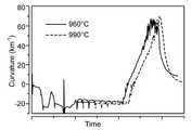
도 2a는 AlN 시드 층, AlGaN 버퍼 층들, AlN/GaN 초격자 구조 및 상단 GaN 층을 갖는 실리콘(Si) 기판을 나타내는 반도체 물질의 실시예의 개략적인 측면도이며, 도 2b는 상기 초격자 층들의 성장 동안의 웨이퍼 곡률 및 대응하는 곡률의 도식적인 표현이다.
도 3a는 특히 5×5 평방 마이크로미터 AFM 스캔으로의 Si 상의 AlN/GaN 초격자 구조 상부의 GaN 층의 현미경 사진이고, 도 3b는 특히 20×20 평방 마이크로미터 AFM 스캔으로의 Si 기판 상의 AlN/GaN 초격자 구조 상부의 GaN의 현미경 사진이며, 도 3c는 RT 웨이퍼 보우의 도식적인 표현이고, 도 3d는 GaN (004) 피크를 따른 3축 오메가-2 세타 스캔의 도식적인 표현이다.
도 4a는 Si 기판 상의 AlN/GaN 초격자 구조 상부의 GaN의 단면 TEM 이미지의 현미경 사진이며, 도 4b는 도 4a의 초격자 구조의 확대된 단면 이미지이다.
도 5a는 GaN 및 AlN 층들의 성장 동안에 각기 압축 및 인장 응력을 나타내는 초격자 층들의 개략적인 측면도이며, 도 5b는 초격자 층들의 성장 동안의 예시적인 곡률 진전의 도식적인 표현이다.
도 6a는 웨이퍼 곡률에 대한 변화되는 GaN 초격자 층들의 두께의 효과의 도식적인 표현이며, 도 6b는 웨이퍼 곡률에 대한 AlN 초격자 층들의 변화되는 두께의 효과의 도식적인 표현이다.
도 7a는 웨이퍼 응력에 대한 GaN 초격자 층들의 성장 조건들의 효과의 도식적인 표현이고, 도 7b는 웨이퍼 응력에 대한 AlN 초격자 층들의 V/III 비율들의 효과들의 도식적인 표현이며, 도 7c는 웨이퍼 응력에 대한 초격자 층들의 성장 온도의 효과들의 도식적인 표현이다.FIG. 1A is a schematic side view of an exemplary semiconductor material having a substrate and a superlattice structure for stress control, and FIG. 1B illustrates another exemplary semiconductor material having a substrate and a superlattice structure for stress control.
2A is a schematic side view of an embodiment of a semiconductor material showing a silicon (Si) substrate with an AlN seed layer, AlGaN buffer layers, an AlN / GaN superlattice structure and a top GaN layer, ≪ / RTI > is a graphical representation of the wafer curvature and corresponding curvature of the wafer.
Figure 3a is a micrograph of a GaN layer on top of an AlN / GaN superlattice structure, especially on a 5x5 square micrometer AFM scan, Figure 3b is a micrograph of an AlN / GaN superlattice structure on a Si substrate with a 20x20 square micrometer AFM scan, 3C is a schematic representation of the RT wafer bow and FIG. 3D is a graphical representation of a 3-axis OMEGA-2 theta scan along the GaN (004) peak.
4A is a micrograph of a cross-sectional TEM image of GaN on top of an AlN / GaN superlattice structure on a Si substrate, and FIG. 4B is an enlarged cross-sectional image of the superlattice structure of FIG. 4A.
FIG. 5A is a schematic side view of superlattice layers exhibiting compressive and tensile stresses during growth of GaN and AlN layers, and FIG. 5B is a graphical representation of an exemplary curvature evolution during growth of superlattice layers. FIG.
6A is a graphical representation of the effect of varying thickness of GaN superlattice layers on wafer curvature and FIG. 6B is a graphical representation of the effect of varying thickness of AlN superlattice layers on wafer curvature.
7A is a graphical representation of the effects of growth conditions of GaN superlattice layers on wafer stress, FIG. 7B is a graphical representation of the effects of V / III ratios of AlN superlattice layers on wafer stress, and FIG. Is a graphical representation of the effects of the growth temperature of the superlattice layers on stress.
본 발명은 웨이퍼 내의 다양한 층들의 인장 응력(tensile stress) 및 압축 응력(compressive stress)에 대응하도록 초격자 구조(superlattice structure)를 이용하는 상기 웨이퍼 내의 응력 제어에 관한 것이다.The present invention relates to stress control in a wafer utilizing a superlattice structure to correspond to the tensile and compressive stresses of the various layers within the wafer.
다음의 상세한 설명에 있어서, 그 일부를 구성하고 적어도 하나의 특정한 실시예가 예시를 통해 도시되는 첨부된 도면들을 참조한다. 다음의 상세한 설명은 추가적인 특정한 실시예들을 제공한다. 다른 실시예들도 고려되며, 본 발명의 범주나 사상으로부터 벗어나지 않고 구현될 수 있는 점이 이해되어야 할 것이다. 다음의 상세한 설명은 이에 따라 한정적인 의미로 기술되는 것은 아니다. 본 발명은 이와 같이 제한되지 않으면서도, 본 발명의 다양한 측면들의 이해는 다음에 제공되는 예들에 대한 설명을 통해 얻어질 것이다.In the following detailed description, reference is made to the accompanying drawings that form a part hereof, and in which is shown by way of illustration at least one specific embodiment. The following detailed description provides additional specific embodiments. It is to be understood that other embodiments are contemplated and may be implemented without departing from the scope or spirit of the invention. The following detailed description is, therefore, not to be construed in a limiting sense. While the invention is not so limited, an understanding of the various aspects of the invention will be gained through the description of the examples provided below.
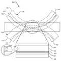
도 1a는 그 상단 상에 시드 층(121)을 구비하는 베이스 기판(102)을 포함하는 반도체 물질(100)을 도시한다. 도 1a는 또한 점선으로 볼록한(convex) 반도체 물질(104) 및 오목한(concave) 반도체 물질(106)을 도시한다. 상기 기판(102)의 격자 상수와 부정합(mismatch)되는 격자 상수를 가지는 버퍼(buffer) 구조(114)가 상기 기판(102) 및 상기 시드 층(121) 상에 형성될 때, 상기 버퍼 구조(114)는 이와 연관된 인장 응력을 가지며, 이는 상기 버퍼 구조(114) 및 상기 기판(102)/시드 층(121)이 비틀리고 볼록한 형태로 구부러지게 하여, 볼록한 반도체 물질(104)의 결과로 된다. 상기 버퍼 구조(114)보다 큰 격자 상수를 가지는 캡(cap) 층(116)이 상기 버퍼 구조(114) 상에 형성될 때, 상기 캡 층(116)은 이와 연관된 압축 응력을 가지며, 이는 전체적인 구조가 비틀리고 오목한 형태로 구부러지게 하여, 오목한 반도체 물질(106)의 결과로 된다. 이러한 구부러짐과 비틀림을 억제하기 위해, 초격자 구조가 상기 버퍼 구조(114) 및 상기 캡 층(116) 사이에 제공된다. 일부 예들에서, 상기 버퍼 구조는 선택적이며, 상기 초격자 구조가 상기 시드 층(121) 상에 직접 존재한다.1A shows a
도 1a는 또한 초격자 구조가 상기 구성 내에 제공될 때의 상기 기판(102)을 도시한다. 상기 기판(102)은 또한 상기 시드 층(121) 상의 버퍼 구조(122)를 구비하여 도시되며, 상기 버퍼 구조(122)는 상기 기판(102)의 격자와 정합되지 않는 격자 상수를 가진다. 상기 버퍼 구조(122) 상에 다른 격자 상수들을 갖는 물질들의 교번되는 층들로 이루어지는 초격자 구조(123)가 형성된다. 상기 초격자 구조(123)의 교번되는 층들은 압축 응력 및 인장 응력의 교번되는 층들을 가져온다. 상기 초격자 구조(123) 상에 상기 초격자 구조(123)의 격자 상수와 정합되는 격자 상수를 가지는 캡 층(124)이 형성된다. 상기 버퍼 구조(122), 상기 초격자 구조(123) 및 상기 캡 층(124)은 함께 내부의 응력들에 대응하며, 평탄한 반도체 물질(100)의 결과로 된다.Figure 1A also shows the
실리콘(Si) 기판들 상에 성장되는 AlGaN 기반의 고전자 이동도 트랜지스터(HEMT)들은 낮은 비용, 큰 직경의 기판들 및 Si 기반의 기술들과의 통합에 대한 잠재성에 대한 유용성으로 인해 상당한 연구 노력들이 집중되고 있다. 그러나, Si {111} 상의 GaN의 에피택시(epitaxy)는 공융 Ga-Si 반응들과 GaN 및 Si 사이의 격자 상수 및 열팽창 계수(CTE)의 큰 부정합으로 인하여 까다롭다. 도 1a에 도시한 바와 같이, 이러한 큰 격자 부정합은 성장 동안에 큰 웨이퍼 보우(bow)를 야기하는 상당한 내성 응력(intrinsic stress)과 함께 에피(epi)-층들 내의 높은 밀도의 불일치 및 관통 전위(threading dislocation)들을 가져올 수 있으며, 이는 결국 에피-층 두께, 합금 조성 및 장치 성능의 불균일성을 야기하는 상기 웨이퍼에 걸친 성장 온도의 큰 구배를 가져올 수 있다.AlGaN-based high electron mobility transistors (HEMTs) grown on silicon (Si) substrates suffer from significant research efforts due to their potential for low cost, large diameter substrates and integration with Si-based technologies Are concentrated. However, the epitaxy of GaN on Si {111} is tricky due to the large mismatch of eutectic Ga-Si reactions and lattice constants and thermal expansion coefficient (CTE) between GaN and Si. As shown in FIG. 1A, this large lattice mismatch is accompanied by significant intrinsic stresses that cause large wafer bow during growth, as well as high density mismatches and threading dislocations in the epi-layers ), Which can result in large gradients of growth temperature over the wafer, resulting in non-uniformity of the epi-layer thickness, alloy composition and device performance.
압축 내성 응력이 웨이퍼를 식히는 동안에 야기되는 큰 열적 인장 응력을 보상하도록 에피택시 동안에 상기 GaN 층 내에 의도적으로 내재될 수 있다. 도 1a의 초격자 구조(123)와 같은 초격자 구조가 성장면 내에 압축 내성 응력을 구현하고 전위들을 필터링하는 데 효과적인 것으로 발견되었다. Intrinsic in the GaN layer during epitaxy may be intrinsic to compensate for the large thermal tensile stress that is caused during cooling of the wafer. A superlattice structure, such as the
상기 초격자 구조(123)의 확대된 도면이 도 1a의 삽도에 도시된다. 상기 초격자 구조(123)는 교번되는 다른 격자 상수들을 갖는 물질들의 층들을 가지며; 특히, 도시된 초격자 구조(123)는 제2 물질층(132)과 교번되는 제1 물질층(131)을 가진다. 일부 실시예들에 있어서, 제1 물질층들(131)의 숫자는 제2 물질층들(132)의 숫자와 동일하지만, 다른 실시예들에서는 하나 또는 그 이상의 층을 가지는 것이 된다.An enlarged view of the
상기 제1 물질층(131) 및 상기 제2 물질층(132)은 각기 격자 상수를 가진다. 상기 격자 상수들의 하나는 다른 하나보다 크다. 즉, 상기 제1 물질층(131)이 상기 제2 물질층(132)보다 큰 격자 상수를 가지거나, 상기 제2 물질층(132)이 상기 제1 물질층(131)보다 큰 격자 상수를 가진다. 일부 실시예들에 있어서, 상기 격자 상수들 사이의 차이는 적어도 0.01Å, 또는 적어도 0.05Å, 또는 적어도 0.06Å, 또는 적어도 0.07Å, 또는 적어도 0.08Å이다.The
상기 제1 물질층(131) 및 상기 제2 물질층(132)은 상기 초격자 구조(123) 내에 교번되는 층들로 발견되며, 적어도 한 쌍의 교번되는 층들(131, 132)이 존재한다. 일부 실시예들에 있어서, 적어도 50쌍의 층들, 예를 들면, 약 50쌍 내지 100쌍의 층들이 존재한다. 다른 실시예들에 있어서, 보다 많거나 보다 적은 쌍들의 층들이 존재한다. 나타낸 바와 같이, 상기 층들(131, 132)은 쌍들로서나 하나의 층에 더해지는 쌍들로서 존재할 수 있다.The
각 물질층(131, 132)은 두께를 가진다. 비록 보다 얇거나 및/또는 보다 두꺼운 층들이 이용될 수 있지만, 예시적인 두께는 3㎚로부터 30㎚를 포함한다. 일부 실시예들에 있어서, 상기 제1 물질층(131) 및 상기 제2 물질층(132)은 동일한 두께는 가지지만, 다른 실시예들에서 상기 층들(131, 132)의 하나가 다른 하나보다 두껍다. 보다 두꺼운 층은 다른 층들보다, 예를 들면, 적어도 3㎚, 또는 적어도 5㎚, 또는 적어도 10㎚ 두꺼울 수 있다. 일부 실시예들에 있어서, 보다 두꺼운 층은 다른 층들보다 적어도 2배 두껍거나, 적어도 3배 두껍거나, 적어도 4배 두껍다. 상기 두 층들(131, 132)의 두께들 사이의 비는, 예를 들면, 1:2 내지 1:10이 될 수 있다.Each
GaN 및 Si 사이의 격자 상수 및 열팽창 계수(CTE)의 큰 부정합 때문에 실리콘 기판 상의 GaN 캡 층이 상기 내성 응력으로 인해 휘어지거나 구부러진 웨이퍼의 결과가 되게 한다. Al, Ga 및/또는 N 중의 임의의 것이나 모두(예를 들면, GaN 및 AlN)로 구성되는 교대되는 층들로 형성되는 초격자 구조가 상기 응력에 대향하여, 평탄한 반도체 물질을 가져온다.Due to the large mismatch of lattice constants and CTE between GaN and Si, the GaN cap layer on the silicon substrate may result in warped or bent wafers due to this stress tolerance. A superlattice structure formed of alternating layers of any of Al, Ga and / or N (e.g., GaN and AlN), is against this stress, resulting in a flat semiconductor material.
상기 초격자 구조 내의 개별적인 층들의 예시적인 두께는 3㎚―35㎚와 같이 1㎚―50㎚이다. GaN 및 AlN 물질들에 대하여, 상기 층들의 예시적인 두께는 AlN에 대해 3㎚―5㎚이고 and GaN에 대해 10㎚―30㎚이다. GaN은 has 3.19Å의 격자 상수를 가지고, AlN은 3.11Å의 격자 상수를 가지며, 이는 압축 응력을 갖는 상기 GaN 층 및 인장 응력을 갖는 상기 AlN 층을 가져온다.The exemplary thickness of the individual layers in the superlattice structure is 1 nm-50 nm, such as 3 nm-35 nm. For GaN and AlN materials, the exemplary thickness of the layers is between 3 nm and 5 nm for AlN and between 10 nm and 30 nm for and GaN. GaN has a lattice constant of 3.19A and AlN has a lattice constant of 3.11A which results in the GaN layer with compressive stress and the AlN layer with tensile stress.
일 실시예에 있어서, 본 발명은 실리콘(Si) 기판, 상기 Si 기판 상의 AlN 시드 층, 다중의 AlxGa1-xN 층들로 구성되는 버퍼 구조(여기서 0≤x≤1이다), 상기 버퍼 구조 상에 형성되는 적어도 한 쌍의 AlN 및 GaN 층들을 구비하는 초격자(SL) 구조, 그리고 상기 SL 구조 상에 형성되는 캡 층(예를 들면, GaN)으로 형성되는 반도체 물질을 제공한다. 상기 SL 구조는 50쌍―100쌍의 AlN/GaN 층들을 가지며, 개개의 층 두께는 AlN에 대해 3㎚―5㎚이고, GaN에 대해 10㎚―30㎚이다. 다른 특정한 실시예에 있어서, 상기 SL 구조는 50쌍―100쌍의 AlN/GaN 및 하나의 추가적인 GaN 층을 가진다.In one embodiment, the present invention provides a buffer structure comprising a silicon (Si) substrate, an AlN seed layer on the Si substrate, multiple Alx Ga1-x N layers (where 0? X? 1) A superlattice (SL) structure having at least a pair of AlN and GaN layers formed on the structure, and a cap layer (e.g., GaN) formed on the SL structure. The SL structure has 50 pairs of -100 pairs of AlN / GaN layers, and the individual layer thickness is 3nm-5nm for AlN and 10nm-30nm for GaN. In another particular embodiment, the SL structure has 50 pairs of -100 pairs of AlN / GaN and one additional GaN layer.
비록 상기 Si 기판 상의 AlN 시드 층이 앞서 기술되고 다음에 더 설명되지만, 상기 시드 층은 Al, Ga 및/또는 N 중의 임의의 것으로 구성될 수 있으며, 상기 버퍼 구조 및/또는 상기 초격자 구조에 따라 선택된다. 일부 실시예들에 있어서, 상기 시드 층은 상기 Si 기판과 격자 부정합된다. 유사하게, 비록 다중의 층들의 AlxGa1-xN 층들(여기서 0≤x≤1이다)로 구성되는 버퍼 구조가 앞서 기술되고 다음에 더 설명되지만, 상기 버퍼 구조는 Al, Ga 및/또는 N 중의 임의의 것으로 구성될 수 있으며, 상기 시드 층 및/또는 상기 초격자 구조에 따라 선택된다. 일부 실시예들에 있어서, 상기 버퍼 구조는 상기 Si 기판과 격자 부정합된다.Although the AlN seed layer on the Si substrate is described above and described further below, the seed layer may be comprised of any of Al, Ga, and / or N, and may be formed in accordance with the buffer structure and / or the superlattice structure Is selected. In some embodiments, the seed layer is lattice mismatched with the Si substrate. Similarly, although a buffer structure consisting of Alx Ga1-x N layers (where 0? X? 1) of multiple layers is described above and described further below, the buffer structure may comprise Al, Ga and / N, and is selected according to the seed layer and / or the superlattice structure. In some embodiments, the buffer structure is lattice mismatched with the Si substrate.
도 1b에서, 반도체 물질의 다른 실시예가 제공된다. 반도체 물질(200)은 시드 층(221)이 상부에 있는 베이스 기판(202)을 가진다. 상기 시드 층(221)의 상단에 선택적이 될 수 있는 버퍼 구조(222)가 있다. 상기 버퍼 구조(222)는 다중(예를 들면, 셋 또는 그 이상의) AlxGa1-xN 층들로 구성되며, 여기서 0≤x≤1 또는 0<x<1이다. Al 및 Ga의 비율은 상기 다중의 층들 사이에서 상이하며, 내부에 Al이 보다 큰 층들이 상기 시드 층(221)에 인접하고, 내부에 Ga가 보다 큰 층들이 상기 초격자 구조(223)에 인접한다.In Figure 1b, another embodiment of a semiconductor material is provided.
상기 초격자 구조(223)는 (a) GaN 및 (b) AlN, AlyGa1-yN(여기서 0<y<1이다) 및 이들의 혼합물들로 이루어진 그룹으로부터 선택되는 층들인 복수의 층들(231, 232, 233)을을 가진다. 상기 층들은 임의의 순서로 배치될 수 있다. 따라서, 일 예에서, 상기 층들(231, 232, 233)은 각기 AlyGa1-yN/AlN/GaN이 될 수 있다. 다른 예에서, 상기 층들(231, 232, 233)은 AlN/AlyGa1-yN/GaN이 될 수 있다. GaN, AlN 및 AlyGa1-yN의 다른 층 형성도 가능하다. 층들의 숫자는 상기 기판 특성들에 따라 일부 실시예들에서 적어도 50세트의 층들(하나의 세트가 임의의 순서로 각각의 GaN/AlN/AlyGa1-yN의 하나의 층인 것을 의미함), 예를 들면, 50세트 100세트의 층들을 가지는 것으로 변화될 수 있지만, 다른 실시예들에서는 보다 많거나 보다 적은 세트의 층들이 존재할 수 있다.The superlattice structure 223 (a), GaN, and (b) AlN, Aly Ga1-y N (where 0 <y <1 a) and a plurality of layers, which are layer is selected from the group consisting of a mixture thereof (231, 232, 233). The layers may be arranged in any order. Thus, in one example, the
변화되는 양의 Al 및 Ga를 가지는 AlyGa1-yN을 구비하는 도 1a 및 도 1b의 예들 모두에 대해, 상기 AlGaN에 대한 격자 상수는 상기 AlN 및 GaN의 격자 상수들의 사이에 있을 것이다. 따라서, 성장되는 반도체 구조에 따라, 상기 AlGaN 층 내의 Al 및 Ga의 비율은 상기 반도체 구조 내에 필요한 층들의 세트들의 숫자에 따라 변화될 수 있거나, 일정하게 유지될 수 있거나, 이들의 조합이 될 수 있다. 다양한 층들인 AlGaN의 두께는 여기에 논의된 AlN 및 GaN 층들과 유사하며, 상기 AlGaN 층들의 두께는 대체로 상기 AlN 및 GaN 층들의 두께들 사이에 있다.For both of the examples of Figs. 1A and 1B with Aly Ga1-y N having Al and Ga of varying amounts, the lattice constant for the AlGaN will be between the lattice constants of the AlN and GaN. Thus, depending on the semiconductor structure being grown, the proportion of Al and Ga in the AlGaN layer may be varied, maintained constant, or a combination thereof, depending on the number of sets of layers required in the semiconductor structure . The thickness of the various layers, AlGaN, is similar to the AlN and GaN layers discussed herein, and the thickness of the AlGaN layers is generally between the thicknesses of the AlN and GaN layers.
여기서의 다른 실시예들과 같이, 캡 층(224)은 상기 초격자 구조(223)의 상단 상에 있다. 상기 캡 층(224)은 Al, Ga, N 중의 하나 또는 그 이상으로 이루어질 수 있다. 통상적인 실시예에 있어서, 상기 캡 층(224)은 GaN이 될 것이다. 다양한 반도체 장치들, 예를 들면, HEMT를 위한 다양한 액티브 층들이 이후에 상기 캡 층(224) 상에 성장될 수 있다.As in other embodiments herein, the
다양한 에피택시 공정 실험들이 최신의 비코 프로펠TM 파워(Veeco PropelTM Power) GaN MOCVD 시스템에서 수행되었으며, 이는 200㎜의 단일 웨이퍼 MOCVD 반응기를 포함한다. 상기 시스템은 웨이퍼 온도, 반사율 및 웨이퍼 곡률(curvature) 측정들을 위한 DRT-210 인-시튜(in-situ) 공정 모니터(통합 고온계-반사계-휨 측정계 유닛)를 구비하였다. 성장 응력의 진전이 상기 인-시튜 휨 측정계를 이용하여 웨이퍼 곡률의 변화를 통해 실시간으로 모니터되었다. AlN/GaN SL 층들과 함께 GaN의 에피택시가 도 2a에 도시한 바와 같이 200㎜의 초크랄스키(Czochralski: CZ) 축 상의 Si {111} 기판들 상에서 1.0㎜의 두께로 수행되었다. 크랙-프리(crack-free)의 2㎜ 두께의 벌크 GaN 캡 층들이 상기 SL 구조 상부에 형성되었고, 이는 AlN 시드 층 및 Al과 Ga의 다른 비율들을 갖는 다중의 AlxGa1-xN 층들(여기서 0<x<1이다)로 구성되는 버퍼 구조 상부에 있었으며, Al이 가장 큰 것이 상기 AlN 시드 층에 인접하였고, Ga가 가장 큰 것이 상기 SL 구조에 인접하였다. 예시적인 실시예에 있어서, 비록 다른 실시예들에서는 보다 많은 층들(예를 들면, 5개의 층들)이 존재하거나 및/또는 원소 분포가 다르지만, 상기 버퍼 구조는 Al0.75Ga0.25N, Al0.50Ga0.50N 및 Al0.25Ga0.75N의 층들로 구성되었다.Various epitaxy processes experiments have been carried out by the latest VicoTM propeller power (Veeco Propel PowerTM) GaN MOCVD system, which comprises a single wafer reactor of the
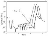
성장 동안의 웨이퍼 곡률의 진전의 예가 도 2b에 도시되며. 웨이퍼 곡률은 AlN/AlGaN 시드 층/버퍼 구조의 성장 동안에 상기 필름의 인장 응력으로 인하여 음이(오목한) 된다. 상기 시드 층 및 버퍼 구조의 성장 후, 곡률은 성장 시간에 대해 상기 AlN/GaN SL 층들의 두께와 함께 선형으로 변화되었다. 압축 응력은 상기 벌크 GaN 층의 성장 동안에 내재되며, 상기 곡률은 볼록한 웨이퍼 보우로 양이 된다. 이러한 볼록한 곡률은 상기 Si 및 성장된 에피-층들 사이의 CTE의 부정합으로부터 초래되는 큰 인장 응력으로 인하여 식히는 동안에 감소되었다.An example of the progression of wafer curvature during growth is shown in FIG. Wafer curvature is negative (concave) due to the tensile stress of the film during growth of the AlN / AlGaN seed layer / buffer structure. After growth of the seed layer and the buffer structure, the curvature changed linearly with the thickness of the AlN / GaN SL layers with respect to growth time. The compressive stress is inherent during the growth of the bulk GaN layer, and the curvature is positive with the convex wafer bow. This convex curvature was reduced during cooling due to the large tensile stress resulting from the mismatch of CTE between the Si and the grown epi-layers.
GaN 에피택셜 필름들의 결정질은 (002) 및 (102) 방향들을 따라 고해상도의 X-선 회절(HRXRD)을 이용하여 측정되었다. GaN (004) 방향을 따른 3축 결합 오메가(omega)-2 세타(theta) 스캔이 상기 SL들의 주기 두께 및 계면 조도(interface roughness)를 결정하는 데 이용되었다. 표면 모폴러지(morphology)는 원자간력 현미경(AFM)으로 연구되었으며, 샘플들의 단면들은 고해상도의 투과 전자현미경(TEM)으로 특성화되었다. 증착 후의 웨이퍼 보우는 실온에서의 웨이퍼 응력 측정으로 특성화되었다.Crystals of GaN epitaxial films were measured using high resolution X-ray diffraction (HRXRD) along the (002) and (102) directions. A three-axis coupled omega-2 theta scan along the GaN (004) direction was used to determine the periodic thickness and interface roughness of the SLs. Surface morphology was studied with atomic force microscopy (AFM), and sections of the samples were characterized by high resolution transmission electron microscopy (TEM). The wafer bow after deposition was characterized by measurement of wafer stress at room temperature.
두꺼운 GaN 캡 층이 상기 초격자 구조 스택(stack) 상부에 적용되었으며, 이러한 GaN 층은 적어도 1마이크로미터 두께였고, 일부 실시예들에서는 약 2마이크로미터 두께였다.A thick GaN cap layer was applied on top of the superlattice structure stack, which was at least 1 micrometer thick and, in some embodiments, about 2 micrometers thick.
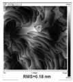
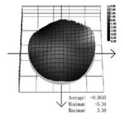
AlN/GaN SL 층들 상부의 2㎜의 스택 GaN에 대해, 매끄러운 표면들이 도 3a 및 도 3b에 도시한 바와 같이, 예를 들면, 5×5㎛2스캔 내의 0.18㎚ 및 예를 들면, 20×20㎛2스캔 내의 0.82㎚의 조도로 AFM으로 관찰되었다. AFM으로부터의 표면 피트(pit)들에 기초한 전위 밀도는 약 4×10⁻⁸/㎠이었다. 도 3b에 도시한 바와 같이, 실온(RT)에서의 웨이퍼 보우는 <±10㎜의 범위 이내였다. XRD 요동 곡선(rocking curve)들은 GaN {002} 및 {102}에 대해 각기 352arcsec 및 375arcsec의 FWHM을 나타내었다. GaN {004}를 따른 3축 결합 오메가-2 세타 스캔은 도 3c에서 도시한 바와 같이 +6th위성 피크(satellite peak)까지를 나타내며, 도 3c에 도시한 바와 같이 상기 AlN/GaN SL 층들에 대해 매끄러운 계면질을 나타낸다. 상기 주기 두께는 4㎚ AlN/17㎚ GaN from 상기 XRD 오메가-2 세타 스캔으로부터 4㎚ AlN/17㎚ GaN로 적합하게 되었다.For the stack of
AlN/GaN SL 층들이 상기 성장 방향을 따른 전위 필터링을 위해 효과적인 점이 발견되었다. 도 4a는 상기 SL들의 상단 부분을 향하는 관통 전위들의 종료를 나타내는 단면 TEM 이미지이다. 도 4b는 ~22㎚의 주기 두께를 가지는 AlN/GaN SL 층들의 확대된 도면을 나타낸다.It has been found that AlN / GaN SL layers are effective for potential filtering along the growth direction. 4A is a cross-sectional TEM image showing the termination of the threading dislocations towards the upper portion of the SLs. 4B shows an enlarged view of AlN / GaN SL layers having a period thickness of ~ 22 nm.
웨이퍼 응력에 대한 GaN 및 AlN 두께의 영향Effect of GaN and AlN Thickness on Wafer Stress
GaN 및 AlN 사이의 격자 상수의 차이로 인해, 상기 SL들 내의 GaN 및 AlN의 얇은 층들의 부정형 성장(pseudomorphic growth)이 상기 GaN 및 AlN 층들 내에 다른 응력 레벨들을 가져온다. AlN 층의 상단 상에 성장된 GaN 층의 경우, GaN은 AlN의 격자 상수(a=3.11Å)에 비해 이의 보다 큰 격자 상수(a=3.19Å)로 인하여 압축 응력을 겪을 것이다. 반대로, 도 5a에 예시한 바와 같이, AlN은 GaN 층의 상단 상에 성장될 때에 인장 응력을 가질 것이다. 상기 초격자 층들의 성장 동안, 상기 웨이퍼 곡률은 전체적인 응력이 개개의 AlN 및 GaN 층들로부터의 축적이므로 상기 초격자 층들의 쌍 두께의 증가와 함께 선형으로 변화된다. 도 5b에 도시한 바와 같이, 상기 곡률 증가의 기울기가 양일 경우, 상기 SL들의 전체적인 응력은 압축이고, 곡률 변화의 음의 기울기는 상기 구조 내의 인장 응력을 나타내며, 평탄한 기울기는 성장 온도에서 균형을 이룬 응력을 의미한다. 식힌 후의 상기 상단 GaN 층에 대한 최종 잔류 응력이 상기 SL들 내에 내재된 응력에 의해 영향을 받기 때문에, 상기 SL들 내의 주기성을 제어함에 의해 응력 조절이 가능해 진다.Due to the difference in lattice constants between GaN and AlN, pseudomorphic growth of thin layers of GaN and AlN in the SLs results in different stress levels in the GaN and AlN layers. For the GaN layer grown on top of the AlN layer, GaN will undergo compressive stress due to its larger lattice constant (a = 3.19 ANGSTROM) compared to the lattice constant of AlN (a = 3.11 ANGSTROM). Conversely, as illustrated in Fig. 5A, AlN will have tensile stress when grown on top of the GaN layer. During growth of the superlattice layers, the wafer curvature changes linearly with the increase in the pair thickness of the superlattice layers since the overall stress is accumulation from the individual AlN and GaN layers. As shown in FIG. 5B, when the slope of the curvature increase is positive, the overall stress of the SLs is compression, the negative slope of the curvature change indicates tensile stress in the structure, and the flat slope is balanced at the growth temperature Stress. Since the final residual stress for the upper GaN layer after cooling is affected by the stresses inherent in the SLs, stress control is enabled by controlling the periodicity in the SLs.
상기 AlN 및 GaN 층들의 두께를 조절함에 의해, 상기 초격자 구조의 응력이 이에 따라 제어될 수 있다. AlN 층에 대한 일정한 두께 및 증가하는 GaN 두께를 이용하는 것은 상기 초격자 구조 내에 보다 큰 압축 응력을 가져왔다. 도 6a에 예시한 바와 같이, 상기 웨이퍼 곡률의 기울기가 GaN 두께의 증가와 함께 증가되었으며, 상기 초격자 구조 내에 내재되는 보다 큰 압축 응력을 나타낸다. GaN의 일정한 두께에 대해, 도 6b에 도시한 바와 같이 AlN 두께의 감소는 보다 큰 압축 응력 및 곡률 변화의 증가된 속도를 가져왔다. 식힌 후에 웨이퍼 곡률/보우는 상기 초격자 구조 내로 구현된 응력 레벨에 의해 결정된다.By adjusting the thickness of the AlN and GaN layers, the stress of the superlattice structure can be controlled accordingly. Using a constant thickness and increasing GaN thickness for the AlN layer has resulted in greater compressive stresses in the superlattice structure. As illustrated in FIG. 6A, the slope of the wafer curvature is increased with increasing GaN thickness, and exhibits a greater compressive stress inherent in the superlattice structure. For a constant thickness of GaN, a decrease in AlN thickness, as shown in Figure 6b, resulted in greater compressive stress and increased speed of curvature change. The wafer curvature / bow after cooling is determined by the stress level implemented in the superlattice structure.
웨이퍼 응력에 대한 성장 조건들의 영향Effect of Growth Conditions on Wafer Stress
[029] 일정한 주기 두께에서, 상기 GaN 및 AlN의 성장 조건들은 상기 SL들 내의 응력에 영향을 미친다. 도 7a는 상기 GaN 층의 다른 성장 속도(GR)들을 갖는 상기 초격자 구조의 곡률 진전을 나타낸다. GaN의 성장 속도가 40㎚/min 내지 65㎚/min로 증가함에 따라, 보다 큰 압축 응력이 구현되는 경향이 있었다. 실험은 17㎚의 일정한 GaN 두께에서 수행되었다. 경향은 반전되었고, GaN GR을 to 90㎚/min까지 더 증가시킴에 의해 인장 응력이 구현되기 시작하였다. 300mmol/min의 일정한 TMAl 흐름에서, 상기 AlN의 성장 속도는 보다 낮은 NH3또는 V/III 비율과 함께 증가되었다. 상기 초격자 구조 내의 AlN 및 GaN 모두에 대한 일정한 주기 두께에서, 도 7b에 도식화한 바와 같이 보다 큰 압축 응력이 상기 V/III 비율을 낮춤(보다 높은 AlN 성장 속도)에 의해 구현되었다.[029] At constant period thickness, the growth conditions of GaN and AlN affect the stress in the SLs. Figure 7a shows the curvature evolution of the superlattice structure with different growth rates (GR) of the GaN layer. As the growth rate of GaN increases from 40 nm / min to 65 nm / min, a larger compressive stress tends to be realized. The experiment was performed at a constant GaN thickness of 17 nm. The tendency was reversed and tensile stress began to be realized by further increasing the GaN GR to 90 nm / min. In certain TMAl flow of 300mmol / min, the growth rate of the AlN is increased with lower NH3 or the V / III ratio. At constant period thicknesses for both AlN and GaN in the superlattice structure, greater compressive stress as illustrated in Figure 7b was achieved by lowering the V / III ratio (higher AlN growth rate).
성장 온도의 효과는 상기 Si 표면 상의 고온계로 측정하면서 960℃ 내지 990℃에서 테스트되었다. 성장 속도들은 감소되는 성장 온도와 함께 증가되었다. 성장 시간을 조절하고, 일정한 주기 두께를 유지함에 의해, 초격자 구조의 응력 내의 상당한 차이는 테스트된 온도 범위 이내에서 관찰되지 않았다.The effect of growth temperature was tested at 960 캜 to 990 캜 while being measured with a pyrometer on the Si surface. Growth rates were increased with decreasing growth temperature. By adjusting the growth time and maintaining a constant period thickness, significant differences in the stresses of the superlattice structure were not observed within the tested temperature range.
앞서의 기재는 상기 구조와 본 발명의 예시적인 실시예들의 완전한 설명을 제공한다. 앞서의 설명은 특정한 실시예들을 제공한다. 다른 실시예들도 고려되며, 본 발명의 범주와 사상을 벗어나지 않고 구현될 수 있는 점이 이해될 것이다.The foregoing description provides a complete description of the above structure and exemplary embodiments of the invention. The foregoing description provides specific embodiments. It will be appreciated that other embodiments are contemplated and may be implemented without departing from the scope and spirit of the invention.
예를 들면, 실리콘(Si) {111} 이외의 다른 베이스 기판들이 사용될 수 있다. 대체로, 상기 베이스 웨이퍼 및 상기 초격자 구조는 부정합을 가진다. 임의의 시드 층이 사용될 수 있지만, 통상적으로는 상기 베이스 기판과 부정합된다.For example, base substrates other than silicon (Si) {111} may be used. In general, the base wafer and the superlattice structure have mismatches. Any seed layer can be used, but is typically mismatched with the base substrate.
AlN 및 GaN 이외의 초격자 층 물질들이 사용될 수 있고, 임의의 첨가제들이나 도펀트들이 포함될 수 있다. 상기 두 초격자 층 물질들의 격자 상수들은 0.01Å만큼 작게 다를 수 있거나, 상기 두 격자 상수들이 1% 또는 2%만큼 작게 다를 수 있다 상기 초격자 층들의 두께는 어느 범위, 예를 들면, 1㎚ 내지 50㎚가 될 수 있다. 통상적으로, 상기 초격자 물질층들의 하나는 비록 이러한 사양이 요구되지는 않지만 다른 하나보다 두껍게 될 것이다. 앞서 제공되는 특정한 실시예에 대해, 비록 다른 실시예들에서는 보다 작은 격자 상수를 갖는 물질이 보다 두꺼운 층이 될 수 있지만, 보다 큰 격자 상수를 갖는 물질(이에 따라 상기 초격자 구조에 압축 응력을 생성한다)이 보다 두꺼운 층이 된다. 상기 초격자 층들은 대체로 쌍들(즉, 각 물질의 층에 대해 다른 물질의 하나의 층이 존재한다)로서 존재하지만, 일부 실시예들에서, 상기 초격자 물질들의 하나의 보다 많은 층들이 존재할 수 있다. 일부 실시예들에 있어서, 상기 초격자 구조는 존재하는 제3 물질을 가질 수 있다. 상기 제3 물질은, 예를 들면, 압축 응력, 인장 응력, 또는 중립을 제공할 수 있다. 임의의 제3 층은 임의의 방식으로, 예를 들면, A-B-C-A-B-C…, A-B-C-B-A-B-C-B-A,… 등으로 다른 초격자 층들과 교번될 수 있다. 상기 초격자 구조의 다른 변형들도 사용 가능하다.Superlattice layer materials other than AlN and GaN may be used, and any additives or dopants may be included. The lattice constants of the two superlattice layer materials may be as small as 0.01 Angstroms, or the two lattice constants may be as small as 1% or 2%. The thickness of the superlattice layers may be any range, for example, 50 nm. Typically, one of the layers of superlattice material will be thicker than the other, although such a specification is not required. For certain embodiments provided earlier, although in other embodiments the material with a smaller lattice constant can be a thicker layer, a material with a larger lattice constant (thus producing a compressive stress in the superlattice structure ) Becomes a thicker layer. The superlattice layers are generally in pairs (i. E., There is one layer of different material for each layer of material), but in some embodiments one more layer of the superlattice materials may be present . In some embodiments, the superlattice structure may have an existing third material. The third material may provide, for example, compressive stress, tensile stress, or neutrality. Any third layer may be formed in any manner, for example, ABCDAB, , A-B-C-B-A-B-C-B-A, May alternate with other superlattice layers. Other variations of the superlattice structure are available.
앞서의 상세한 설명은 이에 따라 제한적인 의미로 이해되는 것은 아니다. 본 발명은 이와 같이 제한되지는 않지만, 본 발명의 다양한 측면들의 이해가 제공되는 예들의 논의를 통해 얻어질 것이다.The foregoing detailed description is therefore not to be taken in a limiting sense. While the present invention is not so limited, an understanding of the various aspects of the present invention will be gained through discussion of examples provided.
달리 기술하지 않는 한, 특징 크기들, 양들 및 물리적 성질들을 나타내는 모든 숫자들은 "약"이라는 용어로 변될 수 있는 것으로 이해되어야 한다. 이에 따라, 달리 나타내지 않는 한, 설시되는 임의의 수치 변수들은 여기에 개시되는 기술들을 활용하는 해당 기술 분야의 숙련자에 의해 도출될 수 있는 원하는 성질들에 따라 변화될 수 있는 근사치들이다.Unless otherwise stated, all numbers expressing feature sizes, quantities, and physical properties are to be understood as being modified to the term "about ". Accordingly, unless indicated to the contrary, any numerical parameter set forth is an approximation that may be varied according to desired properties that may be derived by those skilled in the art utilizing the techniques disclosed herein.
여기에 사용되는 바에 있어서, "일", "하나" 및 "상기"의 단수 형태들은 여기서 명백하게 달리 기재되지 않는 한, 복수의 지시 대상들을 가지는 실시예들을 포괄한다. 본 명세서와 첨부된 특허청구범위에서 사용되는 바와 같이, "또는"이라는 용어는 명백하게 달리 기재되지 않는 한 대체로 "및/또는"을 포함하는 의미로 사용된다.As used herein, the singular forms "one," "one, " and" the "encompass embodiments having a plurality of directives, unless expressly stated otherwise herein. As used in this specification and the appended claims, the term "or" is generally used in its sense including "and / or" unless explicitly stated otherwise.
이에 한정되는 것은 아니지만, "하단", "하부", "상단", "상부", "하부에", "아래에", "상부에", "상단 상에", "상에" 등을 포함하는 공간적으로 관련되는 용어들은, 여기서 사용되는 경우에 다른 것들에 대한 요소(들)의 공간적인 관련성을 기술하는 설명의 용이성을 위해 사용된다. 이러한 공간적으로 관련되는 용어들은 장치의 다른 배향들 이외에도 도면들에 도시되고 여기에 설명되는 특정한 배향들을 포괄한다. 예를 들면, 도면들에 나타낸 구조가 반전되거나 뒤집히는 경우, 다른 요소들의 아래 또는 하부인 것으로 이전에 설명되는 부분들이 이들 다른 요소들의 상부 또는 상에 있을 수 있다.But are not limited to, "lower," "lower," "upper," "upper," "lower," "lower," "upper," "upper," " Spatially related terms used herein are used for ease of description to describe the spatial relevance of the element (s) to others when used herein. These spatially related terms encompass the specific orientations shown in the drawings and described herein, as well as other orientations of the device. For example, where the structure shown in the figures is inverted or inverted, portions previously described as being below or below other elements may be on or above these other elements.
본 발명의 많은 실시예들이 본 발명의 사상과 범주를 벗어나지 않고 구현될 수 있으므로, 본 발명은 다음에 첨부되는 특허청구범위에 나타난다. 또한, 다른 실시예들의 구조적인 특징들은 다음의 특허청구범위로부터 벗어나지 않고 또 다른 실시예에서 결합될 수 있다.Since many embodiments of the present invention can be implemented without departing from the spirit and scope of the invention, the present invention is indicated in the claims appended hereto. Further, structural features of other embodiments may be combined in yet another embodiment without departing from the scope of the following claims.
Claims (26)
Translated fromKorean기판을 포함하고;
상기 기판 상의 시드 층을 포함하며;
상기 시드 층 상의 초격자 구조(superlattice structure)를 포함하고, 상기 초격자 구조는 (a) 갈륨 질화물(GaN) 및 (b) 알루미늄 질화물(AlN), AlyGa1-yN(여기서 0<y<1이다) 및 이들의 혼합물들로 이루어진 그룹으로부터 선택되는 층들의 복수의 초격자 층들을 포함하며, 상기 초격자 층들은 임의의 순서로 배치되고;
상기 초격자 구조 상에 형성되는 캡(cap) 층을 포함하는 것을 특징으로 하는 반도체 물질.In a semiconductor material,
A substrate;
A seed layer on said substrate;
And a superlattice structure on the seed layer, wherein the superlattice structure comprises (a) gallium nitride (GaN) and (b) aluminum nitride (AlN), Aly Ga1-y N, ≪ 1), and mixtures thereof, wherein the superlattice layers are arranged in any order;
And a cap layer formed on the superlattice structure.
실리콘(Si) 기판을 필수적으로 포함하고;
상기 Si 기판 상의 AlN 시드 층을 필수적으로 포함하며;
상기 시드 층 상의 버퍼 구조를 필수적으로 포함하고, 상기 버퍼 구조는 셋 또는 그 이상의 별개의 AlxGa1-xN(여기서 0<x<1이다)의 층들을 포함하며;
상기 버퍼 구조 상의 초격자 구조를 필수적으로 포함하고, 상기 초격자 구조는 (a) 갈륨 질화물(GaN) 및 (b) 알루미늄 질화물(AlN), AlyGa1-yN(여기서 0<y<1이다) 및 이들의 혼합물들로 이루어진 그룹으로부터 선택되는 층들의 임의의 순서의 복수의 층들을 포함하며;
상기 초격자 구조 상에 형성되는 캡 층을 필수적으로 포함하는 것을 특징으로 하는 반도체 물질.The method according to claim 1,
A silicon (Si) substrate;
An AlN seed layer on the Si substrate;
Wherein the buffer structure essentially comprises layers of three or more discrete Alx Ga1-x N (where 0 < x <1);
Wherein the superlattice structure on the buffer structure essentially comprises (a) gallium nitride (GaN) and (b) aluminum nitride (AlN), Aly Ga1-y N, where 0 &≪ / RTI > and mixtures thereof; and < RTI ID = 0.0 > a < / RTI >
And a cap layer formed on the superlattice structure.
각각의 상기 초격자 층들은 Al, Ga, N 중의 하나 또는 그 이상을 포함하고, 상기 복수의 초격자 층들의 적어도 하나는 압축 응력(compressive stress)을 제공하며, 상기 복수의 초격자 층들의 적어도 하나는 인장 응력(tensile stress)을 제공하고;
상기 캡 층은 Al, Ga, N 중의 하나 또는 그 이상을 포함하며, 상기 초격자 구조와 격자 정합되는 것을 특징으로 하는 반도체 물질.The method according to claim 1,
Wherein each of said superlattice layers comprises one or more of Al, Ga, N, at least one of said plurality of superlattice layers providing a compressive stress, and at least one of said plurality of superlattice layers Provides tensile stress;
Wherein the cap layer comprises one or more of Al, Ga, N and is lattice matched to the superlattice structure.
Applications Claiming Priority (3)
| Application Number | Priority Date | Filing Date | Title |
|---|---|---|---|
| US14/729,741 | 2015-06-03 | ||
| US14/729,741US20160359004A1 (en) | 2015-06-03 | 2015-06-03 | Stress control for heteroepitaxy |
| PCT/US2016/032969WO2016196007A1 (en) | 2015-06-03 | 2016-05-18 | Stress control for heteroepitaxy |
Publications (1)
| Publication Number | Publication Date |
|---|---|
| KR20180014729Atrue KR20180014729A (en) | 2018-02-09 |
Family
ID=57442107
Family Applications (1)
| Application Number | Title | Priority Date | Filing Date |
|---|---|---|---|
| KR1020177036030AWithdrawnKR20180014729A (en) | 2015-06-03 | 2016-05-18 | Stress Control for Heteroepitaxy |
Country Status (7)
| Country | Link |
|---|---|
| US (1) | US20160359004A1 (en) |
| EP (1) | EP3295474A4 (en) |
| JP (1) | JP2018520499A (en) |
| KR (1) | KR20180014729A (en) |
| CN (1) | CN107810544A (en) |
| TW (1) | TW201705215A (en) |
| WO (1) | WO2016196007A1 (en) |
Families Citing this family (15)
| Publication number | Priority date | Publication date | Assignee | Title |
|---|---|---|---|---|
| US9570300B1 (en)* | 2016-02-08 | 2017-02-14 | International Business Machines Corporation | Strain relaxed buffer layers with virtually defect free regions |
| JP7158842B2 (en)* | 2017-01-23 | 2022-10-24 | アイメック・ヴェーゼットウェー | III-N substrate for power electronics device and manufacturing method thereof |
| US20200083075A1 (en)* | 2018-09-06 | 2020-03-12 | Veeco Instruments Inc. | System and method for metrology using multiple measurement techniques |
| WO2020149729A1 (en)* | 2019-01-17 | 2020-07-23 | Collaborative Research In Engineering, Science And Technology Center | A method for growing a non-polar a-plane gallium nitride using aluminum nitride / gallium nitride superlattices |
| US20220090294A1 (en)* | 2019-01-17 | 2022-03-24 | Collaborative Research In Engineering, Science And Technology Center | Method for growing a semi-polar gallium nitride epitaxial layer using aluminum nitride / gallium nitride superlattices |
| JP7132156B2 (en) | 2019-03-07 | 2022-09-06 | 株式会社東芝 | semiconductor equipment |
| CN110783176B (en)* | 2019-10-30 | 2022-07-12 | 广西大学 | Preparation method of low-stress semiconductor material |
| CN111682093A (en)* | 2020-06-16 | 2020-09-18 | 璨隆科技发展有限公司 | A kind of gallium nitride epitaxial chip and preparation method thereof |
| CN111628060A (en)* | 2020-06-16 | 2020-09-04 | 璨隆科技发展有限公司 | Gallium nitride epitaxial chip and preparation method thereof |
| CN112117344B (en)* | 2020-09-23 | 2022-05-31 | 扬州乾照光电有限公司 | A solar cell and method of making the same |
| CN112670164B (en)* | 2020-12-24 | 2023-01-24 | 南京百识电子科技有限公司 | Growth method of superlattice on epitaxial bottom layer of gallium nitride |
| KR102734493B1 (en)* | 2021-05-28 | 2024-11-27 | 주식회사 아이브이웍스 | Ⅲ-N semiconductor structure and method of manufacturing the same |
| CN116264243A (en)* | 2021-12-15 | 2023-06-16 | 苏州能讯高能半导体有限公司 | Epitaxial structure of semiconductor device, preparation method of epitaxial structure and semiconductor device |
| CN118016710B (en)* | 2024-04-10 | 2024-07-02 | 英诺赛科(珠海)科技有限公司 | GaN HEMT device and manufacturing method thereof |
| CN119403191A (en)* | 2024-12-30 | 2025-02-07 | 中微半导体(上海)有限公司 | Superlattice structure, buffer layer, GaN HEMT epitaxial wafer and growth method for GaN HEMT |
Family Cites Families (14)
| Publication number | Priority date | Publication date | Assignee | Title |
|---|---|---|---|---|
| JP2009123718A (en)* | 2007-01-16 | 2009-06-04 | Showa Denko Kk | Group III nitride compound semiconductor device and method for manufacturing the same, Group III nitride compound semiconductor light emitting device and method for manufacturing the same, and lamp |
| US8362503B2 (en)* | 2007-03-09 | 2013-01-29 | Cree, Inc. | Thick nitride semiconductor structures with interlayer structures |
| JP5474323B2 (en)* | 2008-08-26 | 2014-04-16 | 学校法人慶應義塾 | Electronic circuit |
| EP2239005B1 (en)* | 2009-04-01 | 2012-11-14 | Nucletron Operations B.V. | Components and assembly for performing brachytherapy treatment of tumor tissue in an human and animal body |
| KR20120032329A (en)* | 2010-09-28 | 2012-04-05 | 삼성전자주식회사 | Semiconductor device |
| KR20120032258A (en)* | 2010-09-28 | 2012-04-05 | 삼성엘이디 주식회사 | Gallium nitride based semiconductor device and method of manufacturing the same |
| WO2013137957A2 (en)* | 2011-12-21 | 2013-09-19 | The Regents Of The University Of California | Enhancement of thermoelectric properties through polarization engineering |
| US8742396B2 (en)* | 2012-01-13 | 2014-06-03 | Dowa Electronics Materials Co., Ltd. | III nitride epitaxial substrate and deep ultraviolet light emitting device using the same |
| JP5785103B2 (en)* | 2012-01-16 | 2015-09-24 | シャープ株式会社 | Epitaxial wafers for heterojunction field effect transistors. |
| US20140031859A1 (en)* | 2012-01-23 | 2014-01-30 | Regina Jacqueline D'Andrea | Circular Wound Compress |
| JP2014072429A (en)* | 2012-09-28 | 2014-04-21 | Fujitsu Ltd | Semiconductor device |
| US9136434B2 (en)* | 2013-01-07 | 2015-09-15 | Invenlux Limited | Submicro-facet light-emitting device and method for fabricating the same |
| US9412911B2 (en)* | 2013-07-09 | 2016-08-09 | The Silanna Group Pty Ltd | Optical tuning of light emitting semiconductor junctions |
| KR102061696B1 (en)* | 2013-11-05 | 2020-01-03 | 삼성전자주식회사 | Semipolar nitride semiconductor structure and method of fabricating the same |
- 2015
- 2015-06-03USUS14/729,741patent/US20160359004A1/ennot_activeAbandoned
- 2016
- 2016-05-18WOPCT/US2016/032969patent/WO2016196007A1/ennot_activeCeased
- 2016-05-18CNCN201680032535.4Apatent/CN107810544A/ennot_activeWithdrawn
- 2016-05-18EPEP16803976.6Apatent/EP3295474A4/ennot_activeWithdrawn
- 2016-05-18JPJP2017554890Apatent/JP2018520499A/enactivePending
- 2016-05-18KRKR1020177036030Apatent/KR20180014729A/ennot_activeWithdrawn
- 2016-06-02TWTW105117438Apatent/TW201705215A/enunknown
Also Published As
| Publication number | Publication date |
|---|---|
| US20160359004A1 (en) | 2016-12-08 |
| CN107810544A (en) | 2018-03-16 |
| EP3295474A1 (en) | 2018-03-21 |
| TW201705215A (en) | 2017-02-01 |
| EP3295474A4 (en) | 2019-02-20 |
| JP2018520499A (en) | 2018-07-26 |
| WO2016196007A1 (en) | 2016-12-08 |
Similar Documents
| Publication | Publication Date | Title |
|---|---|---|
| KR20180014729A (en) | Stress Control for Heteroepitaxy | |
| KR102016046B1 (en) | Method for manufacturing a thick epitaxial layer of gallium nitride on a silicon or similar substrate and layer obtained using said method | |
| US9653589B2 (en) | Semiconductor multi-layer substrate, semiconductor device, and method for manufacturing the same | |
| US9233844B2 (en) | Graded aluminum—gallium—nitride and superlattice buffer layer for III-V nitride layer on silicon substrate | |
| US7323764B2 (en) | Buffer structure for modifying a silicon substrate | |
| KR101899742B1 (en) | Semiconductor structure comprising an active semiconductor layer of the iii-v type on a buffer layer stack and method for producing semiconductor structure | |
| US20070045639A1 (en) | Semiconductor electronic device | |
| US9773906B2 (en) | Relaxed semiconductor layers with reduced defects and methods of forming the same | |
| KR101347848B1 (en) | Method for enhancing growth of semi-polar (Al,In,Ga,B)N via metalorganic chemical vapor deposition | |
| TWI814756B (en) | Compound semiconductor substrate | |
| US20140001438A1 (en) | Semiconductor devices and methods of manufacturing the same | |
| US20120126239A1 (en) | Layer structures for controlling stress of heteroepitaxially grown iii-nitride layers | |
| US20130334495A1 (en) | Superlattice structure, semiconductor device including the same, and method of manufacturing the semiconductor device | |
| EP3251147B1 (en) | Semiconductor wafer comprising a monocrystalline group-iiia nitride layer | |
| KR20100087956A (en) | Method for epitaxial growth and epitaxial layer structure using the method | |
| KR102288586B1 (en) | Group III-nitride structures with regions of continuously reduced crystallographic dislocation density | |
| ITMI20111421A1 (en) | MANUFACTURE OF SLICES OF ENERGY GAP SEMICONDUCTOR MATERIAL FOR THE INTEGRATION OF ELECTRONIC AND / OR OPTICAL AND / OR OPTOELECTRONIC DEVICES | |
| TW201145581A (en) | Method for manufacturing epitaxial crystal substrate | |
| Wu et al. | Preparation of freestanding GaN wafer by hydride vapor phase epitaxy on porous silicon | |
| JP7479707B2 (en) | III-N semiconductor structure and method for producing same | |
| JP7388422B2 (en) | Method for manufacturing nitride semiconductor substrate | |
| Kawaguchi et al. | Low‐dislocation density AlGaN layer by air‐bridged lateral epitaxial growth | |
| KR930000611B1 (en) | Crystal growth method of compound semiconductor | |
| Ok et al. | Microstructures of GaAsN grown on (001) GaAs by metalorganic molecular beam epitaxy | |
| KR20150032427A (en) | Thin film structure and method of fabricating the same |
Legal Events
| Date | Code | Title | Description |
|---|---|---|---|
| PA0105 | International application | Patent event date:20171214 Patent event code:PA01051R01D Comment text:International Patent Application | |
| PG1501 | Laying open of application | ||
| PC1203 | Withdrawal of no request for examination |