KR20180001594A - Display device and driving method - Google Patents
Display device and driving methodDownload PDFInfo
- Publication number
- KR20180001594A KR20180001594AKR1020177037302AKR20177037302AKR20180001594AKR 20180001594 AKR20180001594 AKR 20180001594AKR 1020177037302 AKR1020177037302 AKR 1020177037302AKR 20177037302 AKR20177037302 AKR 20177037302AKR 20180001594 AKR20180001594 AKR 20180001594A
- Authority
- KR
- South Korea
- Prior art keywords
- signal
- transistor
- period
- terminal
- line
- Prior art date
- Legal status (The legal status is an assumption and is not a legal conclusion. Google has not performed a legal analysis and makes no representation as to the accuracy of the status listed.)
- Ceased
Links
Images


Classifications
- G—PHYSICS
- G09—EDUCATION; CRYPTOGRAPHY; DISPLAY; ADVERTISING; SEALS
- G09G—ARRANGEMENTS OR CIRCUITS FOR CONTROL OF INDICATING DEVICES USING STATIC MEANS TO PRESENT VARIABLE INFORMATION
- G09G3/00—Control arrangements or circuits, of interest only in connection with visual indicators other than cathode-ray tubes
- G09G3/20—Control arrangements or circuits, of interest only in connection with visual indicators other than cathode-ray tubes for presentation of an assembly of a number of characters, e.g. a page, by composing the assembly by combination of individual elements arranged in a matrix no fixed position being assigned to or needed to be assigned to the individual characters or partial characters
- G09G3/34—Control arrangements or circuits, of interest only in connection with visual indicators other than cathode-ray tubes for presentation of an assembly of a number of characters, e.g. a page, by composing the assembly by combination of individual elements arranged in a matrix no fixed position being assigned to or needed to be assigned to the individual characters or partial characters by control of light from an independent source
- G09G3/36—Control arrangements or circuits, of interest only in connection with visual indicators other than cathode-ray tubes for presentation of an assembly of a number of characters, e.g. a page, by composing the assembly by combination of individual elements arranged in a matrix no fixed position being assigned to or needed to be assigned to the individual characters or partial characters by control of light from an independent source using liquid crystals
- G09G3/3611—Control of matrices with row and column drivers
- G09G3/3648—Control of matrices with row and column drivers using an active matrix
- G—PHYSICS
- G09—EDUCATION; CRYPTOGRAPHY; DISPLAY; ADVERTISING; SEALS
- G09G—ARRANGEMENTS OR CIRCUITS FOR CONTROL OF INDICATING DEVICES USING STATIC MEANS TO PRESENT VARIABLE INFORMATION
- G09G3/00—Control arrangements or circuits, of interest only in connection with visual indicators other than cathode-ray tubes
- G09G3/20—Control arrangements or circuits, of interest only in connection with visual indicators other than cathode-ray tubes for presentation of an assembly of a number of characters, e.g. a page, by composing the assembly by combination of individual elements arranged in a matrix no fixed position being assigned to or needed to be assigned to the individual characters or partial characters
- G09G3/34—Control arrangements or circuits, of interest only in connection with visual indicators other than cathode-ray tubes for presentation of an assembly of a number of characters, e.g. a page, by composing the assembly by combination of individual elements arranged in a matrix no fixed position being assigned to or needed to be assigned to the individual characters or partial characters by control of light from an independent source
- G09G3/36—Control arrangements or circuits, of interest only in connection with visual indicators other than cathode-ray tubes for presentation of an assembly of a number of characters, e.g. a page, by composing the assembly by combination of individual elements arranged in a matrix no fixed position being assigned to or needed to be assigned to the individual characters or partial characters by control of light from an independent source using liquid crystals
- G09G3/3611—Control of matrices with row and column drivers
- G09G3/3614—Control of polarity reversal in general
- G—PHYSICS
- G09—EDUCATION; CRYPTOGRAPHY; DISPLAY; ADVERTISING; SEALS
- G09G—ARRANGEMENTS OR CIRCUITS FOR CONTROL OF INDICATING DEVICES USING STATIC MEANS TO PRESENT VARIABLE INFORMATION
- G09G3/00—Control arrangements or circuits, of interest only in connection with visual indicators other than cathode-ray tubes
- G09G3/20—Control arrangements or circuits, of interest only in connection with visual indicators other than cathode-ray tubes for presentation of an assembly of a number of characters, e.g. a page, by composing the assembly by combination of individual elements arranged in a matrix no fixed position being assigned to or needed to be assigned to the individual characters or partial characters
- G09G3/34—Control arrangements or circuits, of interest only in connection with visual indicators other than cathode-ray tubes for presentation of an assembly of a number of characters, e.g. a page, by composing the assembly by combination of individual elements arranged in a matrix no fixed position being assigned to or needed to be assigned to the individual characters or partial characters by control of light from an independent source
- G09G3/36—Control arrangements or circuits, of interest only in connection with visual indicators other than cathode-ray tubes for presentation of an assembly of a number of characters, e.g. a page, by composing the assembly by combination of individual elements arranged in a matrix no fixed position being assigned to or needed to be assigned to the individual characters or partial characters by control of light from an independent source using liquid crystals
- G09G3/3611—Control of matrices with row and column drivers
- G09G3/3648—Control of matrices with row and column drivers using an active matrix
- G09G3/3655—Details of drivers for counter electrodes, e.g. common electrodes for pixel capacitors or supplementary storage capacitors
- G—PHYSICS
- G09—EDUCATION; CRYPTOGRAPHY; DISPLAY; ADVERTISING; SEALS
- G09G—ARRANGEMENTS OR CIRCUITS FOR CONTROL OF INDICATING DEVICES USING STATIC MEANS TO PRESENT VARIABLE INFORMATION
- G09G3/00—Control arrangements or circuits, of interest only in connection with visual indicators other than cathode-ray tubes
- G09G3/20—Control arrangements or circuits, of interest only in connection with visual indicators other than cathode-ray tubes for presentation of an assembly of a number of characters, e.g. a page, by composing the assembly by combination of individual elements arranged in a matrix no fixed position being assigned to or needed to be assigned to the individual characters or partial characters
- G09G3/34—Control arrangements or circuits, of interest only in connection with visual indicators other than cathode-ray tubes for presentation of an assembly of a number of characters, e.g. a page, by composing the assembly by combination of individual elements arranged in a matrix no fixed position being assigned to or needed to be assigned to the individual characters or partial characters by control of light from an independent source
- G09G3/36—Control arrangements or circuits, of interest only in connection with visual indicators other than cathode-ray tubes for presentation of an assembly of a number of characters, e.g. a page, by composing the assembly by combination of individual elements arranged in a matrix no fixed position being assigned to or needed to be assigned to the individual characters or partial characters by control of light from an independent source using liquid crystals
- G09G3/3611—Control of matrices with row and column drivers
- G09G3/3674—Details of drivers for scan electrodes
- G09G3/3677—Details of drivers for scan electrodes suitable for active matrices only
- G—PHYSICS
- G09—EDUCATION; CRYPTOGRAPHY; DISPLAY; ADVERTISING; SEALS
- G09G—ARRANGEMENTS OR CIRCUITS FOR CONTROL OF INDICATING DEVICES USING STATIC MEANS TO PRESENT VARIABLE INFORMATION
- G09G3/00—Control arrangements or circuits, of interest only in connection with visual indicators other than cathode-ray tubes
- G09G3/20—Control arrangements or circuits, of interest only in connection with visual indicators other than cathode-ray tubes for presentation of an assembly of a number of characters, e.g. a page, by composing the assembly by combination of individual elements arranged in a matrix no fixed position being assigned to or needed to be assigned to the individual characters or partial characters
- G09G3/34—Control arrangements or circuits, of interest only in connection with visual indicators other than cathode-ray tubes for presentation of an assembly of a number of characters, e.g. a page, by composing the assembly by combination of individual elements arranged in a matrix no fixed position being assigned to or needed to be assigned to the individual characters or partial characters by control of light from an independent source
- G09G3/36—Control arrangements or circuits, of interest only in connection with visual indicators other than cathode-ray tubes for presentation of an assembly of a number of characters, e.g. a page, by composing the assembly by combination of individual elements arranged in a matrix no fixed position being assigned to or needed to be assigned to the individual characters or partial characters by control of light from an independent source using liquid crystals
- G09G3/3611—Control of matrices with row and column drivers
- G09G3/3685—Details of drivers for data electrodes
- G09G3/3688—Details of drivers for data electrodes suitable for active matrices only
- G—PHYSICS
- G09—EDUCATION; CRYPTOGRAPHY; DISPLAY; ADVERTISING; SEALS
- G09G—ARRANGEMENTS OR CIRCUITS FOR CONTROL OF INDICATING DEVICES USING STATIC MEANS TO PRESENT VARIABLE INFORMATION
- G09G2310/00—Command of the display device
- G09G2310/02—Addressing, scanning or driving the display screen or processing steps related thereto
- G09G2310/0264—Details of driving circuits
- G09G2310/0297—Special arrangements with multiplexing or demultiplexing of display data in the drivers for data electrodes, in a pre-processing circuitry delivering display data to said drivers or in the matrix panel, e.g. multiplexing plural data signals to one D/A converter or demultiplexing the D/A converter output to multiple columns
- G—PHYSICS
- G09—EDUCATION; CRYPTOGRAPHY; DISPLAY; ADVERTISING; SEALS
- G09G—ARRANGEMENTS OR CIRCUITS FOR CONTROL OF INDICATING DEVICES USING STATIC MEANS TO PRESENT VARIABLE INFORMATION
- G09G2310/00—Command of the display device
- G09G2310/06—Details of flat display driving waveforms
- G—PHYSICS
- G09—EDUCATION; CRYPTOGRAPHY; DISPLAY; ADVERTISING; SEALS
- G09G—ARRANGEMENTS OR CIRCUITS FOR CONTROL OF INDICATING DEVICES USING STATIC MEANS TO PRESENT VARIABLE INFORMATION
- G09G2310/00—Command of the display device
- G09G2310/08—Details of timing specific for flat panels, other than clock recovery
- G—PHYSICS
- G09—EDUCATION; CRYPTOGRAPHY; DISPLAY; ADVERTISING; SEALS
- G09G—ARRANGEMENTS OR CIRCUITS FOR CONTROL OF INDICATING DEVICES USING STATIC MEANS TO PRESENT VARIABLE INFORMATION
- G09G2320/00—Control of display operating conditions
- G09G2320/02—Improving the quality of display appearance
- G09G2320/0209—Crosstalk reduction, i.e. to reduce direct or indirect influences of signals directed to a certain pixel of the displayed image on other pixels of said image, inclusive of influences affecting pixels in different frames or fields or sub-images which constitute a same image, e.g. left and right images of a stereoscopic display
- G09G2320/0214—Crosstalk reduction, i.e. to reduce direct or indirect influences of signals directed to a certain pixel of the displayed image on other pixels of said image, inclusive of influences affecting pixels in different frames or fields or sub-images which constitute a same image, e.g. left and right images of a stereoscopic display with crosstalk due to leakage current of pixel switch in active matrix panels
- G—PHYSICS
- G09—EDUCATION; CRYPTOGRAPHY; DISPLAY; ADVERTISING; SEALS
- G09G—ARRANGEMENTS OR CIRCUITS FOR CONTROL OF INDICATING DEVICES USING STATIC MEANS TO PRESENT VARIABLE INFORMATION
- G09G2320/00—Control of display operating conditions
- G09G2320/02—Improving the quality of display appearance
- G09G2320/0247—Flicker reduction other than flicker reduction circuits used for single beam cathode-ray tubes
- G—PHYSICS
- G09—EDUCATION; CRYPTOGRAPHY; DISPLAY; ADVERTISING; SEALS
- G09G—ARRANGEMENTS OR CIRCUITS FOR CONTROL OF INDICATING DEVICES USING STATIC MEANS TO PRESENT VARIABLE INFORMATION
- G09G2330/00—Aspects of power supply; Aspects of display protection and defect management
- G09G2330/02—Details of power systems and of start or stop of display operation
- G09G2330/021—Power management, e.g. power saving
- G09G2330/023—Power management, e.g. power saving using energy recovery or conservation
Landscapes
- Engineering & Computer Science (AREA)
- Theoretical Computer Science (AREA)
- Physics & Mathematics (AREA)
- Crystallography & Structural Chemistry (AREA)
- Computer Hardware Design (AREA)
- General Physics & Mathematics (AREA)
- Chemical & Material Sciences (AREA)
- Power Engineering (AREA)
- Thin Film Transistor (AREA)
- Control Of Indicators Other Than Cathode Ray Tubes (AREA)
- Liquid Crystal (AREA)
- Liquid Crystal Display Device Control (AREA)
- Devices For Indicating Variable Information By Combining Individual Elements (AREA)
Abstract
Translated fromKorean
Description
Translated fromKorean본 발명은, 표시 장치에 관한 것이다. 특히, 액티브 매트릭스형의 표시 장치에 관한 것이다.The present invention relates to a display device. In particular, the present invention relates to an active matrix display device.
매트릭스 형상으로 배열된 복수의 화소를 가지는 액티브 매트릭스형의 표시 장치가 보급되어 있다. 일반적으로, 이 화소는 트랜지스터와, 이 트랜지스터의 게이트에 전기적으로 접속되는 주사선과, 이 트랜지스터의 소스 및 드레인의 한쪽에 전기적으로 접속되는 신호선을 가진다. 그리고 주사선의 전위를 제어하는 것에 의해 트랜지스터를 온 상태로 함과 동시에, 신호선의 전위를 이 화소에 대한 데이터 신호가 되도록 제어한다. 이것에 의해, 소망의 화소에, 소망의 데이터 신호를 공급할 수 있다. 이 표시 장치는 이러한 조작을 각 화소에 대하여 순차 행함으로써 표시를 행한다. 현재는, 표시 장치의 표시가 1초 동안에 60회(60 Hz) 다시 쓸 수 있는 것이 일반적이다. 즉, 각 화소에 대하여 약 0.0167초에 1회의 빈도로, 데이터 신호의 입력(다시 쓰기)을 행하는 것이 일반적이다.An active matrix type display device having a plurality of pixels arranged in a matrix shape is popular. Generally, this pixel has a transistor, a scanning line electrically connected to the gate of the transistor, and a signal line electrically connected to one of the source and the drain of the transistor. By controlling the potential of the scanning line, the transistor is turned on and the potential of the signal line is controlled to be a data signal for this pixel. Thus, a desired data signal can be supplied to a desired pixel. This display apparatus performs display by sequentially performing this operation for each pixel. Currently, it is common that the display of the display device can be rewritten 60 times (60 Hz) in one second. That is, it is general to input (rewrite) a data signal at a frequency of about 0.0167 second for each pixel.
최근에는, 지구 환경에 대한 관심이 높아져, 저소비 전력형의 표시 장치의 개발이 주목받고 있다. 예를 들면, 특허문헌 1에서는, 표시 장치의 표시의 다시쓰기 빈도를 저감함으로써 소비 전력을 저감하는 기술이 개시되어 있다. 특허문헌 1에 개시되는 표시 장치의 구체적인 구성에 대하여 이하에 설명한다.In recent years, interest in the global environment has increased, and development of a display device of low power consumption type has attracted attention. For example,
특허문헌 1에 개시되는 표시 장치에서는, 1 화면을 주사하는 주사 기간과, 이 주사 기간에 계속되고, 또한 이 주사 기간보다 긴 휴지 기간이 제공되고 있다. 그리고 이 휴지 기간에, 주사선의 전위를 비선택 신호에 고정함과 동시에, 신호선의 전위를, (1) 고정 전위로 하거나, (2) 고정 전위로 한 후에 부유 상태로 하거나, 또는 (3) 데이터 신호의 주파수 이하의 교류의 구동 신호로 하는 것 등의 기술이 개시되어 있다. 이것에 의해, 휴지 기간에서의 신호선의 전위의 변동에 따른 전력의 소비를 저감하고 있다. 또한, 휴지 기간에 신호선의 전위를 데이터 신호의 주파수 이하의 교류의 구동 신호로 하는 경우((3)의 경우), 신호선과 화소 전극의 용량 결합에 기인한 이 화소 전극의 전위의 변동을, 주사 기간과 휴지 기간에 거의 일정하게 하는 것이 가능하다.In the display device disclosed in
휴지 기간에 신호선에 데이터 신호의 주파수 이하의 교류의 구동 신호를 공급하는 경우((3)의 경우), 이 휴지 기간의 장기화 및 이 구동 신호의 주파수의 저감이 소비 전력의 저감에 대하여 효과적이다. 그러나, 이 휴지 기간의 장기화 및 이 구동 신호의 주파수의 저감의 각각에 따라, 각 화소에 설치된 트랜지스터의 오프 전류의 값에 비례하여, 표시 품질이 저하될 개연성이 높아진다.In the case of supplying a drive signal of alternating current of less than the frequency of the data signal to the signal line in the idle period (in case of (3)), prolonging the idle period and reducing the frequency of the drive signal are effective for reducing the power consumption. However, with the prolongation of the rest period and the reduction of the frequency of the drive signal, the probability that the display quality will deteriorate in proportion to the value of the off current of the transistor provided in each pixel increases.
먼저, 이 휴지 기간이 장기화한다는 것은, 화소가 데이터 신호를 보유한 채로, 이 화소에 설치된 트랜지스터가 오프 상태를 유지하는 기간이 장기화된다는 것이다. 따라서, 이 트랜지스터의 오프 전류에 의해 데이터 신호의 값이 변동하여, 각 화소의 표시가 열화(변화)할 개연성이 높아진다.First, the termination of the pause period means that the period in which the transistor provided in the pixel maintains the OFF state while the pixel holds the data signal is prolonged. Therefore, the value of the data signal fluctuates due to the off current of the transistor, and the probability that display of each pixel deteriorates (changes) becomes high.
또한, 이 구동 신호는 상술한 바와 같이 교류의 신호이다. 따라서, 신호선의 전위가 이 구동 신호의 특정의 반주기에 해당하는 기간에 있어서, 특정 화소가 가지는 데이터 신호보다 고전위가 되고, 또한, 상술한 반주기에 계속되는 반주기에 해당하는 기간에 있어서, 이 화소가 가지는 데이터 신호보다 저전위가 되는 상태가 될 수 있다. 이 경우, 이 화소에 설치된 트랜지스터에 생기는 오프 전류에 의해, 전자의 반주기에 해당하는 기간에 화소 전극의 전위가 ΔV1 상승하고, 후자의 반주기에 해당하는 기간에 화소 전극의 전위가 ΔV2 하강한다고 표현할 수 있다. 여기서, ΔV1 및 ΔV2의 값은 이 반주기의 길이에 비례한다. 즉, 이 구동 신호의 주파수가 저감한다는 것은, 화소가 보유하는 신호의 변동이 커진다는 것이다. 따라서, 이 트랜지스터의 오프 전류에 의해 데이터 신호의 값이 변동하여, 각 화소의 표시에 플리커를 일으킬 개연성이 높아진다.This driving signal is an alternating current signal as described above. Therefore, in a period in which the potential of the signal line corresponds to a specific half period of the driving signal, a period of time corresponding to a half period subsequent to the half period described above becomes higher than a data signal of a specific pixel, The potential of the data signal becomes lower than that of the data signal. In this case, it can be said that the potential of the pixel electrode rises by DELTA V1 in the period corresponding to the half period of the electrons, and the potential of the pixel electrode falls by DELTA V2 in the period corresponding to the latter half period by the off current generated in the transistor provided in this pixel have. Here, the values of? V1 and? V2 are proportional to the length of this half period. That is, the reduction in the frequency of the drive signal means that the fluctuation of the signal held by the pixel becomes large. Therefore, the value of the data signal fluctuates due to the off current of the transistor, and the probability of causing flicker in the display of each pixel increases.
따라서, 본 발명의 일 양태는, 표시 장치의 소비 전력을 저감하고, 또한 표시 품질의 저하를 억제하는 것을 과제의 하나로 한다.Therefore, one of the problems of the present invention is to reduce the power consumption of the display device and suppress the deterioration of the display quality.
상술한 과제는, 각 화소에 설치되는 트랜지스터로서, 산화물 반도체층을 구비하는 트랜지스터를 적용함으로써 해결할 수 있다. 또한, 이 산화물 반도체층은 전자 공여체(도너)가 되는 불순물(수소 또는 물 등)을 철저하게 제거함으로써 고순도화된 산화물 반도체층이다. 고순도화된 산화물 반도체층 중에는 수소나 산소 결손 등에 유래하는 캐리어가 매우 적고(제로에 가까움), 캐리어 밀도는 1×10¹²/cm3 미만, 바람직하게는 1×10¹¹/cm3 미만이다. 즉, 산화물 반도체층의 수소나 산소 결손 등에 유래하는 캐리어 밀도를 한없이 제로에 가깝게 한다. 산화물 반도체층 중에 수소나 산소 결손 등에 유래하는 캐리어가 매우 적기 때문에, 트랜지스터의 오프 전류를 줄일 수 있다.The above-mentioned problem can be solved by applying a transistor provided with an oxide semiconductor layer as a transistor provided in each pixel. The oxide semiconductor layer is an oxide semiconductor layer which is highly purified by thoroughly removing impurities (hydrogen or water) which become an electron donor (donor). In the highly purified oxide semiconductor layer, the carrier derived from hydrogen or oxygen defects is very small (close to zero) and the carrier density is less than 1 x 10¹² / cm3 , preferably less than 1 x 10¹¹ / cm3 . That is, the carrier density derived from hydrogen, oxygen deficiency, etc. of the oxide semiconductor layer is made almost zero. Since the carriers derived from hydrogen, oxygen defects and the like are very few in the oxide semiconductor layer, the off current of the transistor can be reduced.
즉, 본 발명의 일 양태는, 1 화면을 주사하는 주사 기간에 데이터 신호가 공급되고, 상기 주사 기간에 계속되고, 또한 상기 주사 기간보다 긴 휴지 기간에 상기 데이터 신호보다 주파수가 낮은 교류의 구동 신호가 공급되는 신호선과, 상기 주사 기간에 포함되는 1 수평 주사 기간에 선택 신호가 공급되고, 상기 1 수평 주사 기간 이외의 기간에 비선택 신호가 공급되는 주사선과 게이트가 상기 주사선에 전기적으로 접속되고, 소스 및 드레인의 한쪽이 상기 신호선에 전기적으로 접속된, 산화물 반도체층을 구비하는 트랜지스터가 설치된 화소를 가지는 것을 특징으로 하는 표시 장치이다.That is, in one aspect of the present invention, a data signal is supplied in a scanning period for scanning one screen, and a driving signal having a frequency lower than that of the data signal in a rest period that continues in the scanning period and is longer than the scanning period A selection signal is supplied in one horizontal scanning period included in the scanning period and a scanning line and a gate to which a non-selection signal is supplied in a period other than the one horizontal scanning period are electrically connected to the scanning line, And a pixel provided with a transistor including an oxide semiconductor layer in which one of a source and a drain is electrically connected to the signal line.
본 발명의 일 양태의 표시 장치는, 각 화소에 설치되는 트랜지스터로서, 산화물 반도체층을 구비하는 트랜지스터를 적용한다. 또한, 이 산화물 반도체층을 고순도화함으로써, 이 트랜지스터의 오프 전류를 줄이는 것이 가능하다. 따라서, 이 트랜지스터의 오프 전류에 의한 데이터 신호의 값의 변동을 억제할 수 있다. 즉, 이 트랜지스터가 설치된 화소에 대한 데이터 신호의 기입 빈도를 저감한 경우(휴지 기간이 장기화된 경우)의 표시의 열화(변화)를 억제할 수 있다. 또한, 휴지 기간에 신호선에 공급되는 교류의 구동 신호의 주파수를 저감한 경우의 표시의 플리커를 억제할 수 있다.A display device according to an embodiment of the present invention uses a transistor provided with an oxide semiconductor layer as a transistor provided in each pixel. Further, by making this oxide semiconductor layer highly pure, it is possible to reduce the off current of the transistor. Therefore, fluctuation of the value of the data signal due to the off current of the transistor can be suppressed. That is, deterioration (change) of the display in the case where the writing frequency of the data signal with respect to the pixel in which the transistor is provided is reduced (when the idle period is prolonged) can be suppressed. Further, it is possible to suppress display flicker when the frequency of the driving signal of the AC supplied to the signal line is reduced in the idle period.
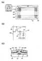
도 1(A)는 표시 장치의 구성을 나타낸 도면, 도 1(B)는 화소의 회로도, 도 1(C)은 화소에 설치되는 트랜지스터의 일례를 나타낸 단면도.
도 2는 표시 장치의 동작을 설명한 도면.
도 3은 표시 장치의 동작을 설명한 도면.
도 4는 표시 장치의 동작을 설명한 도면.
도 5(A)∼도 5(C)는 표시 장치의 화소에 설치되는 트랜지스터의 일례를 나타낸 단면도.
도 6은 관련된 표시 장치의 구성을 나타낸 도면.
도 7(A)∼도 7(D)는 트랜지스터를 설명한 도면.
도 8은 전자기기를 설명한 도면.
도 9는 트랜지스터의 특성을 나타낸 도면.
도 10은 트랜지스터의 특성 평가용 회로도.
도 11은 트랜지스터의 특성 평가용 타이밍 차트.
도 12는 트랜지스터의 특성을 나타낸 도면.
도 13은 트랜지스터의 특성을 나타낸 도면.
도 14는 트랜지스터의 특성을 나타낸 도면.1B is a circuit diagram of a pixel, and Fig. 1C is a cross-sectional view showing an example of a transistor provided in a pixel. Fig. 1A is a diagram showing the configuration of a display device. Fig.
2 is a view for explaining the operation of the display device;
3 is a view for explaining the operation of the display device;
4 is a view for explaining the operation of the display device;
5 (A) to 5 (C) are cross-sectional views showing an example of a transistor provided in a pixel of a display device.
6 is a diagram showing a configuration of a related display apparatus;
7A to 7D are views for explaining a transistor.
8 is a view for explaining an electronic apparatus;
9 is a diagram showing the characteristics of a transistor.
10 is a circuit diagram for evaluating characteristics of a transistor.
11 is a timing chart for evaluating characteristics of a transistor.
12 is a diagram showing the characteristics of a transistor.
13 is a diagram showing the characteristics of a transistor.
14 is a diagram showing the characteristics of a transistor.
이하에서는, 본 발명의 실시형태에 대하여 도면을 이용하여 상세하게 설명한다. 단, 본 발명은 이하의 설명에 한정되는 것은 아니고, 본 발명의 취지 및 그 범위로부터 벗어나지 않고 그 형태 및 상세한 사항을 다양하게 변경할 수 있다는 것은, 당업자라면 용이하게 이해할 수 있을 것이다. 따라서, 본 발명은 이하에 나타내는 실시형태의 기재 내용에 한정하여 해석되는 것은 아니다.Hereinafter, embodiments of the present invention will be described in detail with reference to the drawings. It should be understood, however, by those skilled in the art that the present invention is not limited to the following description, and that various changes in form and details may be made without departing from the spirit and scope of the present invention. Therefore, the present invention is not construed as being limited to the description of the embodiments described below.
(액티브 매트릭스형의 표시 장치의 일례에 대하여)(For an example of an active matrix type display device)
먼저, 액티브 매트릭스형의 표시 장치의 일례에 대하여 설명한다. 구체적으로는, 1 화면을 주사하는 주사 기간과, 이 주사 기간에 계속되고, 또한 이 주사 기간보다 긴 휴지 기간이 제공된 액티브 매트릭스형의 액정 표시 장치의 일례에 대하여 도 1∼도 6을 참조하여 설명한다. 또한, 이 주사 기간은 매트릭스 형상으로 배열된 복수의 화소 전부에 대하여, 데이터 신호의 입력이 1회 행해지는 기간이며, 이 휴지 기간은 매트릭스 형상으로 배열된 복수의 화소 전부에 대하여, 데이터 신호의 입력을 하지 않는 기간이다.First, an example of an active matrix type display device will be described. Specifically, an example of an active matrix type liquid crystal display device provided with a scanning period for scanning one screen and a rest period subsequent to the scanning period and longer than the scanning period is described with reference to Figs. 1 to 6 do. The scanning period is a period in which data signals are input once for all of a plurality of pixels arranged in a matrix, and the pause period is a period for inputting a data signal to all of a plurality of pixels arranged in a matrix .
도 1(A)은 액티브 매트릭스형의 표시 장치의 구성예를 나타낸 도면이다. 도 1(A)에 나타낸 표시 장치는, 화소부(101)와, 신호선 구동 회로(102)와, 주사선 구동 회로(103)와, 각각이 평행 또는 대략 평행으로 배열되고, 또한 신호선 구동 회로(102)에 의해 전위가 제어되는 복수의 신호선(104)과, 각각이 평행 또는 대략 평행으로 배열되고, 또한 주사선 구동 회로(103)에 의해 전위가 제어되는 복수의 주사선(105)을 가진다. 또한, 화소부(101)는 복수의 화소(107)를 가진다. 또한, 복수의 화소(107)는 매트릭스 형상으로 배열하고 있다. 또한, 복수의 신호선(104)의 각각은 매트릭스 형상으로 배열된 복수의 화소 중, 몇 개의 열에 배열된 복수의 화소에 전기적으로 접속되고, 복수의 주사선(105)의 각각은 매트릭스 형상으로 배열된 복수의 화소 중, 몇 개의 행에 배열된 복수의 화소에 전기적으로 접속된다. 또한, 신호선 구동 회로(102) 및 주사선 구동 회로(103)에는, 외부로부터 신호(데이터 신호(Data), 클록 신호(CK), 스타트 신호(SP) 등) 및 구동용 전원(고전원 전위(Vdd), 저전원 전위(Vss) 등)이 입력된다.Fig. 1 (A) is a diagram showing a configuration example of an active matrix type display device. The display device shown in Fig. 1A includes a
도 1(B)은 도 1(A)에 나타낸 표시 장치가 가지는 화소(107)의 회로도의 일례를 나타낸 도면이다. 도 1(B)에 나타낸 화소(107)는 게이트가 주사선(105)에 전기적으로 접속되고, 소스 및 드레인의 한쪽이 신호선(104)에 전기적으로 접속된 트랜지스터(111)와, 한쪽의 단자가 트랜지스터(111)의 소스 및 드레인의 다른 한쪽에 전기적으로 접속되고, 다른 한쪽의 단자가 공통 전위(Vcom)를 공급하는 배선(공통 전위선이라고도 함)에 전기적으로 접속된 용량 소자(112)와, 한쪽의 단자가 트랜지스터(111)의 소스 및 드레인의 다른 한쪽 및 용량 소자(112)의 한쪽의 단자에 전기적으로 접속되고, 다른 한쪽의 단자가 공통 전위선에 전기적으로 접속된 액정 소자(113)를 가진다. 또한, 트랜지스터(111)는 n 채널형의 트랜지스터이다. 또한, 트랜지스터(111)의 소스 및 드레인의 다른 한쪽, 용량 소자(112)의 한쪽의 단자, 및 액정 소자(113)의 한쪽의 단자가 전기적으로 접속하는 노드를 노드(A)라고 부르기로 한다.Fig. 1B is a diagram showing an example of a circuit diagram of the
도 1(C)은 도 1(B)에 나타낸 화소(107)에 설치된 트랜지스터(111)의 구체적인 구조의 일례를 나타낸 도면이다. 도 1(C)에 나타낸 트랜지스터(111)는 절연 표면을 가지는 기판(120) 위에 형성된 게이트층(121)과, 게이트층(121) 위에 형성된 게이트 절연층(122)과, 게이트 절연층(122) 위에 형성된 산화물 반도체층(123)과, 산화물 반도체층(123) 위에 형성된 소스층(124a) 및 드레인층(124b)을 가진다. 또한, 도 1(C)에 나타낸 트랜지스터(111)에서는, 트랜지스터(111)를 덮어, 산화물 반도체층(123)에 접하는 절연층(125)과, 절연층(125) 위에 형성된 보호 절연층(126)이 형성되어 있다.Fig. 1 (C) is a diagram showing an example of the specific structure of the
도 1(C)에 나타낸 트랜지스터(111)는 상기한 바와 같이, 반도체층으로서 산화물 반도체층(123)을 구비한다. 산화물 반도체층(123)에 이용하는 산화물 반도체로서는, 4원계 금속 산화물인 In-Sn-Ga-Zn-O계, 3원계 금속 산화물인 In-Ga-Zn-O계, In-Sn-Zn-O계, In-Al-Zn-O계, Sn-Ga-Zn-O계, Al-Ga-Zn-O계, Sn-Al-Zn-O계, 2원계 금속 산화물인 In-Zn-O계, In-Ga-O계, Sn-Zn-O계, Al-Zn-O계, Zn-Mg-O계, Sn-Mg-O계, In-Mg-O계, 또는 단원계 금속 산화물인 In-O계, Sn-O계, Zn-O계 등을 이용할 수 있다. 또한, 상기 산화물 반도체에 SiO2를 포함해도 좋다. 여기서, 예를 들면, In-Ga-Zn-O계 산화물 반도체란, 적어도 In과 Ga와 Zn을 포함하는 산화물이며, 그 조성비에 특별히 제한은 없다. 또한, In과 Ga와 Zn 이외의 원소를 포함해도 좋다.The
또한, 산화물 반도체층(123)은, 화학식 InMO3(ZnO)m(m>0)으로 표기되는 박막을 이용할 수 있다. 여기서, M은, Ga, Al, Mn 및 Co로부터 선택된 하나 또는 복수의 금속 원소를 나타낸다. 예를 들면 M으로서 Ga, Ga 및 Al, Ga 및 Mn, 또는 Ga 및 Co 등을 선택할 수 있다.As the
상술한 산화물 반도체는, 변동 요인이 되는 수소, 수분, 수산기 또는 수소화물(수소 화합물이라고도 함) 등의 불순물을 의도적으로 배제함으로써 고순도화하여, 전기적으로 I형(진성)화된 산화물 반도체이다. 이것에 의해, 이 산화물 반도체를 반도체층으로서 이용한 트랜지스터의 전기적 특성 변동을 억제할 수 있다.The above-described oxide semiconductor is an oxide semiconductor which is highly purity and intrinsically I-type (intrinsic) by intentionally eliminating impurities such as hydrogen, moisture, hydroxyl groups or hydrides (also referred to as hydrogen compounds) This makes it possible to suppress variations in the electrical characteristics of the transistor using the oxide semiconductor as the semiconductor layer.
따라서 산화물 반도체 중의 수소는 적으면 적을수록 좋다. 또한, 고순도화된 산화물 반도체층 중에는 수소나 산소 결손 등에 유래하는 캐리어가 매우 적고(제로에 가까움), 캐리어 밀도는 1×10¹²/cm3 미만, 바람직하게는 1×10¹¹/cm3 미만이다. 즉, 산화물 반도체층의 수소나 산소 결손 등에 유래하는 캐리어 밀도를 한없이 제로에 가깝게 한다. 산화물 반도체층 중에 수소나 산소 결손 등에 유래하는 캐리어가 매우 적기 때문에, 트랜지스터의 오프 전류를 줄일 수 있다. 오프 전류는 적으면 적을수록 바람직하다. 상기 산화물 반도체를 반도체층으로서 이용한 트랜지스터는, 채널 폭(w) 1μm당의 전류값이 100 zA(젭토암페어) 이하, 바람직하게는 10 zA 이하, 더욱 바람직하게는 1 zA 이하이다. 또한, pn 접합이 없고, 핫 캐리어 열화가 없기 때문에, 트랜지스터의 전기적 특성이 이들 요인의 영향을 받지 않는다.Therefore, the smaller the number of hydrogen in the oxide semiconductor, the better. In the high purity oxide semiconductor layer, the carrier derived from hydrogen or oxygen defects is very small (close to zero) and the carrier density is less than 1 x 10¹² / cm3 , preferably less than 1 x 10¹¹ / cm3 . That is, the carrier density derived from hydrogen, oxygen deficiency, etc. of the oxide semiconductor layer is made almost zero. Since the carriers derived from hydrogen, oxygen defects and the like are very few in the oxide semiconductor layer, the off current of the transistor can be reduced. The smaller the off current, the better. In the transistor using the oxide semiconductor as the semiconductor layer, the current value per 1 μm channel width (w) is 100 zA (loft amperes) or less, preferably 10 zA or less, more preferably 1 zA or less. Further, since there is no pn junction and there is no hot carrier deterioration, the electrical characteristics of the transistor are not influenced by these factors.
이와 같이 산화물 반도체층에 포함되는 수소를 철저하게 제거함으로써 고순도화된 산화물 반도체를 채널 형성 영역에 이용한 트랜지스터는 오프 전류를 매우 작게 할 수 있다. 즉, 트랜지스터의 비도통 상태에서, 산화물 반도체층은 절연체로 간주할 수 있어, 회로 설계를 행할 수 있다. 한편, 산화물 반도체층은 트랜지스터의 도통 상태에서, 비정질 실리콘으로 형성되는 반도체층보다 높은 전류 공급 능력을 예상할 수 있다.In this way, the off current can be very small in the transistor using the highly purified oxide semiconductor as the channel forming region by thoroughly removing the hydrogen contained in the oxide semiconductor layer. That is, in the non-conduction state of the transistor, the oxide semiconductor layer can be regarded as an insulator, and circuit design can be performed. On the other hand, in the conduction state of the transistor, the oxide semiconductor layer can be expected to have higher current supply capability than the semiconductor layer formed of amorphous silicon.
절연 표면을 가지는 기판(120)으로서, 사용할 수 있는 기판에 큰 제한은 없다. 예를 들면, 바륨 붕규산 유리나 알루미노 붕규산 유리 등의 유리 기판을 이용할 수 있다.As the
트랜지스터(111)에 있어서, 베이스막이 되는 절연막을 기판(120)과 게이트층(121)의 사이에 형성해도 좋다. 베이스막은 기판으로부터의 불순물 원소의 확산을 방지하는 기능이 있고, 질화 실리콘막, 산화 실리콘막, 질화 산화 실리콘막, 또는 산화 질화 실리콘막으로부터 선택된 하나 또는 복수의 막에 의한 적층 구조에 의해 형성할 수 있다.In the
게이트층(121)의 재료는, 몰리브덴, 티탄, 크롬, 탄탈, 텅스텐, 알루미늄, 구리, 네오디뮴, 스칸듐 등의 금속 재료 또는 이것들을 주성분으로 하는 합금 재료를 이용하여, 단층으로 또는 적층하여 형성할 수 있다.The material of the
게이트 절연층(122)은 플라즈마 CVD법 또는 스퍼터링법 등을 이용하여, 산화 실리콘층, 질화 실리콘층, 산화 질화 실리콘층, 질화 산화 실리콘층, 산화 알루미늄층, 질화 알루미늄층, 산화 질화 알루미늄층, 질화 산화 알루미늄층, 또는 산화 하프늄층을 단층으로 또는 적층하여 형성할 수 있다. 예를 들면, 제 1 게이트 절연층으로서 플라즈마 CVD법에 의해 막두께 50 nm 이상 200 nm 이하의 질화 실리콘층(SiNy(y>0))를 형성하고, 제 1 게이트 절연층 위에 제 2 게이트 절연층으로서, 막두께 5 nm 이상 300 nm 이하의 산화 실리콘층(SiOx(x>0))을 적층할 수 있다.The
소스층(124a), 드레인층(124b)에 이용하는 도전막으로서는, 예를 들면, Al, Cr, Cu, Ta, Ti, Mo, W로부터 선택된 원소, 또는 상술한 원소를 성분으로 하는 합금이나, 상술한 원소를 조합한 합금막 등을 이용할 수 있다. 또한, Al, Cu 등의 금속층의 하측 또는 상측의 한쪽 또는 쌍방에 Ti, Mo, W 등의 고융점 금속층을 적층시킨 구성으로 해도 좋다. 또한, Al막에 생기는 힐록이나 위스커의 발생을 방지하는 원소(Si, Nd, Sc 등)가 첨가되어 있는 Al 재료를 이용함으로써 내열성을 향상시키는 것이 가능하게 된다.As the conductive film used for the
또한, 소스층(124a), 드레인층(124b)(이것들과 같은 층으로 형성되는 배선층을 포함함)이 되는 도전막으로서는 도전성의 금속 산화물로 형성해도 좋다. 도전성의 금속 산화물로서는 산화 인듐(In2O3), 산화 주석(SnO2), 산화 아연(ZnO), 산화 인듐 산화 주석 합금(In2O3―SnO2, ITO라고 약기함), 산화 인듐 산화 아연 합금(In2O3―ZnO) 또는 이들의 금속 산화물 재료에 산화 실리콘을 포함시킨 것을 이용할 수 있다.In addition, the conductive film to be the
절연층(125)은 대표적으로는 산화 실리콘막, 산화 질화 실리콘막, 산화 알루미늄막, 또는 산화 질화 알루미늄막 등의 무기 절연막을 이용할 수 있다.As the insulating
보호 절연층(126)은 질화 실리콘막, 질화 알루미늄막, 질화 산화 실리콘막, 질화 산화 알루미늄막 등의 무기 절연막을 이용할 수 있다.As the protective insulating
또한, 보호 절연층(126) 위에 트랜지스터에 기인한 표면 요철을 저감하기 위해 평탄화 절연막을 형성해도 좋다. 평탄화 절연막으로서는, 폴리이미드, 아크릴, 벤조시클로부텐, 등의 유기 재료를 이용할 수 있다. 또한, 상기 유기 재료 외에, 저유전율 재료(low-k 재료) 등을 이용할 수 있다. 또한, 이들 재료로 형성되는 절연막을 복수 적층시킴으로써, 평탄화 절연막을 형성해도 좋다.In addition, a planarization insulating film may be formed on the protective insulating
(트랜지스터의 오프 전류에 대하여)(With respect to the off current of the transistor)
다음에, 고순도화된 산화물 반도체층을 구비하는 트랜지스터의 오프 전류를 구한 결과에 대하여 설명한다.Next, a description will be given of the result of determining the off current of the transistor including the oxide semiconductor layer of high purity.
먼저, 고순도화된 산화물 반도체층을 구비하는 트랜지스터의 오프 전류가 충분히 작은 것을 고려하여, 채널 폭(W)이 1 m로 충분히 큰 트랜지스터를 준비하여 오프 전류의 측정을 행하였다. 채널 폭(W)이 1 m인 트랜지스터의 오프 전류를 측정한 결과를 도 9에 나타낸다. 도 9에서, 횡축은 게이트 전압(VG), 종축은 드레인 전류(ID)이다. 드레인 전압(VD)이 +1 V 또는 +10 V인 경우, 게이트 전압(VG)이 ―5 V에서 ―20 V의 범위에서, 트랜지스터의 오프 전류는, 검출 한계인 1×10-12 A 이하인 것을 알 수 있었다. 또한, 트랜지스터의 오프 전류(여기에서는, 단위 채널 폭(1μm)당의 값)은 1 aA/μm(1×10-18 A/μm) 이하가 되는 것을 알 수 있었다.First, in consideration of the fact that the off current of the transistor including the oxide semiconductor layer of high purity was sufficiently small, a transistor having a sufficiently large channel width W of 1 m was prepared and the off current was measured. Fig. 9 shows the results of measuring the off current of the transistor having the channel width W of 1 m. In Fig. 9, the horizontal axis is the gate voltage (VG) and the vertical axis is the drain current (ID). It can be seen that when the drain voltage VD is +1 V or +10 V, the off current of the transistor is 1 × 10-12 A or less, which is the detection limit, when the gate voltage VG is in the range of -5 V to -20 V there was. It was also found that the off current of the transistor (here, the value per unit channel width (1 μm)) was 1 aA / μm (1 × 10-18 A / μm) or less.
다음에, 고순도화된 산화물 반도체층을 구비하는 트랜지스터의 오프 전류를 더욱 정확하게 구한 결과에 대하여 설명한다. 상술한 바와 같이, 고순도화된 산화물 반도체층을 구비하는 트랜지스터의 오프 전류는, 측정기의 검출 한계인 1×10-12 A 이하인 것을 알 수 있었다. 따라서, 특성 평가용 소자를 제작하여, 보다 정확한 오프 전류의 값(상기 측정에서의 측정기의 검출 한계 이하의 값)을 구한 결과에 대하여 설명한다.Next, a description will be given of the result of more accurately determining the off current of the transistor including the oxide semiconductor layer of high purity. As described above, it was found that the off current of the transistor including the oxide semiconductor layer of high purity was not more than 1 × 10-12 A, which is the detection limit of the measuring device. Therefore, a description will be made of a result of obtaining a more accurate off current value (a value below the detection limit of the measuring instrument in the measurement) by fabricating a characteristic evaluation element.
먼저, 전류 측정 방법에 이용한 특성 평가용 소자에 대하여, 도 10을 참조하여 설명한다.First, a characteristic evaluation element used in a current measuring method will be described with reference to FIG.
도 10에 나타낸 특성 평가용 소자는 측정계(800)가 3개 병렬로 접속되어 있다. 측정계(800)는, 용량 소자(802), 트랜지스터(804), 트랜지스터(805), 트랜지스터(806), 트랜지스터(808)를 가진다. 트랜지스터(804), 트랜지스터(808)에는, 고순도화된 산화물 반도체층을 구비하는 트랜지스터를 적용했다.In the characteristic evaluation device shown in Fig. 10, three
측정계(800)에 있어서, 트랜지스터(804)의 소스 단자 및 드레인 단자의 한쪽과 용량 소자(802)의 단자의 한쪽과, 트랜지스터(805)의 소스 단자 및 드레인 단자의 한쪽은, 전원(V2를 부여하는 전원)에 접속되어 있다. 또한, 트랜지스터(804)의 소스 단자 및 드레인 단자의 다른 한쪽과, 트랜지스터(808)의 소스 단자 및 드레인 단자의 한쪽과, 용량 소자(802)의 단자의 다른 한쪽과, 트랜지스터(805)의 게이트 단자는 접속되어 있다. 또한, 트랜지스터(808)의 소스 단자 및 드레인 단자의 한쪽과, 트랜지스터(806)의 소스 단자 및 드레인 단자의 한쪽과, 트랜지스터(806)의 게이트 단자는 전원(V1을 부여하는 전원)에 접속되어 있다. 또한, 트랜지스터(805)의 소스 단자 및 드레인 단자의 다른 한쪽과, 트랜지스터(806)의 소스 단자 및 드레인 단자의 다른 한쪽은, 출력 단자에 접속되어 있다.One of the source terminal and the drain terminal of the
또한, 트랜지스터(804)의 게이트 단자에는 트랜지스터(804)의 온 상태와 오프 상태를 제어하는 전위(Vext_b2)가 공급되고, 트랜지스터(808)의 게이트 단자에는 트랜지스터(808)의 온 상태와 오프 상태를 제어하는 전위(Vext_b1)가 공급된다. 또한, 출력 단자로부터는 전위(Vout)가 출력된다.A potential Vext_b2 for controlling the on and off states of the
다음에, 상기의 특성 평가용 소자를 이용한 전류 측정 방법에 대하여 설명한다.Next, a current measurement method using the above-described characteristic evaluation element will be described.
먼저, 오프 전류를 측정하기 위해 전위차를 부여하는 초기화 기간의 대략에 대하여 설명한다. 초기화 기간에는, 트랜지스터(808)의 게이트 단자에 트랜지스터(808)를 온 상태로 하는 전위(Vext_b1)를 입력하고, 트랜지스터(804)의 소스 단자 및 드레인 단자의 다른 한쪽과 접속되는 노드(즉, 트랜지스터(808)의 소스 단자 및 드레인 단자의 한쪽, 용량 소자(802)의 단자의 다른 한쪽, 및 트랜지스터(805)의 게이트 단자에 접속되는 노드)인 노드(A)에 전위(V1)를 부여한다. 여기서, 전위(V1)는 예를 들면 고전위로 한다. 또한, 트랜지스터(804)는 오프 상태로 해둔다.First, a description will be given of the approximate initial period in which a potential difference is given to measure the off current. A potential Vext_b1 for turning on the
그 후, 트랜지스터(808)의 게이트 단자에, 트랜지스터(808)를 오프 상태로 하는 전위(Vext_b1)를 입력하고, 트랜지스터(808)를 오프 상태로 한다. 트랜지스터(808)를 오프 상태로 한 후에, 전위(V1)를 저전위로 한다. 여기에서도, 트랜지스터(804)는 오프 상태로 해둔다. 또한, 전위(V2)는 전위(V1)와 같은 전위로 한다. 이상에 의해, 초기화 기간이 종료된다. 초기화 기간이 종료된 상태에서는, 노드(A)와 트랜지스터(804)의 소스 단자 및 드레인 단자의 한쪽과의 사이에 전위차가 생기고, 또한, 노드(A)와 트랜지스터(808)의 소스 단자 및 드레인 단자의 다른 한쪽과의 사이에 전위차가 생기게 되기 때문에, 트랜지스터(804) 및 트랜지스터(808)에는 전하가 약간 흐른다. 즉, 오프 전류가 발생한다.Thereafter, a potential Vext_b1 for turning off the
다음에, 오프 전류의 측정 기간의 대략에 대하여 설명한다. 측정 기간에는, 트랜지스터(804)의 소스 단자 및 드레인 단자의 한쪽의 단자의 전위(즉 V2), 및, 트랜지스터(808)의 소스 단자 및 드레인 단자의 다른 한쪽의 단자의 전위(즉 V1)는 저전위로 고정해둔다. 한편, 측정 기간 중에, 상기 노드(A)의 전위는 고정하지 않는다(플로팅 상태로 함). 이것에 의해, 트랜지스터(804), 트랜지스터(808)에 전하가 흘러, 시간의 경과와 함께 노드(A)에 보유되는 전하량이 변동한다. 그리고 노드(A)에 보유되는 전하량의 변동에 따라, 노드(A)의 전위가 변동한다. 즉, 출력 단자의 출력 전위(Vout)도 변동한다.Next, the measurement period of the off current will be roughly described. During the measurement period, the potential (i.e., V2) of one of the source terminal and the drain terminal of the
상기 전위차를 부여하는 초기화 기간, 및, 그 후의 측정 기간에서의 각 전위의 관계의 상세한 사항(타이밍 차트)을 도 11에 나타낸다.Fig. 11 shows details (timing chart) of the relationship between the potentials in the initialization period for giving the potential difference and the subsequent measurement period.
초기화 기간에 있어서, 먼저, 전위(Vext_b2)를 트랜지스터(804)가 온 상태가 되는 전위(고전위)로 한다. 이것에 의해, 노드(A)의 전위는 V2 즉 저전위(VSS)가 된다. 또한, 노드(A)에 저전위(VSS)를 부여하는 것은 필수는 아니다. 그 후, 전위(Vext_b2)를 트랜지스터(804)가 오프 상태가 되는 전위(저전위)로 하여, 트랜지스터(804)를 오프 상태로 한다. 그리고 다음에, 전위(Vext_b1)를 트랜지스터(808)가 온 상태가 되는 전위(고전위)로 한다. 이것에 의해, 노드(A)의 전위는 V1, 즉 고전위(VDD)가 된다. 그 후, Vext_b1을 트랜지스터(808)가 오프 상태가 되는 전위로 한다. 이것에 의해, 노드(A)가 플로팅 상태가 되어, 초기화 기간이 종료된다.In the initialization period, first, the potential Vext_b2 is set to the potential (high potential) at which the
그 후의 측정 기간에서는, 전위(V1) 및 전위(V2)를 노드(A)에 전하가 흘러들어가거나, 또는 노드(A)로부터 전하가 흘러나오는 전위로 한다. 여기에서는, 전위(V1) 및 전위(V2)를 저전위(VSS)로 한다. 단, 출력 전위(Vout)를 측정하는 타이밍에서는, 출력 회로를 동작시킬 필요가 생기기 때문에, 일시적으로 V1을 고전위(VDD)로 하는 일이 있다. 또한, V1을 고전위(VDD)로 하는 기간은 측정에 영향을 주지 않을 정도의 단기간으로 한다.In the subsequent measurement period, the potential V1 and the potential V2 are set to the potential at which electric charge flows into the node A, or electric charge flows from the node A. [ Here, the potential V1 and the potential V2 are set to the low potential VSS. However, since it is necessary to operate the output circuit at the timing of measuring the output potential Vout, V1 may be temporarily set to the high potential (VDD). The period for setting V1 to the high potential (VDD) is set to a short period that does not affect the measurement.
위에서 설명한 바와 같이 하여 전위차를 부여하여, 측정 기간이 개시되면, 시간의 경과와 함께 노드(A)에 보유되는 전하량이 변동하고, 이것에 따라 노드(A)의 전위가 변동한다. 이것은, 트랜지스터(805)의 게이트 단자의 전위가 변동하는 것을 의미하기 때문에, 시간의 경과와 함께, 출력 단자의 출력 전위(Vout)의 전위도 변화하게 된다.As described above, a potential difference is applied. When the measurement period starts, the amount of charge held in the node A changes with the elapse of time, and the potential of the node A fluctuates accordingly. This means that the potential of the gate terminal of the
얻어진 출력 전위(Vout)로부터, 오프 전류를 산출하는 방법에 대하여, 이하에 설명한다.A method of calculating the off current from the obtained output potential Vout will be described below.
오프 전류의 산출에 앞서, 노드(A)의 전위(VA)와 출력 전위(Vout)와의 관계를 구해둔다. 이것에 의해, 출력 전위(Vout)로부터 노드(A)의 전위(VA)를 구할 수 있다. 상기 관계로부터, 노드(A)의 전위(VA)는 출력 전위(Vout)의 함수로서 다음식과 같이 나타낼 수 있다.Prior to the calculation of the off current, the relationship between the potential VA of the node A and the output potential Vout is obtained. Thus, the potential VA of the node A can be obtained from the output potential Vout. From the above relationship, the potential VA of the node A can be expressed as a function of the output potential Vout as follows.
[수학식 1][Equation 1]

또한, 노드(A)의 전하(QA)는, 노드(A)의 전위(VA), 노드(A)에 접속되는 용량(CA), 정수(const)를 이용하여, 다음식과 같이 나타내어진다. 여기서, 노드(A)에 접속되는 용량(CA)은 용량 소자(802)의 용량과 다른 용량의 합이다.The charge QA of the node A is expressed by the following equation using the potential VA of the node A, the capacitance CA connected to the node A, and the constant const. Here, the capacitance CA connected to the node A is the sum of the capacitance of the
[수학식 2]&Quot; (2) "

노드(A)의 전류(IA)는, 노드(A)에 흘러들어가는 전하(또는 노드(A)로부터 흘러나오는 전하)의 시간 미분이기 때문에, 노드(A)의 전류(IA)는 다음식과 같이 나타내어진다.Since the current IA of the node A is a time derivative of the charge flowing into the node A (or the charge flowing out of the node A), the current IA of the node A is expressed by the following equation Loses.
[수학식 3]&Quot; (3) "

이와 같이, 노드(A)에 접속되는 용량(CA)과, 출력 단자의 출력 전위(Vout)로부터, 노드(A)의 전류(IA)를 구할 수 있다.As described above, the current IA of the node A can be obtained from the capacitance CA connected to the node A and the output potential Vout of the output terminal.
이상에 나타낸 방법에 의해, 오프 상태에서 트랜지스터의 소스와 드레인 사이를 흐르는 오프 전류를 측정할 수 있다.With the above-described method, it is possible to measure the off current flowing between the source and the drain of the transistor in the off state.
여기에서는, 채널 길이 L = 10μm, 채널 폭(W) = 50μm의, 고순도화한 산화물 반도체층을 구비하는 트랜지스터(804), 고순도화된 산화물 반도체를 구비하는 트랜지스터(808)를 제작했다. 또한, 병렬된 각 측정계(800)에 있어서, 용량 소자(802)의 각 용량값을 100 fF, 1 pF, 3 pF로 했다.Here, the
또한, 상술한 측정에서는, VDD = 5 V, VSS = 0 V로 했다. 또한, 측정 기간에서는, 전위(V1)를 원칙으로 하여 VSS로 하고, 10∼300 sec마다 100 msec의 기간만 VDD로 하여 Vout를 측정했다. 또한, 소자에 흐르는 전류(I)의 산출에 이용되는 Δt는 약 30000 sec로 했다.In the above-described measurement, VDD = 5 V and VSS = 0 V were set. In the measurement period, the potential V1 was set to VSS as a rule, and Vout was measured at a VDD of only 100 msec every 10 to 300 sec. In addition,? T used for calculation of the current (I) flowing in the device was about 30000 sec.
도 12에 상기 전류 측정에 관한 경과 시간(Time)과 출력 전위(Vout)와의 관계를 나타낸다. 도 12로부터, 시간의 경과에 따라, 전위가 변화하는 양태를 확인할 수 있다.FIG. 12 shows the relationship between the elapsed time (Time) and the output potential (Vout) concerning the current measurement. From Fig. 12, it can be seen that the electric potential changes in accordance with the lapse of time.
도 13에는, 상기 전류 측정에 의해 산출된 실온(25℃)에서의 오프 전류를 나타낸다. 또한, 도 13은 트랜지스터(804) 또는 트랜지스터(808)의 소스―드레인 전압(V)과 오프 전류(I)와의 관계를 나타내는 것이다. 도 13으로부터, 소스―드레인 전압이 4 V의 조건에서, 오프 전류는 약 40 zA/μm인 것을 알 수 있었다. 또한, 소스―드레인 전압이 3.1 V의 조건에서, 오프 전류는 10 zA/μm 이하인 것을 알 수 있었다. 또한, 1 zA는 10-21 A를 나타낸다.13 shows the off current at room temperature (25 DEG C) calculated by the current measurement. 13 shows the relationship between the source-drain voltage V and the off-current I of the
또한, 상기 전류 측정에 의해 산출된 85℃의 온도 환경 하에서의 오프 전류에 대하여 도 14에 나타낸다. 도 14는 85℃의 온도 환경 하에서의 소스―드레인 전압(V)와 오프 전류(I)와의 관계를 나타낸 것이다. 도 14로부터, 소스―드레인 전압이 3.1 V의 조건에서, 오프 전류는 100 zA/μm 이하인 것을 알 수 있었다.The off current in the temperature environment of 85 캜 calculated by the current measurement is shown in Fig. 14 shows the relationship between the source-drain voltage (V) and the off-current (I) under a temperature environment of 85 캜. 14, it was found that the off current was 100 zA / μm or less under the condition that the source-drain voltage was 3.1 V.
이상에 의해, 고순도화된 산화물 반도체층을 구비하는 트랜지스터에서는 오프 전류가 충분히 작아지는 것이 확인되었다.As described above, it was confirmed that the off current was sufficiently reduced in the transistor including the oxide semiconductor layer of high purity.
(액티브 매트릭스형의 표시 장치의 동작의 일례에 대하여)(Regarding Example of Operation of Display Device of Active Matrix Type)
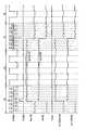
다음에, 상술한 표시 장치의 동작의 일례에 대하여, 도 2를 참조하여 설명한다. 또한, 도 2에는, 도 1(B)에 나타낸 신호선(104)의 전위(V(104)), 주사선(105)의 전위(V(105)), 트랜지스터(111)가 산화물 반도체층을 구비하는 트랜지스터인 경우의 노드(A)의 전위(A(OS)), 공통 전위(Vcom), 및 트랜지스터(111)가 산화물 반도체층을 구비하는 트랜지스터인 경우의 액정 소자(113)에 인가되는 전압(V(113)(OS))을 모식적으로 나타낸다. 또한, 도 2에서는, 트랜지스터(111)가 아몰퍼스(amorphous) 실리콘층을 구비하는 트랜지스터인 경우의 노드(A)의 전위(A(a-Si)), 및 트랜지스터(111)가 아몰퍼스 실리콘층을 구비하는 트랜지스터인 경우의 액정 소자(113)에 인가되는 전압(V(113)(a-Si))을, 비교를 위해, 모식적으로 나타내고 있다.Next, an example of the operation of the above-described display apparatus will be described with reference to Fig. 2 shows an example in which the potential V (104) of the
신호선(104)에는, 주사 기간(T1)에 데이터 신호가 공급되고, 휴지 기간(T2)에 교류의 구동 신호가 공급된다. 또한, 이 데이터 신호는 1 수평 주사 기간(t:1 게이트 선택 기간이라고도 함)마다 극성이 반전하는 신호이다. 즉, 본 명세서에 개시되는 표시 장치는, 게이트 라인 반전 구동을 행하는 표시 장치이다. 또한, 이 데이터 신호는 아날로그 신호이다. 또한, 이 구동 신호는 적어도 1 수평 주사 기간보다 긴 기간마다 극성이 반전하는 교류의 신호이다. 또한, 이 구동 신호는 2치(値)의 신호이다. 또한, 이 구동 신호의 전압의 변동을, 데이터 신호의 전압 변동 범위 내로 할 수 있다.A data signal is supplied to the
주사선(105)에는, 주사 기간(T1)에 포함되는 특정의 1 수평 주사 기간에 하이 레벨의 전위(선택 신호)가 공급되고, 그 이외의 기간에는 로 레벨의 전위(비선택 신호)가 공급된다. 즉, 화소(107)가 가지는 트랜지스터(111)는 이 1 수평 주사 기간에 있어서 온 상태가 되고, 그 이외의 기간에는 오프 상태가 된다.A high level potential (selection signal) is supplied to the
노드(A)에는, 1 수평 주사 기간에 있어서 트랜지스터(111)를 통하여 신호선(104)으로부터 데이터 신호가 공급되고, 그 이외의 기간에는 신호가 공급되지 않는다. 즉, 이 1 수평 주사 기간 이외의 기간에는, 노드(A)는 부유 상태가 된다. 따라서, 이 1 수평 주사 기간 이외의 기간에 있어서, 노드(A)의 전위는 신호선(104)과 노드(A)의 용량 결합에 의해 변동한다. 또한, 용량 결합에 기인한 노드(A)의 전위의 변동은 트랜지스터(111)가 아몰퍼스 실리콘층을 구비하는 트랜지스터인지, 산화물 반도체층을 구비하는 트랜지스터인지에 따라 크게 변화되는 일은 없다.The node A is supplied with the data signal from the
그러나, 트랜지스터(111)가 아몰퍼스 실리콘을 구비하는 트랜지스터인 경우와, 산화물 반도체를 구비하는 트랜지스터인 경우에는, 휴지 기간에서의 노드(A)의 전위의 변동량이 다르다. 구체적으로는, 휴지 기간(T2)에서의 노드(A)의 전위의 변동량이, 산화물 반도체층을 구비하는 트랜지스터가 아몰퍼스 실리콘층을 구비하는 트랜지스터보다 작아진다(ΔV(a-Si)>ΔV(OS)가 됨). 이것은 산화물 반도체층을 구비하는 트랜지스터가 아몰퍼스 실리콘층을 구비하는 트랜지스터보다 오프 전류가 작은 것에 기인한다.However, when the
또한, 여기에서는, 공통 전위(Vcom)로서 고정 전위를 적용하고 있다. 이 고정 전위로서는, 접지 전위 또는 0 V 등을 적용할 수 있다.In addition, here, a fixed potential is applied as the common potential Vcom. As this fixed potential, a ground potential or 0 V or the like can be applied.
액정 소자(113)에는, 노드(A)의 전위와 공통 전위(Vcom)의 전위차분의 전압이 인가된다. 따라서, 액정 소자(113)에 인가되는 전압의 변화는 노드(A)의 전위의 변화와 같다.A voltage of a potential difference between the potential of the node A and the common potential Vcom is applied to the
화소(107)에서의 표시는 액정 소자(113)에 인가되는 전압에 의해 정해진다. 상술한 표시 장치에서, 이 전압은 신호선(104)과의 용량 결합 및 트랜지스터(111)에 생기는 오프 전류 등에 따라 변동한다. 따라서, 화소(107)에서의 실제의 표시는, 1 수평 주사 기간에서 화소(107)에 입력되는 데이터 신호에 기초하여 형성되는 표시와는 엄밀하게는 다르다. 구체예를 이하에 설명한다. 만일, 주사 기간에서, 화소(107)에 대하여 1초간에 60회(약 16.7 ms에 1회) 데이터 신호가 입력된다고 한다. 이 경우, 1 수평 주사 기간은 16.7 ms보다 월등하게 짧다. 여기에서는, 이 1 수평 주사 기간은 편의상 16.7μs로 한다(예를 들면, 표시 장치에서 매트릭스 형상으로 배열된 복수의 화소의 행수가 1000행이라고 하면, 이 1 수평 주사 기간은 16.7μs 정도가 된다). 이때, 신호선(104)에는, 화소(107)와 동렬(同列)에 형성된 화소에 대한 데이터 신호의 공급이 이 1 수평 주사 기간 이외의 기간에도 행해지기 때문에, 신호선(104)의 전위는 이 1 수평 주사 기간 이외의 기간에서도 변동한다. 따라서, 노드(A)의 전위도 신호선(104)과의 용량 결합에 의해 변동하고, 화소(107)에서의 16.7 ms 동안의 실질적인 표시는 이 1 수평 주사 기간(16.7μs)에 신호선(104)으로부터 공급되는 데이터 신호에 기초한 표시와는 엄밀하게는 다르다.The display on the
또한, 본 명세서에 개시되는 표시 장치는 휴지 기간을 가진다. 만일, 휴지 기간에 신호선(104)의 전위가 고정 전위가 되거나 또는 부유 상태가 되는 경우, 액정 소자(113)에 인가되는 전압의 변동에 대하여, 상술한 용량 결합에 의한 기여가 없어진다. 이 경우, 주사 기간에서의 화소(107)의 표시와, 휴지 기간에서의 화소(107)의 표시가 다르게 된다. 이것에 대하여, 본 명세서에 개시되는 표시 장치는, 휴지 기간에 있어서, 신호선(104)에 대하여 교류의 구동 신호를 공급하고 있다. 따라서, 휴지 기간에도, 주사 기간과 동일한 정도의 용량 결합에 의한 기여를, 액정 소자(113)에 인가되는 전압의 변동에 대하여 부여할 수 있다. 이것에 의해, 휴지 기간에서의 화소(107)의 표시를, 주사 기간에서의 표시와 마찬가지로 할 수 있다.Further, the display device disclosed in this specification has a rest period. If the potential of the
또한, 본 명세서에 개시되는 표시 장치는, 화소(107)에 설치된 트랜지스터(111)로서 산화물 반도체층을 구비하는 트랜지스터를 적용하고 있다. 이것에 의해, 액정 소자(113)에 인가되는 전압에 대한, 트랜지스터(111)의 오프 전류의 기여를 저감할 수 있다. 이것에 의해, 화소(107)에서의 신호의 보유 기간을 장기화할 수 있다. 즉, 휴지 기간을 장기화할 수 있다. 또한, 휴지 기간에 있어서, 액정 소자(113)에 인가되는 전압의 진폭을 저감하는 것이 가능하게 된다. 이것에 의해, 화소(107)에서의 표시의 플리커를 저감할 수 있다. 특히, 이 효과는, 신호선(104)에 공급되는 교류의 구동 신호의 주파수가 저감된 경우에 크다.In the display device disclosed in this specification, a transistor including an oxide semiconductor layer is used as the
이상과 같이, 본 명세서에 개시되는 표시 장치는, 산화물 반도체를 구비하는 트랜지스터를 트랜지스터(111)로서 적용함으로써, 휴지 기간이 장기화된 경우, 또는 휴지 기간에 신호선(104)에 공급되는 교류의 구동 신호의 주파수가 저감된 경우에도 표시 품질을 보유할 수 있는 표시 장치이다. 즉, 본 명세서에 개시되는 표시 장치는, 소비 전력의 저감 및 표시 품질의 저하의 억제가 가능한 표시 장치이다.As described above, the display device disclosed in this specification can be applied to a case where the
(액티브 매트릭스형의 표시 장치의 변형예에 대하여)(Regarding Modifications of the Active Matrix Display Device)
상술한 표시 장치는 본 발명의 일 양태이며, 이 표시 장치와 다른 점을 가지는 표시 장치도 본 발명에는 포함된다.The above-described display device is an aspect of the present invention, and a display device having a difference from this display device is also included in the present invention.
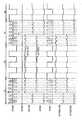
예를 들면, 상술한 표시 장치에서는, 공통 전위선에 고정 전위가 공급되는 구성에 대하여 나타냈지만, 주사 기간에 있어서, 공통 전위선에 교류의 구동 신호(제 1 공통 전위선용 구동 신호)가 공급되는 구성(소위, 코먼 반전 구동)으로 하는 것도 가능하다(도 3 참b 조). 이것에 의해, 데이터 신호의 전압 진폭을 반감하는 것이 가능하게 된다. 이 경우, 공통 전위선의 전위는 주사 기간에 데이터 신호와 역의 극성을 가지는 2치의 신호가 되어, 휴지 기간에 있어서 고정 전위를 가지는 신호가 된다.For example, in the above-described display device, the configuration in which the fixed potential is supplied to the common potential line is shown, but in the scanning period, the alternating drive signal (first common potential line drive signal) is supplied to the common potential line (So-called common inversion drive) (see Fig. 3b). This makes it possible to halve the voltage amplitude of the data signal. In this case, the potential of the common potential line becomes a binary signal having a polarity opposite to that of the data signal in the scanning period, and becomes a signal having a fixed potential in the rest period.
또한, 휴지 기간에서도, 공통 전위선에 교류의 구동 신호(제 2 공통 전위선용 구동 신호)를 공급하는 것도 가능하다(도 4 참조). 이 경우, 공통 전위선의 전위는, 주사 기간에 있어서 데이터 신호와 역의 극성을 가지는 2치의 신호(제 1 공통 전위선용 구동 신호)가 되어, 휴지 기간에 있어서 신호선(104)에 공급되는 교류의 구동 신호와 같은 극성을 가지는 2치의 신호(제 2 공통 전위선용 구동 신호)가 된다. 또한, 휴지 기간에 있어서, 공통 전위선에 공급되는 교류의 구동 신호(제 2 공통 전위선용 구동 신호)의 전압의 변동을, 주사 기간에 있어서, 공통 전위선에 공급되는 교류의 구동 신호(제 1 공통 전위선용 구동 신호)의 전압 변동 범위 내로 할 수 있다. 또한, 휴지 기간에 있어서, 공통 전위선에 공급되는 교류의 구동 신호(제 2 공통 전위선용 구동 신호)를, 휴지 기간에 있어서 신호선(104)에 공급되는 교류의 구동 신호와 동일한 신호로 하는 것도 가능하다.It is also possible to supply an AC drive signal (drive signal for the second common potential line) to the common potential line even in the rest period (see Fig. 4). In this case, the potential of the common potential line becomes a binary signal (driving signal for the first common potential line) having a polarity opposite to that of the data signal in the scanning period, and the driving of the AC supplied to the
또한, 상술한 표시 장치에서는, 휴지 기간에 신호선(104)에 공급되는 교류의 구동 신호가 2치의 신호인 구성에 대하여 나타냈지만, 이 구동 신호가 다치(多値)의 신호에 의해 구성되어 있어도 좋다.In the above-described display device, the AC drive signal supplied to the
또한, 상술한 표시 장치에서는, 용량 소자(112)의 다른 한쪽의 단자 및 액정 소자(113)의 다른 한쪽의 단자의 각각이, 동일한 공통 전위(Vcom)가 공급되는 배선에 전기적으로 접속되는 구성에 대하여 나타냈지만, 용량 소자(112)의 다른 한쪽의 단자 및 액정 소자(113)의 다른 한쪽의 단자의 각각이 전기적으로 접속되는 배선에 공급되는 공통 전위가 상이하여도 좋다. 즉, 용량 소자(112)의 다른 한쪽의 단자가 제 1 공통 전위를 공급하는 배선에 전기적으로 접속되고, 액정 소자(113)의 다른 한쪽의 단자가 제 1 공통 전위와는 다른, 제 2 공통 전위를 공급하는 배선에 전기적으로 접속되는 구성으로 해도 좋다.In the above-described display device, the other terminal of the
또한, 상술한 표시 장치에서는, 트랜지스터(111)로서 채널 에치형이라고 불리는 보텀 게이트 구조의 하나를 적용하는 구성에 대하여 나타냈지만(도 1(C) 참조), 트랜지스터(111)는 이 구성에 한정되지 않는다. 예를 들면, 도 5(A)∼도 5)에 나타낸 트랜지스터를 적용하는 것이 가능하다.In the above-described display device, although one transistor (111) is applied to one channel of a bottom gate structure called a tooth type (see FIG. 1C), the
도 5(A)에 나타낸 트랜지스터(510)는, 채널 보호형(채널 스톱형이라고도 함)이라고 불리는 보텀 게이트 구조의 하나이다.The
트랜지스터(510)는 절연 표면을 가지는 기판(120) 위에, 게이트층(121), 게이트 절연층(122), 산화물 반도체층(123), 산화물 반도체층(123)의 채널 형성 영역을 덮는 채널 보호층으로서 기능하는 절연층(511), 소스층(124a), 및 드레인층(124b)을 포함한다. 또한, 소스층(124a), 드레인층(124b), 및 절연층(511)을 덮어, 보호 절연층(126)이 형성되어 있다.The
도 5(B)에 나타낸 트랜지스터(520)는 보텀 게이트형의 트랜지스터이며, 절연 표면을 가지는 기판인 기판(120) 위에, 게이트층(121), 게이트 절연층(122), 소스층(124a), 드레인층(124b), 및 산화물 반도체층(123)을 포함한다. 또한, 소스층(124a) 및 드레인층(124b)을 덮어, 산화물 반도체층(123)에 접하는 절연층(125)이 형성되어 있다. 절연층(125) 위에는 보호 절연층(126)이 더 형성되어 있다.A
트랜지스터(520)에서는, 게이트 절연층(122)이 기판(120) 및 게이트층(121) 위에 접하여 형성되고, 게이트 절연층(122) 위에 소스층(124a), 드레인층(124b)이 접하여 형성되어 있다. 그리고 게이트 절연층(122), 및 소스층(124a), 드레인층(124b) 위에 산화물 반도체층(123)이 형성되어 있다.In the
도 5(C)에 나타낸 트랜지스터(530)는 탑 게이트 구조의 트랜지스터의 하나이다. 트랜지스터(530)는 절연 표면을 가지는 기판(120) 위에, 절연층(531), 산화물 반도체층(123), 소스층(124a), 및 드레인층(124b), 게이트 절연층(122), 게이트층(121)을 포함하고, 소스층(124a), 드레인층(124b)에 각각 배선층(532a), 배선층(532b)이 접하여 형성되어 전기적으로 접속하고 있다.The
또한, 절연층(511, 531)은 대표적으로는 산화 실리콘막, 산화 질화 실리콘막, 산화 알루미늄막, 또는 산화 질화 알루미늄막 등의 무기 절연막을 이용할 수 있다. 또한, 배선층(532a), 배선층(532b)에 이용하는 도전막으로서는, 예를 들면, Al, Cr, Cu, Ta, Ti, Mo, W로부터 선택된 원소, 또는 상술한 원소를 성분으로 하는 합금이나, 상술한 원소를 조합한 합금막 등을 이용할 수 있다. 또한, Al, Cu 등의 금속층의 하측 또는 상측의 한쪽 또는 쌍방에 Ti, Mo, W 등의 고융점 금속층을 적층시킨 구성으로 해도 좋다. 또한, Al막에 발생하는 힐록이나 위스커의 발생을 방지하는 원소(Si, Nd, Sc 등)가 첨가되어 있는 Al 재료를 이용함으로써 내열성을 향상시키는 것이 가능하게 된다.As the insulating
(액티브 매트릭스형의 표시 장치에 대한 신호 공급의 구체예에 대하여)(Regarding Specific Example of Supplying Signal to the Active Matrix Display Device)
이하에서는, 상술한 표시 장치에서, 주사 기간에 데이터 신호를 신호선에 공급하고, 또한 휴지 기간에 교류의 구동 신호를 공급하기 위한 구성의 구체예에 대하여 도 6을 참조하여 설명한다.Hereinafter, a specific example of a configuration for supplying a data signal to a signal line in a scanning period and supplying an AC driving signal in a rest period in the above-described display device will be described with reference to Fig.
도 6에 나타낸 표시 장치는, 콘트롤러(600)를 가진다. 콘트롤러(600)는 데이터 신호를 생성하는 데이터 신호 생성 회로(601)와, 교류의 구동 신호를 생성하는 구동 신호 생성 회로(602)와, 주사 기간에 신호선 구동 회로(102) 내에서 이용되는 클록 신호를 생성하는 기준 클록 신호 생성 회로(603)와, 기준 클록 신호 생성 회로(603)로부터 입력되는 클록 신호를 분주(分周)한 신호를 출력하는 분주 회로(604)를 가진다. 또한, 분주 회로(604)의 출력 신호는 휴지 기간에 신호선 구동 회로(102) 내에서 이용되는 클록 신호가 된다. 또한, 이 데이터 신호와 이 클록 신호는 주파수가 동일하게 되도록 제어된다. 마찬가지로, 이 구동 신호와 이 분주한 신호는 주파수가 동일해지도록 제어된다.The display device shown in Fig. 6 has a
또한, 도 6에 나타낸 표시 장치는 데이터 신호 생성 회로(601)와 구동 신호 생성 회로(602)의 어느 출력 신호를 신호선 구동 회로(102)에 출력하는지를 선택하는 스위치(605)와, 기준 클록 신호 생성 회로(603)와 분주 회로(604)의 어느 출력 신호를 신호선 구동 회로(102)에 출력하는지를 선택하는 스위치(606)를 가진다. 구체적으로는, 스위치(605)는 주사 기간에 데이터 신호 생성 회로(601)의 출력 신호(데이터 신호)를 선택하고, 휴지 기간에 구동 신호 생성 회로(602)의 출력 신호(구동 신호)를 선택한다. 또한, 스위치(606)는 주사 기간에 기준 클록 신호 생성 회로(603)의 출력 신호를 선택하고, 휴지 기간에 분주 회로(604)의 출력 신호를 선택한다.6 includes a
이러한 구성 및 동작을 행하는 콘트롤러(600)를 형성함으로써, 상술한 표시 장치의 동작이 가능하다.By forming the
(트랜지스터의 제조 방법의 구체예에 대하여)(Concrete examples of the manufacturing method of the transistor)
이하에서는, 트랜지스터(111)에 적용 가능한 트랜지스터의 구체예에 대하여 도 7을 참조하여 설명한다.Hereinafter, a specific example of a transistor applicable to the
도 7(A)∼도 7(D)은 트랜지스터(111)의 구체적인 구성 및 제작 공정의 구체예를 나타낸 도면이다. 또한, 도 7(D)에 나타낸 트랜지스터(410)는 채널 에치형이라고 불리는 보텀 게이트 구조의 하나이다. 또한, 도 7(D)에는 싱글 게이트 구조의 트랜지스터를 나타내지만, 필요에 따라, 채널 형성 영역을 복수 가지는 멀티 게이트 구조의 트랜지스터로 할 수 있다.Figs. 7A to 7D are views showing a concrete structure of the
이하, 도 7(A)∼도 7(D)을 참조하여, 기판(400) 위에 트랜지스터(410)를 제작하는 공정에 대하여 설명한다.Hereinafter, a process of manufacturing the
먼저, 절연 표면을 가지는 기판(400) 위에 도전막을 형성한 후, 제 1 포토리소그래피 공정에 의해 게이트층(411)을 형성한다. 또한, 이 공정에서 이용되는 레지스트 마스크는 잉크젯법에 따라 형성해도 좋다. 레지스트 마스크를 잉크젯법으로 형성하면 포토마스크를 사용하지 않기 때문에, 제조 비용을 저감할 수 있다.First, a conductive film is formed on a
절연 표면을 가지는 기판(400)에 사용할 수 있는 기판에 큰 제한은 없지만, 적어도, 후의 가열 처리에 견딜 수 있을 정도의 내열성을 가지고 있는 것이 필요하다. 예를 들면, 바륨 붕규산 유리나 알루미노 붕규산 유리 등의 유리 기판을 이용할 수 있다. 또한, 유리 기판으로서는, 후의 가열 처리의 온도가 높은 경우에는, 변형점이 730℃ 이상의 것을 이용하면 좋다.There is no particular limitation on the substrate that can be used for the
베이스층이 되는 절연층을 기판(400)과 게이트층(411)의 사이에 형성해도 좋다. 베이스층은 기판(400)으로부터의 불순물 원소의 확산을 방지하는 기능이 있고, 질화 실리콘막, 산화 실리콘막, 질화 산화 실리콘막, 또는 산화 질화 실리콘막으로부터 선택된 하나 또는 복수의 막에 의한 적층 구조에 의해 형성할 수 있다.The insulating layer serving as the base layer may be formed between the
또한, 게이트층(411)의 재료는, 몰리브덴, 티탄, 크롬, 탄탈, 텅스텐, 알루미늄, 구리, 네오디뮴, 스칸듐 등의 금속 재료 또는 이것들을 주성분으로 하는 합금 재료를 이용하여, 단층으로 또는 적층하여 형성할 수 있다.The material of the
예를 들면, 게이트층(411)의 2층의 적층 구조로서는, 알루미늄층 위에 몰리브덴층을 적층한 2층 구조, 동층 위에 몰리브덴층을 적층한 2층 구조, 구리층 위에 질화 티탄층 혹은 질화 탄탈을 적층한 2층 구조, 질화 티탄층과 몰리브덴층을 적층한 2층 구조로 하는 것이 바람직하다. 3층의 적층 구조로서는, 텅스텐층 또는 질화 텅스텐층과, 알루미늄과 실리콘의 합금층 또는 알루미늄과 티탄의 합금층과, 질화 티탄층 또는 티탄층을 적층한 3층 구조로 하는 것이 바람직하다.For example, as the two-layer structure of the
다음에, 게이트층(411) 위에 게이트 절연층(402)을 형성한다.Next, a
게이트 절연층(402)은 플라즈마 CVD법 또는 스퍼터링법 등을 이용하여, 산화 실리콘층, 질화 실리콘층, 산화 질화 실리콘층, 질화 산화 실리콘층, 혹은 산화 알루미늄층을 단층으로 또는 적층하여 형성할 수 있다. 예를 들면, 성막 가스로서, 실란(SiH4), 산소 및 질소를 이용하여 플라즈마 CVD법에 의해 산화 질화 실리콘층을 형성하면 좋다. 또한, 게이트 절연층(402)으로서 산화 하프늄(HfOx), 산화 탄탈(TaOx) 등의 High-k 재료를 이용할 수도 있다. 게이트 절연층(402)의 막두께는 100 nm 이상 500 nm 이하로 하고, 적층의 경우는, 예를 들면, 막두께 50 nm 이상 200 nm 이하의 제 1 게이트 절연층과, 제 1 게이트 절연층 위에 막두께 5 nm 이상 300 nm 이하의 제 2 게이트 절연층을 적층하여 형성한다.The
여기에서는, 게이트 절연층(402)으로서 플라즈마 CVD법에 의해 막두께 100 nm 이하의 산화 질화 실리콘층을 형성한다.Here, as the
또한, 게이트 절연층(402)으로서, 고밀도 플라즈마 장치를 이용하여 산화 질화 실리콘층을 형성해도 좋다. 여기서 고밀도 플라즈마 장치는, 1×10¹¹/cm3 이상의 플라즈마 밀도를 달성할 수 있는 장치를 나타낸다. 예를 들면, 3 kW∼6 kW의 마이크로파 전력을 인가하여 플라즈마를 발생시키고, 절연층의 성막을 행한다.As the
체임버에 재료 가스로서 실란(SiH4), 아산화질소(N2O), 및 희가스를 도입하고, 10 Pa∼30 Pa의 압력 하에서 고밀도 플라즈마를 발생시켜 유리 등의 절연 표면을 가지는 기판 위에 절연층을 형성한다. 그 후, 실란(SiH4)의 공급을 정지하고, 대기에 노출하는 일 없이 아산화질소(N2O)와 희가스를 도입하여 절연층 표면에 플라즈마 처리를 행하여도 좋다. 아산화질소(N2O)와 희가스를 도입하여 절연층 표면에 행해지는 플라즈마 처리는, 적어도 절연층의 성막보다 후에 행한다. 상기 프로세스 순서를 거친 절연층은 막두께가 얇고, 예를 들면 100 nm 미만이어도 신뢰성을 확보할 수 있는 절연층이다.Silicon (SiH4 ), nitrous oxide (N2 O), and rare gas are introduced into the chamber as a material gas and a high-density plasma is generated under a pressure of 10 Pa to 30 Pa to form an insulating layer on a substrate having an insulating surface such as glass . Thereafter, supply of silane (SiH4 ) may be stopped, and nitrous oxide (N2 O) and rare gas may be introduced to expose the surface of the insulating layer without exposure to the atmosphere. The plasma treatment in which nitrous oxide (N2 O) and rare gas are introduced to the surface of the insulating layer is performed at least after the film formation of the insulating layer. The insulating layer that has undergone the above-described process sequence is an insulating layer which can secure reliability even when the film thickness is thin, for example, less than 100 nm.
게이트 절연층(402)의 형성 시, 체임버에 도입하는 실란(SiH4)과 아산화질소(N2O)의 유량비는 1:10에서 1:200의 범위로 한다. 또한, 체임버에 도입하는 희가스로서는 헬륨, 아르곤, 크립톤, 크세논 등을 이용할 수 있지만, 그 중에서 저렴한 아르곤을 이용하는 것이 바람직하다.The flow rate ratio of silane (SiH4 ) and nitrous oxide (N2 O) introduced into the chamber is in the range of 1:10 to 1: 200 when the
또한, 고밀도 플라즈마 장치에 의해 얻어진 절연층은 일정한 두께의 막을 형성을 할 수 있기 때문에 단차 피복성이 뛰어나다. 또한, 고밀도 플라즈마 장치에 의해 얻어지는 절연층은 얇은 막의 두께를 정밀하게 제어할 수 있다.Further, since the insulating layer obtained by the high-density plasma apparatus can form a film having a constant thickness, the step coverage is excellent. Further, the insulating layer obtained by the high-density plasma apparatus can precisely control the thickness of the thin film.
상기 프로세스 순서를 거친 절연층은 종래의 평행 평판형의 PCVD 장치로 얻어지는 절연층과는 크게 다르고, 같은 에천트를 이용하여 에칭 속도를 비교한 경우에, 평행 평판형의 PCVD 장치로 얻어지는 절연막의 10% 이상 또는 20% 이상 늦고, 고밀도 플라즈마 장치로 얻어지는 절연층은 치밀한 막이라고 할 수 있다.The insulating layer that has undergone the above process sequence is significantly different from the insulating layer obtained by the conventional parallel plate type PCVD apparatus. When the etching rate is compared using the same etchant, the insulating layer obtained by the parallel plate- % Or 20% or more, and the insulating layer obtained by the high-density plasma apparatus is a dense film.
또한, 후의 공정에 의해 i형화 또는 실질적으로 i형화되는 산화물 반도체(고순도화된 산화물 반도체)는 계면 준위, 계면 전하에 대하여 매우 민감하기 때문에, 게이트 절연층과의 계면은 중요하다. 따라서 고순도화된 산화물 반도체에 접하는 게이트 절연층은 고품질화가 요구된다. 따라서 μ파(2.45 GHz)를 이용한 고밀도 플라즈마 CVD 장치는 치밀하고 절연 내압이 높은 고품질의 절연막을 형성할 수 있으므로 바람직하다. 고순도화된 산화물 반도체와 고품질 게이트 절연층이 밀접(密接)함으로써, 계면 준위를 저감하여 계면 특성을 양호한 것으로 할 수 있기 때문이다. 게이트 절연층으로서의 막질이 양호한 것은 물론, 산화물 반도체와의 계면 준위 밀도를 저감하고, 양호한 계면을 형성할 수 있다는 것이 중요하다.In addition, the interface with the gate insulating layer is important because an oxide semiconductor (high purity oxide semiconductor) that is i-type or substantially i-shaped by a later process is very sensitive to interface levels and interface charge. Therefore, the quality of the gate insulating layer in contact with the high-purity oxide semiconductor is required. Therefore, a high-density plasma CVD apparatus using a microwave (2.45 GHz) is preferable because it can form a high-quality insulating film having high density and high withstand voltage. The high-purity oxide semiconductor and the high-quality gate insulating layer are in close contact with each other, so that the interface level can be reduced and the interface characteristics can be improved. It is important that not only the film quality as the gate insulating layer is good but also the interface level density with the oxide semiconductor is reduced and a good interface can be formed.
다음에, 게이트 절연층(402) 위에, 막두께 2 nm 이상 200 nm 이하의 산화물 반도체막(430)을 형성한다. 또한, 산화물 반도체막(430)을 스퍼터링법에 의해 성막하기 전에, 아르곤 가스를 도입하여 플라즈마를 발생시키는 역스퍼터링을 행하고, 게이트 절연층(402)의 표면에 부착되어 있는 분상 물질(파티클, 먼지라고도 함)을 제거하는 것이 바람직하다. 역스퍼터링이란, 타겟측에 전압을 인가하지 않고, 아르곤 분위기 하에서 기판측에 RF 전원을 이용하여 전압을 인가하고, 기판 근방에 플라즈마를 형성하여 표면을 개질하는 방법이다. 또한, 아르곤 분위기 대신에 질소, 헬륨, 산소 등을 이용해도 좋다.Next, an
산화물 반도체막(430)은, In-Ga-Zn-O계, In-Sn-O계, In-Sn-Zn-O계, In-Al-Zn-O계, Sn-Ga-Zn-O계, Al-Ga-Zn-O계, Sn-Al-Zn-O계, In-Zn-O계, In-Ga-O계, Sn-Zn-O계, Al-Zn-O계, In-O계, Sn-O계, Zn-O계의 산화물 반도체막을 이용한다. 여기에서는, 산화물 반도체막(430)으로서 In-Ga-Zn-O계 금속 산화물 타겟을 이용하여 스퍼터링법에 의해 성막한다. 이 단계에서의 단면도가 도 7(A)에 상당한다. 또한, 산화물 반도체막(430)은 희가스(대표적으로는 아르곤) 분위기 하, 산소 분위기 하, 또는 희가스(대표적으로는 아르곤) 및 산소의 혼합 분위기 하에서 스퍼터링법에 의해 형성할 수 있다. 또한, 스퍼터링법을 이용하는 경우, SiO2를 2 중량% 이상 10 중량% 이하 포함하는 타겟을 이용하여 성막을 행하여, 산화물 반도체막(430)에 결정화를 저해하는 SiOx(X>0)를 포함시키고, 후의 공정에서 행하는 탈수화 또는 탈수소화를 위한 가열 처리 시에 결정화되는 것을 억제하는 것이 바람직하다.The
여기에서는, In, Ga, 및 Zn을 포함하는 금속 산화물 타겟(In2O3:Ga2O3:ZnO = 1:1:1[mol], In:Ga:Zn = 1:1:0.5[atom])을 이용하여, 기판과 타겟 사이의 거리를 100 mm, 압력 0.2 Pa, 직류(DC) 전원 0.5 kW, 아르곤 및 산소(아르곤:산소 = 30 sccm:20 sccm, 산소 유량 비율 40%) 분위기 하에서 성막한다. 또한, 펄스 직류(DC) 전원을 이용하면, 성막 시에 발생하는 분상 물질을 경감할 수 있어, 막두께 분포도 균일하게 되기 때문에 바람직하다. In-Ga-Zn-O계 막의 막두께는 5 nm 이상 200 nm 이하로 한다. 여기에서는, 산화물 반도체막으로서 In-Ga-Zn-O계 금속 산화물 타겟을 이용하여 스퍼터링법에 의해 막두께 20 nm의 In-Ga-Zn-O계 막을 성막한다. 또한, In, Ga, 및 Zn을 포함하는 금속 산화물 타겟으로서 In:Ga:Zn = 1:1:1[atom], 또는 In:Ga:Zn = 1:1:2[atom]의 조성비를 가지는 금속 산화물 타겟을 이용할 수도 있다.Here, a metal oxide target (In2 O3 : Ga2 O3 : ZnO = 1: 1: 1 [mol], In: Ga: Zn = 1: ), A distance between the substrate and the target was 100 mm, a pressure of 0.2 Pa, a direct current (DC) power of 0.5 kW, an atmosphere of argon and oxygen (argon: oxygen = 30 sccm: 20 sccm,
스퍼터링법에는 스퍼터링용 전원에 고주파 전원을 이용하는 RF 스퍼터링법과 DC 스퍼터링법이 있고, 펄스적으로 바이어스를 더 부여하는 펄스 DC 스퍼터링법도 있다. RF 스퍼터링법은 주로 절연막을 성막하는 경우에 이용되고, DC 스퍼터링법은 주로 금속막을 성막하는 경우에 이용된다.The sputtering method includes an RF sputtering method using a high frequency power source as a power source for sputtering, a DC sputtering method, and a pulse DC sputtering method in which a bias is further applied in a pulsed manner. The RF sputtering method is mainly used for forming an insulating film, and the DC sputtering method is mainly used for forming a metal film.
또한, 재료가 다른 타겟을 복수 제공할 수 있는 다원 스퍼터링 장치도 있다. 다원 스퍼터링 장치는, 동일 체임버에서 다른 재료막을 적층 성막할 수도, 동일 체임버에서 복수 종류의 재료를 동시에 방전시켜 성막할 수도 있다.There is also a multiple-sputtering apparatus in which a plurality of targets having different materials can be provided. The multiple sputtering apparatus can be formed by depositing another material film in the same chamber or by simultaneously discharging a plurality of kinds of materials in the same chamber.
또한, 체임버 내부에 자석 기구를 구비한 마그네트론 스퍼터링법을 이용하는 스퍼터링 장치나, 글로우 방전을 사용하지 않고 마이크로파를 이용하여 발생시킨 플라즈마를 이용하는 ECR 스퍼터링법을 이용하는 스퍼터링 장치가 있다.There is also a sputtering apparatus using a magnetron sputtering method having a magnet mechanism inside a chamber or a sputtering apparatus using an ECR sputtering method using a plasma generated by using microwaves without using a glow discharge.
또한, 스퍼터링법을 이용하는 성막 방법으로서 성막 중에 타겟 물질과 스퍼터링 가스 성분을 화학 반응시켜 그들의 화합물 박막을 형성하는 리액티브 스퍼터링법이나, 성막 중에 기판에도 전압을 가하는 바이어스 스퍼터링법도 있다.As a film forming method using the sputtering method, there is a reactive sputtering method in which a target material and a sputtering gas component are chemically reacted with each other during film formation to form a thin film of the compound, or a bias sputtering method in which a voltage is applied to a substrate during film formation.
다음에, 산화물 반도체막(430)을 제 2 포토리소그래피 공정에 의해 섬 형상의 산화물 반도체층으로 가공한다. 또한, 이 공정에서 이용되는 레지스트 마스크는 잉크젯법에 의해 형성해도 좋다. 레지스트 마스크를 잉크젯법으로 형성하면 포토마스크를 사용하지 않기 때문에, 제조 비용을 저감할 수 있다.Next, the
다음에, 산화물 반도체층의 탈수화 또는 탈수소화를 행한다. 탈수화 또는 탈수소화를 행하는 제 1 가열 처리의 온도는 400℃ 이상 750℃ 이하, 바람직하게는 400℃ 이상 기판의 변형점 미만으로 한다. 여기에서는, 가열 처리 장치의 하나인 전기로에 기판을 도입하여, 산화물 반도체층에 대하여 질소 분위기 하 450℃에서 1시간의 가열 처리를 행한 후, 대기에 접하는 일 없이, 산화물 반도체층으로 물이나 수소가 재혼입하는 것을 막아, 산화물 반도체층(431)을 얻는다(도 7(B) 참조).Next, dehydration or dehydrogenation of the oxide semiconductor layer is performed. The temperature of the first heat treatment for dehydration or dehydrogenation is set to 400 ° C or more and 750 ° C or less, preferably 400 ° C or more, and less than the deformation point of the substrate. Here, a substrate is introduced into an electric furnace, which is one of the heat treatment apparatuses, and the oxide semiconductor layer is subjected to a heat treatment at 450 DEG C for 1 hour in a nitrogen atmosphere, and then water or hydrogen is introduced into the oxide semiconductor layer Thereby preventing the remarriage from happening, thereby obtaining the oxide semiconductor layer 431 (see FIG. 7 (B)).
또한, 가열 처리 장치는 전기로에 한정되지 않고, 저항 발열체 등의 발열체로부터의 열전도 또는 열복사에 의해, 피처리물을 가열하는 장치를 구비하여도 좋다. 예를 들면, GRTA(Gas Rapid Thermal Anneal) 장치, LRTA(Lamp Rapid Thermal Anneal) 장치 등의 RTA(Rapid Thermal Anneal) 장치를 이용할 수 있다. LRTA 장치는 할로겐 램프, 메탈 핼라이드 램프, 크세논 아크 램프, 카본 아크 램프, 고압 나트륨 램프, 고압 수은 램프 등의 램프로부터 발하는 광(전자파)의 복사에 의해, 피처리물을 가열하는 장치이다. GRTA 장치는 고온의 가스를 이용하여 가열 처리를 행하는 장치이다. 기체에는, 아르곤 등의 희가스, 또는 질소와 같은, 가열 처리에 의해 피처리물과 반응하지 않는 불활성 기체가 이용된다.Further, the heat treatment apparatus is not limited to the electric furnace, but may be provided with a device for heating the object to be treated by heat conduction or heat radiation from a heat generating body such as a resistance heating body. For example, an RTA (Rapid Thermal Anneal) device such as a GRTA (Gas Rapid Thermal Anneal) device or an LRTA (Lamp Rapid Thermal Anneal) device can be used. The LRTA apparatus is an apparatus for heating an object to be processed by radiating light (electromagnetic waves) emitted from a lamp such as a halogen lamp, a metal halide lamp, a xenon arc lamp, a carbon arc lamp, a high pressure sodium lamp, or a high pressure mercury lamp. The GRTA apparatus is a device that performs a heating process using a high-temperature gas. An inert gas which does not react with the substance to be treated by heat treatment such as nitrogen or a rare gas such as argon is used for the gas.
예를 들면, 제 1 가열 처리로서, 650℃∼700℃의 고온으로 가열한 불활성 가스 중에 기판을 이동시켜 넣고, 몇 분간 가열한 후, 기판을 이동시켜 고온으로 가열한 불활성 가스 중에서 꺼내는 GRTA를 행하여도 좋다. GRTA를 이용하면 단시간에서의 고온 가열 처리가 가능하게 된다.For example, as a first heat treatment, a substrate is moved into an inert gas heated to a high temperature of 650 to 700 占 폚, heated for several minutes, GRTA is carried out in which the substrate is moved and taken out from an inert gas heated to a high temperature It is also good. The use of GRTA enables high-temperature heating treatment in a short time.
또한, 제 1 가열 처리에서는, 질소, 또는 헬륨, 네온, 아르곤 등의 희가스에, 물, 수소 등이 포함되지 않는 것이 바람직하다. 또는, 가열 처리 장치에 도입하는 질소, 또는 헬륨, 네온, 아르곤 등의 희가스의 순도를 6N(99.9999%) 이상, 바람직하게는 7N(99.99999%) 이상, (즉 불순물 농도를 1 ppm 이하, 바람직하게는 0.1 ppm 이하)로 하는 것이 바람직하다.In the first heat treatment, it is preferable that the rare gas such as nitrogen or helium, neon or argon does not contain water, hydrogen or the like. Nitrogen, or rare gas such as helium, neon or argon is introduced into the heat treatment apparatus at a purity of 6N (99.9999%) or more, preferably 7N (99.99999%) or more Is not more than 0.1 ppm).
또한, 산화물 반도체층의 제 1 가열 처리는, 섬 형상의 산화물 반도체층으로 가공하기 전의 산화물 반도체막(430)에 대하여 행할 수도 있다. 그 경우에는, 제 1 가열 처리 후에, 가열 장치로부터 기판을 취출하여, 제 2 포토리소그래피 공정을 행한다.The first heat treatment of the oxide semiconductor layer may also be performed on the
산화물 반도체층에 대한 탈수화 또는 탈수소화의 가열 처리는, 산화물 반도체층의 형성 후, 산화물 반도체층 위에 소스층 및 드레인층을 적층시킨 후, 소스층 및 드레인층 위에 보호 절연막을 형성한 후, 중 언제 행하여도 좋다.The heat treatment for dehydration or dehydrogenation of the oxide semiconductor layer may be performed by forming a source insulating layer and a drain insulating layer on the oxide semiconductor layer and then forming a protective insulating layer on the source and drain layers, You can do it anytime.
또한, 게이트 절연층(402)에 개구부를 형성하는 경우, 그 공정은 산화물 반도체막(430)에 탈수화 또는 탈수소화 처리를 행하기 전이어도 행한 후이어도 좋다.When the opening is formed in the
또한, 여기서의 산화물 반도체막(430)의 에칭은 웨트 에칭에 한정되지 않고 드라이 에칭을 이용해도 좋다.Note that the etching of the
드라이 에칭에 이용하는 에칭 가스로서는, 염소를 포함하는 가스(염소계 가스, 예를 들면 염소(Cl2), 삼염화 붕소(BCl3), 사염화 실리콘(SiCl4), 사염화탄소(CCl4) 등)가 바람직하다.As the etching gas used for dry etching, a gas containing chlorine (chlorine-based gas such as chlorine (Cl2 ), boron trichloride (BCl3 ), silicon tetrachloride (SiCl4 ), carbon tetrachloride (CCl4 ) .
또한, 불소를 포함하는 가스(불소계 가스, 예를 들면 사불화 탄소(CF4), 육불화 유황(SF6), 삼불화 질소(NF3), 트리플루오로메탄(CHF3) 등), 브롬화 수소(HBr), 산소(O2), 이들 가스에 헬륨(He)이나 아르곤(Ar) 등의 희가스를 첨가한 가스 등을 이용할 수 있다.In addition, a fluorine-containing gas (fluorine-based gas such as carbon tetrafluoride (CF4 ), hexafluorosulfide (SF6 ), nitrogen trifluoride (NF3 ), trifluoromethane (CHF3 ) Hydrogen (HBr), oxygen (O2 ), a gas obtained by adding a rare gas such as helium (He) or argon (Ar) to these gases, or the like can be used.
드라이 에칭법으로서는, 평행 평판형 RIE(Reactive Ion Etching)법이나, ICP(Inductively Coupled Plasma:유도 결합형 플라즈마) 에칭법을 이용할 수 있다. 소망의 가공 형상으로 에칭할 수 있도록, 에칭 조건(코일형의 전극에 인가되는 전력량, 기판측의 전극에 인가되는 전력량, 기판측의 전극 온도 등)을 적절히 조절한다.As the dry etching method, a parallel plate type RIE (Reactive Ion Etching) method or ICP (Inductively Coupled Plasma) etching method can be used. (The amount of power applied to the coil-shaped electrode, the amount of power applied to the electrode on the substrate side, the electrode temperature on the substrate side, and the like) are appropriately controlled so that etching can be performed with a desired processing shape.
웨트 에칭에 이용하는 에칭액으로서는, 인산과 초산과 질산을 혼합한 용액 등을 이용할 수 있다. 또한, ITO07N(칸토 화학사제(KANTO CHEMICAL CO., INC.))를 이용해도 좋다.As the etching solution used for the wet etching, a solution obtained by mixing phosphoric acid, acetic acid and nitric acid can be used. ITO07N (KANTO CHEMICAL CO., INC.) May also be used.
또한, 웨트 에칭 후의 에칭액은 에칭된 재료와 함께 세정에 의해 제거된다. 그 제거된 재료를 포함하는 에칭액의 폐수를 정제하고, 포함되는 재료를 재이용해도 좋다. 이 에칭 후의 폐수로부터 산화물 반도체층에 포함되는 인듐 등의 재료를 회수하여 재이용함으로써, 자원을 유효 활용하여 저비용화할 수 있다.Further, the etchant after the wet etching is removed by cleaning together with the etched material. The wastewater of the etchant containing the removed material may be refined and the contained material may be reused. The material such as indium contained in the oxide semiconductor layer is recovered from the wastewater after the etching and reused, whereby the resources can be effectively utilized and the cost can be reduced.
소망의 가공 형상으로 에칭할 수 있도록, 재료에 맞추어 에칭 조건(에칭액, 에칭 시간, 온도 등)을 적절히 조절한다.The etching conditions (etching solution, etching time, temperature, and the like) are appropriately adjusted according to the material so that the desired shape can be etched.
다음에, 게이트 절연층(402), 및 산화물 반도체층(431) 위에, 금속 도전막을 형성한다. 금속 도전막은 스퍼터링법이나 진공 증착법으로 형성하면 좋다. 금속 도전막의 재료로서는, 알루미늄(Al), 크롬(Cr), 구리(Cu), 탄탈(Ta), 티탄(Ti), 몰리브덴(Mo), 텅스텐(W)으로부터 선택된 원소, 상술한 원소를 성분으로 하는 합금, 또는 상술한 원소를 조합한 합금 등을 들 수 있다. 또한, 망간(Mn), 마그네슘(Mg), 지르코늄(Zr), 베릴륨(Be), 이트륨(Y) 중 어느 하나 또는 복수로부터 선택된 재료를 이용해도 좋다. 또한, 금속 도전막은 단층 구조이어도, 2층 이상의 적층 구조로 해도 좋다. 예를 들면, 실리콘을 포함하는 알루미늄막의 단층 구조, 구리 또는 구리를 주성분으로 하는 막의 단층 구조, 알루미늄막 위에 티탄막을 적층하는 2층 구조, 질화 탄탈막 또는 질화 구리막 위에 구리막을 적층하는 2층 구조, 티탄막 위에 알루미늄막을 적층하고, 알루미늄막 위에 티탄막을 더 적층하는 3층 구조 등을 들 수 있다. 또한, 알루미늄(Al)에 티탄(Ti), 탄탈(Ta), 텅스텐(W), 몰리브덴(Mo), 크롬(Cr), 네오디뮴(Nd), 스칸듐(Sc)으로부터 선택된 원소를 단수, 또는 복수 조합한 막, 합금막, 혹은 질화막을 이용해도 좋다.Next, a metal conductive film is formed over the
금속 도전막 형성 후에 가열 처리를 행하는 경우에는, 이 가열 처리에 견딜 수 있는 내열성을 금속 도전막에 갖게 하는 것이 바람직하다.When the heat treatment is performed after formation of the metal conductive film, it is preferable that the metal conductive film has heat resistance capable of withstanding this heat treatment.
제 3 포토리소그래피 공정에 의해 금속 도전막 위에 레지스트 마스크를 형성하고, 선택적으로 에칭을 행하여, 소스층(415a), 드레인층(415b)을 형성한 후, 레지스트 마스크를 제거한다(도 7(C) 참조).A resist mask is formed on the metal conductive film by the third photolithography process and selectively etched to form the
또한, 금속 도전막의 에칭 시에, 산화물 반도체층(431)은 제거되지 않도록 각각의 재료 및 에칭 조건을 적절히 조절한다.Further, when the metal conductive film is etched, the respective materials and the etching conditions are appropriately adjusted so that the
여기에서는, 금속 도전막으로서 티탄막을 이용하고, 산화물 반도체층(431)에는 In-Ga-Zn-O계 산화물을 이용하여, 에천트로서 암모니아과수(암모니아, 물, 과산화 수소수의 혼합액)를 이용한다.Here, a titanium film is used as the metal conductive film, an In-Ga-Zn-O oxide is used for the
또한, 제 3 포토리소그래피 공정에서는, 산화물 반도체층(431)은 일부만이 에칭되고, 홈부(오목부)를 가지는 산화물 반도체층이 될 수도 있다. 또한, 이 공정에서 이용하는 레지스트 마스크를 잉크젯법으로 형성해도 좋다. 레지스트 마스크를 잉크젯법으로 형성하면 포토마스크를 사용하지 않기 때문에, 제조 비용을 저감할 수 있다.In addition, in the third photolithography step, the
또한, 포토리소그래피 공정에서 이용하는 포토마스크수 및 공정수를 삭감하기 위해, 투과한 광이 복수의 강도가 되는 노광 마스크인 다계조 마스크에 의해 형성된 레지스트 마스크를 이용하여 에칭 공정을 행하여도 좋다. 다계조 마스크를 이용하여 형성한 레지스트 마스크는 복수의 막두께를 가지는 형상이 되어, 애싱을 행함으로써 형상을 더욱 변형할 수 있기 때문에, 다른 패턴으로 가공하는 복수의 에칭 공정에 이용할 수 있다. 따라서, 한 장의 다계조 마스크에 의해, 적어도 2종류 이상이 다른 패턴에 대응하는 레지스트 마스크를 형성할 수 있다. 따라서 노광 마스크수를 삭감할 수 있고, 대응하는 포토리소그래피 공정도 삭감할 수 있기 때문에, 공정의 간략화가 가능하게 된다.Further, in order to reduce the number of photomasks and the number of processes used in the photolithography process, an etching process may be performed using a resist mask formed by a multi-gradation mask which is an exposure mask having transmitted light having a plurality of intensities. The resist mask formed by using the multi-gradation mask becomes a shape having a plurality of film thicknesses, and the shape can be further deformed by performing ashing, so that the resist mask can be used for a plurality of etching processes for processing into different patterns. Therefore, by using a single multi-gradation mask, a resist mask corresponding to at least two different patterns can be formed. Therefore, the number of exposure masks can be reduced, and the corresponding photolithography process can also be reduced, so that the process can be simplified.
다음에, 아산화질소(N2O), 질소(N2), 또는 아르곤(Ar) 등의 가스를 이용한 플라즈마 처리를 행한다. 이 플라즈마 처리에 의해 노출되어 있는 산화물 반도체층의 표면에 부착된 흡착수 등을 제거한다. 또한, 산소와 아르곤의 혼합 가스를 이용하여 플라즈마 처리를 행하여도 좋다.Next, a plasma process using a gas such as nitrous oxide (N2 O), nitrogen (N2 ), or argon (Ar) is performed. And adsorbed water or the like adhering to the surface of the oxide semiconductor layer exposed by the plasma treatment is removed. Further, a plasma treatment may be performed using a mixed gas of oxygen and argon.
플라즈마 처리를 행한 후, 대기에 접하는 일 없이, 산화물 반도체층의 일부에 접하는 보호 절연막이 되는 산화물 절연층(416)을 형성한다.After the plasma treatment is performed, the
산화물 절연층(416)은 적어도 1 nm 이상의 막두께로 하고, 스퍼터링법 등, 산화물 절연층(416)에 물, 수소 등의 불순물을 혼입시키지 않는 방법을 적절히 이용하여 형성할 수 있다. 산화물 절연층(416)에 수소가 포함되면, 그 수소가 산화물 반도체층에 침입하여 산화물 반도체층(431)의 백 채널이 저저항화(N형화)하게 되어, 기생 채널이 형성될 우려가 있다. 따라서, 산화물 절연층(416)은 가능한 한 수소를 포함하지 않는 막이 되도록, 성막 방법으로 수소를 이용하지 않는 것이 중요하다.The
여기에서는, 산화물 절연층(416)으로서 막두께 200 nm의 산화 실리콘막을 스퍼터링법을 이용하여 성막한다. 성막 시의 기판 온도는 실온 이상 300℃ 이하이면 좋고, 여기에서는 100℃로 한다. 산화 실리콘막의 스퍼터링법에 의한 성막은 희가스(대표적으로는 아르곤) 분위기 하, 산소 분위기 하, 또는 희가스(대표적으로는 아르곤) 및 산소 분위기 하에서 행할 수 있다. 또한, 타겟으로서 산화 실리콘 타겟 또는 실리콘 타겟을 이용할 수 있다. 예를 들면, 실리콘 타겟을 이용하여, 산소, 및 질소 분위기 하에서 스퍼터링법에 의해 산화 실리콘막을 형성할 수 있다.Here, a silicon oxide film with a thickness of 200 nm is formed as the
다음에, 불활성 가스 분위기 하, 또는 산소 가스 분위기 하에서 제 2 가열 처리(바람직하게는 200℃ 이상 400℃ 이하, 예를 들면 250℃ 이상 350℃ 이하)를 행한다. 예를 들면, 질소 분위기 하에서 250℃, 1시간의 제 2 가열 처리를 행한다. 제 2 가열 처리를 행하면 산화물 반도체층의 일부(채널 형성 영역)가 산화물 절연층(416)과 접한 상태로 가열된다. 이것에 의해, 산화물 반도체층의 일부(채널 형성 영역)에 산소가 공급된다.Next, the second heat treatment (preferably 200 deg. C or more and 400 deg. C or less, for example, 250 deg. C or more and 350 deg. C or less) is performed in an inert gas atmosphere or an oxygen gas atmosphere. For example, the second heat treatment is performed at 250 DEG C for one hour in a nitrogen atmosphere. When the second heat treatment is performed, a part (channel forming region) of the oxide semiconductor layer is heated in contact with the
이상의 공정을 거치는 것에 의해, 산화물 반도체층에 대하여 탈수화 또는 탈수소화를 위한 가열 처리를 행한 후, 산화물 반도체층의 일부(채널 형성 영역)를 선택적으로 산소 과잉인 상태로 한다. 그 결과, 게이트층(411)과 중첩되는 채널 형성 영역(413)은 I형이 되어, 소스층(415a)과 중첩되는 소스 영역(414a)과 드레인층(415b)과 중첩되는 드레인 영역(414b)이 자기 정합적으로 형성된다. 이상의 공정으로 트랜지스터(410)가 형성된다.By performing the above-described steps, the oxide semiconductor layer is subjected to heat treatment for dehydration or dehydrogenation, and then a part (channel forming region) of the oxide semiconductor layer is selectively rendered to be in an oxygen excess state. As a result, the
85℃, 2×10⁶ V/cm, 12시간의 게이트 바이어스·열스트레스 시험(BT 시험)에서는, 불순물(수소 등)이 산화물 반도체에 존재하고 있으면, 불순물과 산화물 반도체의 주성분과의 결합수가 강전계(B:바이어스)와 고온(T:온도)에 의해 절단되고, 생성된 미결합수가 스레숄드 전압(Vth)의 드리프트를 유발하게 된다. 이것에 대하여, 산화물 반도체의 불순물, 특히 수소나 물 등을 극력 제거하여, 상술한 고밀도 플라즈마 CVD 장치를 이용하여 치밀하고 절연 내압이 높은 고품질의 절연막을 형성하여, 산화물 반도체와의 계면 특성을 양호하게 함으로써, BT 시험에 대해서도 안정적인 트랜지스터를 얻을 수 있다.(Hydrogen or the like) is present in the oxide semiconductor, the number of bonds of the impurity and the oxide semiconductor in the main component is increased in the gate bias thermal stress test (BT test) at 85 ° C. and 2 × 10⁶ V / cm for 12 hours. Is cut off by the system (B: bias) and the high temperature (T: temperature), and the generated unbonded number causes drift of the threshold voltage (Vth). On the other hand, an impurity of the oxide semiconductor, particularly hydrogen or water, is removed as much as possible, a high-quality insulating film with high quality and high withstand voltage is formed by using the above-mentioned high density plasma CVD apparatus, A stable transistor can be obtained even for the BT test.
또한 대기 중, 100℃ 이상 200℃ 이하, 1시간 이상 30시간 이하에서의 가열 처리를 행하여도 좋다. 여기에서는 150℃에서 10시간 가열 처리를 행한다. 이 가열 처리는 일정한 가열 온도를 보유하여 가열해도 좋고, 실온에서, 100℃ 이상 200℃ 이하의 가열 온도로의 승온과, 가열 온도로부터 실온까지의 강온을 복수회 반복하여 행하여도 좋다. 또한, 이 가열 처리를 산화물 절연막의 형성 전에, 감압 하에서 행하여도 좋다. 감압 하에서 가열 처리를 행하면 가열 시간을 단축할 수 있다. 이 가열 처리에 의해, 산화물 반도체층으로부터 산화물 절연층 중에 수소를 취할 수 있다.The heat treatment may be carried out in the atmosphere at 100 ° C or more and 200 ° C or less for 1 hour or more and 30 hours or less. Here, heat treatment is performed at 150 占 폚 for 10 hours. This heating treatment may be carried out by heating at a constant heating temperature, or by raising the temperature to a heating temperature of 100 ° C or higher and 200 ° C or lower at room temperature and cooling the heating temperature to room temperature a plurality of times. This heat treatment may be performed under reduced pressure before formation of the oxide insulating film. When the heat treatment is performed under reduced pressure, the heating time can be shortened. By this heat treatment, hydrogen can be taken in the oxide insulating layer from the oxide semiconductor layer.
또한, 드레인층(415b)과 중첩한 산화물 반도체층에 있어서 드레인 영역(414b)을 형성함으로써, 트랜지스터의 신뢰성의 향상을 도모할 수 있다. 구체적으로는, 드레인 영역(414b)을 형성함으로써, 드레인층(415b)으로부터 드레인 영역(414b), 채널 형성 영역(413)에 걸쳐, 도전성을 단계적으로 변화시킬 수 있는 구조로 할 수 있다.Further, by forming the
또한, 산화물 반도체층에서의 소스 영역 또는 드레인 영역은 산화물 반도체층의 막두께가 15 nm 이하로 얇은 경우는 막두께 방향 전체에 걸쳐 형성되지만, 산화물 반도체층의 막두께가 30 nm 이상 50 nm 이하로 보다 두꺼운 경우는, 산화물 반도체층의 일부, 소스층 또는 드레인층과 접하는 영역 및 그 근방이 저저항화하여 소스 영역 또는 드레인 영역이 형성되고, 산화물 반도체층에서 게이트 절연층에 가까운 영역은 I형으로 할 수도 있다.The source region or the drain region in the oxide semiconductor layer is formed over the entire film thickness direction when the oxide semiconductor layer has a thickness of 15 nm or less, but when the oxide semiconductor layer has a thickness of 30 nm or more and 50 nm or less In the case where the oxide semiconductor layer is thicker, a portion of the oxide semiconductor layer, a region in contact with the source layer or the drain layer, and the vicinity thereof are reduced in resistance to form a source region or a drain region, You may.
산화물 절연층(416) 위에 보호 절연층을 더 형성해도 좋다. 예를 들면, RF 스퍼터링법을 이용하여 질화 실리콘막을 형성한다. RF 스퍼터링법은 양산성이 좋기 때문에, 보호 절연층의 성막 방법으로서 바람직하다. 보호 절연층은 수분이나, 수소 이온이나, OH- 등의 불순물을 포함하지 않고, 이것들이 외부로부터 침입하는 것을 차단하는 무기 절연막을 이용하여, 질화 실리콘막, 질화 알루미늄막, 질화 산화 실리콘막, 산화 질화 알루미늄 등을 이용한다. 여기에서는, 질화 실리콘막을 이용하여 보호 절연층으로서 보호 절연층(403)을 형성한다(도 7(D) 참조).A protective insulating layer may further be formed on the
(액티브 매트릭스형의 표시 장치를 탑재한 각종 전자기기에 대하여)(For various electronic apparatuses equipped with an active matrix type display apparatus)
이하에서는, 본 명세서에 개시되는 표시 장치를 탑재한 전자기기의 예에 대하여 도 8을 참조하여 설명한다.Hereinafter, an example of an electronic apparatus equipped with the display device disclosed in this specification will be described with reference to Fig.
도 8(A)은 노트형의 퍼스널 컴퓨터를 나타낸 도면이며, 본체(2201), 하우징(2202), 표시부(2203), 키보드(2204) 등에 의해 구성되어 있다.8A is a view showing a notebook personal computer and includes a
도 8(B)은 휴대 정보 단말(PDA)을 나타낸 도면이며, 본체(2211)에는 표시부(2213)와, 외부 인터페이스(2215)와, 조작 버튼(2214) 등이 설치되어 있다. 또한, 조작용의 부속품으로서 스타일러스(2212)가 있다.8B is a view showing a portable information terminal (PDA). A
도 8(C)은 전자 페이퍼의 일례로서, 전자 서적(2220)을 나타낸 도면이다. 전자 서적(2220)은 하우징(2221) 및 하우징(2223)의 2개의 하우징으로 구성되어 있다. 하우징(2221) 및 하우징(2223)은 축부(2237)에 의해 일체로 되어 있고, 이 축부(2237)를 축으로 하여 개폐 동작을 행할 수 있다. 이러한 구성에 의해, 전자 서적(2220)은 종이 서적과 같이 이용하는 것이 가능하다.8 (C) is a diagram showing an
하우징(2221)에는 표시부(2225)가 내장되고, 하우징(2223)에는 표시부(2227)가 조립되어 있다. 표시부(2225) 및 표시부(2227)는 연속된 화면을 표시하는 구성으로 해도 좋고, 다른 화면을 표시하는 구성으로 해도 좋다. 다른 화면을 표시하는 구성으로 함으로써, 예를 들면 우측의 표시부(도 8(C)에서는 표시부(2225))에 문장을 표시하고, 좌측의 표시부(도 8(C)에서는 표시부(2227))에 화상을 표시할 수 있다.A
또한, 도 8(C)에서는, 하우징(2221)에 조작부 등을 구비한 예를 나타내고 있다. 예를 들면, 하우징(2221)은 전원(2231), 조작 키(2233), 스피커(2235) 등을 구비하고 있다. 조작 키(2233)에 의해, 페이지를 보낼 수 있다. 또한, 하우징의 표시부와 동일면에 키보드나 포인팅 디바이스 등을 구비하는 구성으로 해도 좋다. 또한, 하우징의 이면이나 측면에, 외부 접속용 단자(이어폰 단자, USB 단자, 또는 AC 어댑터 및 USB 케이블 등의 각종 케이블과 접속 가능한 단자 등), 기록 매체 삽입부 등을 구비하는 구성으로 해도 좋다. 또한, 전자 서적(2220)은 전자 사전으로서의 기능을 갖게 한 구성으로 해도 좋다.8 (C) shows an example in which the
또한, 전자 서적(2220)은 무선으로 정보를 송수신할 수 있는 구성으로 해도 좋다. 무선에 의해, 전자 서적 서버로부터, 소망의 서적 데이터 등을 구입하여, 다운로드하는 구성으로 하는 것도 가능하다.The
또한, 전자 페이퍼는 정보를 표시하는 것이면 모든 분야에 적용하는 것이 가능하다. 예를 들면, 전자 서적 이외에도, 포스터, 전철 등의 탈 것의 차내 광고, 신용카드 등의 각종 카드의 표시 등에 적용할 수 있다.Further, the electronic paper can be applied to all fields as far as it displays information. For example, in addition to an electronic book, it can be applied to advertisement of a vehicle such as a poster, a train or the like, display of various cards such as a credit card, and the like.
도 8(D)은 휴대전화기를 나타낸 도면이다. 이 휴대전화기는 하우징(2240) 및 하우징(2241)의 2개의 하우징으로 구성되어 있다. 하우징(2241)은 표시 패널(2242), 스피커(2243), 마이크로폰(2244), 포인팅 디바이스(2246), 카메라용 렌즈(2247), 외부 접속 단자(2248) 등을 구비하고 있다. 또한, 하우징(2240)은 이 휴대전화기의 충전을 행하는 태양전지 셀(2249), 외부 메모리 슬롯(2250) 등을 구비하고 있다. 또한, 안테나는 하우징(2241) 내부에 내장되어 있다.8 (D) is a view showing a cellular phone. This portable telephone is composed of two housings, a
표시 패널(2242)은 터치 패널 기능을 구비하고 있고, 도 8(D)에는 영상 표시되어 있는 복수의 조작 키(2245)를 점선으로 나타내고 있다. 또한, 이 휴대전화는 태양전지 셀(2249)로부터 출력되는 전압을 각 회로에 필요한 전압에 승압하기 위한 승압 회로를 실장하고 있다. 또한, 상기 구성에 더하여, 비접촉 IC칩, 소형 기록 장치 등을 내장한 구성으로 할 수도 있다.The
표시 패널(2242)은 사용 형태에 따라 표시의 방향이 적절히 변화한다. 또한, 표시 패널(2242)과 동일면에 카메라용 렌즈(2247)를 구비하고 있기 때문에, 화상 전화가 가능하다. 스피커(2243) 및 마이크로폰(2244)은 음성 통화에 한정하지 않고, 화상 전화, 녹음, 재생 등이 가능하다. 또한, 하우징(2240)과 하우징(2241)은 슬라이드하여, 도 8(D)과 같이 펼쳐져 있는 상태에서 서로 겹친 상태로 할 수 있어, 휴대폰에 적절한 소형화가 가능하다.The
외부 접속 단자(2248)는 AC 어댑터나 USB 케이블 등의 각종 케이블과 접속 가능하고, 충전이나 데이터 통신이 가능하게 되어 있다. 또한, 외부 메모리 슬롯(2250)에 기록 매체를 삽입하여, 보다 대량의 데이터의 보존 및 이동에 대응할 수 있다. 또한, 상기 기능에 더하여, 적외선 통신 기능, 텔레비전 수신 기능 등을 구비한 것이어도 좋다.The
도 8(E)은 디지털 카메라를 나타낸 도면이다. 이 디지털 카메라는 본체(2261), 표시부(A)(2267), 접안부(2263), 조작 스위치(2264), 표시부(B)(2265), 배터리(2266) 등에 의해 구성되어 있다.8 (E) shows a digital camera. This digital camera is composed of a
도 8(F)은 텔레비전 장치를 나타낸 도면이다. 텔레비전 장치(2270)에서는 하우징(2271)에 표시부(2273)가 조립되어 있다. 표시부(2273)에 의해, 영상을 표시하는 것이 가능하다. 또한, 여기에서는, 스탠드(2275)에 의해 하우징(2271)을 지지한 구성을 나타내고 있다.8 (F) is a diagram showing a television apparatus. In the
텔레비전 장치(2270)의 조작은 하우징(2271)이 구비하는 조작 스위치나, 별체의 리모콘 조작기(2280)에 의해 행할 수 있다. 리모콘 조작기(2280)가 구비하는 조작 키(2279)에 의해, 채널이나 음량의 조작을 행할 수 있고 표시부(2273)에 표시되는 영상을 조작할 수 있다. 또한, 리모콘 조작기(2280)에, 이 리모콘 조작기(2280)로부터 출력하는 정보를 표시하는 표시부(2277)를 형성하는 구성으로 해도 좋다.The operation of the
또한, 텔레비전 장치(2270)는 수신기나 모뎀 등을 구비한 구성으로 하는 것이 적합하다. 수신기에 의해, 일반 텔레비전 방송의 수신을 행할 수 있다. 또한, 모뎀을 통하여 유선 또는 무선에 의한 통신 네트워크에 접속함으로써, 한방향(송신자로부터 수신자) 또는 쌍방향(송신자와 수신자간, 혹은 수신자들간 등)의 정보통신을 행하는 것이 가능하다.It is preferable that the
101:화소부102:신호선 구동 회로
103:주사선 구동 회로104:신호선
105:주사선107:화소
111:트랜지스터112:용량 소자
113:액정 소자120:기판
121:게이트층122:게이트 절연층
123:산화물 반도체층124a:소스층
124b:드레인층125:절연층
126:보호 절연층400:기판
402:게이트 절연층403:보호 절연층
410:트랜지스터411:게이트층
413:채널 형성 영역414a:소스 영역
414b:드레인 영역415a:소스층
415b:드레인층416:산화물 절연층
430:산화물 반도체막431:산화물 반도체층
510:트랜지스터511:절연층
520:트랜지스터530:트랜지스터
531:절연층532a:배선층
532b:배선층600:콘트롤러
601:데이터 신호 생성 회로602:구동 신호 생성 회로
603:기준 클록 신호 생성 회로604:분주 회로
605:스위치606:스위치
800:측정계802:용량 소자
804:트랜지스터805:트랜지스터
806:트랜지스터808:트랜지스터
2201:본체2202:하우징
2203:표시부2204:키보드
2211:본체2212:스타일러스
2213:표시부2214:조작 버튼
2215:외부 인터페이스2220:전자 서적
2221:하우징2223:하우징
2225:표시부2227:표시부
2231:전원2233:조작 키
2235:스피커2237:축부
2240:하우징2241:하우징
2242:표시 패널2243:스피커
2244:마이크로폰2245:조작 키
2246:포인팅 디바이스2247:카메라용 렌즈
2248:외부 접속 단자2249:태양전지 셀
2250:외부 메모리 슬롯2261:본체
2263:접안부2264:조작 스위치
2265:표시부(B)2266:배터리
2267:표시부(A)2270:텔레비전 장치
2271:하우징2273:표시부
2275:스탠드2277:표시부
2279:조작 키2280:리모콘 조작기101: Pixel unit 102: Signal line driving circuit
103: scanning line driving circuit 104: signal line
105: scanning line 107: pixel
111: transistor 112: capacitive element
113: liquid crystal element 120: substrate
121: gate layer 122: gate insulating layer
123:
124b: drain layer 125: insulating layer
126: protective insulating layer 400: substrate
402: Gate insulating layer 403: Protective insulating layer
410: transistor 411: gate layer
413:
414b: drain
415b: drain layer 416: oxide insulating layer
430: oxide semiconductor film 431: oxide semiconductor layer
510: transistor 511: insulating layer
520: transistor 530: transistor
531: Insulating
532b: wiring layer 600: controller
601: Data signal generating circuit 602: Driving signal generating circuit
603: reference clock signal generation circuit 604:
605: switch 606: switch
800: measuring system 802: capacitive element
804: transistor 805: transistor
806: transistor 808: transistor
2201: main body 2202: housing
2203: Display section 2204: Keyboard
2211: main body 2212: stylus
2213: Display section 2214: Operation button
2215: External interface 2220: Electronic book
2221: housing 2223: housing
2225: display portion 2227: display portion
2231: Power source 2233: Operation key
2235: Speaker 2237: Shaft
2240: housing 2241: housing
2242: display panel 2243: speaker
2244: microphone 2245: operation key
2246: pointing device 2247: lens for camera
2248: External connection terminal 2249: Solar cell
2250: External memory slot 2261:
2263: eyepiece portion 2264: operation switch
2265: Display (B) 2266: Battery
2267: display portion (A) 2270: television device
2271: Housing 2273: Display
2275: Stand 2277: Display
2279: Operation key 2280: Remote control operator
Claims (16)
Translated fromKorean주사 기간에 데이터 신호가 공급되고, 상기 주사 기간에 뒤따르며, 상기 주사 기간보다 긴 휴지 기간에 상기 데이터 신호보다 주파수가 낮은 교류의 구동 신호가 공급되는 신호선;
상기 주사 기간에 포함되는 1 수평 주사 기간에 선택 신호가 공급되고, 상기 1 수평 주사 기간 이외의 기간에 있어서 비선택 신호가 공급되는 주사선; 및
산화물 반도체층을 포함하는 트랜지스터를 포함하고,
상기 트랜지스터는 게이트, 소스, 및 드레인을 갖고,
상기 게이트는 상기 주사선에 전기적으로 접속되고,
상기 소스 및 상기 드레인 중 한쪽은 상기 신호선에 전기적으로 접속되고,
상기 산화물 반도체층은 인듐, 갈륨, 및 아연을 포함하고,
단위 채널 폭(1㎛)당 상기 산화물 반도체층을 포함하는 상기 트랜지스터의 오프 전류가 1×10-18 A/㎛ 이하인, 표시 장치.
As a display device,
A signal line to which a data signal is supplied in a scanning period and a driving signal having a frequency lower than that of the data signal is supplied to the pause period following the scanning period and longer than the scanning period;
A scanning line to which a selection signal is supplied in one horizontal scanning period included in the scanning period and a non-selection signal is supplied in a period other than the one horizontal scanning period; And
And a transistor including an oxide semiconductor layer,
The transistor having a gate, a source, and a drain,
The gate is electrically connected to the scanning line,
One of the source and the drain is electrically connected to the signal line,
Wherein the oxide semiconductor layer comprises indium, gallium, and zinc,
Wherein an off current of the transistor including the oxide semiconductor layer per unit channel width (1 占 퐉) is 1 占10-18 A / 占 퐉 or less.
하나의 프레임 기간은 상기 주사 기간과 상기 휴지 기간으로 이루어진, 표시 장치.
The method according to claim 1,
And one frame period comprises the scanning period and the idle period.
상기 신호선의 전위를 제어하는 신호선 구동 회로; 및
상기 신호선 구동 회로에 상기 데이터 신호 또는 상기 구동 신호를 선택적으로 출력하는 콘트롤러를 더 포함하고,
상기 콘트롤러는,
상기 데이터 신호를 생성하는 데이터 신호 생성 회로;
상기 구동 신호를 생성하는 구동 신호 생성 회로; 및
상기 콘트롤러의 출력 신호로서, 상기 주사 기간에 상기 데이터 신호를 선택하고 상기 휴지 기간에 상기 구동 신호를 선택하는 스위치를 포함하는, 표시 장치.
The method according to claim 1,
A signal line driving circuit for controlling a potential of the signal line; And
And a controller for selectively outputting the data signal or the driving signal to the signal line driving circuit,
The controller includes:
A data signal generation circuit for generating the data signal;
A driving signal generating circuit for generating the driving signal; And
And a switch for selecting the data signal in the scanning period and selecting the driving signal in the idle period as an output signal of the controller.
상기 콘트롤러는,
상기 데이터 신호와 주파수가 동일한 제 1 클록 신호를 생성하는 기준 클록 신호 생성 회로;
상기 제 1 클록 신호를 분주하여 상기 구동 신호와 주파수가 동일한 제 2 클록 신호를 생성하는 주파수 분주 회로; 및
상기 신호선 구동 회로에서 이용되는 클록 신호로서, 상기 주사 기간에 상기 제 1 클록 신호를 선택하고 상기 휴지 기간에 상기 제 2 클록 신호를 선택하는 클록 신호 선택 스위치를 포함하는, 표시 장치.
The method of claim 3,
The controller includes:
A reference clock signal generation circuit for generating a first clock signal having the same frequency as the data signal;
A frequency dividing circuit dividing the first clock signal to generate a second clock signal having the same frequency as the driving signal; And
And a clock signal selection switch for selecting the first clock signal in the scanning period and the second clock signal in the idle period as a clock signal used in the signal line driving circuit.
상기 구동 신호의 전압의 변동이 상기 데이터 신호의 전압 변동 범위 내에 있는, 표시 장치.
The method according to claim 1,
Wherein a variation of the voltage of the driving signal is within a voltage variation range of the data signal.
한쪽의 단자가 상기 트랜지스터의 상기 소스 및 상기 드레인의 다른 한쪽에 전기적으로 접속되고, 다른 한쪽의 단자가 공통 전위선에 전기적으로 접속된 용량 소자; 및
한쪽의 단자가 상기 트랜지스터의 상기 소스 및 상기 드레인의 다른 한쪽과 상기 용량 소자의 상기 한쪽의 단자에 전기적으로 접속되고, 다른 한쪽의 단자가 상기 공통 전위선에 전기적으로 접속된 액정 소자를 더 포함하고,
상기 공통 전위선의 전위가, 상기 주사 기간에 상기 데이터 신호와 역의 극성을 가지는 상기 공통 전위선용 구동 신호가 되고, 상기 휴지 기간에 고정 전위를 가지는 신호가 되는, 표시 장치.
The method according to claim 1,
A capacitor element in which one terminal is electrically connected to the other of the source and the drain of the transistor and the other terminal is electrically connected to a common potential line; And
And a liquid crystal element in which one terminal is electrically connected to the other of the source and the drain of the transistor and the one terminal of the capacitive element and the other terminal is electrically connected to the common potential line ,
Wherein the potential of the common potential line becomes the driving signal for the common potential line having a polarity opposite to that of the data signal in the scanning period and becomes a signal having a fixed potential in the rest period.
한쪽의 단자가 상기 트랜지스터의 상기 소스 및 상기 드레인의 다른 한쪽에 전기적으로 접속되고, 다른 한쪽의 단자가 공통 전위선의 전위가 공급되는 배선에 전기적으로 접속된 용량 소자; 및
한쪽의 단자가 상기 트랜지스터의 상기 소스 및 상기 드레인의 다른 한쪽과 상기 용량 소자의 상기 한쪽의 단자에 전기적으로 접속되고, 다른 한쪽의 단자가 상기 공통 전위선의 상기 전위가 공급되는 상기 배선에 전기적으로 접속된 액정 소자를 더 포함하고,
상기 공통 전위선의 상기 전위가, 상기 주사 기간에 상기 데이터 신호와 역의 극성을 가지는 제 1 공통 전위선용 구동 신호가 되고, 상기 휴지 기간에 상기 구동 신호와 같은 극성을 가지는 제 2 공통 전위선용 구동 신호가 되는, 표시 장치.
The method according to claim 1,
A capacitor element in which one terminal is electrically connected to the other of the source and the drain of the transistor and the other terminal is electrically connected to a wiring to which the potential of the common potential line is supplied; And
One terminal is electrically connected to the other of the source and the drain of the transistor and the one terminal of the capacitive element and the other terminal is electrically connected to the wiring to which the potential of the common potential line is supplied Further comprising a liquid crystal element,
The potential of the common potential line becomes a driving signal for a first common potential line having a polarity opposite to that of the data signal in the scanning period and a driving signal for a second common potential line having the same polarity as the driving signal during the non- .
상기 구동 신호와, 상기 제 2 공통 전위선용 구동 신호가 동일한 신호인, 표시 장치.
8. The method of claim 7,
Wherein the drive signal and the drive signal for the second common potential line are the same signal.
단위 채널 폭(1㎛)당 상기 트랜지스터의 오프 전류는 100 zA/㎛ 이하인, 표시 장치.
The method according to claim 1,
Wherein an off current of said transistor per unit channel width (1 탆) is 100 zA / 탆 or less.
상기 산화물 반도체층의 캐리어 밀도는 1×10¹¹/cm3 미만인, 표시 장치.
The method according to claim 1,
Wherein the oxide semiconductor layer has a carrier density of less than 1 x 10 <11 > / cm <3 >.
주사 기간에 신호선에 데이터 신호를 공급하는 단계; 및
휴지 기간에 상기 신호선에 교류의 구동 신호를 공급하는 단계를 포함하고,
상기 표시 장치는 산화물 반도체층을 포함하는 트랜지스터와, 상기 신호선을 포함하고,
상기 트랜지스터는 소스 및 드레인을 갖고,
상기 소스 및 상기 드레인 중 한쪽은 상기 신호선에 전기적으로 접속되고,
상기 휴지 기간은 상기 주사 기간에 뒤따르고,
상기 휴지 기간은 상기 주사 기간보다 길고,
상기 교류의 구동 신호는 상기 데이터 신호보다 낮은 주파수를 갖고,
상기 산화물 반도체층은 인듐, 갈륨, 및 아연을 포함하고,
단위 채널 폭(1㎛)당 상기 트랜지스터의 오프 전류가 1×10-18 A/㎛ 이하인, 표시 장치 구동 방법.
A method of driving a display device,
Supplying a data signal to a signal line in a scanning period; And
Supplying an AC drive signal to the signal line during a rest period,
The display device includes a transistor including an oxide semiconductor layer, and the signal line,
The transistor having a source and a drain,
One of the source and the drain is electrically connected to the signal line,
Wherein the idle period follows the scanning period,
Wherein the idle period is longer than the scanning period,
Wherein the driving signal of the AC has a lower frequency than the data signal,
Wherein the oxide semiconductor layer comprises indium, gallium, and zinc,
Wherein an off current of the transistor per unit channel width (1 占 퐉) is 1 占 10-18 A / 占 퐉 or less.
상기 주사 기간에 포함되는 1 수평 주사 기간에 주사선에 선택 신호를 공급하는 단계; 및
상기 1 수평 주사 기간 이외의 기간에 상기 주사선에 비선택 신호를 공급하는 단계를 더 포함하는, 표시 장치 구동 방법.
12. The method of claim 11,
Supplying a selection signal to a scanning line in one horizontal scanning period included in the scanning period; And
And supplying a non-selection signal to the scanning line in a period other than the one horizontal scanning period.
상기 교류의 구동 신호의 전압의 변동이 상기 데이터 신호의 전압 변동 범위 내에 있는, 표시 장치 구동 방법.
12. The method of claim 11,
And the fluctuation of the voltage of the drive signal of the alternating current is within the voltage fluctuation range of the data signal.
상기 주사 기간에 공통 전위선에 상기 데이터 신호와 역의 극성을 가지는 공통 전위를 공급하는 단계; 및
상기 휴지 기간에 상기 공통 전위선에 고정 전위를 가진 신호를 공급하는 단계를 더 포함하고,
상기 공통 전위선은 액정 소자의 한쪽의 단자와 용량 소자의 한쪽의 단자에 전기적으로 접속되고,
상기 액정 소자의 다른 한쪽 단자와 상기 용량 소자의 다른 한쪽 단자는 상기 소스 및 상기 드레인 중 다른 한쪽에 전기적으로 접속된, 표시 장치 구동 방법.
12. The method of claim 11,
Supplying a common potential having a polarity opposite to that of the data signal to the common potential line during the scanning period; And
Supplying a signal having a fixed potential to the common potential line in the pause period,
Wherein the common potential line is electrically connected to one terminal of the liquid crystal element and one terminal of the capacitor element,
The other terminal of the liquid crystal element and the other terminal of the capacitor element are electrically connected to the other of the source and the drain.
상기 주사 기간에 공통 전위선에 상기 데이터 신호와 역의 극성을 가지는 제 1 공통 전위를 공급하는 단계; 및
상기 휴지 기간에 상기 공통 전위선에 상기 구동 신호와 동일한 극성을 가지는 제 2 공통 전위를 공급하는 단계를 더 포함하고,
상기 공통 전위선은 액정 소자의 한쪽의 단자와 용량 소자의 한쪽의 단자에 전기적으로 접속되고,
상기 액정 소자의 다른 한쪽의 단자와 상기 용량 소자의 다른 한쪽의 단자는 상기 소스와 상기 드레인의 다른 한쪽에 전기적으로 접속된, 표시 장치 구동 방법.
12. The method of claim 11,
Supplying a first common potential having a polarity opposite to that of the data signal to a common potential line in the scanning period; And
And supplying a second common potential having the same polarity as the drive signal to the common potential line during the idle period,
Wherein the common potential line is electrically connected to one terminal of the liquid crystal element and one terminal of the capacitor element,
And the other terminal of the liquid crystal element and the other terminal of the capacitive element are electrically connected to the other of the source and the drain.
단위 채널 폭(1㎛)당 상기 산화물 반도체층을 포함하는 상기 트랜지스터의 오프 전류가 100 zA/㎛ 이하인, 표시 장치 구동 방법.12. The method of claim 11,
Wherein an off current of the transistor including the oxide semiconductor layer per unit channel width (1 占 퐉) is 100 zA / 占 퐉 or less.
Applications Claiming Priority (3)
| Application Number | Priority Date | Filing Date | Title |
|---|---|---|---|
| JP2010029446 | 2010-02-12 | ||
| JPJP-P-2010-029446 | 2010-02-12 | ||
| PCT/JP2011/051375WO2011099359A1 (en) | 2010-02-12 | 2011-01-19 | Display device and driving method |
Related Parent Applications (1)
| Application Number | Title | Priority Date | Filing Date |
|---|---|---|---|
| KR1020127023370ADivisionKR20130023203A (en) | 2010-02-12 | 2011-01-19 | Display device and driving method |
Related Child Applications (1)
| Application Number | Title | Priority Date | Filing Date |
|---|---|---|---|
| KR1020197013703ADivisionKR102129413B1 (en) | 2010-02-12 | 2011-01-19 | Display device and driving method |
Publications (1)
| Publication Number | Publication Date |
|---|---|
| KR20180001594Atrue KR20180001594A (en) | 2018-01-04 |
Family
ID=44367641
Family Applications (4)
| Application Number | Title | Priority Date | Filing Date |
|---|---|---|---|
| KR1020177037302ACeasedKR20180001594A (en) | 2010-02-12 | 2011-01-19 | Display device and driving method |
| KR1020197013703AExpired - Fee RelatedKR102129413B1 (en) | 2010-02-12 | 2011-01-19 | Display device and driving method |
| KR1020207018446AExpired - Fee RelatedKR102197415B1 (en) | 2010-02-12 | 2011-01-19 | Display device and driving method |
| KR1020127023370ACeasedKR20130023203A (en) | 2010-02-12 | 2011-01-19 | Display device and driving method |
Family Applications After (3)
| Application Number | Title | Priority Date | Filing Date |
|---|---|---|---|
| KR1020197013703AExpired - Fee RelatedKR102129413B1 (en) | 2010-02-12 | 2011-01-19 | Display device and driving method |
| KR1020207018446AExpired - Fee RelatedKR102197415B1 (en) | 2010-02-12 | 2011-01-19 | Display device and driving method |
| KR1020127023370ACeasedKR20130023203A (en) | 2010-02-12 | 2011-01-19 | Display device and driving method |
Country Status (6)
| Country | Link |
|---|---|
| US (3) | US9704446B2 (en) |
| JP (3) | JP2011186451A (en) |
| KR (4) | KR20180001594A (en) |
| CN (1) | CN102741915B (en) |
| TW (1) | TWI528349B (en) |
| WO (1) | WO2011099359A1 (en) |
Families Citing this family (7)
| Publication number | Priority date | Publication date | Assignee | Title |
|---|---|---|---|---|
| JP2012199218A (en) | 2010-09-09 | 2012-10-18 | Mitsubishi Chemicals Corp | Light emitting device, illumination system, and illumination method |
| TWI591611B (en)* | 2011-11-30 | 2017-07-11 | 半導體能源研究所股份有限公司 | Semiconductor display device |
| JP2014041344A (en) | 2012-07-27 | 2014-03-06 | Semiconductor Energy Lab Co Ltd | Method for driving liquid crystal display device |
| TWI600959B (en)* | 2013-01-24 | 2017-10-01 | 達意科技股份有限公司 | Electrophoretic display and method for driving panel thereof |
| KR102031580B1 (en) | 2013-05-10 | 2019-11-08 | 엘지디스플레이 주식회사 | Display apparatus and display apparatus control method |
| TWI484466B (en)* | 2013-05-24 | 2015-05-11 | Au Optronics Corp | Driving method of display panel |
| KR102128579B1 (en) | 2014-01-21 | 2020-07-01 | 삼성디스플레이 주식회사 | Gate driver and display apparatus having the same |
Family Cites Families (131)
| Publication number | Priority date | Publication date | Assignee | Title |
|---|---|---|---|---|
| JPS60198861A (en) | 1984-03-23 | 1985-10-08 | Fujitsu Ltd | Thin film transistor |
| JPH0244256B2 (en) | 1987-01-28 | 1990-10-03 | Kagaku Gijutsucho Mukizaishitsu Kenkyushocho | INGAZN2O5DESHIMESARERUROTSUHOSHOKEINOSOJOKOZOOJUSURUKAGOBUTSUOYOBISONOSEIZOHO |
| JPS63210023A (en) | 1987-02-24 | 1988-08-31 | Natl Inst For Res In Inorg Mater | Compound having a hexagonal layered structure represented by InGaZn↓4O↓7 and its manufacturing method |
| JPH0244258B2 (en) | 1987-02-24 | 1990-10-03 | Kagaku Gijutsucho Mukizaishitsu Kenkyushocho | INGAZN3O6DESHIMESARERUROTSUHOSHOKEINOSOJOKOZOOJUSURUKAGOBUTSUOYOBISONOSEIZOHO |
| JPH0244260B2 (en) | 1987-02-24 | 1990-10-03 | Kagaku Gijutsucho Mukizaishitsu Kenkyushocho | INGAZN5O8DESHIMESARERUROTSUHOSHOKEINOSOJOKOZOOJUSURUKAGOBUTSUOYOBISONOSEIZOHO |
| JPH0244262B2 (en) | 1987-02-27 | 1990-10-03 | Kagaku Gijutsucho Mukizaishitsu Kenkyushocho | INGAZN6O9DESHIMESARERUROTSUHOSHOKEINOSOJOKOZOOJUSURUKAGOBUTSUOYOBISONOSEIZOHO |
| JPH0244263B2 (en) | 1987-04-22 | 1990-10-03 | Kagaku Gijutsucho Mukizaishitsu Kenkyushocho | INGAZN7O10DESHIMESARERUROTSUHOSHOKEINOSOJOKOZOOJUSURUKAGOBUTSUOYOBISONOSEIZOHO |
| JPH0772821B2 (en) | 1990-06-25 | 1995-08-02 | セイコーエプソン株式会社 | Liquid crystal display manufacturing method |
| JPH04137394A (en) | 1990-09-27 | 1992-05-12 | Toshiba Lighting & Technol Corp | discharge lamp lighting device |
| JPH05251705A (en) | 1992-03-04 | 1993-09-28 | Fuji Xerox Co Ltd | Thin-film transistor |
| JPH06140631A (en)* | 1992-10-28 | 1994-05-20 | Ryoden Semiconductor Syst Eng Kk | Field effect thin film transistor and method of manufacturing the same |
| JPH08106358A (en)* | 1994-08-10 | 1996-04-23 | Fujitsu Ltd | Liquid crystal display device with tablet function, active matrix liquid crystal display device, and driving method of liquid crystal display device with tablet function |
| JP3479375B2 (en) | 1995-03-27 | 2003-12-15 | 科学技術振興事業団 | Metal oxide semiconductor device in which a pn junction is formed with a thin film transistor made of a metal oxide semiconductor such as cuprous oxide, and methods for manufacturing the same |
| KR100394896B1 (en) | 1995-08-03 | 2003-11-28 | 코닌클리케 필립스 일렉트로닉스 엔.브이. | A semiconductor device including a transparent switching element |
| JP3625598B2 (en) | 1995-12-30 | 2005-03-02 | 三星電子株式会社 | Manufacturing method of liquid crystal display device |
| JPH09243996A (en)* | 1996-03-11 | 1997-09-19 | Matsushita Electric Ind Co Ltd | Liquid crystal display device, liquid crystal display system and computer system |
| JP4170454B2 (en) | 1998-07-24 | 2008-10-22 | Hoya株式会社 | Article having transparent conductive oxide thin film and method for producing the same |
| JP2000150861A (en) | 1998-11-16 | 2000-05-30 | Tdk Corp | Oxide thin film |
| JP3276930B2 (en) | 1998-11-17 | 2002-04-22 | 科学技術振興事業団 | Transistor and semiconductor device |
| TW460731B (en) | 1999-09-03 | 2001-10-21 | Ind Tech Res Inst | Electrode structure and production method of wide viewing angle LCD |
| JP4371511B2 (en)* | 1999-12-17 | 2009-11-25 | 三菱電機株式会社 | Digital synchronization circuit |
| US20010052887A1 (en) | 2000-04-11 | 2001-12-20 | Yusuke Tsutsui | Method and circuit for driving display device |
| JP4424872B2 (en)* | 2001-03-29 | 2010-03-03 | 三洋電機株式会社 | Display device driving method and driving circuit |
| JP4137394B2 (en) | 2000-10-05 | 2008-08-20 | シャープ株式会社 | Display device drive method, display device using the same, and portable device equipped with the display device |
| CN1220098C (en)* | 2000-04-28 | 2005-09-21 | 夏普株式会社 | Display device, display device driving method, and electronic equipment incorporating display device |
| JP4212791B2 (en) | 2000-08-09 | 2009-01-21 | シャープ株式会社 | Liquid crystal display device and portable electronic device |
| JP4089858B2 (en) | 2000-09-01 | 2008-05-28 | 国立大学法人東北大学 | Semiconductor device |
| KR20020038482A (en) | 2000-11-15 | 2002-05-23 | 모리시타 요이찌 | Thin film transistor array, method for producing the same, and display panel using the same |
| JP3997731B2 (en) | 2001-03-19 | 2007-10-24 | 富士ゼロックス株式会社 | Method for forming a crystalline semiconductor thin film on a substrate |
| JP2002289859A (en) | 2001-03-23 | 2002-10-04 | Minolta Co Ltd | Thin film transistor |
| JP3925839B2 (en) | 2001-09-10 | 2007-06-06 | シャープ株式会社 | Semiconductor memory device and test method thereof |
| JP4090716B2 (en) | 2001-09-10 | 2008-05-28 | 雅司 川崎 | Thin film transistor and matrix display device |
| JP4164562B2 (en) | 2002-09-11 | 2008-10-15 | 独立行政法人科学技術振興機構 | Transparent thin film field effect transistor using homologous thin film as active layer |
| WO2003040441A1 (en) | 2001-11-05 | 2003-05-15 | Japan Science And Technology Agency | Natural superlattice homologous single crystal thin film, method for preparation thereof, and device using said single crystal thin film |
| JP4083486B2 (en) | 2002-02-21 | 2008-04-30 | 独立行政法人科学技術振興機構 | Method for producing LnCuO (S, Se, Te) single crystal thin film |
| CN1445821A (en) | 2002-03-15 | 2003-10-01 | 三洋电机株式会社 | Forming method of ZnO film and ZnO semiconductor layer, semiconductor element and manufacturing method thereof |
| JP3933591B2 (en) | 2002-03-26 | 2007-06-20 | 淳二 城戸 | Organic electroluminescent device |
| US7339187B2 (en) | 2002-05-21 | 2008-03-04 | State Of Oregon Acting By And Through The Oregon State Board Of Higher Education On Behalf Of Oregon State University | Transistor structures |
| JP2004022625A (en) | 2002-06-13 | 2004-01-22 | Murata Mfg Co Ltd | Semiconductor device and method of manufacturing the semiconductor device |
| US7105868B2 (en) | 2002-06-24 | 2006-09-12 | Cermet, Inc. | High-electron mobility transistor with zinc oxide |
| US7067843B2 (en) | 2002-10-11 | 2006-06-27 | E. I. Du Pont De Nemours And Company | Transparent oxide semiconductor thin film transistors |
| KR20050034637A (en)* | 2002-10-29 | 2005-04-14 | 도시바 마쯔시따 디스플레이 테크놀로지 컴퍼니, 리미티드 | Voltage generating circuit |
| JP4487024B2 (en)* | 2002-12-10 | 2010-06-23 | 株式会社日立製作所 | Method for driving liquid crystal display device and liquid crystal display device |
| JP4166105B2 (en) | 2003-03-06 | 2008-10-15 | シャープ株式会社 | Semiconductor device and manufacturing method thereof |
| JP2004273732A (en) | 2003-03-07 | 2004-09-30 | Sharp Corp | Active matrix substrate and manufacturing method thereof |
| JP4108633B2 (en) | 2003-06-20 | 2008-06-25 | シャープ株式会社 | THIN FILM TRANSISTOR, MANUFACTURING METHOD THEREOF, AND ELECTRONIC DEVICE |
| US7262463B2 (en) | 2003-07-25 | 2007-08-28 | Hewlett-Packard Development Company, L.P. | Transistor including a deposited channel region having a doped portion |
| US7297977B2 (en) | 2004-03-12 | 2007-11-20 | Hewlett-Packard Development Company, L.P. | Semiconductor device |
| CN1998087B (en) | 2004-03-12 | 2014-12-31 | 独立行政法人科学技术振兴机构 | Amorphous oxide and thin film transistor |
| US7282782B2 (en) | 2004-03-12 | 2007-10-16 | Hewlett-Packard Development Company, L.P. | Combined binary oxide semiconductor device |
| US7145174B2 (en) | 2004-03-12 | 2006-12-05 | Hewlett-Packard Development Company, Lp. | Semiconductor device |
| DE102004018571A1 (en)* | 2004-04-16 | 2005-11-03 | Polysius Ag | Plant and process for the production of cement clinker |
| US7211825B2 (en) | 2004-06-14 | 2007-05-01 | Yi-Chi Shih | Indium oxide-based thin film transistors and circuits |
| JP2006100760A (en) | 2004-09-02 | 2006-04-13 | Casio Comput Co Ltd | Thin film transistor and manufacturing method thereof |
| US7285501B2 (en) | 2004-09-17 | 2007-10-23 | Hewlett-Packard Development Company, L.P. | Method of forming a solution processed device |
| US7298084B2 (en) | 2004-11-02 | 2007-11-20 | 3M Innovative Properties Company | Methods and displays utilizing integrated zinc oxide row and column drivers in conjunction with organic light emitting diodes |
| JP5138163B2 (en)* | 2004-11-10 | 2013-02-06 | キヤノン株式会社 | Field effect transistor |
| US7453065B2 (en) | 2004-11-10 | 2008-11-18 | Canon Kabushiki Kaisha | Sensor and image pickup device |
| AU2005302964B2 (en) | 2004-11-10 | 2010-11-04 | Canon Kabushiki Kaisha | Field effect transistor employing an amorphous oxide |
| US7829444B2 (en) | 2004-11-10 | 2010-11-09 | Canon Kabushiki Kaisha | Field effect transistor manufacturing method |
| US7791072B2 (en) | 2004-11-10 | 2010-09-07 | Canon Kabushiki Kaisha | Display |
| US7863611B2 (en) | 2004-11-10 | 2011-01-04 | Canon Kabushiki Kaisha | Integrated circuits utilizing amorphous oxides |
| KR100953596B1 (en) | 2004-11-10 | 2010-04-21 | 캐논 가부시끼가이샤 | Light emitting device |
| EP2453481B1 (en) | 2004-11-10 | 2017-01-11 | Canon Kabushiki Kaisha | Field effect transistor with amorphous oxide |
| US7579224B2 (en) | 2005-01-21 | 2009-08-25 | Semiconductor Energy Laboratory Co., Ltd. | Method for manufacturing a thin film semiconductor device |
| TWI505473B (en) | 2005-01-28 | 2015-10-21 | Semiconductor Energy Lab | Semiconductor device, electronic device, and method of manufacturing semiconductor device |
| TWI445178B (en) | 2005-01-28 | 2014-07-11 | Semiconductor Energy Lab | Semiconductor device, electronic device, and method of manufacturing semiconductor device |
| US7858451B2 (en) | 2005-02-03 | 2010-12-28 | Semiconductor Energy Laboratory Co., Ltd. | Electronic device, semiconductor device and manufacturing method thereof |
| US7948171B2 (en) | 2005-02-18 | 2011-05-24 | Semiconductor Energy Laboratory Co., Ltd. | Light emitting device |
| US20060197092A1 (en) | 2005-03-03 | 2006-09-07 | Randy Hoffman | System and method for forming conductive material on a substrate |
| US8681077B2 (en) | 2005-03-18 | 2014-03-25 | Semiconductor Energy Laboratory Co., Ltd. | Semiconductor device, and display device, driving method and electronic apparatus thereof |
| US7544967B2 (en) | 2005-03-28 | 2009-06-09 | Massachusetts Institute Of Technology | Low voltage flexible organic/transparent transistor for selective gas sensing, photodetecting and CMOS device applications |
| US7645478B2 (en) | 2005-03-31 | 2010-01-12 | 3M Innovative Properties Company | Methods of making displays |
| US8300031B2 (en) | 2005-04-20 | 2012-10-30 | Semiconductor Energy Laboratory Co., Ltd. | Semiconductor device comprising transistor having gate and drain connected through a current-voltage conversion element |
| JP4687259B2 (en) | 2005-06-10 | 2011-05-25 | カシオ計算機株式会社 | Liquid crystal display |
| JP2006344849A (en) | 2005-06-10 | 2006-12-21 | Casio Comput Co Ltd | Thin film transistor |
| US7402506B2 (en) | 2005-06-16 | 2008-07-22 | Eastman Kodak Company | Methods of making thin film transistors comprising zinc-oxide-based semiconductor materials and transistors made thereby |
| US7691666B2 (en) | 2005-06-16 | 2010-04-06 | Eastman Kodak Company | Methods of making thin film transistors comprising zinc-oxide-based semiconductor materials and transistors made thereby |
| TWI281845B (en)* | 2005-06-21 | 2007-05-21 | Yuan Deng Metals Ind Co Ltd | Shielding case and the manufacturing method thereof |
| US7507618B2 (en) | 2005-06-27 | 2009-03-24 | 3M Innovative Properties Company | Method for making electronic devices using metal oxide nanoparticles |
| KR100711890B1 (en) | 2005-07-28 | 2007-04-25 | 삼성에스디아이 주식회사 | OLED display and manufacturing method thereof |
| JP2007059128A (en) | 2005-08-23 | 2007-03-08 | Canon Inc | Organic EL display device and manufacturing method thereof |
| JP4280736B2 (en) | 2005-09-06 | 2009-06-17 | キヤノン株式会社 | Semiconductor element |
| JP4850457B2 (en) | 2005-09-06 | 2012-01-11 | キヤノン株式会社 | Thin film transistor and thin film diode |
| JP2007073705A (en) | 2005-09-06 | 2007-03-22 | Canon Inc | Oxide semiconductor channel thin film transistor and method for manufacturing the same |
| JP5116225B2 (en) | 2005-09-06 | 2013-01-09 | キヤノン株式会社 | Manufacturing method of oxide semiconductor device |
| EP1770788A3 (en) | 2005-09-29 | 2011-09-21 | Semiconductor Energy Laboratory Co., Ltd. | Semiconductor device having oxide semiconductor layer and manufacturing method thereof |
| JP5037808B2 (en) | 2005-10-20 | 2012-10-03 | キヤノン株式会社 | Field effect transistor using amorphous oxide, and display device using the transistor |
| CN101577231B (en) | 2005-11-15 | 2013-01-02 | 株式会社半导体能源研究所 | Semiconductor device and method of manufacturing the same |
| JP5395994B2 (en) | 2005-11-18 | 2014-01-22 | 出光興産株式会社 | Semiconductor thin film, manufacturing method thereof, and thin film transistor |
| TWI292281B (en) | 2005-12-29 | 2008-01-01 | Ind Tech Res Inst | Pixel structure of active organic light emitting diode and method of fabricating the same |
| US7867636B2 (en) | 2006-01-11 | 2011-01-11 | Murata Manufacturing Co., Ltd. | Transparent conductive film and method for manufacturing the same |
| JP4977478B2 (en) | 2006-01-21 | 2012-07-18 | 三星電子株式会社 | ZnO film and method of manufacturing TFT using the same |
| US7576394B2 (en) | 2006-02-02 | 2009-08-18 | Kochi Industrial Promotion Center | Thin film transistor including low resistance conductive thin films and manufacturing method thereof |
| US7977169B2 (en) | 2006-02-15 | 2011-07-12 | Kochi Industrial Promotion Center | Semiconductor device including active layer made of zinc oxide with controlled orientations and manufacturing method thereof |
| KR20070101595A (en) | 2006-04-11 | 2007-10-17 | 삼성전자주식회사 | ZnO TFT |
| US20070252928A1 (en) | 2006-04-28 | 2007-11-01 | Toppan Printing Co., Ltd. | Structure, transmission type liquid crystal display, reflection type display and manufacturing method thereof |
| JP5028033B2 (en) | 2006-06-13 | 2012-09-19 | キヤノン株式会社 | Oxide semiconductor film dry etching method |
| JP4999400B2 (en) | 2006-08-09 | 2012-08-15 | キヤノン株式会社 | Oxide semiconductor film dry etching method |
| JP4609797B2 (en)* | 2006-08-09 | 2011-01-12 | Nec液晶テクノロジー株式会社 | Thin film device and manufacturing method thereof |
| JP4332545B2 (en) | 2006-09-15 | 2009-09-16 | キヤノン株式会社 | Field effect transistor and manufacturing method thereof |
| JP5164357B2 (en) | 2006-09-27 | 2013-03-21 | キヤノン株式会社 | Semiconductor device and manufacturing method of semiconductor device |
| JP4274219B2 (en) | 2006-09-27 | 2009-06-03 | セイコーエプソン株式会社 | Electronic devices, organic electroluminescence devices, organic thin film semiconductor devices |
| US7622371B2 (en) | 2006-10-10 | 2009-11-24 | Hewlett-Packard Development Company, L.P. | Fused nanocrystal thin film semiconductor and method |
| JP5332156B2 (en)* | 2006-10-10 | 2013-11-06 | セイコーエプソン株式会社 | Power supply circuit, driving circuit, electro-optical device, electronic apparatus, and counter electrode driving method |
| US7772021B2 (en) | 2006-11-29 | 2010-08-10 | Samsung Electronics Co., Ltd. | Flat panel displays comprising a thin-film transistor having a semiconductive oxide in its channel and methods of fabricating the same for use in flat panel displays |
| JP2008140684A (en) | 2006-12-04 | 2008-06-19 | Toppan Printing Co Ltd | Color EL display and manufacturing method thereof |
| JP5177999B2 (en) | 2006-12-05 | 2013-04-10 | 株式会社半導体エネルギー研究所 | Liquid crystal display |
| KR101303578B1 (en) | 2007-01-05 | 2013-09-09 | 삼성전자주식회사 | Etching method of thin film |
| US8207063B2 (en) | 2007-01-26 | 2012-06-26 | Eastman Kodak Company | Process for atomic layer deposition |
| US8129714B2 (en) | 2007-02-16 | 2012-03-06 | Idemitsu Kosan Co., Ltd. | Semiconductor, semiconductor device, complementary transistor circuit device |
| KR100851215B1 (en) | 2007-03-14 | 2008-08-07 | 삼성에스디아이 주식회사 | Thin film transistor and organic light emitting display device using same |
| US7795613B2 (en) | 2007-04-17 | 2010-09-14 | Toppan Printing Co., Ltd. | Structure with transistor |
| KR101325053B1 (en) | 2007-04-18 | 2013-11-05 | 삼성디스플레이 주식회사 | Thin film transistor substrate and manufacturing method thereof |
| KR20080094300A (en) | 2007-04-19 | 2008-10-23 | 삼성전자주식회사 | Thin film transistors and methods of manufacturing the same and flat panel displays comprising thin film transistors |
| KR101334181B1 (en) | 2007-04-20 | 2013-11-28 | 삼성전자주식회사 | Thin Film Transistor having selectively crystallized channel layer and method of manufacturing the same |
| CN101663762B (en) | 2007-04-25 | 2011-09-21 | 佳能株式会社 | Oxynitride semiconductor |
| CN103274608A (en) | 2007-05-07 | 2013-09-04 | 出光兴产株式会社 | Semiconductor thin film, method for producing semiconductor thin film, and semiconductor element |
| KR101345376B1 (en) | 2007-05-29 | 2013-12-24 | 삼성전자주식회사 | Fabrication method of ZnO family Thin film transistor |
| US8202365B2 (en) | 2007-12-17 | 2012-06-19 | Fujifilm Corporation | Process for producing oriented inorganic crystalline film, and semiconductor device using the oriented inorganic crystalline film |
| US8461583B2 (en) | 2007-12-25 | 2013-06-11 | Idemitsu Kosan Co., Ltd. | Oxide semiconductor field effect transistor and method for manufacturing the same |
| JP5291928B2 (en)* | 2007-12-26 | 2013-09-18 | 株式会社日立製作所 | Oxide semiconductor device and manufacturing method thereof |
| KR101174768B1 (en)* | 2007-12-31 | 2012-08-17 | 엘지디스플레이 주식회사 | Apparatus and method of data interface of flat panel display device |
| JP5305731B2 (en) | 2008-05-12 | 2013-10-02 | キヤノン株式会社 | Method for controlling threshold voltage of semiconductor device |
| JP5202094B2 (en) | 2008-05-12 | 2013-06-05 | キヤノン株式会社 | Semiconductor device |
| JP5584960B2 (en)* | 2008-07-03 | 2014-09-10 | ソニー株式会社 | Thin film transistor and display device |
| JP5250322B2 (en)* | 2008-07-10 | 2013-07-31 | 富士フイルム株式会社 | Metal oxide film, method for manufacturing the same, and semiconductor device |
| JP4623179B2 (en) | 2008-09-18 | 2011-02-02 | ソニー株式会社 | Thin film transistor and manufacturing method thereof |
| JP5451280B2 (en) | 2008-10-09 | 2014-03-26 | キヤノン株式会社 | Wurtzite crystal growth substrate, manufacturing method thereof, and semiconductor device |
| JP2010140919A (en)* | 2008-12-09 | 2010-06-24 | Hitachi Ltd | Oxide semiconductor device, manufacturing method thereof, and active matrix substrate |
| KR101515468B1 (en) | 2008-12-12 | 2015-05-06 | 삼성전자주식회사 | Display apparatus and method of operating the same |
- 2011
- 2011-01-19KRKR1020177037302Apatent/KR20180001594A/ennot_activeCeased
- 2011-01-19CNCN201180009087.3Apatent/CN102741915B/enactiveActive
- 2011-01-19KRKR1020197013703Apatent/KR102129413B1/ennot_activeExpired - Fee Related
- 2011-01-19KRKR1020207018446Apatent/KR102197415B1/ennot_activeExpired - Fee Related
- 2011-01-19KRKR1020127023370Apatent/KR20130023203A/ennot_activeCeased
- 2011-01-19WOPCT/JP2011/051375patent/WO2011099359A1/enactiveApplication Filing
- 2011-02-08USUS13/022,879patent/US9704446B2/ennot_activeExpired - Fee Related
- 2011-02-09TWTW100104280Apatent/TWI528349B/enactive
- 2011-02-09JPJP2011025593Apatent/JP2011186451A/ennot_activeWithdrawn
- 2015
- 2015-04-08JPJP2015078880Apatent/JP2015165311A/ennot_activeWithdrawn
- 2016
- 2016-11-23JPJP2016227341Apatent/JP2017068274A/ennot_activeWithdrawn
- 2017
- 2017-06-28USUS15/636,153patent/US10032422B2/enactiveActive
- 2018
- 2018-07-19USUS16/039,515patent/US10157584B2/enactiveActive
Also Published As
| Publication number | Publication date |
|---|---|
| CN102741915B (en) | 2015-12-16 |
| JP2011186451A (en) | 2011-09-22 |
| JP2015165311A (en) | 2015-09-17 |
| TW201142800A (en) | 2011-12-01 |
| TWI528349B (en) | 2016-04-01 |
| US10032422B2 (en) | 2018-07-24 |
| US20110199364A1 (en) | 2011-08-18 |
| KR20190053308A (en) | 2019-05-17 |
| US9704446B2 (en) | 2017-07-11 |
| KR102129413B1 (en) | 2020-07-02 |
| US10157584B2 (en) | 2018-12-18 |
| JP2017068274A (en) | 2017-04-06 |
| CN102741915A (en) | 2012-10-17 |
| WO2011099359A1 (en) | 2011-08-18 |
| US20180322835A1 (en) | 2018-11-08 |
| KR20130023203A (en) | 2013-03-07 |
| KR102197415B1 (en) | 2020-12-31 |
| KR20200079570A (en) | 2020-07-03 |
| US20170301300A1 (en) | 2017-10-19 |
Similar Documents
| Publication | Publication Date | Title |
|---|---|---|
| JP6810197B2 (en) | Liquid crystal display device | |
| JP5106700B1 (en) | Display device | |
| US10157584B2 (en) | Display device and driving method |
Legal Events
| Date | Code | Title | Description |
|---|---|---|---|
| A107 | Divisional application of patent | ||
| PA0104 | Divisional application for international application | Comment text:Divisional Application for International Patent Patent event code:PA01041R01D Patent event date:20171226 Application number text:1020127023370 Filing date:20120906 | |
| PG1501 | Laying open of application | ||
| A201 | Request for examination | ||
| AMND | Amendment | ||
| PA0201 | Request for examination | Patent event code:PA02012R01D Patent event date:20180118 Comment text:Request for Examination of Application | |
| E902 | Notification of reason for refusal | ||
| PE0902 | Notice of grounds for rejection | Comment text:Notification of reason for refusal Patent event date:20180410 Patent event code:PE09021S01D | |
| AMND | Amendment | ||
| E601 | Decision to refuse application | ||
| PE0601 | Decision on rejection of patent | Patent event date:20181129 Comment text:Decision to Refuse Application Patent event code:PE06012S01D Patent event date:20180410 Comment text:Notification of reason for refusal Patent event code:PE06011S01I | |
| X091 | Application refused [patent] | ||
| AMND | Amendment | ||
| PX0901 | Re-examination | Patent event code:PX09011S01I Patent event date:20181129 Comment text:Decision to Refuse Application Patent event code:PX09012R01I Patent event date:20180727 Comment text:Amendment to Specification, etc. Patent event code:PX09012R01I Patent event date:20180118 Comment text:Amendment to Specification, etc. | |
| PX0601 | Decision of rejection after re-examination | Comment text:Decision to Refuse Application Patent event code:PX06014S01D Patent event date:20190212 Comment text:Amendment to Specification, etc. Patent event code:PX06012R01I Patent event date:20190128 Comment text:Decision to Refuse Application Patent event code:PX06011S01I Patent event date:20181129 Comment text:Amendment to Specification, etc. Patent event code:PX06012R01I Patent event date:20180727 Comment text:Notification of reason for refusal Patent event code:PX06013S01I Patent event date:20180410 Comment text:Amendment to Specification, etc. Patent event code:PX06012R01I Patent event date:20180118 | |
| A107 | Divisional application of patent | ||
| J201 | Request for trial against refusal decision | ||
| PA0104 | Divisional application for international application | Comment text:Divisional Application for International Patent Patent event code:PA01041R01D Patent event date:20190513 Application number text:1020127023370 Filing date:20120906 | |
| PJ0201 | Trial against decision of rejection | Patent event date:20190513 Comment text:Request for Trial against Decision on Refusal Patent event code:PJ02012R01D Patent event date:20190212 Comment text:Decision to Refuse Application Patent event code:PJ02011S01I Patent event date:20181129 Comment text:Decision to Refuse Application Patent event code:PJ02011S01I Appeal kind category:Appeal against decision to decline refusal Appeal identifier:2019101001602 Request date:20190513 | |
| J301 | Trial decision | Free format text:TRIAL NUMBER: 2019101001602; TRIAL DECISION FOR APPEAL AGAINST DECISION TO DECLINE REFUSAL REQUESTED 20190513 Effective date:20200120 | |
| PJ1301 | Trial decision | Patent event code:PJ13011S01D Patent event date:20200120 Comment text:Trial Decision on Objection to Decision on Refusal Appeal kind category:Appeal against decision to decline refusal Request date:20190513 Decision date:20200120 Appeal identifier:2019101001602 |