KR20170129475A - 금속 배선 형성 방법 및 이를 이용한 반도체 장치의 제조 방법 - Google Patents
금속 배선 형성 방법 및 이를 이용한 반도체 장치의 제조 방법Download PDFInfo
- Publication number
- KR20170129475A KR20170129475AKR1020160060210AKR20160060210AKR20170129475AKR 20170129475 AKR20170129475 AKR 20170129475AKR 1020160060210 AKR1020160060210 AKR 1020160060210AKR 20160060210 AKR20160060210 AKR 20160060210AKR 20170129475 AKR20170129475 AKR 20170129475A
- Authority
- KR
- South Korea
- Prior art keywords
- layer
- forming
- metal
- plasma
- thickness
- Prior art date
- Legal status (The legal status is an assumption and is not a legal conclusion. Google has not performed a legal analysis and makes no representation as to the accuracy of the status listed.)
- Granted
Links
- 229910052751metalInorganic materials0.000titleclaimsabstractdescription106
- 239000002184metalSubstances0.000titleclaimsabstractdescription106
- 238000000034methodMethods0.000titleclaimsdescription90
- 238000004519manufacturing processMethods0.000titleclaimsdescription23
- 239000004065semiconductorSubstances0.000titleclaimsdescription15
- 238000000151depositionMethods0.000claimsabstractdescription48
- 230000004888barrier functionEffects0.000claimsabstractdescription13
- 239000007789gasSubstances0.000claimsdescription98
- PMHQVHHXPFUNSP-UHFFFAOYSA-Mcopper(1+);methylsulfanylmethane;bromideChemical compoundBr[Cu].CSCPMHQVHHXPFUNSP-UHFFFAOYSA-M0.000claimsdescription47
- 229910052581Si3N4Inorganic materials0.000claimsdescription45
- HQVNEWCFYHHQES-UHFFFAOYSA-Nsilicon nitrideChemical compoundN12[Si]34N5[Si]62N3[Si]51N64HQVNEWCFYHHQES-UHFFFAOYSA-N0.000claimsdescription45
- 238000010926purgeMethods0.000claimsdescription33
- 230000008021depositionEffects0.000claimsdescription31
- 239000010949copperSubstances0.000claimsdescription25
- RYGMFSIKBFXOCR-UHFFFAOYSA-NCopperChemical compound[Cu]RYGMFSIKBFXOCR-UHFFFAOYSA-N0.000claimsdescription24
- 229910052802copperInorganic materials0.000claimsdescription24
- 150000004767nitridesChemical class0.000claimsdescription21
- 239000010408filmSubstances0.000claimsdescription15
- IJGRMHOSHXDMSA-UHFFFAOYSA-NAtomic nitrogenChemical compoundN#NIJGRMHOSHXDMSA-UHFFFAOYSA-N0.000claimsdescription14
- 238000006243chemical reactionMethods0.000claimsdescription14
- 239000010409thin filmSubstances0.000claimsdescription14
- 238000011065in-situ storageMethods0.000claimsdescription10
- 238000009832plasma treatmentMethods0.000claimsdescription10
- 229910052739hydrogenInorganic materials0.000claimsdescription8
- 238000000231atomic layer depositionMethods0.000claimsdescription7
- 239000001257hydrogenSubstances0.000claimsdescription7
- 238000000623plasma-assisted chemical vapour depositionMethods0.000claimsdescription7
- BLRPTPMANUNPDV-UHFFFAOYSA-NSilaneChemical compound[SiH4]BLRPTPMANUNPDV-UHFFFAOYSA-N0.000claimsdescription6
- 230000003213activating effectEffects0.000claimsdescription6
- UFHFLCQGNIYNRP-UHFFFAOYSA-NHydrogenChemical compound[H][H]UFHFLCQGNIYNRP-UHFFFAOYSA-N0.000claimsdescription4
- 229910044991metal oxideInorganic materials0.000claimsdescription4
- 150000004706metal oxidesChemical class0.000claimsdescription4
- 229910052757nitrogenInorganic materials0.000claimsdescription4
- QJGQUHMNIGDVPM-UHFFFAOYSA-Nnitrogen groupChemical group[N]QJGQUHMNIGDVPM-UHFFFAOYSA-N0.000claimsdescription3
- 229910052710siliconInorganic materials0.000claimsdescription3
- 101000735417Homo sapiens Protein PAPPASProteins0.000claimsdescription2
- BIVNKSDKIFWKFA-UHFFFAOYSA-NN-propan-2-yl-N-silylpropan-2-amineChemical compoundCC(C)N([SiH3])C(C)CBIVNKSDKIFWKFA-UHFFFAOYSA-N0.000claimsdescription2
- 102100034919Protein PAPPASHuman genes0.000claimsdescription2
- OWKFQWAGPHVFRF-UHFFFAOYSA-Nn-(diethylaminosilyl)-n-ethylethanamineChemical compoundCCN(CC)[SiH2]N(CC)CCOWKFQWAGPHVFRF-UHFFFAOYSA-N0.000claims1
- 239000010410layerSubstances0.000description269
- 239000011229interlayerSubstances0.000description34
- 230000008569processEffects0.000description34
- 238000009792diffusion processMethods0.000description14
- 239000000758substrateSubstances0.000description12
- 230000015572biosynthetic processEffects0.000description10
- JLTRXTDYQLMHGR-UHFFFAOYSA-NtrimethylaluminiumChemical compoundC[Al](C)CJLTRXTDYQLMHGR-UHFFFAOYSA-N0.000description8
- 239000012495reaction gasSubstances0.000description7
- 239000000463materialSubstances0.000description5
- 239000002243precursorSubstances0.000description5
- 229910000077silaneInorganic materials0.000description5
- QGZKDVFQNNGYKY-UHFFFAOYSA-NAmmoniaChemical compoundNQGZKDVFQNNGYKY-UHFFFAOYSA-N0.000description4
- QPLDLSVMHZLSFG-UHFFFAOYSA-NCopper oxideChemical compound[Cu]=OQPLDLSVMHZLSFG-UHFFFAOYSA-N0.000description4
- 239000005751Copper oxideSubstances0.000description3
- 230000008859changeEffects0.000description3
- 229910000431copper oxideInorganic materials0.000description3
- 230000007423decreaseEffects0.000description3
- 238000005530etchingMethods0.000description3
- 238000002474experimental methodMethods0.000description3
- 150000002431hydrogenChemical class0.000description3
- 230000004048modificationEffects0.000description3
- 238000012986modificationMethods0.000description3
- 230000035515penetrationEffects0.000description3
- 239000000376reactantSubstances0.000description3
- PIGFYZPCRLYGLF-UHFFFAOYSA-NAluminum nitrideChemical compound[Al]#NPIGFYZPCRLYGLF-UHFFFAOYSA-N0.000description2
- XKRFYHLGVUSROY-UHFFFAOYSA-NArgonChemical compound[Ar]XKRFYHLGVUSROY-UHFFFAOYSA-N0.000description2
- XUIMIQQOPSSXEZ-UHFFFAOYSA-NSiliconChemical compound[Si]XUIMIQQOPSSXEZ-UHFFFAOYSA-N0.000description2
- BOTDANWDWHJENH-UHFFFAOYSA-NTetraethyl orthosilicateChemical compoundCCO[Si](OCC)(OCC)OCCBOTDANWDWHJENH-UHFFFAOYSA-N0.000description2
- 229910052782aluminiumInorganic materials0.000description2
- XAGFODPZIPBFFR-UHFFFAOYSA-NaluminiumChemical compound[Al]XAGFODPZIPBFFR-UHFFFAOYSA-N0.000description2
- 229910021529ammoniaInorganic materials0.000description2
- QVGXLLKOCUKJST-UHFFFAOYSA-Natomic oxygenChemical compound[O]QVGXLLKOCUKJST-UHFFFAOYSA-N0.000description2
- 229910001873dinitrogenInorganic materials0.000description2
- 238000001312dry etchingMethods0.000description2
- 238000001465metallisationMethods0.000description2
- 239000001301oxygenSubstances0.000description2
- 229910052760oxygenInorganic materials0.000description2
- 238000000678plasma activationMethods0.000description2
- 230000004044responseEffects0.000description2
- 239000010703siliconSubstances0.000description2
- LXEXBJXDGVGRAR-UHFFFAOYSA-Ntrichloro(trichlorosilyl)silaneChemical compoundCl[Si](Cl)(Cl)[Si](Cl)(Cl)ClLXEXBJXDGVGRAR-UHFFFAOYSA-N0.000description2
- ZDHXKXAHOVTTAH-UHFFFAOYSA-NtrichlorosilaneChemical compoundCl[SiH](Cl)ClZDHXKXAHOVTTAH-UHFFFAOYSA-N0.000description2
- 239000005052trichlorosilaneSubstances0.000description2
- XLYOFNOQVPJJNP-UHFFFAOYSA-NwaterSubstancesOXLYOFNOQVPJJNP-UHFFFAOYSA-N0.000description2
- 229910004200TaSiNInorganic materials0.000description1
- 229910008482TiSiNInorganic materials0.000description1
- ATJFFYVFTNAWJD-UHFFFAOYSA-NTinChemical compound[Sn]ATJFFYVFTNAWJD-UHFFFAOYSA-N0.000description1
- 229910008807WSiNInorganic materials0.000description1
- 238000010521absorption reactionMethods0.000description1
- PNEYBMLMFCGWSK-UHFFFAOYSA-Naluminium oxideInorganic materials[O-2].[O-2].[O-2].[Al+3].[Al+3]PNEYBMLMFCGWSK-UHFFFAOYSA-N0.000description1
- 229910052786argonInorganic materials0.000description1
- 125000004429atomChemical group0.000description1
- 239000003990capacitorSubstances0.000description1
- 239000013626chemical specieSubstances0.000description1
- 238000010924continuous productionMethods0.000description1
- 238000005137deposition processMethods0.000description1
- 238000013461designMethods0.000description1
- 238000010586diagramMethods0.000description1
- LNUZHCSQTRPPPK-UHFFFAOYSA-Ndichloro(difluoro)silaneChemical compoundF[Si](F)(Cl)ClLNUZHCSQTRPPPK-UHFFFAOYSA-N0.000description1
- 230000009977dual effectEffects0.000description1
- 239000002355dual-layerSubstances0.000description1
- 230000000694effectsEffects0.000description1
- 238000011156evaluationMethods0.000description1
- 239000011261inert gasSubstances0.000description1
- QRXWMOHMRWLFEY-UHFFFAOYSA-NisoniazideChemical compoundNNC(=O)C1=CC=NC=C1QRXWMOHMRWLFEY-UHFFFAOYSA-N0.000description1
- 239000007769metal materialSubstances0.000description1
- -1moisture (H 2 O)Substances0.000description1
- OOXOBWDOWJBZHX-UHFFFAOYSA-Nn-(dimethylaminosilyl)-n-methylmethanamineChemical compoundCN(C)[SiH2]N(C)COOXOBWDOWJBZHX-UHFFFAOYSA-N0.000description1
- LXXSWZYRKAQQDI-UHFFFAOYSA-Nn-ethyl-n-silylethanamineChemical compoundCCN([SiH3])CCLXXSWZYRKAQQDI-UHFFFAOYSA-N0.000description1
- 239000012466permeateSubstances0.000description1
- 238000005498polishingMethods0.000description1
- 230000002265preventionEffects0.000description1
- 239000010909process residueSubstances0.000description1
- FZHAPNGMFPVSLP-UHFFFAOYSA-NsilanamineChemical class[SiH3]NFZHAPNGMFPVSLP-UHFFFAOYSA-N0.000description1
- 150000004756silanesChemical class0.000description1
- 239000002356single layerSubstances0.000description1
- 239000000126substanceSubstances0.000description1
- XQMTUIZTZJXUFM-UHFFFAOYSA-Ntetraethoxy silicateChemical compoundCCOO[Si](OOCC)(OOCC)OOCCXQMTUIZTZJXUFM-UHFFFAOYSA-N0.000description1
Images


Classifications
- H—ELECTRICITY
- H01—ELECTRIC ELEMENTS
- H01L—SEMICONDUCTOR DEVICES NOT COVERED BY CLASS H10
- H01L23/00—Details of semiconductor or other solid state devices
- H01L23/564—Details not otherwise provided for, e.g. protection against moisture
- H—ELECTRICITY
- H01—ELECTRIC ELEMENTS
- H01L—SEMICONDUCTOR DEVICES NOT COVERED BY CLASS H10
- H01L21/00—Processes or apparatus adapted for the manufacture or treatment of semiconductor or solid state devices or of parts thereof
- H01L21/70—Manufacture or treatment of devices consisting of a plurality of solid state components formed in or on a common substrate or of parts thereof; Manufacture of integrated circuit devices or of parts thereof
- H01L21/71—Manufacture of specific parts of devices defined in group H01L21/70
- H01L21/768—Applying interconnections to be used for carrying current between separate components within a device comprising conductors and dielectrics
- H01L21/76838—Applying interconnections to be used for carrying current between separate components within a device comprising conductors and dielectrics characterised by the formation and the after-treatment of the conductors
- H—ELECTRICITY
- H01—ELECTRIC ELEMENTS
- H01L—SEMICONDUCTOR DEVICES NOT COVERED BY CLASS H10
- H01L21/00—Processes or apparatus adapted for the manufacture or treatment of semiconductor or solid state devices or of parts thereof
- H01L21/70—Manufacture or treatment of devices consisting of a plurality of solid state components formed in or on a common substrate or of parts thereof; Manufacture of integrated circuit devices or of parts thereof
- H01L21/71—Manufacture of specific parts of devices defined in group H01L21/70
- H01L21/768—Applying interconnections to be used for carrying current between separate components within a device comprising conductors and dielectrics
- H01L21/76801—Applying interconnections to be used for carrying current between separate components within a device comprising conductors and dielectrics characterised by the formation and the after-treatment of the dielectrics, e.g. smoothing
- H01L21/76829—Applying interconnections to be used for carrying current between separate components within a device comprising conductors and dielectrics characterised by the formation and the after-treatment of the dielectrics, e.g. smoothing characterised by the formation of thin functional dielectric layers, e.g. dielectric etch-stop, barrier, capping or liner layers
- H01L21/76832—Multiple layers
- H—ELECTRICITY
- H01—ELECTRIC ELEMENTS
- H01L—SEMICONDUCTOR DEVICES NOT COVERED BY CLASS H10
- H01L21/00—Processes or apparatus adapted for the manufacture or treatment of semiconductor or solid state devices or of parts thereof
- H01L21/02—Manufacture or treatment of semiconductor devices or of parts thereof
- H01L21/02104—Forming layers
- H01L21/02107—Forming insulating materials on a substrate
- H01L21/02109—Forming insulating materials on a substrate characterised by the type of layer, e.g. type of material, porous/non-porous, pre-cursors, mixtures or laminates
- H01L21/02112—Forming insulating materials on a substrate characterised by the type of layer, e.g. type of material, porous/non-porous, pre-cursors, mixtures or laminates characterised by the material of the layer
- H01L21/02123—Forming insulating materials on a substrate characterised by the type of layer, e.g. type of material, porous/non-porous, pre-cursors, mixtures or laminates characterised by the material of the layer the material containing silicon
- H01L21/0217—Forming insulating materials on a substrate characterised by the type of layer, e.g. type of material, porous/non-porous, pre-cursors, mixtures or laminates characterised by the material of the layer the material containing silicon the material being a silicon nitride not containing oxygen, e.g. SixNy or SixByNz
- H—ELECTRICITY
- H01—ELECTRIC ELEMENTS
- H01L—SEMICONDUCTOR DEVICES NOT COVERED BY CLASS H10
- H01L21/00—Processes or apparatus adapted for the manufacture or treatment of semiconductor or solid state devices or of parts thereof
- H01L21/02—Manufacture or treatment of semiconductor devices or of parts thereof
- H01L21/02104—Forming layers
- H01L21/02107—Forming insulating materials on a substrate
- H01L21/02109—Forming insulating materials on a substrate characterised by the type of layer, e.g. type of material, porous/non-porous, pre-cursors, mixtures or laminates
- H01L21/02112—Forming insulating materials on a substrate characterised by the type of layer, e.g. type of material, porous/non-porous, pre-cursors, mixtures or laminates characterised by the material of the layer
- H01L21/02172—Forming insulating materials on a substrate characterised by the type of layer, e.g. type of material, porous/non-porous, pre-cursors, mixtures or laminates characterised by the material of the layer the material containing at least one metal element, e.g. metal oxides, metal nitrides, metal oxynitrides or metal carbides
- H01L21/02175—Forming insulating materials on a substrate characterised by the type of layer, e.g. type of material, porous/non-porous, pre-cursors, mixtures or laminates characterised by the material of the layer the material containing at least one metal element, e.g. metal oxides, metal nitrides, metal oxynitrides or metal carbides characterised by the metal
- H01L21/02178—Forming insulating materials on a substrate characterised by the type of layer, e.g. type of material, porous/non-porous, pre-cursors, mixtures or laminates characterised by the material of the layer the material containing at least one metal element, e.g. metal oxides, metal nitrides, metal oxynitrides or metal carbides characterised by the metal the material containing aluminium, e.g. Al2O3
- H—ELECTRICITY
- H01—ELECTRIC ELEMENTS
- H01L—SEMICONDUCTOR DEVICES NOT COVERED BY CLASS H10
- H01L21/00—Processes or apparatus adapted for the manufacture or treatment of semiconductor or solid state devices or of parts thereof
- H01L21/02—Manufacture or treatment of semiconductor devices or of parts thereof
- H01L21/02104—Forming layers
- H01L21/02107—Forming insulating materials on a substrate
- H01L21/02109—Forming insulating materials on a substrate characterised by the type of layer, e.g. type of material, porous/non-porous, pre-cursors, mixtures or laminates
- H01L21/02205—Forming insulating materials on a substrate characterised by the type of layer, e.g. type of material, porous/non-porous, pre-cursors, mixtures or laminates the layer being characterised by the precursor material for deposition
- H01L21/02208—Forming insulating materials on a substrate characterised by the type of layer, e.g. type of material, porous/non-porous, pre-cursors, mixtures or laminates the layer being characterised by the precursor material for deposition the precursor containing a compound comprising Si
- H01L21/02211—Forming insulating materials on a substrate characterised by the type of layer, e.g. type of material, porous/non-porous, pre-cursors, mixtures or laminates the layer being characterised by the precursor material for deposition the precursor containing a compound comprising Si the compound being a silane, e.g. disilane, methylsilane or chlorosilane
- H—ELECTRICITY
- H01—ELECTRIC ELEMENTS
- H01L—SEMICONDUCTOR DEVICES NOT COVERED BY CLASS H10
- H01L21/00—Processes or apparatus adapted for the manufacture or treatment of semiconductor or solid state devices or of parts thereof
- H01L21/02—Manufacture or treatment of semiconductor devices or of parts thereof
- H01L21/02104—Forming layers
- H01L21/02107—Forming insulating materials on a substrate
- H01L21/02109—Forming insulating materials on a substrate characterised by the type of layer, e.g. type of material, porous/non-porous, pre-cursors, mixtures or laminates
- H01L21/02205—Forming insulating materials on a substrate characterised by the type of layer, e.g. type of material, porous/non-porous, pre-cursors, mixtures or laminates the layer being characterised by the precursor material for deposition
- H01L21/02208—Forming insulating materials on a substrate characterised by the type of layer, e.g. type of material, porous/non-porous, pre-cursors, mixtures or laminates the layer being characterised by the precursor material for deposition the precursor containing a compound comprising Si
- H01L21/02219—Forming insulating materials on a substrate characterised by the type of layer, e.g. type of material, porous/non-porous, pre-cursors, mixtures or laminates the layer being characterised by the precursor material for deposition the precursor containing a compound comprising Si the compound comprising silicon and nitrogen
- H—ELECTRICITY
- H01—ELECTRIC ELEMENTS
- H01L—SEMICONDUCTOR DEVICES NOT COVERED BY CLASS H10
- H01L21/00—Processes or apparatus adapted for the manufacture or treatment of semiconductor or solid state devices or of parts thereof
- H01L21/02—Manufacture or treatment of semiconductor devices or of parts thereof
- H01L21/02104—Forming layers
- H01L21/02107—Forming insulating materials on a substrate
- H01L21/02225—Forming insulating materials on a substrate characterised by the process for the formation of the insulating layer
- H01L21/0226—Forming insulating materials on a substrate characterised by the process for the formation of the insulating layer formation by a deposition process
- H01L21/02263—Forming insulating materials on a substrate characterised by the process for the formation of the insulating layer formation by a deposition process deposition from the gas or vapour phase
- H01L21/02271—Forming insulating materials on a substrate characterised by the process for the formation of the insulating layer formation by a deposition process deposition from the gas or vapour phase deposition by decomposition or reaction of gaseous or vapour phase compounds, i.e. chemical vapour deposition
- H01L21/02274—Forming insulating materials on a substrate characterised by the process for the formation of the insulating layer formation by a deposition process deposition from the gas or vapour phase deposition by decomposition or reaction of gaseous or vapour phase compounds, i.e. chemical vapour deposition in the presence of a plasma [PECVD]
- H—ELECTRICITY
- H01—ELECTRIC ELEMENTS
- H01L—SEMICONDUCTOR DEVICES NOT COVERED BY CLASS H10
- H01L21/00—Processes or apparatus adapted for the manufacture or treatment of semiconductor or solid state devices or of parts thereof
- H01L21/02—Manufacture or treatment of semiconductor devices or of parts thereof
- H01L21/02104—Forming layers
- H01L21/02107—Forming insulating materials on a substrate
- H01L21/02225—Forming insulating materials on a substrate characterised by the process for the formation of the insulating layer
- H01L21/0226—Forming insulating materials on a substrate characterised by the process for the formation of the insulating layer formation by a deposition process
- H01L21/02263—Forming insulating materials on a substrate characterised by the process for the formation of the insulating layer formation by a deposition process deposition from the gas or vapour phase
- H01L21/02271—Forming insulating materials on a substrate characterised by the process for the formation of the insulating layer formation by a deposition process deposition from the gas or vapour phase deposition by decomposition or reaction of gaseous or vapour phase compounds, i.e. chemical vapour deposition
- H01L21/0228—Forming insulating materials on a substrate characterised by the process for the formation of the insulating layer formation by a deposition process deposition from the gas or vapour phase deposition by decomposition or reaction of gaseous or vapour phase compounds, i.e. chemical vapour deposition deposition by cyclic CVD, e.g. ALD, ALE, pulsed CVD
- H—ELECTRICITY
- H01—ELECTRIC ELEMENTS
- H01L—SEMICONDUCTOR DEVICES NOT COVERED BY CLASS H10
- H01L21/00—Processes or apparatus adapted for the manufacture or treatment of semiconductor or solid state devices or of parts thereof
- H01L21/70—Manufacture or treatment of devices consisting of a plurality of solid state components formed in or on a common substrate or of parts thereof; Manufacture of integrated circuit devices or of parts thereof
- H01L21/71—Manufacture of specific parts of devices defined in group H01L21/70
- H01L21/768—Applying interconnections to be used for carrying current between separate components within a device comprising conductors and dielectrics
- H01L21/76801—Applying interconnections to be used for carrying current between separate components within a device comprising conductors and dielectrics characterised by the formation and the after-treatment of the dielectrics, e.g. smoothing
- H01L21/76802—Applying interconnections to be used for carrying current between separate components within a device comprising conductors and dielectrics characterised by the formation and the after-treatment of the dielectrics, e.g. smoothing by forming openings in dielectrics
- H01L21/76816—Aspects relating to the layout of the pattern or to the size of vias or trenches
- H—ELECTRICITY
- H01—ELECTRIC ELEMENTS
- H01L—SEMICONDUCTOR DEVICES NOT COVERED BY CLASS H10
- H01L21/00—Processes or apparatus adapted for the manufacture or treatment of semiconductor or solid state devices or of parts thereof
- H01L21/70—Manufacture or treatment of devices consisting of a plurality of solid state components formed in or on a common substrate or of parts thereof; Manufacture of integrated circuit devices or of parts thereof
- H01L21/71—Manufacture of specific parts of devices defined in group H01L21/70
- H01L21/768—Applying interconnections to be used for carrying current between separate components within a device comprising conductors and dielectrics
- H01L21/76801—Applying interconnections to be used for carrying current between separate components within a device comprising conductors and dielectrics characterised by the formation and the after-treatment of the dielectrics, e.g. smoothing
- H01L21/76829—Applying interconnections to be used for carrying current between separate components within a device comprising conductors and dielectrics characterised by the formation and the after-treatment of the dielectrics, e.g. smoothing characterised by the formation of thin functional dielectric layers, e.g. dielectric etch-stop, barrier, capping or liner layers
- H01L21/76831—Applying interconnections to be used for carrying current between separate components within a device comprising conductors and dielectrics characterised by the formation and the after-treatment of the dielectrics, e.g. smoothing characterised by the formation of thin functional dielectric layers, e.g. dielectric etch-stop, barrier, capping or liner layers in via holes or trenches, e.g. non-conductive sidewall liners
- H—ELECTRICITY
- H01—ELECTRIC ELEMENTS
- H01L—SEMICONDUCTOR DEVICES NOT COVERED BY CLASS H10
- H01L21/00—Processes or apparatus adapted for the manufacture or treatment of semiconductor or solid state devices or of parts thereof
- H01L21/70—Manufacture or treatment of devices consisting of a plurality of solid state components formed in or on a common substrate or of parts thereof; Manufacture of integrated circuit devices or of parts thereof
- H01L21/71—Manufacture of specific parts of devices defined in group H01L21/70
- H01L21/768—Applying interconnections to be used for carrying current between separate components within a device comprising conductors and dielectrics
- H01L21/76801—Applying interconnections to be used for carrying current between separate components within a device comprising conductors and dielectrics characterised by the formation and the after-treatment of the dielectrics, e.g. smoothing
- H01L21/76829—Applying interconnections to be used for carrying current between separate components within a device comprising conductors and dielectrics characterised by the formation and the after-treatment of the dielectrics, e.g. smoothing characterised by the formation of thin functional dielectric layers, e.g. dielectric etch-stop, barrier, capping or liner layers
- H01L21/76834—Applying interconnections to be used for carrying current between separate components within a device comprising conductors and dielectrics characterised by the formation and the after-treatment of the dielectrics, e.g. smoothing characterised by the formation of thin functional dielectric layers, e.g. dielectric etch-stop, barrier, capping or liner layers formation of thin insulating films on the sidewalls or on top of conductors
- H—ELECTRICITY
- H01—ELECTRIC ELEMENTS
- H01L—SEMICONDUCTOR DEVICES NOT COVERED BY CLASS H10
- H01L21/00—Processes or apparatus adapted for the manufacture or treatment of semiconductor or solid state devices or of parts thereof
- H01L21/70—Manufacture or treatment of devices consisting of a plurality of solid state components formed in or on a common substrate or of parts thereof; Manufacture of integrated circuit devices or of parts thereof
- H01L21/71—Manufacture of specific parts of devices defined in group H01L21/70
- H01L21/768—Applying interconnections to be used for carrying current between separate components within a device comprising conductors and dielectrics
- H01L21/76838—Applying interconnections to be used for carrying current between separate components within a device comprising conductors and dielectrics characterised by the formation and the after-treatment of the conductors
- H01L21/7684—Smoothing; Planarisation
- H—ELECTRICITY
- H01—ELECTRIC ELEMENTS
- H01L—SEMICONDUCTOR DEVICES NOT COVERED BY CLASS H10
- H01L21/00—Processes or apparatus adapted for the manufacture or treatment of semiconductor or solid state devices or of parts thereof
- H01L21/70—Manufacture or treatment of devices consisting of a plurality of solid state components formed in or on a common substrate or of parts thereof; Manufacture of integrated circuit devices or of parts thereof
- H01L21/71—Manufacture of specific parts of devices defined in group H01L21/70
- H01L21/768—Applying interconnections to be used for carrying current between separate components within a device comprising conductors and dielectrics
- H01L21/76838—Applying interconnections to be used for carrying current between separate components within a device comprising conductors and dielectrics characterised by the formation and the after-treatment of the conductors
- H01L21/76841—Barrier, adhesion or liner layers
- H01L21/76843—Barrier, adhesion or liner layers formed in openings in a dielectric
- H—ELECTRICITY
- H01—ELECTRIC ELEMENTS
- H01L—SEMICONDUCTOR DEVICES NOT COVERED BY CLASS H10
- H01L21/00—Processes or apparatus adapted for the manufacture or treatment of semiconductor or solid state devices or of parts thereof
- H01L21/70—Manufacture or treatment of devices consisting of a plurality of solid state components formed in or on a common substrate or of parts thereof; Manufacture of integrated circuit devices or of parts thereof
- H01L21/71—Manufacture of specific parts of devices defined in group H01L21/70
- H01L21/768—Applying interconnections to be used for carrying current between separate components within a device comprising conductors and dielectrics
- H01L21/76838—Applying interconnections to be used for carrying current between separate components within a device comprising conductors and dielectrics characterised by the formation and the after-treatment of the conductors
- H01L21/76841—Barrier, adhesion or liner layers
- H01L21/76853—Barrier, adhesion or liner layers characterized by particular after-treatment steps
- H01L21/76855—After-treatment introducing at least one additional element into the layer
- H01L21/76856—After-treatment introducing at least one additional element into the layer by treatment in plasmas or gaseous environments, e.g. nitriding a refractory metal liner
- H—ELECTRICITY
- H01—ELECTRIC ELEMENTS
- H01L—SEMICONDUCTOR DEVICES NOT COVERED BY CLASS H10
- H01L21/00—Processes or apparatus adapted for the manufacture or treatment of semiconductor or solid state devices or of parts thereof
- H01L21/70—Manufacture or treatment of devices consisting of a plurality of solid state components formed in or on a common substrate or of parts thereof; Manufacture of integrated circuit devices or of parts thereof
- H01L21/71—Manufacture of specific parts of devices defined in group H01L21/70
- H01L21/768—Applying interconnections to be used for carrying current between separate components within a device comprising conductors and dielectrics
- H01L21/76838—Applying interconnections to be used for carrying current between separate components within a device comprising conductors and dielectrics characterised by the formation and the after-treatment of the conductors
- H01L21/76877—Filling of holes, grooves or trenches, e.g. vias, with conductive material
- H—ELECTRICITY
- H01—ELECTRIC ELEMENTS
- H01L—SEMICONDUCTOR DEVICES NOT COVERED BY CLASS H10
- H01L23/00—Details of semiconductor or other solid state devices
- H01L23/52—Arrangements for conducting electric current within the device in operation from one component to another, i.e. interconnections, e.g. wires, lead frames
- H01L23/522—Arrangements for conducting electric current within the device in operation from one component to another, i.e. interconnections, e.g. wires, lead frames including external interconnections consisting of a multilayer structure of conductive and insulating layers inseparably formed on the semiconductor body
- H01L23/5226—Via connections in a multilevel interconnection structure
- H—ELECTRICITY
- H01—ELECTRIC ELEMENTS
- H01L—SEMICONDUCTOR DEVICES NOT COVERED BY CLASS H10
- H01L23/00—Details of semiconductor or other solid state devices
- H01L23/52—Arrangements for conducting electric current within the device in operation from one component to another, i.e. interconnections, e.g. wires, lead frames
- H01L23/522—Arrangements for conducting electric current within the device in operation from one component to another, i.e. interconnections, e.g. wires, lead frames including external interconnections consisting of a multilayer structure of conductive and insulating layers inseparably formed on the semiconductor body
- H01L23/532—Arrangements for conducting electric current within the device in operation from one component to another, i.e. interconnections, e.g. wires, lead frames including external interconnections consisting of a multilayer structure of conductive and insulating layers inseparably formed on the semiconductor body characterised by the materials
- H01L23/53204—Conductive materials
- H01L23/53209—Conductive materials based on metals, e.g. alloys, metal silicides
- H01L23/53228—Conductive materials based on metals, e.g. alloys, metal silicides the principal metal being copper
- H01L23/53238—Additional layers associated with copper layers, e.g. adhesion, barrier, cladding layers
- H—ELECTRICITY
- H01—ELECTRIC ELEMENTS
- H01L—SEMICONDUCTOR DEVICES NOT COVERED BY CLASS H10
- H01L23/00—Details of semiconductor or other solid state devices
- H01L23/52—Arrangements for conducting electric current within the device in operation from one component to another, i.e. interconnections, e.g. wires, lead frames
- H01L23/522—Arrangements for conducting electric current within the device in operation from one component to another, i.e. interconnections, e.g. wires, lead frames including external interconnections consisting of a multilayer structure of conductive and insulating layers inseparably formed on the semiconductor body
- H01L23/532—Arrangements for conducting electric current within the device in operation from one component to another, i.e. interconnections, e.g. wires, lead frames including external interconnections consisting of a multilayer structure of conductive and insulating layers inseparably formed on the semiconductor body characterised by the materials
- H01L23/5329—Insulating materials
- H01L23/53295—Stacked insulating layers
- H—ELECTRICITY
- H01—ELECTRIC ELEMENTS
- H01L—SEMICONDUCTOR DEVICES NOT COVERED BY CLASS H10
- H01L21/00—Processes or apparatus adapted for the manufacture or treatment of semiconductor or solid state devices or of parts thereof
- H01L21/02—Manufacture or treatment of semiconductor devices or of parts thereof
- H01L21/02041—Cleaning
- H01L21/02057—Cleaning during device manufacture
- H01L21/02068—Cleaning during device manufacture during, before or after processing of conductive layers, e.g. polysilicon or amorphous silicon layers
- H01L21/02074—Cleaning during device manufacture during, before or after processing of conductive layers, e.g. polysilicon or amorphous silicon layers the processing being a planarization of conductive layers
Landscapes
- Engineering & Computer Science (AREA)
- Physics & Mathematics (AREA)
- Microelectronics & Electronic Packaging (AREA)
- General Physics & Mathematics (AREA)
- Computer Hardware Design (AREA)
- Condensed Matter Physics & Semiconductors (AREA)
- Power Engineering (AREA)
- Manufacturing & Machinery (AREA)
- Chemical & Material Sciences (AREA)
- Chemical Kinetics & Catalysis (AREA)
- Plasma & Fusion (AREA)
- Internal Circuitry In Semiconductor Integrated Circuit Devices (AREA)
- Formation Of Insulating Films (AREA)
Abstract
Description
본 발명은 금속 배선 형성 방법 및 이를 이용한 반도체 제조 장치의 제조 방법(및 그러한 방법에 의해 제조된 반도체 장치)에 관한 것이다.
반도체 소자의 크기가 점차 축소됨에 따라 배선 구조에서 금속 배선의 선저항과 금속 배선을 둘러싸고 있는 층간 절연층(inter-layer dielectric)의 유전율에 의해 소자의 응답 속도가 저하되는 문제가 야기되었다. 이러한 문제는 RC 지연(Resistance-Capacitance delay)이라 하는데, RC 지연을 해결하기 위해 금속배선을 기존의 알루미늄에서 저항이 더 낮은 구리로, 금속배선을 둘러싸고 있는 층간 절연층을 좀더 낮은 유전율을 갖는 물질로 대체하고 있다.
종래 기술에 따르면, CMP(Chemical-Mechanical Planarization) 공정 후 배선층 위에 SiCN 층이 증착된다. 이러한 SiCN 층은 배선 공정 중에 식각 가스(특히 건식 식각 가스) 혹은 수분(H2O)이 다공성 구조의 저유전율 층간 절연층으로 침투하는 것을 막는 기능을 수행하며 ESL(etch stop layer) 층으로 사용되어 왔다. 그러나 소자의 크기가 점점 작아짐에 따라 더 얇은 두께의 SiCN 층의 요구가 있고, (유전율의 제한 등으로 인해) 100 Å보다 얇은 두께의 SiCN 막으로는 하부막인 저유전율(low-k) 막으로 수분이나 습기가 침투하는 것을 차폐하는 데 한계를 보이고 있다.
본 발명은 기존의 캡핑층인 SiCN 층보다 얇은 두께에서도 수분이나 습기로부터 하부 저유전율(low-k) 층을 보호하는 우수한 차폐특성(hermetic feature)을 갖는 박막을 증착하는 방법에 관한 것이다.
본 발명의 기술적 사상에 의한 실시예들의 일 측면에 따르면, 금속 배선 형성 방법은, 저 유전층(low-k dielectric layer) 증착 단계; 상기 저 유전층에 트렌치(trench)를 형성하는 단계; 상기 트렌치에 배리어층(barrier layer)를 형성하는 단계; 상기 배리어 층 상에 금속을 충진하는 단계; 상기 금속에 대한 평탄화(planarization) 단계; 및 상기 평탄화된 금속 상에 캡핑층(capping layer)을 형성하는 단계;를 포함하고, 상기 캡핑층은 적어도 2개의 층을 포함하고, 100Å이하의 두께를 가질 수 있다.
금속 배선 형성 방법의 일 예에서, 상기 캡핑층을 형성하는 단계는, 제1 질화층 및 제2 질화층을 증착하는 단계;를 포함할 수 있다.
금속 배선 형성 방법의 다른 예에서, 상기 제1 질화층 및 제2 질화층을 증착하는 단계는, AlN 층 증착 단계; 및 SiN 층 증착 단계;를 포함할 수 있다.
금속 배선 형성 방법의 다른 예에서, 상기 AlN 층은 플라즈마 원자 층 증착법(PEALD)을 이용하여 형성될 수 있다. 이 경우 일 예로서 상기 AlN 층 증착 단계는 복수의 사이클들을 포함하고, 상기 복수의 사이클들 각각은, Al 소스 기체 공급단계; 퍼지 기체 공급 단계; 반응 기체를 공급하고 플라즈마로 상기 반응 기체를 활성화하는 단계; 및 퍼지 기체 공급 단계;를 포함하고, 상기 퍼지 기체는 상기 사이클들 동안 반응 공간에 지속적으로 공급될 수 있다. 상기 Al 소스기체는 TMA(TriMethyl Aluminaum, Al(CH3)3)를 포함하고, 상기 반응 기체는 질소 및 수소의 혼합 기체를 포함할 수 있다.
금속 배선 형성 방법의 다른 예에서, 상기 SiN 층은 펄스화된 플라즈마 화학 기상 증착법(pulsed PECVD)을 이용하여 형성될 수 있다. 이 경우 일 예로서 상기 SiN 층 증착 단계는 복수의 사이클들을 포함하고, 상기 복수의 사이클들 각각은, Si 소스 기체 공급 단계; 퍼지 기체 공급 단계; 반응 기체를 공급하고 플라즈마로 상기 반응 기체를 활성화하는 단계; 및 퍼지 기체 공급 단계;를 포함하고, 상기 반응기체, 상기 퍼지 기체, 및 상기 플라즈마는 상기 사이클들 동안 반응 공간에 지속적으로 공급될 수 있다.
금속 배선 형성 방법의 다른 예에서, 상기 Si 소스 기체는 실란 기체를 포함할 수 있다. 또한 예시적으로 상기 Si 소스 기체는 SiH4, BDEAS(Bis(diethylamino) Silane), 및 DIPAS(Diisopropylamino Silane) 중 적어도 하나를 포함할 수 있다.
금속 배선 형성 방법의 다른 예에서, 상기 반응 기체는 질소 및 수소의 혼합 기체를 포함할 수 있다.
금속 배선 형성 방법의 다른 예에서, 상기 SiN 층의 두께는 적어도 30 옹스트롬일 수 있다.
금속 배선 형성 방법의 다른 예에서, 상기 제1 질화층 및 제2 질화층을 증착하는 단계는 플라즈마 처리 단계를 포함하고, 상기 플라즈마 처리 단계는 적어도 하나의 사이클을 포함하며, 상기 사이클은, 질소 함유 기체 공급 단계; 플라즈마로 상기 질소 함유 기체를 활성화하는 단계; 및 퍼지 기체 공급 단계;를 포함하며, 상기 사이클에 의해, 금속 상부의 산화 금속이 금속으로 환원될 수 있다.
금속 배선 형성 방법의 다른 예에서, 상기 캡핑층 형성 단계는 섭씨 250도 내지 섭씨 350도의 온도 범위에서 진행될 수 있다.
금속 배선 형성 방법의 다른 예에서, 상기 제1 질화층 및 상기 제2 질화층은 동일한 반응기에서 인-시튜(in-situ)로 형성될 수 있다.
금속 배선 형성 방법의 다른 예에서, 상기 AlN 층의 두께와 상기 SiN 층의 두께의 비율은 1:1.5 내지 1:2일 수 있다.
금속 배선 형성 방법의 다른 예에서, 상기 AlN 층 및 상기 SiN 층을 포함하는 상기 캡핑층은, 섭씨 85도의 온도 및 85%의 습도 조건에서 17시간 동안 노출된 경우, 50MPa 이하의 박막 스트레스 변화량을 가질 수 있다.
금속 배선 형성 방법의 다른 예에서, 상기 AlN 층 증착 단계 동안 공급되는 플라즈마 파워 및 상기 SiN 층 증착 단계 동안 공급되는 플라즈마 파워의 비율은 10:1 내지 8:1일 수 있다.
본 발명의 기술적 사상에 의한 실시예들의 일 측면에 따르면, 반도체 장치의 제조 방법은, 저 유전층(low-k dielectric film) 증착 단계; 상기 저 유전층에 트렌치(trench)를 형성하는 단계; 상기 트렌치에 배리어 층(barrier film)을 형성하는 단계; 상기 배리어 층 상에 구리를 충진하여 구리층을 형성하는 단계; 상기 구리층에 대한 평탄화(planarization)를 수행하는 단계; 상기 평탄화된 구리층에 플라즈마를 인가하는 단계; 플라즈마 강화 원자층 증착(Plasma Enhanced Atomic Layer Deposition, PEALD) 방법을 이용하여, 상기 평탄화된 구리층 상에 AlN 층을 형성하는 단계; 및 상기 AlN 층을 형성한 반응기와 동일한 반응기에서 인-시튜(in-situ)로, 상기 AlN 층 상에 SiN 층을 형성하는 단계를 포함하고, 상기 AlN 층의 두께 및 상기 SiN 층의 두께의 합은 50 옹스트롬 내지 100 옹스트롬 이며, 상기 AlN 층의 형성 단계 및 상기 SiN 층의 형성 단계는 섭씨 250도 내지 섭씨 350도의 온도범위에서 수행되는 것을 특징으로 하는, 반도체 장치의 제조 방법.
본 발명의 기술적 사상에 의한 실시예들의 일 측면에 따르면, 반도체 장치의 제조 방법은, 제1 유전층을 형성하는 단계; 상기 제1 유전층 내에 제1 금속층을 형성하는 단계; 및 상기 제1 유전층 및 상기 제1 금속층 상에 100 옹스트롬 미만의 두께를 갖는 캡핑층을 형성하는 단계를 포함하고, 상기 캡핑층을 형성하는 단계는, 질화알루미늄 층을 형성하는 제1 단계; 및 상기 질화알루미늄 층 상에 질화실리콘 층을 형성하는 제2 단계를 포함할 수 있다.
본 발명의 기술적 사상에 의한 실시예들의 일 측면에 따르면, 반도체 장치는, 제1 금속층; 상기 제1 금속층의 측면을 둘러싸는 제1 유전층; 상기 제1 금속층의 적어도 일부 및 상기 제1 유전층과 접촉하는 질화알루미늄 층; 상기 질화알루미늄 층 상의 질화실리콘 층; 상기 제1 금속층의 상면, 상기 질화알루미늄 층의 측면, 및 상기 질화실리콘 층의 측면과 접촉하는 제2 금속층; 및 상기 제2 금속층의 측면을 둘러싸는 제2 유전층을 포함하고, 상기 질화알루미늄 층의 두께 및 상기 질화실리콘 층의 두께의 합은 100 옹스트롬 미만일 수 있다.
본 발명의 기술적 사상에 의한 실시예들에 따르면, 기존의 캡핑층인 SiCN 막 대신에 AlN 박막을 증착하고 그 위에 SiN 박막이 증착된다. 이러한 이중 층 구조를 통해 기존의 SiCN층 보다 얇은, 수 나노미터 단위의 얇은 두께의 캡핑층을 구현하면서도 우수한 차폐특성(hermetic feature)이 달성될 수 있다.
도 1 내지 도 8은 본 발명에 따른 금속 배선 형성 방법을 나타낸다.
도 9는 본 발명에 따른 금속 배선 형성 방법 및 반도체 제조 장치의 제조 방법을 개략적으로 나타내는 흐름도이다
도 10은 본 발명에 따른 또다른 금속 배선 형성 방법 및 반도체 제조 장치의 제조 방법을 개략적으로 나타내는 흐름도이다.
도 11내지 도 12는 본 발명에 따른 또 다른 금속 배선 형성방법을 나타낸다.
도 13은 하부 기판 상에서 본 발명에 따른 이중 층 구조가 적절한 차폐 특성을 갖는지를 파악하기 위한 실험의 개략도이다.
도 9는 본 발명에 따른 금속 배선 형성 방법 및 반도체 제조 장치의 제조 방법을 개략적으로 나타내는 흐름도이다
도 10은 본 발명에 따른 또다른 금속 배선 형성 방법 및 반도체 제조 장치의 제조 방법을 개략적으로 나타내는 흐름도이다.
도 11내지 도 12는 본 발명에 따른 또 다른 금속 배선 형성방법을 나타낸다.
도 13은 하부 기판 상에서 본 발명에 따른 이중 층 구조가 적절한 차폐 특성을 갖는지를 파악하기 위한 실험의 개략도이다.
이하, 첨부된 도면을 참조하여 본 발명의 바람직한 실시예를 상세히 설명하기로 한다.
본 발명의 실시예들은 당해 기술 분야에서 통상의 지식을 가진 자에게 본 발명을 더욱 완전하게 설명하기 위하여 제공되는 것이며, 아래의 실시예들은 여러 가지 다른 형태로 변형될 수 있으며, 본 발명의 범위가 아래의 실시예들로 한정되는 것은 아니다. 오히려, 이들 실시예는 본 개시를 더욱 충실하고 완전하게 하며 당업자에게 본 발명의 사상을 완전하게 전달하기 위하여 제공되는 것이다.
본 명세서에서 사용된 용어는 특정 실시예를 설명하기 위하여 사용되며, 본 발명을 제한하기 위한 것이 아니다. 본 명세서에서 사용된 바와 같이 단수 형태는 문맥상 다른 경우를 분명히 지적하는 것이 아니라면, 복수의 형태를 포함할 수 있다. 또한, 본 명세서에서 사용되는 경우 “포함한다(comprise)” 및/또는 “포함하는(comprising)”은 언급한 형상들, 숫자, 단계, 동작, 부재, 요소 및/또는 이들 그룹의 존재를 특정하는 것이며, 하나 이상의 다른 형상, 숫자, 동작, 부재, 요소 및/또는 그룹들의 존재 또는 부가를 배제하는 것이 아니다. 본 명세서에서 사용된 바와 같이, 용어 “및/또는”은 해당 열거된 항목 중 어느 하나 및 하나 이상의 모든 조합을 포함한다.
본 명세서에서 제1, 제2 등의 용어가 다양한 부재, 영역 및/또는 부위들을 설명하기 위하여 사용되지만, 이들 부재, 부품, 영역, 층들 및/또는 부위들은 이들 용어에 의해 한정되어서는 안됨은 자명하다. 이들 용어는 특정 순서나 상하, 또는 우열의 의미하지 않으며, 하나의 부재, 영역 또는 부위를 다른 부재, 영역 또는 부위와 구별하기 위하여만 사용된다. 따라서, 이하 상술할 제1 부재, 영역 또는 부위는 본 발명의 가르침으로부터 벗어나지 않고서도 제2 부재, 영역 또는 부위를 지칭할 수 있다.
이하, 본 발명의 실시예들은 본 발명의 이상적인 실시예들을 개략적으로 도시하는 도면들을 참조하여 설명한다. 도면들에 있어서, 예를 들면, 제조 기술 및/또는 공차에 따라, 도시된 형상의 변형들이 예상될 수 있다. 따라서, 본 발명의 실시예는 본 명세서에 도시된 영역의 특정 형상에 제한된 것으로 해석되어서는 아니 되며, 예를 들면 제조상 초래되는 형상의 변화를 포함하여야 한다.
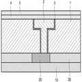
도 1 내지 도 8은 본 발명의 기술적 사상에 의한 실시예들에 따른 금속 배선 형성 방법(및 반도체 제조 장치의 제조 방법)을 개략적으로 나타내는 단면도들이다.
먼저 도 1을 참조하면, 기판(10) 상에 회로 요소(20)가 형성된다. 비록 도면에는 회로 요소(20)가 단순한 사각 형태로 표현되었지만, 회로 요소(20)는 다양한 형상을 가질 수 있다. 예를 들어 회로 요소(20)는 메모리 소자의 게이트 구조물 또는 커패시터 구조물일 수도 있고, 이미지 소자의 포토다이오드 또는 구동 트랜지스터일수도 있다. 회로 요소(20)의 주변에는 절연층(30)이 형성될 수 있다.
비록 도면에는 회로 요소(20)가 기판(10)으로부터 돌출된 구조물로 도시되었지만, 회로 요소(20)는 기판(10) 내로 형성된 도핑 영역일 수도 있고, 기판(10) 내부에 형성된 구조물(예를 들어 매립된 게이트 구조물)일 수도 있다. 이 경우 절연층은 기판(10)에 포함되는 구성요소가 될 것이다.
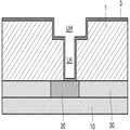
도 2를 참조하면, 회로 요소(20) 상에 층간 절연층(1)이 형성된다. 층간 절연층(1)은 절연층(30) 상에 형성될 수 있다. 선택적인 실시예에서, 층간 절연층(1)은 절연층(30)과 동시에 형성될 수도 있다. 층간 절연층(1)의 두께는 비아 구조물에 적합한 두께를 얻도록 증착될 수 있다.
도 3을 참조하면, 층간 절연층(1)을 식각하여 회로 요소(20)를 노출시킨다. 도 3에는 이중 트렌치의 비아 홀 구조(즉, 상부 홀(UH)과 하부 홀(LH)의 두께가 다른 홀 구조)가 도시되었지만, 비아 홀 구조는 그에 제한되지 않음에 유의한다. 비아 홀 구조는 단일 트렌치의 형상을 가질 수도 있고, 다중 트렌치의 형상을 가질 수도 있다.
이중 트렌치의 비아 홀 구조를 형성하기 위해, 다음과 같은 공정이 이용될 수 있다.
- 제1 단계 : 층간 절연층(1) 상에 제1 두께의 오프닝을 갖는 제1 감광 패턴을 형성
- 제2 단계 : 상기 제1 감광 패턴을 마스크로 층간 절연층(1)을 1차 식각하여 상기 제1 두께를 갖는 상부 홀(UH)을 형성
- 제3 단계 : 상부 홀(UH)의 측벽과 접촉하며 상부 홀(UH) 하면 일부를 노출시키는 제2 감광 패턴을 형성
- 제4 단계 : 상기 제2 감광 패턴을 마스크로 층간 절연층(1)을 2차 식각하여 상기 제1 두께보다 작은 제2 두께를 갖는 하부 홀(LH)을 형성
- 제5 단계 : 상기 제2 감광 패턴(및 상기 제1 감광 패턴)을 제거
전술한 공정은 단지 예시일 뿐이며, 이중 트렌치의 비아 홀 구조를 형성하기 위해 다른 공정이 적용될 수도 있다. 예를 들어 층간 절연층(1)을 형성하는 공정 동안, 하부 층간 절연층을 형성하고, 상기 하부 층간 절연층 상에 제2 두께의 오프닝을 갖는 식각 저지층을 형성한 후, 식각 저지층 상에 상부 층간 절연층을 형성할 수 있다. 이 경우 상부 층간 절연층을 식각하면 식각 저지층 및 제2 두께의 오프닝이 노출되게 되는데, 식각 저지층 아래의 하부 절연층은 식각이 이루어지지 않지만 오프닝 아래의 하부 절연층은 식각된다. 따라서 상기 상부 층간 절연층에는 제1 두께를 갖는 상부 홀이 형성되고 상기 하부 층간 절연층에는 제2 두께를 갖는 하부 홀이 형성될 것이다.
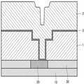
도 4를 참조하면, 이중 트렌치의 비아 홀 상에 확산 방지층(3)을 형성한다. 확산 방지층(3)은 비아 구조물의 금속 원소가 주변의 층간 절연층(1)으로 확산하는 것을 방지하는 역할을 할 수 있다. 확산 방지층(3)은 예를 들어 Ta, TaN, Ti, TiN, W, WN, TaSiN, TiSiN, 및 WSiN 중 적어도 하나를 포함할 수 있다.
도 5를 참조하면, 확산 방지층(3) 상에 금속층(2)을 형성한다. 금속층(2)은 예를 들어 구리를 포함할 수 있고, 주변 물질과의 열팽창 계수 차를 고려하여 기타 다른 금속 물질로 형성될 수도 있다. 비록 도 5에 도시되지는 않았지만, 예를 들어 구리를 이용한 금속층(2) 형성 시 먼저 확산 방지층(3) 상에 구리 시드층이 형성되고, 상기 구리 시드층을 이용하여 금속층이 형성될 수도 있다.
도 6을 참조하면, 평탄화 공정(Planarization process)을 이용하여 금속층(2) 일부를 제거하여 금속층(2)의 상부 표면을 평탄화시킨다. 상기 평탄화를 위해 화학 기계 연마(Chemical Mechanical Polishing, CMP) 공정이 이용될 수 있다.
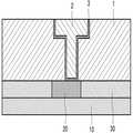
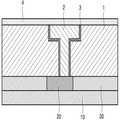
도 7 및 도 8을 참조하면, 평탄화 공정이 진행된 금속층(2) 상에 이중 층 구조의 캡핑층이 형성될 수 있다. 상기 캡핑층은 후속 배선 공정에서 건식 식각 가스, 수분(H2O), 산소(O2), 또는CMP등에 사용되는 수용성 화학종 등이 층간 절연층(1) 또는 구리 배선으로 확산/침투하는 것(in-diffusion)을 막는 역할을 할 수 있다.
상기 수분 혹은 산소가 층간 절연층(1)에 침투할 경우, 층간 절연층(1)의 유전율이 증가하고 RC 지연이 증가하면서 소자의 응답 속도가 감소하는 문제가 발생할 수 있다. 본 발명의 기술적 사상에 따르면, 상기 이중층 구조의 캡핑층을 도입함으로써, 그러한 문제가 방지될 수 있다. 또한, 캡핑층은 2개의 금속 층을 형성하기 위해 하부 금속층(2) 상에 상부 층간 절연층이 형성되는 경우, 하부 금속층(2)에서 상부 층간 절연층(1)으로 금속 성분이 확산(out-diffusion)되는 것을 막는 역할도 하며, 금속층(2)이 부식되는 것을 방지하는 역할도 수행할 수 있다.
본 발명자는, 기존의 SiCN 단일층으로 구성된 캡핑층이 소자의 크기가 감소함에 따라(그리고 캡핑층의 두께가 얇아짐에 따라) 수분이나 습기에 대한 차폐특성이 감소하게 된다는 문제점을 인식하고, 얇은 두께의 캡핑층에서도 우수한 차폐특성을 가질 수 있는 막을 증착하는 방법을 발명하였다.
이러한 방법의 일 예로서, 다음과 같은 공정이 수행될 수 있다.
- 금속층(2) 상에 제1 층(4)을 증착하는 단계(도 7 참조)
- 제1 층(4) 상에 제2 층(5)을 증착하는 단계(도 8 참조)
상기 제1 층(4) 및 제2 층(5)의 두께의 합은 100 Å 이하일 수 있다. 또한, 상기 제1 층(4) 및 제2 층(5)은 예를 들어 모두 질화층일 수 있다. 따라서, 본 발명의 기술적 사상에 따른 이중 층 구조의 캡핑층을 형성하는 단계는, 제1 질화층 및 제2 질화층을 증착하는 단계를 포함할 수 있다. 제1 질화층 및 제2 질화층은 순차로 증착될 수 있으며, 예를 들어 동일한 반응기에서 인-시튜(in-situ)로 형성될 수도 있다.
바람직한 실시예에서, 상기 제1 층(4)은 질화알루미늄(AlN) 층이고, 상기 제2 층(5)은 질화실리콘(SiN) 층일 수 있다. 예를 들어, 질화알루미늄(AlN) 층은 플라즈마 원자 층 증착법(PEALD)을 이용하여 형성될 수 있다. 또한, 질화실리콘(SiN) 층은 플라즈마 원자층 증착법(PEALD) 또는 펄스화된 플라즈마 화학 기상 증착법(Pulsed-PECVD, P-PECVD)을 이용하여 형성될 수 있다. 따라서 상기 캡핑층 형성 단계는 저온(예를 들어, 250 내지 350)의 온도 범위에서 진행될 수 있다.
PEALD 방법에서 전구체(precursor)와 플라즈마는 교대로, 단속적으로(intermittently) 반응기로 공급되는 과정을 반복할 수 있다. 한편 P-PECVD 방법에서는 플라즈마는 지속적으로 반응기로 공급되는 반면, 전구체(precursor)는 단속적으로(intermittently) 공급이 될 수 있다.
도 9는 본 발명의 기술적 사상에 의한 실시예들에 따른 금속 배선 형성 방법 및 반도체 제조 장치의 제조 방법을 개략적으로 나타내는 흐름도이다. 이 실시예들에 따른 제조 방법은 전술한 실시예들에 따른 제조 방법의 변형예일 수 있다. 이하 실시예들간 중복되는 설명은 생략하기로 한다.
도 9를 참조하면, 금속층(2) 상에 이중층 구조의 캡핑층을 형성하는 공정은 다음과 같은 단계로 수행될 수 있다.
제1 단계(S110) : 플라즈마 처리(plasma treatment),
제2 단계(S120) : PEALD에 의한 AlN 증착,
제3 단계(S130) : Pulsed PECVD에 의한 SiN증착
상기 제1 단계 내지 제3 단계(S110-S130)는 250내지 350의 온도 범위내의 동일 온도 조건에서 한 반응기에서 연속으로(in-situ) 진행한다.
먼저 제1 단계(S110)인 플라즈마 처리 공정은, 전공정 단계인 CMP (Chemical-Mechanical Planarization) 공정에서 금속층(2)(예를 들어, 구리 배선) 위에 형성된 산화금속(예를 들어, 산화 구리(CuO))을 금속(예를 들어, 구리(Cu))로 환원시키는 단계이다.
본 발명에서는 NH3, N2 및 H2의 혼합기체를 기판(10)이 탑재된 반응 공간으로 공급하면서 플라즈마를 활성화시킨다. 상기 플라즈마의 파워는 50W내지 300W의 범위일 수 있다. 상기 플라즈마 활성화에 의해 산화금속의 환원이 이루어짐과 동시에 평탄화된 금속층(도 6의 2) 표면에 잔류하는 공정 잔류물이 제거될 수 있다.
제1 단계(S110)는 플라즈마 활성화 단계 및 퍼지 단계의 사이클로 이루어지며, 본 실시예서는 상기 사이클을 1회만 진행하였다. 그러나 선택적인 실시예에서 상기 사이클은 복수 회 수행될 수도 있음에 유의한다.
상기 제1 단계(플라즈마 처리 단계)에서의 공정 조건을 요약하면 다음과 같다.
- 공정 온도 : 250 ~350
- 반응 기체 : N2/H2/NH3 (혼합 기체)
- 플라즈마 파워 : 100~300W
- 공정 압력 : 2~4 Torr
- 공정 시퀀스(sequence) : 플라즈마 점화(Plasma ignition) / 퍼지(Purge)
- 반복 횟수 : 1 사이클(cycle)
본 실시예에서는 반응 공간 내에서 플라즈마를 발생시키는 방법을 사용하였으나, 선택적인 실시예에 따르면, 리모트 플라즈마로 활성종을 생성시켜 상기 활성종이 반응 공간내로 공급됨으로써 플라즈마 처리 단계가 수행될 수도 있다.
제2 단계(S120)인 AlN 층 증착은 PEALD방법에 의해 진행된다. 본 실시예에서는, Al 소스로서 TMA(Trimethyl aluminum; Al(CH3)3)가 사용되었고 반응기체로는 N2/H2 혼합 기체가 사용되었다. AlN 층 증착은 TMA 공급 / 퍼지 / N2/H2 혼합 기체와 함께 플라즈마 공급 / 퍼지로 구성된 4단계를 일 사이클로 하여, 본 실시예에서는 AlN층이 20 Å의 두께가 될 때까지 상기 사이클을 18회 반복하였다. 본 실시예 에서는 상기 기본 사이클을18회 반복하였다.
상기 제2 단계(AlN 층 증착 단계)에서의 공정 조건을 요약하면 다음과 같다.
- 공정 온도 : 250 ~350
- 소스 기체 : TMA(trimethylaluminum)
- 반응 기체 : N2/H2 (혼합 기체)
- 퍼지 기체 : Ar
- 플라즈마 파워 : 200~400W
- 공정 압력 : 2~4 Torr
- 공정 시퀀스 : TMA 공급 / 퍼지 / 플라즈마 점화 / 퍼지
- 반복 횟수 : 18 사이클 (20 Å)
본 실시예에서는 반응 공간 내에서서 플라즈마를 발생시키는 방법을 사용하였으나, 전술한 바와 같이, 리모트 플라즈마로 활성종을 생성시켜 상기 활성종이 반응 공간내로 공급됨으로써 플라즈마 처리 단계가 수행되는 선택적인 실시예가 이용될 수도 있다.
제3 단계(S130)인 SiN 층 증착은 Pulsed PECVD 방법에 의해 진행된다. 본 실시예에서는 Si 소스로서 실란(SiH4)을 사용하였고 반응기체로는 N2/H2 혼합 기체를 사용하였다. 본 실시예에서, SiN 층 증착은 반응기체, 퍼지기체, 및 플라즈마를 지속적으로 공급하면서, 실란(SiH4)을 단속적으로 공급하였다. 바람직한 실시예에서, 실란(SiH4)은 0.2초간 공급되고, 퍼지기체는 2초간 공급하는 것을 1 사이클로 하여, SiN층이 30Å의 두께가 될 때까지 상기 사이클을 반복(50회)하였다.
상기 제3 단계(SiN 층 증착 단계)에서의 공정 조건을 요약하면 다음과 같다.
- 공정 온도 : 250 ~350
- 소스 기체 : SiH4
- 반응 기체 : N2/H2 (혼합 기체)
- 퍼지 기체 : Ar
- 플라즈마 파워 : 20-50W
- 공정 압력 : 2~4 Torr
- 공정 시퀀스 : SiH4 공급 / 퍼지
- 반복 횟수 : 50 사이클 (30Å)
본 실시예에서는 반응 공간 내에서서 플라즈마를 발생시키는 방법을 사용하였으나, 전술한 바와 같이, 리모트 플라즈마로 활성종을 생성시켜 상기 활성종이 반응 공간내로 공급됨으로써 플라즈마 처리 단계가 수행되는 선택적인 실시예가 이용될 수도 있다. 또한 본 실시예에 실란 계열의 소스기체로서 SiH4가 사용되었으나, SiH4 외에 다른 실란 계열의 소스 기체가 사용될 수 있다. 즉, 제3 단계(S130)의 소스 기체로서, 예를 들어 BDEAS(bisdiethylaminosilane), BEMAS(bisethylmethylaminosilane), DIPAS(diisoprophylaminosilane) 등을 포함하는 아미노실란(aminosilane)계열의 실리콘 소스기체, DCS(dichlorosilane), TCS(trichlorosilane), HCD(hexachlorodisilane)등을 포함하는 염화실란계열의 실리콘 소스 기체, 또는 이들의 조합이 사용될 수 있다.
전술한 실시예에 따르면, 캡핑층으로서 AlN/SiN이중 층 구조를 증착함으로써, 투습 방지 특성 평가시 우수한 특성을 확인할 수 있었다. 금속(구리) 배선 공정에서 저유전율 층간 절연층으로의 습기 침투 방지 및 구리의 층간 절연층으로의 확산이 방지될 수 있다. 즉, 발명자는 기존의 두꺼운 SiCN층 대신 얇은 AlN/SiN 층을 구현하고 이를 통해 우수한 투습 방지 특성을 확보함으로써, 소자크기가 축소됨에 따라 요구되는 100Å이하의 두께를 갖는 박막 형성이 달성될 수 있음을 발견하였다.
또한, 전술한 실시예에 따르면, 기존의 열공정(thermal process)대신 플라즈마 공정을 적용함으로써, 보다 저온에서 하부 저유전율(low-k) 층의 변형 및 손상이 최소화될 수 있다. 이외에 PEALD공정으로 막을 증착함으로써, 기존의 CVD에 의한 막보다 더욱 치밀하고 균일한 막을 증착할 수 있고, 보다 얇은 두께에서 보다 우수한 투습 방지 특성을 가진 박막을 증착할 수 있다. 이러한 효과를 보다 효율적으로 달성하기 위한 플라즈마 파워의 비율은 전술한 실시예에서 얻어진 수치와 같다. 즉, AlN 층 증착 단계 동안 공급되는 플라즈마 파워로서 200 내지 400W가 되고, SiN 층 증착 단계 동안 공급되는 플라즈마 파워로서 20 내지 50W가 되는 것이 그것이다. 발명자는 이러한 플라즈마 파워의 비율이 상기 AlN 층 증착 단계 동안 공급되는 플라즈마 파워 및 상기 SiN 층 증착 단계 동안 공급되는 플라즈마 파워의 비율로서 10:1 내지 8:1이 되는 것이 최적임을 발견하였다.
이외에도, 전술한 실시예에 따르면, 하나의 반응기에서 인-시튜(in-situ) 연속 공정으로 이중-층(bi-layer)을 증착함으로써, 대기에 노출 및 그에 의한 변형 없이 우수한 투습방지 특성을 가진 막이 증착될 수 있다.
도 10은 본 발명의 기술적 사상에 의한 실시예들에 따른 금속 배선 형성 방법 및 반도체 제조 장치의 제조 방법을 개략적으로 나타내는 흐름도이다. 이 실시예들에 따른 제조 방법은 전술한 실시예들에 따른 제조 방법의 변형예일 수 있다. 이하 실시예들간 중복되는 설명은 생략하기로 한다.
도 10을 참조하면, 제1 단계(S110)는 t0 내지 t2 시간 동안 이루어지는 플라즈마 처리(plasma treatment) 단계이다. 제1 단계(S110) 동안, CMP전공정(forward process)에 의해 금속배선(예를 들어, 구리배선) 표면 상에 형성된 산화금속(예를 들어, 산화구리)을 금속 원소로 환원시키는 과정이다.
예를 들어, 금속배선으로서 구리배선이 사용될 수 있고, 반응 기체로서 불활성 퍼지기체(예를 들어 N2)가 사용될 수 있다. 이 경우 소스기체(예를 들어 전구체)는 공급되지 않을 것이다.
선택적인 실시예에서, 반응 기체로서 NH3가 공급될 수 있고, 이를 플라즈마로 활성화시켜 산화구리가 환원될 수 있다. 이 경우 퍼지 기체가 별도로 공급될 수도 있을 것이다.
상기 제1 단계(S110)는 x회 반복될 수 있으나, 본 발명에 따른 한 실시예에서 상기 제1 단계(S110)는 1회만 진행되었다.
제2 단계(S120)는 t2 내지 t6 시간 동안 진행되는 PEALD 증착 공정이다. 상기 제2 단계(S120) 동안, 소스기체인 전구체(precursor) 및 반응기체(reactant)가 순차적으로 공급될 수 있다. 보다 구체적으로 t2 내지 t3 시간 동안 소스 기체가 공급되고, t4 내지 t5 시간 동안 반응 기체가 공급될 수 있다. 퍼지 기체는 t2 내지 t6 시간 동안 공급될 수 있다.
t4 내지 t5의 시간 동안 플라즈마가 공급되면서 반응기체가 활성화(activation)될 수 있고, 이렇게 활성화된 반응 기체는 미리 원자 층 단위의 두께로 증착된 소스기체와 반응하여 기판(10) 상에 막이 증착될 수 있다. 예시적인 실시예에서, 상기 제2 단계(S120) 동안, 소스기체로 TMA(trimethylaluminum; Al(CH3)3), 반응기체로 질소(N2)와 수소(H2)의 혼합기체 혹은 NH3를 사용하여 AlN층이 증착될 수 있다.
상기 t2 내지 t6시간 동안 이루어지는 단계들을 하나의 사이클로 하여, m회 반복하여 복수의 원자층이 증착될 수 있다. 바람직하게는, 상기 사이클이 반복되어 10 Å 이상의 두께를 갖는AlN층이 증착될 수 있다. 더욱 바람직하게는 AlN층은 20 Å 내지 30 Å의 두께를 갖도록 형성될 수 있다.
비록 도 10에는 상기 제2 단계(S120) 동안 반응 기체가 플라즈마가 공급되는 t4 내지 t5 시간 동안(즉, t4 이후에) 공급되는 것으로 도시되어 있지만, 상기 반응 기체는 플라즈마가 공급되는 시점인 t4 이전부터 공급될 수도 있다. 따라서, 반응 공간 내에 반응기체 밀도가 보다 균일해질 수 있다. 따라서, 상기 t4 이전의 시점에서 반응기체가 공급됨으로써, 반응공간 내에 활성종 밀도가 균일해지고 증착되는 막의 특성, 예를 들어 WERR(Wet Etch Rate Ratio)이 보다 균일해 질 수 있다.
일부 실시예들에서 퍼지 기체로서 아르곤(Ar) 등의 불활성 기체가 사용될 수 있다. 퍼지 기체는 t2내지 t6의 기간 동안 지속적으로 반응기로 공급될 수 있다. 이 경우 전술한 바와 같이 반응기체로서 질소(N2)와 수소(H2)의 혼합기체 혹은 암모니아(NH3)가 공급될 수 있다.
선택적인 실시예에서, 퍼지 기체로서 질소(N2)기체가 사용될 수도 있다. 질소 기체는 반응성 퍼지기체(reactive purge gas)로 사용될 수도 있고, 이 경우 질소 기체는 플라즈마가 공급될 때에만 활성화되어 소스기체와 반응을 하여 AlN층을 형성할 수 있다.
제3 단계(S130)는 SiN 박막을 증착하는 단계로서, 펄스화된(Pulsed) PECVD 방법을 이용하여 증착될 수 있다. 상기 펄스화된 PECVD 방법에 의한 증착은 제2 단계(S120)의 PEALD 방법에 의한 증착이 이루어지는 반응기와 동일한 반응기에서 인-시튜(in-situ)로 진행될 수 있다.
전술한 제2 단계(S120)에서 증착되는 AlN층은 대기에 노출시 산화될 수 있다. 따라서 동일한 반응기에서 계속적으로 제3 단계(S130)를 진행하여 AlN/SiN층이 인-시튜(in-situ)로 증착될 수 있다.
상기 제3 단계(S130)에서 반응기체, 퍼지기체 그리고 플라즈마는 t6 내지 t10시간 동안 지속적으로 공급되는 반면, 소스기체는 t7시간 동안 단속적으로 공급된다. 상기 t6 내지 t10기간을 일 사이클로 하여 상기 사이클을 n회 반복하면서 원하는 두께의 SiN 박막이 증착될 수 있다. 제3 단계(S130)에서, 반응기체로서 질소(N2)와 수소(H2)의 혼합기체 혹은 암모니아(NH3)가 사용될 수 있다. 일 실시예에서, SiN 박막은 30Å 이상의 두께로 증착될 수 있다. 바람직한 실시예에서, SiN 박막은 30Å 내지 60Å의 두께로 증착될 수 있다.
전술한 바와 같이 AlN 층은 20 Å 내지 30 Å의 두께를 갖고, SiN 박막은 30Å 내지 60Å의 두께를 가질 수 있으므로, AlN 층의 두께와 상기 SiN 층의 두께의 비율은 1:1.5 내지 1:2일 수 있다. 다만 이러한 AlN 층의 두께와 상기 SiN 층의 두께 그리고 이들 간의 비율은 100 Å 미만의 설계가 요구되는 공정조건을 충족하기 위해(그러면서도 우수한 차폐특성을 갖도록) 도입된 조건이다(도 13 참조). 따라서 본 발명의 기술적 사상에 따른 이중막 구조의 개별 두께(즉, 개별 층의 두께)가 전술한 수치에 제한되지 않음에 유의한다.
선택적인 실시예에서, 상기 제1 단계 내지 제3 단계(S110-S130) 동안, 공정 온도는 250~350 범위의 저온으로 유지될 수 있다. 따라서 다충 금속층 구조물을 형성하는 동안, 하부의 층간 절연층(특히 저유전율 층)의 손상이 방지될 수 있다. 또한, 상기 제1 내지 제3 단계들 동안 플라즈마가 인가됨으로써 반응속도가 빨라져, 기존의 열반응 공정(thermal ALD process) 대비 증착 속도가 개선되어 단위 시간당 생산성이 높아지는 효과가 달성될 수 있다. 또한 사이클 단위로 낮은 두께의 박막을 증착함으로써 박막 균일도가 개선될 수 있다.
도 11 및 도 12는 본 발명의 기술적 사상에 의한 또다른 실시예들에 따른 반도체 장치의 금속 배선 부분을 개략적으로 나타낸 단면도들이다. 이 실시예들에 따른 금속 배선 내지 금속 배선을 포함하는 반도체 장치는 전술한 실시예들에 따른 제조 방법이 적용되어 형성된 구조물일 수 있다. 이하 실시예들간 중복되는 설명은 생략하기로 한다.
도 11을 참조하면, 금속 배선은 예를 들어 구리 배선일 수 있고, 로직 소자 또는 메모리 소자에 적용될 수 있다. 상기 금속 배선은 저 유전율 층(low-k dielectric layer)인 층간 절연층(1), 금속층(2), 확산 방지층(3), 및 캡핑층을 포함할 수 있다.
층간 절연층(1)은 예를 들어 2.5 이하의 저유전율을 갖는 물질로 형성될 수 있고, 예를 들어 TEOS(tetra ethoxy ortho silicate; Si(C2H5O)4) 기반의 물질(예를 들어 SiOC, SICOH 등)을 포함할 수 있다. 층간 절연층(1)은 다공성 구조를 가질 수 있다. 층간 절연층(1)은 금속층(2)과 확산 방지층(3)의 측면을 둘러쌀 수 있다.
확산 방지층(3)은 전술한 바와 같이 금속층(2)의 금속 원소가 확산되어 층간 절연층(1)의 막질에 영향을 주는 것을 방지하는 역할을 수행할 수 있다. 금속층(2)은 알루미늄 내지 구리와 같은 배선층으로서, 확산 방지층(3)과 금속층(2)을 하나의 구성요소로 지칭할 수도 있을 것이다(예를 들어, 금속층(2)으로 지칭).
캡핑층은 전술한 바와 같이 제1 층(4) 및 제2 층(5)으로 구성된 이중층 구조이며, 제1 질화층(예를 들어 질화알루미늄 층) 및 제2 질화층(예를 들어 질화실리콘 층)을 포함할 수 있다. 제1 층은 금속층(2)의 적어도 일부(예를 들어, 상면) 및 층간 절연층(1)과 접촉할 수 있다. 상기 접촉은 직접적인 접촉(즉, 2개의 구성요소 사이에 여하의 구성요소가 없는 접촉)일 수 있다. 제2 층은 제1 층 상에 위치될 수 있고, 선택적인 실시예에서 제1 층과 제2 층이 인-시튜로 형성됨으로써 양자가 직접적으로 접촉할 수 있다.
도 12는 2층의 배선 구조를 나타낸 것으로 도 11의 배선 구조(즉, 제1 금속층(2)) 상에 추가 배선 구조(즉, 제2 금속층(2'))가 형성된 모습을 나타낸다.
도 12를 참조하면, 제2 금속층(2')은 제1 금속층(2) 상에 형성될 수 있다. 보다 구체적으로, 예를 들어 제1 층이 질화알루미늄 층이고 제2 층이 질화실리콘 층인 경우, 제2 금속층(2')은 상기 제1 금속층(2)의 상면, 상기 질화알루미늄 층의 측면, 및 상기 질화실리콘 층의 측면과 접촉할 수 있다.
비록 도 12와 본 실시예에서는 제2 금속층이 부재번호 2'로 지칭되었지만, 금속층(또는 제2 금속층)은 부재번호 2'에 제한되어 해석되지 않음에 유의한다. 예를 들어, 전술한 바와 같이 상기 제2 금속층은 금속을 포함하는 확산 방지층(3')을 포함하는 것으로 해석될 수도 있다. 이 경우 제2 금속층은 상기 제1 금속층(2)의 상면, 상기 질화알루미늄 층의 측면, 및 상기 질화실리콘 층의 측면과 직접 접촉할 수 있다.
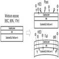
도 13은 하부 기판 상에서 본 발명에 따른 이중 층 구조가 적절한 차폐 특성을 갖는지를 파악하기 위한 실험을 나타낸다. 하부의 기판은 전술한 실시예들에 따른 금속층과 확산 방지층 및 층간 절연층(특히 TEOS)으로 구성된 구조이다. 특히 TEOS의 경우 물을 아주 잘 흡수하는데, 이러한 수분의 흡수로 인해 하부 기판의 부피가 팽창하게 되어 압축 응력이 발생하게 된다(우하단 Fail 부분 참조).
투습을 방지하기 위한 캡핑층의 조건으로, 85의 온도 및 85%의 습도 분위기에 17시간 동안 노출될 경우, 기판의 스트레스의 변화가 50Mpa 미만이 되어야 한다. 일반적으로 캡핑층의 두께가 작아질수록 투습에 취약하며, 종래의 SiCN 캡핑층은 100 Å 이하의 두께로 구현될 경우 전술한 조건 하에서의 스트레스 변화 차이가 50 Mpa 미만이 되도록 하는 요건을 만족하지 못하였다.
그러나 본 발명의 기술적 사상에 의한 실시예들에 따르면, 서로 다른 물질의 이중 층 구조를 도입함으로써, 이러한 스트레스 변화 조건이 만족될 수 있도록 하였다.
아래 표 1은 도 13의 실험을 본 발명 기술적 사상에 의한 실시예들 중 일 실시예에 의해 형성된 이중층 구조(AlN 20Å / SiN 30Å)에 대해 수분(H2O)에 대한 투습 방지특성(hermetic feature)의 평가 결과를 보여 준다.
| Slot No. | AlN 두께 | SiN 두께 | Si 전구체 | 스트레스 변화(△MPa) | Pass/Fail |
| 01 | 20 | 30 | BDEAS | -38 | Pass |
| 02 | 20 | 40 | BDEAS | -40 | Pass |
| 03 | 20 | 30 | SiH4 | -4 | Pass |
| 04 | 20 | 40 | SiH4 | -5 | Pass |
위 표 1에서 알 수 있듯이, 기존 SiCN층의 경우 100Å두께 이하에서 투습 방지 특성이 저하되는 것과 비교할 때 본 발명은 그보다 낮은 두께에서도 우수한 투습 방지 특성을 나타냄을 알 수 있다.
본 발명을 명확하게 이해시키기 위해 첨부한 도면의 각 부위의 형상은 예시적인 것으로 이해하여야 한다. 도시된 형상 외의 다양한 형상으로 변형될 수 있음에 주의하여야 할 것이다.
이상에서 설명한 본 발명이 전술한 실시예 및 첨부된 도면에 한정되지 않으며, 본 발명의 기술적 사상을 벗어나지 않는 범위 내에서 여러 가지 치환, 변형 및 변경이 가능하다는 것은, 본 발명이 속하는 기술분야에서 통상의 지식을 가진 자에게 있어 명백할 것이다.
Claims (21)
- 저 유전층(low-k dielectric layer) 증착 단계;
상기 저 유전층에 트렌치(trench)를 형성하는 단계;
상기 트렌치에 배리어층(barrier layer)를 형성하는 단계;
상기 배리어 층 상에 금속을 충진하는 단계;
상기 금속에 대한 평탄화(planarization) 단계; 및
상기 평탄화된 금속 상에 캡핑층(capping layer)을 형성하는 단계;를 포함하고,
상기 캡핑층은 적어도 2개의 층을 포함하고, 100 Å이하의 두께를 갖는 것을 특징으로 하는 금속 배선 형성 방법. - 청구항 1에 있어서,
상기 캡핑층을 형성하는 단계는,
제1 질화층 및 제2 질화층을 증착하는 단계;를 포함하는 금속 배선 형성 방법. - 청구항 2에 있어서,
상기 제1 질화층 및 제2 질화층을 증착하는 단계는,
AlN 층 증착 단계; 및
SiN 층 증착 단계;를 포함하는 것을 특징으로 하는 금속 배선 형성 방법. - 청구항 3에 있어서,
상기 AlN 층은 플라즈마 원자 층 증착법(PEALD)을 이용하여 형성되는 것을 특징으로 하는 금속 배선 형성 방법. - 청구항 4에 있어서,
상기 AlN 층 증착 단계는 복수의 사이클들을 포함하고,
상기 복수의 사이클들 각각은,
Al 소스 기체 공급단계;
퍼지 기체 공급 단계;
반응 기체를 공급하고 플라즈마로 상기 반응 기체를 활성화하는 단계; 및
퍼지 기체 공급 단계;를 포함하고,
상기 퍼지 기체는 상기 사이클들 동안 반응 공간에 지속적으로 공급되는 것을 특징으로 하는 금속 배선 형성 방법. - 청구항 5에 있어서,
상기 Al 소스기체는 TMA(TriMethyl Aluminaum, Al(CH3)3)를 포함하고, 상기 반응 기체는 질소 및 수소의 혼합 기체를 포함하는 것을 특징으로 하는, 금속 배선 형성 방법. - 청구항 3 또는 청구항 4에 있어서,
상기 SiN 층은 펄스화된 플라즈마 화학 기상 증착법(pulsed PECVD)을 이용하여 형성되는 것을 특징으로 하는 금속 배선 형성 방법 - 청구항 7에 있어서,
상기 SiN 층 증착 단계는 복수의 사이클들을 포함하고,
상기 복수의 사이클들 각각은,
Si 소스 기체 공급 단계;
퍼지 기체 공급 단계;
반응 기체 공급하고 플라즈마로 상기 반응 기체를 활성화하는 단계; 및
퍼지 기체 공급 단계;를 포함하고,
상기 반응기체, 상기 퍼지 기체, 및 상기 플라즈마는 상기 사이클들 동안 반응 공간에 지속적으로 공급되는 것을 특징으로 하는 금속 배선 형성 방법. - 청구항 8에 있어서,
상기 Si 소스 기체는 Si와 H 원소를 포함하는 Si 소스 기체인 것을 특징으로 하는 금속 배선 형성 방법. - 청구항 9에 있어서,
상기 Si 소스 기체는 SiH4, BDEAS(Bis(diethylamino) Silane), 및 DIPAS(Diisopropylamino Silane) 중 적어도 하나를 포함하는 것을 특징으로 하는 금속 배선 형성 방법. - 청구항 8에 있어서,
상기 반응 기체는 질소 및 수소의 혼합 기체를 포함하는 것을 특징으로 하는 금속 배선 형성 방법. - 청구항 3에 있어서,
상기 SiN 층의 두께는 적어도 30 옹스트롬인 것을 특징으로 하는 금속 배선 형성 방법. - 청구항 3에 있어서,
상기 제1 질화층 및 제2 질화층을 증착하는 단계 전에 플라즈마 처리 단계를 포함하고,
상기 플라즈마 처리 단계는 적어도 하나의 사이클을 포함하며,
상기 사이클은,
질소 함유 기체 공급 단계;
플라즈마로 상기 질소 함유 기체를 활성화하는 단계; 및
퍼지 기체 공급 단계;를 포함하며,
상기 사이클에 의해, 금속 상부의 산화 금속이 금속으로 환원되는 것읕 특징으로 하는 금속 배선 형성 방법. - 청구항 3에 있어서,
상기 캡핑층 형성 단계는 250 ℃ 내지 350 ℃의 온도 범위에서 진행되는 것을 특징으로 하는 금속 배선 형성 방법. - 청구항 3에 있어서,
상기 제1 질화층 및 상기 제2 질화층은 동일한 반응기에서 인-시튜(in-situ)로 형성되는 것을 특징으로 하는 금속 배선 형성 방법. - 청구항 4에 있어서,
상기 AlN 층의 두께와 상기 SiN 층의 두께의 비율은 1:1.5 내지 1:2인 것을 특징으로 하는 금속 배선 형성 방법. - 청구항 16에 있어서,
상기 AlN 층 및 상기 SiN 층을 포함하는 상기 캡핑층은, 섭씨 85도의 온도 및 85%의 습도 조건에서 17시간 동안 노출된 경우, 50MPa 이하의 박막 스트레스 변화량을 갖는 것을 특징으로 하는 금속 배선 형성 방법. - 청구항 4에 있어서,
상기 AlN 층 증착 단계 동안 공급되는 플라즈마 파워 및 상기 SiN 층 증착 단계 동안 공급되는 플라즈마 파워의 비율은 10:1 내지 8:1인 것을 특징으로 하는 금속 배선 형성 방법. - 저 유전층(low-k dielectric film) 증착 단계;
상기 저 유전층에 트렌치(trench)를 형성하는 단계;
상기 트렌치에 배리어 층(barrier film)을 형성하는 단계;
상기 배리어 층 상에 구리를 충진하여 구리층을 형성하는 단계;
상기 구리층에 대한 평탄화(planarization)를 수행하는 단계;
상기 평탄화된 구리층에 플라즈마를 인가하는 단계;
플라즈마 증강 원자층 증착(Plasma Enhanced Atomic Layer Deposition, PEALD) 방법을 이용하여, 상기 평탄화된 구리층 상에 AlN 층을 형성하는 단계; 및
상기 AlN 층을 형성한 반응기와 동일한 반응기에서 인-시튜(in-situ)로, 상기 AlN 층 상에 SiN 층을 형성하는 단계를 포함하고,
상기 AlN 층의 두께 및 상기 SiN 층의 두께의 합은 50 Å 내지 100 Å 이며,
상기 AlN 층의 형성 단계 및 상기 SiN 층의 형성 단계는 250 ℃ 내지 350 ℃의 온도범위에서 수행되는 것을 특징으로 하는, 반도체 장치의 제조 방법. - 반도체 장치의 제조 방법으로서,
제1 유전층을 형성하는 단계;
상기 제1 유전층 내에 제1 금속층을 형성하는 단계; 및
상기 제1 유전층 및 상기 제1 금속층 상에 100 Å 미만의 두께를 갖는 캡핑층을 형성하는 단계를 포함하고,
상기 캡핑층을 형성하는 단계는,
질화알루미늄 층을 형성하는 제1 단계; 및
상기 질화알루미늄 층 상에 질화실리콘 층을 형성하는 제2 단계를 포함하는 것을 특징으로 하는, 방법. - 제1 금속층;
상기 제1 금속층의 측면을 둘러싸는 제1 유전층;
상기 제1 금속층의 적어도 일부 및 상기 제1 유전층과 접촉하는 질화알루미늄 층;
상기 질화알루미늄 층 상의 질화실리콘 층;
상기 제1 금속층의 상면, 상기 질화알루미늄 층의 측면, 및 상기 질화실리콘 층의 측면과 접촉하는 제2 금속층; 및
상기 제2 금속층의 측면을 둘러싸는 제2 유전층을 포함하고,
상기 질화알루미늄 층의 두께 및 상기 질화실리콘 층의 두께의 합은 100 Å 미만인 것을 특징으로 하는, 반도체 장치.
Priority Applications (4)
| Application Number | Priority Date | Filing Date | Title |
|---|---|---|---|
| KR1020160060210AKR102592471B1 (ko) | 2016-05-17 | 2016-05-17 | 금속 배선 형성 방법 및 이를 이용한 반도체 장치의 제조 방법 |
| US15/499,647US10249577B2 (en) | 2016-05-17 | 2017-04-27 | Method of forming metal interconnection and method of fabricating semiconductor apparatus using the method |
| TW106115573ATWI643292B (zh) | 2016-05-17 | 2017-05-11 | 形成金屬內連線的方法以及使用該方法製造半導體裝置的方法 |
| CN201710345544.5ACN107393867B (zh) | 2016-05-17 | 2017-05-16 | 形成金属内连线的方法和使用其制造半导体装置的方法 |
Applications Claiming Priority (1)
| Application Number | Priority Date | Filing Date | Title |
|---|---|---|---|
| KR1020160060210AKR102592471B1 (ko) | 2016-05-17 | 2016-05-17 | 금속 배선 형성 방법 및 이를 이용한 반도체 장치의 제조 방법 |
Publications (2)
| Publication Number | Publication Date |
|---|---|
| KR20170129475Atrue KR20170129475A (ko) | 2017-11-27 |
| KR102592471B1 KR102592471B1 (ko) | 2023-10-20 |
Family
ID=60330372
Family Applications (1)
| Application Number | Title | Priority Date | Filing Date |
|---|---|---|---|
| KR1020160060210AActiveKR102592471B1 (ko) | 2016-05-17 | 2016-05-17 | 금속 배선 형성 방법 및 이를 이용한 반도체 장치의 제조 방법 |
Country Status (4)
| Country | Link |
|---|---|
| US (1) | US10249577B2 (ko) |
| KR (1) | KR102592471B1 (ko) |
| CN (1) | CN107393867B (ko) |
| TW (1) | TWI643292B (ko) |
Cited By (2)
| Publication number | Priority date | Publication date | Assignee | Title |
|---|---|---|---|---|
| KR20200001549A (ko)* | 2018-06-27 | 2020-01-06 | 타이완 세미콘덕터 매뉴팩쳐링 컴퍼니 리미티드 | 캐패시터를 포함하는 전자 디바이스 |
| KR20220035837A (ko)* | 2020-09-14 | 2022-03-22 | 에이에스엠 아이피 홀딩 비.브이. | 상향식 금속 나이트라이드 형성 |
Families Citing this family (364)
| Publication number | Priority date | Publication date | Assignee | Title |
|---|---|---|---|---|
| US10378106B2 (en) | 2008-11-14 | 2019-08-13 | Asm Ip Holding B.V. | Method of forming insulation film by modified PEALD |
| US9394608B2 (en) | 2009-04-06 | 2016-07-19 | Asm America, Inc. | Semiconductor processing reactor and components thereof |
| US8802201B2 (en) | 2009-08-14 | 2014-08-12 | Asm America, Inc. | Systems and methods for thin-film deposition of metal oxides using excited nitrogen-oxygen species |
| US9312155B2 (en) | 2011-06-06 | 2016-04-12 | Asm Japan K.K. | High-throughput semiconductor-processing apparatus equipped with multiple dual-chamber modules |
| US10364496B2 (en) | 2011-06-27 | 2019-07-30 | Asm Ip Holding B.V. | Dual section module having shared and unshared mass flow controllers |
| US10854498B2 (en) | 2011-07-15 | 2020-12-01 | Asm Ip Holding B.V. | Wafer-supporting device and method for producing same |
| US20130023129A1 (en) | 2011-07-20 | 2013-01-24 | Asm America, Inc. | Pressure transmitter for a semiconductor processing environment |
| US9017481B1 (en) | 2011-10-28 | 2015-04-28 | Asm America, Inc. | Process feed management for semiconductor substrate processing |
| US9659799B2 (en) | 2012-08-28 | 2017-05-23 | Asm Ip Holding B.V. | Systems and methods for dynamic semiconductor process scheduling |
| US10714315B2 (en) | 2012-10-12 | 2020-07-14 | Asm Ip Holdings B.V. | Semiconductor reaction chamber showerhead |
| US20160376700A1 (en) | 2013-02-01 | 2016-12-29 | Asm Ip Holding B.V. | System for treatment of deposition reactor |
| US9484191B2 (en) | 2013-03-08 | 2016-11-01 | Asm Ip Holding B.V. | Pulsed remote plasma method and system |
| US9589770B2 (en) | 2013-03-08 | 2017-03-07 | Asm Ip Holding B.V. | Method and systems for in-situ formation of intermediate reactive species |
| US9240412B2 (en) | 2013-09-27 | 2016-01-19 | Asm Ip Holding B.V. | Semiconductor structure and device and methods of forming same using selective epitaxial process |
| US10683571B2 (en) | 2014-02-25 | 2020-06-16 | Asm Ip Holding B.V. | Gas supply manifold and method of supplying gases to chamber using same |
| US10167557B2 (en) | 2014-03-18 | 2019-01-01 | Asm Ip Holding B.V. | Gas distribution system, reactor including the system, and methods of using the same |
| US11015245B2 (en) | 2014-03-19 | 2021-05-25 | Asm Ip Holding B.V. | Gas-phase reactor and system having exhaust plenum and components thereof |
| US10858737B2 (en) | 2014-07-28 | 2020-12-08 | Asm Ip Holding B.V. | Showerhead assembly and components thereof |
| US9890456B2 (en) | 2014-08-21 | 2018-02-13 | Asm Ip Holding B.V. | Method and system for in situ formation of gas-phase compounds |
| US10941490B2 (en) | 2014-10-07 | 2021-03-09 | Asm Ip Holding B.V. | Multiple temperature range susceptor, assembly, reactor and system including the susceptor, and methods of using the same |
| US9657845B2 (en) | 2014-10-07 | 2017-05-23 | Asm Ip Holding B.V. | Variable conductance gas distribution apparatus and method |
| KR102263121B1 (ko) | 2014-12-22 | 2021-06-09 | 에이에스엠 아이피 홀딩 비.브이. | 반도체 소자 및 그 제조 방법 |
| US10529542B2 (en) | 2015-03-11 | 2020-01-07 | Asm Ip Holdings B.V. | Cross-flow reactor and method |
| US10276355B2 (en) | 2015-03-12 | 2019-04-30 | Asm Ip Holding B.V. | Multi-zone reactor, system including the reactor, and method of using the same |
| US10458018B2 (en) | 2015-06-26 | 2019-10-29 | Asm Ip Holding B.V. | Structures including metal carbide material, devices including the structures, and methods of forming same |
| US10600673B2 (en) | 2015-07-07 | 2020-03-24 | Asm Ip Holding B.V. | Magnetic susceptor to baseplate seal |
| US9960072B2 (en) | 2015-09-29 | 2018-05-01 | Asm Ip Holding B.V. | Variable adjustment for precise matching of multiple chamber cavity housings |
| US10211308B2 (en) | 2015-10-21 | 2019-02-19 | Asm Ip Holding B.V. | NbMC layers |
| US10322384B2 (en) | 2015-11-09 | 2019-06-18 | Asm Ip Holding B.V. | Counter flow mixer for process chamber |
| US11139308B2 (en) | 2015-12-29 | 2021-10-05 | Asm Ip Holding B.V. | Atomic layer deposition of III-V compounds to form V-NAND devices |
| US10529554B2 (en) | 2016-02-19 | 2020-01-07 | Asm Ip Holding B.V. | Method for forming silicon nitride film selectively on sidewalls or flat surfaces of trenches |
| US10468251B2 (en) | 2016-02-19 | 2019-11-05 | Asm Ip Holding B.V. | Method for forming spacers using silicon nitride film for spacer-defined multiple patterning |
| US10501866B2 (en) | 2016-03-09 | 2019-12-10 | Asm Ip Holding B.V. | Gas distribution apparatus for improved film uniformity in an epitaxial system |
| US10343920B2 (en) | 2016-03-18 | 2019-07-09 | Asm Ip Holding B.V. | Aligned carbon nanotubes |
| US9892913B2 (en) | 2016-03-24 | 2018-02-13 | Asm Ip Holding B.V. | Radial and thickness control via biased multi-port injection settings |
| US10190213B2 (en) | 2016-04-21 | 2019-01-29 | Asm Ip Holding B.V. | Deposition of metal borides |
| US10865475B2 (en) | 2016-04-21 | 2020-12-15 | Asm Ip Holding B.V. | Deposition of metal borides and silicides |
| US10367080B2 (en) | 2016-05-02 | 2019-07-30 | Asm Ip Holding B.V. | Method of forming a germanium oxynitride film |
| US10032628B2 (en) | 2016-05-02 | 2018-07-24 | Asm Ip Holding B.V. | Source/drain performance through conformal solid state doping |
| KR102592471B1 (ko) | 2016-05-17 | 2023-10-20 | 에이에스엠 아이피 홀딩 비.브이. | 금속 배선 형성 방법 및 이를 이용한 반도체 장치의 제조 방법 |
| US11453943B2 (en) | 2016-05-25 | 2022-09-27 | Asm Ip Holding B.V. | Method for forming carbon-containing silicon/metal oxide or nitride film by ALD using silicon precursor and hydrocarbon precursor |
| US10388509B2 (en) | 2016-06-28 | 2019-08-20 | Asm Ip Holding B.V. | Formation of epitaxial layers via dislocation filtering |
| US10612137B2 (en) | 2016-07-08 | 2020-04-07 | Asm Ip Holdings B.V. | Organic reactants for atomic layer deposition |
| US9859151B1 (en) | 2016-07-08 | 2018-01-02 | Asm Ip Holding B.V. | Selective film deposition method to form air gaps |
| US10714385B2 (en) | 2016-07-19 | 2020-07-14 | Asm Ip Holding B.V. | Selective deposition of tungsten |
| KR102354490B1 (ko) | 2016-07-27 | 2022-01-21 | 에이에스엠 아이피 홀딩 비.브이. | 기판 처리 방법 |
| US9812320B1 (en) | 2016-07-28 | 2017-11-07 | Asm Ip Holding B.V. | Method and apparatus for filling a gap |
| US10395919B2 (en) | 2016-07-28 | 2019-08-27 | Asm Ip Holding B.V. | Method and apparatus for filling a gap |
| KR102532607B1 (ko) | 2016-07-28 | 2023-05-15 | 에이에스엠 아이피 홀딩 비.브이. | 기판 가공 장치 및 그 동작 방법 |
| US9887082B1 (en) | 2016-07-28 | 2018-02-06 | Asm Ip Holding B.V. | Method and apparatus for filling a gap |
| KR102613349B1 (ko) | 2016-08-25 | 2023-12-14 | 에이에스엠 아이피 홀딩 비.브이. | 배기 장치 및 이를 이용한 기판 가공 장치와 박막 제조 방법 |
| US10410943B2 (en) | 2016-10-13 | 2019-09-10 | Asm Ip Holding B.V. | Method for passivating a surface of a semiconductor and related systems |
| US10643826B2 (en) | 2016-10-26 | 2020-05-05 | Asm Ip Holdings B.V. | Methods for thermally calibrating reaction chambers |
| US11532757B2 (en) | 2016-10-27 | 2022-12-20 | Asm Ip Holding B.V. | Deposition of charge trapping layers |
| US10643904B2 (en) | 2016-11-01 | 2020-05-05 | Asm Ip Holdings B.V. | Methods for forming a semiconductor device and related semiconductor device structures |
| US10435790B2 (en) | 2016-11-01 | 2019-10-08 | Asm Ip Holding B.V. | Method of subatmospheric plasma-enhanced ALD using capacitively coupled electrodes with narrow gap |
| US10229833B2 (en) | 2016-11-01 | 2019-03-12 | Asm Ip Holding B.V. | Methods for forming a transition metal nitride film on a substrate by atomic layer deposition and related semiconductor device structures |
| US10714350B2 (en) | 2016-11-01 | 2020-07-14 | ASM IP Holdings, B.V. | Methods for forming a transition metal niobium nitride film on a substrate by atomic layer deposition and related semiconductor device structures |
| US10134757B2 (en) | 2016-11-07 | 2018-11-20 | Asm Ip Holding B.V. | Method of processing a substrate and a device manufactured by using the method |
| KR102546317B1 (ko) | 2016-11-15 | 2023-06-21 | 에이에스엠 아이피 홀딩 비.브이. | 기체 공급 유닛 및 이를 포함하는 기판 처리 장치 |
| US10340135B2 (en) | 2016-11-28 | 2019-07-02 | Asm Ip Holding B.V. | Method of topologically restricted plasma-enhanced cyclic deposition of silicon or metal nitride |
| KR102762543B1 (ko) | 2016-12-14 | 2025-02-05 | 에이에스엠 아이피 홀딩 비.브이. | 기판 처리 장치 |
| US11581186B2 (en) | 2016-12-15 | 2023-02-14 | Asm Ip Holding B.V. | Sequential infiltration synthesis apparatus |
| US11447861B2 (en) | 2016-12-15 | 2022-09-20 | Asm Ip Holding B.V. | Sequential infiltration synthesis apparatus and a method of forming a patterned structure |
| KR102700194B1 (ko) | 2016-12-19 | 2024-08-28 | 에이에스엠 아이피 홀딩 비.브이. | 기판 처리 장치 |
| US10269558B2 (en) | 2016-12-22 | 2019-04-23 | Asm Ip Holding B.V. | Method of forming a structure on a substrate |
| US10867788B2 (en) | 2016-12-28 | 2020-12-15 | Asm Ip Holding B.V. | Method of forming a structure on a substrate |
| US11390950B2 (en) | 2017-01-10 | 2022-07-19 | Asm Ip Holding B.V. | Reactor system and method to reduce residue buildup during a film deposition process |
| US10655221B2 (en) | 2017-02-09 | 2020-05-19 | Asm Ip Holding B.V. | Method for depositing oxide film by thermal ALD and PEALD |
| US10468261B2 (en) | 2017-02-15 | 2019-11-05 | Asm Ip Holding B.V. | Methods for forming a metallic film on a substrate by cyclical deposition and related semiconductor device structures |
| US10283353B2 (en) | 2017-03-29 | 2019-05-07 | Asm Ip Holding B.V. | Method of reforming insulating film deposited on substrate with recess pattern |
| US10529563B2 (en) | 2017-03-29 | 2020-01-07 | Asm Ip Holdings B.V. | Method for forming doped metal oxide films on a substrate by cyclical deposition and related semiconductor device structures |
| USD876504S1 (en) | 2017-04-03 | 2020-02-25 | Asm Ip Holding B.V. | Exhaust flow control ring for semiconductor deposition apparatus |
| KR102457289B1 (ko) | 2017-04-25 | 2022-10-21 | 에이에스엠 아이피 홀딩 비.브이. | 박막 증착 방법 및 반도체 장치의 제조 방법 |
| US10892156B2 (en) | 2017-05-08 | 2021-01-12 | Asm Ip Holding B.V. | Methods for forming a silicon nitride film on a substrate and related semiconductor device structures |
| US10446393B2 (en) | 2017-05-08 | 2019-10-15 | Asm Ip Holding B.V. | Methods for forming silicon-containing epitaxial layers and related semiconductor device structures |
| US10770286B2 (en) | 2017-05-08 | 2020-09-08 | Asm Ip Holdings B.V. | Methods for selectively forming a silicon nitride film on a substrate and related semiconductor device structures |
| US10504742B2 (en) | 2017-05-31 | 2019-12-10 | Asm Ip Holding B.V. | Method of atomic layer etching using hydrogen plasma |
| US10886123B2 (en) | 2017-06-02 | 2021-01-05 | Asm Ip Holding B.V. | Methods for forming low temperature semiconductor layers and related semiconductor device structures |
| US12040200B2 (en) | 2017-06-20 | 2024-07-16 | Asm Ip Holding B.V. | Semiconductor processing apparatus and methods for calibrating a semiconductor processing apparatus |
| US11306395B2 (en) | 2017-06-28 | 2022-04-19 | Asm Ip Holding B.V. | Methods for depositing a transition metal nitride film on a substrate by atomic layer deposition and related deposition apparatus |
| US10685834B2 (en) | 2017-07-05 | 2020-06-16 | Asm Ip Holdings B.V. | Methods for forming a silicon germanium tin layer and related semiconductor device structures |
| KR20190009245A (ko) | 2017-07-18 | 2019-01-28 | 에이에스엠 아이피 홀딩 비.브이. | 반도체 소자 구조물 형성 방법 및 관련된 반도체 소자 구조물 |
| US11374112B2 (en) | 2017-07-19 | 2022-06-28 | Asm Ip Holding B.V. | Method for depositing a group IV semiconductor and related semiconductor device structures |
| US10541333B2 (en) | 2017-07-19 | 2020-01-21 | Asm Ip Holding B.V. | Method for depositing a group IV semiconductor and related semiconductor device structures |
| US11018002B2 (en) | 2017-07-19 | 2021-05-25 | Asm Ip Holding B.V. | Method for selectively depositing a Group IV semiconductor and related semiconductor device structures |
| US10605530B2 (en) | 2017-07-26 | 2020-03-31 | Asm Ip Holding B.V. | Assembly of a liner and a flange for a vertical furnace as well as the liner and the vertical furnace |
| US10312055B2 (en) | 2017-07-26 | 2019-06-04 | Asm Ip Holding B.V. | Method of depositing film by PEALD using negative bias |
| US10590535B2 (en) | 2017-07-26 | 2020-03-17 | Asm Ip Holdings B.V. | Chemical treatment, deposition and/or infiltration apparatus and method for using the same |
| TWI815813B (zh) | 2017-08-04 | 2023-09-21 | 荷蘭商Asm智慧財產控股公司 | 用於分配反應腔內氣體的噴頭總成 |
| US10770336B2 (en) | 2017-08-08 | 2020-09-08 | Asm Ip Holding B.V. | Substrate lift mechanism and reactor including same |
| US10692741B2 (en) | 2017-08-08 | 2020-06-23 | Asm Ip Holdings B.V. | Radiation shield |
| US11769682B2 (en) | 2017-08-09 | 2023-09-26 | Asm Ip Holding B.V. | Storage apparatus for storing cassettes for substrates and processing apparatus equipped therewith |
| US11139191B2 (en) | 2017-08-09 | 2021-10-05 | Asm Ip Holding B.V. | Storage apparatus for storing cassettes for substrates and processing apparatus equipped therewith |
| US10249524B2 (en) | 2017-08-09 | 2019-04-02 | Asm Ip Holding B.V. | Cassette holder assembly for a substrate cassette and holding member for use in such assembly |
| USD900036S1 (en) | 2017-08-24 | 2020-10-27 | Asm Ip Holding B.V. | Heater electrical connector and adapter |
| US11830730B2 (en) | 2017-08-29 | 2023-11-28 | Asm Ip Holding B.V. | Layer forming method and apparatus |
| US11056344B2 (en) | 2017-08-30 | 2021-07-06 | Asm Ip Holding B.V. | Layer forming method |
| US11295980B2 (en) | 2017-08-30 | 2022-04-05 | Asm Ip Holding B.V. | Methods for depositing a molybdenum metal film over a dielectric surface of a substrate by a cyclical deposition process and related semiconductor device structures |
| KR102491945B1 (ko) | 2017-08-30 | 2023-01-26 | 에이에스엠 아이피 홀딩 비.브이. | 기판 처리 장치 |
| KR102401446B1 (ko) | 2017-08-31 | 2022-05-24 | 에이에스엠 아이피 홀딩 비.브이. | 기판 처리 장치 |
| US10607895B2 (en) | 2017-09-18 | 2020-03-31 | Asm Ip Holdings B.V. | Method for forming a semiconductor device structure comprising a gate fill metal |
| KR102630301B1 (ko) | 2017-09-21 | 2024-01-29 | 에이에스엠 아이피 홀딩 비.브이. | 침투성 재료의 순차 침투 합성 방법 처리 및 이를 이용하여 형성된 구조물 및 장치 |
| US10844484B2 (en) | 2017-09-22 | 2020-11-24 | Asm Ip Holding B.V. | Apparatus for dispensing a vapor phase reactant to a reaction chamber and related methods |
| US10658205B2 (en) | 2017-09-28 | 2020-05-19 | Asm Ip Holdings B.V. | Chemical dispensing apparatus and methods for dispensing a chemical to a reaction chamber |
| US10403504B2 (en) | 2017-10-05 | 2019-09-03 | Asm Ip Holding B.V. | Method for selectively depositing a metallic film on a substrate |
| US10319588B2 (en) | 2017-10-10 | 2019-06-11 | Asm Ip Holding B.V. | Method for depositing a metal chalcogenide on a substrate by cyclical deposition |
| US10923344B2 (en) | 2017-10-30 | 2021-02-16 | Asm Ip Holding B.V. | Methods for forming a semiconductor structure and related semiconductor structures |
| US10910262B2 (en) | 2017-11-16 | 2021-02-02 | Asm Ip Holding B.V. | Method of selectively depositing a capping layer structure on a semiconductor device structure |
| KR102443047B1 (ko) | 2017-11-16 | 2022-09-14 | 에이에스엠 아이피 홀딩 비.브이. | 기판 처리 장치 방법 및 그에 의해 제조된 장치 |
| US11022879B2 (en) | 2017-11-24 | 2021-06-01 | Asm Ip Holding B.V. | Method of forming an enhanced unexposed photoresist layer |
| CN111344522B (zh) | 2017-11-27 | 2022-04-12 | 阿斯莫Ip控股公司 | 包括洁净迷你环境的装置 |
| WO2019103613A1 (en) | 2017-11-27 | 2019-05-31 | Asm Ip Holding B.V. | A storage device for storing wafer cassettes for use with a batch furnace |
| US10290508B1 (en) | 2017-12-05 | 2019-05-14 | Asm Ip Holding B.V. | Method for forming vertical spacers for spacer-defined patterning |
| US10872771B2 (en) | 2018-01-16 | 2020-12-22 | Asm Ip Holding B. V. | Method for depositing a material film on a substrate within a reaction chamber by a cyclical deposition process and related device structures |
| TWI799494B (zh) | 2018-01-19 | 2023-04-21 | 荷蘭商Asm 智慧財產控股公司 | 沈積方法 |
| KR102695659B1 (ko) | 2018-01-19 | 2024-08-14 | 에이에스엠 아이피 홀딩 비.브이. | 플라즈마 보조 증착에 의해 갭 충진 층을 증착하는 방법 |
| USD903477S1 (en) | 2018-01-24 | 2020-12-01 | Asm Ip Holdings B.V. | Metal clamp |
| US11018047B2 (en) | 2018-01-25 | 2021-05-25 | Asm Ip Holding B.V. | Hybrid lift pin |
| US10535516B2 (en) | 2018-02-01 | 2020-01-14 | Asm Ip Holdings B.V. | Method for depositing a semiconductor structure on a surface of a substrate and related semiconductor structures |
| USD880437S1 (en) | 2018-02-01 | 2020-04-07 | Asm Ip Holding B.V. | Gas supply plate for semiconductor manufacturing apparatus |
| US11081345B2 (en) | 2018-02-06 | 2021-08-03 | Asm Ip Holding B.V. | Method of post-deposition treatment for silicon oxide film |
| WO2019158960A1 (en) | 2018-02-14 | 2019-08-22 | Asm Ip Holding B.V. | A method for depositing a ruthenium-containing film on a substrate by a cyclical deposition process |
| US10896820B2 (en) | 2018-02-14 | 2021-01-19 | Asm Ip Holding B.V. | Method for depositing a ruthenium-containing film on a substrate by a cyclical deposition process |
| US10731249B2 (en) | 2018-02-15 | 2020-08-04 | Asm Ip Holding B.V. | Method of forming a transition metal containing film on a substrate by a cyclical deposition process, a method for supplying a transition metal halide compound to a reaction chamber, and related vapor deposition apparatus |
| US10658181B2 (en) | 2018-02-20 | 2020-05-19 | Asm Ip Holding B.V. | Method of spacer-defined direct patterning in semiconductor fabrication |
| KR102636427B1 (ko) | 2018-02-20 | 2024-02-13 | 에이에스엠 아이피 홀딩 비.브이. | 기판 처리 방법 및 장치 |
| US10975470B2 (en) | 2018-02-23 | 2021-04-13 | Asm Ip Holding B.V. | Apparatus for detecting or monitoring for a chemical precursor in a high temperature environment |
| US11473195B2 (en) | 2018-03-01 | 2022-10-18 | Asm Ip Holding B.V. | Semiconductor processing apparatus and a method for processing a substrate |
| US11629406B2 (en) | 2018-03-09 | 2023-04-18 | Asm Ip Holding B.V. | Semiconductor processing apparatus comprising one or more pyrometers for measuring a temperature of a substrate during transfer of the substrate |
| US11114283B2 (en) | 2018-03-16 | 2021-09-07 | Asm Ip Holding B.V. | Reactor, system including the reactor, and methods of manufacturing and using same |
| KR102646467B1 (ko) | 2018-03-27 | 2024-03-11 | 에이에스엠 아이피 홀딩 비.브이. | 기판 상에 전극을 형성하는 방법 및 전극을 포함하는 반도체 소자 구조 |
| US11230766B2 (en) | 2018-03-29 | 2022-01-25 | Asm Ip Holding B.V. | Substrate processing apparatus and method |
| US10510536B2 (en) | 2018-03-29 | 2019-12-17 | Asm Ip Holding B.V. | Method of depositing a co-doped polysilicon film on a surface of a substrate within a reaction chamber |
| US11088002B2 (en) | 2018-03-29 | 2021-08-10 | Asm Ip Holding B.V. | Substrate rack and a substrate processing system and method |
| KR102501472B1 (ko) | 2018-03-30 | 2023-02-20 | 에이에스엠 아이피 홀딩 비.브이. | 기판 처리 방법 |
| KR102600229B1 (ko) | 2018-04-09 | 2023-11-10 | 에이에스엠 아이피 홀딩 비.브이. | 기판 지지 장치, 이를 포함하는 기판 처리 장치 및 기판 처리 방법 |
| TWI811348B (zh) | 2018-05-08 | 2023-08-11 | 荷蘭商Asm 智慧財產控股公司 | 藉由循環沉積製程於基板上沉積氧化物膜之方法及相關裝置結構 |
| US12025484B2 (en) | 2018-05-08 | 2024-07-02 | Asm Ip Holding B.V. | Thin film forming method |
| US12272527B2 (en) | 2018-05-09 | 2025-04-08 | Asm Ip Holding B.V. | Apparatus for use with hydrogen radicals and method of using same |
| KR20190129718A (ko) | 2018-05-11 | 2019-11-20 | 에이에스엠 아이피 홀딩 비.브이. | 기판 상에 피도핑 금속 탄화물 막을 형성하는 방법 및 관련 반도체 소자 구조 |
| KR102596988B1 (ko) | 2018-05-28 | 2023-10-31 | 에이에스엠 아이피 홀딩 비.브이. | 기판 처리 방법 및 그에 의해 제조된 장치 |
| TWI840362B (zh) | 2018-06-04 | 2024-05-01 | 荷蘭商Asm Ip私人控股有限公司 | 水氣降低的晶圓處置腔室 |
| US11718913B2 (en) | 2018-06-04 | 2023-08-08 | Asm Ip Holding B.V. | Gas distribution system and reactor system including same |
| US11286562B2 (en) | 2018-06-08 | 2022-03-29 | Asm Ip Holding B.V. | Gas-phase chemical reactor and method of using same |
| US10797133B2 (en) | 2018-06-21 | 2020-10-06 | Asm Ip Holding B.V. | Method for depositing a phosphorus doped silicon arsenide film and related semiconductor device structures |
| KR102568797B1 (ko) | 2018-06-21 | 2023-08-21 | 에이에스엠 아이피 홀딩 비.브이. | 기판 처리 시스템 |
| KR102854019B1 (ko) | 2018-06-27 | 2025-09-02 | 에이에스엠 아이피 홀딩 비.브이. | 금속 함유 재료를 형성하기 위한 주기적 증착 방법 및 금속 함유 재료를 포함하는 필름 및 구조체 |
| TWI873894B (zh) | 2018-06-27 | 2025-02-21 | 荷蘭商Asm Ip私人控股有限公司 | 用於形成含金屬材料及包含含金屬材料的膜及結構之循環沉積方法 |
| US10612136B2 (en) | 2018-06-29 | 2020-04-07 | ASM IP Holding, B.V. | Temperature-controlled flange and reactor system including same |
| KR102686758B1 (ko) | 2018-06-29 | 2024-07-18 | 에이에스엠 아이피 홀딩 비.브이. | 박막 증착 방법 및 반도체 장치의 제조 방법 |
| US10388513B1 (en) | 2018-07-03 | 2019-08-20 | Asm Ip Holding B.V. | Method for depositing silicon-free carbon-containing film as gap-fill layer by pulse plasma-assisted deposition |
| US10755922B2 (en) | 2018-07-03 | 2020-08-25 | Asm Ip Holding B.V. | Method for depositing silicon-free carbon-containing film as gap-fill layer by pulse plasma-assisted deposition |
| US10767789B2 (en) | 2018-07-16 | 2020-09-08 | Asm Ip Holding B.V. | Diaphragm valves, valve components, and methods for forming valve components |
| KR102668080B1 (ko) | 2018-07-24 | 2024-05-22 | 삼성전자주식회사 | 반도체 소자 |
| US10483099B1 (en) | 2018-07-26 | 2019-11-19 | Asm Ip Holding B.V. | Method for forming thermally stable organosilicon polymer film |
| US11053591B2 (en) | 2018-08-06 | 2021-07-06 | Asm Ip Holding B.V. | Multi-port gas injection system and reactor system including same |
| US10883175B2 (en) | 2018-08-09 | 2021-01-05 | Asm Ip Holding B.V. | Vertical furnace for processing substrates and a liner for use therein |
| US10829852B2 (en) | 2018-08-16 | 2020-11-10 | Asm Ip Holding B.V. | Gas distribution device for a wafer processing apparatus |
| US11430674B2 (en) | 2018-08-22 | 2022-08-30 | Asm Ip Holding B.V. | Sensor array, apparatus for dispensing a vapor phase reactant to a reaction chamber and related methods |
| US11024523B2 (en) | 2018-09-11 | 2021-06-01 | Asm Ip Holding B.V. | Substrate processing apparatus and method |
| KR102707956B1 (ko) | 2018-09-11 | 2024-09-19 | 에이에스엠 아이피 홀딩 비.브이. | 박막 증착 방법 |
| US11049751B2 (en) | 2018-09-14 | 2021-06-29 | Asm Ip Holding B.V. | Cassette supply system to store and handle cassettes and processing apparatus equipped therewith |
| US10741441B2 (en)* | 2018-09-28 | 2020-08-11 | International Business Machines Corporation | Collar formation for chamfer-less and chamfered vias |
| CN110970344B (zh) | 2018-10-01 | 2024-10-25 | Asmip控股有限公司 | 衬底保持设备、包含所述设备的系统及其使用方法 |
| US11232963B2 (en) | 2018-10-03 | 2022-01-25 | Asm Ip Holding B.V. | Substrate processing apparatus and method |
| KR102592699B1 (ko) | 2018-10-08 | 2023-10-23 | 에이에스엠 아이피 홀딩 비.브이. | 기판 지지 유닛 및 이를 포함하는 박막 증착 장치와 기판 처리 장치 |
| US10847365B2 (en) | 2018-10-11 | 2020-11-24 | Asm Ip Holding B.V. | Method of forming conformal silicon carbide film by cyclic CVD |
| US10811256B2 (en) | 2018-10-16 | 2020-10-20 | Asm Ip Holding B.V. | Method for etching a carbon-containing feature |
| KR102546322B1 (ko) | 2018-10-19 | 2023-06-21 | 에이에스엠 아이피 홀딩 비.브이. | 기판 처리 장치 및 기판 처리 방법 |
| KR102605121B1 (ko) | 2018-10-19 | 2023-11-23 | 에이에스엠 아이피 홀딩 비.브이. | 기판 처리 장치 및 기판 처리 방법 |
| USD948463S1 (en) | 2018-10-24 | 2022-04-12 | Asm Ip Holding B.V. | Susceptor for semiconductor substrate supporting apparatus |
| US10381219B1 (en) | 2018-10-25 | 2019-08-13 | Asm Ip Holding B.V. | Methods for forming a silicon nitride film |
| US12378665B2 (en) | 2018-10-26 | 2025-08-05 | Asm Ip Holding B.V. | High temperature coatings for a preclean and etch apparatus and related methods |
| US11322397B2 (en)* | 2018-10-30 | 2022-05-03 | Taiwan Semiconductor Manufacturing Co., Ltd. | Method of manufacturing semiconductor devices including formation of adhesion enhancement layer |
| US11087997B2 (en) | 2018-10-31 | 2021-08-10 | Asm Ip Holding B.V. | Substrate processing apparatus for processing substrates |
| US10832944B2 (en)* | 2018-11-01 | 2020-11-10 | Globalfoundries Inc. | Interconnect structure having reduced resistance variation and method of forming same |
| KR102748291B1 (ko) | 2018-11-02 | 2024-12-31 | 에이에스엠 아이피 홀딩 비.브이. | 기판 지지 유닛 및 이를 포함하는 기판 처리 장치 |
| US11572620B2 (en) | 2018-11-06 | 2023-02-07 | Asm Ip Holding B.V. | Methods for selectively depositing an amorphous silicon film on a substrate |
| US11031242B2 (en) | 2018-11-07 | 2021-06-08 | Asm Ip Holding B.V. | Methods for depositing a boron doped silicon germanium film |
| US10818758B2 (en) | 2018-11-16 | 2020-10-27 | Asm Ip Holding B.V. | Methods for forming a metal silicate film on a substrate in a reaction chamber and related semiconductor device structures |
| US10847366B2 (en) | 2018-11-16 | 2020-11-24 | Asm Ip Holding B.V. | Methods for depositing a transition metal chalcogenide film on a substrate by a cyclical deposition process |
| US10559458B1 (en) | 2018-11-26 | 2020-02-11 | Asm Ip Holding B.V. | Method of forming oxynitride film |
| US12040199B2 (en) | 2018-11-28 | 2024-07-16 | Asm Ip Holding B.V. | Substrate processing apparatus for processing substrates |
| US11217444B2 (en) | 2018-11-30 | 2022-01-04 | Asm Ip Holding B.V. | Method for forming an ultraviolet radiation responsive metal oxide-containing film |
| KR102636428B1 (ko) | 2018-12-04 | 2024-02-13 | 에이에스엠 아이피 홀딩 비.브이. | 기판 처리 장치를 세정하는 방법 |
| US11158513B2 (en) | 2018-12-13 | 2021-10-26 | Asm Ip Holding B.V. | Methods for forming a rhenium-containing film on a substrate by a cyclical deposition process and related semiconductor device structures |
| TWI874340B (zh) | 2018-12-14 | 2025-03-01 | 荷蘭商Asm Ip私人控股有限公司 | 形成裝置結構之方法、其所形成之結構及施行其之系統 |
| TWI866480B (zh) | 2019-01-17 | 2024-12-11 | 荷蘭商Asm Ip 私人控股有限公司 | 藉由循環沈積製程於基板上形成含過渡金屬膜之方法 |
| KR102727227B1 (ko) | 2019-01-22 | 2024-11-07 | 에이에스엠 아이피 홀딩 비.브이. | 기판 처리 장치 |
| CN111524788B (zh) | 2019-02-01 | 2023-11-24 | Asm Ip私人控股有限公司 | 氧化硅的拓扑选择性膜形成的方法 |
| TWI873122B (zh) | 2019-02-20 | 2025-02-21 | 荷蘭商Asm Ip私人控股有限公司 | 填充一基板之一表面內所形成的一凹槽的方法、根據其所形成之半導體結構、及半導體處理設備 |
| TWI845607B (zh) | 2019-02-20 | 2024-06-21 | 荷蘭商Asm Ip私人控股有限公司 | 用來填充形成於基材表面內之凹部的循環沉積方法及設備 |
| TWI838458B (zh) | 2019-02-20 | 2024-04-11 | 荷蘭商Asm Ip私人控股有限公司 | 用於3d nand應用中之插塞填充沉積之設備及方法 |
| KR102626263B1 (ko) | 2019-02-20 | 2024-01-16 | 에이에스엠 아이피 홀딩 비.브이. | 처리 단계를 포함하는 주기적 증착 방법 및 이를 위한 장치 |
| TWI842826B (zh) | 2019-02-22 | 2024-05-21 | 荷蘭商Asm Ip私人控股有限公司 | 基材處理設備及處理基材之方法 |
| KR102782593B1 (ko) | 2019-03-08 | 2025-03-14 | 에이에스엠 아이피 홀딩 비.브이. | SiOC 층을 포함한 구조체 및 이의 형성 방법 |
| US11742198B2 (en) | 2019-03-08 | 2023-08-29 | Asm Ip Holding B.V. | Structure including SiOCN layer and method of forming same |
| KR102858005B1 (ko) | 2019-03-08 | 2025-09-09 | 에이에스엠 아이피 홀딩 비.브이. | 실리콘 질화물 층을 선택적으로 증착하는 방법, 및 선택적으로 증착된 실리콘 질화물 층을 포함하는 구조체 |
| JP2020167398A (ja) | 2019-03-28 | 2020-10-08 | エーエスエム・アイピー・ホールディング・ベー・フェー | ドアオープナーおよびドアオープナーが提供される基材処理装置 |
| KR102809999B1 (ko) | 2019-04-01 | 2025-05-19 | 에이에스엠 아이피 홀딩 비.브이. | 반도체 소자를 제조하는 방법 |
| KR20200123380A (ko) | 2019-04-19 | 2020-10-29 | 에이에스엠 아이피 홀딩 비.브이. | 층 형성 방법 및 장치 |
| KR20200125453A (ko) | 2019-04-24 | 2020-11-04 | 에이에스엠 아이피 홀딩 비.브이. | 기상 반응기 시스템 및 이를 사용하는 방법 |
| KR20200130121A (ko) | 2019-05-07 | 2020-11-18 | 에이에스엠 아이피 홀딩 비.브이. | 딥 튜브가 있는 화학물질 공급원 용기 |
| US11289326B2 (en) | 2019-05-07 | 2022-03-29 | Asm Ip Holding B.V. | Method for reforming amorphous carbon polymer film |
| KR20200130652A (ko) | 2019-05-10 | 2020-11-19 | 에이에스엠 아이피 홀딩 비.브이. | 표면 상에 재료를 증착하는 방법 및 본 방법에 따라 형성된 구조 |
| JP7598201B2 (ja) | 2019-05-16 | 2024-12-11 | エーエスエム・アイピー・ホールディング・ベー・フェー | ウェハボートハンドリング装置、縦型バッチ炉および方法 |
| JP7612342B2 (ja) | 2019-05-16 | 2025-01-14 | エーエスエム・アイピー・ホールディング・ベー・フェー | ウェハボートハンドリング装置、縦型バッチ炉および方法 |
| USD947913S1 (en) | 2019-05-17 | 2022-04-05 | Asm Ip Holding B.V. | Susceptor shaft |
| USD975665S1 (en) | 2019-05-17 | 2023-01-17 | Asm Ip Holding B.V. | Susceptor shaft |
| USD935572S1 (en) | 2019-05-24 | 2021-11-09 | Asm Ip Holding B.V. | Gas channel plate |
| USD922229S1 (en) | 2019-06-05 | 2021-06-15 | Asm Ip Holding B.V. | Device for controlling a temperature of a gas supply unit |
| KR20200141002A (ko) | 2019-06-06 | 2020-12-17 | 에이에스엠 아이피 홀딩 비.브이. | 배기 가스 분석을 포함한 기상 반응기 시스템을 사용하는 방법 |
| KR20200141931A (ko) | 2019-06-10 | 2020-12-21 | 에이에스엠 아이피 홀딩 비.브이. | 석영 에피택셜 챔버를 세정하는 방법 |
| KR20200143254A (ko) | 2019-06-11 | 2020-12-23 | 에이에스엠 아이피 홀딩 비.브이. | 개질 가스를 사용하여 전자 구조를 형성하는 방법, 상기 방법을 수행하기 위한 시스템, 및 상기 방법을 사용하여 형성되는 구조 |
| USD944946S1 (en) | 2019-06-14 | 2022-03-01 | Asm Ip Holding B.V. | Shower plate |
| USD931978S1 (en) | 2019-06-27 | 2021-09-28 | Asm Ip Holding B.V. | Showerhead vacuum transport |
| DE102019131408A1 (de) | 2019-06-28 | 2020-12-31 | Taiwan Semiconductor Manufacturing Company, Ltd. | Margenverbesserung für durchkontaktierung am hinteren ende der leitung zu einer metallleitung |
| CN112151497B (zh) | 2019-06-28 | 2023-08-22 | 台湾积体电路制造股份有限公司 | 半导体结构以及形成半导体结构的方法 |
| KR20210005515A (ko) | 2019-07-03 | 2021-01-14 | 에이에스엠 아이피 홀딩 비.브이. | 기판 처리 장치용 온도 제어 조립체 및 이를 사용하는 방법 |
| JP7499079B2 (ja) | 2019-07-09 | 2024-06-13 | エーエスエム・アイピー・ホールディング・ベー・フェー | 同軸導波管を用いたプラズマ装置、基板処理方法 |
| CN112216646A (zh) | 2019-07-10 | 2021-01-12 | Asm Ip私人控股有限公司 | 基板支撑组件及包括其的基板处理装置 |
| KR20210010307A (ko) | 2019-07-16 | 2021-01-27 | 에이에스엠 아이피 홀딩 비.브이. | 기판 처리 장치 |
| KR20210010816A (ko) | 2019-07-17 | 2021-01-28 | 에이에스엠 아이피 홀딩 비.브이. | 라디칼 보조 점화 플라즈마 시스템 및 방법 |
| KR102860110B1 (ko) | 2019-07-17 | 2025-09-16 | 에이에스엠 아이피 홀딩 비.브이. | 실리콘 게르마늄 구조를 형성하는 방법 |
| US11643724B2 (en) | 2019-07-18 | 2023-05-09 | Asm Ip Holding B.V. | Method of forming structures using a neutral beam |
| TWI839544B (zh) | 2019-07-19 | 2024-04-21 | 荷蘭商Asm Ip私人控股有限公司 | 形成形貌受控的非晶碳聚合物膜之方法 |
| KR20210010817A (ko) | 2019-07-19 | 2021-01-28 | 에이에스엠 아이피 홀딩 비.브이. | 토폴로지-제어된 비정질 탄소 중합체 막을 형성하는 방법 |
| TWI851767B (zh) | 2019-07-29 | 2024-08-11 | 荷蘭商Asm Ip私人控股有限公司 | 用於利用n型摻雜物及/或替代摻雜物選擇性沉積以達成高摻雜物併入之方法 |
| US12169361B2 (en) | 2019-07-30 | 2024-12-17 | Asm Ip Holding B.V. | Substrate processing apparatus and method |
| CN112309899A (zh) | 2019-07-30 | 2021-02-02 | Asm Ip私人控股有限公司 | 基板处理设备 |
| CN112309900A (zh) | 2019-07-30 | 2021-02-02 | Asm Ip私人控股有限公司 | 基板处理设备 |
| US11587815B2 (en) | 2019-07-31 | 2023-02-21 | Asm Ip Holding B.V. | Vertical batch furnace assembly |
| US11227782B2 (en) | 2019-07-31 | 2022-01-18 | Asm Ip Holding B.V. | Vertical batch furnace assembly |
| US11587814B2 (en) | 2019-07-31 | 2023-02-21 | Asm Ip Holding B.V. | Vertical batch furnace assembly |
| CN112323048B (zh) | 2019-08-05 | 2024-02-09 | Asm Ip私人控股有限公司 | 用于化学源容器的液位传感器 |
| CN112342526A (zh) | 2019-08-09 | 2021-02-09 | Asm Ip私人控股有限公司 | 包括冷却装置的加热器组件及其使用方法 |
| USD965044S1 (en) | 2019-08-19 | 2022-09-27 | Asm Ip Holding B.V. | Susceptor shaft |
| USD965524S1 (en) | 2019-08-19 | 2022-10-04 | Asm Ip Holding B.V. | Susceptor support |
| JP2021031769A (ja) | 2019-08-21 | 2021-03-01 | エーエスエム アイピー ホールディング ビー.ブイ. | 成膜原料混合ガス生成装置及び成膜装置 |
| KR102749007B1 (ko)* | 2019-08-21 | 2025-01-02 | 삼성전자주식회사 | 집적회로 소자 및 그 제조 방법 |
| KR20210024423A (ko) | 2019-08-22 | 2021-03-05 | 에이에스엠 아이피 홀딩 비.브이. | 홀을 구비한 구조체를 형성하기 위한 방법 |
| USD949319S1 (en) | 2019-08-22 | 2022-04-19 | Asm Ip Holding B.V. | Exhaust duct |
| USD979506S1 (en) | 2019-08-22 | 2023-02-28 | Asm Ip Holding B.V. | Insulator |
| USD930782S1 (en) | 2019-08-22 | 2021-09-14 | Asm Ip Holding B.V. | Gas distributor |
| USD940837S1 (en) | 2019-08-22 | 2022-01-11 | Asm Ip Holding B.V. | Electrode |
| KR20210024420A (ko) | 2019-08-23 | 2021-03-05 | 에이에스엠 아이피 홀딩 비.브이. | 비스(디에틸아미노)실란을 사용하여 peald에 의해 개선된 품질을 갖는 실리콘 산화물 막을 증착하기 위한 방법 |
| US11286558B2 (en) | 2019-08-23 | 2022-03-29 | Asm Ip Holding B.V. | Methods for depositing a molybdenum nitride film on a surface of a substrate by a cyclical deposition process and related semiconductor device structures including a molybdenum nitride film |
| KR102806450B1 (ko) | 2019-09-04 | 2025-05-12 | 에이에스엠 아이피 홀딩 비.브이. | 희생 캡핑 층을 이용한 선택적 증착 방법 |
| KR102733104B1 (ko) | 2019-09-05 | 2024-11-22 | 에이에스엠 아이피 홀딩 비.브이. | 기판 처리 장치 |
| US11562901B2 (en) | 2019-09-25 | 2023-01-24 | Asm Ip Holding B.V. | Substrate processing method |
| CN112593212B (zh) | 2019-10-02 | 2023-12-22 | Asm Ip私人控股有限公司 | 通过循环等离子体增强沉积工艺形成拓扑选择性氧化硅膜的方法 |
| TWI846953B (zh) | 2019-10-08 | 2024-07-01 | 荷蘭商Asm Ip私人控股有限公司 | 基板處理裝置 |
| TW202128273A (zh) | 2019-10-08 | 2021-08-01 | 荷蘭商Asm Ip私人控股有限公司 | 氣體注入系統、及將材料沉積於反應室內之基板表面上的方法 |
| KR20210042810A (ko) | 2019-10-08 | 2021-04-20 | 에이에스엠 아이피 홀딩 비.브이. | 활성 종을 이용하기 위한 가스 분배 어셈블리를 포함한 반응기 시스템 및 이를 사용하는 방법 |
| TWI846966B (zh) | 2019-10-10 | 2024-07-01 | 荷蘭商Asm Ip私人控股有限公司 | 形成光阻底層之方法及包括光阻底層之結構 |
| US12009241B2 (en) | 2019-10-14 | 2024-06-11 | Asm Ip Holding B.V. | Vertical batch furnace assembly with detector to detect cassette |
| TWI834919B (zh) | 2019-10-16 | 2024-03-11 | 荷蘭商Asm Ip私人控股有限公司 | 氧化矽之拓撲選擇性膜形成之方法 |
| US11637014B2 (en) | 2019-10-17 | 2023-04-25 | Asm Ip Holding B.V. | Methods for selective deposition of doped semiconductor material |
| KR102845724B1 (ko) | 2019-10-21 | 2025-08-13 | 에이에스엠 아이피 홀딩 비.브이. | 막을 선택적으로 에칭하기 위한 장치 및 방법 |
| KR20210050453A (ko) | 2019-10-25 | 2021-05-07 | 에이에스엠 아이피 홀딩 비.브이. | 기판 표면 상의 갭 피처를 충진하는 방법 및 이와 관련된 반도체 소자 구조 |
| US11646205B2 (en) | 2019-10-29 | 2023-05-09 | Asm Ip Holding B.V. | Methods of selectively forming n-type doped material on a surface, systems for selectively forming n-type doped material, and structures formed using same |
| KR20210054983A (ko) | 2019-11-05 | 2021-05-14 | 에이에스엠 아이피 홀딩 비.브이. | 도핑된 반도체 층을 갖는 구조체 및 이를 형성하기 위한 방법 및 시스템 |
| US11501968B2 (en) | 2019-11-15 | 2022-11-15 | Asm Ip Holding B.V. | Method for providing a semiconductor device with silicon filled gaps |
| KR102861314B1 (ko) | 2019-11-20 | 2025-09-17 | 에이에스엠 아이피 홀딩 비.브이. | 기판의 표면 상에 탄소 함유 물질을 증착하는 방법, 상기 방법을 사용하여 형성된 구조물, 및 상기 구조물을 형성하기 위한 시스템 |
| CN112951697B (zh) | 2019-11-26 | 2025-07-29 | Asmip私人控股有限公司 | 基板处理设备 |
| US11450529B2 (en) | 2019-11-26 | 2022-09-20 | Asm Ip Holding B.V. | Methods for selectively forming a target film on a substrate comprising a first dielectric surface and a second metallic surface |
| CN112885692B (zh) | 2019-11-29 | 2025-08-15 | Asmip私人控股有限公司 | 基板处理设备 |
| CN120432376A (zh) | 2019-11-29 | 2025-08-05 | Asm Ip私人控股有限公司 | 基板处理设备 |
| JP7527928B2 (ja) | 2019-12-02 | 2024-08-05 | エーエスエム・アイピー・ホールディング・ベー・フェー | 基板処理装置、基板処理方法 |
| KR20210070898A (ko) | 2019-12-04 | 2021-06-15 | 에이에스엠 아이피 홀딩 비.브이. | 기판 처리 장치 |
| KR20210078405A (ko) | 2019-12-17 | 2021-06-28 | 에이에스엠 아이피 홀딩 비.브이. | 바나듐 나이트라이드 층을 형성하는 방법 및 바나듐 나이트라이드 층을 포함하는 구조 |
| KR20210080214A (ko) | 2019-12-19 | 2021-06-30 | 에이에스엠 아이피 홀딩 비.브이. | 기판 상의 갭 피처를 충진하는 방법 및 이와 관련된 반도체 소자 구조 |
| JP7636892B2 (ja) | 2020-01-06 | 2025-02-27 | エーエスエム・アイピー・ホールディング・ベー・フェー | チャネル付きリフトピン |
| JP7730637B2 (ja) | 2020-01-06 | 2025-08-28 | エーエスエム・アイピー・ホールディング・ベー・フェー | ガス供給アセンブリ、その構成要素、およびこれを含む反応器システム |
| US11993847B2 (en) | 2020-01-08 | 2024-05-28 | Asm Ip Holding B.V. | Injector |
| KR20210093163A (ko) | 2020-01-16 | 2021-07-27 | 에이에스엠 아이피 홀딩 비.브이. | 고 종횡비 피처를 형성하는 방법 |
| KR102675856B1 (ko) | 2020-01-20 | 2024-06-17 | 에이에스엠 아이피 홀딩 비.브이. | 박막 형성 방법 및 박막 표면 개질 방법 |
| TWI889744B (zh) | 2020-01-29 | 2025-07-11 | 荷蘭商Asm Ip私人控股有限公司 | 污染物捕集系統、及擋板堆疊 |
| TW202513845A (zh) | 2020-02-03 | 2025-04-01 | 荷蘭商Asm Ip私人控股有限公司 | 半導體裝置結構及其形成方法 |
| KR20210100010A (ko) | 2020-02-04 | 2021-08-13 | 에이에스엠 아이피 홀딩 비.브이. | 대형 물품의 투과율 측정을 위한 방법 및 장치 |
| US11776846B2 (en) | 2020-02-07 | 2023-10-03 | Asm Ip Holding B.V. | Methods for depositing gap filling fluids and related systems and devices |
| KR20210103956A (ko) | 2020-02-13 | 2021-08-24 | 에이에스엠 아이피 홀딩 비.브이. | 수광 장치를 포함하는 기판 처리 장치 및 수광 장치의 교정 방법 |
| TW202146691A (zh) | 2020-02-13 | 2021-12-16 | 荷蘭商Asm Ip私人控股有限公司 | 氣體分配總成、噴淋板總成、及調整至反應室之氣體的傳導率之方法 |
| TWI855223B (zh) | 2020-02-17 | 2024-09-11 | 荷蘭商Asm Ip私人控股有限公司 | 用於生長磷摻雜矽層之方法 |
| DE102020128037A1 (de) | 2020-02-19 | 2021-08-19 | Taiwan Semiconductor Manufacturing Co., Ltd. | Stickstoffplasmabehandlung zur verbesserung der grenzfläche zwischen einer ätzstoppschicht und einem kupfer-interconnect |
| US11532548B2 (en)* | 2020-02-19 | 2022-12-20 | Taiwan Semiconductor Manufacturing Co., Ltd. | Nitrogen plasma treatment for improving interface between etch stop layer and copper interconnect |
| CN113410160A (zh) | 2020-02-28 | 2021-09-17 | Asm Ip私人控股有限公司 | 专用于零件清洁的系统 |
| KR20210113043A (ko) | 2020-03-04 | 2021-09-15 | 에이에스엠 아이피 홀딩 비.브이. | 반응기 시스템용 정렬 고정구 |
| KR20210116240A (ko) | 2020-03-11 | 2021-09-27 | 에이에스엠 아이피 홀딩 비.브이. | 조절성 접합부를 갖는 기판 핸들링 장치 |
| US11876356B2 (en) | 2020-03-11 | 2024-01-16 | Asm Ip Holding B.V. | Lockout tagout assembly and system and method of using same |
| KR102775390B1 (ko) | 2020-03-12 | 2025-02-28 | 에이에스엠 아이피 홀딩 비.브이. | 타겟 토폴로지 프로파일을 갖는 층 구조를 제조하기 위한 방법 |
| US12173404B2 (en) | 2020-03-17 | 2024-12-24 | Asm Ip Holding B.V. | Method of depositing epitaxial material, structure formed using the method, and system for performing the method |
| KR102755229B1 (ko) | 2020-04-02 | 2025-01-14 | 에이에스엠 아이피 홀딩 비.브이. | 박막 형성 방법 |
| TWI887376B (zh) | 2020-04-03 | 2025-06-21 | 荷蘭商Asm Ip私人控股有限公司 | 半導體裝置的製造方法 |
| TWI888525B (zh) | 2020-04-08 | 2025-07-01 | 荷蘭商Asm Ip私人控股有限公司 | 用於選擇性蝕刻氧化矽膜之設備及方法 |
| KR20210128343A (ko) | 2020-04-15 | 2021-10-26 | 에이에스엠 아이피 홀딩 비.브이. | 크롬 나이트라이드 층을 형성하는 방법 및 크롬 나이트라이드 층을 포함하는 구조 |
| US11821078B2 (en) | 2020-04-15 | 2023-11-21 | Asm Ip Holding B.V. | Method for forming precoat film and method for forming silicon-containing film |
| US11996289B2 (en) | 2020-04-16 | 2024-05-28 | Asm Ip Holding B.V. | Methods of forming structures including silicon germanium and silicon layers, devices formed using the methods, and systems for performing the methods |
| KR20210130646A (ko) | 2020-04-21 | 2021-11-01 | 에이에스엠 아이피 홀딩 비.브이. | 기판을 처리하기 위한 방법 |
| KR102866804B1 (ko) | 2020-04-24 | 2025-09-30 | 에이에스엠 아이피 홀딩 비.브이. | 냉각 가스 공급부를 포함한 수직형 배치 퍼니스 어셈블리 |
| CN113555279A (zh) | 2020-04-24 | 2021-10-26 | Asm Ip私人控股有限公司 | 形成含氮化钒的层的方法及包含其的结构 |
| TW202208671A (zh) | 2020-04-24 | 2022-03-01 | 荷蘭商Asm Ip私人控股有限公司 | 形成包括硼化釩及磷化釩層的結構之方法 |
| KR20210132600A (ko) | 2020-04-24 | 2021-11-04 | 에이에스엠 아이피 홀딩 비.브이. | 바나듐, 질소 및 추가 원소를 포함한 층을 증착하기 위한 방법 및 시스템 |
| KR20210132612A (ko) | 2020-04-24 | 2021-11-04 | 에이에스엠 아이피 홀딩 비.브이. | 바나듐 화합물들을 안정화하기 위한 방법들 및 장치 |
| KR102783898B1 (ko) | 2020-04-29 | 2025-03-18 | 에이에스엠 아이피 홀딩 비.브이. | 고체 소스 전구체 용기 |
| KR20210134869A (ko) | 2020-05-01 | 2021-11-11 | 에이에스엠 아이피 홀딩 비.브이. | Foup 핸들러를 이용한 foup의 빠른 교환 |
| JP7726664B2 (ja) | 2020-05-04 | 2025-08-20 | エーエスエム・アイピー・ホールディング・ベー・フェー | 基板を処理するための基板処理システム |
| KR102788543B1 (ko) | 2020-05-13 | 2025-03-27 | 에이에스엠 아이피 홀딩 비.브이. | 반응기 시스템용 레이저 정렬 고정구 |
| TW202146699A (zh) | 2020-05-15 | 2021-12-16 | 荷蘭商Asm Ip私人控股有限公司 | 形成矽鍺層之方法、半導體結構、半導體裝置、形成沉積層之方法、及沉積系統 |
| KR20210143653A (ko) | 2020-05-19 | 2021-11-29 | 에이에스엠 아이피 홀딩 비.브이. | 기판 처리 장치 |
| KR20210145079A (ko) | 2020-05-21 | 2021-12-01 | 에이에스엠 아이피 홀딩 비.브이. | 기판을 처리하기 위한 플랜지 및 장치 |
| KR102795476B1 (ko) | 2020-05-21 | 2025-04-11 | 에이에스엠 아이피 홀딩 비.브이. | 다수의 탄소 층을 포함한 구조체 및 이를 형성하고 사용하는 방법 |
| TWI873343B (zh) | 2020-05-22 | 2025-02-21 | 荷蘭商Asm Ip私人控股有限公司 | 用於在基材上形成薄膜之反應系統 |
| KR20210146802A (ko) | 2020-05-26 | 2021-12-06 | 에이에스엠 아이피 홀딩 비.브이. | 붕소 및 갈륨을 함유한 실리콘 게르마늄 층을 증착하는 방법 |
| TWI876048B (zh) | 2020-05-29 | 2025-03-11 | 荷蘭商Asm Ip私人控股有限公司 | 基板處理方法 |
| TW202212620A (zh) | 2020-06-02 | 2022-04-01 | 荷蘭商Asm Ip私人控股有限公司 | 處理基板之設備、形成膜之方法、及控制用於處理基板之設備之方法 |
| TW202208659A (zh) | 2020-06-16 | 2022-03-01 | 荷蘭商Asm Ip私人控股有限公司 | 沉積含硼之矽鍺層的方法 |
| TW202218133A (zh) | 2020-06-24 | 2022-05-01 | 荷蘭商Asm Ip私人控股有限公司 | 形成含矽層之方法 |
| TWI873359B (zh) | 2020-06-30 | 2025-02-21 | 荷蘭商Asm Ip私人控股有限公司 | 基板處理方法 |
| US12431354B2 (en) | 2020-07-01 | 2025-09-30 | Asm Ip Holding B.V. | Silicon nitride and silicon oxide deposition methods using fluorine inhibitor |
| TW202202649A (zh) | 2020-07-08 | 2022-01-16 | 荷蘭商Asm Ip私人控股有限公司 | 基板處理方法 |
| KR20220010438A (ko) | 2020-07-17 | 2022-01-25 | 에이에스엠 아이피 홀딩 비.브이. | 포토리소그래피에 사용하기 위한 구조체 및 방법 |
| TWI878570B (zh) | 2020-07-20 | 2025-04-01 | 荷蘭商Asm Ip私人控股有限公司 | 用於沉積鉬層之方法及系統 |
| KR20220011092A (ko) | 2020-07-20 | 2022-01-27 | 에이에스엠 아이피 홀딩 비.브이. | 전이 금속층을 포함하는 구조체를 형성하기 위한 방법 및 시스템 |
| US12322591B2 (en) | 2020-07-27 | 2025-06-03 | Asm Ip Holding B.V. | Thin film deposition process |
| KR20220021863A (ko) | 2020-08-14 | 2022-02-22 | 에이에스엠 아이피 홀딩 비.브이. | 기판 처리 방법 |
| US12040177B2 (en) | 2020-08-18 | 2024-07-16 | Asm Ip Holding B.V. | Methods for forming a laminate film by cyclical plasma-enhanced deposition processes |
| TW202228863A (zh) | 2020-08-25 | 2022-08-01 | 荷蘭商Asm Ip私人控股有限公司 | 清潔基板的方法、選擇性沉積的方法、及反應器系統 |
| US11725280B2 (en) | 2020-08-26 | 2023-08-15 | Asm Ip Holding B.V. | Method for forming metal silicon oxide and metal silicon oxynitride layers |
| TW202229601A (zh) | 2020-08-27 | 2022-08-01 | 荷蘭商Asm Ip私人控股有限公司 | 形成圖案化結構的方法、操控機械特性的方法、裝置結構、及基板處理系統 |
| TW202217045A (zh) | 2020-09-10 | 2022-05-01 | 荷蘭商Asm Ip私人控股有限公司 | 沉積間隙填充流體之方法及相關系統和裝置 |
| USD990534S1 (en) | 2020-09-11 | 2023-06-27 | Asm Ip Holding B.V. | Weighted lift pin |
| KR20220036866A (ko) | 2020-09-16 | 2022-03-23 | 에이에스엠 아이피 홀딩 비.브이. | 실리콘 산화물 증착 방법 |
| USD1012873S1 (en) | 2020-09-24 | 2024-01-30 | Asm Ip Holding B.V. | Electrode for semiconductor processing apparatus |
| TWI889903B (zh) | 2020-09-25 | 2025-07-11 | 荷蘭商Asm Ip私人控股有限公司 | 基板處理方法 |
| US12009224B2 (en) | 2020-09-29 | 2024-06-11 | Asm Ip Holding B.V. | Apparatus and method for etching metal nitrides |
| KR20220045900A (ko) | 2020-10-06 | 2022-04-13 | 에이에스엠 아이피 홀딩 비.브이. | 실리콘 함유 재료를 증착하기 위한 증착 방법 및 장치 |
| CN114293174A (zh) | 2020-10-07 | 2022-04-08 | Asm Ip私人控股有限公司 | 气体供应单元和包括气体供应单元的衬底处理设备 |
| TW202229613A (zh) | 2020-10-14 | 2022-08-01 | 荷蘭商Asm Ip私人控股有限公司 | 於階梯式結構上沉積材料的方法 |
| TW202232565A (zh) | 2020-10-15 | 2022-08-16 | 荷蘭商Asm Ip私人控股有限公司 | 製造半導體裝置之方法及使用乙太網路控制自動化技術之基板處理裝置 |
| TW202217037A (zh) | 2020-10-22 | 2022-05-01 | 荷蘭商Asm Ip私人控股有限公司 | 沉積釩金屬的方法、結構、裝置及沉積總成 |
| TW202223136A (zh) | 2020-10-28 | 2022-06-16 | 荷蘭商Asm Ip私人控股有限公司 | 用於在基板上形成層之方法、及半導體處理系統 |
| TW202229620A (zh) | 2020-11-12 | 2022-08-01 | 特文特大學 | 沉積系統、用於控制反應條件之方法、沉積方法 |
| TW202229795A (zh) | 2020-11-23 | 2022-08-01 | 荷蘭商Asm Ip私人控股有限公司 | 具注入器之基板處理設備 |
| TW202235649A (zh) | 2020-11-24 | 2022-09-16 | 荷蘭商Asm Ip私人控股有限公司 | 填充間隙之方法與相關之系統及裝置 |
| TW202235675A (zh) | 2020-11-30 | 2022-09-16 | 荷蘭商Asm Ip私人控股有限公司 | 注入器、及基板處理設備 |
| US12255053B2 (en) | 2020-12-10 | 2025-03-18 | Asm Ip Holding B.V. | Methods and systems for depositing a layer |
| TW202233884A (zh) | 2020-12-14 | 2022-09-01 | 荷蘭商Asm Ip私人控股有限公司 | 形成臨限電壓控制用之結構的方法 |
| US11946137B2 (en) | 2020-12-16 | 2024-04-02 | Asm Ip Holding B.V. | Runout and wobble measurement fixtures |
| TW202232639A (zh) | 2020-12-18 | 2022-08-16 | 荷蘭商Asm Ip私人控股有限公司 | 具有可旋轉台的晶圓處理設備 |
| TW202242184A (zh) | 2020-12-22 | 2022-11-01 | 荷蘭商Asm Ip私人控股有限公司 | 前驅物膠囊、前驅物容器、氣相沉積總成、及將固態前驅物裝載至前驅物容器中之方法 |
| TW202226899A (zh) | 2020-12-22 | 2022-07-01 | 荷蘭商Asm Ip私人控股有限公司 | 具匹配器的電漿處理裝置 |
| TW202231903A (zh) | 2020-12-22 | 2022-08-16 | 荷蘭商Asm Ip私人控股有限公司 | 過渡金屬沉積方法、過渡金屬層、用於沉積過渡金屬於基板上的沉積總成 |
| USD980813S1 (en) | 2021-05-11 | 2023-03-14 | Asm Ip Holding B.V. | Gas flow control plate for substrate processing apparatus |
| USD980814S1 (en) | 2021-05-11 | 2023-03-14 | Asm Ip Holding B.V. | Gas distributor for substrate processing apparatus |
| USD981973S1 (en) | 2021-05-11 | 2023-03-28 | Asm Ip Holding B.V. | Reactor wall for substrate processing apparatus |
| USD1023959S1 (en) | 2021-05-11 | 2024-04-23 | Asm Ip Holding B.V. | Electrode for substrate processing apparatus |
| USD990441S1 (en) | 2021-09-07 | 2023-06-27 | Asm Ip Holding B.V. | Gas flow control plate |
| USD1060598S1 (en) | 2021-12-03 | 2025-02-04 | Asm Ip Holding B.V. | Split showerhead cover |
| KR20230102294A (ko) | 2021-12-30 | 2023-07-07 | 삼성전자주식회사 | 반도체 장치 및 데이터 저장 시스템 |
| US20230317648A1 (en)* | 2022-03-04 | 2023-10-05 | Taiwan Semiconductor Manufacturing Co., Ltd. | Semiconductor Devices and Methods of Manufacture |
| CN116344328B (zh)* | 2023-04-20 | 2025-07-25 | 拓荆科技(上海)有限公司 | 一种AlN结合界面的预处理方法 |
| CN120625011A (zh)* | 2025-08-14 | 2025-09-12 | 上海邦芯半导体科技有限公司 | 一种半导体制造设备及腔内部件表面处理方法 |
Citations (10)
| Publication number | Priority date | Publication date | Assignee | Title |
|---|---|---|---|---|
| KR20010063669A (ko)* | 1999-12-23 | 2001-07-09 | 윤종용 | 구리 배선층의 형성방법 |
| KR20020054662A (ko)* | 2000-12-28 | 2002-07-08 | 박종섭 | 반도체소자의 금속배선 형성방법 |
| KR20030053155A (ko)* | 2001-12-22 | 2003-06-28 | 주식회사 하이닉스반도체 | 반도체 소자의 금속 배선 형성방법 |
| KR20040074675A (ko)* | 2002-01-15 | 2004-08-25 | 인터내셔널 비지네스 머신즈 코포레이션 | 이중 층 hdp cvd/pe cvd 캡을 포함하는 고급beol 상호접속 구조 및 그 방법 |
| JP2008519458A (ja)* | 2004-11-08 | 2008-06-05 | ティーイーエル エピオン インク. | 銅相互接続配線およびこれを形成する方法 |
| KR20090085066A (ko)* | 2006-11-29 | 2009-08-06 | 인터내셔널 비지네스 머신즈 코포레이션 | 이중 라이너 캡핑층 상호접속 구조물 |
| KR20090115190A (ko)* | 2007-01-31 | 2009-11-04 | 어드밴스드 마이크로 디바이시즈, 인코포레이티드 | 알루미늄 질화물의 사용에 의한, 마이크로구조 디바이스 내의 구리 기반 금속화 구조들의 신뢰성 개선 |
| JP2011228717A (ja)* | 2004-04-19 | 2011-11-10 | Applied Materials Inc | 低k誘電体と導電材料との接着改善 |
| US8178436B2 (en)* | 2006-12-21 | 2012-05-15 | Intel Corporation | Adhesion and electromigration performance at an interface between a dielectric and metal |
| US20140264902A1 (en)* | 2013-03-12 | 2014-09-18 | Taiwan Semiconductor Manufacturing Co. Ltd. | Novel Patterning Approach for Improved Via Landing Profile |
Family Cites Families (2353)
| Publication number | Priority date | Publication date | Assignee | Title |
|---|---|---|---|---|
| US3089507A (en) | 1963-05-14 | Air eject system control valve | ||
| US2059480A (en) | 1933-09-20 | 1936-11-03 | John A Obermaier | Thermocouple |
| US2161626A (en) | 1937-09-25 | 1939-06-06 | Walworth Patents Inc | Locking device |
| US2266416A (en) | 1939-01-14 | 1941-12-16 | Western Electric Co | Control apparatus |
| US2280778A (en) | 1939-09-29 | 1942-04-28 | John C Andersen | Garden tool |
| US2410420A (en) | 1944-01-01 | 1946-11-05 | Robert B Bennett | Scraper |
| US2563931A (en) | 1946-04-02 | 1951-08-14 | Honeywell Regulator Co | Rate responsive thermocouple |
| US2660061A (en) | 1949-03-05 | 1953-11-24 | Dominion Eng Works Ltd | Immersion type thermocouple temperature measuring device |
| US2745640A (en) | 1953-09-24 | 1956-05-15 | American Viscose Corp | Heat exchanging apparatus |
| GB752277A (en) | 1953-10-28 | 1956-07-11 | Canadian Ind 1954 Ltd | Improved thermocouple unit |
| US3094396A (en) | 1959-07-07 | 1963-06-18 | Continental Can Co | Method of and apparatus for curing internal coatings on can bodies |
| US2990045A (en) | 1959-09-18 | 1961-06-27 | Lipe Rollway Corp | Thermally responsive transmission for automobile fan |
| US6482262B1 (en) | 1959-10-10 | 2002-11-19 | Asm Microchemistry Oy | Deposition of transition metal carbides |
| US3038951A (en) | 1961-01-19 | 1962-06-12 | Leeds & Northrup Co | Fast acting totally expendable immersion thermocouple |
| US3232437A (en) | 1963-03-13 | 1966-02-01 | Champlon Lab Inc | Spin-on filter cartridge |
| US3410349A (en) | 1964-01-02 | 1968-11-12 | Ted R. Troutman | Tubing scraper and method |
| US3263502A (en) | 1964-01-21 | 1966-08-02 | Redwood L Springfield | Multiple thermocouple support |
| FR1408266A (fr) | 1964-06-30 | 1965-08-13 | Realisations Electr Et Electro | Prise de raccordement pour thermocouples |
| US3588192A (en) | 1969-06-02 | 1971-06-28 | Trw Inc | Hydraulic skid control system |
| US3647387A (en) | 1970-03-19 | 1972-03-07 | Stanford Research Inst | Detection device |
| US3647716A (en) | 1970-04-03 | 1972-03-07 | Westvaco Corp | Transport reactor with a venturi tube connection to a combustion chamber for producing activated carbon |
| US4393013A (en) | 1970-05-20 | 1983-07-12 | J. C. Schumacher Company | Vapor mass flow control system |
| US3713899A (en) | 1970-11-12 | 1973-01-30 | Ford Motor Co | Thermocouple probe |
| US3885504A (en) | 1971-01-09 | 1975-05-27 | Max Baermann | Magnetic stabilizing or suspension system |
| US3718429A (en) | 1971-03-15 | 1973-02-27 | Du Pont | No-no2 analyzer |
| CA1002299A (en) | 1971-06-24 | 1976-12-28 | William H. Trembley | Installation tool |
| US3833492A (en) | 1971-09-22 | 1974-09-03 | Pollution Control Ind Inc | Method of producing ozone |
| US3862397A (en) | 1972-03-24 | 1975-01-21 | Applied Materials Tech | Cool wall radiantly heated reactor |
| FR2181175A5 (ko) | 1972-04-20 | 1973-11-30 | Commissariat Energie Atomique | |
| JPS5132766B2 (ko) | 1972-07-25 | 1976-09-14 | ||
| JPS5539903B2 (ko) | 1972-10-19 | 1980-10-14 | ||
| DE7242602U (ko) | 1972-11-20 | 1976-04-29 | Hoogovens Ijmuiden B.V., Ijmuiden (Niederlande) | |
| DE2427992A1 (de) | 1973-06-13 | 1975-03-13 | Thermal Syndicate Ltd | Verfahren zum messen hoher temperaturen mit thermoelementen |
| US3854443A (en) | 1973-12-19 | 1974-12-17 | Intel Corp | Gas reactor for depositing thin films |
| DE2407133B2 (de) | 1974-02-15 | 1976-12-09 | Deutsche Forschungs- und Versuchsanstalt für Luft- und Raumfahrt e.V., 5300 Bonn | Verfahren und vorrichtung zur bestimmung von stickoxid |
| US3904371A (en) | 1974-03-04 | 1975-09-09 | Beckman Instruments Inc | Chemiluminescent ammonia detection |
| US3887790A (en) | 1974-10-07 | 1975-06-03 | Vernon H Ferguson | Wrap-around electric resistance heater |
| SE393967B (sv) | 1974-11-29 | 1977-05-31 | Sateko Oy | Forfarande och for utforande av stroleggning mellan lagren i ett virkespaket |
| US4054071A (en) | 1975-06-17 | 1977-10-18 | Aetna-Standard Engineering Company | Flying saw with movable work shifter |
| JPS5819462B2 (ja) | 1975-09-13 | 1983-04-18 | 株式会社東洋クオリティワン | フクゴウクツシヨンザイ オヨビ ソノセイゾウホウホウ |
| DE2610556C2 (de) | 1976-03-12 | 1978-02-02 | Siemens AG, 1000 Berlin und 8000 München | Vorrichtung zum Verteilen strömender Medien über einen Strömungsquerschnitt |
| USD249341S (en) | 1976-11-11 | 1978-09-12 | Umc Industries, Inc. | Electro-mechanical pulser |
| US4194536A (en) | 1976-12-09 | 1980-03-25 | Eaton Corporation | Composite tubing product |
| US4181330A (en) | 1977-03-22 | 1980-01-01 | Noriatsu Kojima | Horn shaped multi-inlet pipe fitting |
| US4164959A (en) | 1977-04-15 | 1979-08-21 | The Salk Institute For Biological Studies | Metering valve |
| US4176630A (en) | 1977-06-01 | 1979-12-04 | Dynair Limited | Automatic control valves |
| US4126027A (en) | 1977-06-03 | 1978-11-21 | Westinghouse Electric Corp. | Method and apparatus for eccentricity correction in a rolling mill |
| US4145699A (en) | 1977-12-07 | 1979-03-20 | Bell Telephone Laboratories, Incorporated | Superconducting junctions utilizing a binary semiconductor barrier |
| US4217463A (en) | 1978-03-13 | 1980-08-12 | National Distillers And Chemical Corporation | Fast responsive, high pressure thermocouple |
| US4234449A (en) | 1979-05-30 | 1980-11-18 | The United States Of America As Represented By The United States Department Of Energy | Method of handling radioactive alkali metal waste |
| US4389973A (en) | 1980-03-18 | 1983-06-28 | Oy Lohja Ab | Apparatus for performing growth of compound thin films |
| US4322592A (en) | 1980-08-22 | 1982-03-30 | Rca Corporation | Susceptor for heating semiconductor substrates |
| US4355912A (en) | 1980-09-12 | 1982-10-26 | Haak Raymond L | Spring loaded sensor fitting |
| US4479831A (en) | 1980-09-15 | 1984-10-30 | Burroughs Corporation | Method of making low resistance polysilicon gate transistors and low resistance interconnections therefor via gas deposited in-situ doped amorphous layer and heat-treatment |
| US4333735A (en) | 1981-03-16 | 1982-06-08 | Exxon Research & Engineering Co. | Process and apparatus for measuring gaseous fixed nitrogen species |
| US4466766A (en) | 1981-05-20 | 1984-08-21 | Ruska Instrument Corporation | Transfer apparatus |
| US4436674A (en) | 1981-07-30 | 1984-03-13 | J.C. Schumacher Co. | Vapor mass flow control system |
| US4414492A (en) | 1982-02-02 | 1983-11-08 | Intent Patent A.G. | Electronic ballast system |
| FR2529714A1 (fr) | 1982-07-01 | 1984-01-06 | Commissariat Energie Atomique | Procede de realisation de l'oxyde de champ d'un circuit integre |
| US4401507A (en) | 1982-07-14 | 1983-08-30 | Advanced Semiconductor Materials/Am. | Method and apparatus for achieving spatially uniform externally excited non-thermal chemical reactions |
| US4454370A (en) | 1982-09-07 | 1984-06-12 | Wahl Instruments, Inc. | Thermocouple surface probe |
| US4444990A (en) | 1982-09-08 | 1984-04-24 | Servo Corporation Of America | Heat sensing device |
| JPS5945900U (ja) | 1982-09-17 | 1984-03-27 | 住友電気工業株式会社 | 高周波誘導プラズマ用ト−チ |
| US4512113A (en) | 1982-09-23 | 1985-04-23 | Budinger William D | Workpiece holder for polishing operation |
| US4499354A (en) | 1982-10-06 | 1985-02-12 | General Instrument Corp. | Susceptor for radiant absorption heater system |
| US4570328A (en) | 1983-03-07 | 1986-02-18 | Motorola, Inc. | Method of producing titanium nitride MOS device gate electrode |
| JPS59211779A (ja) | 1983-05-14 | 1984-11-30 | Toshiba Corp | 圧縮機 |
| US4537001A (en) | 1983-05-23 | 1985-08-27 | Uppstroem Leif R | Building elements |
| US4548688A (en) | 1983-05-23 | 1985-10-22 | Fusion Semiconductor Systems | Hardening of photoresist |
| JPS6050923A (ja) | 1983-08-31 | 1985-03-22 | Hitachi Ltd | プラズマ表面処理方法 |
| USD288556S (en) | 1984-02-21 | 1987-03-03 | Pace, Incorporated | Ornamental design for a frame of circuit elements utilized to replace damaged elements on printed circuit boards |
| US4735259A (en) | 1984-02-21 | 1988-04-05 | Hewlett-Packard Company | Heated transfer line for capillary tubing |
| US5259881A (en) | 1991-05-17 | 1993-11-09 | Materials Research Corporation | Wafer processing cluster tool batch preheating and degassing apparatus |
| US4527005A (en) | 1984-03-13 | 1985-07-02 | The United States Of America As Represented By The United States Department Of Energy | Spring loaded thermocouple module |
| US4724272A (en) | 1984-04-17 | 1988-02-09 | Rockwell International Corporation | Method of controlling pyrolysis temperature |
| US4575636A (en) | 1984-04-30 | 1986-03-11 | Rca Corporation | Deep ultraviolet (DUV) flood exposure system |
| US4611966A (en) | 1984-05-30 | 1986-09-16 | Johnson Lester R | Apparatus for transferring semiconductor wafers |
| US4590326A (en) | 1984-06-14 | 1986-05-20 | Texaco Inc. | Multi-element thermocouple |
| JPS6138863A (ja) | 1984-07-30 | 1986-02-24 | Toshiba Corp | 研磨装置 |
| US4579378A (en) | 1984-10-31 | 1986-04-01 | Snyders Robert V | Mortar joint pointing guide |
| JPH0752718B2 (ja) | 1984-11-26 | 1995-06-05 | 株式会社半導体エネルギー研究所 | 薄膜形成方法 |
| US4620998A (en) | 1985-02-05 | 1986-11-04 | Haresh Lalvani | Crescent-shaped polygonal tiles |
| US4653541A (en) | 1985-06-26 | 1987-03-31 | Parker Hannifin Corporation | Dual wall safety tube |
| US4789294A (en) | 1985-08-30 | 1988-12-06 | Canon Kabushiki Kaisha | Wafer handling apparatus and method |
| US4664769A (en) | 1985-10-28 | 1987-05-12 | International Business Machines Corporation | Photoelectric enhanced plasma glow discharge system and method including radiation means |
| JPH0651909B2 (ja) | 1985-12-28 | 1994-07-06 | キヤノン株式会社 | 薄膜多層構造の形成方法 |
| KR940000915B1 (ko) | 1986-01-31 | 1994-02-04 | 가부시기가이샤 히다찌세이사꾸쇼 | 표면 처리방법 |
| US4654226A (en) | 1986-03-03 | 1987-03-31 | The University Of Delaware | Apparatus and method for photochemical vapor deposition |
| US4722298A (en) | 1986-05-19 | 1988-02-02 | Machine Technology, Inc. | Modular processing apparatus for processing semiconductor wafers |
| US4718637A (en) | 1986-07-02 | 1988-01-12 | Mdc Vacuum Products Corporation | High vacuum gate valve having improved metal vacuum joint |
| US4681134A (en) | 1986-07-23 | 1987-07-21 | Paris Sr Raymond L | Valve lock |
| US5183511A (en) | 1986-07-23 | 1993-02-02 | Semiconductor Energy Laboratory Co., Ltd. | Photo CVD apparatus with a glow discharge system |
| US4749416A (en) | 1986-08-01 | 1988-06-07 | System Planning Corporation | Immersion pyrometer with protective structure for sidewall use |
| US4721533A (en) | 1986-08-01 | 1988-01-26 | System Planning Corporation | Protective structure for an immersion pyrometer |
| US4882199A (en) | 1986-08-15 | 1989-11-21 | Massachusetts Institute Of Technology | Method of forming a metal coating on a substrate |
| USD311126S (en) | 1986-12-23 | 1990-10-09 | Joseph Crowley | Shelf extending mounting bracket for additional product display |
| US4753192A (en) | 1987-01-08 | 1988-06-28 | Btu Engineering Corporation | Movable core fast cool-down furnace |
| US4976996A (en) | 1987-02-17 | 1990-12-11 | Lam Research Corporation | Chemical vapor deposition reactor and method of use thereof |
| US4821674A (en) | 1987-03-31 | 1989-04-18 | Deboer Wiebe B | Rotatable substrate supporting mechanism with temperature sensing device for use in chemical vapor deposition equipment |
| US5198034A (en) | 1987-03-31 | 1993-03-30 | Epsilon Technology, Inc. | Rotatable substrate supporting mechanism with temperature sensing device for use in chemical vapor deposition equipment |
| US4780169A (en) | 1987-05-11 | 1988-10-25 | Tegal Corporation | Non-uniform gas inlet for dry etching apparatus |
| US4827430A (en) | 1987-05-11 | 1989-05-02 | Baxter International Inc. | Flow measurement system |
| US5221556A (en) | 1987-06-24 | 1993-06-22 | Epsilon Technology, Inc. | Gas injectors for reaction chambers in CVD systems |
| NO161941C (no) | 1987-06-25 | 1991-04-30 | Kvaerner Eng | Fremgangsmaate ved og anlegg for transport av hydrokarboner over lang avstand fra en hydrokarbonkilde til havs. |
| US4837113A (en) | 1987-07-16 | 1989-06-06 | Texas Instruments Incorporated | Method for depositing compound from group II-VI |
| US5062386A (en) | 1987-07-27 | 1991-11-05 | Epitaxy Systems, Inc. | Induction heated pancake epitaxial reactor |
| USD327534S (en) | 1987-07-30 | 1992-06-30 | CLM Investments, Inc. | Floor drain strainer |
| US4854263B1 (en) | 1987-08-14 | 1997-06-17 | Applied Materials Inc | Inlet manifold and methods for increasing gas dissociation and for PECVD of dielectric films |
| JPH0777211B2 (ja) | 1987-08-19 | 1995-08-16 | 富士通株式会社 | アッシング方法 |
| US4756794A (en) | 1987-08-31 | 1988-07-12 | The United States Of America As Represented By The Secretary Of The Navy | Atomic layer etching |
| US4854266A (en) | 1987-11-02 | 1989-08-08 | Btu Engineering Corporation | Cross-flow diffusion furnace |
| US4916091A (en) | 1987-11-05 | 1990-04-10 | Texas Instruments Incorporated | Plasma and plasma UV deposition of SiO2 |
| JPH0648217B2 (ja) | 1987-12-24 | 1994-06-22 | 川惣電機工業株式会社 | 溶融金属の連続測温装置 |
| US4830515A (en) | 1987-12-28 | 1989-05-16 | Omega Engineering, Inc. | Mounting clip for a thermocouple assembly |
| US5028366A (en) | 1988-01-12 | 1991-07-02 | Air Products And Chemicals, Inc. | Water based mold release compositions for making molded polyurethane foam |
| FR2628985B1 (fr) | 1988-03-22 | 1990-12-28 | Labo Electronique Physique | Reacteur d'epitaxie a paroi protegee contre les depots |
| US4978567A (en) | 1988-03-31 | 1990-12-18 | Materials Technology Corporation, Subsidiary Of The Carbon/Graphite Group, Inc. | Wafer holding fixture for chemical reaction processes in rapid thermal processing equipment and method for making same |
| JP2859632B2 (ja) | 1988-04-14 | 1999-02-17 | キヤノン株式会社 | 成膜装置及び成膜方法 |
| US4857382A (en) | 1988-04-26 | 1989-08-15 | General Electric Company | Apparatus and method for photoetching of polyimides, polycarbonates and polyetherimides |
| US4949848A (en) | 1988-04-29 | 1990-08-21 | Fluoroware, Inc. | Wafer carrier |
| US5178682A (en) | 1988-06-21 | 1993-01-12 | Mitsubishi Denki Kabushiki Kaisha | Method for forming a thin layer on a semiconductor substrate and apparatus therefor |
| IT1227708B (it) | 1988-07-29 | 1991-05-06 | Pomini Farrel Spa | Dispositivo di rilevamento della temperatura del materiale contenuto entro un apparecchio chiuso. |
| US5158128A (en) | 1988-09-01 | 1992-10-27 | Sumitec, Inc. | Thermocouple for a continuous casting machine |
| US4986215A (en) | 1988-09-01 | 1991-01-22 | Kyushu Electronic Metal Co., Ltd. | Susceptor for vapor-phase growth system |
| JP2918892B2 (ja) | 1988-10-14 | 1999-07-12 | 株式会社日立製作所 | プラズマエッチング処理方法 |
| US4837185A (en) | 1988-10-26 | 1989-06-06 | Intel Corporation | Pulsed dual radio frequency CVD process |
| US5119760A (en) | 1988-12-27 | 1992-06-09 | Symetrix Corporation | Methods and apparatus for material deposition |
| JPH02185038A (ja) | 1989-01-11 | 1990-07-19 | Nec Corp | 熱処理装置 |
| JPH0834187B2 (ja) | 1989-01-13 | 1996-03-29 | 東芝セラミックス株式会社 | サセプタ |
| US4934831A (en) | 1989-03-20 | 1990-06-19 | Claud S. Gordon Company | Temperature sensing device |
| US5194401A (en) | 1989-04-18 | 1993-03-16 | Applied Materials, Inc. | Thermally processing semiconductor wafers at non-ambient pressures |
| JP2543224B2 (ja) | 1989-04-25 | 1996-10-16 | 松下電子工業株式会社 | 半導体装置とその製造方法 |
| US5192717A (en) | 1989-04-28 | 1993-03-09 | Canon Kabushiki Kaisha | Process for the formation of a polycrystalline semiconductor film by microwave plasma chemical vapor deposition method |
| US5360269A (en) | 1989-05-10 | 1994-11-01 | Tokyo Kogyo Kabushiki Kaisha | Immersion-type temperature measuring apparatus using thermocouple |
| US4987856A (en) | 1989-05-22 | 1991-01-29 | Advanced Semiconductor Materials America, Inc. | High throughput multi station processor for multiple single wafers |
| US5061083A (en) | 1989-06-19 | 1991-10-29 | The United States Of America As Represented By The Department Of Energy | Temperature monitoring device and thermocouple assembly therefor |
| JP2890494B2 (ja) | 1989-07-11 | 1999-05-17 | セイコーエプソン株式会社 | プラズマ薄膜の製造方法 |
| US5060322A (en) | 1989-07-27 | 1991-10-29 | Delepine Jean C | Shower room and ceiling element, especially for a shower room |
| US5013691A (en) | 1989-07-31 | 1991-05-07 | At&T Bell Laboratories | Anisotropic deposition of silicon dioxide |
| US5213650A (en) | 1989-08-25 | 1993-05-25 | Applied Materials, Inc. | Apparatus for removing deposits from backside and end edge of semiconductor wafer while preventing removal of materials from front surface of wafer |
| US5057436A (en) | 1989-10-02 | 1991-10-15 | Agmaster, Inc. | Method and apparatus for detecting toxic gases |
| US5098865A (en) | 1989-11-02 | 1992-03-24 | Machado Jose R | High step coverage silicon oxide thin films |
| DE68927182T2 (de) | 1989-11-22 | 1997-01-30 | Nippon Steel Corp | Thermoelementähnliche temperaturfühler und verfahren zur temperaturmessung flüssigen stahles |
| LU87693A1 (fr) | 1990-03-07 | 1991-10-08 | Wurth Paul Sa | Sonde de prise d'echantillons gazeux et de mesures thermiques dans un four a cuve |
| JPH03277774A (ja) | 1990-03-27 | 1991-12-09 | Semiconductor Energy Lab Co Ltd | 光気相反応装置 |
| DE4011933C2 (de) | 1990-04-12 | 1996-11-21 | Balzers Hochvakuum | Verfahren zur reaktiven Oberflächenbehandlung eines Werkstückes sowie Behandlungskammer hierfür |
| US5243202A (en) | 1990-04-25 | 1993-09-07 | Casio Computer Co., Ltd. | Thin-film transistor and a liquid crystal matrix display device using thin-film transistors of this type |
| US5356672A (en) | 1990-05-09 | 1994-10-18 | Jet Process Corporation | Method for microwave plasma assisted supersonic gas jet deposition of thin films |
| CA2016970A1 (en) | 1990-05-16 | 1991-11-16 | Prasad N. Gadgil | Inverted diffusion stagnation point flow reactor for vapor deposition of thin films |
| US5130003A (en) | 1990-06-14 | 1992-07-14 | Conrad Richard H | method of powering corona discharge in ozone generators |
| US5225366A (en) | 1990-06-22 | 1993-07-06 | The United States Of America As Represented By The Secretary Of The Navy | Apparatus for and a method of growing thin films of elemental semiconductors |
| JPH0464025A (ja) | 1990-07-02 | 1992-02-28 | Matsushita Electric Ind Co Ltd | 調理器用温度センサー |
| KR0184849B1 (ko) | 1990-07-18 | 1999-05-01 | 하지메 히토추야나기 | 다이아몬드 제조방법 및 장치 |
| KR0176715B1 (ko) | 1990-07-30 | 1999-04-15 | 오가 노리오 | 드라이에칭방법 |
| JPH04115531A (ja) | 1990-09-05 | 1992-04-16 | Mitsubishi Electric Corp | 化学気相成長装置 |
| US5167716A (en) | 1990-09-28 | 1992-12-01 | Gasonics, Inc. | Method and apparatus for batch processing a semiconductor wafer |
| JP2780866B2 (ja) | 1990-10-11 | 1998-07-30 | 大日本スクリーン製造 株式会社 | 光照射加熱基板の温度測定装置 |
| TW214599B (ko) | 1990-10-15 | 1993-10-11 | Seiko Epson Corp | |
| US5228114A (en) | 1990-10-30 | 1993-07-13 | Tokyo Electron Sagami Limited | Heat-treating apparatus with batch scheme having improved heat controlling capability |
| US5071258A (en) | 1991-02-01 | 1991-12-10 | Vesuvius Crucible Company | Thermocouple assembly |
| JPH05136218A (ja) | 1991-02-19 | 1993-06-01 | Tokyo Electron Yamanashi Kk | 検査装置 |
| JP2740050B2 (ja) | 1991-03-19 | 1998-04-15 | 株式会社東芝 | 溝埋込み配線形成方法 |
| JP3323530B2 (ja) | 1991-04-04 | 2002-09-09 | 株式会社日立製作所 | 半導体装置の製造方法 |
| US5116018A (en) | 1991-04-12 | 1992-05-26 | Automax, Inc. | Lockout modules |
| US5243195A (en) | 1991-04-25 | 1993-09-07 | Nikon Corporation | Projection exposure apparatus having an off-axis alignment system and method of alignment therefor |
| US5104514A (en) | 1991-05-16 | 1992-04-14 | The United States Of America As Represented By The Secretary Of The Navy | Protective coating system for aluminum |
| JPH0523079A (ja) | 1991-07-19 | 1993-02-02 | Shimano Inc | 釣り竿及びその製造方法 |
| US5137286A (en) | 1991-08-23 | 1992-08-11 | General Electric Company | Permanent magnet floating shaft seal |
| JP3040212B2 (ja) | 1991-09-05 | 2000-05-15 | 株式会社東芝 | 気相成長装置 |
| US5294778A (en) | 1991-09-11 | 1994-03-15 | Lam Research Corporation | CVD platen heater system utilizing concentric electric heating elements |
| US5154301A (en) | 1991-09-12 | 1992-10-13 | Fluoroware, Inc. | Wafer carrier |
| EP0533568A1 (en) | 1991-09-17 | 1993-03-24 | Sumitomo Electric Industries, Ltd. | Superconducting thin film formed of oxide superconductor material, superconducting device utilizing the superconducting thin film and method for manufacturing thereof |
| JPH05118928A (ja) | 1991-10-25 | 1993-05-14 | Tokyo Electron Ltd | 接触式の温度測定方法 |
| US5199603A (en) | 1991-11-26 | 1993-04-06 | Prescott Norman F | Delivery system for organometallic compounds |
| JPH05171446A (ja) | 1991-12-24 | 1993-07-09 | Furukawa Electric Co Ltd:The | 薄膜形成方法 |
| US5414221A (en) | 1991-12-31 | 1995-05-09 | Intel Corporation | Embedded ground plane and shielding structures using sidewall insulators in high frequency circuits having vias |
| US5215588A (en) | 1992-01-17 | 1993-06-01 | Amtech Systems, Inc. | Photo-CVD system |
| NL9200446A (nl) | 1992-03-10 | 1993-10-01 | Tempress B V | Inrichting voor het behandelen van microschakeling-schijven (wafers). |
| US5226383A (en) | 1992-03-12 | 1993-07-13 | Bell Communications Research, Inc. | Gas foil rotating substrate holder |
| US5455069A (en) | 1992-06-01 | 1995-10-03 | Motorola, Inc. | Method of improving layer uniformity in a CVD reactor |
| DE69320963T2 (de) | 1992-06-22 | 1999-05-12 | Lam Research Corp., Fremont, Calif. | Plasmareinigungsverfahren zum entfernen von rückständen in einer plasmabehandlungskammer |
| US5534072A (en) | 1992-06-24 | 1996-07-09 | Anelva Corporation | Integrated module multi-chamber CVD processing system and its method for processing subtrates |
| JP3148004B2 (ja) | 1992-07-06 | 2001-03-19 | 株式会社東芝 | 光cvd装置及びこれを用いた半導体装置の製造方法 |
| US5601641A (en) | 1992-07-21 | 1997-02-11 | Tse Industries, Inc. | Mold release composition with polybutadiene and method of coating a mold core |
| US5306666A (en) | 1992-07-24 | 1994-04-26 | Nippon Steel Corporation | Process for forming a thin metal film by chemical vapor deposition |
| JPH0653210A (ja) | 1992-07-28 | 1994-02-25 | Nec Corp | 半導体装置 |
| KR100304127B1 (ko) | 1992-07-29 | 2001-11-30 | 이노마다 시게오 | 가반식 밀폐 컨테이너를 사용한 전자기판 처리시스템과 그의 장치 |
| ES2078718T3 (es) | 1992-08-04 | 1995-12-16 | Ibm | Estructuras de cadenas de fabricacion a base de transportadores totalmente automatizados e informatizados adaptados a recipientes transportables estancos a presion. |
| US5271967A (en) | 1992-08-21 | 1993-12-21 | General Motors Corporation | Method and apparatus for application of thermal spray coatings to engine blocks |
| US5326427A (en) | 1992-09-11 | 1994-07-05 | Lsi Logic Corporation | Method of selectively etching titanium-containing materials on a semiconductor wafer using remote plasma generation |
| US5246218A (en) | 1992-09-25 | 1993-09-21 | Intel Corporation | Apparatus for securing an automatically loaded wafer cassette on a wafer processing equipment |
| US6438502B1 (en) | 1992-10-07 | 2002-08-20 | Dallas Semiconductor Corporation | Environmental condition sensor device and method |
| JP3093487B2 (ja) | 1992-10-28 | 2000-10-03 | 松下電子工業株式会社 | 半導体装置およびその製造方法 |
| US6235858B1 (en) | 1992-10-30 | 2001-05-22 | Ppg Industries Ohio, Inc. | Aminoplast curable film-forming compositions providing films having resistance to acid etching |
| JPH06295862A (ja) | 1992-11-20 | 1994-10-21 | Mitsubishi Electric Corp | 化合物半導体製造装置及び有機金属材料容器 |
| IT1257434B (it) | 1992-12-04 | 1996-01-17 | Cselt Centro Studi Lab Telecom | Generatore di vapori per impianti di deposizione chimica da fase vapore |
| KR100238629B1 (ko) | 1992-12-17 | 2000-01-15 | 히가시 데쓰로 | 정전척을 가지는 재치대 및 이것을 이용한 플라즈마 처리장치 |
| DE4244189C2 (de) | 1992-12-24 | 1995-06-01 | Busch Dieter & Co Prueftech | Anlegetemperaturfühler |
| US5453124A (en) | 1992-12-30 | 1995-09-26 | Texas Instruments Incorporated | Programmable multizone gas injector for single-wafer semiconductor processing equipment |
| US5444217A (en) | 1993-01-21 | 1995-08-22 | Moore Epitaxial Inc. | Rapid thermal processing apparatus for processing semiconductor wafers |
| US5421893A (en) | 1993-02-26 | 1995-06-06 | Applied Materials, Inc. | Susceptor drive and wafer displacement mechanism |
| DE4311197A1 (de) | 1993-04-05 | 1994-10-06 | Patent Treuhand Ges Fuer Elektrische Gluehlampen Mbh | Verfahren zum Betreiben einer inkohärent strahlenden Lichtquelle |
| JPH06310438A (ja) | 1993-04-22 | 1994-11-04 | Mitsubishi Electric Corp | 化合物半導体気相成長用基板ホルダおよび化合物半導体気相成長装置 |
| US5404082A (en) | 1993-04-23 | 1995-04-04 | North American Philips Corporation | High frequency inverter with power-line-controlled frequency modulation |
| USD353452S (en) | 1993-04-27 | 1994-12-13 | Groenhoff Larry C | Window adapter for portable box fans |
| US5354580A (en) | 1993-06-08 | 1994-10-11 | Cvd Incorporated | Triangular deposition chamber for a vapor deposition system |
| US5616264A (en) | 1993-06-15 | 1997-04-01 | Tokyo Electron Limited | Method and apparatus for controlling temperature in rapid heat treatment system |
| JPH0799162A (ja) | 1993-06-21 | 1995-04-11 | Hitachi Ltd | Cvdリアクタ装置 |
| DE69415408T2 (de) | 1993-06-28 | 1999-06-10 | Canon K.K., Tokio/Tokyo | Wärmeerzeugender, TaNO.8 enthaltender Widerstand, Substrat mit diesem wärmeerzeugenden Widerstand für Flüssigkeitsstrahlkopf, Flüssigkeitsstrahlkopf mit diesem Substrat, und Gerät für einen Flüssigkeitsstrahl mit diesem Flüssigkeitsstrahlkopf |
| US5997768A (en) | 1993-06-29 | 1999-12-07 | Ciba Specialty Chemicals Corporation | Pelletization of metal soap powders |
| JP3667781B2 (ja) | 1993-07-16 | 2005-07-06 | 株式会社日立製作所 | エンジンシステムの診断装置 |
| US5415753A (en) | 1993-07-22 | 1995-05-16 | Materials Research Corporation | Stationary aperture plate for reactive sputter deposition |
| JPH07109576A (ja) | 1993-10-07 | 1995-04-25 | Shinko Seiki Co Ltd | プラズマcvdによる成膜方法 |
| US6122036A (en) | 1993-10-21 | 2000-09-19 | Nikon Corporation | Projection exposure apparatus and method |
| JP2682403B2 (ja) | 1993-10-29 | 1997-11-26 | 日本電気株式会社 | 半導体装置の製造方法 |
| US5413813A (en) | 1993-11-23 | 1995-05-09 | Enichem S.P.A. | CVD of silicon-based ceramic materials on internal surface of a reactor |
| JPH07209093A (ja) | 1994-01-20 | 1995-08-11 | Tokyo Electron Ltd | 温度計 |
| US5616947A (en) | 1994-02-01 | 1997-04-01 | Matsushita Electric Industrial Co., Ltd. | Semiconductor device having an MIS structure |
| US5681779A (en) | 1994-02-04 | 1997-10-28 | Lsi Logic Corporation | Method of doping metal layers for electromigration resistance |
| US5589002A (en) | 1994-03-24 | 1996-12-31 | Applied Materials, Inc. | Gas distribution plate for semiconductor wafer processing apparatus with means for inhibiting arcing |
| US5900103A (en) | 1994-04-20 | 1999-05-04 | Tokyo Electron Limited | Plasma treatment method and apparatus |
| JP3211548B2 (ja) | 1994-03-30 | 2001-09-25 | ウシオ電機株式会社 | 誘電体バリア放電蛍光ランプ |
| JPH07283149A (ja) | 1994-04-04 | 1995-10-27 | Nissin Electric Co Ltd | 薄膜気相成長装置 |
| US6447232B1 (en) | 1994-04-28 | 2002-09-10 | Semitool, Inc. | Semiconductor wafer processing apparatus having improved wafer input/output handling system |
| US5431734A (en) | 1994-04-28 | 1995-07-11 | International Business Machines Corporation | Aluminum oxide low pressure chemical vapor deposition (LPCVD) system-fourier transform infrared (FTIR) source chemical control |
| US5531835A (en) | 1994-05-18 | 1996-07-02 | Applied Materials, Inc. | Patterned susceptor to reduce electrostatic force in a CVD chamber |
| KR0144956B1 (ko) | 1994-06-10 | 1998-08-17 | 김광호 | 반도체 장치의 배선 구조 및 그 형성방법 |
| CN1274009C (zh) | 1994-06-15 | 2006-09-06 | 精工爱普生株式会社 | 薄膜半导体器件的制造方法 |
| US5423942A (en) | 1994-06-20 | 1995-06-13 | Texas Instruments Incorporated | Method and apparatus for reducing etching erosion in a plasma containment tube |
| US5504042A (en) | 1994-06-23 | 1996-04-02 | Texas Instruments Incorporated | Porous dielectric material with improved pore surface properties for electronics applications |
| JP2709568B2 (ja) | 1994-06-30 | 1998-02-04 | 日本プレシジョン・サーキッツ株式会社 | ダウンフロー型スピンドライヤ |
| US6022414A (en) | 1994-07-18 | 2000-02-08 | Semiconductor Equipment Group, Llc | Single body injector and method for delivering gases to a surface |
| US5838029A (en) | 1994-08-22 | 1998-11-17 | Rohm Co., Ltd. | GaN-type light emitting device formed on a silicon substrate |
| US5730801A (en) | 1994-08-23 | 1998-03-24 | Applied Materials, Inc. | Compartnetalized substrate processing chamber |
| US5669713A (en) | 1994-09-27 | 1997-09-23 | Rosemount Inc. | Calibration of process control temperature transmitter |
| JP3632256B2 (ja) | 1994-09-30 | 2005-03-23 | 株式会社デンソー | 窒化シリコン膜を有する半導体装置の製造方法 |
| US5514439A (en) | 1994-10-14 | 1996-05-07 | Sibley; Thomas | Wafer support fixtures for rapid thermal processing |
| US5576629A (en) | 1994-10-24 | 1996-11-19 | Fourth State Technology, Inc. | Plasma monitoring and control method and system |
| JP2845163B2 (ja) | 1994-10-27 | 1999-01-13 | 日本電気株式会社 | プラズマ処理方法及びその装置 |
| CA2204736A1 (en) | 1994-11-08 | 1996-05-23 | Charles H. Ferguson | An online service development tool with fee setting capabilities |
| US6699530B2 (en) | 1995-07-06 | 2004-03-02 | Applied Materials, Inc. | Method for constructing a film on a semiconductor wafer |
| US5583736A (en) | 1994-11-17 | 1996-12-10 | The United States Of America As Represented By The Department Of Energy | Micromachined silicon electrostatic chuck |
| FI100409B (fi) | 1994-11-28 | 1997-11-28 | Asm Int | Menetelmä ja laitteisto ohutkalvojen valmistamiseksi |
| FI97731C (fi) | 1994-11-28 | 1997-02-10 | Mikrokemia Oy | Menetelmä ja laite ohutkalvojen valmistamiseksi |
| FI97730C (fi) | 1994-11-28 | 1997-02-10 | Mikrokemia Oy | Laitteisto ohutkalvojen valmistamiseksi |
| US5558717A (en) | 1994-11-30 | 1996-09-24 | Applied Materials | CVD Processing chamber |
| JPH08181135A (ja) | 1994-12-22 | 1996-07-12 | Sharp Corp | 半導体装置の製造方法 |
| US5716133A (en) | 1995-01-17 | 1998-02-10 | Applied Komatsu Technology, Inc. | Shielded heat sensor for measuring temperature |
| JP3151118B2 (ja) | 1995-03-01 | 2001-04-03 | 東京エレクトロン株式会社 | 熱処理装置 |
| US5518549A (en) | 1995-04-18 | 1996-05-21 | Memc Electronic Materials, Inc. | Susceptor and baffle therefor |
| JP3360098B2 (ja) | 1995-04-20 | 2002-12-24 | 東京エレクトロン株式会社 | 処理装置のシャワーヘッド構造 |
| US5852879A (en) | 1995-04-26 | 1998-12-29 | Schumaier; Daniel R. | Moisture sensitive item drying appliance |
| SE506163C2 (sv) | 1995-04-27 | 1997-11-17 | Ericsson Telefon Ab L M | Anordning vid ett kiselsubstrat med ett urtag för upptagande av ett element jämte förfarande för framställande av en dylik anordning |
| US5761328A (en) | 1995-05-22 | 1998-06-02 | Solberg Creations, Inc. | Computer automated system and method for converting source-documents bearing alphanumeric text relating to survey measurements |
| US5540898A (en) | 1995-05-26 | 1996-07-30 | Vasogen Inc. | Ozone generator with in-line ozone sensor |
| US5708825A (en) | 1995-05-26 | 1998-01-13 | Iconovex Corporation | Automatic summary page creation and hyperlink generation |
| US5663899A (en) | 1995-06-05 | 1997-09-02 | Advanced Micro Devices | Redundant thermocouple |
| US6190634B1 (en) | 1995-06-07 | 2001-02-20 | President And Fellows Of Harvard College | Carbide nanomaterials |
| US5683517A (en) | 1995-06-07 | 1997-11-04 | Applied Materials, Inc. | Plasma reactor with programmable reactant gas distribution |
| US5982931A (en) | 1995-06-07 | 1999-11-09 | Ishimaru; Mikio | Apparatus and method for the manipulation of image containing documents |
| JPH08335558A (ja) | 1995-06-08 | 1996-12-17 | Nissin Electric Co Ltd | 薄膜気相成長装置 |
| JP3380091B2 (ja) | 1995-06-09 | 2003-02-24 | 株式会社荏原製作所 | 反応ガス噴射ヘッド及び薄膜気相成長装置 |
| USD392855S (en) | 1995-06-26 | 1998-03-31 | Pillow Daryl R | Floor protection template for use while spray-painting door frames |
| US20020114886A1 (en) | 1995-07-06 | 2002-08-22 | Applied Materials, Inc. | Method of tisin deposition using a chemical vapor deposition process |
| TW294820B (en) | 1995-07-10 | 1997-01-01 | Watkins Johnson Co | Gas distribution apparatus |
| TW283250B (en) | 1995-07-10 | 1996-08-11 | Watkins Johnson Co | Plasma enhanced chemical processing reactor and method |
| US6093252A (en) | 1995-08-03 | 2000-07-25 | Asm America, Inc. | Process chamber with inner support |
| NO953217L (no) | 1995-08-16 | 1997-02-17 | Aker Eng As | Metode og innretning ved rörbunter |
| US6113702A (en) | 1995-09-01 | 2000-09-05 | Asm America, Inc. | Wafer support system |
| JP3504784B2 (ja) | 1995-09-07 | 2004-03-08 | 東京エレクトロン株式会社 | 熱処理方法 |
| JPH0989676A (ja) | 1995-09-21 | 1997-04-04 | Casio Comput Co Ltd | 電子体温計 |
| US5791782A (en) | 1995-09-21 | 1998-08-11 | Fusion Systems Corporation | Contact temperature probe with unrestrained orientation |
| US5997588A (en) | 1995-10-13 | 1999-12-07 | Advanced Semiconductor Materials America, Inc. | Semiconductor processing system with gas curtain |
| TW356554B (en) | 1995-10-23 | 1999-04-21 | Watkins Johnson Co | Gas injection system for semiconductor processing |
| US5801104A (en) | 1995-10-24 | 1998-09-01 | Micron Technology, Inc. | Uniform dielectric film deposition on textured surfaces |
| US6299404B1 (en) | 1995-10-27 | 2001-10-09 | Brooks Automation Inc. | Substrate transport apparatus with double substrate holders |
| KR100201386B1 (ko) | 1995-10-28 | 1999-06-15 | 구본준 | 화학기상증착장비의 반응가스 분사장치 |
| IL115931A0 (en) | 1995-11-09 | 1996-01-31 | Oramir Semiconductor Ltd | Laser stripping improvement by modified gas composition |
| US5736314A (en) | 1995-11-16 | 1998-04-07 | Microfab Technologies, Inc. | Inline thermo-cycler |
| US5796074A (en) | 1995-11-28 | 1998-08-18 | Applied Materials, Inc. | Wafer heater assembly |
| JPH09172055A (ja) | 1995-12-19 | 1997-06-30 | Fujitsu Ltd | 静電チャック及びウエハの吸着方法 |
| US5954375A (en) | 1995-12-21 | 1999-09-21 | Edstrom Industries, Inc. | Sanitary fitting having ferrule with grooved undercut |
| US5697706A (en) | 1995-12-26 | 1997-12-16 | Chrysler Corporation | Multi-point temperature probe |
| KR100267418B1 (ko) | 1995-12-28 | 2000-10-16 | 엔도 마코토 | 플라스마처리방법및플라스마처리장치 |
| US5679215A (en) | 1996-01-02 | 1997-10-21 | Lam Research Corporation | Method of in situ cleaning a vacuum plasma processing chamber |
| US6017818A (en) | 1996-01-22 | 2000-01-25 | Texas Instruments Incorporated | Process for fabricating conformal Ti-Si-N and Ti-B-N based barrier films with low defect density |
| US5632919A (en) | 1996-01-25 | 1997-05-27 | T.G.M., Inc. | Temperature controlled insulation system |
| SE9600705D0 (sv) | 1996-02-26 | 1996-02-26 | Abb Research Ltd | A susceptor for a device for epitaxially growing objects and such a device |
| US5837320A (en) | 1996-02-27 | 1998-11-17 | The University Of New Mexico | Chemical vapor deposition of metal sulfide films from metal thiocarboxylate complexes with monodenate or multidentate ligands |
| US5732744A (en) | 1996-03-08 | 1998-03-31 | Control Systems, Inc. | Method and apparatus for aligning and supporting semiconductor process gas delivery and regulation components |
| US5656093A (en) | 1996-03-08 | 1997-08-12 | Applied Materials, Inc. | Wafer spacing mask for a substrate support chuck and method of fabricating same |
| DE19609678C2 (de) | 1996-03-12 | 2003-04-17 | Infineon Technologies Ag | Speicherzellenanordnung mit streifenförmigen, parallel verlaufenden Gräben und vertikalen MOS-Transistoren und Verfahren zu deren Herstellung |
| USD380527S (en) | 1996-03-19 | 1997-07-01 | Cherle Velez | Sink drain shield |
| US6106678A (en) | 1996-03-29 | 2000-08-22 | Lam Research Corporation | Method of high density plasma CVD gap-filling |
| KR100212132B1 (ko) | 1996-04-24 | 1999-08-02 | 윤종용 | 횡형 확산로의 프로파일 열전대 |
| US5819434A (en) | 1996-04-25 | 1998-10-13 | Applied Materials, Inc. | Etch enhancement using an improved gas distribution plate |
| US5844683A (en) | 1996-05-22 | 1998-12-01 | Applied Materials, Inc. | Position sensor system for substrate holders |
| US5920798A (en) | 1996-05-28 | 1999-07-06 | Matsushita Battery Industrial Co., Ltd. | Method of preparing a semiconductor layer for an optical transforming device |
| US6534133B1 (en) | 1996-06-14 | 2003-03-18 | Research Foundation Of State University Of New York | Methodology for in-situ doping of aluminum coatings |
| US6342277B1 (en) | 1996-08-16 | 2002-01-29 | Licensee For Microelectronics: Asm America, Inc. | Sequential chemical vapor deposition |
| US5779203A (en) | 1996-06-28 | 1998-07-14 | Edlinger; Erich | Adjustable wafer cassette stand |
| EP0818671A3 (en) | 1996-07-12 | 1998-07-08 | Isuzu Ceramics Research Institute Co., Ltd. | A ceramic sheath type thermocouple |
| US5846332A (en) | 1996-07-12 | 1998-12-08 | Applied Materials, Inc. | Thermally floating pedestal collar in a chemical vapor deposition chamber |
| US5993916A (en) | 1996-07-12 | 1999-11-30 | Applied Materials, Inc. | Method for substrate processing with improved throughput and yield |
| US5837058A (en) | 1996-07-12 | 1998-11-17 | Applied Materials, Inc. | High temperature susceptor |
| US5700729A (en) | 1996-07-15 | 1997-12-23 | Taiwan Semiconductor Manufacturing Company, Ltd. | Masked-gate MOS S/D implantation |
| US5827757A (en) | 1996-07-16 | 1998-10-27 | Direct Radiography Corp. | Fabrication of large area x-ray image capturing element |
| US5724748A (en) | 1996-07-24 | 1998-03-10 | Brooks; Ray G. | Apparatus for packaging contaminant-sensitive articles and resulting package |
| US5879128A (en) | 1996-07-24 | 1999-03-09 | Applied Materials, Inc. | Lift pin and support pin apparatus for a processing chamber |
| US5781693A (en) | 1996-07-24 | 1998-07-14 | Applied Materials, Inc. | Gas introduction showerhead for an RTP chamber with upper and lower transparent plates and gas flow therebetween |
| US5987480A (en) | 1996-07-25 | 1999-11-16 | Donohue; Michael | Method and system for delivering documents customized for a particular user over the internet using imbedded dynamic content |
| KR0183912B1 (ko) | 1996-08-08 | 1999-05-01 | 김광호 | 다중 반응 챔버에 연결된 펌핑 설비 및 이를 사용하는 방법 |
| US5916365A (en) | 1996-08-16 | 1999-06-29 | Sherman; Arthur | Sequential chemical vapor deposition |
| JP3122618B2 (ja) | 1996-08-23 | 2001-01-09 | 東京エレクトロン株式会社 | プラズマ処理装置 |
| US5806980A (en) | 1996-09-11 | 1998-09-15 | Novellus Systems, Inc. | Methods and apparatus for measuring temperatures at high potential |
| US5857777A (en) | 1996-09-25 | 1999-01-12 | Claud S. Gordon Company | Smart temperature sensing device |
| US6048154A (en) | 1996-10-02 | 2000-04-11 | Applied Materials, Inc. | High vacuum dual stage load lock and method for loading and unloading wafers using a high vacuum dual stage load lock |
| US5928389A (en) | 1996-10-21 | 1999-07-27 | Applied Materials, Inc. | Method and apparatus for priority based scheduling of wafer processing within a multiple chamber semiconductor wafer processing tool |
| US6073973A (en) | 1996-10-31 | 2000-06-13 | Stanley Aviation Corporation | Lightweight positive lock coupling |
| US6347636B1 (en) | 1996-11-13 | 2002-02-19 | Applied Materials, Inc. | Methods and apparatus for gettering fluorine from chamber material surfaces |
| US5855681A (en) | 1996-11-18 | 1999-01-05 | Applied Materials, Inc. | Ultra high throughput wafer vacuum processing system |
| JP3740587B2 (ja) | 1996-11-25 | 2006-02-01 | 山里産業株式会社 | 熱電対 |
| US5836483A (en) | 1997-02-05 | 1998-11-17 | Aerotech Dental Systems, Inc. | Self-regulating fluid dispensing cap with safety pressure relief valve for dental/medical unit fluid bottles |
| US5753835A (en) | 1996-12-12 | 1998-05-19 | Caterpillar Inc. | Receptacle for holding a sensing device |
| US6367410B1 (en) | 1996-12-16 | 2002-04-09 | Applied Materials, Inc. | Closed-loop dome thermal control apparatus for a semiconductor wafer processing system |
| US5953635A (en) | 1996-12-19 | 1999-09-14 | Intel Corporation | Interlayer dielectric with a composite dielectric stack |
| US5984391A (en) | 1997-02-03 | 1999-11-16 | Novellus Systems, Inc. | Microfeature wafer handling apparatus and methods |
| US20020174106A1 (en) | 1997-02-10 | 2002-11-21 | Actioneer, Inc. | Method and apparatus for receiving information in response to a request |
| US6035101A (en) | 1997-02-12 | 2000-03-07 | Applied Materials, Inc. | High temperature multi-layered alloy heater assembly and related methods |
| JP3492135B2 (ja) | 1997-02-13 | 2004-02-03 | 三菱重工業株式会社 | 熱流束計 |
| JPH10239165A (ja) | 1997-02-27 | 1998-09-11 | Sony Corp | 基板の温度測定器、基板の温度を測定する方法および基板の加熱方法 |
| US6461982B2 (en) | 1997-02-27 | 2002-10-08 | Micron Technology, Inc. | Methods for forming a dielectric film |
| US6096267A (en) | 1997-02-28 | 2000-08-01 | Extraction Systems, Inc. | System for detecting base contaminants in air |
| US5947718A (en) | 1997-03-07 | 1999-09-07 | Semitool, Inc. | Semiconductor processing furnace |
| JP3124506B2 (ja) | 1997-03-14 | 2001-01-15 | 白光株式会社 | ヒータ・センサ複合体 |
| US6214122B1 (en) | 1997-03-17 | 2001-04-10 | Motorola, Inc. | Rapid thermal processing susceptor |
| JPH10261620A (ja) | 1997-03-19 | 1998-09-29 | Hitachi Ltd | 表面処理装置 |
| US6891138B2 (en) | 1997-04-04 | 2005-05-10 | Robert C. Dalton | Electromagnetic susceptors with coatings for artificial dielectric systems and devices |
| US5865205A (en) | 1997-04-17 | 1999-02-02 | Applied Materials, Inc. | Dynamic gas flow controller |
| JP3752578B2 (ja) | 1997-04-21 | 2006-03-08 | 株式会社フジキン | 流体制御器用加熱装置 |
| US6026762A (en) | 1997-04-23 | 2000-02-22 | Applied Materials, Inc. | Apparatus for improved remote microwave plasma source for use with substrate processing systems |
| JP3230051B2 (ja) | 1997-05-16 | 2001-11-19 | 東京エレクトロン株式会社 | 乾燥処理方法及びその装置 |
| JPH1144799A (ja) | 1997-05-27 | 1999-02-16 | Ushio Inc | 光路分割型紫外線照射装置 |
| US5937323A (en) | 1997-06-03 | 1999-08-10 | Applied Materials, Inc. | Sequencing of the recipe steps for the optimal low-k HDP-CVD processing |
| US6201999B1 (en) | 1997-06-09 | 2001-03-13 | Applied Materials, Inc. | Method and apparatus for automatically generating schedules for wafer processing within a multichamber semiconductor wafer processing tool |
| US6104401A (en) | 1997-06-12 | 2000-08-15 | Netscape Communications Corporation | Link filters |
| EP0887632A1 (en) | 1997-06-24 | 1998-12-30 | Isuzu Ceramics Research Institute Co., Ltd. | A ceramic thermocouple for measuring temperature of molten metal |
| US5968275A (en) | 1997-06-25 | 1999-10-19 | Lam Research Corporation | Methods and apparatus for passivating a substrate in a plasma reactor |
| US6531193B2 (en) | 1997-07-07 | 2003-03-11 | The Penn State Research Foundation | Low temperature, high quality silicon dioxide thin films deposited using tetramethylsilane (TMS) for stress control and coverage applications |
| US6576064B2 (en) | 1997-07-10 | 2003-06-10 | Sandia Corporation | Support apparatus for semiconductor wafer processing |
| US6024799A (en) | 1997-07-11 | 2000-02-15 | Applied Materials, Inc. | Chemical vapor deposition manifold |
| US6312525B1 (en) | 1997-07-11 | 2001-11-06 | Applied Materials, Inc. | Modular architecture for semiconductor wafer fabrication equipment |
| US6083321A (en) | 1997-07-11 | 2000-07-04 | Applied Materials, Inc. | Fluid delivery system and method |
| US5975492A (en) | 1997-07-14 | 1999-11-02 | Brenes; Arthur | Bellows driver slot valve |
| US6099596A (en) | 1997-07-23 | 2000-08-08 | Applied Materials, Inc. | Wafer out-of-pocket detection tool |
| US6013553A (en) | 1997-07-24 | 2000-01-11 | Texas Instruments Incorporated | Zirconium and/or hafnium oxynitride gate dielectric |
| US6287965B1 (en) | 1997-07-28 | 2001-09-11 | Samsung Electronics Co, Ltd. | Method of forming metal layer using atomic layer deposition and semiconductor device having the metal layer as barrier metal layer or upper or lower electrode of capacitor |
| KR100385946B1 (ko) | 1999-12-08 | 2003-06-02 | 삼성전자주식회사 | 원자층 증착법을 이용한 금속층 형성방법 및 그 금속층을장벽금속층, 커패시터의 상부전극, 또는 하부전극으로구비한 반도체 소자 |
| US5884640A (en) | 1997-08-07 | 1999-03-23 | Applied Materials, Inc. | Method and apparatus for drying substrates |
| US7393561B2 (en) | 1997-08-11 | 2008-07-01 | Applied Materials, Inc. | Method and apparatus for layer by layer deposition of thin films |
| US20030049372A1 (en) | 1997-08-11 | 2003-03-13 | Cook Robert C. | High rate deposition at low pressures in a small batch reactor |
| JP3317209B2 (ja) | 1997-08-12 | 2002-08-26 | 東京エレクトロンエイ・ティー株式会社 | プラズマ処理装置及びプラズマ処理方法 |
| US6121158A (en) | 1997-08-13 | 2000-09-19 | Sony Corporation | Method for hardening a photoresist material formed on a substrate |
| WO1999008805A1 (en) | 1997-08-20 | 1999-02-25 | Air Liquide Electronics Chemicals & Services, Inc. | Plasma cleaning and etching methods using non-global-warming compounds |
| US6104011A (en) | 1997-09-04 | 2000-08-15 | Watlow Electric Manufacturing Company | Sheathed thermocouple with internal coiled wires |
| AUPO904597A0 (en) | 1997-09-08 | 1997-10-02 | Canon Information Systems Research Australia Pty Ltd | Method for non-linear document conversion and printing |
| JP3581537B2 (ja) | 1997-09-24 | 2004-10-27 | 三菱重工業株式会社 | 高周波加熱コイルの設置間隙保持装置 |
| US6161500A (en) | 1997-09-30 | 2000-12-19 | Tokyo Electron Limited | Apparatus and method for preventing the premature mixture of reactant gases in CVD and PECVD reactions |
| AU1269499A (en) | 1997-10-07 | 1999-04-27 | Electronics Development Corporation | Transducer assembly with smart connector |
| JPH11118615A (ja) | 1997-10-09 | 1999-04-30 | Kakunenryo Cycle Kaihatsu Kiko | 伸縮性を有する被測定物用温度センサ |
| US6624064B1 (en) | 1997-10-10 | 2003-09-23 | Applied Materials, Inc. | Chamber seasoning method to improve adhesion of F-containing dielectric film to metal for VLSI application |
| US5908672A (en) | 1997-10-15 | 1999-06-01 | Applied Materials, Inc. | Method and apparatus for depositing a planarized passivation layer |
| KR20010031714A (ko) | 1997-11-03 | 2001-04-16 | 러셀 엔. 페어뱅크스, 쥬니어 | 수명이 긴 고온 공정 챔버 |
| WO1999023690A1 (en) | 1997-11-03 | 1999-05-14 | Asm America, Inc. | Method of processing wafers with low mass support |
| EP1036406B1 (en) | 1997-11-03 | 2003-04-02 | ASM America, Inc. | Improved low mass wafer support system |
| JP3050193B2 (ja) | 1997-11-12 | 2000-06-12 | 日本電気株式会社 | 半導体装置及びその製造方法 |
| US6136211A (en) | 1997-11-12 | 2000-10-24 | Applied Materials, Inc. | Self-cleaning etch process |
| GB9724168D0 (en) | 1997-11-14 | 1998-01-14 | Air Prod & Chem | Gas control device and method of supplying gas |
| US6068441A (en) | 1997-11-21 | 2000-05-30 | Asm America, Inc. | Substrate transfer system for semiconductor processing equipment |
| US6574644B2 (en) | 1997-11-26 | 2003-06-03 | Siemens Corporate Research, Inc | Automatic capturing of hyperlink specifications for multimedia documents |
| WO1999028952A2 (en) | 1997-11-28 | 1999-06-10 | Fortrend Engineering Corporation | Wafer-mapping load port interface |
| JP2002504744A (ja) | 1997-11-28 | 2002-02-12 | マットソン テクノロジイ インコーポレイテッド | 真空処理を行う非加工物を、低汚染かつ高処理能力で取扱うためのシステムおよび方法 |
| KR100295043B1 (ko) | 1997-12-03 | 2001-10-19 | 윤종용 | 저유전상수절연막을층간절연막으로사용하는반도체장치의금속막형성방법 |
| US6248168B1 (en) | 1997-12-15 | 2001-06-19 | Tokyo Electron Limited | Spin coating apparatus including aging unit and solvent replacement unit |
| JPH11183265A (ja) | 1997-12-16 | 1999-07-09 | Tokyo Yogyo Co Ltd | 熱電対をもつ温度測定器 |
| JPH11183264A (ja) | 1997-12-16 | 1999-07-09 | Tokyo Yogyo Co Ltd | 熱電対をもつ温度測定器 |
| KR100249391B1 (ko) | 1997-12-30 | 2000-03-15 | 김영환 | 가열장치 |
| USD409894S (en) | 1997-12-30 | 1999-05-18 | Mcclurg Ben B | Sheet rock plug |
| KR100269328B1 (ko) | 1997-12-31 | 2000-10-16 | 윤종용 | 원자층 증착 공정을 이용하는 도전층 형성방법 |
| WO1999036336A1 (en) | 1998-01-16 | 1999-07-22 | Pri Automation, Inc. | Semiconductor wafer cassette positioning and detection mechanism |
| US6091062A (en) | 1998-01-27 | 2000-07-18 | Kinetrix, Inc. | Method and apparatus for temperature control of a semiconductor electrical-test contractor assembly |
| US6125789A (en) | 1998-01-30 | 2000-10-03 | Applied Materials, Inc. | Increasing the sensitivity of an in-situ particle monitor |
| TWI237305B (en) | 1998-02-04 | 2005-08-01 | Nikon Corp | Exposure apparatus and positioning apparatus of substrate receiving cassette |
| US7582575B2 (en) | 1998-02-05 | 2009-09-01 | Asm Japan K.K. | Method for forming insulation film |
| TW437017B (en) | 1998-02-05 | 2001-05-28 | Asm Japan Kk | Silicone polymer insulation film on semiconductor substrate and method for formation thereof |
| US6383955B1 (en) | 1998-02-05 | 2002-05-07 | Asm Japan K.K. | Silicone polymer insulation film on semiconductor substrate and method for forming the film |
| US7354873B2 (en) | 1998-02-05 | 2008-04-08 | Asm Japan K.K. | Method for forming insulation film |
| US6413583B1 (en) | 1998-02-11 | 2002-07-02 | Applied Materials, Inc. | Formation of a liquid-like silica layer by reaction of an organosilicon compound and a hydroxyl forming compound |
| US6303523B2 (en) | 1998-02-11 | 2001-10-16 | Applied Materials, Inc. | Plasma processes for depositing low dielectric constant films |
| US6050506A (en) | 1998-02-13 | 2000-04-18 | Applied Materials, Inc. | Pattern of apertures in a showerhead for chemical vapor deposition |
| US6072163A (en) | 1998-03-05 | 2000-06-06 | Fsi International Inc. | Combination bake/chill apparatus incorporating low thermal mass, thermally conductive bakeplate |
| US7181501B2 (en) | 1998-03-19 | 2007-02-20 | Isochron, Inc. | Remote data acquisition, transmission and analysis system including handheld wireless equipment |
| JPH11287715A (ja) | 1998-04-02 | 1999-10-19 | Canon Inc | 熱電対 |
| SE9801190D0 (sv) | 1998-04-06 | 1998-04-06 | Abb Research Ltd | A method and a device for epitaxial growth of objects by Chemical Vapour Deposition |
| US6015465A (en) | 1998-04-08 | 2000-01-18 | Applied Materials, Inc. | Temperature control system for semiconductor process chamber |
| KR100376984B1 (ko) | 1998-04-30 | 2003-07-16 | 주식회사 하이닉스반도체 | 포토레지스트중합체및이를이용한미세패턴의형성방법 |
| KR100376983B1 (ko) | 1998-04-30 | 2003-08-02 | 주식회사 하이닉스반도체 | 포토레지스트중합체및이를이용한미세패턴의형성방법 |
| US6060721A (en) | 1998-05-06 | 2000-05-09 | Taiwan Semiconductor Manufacturing Co., Ltd | Apparatus for detecting correct positioning of a wafer cassette |
| US6126848A (en) | 1998-05-06 | 2000-10-03 | International Business Machines Corporation | Indirect endpoint detection by chemical reaction and chemiluminescence |
| US6218288B1 (en) | 1998-05-11 | 2001-04-17 | Micron Technology, Inc. | Multiple step methods for forming conformal layers |
| KR20010071235A (ko) | 1998-05-11 | 2001-07-28 | 세미툴 인코포레이티드 | 열반응기용 온도 제어 시스템 |
| KR100309918B1 (ko) | 1998-05-16 | 2001-12-17 | 윤종용 | 광시야각액정표시장치및그제조방법 |
| US6284050B1 (en) | 1998-05-18 | 2001-09-04 | Novellus Systems, Inc. | UV exposure for improving properties and adhesion of dielectric polymer films formed by chemical vapor deposition |
| JP3208376B2 (ja) | 1998-05-20 | 2001-09-10 | 株式会社半導体プロセス研究所 | 成膜方法及び半導体装置の製造方法 |
| JPH11343571A (ja) | 1998-05-29 | 1999-12-14 | Ngk Insulators Ltd | サセプター |
| JPH11354637A (ja) | 1998-06-11 | 1999-12-24 | Oki Electric Ind Co Ltd | 配線の接続構造及び配線の接続部の形成方法 |
| US6086677A (en) | 1998-06-16 | 2000-07-11 | Applied Materials, Inc. | Dual gas faceplate for a showerhead in a semiconductor wafer processing system |
| US6148761A (en) | 1998-06-16 | 2000-11-21 | Applied Materials, Inc. | Dual channel gas distribution plate |
| US6302964B1 (en) | 1998-06-16 | 2001-10-16 | Applied Materials, Inc. | One-piece dual gas faceplate for a showerhead in a semiconductor wafer processing system |
| JP2963443B1 (ja) | 1998-06-19 | 1999-10-18 | キヤノン販売株式会社 | 半導体装置の製造装置 |
| KR20000002833A (ko) | 1998-06-23 | 2000-01-15 | 윤종용 | 반도체 웨이퍼 보트 |
| JP3333135B2 (ja) | 1998-06-25 | 2002-10-07 | 東京エレクトロン株式会社 | 熱処理装置及び熱処理方法 |
| JP3472482B2 (ja) | 1998-06-30 | 2003-12-02 | 富士通株式会社 | 半導体装置の製造方法と製造装置 |
| US6232248B1 (en) | 1998-07-03 | 2001-05-15 | Tokyo Electron Limited | Single-substrate-heat-processing method for performing reformation and crystallization |
| US6182603B1 (en) | 1998-07-13 | 2001-02-06 | Applied Komatsu Technology, Inc. | Surface-treated shower head for use in a substrate processing chamber |
| JP2000040728A (ja) | 1998-07-22 | 2000-02-08 | Nippon Asm Kk | ウェハ搬送機構 |
| US20010001384A1 (en) | 1998-07-29 | 2001-05-24 | Takeshi Arai | Silicon epitaxial wafer and production method therefor |
| US6344232B1 (en) | 1998-07-30 | 2002-02-05 | The United States Of America As Represented By The Secretary Of The Air Force | Computer controlled temperature and oxygen maintenance for fiber coating CVD |
| USD412270S (en) | 1998-08-10 | 1999-07-27 | David Frank Fredrickson | Article lifter |
| US6569971B2 (en) | 1998-08-27 | 2003-05-27 | Hyundai Electronics Industries Co., Ltd. | Polymers for photoresist and photoresist compositions using the same |
| US6190732B1 (en) | 1998-09-03 | 2001-02-20 | Cvc Products, Inc. | Method and system for dispensing process gas for fabricating a device on a substrate |
| EP1038996B1 (en) | 1998-09-11 | 2007-09-05 | Japan Science and Technology Agency | Combinatorial molecular layer epitaxy device |
| US6187672B1 (en) | 1998-09-22 | 2001-02-13 | Conexant Systems, Inc. | Interconnect with low dielectric constant insulators for semiconductor integrated circuit manufacturing |
| US6257758B1 (en) | 1998-10-09 | 2001-07-10 | Claud S. Gordon Company | Surface temperature sensor |
| USD451893S1 (en) | 1998-10-15 | 2001-12-11 | Meto International Gmbh | Arrangement of aluminum foil coils forming an inductor of a resonant frequency identification element |
| US6462671B2 (en) | 1998-10-20 | 2002-10-08 | Brendyl Trent Bushner | Remote securities based data reception and order system |
| US6454860B2 (en) | 1998-10-27 | 2002-09-24 | Applied Materials, Inc. | Deposition reactor having vaporizing, mixing and cleaning capabilities |
| KR100317238B1 (ko) | 1998-11-03 | 2002-02-19 | 윤종용 | 가열로 온도검출용 스파이크 열전대 소자_ |
| US6423613B1 (en) | 1998-11-10 | 2002-07-23 | Micron Technology, Inc. | Low temperature silicon wafer bond process with bulk material bond strength |
| JP2000150617A (ja) | 1998-11-17 | 2000-05-30 | Tokyo Electron Ltd | 搬送装置 |
| DE19956531A1 (de) | 1998-11-27 | 2000-05-31 | Hyundai Electronics Ind | Vernetzer für ein Photoresist und diesen enthaltende Photoresistzusammensetzung |
| JP2000174123A (ja) | 1998-12-09 | 2000-06-23 | Nec Corp | 半導体装置及びその製造方法 |
| US6310328B1 (en) | 1998-12-10 | 2001-10-30 | Mattson Technologies, Inc. | Rapid thermal processing chamber for processing multiple wafers |
| JP2000183346A (ja) | 1998-12-15 | 2000-06-30 | Toshiba Corp | 半導体装置及びその製造方法 |
| US6129954A (en) | 1998-12-22 | 2000-10-10 | General Electric Company | Method for thermally spraying crack-free mullite coatings on ceramic-based substrates |
| US6607948B1 (en) | 1998-12-24 | 2003-08-19 | Kabushiki Kaisha Toshiba | Method of manufacturing a substrate using an SiGe layer |
| US6496819B1 (en) | 1998-12-28 | 2002-12-17 | Oracle Corporation | Rewriting a query in terms of a summary based on functional dependencies and join backs, and based on join derivability |
| US6137240A (en) | 1998-12-31 | 2000-10-24 | Lumion Corporation | Universal ballast control circuit |
| KR100331544B1 (ko) | 1999-01-18 | 2002-04-06 | 윤종용 | 반응챔버에 가스를 유입하는 방법 및 이에 사용되는 샤워헤드 |
| US7217325B2 (en) | 1999-01-22 | 2007-05-15 | Semitool, Inc. | System for processing a workpiece |
| TW455912B (en) | 1999-01-22 | 2001-09-21 | Sony Corp | Method and apparatus for film deposition |
| US6044860A (en) | 1999-02-01 | 2000-04-04 | Spx Corporation | Adjustable lockout device for knife gate valves |
| US6374831B1 (en) | 1999-02-04 | 2002-04-23 | Applied Materials, Inc. | Accelerated plasma clean |
| US6281141B1 (en) | 1999-02-08 | 2001-08-28 | Steag Rtp Systems, Inc. | Process for forming thin dielectric layers in semiconductor devices |
| IT1308606B1 (it) | 1999-02-12 | 2002-01-08 | Lpe Spa | Dispositivo per maneggiare substrati mediante un istema autolivellante a depressione in reattori epistassiali ad induzione con suscettore |
| DE10080457T1 (de) | 1999-02-12 | 2001-04-26 | Gelest Inc | CVD-Abscheidung von Wolframnitrid |
| US6426125B1 (en) | 1999-03-17 | 2002-07-30 | General Electric Company | Multilayer article and method of making by ARC plasma deposition |
| US6250250B1 (en) | 1999-03-18 | 2001-06-26 | Yuri Maishev | Multiple-cell source of uniform plasma |
| JP3250154B2 (ja) | 1999-03-31 | 2002-01-28 | 株式会社スーパーシリコン研究所 | 半導体ウエハ製造装置 |
| JP3398936B2 (ja) | 1999-04-09 | 2003-04-21 | 日本エー・エス・エム株式会社 | 半導体処理装置 |
| US6264467B1 (en) | 1999-04-14 | 2001-07-24 | Applied Materials, Inc. | Micro grooved support surface for reducing substrate wear and slip formation |
| US6326597B1 (en) | 1999-04-15 | 2001-12-04 | Applied Materials, Inc. | Temperature control system for process chamber |
| JP3965258B2 (ja) | 1999-04-30 | 2007-08-29 | 日本碍子株式会社 | 半導体製造装置用のセラミックス製ガス供給構造 |
| KR100347379B1 (ko) | 1999-05-01 | 2002-08-07 | 주식회사 피케이엘 | 복수매 기판의 박막 증착 공정이 가능한 원자층 증착장치 |
| JP3072989B1 (ja) | 1999-05-14 | 2000-08-07 | 日本エー・エス・エム株式会社 | 半導体基板上に薄膜を形成する成膜装置における成膜方法 |
| JP2000329447A (ja) | 1999-05-17 | 2000-11-30 | Matsushita Refrig Co Ltd | 冷蔵庫および除霜用ヒーター |
| JP4294791B2 (ja) | 1999-05-17 | 2009-07-15 | アプライド マテリアルズ インコーポレイテッド | 半導体製造装置 |
| US6119710A (en) | 1999-05-26 | 2000-09-19 | Cyber Instrument Technologies Llc | Method for wide range gas flow system with real time flow measurement and correction |
| US6461801B1 (en) | 1999-05-27 | 2002-10-08 | Matrix Integrated Systems, Inc. | Rapid heating and cooling of workpiece chucks |
| KR100495551B1 (ko) | 1999-05-28 | 2005-06-16 | 동경 엘렉트론 주식회사 | 반도체 처리 시스템의 오존 처리 장치 |
| JP3668079B2 (ja) | 1999-05-31 | 2005-07-06 | 忠弘 大見 | プラズマプロセス装置 |
| US6656281B1 (en) | 1999-06-09 | 2003-12-02 | Tokyo Electron Limited | Substrate processing apparatus and substrate processing method |
| US6548402B2 (en) | 1999-06-11 | 2003-04-15 | Applied Materials, Inc. | Method of depositing a thick titanium nitride film |
| US6555183B2 (en) | 1999-06-11 | 2003-04-29 | Applied Materials, Inc. | Plasma treatment of a titanium nitride film formed by chemical vapor deposition |
| US6281098B1 (en) | 1999-06-15 | 2001-08-28 | Midwest Research Institute | Process for Polycrystalline film silicon growth |
| US6821571B2 (en) | 1999-06-18 | 2004-11-23 | Applied Materials Inc. | Plasma treatment to enhance adhesion and to minimize oxidation of carbon-containing layers |
| FR2795745B1 (fr) | 1999-06-30 | 2001-08-03 | Saint Gobain Vitrage | Procede de depot d'une couche a base de tungstene et/ou de molybdene sur un substrat verrier, ceramique ou vitroceramique, et substrat ainsi revetu |
| JP3252835B2 (ja) | 1999-07-02 | 2002-02-04 | 松下電器産業株式会社 | 半導体装置およびその製造方法 |
| JP2001023955A (ja) | 1999-07-07 | 2001-01-26 | Mitsubishi Electric Corp | プラズマ処理装置 |
| US6368988B1 (en) | 1999-07-16 | 2002-04-09 | Micron Technology, Inc. | Combined gate cap or digit line and spacer deposition using HDP |
| JP3701148B2 (ja) | 1999-07-28 | 2005-09-28 | 株式会社日立製作所 | コンテンツの配信方法 |
| KR100557594B1 (ko) | 1999-08-17 | 2006-03-10 | 주식회사 하이닉스반도체 | 노광후 지연 안정성을 갖는 신규의 포토레지스트용 단량체, 그의 공중합체 및 이를 함유한 포토레지스트 조성물 |
| EP1077479A1 (en) | 1999-08-17 | 2001-02-21 | Applied Materials, Inc. | Post-deposition treatment to enchance properties of Si-O-C low K film |
| US6579833B1 (en) | 1999-09-01 | 2003-06-17 | The Board Of Trustees Of The University Of Illinois | Process for converting a metal carbide to carbon by etching in halogens |
| JP2001077088A (ja) | 1999-09-02 | 2001-03-23 | Tokyo Electron Ltd | プラズマ処理装置 |
| US6410459B2 (en) | 1999-09-02 | 2002-06-25 | Micron Technology, Inc. | Wafer planarization using a uniform layer of material and method and apparatus for forming uniform layer of material used in semiconductor processing |
| US6511539B1 (en) | 1999-09-08 | 2003-01-28 | Asm America, Inc. | Apparatus and method for growth of a thin film |
| US6355153B1 (en) | 1999-09-17 | 2002-03-12 | Nutool, Inc. | Chip interconnect and packaging deposition methods and structures |
| US6420792B1 (en) | 1999-09-24 | 2002-07-16 | Texas Instruments Incorporated | Semiconductor wafer edge marking |
| US6293700B1 (en) | 1999-09-24 | 2001-09-25 | Fluke Corporation | Calibrated isothermal assembly for a thermocouple thermometer |
| US6740853B1 (en) | 1999-09-29 | 2004-05-25 | Tokyo Electron Limited | Multi-zone resistance heater |
| US7010580B1 (en) | 1999-10-08 | 2006-03-07 | Agile Software Corp. | Method and apparatus for exchanging data in a platform independent manner |
| JP5331282B2 (ja) | 1999-10-13 | 2013-10-30 | ジーイー・エナジー・ユーエスエー・エルエルシー | サファイア強化熱電対保護管 |
| US6203613B1 (en) | 1999-10-19 | 2001-03-20 | International Business Machines Corporation | Atomic layer deposition with nitrate containing precursors |
| US6287913B1 (en) | 1999-10-26 | 2001-09-11 | International Business Machines Corporation | Double polysilicon process for providing single chip high performance logic and compact embedded memory structure |
| KR20010045418A (ko) | 1999-11-05 | 2001-06-05 | 박종섭 | 신규한 포토레지스트 단량체, 그의 중합체 및 이를함유하는 포토레지스트 조성물 |
| KR100547248B1 (ko) | 1999-11-12 | 2006-02-01 | 주식회사 하이닉스반도체 | 알루미나를 사용한 반도체 소자의 게이트 절연막 형성방법 |
| JP4209057B2 (ja) | 1999-12-01 | 2009-01-14 | 東京エレクトロン株式会社 | セラミックスヒーターならびにそれを用いた基板処理装置および基板処理方法 |
| KR100369324B1 (ko) | 1999-12-02 | 2003-01-24 | 한국전자통신연구원 | 평면형 마이크로 공동구조 제조 방법 |
| EP1107512A1 (en) | 1999-12-03 | 2001-06-13 | Sony International (Europe) GmbH | Communication device and software for operating multimedia applications |
| FI118804B (fi) | 1999-12-03 | 2008-03-31 | Asm Int | Menetelmä oksidikalvojen kasvattamiseksi |
| JP3810604B2 (ja) | 1999-12-21 | 2006-08-16 | Smc株式会社 | ゲートバルブ |
| JP2001176952A (ja) | 1999-12-21 | 2001-06-29 | Toshiba Mach Co Ltd | ウェーハ位置ずれ検出装置 |
| WO2001050349A1 (en) | 1999-12-30 | 2001-07-12 | Rutgers, The State University Of New Jersey | Electronic document customization and transformation utilizing user feedback |
| US6576062B2 (en) | 2000-01-06 | 2003-06-10 | Tokyo Electron Limited | Film forming apparatus and film forming method |
| KR100767762B1 (ko) | 2000-01-18 | 2007-10-17 | 에이에스엠 저펜 가부시기가이샤 | 자가 세정을 위한 원격 플라즈마 소스를 구비한 cvd 반도체 공정장치 |
| US6541367B1 (en) | 2000-01-18 | 2003-04-01 | Applied Materials, Inc. | Very low dielectric constant plasma-enhanced CVD films |
| TW473792B (en) | 2000-01-20 | 2002-01-21 | Ngk Insulators Ltd | Electrostatic chuck |
| US6475930B1 (en) | 2000-01-31 | 2002-11-05 | Motorola, Inc. | UV cure process and tool for low k film formation |
| US6191399B1 (en) | 2000-02-01 | 2001-02-20 | Asm America, Inc. | System of controlling the temperature of a processing chamber |
| US6436819B1 (en) | 2000-02-01 | 2002-08-20 | Applied Materials, Inc. | Nitrogen treatment of a metal nitride/metal stack |
| US6521046B2 (en) | 2000-02-04 | 2003-02-18 | Kabushiki Kaisha Kobe Seiko Sho | Chamber material made of Al alloy and heater block |
| US6372583B1 (en) | 2000-02-09 | 2002-04-16 | Intel Corporation | Process for making semiconductor device with epitaxially grown source and drain |
| US20020009119A1 (en) | 2000-02-11 | 2002-01-24 | Matthew William T. | Environmental heat stress monitor |
| US6407435B1 (en) | 2000-02-11 | 2002-06-18 | Sharp Laboratories Of America, Inc. | Multilayer dielectric stack and method |
| US6573030B1 (en) | 2000-02-17 | 2003-06-03 | Applied Materials, Inc. | Method for depositing an amorphous carbon layer |
| KR100520188B1 (ko) | 2000-02-18 | 2005-10-10 | 주식회사 하이닉스반도체 | 부분적으로 가교화된 2층 포토레지스트용 중합체 |
| TW476996B (en) | 2000-02-28 | 2002-02-21 | Mitsubishi Material Silicon | Semiconductor manufacturing method and semiconductor manufacturing apparatus |
| US6846711B2 (en) | 2000-03-02 | 2005-01-25 | Tokyo Electron Limited | Method of making a metal oxide capacitor, including a barrier film |
| JP5016767B2 (ja) | 2000-03-07 | 2012-09-05 | エーエスエム インターナショナル エヌ.ヴェー. | 傾斜薄膜の形成方法 |
| US7419903B2 (en) | 2000-03-07 | 2008-09-02 | Asm International N.V. | Thin films |
| JP4054159B2 (ja) | 2000-03-08 | 2008-02-27 | 東京エレクトロン株式会社 | 基板処理方法及びその装置 |
| WO2001069329A2 (en) | 2000-03-10 | 2001-09-20 | Cyrano Sciences, Inc. | Control for an industrial process using one or more multidimensional variables |
| JP2001332609A (ja) | 2000-03-13 | 2001-11-30 | Nikon Corp | 基板保持装置及び露光装置 |
| US6558755B2 (en) | 2000-03-20 | 2003-05-06 | Dow Corning Corporation | Plasma curing process for porous silica thin film |
| US6576300B1 (en) | 2000-03-20 | 2003-06-10 | Dow Corning Corporation | High modulus, low dielectric constant coatings |
| US6759098B2 (en) | 2000-03-20 | 2004-07-06 | Axcelis Technologies, Inc. | Plasma curing of MSQ-based porous low-k film materials |
| US6913796B2 (en) | 2000-03-20 | 2005-07-05 | Axcelis Technologies, Inc. | Plasma curing process for porous low-k materials |
| US6598559B1 (en) | 2000-03-24 | 2003-07-29 | Applied Materials, Inc. | Temperature controlled chamber |
| JP3676983B2 (ja) | 2000-03-29 | 2005-07-27 | 株式会社日立国際電気 | 半導体製造方法、基板処理方法、及び半導体製造装置 |
| JP2001342570A (ja) | 2000-03-30 | 2001-12-14 | Hitachi Kokusai Electric Inc | 半導体装置の製造方法および半導体製造装置 |
| AU2001247685A1 (en) | 2000-03-30 | 2001-10-15 | Tokyo Electron Limited | Method of and apparatus for tunable gas injection in a plasma processing system |
| JP2001345263A (ja) | 2000-03-31 | 2001-12-14 | Nikon Corp | 露光装置及び露光方法、並びにデバイス製造方法 |
| WO2001078115A2 (en) | 2000-04-06 | 2001-10-18 | Asm America, Inc. | Barrier coating for vitreous materials |
| FI117979B (fi) | 2000-04-14 | 2007-05-15 | Asm Int | Menetelmä oksidiohutkalvojen valmistamiseksi |
| US6641350B2 (en) | 2000-04-17 | 2003-11-04 | Hitachi Kokusai Electric Inc. | Dual loading port semiconductor processing equipment |
| ATE518239T1 (de) | 2000-04-17 | 2011-08-15 | Mattson Tech Inc | Verfahren zur uv-vorbehandlung von ultradünnem oxynitrid zur herstellung von siliziumnitridschichten |
| US6329297B1 (en) | 2000-04-21 | 2001-12-11 | Applied Materials, Inc. | Dilute remote plasma clean |
| US6635117B1 (en) | 2000-04-26 | 2003-10-21 | Axcelis Technologies, Inc. | Actively-cooled distribution plate for reducing reactive gas temperature in a plasma processing system |
| US6387207B1 (en) | 2000-04-28 | 2002-05-14 | Applied Materials, Inc. | Integration of remote plasma generator with semiconductor processing chamber |
| US7141768B2 (en) | 2000-04-28 | 2006-11-28 | Nexicor, Llc | Fastening device |
| KR100367662B1 (ko) | 2000-05-02 | 2003-01-10 | 주식회사 셈테크놀러지 | 하이퍼서멀 중성입자 발생 장치 및 이를 채용하는 중성입자 처리 장치 |
| DE10021871A1 (de) | 2000-05-05 | 2001-11-15 | Infineon Technologies Ag | Verfahren zum Herstellen einer Barriereschicht in einem elektronischen Bauelement und Verfahren zum Herstellen eines elektronischen Bauelements mit einer Barriereschicht |
| US20020078893A1 (en) | 2000-05-18 | 2002-06-27 | Applied Materials , Inc. | Plasma enhanced chemical processing reactor and method |
| US6559026B1 (en) | 2000-05-25 | 2003-05-06 | Applied Materials, Inc | Trench fill with HDP-CVD process including coupled high power density plasma deposition |
| JP3448737B2 (ja) | 2000-05-25 | 2003-09-22 | 住友重機械工業株式会社 | ウエハーチャック用冷却板及びウエハーチャック |
| TW578214B (en) | 2000-05-29 | 2004-03-01 | Tokyo Electron Ltd | Method of forming oxynitride film or the like and system for carrying out the same |
| KR100783841B1 (ko) | 2000-05-31 | 2007-12-10 | 동경 엘렉트론 주식회사 | 열처리 시스템 |
| EP1292970B1 (en) | 2000-06-08 | 2011-09-28 | Genitech Inc. | Thin film forming method |
| USD455024S1 (en) | 2000-06-09 | 2002-04-02 | Levenger Company | Portable writing surface |
| KR100406173B1 (ko) | 2000-06-13 | 2003-11-19 | 주식회사 하이닉스반도체 | 촉매 분사 수단을 구비한 히터 블록 |
| US6863019B2 (en) | 2000-06-13 | 2005-03-08 | Applied Materials, Inc. | Semiconductor device fabrication chamber cleaning method and apparatus with recirculation of cleaning gas |
| DE60123366T2 (de) | 2000-06-15 | 2007-08-23 | Koninklijke Philips Electronics N.V. | Halter für eine substratkassette und vorrichtung ausgerüstet mit diesem halter |
| US6461435B1 (en) | 2000-06-22 | 2002-10-08 | Applied Materials, Inc. | Showerhead with reduced contact area |
| US6620723B1 (en) | 2000-06-27 | 2003-09-16 | Applied Materials, Inc. | Formation of boride barrier layers using chemisorption techniques |
| KR100546138B1 (ko) | 2000-06-30 | 2006-01-24 | 주식회사 하이닉스반도체 | 신규한 포토레지스트 단량체, 그의 중합체 및 이를함유하는 포토레지스트 조성물 |
| KR100467366B1 (ko) | 2000-06-30 | 2005-01-24 | 주식회사 하이닉스반도체 | 원자층 증착법을 이용한 지르코늄산화막 형성방법 |
| US6874480B1 (en) | 2000-07-03 | 2005-04-05 | Combustion Dynamics Corp. | Flow meter |
| JP3497450B2 (ja) | 2000-07-06 | 2004-02-16 | 東京エレクトロン株式会社 | バッチ式熱処理装置及びその制御方法 |
| AU2001288225A1 (en) | 2000-07-24 | 2002-02-05 | The University Of Maryland College Park | Spatially programmable microelectronics process equipment using segmented gas injection showerhead with exhaust gas recirculation |
| US7166524B2 (en) | 2000-08-11 | 2007-01-23 | Applied Materials, Inc. | Method for ion implanting insulator material to reduce dielectric constant |
| US7223676B2 (en) | 2002-06-05 | 2007-05-29 | Applied Materials, Inc. | Very low temperature CVD process with independently variable conformality, stress and composition of the CVD layer |
| US20020136214A1 (en) | 2000-08-14 | 2002-09-26 | Consumer Direct Link | Pervasive computing network architecture |
| US6566278B1 (en) | 2000-08-24 | 2003-05-20 | Applied Materials Inc. | Method for densification of CVD carbon-doped silicon oxide films through UV irradiation |
| US6878906B2 (en) | 2000-08-30 | 2005-04-12 | Ibiden Co., Ltd. | Ceramic heater for semiconductor manufacturing and inspecting equipment |
| US6494998B1 (en) | 2000-08-30 | 2002-12-17 | Tokyo Electron Limited | Process apparatus and method for improving plasma distribution and performance in an inductively coupled plasma using an internal inductive element |
| US6784108B1 (en) | 2000-08-31 | 2004-08-31 | Micron Technology, Inc. | Gas pulsing for etch profile control |
| USD449873S1 (en) | 2000-09-22 | 2001-10-30 | James Bronson | Garbage disposal strainer and splash guard |
| JP4232330B2 (ja) | 2000-09-22 | 2009-03-04 | 東京エレクトロン株式会社 | 励起ガス形成装置、処理装置及び処理方法 |
| US6494065B2 (en) | 2000-09-26 | 2002-12-17 | Babbitt Steam Specialty Company | Valve lockout/tag out system |
| US6632068B2 (en) | 2000-09-27 | 2003-10-14 | Asm International N.V. | Wafer handling system |
| AU146327S (en) | 2000-09-29 | 2001-12-18 | American Standard Int Inc | Faucet |
| US6370796B1 (en) | 2000-09-29 | 2002-04-16 | Sony Corporation | Heater block cooling system for wafer processing apparatus |
| US6578893B2 (en) | 2000-10-02 | 2003-06-17 | Ajs Automation, Inc. | Apparatus and methods for handling semiconductor wafers |
| US6745095B1 (en) | 2000-10-04 | 2004-06-01 | Applied Materials, Inc. | Detection of process endpoint through monitoring fluctuation of output data |
| JP2002110570A (ja) | 2000-10-04 | 2002-04-12 | Asm Japan Kk | 半導体製造装置用ガスラインシステム |
| US6660660B2 (en) | 2000-10-10 | 2003-12-09 | Asm International, Nv. | Methods for making a dielectric stack in an integrated circuit |
| US7204887B2 (en) | 2000-10-16 | 2007-04-17 | Nippon Steel Corporation | Wafer holding, wafer support member, wafer boat and heat treatment furnace |
| US6395650B1 (en) | 2000-10-23 | 2002-05-28 | International Business Machines Corporation | Methods for forming metal oxide layers with enhanced purity |
| TW548239B (en) | 2000-10-23 | 2003-08-21 | Asm Microchemistry Oy | Process for producing aluminium oxide films at low temperatures |
| JP4156788B2 (ja) | 2000-10-23 | 2008-09-24 | 日本碍子株式会社 | 半導体製造装置用サセプター |
| US6824665B2 (en) | 2000-10-25 | 2004-11-30 | Shipley Company, L.L.C. | Seed layer deposition |
| US6688784B1 (en) | 2000-10-25 | 2004-02-10 | Advanced Micro Devices, Inc. | Parallel plate development with multiple holes in top plate for control of developer flow and pressure |
| US6445574B1 (en) | 2000-10-30 | 2002-09-03 | Motorola, Inc. | Electronic device |
| US7032614B2 (en) | 2000-11-03 | 2006-04-25 | Applied Materials, Inc. | Facilities connection box for pre-facilitation of wafer fabrication equipment |
| JP2002158178A (ja) | 2000-11-21 | 2002-05-31 | Hitachi Kokusai Electric Inc | 基板処理装置および半導体装置の製造方法 |
| US6689220B1 (en) | 2000-11-22 | 2004-02-10 | Simplus Systems Corporation | Plasma enhanced pulsed layer deposition |
| US6613695B2 (en) | 2000-11-24 | 2003-09-02 | Asm America, Inc. | Surface preparation prior to deposition |
| US20020064592A1 (en) | 2000-11-29 | 2002-05-30 | Madhav Datta | Electroless method of seed layer depostion, repair, and fabrication of Cu interconnects |
| KR100688484B1 (ko) | 2000-11-30 | 2007-02-28 | 삼성전자주식회사 | 활성화 산소를 이용하여 기판을 처리하는 장치 및 그 방법 |
| US20020069222A1 (en) | 2000-12-01 | 2002-06-06 | Wiznet, Inc. | System and method for placing active tags in HTML document |
| US6913152B2 (en) | 2000-12-04 | 2005-07-05 | Peter Zuk, Jr. | Disposable vacuum filtration apparatus capable of detecting microorganisms and particulates in liquid samples |
| KR100886997B1 (ko) | 2000-12-05 | 2009-03-04 | 도쿄엘렉트론가부시키가이샤 | 피처리체의 처리방법 및 처리장치 |
| US6878402B2 (en) | 2000-12-06 | 2005-04-12 | Novellus Systems, Inc. | Method and apparatus for improved temperature control in atomic layer deposition |
| KR100385947B1 (ko) | 2000-12-06 | 2003-06-02 | 삼성전자주식회사 | 원자층 증착 방법에 의한 박막 형성 방법 |
| US6930041B2 (en) | 2000-12-07 | 2005-08-16 | Micron Technology, Inc. | Photo-assisted method for semiconductor fabrication |
| US6576564B2 (en) | 2000-12-07 | 2003-06-10 | Micron Technology, Inc. | Photo-assisted remote plasma apparatus and method |
| US6413321B1 (en) | 2000-12-07 | 2002-07-02 | Applied Materials, Inc. | Method and apparatus for reducing particle contamination on wafer backside during CVD process |
| AU2002221122A1 (en) | 2000-12-12 | 2002-06-24 | Tokyo Electron Limited | Thin film forming method and thin film forming device |
| US6814096B2 (en) | 2000-12-15 | 2004-11-09 | Nor-Cal Products, Inc. | Pressure controller and method |
| US20020076507A1 (en) | 2000-12-15 | 2002-06-20 | Chiang Tony P. | Process sequence for atomic layer deposition |
| US6641673B2 (en) | 2000-12-20 | 2003-11-04 | General Electric Company | Fluid injector for and method of prolonged delivery and distribution of reagents into plasma |
| US6544906B2 (en) | 2000-12-21 | 2003-04-08 | Texas Instruments Incorporated | Annealing of high-k dielectric materials |
| US7015422B2 (en) | 2000-12-21 | 2006-03-21 | Mattson Technology, Inc. | System and process for heating semiconductor wafers by optimizing absorption of electromagnetic energy |
| US20020152244A1 (en) | 2000-12-22 | 2002-10-17 | International Business Machines Corporation | Method and apparatus to dynamically create a customized user interface based on a document type definition |
| US20020151327A1 (en) | 2000-12-22 | 2002-10-17 | David Levitt | Program selector and guide system and method |
| JP5068402B2 (ja) | 2000-12-28 | 2012-11-07 | 公益財団法人国際科学振興財団 | 誘電体膜およびその形成方法、半導体装置、不揮発性半導体メモリ装置、および半導体装置の製造方法 |
| US6398184B1 (en) | 2000-12-29 | 2002-06-04 | General Signal Corporation | Lock device and lock method for knife gate valves |
| US7172497B2 (en) | 2001-01-05 | 2007-02-06 | Asm Nutool, Inc. | Fabrication of semiconductor interconnect structures |
| JP4633269B2 (ja) | 2001-01-15 | 2011-02-16 | 株式会社日立国際電気 | 基板処理装置及び半導体装置の製造方法 |
| US6583048B2 (en) | 2001-01-17 | 2003-06-24 | Air Products And Chemicals, Inc. | Organosilicon precursors for interlayer dielectric films with low dielectric constants |
| US7087482B2 (en) | 2001-01-19 | 2006-08-08 | Samsung Electronics Co., Ltd. | Method of forming material using atomic layer deposition and method of forming capacitor of semiconductor device using the same |
| JP4644943B2 (ja) | 2001-01-23 | 2011-03-09 | 東京エレクトロン株式会社 | 処理装置 |
| JP4429300B2 (ja) | 2001-01-25 | 2010-03-10 | 東京エレクトロン株式会社 | 電子デバイス材料の製造方法 |
| US6660662B2 (en) | 2001-01-26 | 2003-12-09 | Applied Materials, Inc. | Method of reducing plasma charge damage for plasma processes |
| KR20020064028A (ko) | 2001-01-31 | 2002-08-07 | 한빛 세마텍(주) | 펄스형 자외선조사에 의한 세정 및 표면처리 장치 |
| WO2002063535A2 (en) | 2001-02-07 | 2002-08-15 | Exalt Solutions, Inc. | Intelligent multimedia e-catalog |
| JP2005033221A (ja) | 2001-02-08 | 2005-02-03 | Tokyo Electron Ltd | 基板載置台および処理装置 |
| US6589868B2 (en) | 2001-02-08 | 2003-07-08 | Applied Materials, Inc. | Si seasoning to reduce particles, extend clean frequency, block mobile ions and increase chamber throughput |
| JP3626933B2 (ja) | 2001-02-08 | 2005-03-09 | 東京エレクトロン株式会社 | 基板載置台の製造方法 |
| AU2002306436A1 (en) | 2001-02-12 | 2002-10-15 | Asm America, Inc. | Improved process for deposition of semiconductor films |
| US20020108670A1 (en) | 2001-02-12 | 2002-08-15 | Baker John Eric | High purity chemical container with external level sensor and removable dip tube |
| US7072061B2 (en) | 2001-02-13 | 2006-07-04 | Ariba, Inc. | Method and system for extracting information from RFQ documents and compressing RFQ files into a common RFQ file type |
| US6613656B2 (en) | 2001-02-13 | 2003-09-02 | Micron Technology, Inc. | Sequential pulse deposition |
| US6632478B2 (en) | 2001-02-22 | 2003-10-14 | Applied Materials, Inc. | Process for forming a low dielectric constant carbon-containing film |
| KR100410991B1 (ko) | 2001-02-22 | 2003-12-18 | 삼성전자주식회사 | 반도체 제조장치의 로드포트 |
| US6878206B2 (en) | 2001-07-16 | 2005-04-12 | Applied Materials, Inc. | Lid assembly for a processing system to facilitate sequential deposition techniques |
| JP4487135B2 (ja) | 2001-03-05 | 2010-06-23 | 東京エレクトロン株式会社 | 流体制御装置 |
| US7563715B2 (en) | 2005-12-05 | 2009-07-21 | Asm International N.V. | Method of producing thin films |
| US7111232B1 (en) | 2001-03-07 | 2006-09-19 | Thomas Layne Bascom | Method and system for making document objects available to users of a network |
| US6447651B1 (en) | 2001-03-07 | 2002-09-10 | Applied Materials, Inc. | High-permeability magnetic shield for improved process uniformity in nonmagnetized plasma process chambers |
| US7186648B1 (en) | 2001-03-13 | 2007-03-06 | Novellus Systems, Inc. | Barrier first method for single damascene trench applications |
| US6716571B2 (en) | 2001-03-28 | 2004-04-06 | Advanced Micro Devices, Inc. | Selective photoresist hardening to facilitate lateral trimming |
| US6723654B2 (en) | 2001-03-30 | 2004-04-20 | Taiwan Semiconductor Manufacturing Co., Ltd | Method and apparatus for in-situ descum/hot bake/dry etch photoresist/polyimide layer |
| US6448192B1 (en) | 2001-04-16 | 2002-09-10 | Motorola, Inc. | Method for forming a high dielectric constant material |
| US6521295B1 (en) | 2001-04-17 | 2003-02-18 | Pilkington North America, Inc. | Chemical vapor deposition of antimony-doped metal oxide and the coated article made thereby |
| US6482331B2 (en) | 2001-04-18 | 2002-11-19 | Taiwan Semiconductor Manufacturing Co., Ltd. | Method for preventing contamination in a plasma process chamber |
| TW538327B (en) | 2001-04-24 | 2003-06-21 | Unit Instr Inc | System and method for a mass flow controller |
| US6753507B2 (en) | 2001-04-27 | 2004-06-22 | Kyocera Corporation | Wafer heating apparatus |
| US20030019428A1 (en) | 2001-04-28 | 2003-01-30 | Applied Materials, Inc. | Chemical vapor deposition chamber |
| US6847014B1 (en) | 2001-04-30 | 2005-01-25 | Lam Research Corporation | Method and apparatus for controlling the spatial temperature distribution across the surface of a workpiece support |
| US6528430B2 (en) | 2001-05-01 | 2003-03-04 | Samsung Electronics Co., Ltd. | Method of forming silicon containing thin films by atomic layer deposition utilizing Si2C16 and NH3 |
| US6864041B2 (en) | 2001-05-02 | 2005-03-08 | International Business Machines Corporation | Gate linewidth tailoring and critical dimension control for sub-100 nm devices using plasma etching |
| US6627268B1 (en) | 2001-05-03 | 2003-09-30 | Novellus Systems, Inc. | Sequential ion, UV, and electron induced chemical vapor deposition |
| KR20020086763A (ko) | 2001-05-10 | 2002-11-20 | 주식회사 엘지이아이 | 플라즈마를 이용한 연속중합장치용 열전대 |
| US6596653B2 (en) | 2001-05-11 | 2003-07-22 | Applied Materials, Inc. | Hydrogen assisted undoped silicon oxide deposition process for HDP-CVD |
| JP2002343790A (ja) | 2001-05-21 | 2002-11-29 | Nec Corp | 金属化合物薄膜の気相堆積方法及び半導体装置の製造方法 |
| US6528767B2 (en) | 2001-05-22 | 2003-03-04 | Applied Materials, Inc. | Pre-heating and load lock pedestal material for high temperature CVD liquid crystal and flat panel display applications |
| US7037574B2 (en) | 2001-05-23 | 2006-05-02 | Veeco Instruments, Inc. | Atomic layer deposition for fabricating thin films |
| US7159597B2 (en) | 2001-06-01 | 2007-01-09 | Applied Materials, Inc. | Multistep remote plasma clean process |
| US6758909B2 (en) | 2001-06-05 | 2004-07-06 | Honeywell International Inc. | Gas port sealing for CVD/CVI furnace hearth plates |
| GB0113735D0 (en) | 2001-06-05 | 2001-07-25 | Holset Engineering Co | Mixing fluid streams |
| US6472266B1 (en) | 2001-06-18 | 2002-10-29 | Taiwan Semiconductor Manufacturing Company | Method to reduce bit line capacitance in cub drams |
| US6391803B1 (en) | 2001-06-20 | 2002-05-21 | Samsung Electronics Co., Ltd. | Method of forming silicon containing thin films by atomic layer deposition utilizing trisdimethylaminosilane |
| US6709989B2 (en) | 2001-06-21 | 2004-03-23 | Motorola, Inc. | Method for fabricating a semiconductor structure including a metal oxide interface with silicon |
| US6514313B1 (en) | 2001-06-22 | 2003-02-04 | Aeronex, Inc. | Gas purification system and method |
| US20030002562A1 (en) | 2001-06-27 | 2003-01-02 | Yerlikaya Y. Denis | Temperature probe adapter |
| US6420279B1 (en) | 2001-06-28 | 2002-07-16 | Sharp Laboratories Of America, Inc. | Methods of using atomic layer deposition to deposit a high dielectric constant material on a substrate |
| JP3708031B2 (ja) | 2001-06-29 | 2005-10-19 | 株式会社日立製作所 | プラズマ処理装置および処理方法 |
| US20030003696A1 (en) | 2001-06-29 | 2003-01-02 | Avgerinos Gelatos | Method and apparatus for tuning a plurality of processing chambers |
| TW539822B (en) | 2001-07-03 | 2003-07-01 | Asm Inc | Source chemical container assembly |
| JP4133810B2 (ja) | 2001-07-10 | 2008-08-13 | 東京エレクトロン株式会社 | ドライエッチング方法 |
| KR100400044B1 (ko) | 2001-07-16 | 2003-09-29 | 삼성전자주식회사 | 간격 조절 장치를 가지는 웨이퍼 처리 장치의 샤워 헤드 |
| US20030017268A1 (en) | 2001-07-18 | 2003-01-23 | Applied Materials, Inc. | .method of cvd titanium nitride film deposition for increased titanium nitride film uniformity |
| JP2003035574A (ja) | 2001-07-23 | 2003-02-07 | Mitsubishi Heavy Ind Ltd | 応答型センサ及び応用計測システム |
| US6677254B2 (en) | 2001-07-23 | 2004-01-13 | Applied Materials, Inc. | Processes for making a barrier between a dielectric and a conductor and products produced therefrom |
| US20080268635A1 (en) | 2001-07-25 | 2008-10-30 | Sang-Ho Yu | Process for forming cobalt and cobalt silicide materials in copper contact applications |
| US6638839B2 (en) | 2001-07-26 | 2003-10-28 | The University Of Toledo | Hot-filament chemical vapor deposition chamber and process with multiple gas inlets |
| US7085616B2 (en) | 2001-07-27 | 2006-08-01 | Applied Materials, Inc. | Atomic layer deposition apparatus |
| US6435865B1 (en) | 2001-07-30 | 2002-08-20 | Taiwan Semiconductor Manufacturing Co., Ltd. | Apparatus and method for positioning gas injectors in a vertical furnace |
| WO2003012843A1 (fr) | 2001-07-31 | 2003-02-13 | L'air Liquide, Societe Anonyme Pour L'etude Et L'exploitation Des Procedes Georges Claude | Procede et appareil de nettoyage et procede et appareil de gravure |
| US6678583B2 (en) | 2001-08-06 | 2004-01-13 | Seminet, Inc. | Robotic storage buffer system for substrate carrier pods |
| JP3775262B2 (ja) | 2001-08-09 | 2006-05-17 | ヤマハ株式会社 | 電子楽器及び電子楽器システム |
| TW559905B (en) | 2001-08-10 | 2003-11-01 | Toshiba Corp | Vertical chemical vapor deposition system cross-reference to related applications |
| US6531412B2 (en) | 2001-08-10 | 2003-03-11 | International Business Machines Corporation | Method for low temperature chemical vapor deposition of low-k films using selected cyclosiloxane and ozone gases for semiconductor applications |
| JP2003059999A (ja) | 2001-08-14 | 2003-02-28 | Tokyo Electron Ltd | 処理システム |
| US6820570B2 (en) | 2001-08-15 | 2004-11-23 | Nobel Biocare Services Ag | Atomic layer deposition reactor |
| US20030035002A1 (en) | 2001-08-15 | 2003-02-20 | Samsung Electronics Co., Ltd. | Alternate interpretation of markup language documents |
| JP2003060076A (ja) | 2001-08-21 | 2003-02-28 | Nec Corp | 半導体装置及びその製造方法 |
| US20030038371A1 (en) | 2001-08-22 | 2003-02-27 | Chen-Chiu Hsue | Method of forming a metallic interconnect structure with a metallic spacer |
| KR100604751B1 (ko) | 2001-08-24 | 2006-07-26 | 주식회사 하이닉스반도체 | 산 확산 방지용 포토레지스트 공중합체 및 이를 함유하는포토레지스트 조성물 |
| JP3832293B2 (ja) | 2001-08-31 | 2006-10-11 | 株式会社ダイフク | 荷保管設備 |
| JP3832294B2 (ja) | 2001-08-31 | 2006-10-11 | 株式会社ダイフク | 荷保管設備 |
| JP4460803B2 (ja) | 2001-09-05 | 2010-05-12 | パナソニック株式会社 | 基板表面処理方法 |
| US6521547B1 (en) | 2001-09-07 | 2003-02-18 | United Microelectronics Corp. | Method of repairing a low dielectric constant material layer |
| US6756318B2 (en) | 2001-09-10 | 2004-06-29 | Tegal Corporation | Nanolayer thick film processing system and method |
| US9708707B2 (en) | 2001-09-10 | 2017-07-18 | Asm International N.V. | Nanolayer deposition using bias power treatment |
| JP4094262B2 (ja) | 2001-09-13 | 2008-06-04 | 住友大阪セメント株式会社 | 吸着固定装置及びその製造方法 |
| US6756085B2 (en) | 2001-09-14 | 2004-06-29 | Axcelis Technologies, Inc. | Ultraviolet curing processes for advanced low-k materials |
| JP4938962B2 (ja) | 2001-09-14 | 2012-05-23 | エーエスエム インターナショナル エヌ.ヴェー. | ゲッタリング反応物を用いるaldによる金属窒化物堆積 |
| US6541370B1 (en) | 2001-09-17 | 2003-04-01 | Taiwan Semiconductor Manufacturing Co., Ltd. | Composite microelectronic dielectric layer with inhibited crack susceptibility |
| US6607976B2 (en) | 2001-09-25 | 2003-08-19 | Applied Materials, Inc. | Copper interconnect barrier layer structure and formation method |
| US20030059535A1 (en) | 2001-09-25 | 2003-03-27 | Lee Luo | Cycling deposition of low temperature films in a cold wall single wafer process chamber |
| US6782305B2 (en) | 2001-10-01 | 2004-08-24 | Massachusetts Institute Of Technology | Method of geometric information sharing and parametric consistency maintenance in a collaborative design environment |
| US6720259B2 (en) | 2001-10-02 | 2004-04-13 | Genus, Inc. | Passivation method for improved uniformity and repeatability for atomic layer deposition and chemical vapor deposition |
| US6960537B2 (en) | 2001-10-02 | 2005-11-01 | Asm America, Inc. | Incorporation of nitrogen into high k dielectric film |
| KR100431658B1 (ko) | 2001-10-05 | 2004-05-17 | 삼성전자주식회사 | 기판 가열 장치 및 이를 갖는 장치 |
| US6936183B2 (en) | 2001-10-17 | 2005-08-30 | Applied Materials, Inc. | Etch process for etching microstructures |
| US20080102203A1 (en) | 2001-10-26 | 2008-05-01 | Dien-Yeh Wu | Vortex chamber lids for atomic layer deposition |
| US7780785B2 (en) | 2001-10-26 | 2010-08-24 | Applied Materials, Inc. | Gas delivery apparatus for atomic layer deposition |
| US6916398B2 (en) | 2001-10-26 | 2005-07-12 | Applied Materials, Inc. | Gas delivery apparatus and method for atomic layer deposition |
| JP4615859B2 (ja) | 2001-10-26 | 2011-01-19 | アプライド マテリアルズ インコーポレイテッド | 原子層堆積のためのガス配送装置 |
| WO2003038145A2 (en) | 2001-10-29 | 2003-05-08 | Genus, Inc. | Chemical vapor deposition system |
| US20040253867A1 (en) | 2001-11-05 | 2004-12-16 | Shuzo Matsumoto | Circuit part connector structure and gasket |
| KR100760291B1 (ko) | 2001-11-08 | 2007-09-19 | 에이에스엠지니텍코리아 주식회사 | 박막 형성 방법 |
| US6975921B2 (en) | 2001-11-09 | 2005-12-13 | Asm International Nv | Graphical representation of a wafer processing process |
| KR20030039247A (ko) | 2001-11-12 | 2003-05-17 | 주성엔지니어링(주) | 서셉터 |
| US20040010772A1 (en) | 2001-11-13 | 2004-01-15 | General Electric Company | Interactive method and system for faciliting the development of computer software applications |
| JP2005510082A (ja) | 2001-11-16 | 2005-04-14 | トリコン ホールディングス リミティド | 低k誘電層の形成 |
| JP2003153706A (ja) | 2001-11-20 | 2003-05-27 | Toyobo Co Ltd | 面ファスナー雌材及びその製造方法 |
| US6926774B2 (en) | 2001-11-21 | 2005-08-09 | Applied Materials, Inc. | Piezoelectric vaporizer |
| USD461233S1 (en) | 2001-11-29 | 2002-08-06 | James Michael Whalen | Marine deck drain strainer |
| US7017514B1 (en) | 2001-12-03 | 2006-03-28 | Novellus Systems, Inc. | Method and apparatus for plasma optimization in water processing |
| US6638879B2 (en) | 2001-12-06 | 2003-10-28 | Macronix International Co., Ltd. | Method for forming nitride spacer by using atomic layer deposition |
| KR100446619B1 (ko) | 2001-12-14 | 2004-09-04 | 삼성전자주식회사 | 유도 결합 플라즈마 장치 |
| SE0104252D0 (sv) | 2001-12-17 | 2001-12-17 | Sintercast Ab | New device |
| US20030116087A1 (en) | 2001-12-21 | 2003-06-26 | Nguyen Anh N. | Chamber hardware design for titanium nitride atomic layer deposition |
| JP3891267B2 (ja) | 2001-12-25 | 2007-03-14 | キヤノンアネルバ株式会社 | シリコン酸化膜作製方法 |
| US6766260B2 (en) | 2002-01-04 | 2004-07-20 | Mks Instruments, Inc. | Mass flow ratio system and method |
| US7125812B2 (en) | 2002-01-15 | 2006-10-24 | Tokyo Electron Limited | CVD method and device for forming silicon-containing insulation film |
| US6580050B1 (en) | 2002-01-16 | 2003-06-17 | Pace, Incorporated | Soldering station with built-in self-calibration function |
| JP4071968B2 (ja) | 2002-01-17 | 2008-04-02 | 東芝三菱電機産業システム株式会社 | ガス供給システム及びガス供給方法 |
| WO2003062490A2 (en) | 2002-01-17 | 2003-07-31 | Sundew Technologies, Llc | Ald apparatus and method |
| US6760981B2 (en) | 2002-01-18 | 2004-07-13 | Speedline Technologies, Inc. | Compact convection drying chamber for drying printed circuit boards and other electronic assemblies by enhanced evaporation |
| US6998014B2 (en) | 2002-01-26 | 2006-02-14 | Applied Materials, Inc. | Apparatus and method for plasma assisted deposition |
| US20030141820A1 (en) | 2002-01-30 | 2003-07-31 | Applied Materials, Inc. | Method and apparatus for substrate processing |
| KR100377095B1 (en) | 2002-02-01 | 2003-03-20 | Nexo Co Ltd | Semiconductor fabrication apparatus using low energy plasma |
| US6732006B2 (en) | 2002-02-06 | 2004-05-04 | Asm International Nv | Method and system to process semiconductor wafers |
| US6899507B2 (en) | 2002-02-08 | 2005-05-31 | Asm Japan K.K. | Semiconductor processing apparatus comprising chamber partitioned into reaction and transfer sections |
| DE10207131B4 (de) | 2002-02-20 | 2007-12-20 | Infineon Technologies Ag | Verfahren zur Bildung einer Hartmaske in einer Schicht auf einer flachen Scheibe |
| US6734090B2 (en) | 2002-02-20 | 2004-05-11 | International Business Machines Corporation | Method of making an edge seal for a semiconductor device |
| US6787185B2 (en) | 2002-02-25 | 2004-09-07 | Micron Technology, Inc. | Deposition methods for improved delivery of metastable species |
| US20030159653A1 (en) | 2002-02-28 | 2003-08-28 | Dando Ross S. | Manifold assembly for feeding reactive precursors to substrate processing chambers |
| US20030170583A1 (en) | 2002-03-01 | 2003-09-11 | Hitachi Kokusai Electric Inc. | Heat treatment apparatus and a method for fabricating substrates |
| KR100997699B1 (ko) | 2002-03-05 | 2010-12-02 | 가부시키가이샤 한도오따이 에네루기 켄큐쇼 | 트랜지스터 |
| KR100449028B1 (ko) | 2002-03-05 | 2004-09-16 | 삼성전자주식회사 | 원자층 증착법을 이용한 박막 형성방법 |
| US7250083B2 (en) | 2002-03-08 | 2007-07-31 | Sundew Technologies, Llc | ALD method and apparatus |
| JP2003264186A (ja) | 2002-03-11 | 2003-09-19 | Asm Japan Kk | Cvd装置処理室のクリーニング方法 |
| US6753618B2 (en) | 2002-03-11 | 2004-06-22 | Micron Technology, Inc. | MIM capacitor with metal nitride electrode materials and method of formation |
| US6835039B2 (en) | 2002-03-15 | 2004-12-28 | Asm International N.V. | Method and apparatus for batch processing of wafers in a furnace |
| JP4157914B2 (ja) | 2002-03-20 | 2008-10-01 | 坂野 數仁 | 温度測定装置及び温度測定方法 |
| US6825134B2 (en) | 2002-03-26 | 2004-11-30 | Applied Materials, Inc. | Deposition of film layers by alternately pulsing a precursor and high frequency power in a continuous gas flow |
| US6800134B2 (en) | 2002-03-26 | 2004-10-05 | Micron Technology, Inc. | Chemical vapor deposition methods and atomic layer deposition methods |
| JP4099092B2 (ja) | 2002-03-26 | 2008-06-11 | 東京エレクトロン株式会社 | 基板処理装置および基板処理方法、高速ロータリバルブ |
| JP4128383B2 (ja) | 2002-03-27 | 2008-07-30 | 東京エレクトロン株式会社 | 処理装置及び処理方法 |
| DE10214066B4 (de) | 2002-03-28 | 2007-02-01 | Advanced Micro Devices, Inc., Sunnyvale | Halbleiterbauelement mit retrogradem Dotierprofil in einem Kanalgebiet und Verfahren zur Herstellung desselben |
| EP1490529A1 (en) | 2002-03-28 | 2004-12-29 | President And Fellows Of Harvard College | Vapor deposition of silicon dioxide nanolaminates |
| JP4106948B2 (ja) | 2002-03-29 | 2008-06-25 | 東京エレクトロン株式会社 | 被処理体の跳上り検出装置、被処理体の跳上り検出方法、プラズマ処理装置及びプラズマ処理方法 |
| US6594550B1 (en) | 2002-03-29 | 2003-07-15 | Asm America, Inc. | Method and system for using a buffer to track robotic movement |
| US20030231698A1 (en) | 2002-03-29 | 2003-12-18 | Takatomo Yamaguchi | Apparatus and method for fabricating a semiconductor device and a heat treatment apparatus |
| US20030188685A1 (en) | 2002-04-08 | 2003-10-09 | Applied Materials, Inc. | Laser drilled surfaces for substrate processing chambers |
| US6710312B2 (en) | 2002-04-12 | 2004-03-23 | B H Thermal Corporation | Heating jacket assembly with field replaceable thermostat |
| US7988833B2 (en) | 2002-04-12 | 2011-08-02 | Schneider Electric USA, Inc. | System and method for detecting non-cathode arcing in a plasma generation apparatus |
| US6846515B2 (en) | 2002-04-17 | 2005-01-25 | Air Products And Chemicals, Inc. | Methods for using porogens and/or porogenated precursors to provide porous organosilica glass films with low dielectric constants |
| US8293001B2 (en) | 2002-04-17 | 2012-10-23 | Air Products And Chemicals, Inc. | Porogens, porogenated precursors and methods for using the same to provide porous organosilica glass films with low dielectric constants |
| KR100439948B1 (ko) | 2002-04-19 | 2004-07-12 | 주식회사 아이피에스 | 리모트 플라즈마 ald 장치 및 이를 이용한 ald 박막증착방법 |
| KR100472730B1 (ko) | 2002-04-26 | 2005-03-08 | 주식회사 하이닉스반도체 | 원자층증착법을 이용한 반도체 소자의 금속전극 형성방법 |
| US7589029B2 (en) | 2002-05-02 | 2009-09-15 | Micron Technology, Inc. | Atomic layer deposition and conversion |
| US7045430B2 (en) | 2002-05-02 | 2006-05-16 | Micron Technology Inc. | Atomic layer-deposited LaAlO3 films for gate dielectrics |
| US20030209326A1 (en) | 2002-05-07 | 2003-11-13 | Mattson Technology, Inc. | Process and system for heating semiconductor substrates in a processing chamber containing a susceptor |
| JP2003324072A (ja) | 2002-05-07 | 2003-11-14 | Nec Electronics Corp | 半導体製造装置 |
| US7122844B2 (en) | 2002-05-13 | 2006-10-17 | Cree, Inc. | Susceptor for MOCVD reactor |
| US6682973B1 (en) | 2002-05-16 | 2004-01-27 | Advanced Micro Devices, Inc. | Formation of well-controlled thin SiO, SiN, SiON layer for multilayer high-K dielectric applications |
| KR100466818B1 (ko) | 2002-05-17 | 2005-01-24 | 주식회사 하이닉스반도체 | 반도체 소자의 절연막 형성 방법 |
| US6797525B2 (en) | 2002-05-22 | 2004-09-28 | Agere Systems Inc. | Fabrication process for a semiconductor device having a metal oxide dielectric material with a high dielectric constant, annealed with a buffered anneal process |
| US6902656B2 (en) | 2002-05-24 | 2005-06-07 | Dalsa Semiconductor Inc. | Fabrication of microstructures with vacuum-sealed cavity |
| KR20030092305A (ko) | 2002-05-29 | 2003-12-06 | 삼성전자주식회사 | 고온 언도우프 막 증착 설비의 챔버 외벽에 대한 온도측정장치 |
| US20060014384A1 (en) | 2002-06-05 | 2006-01-19 | Jong-Cheol Lee | Method of forming a layer and forming a capacitor of a semiconductor device having the same layer |
| US7135421B2 (en) | 2002-06-05 | 2006-11-14 | Micron Technology, Inc. | Atomic layer-deposited hafnium aluminum oxide |
| JP4311914B2 (ja) | 2002-06-05 | 2009-08-12 | 住友電気工業株式会社 | 半導体製造装置用ヒータモジュール |
| US7195693B2 (en) | 2002-06-05 | 2007-03-27 | Advanced Thermal Sciences | Lateral temperature equalizing system for large area surfaces during processing |
| US6849464B2 (en) | 2002-06-10 | 2005-02-01 | Micron Technology, Inc. | Method of fabricating a multilayer dielectric tunnel barrier structure |
| JP2004014952A (ja) | 2002-06-10 | 2004-01-15 | Tokyo Electron Ltd | 処理装置および処理方法 |
| US20050211167A1 (en) | 2002-06-10 | 2005-09-29 | Tokyo Electron Limited | Processing device and processing method |
| US7067439B2 (en) | 2002-06-14 | 2006-06-27 | Applied Materials, Inc. | ALD metal oxide deposition process using direct oxidation |
| US6858547B2 (en) | 2002-06-14 | 2005-02-22 | Applied Materials, Inc. | System and method for forming a gate dielectric |
| US7601225B2 (en) | 2002-06-17 | 2009-10-13 | Asm International N.V. | System for controlling the sublimation of reactants |
| JP2004022902A (ja) | 2002-06-18 | 2004-01-22 | Fujitsu Ltd | 半導体装置の製造方法 |
| KR100455297B1 (ko) | 2002-06-19 | 2004-11-06 | 삼성전자주식회사 | 무기물 나노튜브 제조방법 |
| JP3670628B2 (ja) | 2002-06-20 | 2005-07-13 | 株式会社東芝 | 成膜方法、成膜装置、および半導体装置の製造方法 |
| TWI278532B (en) | 2002-06-23 | 2007-04-11 | Asml Us Inc | Method for energy-assisted atomic layer deposition and removal |
| US6552209B1 (en) | 2002-06-24 | 2003-04-22 | Air Products And Chemicals, Inc. | Preparation of metal imino/amino complexes for metal oxide and metal nitride thin films |
| JP3999059B2 (ja) | 2002-06-26 | 2007-10-31 | 東京エレクトロン株式会社 | 基板処理システム及び基板処理方法 |
| US20040018750A1 (en) | 2002-07-02 | 2004-01-29 | Sophie Auguste J.L. | Method for deposition of nitrogen doped silicon carbide films |
| US7356762B2 (en) | 2002-07-08 | 2008-04-08 | Asm International Nv | Method for the automatic generation of an interactive electronic equipment documentation package |
| US6821347B2 (en) | 2002-07-08 | 2004-11-23 | Micron Technology, Inc. | Apparatus and method for depositing materials onto microelectronic workpieces |
| US6838125B2 (en) | 2002-07-10 | 2005-01-04 | Applied Materials, Inc. | Method of film deposition using activated precursor gases |
| WO2004007800A1 (en) | 2002-07-15 | 2004-01-22 | Aviza Technology, Inc. | Thermal processing apparatus and method for evacuating a process chamber |
| US6976822B2 (en) | 2002-07-16 | 2005-12-20 | Semitool, Inc. | End-effectors and transfer devices for handling microelectronic workpieces |
| US7186385B2 (en) | 2002-07-17 | 2007-03-06 | Applied Materials, Inc. | Apparatus for providing gas to a processing chamber |
| US7357138B2 (en) | 2002-07-18 | 2008-04-15 | Air Products And Chemicals, Inc. | Method for etching high dielectric constant materials and for cleaning deposition chambers for high dielectric constant materials |
| KR100447284B1 (ko) | 2002-07-19 | 2004-09-07 | 삼성전자주식회사 | 화학기상증착 챔버의 세정 방법 |
| CN100374768C (zh) | 2002-07-19 | 2008-03-12 | 诚实公司 | 液体流动控制设备及方法 |
| TW200427858A (en) | 2002-07-19 | 2004-12-16 | Asml Us Inc | Atomic layer deposition of high k dielectric films |
| JP2005534179A (ja) | 2002-07-19 | 2005-11-10 | アヴィザ テクノロジー インコーポレイテッド | アミノシランとオゾンを用いる低温誘電体蒸着法 |
| JP5005170B2 (ja) | 2002-07-19 | 2012-08-22 | エーエスエム アメリカ インコーポレイテッド | 超高品質シリコン含有化合物層の形成方法 |
| US6921062B2 (en) | 2002-07-23 | 2005-07-26 | Advanced Technology Materials, Inc. | Vaporizer delivery ampoule |
| US7223323B2 (en) | 2002-07-24 | 2007-05-29 | Applied Materials, Inc. | Multi-chemistry plating system |
| US7018555B2 (en) | 2002-07-26 | 2006-03-28 | Dainippon Screen Mfg. Co., Ltd. | Substrate treatment method and substrate treatment apparatus |
| KR100464855B1 (ko) | 2002-07-26 | 2005-01-06 | 삼성전자주식회사 | 박막 형성 방법과, 이를 이용한 커패시터 형성 방법 및트랜지스터 형성 방법 |
| US7122085B2 (en) | 2002-07-30 | 2006-10-17 | Asm America, Inc. | Sublimation bed employing carrier gas guidance structures |
| US7504006B2 (en) | 2002-08-01 | 2009-03-17 | Applied Materials, Inc. | Self-ionized and capacitively-coupled plasma for sputtering and resputtering |
| DE10235427A1 (de) | 2002-08-02 | 2004-02-12 | Eos Gmbh Electro Optical Systems | Vorrichtung und Verfahren zum Herstellen von dreidimensionalen Objekten mittels eines generativen Fertigungsverfahrens |
| US7153542B2 (en) | 2002-08-06 | 2006-12-26 | Tegal Corporation | Assembly line processing method |
| JP4034145B2 (ja) | 2002-08-09 | 2008-01-16 | 住友大阪セメント株式会社 | サセプタ装置 |
| KR100480610B1 (ko) | 2002-08-09 | 2005-03-31 | 삼성전자주식회사 | 실리콘 산화막을 이용한 미세 패턴 형성방법 |
| US7085623B2 (en) | 2002-08-15 | 2006-08-01 | Asm International Nv | Method and system for using short ranged wireless enabled computers as a service tool |
| TW200408015A (en) | 2002-08-18 | 2004-05-16 | Asml Us Inc | Atomic layer deposition of high K metal silicates |
| TW200408323A (en) | 2002-08-18 | 2004-05-16 | Asml Us Inc | Atomic layer deposition of high k metal oxides |
| US6649921B1 (en) | 2002-08-19 | 2003-11-18 | Fusion Uv Systems, Inc. | Apparatus and method providing substantially two-dimensionally uniform irradiation |
| US6927140B2 (en) | 2002-08-21 | 2005-08-09 | Intel Corporation | Method for fabricating a bipolar transistor base |
| US20040036129A1 (en) | 2002-08-22 | 2004-02-26 | Micron Technology, Inc. | Atomic layer deposition of CMOS gates with variable work functions |
| US6967154B2 (en) | 2002-08-26 | 2005-11-22 | Micron Technology, Inc. | Enhanced atomic layer deposition |
| US6794284B2 (en) | 2002-08-28 | 2004-09-21 | Micron Technology, Inc. | Systems and methods for forming refractory metal nitride layers using disilazanes |
| US7041609B2 (en) | 2002-08-28 | 2006-05-09 | Micron Technology, Inc. | Systems and methods for forming metal oxides using alcohols |
| JP2004091848A (ja) | 2002-08-30 | 2004-03-25 | Tokyo Electron Ltd | 薄膜形成装置の原料ガス供給系および薄膜形成装置 |
| WO2004025697A2 (en) | 2002-09-10 | 2004-03-25 | Fsi International, Inc. | Thermal process station with heated lid |
| US6936086B2 (en) | 2002-09-11 | 2005-08-30 | Planar Systems, Inc. | High conductivity particle filter |
| US20040050325A1 (en) | 2002-09-12 | 2004-03-18 | Samoilov Arkadii V. | Apparatus and method for delivering process gas to a substrate processing system |
| US7011299B2 (en) | 2002-09-16 | 2006-03-14 | Matheson Tri-Gas, Inc. | Liquid vapor delivery system and method of maintaining a constant level of fluid therein |
| KR100497748B1 (ko) | 2002-09-17 | 2005-06-29 | 주식회사 무한 | 반도체소자 제조용 원자층 증착 장치 및 원자층 증착 방법 |
| US7411352B2 (en) | 2002-09-19 | 2008-08-12 | Applied Process Technologies, Inc. | Dual plasma beam sources and method |
| JP4231953B2 (ja) | 2002-09-24 | 2009-03-04 | ペガサスネット株式会社 | 耳孔式saw体温計及び該体温計による体温管理システム |
| JP2004128019A (ja) | 2002-09-30 | 2004-04-22 | Applied Materials Inc | プラズマ処理方法及び装置 |
| JP2004127957A (ja) | 2002-09-30 | 2004-04-22 | Fujitsu Ltd | 半導体装置の製造方法と半導体装置 |
| US7749563B2 (en) | 2002-10-07 | 2010-07-06 | Applied Materials, Inc. | Two-layer film for next generation damascene barrier application with good oxidation resistance |
| JP3671951B2 (ja) | 2002-10-08 | 2005-07-13 | 住友電気工業株式会社 | 測温装置及びそれを用いたセラミックスヒータ |
| JP2004134553A (ja) | 2002-10-10 | 2004-04-30 | Sony Corp | レジストパターンの形成方法及び半導体装置の製造方法 |
| EP1408140A1 (en) | 2002-10-11 | 2004-04-14 | STMicroelectronics S.r.l. | A high-density plasma process for depositing a layer of Silicon Nitride |
| US6905737B2 (en) | 2002-10-11 | 2005-06-14 | Applied Materials, Inc. | Method of delivering activated species for rapid cyclical deposition |
| US7080545B2 (en) | 2002-10-17 | 2006-07-25 | Advanced Technology Materials, Inc. | Apparatus and process for sensing fluoro species in semiconductor processing systems |
| KR100460841B1 (ko) | 2002-10-22 | 2004-12-09 | 한국전자통신연구원 | 플라즈마 인가 원자층 증착법을 통한 질소첨가 산화물박막의 형성방법 |
| US6821909B2 (en) | 2002-10-30 | 2004-11-23 | Applied Materials, Inc. | Post rinse to improve selective deposition of electroless cobalt on copper for ULSI application |
| EP1420080A3 (en) | 2002-11-14 | 2005-11-09 | Applied Materials, Inc. | Apparatus and method for hybrid chemical deposition processes |
| US6676290B1 (en) | 2002-11-15 | 2004-01-13 | Hsueh-Yu Lu | Electronic clinical thermometer |
| KR100520902B1 (ko) | 2002-11-20 | 2005-10-12 | 주식회사 아이피에스 | 알루미늄 화합물을 이용한 박막증착방법 |
| US7062161B2 (en) | 2002-11-28 | 2006-06-13 | Dainippon Screen Mfg. Co., Ltd. | Photoirradiation thermal processing apparatus and thermal processing susceptor employed therefor |
| KR100935291B1 (ko) | 2002-11-28 | 2010-01-06 | 도쿄엘렉트론가부시키가이샤 | 기판 처리 시스템 및 도포 현상 장치 |
| KR100496265B1 (ko) | 2002-11-29 | 2005-06-17 | 한국전자통신연구원 | 반도체 소자의 박막 형성방법 |
| TW200410337A (en) | 2002-12-02 | 2004-06-16 | Au Optronics Corp | Dry cleaning method for plasma reaction chamber |
| US6858524B2 (en) | 2002-12-03 | 2005-02-22 | Asm International, Nv | Method of depositing barrier layer for metal gates |
| US7122414B2 (en) | 2002-12-03 | 2006-10-17 | Asm International, Inc. | Method to fabricate dual metal CMOS devices |
| US6895158B2 (en) | 2002-12-09 | 2005-05-17 | Eastman Kodak Company | Waveguide and method of smoothing optical surfaces |
| US7092287B2 (en) | 2002-12-18 | 2006-08-15 | Asm International N.V. | Method of fabricating silicon nitride nanodots |
| AU2003301074A1 (en) | 2002-12-20 | 2004-07-22 | Brooks Automation, Inc. | System and method for on-the-fly eccentricity recognition |
| JP2004207564A (ja) | 2002-12-26 | 2004-07-22 | Fujitsu Ltd | 半導体装置の製造方法と半導体装置 |
| CN2588350Y (zh) | 2002-12-26 | 2003-11-26 | 张连合 | 一种热电偶 |
| DE10261362B8 (de) | 2002-12-30 | 2008-08-28 | Osram Opto Semiconductors Gmbh | Substrat-Halter |
| US7270713B2 (en) | 2003-01-07 | 2007-09-18 | Applied Materials, Inc. | Tunable gas distribution plate assembly |
| USD486891S1 (en) | 2003-01-21 | 2004-02-17 | Richard W. Cronce, Jr. | Vent pipe protective cover |
| USD497977S1 (en) | 2003-01-22 | 2004-11-02 | Tour & Andersson Ab | Sealing ring membrane |
| US7122222B2 (en) | 2003-01-23 | 2006-10-17 | Air Products And Chemicals, Inc. | Precursors for depositing silicon containing films and processes thereof |
| US20040144980A1 (en) | 2003-01-27 | 2004-07-29 | Ahn Kie Y. | Atomic layer deposition of metal oxynitride layers as gate dielectrics and semiconductor device structures utilizing metal oxynitride layers |
| US20040152287A1 (en) | 2003-01-31 | 2004-08-05 | Sherrill Adrian B. | Deposition of a silicon film |
| US7713592B2 (en) | 2003-02-04 | 2010-05-11 | Tegal Corporation | Nanolayer deposition process |
| US7129165B2 (en) | 2003-02-04 | 2006-10-31 | Asm Nutool, Inc. | Method and structure to improve reliability of copper interconnects |
| US7163721B2 (en) | 2003-02-04 | 2007-01-16 | Tegal Corporation | Method to plasma deposit on organic polymer dielectric film |
| KR100800639B1 (ko) | 2003-02-06 | 2008-02-01 | 동경 엘렉트론 주식회사 | 플라즈마 처리 방법, 반도체 기판 및 플라즈마 처리 장치 |
| US6876017B2 (en) | 2003-02-08 | 2005-04-05 | Intel Corporation | Polymer sacrificial light absorbing structure and method |
| US7374696B2 (en) | 2003-02-14 | 2008-05-20 | Applied Materials, Inc. | Method and apparatus for removing a halogen-containing residue |
| TWI338323B (en) | 2003-02-17 | 2011-03-01 | Nikon Corp | Stage device, exposure device and manufacguring method of devices |
| US7091453B2 (en) | 2003-02-27 | 2006-08-15 | Dainippon Screen Mfg. Co., Ltd. | Heat treatment apparatus by means of light irradiation |
| US6930059B2 (en) | 2003-02-27 | 2005-08-16 | Sharp Laboratories Of America, Inc. | Method for depositing a nanolaminate film by atomic layer deposition |
| US6917755B2 (en) | 2003-02-27 | 2005-07-12 | Applied Materials, Inc. | Substrate support |
| US20040168627A1 (en) | 2003-02-27 | 2004-09-02 | Sharp Laboratories Of America, Inc. | Atomic layer deposition of oxide film |
| US7077911B2 (en) | 2003-03-03 | 2006-07-18 | Seiko Epson Corporation | MOCVD apparatus and MOCVD method |
| US7192892B2 (en) | 2003-03-04 | 2007-03-20 | Micron Technology, Inc. | Atomic layer deposited dielectric layers |
| US7098149B2 (en) | 2003-03-04 | 2006-08-29 | Air Products And Chemicals, Inc. | Mechanical enhancement of dense and porous organosilicate materials by UV exposure |
| JP2004273766A (ja) | 2003-03-07 | 2004-09-30 | Watanabe Shoko:Kk | 気化装置及びそれを用いた成膜装置並びに気化方法及び成膜方法 |
| US7238653B2 (en) | 2003-03-10 | 2007-07-03 | Hynix Semiconductor Inc. | Cleaning solution for photoresist and method for forming pattern using the same |
| JP4369203B2 (ja) | 2003-03-24 | 2009-11-18 | 信越化学工業株式会社 | 反射防止膜材料、反射防止膜を有する基板及びパターン形成方法 |
| JP2004288916A (ja) | 2003-03-24 | 2004-10-14 | Renesas Technology Corp | Cvd装置 |
| JP2004294638A (ja) | 2003-03-26 | 2004-10-21 | Tokyo Ohka Kogyo Co Ltd | ネガ型レジスト材料およびレジストパターン形成方法 |
| US7393207B2 (en) | 2003-03-26 | 2008-07-01 | Shin-Etsu Handotai Co., Ltd. | Wafer support tool for heat treatment and heat treatment apparatus |
| US7223014B2 (en) | 2003-03-28 | 2007-05-29 | Intempco Controls Ltd. | Remotely programmable integrated sensor transmitter |
| US6972055B2 (en) | 2003-03-28 | 2005-12-06 | Finens Corporation | Continuous flow deposition system |
| US7208389B1 (en) | 2003-03-31 | 2007-04-24 | Novellus Systems, Inc. | Method of porogen removal from porous low-k films using UV radiation |
| US20040198069A1 (en) | 2003-04-04 | 2004-10-07 | Applied Materials, Inc. | Method for hafnium nitride deposition |
| KR100500246B1 (ko) | 2003-04-09 | 2005-07-11 | 삼성전자주식회사 | 가스공급장치 |
| US7037376B2 (en) | 2003-04-11 | 2006-05-02 | Applied Materials Inc. | Backflush chamber clean |
| US6942753B2 (en) | 2003-04-16 | 2005-09-13 | Applied Materials, Inc. | Gas distribution plate assembly for large area plasma enhanced chemical vapor deposition |
| US7077973B2 (en) | 2003-04-18 | 2006-07-18 | Applied Materials, Inc. | Methods for substrate orientation |
| JP2004336019A (ja) | 2003-04-18 | 2004-11-25 | Advanced Lcd Technologies Development Center Co Ltd | 成膜方法、半導体素子の形成方法、半導体素子、表示装置の形成方法及び表示装置 |
| TW200506093A (en) | 2003-04-21 | 2005-02-16 | Aviza Tech Inc | System and method for forming multi-component films |
| US7221553B2 (en) | 2003-04-22 | 2007-05-22 | Applied Materials, Inc. | Substrate support having heat transfer system |
| US7183186B2 (en) | 2003-04-22 | 2007-02-27 | Micro Technology, Inc. | Atomic layer deposited ZrTiO4 films |
| US6953608B2 (en) | 2003-04-23 | 2005-10-11 | Taiwan Semiconductor Manufacturing Co., Ltd. | Solution for FSG induced metal corrosion & metal peeling defects with extra bias liner and smooth RF bias ramp up |
| US20040211357A1 (en) | 2003-04-24 | 2004-10-28 | Gadgil Pradad N. | Method of manufacturing a gap-filled structure of a semiconductor device |
| US20040261712A1 (en) | 2003-04-25 | 2004-12-30 | Daisuke Hayashi | Plasma processing apparatus |
| KR200319645Y1 (ko) | 2003-04-28 | 2003-07-12 | 이규옥 | 웨이퍼 캐리어 고정 장치 |
| US7601223B2 (en) | 2003-04-29 | 2009-10-13 | Asm International N.V. | Showerhead assembly and ALD methods |
| US7033113B2 (en) | 2003-05-01 | 2006-04-25 | Shell Oil Company | Mid-line connector and method for pipe-in-pipe electrical heating |
| US20090204403A1 (en) | 2003-05-07 | 2009-08-13 | Omega Engineering, Inc. | Speech generating means for use with signal sensors |
| US6939817B2 (en) | 2003-05-08 | 2005-09-06 | Micron Technology, Inc. | Removal of carbon from an insulative layer using ozone |
| EP1623454A2 (en) | 2003-05-09 | 2006-02-08 | ASM America, Inc. | Reactor surface passivation through chemical deactivation |
| US7265061B1 (en) | 2003-05-09 | 2007-09-04 | Novellus Systems, Inc. | Method and apparatus for UV exposure of low dielectric constant materials for porogen removal and improved mechanical properties |
| US20040250600A1 (en) | 2003-05-12 | 2004-12-16 | Bevers William Daniel | Method of mass flow control flow verification and calibration |
| US20050000428A1 (en) | 2003-05-16 | 2005-01-06 | Shero Eric J. | Method and apparatus for vaporizing and delivering reactant |
| USD505590S1 (en) | 2003-05-22 | 2005-05-31 | Kraft Foods Holdings, Inc. | Susceptor tray |
| US7141500B2 (en) | 2003-06-05 | 2006-11-28 | American Air Liquide, Inc. | Methods for forming aluminum containing films utilizing amino aluminum precursors |
| US8512798B2 (en) | 2003-06-05 | 2013-08-20 | Superpower, Inc. | Plasma assisted metalorganic chemical vapor deposition (MOCVD) system |
| WO2005015609A2 (en) | 2003-06-13 | 2005-02-17 | Arizona Board Of Regents, Acting For And On Behalf Of Arizona State University | Sixsnyge1-x-y and related alloy heterostructures based on si, ge and sn |
| US7589003B2 (en) | 2003-06-13 | 2009-09-15 | Arizona Board Of Regents, Acting For And On Behalf Of Arizona State University, A Corporate Body Organized Under Arizona Law | GeSn alloys and ordered phases with direct tunable bandgaps grown directly on silicon |
| US7598513B2 (en) | 2003-06-13 | 2009-10-06 | Arizona Board Of Regents, Acting For And On Behalf Of Arizona State University, A Corporate Body Organized Under Arizona Law | SixSnyGe1-x-y and related alloy heterostructures based on Si, Ge and Sn |
| WO2004112114A1 (ja) | 2003-06-16 | 2004-12-23 | Tokyo Electron Limited | 成膜方法、半導体装置の製造方法、半導体装置および成膜装置 |
| US7192824B2 (en) | 2003-06-24 | 2007-03-20 | Micron Technology, Inc. | Lanthanide oxide / hafnium oxide dielectric layers |
| KR20050001793A (ko) | 2003-06-26 | 2005-01-07 | 삼성전자주식회사 | 단원자층 증착 공정의 실시간 분석 방법 |
| DE10328660B3 (de) | 2003-06-26 | 2004-12-02 | Infineon Technologies Ag | Verfahren zum Bestimmen der Temperatur eines Halbleiterwafers |
| ATE468421T1 (de) | 2003-06-27 | 2010-06-15 | Sundew Technologies Llc | Vorrichtung und verfahren zur steuerung des dampfdrucks einer chemikalienquelle |
| US7547363B2 (en) | 2003-07-08 | 2009-06-16 | Tosoh Finechem Corporation | Solid organometallic compound-filled container and filling method thereof |
| US20070012402A1 (en) | 2003-07-08 | 2007-01-18 | Sundew Technologies, Llc | Apparatus and method for downstream pressure control and sub-atmospheric reactive gas abatement |
| US7055875B2 (en) | 2003-07-11 | 2006-06-06 | Asyst Technologies, Inc. | Ultra low contact area end effector |
| JP4298421B2 (ja) | 2003-07-23 | 2009-07-22 | エスペック株式会社 | サーマルプレートおよび試験装置 |
| US6909839B2 (en) | 2003-07-23 | 2005-06-21 | Advanced Technology Materials, Inc. | Delivery systems for efficient vaporization of precursor source material |
| US7399388B2 (en) | 2003-07-25 | 2008-07-15 | Applied Materials, Inc. | Sequential gas flow oxide deposition technique |
| US7122481B2 (en) | 2003-07-25 | 2006-10-17 | Intel Corporation | Sealing porous dielectrics with silane coupling reagents |
| US7361447B2 (en) | 2003-07-30 | 2008-04-22 | Hynix Semiconductor Inc. | Photoresist polymer and photoresist composition containing the same |
| WO2005017963A2 (en) | 2003-08-04 | 2005-02-24 | Asm America, Inc. | Surface preparation prior to deposition on germanium |
| WO2005015613A2 (en) | 2003-08-07 | 2005-02-17 | Sundew Technologies, Llc | Perimeter partition-valve with protected seals |
| KR100536604B1 (ko) | 2003-08-14 | 2005-12-14 | 삼성전자주식회사 | 고밀도 플라즈마 증착법을 이용한 갭필 방법 |
| JP2005072405A (ja) | 2003-08-27 | 2005-03-17 | Sony Corp | 薄膜の形成方法および半導体装置の製造方法 |
| US7422635B2 (en) | 2003-08-28 | 2008-09-09 | Micron Technology, Inc. | Methods and apparatus for processing microfeature workpieces, e.g., for depositing materials on microfeature workpieces |
| US8152922B2 (en) | 2003-08-29 | 2012-04-10 | Asm America, Inc. | Gas mixer and manifold assembly for ALD reactor |
| JP4235066B2 (ja) | 2003-09-03 | 2009-03-04 | 日本エー・エス・エム株式会社 | 薄膜形成方法 |
| EP1667217A1 (en) | 2003-09-03 | 2006-06-07 | Tokyo Electron Limited | Gas treatment device and heat readiting method |
| US7335277B2 (en) | 2003-09-08 | 2008-02-26 | Hitachi High-Technologies Corporation | Vacuum processing apparatus |
| US7235482B2 (en) | 2003-09-08 | 2007-06-26 | Taiwan Semiconductor Manufacturing Company, Ltd. | Method of manufacturing a contact interconnection layer containing a metal and nitrogen by atomic layer deposition for deep sub-micron semiconductor technology |
| KR100551138B1 (ko) | 2003-09-09 | 2006-02-10 | 어댑티브프라즈마테크놀로지 주식회사 | 균일한 플라즈마 발생을 위한 적응형 플라즈마 소스 |
| US7414281B1 (en) | 2003-09-09 | 2008-08-19 | Spansion Llc | Flash memory with high-K dielectric material between substrate and gate |
| US7132201B2 (en) | 2003-09-12 | 2006-11-07 | Micron Technology, Inc. | Transparent amorphous carbon structure in semiconductor devices |
| CN1823404B (zh) | 2003-09-19 | 2012-08-29 | 株式会社日立国际电气 | 半导体装置的制造方法及衬底处理装置 |
| US6911399B2 (en) | 2003-09-19 | 2005-06-28 | Applied Materials, Inc. | Method of controlling critical dimension microloading of photoresist trimming process by selective sidewall polymer deposition |
| US20070137794A1 (en) | 2003-09-24 | 2007-06-21 | Aviza Technology, Inc. | Thermal processing system with across-flow liner |
| US20050098107A1 (en) | 2003-09-24 | 2005-05-12 | Du Bois Dale R. | Thermal processing system with cross-flow liner |
| JP4524554B2 (ja) | 2003-09-25 | 2010-08-18 | 信越化学工業株式会社 | γ,δ−不飽和カルボン酸及びそのシリルエステルの製造方法、カルボキシル基を有する有機ケイ素化合物及びその製造方法 |
| US7156380B2 (en) | 2003-09-29 | 2007-01-02 | Asm International, N.V. | Safe liquid source containers |
| US7205247B2 (en) | 2003-09-30 | 2007-04-17 | Aviza Technology, Inc. | Atomic layer deposition of hafnium-based high-k dielectric |
| US6875677B1 (en) | 2003-09-30 | 2005-04-05 | Sharp Laboratories Of America, Inc. | Method to control the interfacial layer for deposition of high dielectric constant films |
| US20050069651A1 (en) | 2003-09-30 | 2005-03-31 | Tokyo Electron Limited | Plasma processing system |
| US6982046B2 (en) | 2003-10-01 | 2006-01-03 | General Electric Company | Light sources with nanometer-sized VUV radiation-absorbing phosphors |
| US6974781B2 (en) | 2003-10-20 | 2005-12-13 | Asm International N.V. | Reactor precoating for reduced stress and uniform CVD |
| JP2007511902A (ja) | 2003-10-29 | 2007-05-10 | エーエスエム アメリカ インコーポレイテッド | 薄膜成長用反応装置 |
| US20050101843A1 (en) | 2003-11-06 | 2005-05-12 | Welch Allyn, Inc. | Wireless disposable physiological sensor |
| US7329947B2 (en) | 2003-11-07 | 2008-02-12 | Sumitomo Mitsubishi Silicon Corporation | Heat treatment jig for semiconductor substrate |
| US8313277B2 (en) | 2003-11-10 | 2012-11-20 | Brooks Automation, Inc. | Semiconductor manufacturing process modules |
| US7071118B2 (en) | 2003-11-12 | 2006-07-04 | Veeco Instruments, Inc. | Method and apparatus for fabricating a conformal thin film on a substrate |
| US20050153571A1 (en) | 2003-11-17 | 2005-07-14 | Yoshihide Senzaki | Nitridation of high-k dielectric films |
| KR100550641B1 (ko) | 2003-11-22 | 2006-02-09 | 주식회사 하이닉스반도체 | 산화하프늄과 산화알루미늄이 혼합된 유전막 및 그 제조방법 |
| US20050120805A1 (en) | 2003-12-04 | 2005-06-09 | John Lane | Method and apparatus for substrate temperature control |
| JP4725085B2 (ja) | 2003-12-04 | 2011-07-13 | 株式会社豊田中央研究所 | 非晶質炭素、非晶質炭素被膜部材および非晶質炭素膜の成膜方法 |
| KR20050054122A (ko) | 2003-12-04 | 2005-06-10 | 성명모 | 자외선 원자층 증착법을 이용한 박막 제조 방법 |
| JP2005172489A (ja) | 2003-12-09 | 2005-06-30 | Tokyo Yogyo Co Ltd | 溶湯用測温プローブ |
| US7431966B2 (en) | 2003-12-09 | 2008-10-07 | Micron Technology, Inc. | Atomic layer deposition method of depositing an oxide on a substrate |
| US7143897B1 (en) | 2003-12-09 | 2006-12-05 | H20 International, Inc. | Water filter |
| KR100519798B1 (ko) | 2003-12-11 | 2005-10-10 | 삼성전자주식회사 | 향상된 생산성을 갖는 박막 형성 방법 |
| EP1709214A1 (en) | 2003-12-22 | 2006-10-11 | Seco Tools Ab | Carrier body and method for coating cutting tools. |
| US7645341B2 (en) | 2003-12-23 | 2010-01-12 | Lam Research Corporation | Showerhead electrode assembly for plasma processing apparatuses |
| KR100620673B1 (ko) | 2004-01-05 | 2006-09-13 | 주식회사 하이닉스반도체 | 포토레지스트 세정액 조성물 및 이를 이용한 패턴 형성 방법 |
| KR100593960B1 (ko) | 2004-01-09 | 2006-06-30 | 병호 최 | 광원자층 증착장치 및 증착방법 |
| KR100549273B1 (ko) | 2004-01-15 | 2006-02-03 | 주식회사 테라세미콘 | 반도체 제조장치의 기판홀더 |
| JP4513329B2 (ja) | 2004-01-16 | 2010-07-28 | 東京エレクトロン株式会社 | 処理装置 |
| US7071051B1 (en) | 2004-01-20 | 2006-07-04 | Advanced Micro Devices, Inc. | Method for forming a thin, high quality buffer layer in a field effect transistor and related structure |
| US7005227B2 (en) | 2004-01-21 | 2006-02-28 | Intel Corporation | One component EUV photoresist |
| US7354847B2 (en) | 2004-01-26 | 2008-04-08 | Taiwan Semiconductor Manufacturing Company | Method of trimming technology |
| KR101118863B1 (ko) | 2004-01-30 | 2012-03-19 | 도쿄엘렉트론가부시키가이샤 | 유체 간극을 갖는 기판 홀더 및 그 기판 홀더를 제조하는방법 |
| US7163393B2 (en) | 2004-02-02 | 2007-01-16 | Sumitomo Mitsubishi Silicon Corporation | Heat treatment jig for semiconductor silicon substrate |
| DE102004005385A1 (de) | 2004-02-03 | 2005-10-20 | Infineon Technologies Ag | Verwendung von gelösten Hafniumalkoxiden bzw. Zirkoniumalkoxiden als Precursoren für Hafniumoxid- und Hafniumoxynitridschichten bzw. Zirkoniumoxid- und Zirkoniumoxynitridschichten |
| US20050229849A1 (en) | 2004-02-13 | 2005-10-20 | Applied Materials, Inc. | High productivity plasma processing chamber |
| US20050181535A1 (en) | 2004-02-17 | 2005-08-18 | Yun Sun J. | Method of fabricating passivation layer for organic devices |
| US20050187647A1 (en) | 2004-02-19 | 2005-08-25 | Kuo-Hua Wang | Intelligent full automation controlled flow for a semiconductor furnace tool |
| US7088003B2 (en) | 2004-02-19 | 2006-08-08 | International Business Machines Corporation | Structures and methods for integration of ultralow-k dielectrics with improved reliability |
| US20100297391A1 (en) | 2004-02-25 | 2010-11-25 | General Nanotechnoloy Llc | Diamond capsules and methods of manufacture |
| US20060062910A1 (en) | 2004-03-01 | 2006-03-23 | Meiere Scott H | Low zirconium, hafnium-containing compositions, processes for the preparation thereof and methods of use thereof |
| US20050214458A1 (en) | 2004-03-01 | 2005-09-29 | Meiere Scott H | Low zirconium hafnium halide compositions |
| WO2005086331A2 (en) | 2004-03-02 | 2005-09-15 | Rosemount, Inc. | Process device with improved power generation |
| CN100373545C (zh) | 2004-03-05 | 2008-03-05 | 东京毅力科创株式会社 | 基板处理装置、基板处理方法及程序 |
| US20050233477A1 (en) | 2004-03-05 | 2005-10-20 | Tokyo Electron Limited | Substrate processing apparatus, substrate processing method, and program for implementing the method |
| US7407893B2 (en) | 2004-03-05 | 2008-08-05 | Applied Materials, Inc. | Liquid precursors for the CVD deposition of amorphous carbon films |
| US7079740B2 (en) | 2004-03-12 | 2006-07-18 | Applied Materials, Inc. | Use of amorphous carbon film as a hardmask in the fabrication of optical waveguides |
| KR100538096B1 (ko) | 2004-03-16 | 2005-12-21 | 삼성전자주식회사 | 원자층 증착 방법을 이용하는 커패시터 형성 방법 |
| US7053010B2 (en) | 2004-03-22 | 2006-05-30 | Micron Technology, Inc. | Methods of depositing silicon dioxide comprising layers in the fabrication of integrated circuitry, methods of forming trench isolation, and methods of forming arrays of memory cells |
| US7524735B1 (en) | 2004-03-25 | 2009-04-28 | Novellus Systems, Inc | Flowable film dielectric gap fill process |
| US7582555B1 (en) | 2005-12-29 | 2009-09-01 | Novellus Systems, Inc. | CVD flowable gap fill |
| US20050214457A1 (en) | 2004-03-29 | 2005-09-29 | Applied Materials, Inc. | Deposition of low dielectric constant films by N2O addition |
| WO2005098922A1 (ja) | 2004-03-31 | 2005-10-20 | Hitachi Kokusai Electric Inc. | 半導体装置の製造方法 |
| US20050221618A1 (en) | 2004-03-31 | 2005-10-06 | Amrhein Frederick J | System for controlling a plenum output flow geometry |
| CN1292092C (zh) | 2004-04-01 | 2006-12-27 | 南昌大学 | 用于金属有机化学气相沉积设备的双层进气喷头 |
| US7585371B2 (en) | 2004-04-08 | 2009-09-08 | Micron Technology, Inc. | Substrate susceptors for receiving semiconductor substrates to be deposited upon |
| US20050227502A1 (en) | 2004-04-12 | 2005-10-13 | Applied Materials, Inc. | Method for forming an ultra low dielectric film by forming an organosilicon matrix and large porogens as a template for increased porosity |
| US7273526B2 (en) | 2004-04-15 | 2007-09-25 | Asm Japan K.K. | Thin-film deposition apparatus |
| US7785672B2 (en) | 2004-04-20 | 2010-08-31 | Applied Materials, Inc. | Method of controlling the film properties of PECVD-deposited thin films |
| US20060019502A1 (en) | 2004-07-23 | 2006-01-26 | Park Beom S | Method of controlling the film properties of a CVD-deposited silicon nitride film |
| US8083853B2 (en) | 2004-05-12 | 2011-12-27 | Applied Materials, Inc. | Plasma uniformity control by gas diffuser hole design |
| USD553104S1 (en) | 2004-04-21 | 2007-10-16 | Tokyo Electron Limited | Absorption board for an electric chuck used in semiconductor manufacture |
| US7018941B2 (en) | 2004-04-21 | 2006-03-28 | Applied Materials, Inc. | Post treatment of low k dielectric films |
| KR100840705B1 (ko) | 2004-04-21 | 2008-06-24 | 가부시키가이샤 히다치 고쿠사이 덴키 | 열처리장치 |
| US7708859B2 (en) | 2004-04-30 | 2010-05-04 | Lam Research Corporation | Gas distribution system having fast gas switching capabilities |
| US6982208B2 (en) | 2004-05-03 | 2006-01-03 | Taiwan Semiconductor Manufacturing Co., Ltd. | Method for producing high throughput strained-Si channel MOSFETS |
| US7049247B2 (en) | 2004-05-03 | 2006-05-23 | International Business Machines Corporation | Method for fabricating an ultralow dielectric constant material as an intralevel or interlevel dielectric in a semiconductor device and electronic device made |
| JP2005322668A (ja) | 2004-05-06 | 2005-11-17 | Renesas Technology Corp | 成膜装置および成膜方法 |
| US7109114B2 (en) | 2004-05-07 | 2006-09-19 | Applied Materials, Inc. | HDP-CVD seasoning process for high power HDP-CVD gapfil to improve particle performance |
| US8328939B2 (en) | 2004-05-12 | 2012-12-11 | Applied Materials, Inc. | Diffuser plate with slit valve compensation |
| WO2005109486A1 (en) | 2004-05-12 | 2005-11-17 | Viatron Technologies Inc. | System for heat treatment of semiconductor device |
| US8074599B2 (en) | 2004-05-12 | 2011-12-13 | Applied Materials, Inc. | Plasma uniformity control by gas diffuser curvature |
| US20050252449A1 (en) | 2004-05-12 | 2005-11-17 | Nguyen Son T | Control of gas flow and delivery to suppress the formation of particles in an MOCVD/ALD system |
| KR100469132B1 (ko) | 2004-05-18 | 2005-01-29 | 주식회사 아이피에스 | 주기적 펄스 두 단계 플라즈마 원자층 증착장치 및 방법 |
| US20060019033A1 (en) | 2004-05-21 | 2006-01-26 | Applied Materials, Inc. | Plasma treatment of hafnium-containing materials |
| US8119210B2 (en) | 2004-05-21 | 2012-02-21 | Applied Materials, Inc. | Formation of a silicon oxynitride layer on a high-k dielectric material |
| US7271093B2 (en) | 2004-05-24 | 2007-09-18 | Asm Japan K.K. | Low-carbon-doped silicon oxide film and damascene structure using same |
| JP2005340251A (ja) | 2004-05-24 | 2005-12-08 | Shin Etsu Chem Co Ltd | プラズマ処理装置用のシャワープレート及びプラズマ処理装置 |
| US20050266173A1 (en) | 2004-05-26 | 2005-12-01 | Tokyo Electron Limited | Method and apparatus of distributed plasma processing system for conformal ion stimulated nanoscale deposition process |
| US7622005B2 (en) | 2004-05-26 | 2009-11-24 | Applied Materials, Inc. | Uniformity control for low flow process and chamber to chamber matching |
| US7580388B2 (en) | 2004-06-01 | 2009-08-25 | Lg Electronics Inc. | Method and apparatus for providing enhanced messages on common control channel in wireless communication system |
| US7651583B2 (en) | 2004-06-04 | 2010-01-26 | Tokyo Electron Limited | Processing system and method for treating a substrate |
| US7037794B2 (en) | 2004-06-09 | 2006-05-02 | International Business Machines Corporation | Raised STI process for multiple gate ox and sidewall protection on strained Si/SGOI structure with elevated source/drain |
| KR100589062B1 (ko) | 2004-06-10 | 2006-06-12 | 삼성전자주식회사 | 원자층 적층 방식의 박막 형성방법 및 이를 이용한 반도체소자의 커패시터 형성방법 |
| US7132360B2 (en) | 2004-06-10 | 2006-11-07 | Freescale Semiconductor, Inc. | Method for treating a semiconductor surface to form a metal-containing layer |
| US7396743B2 (en) | 2004-06-10 | 2008-07-08 | Singh Kaushal K | Low temperature epitaxial growth of silicon-containing films using UV radiation |
| JP4565897B2 (ja) | 2004-06-14 | 2010-10-20 | 株式会社Adeka | 薄膜形成用原料及び薄膜の製造方法 |
| US7399570B2 (en) | 2004-06-18 | 2008-07-15 | Hynix Semiconductor Inc. | Water-soluble negative photoresist polymer and composition containing the same |
| US7951262B2 (en) | 2004-06-21 | 2011-05-31 | Tokyo Electron Limited | Plasma processing apparatus and method |
| TWI574318B (zh) | 2004-06-21 | 2017-03-11 | Tokyo Electron Ltd | A plasma processing apparatus, a plasma processing method, and a computer-readable recording medium |
| JP4534619B2 (ja) | 2004-06-21 | 2010-09-01 | 株式会社Sumco | 半導体シリコン基板用熱処理治具 |
| US7244958B2 (en) | 2004-06-24 | 2007-07-17 | International Business Machines Corporation | Integration of strained Ge into advanced CMOS technology |
| US7073834B2 (en) | 2004-06-25 | 2006-07-11 | Applied Materials, Inc. | Multiple section end effector assembly |
| KR100614801B1 (ko) | 2004-07-05 | 2006-08-22 | 삼성전자주식회사 | 반도체 장치의 막 형성방법 |
| US7363195B2 (en) | 2004-07-07 | 2008-04-22 | Sensarray Corporation | Methods of configuring a sensor network |
| WO2006006129A2 (en) | 2004-07-09 | 2006-01-19 | Philips Intellectual Property & Standards Gmbh | Uvc/vuv dielectric barrier discharge lamp with reflector |
| US7422653B2 (en) | 2004-07-13 | 2008-09-09 | Applied Materials, Inc. | Single-sided inflatable vertical slit valve |
| US7094442B2 (en) | 2004-07-13 | 2006-08-22 | Applied Materials, Inc. | Methods for the reduction and elimination of particulate contamination with CVD of amorphous carbon |
| US7409263B2 (en) | 2004-07-14 | 2008-08-05 | Applied Materials, Inc. | Methods and apparatus for repositioning support for a substrate carrier |
| KR100578819B1 (ko) | 2004-07-15 | 2006-05-11 | 삼성전자주식회사 | 원자층 적층 방법과 이를 이용한 게이트 구조물의 제조방법 및 커패시터의 제조 방법 |
| US20060016783A1 (en) | 2004-07-22 | 2006-01-26 | Dingjun Wu | Process for titanium nitride removal |
| US20060021703A1 (en) | 2004-07-29 | 2006-02-02 | Applied Materials, Inc. | Dual gas faceplate for a showerhead in a semiconductor wafer processing system |
| US20060021572A1 (en) | 2004-07-30 | 2006-02-02 | Colorado School Of Mines | High Vacuum Plasma-Assisted Chemical Vapor Deposition System |
| US7689687B2 (en) | 2004-07-30 | 2010-03-30 | Fisher-Rosemount Systems, Inc. | Communication controller with automatic time stamping |
| WO2006011169A1 (en) | 2004-07-30 | 2006-02-02 | Lpe Spa | Epitaxial reactor with susceptor controlled positioning |
| KR100689401B1 (ko) | 2004-07-30 | 2007-03-08 | 주식회사 하이닉스반도체 | 포토레지스트 중합체 및 이를 함유하는 포토레지스트 조성물 |
| JP4718141B2 (ja) | 2004-08-06 | 2011-07-06 | 東京エレクトロン株式会社 | 薄膜形成方法及び薄膜形成装置 |
| KR101114219B1 (ko) | 2004-08-09 | 2012-03-05 | 주성엔지니어링(주) | 광원을 포함하는 원자층 증착장치 및 이를 이용한 증착방법 |
| US7470633B2 (en) | 2004-08-09 | 2008-12-30 | Asm Japan K.K. | Method of forming a carbon polymer film using plasma CVD |
| US20060040054A1 (en) | 2004-08-18 | 2006-02-23 | Pearlstein Ronald M | Passivating ALD reactor chamber internal surfaces to prevent residue buildup |
| JP2006059931A (ja) | 2004-08-18 | 2006-03-02 | Canon Anelva Corp | 急速加熱処理装置 |
| US7119032B2 (en) | 2004-08-23 | 2006-10-10 | Air Products And Chemicals, Inc. | Method to protect internal components of semiconductor processing equipment using layered superlattice materials |
| KR101071136B1 (ko) | 2004-08-27 | 2011-10-10 | 엘지디스플레이 주식회사 | 평판표시장치의 제조를 위한 기판의 박막처리장치 |
| ITMI20041677A1 (it) | 2004-08-30 | 2004-11-30 | E T C Epitaxial Technology Ct | Processo di pulitura e processo operativo per un reattore cvd. |
| DE102004042431B4 (de) | 2004-08-31 | 2008-07-03 | Schott Ag | Verfahren und Vorrichtung zur Plasmabeschichtung von Werkstücken mit spektraler Auswertung der Prozessparameter und Verwendung der Vorrichtung |
| US8158488B2 (en) | 2004-08-31 | 2012-04-17 | Micron Technology, Inc. | Method of increasing deposition rate of silicon dioxide on a catalyst |
| US7910288B2 (en) | 2004-09-01 | 2011-03-22 | Micron Technology, Inc. | Mask material conversion |
| US7253084B2 (en) | 2004-09-03 | 2007-08-07 | Asm America, Inc. | Deposition from liquid sources |
| JP2006108629A (ja) | 2004-09-10 | 2006-04-20 | Toshiba Corp | 半導体装置の製造方法 |
| US20060137609A1 (en) | 2004-09-13 | 2006-06-29 | Puchacz Jerzy P | Multi-single wafer processing apparatus |
| US20060060930A1 (en) | 2004-09-17 | 2006-03-23 | Metz Matthew V | Atomic layer deposition of high dielectric constant gate dielectrics |
| JP4698190B2 (ja) | 2004-09-22 | 2011-06-08 | 川惣電機工業株式会社 | 測温装置 |
| US7806587B2 (en) | 2004-09-29 | 2010-10-05 | Citizen Holdings Co., Ltd. | Electronic clinical thermometer and method of producing the same |
| DE102005045081B4 (de) | 2004-09-29 | 2011-07-07 | Covalent Materials Corp. | Suszeptor |
| US7241475B2 (en) | 2004-09-30 | 2007-07-10 | The Aerospace Corporation | Method for producing carbon surface films by plasma exposure of a carbide compound |
| US6874247B1 (en) | 2004-10-12 | 2005-04-05 | Tsang-Hung Hsu | Toothbrush dryer |
| US20060257563A1 (en) | 2004-10-13 | 2006-11-16 | Seok-Joo Doh | Method of fabricating silicon-doped metal oxide layer using atomic layer deposition technique |
| US20060099782A1 (en) | 2004-10-15 | 2006-05-11 | Massachusetts Institute Of Technology | Method for forming an interface between germanium and other materials |
| US7780440B2 (en) | 2004-10-19 | 2010-08-24 | Canon Anelva Corporation | Substrate supporting/transferring tray |
| US7790633B1 (en) | 2004-10-26 | 2010-09-07 | Novellus Systems, Inc. | Sequential deposition/anneal film densification method |
| JP2006128188A (ja) | 2004-10-26 | 2006-05-18 | Nikon Corp | 基板搬送装置、基板搬送方法および露光装置 |
| US7163900B2 (en) | 2004-11-01 | 2007-01-16 | Infineon Technologies Ag | Using polydentate ligands for sealing pores in low-k dielectrics |
| JP2006135161A (ja) | 2004-11-08 | 2006-05-25 | Canon Inc | 絶縁膜の形成方法及び装置 |
| JP4435666B2 (ja) | 2004-11-09 | 2010-03-24 | 東京エレクトロン株式会社 | プラズマ処理方法、成膜方法 |
| KR100782369B1 (ko) | 2004-11-11 | 2007-12-07 | 삼성전자주식회사 | 반도체 제조장치 |
| US7678682B2 (en) | 2004-11-12 | 2010-03-16 | Axcelis Technologies, Inc. | Ultraviolet assisted pore sealing of porous low k dielectric films |
| US7428958B2 (en) | 2004-11-15 | 2008-09-30 | Nikon Corporation | Substrate conveyor apparatus, substrate conveyance method and exposure apparatus |
| TWI588872B (zh) | 2004-11-18 | 2017-06-21 | 尼康股份有限公司 | Position measurement method, position control method, measurement method, loading method, exposure method and exposure apparatus, and device manufacturing method |
| KR100773755B1 (ko) | 2004-11-18 | 2007-11-09 | 주식회사 아이피에스 | 플라즈마 ald 박막증착방법 |
| US20060107898A1 (en) | 2004-11-19 | 2006-05-25 | Blomberg Tom E | Method and apparatus for measuring consumption of reactants |
| ATE543925T1 (de) | 2004-11-24 | 2012-02-15 | Oerlikon Solar Ag | VAKUUMBEHANDLUNGSKAMMER FÜR SEHR GROßFLÄCHIGE SUBSTRATE |
| US20060113806A1 (en) | 2004-11-29 | 2006-06-01 | Asm Japan K.K. | Wafer transfer mechanism |
| JP2006153706A (ja) | 2004-11-30 | 2006-06-15 | Taiyo Nippon Sanso Corp | 測温体および気相成長装置 |
| US20060113675A1 (en) | 2004-12-01 | 2006-06-01 | Chung-Liang Chang | Barrier material and process for Cu interconnect |
| US7368377B2 (en) | 2004-12-09 | 2008-05-06 | Interuniversitair Microelektronica Centrum (Imec) Vzw | Method for selective deposition of a thin self-assembled monolayer |
| US7271463B2 (en) | 2004-12-10 | 2007-09-18 | Micron Technology, Inc. | Trench insulation structures including an oxide liner that is thinner along the walls of the trench than along the base |
| US7235501B2 (en) | 2004-12-13 | 2007-06-26 | Micron Technology, Inc. | Lanthanum hafnium oxide dielectrics |
| US7290813B2 (en) | 2004-12-16 | 2007-11-06 | Asyst Technologies, Inc. | Active edge grip rest pad |
| US7396732B2 (en) | 2004-12-17 | 2008-07-08 | Interuniversitair Microelektronica Centrum Vzw (Imec) | Formation of deep trench airgaps and related applications |
| US7255747B2 (en) | 2004-12-22 | 2007-08-14 | Sokudo Co., Ltd. | Coat/develop module with independent stations |
| JP4560681B2 (ja) | 2004-12-24 | 2010-10-13 | ミネベア株式会社 | 多灯式放電灯点灯装置 |
| JP2006186271A (ja) | 2004-12-28 | 2006-07-13 | Sharp Corp | 気相成長装置および成膜済基板の製造方法 |
| US7482247B1 (en) | 2004-12-30 | 2009-01-27 | Novellus Systems, Inc. | Conformal nanolaminate dielectric deposition and etch bag gap fill process |
| US7846499B2 (en) | 2004-12-30 | 2010-12-07 | Asm International N.V. | Method of pulsing vapor precursors in an ALD reactor |
| KR20070107017A (ko) | 2004-12-30 | 2007-11-06 | 어플라이드 머티어리얼스, 인코포레이티드 | 트리밍과 호환되는 라인 에지 조도 감소 방법 |
| US7560395B2 (en) | 2005-01-05 | 2009-07-14 | Micron Technology, Inc. | Atomic layer deposited hafnium tantalum oxide dielectrics |
| US7598516B2 (en) | 2005-01-07 | 2009-10-06 | International Business Machines Corporation | Self-aligned process for nanotube/nanowire FETs |
| US7169668B2 (en) | 2005-01-09 | 2007-01-30 | United Microelectronics Corp. | Method of manufacturing a split-gate flash memory device |
| US8211230B2 (en) | 2005-01-18 | 2012-07-03 | Asm America, Inc. | Reaction system for growing a thin film |
| CN101495668A (zh) | 2005-01-18 | 2009-07-29 | Asm美国公司 | 晶片支撑销组件 |
| US7964380B2 (en) | 2005-01-21 | 2011-06-21 | Argylia Technologies | Nanoparticles for manipulation of biopolymers and methods of thereof |
| JP2006203120A (ja) | 2005-01-24 | 2006-08-03 | Toshiba Corp | 半導体装置の製造方法 |
| KR100640550B1 (ko) | 2005-01-26 | 2006-10-31 | 주식회사 아이피에스 | 플라즈마 ald 박막증착방법 |
| US7235492B2 (en) | 2005-01-31 | 2007-06-26 | Applied Materials, Inc. | Low temperature etchant for treatment of silicon-containing surfaces |
| US7135402B2 (en) | 2005-02-01 | 2006-11-14 | Taiwan Semiconductor Manufacturing Company, Ltd. | Sealing pores of low-k dielectrics using CxHy |
| US7298009B2 (en) | 2005-02-01 | 2007-11-20 | Infineon Technologies Ag | Semiconductor method and device with mixed orientation substrate |
| KR100585178B1 (ko) | 2005-02-05 | 2006-05-30 | 삼성전자주식회사 | 금속 게이트 전극을 가지는 FinFET을 포함하는반도체 소자 및 그 제조방법 |
| US20060182885A1 (en) | 2005-02-14 | 2006-08-17 | Xinjian Lei | Preparation of metal silicon nitride films via cyclic deposition |
| WO2006091510A1 (en) | 2005-02-22 | 2006-08-31 | Asm America, Inc. | Plasma pre-treating surfaces for atomic layer deposition |
| US7410340B2 (en) | 2005-02-24 | 2008-08-12 | Asyst Technologies, Inc. | Direct tool loading |
| JP4764028B2 (ja) | 2005-02-28 | 2011-08-31 | 株式会社日立ハイテクノロジーズ | プラズマ処理方法 |
| KR100854995B1 (ko) | 2005-03-02 | 2008-08-28 | 삼성전자주식회사 | 고밀도 플라즈마 화학 기상 증착 장치 |
| US7629267B2 (en) | 2005-03-07 | 2009-12-08 | Asm International N.V. | High stress nitride film and method for formation thereof |
| US6972478B1 (en) | 2005-03-07 | 2005-12-06 | Advanced Micro Devices, Inc. | Integrated circuit and method for its manufacture |
| JP4214124B2 (ja) | 2005-03-14 | 2009-01-28 | 株式会社バイオエコーネット | 耳式体温計 |
| US7211525B1 (en) | 2005-03-16 | 2007-05-01 | Novellus Systems, Inc. | Hydrogen treatment enhanced gap fill |
| US7376520B2 (en) | 2005-03-16 | 2008-05-20 | Lam Research Corporation | System and method for gas flow verification |
| US7314835B2 (en) | 2005-03-21 | 2008-01-01 | Tokyo Electron Limited | Plasma enhanced atomic layer deposition system and method |
| US8974868B2 (en) | 2005-03-21 | 2015-03-10 | Tokyo Electron Limited | Post deposition plasma cleaning system and method |
| US20060211259A1 (en) | 2005-03-21 | 2006-09-21 | Maes Jan W | Silicon oxide cap over high dielectric constant films |
| KR100655431B1 (ko) | 2005-03-23 | 2006-12-11 | 삼성전자주식회사 | 웨이퍼와의 접촉 면적을 최소화할 수 있는 웨이퍼 캐리어 및 이를 이용한 웨이퍼 세정방법 |
| US7422636B2 (en) | 2005-03-25 | 2008-09-09 | Tokyo Electron Limited | Plasma enhanced atomic layer deposition system having reduced contamination |
| US7282415B2 (en) | 2005-03-29 | 2007-10-16 | Freescale Semiconductor, Inc. | Method for making a semiconductor device with strain enhancement |
| US20060226117A1 (en) | 2005-03-29 | 2006-10-12 | Bertram Ronald T | Phase change based heating element system and method |
| US7479198B2 (en) | 2005-04-07 | 2009-01-20 | Timothy D'Annunzio | Methods for forming nanofiber adhesive structures |
| EP1866963A4 (en) | 2005-04-07 | 2009-07-08 | Aviza Tech Inc | MULTILAYER MULTICOMPONENT FILMS WITH HIGH DIELECTRICITY CONSTANT AND METHOD FOR THEIR DEPOSITION |
| KR100640640B1 (ko) | 2005-04-19 | 2006-10-31 | 삼성전자주식회사 | 미세 피치의 하드마스크를 이용한 반도체 소자의 미세 패턴형성 방법 |
| JP4694878B2 (ja) | 2005-04-20 | 2011-06-08 | Okiセミコンダクタ株式会社 | 半導体製造装置および半導体装置の製造方法 |
| US7160819B2 (en) | 2005-04-25 | 2007-01-09 | Sharp Laboratories Of America, Inc. | Method to perform selective atomic layer deposition of zinc oxide |
| WO2006114781A2 (en) | 2005-04-26 | 2006-11-02 | University College Cork - National University Of Ireland, Cork | Deposition of materials |
| US8137465B1 (en) | 2005-04-26 | 2012-03-20 | Novellus Systems, Inc. | Single-chamber sequential curing of semiconductor wafers |
| US7351057B2 (en) | 2005-04-27 | 2008-04-01 | Asm International N.V. | Door plate for furnace |
| US7084060B1 (en) | 2005-05-04 | 2006-08-01 | International Business Machines Corporation | Forming capping layer over metal wire structure using selective atomic layer deposition |
| US7169018B2 (en) | 2005-05-04 | 2007-01-30 | Micrel, Incorporated | Wafer carrier checker and method of using same |
| US7915173B2 (en) | 2005-05-05 | 2011-03-29 | Macronix International Co., Ltd. | Shallow trench isolation structure having reduced dislocation density |
| US7214630B1 (en) | 2005-05-06 | 2007-05-08 | Novellus Systems, Inc. | PMOS transistor with compressive dielectric capping layer |
| US20060251827A1 (en) | 2005-05-09 | 2006-11-09 | Applied Materials, Inc. | Tandem uv chamber for curing dielectric materials |
| JP4666473B2 (ja) | 2005-05-12 | 2011-04-06 | 大日本スクリーン製造株式会社 | 基板熱処理装置 |
| US7875556B2 (en) | 2005-05-16 | 2011-01-25 | Air Products And Chemicals, Inc. | Precursors for CVD silicon carbo-nitride and silicon nitride films |
| US7312162B2 (en) | 2005-05-17 | 2007-12-25 | Applied Materials, Inc. | Low temperature plasma deposition process for carbon layer deposition |
| US7101763B1 (en) | 2005-05-17 | 2006-09-05 | International Business Machines Corporation | Low capacitance junction-isolation for bulk FinFET technology |
| US7422775B2 (en) | 2005-05-17 | 2008-09-09 | Applied Materials, Inc. | Process for low temperature plasma deposition of an optical absorption layer and high speed optical annealing |
| US7109098B1 (en) | 2005-05-17 | 2006-09-19 | Applied Materials, Inc. | Semiconductor junction formation process including low temperature plasma deposition of an optical absorption layer and high speed optical annealing |
| US20060260545A1 (en) | 2005-05-17 | 2006-11-23 | Kartik Ramaswamy | Low temperature absorption layer deposition and high speed optical annealing system |
| KR100731164B1 (ko) | 2005-05-19 | 2007-06-20 | 주식회사 피에조닉스 | 샤워헤드를 구비한 화학기상 증착 방법 및 장치 |
| US20070155138A1 (en) | 2005-05-24 | 2007-07-05 | Pierre Tomasini | Apparatus and method for depositing silicon germanium films |
| US7732342B2 (en) | 2005-05-26 | 2010-06-08 | Applied Materials, Inc. | Method to increase the compressive stress of PECVD silicon nitride films |
| US8138104B2 (en) | 2005-05-26 | 2012-03-20 | Applied Materials, Inc. | Method to increase silicon nitride tensile stress using nitrogen plasma in-situ treatment and ex-situ UV cure |
| US8129290B2 (en) | 2005-05-26 | 2012-03-06 | Applied Materials, Inc. | Method to increase tensile stress of silicon nitride films using a post PECVD deposition UV cure |
| US20060269690A1 (en) | 2005-05-27 | 2006-11-30 | Asm Japan K.K. | Formation technology for nanoparticle films having low dielectric constant |
| JPWO2006129643A1 (ja) | 2005-05-31 | 2009-01-08 | 東京エレクトロン株式会社 | プラズマ処理装置およびプラズマ処理方法 |
| US20060275933A1 (en) | 2005-06-02 | 2006-12-07 | Applied Materials, Inc. | Thermally conductive ceramic tipped contact thermocouple |
| EP1889287A1 (en) | 2005-06-09 | 2008-02-20 | Axcelis Technologies, Inc. | Ultraviolet curing process for spin-on dielectric materials used in pre-metal and/or shallow trench isolation applications |
| JP4813480B2 (ja) | 2005-06-13 | 2011-11-09 | 株式会社日立国際電気 | 半導体装置の製造方法、基板処理方法及び基板処理装置 |
| US20060278524A1 (en) | 2005-06-14 | 2006-12-14 | Stowell Michael W | System and method for modulating power signals to control sputtering |
| JP4853857B2 (ja) | 2005-06-15 | 2012-01-11 | 東京エレクトロン株式会社 | 基板の処理方法,コンピュータ読み取り可能な記録媒体及び基板処理装置 |
| US7473655B2 (en) | 2005-06-17 | 2009-01-06 | Applied Materials, Inc. | Method for silicon based dielectric chemical vapor deposition |
| JP4728708B2 (ja) | 2005-06-17 | 2011-07-20 | 日本電気株式会社 | 配線基板及びその製造方法 |
| JP4753173B2 (ja) | 2005-06-17 | 2011-08-24 | 株式会社フジキン | 流体制御装置 |
| US20060286819A1 (en) | 2005-06-21 | 2006-12-21 | Applied Materials, Inc. | Method for silicon based dielectric deposition and clean with photoexcitation |
| US20060286774A1 (en) | 2005-06-21 | 2006-12-21 | Applied Materials. Inc. | Method for forming silicon-containing materials during a photoexcitation deposition process |
| US7648927B2 (en) | 2005-06-21 | 2010-01-19 | Applied Materials, Inc. | Method for forming silicon-containing materials during a photoexcitation deposition process |
| US7651955B2 (en) | 2005-06-21 | 2010-01-26 | Applied Materials, Inc. | Method for forming silicon-containing materials during a photoexcitation deposition process |
| US7601652B2 (en) | 2005-06-21 | 2009-10-13 | Applied Materials, Inc. | Method for treating substrates and films with photoexcitation |
| JP2007005582A (ja) | 2005-06-24 | 2007-01-11 | Asm Japan Kk | 基板搬送装置及びそれを搭載した半導体基板製造装置 |
| US7575990B2 (en) | 2005-07-01 | 2009-08-18 | Macronix International Co., Ltd. | Method of forming self-aligned contacts and local interconnects |
| WO2007008653A2 (en) | 2005-07-08 | 2007-01-18 | Aviza Technology, Inc. | Method for depositing silicon-containing films |
| CN101222983B (zh) | 2005-07-09 | 2012-09-05 | 康邦权 | 用于在常压等离子体中疏水和超疏水处理的表面涂覆方法 |
| US20070010072A1 (en) | 2005-07-09 | 2007-01-11 | Aviza Technology, Inc. | Uniform batch film deposition process and films so produced |
| US7579285B2 (en) | 2005-07-11 | 2009-08-25 | Imec | Atomic layer deposition method for depositing a layer |
| US7925378B2 (en) | 2005-07-11 | 2011-04-12 | Brooks Automation, Inc. | Process apparatus with on-the-fly workpiece centering |
| US7762755B2 (en) | 2005-07-11 | 2010-07-27 | Brooks Automation, Inc. | Equipment storage for substrate processing apparatus |
| TW200702647A (en) | 2005-07-13 | 2007-01-16 | Actherm Inc | Heat conductive structure of electronic clinical thermometer and clinical thermometer with the same |
| US7271044B2 (en) | 2005-07-21 | 2007-09-18 | International Business Machines Corporation | CMOS (complementary metal oxide semiconductor) technology |
| US7314838B2 (en) | 2005-07-21 | 2008-01-01 | Taiwan Semiconductor Manufacturing Co., Ltd. | Method for forming a high density dielectric film by chemical vapor deposition |
| JP2007035747A (ja) | 2005-07-25 | 2007-02-08 | Sumitomo Electric Ind Ltd | ウェハ保持体およびそれを搭載したウェハプローバ |
| JP2007035899A (ja) | 2005-07-27 | 2007-02-08 | Sumitomo Electric Ind Ltd | ウエハプローバ用ウエハ保持体及びそれを搭載したウエハプローバ |
| TWI313486B (en) | 2005-07-28 | 2009-08-11 | Nuflare Technology Inc | Position measurement apparatus and method and writing apparatus and method |
| TWI327339B (en) | 2005-07-29 | 2010-07-11 | Nuflare Technology Inc | Vapor phase growing apparatus and vapor phase growing method |
| US20070028842A1 (en) | 2005-08-02 | 2007-02-08 | Makoto Inagawa | Vacuum chamber bottom |
| US20090045829A1 (en) | 2005-08-04 | 2009-02-19 | Sumitomo Electric Industries, Ltd. | Wafer holder for wafer prober and wafer prober equipped with same |
| CN101238095B (zh) | 2005-08-04 | 2011-08-10 | 东曹株式会社 | 含有金属的化合物,其制备方法、含有金属的薄膜和其形成方法 |
| WO2007018157A1 (ja) | 2005-08-05 | 2007-02-15 | Tokyo Electron Limited | 基板処理装置およびそれに用いる基板載置台 |
| US20070037412A1 (en) | 2005-08-05 | 2007-02-15 | Tokyo Electron Limited | In-situ atomic layer deposition |
| US7335611B2 (en) | 2005-08-08 | 2008-02-26 | Applied Materials, Inc. | Copper conductor annealing process employing high speed optical annealing with a low temperature-deposited optical absorber layer |
| US7323401B2 (en) | 2005-08-08 | 2008-01-29 | Applied Materials, Inc. | Semiconductor substrate process using a low temperature deposited carbon-containing hard mask |
| US7312148B2 (en) | 2005-08-08 | 2007-12-25 | Applied Materials, Inc. | Copper barrier reflow process employing high speed optical annealing |
| US7429532B2 (en) | 2005-08-08 | 2008-09-30 | Applied Materials, Inc. | Semiconductor substrate process using an optically writable carbon-containing mask |
| JP4666215B2 (ja) | 2005-08-10 | 2011-04-06 | 株式会社ダイフク | 物品搬送装置 |
| WO2007020874A1 (ja) | 2005-08-16 | 2007-02-22 | Hitachi Kokusai Electric Inc. | 薄膜形成方法および半導体デバイスの製造方法 |
| US7718225B2 (en) | 2005-08-17 | 2010-05-18 | Applied Materials, Inc. | Method to control semiconductor film deposition characteristics |
| JP5184357B2 (ja) | 2005-08-24 | 2013-04-17 | エレクトロニクス アンド テレコミュニケーションズ リサーチ インスチチュート | バナジウム酸化物薄膜の製造方法 |
| USD557226S1 (en) | 2005-08-25 | 2007-12-11 | Hitachi High-Technologies Corporation | Electrode cover for a plasma processing apparatus |
| US7402534B2 (en) | 2005-08-26 | 2008-07-22 | Applied Materials, Inc. | Pretreatment processes within a batch ALD reactor |
| US7393736B2 (en) | 2005-08-29 | 2008-07-01 | Micron Technology, Inc. | Atomic layer deposition of Zrx Hfy Sn1-x-y O2 films as high k gate dielectrics |
| JP4815600B2 (ja) | 2005-09-06 | 2011-11-16 | 株式会社テラセミコン | 多結晶シリコン薄膜製造方法及びその製造装置 |
| US20070056850A1 (en) | 2005-09-13 | 2007-03-15 | Applied Materials, Inc. | Large-area magnetron sputtering chamber with individually controlled sputtering zones |
| US20070056843A1 (en) | 2005-09-13 | 2007-03-15 | Applied Materials, Inc. | Method of processing a substrate using a large-area magnetron sputtering chamber with individually controlled sputtering zones |
| US20070066084A1 (en) | 2005-09-21 | 2007-03-22 | Cory Wajda | Method and system for forming a layer with controllable spstial variation |
| US20070065578A1 (en) | 2005-09-21 | 2007-03-22 | Applied Materials, Inc. | Treatment processes for a batch ALD reactor |
| JP5017950B2 (ja) | 2005-09-21 | 2012-09-05 | 株式会社Sumco | エピタキシャル成長装置の温度管理方法 |
| JP2007088113A (ja) | 2005-09-21 | 2007-04-05 | Sony Corp | 半導体装置の製造方法 |
| US7578616B2 (en) | 2005-09-22 | 2009-08-25 | Lam Research Corporation | Apparatus for determining a temperature of a substrate and methods therefor |
| US7691204B2 (en) | 2005-09-30 | 2010-04-06 | Applied Materials, Inc. | Film formation apparatus and methods including temperature and emissivity/pattern compensation |
| US7785658B2 (en) | 2005-10-07 | 2010-08-31 | Asm Japan K.K. | Method for forming metal wiring structure |
| US7754906B2 (en) | 2005-10-07 | 2010-07-13 | Air Products And Chemicals, Inc. | Ti, Ta, Hf, Zr and related metal silicon amides for ALD/CVD of metal-silicon nitrides, oxides or oxynitrides |
| WO2007043528A1 (ja) | 2005-10-12 | 2007-04-19 | Matsushita Electric Industrial Co., Ltd. | プラズマ処理装置、プラズマ処理方法、及びトレイ |
| US7294581B2 (en) | 2005-10-17 | 2007-11-13 | Applied Materials, Inc. | Method for fabricating silicon nitride spacer structures |
| US7691205B2 (en) | 2005-10-18 | 2010-04-06 | Asm Japan K.K. | Substrate-supporting device |
| US8993055B2 (en) | 2005-10-27 | 2015-03-31 | Asm International N.V. | Enhanced thin film deposition |
| US7994721B2 (en) | 2005-10-27 | 2011-08-09 | Luxim Corporation | Plasma lamp and methods using a waveguide body and protruding bulb |
| US7906910B2 (en) | 2005-10-27 | 2011-03-15 | Luxim Corporation | Plasma lamp with conductive material positioned relative to RF feed |
| US7638951B2 (en) | 2005-10-27 | 2009-12-29 | Luxim Corporation | Plasma lamp with stable feedback amplification and method therefor |
| DE102005051994B4 (de) | 2005-10-31 | 2011-12-01 | Globalfoundries Inc. | Verformungsverfahrenstechnik in Transistoren auf Siliziumbasis unter Anwendung eingebetteter Halbleiterschichten mit Atomen mit einem großen kovalenten Radius |
| TWI332532B (en) | 2005-11-04 | 2010-11-01 | Applied Materials Inc | Apparatus and process for plasma-enhanced atomic layer deposition |
| US7695808B2 (en) | 2005-11-07 | 2010-04-13 | 3M Innovative Properties Company | Thermal transfer coating |
| US7622378B2 (en) | 2005-11-09 | 2009-11-24 | Tokyo Electron Limited | Multi-step system and method for curing a dielectric film |
| US7561982B2 (en) | 2005-11-10 | 2009-07-14 | Shake Awake Products, LLC | Physical attribute recording method and system |
| JP4940635B2 (ja) | 2005-11-14 | 2012-05-30 | 東京エレクトロン株式会社 | 加熱装置、熱処理装置及び記憶媒体 |
| GB2432363B (en) | 2005-11-16 | 2010-06-23 | Epichem Ltd | Hafnocene and zirconocene precursors, and use thereof in atomic layer deposition |
| KR100660890B1 (ko) | 2005-11-16 | 2006-12-26 | 삼성전자주식회사 | Ald를 이용한 이산화실리콘막 형성 방법 |
| US20070116888A1 (en) | 2005-11-18 | 2007-05-24 | Tokyo Electron Limited | Method and system for performing different deposition processes within a single chamber |
| KR100975268B1 (ko) | 2005-11-18 | 2010-08-11 | 가부시키가이샤 히다치 고쿠사이 덴키 | 반도체 장치의 제조 방법 및 기판 처리 장치 |
| US20070116873A1 (en) | 2005-11-18 | 2007-05-24 | Tokyo Electron Limited | Apparatus for thermal and plasma enhanced vapor deposition and method of operating |
| US7629277B2 (en) | 2005-11-23 | 2009-12-08 | Honeywell International Inc. | Frag shield |
| US7912439B2 (en) | 2005-11-25 | 2011-03-22 | Semiconductor Energy Laboratory Co., Ltd. | Semiconductor device and operating method thereof |
| US20070125762A1 (en) | 2005-12-01 | 2007-06-07 | Applied Materials, Inc. | Multi-zone resistive heater |
| US7862683B2 (en) | 2005-12-02 | 2011-01-04 | Tokyo Electron Limited | Chamber dry cleaning |
| US7857506B2 (en) | 2005-12-05 | 2010-12-28 | Sencal Llc | Disposable, pre-calibrated, pre-validated sensors for use in bio-processing applications |
| US7963917B2 (en) | 2005-12-05 | 2011-06-21 | Echo Therapeutics, Inc. | System and method for continuous non-invasive glucose monitoring |
| US8003919B2 (en) | 2005-12-06 | 2011-08-23 | Dainippon Screen Mfg. Co., Ltd. | Substrate heat treatment apparatus |
| JP4666496B2 (ja) | 2005-12-07 | 2011-04-06 | 大日本スクリーン製造株式会社 | 基板熱処理装置 |
| US7592251B2 (en) | 2005-12-08 | 2009-09-22 | Micron Technology, Inc. | Hafnium tantalum titanium oxide films |
| US7381644B1 (en) | 2005-12-23 | 2008-06-03 | Novellus Systems, Inc. | Pulsed PECVD method for modulating hydrogen content in hard mask |
| JP4629574B2 (ja) | 2005-12-27 | 2011-02-09 | 日本発條株式会社 | 基板支持装置と、その製造方法 |
| KR101296911B1 (ko) | 2005-12-28 | 2013-08-14 | 엘지디스플레이 주식회사 | 평판표시소자의 제조장치 및 그의 정전기량 검출장치 및검출방법 |
| TWI284390B (en) | 2006-01-10 | 2007-07-21 | Ind Tech Res Inst | Manufacturing method of charge store device |
| US8088248B2 (en) | 2006-01-11 | 2012-01-03 | Lam Research Corporation | Gas switching section including valves having different flow coefficients for gas distribution system |
| JP5324026B2 (ja) | 2006-01-18 | 2013-10-23 | 東京エレクトロン株式会社 | プラズマ処理装置およびプラズマ処理装置の制御方法 |
| CN101370963B (zh) | 2006-01-19 | 2012-03-28 | Asm美国公司 | 高温原子层沉积进气歧管 |
| JP2007191792A (ja) | 2006-01-19 | 2007-08-02 | Atto Co Ltd | ガス分離型シャワーヘッド |
| US20070173071A1 (en) | 2006-01-20 | 2007-07-26 | International Business Machines Corporation | SiCOH dielectric |
| US20080254220A1 (en) | 2006-01-20 | 2008-10-16 | Tokyo Electron Limited | Plasma processing apparatus |
| US8673413B2 (en) | 2006-01-27 | 2014-03-18 | Tosoh Finechem Corporation | Method for packing solid organometallic compound and packed container |
| JP4854317B2 (ja) | 2006-01-31 | 2012-01-18 | 東京エレクトロン株式会社 | 基板処理方法 |
| US7736437B2 (en) | 2006-02-03 | 2010-06-15 | Integrated Materials, Incorporated | Baffled liner cover |
| US20070187363A1 (en) | 2006-02-13 | 2007-08-16 | Tokyo Electron Limited | Substrate processing apparatus and substrate processing method |
| US8057603B2 (en) | 2006-02-13 | 2011-11-15 | Tokyo Electron Limited | Method of cleaning substrate processing chamber, storage medium, and substrate processing chamber |
| KR101186740B1 (ko) | 2006-02-17 | 2012-09-28 | 삼성전자주식회사 | 뱅크형성 방법 및 이에 의해 형성된 뱅크를 함유하는 유기박막 트랜지스터 |
| US20070207275A1 (en) | 2006-02-21 | 2007-09-06 | Applied Materials, Inc. | Enhancement of remote plasma source clean for dielectric films |
| KR20070084683A (ko) | 2006-02-21 | 2007-08-27 | 국민대학교산학협력단 | 분자층 증착법 |
| US7354849B2 (en) | 2006-02-28 | 2008-04-08 | Intel Corporation | Catalytically enhanced atomic layer deposition process |
| KR101003446B1 (ko) | 2006-03-07 | 2010-12-28 | 가부시키가이샤 히다치 고쿠사이 덴키 | 기판 처리 장치 및 기판 처리 방법 |
| KR101117749B1 (ko) | 2006-03-07 | 2012-03-16 | 씨케이디 가부시키 가이샤 | 가스유량 검정유닛 |
| US7740705B2 (en) | 2006-03-08 | 2010-06-22 | Tokyo Electron Limited | Exhaust apparatus configured to reduce particle contamination in a deposition system |
| US7794546B2 (en) | 2006-03-08 | 2010-09-14 | Tokyo Electron Limited | Sealing device and method for a processing system |
| US7460003B2 (en) | 2006-03-09 | 2008-12-02 | International Business Machines Corporation | Electronic fuse with conformal fuse element formed over a freestanding dielectric spacer |
| US7494882B2 (en) | 2006-03-10 | 2009-02-24 | Texas Instruments Incorporated | Manufacturing a semiconductive device using a controlled atomic layer removal process |
| KR20070093493A (ko) | 2006-03-14 | 2007-09-19 | 엘지이노텍 주식회사 | 서셉터 및 반도체 제조장치 |
| US8268078B2 (en) | 2006-03-16 | 2012-09-18 | Tokyo Electron Limited | Method and apparatus for reducing particle contamination in a deposition system |
| US20070218200A1 (en) | 2006-03-16 | 2007-09-20 | Kenji Suzuki | Method and apparatus for reducing particle formation in a vapor distribution system |
| US7566891B2 (en) | 2006-03-17 | 2009-07-28 | Applied Materials, Inc. | Apparatus and method for treating a substrate with UV radiation using primary and secondary reflectors |
| US7692171B2 (en) | 2006-03-17 | 2010-04-06 | Andrzei Kaszuba | Apparatus and method for exposing a substrate to UV radiation using asymmetric reflectors |
| US7410915B2 (en) | 2006-03-23 | 2008-08-12 | Asm Japan K.K. | Method of forming carbon polymer film using plasma CVD |
| JP2007266464A (ja) | 2006-03-29 | 2007-10-11 | Hitachi Ltd | 半導体集積回路装置の製造方法 |
| US20070234955A1 (en) | 2006-03-29 | 2007-10-11 | Tokyo Electron Limited | Method and apparatus for reducing carbon monoxide poisoning at the peripheral edge of a substrate in a thin film deposition system |
| US8951478B2 (en) | 2006-03-30 | 2015-02-10 | Applied Materials, Inc. | Ampoule with a thermally conductive coating |
| US8012442B2 (en) | 2006-03-31 | 2011-09-06 | Tokyo Electron Limited | Method of forming mixed rare earth nitride and aluminum nitride films by atomic layer deposition |
| EP2008068A2 (en) | 2006-03-31 | 2008-12-31 | Mesoscribe Technologies, Inc. | Thermocouples |
| US7645484B2 (en) | 2006-03-31 | 2010-01-12 | Tokyo Electron Limited | Method of forming a metal carbide or metal carbonitride film having improved adhesion |
| US8097300B2 (en) | 2006-03-31 | 2012-01-17 | Tokyo Electron Limited | Method of forming mixed rare earth oxynitride and aluminum oxynitride films by atomic layer deposition |
| US7780865B2 (en) | 2006-03-31 | 2010-08-24 | Applied Materials, Inc. | Method to improve the step coverage and pattern loading for dielectric films |
| US20070237697A1 (en) | 2006-03-31 | 2007-10-11 | Tokyo Electron Limited | Method of forming mixed rare earth oxide and aluminate films by atomic layer deposition |
| US20070287301A1 (en) | 2006-03-31 | 2007-12-13 | Huiwen Xu | Method to minimize wet etch undercuts and provide pore sealing of extreme low k (k<2.5) dielectrics |
| US7396491B2 (en) | 2006-04-06 | 2008-07-08 | Osram Sylvania Inc. | UV-emitting phosphor and lamp containing same |
| US7902074B2 (en) | 2006-04-07 | 2011-03-08 | Micron Technology, Inc. | Simplified pitch doubling process flow |
| US20070248767A1 (en) | 2006-04-19 | 2007-10-25 | Asm Japan K.K. | Method of self-cleaning of carbon-based film |
| US7410852B2 (en) | 2006-04-21 | 2008-08-12 | International Business Machines Corporation | Opto-thermal annealing methods for forming metal gate and fully silicided gate field effect transistors |
| FR2900276B1 (fr) | 2006-04-25 | 2008-09-12 | St Microelectronics Sa | Depot peald d'un materiau a base de silicium |
| US20070251456A1 (en) | 2006-04-27 | 2007-11-01 | Applied Materials, Inc., A Delaware Corporation | Composite heater and chill plate |
| US8231799B2 (en) | 2006-04-28 | 2012-07-31 | Applied Materials, Inc. | Plasma reactor apparatus with multiple gas injection zones having time-changing separate configurable gas compositions for each zone |
| US7537804B2 (en) | 2006-04-28 | 2009-05-26 | Micron Technology, Inc. | ALD methods in which two or more different precursors are utilized with one or more reactants to form materials over substrates |
| US7547633B2 (en) | 2006-05-01 | 2009-06-16 | Applied Materials, Inc. | UV assisted thermal processing |
| US7997795B2 (en) | 2006-05-02 | 2011-08-16 | Watlow Electric Manufacturing Company | Temperature sensors and methods of manufacture thereof |
| US7798096B2 (en) | 2006-05-05 | 2010-09-21 | Applied Materials, Inc. | Plasma, UV and ion/neutral assisted ALD or CVD in a batch tool |
| US20070266945A1 (en) | 2006-05-16 | 2007-11-22 | Asm Japan K.K. | Plasma cvd apparatus equipped with plasma blocking insulation plate |
| US7875312B2 (en) | 2006-05-23 | 2011-01-25 | Air Products And Chemicals, Inc. | Process for producing silicon oxide films for organoaminosilane precursors |
| US7718732B2 (en) | 2006-05-26 | 2010-05-18 | Ineos Manufacturing Belgium Nv | Loop type reactor for polymerization |
| US7825038B2 (en) | 2006-05-30 | 2010-11-02 | Applied Materials, Inc. | Chemical vapor deposition of high quality flow-like silicon dioxide using a silicon containing precursor and atomic oxygen |
| US7790634B2 (en) | 2006-05-30 | 2010-09-07 | Applied Materials, Inc | Method for depositing and curing low-k films for gapfill and conformal film applications |
| JP2007324350A (ja) | 2006-05-31 | 2007-12-13 | Tokyo Electron Ltd | 熱処理方法および熱処理装置、ならびに基板処理装置 |
| US20070277735A1 (en) | 2006-06-02 | 2007-12-06 | Nima Mokhlesi | Systems for Atomic Layer Deposition of Oxides Using Krypton as an Ion Generating Feeding Gas |
| EP2029790A1 (en) | 2006-06-02 | 2009-03-04 | L'AIR LIQUIDE, Société Anonyme pour l'Etude et l'Exploitation des Procédés Georges Claude | Method of forming high-k dielectric films based on novel titanium, zirconium, and hafnium precursors and their use for semiconductor manufacturing |
| US20070281082A1 (en) | 2006-06-02 | 2007-12-06 | Nima Mokhlesi | Flash Heating in Atomic Layer Deposition |
| US20070281105A1 (en) | 2006-06-02 | 2007-12-06 | Nima Mokhlesi | Atomic Layer Deposition of Oxides Using Krypton as an Ion Generating Feeding Gas |
| US7623940B2 (en) | 2006-06-02 | 2009-11-24 | The Boeing Company | Direct-manufactured duct interconnects |
| US8278176B2 (en) | 2006-06-07 | 2012-10-02 | Asm America, Inc. | Selective epitaxial formation of semiconductor films |
| US20080018004A1 (en) | 2006-06-09 | 2008-01-24 | Air Products And Chemicals, Inc. | High Flow GaCl3 Delivery |
| JP5045000B2 (ja) | 2006-06-20 | 2012-10-10 | 東京エレクトロン株式会社 | 成膜装置、ガス供給装置、成膜方法及び記憶媒体 |
| US7625820B1 (en) | 2006-06-21 | 2009-12-01 | Novellus Systems, Inc. | Method of selective coverage of high aspect ratio structures with a conformal film |
| US7691757B2 (en) | 2006-06-22 | 2010-04-06 | Asm International N.V. | Deposition of complex nitride films |
| US7554103B2 (en) | 2006-06-26 | 2009-06-30 | Applied Materials, Inc. | Increased tool utilization/reduction in MWBC for UV curing chamber |
| US7494272B2 (en) | 2006-06-27 | 2009-02-24 | Applied Materials, Inc. | Dynamic surface annealing using addressable laser array with pyrometry feedback |
| US7867578B2 (en) | 2006-06-28 | 2011-01-11 | Applied Materials, Inc. | Method for depositing an amorphous carbon film with improved density and step coverage |
| US20080153311A1 (en) | 2006-06-28 | 2008-06-26 | Deenesh Padhi | Method for depositing an amorphous carbon film with improved density and step coverage |
| US7501355B2 (en) | 2006-06-29 | 2009-03-10 | Applied Materials, Inc. | Decreasing the etch rate of silicon nitride by carbon addition |
| US7416989B1 (en) | 2006-06-30 | 2008-08-26 | Novellus Systems, Inc. | Adsorption based material removal process |
| WO2008004278A1 (fr) | 2006-07-04 | 2008-01-10 | Toshiba Mitsubishi-Electric Industrial Systems Corporation | Procédé et dispositif de concentration / dilution de gaz spécifique |
| JP4193883B2 (ja) | 2006-07-05 | 2008-12-10 | 住友電気工業株式会社 | 有機金属気相成長装置 |
| JP5027573B2 (ja) | 2006-07-06 | 2012-09-19 | 株式会社小松製作所 | 温度センサおよび温調装置 |
| KR100799735B1 (ko) | 2006-07-10 | 2008-02-01 | 삼성전자주식회사 | 금속 산화물 형성 방법 및 이를 수행하기 위한 장치 |
| US7597523B2 (en) | 2006-07-10 | 2009-10-06 | Asyst Technologies, Inc. | Variable lot size load port |
| KR100782484B1 (ko) | 2006-07-13 | 2007-12-05 | 삼성전자주식회사 | 열처리 설비 |
| JP5171625B2 (ja) | 2006-07-20 | 2013-03-27 | 株式会社日立国際電気 | 半導体デバイスの製造方法及び基板処理装置 |
| US7795160B2 (en) | 2006-07-21 | 2010-09-14 | Asm America Inc. | ALD of metal silicate films |
| KR100791334B1 (ko) | 2006-07-26 | 2008-01-07 | 삼성전자주식회사 | 원자층 증착법을 이용한 금속 산화막 형성 방법 |
| FR2904328B1 (fr) | 2006-07-27 | 2008-10-24 | St Microelectronics Sa | Depot par adsorption sous un champ electrique |
| US8187679B2 (en) | 2006-07-29 | 2012-05-29 | Lotus Applied Technology, Llc | Radical-enhanced atomic layer deposition system and method |
| JP2008041734A (ja) | 2006-08-02 | 2008-02-21 | Sony Corp | 半導体装置および半導体装置の製造方法 |
| US7749879B2 (en) | 2006-08-03 | 2010-07-06 | Micron Technology, Inc. | ALD of silicon films on germanium |
| US7514375B1 (en) | 2006-08-08 | 2009-04-07 | Novellus Systems, Inc. | Pulsed bias having high pulse frequency for filling gaps with dielectric material |
| US8080282B2 (en) | 2006-08-08 | 2011-12-20 | Asm Japan K.K. | Method for forming silicon carbide film containing oxygen |
| GB0615722D0 (en) | 2006-08-08 | 2006-09-20 | Boc Group Plc | Apparatus for conveying a waste stream |
| TW200814131A (en) | 2006-08-11 | 2008-03-16 | Schott Ag | External electrode fluorescent lamp with optimized operating efficiency |
| US20110027999A1 (en) | 2006-08-16 | 2011-02-03 | Freescale Semiconductor, Inc. | Etch method in the manufacture of an integrated circuit |
| JP5037510B2 (ja) | 2006-08-23 | 2012-09-26 | 株式会社堀場エステック | 集積型ガスパネル装置 |
| JP4961895B2 (ja) | 2006-08-25 | 2012-06-27 | 東京エレクトロン株式会社 | ウェハ搬送装置、ウェハ搬送方法及び記憶媒体 |
| JP4904995B2 (ja) | 2006-08-28 | 2012-03-28 | シンフォニアテクノロジー株式会社 | ロードポート装置 |
| US20080260963A1 (en) | 2007-04-17 | 2008-10-23 | Hyungsuk Alexander Yoon | Apparatus and method for pre and post treatment of atomic layer deposition |
| KR100753020B1 (ko) | 2006-08-30 | 2007-08-30 | 한국화학연구원 | 원자층 증착법을 이용한 비휘발성 부유 게이트 메모리소자를 위한 나노적층체의 제조방법 |
| US7611980B2 (en) | 2006-08-30 | 2009-11-03 | Micron Technology, Inc. | Single spacer process for multiplying pitch by a factor greater than two and related intermediate IC structures |
| US7690881B2 (en) | 2006-08-30 | 2010-04-06 | Asm Japan K.K. | Substrate-processing apparatus with buffer mechanism and substrate-transferring apparatus |
| US20080241805A1 (en) | 2006-08-31 | 2008-10-02 | Q-Track Corporation | System and method for simulated dosimetry using a real time locating system |
| US7605030B2 (en) | 2006-08-31 | 2009-10-20 | Micron Technology, Inc. | Hafnium tantalum oxynitride high-k dielectric and metal gates |
| JP4943780B2 (ja) | 2006-08-31 | 2012-05-30 | 株式会社日立ハイテクノロジーズ | プラズマ処理装置およびプラズマ処理方法 |
| US20080057659A1 (en) | 2006-08-31 | 2008-03-06 | Micron Technology, Inc. | Hafnium aluminium oxynitride high-K dielectric and metal gates |
| US7544604B2 (en) | 2006-08-31 | 2009-06-09 | Micron Technology, Inc. | Tantalum lanthanide oxynitride films |
| JP5138253B2 (ja) | 2006-09-05 | 2013-02-06 | 東京エレクトロン株式会社 | アニール装置 |
| DE502007004378D1 (de) | 2006-09-06 | 2010-08-26 | Kistler Holding Ag | Temperatursensor mit bearbeitbarer Front |
| JP4762835B2 (ja) | 2006-09-07 | 2011-08-31 | 東京エレクトロン株式会社 | 基板処理方法、基板処理装置、プログラムおよびプログラム記録媒体 |
| USD613829S1 (en) | 2006-09-13 | 2010-04-13 | Hayward Industries, Inc. | Circular suction outlet assembly cover |
| US7789965B2 (en) | 2006-09-19 | 2010-09-07 | Asm Japan K.K. | Method of cleaning UV irradiation chamber |
| US7976898B2 (en) | 2006-09-20 | 2011-07-12 | Asm Genitech Korea Ltd. | Atomic layer deposition apparatus |
| US7718553B2 (en) | 2006-09-21 | 2010-05-18 | Asm Japan K.K. | Method for forming insulation film having high density |
| JP2008074963A (ja) | 2006-09-21 | 2008-04-03 | Fujifilm Corp | 組成物、膜、およびその製造方法 |
| US7740437B2 (en) | 2006-09-22 | 2010-06-22 | Asm International N.V. | Processing system with increased cassette storage capacity |
| JP4814038B2 (ja) | 2006-09-25 | 2011-11-09 | 株式会社日立国際電気 | 基板処理装置および反応容器の着脱方法 |
| US7723648B2 (en) | 2006-09-25 | 2010-05-25 | Tokyo Electron Limited | Temperature controlled substrate holder with non-uniform insulation layer for a substrate processing system |
| USD634329S1 (en) | 2006-09-26 | 2011-03-15 | Margareta Wastrom | Computer platform with forearm support |
| WO2008039943A2 (en) | 2006-09-27 | 2008-04-03 | Vserv Tech | Wafer processing system with dual wafer robots capable of asynchronous motion |
| US7476291B2 (en) | 2006-09-28 | 2009-01-13 | Lam Research Corporation | High chamber temperature process and chamber design for photo-resist stripping and post-metal etch passivation |
| TWI462179B (zh) | 2006-09-28 | 2014-11-21 | Tokyo Electron Ltd | 用以形成氧化矽膜之成膜方法與裝置 |
| DE102006046374B4 (de) | 2006-09-29 | 2010-11-11 | Advanced Micro Devices, Inc., Sunnyvale | Verfahren zum Reduzieren der Lackvergiftung während des Strukturierens von Siliziumnitridschichten in einem Halbleiterbauelement |
| US7767262B2 (en) | 2006-09-29 | 2010-08-03 | Tokyo Electron Limited | Nitrogen profile engineering in nitrided high dielectric constant films |
| TW200822253A (en) | 2006-10-02 | 2008-05-16 | Matsushita Electric Industrial Co Ltd | Component crimping apparatus control method, component crimping apparatus, and measuring tool |
| TWD122456S1 (zh) | 2006-10-10 | 2008-04-11 | 東京威力科創股份有限公司 | 半導體製造用腔室本體 |
| US8986456B2 (en) | 2006-10-10 | 2015-03-24 | Asm America, Inc. | Precursor delivery system |
| JP5073751B2 (ja) | 2006-10-10 | 2012-11-14 | エーエスエム アメリカ インコーポレイテッド | 前駆体送出システム |
| CN100451163C (zh) | 2006-10-18 | 2009-01-14 | 中微半导体设备(上海)有限公司 | 用于半导体工艺件处理反应器的气体分布装置及其反应器 |
| JP2008108991A (ja) | 2006-10-27 | 2008-05-08 | Daihen Corp | ワーク保持機構 |
| US7851232B2 (en) | 2006-10-30 | 2010-12-14 | Novellus Systems, Inc. | UV treatment for carbon-containing low-k dielectric repair in semiconductor processing |
| US7611751B2 (en) | 2006-11-01 | 2009-11-03 | Asm America, Inc. | Vapor deposition of metal carbide films |
| US7888273B1 (en) | 2006-11-01 | 2011-02-15 | Novellus Systems, Inc. | Density gradient-free gap fill |
| US7727864B2 (en) | 2006-11-01 | 2010-06-01 | Asm America, Inc. | Controlled composition using plasma-enhanced atomic layer deposition |
| JP2008117903A (ja) | 2006-11-02 | 2008-05-22 | Toshiba Corp | 半導体装置の製造方法 |
| US7955516B2 (en) | 2006-11-02 | 2011-06-07 | Applied Materials, Inc. | Etching of nano-imprint templates using an etch reactor |
| WO2008056295A1 (en) | 2006-11-09 | 2008-05-15 | Nxp B.V. | A semiconductor device and a method of manufacturing thereof |
| KR101064354B1 (ko) | 2006-11-09 | 2011-09-14 | 가부시키가이샤 알박 | 장벽막 형성 방법 |
| US7776395B2 (en) | 2006-11-14 | 2010-08-17 | Applied Materials, Inc. | Method of depositing catalyst assisted silicates of high-k materials |
| US20080179104A1 (en) | 2006-11-14 | 2008-07-31 | Smith International, Inc. | Nano-reinforced wc-co for improved properties |
| US7749574B2 (en) | 2006-11-14 | 2010-07-06 | Applied Materials, Inc. | Low temperature ALD SiO2 |
| US7671134B2 (en) | 2006-11-15 | 2010-03-02 | Brady Worldwide, Inc. | Compositions with improved adhesion to low surface energy substrates |
| US7976634B2 (en) | 2006-11-21 | 2011-07-12 | Applied Materials, Inc. | Independent radiant gas preheating for precursor disassociation control and gas reaction kinetics in low temperature CVD systems |
| US20080118334A1 (en) | 2006-11-22 | 2008-05-22 | Bonora Anthony C | Variable pitch storage shelves |
| US20080121177A1 (en) | 2006-11-28 | 2008-05-29 | Applied Materials, Inc. | Dual top gas feed through distributor for high density plasma chamber |
| US20080124946A1 (en) | 2006-11-28 | 2008-05-29 | Air Products And Chemicals, Inc. | Organosilane compounds for modifying dielectrical properties of silicon oxide and silicon nitride films |
| US7807575B2 (en) | 2006-11-29 | 2010-10-05 | Micron Technology, Inc. | Methods to reduce the critical dimension of semiconductor devices |
| US20080132046A1 (en) | 2006-12-04 | 2008-06-05 | Varian Semiconductor Equipment Associates, Inc. | Plasma Doping With Electronically Controllable Implant Angle |
| US20080178805A1 (en) | 2006-12-05 | 2008-07-31 | Applied Materials, Inc. | Mid-chamber gas distribution plate, tuned plasma flow control grid and electrode |
| US20080142483A1 (en) | 2006-12-07 | 2008-06-19 | Applied Materials, Inc. | Multi-step dep-etch-dep high density plasma chemical vapor deposition processes for dielectric gapfills |
| EP2089897A2 (en) | 2006-12-07 | 2009-08-19 | Innovalight, Inc. | Methods for creating a densified group iv semiconductor nanoparticle thin film |
| US7906174B1 (en) | 2006-12-07 | 2011-03-15 | Novellus Systems, Inc. | PECVD methods for producing ultra low-k dielectric films using UV treatment |
| US20080202689A1 (en) | 2006-12-08 | 2008-08-28 | Tes Co., Ltd. | Plasma processing apparatus |
| US7960236B2 (en) | 2006-12-12 | 2011-06-14 | Applied Materials, Inc. | Phosphorus containing Si epitaxial layers in N-type source/drain junctions |
| US20080173238A1 (en) | 2006-12-12 | 2008-07-24 | Hitachi Kokusai Electric Inc. | Substrate processing apparatus, method of manufacturing semiconductor device, and reaction vessel |
| JP5662022B2 (ja) | 2006-12-19 | 2015-01-28 | コーニンクレッカ フィリップス エヌ ヴェ | 製造ラインでオブジェクトを加熱するシステム及び方法 |
| US8120114B2 (en) | 2006-12-27 | 2012-02-21 | Intel Corporation | Transistor having an etch stop layer including a metal compound that is selectively formed over a metal gate |
| JP2008166360A (ja) | 2006-12-27 | 2008-07-17 | Hitachi Ltd | 半導体集積回路装置 |
| JP4553891B2 (ja) | 2006-12-27 | 2010-09-29 | シャープ株式会社 | 半導体層製造方法 |
| JP5108489B2 (ja) | 2007-01-16 | 2012-12-26 | 株式会社日立ハイテクノロジーズ | プラズマ処理方法 |
| DE102007003416A1 (de) | 2007-01-16 | 2008-07-17 | Hansgrohe Ag | Duschvorrichtung |
| DE102007002962B3 (de) | 2007-01-19 | 2008-07-31 | Qimonda Ag | Verfahren zum Herstellen einer dielektrischen Schicht und zum Herstellen eines Kondensators |
| WO2008089168A2 (en) | 2007-01-19 | 2008-07-24 | Applied Materials, Inc. | Plasma immersion chamber |
| JP5109376B2 (ja) | 2007-01-22 | 2012-12-26 | 東京エレクトロン株式会社 | 加熱装置、加熱方法及び記憶媒体 |
| WO2008143716A2 (en) | 2007-01-22 | 2008-11-27 | Innovalight, Inc. | In situ modification of group iv nanoparticles using gas phase nanoparticle reactors |
| US7550090B2 (en) | 2007-01-23 | 2009-06-23 | Applied Materials, Inc. | Oxygen plasma clean to remove carbon species deposited on a glass dome surface |
| US7833353B2 (en) | 2007-01-24 | 2010-11-16 | Asm Japan K.K. | Liquid material vaporization apparatus for semiconductor processing apparatus |
| US20080173239A1 (en) | 2007-01-24 | 2008-07-24 | Yuri Makarov | Method, system, and apparatus for the growth of SiC and related or similar material, by chemical vapor deposition, using precursors in modified cold-wall reactor |
| CN101589459A (zh) | 2007-01-26 | 2009-11-25 | 应用材料股份有限公司 | 用于层间介电气隙的pevcd沉积牺牲聚合物薄膜的紫外光固化 |
| JP4270284B2 (ja) | 2007-01-30 | 2009-05-27 | トヨタ自動車株式会社 | 車輪状態監視システムおよび車輪状態検出装置 |
| US20080179715A1 (en) | 2007-01-30 | 2008-07-31 | Micron Technology, Inc. | Shallow trench isolation using atomic layer deposition during fabrication of a semiconductor device |
| JP2008192643A (ja) | 2007-01-31 | 2008-08-21 | Tokyo Electron Ltd | 基板処理装置 |
| US7500397B2 (en) | 2007-02-15 | 2009-03-10 | Air Products And Chemicals, Inc. | Activated chemical process for enhancing material properties of dielectric films |
| USD576001S1 (en) | 2007-02-16 | 2008-09-02 | Brenda Brunderman | Faux brick tool |
| JP4805862B2 (ja) | 2007-02-21 | 2011-11-02 | 富士通セミコンダクター株式会社 | 基板処理装置、基板処理方法、及び半導体装置の製造方法 |
| JP2008202107A (ja) | 2007-02-21 | 2008-09-04 | Hitachi Kokusai Electric Inc | 基板処理装置 |
| US7871198B2 (en) | 2007-02-26 | 2011-01-18 | Battelle Energy Alliance, Llc | High-temperature thermocouples and related methods |
| US20080207007A1 (en) | 2007-02-27 | 2008-08-28 | Air Products And Chemicals, Inc. | Plasma Enhanced Cyclic Chemical Vapor Deposition of Silicon-Containing Films |
| DE102007009914B4 (de) | 2007-02-28 | 2010-04-22 | Advanced Micro Devices, Inc., Sunnyvale | Halbleiterbauelement in Form eines Feldeffekttransistors mit einem Zwischenschichtdielektrikumsmaterial mit erhöhter innerer Verspannung und Verfahren zur Herstellung desselben |
| US20080216077A1 (en) | 2007-03-02 | 2008-09-04 | Applied Materials, Inc. | Software sequencer for integrated substrate processing system |
| US8012259B2 (en) | 2007-03-09 | 2011-09-06 | Hitachi Kokusai Electric, Inc. | Substrate processing apparatus |
| US20080220619A1 (en) | 2007-03-09 | 2008-09-11 | Asm Japan K.K. | Method for increasing mechanical strength of dielectric film by using sequential combination of two types of uv irradiation |
| US7621672B2 (en) | 2007-03-19 | 2009-11-24 | Babcock & Wilcox Technical Services Y-12, Llc | Thermocouple shield |
| US7833913B2 (en) | 2007-03-20 | 2010-11-16 | Tokyo Electron Limited | Method of forming crystallographically stabilized doped hafnium zirconium based films |
| US8906249B2 (en) | 2007-03-22 | 2014-12-09 | Panasonic Corporation | Plasma processing apparatus and plasma processing method |
| US7763869B2 (en) | 2007-03-23 | 2010-07-27 | Asm Japan K.K. | UV light irradiating apparatus with liquid filter |
| US7435987B1 (en) | 2007-03-27 | 2008-10-14 | Intel Corporation | Forming a type I heterostructure in a group IV semiconductor |
| US20080241387A1 (en) | 2007-03-29 | 2008-10-02 | Asm International N.V. | Atomic layer deposition reactor |
| US7651961B2 (en) | 2007-03-30 | 2010-01-26 | Tokyo Electron Limited | Method for forming strained silicon nitride films and a device containing such films |
| ITMI20070671A1 (it) | 2007-04-02 | 2008-10-03 | St Microelectronics Srl | Architettura circuitale su base organica e relativo metodo fi realizzazione |
| US8235001B2 (en) | 2007-04-02 | 2012-08-07 | Hitachi Kokusai Electric Inc. | Substrate processing apparatus and method for manufacturing semiconductor device |
| US20080241384A1 (en) | 2007-04-02 | 2008-10-02 | Asm Genitech Korea Ltd. | Lateral flow deposition apparatus and method of depositing film by using the apparatus |
| US8242028B1 (en) | 2007-04-03 | 2012-08-14 | Novellus Systems, Inc. | UV treatment of etch stop and hard mask films for selectivity and hermeticity enhancement |
| KR100829759B1 (ko) | 2007-04-04 | 2008-05-15 | 삼성에스디아이 주식회사 | 카바이드 유도 탄소를 이용한 카본나노튜브 혼성체, 이를포함하는 전자 방출원 및 상기 전자 방출원을 구비한 전자방출 소자 |
| US8362220B2 (en) | 2007-04-13 | 2013-01-29 | The Board Of Trustees Of The University Of Illinois | Metal complex compositions and methods for making metal-containing films |
| CN101641272B (zh) | 2007-04-16 | 2011-11-16 | 株式会社爱发科 | 输送机和成膜装置及其维护方法 |
| WO2008129977A1 (ja) | 2007-04-17 | 2008-10-30 | Ulvac, Inc. | 成膜装置 |
| US8357214B2 (en) | 2007-04-26 | 2013-01-22 | Trulite, Inc. | Apparatus, system, and method for generating a gas from solid reactant pouches |
| JP4853374B2 (ja) | 2007-04-27 | 2012-01-11 | 東京エレクトロン株式会社 | 塗布、現像装置及びその方法並びに記憶媒体 |
| US7575968B2 (en) | 2007-04-30 | 2009-08-18 | Freescale Semiconductor, Inc. | Inverse slope isolation and dual surface orientation integration |
| US7713874B2 (en) | 2007-05-02 | 2010-05-11 | Asm America, Inc. | Periodic plasma annealing in an ALD-type process |
| US8110099B2 (en) | 2007-05-09 | 2012-02-07 | Contech Stormwater Solutions Inc. | Stormwater filter assembly |
| US7750429B2 (en) | 2007-05-15 | 2010-07-06 | International Business Machines Corporation | Self-aligned and extended inter-well isolation structure |
| JP5103056B2 (ja) | 2007-05-15 | 2012-12-19 | ルネサスエレクトロニクス株式会社 | 半導体装置の製造方法 |
| GB0709723D0 (en) | 2007-05-22 | 2007-06-27 | Goodrich Control Sys Ltd | Temperature sensing |
| US7874726B2 (en) | 2007-05-24 | 2011-01-25 | Asm America, Inc. | Thermocouple |
| US20080299326A1 (en) | 2007-05-30 | 2008-12-04 | Asm Japan K.K. | Plasma cvd apparatus having non-metal susceptor |
| US7942969B2 (en) | 2007-05-30 | 2011-05-17 | Applied Materials, Inc. | Substrate cleaning chamber and components |
| CN101678974A (zh) | 2007-05-31 | 2010-03-24 | 应用材料股份有限公司 | 延伸scara机械手臂连接的方法及设备 |
| US7807578B2 (en) | 2007-06-01 | 2010-10-05 | Applied Materials, Inc. | Frequency doubling using spacer mask |
| US20090017631A1 (en) | 2007-06-01 | 2009-01-15 | Bencher Christopher D | Self-aligned pillar patterning using multiple spacer masks |
| US8084352B2 (en) | 2007-06-04 | 2011-12-27 | Panasonic Corporation | Method of manufacturing semiconductor device |
| US7781352B2 (en) | 2007-06-06 | 2010-08-24 | Asm Japan K.K. | Method for forming inorganic silazane-based dielectric film |
| US8142606B2 (en) | 2007-06-07 | 2012-03-27 | Applied Materials, Inc. | Apparatus for depositing a uniform silicon film and methods for manufacturing the same |
| US7955650B2 (en) | 2007-06-07 | 2011-06-07 | Asm Japan K.K. | Method for forming dielectric film using porogen gas |
| US20080302303A1 (en) | 2007-06-07 | 2008-12-11 | Applied Materials, Inc. | Methods and apparatus for depositing a uniform silicon film with flow gradient designs |
| US20080305014A1 (en) | 2007-06-07 | 2008-12-11 | Hitachi Kokusai Electric Inc. | Substrate processing apparatus |
| KR101011490B1 (ko) | 2007-06-08 | 2011-01-31 | 도쿄엘렉트론가부시키가이샤 | 패터닝 방법 |
| KR101101785B1 (ko) | 2007-06-08 | 2012-01-05 | 도쿄엘렉트론가부시키가이샤 | 패터닝 방법 |
| JP4427562B2 (ja) | 2007-06-11 | 2010-03-10 | 株式会社東芝 | パターン形成方法 |
| US8329541B2 (en) | 2007-06-15 | 2012-12-11 | Taiwan Semiconductor Manufacturing Company, Ltd. | InP-based transistor fabrication |
| USD575713S1 (en) | 2007-06-21 | 2008-08-26 | Ratcliffe Peter W | Vehicle accessory |
| US8017182B2 (en) | 2007-06-21 | 2011-09-13 | Asm International N.V. | Method for depositing thin films by mixed pulsed CVD and ALD |
| CN100590804C (zh) | 2007-06-22 | 2010-02-17 | 中芯国际集成电路制造(上海)有限公司 | 原子层沉积方法以及形成的半导体器件 |
| US20090000550A1 (en) | 2007-06-29 | 2009-01-01 | Applied Materials, Inc. | Manifold assembly |
| US20090033907A1 (en) | 2007-07-05 | 2009-02-05 | Nikon Corporation | Devices and methods for decreasing residual chucking forces |
| JP2009016672A (ja) | 2007-07-06 | 2009-01-22 | Tokyo Electron Ltd | 半導体装置の製造方法、半導体装置、半導体製造装置及び記憶媒体。 |
| US8021514B2 (en) | 2007-07-11 | 2011-09-20 | Applied Materials, Inc. | Remote plasma source for pre-treatment of substrates prior to deposition |
| US7501292B2 (en) | 2007-07-19 | 2009-03-10 | Asm Japan K.K. | Method for managing UV irradiation for curing semiconductor substrate |
| US7651269B2 (en) | 2007-07-19 | 2010-01-26 | Lam Research Corporation | Temperature probes having a thermally isolated tip |
| JP4900110B2 (ja) | 2007-07-20 | 2012-03-21 | 東京エレクトロン株式会社 | 薬液気化タンク及び薬液処理システム |
| US7720560B2 (en) | 2007-07-26 | 2010-05-18 | International Business Machines Corporation | Semiconductor manufacturing process monitoring |
| US8008166B2 (en) | 2007-07-26 | 2011-08-30 | Applied Materials, Inc. | Method and apparatus for cleaning a substrate surface |
| JP5058084B2 (ja) | 2007-07-27 | 2012-10-24 | 株式会社半導体エネルギー研究所 | 光電変換装置の作製方法及びマイクロ波プラズマcvd装置 |
| US8004045B2 (en) | 2007-07-27 | 2011-08-23 | Panasonic Corporation | Semiconductor device and method for producing the same |
| WO2009020024A1 (ja) | 2007-08-03 | 2009-02-12 | Shin-Etsu Handotai Co., Ltd. | サセプタ及びシリコンエピタキシャルウェーハの製造方法 |
| US20090041984A1 (en) | 2007-08-10 | 2009-02-12 | Nano Terra Inc. | Structured Smudge-Resistant Coatings and Methods of Making and Using the Same |
| US20090041952A1 (en) | 2007-08-10 | 2009-02-12 | Asm Genitech Korea Ltd. | Method of depositing silicon oxide films |
| JP2009044023A (ja) | 2007-08-10 | 2009-02-26 | Hitachi Kokusai Electric Inc | 半導体装置の製造方法および基板処理装置 |
| US8084372B2 (en) | 2007-08-24 | 2011-12-27 | Tokyo Electron Limited | Substrate processing method and computer storage medium |
| US20090052498A1 (en) | 2007-08-24 | 2009-02-26 | Asm America, Inc. | Thermocouple |
| US7745352B2 (en) | 2007-08-27 | 2010-06-29 | Applied Materials, Inc. | Curing methods for silicon dioxide thin films deposited from alkoxysilane precursor with harp II process |
| JP2009076881A (ja) | 2007-08-30 | 2009-04-09 | Tokyo Electron Ltd | 処理ガス供給システム及び処理装置 |
| WO2009028619A1 (ja) | 2007-08-30 | 2009-03-05 | Tokyo Electron Limited | 処理ガス供給システム及び処理装置 |
| US8962101B2 (en) | 2007-08-31 | 2015-02-24 | Novellus Systems, Inc. | Methods and apparatus for plasma-based deposition |
| US7832354B2 (en) | 2007-09-05 | 2010-11-16 | Applied Materials, Inc. | Cathode liner with wafer edge gas injection in a plasma reactor chamber |
| US7879250B2 (en) | 2007-09-05 | 2011-02-01 | Applied Materials, Inc. | Method of processing a workpiece in a plasma reactor with independent wafer edge process gas injection |
| US8334015B2 (en) | 2007-09-05 | 2012-12-18 | Intermolecular, Inc. | Vapor based combinatorial processing |
| EP2188413B1 (en) | 2007-09-07 | 2018-07-11 | Fujifilm Manufacturing Europe B.V. | Method for atomic layer deposition using an atmospheric pressure glow discharge plasma |
| CA122619S (en) | 2007-10-09 | 2010-01-27 | Silvano Breda | Shower strainer |
| JP5347294B2 (ja) | 2007-09-12 | 2013-11-20 | 東京エレクトロン株式会社 | 成膜装置、成膜方法及び記憶媒体 |
| US20090075491A1 (en) | 2007-09-13 | 2009-03-19 | Tokyo Electron Limited | Method for curing a dielectric film |
| JP4986784B2 (ja) | 2007-09-18 | 2012-07-25 | 東京エレクトロン株式会社 | 処理システムの制御装置、処理システムの制御方法および制御プログラムを記憶した記憶媒体 |
| JP5236983B2 (ja) | 2007-09-28 | 2013-07-17 | 東京エレクトロン株式会社 | 半導体装置の製造方法、半導体装置の製造装置、制御プログラム及びプログラム記憶媒体 |
| US20090085156A1 (en) | 2007-09-28 | 2009-04-02 | Gilbert Dewey | Metal surface treatments for uniformly growing dielectric layers |
| JP2009088421A (ja) | 2007-10-03 | 2009-04-23 | Renesas Technology Corp | 半導体装置の製造方法 |
| US8041450B2 (en) | 2007-10-04 | 2011-10-18 | Asm Japan K.K. | Position sensor system for substrate transfer robot |
| US7776698B2 (en) | 2007-10-05 | 2010-08-17 | Applied Materials, Inc. | Selective formation of silicon carbon epitaxial layer |
| US20090090382A1 (en) | 2007-10-05 | 2009-04-09 | Asm Japan K.K. | Method of self-cleaning of carbon-based film |
| US20090095221A1 (en) | 2007-10-16 | 2009-04-16 | Alexander Tam | Multi-gas concentric injection showerhead |
| US7867923B2 (en) | 2007-10-22 | 2011-01-11 | Applied Materials, Inc. | High quality silicon oxide films by remote plasma CVD from disilane precursors |
| US7803722B2 (en) | 2007-10-22 | 2010-09-28 | Applied Materials, Inc | Methods for forming a dielectric layer within trenches |
| US7541297B2 (en) | 2007-10-22 | 2009-06-02 | Applied Materials, Inc. | Method and system for improving dielectric film quality for void free gap fill |
| US7615831B2 (en) | 2007-10-26 | 2009-11-10 | International Business Machines Corporation | Structure and method for fabricating self-aligned metal contacts |
| US7939447B2 (en) | 2007-10-26 | 2011-05-10 | Asm America, Inc. | Inhibitors for selective deposition of silicon containing films |
| JP4730369B2 (ja) | 2007-10-30 | 2011-07-20 | 株式会社デンソー | ナビゲーションシステム |
| KR101369907B1 (ko) | 2007-10-31 | 2014-03-04 | 주성엔지니어링(주) | 트랜지스터 및 그 제조 방법 |
| EP2910624B1 (en) | 2007-10-31 | 2016-11-23 | China Petroleum & Chemical Corporation | Passivation process for a continuous reforming apparatus during the initial reaction |
| US20090124131A1 (en) | 2007-11-09 | 2009-05-14 | Electronic Controls Design | Thermocouple adapter |
| US20090122458A1 (en) | 2007-11-14 | 2009-05-14 | Varian Semiconductor Epuipment Associated, Inc. | Embossed electrostatic chuck |
| CA123272S (en) | 2007-11-19 | 2010-01-27 | Silvano Breda | Shower strainer |
| US8272516B2 (en) | 2007-11-19 | 2012-09-25 | Caterpillar Inc. | Fluid filter system |
| CA123273S (en) | 2007-11-19 | 2010-01-27 | Silvano Breda | Shower strainer |
| KR101412144B1 (ko) | 2007-11-26 | 2014-06-26 | 삼성전자 주식회사 | 금속 배선의 제조 방법 및 이를 이용한 이미지 센서의 제조방법 |
| US8021723B2 (en) | 2007-11-27 | 2011-09-20 | Asm Japan K.K. | Method of plasma treatment using amplitude-modulated RF power |
| EP2065927B1 (en) | 2007-11-27 | 2013-10-02 | Imec | Integration and manufacturing method of Cu germanide and Cu silicide as Cu capping layer |
| KR20090055443A (ko) | 2007-11-28 | 2009-06-02 | 주식회사 케이씨텍 | 원자층 증착 장치 |
| JP5314700B2 (ja) | 2007-11-28 | 2013-10-16 | コーニンクレッカ フィリップス エヌ ヴェ | 誘電バリア放電ランプ |
| US8060252B2 (en) | 2007-11-30 | 2011-11-15 | Novellus Systems, Inc. | High throughput method of in transit wafer position correction in system using multiple robots |
| US7651959B2 (en) | 2007-12-03 | 2010-01-26 | Asm Japan K.K. | Method for forming silazane-based dielectric film |
| JP5464843B2 (ja) | 2007-12-03 | 2014-04-09 | 株式会社半導体エネルギー研究所 | Soi基板の作製方法 |
| US20090139657A1 (en) | 2007-12-04 | 2009-06-04 | Applied Materials, Inc. | Etch system |
| US20100282170A1 (en) | 2007-12-06 | 2010-11-11 | Tsuyoshi Nishizawa | Vapor phase growth susceptor and vapor phase growth apparatus |
| US8440569B2 (en) | 2007-12-07 | 2013-05-14 | Cadence Design Systems, Inc. | Method of eliminating a lithography operation |
| US7807566B2 (en) | 2007-12-07 | 2010-10-05 | Asm Japan K.K. | Method for forming dielectric SiOCH film having chemical stability |
| US8628616B2 (en) | 2007-12-11 | 2014-01-14 | Sumitomo Electric Industries, Ltd. | Vapor-phase process apparatus, vapor-phase process method, and substrate |
| KR100956247B1 (ko) | 2007-12-13 | 2010-05-06 | 삼성엘이디 주식회사 | 금속유기 화학기상 증착장치 |
| US8003174B2 (en) | 2007-12-13 | 2011-08-23 | Asm Japan K.K. | Method for forming dielectric film using siloxane-silazane mixture |
| US20100259152A1 (en) | 2007-12-17 | 2010-10-14 | Orc Manufacturing Co., Ltd. | Discharge lamp |
| US8092606B2 (en) | 2007-12-18 | 2012-01-10 | Asm Genitech Korea Ltd. | Deposition apparatus |
| US8137463B2 (en) | 2007-12-19 | 2012-03-20 | Applied Materials, Inc. | Dual zone gas injection nozzle |
| US7998875B2 (en) | 2007-12-19 | 2011-08-16 | Lam Research Corporation | Vapor phase repair and pore sealing of low-K dielectric materials |
| US7993057B2 (en) | 2007-12-20 | 2011-08-09 | Asm America, Inc. | Redundant temperature sensor for semiconductor processing chambers |
| US8501637B2 (en) | 2007-12-21 | 2013-08-06 | Asm International N.V. | Silicon dioxide thin films by ALD |
| US7989329B2 (en) | 2007-12-21 | 2011-08-02 | Applied Materials, Inc. | Removal of surface dopants from a substrate |
| JP3140111U (ja) | 2007-12-21 | 2008-03-13 | 日本エー・エス・エム株式会社 | 半導体製造装置用ガス供給装置 |
| US7678715B2 (en) | 2007-12-21 | 2010-03-16 | Applied Materials, Inc. | Low wet etch rate silicon nitride film |
| KR101573954B1 (ko) | 2007-12-21 | 2015-12-02 | 램 리써치 코포레이션 | 포토레지스트 더블 패터닝 |
| US20090197015A1 (en) | 2007-12-25 | 2009-08-06 | Applied Materials, Inc. | Method and apparatus for controlling plasma uniformity |
| US8333839B2 (en) | 2007-12-27 | 2012-12-18 | Synos Technology, Inc. | Vapor deposition reactor |
| US8496377B2 (en) | 2007-12-31 | 2013-07-30 | Covidien Lp | Thermometer having molded probe component |
| KR101013413B1 (ko) | 2008-01-07 | 2011-02-14 | 한국과학기술연구원 | 플라즈마 표면 처리를 이용한 투명 기체 차단 필름의 제조방법 및 이로부터 제조된 투명 기체 차단 필름 |
| US7935940B1 (en) | 2008-01-08 | 2011-05-03 | Novellus Systems, Inc. | Measuring in-situ UV intensity in UV cure tool |
| US8198567B2 (en) | 2008-01-15 | 2012-06-12 | Applied Materials, Inc. | High temperature vacuum chuck assembly |
| JP5548841B2 (ja) | 2008-01-16 | 2014-07-16 | チャーム エンジニアリング シーオー エルティーディー | 基板処理装置 |
| US20090186571A1 (en) | 2008-01-22 | 2009-07-23 | Asm America, Inc. | Air ventilation system |
| CN101911253B (zh) | 2008-01-31 | 2012-08-22 | 应用材料公司 | 闭环mocvd沉积控制 |
| US20090203197A1 (en) | 2008-02-08 | 2009-08-13 | Hiroji Hanawa | Novel method for conformal plasma immersed ion implantation assisted by atomic layer deposition |
| US20090200494A1 (en) | 2008-02-11 | 2009-08-13 | Varian Semiconductor Equipment Associates, Inc. | Techniques for cold implantation of carbon-containing species |
| KR101043211B1 (ko) | 2008-02-12 | 2011-06-22 | 신웅철 | 배치형 원자층 증착 장치 |
| GB0802486D0 (en) | 2008-02-12 | 2008-03-19 | Gilbert Patrick C | Warm water economy device |
| US20090206056A1 (en) | 2008-02-14 | 2009-08-20 | Songlin Xu | Method and Apparatus for Plasma Process Performance Matching in Multiple Wafer Chambers |
| JP2009194248A (ja) | 2008-02-15 | 2009-08-27 | Tokyo Electron Ltd | パターン形成方法、半導体製造装置及び記憶媒体 |
| WO2009104732A1 (ja) | 2008-02-20 | 2009-08-27 | 東京エレクトロン株式会社 | ガス供給装置 |
| US20090214777A1 (en) | 2008-02-22 | 2009-08-27 | Demetrius Sarigiannis | Multiple ampoule delivery systems |
| KR100968132B1 (ko) | 2008-02-29 | 2010-07-06 | (주)얼라이드 테크 파인더즈 | 안테나 및 이를 구비한 반도체 장치 |
| US7727866B2 (en) | 2008-03-05 | 2010-06-01 | Varian Semiconductor Equipment Associates, Inc. | Use of chained implants in solar cells |
| US7858533B2 (en) | 2008-03-06 | 2010-12-28 | Tokyo Electron Limited | Method for curing a porous low dielectric constant dielectric film |
| USD585968S1 (en) | 2008-03-06 | 2009-02-03 | West Coast Washers, Inc. | Pipe flashing |
| US7977256B2 (en) | 2008-03-06 | 2011-07-12 | Tokyo Electron Limited | Method for removing a pore-generating material from an uncured low-k dielectric film |
| EP2099067A1 (en) | 2008-03-07 | 2009-09-09 | Nederlandse Organisatie voor toegepast- natuurwetenschappelijk onderzoek TNO | Process for adjusting the friction coefficient between surfaces of two solid objects |
| JP5507097B2 (ja) | 2008-03-12 | 2014-05-28 | 富士フイルム株式会社 | ペロブスカイト型酸化物とその製造方法、圧電体、圧電素子、液体吐出装置 |
| GB2458507A (en) | 2008-03-20 | 2009-09-23 | Tecvac Ltd | Oxidation of non ferrous metal components |
| US7695619B2 (en) | 2008-03-21 | 2010-04-13 | Pentair Filtration, Inc. | Modular drinking water filtration system with adapter rings for replaceable cartridges to assure proper fit |
| US20090246399A1 (en) | 2008-03-28 | 2009-10-01 | Asm Japan K.K. | Method for activating reactive oxygen species for cleaning carbon-based film deposition |
| US8252114B2 (en) | 2008-03-28 | 2012-08-28 | Tokyo Electron Limited | Gas distribution system and method for distributing process gas in a processing system |
| US7816278B2 (en) | 2008-03-28 | 2010-10-19 | Tokyo Electron Limited | In-situ hybrid deposition of high dielectric constant films using atomic layer deposition and chemical vapor deposition |
| USD590933S1 (en) | 2008-03-31 | 2009-04-21 | Mcp Industries, Inc. | Vent cap device |
| US7659158B2 (en) | 2008-03-31 | 2010-02-09 | Applied Materials, Inc. | Atomic layer deposition processes for non-volatile memory devices |
| US7963736B2 (en) | 2008-04-03 | 2011-06-21 | Asm Japan K.K. | Wafer processing apparatus with wafer alignment device |
| WO2009122751A1 (ja) | 2008-04-04 | 2009-10-08 | ダイセル化学工業株式会社 | フォトレジスト用ポリオール化合物 |
| JP5007827B2 (ja) | 2008-04-04 | 2012-08-22 | 信越化学工業株式会社 | ダブルパターン形成方法 |
| US20090250955A1 (en) | 2008-04-07 | 2009-10-08 | Applied Materials, Inc. | Wafer transfer blade |
| KR101540077B1 (ko) | 2008-04-16 | 2015-07-28 | 에이에스엠 아메리카, 인코포레이티드 | 알루미늄 탄화수소 화합물들을 이용한 금속 카바이드 막들의 원자층 증착법 |
| WO2009129391A2 (en) | 2008-04-17 | 2009-10-22 | Applied Materials, Inc. | Low temperature thin film transistor process, device property, and device stability improvement |
| WO2009131902A2 (en) | 2008-04-23 | 2009-10-29 | Intermolecular, Inc. | Yttrium and titanium high-k dielectric films |
| US20090269506A1 (en) | 2008-04-24 | 2009-10-29 | Seiji Okura | Method and apparatus for cleaning of a CVD reactor |
| US8383525B2 (en) | 2008-04-25 | 2013-02-26 | Asm America, Inc. | Plasma-enhanced deposition process for forming a metal oxide thin film and related structures |
| RU2010148303A (ru) | 2008-04-28 | 2012-06-10 | Басф Се (De) | Low-к диэлектрики, получаемые методом twin-полимеризации |
| US8252194B2 (en) | 2008-05-02 | 2012-08-28 | Micron Technology, Inc. | Methods of removing silicon oxide |
| US7632549B2 (en) | 2008-05-05 | 2009-12-15 | Asm Japan K.K. | Method of forming a high transparent carbon film |
| US8076237B2 (en) | 2008-05-09 | 2011-12-13 | Asm America, Inc. | Method and apparatus for 3D interconnect |
| US8277670B2 (en) | 2008-05-13 | 2012-10-02 | Lam Research Corporation | Plasma process with photoresist mask pretreatment |
| US20090286402A1 (en) | 2008-05-13 | 2009-11-19 | Applied Materials, Inc | Method for critical dimension shrink using conformal pecvd films |
| US8333842B2 (en) | 2008-05-15 | 2012-12-18 | Applied Materials, Inc. | Apparatus for etching semiconductor wafers |
| US7622369B1 (en) | 2008-05-30 | 2009-11-24 | Asm Japan K.K. | Device isolation technology on semiconductor substrate |
| US8298628B2 (en) | 2008-06-02 | 2012-10-30 | Air Products And Chemicals, Inc. | Low temperature deposition of silicon-containing films |
| US8283201B2 (en) | 2008-06-05 | 2012-10-09 | American Air Liquide, Inc. | Preparation of lanthanide-containing precursors and deposition of lanthanide-containing films |
| US20110056513A1 (en) | 2008-06-05 | 2011-03-10 | Axel Hombach | Method for treating surfaces, lamp for said method, and irradiation system having said lamp |
| JP2009295932A (ja) | 2008-06-09 | 2009-12-17 | Canon Inc | 露光装置及びデバイス製造方法 |
| US7915667B2 (en) | 2008-06-11 | 2011-03-29 | Qimonda Ag | Integrated circuits having a contact region and methods for manufacturing the same |
| US20090308315A1 (en) | 2008-06-13 | 2009-12-17 | Asm International N.V. | Semiconductor processing apparatus with improved thermal characteristics and method for providing the same |
| US7946762B2 (en) | 2008-06-17 | 2011-05-24 | Asm America, Inc. | Thermocouple |
| KR20110031466A (ko) | 2008-06-20 | 2011-03-28 | 어플라이드 머티어리얼스, 인코포레이티드 | 가스 분배 샤워헤드 스커트 |
| US8726837B2 (en) | 2008-06-23 | 2014-05-20 | Applied Materials, Inc. | Semiconductor process chamber vision and monitoring system |
| US20090325391A1 (en) | 2008-06-30 | 2009-12-31 | Asm International Nv | Ozone and teos process for silicon oxide deposition |
| KR101036605B1 (ko) | 2008-06-30 | 2011-05-24 | 세메스 주식회사 | 기판 지지 유닛 및 이를 이용한 매엽식 기판 연마 장치 |
| US8291857B2 (en) | 2008-07-03 | 2012-10-23 | Applied Materials, Inc. | Apparatuses and methods for atomic layer deposition |
| JP2010021204A (ja) | 2008-07-08 | 2010-01-28 | Toshiba Corp | 半導体装置及びその製造方法 |
| US8702867B2 (en) | 2008-07-08 | 2014-04-22 | Jusung Engineering Co., Ltd. | Gas distribution plate and substrate treating apparatus including the same |
| US9997325B2 (en) | 2008-07-17 | 2018-06-12 | Verity Instruments, Inc. | Electron beam exciter for use in chemical analysis in processing systems |
| US8058138B2 (en) | 2008-07-17 | 2011-11-15 | Micron Technology, Inc. | Gap processing |
| USD614593S1 (en) | 2008-07-21 | 2010-04-27 | Asm Genitech Korea Ltd | Substrate support for a semiconductor deposition apparatus |
| TWD136587S1 (zh) | 2008-07-22 | 2010-08-21 | 東京威力科創股份有限公司 | 晶圓吸附板 |
| KR20100015213A (ko) | 2008-08-04 | 2010-02-12 | 삼성전기주식회사 | Cvd용 샤워 헤드 및 이를 구비하는 화학 기상 증착 장치 |
| WO2010017136A1 (en) | 2008-08-04 | 2010-02-11 | Amir Dassoud Dabiran | Microchannel plate photocathode |
| USD600223S1 (en) | 2008-08-07 | 2009-09-15 | Ravinder Aggarwal | Susceptor ring |
| US8328585B2 (en) | 2008-08-07 | 2012-12-11 | Texas Instruments Incorporated | Modulated deposition process for stress control in thick TiN films |
| WO2010017555A1 (en) | 2008-08-08 | 2010-02-11 | Cornell Research Foundation, Inc. | Inorganic bulk multijunction materials and processes for preparing the same |
| US8129555B2 (en) | 2008-08-12 | 2012-03-06 | Air Products And Chemicals, Inc. | Precursors for depositing silicon-containing films and methods for making and using same |
| KR101017170B1 (ko) | 2008-08-13 | 2011-02-25 | 주식회사 동부하이텍 | 백 메탈 공정챔버 |
| JP5338335B2 (ja) | 2008-08-13 | 2013-11-13 | 東京エレクトロン株式会社 | 搬送容器の開閉装置及びプローブ装置 |
| US8263502B2 (en) | 2008-08-13 | 2012-09-11 | Synos Technology, Inc. | Forming substrate structure by filling recesses with deposition material |
| US8147648B2 (en) | 2008-08-15 | 2012-04-03 | Lam Research Corporation | Composite showerhead electrode assembly for a plasma processing apparatus |
| JP5593472B2 (ja) | 2008-08-27 | 2014-09-24 | 株式会社日立国際電気 | 基板処理装置および半導体デバイスの製造方法 |
| JP5188326B2 (ja) | 2008-08-28 | 2013-04-24 | 株式会社日立国際電気 | 半導体装置の製造方法、基板処理方法、及び基板処理装置 |
| US8084104B2 (en) | 2008-08-29 | 2011-12-27 | Asm Japan K.K. | Atomic composition controlled ruthenium alloy film formed by plasma-enhanced atomic layer deposition |
| US20100055442A1 (en) | 2008-09-03 | 2010-03-04 | International Business Machines Corporation | METHOD OF PE-ALD OF SiNxCy AND INTEGRATION OF LINER MATERIALS ON POROUS LOW K SUBSTRATES |
| JP2010087467A (ja) | 2008-09-04 | 2010-04-15 | Tokyo Electron Ltd | 成膜装置、基板処理装置、成膜方法及びこの成膜方法を実行させるためのプログラムを記録した記録媒体 |
| JP5276388B2 (ja) | 2008-09-04 | 2013-08-28 | 東京エレクトロン株式会社 | 成膜装置及び基板処理装置 |
| JP5226438B2 (ja) | 2008-09-10 | 2013-07-03 | 株式会社日立国際電気 | 基板処理装置、半導体装置の製造方法及び基板処理方法 |
| USD643055S1 (en) | 2008-09-11 | 2011-08-09 | Asm Japan K.K. | Heater block for use in a semiconductor processing tool |
| US8731706B2 (en) | 2008-09-12 | 2014-05-20 | Hitachi High-Technologies Corporation | Vacuum processing apparatus |
| US20100065758A1 (en) | 2008-09-16 | 2010-03-18 | Tokyo Electron Limited | Dielectric material treatment system and method of operating |
| US9711373B2 (en) | 2008-09-22 | 2017-07-18 | Taiwan Semiconductor Manufacturing Company, Ltd. | Method of fabricating a gate dielectric for high-k metal gate devices |
| JP2010077508A (ja) | 2008-09-26 | 2010-04-08 | Tokyo Electron Ltd | 成膜装置及び基板処理装置 |
| JP4638550B2 (ja) | 2008-09-29 | 2011-02-23 | 東京エレクトロン株式会社 | マスクパターンの形成方法、微細パターンの形成方法及び成膜装置 |
| DE102008049353A1 (de) | 2008-09-29 | 2010-04-08 | Vat Holding Ag | Vakuumventil |
| US9493875B2 (en) | 2008-09-30 | 2016-11-15 | Eugene Technology Co., Ltd. | Shower head unit and chemical vapor deposition apparatus |
| US20100081293A1 (en) | 2008-10-01 | 2010-04-01 | Applied Materials, Inc. | Methods for forming silicon nitride based film or silicon carbon based film |
| US20100090149A1 (en) | 2008-10-01 | 2010-04-15 | Compressor Engineering Corp. | Poppet valve assembly, system, and apparatus for use in high speed compressor applications |
| TWD135511S1 (zh) | 2008-10-03 | 2010-06-21 | 日本碍子股份有限公司 | 靜電夾頭 |
| WO2010042410A2 (en) | 2008-10-07 | 2010-04-15 | Applied Materials, Inc. | Apparatus for efficient removal of halogen residues from etched substrates |
| KR101627297B1 (ko) | 2008-10-13 | 2016-06-03 | 한국에이에스엠지니텍 주식회사 | 플라즈마 처리부 및 이를 포함하는 증착 장치 및 증착 방법 |
| WO2010045153A2 (en) | 2008-10-14 | 2010-04-22 | Applied Materials, Inc. | Method for depositing conformal amorphous carbon film by plasma-enhanced chemical vapor deposition (pecvd) |
| US8133555B2 (en) | 2008-10-14 | 2012-03-13 | Asm Japan K.K. | Method for forming metal film by ALD using beta-diketone metal complex |
| WO2010044978A1 (en) | 2008-10-15 | 2010-04-22 | Arizona Board of Regents, a body corporate acting for and on behalf of Arizona State University | Hybrid group iv/iii-v semiconductor structures |
| US7745346B2 (en) | 2008-10-17 | 2010-06-29 | Novellus Systems, Inc. | Method for improving process control and film conformality of PECVD film |
| JP2010097834A (ja) | 2008-10-17 | 2010-04-30 | Ushio Inc | バックライトユニット |
| US8114734B2 (en) | 2008-10-21 | 2012-02-14 | United Microelectronics Corp. | Metal capacitor and method of making the same |
| US7967913B2 (en) | 2008-10-22 | 2011-06-28 | Applied Materials, Inc. | Remote plasma clean process with cycled high and low pressure clean steps |
| US8185443B2 (en) | 2008-10-27 | 2012-05-22 | Ebay, Inc. | Method and apparatus for authorizing a payment via a remote device |
| US20100102417A1 (en) | 2008-10-27 | 2010-04-29 | Applied Materials, Inc. | Vapor deposition method for ternary compounds |
| KR101714660B1 (ko) | 2008-11-07 | 2017-03-22 | 에이에스엠 아메리카, 인코포레이티드 | 반응 챔버 |
| JP5062143B2 (ja) | 2008-11-10 | 2012-10-31 | 東京エレクトロン株式会社 | 成膜装置 |
| US8647722B2 (en) | 2008-11-14 | 2014-02-11 | Asm Japan K.K. | Method of forming insulation film using plasma treatment cycles |
| US10378106B2 (en) | 2008-11-14 | 2019-08-13 | Asm Ip Holding B.V. | Method of forming insulation film by modified PEALD |
| JP2010153769A (ja) | 2008-11-19 | 2010-07-08 | Tokyo Electron Ltd | 基板位置検出装置、基板位置検出方法、成膜装置、成膜方法、プログラム及びコンピュータ可読記憶媒体 |
| US20100130017A1 (en) | 2008-11-21 | 2010-05-27 | Axcelis Technologies, Inc. | Front end of line plasma mediated ashing processes and apparatus |
| KR101004434B1 (ko) | 2008-11-26 | 2010-12-28 | 세메스 주식회사 | 기판 지지 유닛과, 이를 이용한 기판 연마 장치 및 방법 |
| US8714169B2 (en) | 2008-11-26 | 2014-05-06 | Semes Co. Ltd. | Spin head, apparatus for treating substrate, and method for treating substrate |
| US9714465B2 (en) | 2008-12-01 | 2017-07-25 | Applied Materials, Inc. | Gas distribution blocker apparatus |
| US8138676B2 (en) | 2008-12-01 | 2012-03-20 | Mills Robert L | Methods and systems for dimmable fluorescent lighting using multiple frequencies |
| US8252659B2 (en) | 2008-12-02 | 2012-08-28 | Imec | Method for producing interconnect structures for integrated circuits |
| US8262287B2 (en) | 2008-12-08 | 2012-09-11 | Asm America, Inc. | Thermocouple |
| JP5390846B2 (ja) | 2008-12-09 | 2014-01-15 | 東京エレクトロン株式会社 | プラズマエッチング装置及びプラズマクリーニング方法 |
| US8765233B2 (en) | 2008-12-09 | 2014-07-01 | Asm Japan K.K. | Method for forming low-carbon CVD film for filling trenches |
| US8033771B1 (en) | 2008-12-11 | 2011-10-11 | Novellus Systems, Inc. | Minimum contact area wafer clamping with gas flow for rapid wafer cooling |
| US20100151206A1 (en) | 2008-12-11 | 2010-06-17 | Air Products And Chemicals, Inc. | Method for Removal of Carbon From An Organosilicate Material |
| US9379011B2 (en) | 2008-12-19 | 2016-06-28 | Asm International N.V. | Methods for depositing nickel films and for making nickel silicide and nickel germanide |
| KR20100075070A (ko) | 2008-12-24 | 2010-07-02 | 삼성전자주식회사 | 비휘발성 메모리 장치의 제조 방법 |
| JP2010157536A (ja) | 2008-12-26 | 2010-07-15 | Nuflare Technology Inc | サセプタの製造方法 |
| US8816424B2 (en) | 2008-12-26 | 2014-08-26 | SK Hynix Inc. | Nonvolatile memory device |
| JP5295095B2 (ja) | 2008-12-29 | 2013-09-18 | ケー.シー.テック カンパニー リミテッド | 原子層蒸着装置 |
| US20100183825A1 (en) | 2008-12-31 | 2010-07-22 | Cambridge Nanotech Inc. | Plasma atomic layer deposition system and method |
| US7964490B2 (en) | 2008-12-31 | 2011-06-21 | Intel Corporation | Methods of forming nickel sulfide film on a semiconductor device |
| US9640396B2 (en) | 2009-01-07 | 2017-05-02 | Brewer Science Inc. | Spin-on spacer materials for double- and triple-patterning lithography |
| US8216380B2 (en) | 2009-01-08 | 2012-07-10 | Asm America, Inc. | Gap maintenance for opening to process chamber |
| US20100176513A1 (en) | 2009-01-09 | 2010-07-15 | International Business Machines Corporation | Structure and method of forming metal interconnect structures in ultra low-k dielectrics |
| US20100178137A1 (en) | 2009-01-11 | 2010-07-15 | Applied Materials, Inc. | Systems, apparatus and methods for moving substrates |
| US8151814B2 (en) | 2009-01-13 | 2012-04-10 | Asm Japan K.K. | Method for controlling flow and concentration of liquid precursor |
| US8591659B1 (en) | 2009-01-16 | 2013-11-26 | Novellus Systems, Inc. | Plasma clean method for deposition chamber |
| USD606952S1 (en) | 2009-01-16 | 2009-12-29 | Asm Genitech Korea Ltd. | Plasma inducing plate for semiconductor deposition apparatus |
| US8142862B2 (en) | 2009-01-21 | 2012-03-27 | Asm Japan K.K. | Method of forming conformal dielectric film having Si-N bonds by PECVD |
| US7972980B2 (en) | 2009-01-21 | 2011-07-05 | Asm Japan K.K. | Method of forming conformal dielectric film having Si-N bonds by PECVD |
| US7919416B2 (en) | 2009-01-21 | 2011-04-05 | Asm Japan K.K. | Method of forming conformal dielectric film having Si-N bonds by PECVD |
| US8680650B2 (en) | 2009-02-03 | 2014-03-25 | Micron Technology, Inc. | Capacitor structures having improved area efficiency |
| WO2010090948A1 (en) | 2009-02-04 | 2010-08-12 | Mattson Technology, Inc. | Electrostatic chuck system and process for radially tuning the temperature profile across the surface of a substrate |
| US8307472B1 (en) | 2009-02-04 | 2012-11-13 | Thomas Jason Saxon | Light emitting diode system |
| US8287648B2 (en) | 2009-02-09 | 2012-10-16 | Asm America, Inc. | Method and apparatus for minimizing contamination in semiconductor processing chamber |
| WO2010093041A1 (ja) | 2009-02-16 | 2010-08-19 | 三菱樹脂株式会社 | ガスバリア性積層フィルムの製造方法 |
| JP2010205967A (ja) | 2009-03-04 | 2010-09-16 | Tokyo Electron Ltd | プラズマエッチング方法、プラズマエッチング装置及びコンピュータ記憶媒体 |
| WO2010100702A1 (ja) | 2009-03-04 | 2010-09-10 | 富士電機ホールディングス株式会社 | 成膜方法及び成膜装置 |
| KR101049801B1 (ko) | 2009-03-05 | 2011-07-15 | 삼성모바일디스플레이주식회사 | 다결정 실리콘층의 제조방법 및 이에 이용되는 원자층 증착장치 |
| JP5221421B2 (ja) | 2009-03-10 | 2013-06-26 | 東京エレクトロン株式会社 | シャワーヘッド及びプラズマ処理装置 |
| JP2010239115A (ja) | 2009-03-10 | 2010-10-21 | Hitachi Kokusai Electric Inc | 基板処理装置 |
| JP5275094B2 (ja) | 2009-03-13 | 2013-08-28 | 東京エレクトロン株式会社 | 基板処理方法 |
| US8703624B2 (en) | 2009-03-13 | 2014-04-22 | Air Products And Chemicals, Inc. | Dielectric films comprising silicon and methods for making same |
| EP2230703A3 (en) | 2009-03-18 | 2012-05-02 | Semiconductor Energy Laboratory Co., Ltd. | Manufacturing apparatus and manufacturing method of lighting device |
| KR101583608B1 (ko) | 2009-03-24 | 2016-01-08 | 삼성전자 주식회사 | 무기계 실리콘 전구체를 이용한 실리콘 산화막의 형성 방법및 이를 이용한 반도체 장치의 제조 방법 |
| TW201118977A (en) | 2009-03-26 | 2011-06-01 | Panasonic Corp | Plasma processing apparatus and plasma processing method |
| JP5292160B2 (ja) | 2009-03-31 | 2013-09-18 | 東京エレクトロン株式会社 | ガス流路構造体及び基板処理装置 |
| US8118484B2 (en) | 2009-03-31 | 2012-02-21 | Rosemount Inc. | Thermocouple temperature sensor with connection detection circuitry |
| US8284601B2 (en) | 2009-04-01 | 2012-10-09 | Samsung Electronics Co., Ltd. | Semiconductor memory device comprising three-dimensional memory cell array |
| US8197915B2 (en) | 2009-04-01 | 2012-06-12 | Asm Japan K.K. | Method of depositing silicon oxide film by plasma enhanced atomic layer deposition at low temperature |
| US9394608B2 (en) | 2009-04-06 | 2016-07-19 | Asm America, Inc. | Semiconductor processing reactor and components thereof |
| US8486191B2 (en) | 2009-04-07 | 2013-07-16 | Asm America, Inc. | Substrate reactor with adjustable injectors for mixing gases within reaction chamber |
| JP5338443B2 (ja) | 2009-04-14 | 2013-11-13 | 信越半導体株式会社 | Soiウェーハの製造方法 |
| US8404499B2 (en) | 2009-04-20 | 2013-03-26 | Applied Materials, Inc. | LED substrate processing |
| US9431237B2 (en) | 2009-04-20 | 2016-08-30 | Applied Materials, Inc. | Post treatment methods for oxide layers on semiconductor devices |
| US20100266765A1 (en) | 2009-04-21 | 2010-10-21 | White Carl L | Method and apparatus for growing a thin film onto a substrate |
| SG10201401671SA (en) | 2009-04-21 | 2014-07-30 | Applied Materials Inc | Cvd apparatus for improved film thickness non-uniformity and particle performance |
| US8071452B2 (en) | 2009-04-27 | 2011-12-06 | Asm America, Inc. | Atomic layer deposition of hafnium lanthanum oxides |
| JP5136574B2 (ja) | 2009-05-01 | 2013-02-06 | 東京エレクトロン株式会社 | プラズマ処理装置及びプラズマ処理方法 |
| US8100583B2 (en) | 2009-05-06 | 2012-01-24 | Asm America, Inc. | Thermocouple |
| US8382370B2 (en) | 2009-05-06 | 2013-02-26 | Asm America, Inc. | Thermocouple assembly with guarded thermocouple junction |
| US9297705B2 (en) | 2009-05-06 | 2016-03-29 | Asm America, Inc. | Smart temperature measuring device |
| KR20100032812A (ko) | 2009-05-11 | 2010-03-26 | 주식회사 테스 | 화학기상증착 장치와 이를 이용한 기판 처리 시스템 |
| US7842622B1 (en) | 2009-05-15 | 2010-11-30 | Asm Japan K.K. | Method of forming highly conformal amorphous carbon layer |
| KR101311621B1 (ko) | 2009-05-20 | 2013-09-26 | 가부시끼가이샤 도시바 | 요철 패턴 형성 방법 |
| US8004198B2 (en) | 2009-05-28 | 2011-08-23 | Osram Sylvania Inc. | Resetting an electronic ballast in the event of fault |
| KR101064210B1 (ko) | 2009-06-01 | 2011-09-14 | 한국생산기술연구원 | 막증착 진공장비용 샤워헤드 |
| WO2010143306A1 (ja) | 2009-06-12 | 2010-12-16 | 株式会社 東芝 | 不揮発性半導体記憶装置 |
| US20100317198A1 (en) | 2009-06-12 | 2010-12-16 | Novellus Systems, Inc. | Remote plasma processing of interface surfaces |
| USD652896S1 (en) | 2009-06-17 | 2012-01-24 | Neoperl Gmbh | Faucet stream former |
| US7825040B1 (en) | 2009-06-22 | 2010-11-02 | Asm Japan K.K. | Method for depositing flowable material using alkoxysilane or aminosilane precursor |
| JP5285519B2 (ja) | 2009-07-01 | 2013-09-11 | パナソニック株式会社 | 半導体装置及びその製造方法 |
| US20110006406A1 (en) | 2009-07-08 | 2011-01-13 | Imec | Fabrication of porogen residues free and mechanically robust low-k materials |
| KR101110080B1 (ko) | 2009-07-08 | 2012-03-13 | 주식회사 유진테크 | 확산판을 선택적으로 삽입설치하는 기판처리방법 |
| US8546276B2 (en) | 2009-07-14 | 2013-10-01 | L'Air Liquide, Société Anonyme pour l'Etude et l'Exploitation des Procédés Georges Claude | Deposition of group IV metal-containing films at high temperature |
| JP2011023718A (ja) | 2009-07-15 | 2011-02-03 | Asm Japan Kk | PEALDによってSi−N結合を有するストレス調節された誘電体膜を形成する方法 |
| EP2455220B1 (en) | 2009-07-17 | 2015-11-25 | Mitsui Chemicals, Inc. | Laminate and process for production thereof |
| US8071451B2 (en) | 2009-07-29 | 2011-12-06 | Axcelis Technologies, Inc. | Method of doping semiconductors |
| JP5618505B2 (ja) | 2009-07-30 | 2014-11-05 | テクノクオーツ株式会社 | 石英ガラス部材の再生方法 |
| US8741788B2 (en) | 2009-08-06 | 2014-06-03 | Applied Materials, Inc. | Formation of silicon oxide using non-carbon flowable CVD processes |
| US8883270B2 (en) | 2009-08-14 | 2014-11-11 | Asm America, Inc. | Systems and methods for thin-film deposition of metal oxides using excited nitrogen—oxygen species |
| US8802201B2 (en) | 2009-08-14 | 2014-08-12 | Asm America, Inc. | Systems and methods for thin-film deposition of metal oxides using excited nitrogen-oxygen species |
| US8877655B2 (en) | 2010-05-07 | 2014-11-04 | Asm America, Inc. | Systems and methods for thin-film deposition of metal oxides using excited nitrogen-oxygen species |
| US8563085B2 (en) | 2009-08-18 | 2013-10-22 | Samsung Electronics Co., Ltd. | Precursor composition, methods of forming a layer, methods of forming a gate structure and methods of forming a capacitor |
| KR101031226B1 (ko) | 2009-08-21 | 2011-04-29 | 에이피시스템 주식회사 | 급속열처리 장치의 히터블록 |
| US9117773B2 (en) | 2009-08-26 | 2015-08-25 | Asm America, Inc. | High concentration water pulses for atomic layer deposition |
| US9117769B2 (en) | 2009-08-27 | 2015-08-25 | Tokyo Electron Limited | Plasma etching method |
| US20110117728A1 (en) | 2009-08-27 | 2011-05-19 | Applied Materials, Inc. | Method of decontamination of process chamber after in-situ chamber clean |
| USD634719S1 (en) | 2009-08-27 | 2011-03-22 | Ebara Corporation | Elastic membrane for semiconductor wafer polishing apparatus |
| WO2011026064A1 (en) | 2009-08-31 | 2011-03-03 | The Penn State Research Foundation | Improved plasma enhanced atomic layer deposition process |
| JP5457109B2 (ja) | 2009-09-02 | 2014-04-02 | 東京エレクトロン株式会社 | プラズマ処理装置 |
| US9012333B2 (en) | 2009-09-09 | 2015-04-21 | Spansion Llc | Varied silicon richness silicon nitride formation |
| KR200479181Y1 (ko) | 2009-09-10 | 2015-12-30 | 램 리써치 코포레이션 | 플라즈마 처리 장치의 교체가능한 상부 체임버 부품 |
| US20110061810A1 (en) | 2009-09-11 | 2011-03-17 | Applied Materials, Inc. | Apparatus and Methods for Cyclical Oxidation and Etching |
| JP5504793B2 (ja) | 2009-09-26 | 2014-05-28 | 東京エレクトロン株式会社 | 熱処理装置及び冷却方法 |
| WO2011040385A1 (ja) | 2009-09-29 | 2011-04-07 | 東京エレクトロン株式会社 | Ni膜の成膜方法 |
| JP5467007B2 (ja) | 2009-09-30 | 2014-04-09 | 株式会社日立国際電気 | 半導体装置の製造方法および基板処理装置 |
| EP2306497B1 (en) | 2009-10-02 | 2012-06-06 | Imec | Method for manufacturing a low defect interface between a dielectric and a III/V compound |
| US8544317B2 (en) | 2009-10-09 | 2013-10-01 | Taiwan Semiconductor Manufacturing Co., Ltd. | Semiconductor processing apparatus with simultaneously movable stages |
| US8415259B2 (en) | 2009-10-14 | 2013-04-09 | Asm Japan K.K. | Method of depositing dielectric film by modified PEALD method |
| US8173554B2 (en) | 2009-10-14 | 2012-05-08 | Asm Japan K.K. | Method of depositing dielectric film having Si-N bonds by modified peald method |
| US8465791B2 (en) | 2009-10-16 | 2013-06-18 | Msp Corporation | Method for counting particles in a gas |
| US8637794B2 (en) | 2009-10-21 | 2014-01-28 | Lam Research Corporation | Heating plate with planar heating zones for semiconductor processing |
| US20110097901A1 (en) | 2009-10-26 | 2011-04-28 | Applied Materials, Inc. | Dual mode inductively coupled plasma reactor with adjustable phase coil assembly |
| WO2011056519A2 (en) | 2009-10-26 | 2011-05-12 | Asm International N.V. | Synthesis and use of precursors for ald of group va element containing thin films |
| JP5451324B2 (ja) | 2009-11-10 | 2014-03-26 | 株式会社日立ハイテクノロジーズ | プラズマ処理装置 |
| US8528224B2 (en) | 2009-11-12 | 2013-09-10 | Novellus Systems, Inc. | Systems and methods for at least partially converting films to silicon oxide and/or improving film quality using ultraviolet curing in steam and densification of films using UV curing in ammonia |
| US8854734B2 (en) | 2009-11-12 | 2014-10-07 | Vela Technologies, Inc. | Integrating optical system and methods |
| US8367528B2 (en) | 2009-11-17 | 2013-02-05 | Asm America, Inc. | Cyclical epitaxial deposition and etch |
| US8329585B2 (en) | 2009-11-17 | 2012-12-11 | Lam Research Corporation | Method for reducing line width roughness with plasma pre-etch treatment on photoresist |
| JP5753351B2 (ja) | 2009-11-19 | 2015-07-22 | ローム アンド ハース エレクトロニック マテリアルズ エルエルシーRohm and Haas Electronic Materials LLC | 電子デバイスを形成する方法 |
| KR20110055912A (ko) | 2009-11-20 | 2011-05-26 | 주식회사 하이닉스반도체 | 반도체 소자의 콘택홀 형성방법 |
| AU329418S (en) | 2009-11-23 | 2010-01-29 | Pusher tool | |
| US8389977B2 (en) | 2009-12-10 | 2013-03-05 | Transphorm Inc. | Reverse side engineered III-nitride devices |
| US8328494B2 (en) | 2009-12-15 | 2012-12-11 | Varian Semiconductor Equipment Associates, Inc. | In vacuum optical wafer heater for cryogenic processing |
| US20110139748A1 (en) | 2009-12-15 | 2011-06-16 | University Of Houston | Atomic layer etching with pulsed plasmas |
| US20110159202A1 (en) | 2009-12-29 | 2011-06-30 | Asm Japan K.K. | Method for Sealing Pores at Surface of Dielectric Layer by UV Light-Assisted CVD |
| KR20110078326A (ko) | 2009-12-31 | 2011-07-07 | 삼성전자주식회사 | 유전막 형성 방법 및 이를 이용한 반도체 소자 제조 방법 |
| USD653734S1 (en) | 2010-01-08 | 2012-02-07 | Bulk Tank, Inc. | Screened gasket |
| JP2011166106A (ja) | 2010-01-13 | 2011-08-25 | Renesas Electronics Corp | 半導体装置の製造方法及び半導体装置 |
| JP5549441B2 (ja) | 2010-01-14 | 2014-07-16 | 東京エレクトロン株式会社 | 保持体機構、ロードロック装置、処理装置及び搬送機構 |
| USD651291S1 (en) | 2010-01-24 | 2011-12-27 | Glv International (1995) Ltd. | Duct connector ring |
| US20110183269A1 (en) | 2010-01-25 | 2011-07-28 | Hongbin Zhu | Methods Of Forming Patterns, And Methods For Trimming Photoresist Features |
| US20110180233A1 (en) | 2010-01-27 | 2011-07-28 | Applied Materials, Inc. | Apparatus for controlling temperature uniformity of a showerhead |
| US8480942B2 (en) | 2010-01-27 | 2013-07-09 | The Board Of Trustees Of The University Of Illinois | Method of forming a patterned layer of a material on a substrate |
| JP5107372B2 (ja) | 2010-02-04 | 2012-12-26 | 東京エレクトロン株式会社 | 熱処理装置、塗布現像処理システム、熱処理方法、塗布現像処理方法及びその熱処理方法又は塗布現像処理方法を実行させるためのプログラムを記録した記録媒体 |
| WO2011096208A1 (ja) | 2010-02-05 | 2011-08-11 | 東京エレクトロン株式会社 | 基板保持具及び基板搬送装置及び基板処理装置 |
| KR101080604B1 (ko) | 2010-02-09 | 2011-11-04 | 성균관대학교산학협력단 | 원자층 식각 장치 및 이를 이용한 식각 방법 |
| JP2011162830A (ja) | 2010-02-09 | 2011-08-25 | Fuji Electric Co Ltd | プラズマcvdによる成膜方法、成膜済基板および成膜装置 |
| WO2011100293A2 (en) | 2010-02-12 | 2011-08-18 | Applied Materials, Inc. | Process chamber gas flow improvements |
| US8293658B2 (en) | 2010-02-17 | 2012-10-23 | Asm America, Inc. | Reactive site deactivation against vapor deposition |
| US8241991B2 (en) | 2010-03-05 | 2012-08-14 | Asm Japan K.K. | Method for forming interconnect structure having airgap |
| FR2957716B1 (fr) | 2010-03-18 | 2012-10-05 | Soitec Silicon On Insulator | Procede de finition d'un substrat de type semi-conducteur sur isolant |
| US8039388B1 (en) | 2010-03-24 | 2011-10-18 | Taiwam Semiconductor Manufacturing Company, Ltd. | Main spacer trim-back method for replacement gate process |
| US8709551B2 (en) | 2010-03-25 | 2014-04-29 | Novellus Systems, Inc. | Smooth silicon-containing films |
| US8242460B2 (en) | 2010-03-29 | 2012-08-14 | Tokyo Electron Limited | Ultraviolet treatment apparatus |
| EP2378543B1 (en) | 2010-04-14 | 2015-05-20 | ASM Genitech Korea Ltd. | Method of forming semiconductor patterns |
| US8956983B2 (en) | 2010-04-15 | 2015-02-17 | Novellus Systems, Inc. | Conformal doping via plasma activated atomic layer deposition and conformal film deposition |
| US20110256734A1 (en) | 2010-04-15 | 2011-10-20 | Hausmann Dennis M | Silicon nitride films and methods |
| US9257274B2 (en) | 2010-04-15 | 2016-02-09 | Lam Research Corporation | Gapfill of variable aspect ratio features with a composite PEALD and PECVD method |
| US9611544B2 (en) | 2010-04-15 | 2017-04-04 | Novellus Systems, Inc. | Plasma activated conformal dielectric film deposition |
| US9076646B2 (en) | 2010-04-15 | 2015-07-07 | Lam Research Corporation | Plasma enhanced atomic layer deposition with pulsed plasma exposure |
| US9390909B2 (en) | 2013-11-07 | 2016-07-12 | Novellus Systems, Inc. | Soft landing nanolaminates for advanced patterning |
| US8993460B2 (en) | 2013-01-10 | 2015-03-31 | Novellus Systems, Inc. | Apparatuses and methods for depositing SiC/SiCN films via cross-metathesis reactions with organometallic co-reactants |
| US8637411B2 (en) | 2010-04-15 | 2014-01-28 | Novellus Systems, Inc. | Plasma activated conformal dielectric film deposition |
| CZ303655B6 (cs) | 2010-04-16 | 2013-01-30 | Skutchanová@Zuzana | Zpusob výroby brousicího povrchu skleneného kosmetického prípravku |
| KR101121858B1 (ko) | 2010-04-27 | 2012-03-21 | 주식회사 하이닉스반도체 | 반도체 소자의 제조 방법 |
| CH702999A1 (de) | 2010-04-29 | 2011-10-31 | Amt Ag | Vorrichtung zur Beschichtung von Substraten mittels Hochgeschwindigkeitsflammspritzen. |
| US8496756B2 (en) | 2010-04-30 | 2013-07-30 | Applied Materials, Inc. | Methods for processing substrates in process systems having shared resources |
| US20110265951A1 (en) | 2010-04-30 | 2011-11-03 | Applied Materials, Inc. | Twin chamber processing system |
| KR101796656B1 (ko) | 2010-04-30 | 2017-11-13 | 어플라이드 머티어리얼스, 인코포레이티드 | 수직 인라인 화학기상증착 시스템 |
| US8707754B2 (en) | 2010-04-30 | 2014-04-29 | Applied Materials, Inc. | Methods and apparatus for calibrating flow controllers in substrate processing systems |
| US9441295B2 (en) | 2010-05-14 | 2016-09-13 | Solarcity Corporation | Multi-channel gas-delivery system |
| US20110294075A1 (en) | 2010-05-25 | 2011-12-01 | United Microelectronics Corp. | Patterning method |
| MY162263A (en) | 2010-05-28 | 2017-05-31 | Exxonmobil Upstream Res Co | Integrated adsorber head and valve design and swing adsorption methods related thereto |
| US8513129B2 (en) | 2010-05-28 | 2013-08-20 | Applied Materials, Inc. | Planarizing etch hardmask to increase pattern density and aspect ratio |
| WO2011151996A1 (ja) | 2010-06-01 | 2011-12-08 | パナソニック株式会社 | プラズマ処理装置及びプラズマ処理方法 |
| US8912353B2 (en) | 2010-06-02 | 2014-12-16 | Air Products And Chemicals, Inc. | Organoaminosilane precursors and methods for depositing films comprising same |
| US8637390B2 (en) | 2010-06-04 | 2014-01-28 | Applied Materials, Inc. | Metal gate structures and methods for forming thereof |
| JP5525339B2 (ja) | 2010-06-10 | 2014-06-18 | ナブテスコ株式会社 | ロボットアーム |
| TWI529808B (zh) | 2010-06-10 | 2016-04-11 | Asm國際股份有限公司 | 使膜選擇性沈積於基板上的方法 |
| JP2012004401A (ja) | 2010-06-18 | 2012-01-05 | Fujitsu Semiconductor Ltd | 半導体装置の製造方法 |
| JP5405667B2 (ja) | 2010-07-22 | 2014-02-05 | 株式会社日立国際電気 | 基板処理装置および半導体装置の製造方法 |
| US8721791B2 (en) | 2010-07-28 | 2014-05-13 | Applied Materials, Inc. | Showerhead support structure for improved gas flow |
| JP5490753B2 (ja) | 2010-07-29 | 2014-05-14 | 東京エレクトロン株式会社 | トレンチの埋め込み方法および成膜システム |
| US9443753B2 (en) | 2010-07-30 | 2016-09-13 | Applied Materials, Inc. | Apparatus for controlling the flow of a gas in a process chamber |
| US8669185B2 (en) | 2010-07-30 | 2014-03-11 | Asm Japan K.K. | Method of tailoring conformality of Si-containing film |
| JP2012038819A (ja) | 2010-08-04 | 2012-02-23 | Sanyo Electric Co Ltd | 半導体レーザ装置および光装置 |
| US9449793B2 (en) | 2010-08-06 | 2016-09-20 | Lam Research Corporation | Systems, methods and apparatus for choked flow element extraction |
| US8357608B2 (en) | 2010-08-09 | 2013-01-22 | International Business Machines Corporation | Multi component dielectric layer |
| US9449858B2 (en) | 2010-08-09 | 2016-09-20 | Applied Materials, Inc. | Transparent reflector plate for rapid thermal processing chamber |
| US9783885B2 (en) | 2010-08-11 | 2017-10-10 | Unit Cell Diamond Llc | Methods for producing diamond mass and apparatus therefor |
| KR101658492B1 (ko) | 2010-08-13 | 2016-09-21 | 삼성전자주식회사 | 미세 패턴의 형성 방법 및 이를 이용한 반도체 소자의 제조 방법 |
| US9487600B2 (en) | 2010-08-17 | 2016-11-08 | Uchicago Argonne, Llc | Ordered nanoscale domains by infiltration of block copolymers |
| US8685845B2 (en) | 2010-08-20 | 2014-04-01 | International Business Machines Corporation | Epitaxial growth of silicon doped with carbon and phosphorus using hydrogen carrier gas |
| US8945305B2 (en) | 2010-08-31 | 2015-02-03 | Micron Technology, Inc. | Methods of selectively forming a material using parylene coating |
| US8394466B2 (en) | 2010-09-03 | 2013-03-12 | Asm Japan K.K. | Method of forming conformal film having si-N bonds on high-aspect ratio pattern |
| CN102383106B (zh) | 2010-09-03 | 2013-12-25 | 甘志银 | 快速清除残余反应气体的金属有机物化学气相沉积反应腔体 |
| EP2426233B1 (en) | 2010-09-03 | 2013-05-01 | L'air Liquide, Societe Anonyme Pour L'etude Et L'exploitation Des Procedes Georges Claude | Use of dialkyl monoalkoxy aluminum for the growth of Al2O3 thin films for photovoltaic applications |
| US20120058630A1 (en) | 2010-09-08 | 2012-03-08 | Veeco Instruments Inc. | Linear Cluster Deposition System |
| JP2012080095A (ja) | 2010-09-10 | 2012-04-19 | Elpida Memory Inc | 半導体装置及びその製造方法 |
| JP5560147B2 (ja) | 2010-09-13 | 2014-07-23 | 東京エレクトロン株式会社 | 成膜方法及び半導体装置の製造方法 |
| KR20120029291A (ko) | 2010-09-16 | 2012-03-26 | 삼성전자주식회사 | 반도체 소자 및 그 제조 방법 |
| US8524612B2 (en) | 2010-09-23 | 2013-09-03 | Novellus Systems, Inc. | Plasma-activated deposition of conformal films |
| US9685320B2 (en) | 2010-09-23 | 2017-06-20 | Lam Research Corporation | Methods for depositing silicon oxide |
| US8722548B2 (en) | 2010-09-24 | 2014-05-13 | International Business Machines Corporation | Structures and techniques for atomic layer deposition |
| US8076250B1 (en) | 2010-10-06 | 2011-12-13 | Applied Materials, Inc. | PECVD oxide-nitride and oxide-silicon stacks for 3D memory application |
| US8664127B2 (en) | 2010-10-15 | 2014-03-04 | Applied Materials, Inc. | Two silicon-containing precursors for gapfill enhancing dielectric liner |
| WO2012054206A2 (en) | 2010-10-19 | 2012-04-26 | Applied Materials, Inc. | Quartz showerhead for nanocure uv chamber |
| USD654884S1 (en) | 2010-10-21 | 2012-02-28 | Tokyo Electron Limited | Top plate for reactor for manufacturing semiconductor |
| US8192901B2 (en) | 2010-10-21 | 2012-06-05 | Asahi Glass Company, Limited | Glass substrate-holding tool |
| US11675269B2 (en) | 2010-10-21 | 2023-06-13 | Nissan Chemical Industries, Ltd. | Composition for forming resist overlayer film for EUV lithography |
| US8845806B2 (en) | 2010-10-22 | 2014-09-30 | Asm Japan K.K. | Shower plate having different aperture dimensions and/or distributions |
| KR20130141550A (ko) | 2010-10-27 | 2013-12-26 | 어플라이드 머티어리얼스, 인코포레이티드 | 포토레지스트 선폭 거칠기를 조절하기 위한 방법들 및 장치 |
| JP5544343B2 (ja) | 2010-10-29 | 2014-07-09 | 東京エレクトロン株式会社 | 成膜装置 |
| US8440571B2 (en) | 2010-11-03 | 2013-05-14 | Applied Materials, Inc. | Methods for deposition of silicon carbide and silicon carbonitride films |
| US8470187B2 (en) | 2010-11-05 | 2013-06-25 | Asm Japan K.K. | Method of depositing film with tailored comformality |
| KR20130086620A (ko) | 2010-11-05 | 2013-08-02 | 시너스 테크놀리지, 인코포레이티드 | 다중 플라즈마 챔버를 구비한 라디칼 반응기 |
| JP5722595B2 (ja) | 2010-11-11 | 2015-05-20 | 株式会社日立国際電気 | 基板処理装置および半導体装置の製造方法 |
| US20120121823A1 (en) | 2010-11-12 | 2012-05-17 | Applied Materials, Inc. | Process for lowering adhesion layer thickness and improving damage resistance for thin ultra low-k dielectric film |
| US20140144500A1 (en) | 2010-11-22 | 2014-05-29 | E I Du Pont De Nemours And Company | Semiconductor inks films, coated substrates and methods of preparation |
| CN103249858B (zh) | 2010-12-09 | 2015-06-10 | 株式会社爱发科 | 有机薄膜形成装置 |
| US20120149213A1 (en) | 2010-12-09 | 2012-06-14 | Lakshminarayana Nittala | Bottom up fill in high aspect ratio trenches |
| WO2012087493A2 (en) | 2010-12-20 | 2012-06-28 | Applied Materials, Inc. | In-situ low-k capping to improve integration damage resistance |
| US9719169B2 (en) | 2010-12-20 | 2017-08-01 | Novellus Systems, Inc. | System and apparatus for flowable deposition in semiconductor fabrication |
| KR101801409B1 (ko) | 2010-12-20 | 2017-12-20 | 에베 그룹 에. 탈너 게엠베하 | 웨이퍼의 장착을 위한 수용 수단 |
| JP5735304B2 (ja) | 2010-12-21 | 2015-06-17 | 株式会社日立国際電気 | 基板処理装置、基板の製造方法、半導体デバイスの製造方法およびガス供給管 |
| US8314034B2 (en) | 2010-12-23 | 2012-11-20 | Intel Corporation | Feature size reduction |
| JP2012138500A (ja) | 2010-12-27 | 2012-07-19 | Tokyo Electron Ltd | タングステン膜又は酸化タングステン膜上への酸化シリコン膜の成膜方法及び成膜装置 |
| JP5675331B2 (ja) | 2010-12-27 | 2015-02-25 | 東京エレクトロン株式会社 | トレンチの埋め込み方法 |
| JP5573666B2 (ja) | 2010-12-28 | 2014-08-20 | 東京エレクトロン株式会社 | 原料供給装置及び成膜装置 |
| US8901016B2 (en) | 2010-12-28 | 2014-12-02 | Asm Japan K.K. | Method of forming metal oxide hardmask |
| FR2970110B1 (fr) | 2010-12-29 | 2013-09-06 | St Microelectronics Crolles 2 | Procede de fabrication d'une couche de dielectrique polycristalline |
| US8883269B2 (en) | 2010-12-30 | 2014-11-11 | Applied Materials, Inc. | Thin film deposition using microwave plasma |
| JP5609663B2 (ja) | 2011-01-18 | 2014-10-22 | 旭硝子株式会社 | ガラス基板保持手段、およびそれを用いたeuvマスクブランクスの製造方法 |
| JP5782279B2 (ja) | 2011-01-20 | 2015-09-24 | 株式会社Screenホールディングス | 基板処理方法および基板処理装置 |
| US8969823B2 (en) | 2011-01-21 | 2015-03-03 | Uchicago Argonne, Llc | Microchannel plate detector and methods for their fabrication |
| US8398773B2 (en) | 2011-01-21 | 2013-03-19 | Asm International N.V. | Thermal processing furnace and liner for the same |
| US8450191B2 (en) | 2011-01-24 | 2013-05-28 | Applied Materials, Inc. | Polysilicon films by HDP-CVD |
| KR20130118963A (ko) | 2011-01-26 | 2013-10-30 | 어플라이드 머티어리얼스, 인코포레이티드 | 실리콘 질화물 및 실리콘 산질화물의 플라즈마 처리 |
| US8465811B2 (en) | 2011-01-28 | 2013-06-18 | Asm Japan K.K. | Method of depositing film by atomic layer deposition with pulse-time-modulated plasma |
| US20120263876A1 (en) | 2011-02-14 | 2012-10-18 | Asm Ip Holding B.V. | Deposition of silicon dioxide on hydrophobic surfaces |
| US8329599B2 (en) | 2011-02-18 | 2012-12-11 | Asm Japan K.K. | Method of depositing dielectric film by ALD using precursor containing silicon, hydrocarbon, and halogen |
| US8563443B2 (en) | 2011-02-18 | 2013-10-22 | Asm Japan K.K. | Method of depositing dielectric film by ALD using precursor containing silicon, hydrocarbon, and halogen |
| CN202259160U (zh) | 2011-02-21 | 2012-05-30 | 盛陶盟(香港)有限公司 | 陶瓷玻璃合成电极及其荧光灯 |
| US20120219824A1 (en) | 2011-02-28 | 2012-08-30 | Uchicago Argonne Llc | Atomic layer deposition of super-conducting niobium silicide |
| JP2012195562A (ja) | 2011-02-28 | 2012-10-11 | Hitachi Kokusai Electric Inc | 異径基板用アタッチメントおよび基板処理装置ならびに基板若しくは半導体デバイスの製造方法 |
| US9017457B2 (en) | 2011-03-01 | 2015-04-28 | Exxonmobil Upstream Research Company | Apparatus and systems having a reciprocating valve head assembly and swing adsorption processes related thereto |
| US8466411B2 (en) | 2011-03-03 | 2013-06-18 | Asm Japan K.K. | Calibration method of UV sensor for UV curing |
| US8735299B2 (en) | 2011-03-03 | 2014-05-27 | Tokyo Electron Limited | Semiconductor device manufacturing method and computer-readable storage medium |
| US8501605B2 (en) | 2011-03-14 | 2013-08-06 | Applied Materials, Inc. | Methods and apparatus for conformal doping |
| JP5820731B2 (ja) | 2011-03-22 | 2015-11-24 | 株式会社日立国際電気 | 基板処理装置および固体原料補充方法 |
| US8980418B2 (en) | 2011-03-24 | 2015-03-17 | Uchicago Argonne, Llc | Sequential infiltration synthesis for advanced lithography |
| US9684234B2 (en) | 2011-03-24 | 2017-06-20 | Uchicago Argonne, Llc | Sequential infiltration synthesis for enhancing multiple-patterning lithography |
| JP5203482B2 (ja) | 2011-03-28 | 2013-06-05 | 株式会社小松製作所 | 加熱装置 |
| JP5922219B2 (ja) | 2011-03-31 | 2016-05-24 | アイメックImec | 単結晶スズ含有半導体材料を成長させる方法 |
| US8900402B2 (en) | 2011-05-10 | 2014-12-02 | Lam Research Corporation | Semiconductor processing system having multiple decoupled plasma sources |
| US8371567B2 (en) | 2011-04-13 | 2013-02-12 | Novellus Systems, Inc. | Pedestal covers |
| US8298951B1 (en) | 2011-04-13 | 2012-10-30 | Asm Japan K.K. | Footing reduction using etch-selective layer |
| KR20130137043A (ko) | 2011-04-15 | 2013-12-13 | 다즈모 가부시키가이샤 | 웨이퍼 교환 장치 및 웨이퍼 지지용 핸드 |
| US8871617B2 (en) | 2011-04-22 | 2014-10-28 | Asm Ip Holding B.V. | Deposition and reduction of mixed metal oxide thin films |
| US8492170B2 (en) | 2011-04-25 | 2013-07-23 | Applied Materials, Inc. | UV assisted silylation for recovery and pore sealing of damaged low K films |
| US8592005B2 (en) | 2011-04-26 | 2013-11-26 | Asm Japan K.K. | Atomic layer deposition for controlling vertical film growth |
| USD655055S1 (en) | 2011-04-28 | 2012-02-28 | Carolyn Grace Toll | Pet outfit |
| US8746284B2 (en) | 2011-05-11 | 2014-06-10 | Intermolecular, Inc. | Apparatus and method for multiple symmetrical divisional gas distribution |
| US8809170B2 (en) | 2011-05-19 | 2014-08-19 | Asm America Inc. | High throughput cyclical epitaxial deposition and etch process |
| US8771807B2 (en) | 2011-05-24 | 2014-07-08 | Air Products And Chemicals, Inc. | Organoaminosilane precursors and methods for making and using same |
| JP2013012719A (ja) | 2011-05-31 | 2013-01-17 | Hitachi Kokusai Electric Inc | 基板処理装置および基板処理方法 |
| US20120304935A1 (en) | 2011-05-31 | 2012-12-06 | Oosterlaken Theodorus G M | Bubbler assembly and method for vapor flow control |
| US9136180B2 (en) | 2011-06-01 | 2015-09-15 | Asm Ip Holding B.V. | Process for depositing electrode with high effective work function |
| US8753978B2 (en) | 2011-06-03 | 2014-06-17 | Novellus Systems, Inc. | Metal and silicon containing capping layers for interconnects |
| US8692319B2 (en) | 2011-06-03 | 2014-04-08 | Infineon Technologies Austria Ag | Lateral trench MESFET |
| US9312155B2 (en) | 2011-06-06 | 2016-04-12 | Asm Japan K.K. | High-throughput semiconductor-processing apparatus equipped with multiple dual-chamber modules |
| US8927318B2 (en) | 2011-06-14 | 2015-01-06 | International Business Machines Corporation | Spalling methods to form multi-junction photovoltaic structure |
| US9175392B2 (en) | 2011-06-17 | 2015-11-03 | Intermolecular, Inc. | System for multi-region processing |
| US9793148B2 (en) | 2011-06-22 | 2017-10-17 | Asm Japan K.K. | Method for positioning wafers in multiple wafer transport |
| US10364496B2 (en) | 2011-06-27 | 2019-07-30 | Asm Ip Holding B.V. | Dual section module having shared and unshared mass flow controllers |
| US10707082B2 (en) | 2011-07-06 | 2020-07-07 | Asm International N.V. | Methods for depositing thin films comprising indium nitride by atomic layer deposition |
| DE112012002871T5 (de) | 2011-07-06 | 2014-03-20 | Wayne State University | Atomlagenabscheidung von dünnen Filmen an Übergangsmetall |
| US8962400B2 (en) | 2011-07-07 | 2015-02-24 | Taiwan Semiconductor Manufacturing Company, Ltd. | In-situ doping of arsenic for source and drain epitaxy |
| CN103620751B (zh) | 2011-07-12 | 2017-08-01 | 松下知识产权经营株式会社 | 氮化物半导体装置及其制造方法 |
| US20130014697A1 (en) | 2011-07-12 | 2013-01-17 | Asm Japan K.K. | Container Having Multiple Compartments Containing Liquid Material for Multiple Wafer-Processing Chambers |
| US9018567B2 (en) | 2011-07-13 | 2015-04-28 | Asm International N.V. | Wafer processing apparatus with heated, rotating substrate support |
| JP5940342B2 (ja) | 2011-07-15 | 2016-06-29 | 東京エレクトロン株式会社 | 基板搬送装置、基板処理システムおよび基板搬送方法、ならびに記憶媒体 |
| US10854498B2 (en) | 2011-07-15 | 2020-12-01 | Asm Ip Holding B.V. | Wafer-supporting device and method for producing same |
| US9630127B2 (en) | 2011-07-19 | 2017-04-25 | Hayward Industries, Inc. | Filter vessel assembly and related methods of use |
| US8617411B2 (en) | 2011-07-20 | 2013-12-31 | Lam Research Corporation | Methods and apparatus for atomic layer etching |
| US20130023129A1 (en) | 2011-07-20 | 2013-01-24 | Asm America, Inc. | Pressure transmitter for a semiconductor processing environment |
| US8778448B2 (en) | 2011-07-21 | 2014-07-15 | International Business Machines Corporation | Method of stabilizing hydrogenated amorphous silicon and amorphous hydrogenated silicon alloys |
| US8716072B2 (en) | 2011-07-25 | 2014-05-06 | International Business Machines Corporation | Hybrid CMOS technology with nanowire devices and double gated planar devices |
| US8551892B2 (en) | 2011-07-27 | 2013-10-08 | Asm Japan K.K. | Method for reducing dielectric constant of film using direct plasma of hydrogen |
| US20130025786A1 (en) | 2011-07-28 | 2013-01-31 | Vladislav Davidkovich | Systems for and methods of controlling time-multiplexed deep reactive-ion etching processes |
| US9184100B2 (en) | 2011-08-10 | 2015-11-10 | United Microelectronics Corp. | Semiconductor device having strained fin structure and method of making the same |
| CN102931083B (zh) | 2011-08-10 | 2015-07-29 | 中芯国际集成电路制造(北京)有限公司 | 半导体器件及其制造方法 |
| TWI492298B (zh) | 2011-08-26 | 2015-07-11 | Applied Materials Inc | 雙重圖案化蝕刻製程 |
| US8614047B2 (en) | 2011-08-26 | 2013-12-24 | International Business Machines Corporation | Photodecomposable bases and photoresist compositions |
| US20130048606A1 (en) | 2011-08-31 | 2013-02-28 | Zhigang Mao | Methods for in-situ chamber dry clean in photomask plasma etching processing chamber |
| US20130064973A1 (en) | 2011-09-09 | 2013-03-14 | Taiwan Semiconductor Manufacturing Company, Ltd. | Chamber Conditioning Method |
| US20130217241A1 (en) | 2011-09-09 | 2013-08-22 | Applied Materials, Inc. | Treatments for decreasing etch rates after flowable deposition of silicon-carbon-and-nitrogen-containing layers |
| US20130217243A1 (en) | 2011-09-09 | 2013-08-22 | Applied Materials, Inc. | Doping of dielectric layers |
| US20130217240A1 (en) | 2011-09-09 | 2013-08-22 | Applied Materials, Inc. | Flowable silicon-carbon-nitrogen layers for semiconductor processing |
| US20130217239A1 (en) | 2011-09-09 | 2013-08-22 | Applied Materials, Inc. | Flowable silicon-and-carbon-containing layers for semiconductor processing |
| JP2013062361A (ja) | 2011-09-13 | 2013-04-04 | Tokyo Electron Ltd | 熱処理装置、温度制御システム、熱処理方法、温度制御方法及びその熱処理方法又はその温度制御方法を実行させるためのプログラムを記録した記録媒体 |
| US20130068970A1 (en) | 2011-09-21 | 2013-03-21 | Asm Japan K.K. | UV Irradiation Apparatus Having UV Lamp-Shared Multiple Process Stations |
| JP5549655B2 (ja) | 2011-09-26 | 2014-07-16 | 株式会社安川電機 | ハンドおよびロボット |
| US8993072B2 (en) | 2011-09-27 | 2015-03-31 | Air Products And Chemicals, Inc. | Halogenated organoaminosilane precursors and methods for depositing films comprising same |
| US20130082274A1 (en) | 2011-09-29 | 2013-04-04 | Bridgelux, Inc. | Light emitting devices having dislocation density maintaining buffer layers |
| US9644796B2 (en) | 2011-09-29 | 2017-05-09 | Applied Materials, Inc. | Methods for in-situ calibration of a flow controller |
| US8569184B2 (en) | 2011-09-30 | 2013-10-29 | Asm Japan K.K. | Method for forming single-phase multi-element film by PEALD |
| JP6042656B2 (ja) | 2011-09-30 | 2016-12-14 | 株式会社日立国際電気 | 半導体装置の製造方法、基板処理方法、基板処理装置およびプログラム |
| WO2013055798A1 (en) | 2011-10-10 | 2013-04-18 | Brewer Science Inc. | Spin-on carbon compositions for lithographic processing |
| JP6202798B2 (ja) | 2011-10-12 | 2017-09-27 | エーエスエム インターナショナル エヌ.ヴェー.Asm International N.V. | 酸化アンチモン膜の原子層堆積 |
| US9281231B2 (en) | 2011-10-12 | 2016-03-08 | Ferrotec (Usa) Corporation | Non-contact magnetic drive assembly with mechanical stop elements |
| USD695240S1 (en) | 2011-10-20 | 2013-12-10 | Tokyo Electron Limited | Arm for wafer transportation for manufacturing semiconductor |
| US9341296B2 (en) | 2011-10-27 | 2016-05-17 | Asm America, Inc. | Heater jacket for a fluid line |
| US9096931B2 (en) | 2011-10-27 | 2015-08-04 | Asm America, Inc | Deposition valve assembly and method of heating the same |
| US9017481B1 (en) | 2011-10-28 | 2015-04-28 | Asm America, Inc. | Process feed management for semiconductor substrate processing |
| US9574268B1 (en) | 2011-10-28 | 2017-02-21 | Asm America, Inc. | Pulsed valve manifold for atomic layer deposition |
| TWI541377B (zh) | 2011-11-04 | 2016-07-11 | Asm國際股份有限公司 | 形成摻雜二氧化矽薄膜的方法 |
| US8927059B2 (en) | 2011-11-08 | 2015-01-06 | Applied Materials, Inc. | Deposition of metal films using alane-based precursors |
| US20130122712A1 (en) | 2011-11-14 | 2013-05-16 | Jong Mun Kim | Method of etching high aspect ratio features in a dielectric layer |
| US9005539B2 (en) | 2011-11-23 | 2015-04-14 | Asm Ip Holding B.V. | Chamber sealing member |
| US9167625B2 (en) | 2011-11-23 | 2015-10-20 | Asm Ip Holding B.V. | Radiation shielding for a substrate holder |
| US10276410B2 (en) | 2011-11-25 | 2019-04-30 | Nhk Spring Co., Ltd. | Substrate support device |
| JP5694129B2 (ja) | 2011-11-29 | 2015-04-01 | 株式会社東芝 | 半導体装置及びその製造方法 |
| US8633115B2 (en) | 2011-11-30 | 2014-01-21 | Applied Materials, Inc. | Methods for atomic layer etching |
| CN104115270B (zh) | 2011-12-14 | 2017-12-08 | 英特尔公司 | 具有包含多个金属氧化物层的绝缘体堆叠体的金属‑绝缘体‑金属(mim)电容器 |
| US20130157409A1 (en) | 2011-12-16 | 2013-06-20 | Kaushik Vaidya | Selective atomic layer deposition of passivation layers for silicon-based photovoltaic devices |
| KR101891458B1 (ko) | 2011-12-20 | 2018-08-24 | 인텔 코포레이션 | Iii-v 반도체 재료 층을 갖는 반도체 디바이스 |
| USD691974S1 (en) | 2011-12-22 | 2013-10-22 | Tokyo Electron Limited | Holding pad for transferring a wafer |
| WO2013095651A1 (en) | 2011-12-23 | 2013-06-27 | Intel Corporation | Non-planar gate all-around device and method of fabrication thereof |
| JP5679581B2 (ja) | 2011-12-27 | 2015-03-04 | 東京エレクトロン株式会社 | 成膜方法 |
| US9388492B2 (en) | 2011-12-27 | 2016-07-12 | Asm America, Inc. | Vapor flow control apparatus for atomic layer deposition |
| US20130161629A1 (en) | 2011-12-27 | 2013-06-27 | Applied Materials, Inc. | Zero shrinkage smooth interface oxy-nitride and oxy-amorphous-silicon stacks for 3d memory vertical gate application |
| US8883028B2 (en) | 2011-12-28 | 2014-11-11 | Lam Research Corporation | Mixed mode pulsing etching in plasma processing systems |
| KR20130076979A (ko) | 2011-12-29 | 2013-07-09 | 삼성전자주식회사 | 반도체 소자 및 이의 제조방법 |
| CN102505114A (zh) | 2012-01-03 | 2012-06-20 | 西安电子科技大学 | 基于Ni膜辅助退火的SiC衬底上石墨烯制备方法 |
| US8659066B2 (en) | 2012-01-06 | 2014-02-25 | International Business Machines Corporation | Integrated circuit with a thin body field effect transistor and capacitor |
| USD676943S1 (en) | 2012-01-11 | 2013-02-26 | Bill Kluss | Pipe end cap |
| US20130183814A1 (en) | 2012-01-13 | 2013-07-18 | Applied Materials, Inc. | Method of depositing a silicon germanium tin layer on a substrate |
| US8592328B2 (en) | 2012-01-20 | 2013-11-26 | Novellus Systems, Inc. | Method for depositing a chlorine-free conformal sin film |
| USD665055S1 (en) | 2012-01-24 | 2012-08-07 | Asm Ip Holding B.V. | Shower plate |
| JP5601331B2 (ja) | 2012-01-26 | 2014-10-08 | 株式会社安川電機 | ロボットハンドおよびロボット |
| US9177826B2 (en) | 2012-02-02 | 2015-11-03 | Globalfoundries Inc. | Methods of forming metal nitride materials |
| USD698904S1 (en) | 2012-02-08 | 2014-02-04 | Asm Ip Holding B.V. | Vacuum flange ring |
| US8728955B2 (en) | 2012-02-14 | 2014-05-20 | Novellus Systems, Inc. | Method of plasma activated deposition of a conformal film on a substrate surface |
| US8686386B2 (en) | 2012-02-17 | 2014-04-01 | Sandisk 3D Llc | Nonvolatile memory device using a varistor as a current limiter element |
| JP5912637B2 (ja) | 2012-02-17 | 2016-04-27 | 東京エレクトロン株式会社 | 半導体装置の製造方法 |
| US20130224964A1 (en) | 2012-02-28 | 2013-08-29 | Asm Ip Holding B.V. | Method for Forming Dielectric Film Containing Si-C bonds by Atomic Layer Deposition Using Precursor Containing Si-C-Si bond |
| US9202727B2 (en) | 2012-03-02 | 2015-12-01 | ASM IP Holding | Susceptor heater shim |
| JP6092902B2 (ja) | 2012-03-09 | 2017-03-08 | エア プロダクツ アンド ケミカルズ インコーポレイテッドAir Products And Chemicals Incorporated | 薄膜トランジスター機器上にケイ素含有膜を製造する方法 |
| WO2013134661A1 (en) | 2012-03-09 | 2013-09-12 | Air Products And Chemicals, Inc. | Barrier materials for display devices |
| JP5786088B2 (ja) | 2012-03-09 | 2015-09-30 | 株式会社日立製作所 | 情報処理システム |
| US8912101B2 (en) | 2012-03-15 | 2014-12-16 | Asm Ip Holding B.V. | Method for forming Si-containing film using two precursors by ALD |
| USD715410S1 (en) | 2012-03-21 | 2014-10-14 | Blucher Metal A/S | Roof drain |
| US9682398B2 (en) | 2012-03-30 | 2017-06-20 | Applied Materials, Inc. | Substrate processing system having susceptorless substrate support with enhanced substrate heating control |
| US9082684B2 (en) | 2012-04-02 | 2015-07-14 | Applied Materials, Inc. | Method of epitaxial doped germanium tin alloy formation |
| US8946830B2 (en) | 2012-04-04 | 2015-02-03 | Asm Ip Holdings B.V. | Metal oxide protective layer for a semiconductor device |
| US9460912B2 (en) | 2012-04-12 | 2016-10-04 | Air Products And Chemicals, Inc. | High temperature atomic layer deposition of silicon oxide thin films |
| US20130269612A1 (en) | 2012-04-16 | 2013-10-17 | Hermes-Epitek Corporation | Gas Treatment Apparatus with Surrounding Spray Curtains |
| US8535767B1 (en) | 2012-04-18 | 2013-09-17 | Asm Ip Holding B.V. | Method for repairing damage of dielectric film by hydrocarbon restoration and hydrocarbon depletion using UV irradiation |
| KR102104688B1 (ko) | 2012-04-19 | 2020-05-29 | 인테벡, 인코포레이티드 | 태양 전지 제조를 위한 이중 마스크 장치 |
| US10679883B2 (en) | 2012-04-19 | 2020-06-09 | Intevac, Inc. | Wafer plate and mask arrangement for substrate fabrication |
| CN104582863B (zh) | 2012-04-26 | 2016-09-21 | 因特瓦克公司 | 用于真空处理的系统结构 |
| US8647439B2 (en) | 2012-04-26 | 2014-02-11 | Applied Materials, Inc. | Method of epitaxial germanium tin alloy surface preparation |
| US10062600B2 (en) | 2012-04-26 | 2018-08-28 | Intevac, Inc. | System and method for bi-facial processing of substrates |
| US20130288485A1 (en) | 2012-04-30 | 2013-10-31 | Applied Materials, Inc. | Densification for flowable films |
| TWI622664B (zh) | 2012-05-02 | 2018-05-01 | Asm智慧財產控股公司 | 相穩定薄膜,包括該薄膜之結構及裝置,及其形成方法 |
| US8728832B2 (en) | 2012-05-07 | 2014-05-20 | Asm Ip Holdings B.V. | Semiconductor device dielectric interface layer |
| JP2013235912A (ja) | 2012-05-08 | 2013-11-21 | Tokyo Electron Ltd | 被処理基体をエッチングする方法、及びプラズマエッチング装置 |
| TWI522490B (zh) | 2012-05-10 | 2016-02-21 | 應用材料股份有限公司 | 利用微波電漿化學氣相沈積在基板上沈積膜的方法 |
| US8846543B2 (en) | 2012-05-24 | 2014-09-30 | Jinhong Tong | Methods of atomic layer deposition of hafnium oxide / erbium oxide bi-layer as advanced gate dielectrics |
| US20130320429A1 (en) | 2012-05-31 | 2013-12-05 | Asm Ip Holding B.V. | Processes and structures for dopant profile control in epitaxial trench fill |
| US8785215B2 (en) | 2012-05-31 | 2014-07-22 | Asm Ip Holding B.V. | Method for repairing damage of dielectric film by cyclic processes |
| US9978585B2 (en) | 2012-06-01 | 2018-05-22 | Versum Materials Us, Llc | Organoaminodisilane precursors and methods for depositing films comprising same |
| US9337018B2 (en) | 2012-06-01 | 2016-05-10 | Air Products And Chemicals, Inc. | Methods for depositing films with organoaminodisilane precursors |
| DE112013002823T5 (de) | 2012-06-07 | 2015-03-19 | Soitec | Gaseinspritzkomponenten für Abscheidungssysteme, Abscheidungssysteme mit derartigen Komponenten und dazugehörige Verfahren |
| US20130330911A1 (en) | 2012-06-08 | 2013-12-12 | Yi-Chiau Huang | Method of semiconductor film stabilization |
| USD723330S1 (en) | 2012-06-11 | 2015-03-03 | Barry Dean York | Debris mask and basin |
| US8722546B2 (en) | 2012-06-11 | 2014-05-13 | Asm Ip Holding B.V. | Method for forming silicon-containing dielectric film by cyclic deposition with side wall coverage control |
| US9984866B2 (en) | 2012-06-12 | 2018-05-29 | Component Re-Engineering Company, Inc. | Multiple zone heater |
| US10325773B2 (en) | 2012-06-12 | 2019-06-18 | Novellus Systems, Inc. | Conformal deposition of silicon carbide films |
| US20130337653A1 (en) | 2012-06-15 | 2013-12-19 | Asm Ip Holding B.V. | Semiconductor processing apparatus with compact free radical source |
| US8962078B2 (en) | 2012-06-22 | 2015-02-24 | Tokyo Electron Limited | Method for depositing dielectric films |
| US8933375B2 (en) | 2012-06-27 | 2015-01-13 | Asm Ip Holding B.V. | Susceptor heater and method of heating a substrate |
| US10535735B2 (en) | 2012-06-29 | 2020-01-14 | Intel Corporation | Contact resistance reduced P-MOS transistors employing Ge-rich contact layer |
| TWD157605S (zh) | 2012-07-04 | 2013-12-01 | 中磊電子股份有限公司 | 做為微型基地台的多模組化組合之通訊裝置 |
| US9023737B2 (en) | 2012-07-11 | 2015-05-05 | Asm Ip Holding B.V. | Method for forming conformal, homogeneous dielectric film by cyclic deposition and heat treatment |
| US9630284B2 (en) | 2012-07-12 | 2017-04-25 | Lincoln Global, Inc. | Configurable welding table and force indicating clamp |
| US8784950B2 (en) | 2012-07-16 | 2014-07-22 | Asm Ip Holding B.V. | Method for forming aluminum oxide film using Al compound containing alkyl group and alkoxy or alkylamine group |
| JP6242026B2 (ja) | 2012-07-20 | 2017-12-06 | レール・リキード−ソシエテ・アノニム・プール・レテュード・エ・レクスプロワタシオン・デ・プロセデ・ジョルジュ・クロード | Ald/cvdシリコン含有膜用のオルガノシラン前駆体 |
| US20140023794A1 (en) | 2012-07-23 | 2014-01-23 | Maitreyee Mahajani | Method And Apparatus For Low Temperature ALD Deposition |
| US9911676B2 (en) | 2012-07-27 | 2018-03-06 | Asm Ip Holding B.V. | System and method for gas-phase passivation of a semiconductor surface |
| US9558931B2 (en) | 2012-07-27 | 2017-01-31 | Asm Ip Holding B.V. | System and method for gas-phase sulfur passivation of a semiconductor surface |
| US9117866B2 (en) | 2012-07-31 | 2015-08-25 | Asm Ip Holding B.V. | Apparatus and method for calculating a wafer position in a processing chamber under process conditions |
| US8911826B2 (en) | 2012-08-02 | 2014-12-16 | Asm Ip Holding B.V. | Method of parallel shift operation of multiple reactors |
| US9514932B2 (en) | 2012-08-08 | 2016-12-06 | Applied Materials, Inc. | Flowable carbon for semiconductor processing |
| US8664627B1 (en) | 2012-08-08 | 2014-03-04 | Asm Ip Holding B.V. | Method for supplying gas with flow rate gradient over substrate |
| US8912070B2 (en) | 2012-08-16 | 2014-12-16 | The Institute of Microelectronics Chinese Academy of Science | Method for manufacturing semiconductor device |
| US9370757B2 (en) | 2012-08-21 | 2016-06-21 | Uop Llc | Pyrolytic reactor |
| US9707530B2 (en) | 2012-08-21 | 2017-07-18 | Uop Llc | Methane conversion apparatus and process using a supersonic flow reactor |
| US9169975B2 (en) | 2012-08-28 | 2015-10-27 | Asm Ip Holding B.V. | Systems and methods for mass flow controller verification |
| US9659799B2 (en) | 2012-08-28 | 2017-05-23 | Asm Ip Holding B.V. | Systems and methods for dynamic semiconductor process scheduling |
| US8742668B2 (en) | 2012-09-05 | 2014-06-03 | Asm Ip Holdings B.V. | Method for stabilizing plasma ignition |
| US9171715B2 (en) | 2012-09-05 | 2015-10-27 | Asm Ip Holding B.V. | Atomic layer deposition of GeO2 |
| SG11201501144TA (en) | 2012-09-07 | 2015-04-29 | Applied Materials Inc | Integrated processing of porous dielectric, polymer-coated substrates and epoxy within a multi-chamber vacuum system confirmation |
| US9021985B2 (en) | 2012-09-12 | 2015-05-05 | Asm Ip Holdings B.V. | Process gas management for an inductively-coupled plasma deposition reactor |
| JP5882167B2 (ja) | 2012-09-13 | 2016-03-09 | 東京エレクトロン株式会社 | 熱処理装置 |
| US20140077240A1 (en) | 2012-09-17 | 2014-03-20 | Radek Roucka | Iv material photonic device on dbr |
| WO2014046729A1 (en) | 2012-09-19 | 2014-03-27 | Apjet, Inc. | Atmospheric-pressure plasma processing apparatus and method |
| US8921207B2 (en) | 2012-09-24 | 2014-12-30 | Asm Ip Holding B.V., Inc. | Tin precursors for vapor deposition and deposition processes |
| US9324811B2 (en) | 2012-09-26 | 2016-04-26 | Asm Ip Holding B.V. | Structures and devices including a tensile-stressed silicon arsenic layer and methods of forming same |
| JP6042160B2 (ja) | 2012-10-03 | 2016-12-14 | 東京エレクトロン株式会社 | 成膜方法及び成膜装置 |
| US9353441B2 (en) | 2012-10-05 | 2016-05-31 | Asm Ip Holding B.V. | Heating/cooling pedestal for semiconductor-processing apparatus |
| US20140099798A1 (en) | 2012-10-05 | 2014-04-10 | Asm Ip Holding B.V. | UV-Curing Apparatus Provided With Wavelength-Tuned Excimer Lamp and Method of Processing Semiconductor Substrate Using Same |
| US10714315B2 (en) | 2012-10-12 | 2020-07-14 | Asm Ip Holdings B.V. | Semiconductor reaction chamber showerhead |
| JP2014086472A (ja) | 2012-10-19 | 2014-05-12 | Sinfonia Technology Co Ltd | クランプ装置及びワーク搬送ロボット |
| US9064948B2 (en) | 2012-10-22 | 2015-06-23 | Globalfoundries Inc. | Methods of forming a semiconductor device with low-k spacers and the resulting device |
| US9230815B2 (en) | 2012-10-26 | 2016-01-05 | Appled Materials, Inc. | Methods for depositing fluorine/carbon-free conformal tungsten |
| US20140116335A1 (en) | 2012-10-31 | 2014-05-01 | Asm Ip Holding B.V. | UV Irradiation Apparatus with Cleaning Mechanism and Method for Cleaning UV Irradiation Apparatus |
| JP5960028B2 (ja) | 2012-10-31 | 2016-08-02 | 東京エレクトロン株式会社 | 熱処理装置 |
| US9330899B2 (en) | 2012-11-01 | 2016-05-03 | Asm Ip Holding B.V. | Method of depositing thin film |
| US9105587B2 (en) | 2012-11-08 | 2015-08-11 | Micron Technology, Inc. | Methods of forming semiconductor structures with sulfur dioxide etch chemistries |
| US8784951B2 (en) | 2012-11-16 | 2014-07-22 | Asm Ip Holding B.V. | Method for forming insulation film using non-halide precursor having four or more silicons |
| US9190486B2 (en) | 2012-11-20 | 2015-11-17 | Globalfoundries Inc. | Integrated circuits and methods for fabricating integrated circuits with reduced parasitic capacitance |
| US20150292088A1 (en) | 2012-11-27 | 2015-10-15 | Claudio Canizares | Deposition systems having interchangeable gas injectors and related methods |
| KR102046976B1 (ko) | 2012-12-04 | 2019-12-02 | 삼성전자주식회사 | 반도체 메모리 장치 및 그 제조 방법 |
| US9362092B2 (en) | 2012-12-07 | 2016-06-07 | LGS Innovations LLC | Gas dispersion disc assembly |
| US9123577B2 (en) | 2012-12-12 | 2015-09-01 | Sandisk Technologies Inc. | Air gap isolation in non-volatile memory using sacrificial films |
| WO2014094103A1 (en) | 2012-12-18 | 2014-06-26 | Seastar Chemicals Inc. | Process and method for in-situ dry cleaning of thin film deposition reactors and thin film layers |
| US9064857B2 (en) | 2012-12-19 | 2015-06-23 | Taiwan Semiconductor Manufacturing Company, Ltd. | N metal for FinFET |
| US9640416B2 (en) | 2012-12-26 | 2017-05-02 | Asm Ip Holding B.V. | Single-and dual-chamber module-attachable wafer-handling chamber |
| US20140182053A1 (en) | 2012-12-29 | 2014-07-03 | Alexander Yeh Industry Co., Ltd. | Pullable drain plug |
| US20140186544A1 (en) | 2013-01-02 | 2014-07-03 | Applied Materials, Inc. | Metal processing using high density plasma |
| KR20140089793A (ko) | 2013-01-07 | 2014-07-16 | 에스케이하이닉스 주식회사 | 반도체 장치 및 그 제조 방법 |
| CN103972132B (zh) | 2013-01-24 | 2017-07-11 | 东京毅力科创株式会社 | 基板处理装置和载置台 |
| US9018093B2 (en) | 2013-01-25 | 2015-04-28 | Asm Ip Holding B.V. | Method for forming layer constituted by repeated stacked layers |
| KR20140095738A (ko) | 2013-01-25 | 2014-08-04 | 삼성전자주식회사 | 트랜지스터 및 그 제조 방법 |
| US8894870B2 (en) | 2013-02-01 | 2014-11-25 | Asm Ip Holding B.V. | Multi-step method and apparatus for etching compounds containing a metal |
| US20160376700A1 (en) | 2013-02-01 | 2016-12-29 | Asm Ip Holding B.V. | System for treatment of deposition reactor |
| EP2765218A1 (en) | 2013-02-07 | 2014-08-13 | Nederlandse Organisatie voor toegepast-natuurwetenschappelijk Onderzoek TNO | Method and apparatus for depositing atomic layers on a substrate |
| US10256079B2 (en) | 2013-02-08 | 2019-04-09 | Applied Materials, Inc. | Semiconductor processing systems having multiple plasma configurations |
| US9184045B2 (en) | 2013-02-08 | 2015-11-10 | Taiwan Semiconductor Manufacturing Co., Ltd. | Bottom-up PEALD process |
| KR20140102782A (ko) | 2013-02-14 | 2014-08-25 | 삼성전자주식회사 | 웨이퍼 이송용 블레이드 및 이를 포함하는 웨이퍼 이송 장치 |
| JP5934665B2 (ja) | 2013-02-22 | 2016-06-15 | 東京エレクトロン株式会社 | 成膜方法、プログラム、コンピュータ記憶媒体及び成膜システム |
| USD743357S1 (en) | 2013-03-01 | 2015-11-17 | Asm Ip Holding B.V. | Susceptor |
| US8790743B1 (en) | 2013-03-04 | 2014-07-29 | Asm Ip Holding B.V. | Method for controlling cyclic plasma-assisted process |
| USD702188S1 (en) | 2013-03-08 | 2014-04-08 | Asm Ip Holding B.V. | Thermocouple |
| US9484191B2 (en) | 2013-03-08 | 2016-11-01 | Asm Ip Holding B.V. | Pulsed remote plasma method and system |
| US10170282B2 (en) | 2013-03-08 | 2019-01-01 | Applied Materials, Inc. | Insulated semiconductor faceplate designs |
| USD723153S1 (en) | 2013-03-08 | 2015-02-24 | Olen Borkholder | Recess ceiling fan bezel |
| US9589770B2 (en) | 2013-03-08 | 2017-03-07 | Asm Ip Holding B.V. | Method and systems for in-situ formation of intermediate reactive species |
| US8933528B2 (en) | 2013-03-11 | 2015-01-13 | International Business Machines Corporation | Semiconductor fin isolation by a well trapping fin portion |
| US20140273531A1 (en) | 2013-03-14 | 2014-09-18 | Asm Ip Holding B.V. | Si PRECURSORS FOR DEPOSITION OF SiN AT LOW TEMPERATURES |
| US20140273534A1 (en) | 2013-03-14 | 2014-09-18 | Tokyo Electron Limited | Integration of absorption based heating bake methods into a photolithography track system |
| US9824881B2 (en) | 2013-03-14 | 2017-11-21 | Asm Ip Holding B.V. | Si precursors for deposition of SiN at low temperatures |
| US9564309B2 (en) | 2013-03-14 | 2017-02-07 | Asm Ip Holding B.V. | Si precursors for deposition of SiN at low temperatures |
| US8841182B1 (en) | 2013-03-14 | 2014-09-23 | Asm Ip Holding B.V. | Silane and borane treatments for titanium carbide films |
| US8846550B1 (en) | 2013-03-14 | 2014-09-30 | Asm Ip Holding B.V. | Silane or borane treatment of metal thin films |
| MX2015013113A (es) | 2013-03-15 | 2016-08-03 | Prime Group Alliance Llc | Motor de combustion interna de piston opuesto con sellado de capa no viscosa. |
| US9666702B2 (en) | 2013-03-15 | 2017-05-30 | Matthew H. Kim | Advanced heterojunction devices and methods of manufacturing advanced heterojunction devices |
| US8984962B2 (en) | 2013-03-15 | 2015-03-24 | H. Aaron Christmann | Rotatable torque-measuring apparatus and method |
| US20140273530A1 (en) | 2013-03-15 | 2014-09-18 | Victor Nguyen | Post-Deposition Treatment Methods For Silicon Nitride |
| KR102146501B1 (ko) | 2013-03-15 | 2020-08-20 | 어플라이드 머티어리얼스, 인코포레이티드 | 프로세싱 챔버에서 튜닝 전극을 사용하여 플라즈마 프로파일을 튜닝하기 위한 장치 및 방법 |
| JP6096547B2 (ja) | 2013-03-21 | 2017-03-15 | 東京エレクトロン株式会社 | プラズマ処理装置及びシャワープレート |
| USD734377S1 (en) | 2013-03-28 | 2015-07-14 | Hirata Corporation | Top cover of a load lock chamber |
| JP6134191B2 (ja) | 2013-04-07 | 2017-05-24 | 村川 惠美 | 回転型セミバッチald装置 |
| US9142437B2 (en) | 2013-04-10 | 2015-09-22 | Globalfoundries Inc. | System for separately handling different size FOUPs |
| US8864202B1 (en) | 2013-04-12 | 2014-10-21 | Varian Semiconductor Equipment Associates, Inc. | Spring retained end effector contact pad |
| US9252024B2 (en) | 2013-05-17 | 2016-02-02 | Applied Materials, Inc. | Deposition chambers with UV treatment and methods of use |
| US9142393B2 (en) | 2013-05-23 | 2015-09-22 | Asm Ip Holding B.V. | Method for cleaning reaction chamber using pre-cleaning process |
| US9365924B2 (en) | 2013-05-23 | 2016-06-14 | Asm Ip Holding B.V. | Method for forming film by plasma-assisted deposition using two-frequency combined pulsed RF power |
| US8900467B1 (en) | 2013-05-25 | 2014-12-02 | HGST Netherlands B.V. | Method for making a chemical contrast pattern using block copolymers and sequential infiltration synthesis |
| USD726365S1 (en) | 2013-05-29 | 2015-04-07 | Sis Resources Ltd. | Mouthpiece plug for electronic cigarette |
| US9245740B2 (en) | 2013-06-07 | 2016-01-26 | Dnf Co., Ltd. | Amino-silyl amine compound, method for preparing the same and silicon-containing thin-film using the same |
| US9117657B2 (en) | 2013-06-07 | 2015-08-25 | Asm Ip Holding B.V. | Method for filling recesses using pre-treatment with hydrocarbon-containing gas |
| US9123510B2 (en) | 2013-06-12 | 2015-09-01 | ASM IP Holding, B.V. | Method for controlling in-plane uniformity of substrate processed by plasma-assisted process |
| US20140367043A1 (en) | 2013-06-17 | 2014-12-18 | Applied Materials, Inc. | Method for fast and repeatable plasma ignition and tuning in plasma chambers |
| CN105164791A (zh) | 2013-06-26 | 2015-12-16 | 应用材料公司 | 沉积金属合金膜的方法 |
| CN105518838B (zh) | 2013-07-02 | 2019-11-26 | 雅达公司 | 使用快速热加工形成异质外延层以除去晶格位错 |
| US9677176B2 (en) | 2013-07-03 | 2017-06-13 | Novellus Systems, Inc. | Multi-plenum, dual-temperature showerhead |
| US20150010381A1 (en) | 2013-07-08 | 2015-01-08 | United Microelectronics Corp. | Wafer processing chamber and method for transferring wafer in the same |
| USD705745S1 (en) | 2013-07-08 | 2014-05-27 | Witricity Corporation | Printed resonator coil |
| JP5861676B2 (ja) | 2013-07-08 | 2016-02-16 | 株式会社安川電機 | 吸着構造、ロボットハンドおよびロボット |
| US8993054B2 (en) | 2013-07-12 | 2015-03-31 | Asm Ip Holding B.V. | Method and system to reduce outgassing in a reaction chamber |
| US8940646B1 (en) | 2013-07-12 | 2015-01-27 | Lam Research Corporation | Sequential precursor dosing in an ALD multi-station/batch reactor |
| US9018111B2 (en) | 2013-07-22 | 2015-04-28 | Asm Ip Holding B.V. | Semiconductor reaction chamber with plasma capabilities |
| US8986562B2 (en) | 2013-08-07 | 2015-03-24 | Ultratech, Inc. | Methods of laser processing photoresist in a gaseous environment |
| US9396934B2 (en) | 2013-08-14 | 2016-07-19 | Asm Ip Holding B.V. | Methods of forming films including germanium tin and structures and devices including the films |
| US9793115B2 (en) | 2013-08-14 | 2017-10-17 | Asm Ip Holding B.V. | Structures and devices including germanium-tin films and methods of forming same |
| US9209033B2 (en) | 2013-08-21 | 2015-12-08 | Tel Epion Inc. | GCIB etching method for adjusting fin height of finFET devices |
| US9190263B2 (en) | 2013-08-22 | 2015-11-17 | Asm Ip Holding B.V. | Method for forming SiOCH film using organoaminosilane annealing |
| US9136108B2 (en) | 2013-09-04 | 2015-09-15 | Asm Ip Holding B.V. | Method for restoring porous surface of dielectric layer by UV light-assisted ALD |
| US9484199B2 (en) | 2013-09-06 | 2016-11-01 | Applied Materials, Inc. | PECVD microcrystalline silicon germanium (SiGe) |
| USD716742S1 (en) | 2013-09-13 | 2014-11-04 | Asm Ip Holding B.V. | Substrate supporter for semiconductor deposition apparatus |
| USD724553S1 (en) | 2013-09-13 | 2015-03-17 | Asm Ip Holding B.V. | Substrate supporter for semiconductor deposition apparatus |
| US10312127B2 (en) | 2013-09-16 | 2019-06-04 | Applied Materials, Inc. | Compliant robot blade for defect reduction |
| US9284642B2 (en) | 2013-09-19 | 2016-03-15 | Asm Ip Holding B.V. | Method for forming oxide film by plasma-assisted processing |
| US9378971B1 (en) | 2014-12-04 | 2016-06-28 | Lam Research Corporation | Technique to deposit sidewall passivation for high aspect ratio cylinder etch |
| US9018103B2 (en) | 2013-09-26 | 2015-04-28 | Lam Research Corporation | High aspect ratio etch with combination mask |
| US9202738B2 (en) | 2013-09-26 | 2015-12-01 | Applied Materials, Inc. | Pneumatic end effector apparatus and substrate transportation systems with annular flow channel |
| US9240412B2 (en) | 2013-09-27 | 2016-01-19 | Asm Ip Holding B.V. | Semiconductor structure and device and methods of forming same using selective epitaxial process |
| CN105493248B (zh) | 2013-09-30 | 2018-04-10 | 株式会社日立国际电气 | 半导体器件的制造方法、衬底处理装置、衬底处理系统及记录介质 |
| US9396986B2 (en) | 2013-10-04 | 2016-07-19 | Taiwan Semiconductor Manufacturing Company, Ltd. | Mechanism of forming a trench structure |
| US9556516B2 (en) | 2013-10-09 | 2017-01-31 | ASM IP Holding B.V | Method for forming Ti-containing film by PEALD using TDMAT or TDEAT |
| US9034717B2 (en) | 2013-10-16 | 2015-05-19 | Taiwan Semiconductor Manufacturing Company Limited | Semiconductor-on-insulator structure and method of fabricating the same |
| US20150111374A1 (en) | 2013-10-18 | 2015-04-23 | International Business Machines Corporation | Surface treatment in a dep-etch-dep process |
| JP5847783B2 (ja) | 2013-10-21 | 2016-01-27 | 株式会社日立国際電気 | 半導体装置の製造方法、基板処理装置、プログラム及び記録媒体 |
| US9343308B2 (en) | 2013-10-28 | 2016-05-17 | Asm Ip Holding B.V. | Method for trimming carbon-containing film at reduced trimming rate |
| US9029272B1 (en) | 2013-10-31 | 2015-05-12 | Asm Ip Holding B.V. | Method for treating SiOCH film with hydrogen plasma |
| KR20150052996A (ko) | 2013-11-07 | 2015-05-15 | 삼성디스플레이 주식회사 | 기판 이송 장치 및 이를 포함하는 박막 증착 장치 |
| US9605343B2 (en) | 2013-11-13 | 2017-03-28 | Asm Ip Holding B.V. | Method for forming conformal carbon films, structures conformal carbon film, and system of forming same |
| USD739222S1 (en) | 2013-11-13 | 2015-09-22 | Jeff Chadbourne | Two-piece magnetic clamp |
| US10179947B2 (en) | 2013-11-26 | 2019-01-15 | Asm Ip Holding B.V. | Method for forming conformal nitrided, oxidized, or carbonized dielectric film by atomic layer deposition |
| KR20150061179A (ko) | 2013-11-26 | 2015-06-04 | 에스케이하이닉스 주식회사 | 플라즈마 강화 기상 증착 |
| US9620382B2 (en) | 2013-12-06 | 2017-04-11 | University Of Maryland, College Park | Reactor for plasma-based atomic layer etching of materials |
| TW201525173A (zh) | 2013-12-09 | 2015-07-01 | Applied Materials Inc | 選擇性層沉積之方法 |
| US9401273B2 (en) | 2013-12-11 | 2016-07-26 | Asm Ip Holding B.V. | Atomic layer deposition of silicon carbon nitride based materials |
| US10431489B2 (en) | 2013-12-17 | 2019-10-01 | Applied Materials, Inc. | Substrate support apparatus having reduced substrate particle generation |
| US9245742B2 (en) | 2013-12-18 | 2016-01-26 | Asm Ip Holding B.V. | Sulfur-containing thin films |
| US9362385B2 (en) | 2013-12-18 | 2016-06-07 | Taiwan Semiconductor Manufacturing Company Ltd. | Method for tuning threshold voltage of semiconductor device with metal gate structure |
| US9478419B2 (en) | 2013-12-18 | 2016-10-25 | Asm Ip Holding B.V. | Sulfur-containing thin films |
| US9984874B2 (en) | 2013-12-18 | 2018-05-29 | Imec Vzw | Method of producing transition metal dichalcogenide layer |
| KR20150073251A (ko) | 2013-12-20 | 2015-07-01 | 에스케이하이닉스 주식회사 | 반도체 장치 및 그 제조 방법 |
| US9698035B2 (en) | 2013-12-23 | 2017-07-04 | Lam Research Corporation | Microstructures for improved wafer handling |
| KR102146705B1 (ko) | 2013-12-23 | 2020-08-21 | 삼성전자주식회사 | 반도체 소자의 배선 구조물 및 그 형성 방법 |
| US9406547B2 (en) | 2013-12-24 | 2016-08-02 | Intel Corporation | Techniques for trench isolation using flowable dielectric materials |
| JP6247095B2 (ja) | 2013-12-27 | 2017-12-13 | 株式会社日立国際電気 | 半導体装置の製造方法、基板処理装置およびプログラム |
| CN106415810B (zh) | 2014-01-17 | 2020-03-20 | 皇家飞利浦有限公司 | 包括半导体光源的加热系统 |
| USD732644S1 (en) | 2014-02-04 | 2015-06-23 | Asm Ip Holding B.V. | Top plate |
| US9370863B2 (en) | 2014-02-04 | 2016-06-21 | Asm Ip Holding B.V. | Anti-slip end-effector for transporting workpiece |
| TWI661072B (zh) | 2014-02-04 | 2019-06-01 | 荷蘭商Asm Ip控股公司 | 金屬、金屬氧化物與介電質的選擇性沈積 |
| USD725168S1 (en) | 2014-02-04 | 2015-03-24 | Asm Ip Holding B.V. | Heater block |
| USD720838S1 (en) | 2014-02-04 | 2015-01-06 | Asm Ip Holding B.V. | Shower plate |
| USD724701S1 (en) | 2014-02-04 | 2015-03-17 | ASM IP Holding, B.V. | Shower plate |
| USD732145S1 (en) | 2014-02-04 | 2015-06-16 | Asm Ip Holding B.V. | Shower plate |
| USD726884S1 (en) | 2014-02-04 | 2015-04-14 | Asm Ip Holding B.V. | Heater block |
| US8993457B1 (en) | 2014-02-06 | 2015-03-31 | Cypress Semiconductor Corporation | Method of fabricating a charge-trapping gate stack using a CMOS process flow |
| US9416447B2 (en) | 2014-02-07 | 2016-08-16 | HGST Netherlands B.V. | Method for line density multiplication using block copolymers and sequential infiltration synthesis |
| US9281211B2 (en) | 2014-02-10 | 2016-03-08 | International Business Machines Corporation | Nanoscale interconnect structure |
| US10683571B2 (en) | 2014-02-25 | 2020-06-16 | Asm Ip Holding B.V. | Gas supply manifold and method of supplying gases to chamber using same |
| US9576952B2 (en) | 2014-02-25 | 2017-02-21 | Globalfoundries Inc. | Integrated circuits with varying gate structures and fabrication methods |
| US9425078B2 (en) | 2014-02-26 | 2016-08-23 | Lam Research Corporation | Inhibitor plasma mediated atomic layer deposition for seamless feature fill |
| TWI626701B (zh) | 2014-02-27 | 2018-06-11 | 斯克林集團公司 | 基板處理裝置及基板處理方法 |
| KR20150104817A (ko) | 2014-03-06 | 2015-09-16 | 에스케이하이닉스 주식회사 | 반도체 장치 및 그 제조 방법 |
| JP2015173230A (ja) | 2014-03-12 | 2015-10-01 | 株式会社東芝 | 半導体装置及び半導体装置の製造方法 |
| US9447498B2 (en) | 2014-03-18 | 2016-09-20 | Asm Ip Holding B.V. | Method for performing uniform processing in gas system-sharing multiple reaction chambers |
| JP6379550B2 (ja) | 2014-03-18 | 2018-08-29 | 東京エレクトロン株式会社 | 成膜装置 |
| US10167557B2 (en) | 2014-03-18 | 2019-01-01 | Asm Ip Holding B.V. | Gas distribution system, reactor including the system, and methods of using the same |
| KR102308587B1 (ko) | 2014-03-19 | 2021-10-01 | 가부시키가이샤 스크린 홀딩스 | 기판 처리 장치 및 기판 처리 방법 |
| US11015245B2 (en) | 2014-03-19 | 2021-05-25 | Asm Ip Holding B.V. | Gas-phase reactor and system having exhaust plenum and components thereof |
| US20150267295A1 (en) | 2014-03-19 | 2015-09-24 | Asm Ip Holding B.V. | Removable substrate tray and assembly and reactor including same |
| US9299557B2 (en) | 2014-03-19 | 2016-03-29 | Asm Ip Holding B.V. | Plasma pre-clean module and process |
| JP6275822B2 (ja) | 2014-03-20 | 2018-02-07 | 株式会社東芝 | 非水電解質電池用活物質、非水電解質電池用電極、非水電解質二次電池、電池パック及び非水電解質電池用活物質の製造方法 |
| JP6270575B2 (ja) | 2014-03-24 | 2018-01-31 | 株式会社日立国際電気 | 反応管、基板処理装置及び半導体装置の製造方法 |
| JP6304592B2 (ja) | 2014-03-25 | 2018-04-04 | 株式会社Screenホールディングス | 基板処理方法および基板処理装置 |
| US9637823B2 (en) | 2014-03-31 | 2017-05-02 | Asm Ip Holding B.V. | Plasma atomic layer deposition |
| JP6254036B2 (ja) | 2014-03-31 | 2017-12-27 | 三菱重工業株式会社 | 三次元積層装置及び三次元積層方法 |
| US9343350B2 (en) | 2014-04-03 | 2016-05-17 | Asm Ip Holding B.V. | Anti-slip end effector for transporting workpiece using van der waals force |
| US9663857B2 (en) | 2014-04-07 | 2017-05-30 | Asm Ip Holding B.V. | Method for stabilizing reaction chamber pressure |
| KR102094470B1 (ko) | 2014-04-08 | 2020-03-27 | 삼성전자주식회사 | 반도체 소자 및 그 제조 방법 |
| US10047435B2 (en) | 2014-04-16 | 2018-08-14 | Asm Ip Holding B.V. | Dual selective deposition |
| US9404587B2 (en) | 2014-04-24 | 2016-08-02 | ASM IP Holding B.V | Lockout tagout for semiconductor vacuum valve |
| US9464352B2 (en) | 2014-05-02 | 2016-10-11 | Asm Ip Holding B.V. | Low-oxidation plasma-assisted process |
| KR102168792B1 (ko) | 2014-05-08 | 2020-10-23 | 스트라타시스 엘티디. | 선택적 소결에 의한 3d 프린팅 방법 및 장치 |
| TWI518751B (zh) | 2014-05-14 | 2016-01-21 | 國立清華大學 | 成分元素濃度漸變分佈之載子通道及其製作方法 |
| US9343343B2 (en) | 2014-05-19 | 2016-05-17 | Asm Ip Holding B.V. | Method for reducing particle generation at bevel portion of substrate |
| US9257557B2 (en) | 2014-05-20 | 2016-02-09 | Globalfoundries Inc. | Semiconductor structure with self-aligned wells and multiple channel materials |
| US9577192B2 (en) | 2014-05-21 | 2017-02-21 | Sony Semiconductor Solutions Corporation | Method for forming a metal cap in a semiconductor memory device |
| USD733262S1 (en) | 2014-05-22 | 2015-06-30 | Young Boung Kang | Disposer of connection member for kitchen sink bowl |
| JP2016005900A (ja) | 2014-05-27 | 2016-01-14 | パナソニックIpマネジメント株式会社 | ガスバリア膜、ガスバリア膜付きフィルム基板およびこれを備えた電子デバイス。 |
| US20150348755A1 (en) | 2014-05-29 | 2015-12-03 | Charm Engineering Co., Ltd. | Gas distribution apparatus and substrate processing apparatus including same |
| US9773683B2 (en) | 2014-06-09 | 2017-09-26 | American Air Liquide, Inc. | Atomic layer or cyclic plasma etching chemistries and processes |
| US10998228B2 (en) | 2014-06-12 | 2021-05-04 | Taiwan Semiconductor Manufacturing Company, Ltd. | Self-aligned interconnect with protection layer |
| USD743513S1 (en) | 2014-06-13 | 2015-11-17 | Asm Ip Holding B.V. | Seal ring |
| USD753629S1 (en) | 2014-06-19 | 2016-04-12 | Yamaha Corporation | Speaker |
| US20150367253A1 (en) | 2014-06-24 | 2015-12-24 | Us Synthetic Corporation | Photoluminescent thin-layer chromatography plate and methods for making same |
| US20150380296A1 (en) | 2014-06-25 | 2015-12-31 | Lam Research Corporation | Cleaning of carbon-based contaminants in metal interconnects for interconnect capping applications |
| US9825191B2 (en) | 2014-06-27 | 2017-11-21 | Sunpower Corporation | Passivation of light-receiving surfaces of solar cells with high energy gap (EG) materials |
| US9349620B2 (en) | 2014-07-09 | 2016-05-24 | Asm Ip Holdings B.V. | Apparatus and method for pre-baking substrate upstream of process chamber |
| US10858737B2 (en) | 2014-07-28 | 2020-12-08 | Asm Ip Holding B.V. | Showerhead assembly and components thereof |
| US9617638B2 (en) | 2014-07-30 | 2017-04-11 | Lam Research Corporation | Methods and apparatuses for showerhead backside parasitic plasma suppression in a secondary purge enabled ALD system |
| US9543180B2 (en) | 2014-08-01 | 2017-01-10 | Asm Ip Holding B.V. | Apparatus and method for transporting wafers between wafer carrier and process tool under vacuum |
| US9890456B2 (en) | 2014-08-21 | 2018-02-13 | Asm Ip Holding B.V. | Method and system for in situ formation of gas-phase compounds |
| US9349637B2 (en) | 2014-08-21 | 2016-05-24 | Lam Research Corporation | Method for void-free cobalt gap fill |
| USD742202S1 (en) | 2014-09-11 | 2015-11-03 | Thomas Jason Cyphers | Sign frame key |
| US9576792B2 (en) | 2014-09-17 | 2017-02-21 | Asm Ip Holding B.V. | Deposition of SiN |
| US9214333B1 (en) | 2014-09-24 | 2015-12-15 | Lam Research Corporation | Methods and apparatuses for uniform reduction of the in-feature wet etch rate of a silicon nitride film formed by ALD |
| US9478414B2 (en) | 2014-09-26 | 2016-10-25 | Asm Ip Holding B.V. | Method for hydrophobization of surface of silicon-containing film by ALD |
| WO2015041376A1 (ja) | 2014-09-30 | 2015-03-26 | 株式会社日立国際電気 | 基板処理装置、半導体装置の製造方法および反応管 |
| US9558946B2 (en) | 2014-10-03 | 2017-01-31 | Taiwan Semiconductor Manufacturing Company, Ltd. | FinFETs and methods of forming FinFETs |
| US10941490B2 (en) | 2014-10-07 | 2021-03-09 | Asm Ip Holding B.V. | Multiple temperature range susceptor, assembly, reactor and system including the susceptor, and methods of using the same |
| US9657845B2 (en) | 2014-10-07 | 2017-05-23 | Asm Ip Holding B.V. | Variable conductance gas distribution apparatus and method |
| ES2703911T3 (es) | 2014-10-13 | 2019-03-13 | Heraeus Deutschland Gmbh & Co Kg | Pintura de color cobre |
| US9530787B2 (en) | 2014-10-20 | 2016-12-27 | Sandisk Technologies Llc | Batch contacts for multiple electrically conductive layers |
| US9305836B1 (en) | 2014-11-10 | 2016-04-05 | International Business Machines Corporation | Air gap semiconductor structure with selective cap bilayer |
| KR102268187B1 (ko) | 2014-11-10 | 2021-06-24 | 삼성전자주식회사 | 자기 기억 소자 및 그 제조 방법 |
| KR102300403B1 (ko) | 2014-11-19 | 2021-09-09 | 에이에스엠 아이피 홀딩 비.브이. | 박막 증착 방법 |
| KR102493327B1 (ko) | 2014-11-21 | 2023-01-27 | 어플라이드 머티어리얼스, 인코포레이티드 | 알코올 보조 ald 막 증착 |
| JP6086892B2 (ja) | 2014-11-25 | 2017-03-01 | 株式会社日立国際電気 | 半導体装置の製造方法、基板処理装置およびプログラム |
| US11637002B2 (en) | 2014-11-26 | 2023-04-25 | Applied Materials, Inc. | Methods and systems to enhance process uniformity |
| US9837281B2 (en) | 2014-11-26 | 2017-12-05 | Asm Ip Holding B.V. | Cyclic doped aluminum nitride deposition |
| US9384998B2 (en) | 2014-12-04 | 2016-07-05 | Lam Research Corporation | Technique to deposit sidewall passivation for high aspect ratio cylinder etch |
| US20160168699A1 (en) | 2014-12-12 | 2016-06-16 | Asm Ip Holding B.V. | Method for depositing metal-containing film using particle-reduction step |
| KR102263121B1 (ko) | 2014-12-22 | 2021-06-09 | 에이에스엠 아이피 홀딩 비.브이. | 반도체 소자 및 그 제조 방법 |
| US9515072B2 (en) | 2014-12-26 | 2016-12-06 | Taiwan Semiconductor Manufacturing Company Ltd. | FinFET structure and method for manufacturing thereof |
| US9324846B1 (en) | 2015-01-08 | 2016-04-26 | Globalfoundries Inc. | Field plate in heterojunction bipolar transistor with improved break-down voltage |
| USD753269S1 (en) | 2015-01-09 | 2016-04-05 | Asm Ip Holding B.V. | Top plate |
| US9396956B1 (en) | 2015-01-16 | 2016-07-19 | Asm Ip Holding B.V. | Method of plasma-enhanced atomic layer etching |
| US9496040B2 (en) | 2015-01-22 | 2016-11-15 | Sandisk Technologies Llc | Adaptive multi-page programming methods and apparatus for non-volatile memory |
| JP6470057B2 (ja) | 2015-01-29 | 2019-02-13 | 株式会社Kokusai Electric | 半導体装置の製造方法、基板処理装置およびプログラム |
| US9478415B2 (en) | 2015-02-13 | 2016-10-25 | Asm Ip Holding B.V. | Method for forming film having low resistance and shallow junction depth |
| US10228291B2 (en) | 2015-02-25 | 2019-03-12 | Kokusai Electric Corporation | Substrate processing apparatus, and thermocouple |
| US9808246B2 (en) | 2015-03-06 | 2017-11-07 | Ethicon Endo-Surgery, Llc | Method of operating a powered surgical instrument |
| US10548504B2 (en) | 2015-03-06 | 2020-02-04 | Ethicon Llc | Overlaid multi sensor radio frequency (RF) electrode system to measure tissue compression |
| US10529542B2 (en) | 2015-03-11 | 2020-01-07 | Asm Ip Holdings B.V. | Cross-flow reactor and method |
| US10276355B2 (en) | 2015-03-12 | 2019-04-30 | Asm Ip Holding B.V. | Multi-zone reactor, system including the reactor, and method of using the same |
| US10566187B2 (en) | 2015-03-20 | 2020-02-18 | Lam Research Corporation | Ultrathin atomic layer deposition film accuracy thickness control |
| JP6484478B2 (ja) | 2015-03-25 | 2019-03-13 | 株式会社Kokusai Electric | 半導体装置の製造方法、基板処理装置およびプログラム |
| JP6458595B2 (ja) | 2015-03-27 | 2019-01-30 | 東京エレクトロン株式会社 | 成膜装置及び成膜方法並びに記憶媒体 |
| US9777025B2 (en) | 2015-03-30 | 2017-10-03 | L'Air Liquide, Société pour l'Etude et l'Exploitation des Procédés Georges Claude | Si-containing film forming precursors and methods of using the same |
| US9502238B2 (en) | 2015-04-03 | 2016-11-22 | Lam Research Corporation | Deposition of conformal films by atomic layer deposition and atomic layer etch |
| US20160307708A1 (en) | 2015-04-16 | 2016-10-20 | L'Air Liquide, Société Anonyme pour l'Etude et l'Exploitation des Procédés Georges Claude | Tantalum-containing film forming compositions and vapor deposition of tantalum-containing films |
| US20160314964A1 (en) | 2015-04-21 | 2016-10-27 | Lam Research Corporation | Gap fill using carbon-based films |
| US11384432B2 (en) | 2015-04-22 | 2022-07-12 | Applied Materials, Inc. | Atomic layer deposition chamber with funnel-shaped gas dispersion channel and gas distribution plate |
| US9343297B1 (en) | 2015-04-22 | 2016-05-17 | Asm Ip Holding B.V. | Method for forming multi-element thin film constituted by at least five elements by PEALD |
| JP2016213475A (ja) | 2015-05-13 | 2016-12-15 | 東京エレクトロン株式会社 | シュリンク及び成長方法を使用する極端紫外線感度低下 |
| JP1547057S (ko) | 2015-05-28 | 2016-04-04 | ||
| US9711350B2 (en) | 2015-06-03 | 2017-07-18 | Asm Ip Holding B.V. | Methods for semiconductor passivation by nitridation |
| JP1545222S (ko) | 2015-06-10 | 2016-03-07 | ||
| US9646883B2 (en) | 2015-06-12 | 2017-05-09 | International Business Machines Corporation | Chemoepitaxy etch trim using a self aligned hard mask for metal line to via |
| KR102696320B1 (ko) | 2015-06-12 | 2024-08-20 | 어플라이드 머티어리얼스, 인코포레이티드 | 반도체 에피택시 성장을 위한 주입기 |
| US9711396B2 (en) | 2015-06-16 | 2017-07-18 | Asm Ip Holding B.V. | Method for forming metal chalcogenide thin films on a semiconductor device |
| US10458018B2 (en) | 2015-06-26 | 2019-10-29 | Asm Ip Holding B.V. | Structures including metal carbide material, devices including the structures, and methods of forming same |
| US20160379851A1 (en) | 2015-06-29 | 2016-12-29 | Bharath Swaminathan | Temperature controlled substrate processing |
| US10600673B2 (en) | 2015-07-07 | 2020-03-24 | Asm Ip Holding B.V. | Magnetic susceptor to baseplate seal |
| US10043661B2 (en) | 2015-07-13 | 2018-08-07 | Asm Ip Holding B.V. | Method for protecting layer by forming hydrocarbon-based extremely thin film |
| US9899291B2 (en) | 2015-07-13 | 2018-02-20 | Asm Ip Holding B.V. | Method for protecting layer by forming hydrocarbon-based extremely thin film |
| JP6578243B2 (ja) | 2015-07-17 | 2019-09-18 | 株式会社Kokusai Electric | ガス供給ノズル、基板処理装置、半導体装置の製造方法およびプログラム |
| US10083836B2 (en) | 2015-07-24 | 2018-09-25 | Asm Ip Holding B.V. | Formation of boron-doped titanium metal films with high work function |
| JP6688949B2 (ja) | 2015-07-29 | 2020-04-28 | コリア リサーチ インスティチュート オブ スタンダーズ アンド サイエンス | 2次元遷移金属ジカルコゲナイド薄膜の製造方法 |
| JP6560924B2 (ja) | 2015-07-29 | 2019-08-14 | 株式会社Kokusai Electric | 基板処理装置、半導体装置の製造方法及びプログラム |
| KR102420087B1 (ko)* | 2015-07-31 | 2022-07-12 | 삼성전자주식회사 | 반도체 소자의 제조 방법 |
| US10428421B2 (en) | 2015-08-03 | 2019-10-01 | Asm Ip Holding B.V. | Selective deposition on metal or metallic surfaces relative to dielectric surfaces |
| US10087525B2 (en) | 2015-08-04 | 2018-10-02 | Asm Ip Holding B.V. | Variable gap hard stop design |
| US10566185B2 (en)* | 2015-08-05 | 2020-02-18 | Asm Ip Holding B.V. | Selective deposition of aluminum and nitrogen containing material |
| US9647114B2 (en) | 2015-08-14 | 2017-05-09 | Asm Ip Holding B.V. | Methods of forming highly p-type doped germanium tin films and structures and devices including the films |
| US10410857B2 (en) | 2015-08-24 | 2019-09-10 | Asm Ip Holding B.V. | Formation of SiN thin films |
| US9711345B2 (en)* | 2015-08-25 | 2017-07-18 | Asm Ip Holding B.V. | Method for forming aluminum nitride-based film by PEALD |
| US11514096B2 (en) | 2015-09-01 | 2022-11-29 | Panjiva, Inc. | Natural language processing for entity resolution |
| JP1546345S (ko) | 2015-09-04 | 2016-03-22 | ||
| JP6448502B2 (ja) | 2015-09-09 | 2019-01-09 | 株式会社Kokusai Electric | 半導体装置の製造方法、基板処理装置及びプログラム |
| US10373809B2 (en) | 2015-09-25 | 2019-08-06 | Applied Materials Inc. | Grooved backing plate for standing wave compensation |
| US9960072B2 (en) | 2015-09-29 | 2018-05-01 | Asm Ip Holding B.V. | Variable adjustment for precise matching of multiple chamber cavity housings |
| KR102395997B1 (ko) | 2015-09-30 | 2022-05-10 | 삼성전자주식회사 | 자기 저항 메모리 소자 및 그 제조 방법 |
| EP4138121A1 (en) | 2015-10-09 | 2023-02-22 | Applied Materials, Inc. | Diode laser for wafer heating for epi processes |
| US10695794B2 (en) | 2015-10-09 | 2020-06-30 | Asm Ip Holding B.V. | Vapor phase deposition of organic films |
| US9909214B2 (en) | 2015-10-15 | 2018-03-06 | Asm Ip Holding B.V. | Method for depositing dielectric film in trenches by PEALD |
| TWI740848B (zh) | 2015-10-16 | 2021-10-01 | 荷蘭商Asm智慧財產控股公司 | 實施原子層沉積以得閘極介電質 |
| US10211308B2 (en) | 2015-10-21 | 2019-02-19 | Asm Ip Holding B.V. | NbMC layers |
| JP6464990B2 (ja) | 2015-10-21 | 2019-02-06 | 東京エレクトロン株式会社 | 縦型熱処理装置 |
| KR102424720B1 (ko) | 2015-10-22 | 2022-07-25 | 삼성전자주식회사 | 수직형 메모리 장치 및 이의 제조 방법 |
| US10322384B2 (en) | 2015-11-09 | 2019-06-18 | Asm Ip Holding B.V. | Counter flow mixer for process chamber |
| US9455138B1 (en) | 2015-11-10 | 2016-09-27 | Asm Ip Holding B.V. | Method for forming dielectric film in trenches by PEALD using H-containing gas |
| TWD177995S (zh) | 2015-11-18 | 2016-09-01 | Asm Ip Holding Bv | 用於半導體製造設備之氣體供應板 |
| US9905420B2 (en) | 2015-12-01 | 2018-02-27 | Asm Ip Holding B.V. | Methods of forming silicon germanium tin films and structures and devices including the films |
| US9607837B1 (en) | 2015-12-21 | 2017-03-28 | Asm Ip Holding B.V. | Method for forming silicon oxide cap layer for solid state diffusion process |
| CH711990A2 (de) | 2015-12-22 | 2017-06-30 | Interglass Tech Ag | Vakuumbeschichtungsanlage zum Beschichten von Linsen. |
| AT518081B1 (de) | 2015-12-22 | 2017-07-15 | Sico Tech Gmbh | Injektor aus Silizium für die Halbleiterindustrie |
| US9627221B1 (en) | 2015-12-28 | 2017-04-18 | Asm Ip Holding B.V. | Continuous process incorporating atomic layer etching |
| US9633838B2 (en) | 2015-12-28 | 2017-04-25 | L'Air Liquide, Société Anonyme pour l'Etude et l'Exploitation des Procédés Georges Claude | Vapor deposition of silicon-containing films using penta-substituted disilanes |
| US9735024B2 (en) | 2015-12-28 | 2017-08-15 | Asm Ip Holding B.V. | Method of atomic layer etching using functional group-containing fluorocarbon |
| US11139308B2 (en) | 2015-12-29 | 2021-10-05 | Asm Ip Holding B.V. | Atomic layer deposition of III-V compounds to form V-NAND devices |
| TWD178425S (zh) | 2016-01-08 | 2016-09-21 | Asm Ip Holding Bv | 用於半導體製造設備的電極板 |
| TWD178424S (zh) | 2016-01-08 | 2016-09-21 | Asm Ip Holding Bv | 用於半導體製造設備的氣流控制板 |
| TWD178698S (zh) | 2016-01-08 | 2016-10-01 | Asm Ip Holding Bv | 用於半導體製造設備的反應器外壁 |
| US9412648B1 (en)* | 2016-01-11 | 2016-08-09 | Taiwan Semiconductor Manufacturing Company, Ltd. | Via patterning using multiple photo multiple etch |
| JP6538582B2 (ja) | 2016-02-15 | 2019-07-03 | 株式会社Kokusai Electric | 基板処理装置、半導体装置の製造方法およびプログラム |
| US10529554B2 (en) | 2016-02-19 | 2020-01-07 | Asm Ip Holding B.V. | Method for forming silicon nitride film selectively on sidewalls or flat surfaces of trenches |
| US10468251B2 (en) | 2016-02-19 | 2019-11-05 | Asm Ip Holding B.V. | Method for forming spacers using silicon nitride film for spacer-defined multiple patterning |
| US9754779B1 (en) | 2016-02-19 | 2017-09-05 | Asm Ip Holding B.V. | Method for forming silicon nitride film selectively on sidewalls or flat surfaces of trenches |
| US9748145B1 (en) | 2016-02-29 | 2017-08-29 | Globalfoundries Inc. | Semiconductor devices with varying threshold voltage and fabrication methods thereof |
| US10501866B2 (en) | 2016-03-09 | 2019-12-10 | Asm Ip Holding B.V. | Gas distribution apparatus for improved film uniformity in an epitaxial system |
| TWI722132B (zh) | 2016-03-13 | 2021-03-21 | 美商應用材料股份有限公司 | 用於間隔墊應用之氮化矽薄膜的選擇性沉積 |
| KR20170107323A (ko) | 2016-03-15 | 2017-09-25 | 연세대학교 산학협력단 | 전이금속 칼코겐 화합물 합금 및 그의 제조방법 |
| US10134672B2 (en) | 2016-03-15 | 2018-11-20 | Toshiba Memory Corporation | Semiconductor memory device having a stepped structure and contact wirings formed thereon |
| US10343920B2 (en) | 2016-03-18 | 2019-07-09 | Asm Ip Holding B.V. | Aligned carbon nanotubes |
| US9892913B2 (en) | 2016-03-24 | 2018-02-13 | Asm Ip Holding B.V. | Radial and thickness control via biased multi-port injection settings |
| JP6566904B2 (ja) | 2016-03-29 | 2019-08-28 | 東京エレクトロン株式会社 | 基板処理装置 |
| JP6095825B2 (ja) | 2016-04-08 | 2017-03-15 | 株式会社日立国際電気 | 基板処理装置および半導体装置の製造方法 |
| US10087522B2 (en) | 2016-04-21 | 2018-10-02 | Asm Ip Holding B.V. | Deposition of metal borides |
| US10190213B2 (en) | 2016-04-21 | 2019-01-29 | Asm Ip Holding B.V. | Deposition of metal borides |
| US10865475B2 (en) | 2016-04-21 | 2020-12-15 | Asm Ip Holding B.V. | Deposition of metal borides and silicides |
| US10032628B2 (en) | 2016-05-02 | 2018-07-24 | Asm Ip Holding B.V. | Source/drain performance through conformal solid state doping |
| US10367080B2 (en) | 2016-05-02 | 2019-07-30 | Asm Ip Holding B.V. | Method of forming a germanium oxynitride film |
| KR102592471B1 (ko) | 2016-05-17 | 2023-10-20 | 에이에스엠 아이피 홀딩 비.브이. | 금속 배선 형성 방법 및 이를 이용한 반도체 장치의 제조 방법 |
| US11453943B2 (en) | 2016-05-25 | 2022-09-27 | Asm Ip Holding B.V. | Method for forming carbon-containing silicon/metal oxide or nitride film by ALD using silicon precursor and hydrocarbon precursor |
| KR102326377B1 (ko) | 2016-06-07 | 2021-11-15 | 가부시키가이샤 코쿠사이 엘렉트릭 | 기판 처리 장치, 반도체 장치의 제조 방법 및 프로그램 |
| USD785766S1 (en) | 2016-06-15 | 2017-05-02 | Asm Ip Holding B.V. | Shower plate |
| US10388509B2 (en) | 2016-06-28 | 2019-08-20 | Asm Ip Holding B.V. | Formation of epitaxial layers via dislocation filtering |
| WO2018008088A1 (ja) | 2016-07-05 | 2018-01-11 | 株式会社日立国際電気 | 基板処理装置、ガスノズルおよび半導体装置の製造方法 |
| US9812319B1 (en) | 2016-07-06 | 2017-11-07 | Asm Ip Holding B.V. | Method for forming film filled in trench without seam or void |
| US10612137B2 (en) | 2016-07-08 | 2020-04-07 | Asm Ip Holdings B.V. | Organic reactants for atomic layer deposition |
| US9859151B1 (en) | 2016-07-08 | 2018-01-02 | Asm Ip Holding B.V. | Selective film deposition method to form air gaps |
| USD793352S1 (en) | 2016-07-11 | 2017-08-01 | Asm Ip Holding B.V. | Getter plate |
| US9793135B1 (en) | 2016-07-14 | 2017-10-17 | ASM IP Holding B.V | Method of cyclic dry etching using etchant film |
| US10714385B2 (en) | 2016-07-19 | 2020-07-14 | Asm Ip Holding B.V. | Selective deposition of tungsten |
| JP6616258B2 (ja) | 2016-07-26 | 2019-12-04 | 株式会社Kokusai Electric | 基板処理装置、蓋部カバーおよび半導体装置の製造方法 |
| KR102354490B1 (ko) | 2016-07-27 | 2022-01-21 | 에이에스엠 아이피 홀딩 비.브이. | 기판 처리 방법 |
| KR102532607B1 (ko) | 2016-07-28 | 2023-05-15 | 에이에스엠 아이피 홀딩 비.브이. | 기판 가공 장치 및 그 동작 방법 |
| US10177025B2 (en) | 2016-07-28 | 2019-01-08 | Asm Ip Holding B.V. | Method and apparatus for filling a gap |
| US9812320B1 (en) | 2016-07-28 | 2017-11-07 | Asm Ip Holding B.V. | Method and apparatus for filling a gap |
| US9887082B1 (en) | 2016-07-28 | 2018-02-06 | Asm Ip Holding B.V. | Method and apparatus for filling a gap |
| US10395919B2 (en) | 2016-07-28 | 2019-08-27 | Asm Ip Holding B.V. | Method and apparatus for filling a gap |
| KR102613349B1 (ko) | 2016-08-25 | 2023-12-14 | 에이에스엠 아이피 홀딩 비.브이. | 배기 장치 및 이를 이용한 기판 가공 장치와 박막 제조 방법 |
| US10090316B2 (en) | 2016-09-01 | 2018-10-02 | Asm Ip Holding B.V. | 3D stacked multilayer semiconductor memory using doped select transistor channel |
| JP6710130B2 (ja) | 2016-09-13 | 2020-06-17 | 東京エレクトロン株式会社 | 基板処理装置 |
| JP6710134B2 (ja) | 2016-09-27 | 2020-06-17 | 東京エレクトロン株式会社 | ガス導入機構及び処理装置 |
| JP6550029B2 (ja) | 2016-09-28 | 2019-07-24 | 株式会社Kokusai Electric | 基板処理装置、ノズル基部および半導体装置の製造方法 |
| US10410943B2 (en) | 2016-10-13 | 2019-09-10 | Asm Ip Holding B.V. | Method for passivating a surface of a semiconductor and related systems |
| US10643826B2 (en) | 2016-10-26 | 2020-05-05 | Asm Ip Holdings B.V. | Methods for thermally calibrating reaction chambers |
| US11532757B2 (en) | 2016-10-27 | 2022-12-20 | Asm Ip Holding B.V. | Deposition of charge trapping layers |
| US10229833B2 (en) | 2016-11-01 | 2019-03-12 | Asm Ip Holding B.V. | Methods for forming a transition metal nitride film on a substrate by atomic layer deposition and related semiconductor device structures |
| US10714350B2 (en) | 2016-11-01 | 2020-07-14 | ASM IP Holdings, B.V. | Methods for forming a transition metal niobium nitride film on a substrate by atomic layer deposition and related semiconductor device structures |
| US10435790B2 (en) | 2016-11-01 | 2019-10-08 | Asm Ip Holding B.V. | Method of subatmospheric plasma-enhanced ALD using capacitively coupled electrodes with narrow gap |
| US10643904B2 (en) | 2016-11-01 | 2020-05-05 | Asm Ip Holdings B.V. | Methods for forming a semiconductor device and related semiconductor device structures |
| US10134757B2 (en) | 2016-11-07 | 2018-11-20 | Asm Ip Holding B.V. | Method of processing a substrate and a device manufactured by using the method |
| JP6737139B2 (ja) | 2016-11-14 | 2020-08-05 | 東京エレクトロン株式会社 | ガスインジェクタ、及び縦型熱処理装置 |
| KR102546317B1 (ko) | 2016-11-15 | 2023-06-21 | 에이에스엠 아이피 홀딩 비.브이. | 기체 공급 유닛 및 이를 포함하는 기판 처리 장치 |
| KR102147174B1 (ko) | 2016-11-18 | 2020-08-28 | 가부시키가이샤 코쿠사이 엘렉트릭 | 기판 처리 장치, 반응관 구조 및 반도체 장치의 제조 방법 |
| JP6804270B2 (ja) | 2016-11-21 | 2020-12-23 | 東京エレクトロン株式会社 | 基板処理装置、および基板処理方法 |
| US10340135B2 (en) | 2016-11-28 | 2019-07-02 | Asm Ip Holding B.V. | Method of topologically restricted plasma-enhanced cyclic deposition of silicon or metal nitride |
| KR102762543B1 (ko) | 2016-12-14 | 2025-02-05 | 에이에스엠 아이피 홀딩 비.브이. | 기판 처리 장치 |
| US11447861B2 (en) | 2016-12-15 | 2022-09-20 | Asm Ip Holding B.V. | Sequential infiltration synthesis apparatus and a method of forming a patterned structure |
| US9916980B1 (en) | 2016-12-15 | 2018-03-13 | Asm Ip Holding B.V. | Method of forming a structure on a substrate |
| US11581186B2 (en) | 2016-12-15 | 2023-02-14 | Asm Ip Holding B.V. | Sequential infiltration synthesis apparatus |
| JP2020502790A (ja) | 2016-12-15 | 2020-01-23 | アーエスエム・イーぺー・ホールディング・ベスローテン・フェンノートシャップ | 半導体処理装置 |
| KR102700194B1 (ko) | 2016-12-19 | 2024-08-28 | 에이에스엠 아이피 홀딩 비.브이. | 기판 처리 장치 |
| US10269558B2 (en) | 2016-12-22 | 2019-04-23 | Asm Ip Holding B.V. | Method of forming a structure on a substrate |
| US10867788B2 (en) | 2016-12-28 | 2020-12-15 | Asm Ip Holding B.V. | Method of forming a structure on a substrate |
| US10049426B2 (en) | 2017-01-03 | 2018-08-14 | Qualcomm Incorporated | Draw call visibility stream |
| US11390950B2 (en) | 2017-01-10 | 2022-07-19 | Asm Ip Holding B.V. | Reactor system and method to reduce residue buildup during a film deposition process |
| US10655221B2 (en) | 2017-02-09 | 2020-05-19 | Asm Ip Holding B.V. | Method for depositing oxide film by thermal ALD and PEALD |
| US10468261B2 (en) | 2017-02-15 | 2019-11-05 | Asm Ip Holding B.V. | Methods for forming a metallic film on a substrate by cyclical deposition and related semiconductor device structures |
| US10103040B1 (en) | 2017-03-31 | 2018-10-16 | Asm Ip Holding B.V. | Apparatus and method for manufacturing a semiconductor device |
| US9984869B1 (en) | 2017-04-17 | 2018-05-29 | Asm Ip Holding B.V. | Method of plasma-assisted cyclic deposition using ramp-down flow of reactant gas |
- 2016
- 2016-05-17KRKR1020160060210Apatent/KR102592471B1/koactiveActive
- 2017
- 2017-04-27USUS15/499,647patent/US10249577B2/enactiveActive
- 2017-05-11TWTW106115573Apatent/TWI643292B/zhactive
- 2017-05-16CNCN201710345544.5Apatent/CN107393867B/zhactiveActive
Patent Citations (11)
| Publication number | Priority date | Publication date | Assignee | Title |
|---|---|---|---|---|
| KR20010063669A (ko)* | 1999-12-23 | 2001-07-09 | 윤종용 | 구리 배선층의 형성방법 |
| KR20020054662A (ko)* | 2000-12-28 | 2002-07-08 | 박종섭 | 반도체소자의 금속배선 형성방법 |
| KR20030053155A (ko)* | 2001-12-22 | 2003-06-28 | 주식회사 하이닉스반도체 | 반도체 소자의 금속 배선 형성방법 |
| KR20040074675A (ko)* | 2002-01-15 | 2004-08-25 | 인터내셔널 비지네스 머신즈 코포레이션 | 이중 층 hdp cvd/pe cvd 캡을 포함하는 고급beol 상호접속 구조 및 그 방법 |
| JP2011228717A (ja)* | 2004-04-19 | 2011-11-10 | Applied Materials Inc | 低k誘電体と導電材料との接着改善 |
| JP2008519458A (ja)* | 2004-11-08 | 2008-06-05 | ティーイーエル エピオン インク. | 銅相互接続配線およびこれを形成する方法 |
| KR20090085066A (ko)* | 2006-11-29 | 2009-08-06 | 인터내셔널 비지네스 머신즈 코포레이션 | 이중 라이너 캡핑층 상호접속 구조물 |
| US8178436B2 (en)* | 2006-12-21 | 2012-05-15 | Intel Corporation | Adhesion and electromigration performance at an interface between a dielectric and metal |
| KR20090115190A (ko)* | 2007-01-31 | 2009-11-04 | 어드밴스드 마이크로 디바이시즈, 인코포레이티드 | 알루미늄 질화물의 사용에 의한, 마이크로구조 디바이스 내의 구리 기반 금속화 구조들의 신뢰성 개선 |
| US20140264902A1 (en)* | 2013-03-12 | 2014-09-18 | Taiwan Semiconductor Manufacturing Co. Ltd. | Novel Patterning Approach for Improved Via Landing Profile |
| KR20140111913A (ko)* | 2013-03-12 | 2014-09-22 | 타이완 세미콘덕터 매뉴팩쳐링 컴퍼니 리미티드 | 개선된 비아 랜딩 프로파일을 위한 신규한 패터닝 방법 |
Cited By (2)
| Publication number | Priority date | Publication date | Assignee | Title |
|---|---|---|---|---|
| KR20200001549A (ko)* | 2018-06-27 | 2020-01-06 | 타이완 세미콘덕터 매뉴팩쳐링 컴퍼니 리미티드 | 캐패시터를 포함하는 전자 디바이스 |
| KR20220035837A (ko)* | 2020-09-14 | 2022-03-22 | 에이에스엠 아이피 홀딩 비.브이. | 상향식 금속 나이트라이드 형성 |
Also Published As
| Publication number | Publication date |
|---|---|
| US10249577B2 (en) | 2019-04-02 |
| TW201806081A (zh) | 2018-02-16 |
| CN107393867A (zh) | 2017-11-24 |
| TWI643292B (zh) | 2018-12-01 |
| US20170338192A1 (en) | 2017-11-23 |
| CN107393867B (zh) | 2019-03-19 |
| KR102592471B1 (ko) | 2023-10-20 |
Similar Documents
| Publication | Publication Date | Title |
|---|---|---|
| KR102592471B1 (ko) | 금속 배선 형성 방법 및 이를 이용한 반도체 장치의 제조 방법 | |
| KR102154112B1 (ko) | 금속 배선들을 포함하는 반도체 장치 및 그 제조 방법 | |
| US7785658B2 (en) | Method for forming metal wiring structure | |
| US11676898B2 (en) | Diffusion barrier for semiconductor device and method | |
| US9059259B2 (en) | Hard mask for back-end-of-line (BEOL) interconnect structure | |
| KR20070108918A (ko) | 원자층 증착을 위한 표면의 플라즈마 전처리 | |
| CN101431047A (zh) | 用于在多级互连结构中形成空气间隙的方法 | |
| US20230253247A1 (en) | Interconnect structure with dielectric cap layer and etch stop layer stack | |
| US20100090342A1 (en) | Metal Line Formation Through Silicon/Germanium Soaking | |
| US11967522B2 (en) | Amorphous layers for reducing copper diffusion and method forming same | |
| US20060281299A1 (en) | Method of fabricating silicon carbide-capped copper damascene interconnect | |
| US20080188074A1 (en) | Peeling-free porous capping material | |
| US11069568B2 (en) | Ultra-thin diffusion barriers | |
| US20080136040A1 (en) | Methods of Forming Electrical Interconnects Using Non-Uniformly Nitrified Metal Layers and Interconnects Formed Thereby | |
| US20100210116A1 (en) | Methods of forming vapor thin films and semiconductor integrated circuit devices including the same | |
| US7763538B2 (en) | Dual plasma treatment barrier film to reduce low-k damage | |
| TWI835123B (zh) | 半導體結構及其形成方法 | |
| KR100744424B1 (ko) | 반도체소자의 제조방법 | |
| CN109309044B (zh) | 半导体结构及其形成方法 | |
| KR20250020329A (ko) | 기판 처리 방법 |
Legal Events
| Date | Code | Title | Description |
|---|---|---|---|
| PA0109 | Patent application | Patent event code:PA01091R01D Comment text:Patent Application Patent event date:20160517 | |
| PG1501 | Laying open of application | ||
| A201 | Request for examination | ||
| PA0201 | Request for examination | Patent event code:PA02012R01D Patent event date:20210504 Comment text:Request for Examination of Application Patent event code:PA02011R01I Patent event date:20160517 Comment text:Patent Application | |
| E902 | Notification of reason for refusal | ||
| PE0902 | Notice of grounds for rejection | Comment text:Notification of reason for refusal Patent event date:20230313 Patent event code:PE09021S01D | |
| E701 | Decision to grant or registration of patent right | ||
| PE0701 | Decision of registration | Patent event code:PE07011S01D Comment text:Decision to Grant Registration Patent event date:20230904 | |
| GRNT | Written decision to grant | ||
| PR0701 | Registration of establishment | Comment text:Registration of Establishment Patent event date:20231018 Patent event code:PR07011E01D | |
| PR1002 | Payment of registration fee | Payment date:20231018 End annual number:3 Start annual number:1 | |
| PG1601 | Publication of registration |