KR20170125638A - Flexible display panel and manufacturing method of thereof - Google Patents
Flexible display panel and manufacturing method of thereofDownload PDFInfo
- Publication number
- KR20170125638A KR20170125638AKR1020160055724AKR20160055724AKR20170125638AKR 20170125638 AKR20170125638 AKR 20170125638AKR 1020160055724 AKR1020160055724 AKR 1020160055724AKR 20160055724 AKR20160055724 AKR 20160055724AKR 20170125638 AKR20170125638 AKR 20170125638A
- Authority
- KR
- South Korea
- Prior art keywords
- pattern
- electrodes
- buffer layer
- flexible substrate
- dummy metal
- Prior art date
- Legal status (The legal status is an assumption and is not a legal conclusion. Google has not performed a legal analysis and makes no representation as to the accuracy of the status listed.)
- Granted
Links
Images


Classifications
- G—PHYSICS
- G09—EDUCATION; CRYPTOGRAPHY; DISPLAY; ADVERTISING; SEALS
- G09F—DISPLAYING; ADVERTISING; SIGNS; LABELS OR NAME-PLATES; SEALS
- G09F9/00—Indicating arrangements for variable information in which the information is built-up on a support by selection or combination of individual elements
- G09F9/30—Indicating arrangements for variable information in which the information is built-up on a support by selection or combination of individual elements in which the desired character or characters are formed by combining individual elements
- G09F9/301—Indicating arrangements for variable information in which the information is built-up on a support by selection or combination of individual elements in which the desired character or characters are formed by combining individual elements flexible foldable or roll-able electronic displays, e.g. thin LCD, OLED
- G—PHYSICS
- G02—OPTICS
- G02F—OPTICAL DEVICES OR ARRANGEMENTS FOR THE CONTROL OF LIGHT BY MODIFICATION OF THE OPTICAL PROPERTIES OF THE MEDIA OF THE ELEMENTS INVOLVED THEREIN; NON-LINEAR OPTICS; FREQUENCY-CHANGING OF LIGHT; OPTICAL LOGIC ELEMENTS; OPTICAL ANALOGUE/DIGITAL CONVERTERS
- G02F1/00—Devices or arrangements for the control of the intensity, colour, phase, polarisation or direction of light arriving from an independent light source, e.g. switching, gating or modulating; Non-linear optics
- G02F1/01—Devices or arrangements for the control of the intensity, colour, phase, polarisation or direction of light arriving from an independent light source, e.g. switching, gating or modulating; Non-linear optics for the control of the intensity, phase, polarisation or colour
- G02F1/13—Devices or arrangements for the control of the intensity, colour, phase, polarisation or direction of light arriving from an independent light source, e.g. switching, gating or modulating; Non-linear optics for the control of the intensity, phase, polarisation or colour based on liquid crystals, e.g. single liquid crystal display cells
- G02F1/133—Constructional arrangements; Operation of liquid crystal cells; Circuit arrangements
- G02F1/1333—Constructional arrangements; Manufacturing methods
- G02F1/133305—Flexible substrates, e.g. plastics, organic film
- H01L51/0097—
- H—ELECTRICITY
- H10—SEMICONDUCTOR DEVICES; ELECTRIC SOLID-STATE DEVICES NOT OTHERWISE PROVIDED FOR
- H10K—ORGANIC ELECTRIC SOLID-STATE DEVICES
- H10K77/00—Constructional details of devices covered by this subclass and not covered by groups H10K10/80, H10K30/80, H10K50/80 or H10K59/80
- H10K77/10—Substrates, e.g. flexible substrates
- H10K77/111—Flexible substrates
- Y—GENERAL TAGGING OF NEW TECHNOLOGICAL DEVELOPMENTS; GENERAL TAGGING OF CROSS-SECTIONAL TECHNOLOGIES SPANNING OVER SEVERAL SECTIONS OF THE IPC; TECHNICAL SUBJECTS COVERED BY FORMER USPC CROSS-REFERENCE ART COLLECTIONS [XRACs] AND DIGESTS
- Y02—TECHNOLOGIES OR APPLICATIONS FOR MITIGATION OR ADAPTATION AGAINST CLIMATE CHANGE
- Y02E—REDUCTION OF GREENHOUSE GAS [GHG] EMISSIONS, RELATED TO ENERGY GENERATION, TRANSMISSION OR DISTRIBUTION
- Y02E10/00—Energy generation through renewable energy sources
- Y02E10/50—Photovoltaic [PV] energy
- Y02E10/549—Organic PV cells
- Y—GENERAL TAGGING OF NEW TECHNOLOGICAL DEVELOPMENTS; GENERAL TAGGING OF CROSS-SECTIONAL TECHNOLOGIES SPANNING OVER SEVERAL SECTIONS OF THE IPC; TECHNICAL SUBJECTS COVERED BY FORMER USPC CROSS-REFERENCE ART COLLECTIONS [XRACs] AND DIGESTS
- Y02—TECHNOLOGIES OR APPLICATIONS FOR MITIGATION OR ADAPTATION AGAINST CLIMATE CHANGE
- Y02P—CLIMATE CHANGE MITIGATION TECHNOLOGIES IN THE PRODUCTION OR PROCESSING OF GOODS
- Y02P70/00—Climate change mitigation technologies in the production process for final industrial or consumer products
- Y02P70/50—Manufacturing or production processes characterised by the final manufactured product
Landscapes
- Physics & Mathematics (AREA)
- General Physics & Mathematics (AREA)
- Nonlinear Science (AREA)
- Engineering & Computer Science (AREA)
- Theoretical Computer Science (AREA)
- Mathematical Physics (AREA)
- Chemical & Material Sciences (AREA)
- Crystallography & Structural Chemistry (AREA)
- Optics & Photonics (AREA)
- Devices For Indicating Variable Information By Combining Individual Elements (AREA)
- Electroluminescent Light Sources (AREA)
Abstract
Translated fromKoreanDescription
Translated fromKorean본 발명은 가요성을 갖는 플렉서블 디스플레이 패널 및 그 제조 방법에 대한 것이다.The present invention relates to a flexible display panel having flexibility and a manufacturing method thereof.
최근 다양한 종류의 디스플레이 장치가 발전함에 따라 사용자가 디스플레이를 접거나 마는 것이 가능한 플렉서블 디스플레이 장치(Flexible Display Device)에 대한 연구도 활발히 진행되고 있다.2. Description of the Related Art [0002] Recently, as various types of display devices have been developed, a flexible display device capable of folding a display by a user has been actively studied.
디스플레이 장치를 플렉서블하게 제작하기 위해서는 일반적으로 플라스틱 기판과 같이 가요성(Flexibility)을 갖는 플렉서블 기판을 사용하게 된다. 다만 플렉서블 기판은 유연하기 때문에, 플렉서블 기판 상부에 바로 소자나 기타 다른 층들을 형성하는 경우, 다수의 공정에 따라 인가될 수 있는 열이나 압력 등에 의해 기판이 변성되어 손상되거나 심한 경우에는 파손의 위험까지 있다.In general, in order to manufacture a display device flexibly, a flexible substrate having flexibility as in a plastic substrate is used. However, since the flexible substrate is flexible, when the device or other layers are directly formed on the flexible substrate, the substrate may be deformed or damaged due to heat or pressure that can be applied according to a plurality of processes, have.
따라서 플렉서블 디스플레이 장치를 제조하는 경우 비가요성(Nonflexible)의 지지 기판(Rigid Substrate)과 같이 단단한 판상의 기판에서 제조 공정이 이루어지는 것이 바람직하다. 이에 따라 글라스 기판을 지지 기판으로 하여, 글라스 기판 상에 플렉서블 기판을 형성한 후에 글라스 기판 상에서 이후의 플렉서블 디스플레이 패널 또는 장치의 제조 공정을 진행시키는 방법이 많이 사용되고 있다.Therefore, in the case of manufacturing a flexible display device, it is preferable that a manufacturing process is performed on a rigid plate-like substrate such as a non-flexible supporting substrate (Rigid Substrate). Accordingly, a method of using a glass substrate as a support substrate to form a flexible substrate on a glass substrate and then advancing the manufacturing process of a flexible display panel or device on a glass substrate is widely used.
이러한 플렉서블한 특징은 최근 스마트폰, 태블릿 PC 등과 같은 개인 휴대 장치의 발전과 함께, 사용자의 터치를 직접 감지할 수 있는 터치 감지 디스플레이 장치에도 적용이 되고 있다.Such a flexible feature has recently been applied to a touch-sensitive display device capable of directly sensing the user's touch along with the development of personal portable devices such as smart phones and tablet PCs.
도 1은 종래의 플렉서블 터치 감지 디스플레이 장치에 있어서, 플렉서블 터치 패널의 상판이 글라스 기판 위에 배치된 것을 도시한 단면도이다.1 is a cross-sectional view of a conventional flexible touch-sensing display device in which an upper plate of a flexible touch panel is disposed on a glass substrate.
일반적으로 플렉서블 터치 패널의 상판을 제조하는 방법은 다음과 같다. 먼저 단단한 지지판 역할을 해주는 글라스 기판(10) 상에 가요성을 갖는 플렉서블 기판(20)을 배치한다.Generally, a method of manufacturing a top plate of a flexible touch panel is as follows. First, a
플렉서블 기판(20)의 상부에는 터치 위치를 감지하기 위해 각각 제1축, 제2축 방향으로 금속을 패터닝하여 형성된, 제1 패턴 전극(41)들 및 제2 패턴 전극(43)들을 플렉서블 기판(20) 상에 절연되도록 배치한다. 이 때 제1축 방향의 제1 패턴 전극(41)들은 제1축 방향의 전극들끼리 서로 연결되며, 제2축 방향의 제2 패턴 전극(43)들은 브릿지 전극(80)을 통해서 전기적으로 연결된다.The
제1 패턴 전극(41)들 및 제2 패턴 전극(43)들은 플렉서블 기판(20)의 동일 층상에 존재하므로 이를 분리하기 위하여 절연층(70)이 배치된다. 절연층(70) 상에는 서로 이웃하는 제2패턴 전극들끼리의 전기적인 연결을 위해, 절연층에 컨택홀(71)을 형성한 후 브릿지 금속으로 컨택홀(71)을 채워 브릿지 전극(80)을 형성시킨다.Since the
이러한 플렉서블 터치 패널 상판이 제조되는 과정에 있어서, 예를 들어 포토리소그래피(Photolithography)와 같은 다수의 공정이 진행될 수 있다. 상기 공정 중에 드라이 에칭(Dry Etching)이나 웨트 에칭(Wet Etching)과 같은 에칭 공정들도 포함되어 진행될 수 있는데, 이러한 에칭 공정에 의해서 절연층(70)도 에칭이 될 수 있다.In the process of manufacturing such a flexible touch panel, various processes such as photolithography can be performed. Etching processes such as dry etching and wet etching may be performed during the above process, and the insulating
이 때 글라스 기판(10)의 외곽 부근에 있는 절연층(70)이 에칭되는 경우, 절연층(70)의 하부에 배치된 플렉서블 기판(20)의 외측면 부분이 외부로 그대로 드러나는 문제가 발생할 수 있다.At this time, when the insulating
이와 같이 플렉서블 기판(20)의 외측면 부분이 외부로 드러난 상태에서, 에칭 과정에서 사용되는 에천트(Etchant) 액이 플렉서블 기판(20)의 하부면으로 스며들게 되는 경우, 플렉서블 기판(20)이 글라스 기판(10)으로부터 들뜨게 되는 필링(Peeling) 현상이 발생할 수도 있다.When the etchant liquid used in the etching process is impregnated into the lower surface of the
이렇게 필링 현상이 발생하는 경우, 플렉서블 기판(20)의 하부면은 손상이 발생할 수 있으며, 이는 플렉서블 디스플레이 패널(1)의 불량으로까지 이어지게 될 수도 있다.When the peeling phenomenon occurs, the lower surface of the
본 발명은 전술한 문제점을 해결하기 위한 것으로, 본 발명에서는 플렉서블 기판과 지지 기판의 필링 현상을 최소화하여 플렉서블 기판의 손상을 최소화하는 플렉서블 디스플레이 패널 및 그 제조 방법을 제공하는 것을 일 목적으로 한다.SUMMARY OF THE INVENTION It is an object of the present invention to provide a flexible display panel that minimizes peeling of a flexible substrate and a supporting substrate to minimize damage to the flexible substrate and a method of manufacturing the same.
또한 본 발명은 별도의 추가 공정이 없거나 추가 공정을 최소화하여 플렉서블 기판의 손상을 최소화할 수 있는 플렉서블 디스플레이 패널 및 그 제조 방법을 제공하는 것을 목적으로 한다.Another object of the present invention is to provide a flexible display panel capable of minimizing damage to a flexible substrate without any additional process or minimizing an additional process, and a manufacturing method thereof.
본 발명은 상기의 목적을 달성하기 위하여 다음과 같은 플렉서블 디스플레이 패널 및 그 제조 방법을 제공한다.In order to achieve the above object, the present invention provides a flexible display panel and a method of manufacturing the same.
본 발명에 따른 플렉서블 디스플레이 패널은 플렉서블 기판과 플렉서블 기판 상에 배치된 버퍼층을 포함한다. 버퍼층 상에는 제1 방향으로 배열된 복수의 제1 패턴 전극들과, 제1 방향과 교차하는 제2 방향으로 배열되며, 제1 패턴 전극들과 절연되도록 이격되어 배치된 복수의 제2 패턴 전극들이 배치된다.A flexible display panel according to the present invention includes a flexible substrate and a buffer layer disposed on the flexible substrate. A plurality of first pattern electrodes arranged in a first direction and a plurality of second pattern electrodes arranged in a second direction intersecting the first direction are arranged on the buffer layer so as to be insulated from the first pattern electrodes do.
이 때 버퍼층의 테두리를 따라, 제1 패턴 전극들 및 제2 패턴 전극들과 절연되도록 더미(Dummy) 금속 패턴이 배치되는데, 이 더미 금속 패턴의 배치로 인해 하부의 버퍼층과 플렉서블 기판이 외부로 직접적으로 노출되는 것이 최소화될 수 있다.At this time, a dummy metal pattern is disposed along the rim of the buffer layer so as to be insulated from the first pattern electrodes and the second pattern electrodes. Due to the arrangement of the dummy metal patterns, the lower buffer layer and the flexible substrate are directly As shown in FIG.
추가적으로 버퍼층 상에는 제1 패턴 전극들, 제2 패턴 전극들 및 더미 금속 패턴을 덮도록, 제2 패턴 전극들의 일부가 노출된 복수의 컨택홀을 갖는 절연층이 배치된다. 또한, 절연층의 컨택홀을 통해 제2 방향으로 이웃한 제2 전극 패턴들을 전기적으로 연결한 브릿지 전극들이 배치된다.In addition, an insulating layer having a plurality of contact holes exposing a part of the second pattern electrodes is disposed on the buffer layer so as to cover the first pattern electrodes, the second pattern electrodes, and the dummy metal pattern. Further, bridge electrodes electrically connected to the second electrode patterns neighboring in the second direction through the contact holes of the insulating layer are disposed.
본 발명에 따른 플렉서블 디스플레이 패널 제조 방법은 지지 기판 상에 플렉서블 기판을 형성하는 단계, 버퍼층을 형성하는 단계, 제1패턴 전극, 제2 패턴 전극 및 더미 금속 패턴을 동시에 형성하는 단계, 절연층을 형성하는 단계, 브릿지 전극을 형성하는 단계를 포함할 수 있다.The method for fabricating a flexible display panel according to the present invention includes the steps of forming a flexible substrate on a supporting substrate, forming a buffer layer, simultaneously forming a first pattern electrode, a second pattern electrode, and a dummy metal pattern, , And forming a bridge electrode.
이와 같이 더미 금속 패턴이 제1 패턴 전극들 및 제2 패턴 전극들과 동일한 공정으로 동시에 형성이 되는 경우, 별도의 공정이 추가되지 않아도 되기 때문에 높은 공정 효율과 비용의 절감 효과를 얻을 수 있다.When the dummy metal pattern is simultaneously formed by the same process as the first pattern electrodes and the second pattern electrodes, there is no need to add a separate process, thereby achieving high process efficiency and cost reduction.
또한, 본 발명의 다른 추가적인 실시예에서는 플렉서블 기판 상에 버퍼층이 배치되고, 복수의 브릿지 전극들이 버퍼층 상에 배치되며, 버퍼층의 테두리를 따라 브릿지 전극들과 절연된 더미 금속 패턴이 배치될 수 있다. 추가적으로 브릿지 전극들과 더미 금속 패턴을 덮도록 절연층이 배치되고, 절연층 상에는 제1 패턴 전극들과 제2 패턴 전극들이 배치된다. 제2 방향으로 이웃한 제2 전극 패턴들은 절연층의 컨택홀을 통해 브릿지 전극과 전기적으로 연결된다.In yet another embodiment of the present invention, a buffer layer is disposed on the flexible substrate, a plurality of bridge electrodes are disposed on the buffer layer, and a dummy metal pattern insulated from the bridge electrodes along the rim of the buffer layer may be disposed. In addition, the insulating layer is disposed to cover the bridge electrodes and the dummy metal pattern, and the first pattern electrodes and the second pattern electrodes are disposed on the insulating layer. And the second electrode patterns neighboring in the second direction are electrically connected to the bridge electrode through the contact holes of the insulating layer.
본 발명의 다른 추가적인 실시예에 대한 플렉서블 디스플레이 패널 제조 방법은 지지 기판상에 플렉서블 기판을 형성하는 단계, 버퍼층을 형성하는 단계, 브릿지 전극 및 더미 금속 패턴을 동시에 형성하는 단계, 절연층을 형성하는 단계, 제1패턴 전극 및 제2 패턴 전극을 형성하는 단계를 포함한다.A method of manufacturing a flexible display panel according to another embodiment of the present invention includes the steps of forming a flexible substrate on a supporting substrate, forming a buffer layer, simultaneously forming a bridge electrode and a dummy metal pattern, forming an insulating layer , Forming a first pattern electrode and a second pattern electrode.
아울러 더미 금속 패턴을 버퍼층과 플렉서블 기판 사이에 배치하는 실시예들이 추가될 수 있다.Embodiments in which a dummy metal pattern is disposed between the buffer layer and the flexible substrate may be added.
이렇게 플렉서블 기판 또는 버퍼층의 테두리에 더미 금속 패턴을 배치함으로써, 플렉서블 디스플레이 패널의 제조 공정 중에 발생할 수 있는 플렉서블 기판과 하부 지지 기판과의 필링(Peeling) 문제를 최소화하여 기판의 손상 문제를 최소화할 수 있다.By arranging the dummy metal pattern on the edge of the flexible substrate or the buffer layer in this manner, the problem of peeling between the flexible substrate and the lower supporting substrate that may occur during the manufacturing process of the flexible display panel can be minimized and the damage problem of the substrate can be minimized .
본 발명에 따르면 플렉서블 디스플레이 패널 제조 과정 중에 발생할 수 있는 플렉서블 디스플레이 기판과 지지 기판과의 필링 현상을 최소화할 수 있게 해준다.According to the present invention, it is possible to minimize the peeling phenomenon between the flexible display substrate and the support substrate that may occur during the manufacturing process of the flexible display panel.
또한, 본 발명에 따르면 플렉서블 디스플레이 기판과 지지 기판과의 필링 현상을 최소화하여 플렉서블 디스플레이 기판과 플렉서블 디스플레이 장치의 손상 및 불량을 최소화할 수 있도록 해준다.In addition, according to the present invention, the peeling phenomenon between the flexible display substrate and the supporting substrate is minimized, thereby minimizing the damage and defects of the flexible display substrate and the flexible display device.
아울러, 본 발명에 따른 플렉서블 디스플레이 기판을 제조하는 경우, 더미 금속 패턴 형성을 위한 추가 공정을 최소화하여 높은 공정의 효율성과 비용의 절감 효과를 얻을 수 있다.In addition, when the flexible display substrate according to the present invention is manufactured, the additional process for forming the dummy metal pattern can be minimized, thereby achieving high process efficiency and cost reduction.
도 1은 종래의 플렉서블 터치 감지 디스플레이 장치에 있어서, 플렉서블 터치 패널의 상판이 글라스 기판 위에 배치된 것을 도시한 단면도이다.
도 2는 본 발명의 일 실시예에 따른 플렉서블 디스플레이 패널을 도시한 평면도이다.
도 3은 도 2의 실시예에 따른 플렉서블 디스플레이 패널의 I-I' 방향에 대한 단면도를 도시한 것이다.
도 4는 도 3의 플렉서블 디스플레이 패널의 제조 공정 중 일 공정에 대한 단면도를 도시한 것이다.
도 5는 도 3에 의한 본 발명의 실시예에 따른 플렉서블 디스플레이 패널의 제조 방법에 대한 공정도이다.
도 6은 본 발명의 다른 일 실시예에 따른 플렉서블 디스플레이 패널에 대한 단면도이다.
도 7은 본 발명의 또 다른 실시예에 따른 플렉서블 디스플레이 패널에 대한 단면도이다.
도 8은 도 7에 의한 본 발명의 또 다른 실시예에 따른 플렉서블 디스플레이 패널의 제조 방법에 대한 공정도이다.
도 9는 본 발명의 또 다른 실시예에 따른 플렉서블 디스플레이 패널에 대한 단면도이다.1 is a cross-sectional view of a conventional flexible touch-sensing display device in which an upper plate of a flexible touch panel is disposed on a glass substrate.
2 is a plan view showing a flexible display panel according to an embodiment of the present invention.
FIG. 3 is a cross-sectional view of the flexible display panel according to the embodiment of FIG. 2 taken along line II '.
FIG. 4 is a cross-sectional view of a process of manufacturing the flexible display panel of FIG. 3. FIG.
FIG. 5 is a process diagram of a manufacturing method of a flexible display panel according to an embodiment of the present invention with reference to FIG.
6 is a cross-sectional view of a flexible display panel according to another embodiment of the present invention.
7 is a cross-sectional view of a flexible display panel according to another embodiment of the present invention.
FIG. 8 is a process diagram of a manufacturing method of a flexible display panel according to still another embodiment of the present invention shown in FIG.
9 is a cross-sectional view of a flexible display panel according to another embodiment of the present invention.
이하, 첨부된 도면을 참조하여 본 발명에 따른 바람직한 실시예를 상세히 설명하기로 한다. 도면에서 동일한 참조부호는 동일 또는 유사한 구성요소를 가리키는 것으로 사용된다.Hereinafter, preferred embodiments of the present invention will be described in detail with reference to the accompanying drawings. In the drawings, the same reference numerals are used to denote the same or similar elements.
이하, 첨부된 도면을 참조하여 본 발명에 따른 바람직한 실시예를 상세히 설명하기로 한다. 도면에서 동일한 참조부호는 동일 또는 유사한 구성요소를 가리키는 것으로 사용된다.Hereinafter, preferred embodiments of the present invention will be described in detail with reference to the accompanying drawings. In the drawings, the same reference numerals are used to denote the same or similar elements.
이하에서 기재의 "상부 (또는 하부)" 또는 기재의 "상 (또는 하)"에 임의의 구성이 구비 또는 배치된다는 것은, 임의의 구성이 상기 기재의 상면 (또는 하면)에 접하여 구비 또는 배치되는 것을 의미할 뿐만 아니라, 상기 기재와 기재 상에 (또는 하에) 구비 또는 배치된 임의의 구성 사이에 다른 구성을 포함하지 않는 것으로 한정하는 것은 아니다.Hereinafter, the term "an upper (or lower)" or a "top (or lower)" of the substrate means that any structure is disposed or arranged in any manner, as long as any structure is provided or disposed in contact with the upper surface But is not limited to not including other configurations between the substrate and any structure provided or disposed on (or under) the substrate.
어떤 구성 요소가 다른 구성요소에 "연결", "결합" 또는 "접속"된다고 기재된 경우, 그 구성 요소는 그 다른 구성요소에 직접적으로 연결되거나 또는 접속될 수 있지만, 각 구성 요소 사이에 다른 구성 요소가 "개재"되거나, 각 구성 요소가 다른 구성 요소를 통해 "연결", "결합" 또는 "접속"될 수도 있다고 이해되어야 할 것이다.When a component is described as being "connected", "coupled", or "connected" to another component, the component may be directly connected or connected to the other component, Quot; intervening "or that each component may be" connected, "" coupled, "or " connected" through other components.
도 2는 본 발명의 일 실시예에 따른 플렉서블 디스플레이 패널의 평면도를 도시한 것이다. 또한 도 3은 도 2의 실시예에 따른 플렉서블 디스플레이 패널의 I-I' 방향에 대한 단면도를 도시한 것으로, 상세한 설명을 위해 도 2에 표현되지 않은 추가적인 층들이 포함되도록 도시하였다.2 is a plan view of a flexible display panel according to an embodiment of the present invention. FIG. 3 is a cross-sectional view of the flexible display panel according to the embodiment of FIG. 2 taken along the line I-I ', and includes additional layers not shown in FIG. 2 for the detailed description.
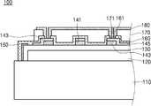
본 발명의 일 실시예에 따른 플렉서블 디스플레이 패널(100)은 플렉서블 기판(120)과 플렉서블 기판(120) 상에 배치된 버퍼층(130)을 포함한다. 버퍼층(130) 상에는 제1 방향(DR1)으로 배열된 복수의 제1 패턴 전극(141)들과, 제1 방향과 교차하는 제2 방향(DR2)으로 배열되며, 제1 패턴 전극(141)들과 절연되도록 이격되어 배치된 복수의 제2 패턴 전극(143)들이 배치된다.The
이 때 버퍼층(130)의 테두리를 따라, 제1 패턴 전극(141)들 및 제2 패턴 전극(143)들과 절연되도록 더미(Dummy) 금속 패턴이 배치된다.At this time, a dummy metal pattern is disposed along the rim of the
또한 버퍼층(130) 상에는 제1 패턴 전극(141)들, 제2 패턴 전극(143)들 및 더미 금속 패턴(150)을 덮도록, 제2 패턴 전극(143)들의 일부가 노출된 복수의 컨택홀을 갖는 산화방지막(160)과 절연층(170)이 배치된다. 산화방지막의 컨택홀(161)과 절연층의 컨택홀(171)을 통해 제2 방향으로 이웃한 제2 전극 패턴들을 전기적으로 연결하는 브릿지 전극(180)들이 배치된다.The
이하에서는 도 2와 도 3을 참고하여 상기의 본 발명의 일 실시예에 따른 플렉서블 디스플레이 패널에 대해서 상세히 설명하도록 한다.Hereinafter, a flexible display panel according to an embodiment of the present invention will be described in detail with reference to FIGS. 2 and 3. FIG.
먼저 글라스 기판과 같은 지지 기판(110) 상에 플렉서블 기판(120)을 배치한다.First, the
플렉서블 디스플레이 패널(100)의 경우 가요성이 있는 플렉서블 기판(120)을 사용하기 때문에, 플렉서블 기판(120) 상에 바로 소자나 다른 층들을 적층하는 공정을 진행하는 경우 기판에 변성이 가해질 수 있다.In the case of the
따라서 본 발명에서는 단단한 판상의 글라스(Glass) 기판을 지지 기판(110)으로 하여, 글라스 기판 상에 플렉서블 기판(120)을 배치하였다. 본 발명의 실시예에서는 글라스 기판을 플렉서블 기판(120) 하부의 지지 기판(110)으로 사용하였지만, 지지 기판(110)은 글라스 기판으로 한정되는 것은 아니다.Therefore, in the present invention, the
이와 같이, 글래스 기판(110)상에 플렉서블 기판(120)을 배치한 후에 공정을 진행하게 되면, 플렉서블 기판(120)에 바로 공정을 진행하는 것과 비교했을 때 플렉서블 기판(120)에 변형이 일어나는 것을 최소화할 수 있다.When the process is performed after the
일반적으로 글라스 기판(110) 상에 플렉서블 기판(120)을 배치한 후에 다수의 후속 공정들을 통해서 플렉서블 디스플레이 패널(100)의 형성이 완료가 되면, 해당 플렉서블 디스플레이 패널(100)을 글라스 기판(110)으로부터 떼어내게 된다.When the
하지만 예를 들어, 터치 디스플레이 패널과 같이 글라스 기판(110)이 디스플레이 패널의 최외면을 형성하는 경우, 상기 공정에서 사용한 글라스 기판(110)을 떼어내지 않고 그대로 디스플레이 패널의 최외면이 되도록 사용할 수도 있다.However, when the
플렉서블 기판(120)은 가요성(Flexibility)이 있는 기판으로, 예를 들어 글라스 기판(110) 상에 투명 폴리이미드(Polyimide) 막을 형성하고 열공정을 수행한 후에 경화를 시켜 형성할 수 있다.The
플렉서블 기판(120)은 폴리에테르술폰(PES, polyethersulphone), 폴리아크릴레이트(PAR, polyacrylate), 폴리에테르 이미드(PEI, polyetherimide), 폴리에틸렌 나프탈레이트(PEN, polyethyelenen napthalate), 폴리에틸렌 테레프탈레이트(PET, polyethyelene terepthalate), 폴리페닐렌 설파이드(PPS, polyphenylene sulfide), 폴리이미드(polyimide), 폴리카보네이트(PC, polycarbonate), 셀룰로오스 트리 아세테이트(TAC, cellulose tri acetate), 셀룰로오스 아세테이트 프로피오네이트(CAP, cellulose acetate propionate) 중 하나 이상을 사용할 수 있으며, 가요성이 있는 기판이라면 특별히 한정되지는 않는다.The
바람직하게는, 플렉서블 기판의 굽힘성(Foldability)과 가요성(Flexibility)의 증대를 위하여, 통상의 뱅크(Bank)나 유기절연막(PAC) 성분으로 사용되는 유기물을 포함하는 기판을 사용할 수 있다.Preferably, a substrate including an organic material used as an ordinary bank or organic insulating film (PAC) component may be used for increasing the foldability and flexibility of the flexible substrate.
예를 들면 뱅크는, 폴리스티렌(Polystylene), 폴리메틸메타아크릴레이트(PMMA), 폴리아크릴로니트릴(PAN), 폴리아미드(Polyamide), 폴리아릴에테르(Polyarylether), 헤테로고리 폴리머(Heterocyclic Polymer), 불소계 고분자, 에폭시 수지(epoxy resin), 벤조사이클로부텐계 수지(benzocyclobuteneseries resin), 실록세인계 수지(siloxane series resin) 및 실란 수지(silane), 아크릴 수지(Acrylic Resin)로 이루어진 군에서 선택되는 하나의 물질 또는 이들의 조합으로 형성될 수 있다.For example, the bank may be made of a material selected from the group consisting of polystyrene, polymethylmethacrylate (PMMA), polyacrylonitrile (PAN), polyamide, polyarylether, heterocyclic polymer, A material selected from the group consisting of a polymer, an epoxy resin, a benzocyclobuteneseries resin, a siloxane series resin and a silane resin, and an acrylic resin. Or a combination thereof.
또한 유기절연막(PAC)은 포토아크릴(Photo-Acryl)과 같은 유기물을 포함할 수 있다.The organic insulating layer (PAC) may include organic materials such as photo-acryl.
플렉서블 기판(120) 상에는 기판 내 수분과 산소의 침투를 방지해주는 역할을 하는 버퍼층(130)이 배치될 수 있다. 버퍼층(130)은 질화실리콘(SiNx) 또는 산화실리콘(SiO2)과 같은 무기물질을 포함할 수 있으며, 단층 또는 다층으로 배치될 수 있다.A
버퍼층(130) 상에는 후술할 금속 재질의 패턴 전극들이 배치될 수 있고, 금속의 경우 유기물보다는 무기물 상에서 더욱 잘 패터닝되기 때문에 버퍼층(130)은 무기물을 포함하거나 무기물만으로 이루어지는 것이 바람직하다.In the case of metal, the
특히 플렉서블 기판(120)이 유기물을 포함하거나 유기물만으로 이루어진 기판인 경우, 무기물을 포함하거나 무기물로만 이루어진 버퍼층(130)을 플렉서블 기판(120) 상에 배치한 후에 후술할 금속 전극 패터닝을 진행하는 것이 바람직하다.In particular, in the case where the
버퍼층(130) 상에는 제1 방향으로 배열된 복수의 제1 패턴 전극(141)들과, 제1 방향과 교차하는 제2 방향으로 배열되며, 제1 패턴 전극(141)들과 절연되도록 이격되어 배치된 복수의 제2 패턴 전극(143)들이 배치된다.A plurality of
제1 패턴 전극(141)들은 복수의 전극선이 교차하여 형성되며 메쉬(Mesh) 형태를 가질 수 있다. 제2 패턴 전극(143)들은 복수의 전극선이 교차하여 형성되며 메쉬(Mesh) 형태를 가질 수 있고, 제1 패턴 전극(141)들과의 교차점에서 연속되지 않고 분리되어 있으며 후술할 브릿지 전극(180)을 통해서 연결된다.The
보다 구체적으로 하나의 제1 패턴 전극(141)은 제1 방향으로는 연결되어 있지만, 복수의 제1 패턴 전극(141)들은 제2 방향으로는 이격되도록 배치되어 있다. 제2 패턴 전극(143)들은 제1 방향과 제2 방향 모두 이격된 섬(Islands) 형태의 서로 분리된 구조를 갖고 있으며, 서로 이웃하는 제2 패턴 전극(143)들은 별도의 전극인 브릿지 전극(180)을 통해서 전기적으로 연결된다.More specifically, the
본 발명의 실시예에서는 제2 패턴 전극(143)들이 불연속적으로 형성된 예를 기준으로 설명하였지만 이에 한정되는 것은 아니다. 즉, 제1 패턴 전극(141)들이 불연속적으로 형성되고, 제2 패턴 전극(143)들이 연속적으로 형성될 수도 있다.In the embodiment of the present invention, the
이러한 금속 전극들의 패턴은 터치 디스플레이 패널에도 적용될 수 있는 바, 본 발명의 실시예에서는 터치 디스플레이 패널에의 적용을 일 실시예로 설명을 하지만 반드시 이에 한정되는 것은 아니다.The pattern of the metal electrodes can be applied to the touch display panel. In the embodiment of the present invention, the application to the touch display panel is described as an embodiment, but it is not limited thereto.
본 발명에 따른 플렉서블 디스플레이 패널이 터치 디스플레이 패널에 적용되는 경우, 서로 교차되는 방향으로 배치된 제1 패턴 전극(141)들과 제2 패턴 전극(143)들은, 터치되는 지점의 X 좌표와 Y 좌표에 대한 정보를 제공한다.When the flexible display panel according to the present invention is applied to a touch display panel, the
구체적으로는 제1 패턴 전극(141) 및 제2 패턴 전극(143)들은 사용자의 터치가 발생하면, 터치의 발생을 감지한다. 이렇게 감지된 신호는 연결 배선(미도시)을 통해 구동회로(미도시) 측으로 접촉위치에 따른 정전용량의 변화가 전달된다. 그리고, X 및 Y 입력처리회로(미도시) 등에 의해 정전용량의 변화가 전기적 신호로 변환되어 접촉위치가 파악된다.Specifically, the
제1 패턴 전극(141) 및 제2 패턴 전극(143)은 금속 전극으로 통상적으로 사용하는 물질이라면 특별히 한정하지 않으나, Cu, Ag, Au, Pt, Al로 이루어진 군에서 선택된 1종 이상의 금속으로 형성될 수 있다.The
또한 제1 패턴 전극(141) 및 제2 패턴 전극(143)은 인듐틴옥사이드(ITO)와 같은 투명 무기산화물로 형성될 수 있으며, ITO 메쉬 형태의 전극 패턴을 형성할 수도 있다.The
추가적으로, 제1 패턴 전극(141)과 제2 패턴 전극(143) 상에는 터치 감도 향상을 위한 별도의 제3 패턴 전극(145)이 배치될 수 있다. 제3 패턴 전극(145)은 인듐틴옥사이드(ITO)와 같은 투명 무기산화물로 형성될 수 있다.In addition, a separate
플렉서블 기판(120) 상에 배치된 버퍼층(130)의 외측 테두리를 따라 더미(Dummy) 금속 패턴(150)이 배치된다. 이 때 더미 금속 패턴(150)은 플렉서블 디스플레이 패널(100) 내의 제1 패턴 전극(141), 제2 패턴 전극(143)들과 같은 다른 금속들과 전기적으로 연결되지 않도록 절연된 상태로 배치가 된다.A
더미 금속 패턴(150)은 플렉서블 디스플레이 패널(100)의 제조 과정에 있어서 다수의 공정을 진행하는 동안 발생될 수 있는 하부의 버퍼층(130) 및 플렉서블 기판(120)의 손상을 최소화해주는 역할을 해준다.The
더미 금속 패턴(150)은 버퍼층(130), 더 나아가서는 플렉서블 기판(120)이 외부로 직접 노출되는 것을 최소화해주기 위하여 버퍼층(130)의 끝단 테두리 부분을 실링(sealing) 하듯이 배치된다.The
이 때 더미 금속 패턴(150)은 제1 패턴 전극(141) 및 제2 패턴 전극(143)이 형성되는 공정과 동시에 형성될 수 있으며, 이러한 경우 더미 금속 패턴(150)은 제1 패턴 전극(141) 및 제2 패턴 전극(143)과 동일한 재질로 형성될 수 있다.At this time, the
또한 더미 금속 패턴(150)은 제3 패턴 전극(145)이 형성되는 동일한 공정에 의해서 형성될 수도 있으며, 이러한 경우 더미 금속 패턴(150)은 제3 패턴 전극(145)과 동일한 재질로 형성될 수 있다.The
이렇게 더미 금속 패턴(150)을 다른 패턴 금속들(141, 143, 145)과 동일한 공정내에서 패터닝하는 것이 가능하기 때문에 더미 금속 패턴(150)의 형성만을 위한 추가 공정이 필요하지 않아 공정 효율이 좋아지고, 비용이 거의 증가되지 않는 장점이 있다.Since it is possible to pattern the
아울러, 더미 금속 패턴(150)은 다른 패턴 금속들(141, 143, 145)과 다른 공정에 의해 다른 물질로 패터닝할 수도 있으며, 이 때의 더미 금속 패턴(150)은 에천트나 기타 오염 물질로부터 영향을 잘 받지 않는 재질인 것이 바람직하다.In addition, the
또한 버퍼층(130) 상에는 제1 패턴 전극(141)들, 제2 패턴 전극(143)들 및 더미 금속 패턴(150)을 덮도록, 제2 패턴 전극(143)들의 일부가 노출된 복수의 컨택홀(161)을 갖는 산화방지막(PAS, 160)이 배치될 수 있다. 제1 패턴 전극(141)들 및 제2 패턴 전극(143)들 상에 제3 패턴 전극(145)이 배치되는 경우에는 제3 패턴 전극(145)을 포함하여 덮도록 산화방지막(160)이 배치될 수 있다.The
산화방지막(160)은 외부 환경에 의한 오염을 방지해주기 위한 것으로, 수분, 산소 등의 침투를 막아 금속을 포함한 하부층들의 손상을 막아주는 역할을 한다. 구체적으로는 실리콘나이트라이드(SiNx), 산화알루미늄(Al2O3), 실리콘 옥사이드(SiO2)들과 같은 무기물들 중에서 하나 이상 선택될 수 있다.The
제2 패턴 전극(143)들 상에 배치된 산화방지막(160)에는 제2 패턴 전극(143)들의 상부면 일부가 노출되도록 컨택홀(161)이 형성될 수 있다.The contact holes 161 may be formed in the
또한 제2 패턴 전극(143)들 상에 제3 패턴 전극(145)이 배치되는 경우에는 제3 패턴 전극(145)들의 상부면 일부가 노출되도록 산화방지막(160)에 컨택홀(161)이 형성될 수 있다.When the
즉, 제1 패턴 전극(141)들과 제2 패턴 전극(143)들의 교차 지점에서 제1 패턴 전극(141)을 중심으로 서로 이웃하는 제2 패턴 전극(143)들 또는 제3 패턴 전극(145)들의 일부가 각각 노출되도록 컨택홀(161)이 형성된다.That is, at the intersection of the
이 컨택홀(161)을 통해 후술할 브릿지 전극(180)은 서로 이웃하는 제2 패턴 전극(143)들 또는 제3 패턴 전극(145)들을 전기적으로 연결시켜주게 된다.A
산화방지막(160)상에는 절연층(PAC, 170)이 추가로 배치될 수 있다. 절연층(170)은 유기물인 포토아크릴(Photo-Acryl)을 포함하는 것이 바람직하다.An insulating layer (PAC) 170 may be additionally disposed on the
절연층(170)은 제1 패턴 전극(141)들과 제2 패턴 전극(143)들을 보호하면서, 제1 패턴 전극(141)들과 제2 패턴 전극(143)들이 서로 간에 전기적으로 절연되도록 해주는 역할을 해준다. 제2 패턴 전극(143)들 상에 제3 패턴 전극(145)이 배치되는 경우에는 제3 패턴 전극(145)들과 제1 패턴 전극(141)들이 절연되도록 해주는 역할도 해준다.The insulating
절연층(170)에는 제1 패턴 전극(141)들과 제2 패턴 전극(143)들의 교차 지점에서 제1 패턴 전극(141)을 중심으로 서로 이웃하는 제2 패턴 전극(143)들의 일부가 각각 노출되도록 절연층의 컨택홀(171)이 형성된다. 절연층(170)의 하부에 산화방지막(160)이 형성된 경우에는 산화방지막의 컨택홀(161)과 절연층의 컨택홀(171)은 서로 연결되도록 형성된다.A portion of the
제2 패턴 전극(143)들 상에 제3 패턴 전극(145)이 배치된 경우에는 절연층의 컨택홀(171)은 제3 패턴 전극(145)의 일부가 노출되도록 형성된다.When the
절연층(170)은 산화방지막(160)의 전면을 덮도록 배치될 수도 있지만, 제1 패턴 전극(141)과 브릿지 전극(180)이 절연되도록 브릿지 전극(180)에만 대응되어 형성될 수 있다.The insulating
아울러 절연층(170)은 산화방지막(160)과 별도의 층으로 형성이 될 수도 있지만, 절연층(170)이 산화방지 역할을 하면서 절연 역할도 할 수 있도록 산화방지막(160)과 일체형으로 형성이 될 수도 있다. 이 경우에는 앞서 설명한 별도의 산화방지막(160)은 형성하지 않고 절연층(170)만 형성하여 산화방지와 절연 효과를 동시에 얻을 수도 있다.The insulating
산화방지막과 절연층이 일체형인 경우, 절연층(170)은 실리콘나이트라이드(SiNx), 산화알루미늄(Al2O3), 실리콘 옥사이드(SiO2)들과 같은 무기물들 중에서 하나 이상 선택되어 사용하는 것이 바람직하다.If the oxide film and the insulating layer is a one-piece, the insulating
브릿지 전극(180)은 산화방지막(160)과 절연층(170)의 컨택홀(161, 171)을 통해 서로 이웃하는 제2 패턴 전극(143)이 제1 패턴 전극(141)과의 교차점에서 전기적으로 연결될 수 있도록 한다. 이 때 제2 패턴 전극(143) 상에 제3 패턴 전극(145)이 형성되어 있는 경우에는 브릿지 전극(180)은 제3 패턴 전극(145)에 연결되도록 형성된다.The
브릿지 전극(180)은 통상적으로 금속 전극으로 사용하는 물질이라면 특별히 한정하지 않으나, Cu, Ag, Au, Pt, Al로 이루어진 군에서 선택된 1종 이상의 금속으로 형성될 수 있다. 바람직하게는 Al/Mo을 사용한다.The
도 4는 플렉서블 디스플레이 패널(100) 제조 공정에 있어서, 산화방지막(160)에 컨택홀을 형성하기 위한 포토리소그래피 공정 단계 중에 있는 플렉서블 디스플레이 패널을 도시한 단면도이다.4 is a cross-sectional view illustrating a flexible display panel in a photolithography process step for forming a contact hole in the
구체적으로, 산화방지막(160) 상에 포토레지스트를 도포하고, 컨택홀 패턴을 가진 마스크를 이용하여 노광(Exposure) 및 현상(Develop) 공정을 거쳐서 포토레지스트 패턴을 형성한 단계를 도시한 것이다.Specifically, a photoresist is coated on the
지지 기판(110) 상에 각 층을 형성하는 경우, 지지 기판(110)의 끝단으로부터 일정 거리의 영역인 이비알(Edge Beads Removal, EBR) 영역을 남겨두고 형성하는 것이 바람직하다.When each layer is formed on the supporting
각 층을 지지 기판(110) 끝단에 맞추어 형성하는 경우 공정 장비에 오염 물질들이 묻어 공정 장비 불량이 발생할 수도 있기 때문에, 이를 최소화하기 위해서 각 층을 형성할 때마다 적정한 거리의 EBR 영역을 형성하게 된다.If each layer is formed at the end of the supporting
이에 따라 기판 EBR 영역(SUB EBR), 버퍼층 EBR 영역(BUF EBR), 산화방지막 EBR 영역(PAS EBR), 포토레지스트 EBR 영역(PR EBR)이 형성된다. 이 때 산화방지막 EBR 영역이 절연층이 산화방지막과 일체형으로 되는 경우에는 절연층 EBR 영역에 대응될 수 있다.Thus, a substrate EBR region (SUB EBR), a buffer layer EBR region (BUF EBR), an oxidation prevention film EBR region (PAS EBR), and a photoresist EBR region (PR EBR) are formed. At this time, the oxidation barrier film EBR region may correspond to the insulation layer EBR region when the insulation layer is integrated with the oxidation barrier film.
각 층의 EBR 영역은 해당 층의 두께를 고려하여 적절히 조절되는 것이 바람직하다. 각 층의 두께에 따라 EBR 영역의 넓이가 달라지기 때문에 각 층에 대응되는 EBR 영역은 차이가 발생할 수 있다.It is preferable that the EBR region of each layer is appropriately adjusted in consideration of the thickness of the layer. Since the width of the EBR region varies depending on the thickness of each layer, a difference in the EBR region corresponding to each layer may occur.
일반적으로 포토레지스트(PR)의 두께는 두껍게 형성되기 때문에, 포토레지스트 EBR은 다른 EBR 영역보다 더욱 넓게 형성이 된다. 이에 따라 산화방지막(160), 버퍼층(130)은 포토레지스트에 의해서 완전히 덮혀지지 않는 영역이 발생할 수 있다.Generally, since the thickness of the photoresist PR is thick, the photoresist EBR is formed wider than the other EBR regions. Accordingly, the
산화방지막(160)의 컨택홀 패턴 형성을 위해서는 드라이 에칭을 실시하게 되는데, 이 때 산화방지막(160)의 컨택홀 패턴에 대응되는 부분뿐만 아니라 포토레지스트에 의해 덮혀지지 않은 산화방지막(160)의 끝단 부분의 일부분까지 에칭의 영향을 받게 된다.Dry etching is performed to form the contact hole pattern of the
이에 따라 산화방지막(160)의 하단부에 있는 버퍼층(130)의 영역과, 더 심한 경우에는 플렉서블 기판(120)의 일부 영역이 외부로 노출될 위험이 생긴다. 하지만 본 발명의 일 실시예에서는 산화방지막(160)의 끝단 테두리 영역의 하단부에 더미 금속 패턴(150)이 배치되어 있어, 더미 금속 패턴(150)은 에칭으로부터 해당 영역이 외부로 노출되는 것을 최소화하고 보호해주는 역할을 해준다.Thereby, there is a risk that the area of the
또한 후속 공정으로 브릿지 전극(180)을 형성하는 과정에서, 에천트를 사용하는 웨트 에칭 공정이 진행될 수 있다. 이 때 사용되는 에천트가 외부로 노출된 플렉서블 기판(120)의 하부면으로 스며들게 되는 경우 글라스 기판(110)과 플렉서블 기판(120)이 필링(Peeling)되는 현상이 발생할 수도 있다. 하지만 본 발명에서는 더미 금속 패턴(150)이 보호 역할을 해주어 이러한 현상의 발생을 최소화시킬 수 있다.Further, in the process of forming the
즉, 더미 금속 패턴(150)의 배치로 인해 버퍼층(130)과 플렉서블 기판(120)의 외부 노출을 최소화시켜 플렉서블 기판(120)과 글라스 기판(110) 사이에 발생할 수 있는 필링(Peeling)의 문제를 최소화시켜줄 수 있다. 이를 통해 플렉서블 기판(120)의 손상과 이로 인한 플렉서블 디스플레이 패널(100)의 불량을 최소화할 수 있다.That is, since the external exposure of the
특히 굽힘성과 가요성이 더욱 높은 유기물 성분의 플렉서블 기판(120)을 사용하는 경우에 더미 금속 패턴(150)의 배치는 더욱 큰 효과를 얻을 수 있다. 이는 유기물 성분의 플렉서블 기판(120)은 에천트와 같은 외부 요인에 더욱 취약하기 때문에 더미 금속 패턴(150)의 배치로 인한 더 큰 보호 효과를 얻을 수 있기 때문이다.Particularly, when the
도 5는 도 3에 의한 본 발명의 실시예에 따른 플렉서블 디스플레이 패널 제조 방법에 대한 공정도이다.FIG. 5 is a process diagram of a method of manufacturing a flexible display panel according to an embodiment of the present invention with reference to FIG.
본 제조 방법에 따르면, 지지 기판(110) 상에 플렉서블 기판(120)을 형성하는 단계(S11), 플렉서블 기판(120) 상에 버퍼층(130)을 형성하는 단계(S12), 버퍼층(130) 상에 제1 패턴 전극(141), 제2 패턴 전극(143), 더미 금속 패턴(150)을 동시에 형성하는 단계(S13), 절연층(170)을 형성하는 단계(S14), 브릿지 전극(180)을 형성하여 서로 이웃하는 제2 패턴 전극(143)끼리 연결하는 단계(S15)를 포함한다.According to the present manufacturing method, a
S14 단계에 있어서, 절연층(170)을 형성하기 전에 산화방지막(160)을 추가적으로 형성할 수도 있다.In step S14, the
구체적으로는 지지 기판(110) 상에 플렉서블 기판(120)을 먼저 형성하고, 플렉서블 기판(120) 상에 버퍼층(130)을 형성한다.More specifically, the
이후 버퍼층(130) 상에 복수의 제1 패턴 전극(141)들을 제1 방향으로 배열하여 형성하고, 복수의 제2 패턴 전극(143)들을 상기 제1 방향과 교차하는 제2 방향으로 배열하고 상기 제1 패턴 전극(141)들과 절연되도록 이격하여 형성한다. 또한 제1 패턴 전극(141)들 및 제2 패턴 전극(143)들을 형성하는 동일한 공정 내에서, 더미 금속 패턴(150)을 제1 패턴 전극(141)들 및 제2 패턴 전극(143)들과 동시에 형성한다. 이 때 더미 금속 패턴(150)은 버퍼층(130)의 테두리를 따라 제1 패턴 전극(141)들 및 제2 패턴 전극(143)들과 절연되도록 배치한다.A plurality of
이후 제1 패턴 전극(141)들, 제2 패턴 전극(143)들 및 더미 금속 패턴(150)을 덮도록 산화방지막(160)과 절연층(170)을 형성하고 각각의 컨택홀(161, 171)을 형성한다.The
절연층(170) 상에 브릿지 전극(180)을 형성하여 서로 이웃하는 제2 패턴 전극(143)을 전기적으로 연결시킨다.A
본 발명에 따른 제조 방법은, S13 단계와 같이 더미 금속 패턴(150)을 제1 패턴 전극(141), 제2 패턴 전극(143)과 동시에 형성하게 되는 바, 더미 금속 패턴(150)의 형성을 위한 공정의 추가가 필요하지 않아 높은 공정의 효율성과 비용의 절감 효과를 얻을 수 있다.The
각 단계에서 각 층들을 형성하는 방법은 플렉서블 터치 디스플레이 패널을 제조하는 통상의 알려진 다양한 방법들을 사용할 수 있는 바 자세한 설명은 생략하도록 한다.As a method of forming each layer in each step, various known methods for manufacturing a flexible touch display panel can be used, and a detailed description will be omitted.
예를 들어, 반응성 스퍼터링(Reactive Sputtering)과 같은 물리적 증착(Physical Vapor Deposition, PVD), 화학적 증착(Chemical Vapor Deposition, CVD)등 다양한 박막 증착 기술에 의해 형성될 수 있다. 이외에도 각 층은 포토리소그래피 공정 등에 의해서 형성될 수도 있다.For example, by various thin film deposition techniques such as physical vapor deposition (PVD) such as reactive sputtering, chemical vapor deposition (CVD), and the like. In addition, each layer may be formed by a photolithography process or the like.
또한, 금속 패턴은 그라비아 오프 셋(Gravure off set), 리버스 오프 셋(Reverse off set), 잉크젯 인쇄, 스크린 인쇄 및 그라비아(Gravure) 인쇄 등과 같은 다양한 인쇄 공정으로 형성될 수도 있다.In addition, the metal pattern may be formed by various printing processes such as gravure off set, reverse off set, ink jet printing, screen printing and gravure printing.
도 6은 본 발명의 다른 일 실시예에 따른 플렉서블 디스플레이 패널에 대한 단면도이다.6 is a cross-sectional view of a flexible display panel according to another embodiment of the present invention.
본 발명의 다른 일 실시예에 따른 플렉서블 디스플레이 패널(100)은 플렉서블 기판(120)과 플렉서블 기판(120)의 테두리를 따라 배치된 더미 금속 패턴(150)을 포함한다.The
플렉서블 기판(120) 상에는 더미 금속 패턴(150)을 덮도록 버퍼층(130)이 배치된다. 버퍼층(130) 상에는 제1 방향으로 배열된 복수의 제1 패턴 전극(141)들과, 제1 방향과 교차하는 제2 방향으로 배열되며, 제1 패턴 전극(141)들과 절연되도록 이격되어 배치된 복수의 제2 패턴 전극(143)들이 배치된다.A
또한 버퍼층(130) 상에는 제1 패턴 전극(141)들, 제2 패턴 전극(143)들을 덮도록, 제2 패턴 전극(143)들의 일부가 노출된 복수의 컨택홀을 갖는 산화방지막(160)과 절연층(170)이 배치된다. 산화방지막의 컨택홀(161)과 절연층의 컨택홀(171)을 통해 제2 방향으로 이웃한 제2 전극 패턴들을 전기적으로 연결하는 브릿지 전극(180)들이 배치된다.An
도 6에 의한 실시예의 경우 버퍼층(130)의 테두리가 아닌 플렉서블 기판(120)의 테두리에 더미 금속 패턴(150)이 배치되는 점에서 도 3에 의한 실시예와 차이가 있다. 즉, 도 6에 의한 실시예의 경우 플렉서블 기판(120) 상에 바로 더미 금속 패턴(150)이 배치되어 플렉서블 기판(120)의 손상을 방지해주는 역할을 한다.6 differs from the embodiment shown in FIG. 3 in that the
따라서 앞서 설명한 공정들을 통해서, 더미 금속 패턴(150)상에 배치된 버퍼층(130)의 일부 영역이 에칭된다고 하더라도 더미 금속 패턴(150)이 하부의 플렉서블 기판(120)을 보호해주는 역할을 해 줄 수 있다.Therefore, even if a portion of the
이외 생략된 설명들의 경우 도 3을 통해서 설명된 실시예와 동일하게 적용이 가능한 바 중복되는 내용들은 추가 설명을 하지 않도록 한다.In the case of the other explanations, the same description can be applied to the embodiment explained in FIG. 3, but the redundant contents are not explained further.
도 7은 본 발명의 또 다른 일 실시예에 따른 플렉서블 디스플레이 패널에 대한 단면도이다.7 is a cross-sectional view of a flexible display panel according to another embodiment of the present invention.
본 발명은 앞서 설명한 도 3과 도 6에서 설명된 실시예와 달리 브릿지 전극(280)이 제1 패턴 전극(241)들과 제2 패턴 전극(243)들의 하부면에 배치된 실시예에 대한 것이다.The present invention is directed to an embodiment in which the
본 발명의 일 실시예에 따른 플렉서블 디스플레이 패널(200)은 플렉서블 기판(220)과 플렉서블 기판(220) 상에 배치된 버퍼층(230)을 포함한다. 버퍼층(230) 상에는 복수의 브릿지 전극(280)들이 배치되고, 버퍼층(230)의 테두리에는 더미 금속 패턴(250)이 브릿지 전극(280)들과 절연되도록 배치된다.The
또한 브릿지 전극(280)들과 더미 금속 패턴(250)을 덮도록, 브릿지 전극(280)들의 일부가 노출된 복수의 컨택홀(261, 271)을 갖는 산화방지막(260)과 절연층(270)이 버퍼층(230) 상에 배치된다. 절연층(270) 상에는 제1 방향으로 배열된 복수의 제1 패턴 전극(241)들, 제1 방향과 교차하는 제2 방향으로 배열되고, 상기 제1 패턴 전극(241)들과 절연되도록 이격되어 배치된 복수의 제2 패턴 전극(243)들이 배치된다.An
이 때 제2 방향으로 이웃한 제2 전극 패턴들은 산화방지막(260)과 절연층(270)의 컨택홀(261, 271)을 통해 브릿지 전극(280)들에 의해 전기적으로 연결된다.At this time, the second electrode patterns neighboring in the second direction are electrically connected by the
도 7에 의한 실시예의 경우 도 3 또는 도 6에 의한 실시예와 동일하게, 버퍼층(230)의 외측 테두리에 더미 금속 패턴(250)이 배치되어 하부의 버퍼층(230)과 플렉서블 기판(220)의 손상을 최소화시켜줄 수 있다.7, a
이 때 더미 금속 패턴(150)은 브릿지 전극(280)이 형성되는 공정과 동시에 형성될 수 있으며, 이러한 경우 더미 금속 패턴(150)은 브릿지 전극(280)과 동일한 재질로 형성될 수 있다.At this time, the
이렇게 더미 금속 패턴(150)을 브릿지 전극(280)과 동일한 공정내에서 패터닝하는 것이 가능하기 때문에 더미 금속 패턴(150)의 형성만을 위한 추가 공정이 필요하지 않아 공정 효율이 좋아지고, 비용이 거의 증가되지 않는 장점이 있다.Since the
이외 생략된 설명들의 경우 도 3 및 도 6을 통해서 설명된 실시예와 동일하게 적용이 가능한 바 중복되는 내용들은 추가 설명을 하지 않도록 한다.In the case of other explanations, the same description can be applied to the embodiments described with reference to FIG. 3 and FIG. 6, but redundant descriptions are not described further.
도 8은 도 7에 의한 본 발명의 또 다른 실시예에 따른 플렉서블 디스플레이 패널 제조 방법에 대한 공정도이다.FIG. 8 is a process diagram of a method of manufacturing a flexible display panel according to another embodiment of the present invention. Referring to FIG.
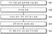
본 제조 방법에 따르면, 지지 기판(210) 상에 플렉서블 기판(220)을 형성하는 단계(S21), 플렉서블 기판(220) 상에 버퍼층(230)을 형성하는 단계(S22), 버퍼층(230) 상에 브릿지 전극(280)과 더미 금속 패턴(250)을 동시에 형성하는 단계(S23), 절연층(270)을 형성하는 단계(S24), 제1 패턴 전극(241), 제2 패턴 전극(243)을 형성하고 제2 패턴 전극(243)을 브릿지 전극(280)과 연결하는 단계(S25)를 포함한다.According to the present manufacturing method, a
S24 단계에 있어서, 절연층(270)을 형성하기 전에 산화방지막(260)을 추가적으로 형성할 수도 있다.In step S24, the
구체적으로는 지지 기판(210) 상에 플렉서블 기판(220)을 형성하고, 플렉서블 기판(220) 상에 버퍼층(230)을 형성한다.More specifically, the
버퍼층(230) 상에 복수의 브릿지 전극(280)들을 형성하고, 브릿지 전극(280)을 형성하는 동일한 공정 내에서 더미 금속 패턴(250)을 브릿지 전극(280)들과 동시에 형성한다. 이 때 더미 금속 패턴(250)은 버퍼층(230)의 테두리를 따라 브릿지 전극(280)들과 절연되도록 배치한다.A plurality of
이후에 브릿지 전극(280)들 및 더미 금속 패턴(250)을 덮도록 산화방지막(260)과 절연층(270)을 형성하고, 각각의 컨택홀(261, 271)을 형성한다.The
이후에 절연층 상에 복수의 제1 패턴 전극(241)들을 제1 방향으로 배열되도록 형성한다. 또한 복수의 제2 패턴 전극(243)들을 제1 방향과 교차하는 제2 방향으로 배열하고 제1 패턴 전극(241)들과 절연되도록 이격하여 형성하며, 서로 이웃하는 제2 패턴 전극(243)들을 브릿지 전극(280)과 전기적으로 연결시키는 단계를 포함한다.Then, a plurality of
본 발명에 따른 제조 방법은, S23 단계와 같이 더미 금속 패턴(250)을 브릿지 전극(280)과 동시에 형성하게 되는 바, 더미 금속 패턴(250)의 형성을 위한 공정의 추가가 필요하지 않아 높은 공정의 효율성과 비용의 절감 효과를 얻을 수 있다.Since the
각 단계에서 각 층들을 형성하는 방법은 플렉서블 터치 디스플레이 패널을 제조하는 통상의 알려진 다양한 방법들을 사용할 수 있는 바 자세한 설명은 생략하도록 한다.As a method of forming each layer in each step, various known methods for manufacturing a flexible touch display panel can be used, and a detailed description will be omitted.
예를 들어, 반응성 스퍼터링(Reactive Sputtering)과 같은 물리적 증착(Physical Vapor Deposition, PVD), 화학적 증착(Chemical Vapor Deposition, CVD)등 다양한 박막 증착 기술에 의해 형성될 수 있다. 이외에도 각 층은 포토리소그래피 공정 등에 의해서 형성될 수도 있다.For example, by various thin film deposition techniques such as physical vapor deposition (PVD) such as reactive sputtering, chemical vapor deposition (CVD), and the like. In addition, each layer may be formed by a photolithography process or the like.
또한, 금속 패턴은 그라비아 오프 셋(Gravure off set), 리버스 오프 셋(Reverse off set), 잉크젯 인쇄, 스크린 인쇄 및 그라비아(Gravure) 인쇄 등과 같은 다양한 인쇄 공정으로 형성될 수도 있다.In addition, the metal pattern may be formed by various printing processes such as gravure off set, reverse off set, ink jet printing, screen printing and gravure printing.
도 9는 본 발명의 또 다른 실시예에 대한 단면도이다.9 is a cross-sectional view of another embodiment of the present invention.
본 발명의 또 다른 실시예에 따른 플렉서블 디스플레이 패널(200)은 플렉서블 기판(220)과 플렉서블 기판(220)의 테두리를 따라 배치된 더미 금속 패턴(250)을 포함한다. 플렉서블 기판(220) 상에는 더미 금속 패턴(250)을 덮도록 버퍼층(230)이 배치되며, 버퍼층(230) 상에는 복수의 브릿지 전극(280)들이 배치된다.The
또한 브릿지 전극(280)들을 덮도록, 브릿지 전극(280)들의 일부가 노출된 복수의 컨택홀을 갖는 산화방지막(260)과 절연층(270)이 버퍼층(230) 상에 배치된다. 절연층(270) 상에는 제1 방향으로 배열된 복수의 제1 패턴 전극(241)들, 제1 방향과 교차하는 제2 방향으로 배열되고, 상기 제1 패턴 전극(241)들과 절연되도록 이격되어 배치된 복수의 제2 패턴 전극(243)들이 배치된다.The
이 때 제2 방향으로 이웃한 제2 전극 패턴(243)들은 산화방지막(260)과 절연층(270)의 컨택홀(261, 271)을 통해 브릿지 전극(280)들에 의해 전기적으로 연결된다.At this time, the
도 9에 의한 실시예의 경우 플렉서블 기판(220)의 테두리에 더미 금속 패턴(250)이 배치되는 점에서 도 8에 의한 실시예와 차이가 있다. 즉, 도 9에 의한 실시예의 경우 플렉서블 기판(220) 상에 바로 더미 금속 패턴(250)이 배치되어 플렉서블 기판(220)의 손상을 방지해주는 역할을 한다.9 differs from the embodiment shown in FIG. 8 in that the
이외 생략된 설명들의 경우 앞서 설명된 실시예들과 동일하게 적용이 가능한 바 중복되는 내용들은 추가 설명을 하지 않도록 한다.In the case of the other explanations, it is possible to apply the same to the embodiments described above.
이상에서는 본 발명의 실시예를 중심으로 설명하였지만, 통상의 기술자의 수준에서 다양한 변경이나 변형을 가할 수 있다. 따라서, 이러한 변경과 변형이 본 발명의 범위를 벗어나지 않는 한 본 발명의 범주 내에 포함되는 것으로 이해될 수 있을 것이다.While the present invention has been particularly shown and described with reference to exemplary embodiments, it is to be understood that the invention is not limited to the disclosed exemplary embodiments. It is therefore to be understood that such changes and modifications are intended to be included within the scope of the present invention unless they depart from the scope of the present invention.
1 : 플렉서블 디스플레이 패널10 : 지지 기판
20 : 플렉서블 기판41 : 제1 패턴 전극
43 : 제2 패턴 전극70 : 절연층
71 : 절연층의 컨택홀80 : 브릿지 전극
100, 200 : 플렉서블 디스플레이 패널110, 210 : 지지 기판
120, 220 : 플렉서블 기판130, 230 : 버퍼층
141, 241 : 제1 패턴 전극143, 243 : 제2 패턴 전극
145 : 제3 패턴 전극150, 250 : 더미 금속 패턴
160, 260 : 산화방지막161, 261 : 산화방지막의 컨택홀
170, 270 : 절연층171, 271 : 절연층의 컨택홀
180, 280 : 브릿지 전극1: Flexible display panel 10: Support substrate
20: flexible substrate 41: first pattern electrode
43: second pattern electrode 70: insulating layer
71: contact hole of insulating layer 80: bridge electrode
100, 200:
120, 220:
141, 241:
145:
160, 260:
170, 270: insulating
180, 280: bridge electrode
Claims (14)
Translated fromKorean상기 플렉서블 기판 상에 배치된 버퍼층;
상기 버퍼층 상에 제1 방향으로 배열된 복수의 제1 패턴 전극들;
상기 버퍼층 상에 상기 제1 방향과 교차하는 제2 방향으로 배열되며, 상기 제1 패턴 전극들과 절연되도록 이격되어 배치된 복수의 제2 패턴 전극들;
상기 버퍼층의 테두리를 따라 배치되고, 상기 제1 패턴 전극들 및 상기 제2 패턴 전극들과 절연된 더미 금속 패턴;
상기 제1 패턴 전극들, 상기 제2 패턴 전극들 및 상기 더미 금속 패턴을 덮도록 상기 버퍼층 상에 배치되고, 상기 제2 패턴 전극들의 일부가 노출된 복수의 컨택홀을 갖는 절연층; 및
상기 컨택홀을 통해 상기 제2 방향으로 이웃한 제2 전극 패턴들을 전기적으로 연결한 복수의 브릿지 전극들; 을 포함하는 플렉서블 디스플레이 패널.
A flexible substrate;
A buffer layer disposed on the flexible substrate;
A plurality of first pattern electrodes arranged in a first direction on the buffer layer;
A plurality of second pattern electrodes arranged on the buffer layer in a second direction intersecting the first direction and spaced apart from the first pattern electrodes so as to be insulated from the first pattern electrodes;
A dummy metal pattern disposed along the rim of the buffer layer and insulated from the first pattern electrodes and the second pattern electrodes;
An insulating layer disposed on the buffer layer so as to cover the first pattern electrodes, the second pattern electrodes, and the dummy metal pattern, the insulating layer having a plurality of contact holes in which a part of the second pattern electrodes is exposed; And
A plurality of bridge electrodes electrically connecting the second electrode patterns neighboring in the second direction through the contact holes; And a flexible display panel.
상기 플렉서블 기판의 테두리를 따라 배치된 더미 금속 패턴;
상기 더미 금속 패턴을 덮도록 상기 플렉서블 기판 상에 배치된 버퍼층;
상기 버퍼층 상에 제1 방향으로 배열된 복수의 제1 패턴 전극들;
상기 버퍼층 상에 상기 제1 방향과 교차하는 제2 방향으로 배열되며, 상기 제1 패턴 전극들과 절연되도록 이격되어 배치된 복수의 제2 패턴 전극들;
상기 제1 패턴 전극들과 상기 제2 패턴 전극들을 덮도록 상기 버퍼층 상에 배치되고, 상기 제2 패턴 전극들의 일부가 노출된 복수의 컨택홀을 갖는 절연층; 및
상기 컨택홀을 통해 상기 제2 방향으로 이웃한 제2 전극 패턴들을 전기적으로 연결한 복수의 브릿지 전극들; 을 포함하는 플렉서블 디스플레이 패널.
A flexible substrate;
A dummy metal pattern disposed along the rim of the flexible substrate;
A buffer layer disposed on the flexible substrate so as to cover the dummy metal pattern;
A plurality of first pattern electrodes arranged in a first direction on the buffer layer;
A plurality of second pattern electrodes arranged on the buffer layer in a second direction intersecting the first direction and spaced apart from the first pattern electrodes so as to be insulated from the first pattern electrodes;
An insulating layer disposed on the buffer layer so as to cover the first pattern electrodes and the second pattern electrodes and having a plurality of contact holes in which a part of the second pattern electrodes is exposed; And
A plurality of bridge electrodes electrically connecting the second electrode patterns neighboring in the second direction through the contact holes; And a flexible display panel.
상기 플렉서블 기판은 유기물을 포함하고, 상기 버퍼층은 무기물을 포함하는, 플렉서블 디스플레이 패널.
3. The method according to claim 1 or 2,
Wherein the flexible substrate comprises an organic material, and the buffer layer comprises an inorganic material.
상기 더미 금속 패턴은 상기 제1 패턴 전극들 및 상기 제2 패턴 전극들과 동일한 재질인, 플렉서블 디스플레이 패널.
The method according to claim 1,
Wherein the dummy metal pattern is made of the same material as the first pattern electrodes and the second pattern electrodes.
상기 버퍼층과 상기 절연층 사이에는 산화방지막이 추가로 배치된, 플렉서블 디스플레이 패널.
3. The method according to claim 1 or 2,
And an oxidation preventing film is further disposed between the buffer layer and the insulating layer.
상기 제1 패턴 전극 및 제2 패턴 전극 상에는 제3 패턴 전극이 추가로 배치된, 플렉서블 디스플레이 패널.
3. The method according to claim 1 or 2,
And a third pattern electrode is further disposed on the first pattern electrode and the second pattern electrode.
상기 더미 금속 패턴은 상기 제3 패턴 전극과 동일한 재질인, 플렉서블 디스플레이 패널.
The method according to claim 6,
Wherein the dummy metal pattern is made of the same material as the third pattern electrode.
상기 플렉서블 기판 상에 배치된 버퍼층;
상기 버퍼층 상에 배치된 복수의 브릿지 전극들;
상기 버퍼층의 테두리를 따라 배치되고, 상기 브릿지 전극들과 절연된 더미 금속 패턴;
상기 브릿지 전극들과 상기 더미 금속 패턴을 덮도록 상기 버퍼층 상에 배치되고, 상기 브릿지 전극들의 일부가 노출된 복수의 컨택홀을 갖는 절연층;
상기 절연층 상에 제1 방향으로 배열된 복수의 제1 패턴 전극들;
상기 절연층 상에 상기 제1 방향과 교차하는 제2 방향으로 배열되고, 상기 제1 패턴 전극들과 절연되도록 이격되어 배치된 복수의 제2 패턴 전극들; 및
상기 제2 방향으로 이웃한 제2 전극 패턴들은 상기 절연층의 컨택홀을 통해 상기 브릿지 전극들에 의해 전기적으로 연결된 플렉서블 디스플레이 패널.
A flexible substrate;
A buffer layer disposed on the flexible substrate;
A plurality of bridge electrodes disposed on the buffer layer;
A dummy metal pattern disposed along the rim of the buffer layer and insulated from the bridge electrodes;
An insulating layer disposed on the buffer layer to cover the bridge electrodes and the dummy metal pattern, the insulating layer having a plurality of contact holes in which a part of the bridge electrodes are exposed;
A plurality of first pattern electrodes arranged in a first direction on the insulating layer;
A plurality of second pattern electrodes arranged on the insulating layer in a second direction intersecting with the first direction and arranged so as to be insulated from the first pattern electrodes; And
And the second electrode patterns neighboring in the second direction are electrically connected by the bridge electrodes through the contact holes of the insulating layer.
상기 플렉서블 기판의 테두리를 따라 배치된 더미 금속 패턴;
상기 더미 금속 패턴을 덮도록 상기 플렉서블 기판 상에 배치된 버퍼층;
상기 버퍼층 상에 배치된 복수의 브릿지 전극들;
상기 브릿지 전극들을 덮도록 상기 버퍼층 상에 배치되고, 상기 브릿지 전극들의 일부가 노출된 복수의 컨택홀을 갖는 절연층;
상기 절연층 상에 제1 방향으로 배열된 복수의 제1 패턴 전극들;
상기 절연층 상에 상기 제1 방향과 교차하는 제2 방향으로 배열되고, 상기 제1 패턴 전극들과 절연되도록 이격되어 배치된 복수의 제2 패턴 전극들; 및
상기 제2 방향으로 이웃한 제2 전극 패턴들은 상기 절연층의 컨택홀을 통해 상기 브릿지 전극들에 의해 전기적으로 연결된 플렉서블 디스플레이 패널.
A flexible substrate;
A dummy metal pattern disposed along the rim of the flexible substrate;
A buffer layer disposed on the flexible substrate so as to cover the dummy metal pattern;
A plurality of bridge electrodes disposed on the buffer layer;
An insulating layer disposed on the buffer layer to cover the bridge electrodes, the insulating layer having a plurality of contact holes in which a part of the bridge electrodes are exposed;
A plurality of first pattern electrodes arranged in a first direction on the insulating layer;
A plurality of second pattern electrodes arranged on the insulating layer in a second direction intersecting with the first direction and arranged so as to be insulated from the first pattern electrodes; And
And the second electrode patterns neighboring in the second direction are electrically connected by the bridge electrodes through the contact holes of the insulating layer.
상기 플렉서블 기판은 유기물을 포함하고, 상기 버퍼층은 무기물을 포함하는, 플렉서블 디스플레이 패널.
10. The method according to claim 8 or 9,
Wherein the flexible substrate comprises an organic material, and the buffer layer comprises an inorganic material.
상기 더미 금속 패턴과 상기 브릿지 전극들은 동일한 재질인, 플렉서블 디스플레이 패널.
9. The method of claim 8,
Wherein the dummy metal pattern and the bridge electrodes are made of the same material.
상기 버퍼층과 상기 절연층 사이에는 산화방지막이 추가로 배치된, 플렉서블 디스플레이 패널.
10. The method according to claim 8 or 9,
And an oxidation preventing film is further disposed between the buffer layer and the insulating layer.
상기 플렉서블 기판 상에 버퍼층을 형성하는 단계;
상기 버퍼층 상에 복수의 제1 패턴 전극들을 제1 방향으로 배열하고,
복수의 제2 패턴 전극들을 상기 제1 패턴 전극들과 절연되도록 이격하여상기 제1 방향과 교차하는 제2 방향으로 배열하며,
상기 버퍼층의 테두리를 따라 더미 금속 패턴을 상기 제1 패턴 전극들 및 상기 제2 패턴 전극들과 절연되도록 배치하되,
상기 더미 금속 패턴을 상기 제1 패턴 전극들 및 상기 제2 패턴 전극들과 동시에 형성하는 단계;
상기 제1 패턴 전극들, 상기 제2 패턴 전극들 및 상기 더미 금속 패턴을 덮도록 절연층과 상기 절연층의 컨택홀을 형성하는 단계; 및
상기 절연층 상에 브릿지 전극을 형성하여 서로 이웃하는 상기 제2 패턴 전극들을 전기적으로 연결시키는 단계; 를 포함하는 플렉서블 디스플레이 패널 제조 방법.
Forming a flexible substrate on the supporting substrate;
Forming a buffer layer on the flexible substrate;
Arranging a plurality of first pattern electrodes on the buffer layer in a first direction,
A plurality of second pattern electrodes arranged in a second direction so as to be insulated from the first pattern electrodes and intersecting the first direction,
A dummy metal pattern is disposed along the rim of the buffer layer so as to be insulated from the first pattern electrodes and the second pattern electrodes,
Forming the dummy metal pattern simultaneously with the first pattern electrodes and the second pattern electrodes;
Forming an insulation layer and a contact hole of the insulation layer so as to cover the first pattern electrodes, the second pattern electrodes, and the dummy metal pattern; And
Forming a bridge electrode on the insulating layer and electrically connecting neighboring second pattern electrodes; Wherein the flexible display panel comprises a flexible substrate.
상기 플렉서블 기판 상에 버퍼층을 형성하는 단계;
상기 버퍼층 상에 복수의 브릿지 전극들을 배치하고,
상기 버퍼층의 테두리를 따라 더미 금속 패턴을 상기 브릿지 전극들과 절연되도록 배치하되,
상기 더미 금속 패턴을 상기 브릿지 전극들과 동시에 형성하는 단계;
상기 브릿지 전극들 및 더미 금속 패턴을 덮도록 절연층과 상기 절연층의 컨택홀을 형성하는 단계; 및
상기 절연층 상에 복수의 제1 패턴 전극들을 제1 방향으로 배열하고,
복수의 제2 패턴 전극들을 상기 제1 패턴 전극들과 절연되도록 이격하여 상기 제1 방향과 교차하는 제2 방향으로 배열하며,
서로 이웃하는 상기 제2 패턴 전극들을 상기 브릿지 전극들과 전기적으로 연결시키는 단계; 를 포함하는 플렉서블 디스플레이 패널 제조 방법.Forming a flexible substrate on the supporting substrate;
Forming a buffer layer on the flexible substrate;
Arranging a plurality of bridge electrodes on the buffer layer,
A dummy metal pattern is disposed along the rim of the buffer layer so as to be insulated from the bridge electrodes,
Forming the dummy metal pattern simultaneously with the bridge electrodes;
Forming an insulation layer and a contact hole of the insulation layer so as to cover the bridge electrodes and the dummy metal pattern; And
Arranging a plurality of first pattern electrodes on the insulating layer in a first direction,
A plurality of second pattern electrodes arranged in a second direction so as to be insulated from the first pattern electrodes and intersecting the first direction,
Electrically connecting the second pattern electrodes adjacent to each other to the bridge electrodes; Wherein the flexible display panel comprises a flexible substrate.
Priority Applications (1)
| Application Number | Priority Date | Filing Date | Title |
|---|---|---|---|
| KR1020160055724AKR102512040B1 (en) | 2016-05-04 | 2016-05-04 | Flexible display panel and manufacturing method of thereof |
Applications Claiming Priority (1)
| Application Number | Priority Date | Filing Date | Title |
|---|---|---|---|
| KR1020160055724AKR102512040B1 (en) | 2016-05-04 | 2016-05-04 | Flexible display panel and manufacturing method of thereof |
Publications (2)
| Publication Number | Publication Date |
|---|---|
| KR20170125638Atrue KR20170125638A (en) | 2017-11-15 |
| KR102512040B1 KR102512040B1 (en) | 2023-03-20 |
Family
ID=60387158
Family Applications (1)
| Application Number | Title | Priority Date | Filing Date |
|---|---|---|---|
| KR1020160055724AActiveKR102512040B1 (en) | 2016-05-04 | 2016-05-04 | Flexible display panel and manufacturing method of thereof |
Country Status (1)
| Country | Link |
|---|---|
| KR (1) | KR102512040B1 (en) |
Cited By (3)
| Publication number | Priority date | Publication date | Assignee | Title |
|---|---|---|---|---|
| CN109326565A (en)* | 2018-07-06 | 2019-02-12 | 友达光电股份有限公司 | Flexible panel and method of making the same |
| KR20210081665A (en)* | 2019-12-24 | 2021-07-02 | 동우 화인켐 주식회사 | Touch sensor and image display device including the same |
| CN113362707A (en)* | 2020-03-04 | 2021-09-07 | 三星显示有限公司 | Display device and method for manufacturing the same |
Citations (6)
| Publication number | Priority date | Publication date | Assignee | Title |
|---|---|---|---|---|
| KR20110095669A (en)* | 2010-02-19 | 2011-08-25 | (주)삼원에스티 | Touch Panel Sensor with Low Resistance Line |
| KR20120106526A (en)* | 2011-03-18 | 2012-09-26 | 티피케이 터치 솔루션즈 (씨아먼) 인코포레이티드 | Touch device and fabrication method thereof |
| WO2015008642A1 (en)* | 2013-07-16 | 2015-01-22 | シャープ株式会社 | Method for producing flexible display device, and flexible display device |
| KR20150062638A (en)* | 2013-11-29 | 2015-06-08 | 삼성디스플레이 주식회사 | Method of fabricating flexible display device |
| JP2015180930A (en)* | 2014-03-06 | 2015-10-15 | 株式会社半導体エネルギー研究所 | light-emitting device |
| KR20160043697A (en)* | 2014-10-14 | 2016-04-22 | 엘지디스플레이 주식회사 | Touch panel and touch panel integrated organic light emitting display device |
- 2016
- 2016-05-04KRKR1020160055724Apatent/KR102512040B1/enactiveActive
Patent Citations (6)
| Publication number | Priority date | Publication date | Assignee | Title |
|---|---|---|---|---|
| KR20110095669A (en)* | 2010-02-19 | 2011-08-25 | (주)삼원에스티 | Touch Panel Sensor with Low Resistance Line |
| KR20120106526A (en)* | 2011-03-18 | 2012-09-26 | 티피케이 터치 솔루션즈 (씨아먼) 인코포레이티드 | Touch device and fabrication method thereof |
| WO2015008642A1 (en)* | 2013-07-16 | 2015-01-22 | シャープ株式会社 | Method for producing flexible display device, and flexible display device |
| KR20150062638A (en)* | 2013-11-29 | 2015-06-08 | 삼성디스플레이 주식회사 | Method of fabricating flexible display device |
| JP2015180930A (en)* | 2014-03-06 | 2015-10-15 | 株式会社半導体エネルギー研究所 | light-emitting device |
| KR20160043697A (en)* | 2014-10-14 | 2016-04-22 | 엘지디스플레이 주식회사 | Touch panel and touch panel integrated organic light emitting display device |
Cited By (4)
| Publication number | Priority date | Publication date | Assignee | Title |
|---|---|---|---|---|
| CN109326565A (en)* | 2018-07-06 | 2019-02-12 | 友达光电股份有限公司 | Flexible panel and method of making the same |
| TWI684266B (en)* | 2018-07-06 | 2020-02-01 | 友達光電股份有限公司 | Flexible panel and method of fabricating the same |
| KR20210081665A (en)* | 2019-12-24 | 2021-07-02 | 동우 화인켐 주식회사 | Touch sensor and image display device including the same |
| CN113362707A (en)* | 2020-03-04 | 2021-09-07 | 三星显示有限公司 | Display device and method for manufacturing the same |
Also Published As
| Publication number | Publication date |
|---|---|
| KR102512040B1 (en) | 2023-03-20 |
Similar Documents
| Publication | Publication Date | Title |
|---|---|---|
| US12185568B2 (en) | Display apparatus | |
| CN107180924B (en) | Display device and method of manufacturing the same | |
| EP3285137B1 (en) | Display device and method of manufacturing the same | |
| EP3291320B1 (en) | Display apparatus | |
| CN107275508B (en) | Display device | |
| EP3223325B1 (en) | Display device | |
| KR102559838B1 (en) | Display apparatus | |
| KR100981485B1 (en) | Liquid Crystal Display and Manufacturing Method Thereof | |
| US20180356925A1 (en) | Touch substrate, method for fabricating the same, touch panel | |
| CN205376529U (en) | Display | |
| US7214570B2 (en) | Encapsulating a device | |
| US9874982B2 (en) | Touch panels and methods of manufacturing touch panels | |
| TWI526890B (en) | Touch panels and fabrication methods thereof | |
| CN105789252A (en) | Organic Light-emitting Diode Display With Bent Substrate | |
| KR20190027412A (en) | Method of manufacturing display apparatus and display apparatus | |
| KR102527366B1 (en) | Method of detaching display module and method of manufacturing display module | |
| KR102512040B1 (en) | Flexible display panel and manufacturing method of thereof | |
| KR20170115213A (en) | Display apparatus | |
| KR20190037211A (en) | Display device and method for fabricating the same | |
| KR20160006529A (en) | Thick film pattern structure and Method for fabricating the same | |
| KR102520492B1 (en) | Display device and method for fabricating the same | |
| KR102212674B1 (en) | Thick film pattern structure and Method for fabricating the same | |
| TWI571782B (en) | Touch panels and fabrication methods thereof |
Legal Events
| Date | Code | Title | Description |
|---|---|---|---|
| PA0109 | Patent application | Patent event code:PA01091R01D Comment text:Patent Application Patent event date:20160504 | |
| PG1501 | Laying open of application | ||
| A201 | Request for examination | ||
| PA0201 | Request for examination | Patent event code:PA02012R01D Patent event date:20210329 Comment text:Request for Examination of Application Patent event code:PA02011R01I Patent event date:20160504 Comment text:Patent Application | |
| E902 | Notification of reason for refusal | ||
| PE0902 | Notice of grounds for rejection | Comment text:Notification of reason for refusal Patent event date:20220222 Patent event code:PE09021S01D | |
| E90F | Notification of reason for final refusal | ||
| PE0902 | Notice of grounds for rejection | Comment text:Final Notice of Reason for Refusal Patent event date:20220817 Patent event code:PE09021S02D | |
| E701 | Decision to grant or registration of patent right | ||
| PE0701 | Decision of registration | Patent event code:PE07011S01D Comment text:Decision to Grant Registration Patent event date:20230314 | |
| GRNT | Written decision to grant | ||
| PR0701 | Registration of establishment | Comment text:Registration of Establishment Patent event date:20230315 Patent event code:PR07011E01D | |
| PR1002 | Payment of registration fee | Payment date:20230316 End annual number:3 Start annual number:1 | |
| PG1601 | Publication of registration |