KR20170125133A - Displays with silicon and semiconducting oxide thin-film transistors - Google Patents
Displays with silicon and semiconducting oxide thin-film transistorsDownload PDFInfo
- Publication number
- KR20170125133A KR20170125133AKR1020177031765AKR20177031765AKR20170125133AKR 20170125133 AKR20170125133 AKR 20170125133AKR 1020177031765 AKR1020177031765 AKR 1020177031765AKR 20177031765 AKR20177031765 AKR 20177031765AKR 20170125133 AKR20170125133 AKR 20170125133A
- Authority
- KR
- South Korea
- Prior art keywords
- transistor
- gate
- thin film
- display
- layer
- Prior art date
- Legal status (The legal status is an assumption and is not a legal conclusion. Google has not performed a legal analysis and makes no representation as to the accuracy of the status listed.)
- Granted
Links
- 229910052710siliconInorganic materials0.000titleclaimsabstractdescription129
- 239000010703siliconSubstances0.000titleclaimsabstractdescription129
- 239000010409thin filmSubstances0.000titleabstractdescription190
- XUIMIQQOPSSXEZ-UHFFFAOYSA-NSiliconChemical compound[Si]XUIMIQQOPSSXEZ-UHFFFAOYSA-N0.000claimsabstractdescription127
- 239000003990capacitorSubstances0.000claimsabstractdescription48
- 229910021420polycrystalline siliconInorganic materials0.000claimsdescription53
- 229920005591polysiliconPolymers0.000claimsdescription53
- 238000000034methodMethods0.000claimsdescription19
- 239000010410layerSubstances0.000abstractdescription294
- 229910052751metalInorganic materials0.000abstractdescription130
- 239000002184metalSubstances0.000abstractdescription130
- 239000004973liquid crystal related substanceSubstances0.000abstractdescription54
- 239000000758substrateSubstances0.000abstractdescription47
- 238000007667floatingMethods0.000abstractdescription8
- 239000002356single layerSubstances0.000abstractdescription2
- 239000012212insulatorSubstances0.000description27
- 239000000463materialSubstances0.000description21
- 239000004065semiconductorSubstances0.000description17
- VYPSYNLAJGMNEJ-UHFFFAOYSA-NSilicium dioxideChemical compoundO=[Si]=OVYPSYNLAJGMNEJ-UHFFFAOYSA-N0.000description15
- 229910052814silicon oxideInorganic materials0.000description15
- 229910052581Si3N4Inorganic materials0.000description10
- HQVNEWCFYHHQES-UHFFFAOYSA-Nsilicon nitrideChemical compoundN12[Si]34N5[Si]62N3[Si]51N64HQVNEWCFYHHQES-UHFFFAOYSA-N0.000description10
- 238000003860storageMethods0.000description10
- 238000010586diagramMethods0.000description9
- 239000012044organic layerSubstances0.000description9
- 238000013461designMethods0.000description8
- 230000005684electric fieldEffects0.000description8
- 239000003989dielectric materialSubstances0.000description7
- 239000011229interlayerSubstances0.000description7
- 230000002093peripheral effectEffects0.000description7
- 229920000642polymerPolymers0.000description7
- ZOKXTWBITQBERF-UHFFFAOYSA-NMolybdenumChemical compound[Mo]ZOKXTWBITQBERF-UHFFFAOYSA-N0.000description4
- 230000008878couplingEffects0.000description4
- 238000010168coupling processMethods0.000description4
- 238000005859coupling reactionMethods0.000description4
- 239000011521glassSubstances0.000description4
- 229910052750molybdenumInorganic materials0.000description4
- 239000011733molybdenumSubstances0.000description4
- 230000003071parasitic effectEffects0.000description4
- 230000000903blocking effectEffects0.000description3
- 239000004020conductorSubstances0.000description3
- AMGQUBHHOARCQH-UHFFFAOYSA-Nindium;oxotinChemical compound[In].[Sn]=OAMGQUBHHOARCQH-UHFFFAOYSA-N0.000description3
- XLOMVQKBTHCTTD-UHFFFAOYSA-NZinc monoxideChemical compound[Zn]=OXLOMVQKBTHCTTD-UHFFFAOYSA-N0.000description2
- 238000013459approachMethods0.000description2
- 230000015572biosynthetic processEffects0.000description2
- 230000001413cellular effectEffects0.000description2
- 230000000295complement effectEffects0.000description2
- 238000005516engineering processMethods0.000description2
- 239000007943implantSubstances0.000description2
- 230000002452interceptive effectEffects0.000description2
- 150000002500ionsChemical class0.000description2
- 239000002346layers by functionSubstances0.000description2
- 229910044991metal oxideInorganic materials0.000description2
- 150000004706metal oxidesChemical class0.000description2
- 150000002739metalsChemical class0.000description2
- 230000004044responseEffects0.000description2
- RYGMFSIKBFXOCR-UHFFFAOYSA-NCopperChemical compound[Cu]RYGMFSIKBFXOCR-UHFFFAOYSA-N0.000description1
- GYHNNYVSQQEPJS-UHFFFAOYSA-NGalliumChemical compound[Ga]GYHNNYVSQQEPJS-UHFFFAOYSA-N0.000description1
- 208000032005Spinocerebellar ataxia with axonal neuropathy type 2Diseases0.000description1
- 230000003213activating effectEffects0.000description1
- 239000000853adhesiveSubstances0.000description1
- 230000001070adhesive effectEffects0.000description1
- 229910052782aluminiumInorganic materials0.000description1
- XAGFODPZIPBFFR-UHFFFAOYSA-NaluminiumChemical compound[Al]XAGFODPZIPBFFR-UHFFFAOYSA-N0.000description1
- 229910021417amorphous siliconInorganic materials0.000description1
- 208000033361autosomal recessive with axonal neuropathy 2 spinocerebellar ataxiaDiseases0.000description1
- 239000011248coating agentSubstances0.000description1
- 238000000576coating methodMethods0.000description1
- 238000004891communicationMethods0.000description1
- 229910052802copperInorganic materials0.000description1
- 239000010949copperSubstances0.000description1
- 238000000151depositionMethods0.000description1
- KPUWHANPEXNPJT-UHFFFAOYSA-NdisiloxaneChemical class[SiH3]O[SiH3]KPUWHANPEXNPJT-UHFFFAOYSA-N0.000description1
- 229910052733galliumInorganic materials0.000description1
- 238000002513implantationMethods0.000description1
- 229910052738indiumInorganic materials0.000description1
- APFVFJFRJDLVQX-UHFFFAOYSA-Nindium atomChemical compound[In]APFVFJFRJDLVQX-UHFFFAOYSA-N0.000description1
- 238000004519manufacturing processMethods0.000description1
- 239000000203mixtureSubstances0.000description1
- 238000012986modificationMethods0.000description1
- 230000004048modificationEffects0.000description1
- MGRWKWACZDFZJT-UHFFFAOYSA-Nmolybdenum tungstenChemical compound[Mo].[W]MGRWKWACZDFZJT-UHFFFAOYSA-N0.000description1
- 238000002161passivationMethods0.000description1
- 229920000058polyacrylatePolymers0.000description1
- 230000008569processEffects0.000description1
- 238000012545processingMethods0.000description1
- 239000003870refractory metalSubstances0.000description1
- 229910000679solderInorganic materials0.000description1
- WFKWXMTUELFFGS-UHFFFAOYSA-NtungstenChemical compound[W]WFKWXMTUELFFGS-UHFFFAOYSA-N0.000description1
- 229910052721tungstenInorganic materials0.000description1
- 239000010937tungstenSubstances0.000description1
- 239000011787zinc oxideSubstances0.000description1
Images


Classifications
- G—PHYSICS
- G02—OPTICS
- G02F—OPTICAL DEVICES OR ARRANGEMENTS FOR THE CONTROL OF LIGHT BY MODIFICATION OF THE OPTICAL PROPERTIES OF THE MEDIA OF THE ELEMENTS INVOLVED THEREIN; NON-LINEAR OPTICS; FREQUENCY-CHANGING OF LIGHT; OPTICAL LOGIC ELEMENTS; OPTICAL ANALOGUE/DIGITAL CONVERTERS
- G02F1/00—Devices or arrangements for the control of the intensity, colour, phase, polarisation or direction of light arriving from an independent light source, e.g. switching, gating or modulating; Non-linear optics
- G02F1/01—Devices or arrangements for the control of the intensity, colour, phase, polarisation or direction of light arriving from an independent light source, e.g. switching, gating or modulating; Non-linear optics for the control of the intensity, phase, polarisation or colour
- G02F1/13—Devices or arrangements for the control of the intensity, colour, phase, polarisation or direction of light arriving from an independent light source, e.g. switching, gating or modulating; Non-linear optics for the control of the intensity, phase, polarisation or colour based on liquid crystals, e.g. single liquid crystal display cells
- G02F1/133—Constructional arrangements; Operation of liquid crystal cells; Circuit arrangements
- G02F1/136—Liquid crystal cells structurally associated with a semi-conducting layer or substrate, e.g. cells forming part of an integrated circuit
- G02F1/1362—Active matrix addressed cells
- G02F1/13624—Active matrix addressed cells having more than one switching element per pixel
- G—PHYSICS
- G02—OPTICS
- G02F—OPTICAL DEVICES OR ARRANGEMENTS FOR THE CONTROL OF LIGHT BY MODIFICATION OF THE OPTICAL PROPERTIES OF THE MEDIA OF THE ELEMENTS INVOLVED THEREIN; NON-LINEAR OPTICS; FREQUENCY-CHANGING OF LIGHT; OPTICAL LOGIC ELEMENTS; OPTICAL ANALOGUE/DIGITAL CONVERTERS
- G02F1/00—Devices or arrangements for the control of the intensity, colour, phase, polarisation or direction of light arriving from an independent light source, e.g. switching, gating or modulating; Non-linear optics
- G02F1/01—Devices or arrangements for the control of the intensity, colour, phase, polarisation or direction of light arriving from an independent light source, e.g. switching, gating or modulating; Non-linear optics for the control of the intensity, phase, polarisation or colour
- G02F1/13—Devices or arrangements for the control of the intensity, colour, phase, polarisation or direction of light arriving from an independent light source, e.g. switching, gating or modulating; Non-linear optics for the control of the intensity, phase, polarisation or colour based on liquid crystals, e.g. single liquid crystal display cells
- G02F1/133—Constructional arrangements; Operation of liquid crystal cells; Circuit arrangements
- G02F1/136—Liquid crystal cells structurally associated with a semi-conducting layer or substrate, e.g. cells forming part of an integrated circuit
- G02F1/1362—Active matrix addressed cells
- G02F1/1368—Active matrix addressed cells in which the switching element is a three-electrode device
- G02F1/13685—Top gates
- H01L27/1225—
- H01L27/3262—
- H01L27/3272—
- H—ELECTRICITY
- H10—SEMICONDUCTOR DEVICES; ELECTRIC SOLID-STATE DEVICES NOT OTHERWISE PROVIDED FOR
- H10D—INORGANIC ELECTRIC SEMICONDUCTOR DEVICES
- H10D86/00—Integrated devices formed in or on insulating or conducting substrates, e.g. formed in silicon-on-insulator [SOI] substrates or on stainless steel or glass substrates
- H10D86/40—Integrated devices formed in or on insulating or conducting substrates, e.g. formed in silicon-on-insulator [SOI] substrates or on stainless steel or glass substrates characterised by multiple TFTs
- H10D86/421—Integrated devices formed in or on insulating or conducting substrates, e.g. formed in silicon-on-insulator [SOI] substrates or on stainless steel or glass substrates characterised by multiple TFTs having a particular composition, shape or crystalline structure of the active layer
- H10D86/423—Integrated devices formed in or on insulating or conducting substrates, e.g. formed in silicon-on-insulator [SOI] substrates or on stainless steel or glass substrates characterised by multiple TFTs having a particular composition, shape or crystalline structure of the active layer comprising semiconductor materials not belonging to the Group IV, e.g. InGaZnO
- H—ELECTRICITY
- H10—SEMICONDUCTOR DEVICES; ELECTRIC SOLID-STATE DEVICES NOT OTHERWISE PROVIDED FOR
- H10D—INORGANIC ELECTRIC SEMICONDUCTOR DEVICES
- H10D86/00—Integrated devices formed in or on insulating or conducting substrates, e.g. formed in silicon-on-insulator [SOI] substrates or on stainless steel or glass substrates
- H10D86/40—Integrated devices formed in or on insulating or conducting substrates, e.g. formed in silicon-on-insulator [SOI] substrates or on stainless steel or glass substrates characterised by multiple TFTs
- H10D86/471—Integrated devices formed in or on insulating or conducting substrates, e.g. formed in silicon-on-insulator [SOI] substrates or on stainless steel or glass substrates characterised by multiple TFTs having different architectures, e.g. having both top-gate and bottom-gate TFTs
- H—ELECTRICITY
- H10—SEMICONDUCTOR DEVICES; ELECTRIC SOLID-STATE DEVICES NOT OTHERWISE PROVIDED FOR
- H10D—INORGANIC ELECTRIC SEMICONDUCTOR DEVICES
- H10D86/00—Integrated devices formed in or on insulating or conducting substrates, e.g. formed in silicon-on-insulator [SOI] substrates or on stainless steel or glass substrates
- H10D86/40—Integrated devices formed in or on insulating or conducting substrates, e.g. formed in silicon-on-insulator [SOI] substrates or on stainless steel or glass substrates characterised by multiple TFTs
- H10D86/481—Integrated devices formed in or on insulating or conducting substrates, e.g. formed in silicon-on-insulator [SOI] substrates or on stainless steel or glass substrates characterised by multiple TFTs integrated with passive devices, e.g. auxiliary capacitors
- H—ELECTRICITY
- H10—SEMICONDUCTOR DEVICES; ELECTRIC SOLID-STATE DEVICES NOT OTHERWISE PROVIDED FOR
- H10D—INORGANIC ELECTRIC SEMICONDUCTOR DEVICES
- H10D86/00—Integrated devices formed in or on insulating or conducting substrates, e.g. formed in silicon-on-insulator [SOI] substrates or on stainless steel or glass substrates
- H10D86/40—Integrated devices formed in or on insulating or conducting substrates, e.g. formed in silicon-on-insulator [SOI] substrates or on stainless steel or glass substrates characterised by multiple TFTs
- H10D86/60—Integrated devices formed in or on insulating or conducting substrates, e.g. formed in silicon-on-insulator [SOI] substrates or on stainless steel or glass substrates characterised by multiple TFTs wherein the TFTs are in active matrices
- H—ELECTRICITY
- H10—SEMICONDUCTOR DEVICES; ELECTRIC SOLID-STATE DEVICES NOT OTHERWISE PROVIDED FOR
- H10K—ORGANIC ELECTRIC SOLID-STATE DEVICES
- H10K59/00—Integrated devices, or assemblies of multiple devices, comprising at least one organic light-emitting element covered by group H10K50/00
- H—ELECTRICITY
- H10—SEMICONDUCTOR DEVICES; ELECTRIC SOLID-STATE DEVICES NOT OTHERWISE PROVIDED FOR
- H10K—ORGANIC ELECTRIC SOLID-STATE DEVICES
- H10K59/00—Integrated devices, or assemblies of multiple devices, comprising at least one organic light-emitting element covered by group H10K50/00
- H10K59/10—OLED displays
- H10K59/12—Active-matrix OLED [AMOLED] displays
- H10K59/121—Active-matrix OLED [AMOLED] displays characterised by the geometry or disposition of pixel elements
- H10K59/1213—Active-matrix OLED [AMOLED] displays characterised by the geometry or disposition of pixel elements the pixel elements being TFTs
- H—ELECTRICITY
- H10—SEMICONDUCTOR DEVICES; ELECTRIC SOLID-STATE DEVICES NOT OTHERWISE PROVIDED FOR
- H10K—ORGANIC ELECTRIC SOLID-STATE DEVICES
- H10K59/00—Integrated devices, or assemblies of multiple devices, comprising at least one organic light-emitting element covered by group H10K50/00
- H10K59/10—OLED displays
- H10K59/12—Active-matrix OLED [AMOLED] displays
- H10K59/126—Shielding, e.g. light-blocking means over the TFTs
- G—PHYSICS
- G02—OPTICS
- G02F—OPTICAL DEVICES OR ARRANGEMENTS FOR THE CONTROL OF LIGHT BY MODIFICATION OF THE OPTICAL PROPERTIES OF THE MEDIA OF THE ELEMENTS INVOLVED THEREIN; NON-LINEAR OPTICS; FREQUENCY-CHANGING OF LIGHT; OPTICAL LOGIC ELEMENTS; OPTICAL ANALOGUE/DIGITAL CONVERTERS
- G02F1/00—Devices or arrangements for the control of the intensity, colour, phase, polarisation or direction of light arriving from an independent light source, e.g. switching, gating or modulating; Non-linear optics
- G02F1/01—Devices or arrangements for the control of the intensity, colour, phase, polarisation or direction of light arriving from an independent light source, e.g. switching, gating or modulating; Non-linear optics for the control of the intensity, phase, polarisation or colour
- G02F1/13—Devices or arrangements for the control of the intensity, colour, phase, polarisation or direction of light arriving from an independent light source, e.g. switching, gating or modulating; Non-linear optics for the control of the intensity, phase, polarisation or colour based on liquid crystals, e.g. single liquid crystal display cells
- G02F1/133—Constructional arrangements; Operation of liquid crystal cells; Circuit arrangements
- G02F1/1333—Constructional arrangements; Manufacturing methods
- G02F1/1345—Conductors connecting electrodes to cell terminals
- G02F1/13452—Conductors connecting driver circuitry and terminals of panels
- G—PHYSICS
- G02—OPTICS
- G02F—OPTICAL DEVICES OR ARRANGEMENTS FOR THE CONTROL OF LIGHT BY MODIFICATION OF THE OPTICAL PROPERTIES OF THE MEDIA OF THE ELEMENTS INVOLVED THEREIN; NON-LINEAR OPTICS; FREQUENCY-CHANGING OF LIGHT; OPTICAL LOGIC ELEMENTS; OPTICAL ANALOGUE/DIGITAL CONVERTERS
- G02F1/00—Devices or arrangements for the control of the intensity, colour, phase, polarisation or direction of light arriving from an independent light source, e.g. switching, gating or modulating; Non-linear optics
- G02F1/01—Devices or arrangements for the control of the intensity, colour, phase, polarisation or direction of light arriving from an independent light source, e.g. switching, gating or modulating; Non-linear optics for the control of the intensity, phase, polarisation or colour
- G02F1/13—Devices or arrangements for the control of the intensity, colour, phase, polarisation or direction of light arriving from an independent light source, e.g. switching, gating or modulating; Non-linear optics for the control of the intensity, phase, polarisation or colour based on liquid crystals, e.g. single liquid crystal display cells
- G02F1/133—Constructional arrangements; Operation of liquid crystal cells; Circuit arrangements
- G02F1/1333—Constructional arrangements; Manufacturing methods
- G02F1/1345—Conductors connecting electrodes to cell terminals
- G02F1/13454—Drivers integrated on the active matrix substrate
- G02F2001/13685—
- G—PHYSICS
- G02—OPTICS
- G02F—OPTICAL DEVICES OR ARRANGEMENTS FOR THE CONTROL OF LIGHT BY MODIFICATION OF THE OPTICAL PROPERTIES OF THE MEDIA OF THE ELEMENTS INVOLVED THEREIN; NON-LINEAR OPTICS; FREQUENCY-CHANGING OF LIGHT; OPTICAL LOGIC ELEMENTS; OPTICAL ANALOGUE/DIGITAL CONVERTERS
- G02F2202/00—Materials and properties
- G02F2202/10—Materials and properties semiconductor
- G02F2202/104—Materials and properties semiconductor poly-Si
- H—ELECTRICITY
- H10—SEMICONDUCTOR DEVICES; ELECTRIC SOLID-STATE DEVICES NOT OTHERWISE PROVIDED FOR
- H10D—INORGANIC ELECTRIC SEMICONDUCTOR DEVICES
- H10D30/00—Field-effect transistors [FET]
- H10D30/60—Insulated-gate field-effect transistors [IGFET]
- H10D30/67—Thin-film transistors [TFT]
- H10D30/674—Thin-film transistors [TFT] characterised by the active materials
- H10D30/6755—Oxide semiconductors, e.g. zinc oxide, copper aluminium oxide or cadmium stannate
Landscapes
- Physics & Mathematics (AREA)
- Nonlinear Science (AREA)
- Microelectronics & Electronic Packaging (AREA)
- Engineering & Computer Science (AREA)
- Chemical & Material Sciences (AREA)
- Crystallography & Structural Chemistry (AREA)
- Optics & Photonics (AREA)
- General Physics & Mathematics (AREA)
- Mathematical Physics (AREA)
- Geometry (AREA)
- Thin Film Transistor (AREA)
- Devices For Indicating Variable Information By Combining Individual Elements (AREA)
- Control Of Indicators Other Than Cathode Ray Tubes (AREA)
- Electroluminescent Light Sources (AREA)
- Liquid Crystal (AREA)
- Control Of El Displays (AREA)
- Metal-Oxide And Bipolar Metal-Oxide Semiconductor Integrated Circuits (AREA)
- Semiconductor Integrated Circuits (AREA)
- Liquid Crystal Display Device Control (AREA)
Abstract
Translated fromKoreanDescription
Translated fromKorean본 출원은 2014년 4월 10일자로 출원된 미국 특허 일부 계속출원 제14/249,716호, 2014년 3월 27일자로 출원된 미국 특허 출원 제14,228,098호, 2014년 3월 28일자로 출원된 미국 특허 출원 제14/229,232호, 2014년 3월 27일자로 출원된 미국 특허 출원 제14/,228,070호, 및 2013년 8월 26일자로 출원된 미국 가특허 출원 제61/869,937호에 대한 우선권을 주장하며, 이들은 그 전문이 본 명세서에 참조로서 편입된다.This application is a continuation-in-part of U.S. Patent Application Serial No. 14 / 249,716, filed April 10, 2014, U.S. Patent Application No. 14,228,098, filed March 27, 2014, U.S. Patent Application No. Filed 14 / 229,232, filed March 27, 2014, and 14 / 228,070 filed March 27, 2014, and 61 / 869,937, filed August 26, 2013 , Which are incorporated herein by reference in their entirety.
이는 일반적으로 전자 디바이스에 관한 것으로, 더욱 상세하게는 박막 트랜지스터를 갖는 디스플레이를 구비한 전자 디바이스에 관한 것이다.This relates generally to electronic devices, and more particularly to electronic devices having a display with thin film transistors.
전자 디바이스들은 종종 디스플레이를 포함한다. 예를 들면, 셀룰러 전화기 및 휴대용 컴퓨터는 사용자들에게 정보를 보여주기 위한 디스플레이를 포함한다.Electronic devices often include a display. For example, a cellular telephone and a portable computer include a display for presenting information to users.
액정 디스플레이와 같은 디스플레이는 다수의 층으로 형성된다. 액정 디스플레이는, 예를 들면 상부 및 하부 편광기 층들, 컬러 필터 요소들의 어레이를 포함하는 컬러 필터 층, 박막 트랜지스터들 및 디스플레이 픽셀 전극들을 포함하는 박막 트랜지스터 층, 및 컬러 필터 층과 박막 트랜지스터 층 사이에 개재된 액정 재료 층을 가질 수 있다. 각 디스플레이 픽셀은 통상적으로 디스플레이 픽셀 내의 디스플레이 픽셀 전극 구조체들로의 신호의 인가를 제어하기 위한 박막 트랜지스터들을 포함한다.A display such as a liquid crystal display is formed of a plurality of layers. The liquid crystal display may include, for example, upper and lower polarizer layers, a color filter layer comprising an array of color filter elements, a thin film transistor layer comprising thin film transistors and display pixel electrodes, and a thin film transistor layer interposed between the color filter layer and the thin film transistor layer Lt; / RTI > layer of liquid crystal material. Each display pixel typically includes thin film transistors for controlling the application of a signal to display pixel electrode structures within a display pixel.
유기 발광 다이오드 디스플레이와 같은 디스플레이는 발광 다이오드에 기초한 디스플레이 픽셀들의 어레이를 갖는다. 이러한 유형의 디스플레이에서, 각 디스플레이 픽셀은 발광 다이오드 및 발광 다이오드로의 신호의 인가를 제어하기 위한 박막 트랜지스터를 포함한다.A display, such as an organic light emitting diode display, has an array of display pixels based on light emitting diodes. In this type of display, each display pixel includes a light emitting diode and a thin film transistor for controlling the application of a signal to the light emitting diode.
박막 디스플레이 구동 회로는 종종 디스플레이에 포함된다. 예를 들면, 디스플레이 상의 게이트 구동 회로 및 디멀티플렉서 회로는 박막 트랜지스터로 형성될 수 있다.Thin film display drive circuits are often included in the display. For example, the gate drive circuit and the demultiplexer circuit on the display may be formed of thin film transistors.
부주의할 경우, 디스플레이 픽셀들 내의 박막 트랜지스터 회로, 및 디스플레이의 디스플레이 구동 회로는 불균일성, 과도한 누설 전류, 불충분한 구동 강도, 열악한 공간 효율성, 히스테리시스 및 기타 이슈들을 보일 수 있다. 따라서, 개선된 전자 장치 디스플레이를 제공할 수 있는 것이 바람직할 것이다.Carelessly, the thin film transistor circuitry in the display pixels, and the display drive circuitry of the display may exhibit non-uniformity, excessive leakage current, insufficient drive strength, poor space efficiency, hysteresis, and other issues. Accordingly, it would be desirable to be able to provide improved electronic device displays.
전자 디바이스에 디스플레이가 제공될 수 있다. 디스플레이는 기판 상에 디스플레이 픽셀들의 어레이를 가질 수 있다. 디스플레이 픽셀들은 유기 발광 다이오드 디스플레이 픽셀들 또는 액정 디스플레이의 디스플레이 픽셀들일 수 있다.A display may be provided on the electronic device. The display may have an array of display pixels on a substrate. The display pixels may be organic light emitting diode display pixels or display pixels of a liquid crystal display.
유기 발광 다이오드 디스플레이에서, 반도체성 산화물 박막 트랜지스터들, 실리콘 박막 트랜지스터들 및 커패시터 구조체들을 포함하는 하이브리드 박막 트랜지스터 구조체들이 형성될 수 있다. 커패시터 구조체들은 반도체성 산화물 박막 트랜지스터와 중첩할 수 있다. 소스-드레인 금속 층들, 폴리실리콘 층 및 게이트 금속 층으로 형성된 다수의 중첩 전극 층들로 또한 형성될 수 있는 커패시터 구조체들이 사용될 수 있다.In an organic light emitting diode display, hybrid thin film transistor structures including semiconducting oxide thin film transistors, silicon thin film transistors and capacitor structures can be formed. The capacitor structures may overlap with the semiconducting oxide thin film transistor. Capacitor structures that may also be formed with a number of overlapping electrode layers formed of source-drain metal layers, a polysilicon layer, and a gate metal layer may be used.
유기 발광 다이오드 디스플레이 픽셀들은 산화물 및 실리콘 트랜지스터들의 조합들을 가질 수 있다. 발광 다이오드에 결합된 구동 트랜지스터와 같은 트랜지스터는 산화물 트랜지스터 구조체들로 형성될 수 있고, 스위칭 트랜지스터들은 실리콘 트랜지스터 구조체들로 형성될 수 있다.The organic light emitting diode display pixels may have combinations of oxide and silicon transistors. A transistor, such as a driving transistor coupled to the light emitting diode, may be formed of oxide transistor structures, and the switching transistors may be formed of silicon transistor structures.
액정 디스플레이에서, 디스플레이 구동 회로는 실리콘 박막 트랜지스터 회로를 포함할 수 있고, 디스플레이 픽셀들은 산화물 박막 트랜지스터들에 기초될 수 있다. 게이트 금속의 단일 층 또는 2개의 상이한 층들이 실리콘 트랜지스터 게이트 및 산화물 트랜지스터 게이트를 형성하는 데 사용될 수 있다. 실리콘 트랜지스터는 플로팅 게이트 구조체와 중첩하는 게이트를 가질 수 있다. 산화물 트랜지스터는 디스플레이 구동 회로에 통합될 수 있다.In a liquid crystal display, the display drive circuit may include a silicon thin film transistor circuit, and the display pixels may be based on oxide thin film transistors. A single layer or two different layers of gate metal may be used to form silicon transistor gates and oxide transistor gates. The silicon transistor may have a gate overlapping the floating gate structure. The oxide transistor may be integrated into the display driving circuit.
디스플레이 구동 회로는 디스플레이 픽셀들의 어레이 내의 산화물 트랜지스터 회로보다 더 낮은 전압 스윙에 실리콘 트랜지스터 회로를 노출시키도록 구성될 수 있다.The display drive circuit may be configured to expose the silicon transistor circuit to a lower voltage swing than the oxide transistor circuit in the array of display pixels.
도 1은 일 실시예에 따른, 유기 발광 다이오드 디스플레이 픽셀들의 어레이를 갖는 유기 발광 다이오드 디스플레이 또는 디스플레이 픽셀들의 어레이를 갖는 액정 디스플레이와 같은 예시적인 디스플레이의 도면이다.
도 2는 일 실시예에 따른, 반도체성 산화물 박막 트랜지스터들 및 실리콘 박막 트랜지스터들을 갖는 유기 발광 다이오드에 사용될 수 있는 유형의 예시적인 유기 발광 다이오드 디스플레이 픽셀의 도면이다.
도 3은 일 실시예에 따른 예시적인 박막 트랜지스터 구조체들의 측단면도이다.
도 4는 일 실시예에 따른 추가의 예시적인 박막 트랜지스터 구조체들의 측면도이다.
도 5는 일 실시예에 따른, 산화물 및 실리콘 박막 트랜지스터들을 포함할 수 있는 유형의 예시적인 유기 발광 다이오드 디스플레이 픽셀의 도면이다.
도 6, 도 7 및 도 8은 일 실시예에 따른, 액정 디스플레이 내의 예시적인 박막 트랜지스터 회로의 측단면도이다.
도 9는 일 실시예에 따른, 하이브리드 실리콘 산화물 트랜지스터 구조체로 형성될 수 있는 유형의 예시적인 상보형 금속 산화물 반도체 트랜지스터 인버터의 도면이다.
도 10은 일 실시예에 따른, 하이브리드 상보형 금속 산화물 반도체 트랜지스터 인버터를 형성하는 데 사용될 수 있는 유형의 예시적인 박막 트랜지스터 구조체의 측단면도이다.
도 11은 일 실시예에 따른, 박막 디스플레이 구동 회로 내의 게이트 구동 회로의 회로도이다.
도 12는 일 실시예에 따른, 디스플레이 상의 디스플레이 구동 회로 내에서 도 11의 게이트 구동 회로에 사용될 수 있는 유형의 레벨 시프터(level shifter)의 도면이다.
도 13은 일 실시예에 따른, 디스플레이 상의 디스플레이 구동 회로 내에서 트랜지스터들이 과도한 전압을 겪는 것을 방지하는 데 사용될 수 있는 예시적인 회로의 회로도이다.
도 14는 일 실시예에 따른, 액정 디스플레이 내의 예시적인 박막 트랜지스터 회로의 측단면도이다.
도 15는 일 실시예에 따른, 액정 디스플레이 내의 상부 게이트 반도체성 산화물 트랜지스터를 포함하는 예시적인 박막 트랜지스터 회로의 측단면도이다.
도 16은 일 실시예에 따른 액정 디스플레이 내의 광 차폐체를 갖는 상부 게이트 반도체성 산화물 트랜지스터를 포함하는 예시적인 박막 트랜지스터 회로의 측단면도이다.
도 17은 일 실시예에 따른, 액정 디스플레이 내의 상부 게이트 반도체성 산화물 트랜지스터를 포함하는 예시적인 박막 트랜지스터 회로의 측단면도이다.
도 18은 일 실시예에 따른, 유기 발광 다이오드 디스플레이 내의 상부 게이트 반도체성 산화물 트랜지스터를 포함하는 예시적인 박막 트랜지스터 회로의 측단면도이다.1 is an illustration of an exemplary display, such as a liquid crystal display having an array of organic light emitting diode displays or display pixels having an array of organic light emitting diode display pixels, according to one embodiment.
2 is a diagram of an exemplary organic light emitting diode display pixel of the type that may be used in organic light emitting diodes having semiconducting oxide thin film transistors and silicon thin film transistors, according to one embodiment.
3 is a side cross-sectional view of exemplary thin film transistor structures in accordance with one embodiment.
4 is a side view of additional exemplary thin film transistor structures in accordance with one embodiment.
5 is a diagram of an exemplary organic light emitting diode display pixel of a type that may include oxide and silicon thin film transistors, according to one embodiment.
Figures 6, 7 and 8 are side cross-sectional views of exemplary thin film transistor circuits in a liquid crystal display, according to one embodiment.
9 is a diagram of an exemplary complementary metal oxide semiconductor transistor inverter of the type that may be formed with a hybrid silicon oxide transistor structure, in accordance with one embodiment.
10 is a side cross-sectional view of an exemplary thin film transistor structure of the type that may be used to form a hybrid complementary metal oxide semiconductor transistor inverter, in accordance with one embodiment.
11 is a circuit diagram of a gate driving circuit in a thin film display driving circuit according to an embodiment.
12 is a diagram of a level shifter of the type that may be used in the gate drive circuit of FIG. 11 within a display drive circuit on a display, in accordance with one embodiment.
Figure 13 is a circuit diagram of an exemplary circuit that may be used to prevent transistors from experiencing excessive voltages within the display drive circuitry on the display, in accordance with one embodiment.
14 is a side cross-sectional view of an exemplary thin film transistor circuit in a liquid crystal display, according to one embodiment.
15 is a side cross-sectional view of an exemplary thin film transistor circuit including a top gate semiconducting oxide transistor in a liquid crystal display, according to one embodiment.
16 is a side cross-sectional view of an exemplary thin film transistor circuit including a top gate semiconducting oxide transistor having a light shield in a liquid crystal display according to one embodiment.
17 is a side cross-sectional view of an exemplary thin film transistor circuit including a top gate semiconducting oxide transistor in a liquid crystal display, according to one embodiment.
18 is a side cross-sectional view of an exemplary thin film transistor circuit including a top gate semiconducting oxide transistor in an organic light emitting diode display, according to one embodiment.
전자 디바이스 내의 디스플레이는 디스플레이 픽셀들의 어레이 상에 이미지들을 표시하기 위한 구동 회로가 제공될 수 있다. 예시적인 디스플레이가 도 1에 도시된다. 도 1에 도시된 바와 같이, 디스플레이(14)는 기판(24)과 같은 하나 이상의 층을 가질 수 있다. 기판(24)과 같은 층들은 평면 유리 층들과 같은 평면 직사각형 재료 층들로 형성될 수 있다. 디스플레이(14)는 사용자에게 이미지들을 표시하기 위한 디스플레이 픽셀들(22)의 어레이를 가질 수 있다. 디스플레이 픽셀들(22)의 어레이는 기판(24) 상에 디스플레이 픽셀 구조체들의 행들 및 열들로 형성될 수 있다. 디스플레이 픽셀들(22)의 어레이 내의 임의의 적합한 수(예를 들면, 10개 이상, 100개 이상 또는 1000개 이상)의 행들 및 열들이 있을 수 있다.The display in the electronic device may be provided with a drive circuit for displaying images on an array of display pixels. An exemplary display is shown in Fig. As shown in FIG. 1, the
디스플레이 구동 집적 회로(16)와 같은 디스플레이 구동 회로는 솔더 또는 전도성 접착제를 사용하여 기판(24) 상의 금속 트레이스와 같은 전도성 경로들에 결합될 수 있다. 디스플레이 구동 집적 회로(16)(때때로 타이밍 컨트롤러 칩으로 지칭됨)는 경로(25)를 통해 시스템 제어 회로와 통신하기 위한 통신 회로를 포함할 수 있다. 경로(25)는 가요성 인쇄 회로 또는 다른 케이블 상에 트레이스들로 형성될 수 있다. 제어 회로는 셀룰러 전화기, 컴퓨터, 셋톱 박스, 미디어 재생기, 휴대용 전자 디바이스 또는 디스플레이(14)가 사용되고 있는 다른 전자 장비와 같은 전자 디바이스 내의 메인 로직 보드(main logic board) 상에 위치될 수 있다. 동작 동안, 제어 회로는 디스플레이(14) 상에 표시될 이미지들에 대한 정보를 디스플레이 구동 집적 회로(16)에 제공할 수 있다. 디스플레이 픽셀들(22) 상에 이미지들을 표시하기 위하여, 디스플레이 구동 집적 회로(16)는, 클록 신호들, 및 게이트 구동 회로(18) 및 디멀티플렉싱 회로(20)와 같은 지원하는 박막 트랜지스터 디스플레이 구동 회로에 다른 제어 신호들을 발생시키는 동안 대응하는 이미지 데이터를 데이터 라인들(D)에 공급할 수 있다.Display drive circuitry, such as the display driver integrated
게이트 구동 회로(18)는 기판(24) 상에(예를 들면, 디스플레이(14)의 좌측 및 우측 에지들 상에, 디스플레이(14)의 단일 에지 상에만, 또는 디스플레이(14) 내의 어디에나) 형성될 수 있다. 디멀티플렉서 회로(20)는 디스플레이 구동 집적 회로(16)로부터 복수의 대응하는 데이터 라인(D) 위로 데이터 신호들을 디멀티플렉싱하는 데 사용될 수 있다. 도 1의 이러한 예시적인 배열에 따르면, 데이터 라인들(D)은 디스플레이(14)를 통해 수직으로 이어진다. 각 데이터 라인(D)은 디스플레이 픽셀들(22)의 각각의 열과 연결된다. 게이트 라인들(G)은 디스플레이(14)를 통해 수평으로 이어진다. 각 게이트 라인(G)은 디스플레이 픽셀들(22)의 각각의 행과 연결된다. 게이트 구동 회로(18)는 디스플레이(14)의 좌측 상에, 디스플레이(14)의 우측 상에, 또는 도 1에 도시된 바와 같이 디스플레이(14)의 우측과 좌측 둘 다 상에 위치될 수 있다.The
게이트 구동 회로(18)는 디스플레이(14) 내의 게이트 라인들(G) 상에 게이트 신호들(때때로 스캔 신호들로 지칭됨)을 어써트(assert)할 수 있다. 예를 들면, 게이트 구동 회로(18)는 디스플레이 구동 집적 회로(16)로부터 클록 신호들 및 다른 제어 신호들을 수신할 수 있고, 수신된 신호들에 응답하여, 디스플레이 픽셀들(22)의 제1 행 내의 게이트 라인 신호(G)로부터 시작하여, 순차적으로 게이트 라인들(G) 상에 게이트 신호를 어써트할 수 있다. 각 게이트 라인이 어써트됨에 따라, 게이트 라인이 어써트되는 행 내의 대응하는 디스플레이 픽셀들은 데이터 라인들(D) 상에서 나타나는 디스플레이 데이터를 표시할 것이다.The
디멀티플렉서 회로(20) 및 게이트 라인 구동 회로(18)와 같은 디스플레이 구동 회로는 기판(24) 상에 박막 트랜지스터로 형성될 수 있다. 박막 트랜지스터들은 또한 디스플레이 픽셀들(22) 내에 회로를 형성하는 데 사용될 수 있다. 디스플레이 성능을 향상시키기 위하여, 누설 전류, 스위칭 속도, 구동 강도, 균일성 등과 같은 원하는 기준을 만족시키는 디스플레이(14) 내의 박막 트랜지스터 구조체들이 사용될 수 있다. 디스플레이(14) 내의 박막 트랜지스터들은 일반적으로 임의의 적합한 유형의 박막 트랜지스터 기술을 사용하여 형성될 수 있다(예를 들면, 실리콘-기반, 반도체성 산화물-기반 등).A display driving circuit such as the
때때로 예로서 본 명세서에서 설명되는 하나의 적합한 배열에 따르면, 디스플레이(14) 상의 일부 박막 트랜지스터들 내의 채널 영역(활성 영역)은 실리콘(예컨대, 낮은 온도 공정을 사용하여 퇴적된 폴리실리콘과 같은 실리콘, 때때로 LTPS 또는 저온 폴리실리콘으로 지칭됨)으로 형성되고 디스플레이(14) 상에서 다른 박막 트랜지스터들 내의 채널 영역은 반도체성 산화물 재료(예컨대, 비정질 인듐 갈륨 아연 산화물, 때때로 IGZO로 지칭됨)로 형성된다. 원하는 경우, 다른 유형의 반도체들이 비정질 실리콘, IGZO 이외의 반도체성 산화물들 등과 같은 박막 트랜지스터들을 형성하는 데 사용될 수 있다. 이러한 유형의 하이브리드 디스플레이 구성에서, 스위칭 속도 및 양호한 구동 전류와 같은 속성들이 요구되는 실리콘 트랜지스터들(예컨대, LTPS 트랜지스터들)이 사용될 수 있는 반면(예컨대, 액정 다이오드 디스플레이들 내의 또는 스위칭 속도가 고려사항인 유기 발광 다이오드 디스플레이 픽셀의 부분들 내의 게이트 드라이버들을 위해), 낮은 누설 전류가 요구되거나(예컨대 액정 다이오드 디스플레이 픽셀들 및 디스플레이 구동 회로 내에서) 높은 픽셀간 균일성이 요구되는(예컨대, 유기 발광 다이오드 디스플레이 픽셀들의 어레이 내에서) 산화물 트랜지스터들(예컨대, IGZO 트랜지스터들)이 사용될 수 있다. 다른 고려사항들이 또한 고려될 수 있다(예컨대, 전력 소모, 공간 소모, 히스테리시스 등에 관련된 고려사항들).The channel region (active region) in some thin film transistors on the
IGZO 박막 트랜지스터들과 같은 산화물 트랜지스터들은 일반적으로 n 채널 디바이스들(즉, NMOS 트랜지스터들)이다. 실리콘 트랜지스터들은 p 채널 또는 n 채널 설계들을 사용하여 제조될 수 있다(즉, LTPS 디바이스들은 PMOS이거나 NMOS일 수 있다). 이러한 박막 트랜지스터 구조체들의 조합은 최적 성능을 제공할 수 있다.Oxide transistors, such as IGZO thin film transistors, are generally n-channel devices (i.e., NMOS transistors). Silicon transistors may be fabricated using p-channel or n-channel designs (i.e., LTPS devices may be PMOS or NMOS). The combination of such thin film transistor structures can provide optimal performance.
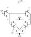
유기 발광 다이오드 디스플레이에서, 각 디스플레이 픽셀은 각각의 유기 발광 다이오드를 포함한다. 예시적인 유기 발광 다이오드 디스플레이 픽셀(22-1)의 개략도가 도 2에 도시된다. 도 2에 도시된 바와 같이, 디스플레이 픽셀(22-1)은 발광 다이오드(26)를 포함할 수 있다. 양의 전원 전압(ELVDD)은 양의 전원 단자(34)에 공급될 수 있고, 접지 전원 전압(ELVSS)은 접지 전원 단자(36)에 공급될 수 있다. 구동 트랜지스터(28)의 상태는 다이오드(26)를 통해 흐르는 전류의 양, 따라서 디스플레이 픽셀(22-1)로부터 방출된 광(40)의 양을 제어한다.In an organic light emitting diode display, each display pixel includes a respective organic light emitting diode. A schematic diagram of an exemplary organic light emitting diode display pixel 22-1 is shown in FIG. As shown in FIG. 2, the display pixel 22-1 may include a
트랜지스터(28)는 데이터의 연속적인 프레임들 사이에서 원하는 상태로 유지됨을 보장하기 위하여, 디스플레이 픽셀(22-1)은 저장 커패시터(Cst)와 같은 저장 커패시터를 포함할 수 있다. 저장 커패시터(Cst) 상의 전압은 노드(A)에서 트랜지스터(28)의 게이트에 인가되어 트랜지스터(28)를 제어한다. 데이터는 스위칭 트랜지스터(30)와 같은 하나 이상의 스위칭 트랜지스터를 사용하여 저장 커패시터(Cst)로 로딩될 수 있다. 스위칭 트랜지스터(30)가 오프일 때, 데이터 라인(D)은 저장 커패시터(Cst)로부터 절연되고, 단자(A) 상의 게이트 전압은 저장 커패시터(Cst)에 저장된 데이터 값과 동일하다(즉, 디스플레이(14) 상에 표시되고 있는 디스플레이 데이터의 이전 프레임으로부터의 데이터 값). 디스플레이 픽셀(22-1)에 연결된 행 내의 게이트 라인(G)(때때로 스캔 라인으로 지칭됨)이 어써트되는 경우, 스위칭 트랜지스터(30)는 턴온될 것이고 데이터 라인(D) 상의 새로운 데이터 신호는 저장 커패시터(Cst) 내에 로딩될 것이다. 커패시터(Cst) 상의 새로운 신호는 노드(A)에서 트랜지스터(28)의 게이트에 인가됨으로써, 트랜지스터(28)의 상태를 조정하고 발광 다이오드(26)에 의해 방출되는 광(40)의 대응하는 양을 조정한다.Display pixel 22-1 may include a storage capacitor, such as storage capacitor Cst, to ensure that
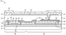
도 2의 픽셀(22-1)과 같은 유기 발광 다이오드 디스플레이 픽셀들은 도 3에 도시된 유형의 박막 트랜지스터 구조체들을 사용할 수 있다. 이러한 유형의 구조체에서, 2개의 상이한 유형들의 반도체가 사용된다. 도 3에 도시된 바와 같이, 회로(72)는 발광 다이오드 캐소드 단자(42) 및 발광 다이오드 애노드 단자(44)와 같은 디스플레이 픽셀 구조체들을 포함할 수 있다. 유기 발광 다이오드 방출 재료(47)는 캐소드(42)와 애노드(44) 사이에 개재될 수 있다. 유전체 층(46)은 디스플레이 픽셀의 레이아웃을 정의하는 기능을 할 수 있고 때때로 픽셀 정의 층으로 지칭될 수 있다. 편광 층(50)은 박막 트랜지스터 구조체들(52)의 상부 상에 형성될 수 있다. 박막 트랜지스터 구조체들(52)은 기판(24) 상의 버퍼 층(54) 상에 형성될 수 있다.Organic light emitting diode display pixels, such as pixel 22-1 of FIG. 2, may use thin film transistor structures of the type shown in FIG. In this type of structure, two different types of semiconductors are used. 3, the
박막 트랜지스터 구조체들(52)은 실리콘 트랜지스터(58)를 포함할 수 있다. 트랜지스터(58)는 "상부 게이트" 설계를 사용하여 형성되는 LTPS 트랜지스터일 수 있으며 유기 발광 다이오드 디스플레이 픽셀 내에서 스위칭 트랜지스터로서 기능할 수 있다(예컨대, 도 2의 픽셀(22-1) 내의 트랜지스터(30)를 참조). 트랜지스터(58)는 게이트 절연체 층(64)(예컨대, 실리콘 산화물 층)에 의해 덮인 폴리실리콘 채널(62)을 가질 수 있다. 게이트(66)는 패터닝된 금속(예컨대, 예로서 몰리브덴)으로 형성될 수 있다. 게이트(66)는 층간 유전체 층(예컨대, 실리콘 질화물 층(68) 및 실리콘 산화물 층(70))에 의해 덮일 수 있다. 소스-드레인 콘택들(74, 76)은 폴리실리콘 층(62)의 대향 측들을 접촉하여 실리콘 박막 트랜지스터(58)를 형성할 수 있다.The thin
박막 트랜지스터 구조체들(52)은 또한 박막 트랜지스터 및 커패시터 구조체들(60)을 포함할 수 있다. 구조체들(60)은 저장 커패시터(즉, 도 2의 저장 커패시터(Cst)) 및 산화물 박막 트랜지스터 구조체를 포함할 수 있다. 저장 커패시터는 폴리실리콘 층(62')(층(62)과 동일한 층의 일부로서 패터닝됨)으로 형성된 제1 단자(때로는 플레이트, 전극 또는 전극 층으로 지칭됨)를 가질 수 있다. 게이트 절연체 층(64)의 연장된 일부일 수 있는 게이트 절연체 층(64')은 단자(62')를 덮을 수 있다. 커패시터는 금속 층(66')으로 형성된 제2 단자를 가질 수 있다. 금속 층(66')은 트랜지스터(58)의 게이트(66)의 형성 시에 사용된 동일한 금속 층으로 패터닝될 수 있다. 유전체 층들(68, 70)은 금속 층(66')을 덮을 수 있다. 구조체들(60) 내의 박막 트랜지스터는 "하부 게이트" 산화물 트랜지스터일 수 있다. 커패시터(Cst)의 제2 단자(즉, 도 2의 노드(A))로서 기능하는 층(66')은 또한 산화물 트랜지스터의 게이트로서 기능할 수 있다. 산화물 트랜지스터는 도 2의 구동 트랜지스터(28)로서 기능할 수 있다. 산화물 트랜지스터의 "게이트 절연체"는 층간 유전체 층(즉, 층들(68, 70)으로 형성될 수 있다. 산화물 트랜지스터의 채널 반도체는 산화물 층(80)(예컨대, IGZO)으로 형성될 수 있다. 산화물 층(80)은 폴리실리콘 커패시터 전극 층(62')과 중첩함으로써(즉, 산화물 트랜지스터가 커패시터와 중첩함으로써), 공간을 절약할 수 있다. 소스-드레인 단자들(82, 84)은 반도체성 산화물 층(80)의 대향 단부들을 접촉하는 금속으로 형성될 수 있다.The thin
LTPS 트랜지스터 및 산화물 트랜지스터와 같은 트랜지스터들이 상이한 레이아웃으로 형성될 수 있다. 예를 들면, LTPS 트랜지스터는 높은 캐리어 이동도를 갖는 경향이 있다. 그 결과, LTPS 트랜지스터는 이러한 트랜지스터들의 상대적으로 높은 이동도를 보상하기 위해 낮은 비의 W/L을 적절하게 보장하도록 상대적으로 긴 게이트 길이(L) 및 상대적으로 짧은 게이트 폭을 가질 수 있다. 이는 LTPS 트랜지스터들로 하여금 픽셀 레이아웃에 대해 상대적으로 불충분하게 되게 할 수 있다. 산화물 트랜지스터들은 더 작은 종횡비를 갖는 W/L 비로 구성될 수 있다(예컨대, LTPS에 대해 3/30와 비교하여 산화물에 대해 4/4). 이러한 레이아웃 효율성 고려사항들에 기인하여, 디스플레이 픽셀들(22-1)에서 구동 트랜지스터들로서 산화물 트랜지스터들을 사용하는 것이 바람직할 수 있다. LTPS 트랜지스터에 의해 제공된 상대적으로 신속한 스위칭 속도는 도 2의 트랜지스터(30)와 같은 스위칭 트랜지스터에 LTPS 트랜지스터를 사용하는 것이 바람직하게 만들 수 있다.Transistors such as LTPS transistors and oxide transistors can be formed in different layouts. For example, LTPS transistors tend to have high carrier mobility. As a result, the LTPS transistor can have a relatively long gate length (L) and a relatively short gate width to adequately ensure a low ratio of W / L to compensate for the relatively high mobility of these transistors. This may cause the LTPS transistors to be relatively insufficient for the pixel layout. The oxide transistors can be configured with a W / L ratio with a smaller aspect ratio (e.g., 4/4 for oxide compared to 3/30 for LTPS). Due to these layout efficiency considerations, it may be desirable to use oxide transistors as the driving transistors in the display pixels 22-1. The relatively fast switching speed provided by the LTPS transistor may make it desirable to use an LTPS transistor in a switching transistor such as
더 많은 트랜지스터(예컨대, 3개 이상, 4개 이상, 5개 이상, 6개 이상, 7개 이상, 또는 8개 이상)를 갖는 디스플레이 픽셀들에서, 트랜지스터가 LTPS 기술을 사용하여 구현되고 트랜지스터가 산화물 기술을 사용하여 구현되는 선택은 2개의 유형의 트랜지스터들 사이에서 트랜지스터 성능 고려사항들을 균형잡히게 하도록 이루어질 수 있다.In display pixels having more transistors (e.g., three or more, four or more, five or more, six or more, seven or more, or eight or more), transistors are implemented using LTPS technology, ≪ / RTI > techniques can be made to balance transistor performance considerations between the two types of transistors.
구동 트랜지스터를 구현하는 경우, LTPS 트랜지스터는 산화물 트랜지스터보다 큰 크기(더 긴 채널 길이)를 보여주는 경향이 있고, 산화물 트랜지스터보다 더 큰 암전류를 보여주는 경향이 있으며, 산화물 트랜지스터보다 열악한 균일성을 보일 수 있다. LTPS 구동 트랜지스터는 또한 산화물 구동 트랜지스터보다 더 많은 히스테리시스를 보일 수 있다. 이러한 요인들의 결과로, 산화물 트랜지스터로부터 유기 발광 다이오드 디스플레이 픽셀 내에 구동 트랜지스터를 형성하는 데 종종 이점이 될 수 있다. 산화물 구동 트랜지스터는 낮은 누설 전류 및 최소 히스테리시스를 보일 수 있다.When implementing a driving transistor, the LTPS transistor tends to show a larger size (longer channel length) than the oxide transistor, tends to exhibit a larger dark current than the oxide transistor, and may exhibit poorer uniformity than the oxide transistor. The LTPS driving transistor may also exhibit more hysteresis than the oxide driving transistor. As a result of these factors, it can often be advantageous to form a drive transistor within the organic light emitting diode display pixel from the oxide transistor. The oxide drive transistor may exhibit low leakage current and minimal hysteresis.
스위칭 트랜지스터를 구현하는 경우, LTPS 트랜지스터는 산화물 트랜지스터보다 더 작을 수 있고, 산화물 트랜지스터보다 더 적은 양의 기생 커패시턴스를 보일 수 있으며, 산화물 트랜지스터보다 더 낮은 전력 소비를 보일 수 있다. 이들과 같은 요인들의 결과로, LTPS 트랜지스터로부터 유기 발광 다이오드 디스플레이 픽셀 내에 스위칭 트랜지스터를 형성하는 데 종종 이점이 될 수 있다. LTPS 스위칭 트랜지스터는 높은 스위칭 속도 및 낮은 기생 커패시턴스를 보일 수 있다.When implementing a switching transistor, the LTPS transistor may be smaller than the oxide transistor, may exhibit a smaller amount of parasitic capacitance than the oxide transistor, and may exhibit lower power consumption than the oxide transistor. As a result of these factors, it can often be advantageous to form a switching transistor within an OLED pixel from an LTPS transistor. LTPS switching transistors can exhibit high switching speeds and low parasitic capacitance.
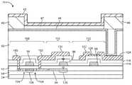
단일의 유기 발광 다이오드 디스플레이 픽셀 내의 LTPS 및 산화물 트랜지스터 둘 다를 구현하는 데 사용될 수 있는(예컨대, 도 2의 디스플레이 픽셀 회로(22-1)와 같은 회로를 구현하기 위해) 예시적인 하이브리드 박막 트랜지스터 구조체가 도 4에 도시된다. 도 4의 하이브리드 박막 트랜지스터 구조체들(114)은 실리콘 박막 트랜지스터(108), 커패시터(Cst, 110) 및 산화물 트랜지스터(112)를 포함한다. 실리콘 트랜지스터(108)는 폴리실리콘 층(90)으로 형성된다. 게이트 절연체 층(92)은 폴리실리콘 층(90)을 덮는다. 게이트 금속 층은 게이트 절연체 층(92)의 상부에 패터닝되어, 게이트(94), 커패시터 전극(96) 및 게이트 전극(98)을 형성한다. 실리콘 질화물 층(116) 및 실리콘 산화물 층(118)과 같은 층간 유전체 재료의 층은 패터닝된 게이트 금속 구조체들을 덮을 수 있다. 실리콘 트랜지스터(108)를 위한 소스-드레인 콘택들(100, 94)은 채널 영역(106)의 부근에서 폴리실리콘 층(90)을 접촉할 수 있다(즉, 단락될 수 있다). 트랜지스터(108)의 게이트(94)는 저밀도 드레인 주입들로 하여금 트랜지스터(108)의 폴리실리콘 채널 영역(106)에 인접한 영역들(104)에서 폴리실리콘 층(90) 내에 형성되게 하는 주입 마스크로서 기능할 수 있다.An exemplary hybrid thin film transistor structure (e.g., to implement a circuit such as display pixel circuit 22-1 of FIG. 2) that can be used to implement both LTPS and oxide transistors in a single organic light emitting diode display pixel 4. The hybrid thin
실리콘 트랜지스터(108)의 소스-드레인들(100, 102), 커패시터 전극(120), 및 산화물 트랜지스터(112)의 소스-드레인들(122, 124)은 층간 유전체(116, 118) 상에 공통 금속 층의 패터닝된 부분들로 형성될 수 있다.The source-
커패시터(110)는 금속 전극(120)으로 그리고 폴리실리콘 층(90)의 부분(126)으로 형성된 제1 단자를 가질 수 있다. 커패시터(110)는 금속 전극(96)으로 형성된 제2 단자를 가질 수 있다.
산화물 트랜지스터(112)는 IGZO 층(128)과 같은 반도체 산화물 층, 소스-드레인 콘택들(122, 124), 및 게이트(98)를 가질 수 있다. 게이트(98)는 트랜지스터(112)를 위한 채널 영역으로서 기능하는 반도체 산화물(128)로부터 유전체(116, 118)에 의해 분리된다. 따라서, 유전체(116, 118)는 산화물 트랜지스터(112)를 위한 게이트 절연체로서 기능한다.The
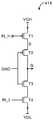
도 5는 디스플레이(14)에 사용될 수 있는 다른 예시적인 유기 발광 다이오드 픽셀 회로의 회로도이다. 픽셀(22-2)은 발광 다이오드(26)에 전류를 공급하기 위한 구동 트랜지스터(28)를 포함한다. 저장 커패시터(Cst)는 프레임들 사이의 트랜지스터(28)의 게이트 상에 신호들을 저장하는 데 사용된다. 감지 라인(감지)은 트랜지스터 성능에서 픽셀간 변동을 조정하기 위하여 보상 스킴을 구현하는 데 사용된다. 게이트 라인(스캔 및 스캔2)은 스위칭 트랜지스터들(30-1, 30-2)에 제어 신호들을 인가하는 데 사용된다.5 is a circuit diagram of another exemplary organic light emitting diode pixel circuit that may be used in the
디스플레이 픽셀(22-2)에서 성능을 최적화하기 위하여, 도 3 및 도 4에 도시된 유형의 하이브리드 구조체들 또는 실리콘 및/또는 산화물 박막 트랜지스터들 및 커패시터들을 형성하기 위한 다른 구성들을 사용하는 것이 바람직할 수 있다. 예를 들면, 산화물 트랜지스터(예컨대, NMOS 산화물 트랜지스터)로 구동 트랜지스터(28)를 형성하면서, 실리콘 트랜지스터들로 또는 실리콘 (NMOS 및/또는 PMOS)과 산화물(NMOS) 트랜지스터들의 혼합으로 트랜지스터들(30-1, 30-2)과 같은 스위칭 트랜지스터들을 형성하는 것이 바람직할 수 있다.To optimize performance at display pixel 22-2, it is desirable to use hybrid structures of the type shown in Figures 3 and 4 or other configurations for forming silicon and / or oxide thin film transistors and capacitors . For example, transistors 30-n may be formed with silicon transistors or with a mixture of silicon (NMOS and / or PMOS) and oxide (NMOS) transistors, while driving
제1 예시적인 구성에 따르면, 트랜지스터(30-1)는 산화물 트랜지스터이고, 트랜지스터(30-2)는 산화물 트랜지스터이며, 트랜지스터(28)는 산화물 트랜지스터이다. 제2 예시적인 구성에 따르면, 트랜지스터(30-1)는 실리콘 트랜지스터이고, 트랜지스터(30-2)는 실리콘 트랜지스터이며, 트랜지스터(28)는 산화물 트랜지스터이다. 도 3의 구조체 또는 도 4의 구조체와 같은 하이브리드 트랜지스터 구조체는 (예컨대, 트랜지스터(30-1, 28) 및 커패시터(Cst)를 구현하기 위한) 이러한 시나리오에 사용될 수 있다. 예시적인 제3 구성에 따르면, 트랜지스터(30-1)는 실리콘 트랜지스터이고, 트랜지스터(30-2)는 산화물 트랜지스터이며, 트랜지스터(28)는 산화물 트랜지스터이다. 제2 예시적인 구성과 마찬가지로, 도 3의 구조체 또는 도 4의 구조체와 같은 하이브리드 트랜지스터 구조체는 트랜지스터(30-1, 28) 및 커패시터(Cst)를 구현하는 데 사용될 수 있다.According to a first exemplary configuration, the transistor 30-1 is an oxide transistor, the transistor 30-2 is an oxide transistor, and the
원하는 경우, 디스플레이(14)는 액정 디스플레이일 수 있다. 이러한 유형의 시나리오에서, 디스플레이(14)의 각 픽셀은 디스플레이 내의 액정 층의 연결 부분에 전계를 인가하기 위한 전극 구조체, 이미지 데이터의 프레임들 사이에 전극 상에 전하를 저장하기 위한 커패시터, 및 전극들로의 전계의 인가를 제어하기 위한 박막 트랜지스터를 포함할 수 있다. 하나의 적절한 배열에 따르면, 액정 디스플레이 내의 게이트 구동 회로(18) 및 디멀티플렉서 회로(20)(도 1)는 실리콘 트랜지스터들로 형성될 수 있고, 디스플레이 픽셀들(22) 내의 박막 트랜지스터들은 산화물 트랜지스터들로 형성될 수 있다. 실리콘 트랜지스터들은 높은 이동 채널 영역들을 가지며, 저전압 및 저전력에서 동작하는 동안 신속한 스위칭 속도 및 높은 구동 전류에 아주 적합하다. 디스플레이 픽셀들(22) 내의 산화물 박막 트랜지스터들은 낮은 누설 전류를 보인다.If desired, the
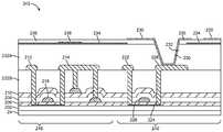
실리콘 및 산화물 트랜지스터들 둘 다를 갖는 액정 디스플레이를 형성하는 데 사용될 수 있는 유형의 박막 트랜지스터 구조체들은 도 6에 도시된다. 도 6에 도시된 바와 같이, 박막 트랜지스터 구조체들(242)은 실리콘 박막 트랜지스터 구조체들(216)(예컨대, 디스플레이 구동 회로(18) 및 디멀티플렉서 회로(20)와 같은 주변 회로들의 일부를 형성하기 위하여) 및 산화물 박막 트랜지스터 구조체들(240)(예컨대, 도 1의 디스플레이(14)에 의해 도시된 유형의 레이아웃을 갖는 액정 디스플레이 내에 디스플레이 픽셀들(22)을 형성하기 위하여)을 포함할 수 있다.A thin film transistor structure of the type that can be used to form a liquid crystal display having both silicon and oxide transistors is shown in FIG. 6, thin
구조체들(216, 240)은 기판(24) 상의 버퍼 층(202) 상에 형성될 수 있다. 폴리실리콘 층(204)은 버퍼(202) 상에 퇴적될 수 있다. 게이트 절연체 층(206)은 폴리실리콘 층(204) 상에 형성될 수 있다. 공통 금속 층은 패터닝되어 금속 구조체들(218, 220, 228)을 형성할 수 있다. 구조체(218)는 폴리실리콘(204)으로 형성된 채널 및 소스-드레인 콘택들(212, 214)을 포함하는 실리콘 트랜지스터를 위한 게이트로서 기능할 수 있다. 금속 구조체(228)는 반도체성 산화물 층(224)(예컨대, IGZO) 및 소스-드레인 단자들(222, 226)로 형성된 산화물 트랜지스터를 위한 게이트로서 기능할 수 있다. 금속 구조체(228)는 또한 디스플레이(14) 내의 백라이트가 산화물 층(224)에 도달하는 것을 방지하는 것을 돕는 광 차폐체로서 기능할 수 있고, 따라서 별도의 광 차폐 구조체들이 구조체들(240)에 통합될 필요가 없다. 실리콘 질화물 층(208, 210)과 같은 층간 유전체는 구조체(216) 내의 게이트(218)를 덮을 수 있고, 구조체들(240)의 산화물 트랜지스터 내의 게이트(228)를 위한 게이트 절연체로서 기능할 수 있다.
금속(230)은 산화물 층(224)으로 형성된 디스플레이 픽셀 박막 산화물 트랜지스터의 소스-드레인(226)을 접촉한다. 금속(230)은 유기 층(232)에 의해 지지될 수 있다. 유기 층(232)의 표면 상에, 금속(230)은 다수의 핑거들을 갖는 전극을 형성할 수 있다. 유전체 층(236)은 공통 전극(Vcom)(234)으로부터 전극(230)을 분리할 수 있다. 동작 동안, 전계는 전극(230)과 전극(234) 사이에 생성된다. 이러한 전계는 디스플레이 내의 액정 재료를 통과한다. 원하는 경우, 디스플레이(14)는 Vcom 전극(234)의 부분들로 형성된 용량성 터치 센서들을 통합할 수 있다. 이러한 유형의 구성에서, 라인(238)과 같은 옵션의 금속 라인들은 전극(234)의 형성 시에 사용된 재료(예를 들면, 인듐 주석 산화물과 같은 다소 저항성의 전도성 재료일 수 있음)의 저항을 줄이는 것을 돕기 위해 사용될 수 있다.The
층들(208, 210)의 두께는 약 6000 옹스트롬일 수 있다. 이러한 상대적으로 큰 두께는 게이트(218)와 소스-드레인(214)과 같은 근처의 금속 구조체들 사이의 커패시턴스를 최소화하는 것을 도울 수 있지만, 산화물 트랜지스터에서 스위칭 속도를 제한할 수 있다. 이러한 우려를 해결하기 위하여, 도 7의 구조체들(242')에 의해 사용된 유형의 설계가 사용될 수 있다. 도 7 배열에 따르면, 추가의 반도체 제조 마스크는 게이트(218)의 형성 시에 사용된 금속 층과 별개의 금속 층으로 형성된 산화물 트랜지스터를 위한 게이트를 생성하는 데 사용될 수 있다. 이러한 접근에 따르면, (예를 들면, 실리콘 질화물 및 실리콘 산화물의 서브 층들로 형성된) 단일의 3000 옹스트롬 유전체 층(210')만이 산화물 층(224)으로부터 산화물 트랜지스터 게이트(228')를 분리하는 데 사용되고, 따라서 산화물 트랜지스터 스위칭 속도는 향상될 수 있다. 도 7의 구조체들(242')의 배열은 게이트(218) 및 게이트(228')로 하여금 상이한 금속들로 형성되게 한다. 예를 들면, 게이트(218)는 실리콘 트랜지스터를 활성화시키는 것과 연결된 상승된 온도를 수용하도록 Mo와 같은 내화 금속으로 형성될 수 있는 반면, 게이트(228')는 구리와 같은 더 낮은 저항성 금속으로 형성될 수 있다.The thickness of the
일부 응용들에서, 높은 구동 전압(게이트-대-소스 및 드레인)을 처리하는 것이 고려될 필요가 있을 수 있다. 도 8의 트랜지스터 구조체들(242'')은 실리콘 트랜지스터 게이트 상에서 상대적으로 더 큰(예컨대, 20 볼트) 스윙을 처리하는 것이 바람직한 시나리오들에 사용될 수 있다. 이러한 상황에서, 게이트 절연체 층(206)은 20 볼트 신호로부터의 손상을 견디기에는 불충분하게 얇을 수 있다. 예를 들면, 게이트 절연체(206)는 20 볼트 구동 전압을 확실하게 처리하기 위해 충분히 두껍지 않을 수 있는 약 800 옹스트롬 두께일 수 있다. 게이트 절연체 층(206)이 과도하게 응력을 받지 않는 것을 보장하기 위하여, 게이트 구조체(218)는 플로팅(전기적으로 절연된) 금속 구조체로 전환될 수 있고, 추가의 금속 층(즉, 패터닝되어 산화물 트랜지스터(240)의 게이트(228')를 형성하는 동일한 금속 층의 일부)은 실리콘 트랜지스터 게이트(218')의 형성 시에 사용될 수 있다. 플로팅 게이트(218)가 실리콘 트랜지스터(216)의 동작 동안 제어 신호들에 의해 구동되지 않더라도, 플로팅 게이트(218)는 폴리실리콘 층(204)의 소스 및 드레인 콘택 부분들로 이루어진 저밀도 드레인(LDD) 주입을 위한 마스크로서 기능하도록 유지될 수 있다.In some applications, it may be necessary to consider processing high driving voltages (gate-to-source and drain). The
하이브리드 실리콘/산화물 액정 디스플레이에서, 실리콘 트랜지스터들로부터 게이트 구동 회로(18) 및 디멀티플렉서 회로(20)와 같은 디스플레이 구동 회로를 형성할 필요가 없다. 원하는 경우, 이러한 디스플레이 구동 회로의 일부는 산화물 트랜지스터들로 형성될 수 있다. 예를 들면, 도 9의 예시적인 CMOS 인버터(300)와 같은 디스플레이(14)의 주변 회로에서 낮은 구동 전류 CMOS형 회로는 산화물 트랜지스터들을 포함할 수 있다. PMOS 산화물 트랜지스터들을 형성하는 것은 도전과제일 수 있고, 따라서 원하는 경우, 인버터(300)와 같은 회로들은 NMOS 산화물 트랜지스터 및 PMOS 실리콘 트랜지스터(예로서)를 사용하여 형성될 수 있다.In the hybrid silicon / oxide liquid crystal display, it is not necessary to form a display drive circuit such as the
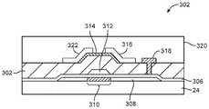
도 10의 예시적인 박막 트랜지스터 구조체들(302)과 같은 하이브리드 산화물-실리콘 박막 트랜지스터 구조체들은 게이트 구동 회로(18) 및 디멀티플렉서 회로(20)와 같은 디스플레이 구동 회로 내에 CMOS형 회로를 형성하는 데 사용될 수 있다. 도 10에 도시된 바와 같이, 구조체들(302)은 기판(24) 상에 형성된 폴리실리콘 층(308)을 가질 수 있다. P 채널 활성 영역(310)은 게이트(312) 아래에 형성될 수 있다. 게이트 절연체 층(306)(예컨대, 실리콘 산화물)은 실리콘 층(308)에서 실리콘 채널 영역(310)으로부터 게이트(312)를 분리할 수 있다. 유전체 층(302)(예컨대, 실리콘 산화물 및 실리콘 질화물의 서브층들)은 게이트(312)를 덮을 수 있다. 유전체 층(306)은 산화물 층(312)과 중첩하는 것으로부터 게이트(312)를 분리할 수 있다. 산화물 층(312)은 IGZO 재료와 같은 반도체성 산화물일 수 있다. 게이트(312)는 제1 패터닝된 금속 층으로 형성될 수 있다. 제2 패터닝된 금속 층은 출력 단자(322), 소스 단자(316), 및 드레인 단자(318)를 형성하는 데 사용될 수 있다. 패시베이션 층(320)은 단자들(316, 312)을 덮을 수 있다. 게이트(312)는 몰리브덴, 몰리브덴 텅스텐, 텅스텐, 또는 다른 금속들과 같은 재료로 형성될 수 있다. 금속 구조체들(322, 316, 318)과 같은 구조체들을 형성하기 위한 금속은 알루미늄, 몰리브덴 등과 같은 금속으로 형성될 수 있다.Hybrid oxide-silicon thin film transistor structures, such as the exemplary thin
도 10의 배열에 따르면, 게이트(314)는 2개의 트랜지스터를 위한 공통(공유) 게이트로서 기능한다. 특히, 게이트(314)(예컨대, 도 9의 단자(Vin) 참조)는 실리콘 층(308)으로 형성된 PMOS 실리콘 트랜지스터(도 9의 트랜지스터(TP))를 위한 게이트, 및 산화물 층(312)으로 형성된 NMOS 산화물 트랜지스터(도 9의 트랜지스터(TN))를 위한 게이트 둘 다로서 기능한다. 산화물 층(312)은 게이트(314) 위에 위치되고, 실리콘 층(310)은 게이트(314) 아래에 위치된다. 도 10의 공유 게이트 배열은 도 9에 도시된 유형의 CMOS 인버터로 하여금 콤팩트하게 구현되게 한다.According to the arrangement of Figure 10,
도 11은 액정 디스플레이 상에서 사용될 수 있는 예시적인 게이트 구동 회로(18)를 도시한다. 회로(18)는 게이트 신호들에 의해 구동되고 있는 디스플레이 픽셀들(22) 내의 산화물 박막 트랜지스터들의 만족스러운 동작을 보장하기 위하여 더 큰 전압 스윙(예컨대, 20 볼트 스윙 이상)에 의해 게이트 신호들(G)을 생성하면서, 실리콘 트랜지스터들에 대한 상대적으로 작은 전압 스윙(예컨대, 15 볼트 또는 16 볼트 스윙)을 갖는 신호들을 사용할 수 있다.Figure 11 shows an exemplary
도 11에 도시된 바와 같이, 회로(18)는 일련의 연결된 SR 래치들(400) 또는 다른 레지스터 회로들로 형성된 시프트 레지스터를 가질 수 있다. 도 11에서 회로의 각 행은 액정 디스플레이의 디스플레이 픽셀들(22)의 별도의 행과 연결되고, 디스플레이 픽셀들의 그 행에 대한 각각의 게이트 신호(G)를 제공한다. 동작 동안, 트리거 신호(트리거)는, 클록 신호(로드 클록)가 시프트 레지스터에 인가되고 있는 동안, 회로(18) 내의 시프트 레지스터의 제1 행 내의 래치에 인가될 수 있다. 트리거 신호는 캐스캐이딩 신호(cascading signal)로 하여금 시프트 레지스터를 통해 리플 다운(ripple down)하게 한다. 이에 응답하여, 각 래치(400)는 순차적으로 자신의 출력(OUT)을 어써트한다. 게이트 구동 회로(18)의 각 행은 출력 신호(OUT)를 수신하는 각각의 레벨 시프터(404) 및 버퍼(404)를 갖는다.As shown in FIG. 11,
출력 신호(OUT)는 15V(또는 다른 적합한 전압)의 높은 전압 내지 0 볼트(또는 다른 적합한 전압)의 범위 내에 있다. 이러한 유형의 구성과 연관된 15 볼트 스윙은 래치들(400)에 실리콘 박막 트랜지스터에 의해 용인될 수 있는 반면, 20 볼트 스윙과 같은 더 큰 전압 스윙이 실리콘 박막 트랜지스터에 과도하게 응력을 가할 수 있다. 레벨 시프터(402)는 래치(400)로부터 15 볼트 내지 0 볼트 신호(OUT)를 시프트하여, 레벨 시프터(402)로부터 경로(406) 상의 출력은 5 볼트 내지 -11 볼트의 범위 내에 있게 된다(즉, 레벨 시프터(402)에서 실리콘 트랜지스터에 의해 용인될 수 있는 16 볼트의 스윙). 버퍼(404)는 래치(400)로부터 입력 신호(IN_H)로서 15 볼트 내지 0 볼트 신호(OUT)를 수신하고 입력 신호(IN_L)로서 5 볼트 내지 -11 볼트 신호를 수신한다. 버퍼(404)는 바람직하게 실리콘 박막 트랜지스터들을 포함한다. 버퍼(404)의 설계는 버퍼(404)로 하여금 액정 디스플레이 상에 디스플레이 픽셀들(22)의 어레이 내의 산화물 트랜지스터들을 제어하기에 적절한 유형의 큰 전압 스윙(예컨대, 15 볼트 내지 -11 볼트)을 갖는 출력 신호(게이트 라인 신호(G))를 생성하게 한다.The output signal OUT is in the range of high voltage to 0 volts (or other suitable voltage) of 15 volts (or other suitable voltage). A 15 volt swing associated with this type of configuration can be tolerated by silicon thin film transistors in the
도 12는 레벨 시프터(402)를 구현하는 데 사용될 수 있는 유형의 예시적인 회로의 회로도이다. 래치(400)의 출력(OUT)으로부터의 신호들은 레벨 시프터(402)의 입력(410)에서 수신될 수 있고, 버퍼(404)에 대한 대응하는 레벨-시프트된 출력 신호들(신호들(IN_L))은 레벨 시프터(402)의 출력(412)에서 제공될 수 있다. 원하는 경우 다른 레벨 시프터 설계들이 레벨 시프터(402)에 사용될 수 있다. 도 12의 구성은 단지 예시적인 것이다. 실리콘 박막 트랜지스터들은 레벨 시프터(402)를 형성하는 데 사용될 수 있다.12 is a circuit diagram of an exemplary circuit of the type that may be used to implement
도 13의 회로(404)는 도 11의 버퍼(404)를 구현하는 데 사용될 수 있는 설계의 예이다. 이러한 설계에 따라, 신호들(IN_H, IN_L)은 상이한 각각의 전압 스윙들을 갖는 동일한 구형파 펄스들이다. 신호(IN_H)는 15 내지 0 볼트의 범위 내에 있다. 신호(IN_L)는 5 내지 -11 볼트의 범위 내에 있다. 이러한 예에서 대응하는 출력 신호(게이트 라인 신호)(G)는 15볼트 내지 -11볼트의 범위 내에 있는 구형파 펄스이므로, 20 볼트 초과의 스윙을 갖는다.The
접지 전압(GND)은 트랜지스터들(T2, T3)의 게이트들에 인가된다. 이는 회로(414)의 출력 스윙이 20 볼트를 초과하더라도, 약 16 볼트 미만으로 회로(414)의 트랜지스터들이 겪는 그 최대 전압을 제한한다. 트랜지스터들(T2, T3)의 게이트들 상의 접지 전압(GND)은 이러한 트랜지스터들로 하여금 과도한 소스 단자 전압 스윙이 검출되는 경우에는 언제든지 트랜지스터들(T1, T4)을 보호하도록 턴오프하게 한다. 예로서, 트랜지스터들(T1, T2)을 고려해 보자. 트랜지스터(T2)는 문턱 전압(Vth)에 의해 특정지어질 수 있다. 트랜지스터(T1)의 소스(S)가 전압(GND) 아래(― Vth)로 떨어지기 시작하는 경우, 트랜지스터(T2)는 트랜지스터(T1)를 턴오프하고 절연할 것이다. 트랜지스터들(T3, T4)은 동일한 방식으로 동작한다. 이러한 배열을 사용하여, 버퍼(414) 내의 트랜지스터들 중 어느 것도 과도한 전압 스윙에 노출되지 않고, 이는 트랜지스터들(T1, T2, T3, T4)인 실리콘 박막 트랜지스터들로 형성되게 한다.The ground voltage GND is applied to the gates of the transistors T2 and T3. This limits its maximum voltage experienced by the transistors of
원하는 경우, 다른 회로 구성들은 게이트 구동 회로(18)로 하여금 게이트 라인 신호(G)가 디스플레이 픽셀들(22) 내의 산화물 트랜지스터들을 수용하도록 큰 전압 스윙을 갖는 환경에서 동작하게 하는 데 사용될 수 있다. 예로서, 레벨 시프터 트랜지스터들의 서브세트 및 출력 버퍼 트랜지스터들의 서브세트는 실리콘 박막 트랜지스터 구조체들을 사용하는 것에 부가하여 산화물 박막 트랜지스터 구조체들을 사용하여 구현될 수 있다.Other circuit configurations, if desired, may be used to cause the
도 14는 액정 디스플레이에 사용될 수 있는 유형의 추가의 박막 트랜지스터 회로의 측단면도이다. 도 14에 도시된 바와 같이, 박막 트랜지스터 구조체들(242)은 실리콘 박막 트랜지스터 구조체들(216)(예컨대, 디스플레이 구동 회로(18) 및 디멀티플렉서 회로(20)와 같은 주변 회로들의 일부를 형성하기 위함) 및 산화물 박막 트랜지스터 구조체들(240)(예컨대, 도 1의 디스플레이(14)에 의해 도시된 유형의 레이아웃을 갖는 액정 디스플레이 내에 디스플레이 픽셀들(22)을 형성하기 위함)을 포함할 수 있다.14 is a side cross-sectional view of an additional thin film transistor circuit of a type that can be used in a liquid crystal display. 14, thin
구조체들(216, 240)은 기판(24) 상의 버퍼 층(202) 상에 형성될 수 있다. 폴리실리콘 층(204)은 버퍼(202) 상에 퇴적될 수 있다. 게이트 절연체 층(206)은 폴리실리콘 층(204) 상에 형성될 수 있다. 공통 금속 층은 패터닝되어 금속 구조체들(218, 220, 228)을 형성할 수 있다. 구조체(218)는 폴리실리콘(204)으로 형성된 채널 및 소스-드레인 콘택들(212, 214)을 포함하는 실리콘 트랜지스터를 위한 게이트로서 기능할 수 있다. 금속 구조체(228)는 반도체성 산화물 층(224)(예컨대, IGZO) 및 소스-드레인 단자들(222, 226)로 형성된 산화물 트랜지스터를 위한 게이트로서 기능할 수 있다. 금속 구조체(228)는 또한 디스플레이(14) 내의 백라이트가 산화물 층(224)에 도달하는 것을 방지하는 것을 돕는 광 차폐체로서 기능할 수 있고, 따라서 별도의 광 차폐 구조체들이 구조체들(240)에 통합될 필요가 없다. 실리콘 질화물 층(208, 210)과 같은 층간 유전체는 구조체(216) 내의 게이트(218)를 덮을 수 있고, 구조체들(240)의 산화물 트랜지스터 내의 게이트(228)를 위한 게이트 절연체로서 기능할 수 있다.
금속 구조체들(218, 220, 228) 및 상호접속 라인(502)과 같은 라우팅 라인들은 제1 금속 층(때때로 M1 층으로 지칭됨)으로 형성될 수 있다. 구조체들(240)의 산화물 트랜지스터를 위한 소스-드레인 콘택들을 형성하는 금속(222, 226) 및 상호접속 라인(500)과 같은 라우팅 라인들은 제2 금속 층(때때로 SD1 층으로 지칭됨)으로 형성될 수 있다. 금속 구조체들(212, 214) 및 상호접속 라인(506)과 같은 라우팅 라인들은 제3 금속 층(때때로 SD2 층으로 지칭됨)으로 형성될 수 있다. 유전체 층들(232B)은 제3 금속 층으로부터 제2 금속 층을 분리할 수 있다. 유전체 층(232A)은 금속 층(234)과 같은 금속 구조체들로부터 제3 금속 층을 분리할 수 있다.Routing lines such as
금속(230)은 금속 층(504)을 접촉함으로써, 산화물 층(224)으로 형성된 디스플레이 픽셀 박막 산화물 트랜지스터의 소스-드레인(226)에 결합된다. 금속(230)은 유기 층(232B)에 의해 지지될 수 있다. 유기 층(232B)의 표면 상에, 금속(230)은 다수의 핑거들을 갖는 전극을 형성할 수 있다. 유전체 층(236)은 공통 전극(Vcom)(234)으로부터 전극(230)을 분리할 수 있다. 동작 동안, 전계는 전극(230)과 전극(234) 사이에 생성된다. 이러한 전계는 디스플레이 내의 액정 재료를 통과한다. 원하는 경우, 디스플레이(14)는 Vcom 전극(234)의 부분들로 형성된 용량성 터치 센서들을 통합할 수 있다. 이러한 유형의 구성에서, 라인(238)과 같은 옵션의 금속 라인들은 전극(234)의 형성 시에 사용된 재료(예를 들면, 인듐 주석 산화물과 같은 다소 저항성의 전도성 재료일 수 있음)의 저항을 줄이는 것을 돕기 위해 사용될 수 있다.The
디스플레이(14) 내의 라우팅 라인들 사이의 용량성 결합은 스위칭 손실들을 초래할 수 있다. 예로서, 소스-드레인 구조체(222)는 디스플레이(14) 내의 데이터 라인에 결합될 수 있다. 이러한 라인 상의 전압은 Vcom(전극(234))에 관하여 스위칭되고, 전력 손실을 초래할 수 있다. 유전체 층들(232A, 232B)의 존재는 데이터 라인과 Vcom 전극 사이에 용량성 결합을 감소시키는 것을 도울 수 있으므로, 전력 손실을 줄일 수 있다. 이러한 유전체 층들의 존재는 또한 디스플레이(14) 내의 라우팅 라인들 사이에 용량성 결합(예컨대, 라우팅 라인들과 제1 및 제2 금속 층들, 제1 및 제3 금속 층들 등의 다른 구조체들 사이에 용량성 결합)을 감소시킬 수 있다. 층들(232A, 232B)은 저유전율 유기 유전체 또는 다른 유전체 재료로 형성될 수 있다. 예로서, 층들(232A, 232B)은 아크릴 폴리머, 다른 폴리머들, 때때로 스핀-온-글래스로 지칭되는 유형의 유전체들(예컨대, 슬릿 코팅 도구들을 통해 퇴적된 스핀-온-글래스 폴리머들 등), 실록산-기반 재료들 등일 수 있다.Capacitive coupling between the routing lines in the
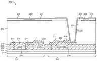
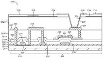
도 15는 상부 게이트 반도체성 산화물 트랜지스터를 포함하는 액정 디스플레이를 위한 예시적인 박막 트랜지스터 회로의 측단면도이다. 도 15에 도시된 바와 같이, 박막 트랜지스터 구조체들(242)은 실리콘 박막 트랜지스터 구조체들(216) 및 반도체성 산화물 박막 트랜지스터 구조체들(240)을 포함할 수 있다. 실리콘 박막 트랜지스터 구조체들(216)은 디스플레이 구동 회로(18) 및 디멀티플렉서 회로(20)와 같은 주변 회로들에 사용될 수 있고/있거나 액정 디스플레이의 디스플레이 픽셀들(22)을 위한 회로들을 형성하는 데 사용될 수 있다. 반도체성 산화물 박막 트랜지스터 구조체들(240)은 디스플레이 구동 회로(18) 및 디멀티플렉서 회로(20)와 같은 주변 회로들에 사용될 수 있고/있거나 액정 디스플레이의 디스플레이 픽셀들(22)을 위한 회로들을 형성하는 데 사용될 수 있다. 실리콘(폴리실리콘) 트랜지스터(216)와 같은 트랜지스터들은 n 채널 또는 p 채널 디바이스들일 수 있다. 반도체성 산화물 트랜지스터(240)와 같은 트랜지스터들은 n 채널 또는 p 채널 디바이스들일 수 있다.15 is a side cross-sectional view of an exemplary thin film transistor circuit for a liquid crystal display comprising a top gate semiconducting oxide transistor. As shown in FIG. 15, the thin
구조체들(216, 240)은 기판(24) 상의 버퍼 층(202) 상에 형성될 수 있다. 버퍼 층(202)은 무기 유전체와 같은 유전체로 형성될 수 있다. 버퍼 층(202)은 기판(24) 내의 이온들이 구조체들(216, 240) 내로 이동하는 것을 방지하는 것을 도울 수 있다.
폴리실리콘 층(204)은 버퍼(202) 상에 퇴적될 수 있다. 게이트 절연체 층(206)은 폴리실리콘 층(204) 상에 형성될 수 있다. 게이트 절연체 층(206)은 실리콘 산화물(예컨대, 100 nm 실리콘 산화물 층)과 같은 유전체로 형성될 수 있다. 공통 금속 층은 패터닝되어 금속 구조체들(218, 220, 228)을 형성할 수 있다. 구조체(218)는 폴리실리콘(204)으로 형성된 채널 및 소스-드레인 콘택들(212, 214)을 포함하는 실리콘 트랜지스터를 위한 게이트로서 기능할 수 있다. 금속 구조체(228)는 반도체성 산화물 층(224)(예컨대, IGZO)으로 형성된 상부 게이트 산화물 트랜지스터(즉, 반도체성 산화물 트랜지스터)를 위한 게이트 및 소스-드레인 단자들(222, 226)로서 기능할 수 있다. 층간 유전체(ILD)의 하나 이상의 층은 금속 구조체들(218, 220, 228)을 덮을 수 있다. 예를 들면, 층(208)과 같은 제1 유전체 층 및 층(210)과 같은 제2 유전체 층은 금속 구조체들(218, 220, 228)을 덮을 수 있다. 층(208)은 실리콘 질화물 층일 수 있고, 층(210)은 실리콘 산화물 층일 수 있다(예로서). 게이트(228)와 소스-드레인 전극들(222, 226) 사이에 어떠한 측면 중첩도 없기 때문에, 게이트(228)와 소스-드레인 구조체들(222, 226) 사이의 기생 커패시턴스는 최소화될 수 있다. 더욱이, 도 15의 산화물 트랜지스터의 층들(208, 210)은 도 14의 하부 게이트 산화물 트랜지스터 내의 층들(208, 210)보다 더 두꺼우므로, 기생 커패시턴스들을 추가로 감소시킬 수 있다.The
금속 구조체들(218, 220, 228)은 제1 금속 층(때때로 M1 층으로 지칭됨)으로 형성될 수 있다. 구조체들(240)의 산화물 트랜지스터를 위한 소스-드레인 콘택들을 형성하는 금속(222, 226), 및 구조체들(216)의 실리콘 트랜지스터를 위한 소스-드레인 콘택들을 형성하는 금속(212, 214)은 제2 금속 층(때때로 SD1 층 또는 M2 층으로 지칭됨)으로 형성될 수 있다. 금속 라인(238)과 같은 금속 구조체들은 제3 금속 층(때때로 M3 층으로 지칭됨)으로 형성될 수 있다. 유전체(232)(예컨대, 폴리머 층과 같은 유기 유전체 층)는 제3 금속 층으로부터 제2 금속 층을 분리할 수 있다.The
금속(230)은 산화물 층(224)으로 형성된 디스플레이 픽셀 박막 산화물 트랜지스터의 소스-드레인(226)을 접촉한다. 금속(230)은 유기 층(232)에 의해 지지될 수 있다. 유기 층(232)의 표면 상에, 금속(230)은 다수의 핑거들을 갖는 전극을 형성할 수 있다(예컨대, 디스플레이의 디스플레이 픽셀을 위한 픽셀 전극). 유전체 층(236)은 공통 전극(Vcom)(234)으로부터 전극(230)을 분리할 수 있다. 동작 동안, 전계는 전극(230)과 전극(234) 사이에 생성된다. 이러한 전계는 도 15의 구조체들의 상부 상에 형성된 디스플레이 내의 액정 재료를 통과한다. 원하는 경우, 디스플레이(14)는 Vcom 전극(234)의 부분들로 형성된 용량성 터치 센서들을 통합할 수 있다. 이러한 유형의 구성에서, 라인(238)과 같은 옵션의 금속 라인들은 전극(234)의 형성 시에 사용된 재료(예를 들면, 인듐 주석 산화물과 같은 다소 저항성의 전도성 재료일 수 있음)의 저항을 줄이는 것을 돕기 위해 사용될 수 있다.The
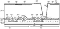
도 16에 도시된 바와 같이, 광 차폐체(520)와 같은 옵션의 광 차폐 구조체는 반도체성 산화물 트랜지스터(240)의 아래 또는 디스플레이 내의 어딘가에 형성될 수 있다. 광 차폐체(520)는 금속, 산화된 금속, 어두운 폴리머 또는 다른 광 차단 재료들과 같은 불투명 재료로 형성될 수 있다. 광 차폐체(520)의 존재는 미광(stray light)이 반도체성 산화물 트랜지스터 구조체들(240) 또는 다른 중첩하는 구조체들의 동작을 방해하는 것을 방지하는 것을 도울 수 있다.As shown in FIG. 16, an optional light shield structure, such as
도 17의 예에서, 도 15의 유전체 층(232)은 2개의 유전체 층들(232A, 232B)로 분할되었다. 층(232A)은 트랜지스터들(216, 240)의 소스-드레인 전극들과 중첩할 수 있다. 층(232B)은 소스-드레인 전극들과 소스-드레인 금속 층 및 층들(208, 210)로 형성된 다른 금속 구조체들 사이에 개재될 수 있다. 도 14와 관련하여 설명한 바와 같이, 이러한 유형의 2-층 접근은 디바이스들(216, 240)의 금속 구조체들 사이에 용량성 결합을 감소시킬 수 있다. 유기 발광 다이오드 디스플레이 내의 상부 게이트 반도체성 산화물 트랜지스터를 포함하는 예시적인 박막 트랜지스터 회로의 측단면도가 도 18에 도시된다. 도 18에 도시된 바와 같이, 회로(72)는 발광 다이오드 캐소드 단자(42) 및 발광 다이오드 애노드 단자(44)와 같은 디스플레이 픽셀 구조체들을 포함할 수 있다. 유기 발광 다이오드 방출 재료(47)는 캐소드(42)와 애노드(44) 사이에 개재될 수 있다. 픽셀 정의 층(46)은 디스플레이 픽셀의 레이아웃을 정의하도록 기능하는 유전체 층(46)일 수 있다. 층(46)은 미광을 차단하는 것을 돕기 위한 흑색 폴리머와 같은 폴리머로 형성될 수 있다.In the example of FIG. 17, the
편광 층(50)은 박막 트랜지스터 구조체들(52)의 상부 상에 형성될 수 있다. 박막 트랜지스터 구조체들(52)은 기판(24) 상의 버퍼 층(54) 상에 형성될 수 있다. 기판(24)은 금속, 유리, 폴리머, 다른 재료, 또는 이들 재료의 조합으로부터 형성될 수 있다. 버퍼 층(54)은 기판(24) 내의 이온들이 구조체들(52)의 동작을 방해하는 것을 방지하는 것을 돕는 무기 유전체 층으로 형성될 수 있다. 옵션의 기능성 층(522)은 버퍼 층(54)과 기판(24) 사이에 개재될 수 있다. 기능성 층(522)은 응력 완화 층, 광 차단 층, 커패시터와 같은 컴포넌트들의 형성 시에 사용된 층(예컨대, 픽셀 회로 및/또는 주변 회로를 위한 커패시터 전극들) 등일 수 있다.The
박막 트랜지스터 구조체들(52)은 실리콘 트랜지스터(58)를 포함할 수 있다. 트랜지스터(58)는 상부 게이트 설계를 사용하여 형성되는 LTPS 트랜지스터일 수 있으며 유기 발광 다이오드 디스플레이 픽셀 내에서 스위칭 트랜지스터로서 기능할 수 있다(예컨대, 도 2의 픽셀(22-1) 내의 트랜지스터(30)를 참조). 트랜지스터(58)는 또한 주변 회로들(예컨대, 구동 회로(18) 및 디멀티플렉서 회로(20))에 사용될 수 있다.The thin
트랜지스터(58)는 게이트 절연체 층(64)(예컨대, 100 nm 두께 또는 다른 적합한 두께를 갖는 실리콘 산화물 층)에 의해 덮인 폴리실리콘 채널(62)을 가질 수 있다. 게이트(66)는 패터닝된 금속(예컨대, 예로서 몰리브덴)으로 형성될 수 있다. 게이트(66)는 층간 유전체 층(예컨대, 실리콘 질화물 층(68) 및 실리콘 산화물 층(70))에 의해 덮일 수 있다. 소스-드레인 콘택들(74, 76)은 폴리실리콘 층(62)의 대향 측들을 접촉하여 실리콘 박막 트랜지스터(58)를 형성할 수 있다.
유전체 층(526)은 소스-드레인 구조체들(74, 76)을 덮을 수 있다. 옵션의 금속 층(524)은 층(526) 상에 형성될 수 있고, 원하는 경우, 비아들(예컨대, 비아들(528)을 참조)을 통해 아래에 놓인 금속 구조체들을 접촉할 수 있다. 구조체(66)는 제1 ("M1") 금속 층으로 형성될 수 있다. 소스-드레인 전극들(74, 76)은 제2 금속 층 내에 형성될 수 있다. 금속 층(524)은 제3 ("M3") 금속 층의 일부로서 형성될 수 있다. 층(524)은 트랜지스터(58) 및/또는 트랜지스터(60)의 부분들을 덮을 수 있고 커패시터들 또는 신호 상호접속 라인들(즉, 라우팅)을 형성하는 데 사용될 수 있다. 층(524)은 방출 재료 층(47)에 의해 중첩될 수 있고 방출 재료(47)로부터의 미광이 아래에 놓인 트랜지스터 구조체들 등에 도달하는 것을 방지하는 광 차단 구조체들을 형성할 수 있다.The
반도체성 산화물 박막 트랜지스터 구조체들(60) 및 실리콘 박막 트랜지스터 구조체들(58)과 같은 박막 트랜지스터 구조체들은 유기 발광 다이오드 디스플레이 내의 픽셀 회로의 일부를 형성하는 데 사용될 수 있고/있거나 주변 회로(18, 20)의 일부를 형성하는 데 사용될 수 있다. 도 18의 박막 트랜지스터(60)는 상부 게이트 반도체성 산화물 트랜지스터일 수 있다. 실리콘 트랜지스터(58)를 위한 게이트 절연체로서 기능하는 게이트 절연체 층(64)은 또한 산화물 트랜지스터(60)를 위한 게이트 절연체로서 기능한다.Thin film transistor structures such as semiconducting oxide thin
금속 게이트(532)는 산화물 트랜지스터(60)의 게이트를 형성한다. 산화물 트랜지스터의 채널 반도체는 반도체성 산화물 층(128)(즉, IGZO)으로 형성될 수 있다. 소스-드레인 단자들(534, 536)은 반도체성 산화물 층(128)의 대향 단부들을 접촉하는 금속으로 형성될 수 있다. 금속 구조체들(530, 538)은 라우팅에 사용될 수 있고 게이트들(66, 532)을 형성하기 위해 패터닝된 동일한 금속 층으로 형성될 수 있다. 소스-드레인 구조체들(534, 536)과 같은 구조체들은 소스-드레인 구조체들(74, 76)을 형성하는 데 사용되는 동일한 금속 층으로 형성될 수 있다.The
일 실시예에 따르면, 기판, 기판 상의 디스플레이 픽셀들의 어레이, 기판 상에 박막 트랜지스터들로 형성된 디스플레이 구동 회로 - 디스플레이 구동 회로는 실리콘 박막 트랜지스터를 포함하고 상기 디스플레이 픽셀들의 어레이는 반도체성 산화물 박막 트랜지스터를 포함함 -, 및 실리콘 박막 트랜지스터를 위한 게이트 및 반도체성 산화물 박막 트랜지스터를 위한 게이트로서 기능하는 공통 게이트를 형성하기 위해 패터닝된 게이트 금속 층을 포함하는 액정 디스플레이가 제공된다.According to one embodiment, a display drive circuit-a display drive circuit formed of thin film transistors on a substrate, an array of display pixels on a substrate, and a display drive circuit includes a silicon thin film transistor and the array of display pixels comprises a semiconductive oxide thin film transistor A liquid crystal display is provided that includes a patterned gate metal layer to form a common gate functioning as a gate for a silicon thin film transistor and a gate for a silicon thin film transistor.
다른 실시예에 따르면, 반도체성 산화물 박막 트랜지스터는 반도체성 산화물 층을 가지며, 공통 게이트는 반도체성 산화물 층 아래에 있다.According to another embodiment, the semiconducting oxide thin film transistor has a semiconducting oxide layer, and the common gate is below the semiconducting oxide layer.
다른 실시예에 따르면, 기판 상의 폴리실리콘 층이 실리콘 박막 트랜지스터를 위한 실리콘 채널을 형성하고, 공통 게이트는 폴리실리콘 층 위에 있다.According to another embodiment, the polysilicon layer on the substrate forms a silicon channel for the silicon thin film transistor, and the common gate is above the polysilicon layer.
다른 실시예에 따르면, 액정 디스플레이는 반도체성 산화물 박막 트랜지스터의 게이트와 반도체성 산화물 층 사이에 개재된 실리콘 질화물 층 및 실리콘 산화물 층을 포함한다.According to another embodiment, the liquid crystal display comprises a silicon nitride layer and a silicon oxide layer interposed between the gate of the semiconductive oxide thin film transistor and the semiconducting oxide layer.
일 실시예에 따르면, 기판, 기판 상의 디스플레이 픽셀들의 어레이, 기판 상에 박막 트랜지스터들로 형성된 디스플레이 구동 회로 - 디스플레이 구동 회로는 실리콘 박막 트랜지스터를 포함하고 디스플레이 픽셀들의 어레이는 반도체성 산화물 박막 트랜지스터를 포함함 -, 실리콘 박막 트랜지스터를 위한 실리콘 채널을 형성하는 기판 상의 폴리실리콘 층, 및 실리콘 박막 트랜지스터를 위한 게이트를 형성하는 제1 게이트 금속 층 및 제1 게이트 금속 층과 상이하며 반도체성 산화물 박막 트랜지스터를 위한 게이트를 형성하는 제2 게이트 금속 층을 포함하는 액정 디스플레이가 제공된다.According to one embodiment, a display driving circuit formed of a substrate, an array of display pixels on the substrate, and thin film transistors on the substrate, the display driving circuit includes a silicon thin film transistor, and the array of display pixels includes a semiconductive oxide thin film transistor - a polysilicon layer on the substrate forming a silicon channel for the silicon thin film transistor and a first gate metal layer and a first gate metal layer forming a gate for the silicon thin film transistor and a gate for a semiconductive oxide thin film transistor And a second gate metal layer forming a second gate metal layer.
일 실시예에 따르면, 기판, 기판 상의 디스플레이 픽셀들의 어레이, 기판 상에 박막 트랜지스터들로 형성된 디스플레이 구동 회로 - 디스플레이 구동 회로는 실리콘 박막 트랜지스터를 포함하고 디스플레이 픽셀들의 어레이는 반도체성 산화물 박막 트랜지스터를 포함함 -, 실리콘 박막 트랜지스터를 위한 실리콘 채널을 형성하는 기판 상의 폴리실리콘 층, 실리콘 박막 트랜지스터를 위한 플로팅 게이트를 형성하는 제1 게이트 금속 층, 및 플로팅 게이트와 중첩하고 유전체 층에 의해 플로팅 게이트로부터 분리되는 실리콘 박막 트랜지스터를 위한 게이트를 형성하는 제2 게이트 금속 층 - 제2 게이트 금속 층의 일부는 반도체성 산화물 박막 트랜지스터를 위한 게이트를 형성함 - 을 포함하는 액정 디스플레이가 제공된다.According to one embodiment, a display driving circuit formed of a substrate, an array of display pixels on the substrate, and thin film transistors on the substrate, the display driving circuit includes a silicon thin film transistor, and the array of display pixels includes a semiconductive oxide thin film transistor - a polysilicon layer on the substrate forming a silicon channel for the silicon thin film transistor, a first gate metal layer forming a floating gate for the silicon thin film transistor, and a second gate metal layer overlying the floating gate and separated from the floating gate by a dielectric layer A second gate metal layer forming a gate for the thin film transistor, and a portion of the second gate metal layer forming a gate for the semiconductive oxide thin film transistor.
일 실시예에 따르면, 기판, 기판 상의 디스플레이 픽셀 회로들의 어레이, 및 디스플레이 픽셀 회로들의 어레이 내로의 신호들을 구동하는 디스플레이 구동 회로를 포함하는, 액정 디스플레이가 제공되며, 디스플레이 구동 회로는 기판 상에 박막 트랜지스터들로 형성되고, 디스플레이 구동 회로는 실리콘 박막 트랜지스터를 포함하며 반도체성 산화물 박막 트랜지스터를 포함한다.According to one embodiment there is provided a liquid crystal display comprising a substrate, an array of display pixel circuits on the substrate, and a display drive circuit for driving signals into the array of display pixel circuits, wherein the display drive circuit comprises a thin film transistor And the display driving circuit includes a silicon thin film transistor and includes a semiconductive oxide thin film transistor.
다른 실시예에 따르면, 액정 디스플레이는 실리콘 박막 트랜지스터와 반도체성 산화물 박막 트랜지스터 둘 다를 위한 공유 게이트를 형성하는 금속 층을 포함한다.According to another embodiment, the liquid crystal display comprises a metal layer forming a shared gate for both silicon thin film transistors and semiconductive oxide thin film transistors.
다른 실시예에 따르면, 반도체성 산화물 박막 트랜지스터는 공유 게이트 위에 반도체성 산화물 층을 갖는다.According to another embodiment, the semiconducting oxide thin film transistor has a semiconducting oxide layer on the shared gate.
다른 실시예에 따르면, 실리콘 박막 트랜지스터는 공유 게이트 아래에 폴리실리콘 층을 갖는다.According to another embodiment, the silicon thin film transistor has a polysilicon layer under the shared gate.
다른 실시예에 따르면, 실리콘 박막 트랜지스터 및 반도체성 산화물 박막 트랜지스터는 인버터를 형성한다.According to another embodiment, the silicon thin film transistor and the semiconductive oxide thin film transistor form an inverter.
일 실시예에 따르면, 기판, 기판 상의 디스플레이 픽셀들의 어레이, 기판 상에 박막 트랜지스터들로 형성된 디스플레이 구동 회로 - 디스플레이 구동 회로는 실리콘 박막 트랜지스터를 포함하고 디스플레이 픽셀들의 어레이는 반도체성 산화물 박막 트랜지스터를 포함함 -, 및 실리콘 박막 트랜지스터를 위한 게이트 및 반도체성 산화물 박막 트랜지스터를 위한 게이트를 포함하는 제1 패터닝된 금속 층, 반도체성 산화물 박막 트랜지스터를 위한 소스-드레인 콘택들을 포함하는 제2 패터닝된 금속 층, 소스-드레인 콘택들 중 적어도 하나에 결합된 구조체를 포함하는 제3 패터닝된 금속 층, 및 제2 및 제3 패터닝된 금속 층들 사이에 유전체 층을 포함하는 액정 디스플레이가 제공된다.According to one embodiment, a display driving circuit formed of a substrate, an array of display pixels on the substrate, and thin film transistors on the substrate, the display driving circuit includes a silicon thin film transistor, and the array of display pixels includes a semiconductive oxide thin film transistor - a first patterned metal layer comprising a gate for a silicon thin film transistor and a gate for a semiconductive oxide thin film transistor, a second patterned metal layer comprising source-drain contacts for a semiconductive oxide thin film transistor, - a third patterned metal layer comprising a structure bonded to at least one of the drain contacts, and a dielectric layer between the second and third patterned metal layers.
다른 실시예에 따르면, 액정 디스플레이는 디스플레이 픽셀 전극들을 포함하는 제4 패터닝된 금속 층을 포함한다.According to another embodiment, the liquid crystal display comprises a fourth patterned metal layer comprising display pixel electrodes.
다른 실시예에 따르면, 액정 디스플레이는 제3 및 제4 패터닝된 금속 층들 사이에 추가의 유전체 층을 포함한다.According to another embodiment, the liquid crystal display comprises an additional dielectric layer between the third and fourth patterned metal layers.
다른 실시예에 따르면, 제2 및 제3 패터닝된 금속 층들 사이의 유전체 층은 유기 유전체 층이다.According to another embodiment, the dielectric layer between the second and third patterned metal layers is an organic dielectric layer.
다른 실시예에 따르면, 제3 및 제4 패터닝된 금속 층들 사이의 유전체 층은 유기 유전체 층이다.According to another embodiment, the dielectric layer between the third and fourth patterned metal layers is an organic dielectric layer.
다른 실시예에 따르면, 액정 디스플레이는 제1 및 제2 패터닝된 금속 층들 사이에 무기 유전체 층을 포함한다.According to another embodiment, the liquid crystal display comprises an inorganic dielectric layer between the first and second patterned metal layers.
다른 실시예에 따르면, 제1 패터닝된 금속 층은 라우팅 라인들을 포함한다.According to another embodiment, the first patterned metal layer comprises routing lines.
다른 실시예에 따르면, 제2 패터닝된 금속 층은 라우팅 라인들을 포함한다.According to another embodiment, the second patterned metal layer comprises routing lines.
다른 실시예에 따르면, 제3 패터닝된 금속 층은 라우팅 라인들을 포함한다.According to another embodiment, the third patterned metal layer comprises routing lines.
일 실시예에 따르면, 발광 다이오드, 발광 다이오드에 결합된 반도체성 산화물 박막 트랜지스터, 및 실리콘 박막 트랜지스터를 포함하는, 유기 발광 다이오드 디스플레이의 디스플레이 픽셀 내의 디스플레이 픽셀 회로가 제공된다.According to one embodiment, a display pixel circuit in a display pixel of an organic light emitting diode display is provided that includes a light emitting diode, a semiconducting oxide thin film transistor coupled to the light emitting diode, and a silicon thin film transistor.
다른 실시예에 따르면, 반도체성 산화물 박막 트랜지스터는 게이트를 갖는 구동 트랜지스터를 포함하고, 디스플레이 픽셀은 게이트와 발광 다이오드 사이에 결합된 커패시터를 포함한다.According to another embodiment, the semiconductive oxide thin film transistor includes a driving transistor having a gate, and the display pixel includes a capacitor coupled between the gate and the light emitting diode.
다른 실시예에 따르면, 실리콘 박막 트랜지스터는 폴리실리콘 채널을 가지며 커패시터에 결합된다.According to another embodiment, the silicon thin film transistor has a polysilicon channel and is coupled to a capacitor.
다른 실시예에 따르면, 디스플레이 픽셀 회로는 금속 층을 포함하고, 커패시터는 제1 및 제2 전극들을 가지며, 제1 전극 및 게이트는 금속 층의 일부분으로 형성되며, 실리콘 박막 트랜지스터는 금속 층의 다른 부분으로 형성된 게이트를 갖는다.According to another embodiment, the display pixel circuit comprises a metal layer, the capacitor has first and second electrodes, the first electrode and the gate are formed as a part of a metal layer, Lt; / RTI >
다른 실시예에 따르면, 실리콘 박막 트랜지스터는 폴리실리콘 층의 일부분으로 형성된 폴리실리콘 채널을 갖고, 제2 전극은 폴리실리콘 층의 추가 부분으로 형성되고, 산화물 트랜지스터는 반도체성 산화물 층으로 형성된 채널을 가지며, 반도체성 산화물 층으로 형성된 채널은 폴리실리콘 층의 추가 부분과 중첩한다.According to another embodiment, the silicon thin film transistor has a polysilicon channel formed as a portion of the polysilicon layer, the second electrode is formed as an additional portion of the polysilicon layer, the oxide transistor has a channel formed of a semiconducting oxide layer, The channel formed with the semiconducting oxide layer overlaps an additional portion of the polysilicon layer.
일 실시예에 따르면, 실리콘 박막 트랜지스터를 위한 실리콘 층, 산화물 트랜지스터를 위한 반도체성 산화물 층, 및 실리콘 박막 트랜지스터를 위한 게이트를 형성하도록 패터닝되고 산화물 트랜지스터를 위한 제2 게이트를 형성하도록 패터닝되는 금속 층을 포함하는 하이브리드 박막 트랜지스터 구조체가 제공된다.According to one embodiment, a metal layer is patterned to form a silicon layer for a silicon thin film transistor, a semiconducting oxide layer for an oxide transistor, and a gate for a silicon thin film transistor and to form a second gate for the oxide transistor A thin film transistor structure is provided.
다른 실시예에 따르면, 하이브리드 박막 트랜지스터 구조체는 금속 층의 일부분으로 형성되는 전극 층을 갖는 커패시터를 포함한다.According to another embodiment, the hybrid thin film transistor structure includes a capacitor having an electrode layer formed as a portion of a metal layer.
다른 실시예에 따르면, 하이브리드 박막 트랜지스터 구조체는 실리콘 박막 트랜지스터를 위한 소스-드레인 콘택들을 형성하는 부분들, 산화물 박막 트랜지스터를 위한 소스-드레인 콘택들을 형성하는 부분들, 및 커패시터 내의 전극 층을 형성하는 부분들을 갖는 추가의 금속 층을 포함한다.According to another embodiment, the hybrid thin film transistor structure includes portions forming source-drain contacts for the silicon thin film transistor, portions forming the source-drain contacts for the oxide thin film transistor, and portions forming the electrode layer in the capacitor Lt; RTI ID = 0.0 > a < / RTI >
다른 실시예에 따르면, 커패시터는 제1 게이트를 형성하도록 패터닝된 금속 층의 일부분으로 형성된 추가의 전극 층을 갖는다.According to another embodiment, the capacitor has an additional electrode layer formed of a portion of the patterned metal layer to form the first gate.
다른 실시예에 따르면, 실리콘 층은 폴리실리콘 층을 포함하고, 폴리실리콘 층의 일부분은 커패시터 내의 전극 층을 형성하는 추가의 금속 층의 부분들에 단락되는 커패시터를 위한 전극 층을 형성한다.According to another embodiment, the silicon layer comprises a polysilicon layer and a portion of the polysilicon layer forms an electrode layer for a capacitor that is shorted to portions of the further metal layer forming an electrode layer in the capacitor.
일 실시예에 따르면, 발광 다이오드 및 발광 다이오드에 결합된 박막 트랜지스터를 포함하는 유기 발광 다이오드 디스플레이가 제공되며, 박막 트랜지스터들은 적어도 하나의 반도체성 산화물 채널 영역 및 적어도 하나의 실리콘 채널 영역을 포함한다.According to one embodiment, there is provided an organic light emitting diode display comprising a light emitting diode and a thin film transistor coupled to the light emitting diode, wherein the thin film transistors comprise at least one semiconducting oxide channel region and at least one silicon channel region.
다른 실시예에 따르면, 박막 트랜지스터들은 반도체성 산화물 채널 영역으로 형성되고 발광 다이오드에 결합된 반도체성 산화물 박막 트랜지스터를 포함한다.According to another embodiment, the thin film transistors comprise a semiconductive oxide thin film transistor formed into a semiconductive oxide channel region and coupled to the light emitting diode.
다른 실시예에 따르면, 박막 트랜지스터들은 실리콘 채널 영역으로 형성된 실리콘 박막 트랜지스터를 포함한다.According to another embodiment, the thin film transistors include a silicon thin film transistor formed in a silicon channel region.
다른 실시예에 따르면, 박막 트랜지스터들은 반도체성 산화물 채널 영역으로 형성되고 발광 다이오드에 결합된 반도체성 산화물 박막 트랜지스터, 및 실리콘 채널 영역으로 형성된 실리콘 박막 트랜지스터를 포함한다.According to another embodiment, the thin film transistors include a semiconductive oxide thin film transistor formed in the semiconductor oxide channel region and coupled to the light emitting diode, and a silicon thin film transistor formed in the silicon channel region.
다른 실시예에 따르면, 반도체성 산화물 박막 트랜지스터는 게이트를 갖는 구동 트랜지스터를 포함한다.According to another embodiment, the semiconductive oxide thin film transistor includes a driving transistor having a gate.
다른 실시예에 따르면, 유기 발광 다이오드 디스플레이는 게이트와 발광 다이오드 사이에 결합된 커패시터를 포함한다.According to another embodiment, an organic light emitting diode display comprises a capacitor coupled between a gate and a light emitting diode.
다른 실시예에 따르면, 실리콘 채널 영역은 커패시터에 결합된 폴리실리콘 채널 영역을 포함한다.According to another embodiment, the silicon channel region comprises a polysilicon channel region coupled to a capacitor.
다른 실시예에 따르면, 유기 발광 다이오드 디스플레이는 금속 층을 포함하고, 커패시터는 제1 및 제2 전극들을 가지며, 제1 전극 및 게이트는 금속 층의 일부분으로 형성되며, 실리콘 박막 트랜지스터는 금속 층의 다른 부분으로 형성된 게이트를 갖는다.According to another embodiment, the organic light emitting diode display comprises a metal layer, the capacitor has first and second electrodes, the first electrode and the gate are formed as a part of the metal layer, Lt; / RTI > gate.
다른 실시예에 따르면, 박막 트랜지스터들은 실리콘 박막 트랜지스터 및 반도체성 산화물 박막 트랜지스터를 포함하고, 실리콘 채널 영역은 폴리실리콘 층의 일부분으로 형성되고 실리콘 박막 트랜지스터의 일부를 형성하며, 제2 전극은 폴리실리콘 층의 추가 부분으로 형성된다.According to another embodiment, the thin film transistors comprise a silicon thin film transistor and a semiconducting oxide thin film transistor, wherein the silicon channel region is formed as a part of the polysilicon layer and forms part of a silicon thin film transistor, As shown in FIG.
다른 실시예에 따르면, 반도체성 산화물 채널 영역은 반도체성 산화물 박막 트랜지스터의 부분을 형성하고 반도체성 산화물 채널 영역은 폴리실리콘 층의 추가 부분과 중첩한다.According to another embodiment, the semiconducting oxide channel region forms part of the semiconducting oxide thin film transistor and the semiconducting oxide channel region overlaps an additional portion of the polysilicon layer.
일 실시예에 따르면, 기판, 기판 상의 디스플레이 픽셀 회로들의 어레이, 및 디스플레이 픽셀 회로들의 어레이 내로의 게이트 라인 신호들을 공급하는 디스플레이 구동 회로를 포함하는 액정 디스플레이가 제공되며, 디스플레이 구동 회로는 레벨 시프터 회로를 포함한다.According to one embodiment there is provided a liquid crystal display comprising a substrate, an array of display pixel circuits on the substrate, and a display drive circuit for supplying gate line signals into the array of display pixel circuits, wherein the display drive circuit comprises a level shifter circuit .
다른 실시예에 따르면, 디스플레이 픽셀 회로들의 어레이는 반도체성 산화물 박막 트랜지스터 회로를 포함한다.According to another embodiment, the array of display pixel circuits comprises a semiconducting oxide thin film transistor circuit.
다른 실시예에 따르면, 디스플레이 구동 회로는 기판 상에 형성된 실리콘 박막 트랜지스터를 포함한다.According to another embodiment, the display driving circuit includes a silicon thin film transistor formed on a substrate.
다른 실시예에 따르면, 디스플레이 구동 회로는 게이트 구동 회로를 포함하고 레벨 시프터 회로는 게이트 구동 회로의 일부를 형성한다.According to another embodiment, the display drive circuit comprises a gate drive circuit and the level shifter circuit forms part of a gate drive circuit.
다른 실시예에 따르면, 게이트 구동 회로는 시프터 레지스터를 더 포함한다.According to another embodiment, the gate drive circuit further comprises a shifter resistor.
다른 실시예에 따르면, 레벨 시프터 회로는 시프트 레지스터에 결합된다.According to another embodiment, the level shifter circuit is coupled to the shift register.
다른 실시예에 따르면, 게이트 구동 회로는 버퍼 회로를 포함한다.According to another embodiment, the gate drive circuit comprises a buffer circuit.
다른 실시예에 따르면, 버퍼 회로는 레벨 시프터 회로에 결합되며 게이트 라인 신호들을 생성한다.According to another embodiment, the buffer circuit is coupled to a level shifter circuit and generates gate line signals.
다른 실시예에 따르면, 시프트 레지스터는 제1 전압 스윙을 갖는 신호들을 공급하고, 레벨 시프터는 제1 전압 스윙을 제2 전압 스윙으로 조정하며, 버퍼 회로는 시프트 레지스터로부터 제1 전압 스윙을 갖는 신호들을 수신하고 레벨 시프터로부터 제2 전압 스윙을 갖는 신호들을 수신한다.According to another embodiment, the shift register supplies signals having a first voltage swing, the level shifter adjusts the first voltage swing to a second voltage swing, and the buffer circuit receives signals having a first voltage swing from the shift register And receives signals having a second voltage swing from the level shifter.
다른 실시예에 따르면, 시프트 레지스터는 제1 전압 스윙을 갖는 신호들을 공급하고, 레벨 시프터는 제1 전압 스윙을 제2 전압 스윙으로 조정한다.According to another embodiment, the shift register supplies signals having a first voltage swing, and the level shifter adjusts the first voltage swing to a second voltage swing.
다른 실시예에 따르면, 게이트 구동 회로는 제1 전압 스윙을 갖는 신호들을 시프트 레지스터로부터 수신하는 버퍼 회로를 포함한다.According to another embodiment, the gate drive circuit includes a buffer circuit for receiving signals having a first voltage swing from a shift register.
일 실시예에 따르면, 기판, 기판 상의 디스플레이 픽셀 회로들의 어레이 - 디스플레이 픽셀 회로들은 반도체성 산화물 박막 트랜지스터를 포함함-, 및 기판 상에 실리콘 박막 트랜지스터들로 형성된 디스플레이 구동 회로를 포함하는 액정 디스플레이가 제공되며, 디스플레이 구동 회로는 게이트 구동 회로를 포함하고, 게이트 구동 회로는 제1 전압 스윙을 갖는 신호들을 수신하고 제1 전압 스윙을 제2 전압 스윙으로 조정하는 레벨 시프터 회로를 포함한다.According to one embodiment, there is provided a liquid crystal display comprising: a substrate; array-display pixel circuits of display pixel circuits on the substrate include a semiconductive oxide thin film transistor; and a display drive circuit formed of silicon thin film transistors on the substrate The display driving circuit includes a gate driving circuit, and the gate driving circuit includes a level shifter circuit for receiving signals having the first voltage swing and adjusting the first voltage swing to the second voltage swing.
다른 실시예에 따르면, 게이트 구동 회로는 디스플레이 픽셀 회로들의 어레이 내로의 게이트 라인 신호들을 구동한다.According to another embodiment, the gate drive circuit drives gate line signals into the array of display pixel circuits.
다른 실시예에 따르면, 반도체성 산화물 박막 트랜지스터들 각각은 반도체성 산화물 채널 영역을 가지며, 실리콘 박막 트랜지스터들 각각은 폴리실리콘 채널 영역을 갖는다.According to another embodiment, each of the semiconductive oxide thin film transistors has a semiconducting oxide channel region, and each of the silicon thin film transistors has a polysilicon channel region.
다른 실시예에 따르면, 게이트 구동 회로는 시프터 레지스터를 더 포함하고, 레벨 시프터 회로는 시프트 레지스터에 결합된다.According to another embodiment, the gate driving circuit further includes a shifter register, and the level shifter circuit is coupled to the shift register.
다른 실시예에 따르면, 게이트 구동 회로는 제1 전압 스윙을 갖는 신호들을 시프트 레지스터로부터 수신하고 제2 전압 스윙을 갖는 신호들을 레벨 시프터로부터 수신하는 버퍼 회로를 포함한다.According to another embodiment, the gate drive circuit includes a buffer circuit for receiving signals having a first voltage swing from a shift register and for receiving signals having a second voltage swing from a level shifter.
일 실시예에 따르면, 기판 상의 반도체성 산화물 박막 트랜지스터 디스플레이 픽셀 회로들의 어레이, 및 제1 전압 스윙을 갖는 신호들을 수신하고 제1 전압 스윙을 제2 전압 스윙으로 조정하는 레벨 시프터를 포함하는 기판 상의 실리콘 박막 트랜지스터 게이트 구동 회로를 포함하는 액정 디스플레이가 제공되며, 실리콘 박막 트랜지스터 게이트 구동 회로는 반도체성 산화물 박막 트랜지스터 디스플레이 픽셀 회로들의 어레이를 제어한다.According to one embodiment, there is provided an array of pixel TFTs on a substrate, comprising: an array of pixel TFTs on a substrate; and a level shifter for receiving signals having a first voltage swing and adjusting the first voltage swing to a second voltage swing, There is provided a liquid crystal display comprising a thin film transistor gate drive circuit, wherein the silicon thin film transistor gate drive circuit controls the array of pixel oxide thin film transistor display pixel circuits.
다른 실시예에 따르면, 실리콘 박막 트랜지스터 회로는 폴리실리콘 채널 영역을 각각 갖는 실리콘 박막 트랜지스터들을 포함하며, 실리콘 박막 트랜지스터 게이트 구동 회로는 시프트 레지스터를 포함한다.According to another embodiment, the silicon thin film transistor circuit includes silicon thin film transistors each having a polysilicon channel region, and the silicon thin film transistor gate drive circuit includes a shift register.
다른 실시예에 따르면, 실리콘 박막 트랜지스터 게이트 구동 회로는 버퍼 회로를 포함한다.According to another embodiment, the silicon thin film transistor gate drive circuit comprises a buffer circuit.
다른 실시예에 따르면, 액정 디스플레이는 레벨 시프터에 결합된 시프트 레지스터 회로를 포함하고, 버퍼 회로는 레벨 시프터로부터 그리고 시프트 레지스터로부터 신호들을 수신하며 반도체성 산화물 박막 트랜지스터 디스플레이 픽셀 회로들의 어레이에 게이트 라인 신호들을 제공한다.According to another embodiment, a liquid crystal display comprises a shift register circuit coupled to a level shifter, the buffer circuit receiving signals from a level shifter and from a shift register and applying gate line signals to an array of semiconducting oxide thin film transistor display pixel circuits to provide.
일 실시예에 따르면, 기판, 기판 상의 디스플레이 픽셀들의 어레이, 기판 상의 디스플레이 구동 회로를 포함하는 액정 디스플레이가 제공되며, 디스플레이 구동 회로 및 디스플레이 픽셀들은 박막 트랜지스터들을 포함하고, 박막 트랜지스터들은 적어도 하나의 상부 게이트 반도체성 산화물 트랜지스터를 포함하고, 적어도 하나의 실리콘 트랜지스터를 포함한다.According to one embodiment, there is provided a liquid crystal display comprising a substrate, an array of display pixels on the substrate, and a display drive circuit on the substrate, wherein the display drive circuit and the display pixels comprise thin film transistors, A semiconductor oxide transistor, and at least one silicon transistor.
다른 실시예에 따르면, 액정 디스플레이는 실리콘 트랜지스터를 위한 제1 게이트 및 상부 게이트 반도체성 산화물 트랜지스터를 위한 제2 게이트를 형성하도록 패터닝된 게이트 금속 층을 포함한다.According to another embodiment, the liquid crystal display comprises a gate metal layer patterned to form a first gate for a silicon transistor and a second gate for a top gate semiconducting oxide transistor.
다른 실시예에 따르면, 액정 디스플레이는 실리콘 트랜지스터를 위한 실리콘 채널을 형성하는 기판 상의 폴리실리콘 층을 포함하고, 제1 게이트는 폴리실리콘 층 위에 있다.According to another embodiment, the liquid crystal display comprises a polysilicon layer on a substrate forming a silicon channel for a silicon transistor, the first gate being above the polysilicon layer.
다른 실시예에 따르면, 액정 디스플레이는 상부 게이트 반도체성 산화물 트랜지스터를 위한 반도체성 산화물 채널을 형성하는 기판 상의 반도체성 산화물 층을 포함하고, 제2 게이트는 반도체성 산화물 층 위에 있다.According to another embodiment, the liquid crystal display comprises a semiconducting oxide layer on a substrate forming a semiconducting oxide channel for a top gate semiconducting oxide transistor and a second gate is above the semiconducting oxide layer.
다른 실시예에 따르면, 액정 디스플레이는 게이트 절연체 층을 포함한다.According to another embodiment, the liquid crystal display comprises a gate insulator layer.
다른 실시예에 따르면, 게이트 절연체 층의 제1 부분은 제1 게이트와 폴리실리콘 층 사이에 개재된다.According to another embodiment, a first portion of the gate insulator layer is interposed between the first gate and the polysilicon layer.
다른 실시예에 따르면, 게이트 절연체 층의 제2 부분은 제2 게이트와 반도체성 산화물 층 사이에 개재된다.According to another embodiment, a second portion of the gate insulator layer is interposed between the second gate and the semiconducting oxide layer.
다른 실시예에 따르면, 액정 디스플레이는 박막 트랜지스터들을 위한 소스-드레인 전극들을 포함하고, 소스-드레인 전극들은 패터닝된 금속 층으로 형성된다.According to another embodiment, the liquid crystal display comprises source-drain electrodes for thin film transistors and the source-drain electrodes are formed of a patterned metal layer.
다른 실시예에 따르면, 액정 디스플레이는 그로부터 소스-드레인 전극들이 형성된 금속 층과 제1 및 제2 게이트들 사이에 개재된 실리콘 산화물 층을 포함한다.According to another embodiment, the liquid crystal display comprises a metal layer from which the source-drain electrodes are formed and a silicon oxide layer interposed between the first and second gates.
다른 실시예에 따르면, 액정 디스플레이는 그로부터 소스-드레인 전극들이 형성된 금속 층과 제1 및 제2 게이트들 사이에 개재된 실리콘 질화물 층을 포함한다.According to another embodiment, the liquid crystal display comprises a metal layer from which the source-drain electrodes are formed and a silicon nitride layer interposed between the first and second gates.
다른 실시예에 따르면, 액정 디스플레이는 디스플레이 픽셀 전극, 및 디스플레이 픽셀 전극과 소스-드레인 전극들 사이에 개재된 유기 층을 포함한다.According to another embodiment, the liquid crystal display comprises a display pixel electrode, and an organic layer interposed between the display pixel electrode and the source-drain electrodes.
다른 실시예에 따르면, 액정 디스플레이는 디스플레이 픽셀 전극, 디스플레이 픽셀 전극과 소스-드레인 전극들 사이에 개재된 제1 유기 층, 및 소스-드레인 전극들과 실리콘 산화물 층 사이에 개재된 제2 유기 층을 포함한다.According to another embodiment, the liquid crystal display comprises a display pixel electrode, a first organic layer interposed between the display pixel electrode and the source-drain electrodes, and a second organic layer interposed between the source-drain electrodes and the silicon oxide layer .
일 실시예에 따르면, 액정 디스플레이는 반도체성 산화물 층 아래에 광 차폐체를 포함한다.According to one embodiment, the liquid crystal display comprises a light shield below the semiconducting oxide layer.
일 실시예에 따르면, 발광 다이오드, 발광 다이오드에 결합된 상부 게이트 반도체성 산화물 박막 트랜지스터, 및 실리콘 박막 트랜지스터를 포함하는, 유기 발광 다이오드 디스플레이가 제공된다.According to one embodiment, an organic light emitting diode display is provided that includes a light emitting diode, a top gate semiconducting oxide thin film transistor coupled to the light emitting diode, and a silicon thin film transistor.
일 실시예에 따르면, 유기 발광 다이오드 디스플레이는 실리콘 박막 트랜지스터를 위한 제1 게이트 및 상부 게이트 반도체성 산화물 박막 트랜지스터를 위한 제2 게이트를 형성하도록 패터닝된 게이트 금속 층을 포함한다.According to one embodiment, the organic light emitting diode display comprises a gate metal layer patterned to form a first gate for a silicon thin film transistor and a second gate for a top gate semiconductive oxide thin film transistor.
다른 실시예에 따르면, 유기 발광 다이오드 디스플레이는 실리콘 트랜지스터를 위한 실리콘 채널을 형성하는 폴리실리콘 층 - 제1 게이트는 폴리실리콘 층 위에 있음 -, 및 상부 게이트 반도체성 산화물 트랜지스터를 위한 반도체성 산화물 채널을 형성하는 반도체성 산화물 층 - 제2 게이트는 반도체성 산화물 층 위에 있음 - 을 포함한다.According to another embodiment, the organic light emitting diode display comprises a polysilicon layer forming a silicon channel for a silicon transistor, a first gate over a polysilicon layer, and a semiconductor oxide channel for the top gate semiconducting oxide transistor And a second gate is over the semiconducting oxide layer.
다른 실시예에 따르면, 발광 다이오드는 캐소드, 애노드 및 애노드와 캐소드 사이의 유기 방출 층을 포함하고, 유기 발광 다이오드 디스플레이는 제1 게이트와 폴리실리콘 층 사이에 개재된 제1 부분을 갖고 제2 게이트와 반도체성 산화물 층 사이에 개재된 제2 부분을 갖는 게이트 절연체, 및 애노드에 결합된 반도체성 산화물 박막 트랜지스터 내의 소스-드레인 전극을 포함한다.According to another embodiment, the light emitting diode comprises a cathode, an anode, and an organic emission layer between the anode and the cathode, the organic light emitting diode display having a first portion interposed between the first gate and the polysilicon layer, A gate insulator having a second portion interposed between the semiconducting oxide layers, and a source-drain electrode in the semiconductive oxide thin film transistor coupled to the anode.
일 실시예에 따르면, 발광 다이오드, 실리콘 박막 트랜지스터, 소스-드레인 전극들을 갖고 소스-드레인 전극들에 결합된 반도체성 산화물 층을 가지며 게이트를 갖는 반도체성 산화물 박막 트랜지스터, 및 실리콘 박막 트랜지스터의 적어도 일부 및 반도체성 산화물 박막 트랜지스터의 적어도 일부와 중첩하는 광 차폐 층을 포함하는, 유기 발광 다이오드 디스플레이가 제공된다.According to one embodiment, there is provided a semiconductor light emitting device comprising: a light emitting diode; a silicon thin film transistor; a semiconducting oxide thin film transistor having a semiconductor oxide layer having source-drain electrodes and coupled to source-drain electrodes and having a gate; There is provided an organic light emitting diode display including a light shielding layer overlapping at least a part of a semiconductive oxide thin film transistor.
다른 실시예에 따르면, 발광 다이오드는 캐소드, 애노드 및 애노드와 캐소드 사이의 유기 방출 층을 포함하고, 유기 방출 층은 광 차폐 층과 중첩하고, 유기 발광 다이오드 디스플레이는 실리콘 박막 트랜지스터를 위한 게이트 절연체로서 기능하는 제1 부분을 갖고 반도체성 산화물 박막 트랜지스터를 위한 게이트 절연체로서 기능하는 제2 부분을 갖는 게이트 절연체 층을 포함한다.According to another embodiment, the light emitting diode includes a cathode, an anode, and an organic emission layer between the anode and the cathode, the organic emission layer overlaps the light shielding layer, and the organic light emitting diode display functions as a gate insulator for the silicon thin film transistor And a second portion that serves as a gate insulator for the semiconducting oxide thin film transistor.
다른 실시예에 따르면, 유기 발광 다이오드 디스플레이는 애노드에 결합된 반도체성 산화물 박막 트랜지스터 내의 소스-드레인 전극을 포함한다.According to another embodiment, the organic light emitting diode display includes a source-drain electrode in a semiconductive oxide thin film transistor coupled to the anode.
전술한 사항은 단지 예시적인 것이며, 기술된 실시예들의 범주 및 사상으로부터 벗어남이 없이 본 발명이 속한 기술분야에서 통상의 지식을 가진 자에 의해 다양한 수정들이 이루어질 수 있다. 상기의 실시예들은 개별적으로 또는 임의의 조합으로 구현될 수 있다.The foregoing is merely illustrative and various modifications may be made by those skilled in the art without departing from the scope and spirit of the embodiments described. The above embodiments may be implemented individually or in any combination.
Claims (20)
Translated fromKorean제2 전원 단자;
상기 제1 전원 단자와 제2 전원 단자 사이에 결합된 발광 다이오드;
상기 제1 전원 단자와 상기 발광 다이오드 사이에 결합된 구동 트랜지스터 - 상기 구동 트랜지스터는 산화물 트랜지스터임 -;
상기 구동 트랜지스터의 게이트에 결합된 제1 스위칭 트랜지스터 - 상기 제1 스위칭 트랜지스터는 산화물 트랜지스터임 -;
제1 노드와 제2 노드 사이에 결합된 커패시터 - 상기 제1 노드는 상기 제1 스위칭 트랜지스터와 상기 구동 트랜지스터 사이에 개재되고, 상기 제2 노드는 상기 구동 트랜지스터와 상기 발광 다이오드 사이에 개재됨 -; 및
상기 제2 노드에 결합된 제2 스위칭 트랜지스터를 포함하고,
상기 제2 스위칭 트랜지스터는 실리콘 트랜지스터인 디스플레이 픽셀.A first power source terminal;
A second power supply terminal;
A light emitting diode coupled between the first power supply terminal and the second power supply terminal;
A driving transistor coupled between the first power supply terminal and the light emitting diode, the driving transistor being an oxide transistor;
A first switching transistor coupled to a gate of the driving transistor, the first switching transistor being an oxide transistor;
A capacitor coupled between a first node and a second node, the first node interposed between the first switching transistor and the driving transistor, and the second node interposed between the driving transistor and the light emitting diode; And
And a second switching transistor coupled to the second node,
Wherein the second switching transistor is a silicon transistor.
상기 제1 스위칭 트랜지스터는 상기 구동 트랜지스터의 게이트와 수직 라인 사이에 결합된, 디스플레이 픽셀.The method according to claim 1,
Wherein the first switching transistor is coupled between the gate of the driving transistor and a vertical line.
상기 수직 라인은 디스플레이 픽셀들의 각각의 컬럼(column)과 연관된, 디스플레이 픽셀.3. The method of claim 2,
Wherein the vertical line is associated with a respective column of display pixels.
상기 제2 스위칭 트랜지스터는 PMOS 실리콘 트랜지스터인, 디스플레이 픽셀.The method according to claim 1,
Wherein the second switching transistor is a PMOS silicon transistor.
상기 제2 스위칭 트랜지스터는 상기 제2 노드와 수직 라인 사이에 결합된, 디스플레이 픽셀.The method according to claim 1,
And the second switching transistor is coupled between the second node and a vertical line.
상기 구동 트랜지스터는 반도체성 산화물 층으로 형성된 채널을 가지는, 디스플레이 픽셀.The method according to claim 1,
Wherein the driving transistor has a channel formed of a semiconducting oxide layer.
상기 제1 스위칭 트랜지스터는 반도체성 산화물 층으로 형성된 채널을 가지는, 디스플레이 픽셀.The method according to claim 6,
Wherein the first switching transistor has a channel formed of a semiconducting oxide layer.
상기 제2 스위칭 트랜지스터는 폴리실리콘 층으로 형성된 채널을 가지는, 디스플레이 픽셀.8. The method of claim 7,
Wherein the second switching transistor has a channel formed of a polysilicon layer.
제2 전원 단자;
상기 제1 전원 단자와 제2 전원 단자 사이에 결합된 발광 다이오드;
상기 제1 전원 단자와 상기 발광 다이오드 사이에 결합된 구동 트랜지스터 - 상기 구동 트랜지스터는 산화물 트랜지스터임 -;
상기 구동 트랜지스터의 게이트에 결합된 제1 스위칭 트랜지스터 - 상기 제1 스위칭 트랜지스터는 산화물 트랜지스터임 -; 및
제1 노드와 제2 노드 사이에 결합된 커패시터를 포함하고,
상기 제1 노드는 상기 제1 스위칭 트랜지스터와 상기 구동 트랜지스터 사이에 개재되고, 상기 제2 노드는 상기 구동 트랜지스터와 상기 발광 다이오드 사이에 개재된 디스플레이 픽셀.A first power source terminal;
A second power supply terminal;
A light emitting diode coupled between the first power supply terminal and the second power supply terminal;
A driving transistor coupled between the first power supply terminal and the light emitting diode, the driving transistor being an oxide transistor;
A first switching transistor coupled to a gate of the driving transistor, the first switching transistor being an oxide transistor; And
A capacitor coupled between the first node and the second node,
Wherein the first node is interposed between the first switching transistor and the driving transistor, and the second node is interposed between the driving transistor and the light emitting diode.
상기 제1 스위칭 트랜지스터는 게이트 라인으로부터 제어 신호를 수신하는 게이트를 가지는, 디스플레이 픽셀.10. The method of claim 9,
The first switching transistor having a gate for receiving a control signal from a gate line.
상기 제1 스위칭 트랜지스터는 상기 구동 트랜지스터의 게이트와 수직 라인 사이에 결합된, 디스플레이 픽셀.10. The method of claim 9,
Wherein the first switching transistor is coupled between the gate of the driving transistor and a vertical line.
상기 구동 트랜지스터는 반도체성 산화물 층으로 형성된 채널을 가지는, 디스플레이 픽셀.10. The method of claim 9,
Wherein the driving transistor has a channel formed of a semiconducting oxide layer.
상기 제1 스위칭 트랜지스터는 반도체성 산화물 층으로 형성된 채널을 가지는, 디스플레이 픽셀.13. The method of claim 12,
Wherein the first switching transistor has a channel formed of a semiconducting oxide layer.
상기 제2 노드에 결합된 제2 스위칭 트랜지스터를 더 포함하는, 디스플레이 픽셀.10. The method of claim 9,
And a second switching transistor coupled to the second node.
제2 전원 단자;
상기 제1 전원 단자와 제2 전원 단자 사이에 결합된 발광 다이오드;
상기 제1 전원 단자와 상기 발광 다이오드 사이에 결합된 구동 트랜지스터 - 상기 구동 트랜지스터는 산화물 트랜지스터임 -;
상기 구동 트랜지스터의 게이트에 결합된 제1 스위칭 트랜지스터 ;
제1 노드와 제2 노드 사이에 결합된 커패시터 - 상기 제1 노드는 상기 제1 스위칭 트랜지스터와 상기 구동 트랜지스터 사이에 개재되고, 상기 제2 노드는 상기 구동 트랜지스터와 상기 발광 다이오드 사이에 개재됨 -; 및
상기 제2 노드에 결합된 제2 스위칭 트랜지스터를 포함하고,
상기 제2 스위칭 트랜지스터는 실리콘 트랜지스터인 디스플레이 픽셀.A first power source terminal;
A second power supply terminal;
A light emitting diode coupled between the first power supply terminal and the second power supply terminal;
A driving transistor coupled between the first power supply terminal and the light emitting diode, the driving transistor being an oxide transistor;
A first switching transistor coupled to a gate of the driving transistor;
A capacitor coupled between a first node and a second node, the first node interposed between the first switching transistor and the driving transistor, and the second node interposed between the driving transistor and the light emitting diode; And
And a second switching transistor coupled to the second node,
Wherein the second switching transistor is a silicon transistor.
상기 제1 스위칭 트랜지스터는 상기 구동 트랜지스터의 게이트와 수직 라인 사이에 결합된, 디스플레이 픽셀.16. The method of claim 15,
Wherein the first switching transistor is coupled between the gate of the driving transistor and a vertical line.
상기 제2 스위칭 트랜지스터는 PMOS 실리콘 트랜지스터인, 디스플레이 픽셀.16. The method of claim 15,
Wherein the second switching transistor is a PMOS silicon transistor.
상기 제2 스위칭 트랜지스터는 상기 제2 노드와 수직 라인 사이에 결합된, 디스플레이 픽셀.16. The method of claim 15,
And the second switching transistor is coupled between the second node and a vertical line.
상기 구동 트랜지스터는 반도체성 산화물 층으로 형성된 채널을 가지는, 디스플레이 픽셀.16. The method of claim 15,
Wherein the driving transistor has a channel formed of a semiconducting oxide layer.
상기 제2 스위칭 트랜지스터는 폴리실리콘 층으로 형성된 채널을 가지는, 디스플레이 픽셀.20. The method of claim 19,
Wherein the second switching transistor has a channel formed of a polysilicon layer.
Applications Claiming Priority (11)
| Application Number | Priority Date | Filing Date | Title |
|---|---|---|---|
| US201361869937P | 2013-08-26 | 2013-08-26 | |
| US61/869,937 | 2013-08-26 | ||
| US14/228,070US9564478B2 (en) | 2013-08-26 | 2014-03-27 | Liquid crystal displays with oxide-based thin-film transistors |
| US14/228,098 | 2014-03-27 | ||
| US14/228,098US9412799B2 (en) | 2013-08-26 | 2014-03-27 | Display driver circuitry for liquid crystal displays with semiconducting-oxide thin-film transistors |
| US14/228,070 | 2014-03-27 | ||
| US14/229,232US9129927B2 (en) | 2013-08-26 | 2014-03-28 | Organic light-emitting diode displays with semiconducting-oxide and silicon thin-film transistors |
| US14/229,232 | 2014-03-28 | ||
| US14/249,716 | 2014-04-10 | ||
| US14/249,716US9818765B2 (en) | 2013-08-26 | 2014-04-10 | Displays with silicon and semiconducting oxide thin-film transistors |
| PCT/US2014/050571WO2015031037A1 (en) | 2013-08-26 | 2014-08-11 | Displays with silicon and semiconducting oxide thin-film transistors |
Related Parent Applications (1)
| Application Number | Title | Priority Date | Filing Date |
|---|---|---|---|
| KR1020177001901ADivisionKR101794856B1 (en) | 2013-08-26 | 2014-08-11 | Displays with silicon and semiconducting oxide thin-film transistors |
Related Child Applications (1)
| Application Number | Title | Priority Date | Filing Date |
|---|---|---|---|
| KR1020187003098ADivisionKR101892510B1 (en) | 2013-08-26 | 2014-08-11 | Displays with silicon and semiconducting oxide thin-film transistors |
Publications (2)
| Publication Number | Publication Date |
|---|---|
| KR20170125133Atrue KR20170125133A (en) | 2017-11-13 |
| KR101826209B1 KR101826209B1 (en) | 2018-02-06 |
Family
ID=52480059
Family Applications (6)
| Application Number | Title | Priority Date | Filing Date |
|---|---|---|---|
| KR1020197019908AActiveKR102015756B1 (en) | 2013-08-26 | 2014-08-11 | Displays with silicon and semiconducting oxide thin-film transistors |
| KR1020177001901AActiveKR101794856B1 (en) | 2013-08-26 | 2014-08-11 | Displays with silicon and semiconducting oxide thin-film transistors |
| KR1020187024142AActiveKR102001357B1 (en) | 2013-08-26 | 2014-08-11 | Displays with silicon and semiconducting oxide thin-film transistors |
| KR1020177031765AActiveKR101826209B1 (en) | 2013-08-26 | 2014-08-11 | Displays with silicon and semiconducting oxide thin-film transistors |
| KR1020187003098AActiveKR101892510B1 (en) | 2013-08-26 | 2014-08-11 | Displays with silicon and semiconducting oxide thin-film transistors |
| KR1020167002395AActiveKR101700388B1 (en) | 2013-08-26 | 2014-08-11 | Displays with silicon and semiconducting oxide thin-film transistors |
Family Applications Before (3)
| Application Number | Title | Priority Date | Filing Date |
|---|---|---|---|
| KR1020197019908AActiveKR102015756B1 (en) | 2013-08-26 | 2014-08-11 | Displays with silicon and semiconducting oxide thin-film transistors |
| KR1020177001901AActiveKR101794856B1 (en) | 2013-08-26 | 2014-08-11 | Displays with silicon and semiconducting oxide thin-film transistors |
| KR1020187024142AActiveKR102001357B1 (en) | 2013-08-26 | 2014-08-11 | Displays with silicon and semiconducting oxide thin-film transistors |
Family Applications After (2)
| Application Number | Title | Priority Date | Filing Date |
|---|---|---|---|
| KR1020187003098AActiveKR101892510B1 (en) | 2013-08-26 | 2014-08-11 | Displays with silicon and semiconducting oxide thin-film transistors |
| KR1020167002395AActiveKR101700388B1 (en) | 2013-08-26 | 2014-08-11 | Displays with silicon and semiconducting oxide thin-film transistors |
Country Status (8)
| Country | Link |
|---|---|
| US (10) | US9818765B2 (en) |
| JP (6) | JP6324507B2 (en) |
| KR (6) | KR102015756B1 (en) |
| CN (2) | CN105408813B (en) |
| DE (1) | DE112014003894T5 (en) |
| GB (1) | GB2531223B (en) |
| TW (7) | TWI734263B (en) |
| WO (1) | WO2015031037A1 (en) |
Families Citing this family (170)
| Publication number | Priority date | Publication date | Assignee | Title |
|---|---|---|---|---|
| US9818765B2 (en) | 2013-08-26 | 2017-11-14 | Apple Inc. | Displays with silicon and semiconducting oxide thin-film transistors |
| US9564478B2 (en) | 2013-08-26 | 2017-02-07 | Apple Inc. | Liquid crystal displays with oxide-based thin-film transistors |
| JP6105459B2 (en) | 2013-12-17 | 2017-03-29 | 株式会社ジャパンディスプレイ | Liquid crystal display device and electronic device |
| JP6258047B2 (en) | 2014-01-27 | 2018-01-10 | 株式会社ジャパンディスプレイ | Light emitting element display device |
| US9887253B2 (en)* | 2014-01-27 | 2018-02-06 | Japan Display Inc. | Light emitting element display device |
| US10720482B2 (en)* | 2014-01-27 | 2020-07-21 | Japan Display Inc. | Light emitting element display device |
| US10903246B2 (en) | 2014-02-24 | 2021-01-26 | Lg Display Co., Ltd. | Thin film transistor substrate and display using the same |
| US10985196B2 (en) | 2014-02-24 | 2021-04-20 | Lg Display Co., Ltd. | Thin film transistor substrate with intermediate insulating layer and display using the same |
| US9214508B2 (en) | 2014-02-24 | 2015-12-15 | Lg Display Co., Ltd. | Thin film transistor substrate with intermediate insulating layer and display using the same |
| US9721973B2 (en) | 2014-02-24 | 2017-08-01 | Lg Display Co., Ltd. | Thin film transistor substrate and display using the same |
| US9691799B2 (en) | 2014-02-24 | 2017-06-27 | Lg Display Co., Ltd. | Thin film transistor substrate and display using the same |
| US10325937B2 (en) | 2014-02-24 | 2019-06-18 | Lg Display Co., Ltd. | Thin film transistor substrate with intermediate insulating layer and display using the same |
| US10186528B2 (en) | 2014-02-24 | 2019-01-22 | Lg Display Co., Ltd. | Thin film transistor substrate and display using the same |
| US9881986B2 (en) | 2014-02-24 | 2018-01-30 | Lg Display Co., Ltd. | Thin film transistor substrate and display using the same |
| US9537478B2 (en)* | 2014-03-06 | 2017-01-03 | Semiconductor Energy Laboratory Co., Ltd. | Semiconductor device |
| US10032924B2 (en) | 2014-03-31 | 2018-07-24 | The Hong Kong University Of Science And Technology | Metal oxide thin film transistor with channel, source and drain regions respectively capped with covers of different gas permeability |
| KR102298336B1 (en) | 2014-06-20 | 2021-09-08 | 엘지디스플레이 주식회사 | Organic Light Emitting diode Display |
| KR102183530B1 (en)* | 2014-08-14 | 2020-11-27 | 엘지디스플레이 주식회사 | Organic light emitting display panel |
| CN105390504B (en) | 2014-08-29 | 2019-02-01 | 乐金显示有限公司 | Thin film transistor base plate and the display device for using it |
| CN105390502B (en) | 2014-08-29 | 2019-07-12 | 乐金显示有限公司 | Display device |
| CN105390503B (en) | 2014-08-29 | 2018-12-28 | 乐金显示有限公司 | Thin film transistor base plate and the display device for using thin film transistor base plate |
| US9543370B2 (en)* | 2014-09-24 | 2017-01-10 | Apple Inc. | Silicon and semiconducting oxide thin-film transistor displays |
| KR20160063515A (en)* | 2014-11-26 | 2016-06-07 | 삼성디스플레이 주식회사 | Transistor, organic light emitting display having the same, and fabrication method for organic light emitting display |
| KR101658716B1 (en)* | 2014-12-31 | 2016-09-30 | 엘지디스플레이 주식회사 | Display device |
| US10002970B2 (en)* | 2015-04-30 | 2018-06-19 | Semiconductor Energy Laboratory Co., Ltd. | Semiconductor device, manufacturing method of the same, or display device including the same |
| CN106558538B (en) | 2015-09-18 | 2019-09-13 | 鸿富锦精密工业(深圳)有限公司 | Array substrate, display device and method for preparing array substrate |
| US11733807B2 (en) | 2015-09-25 | 2023-08-22 | Apple Inc. | Light sensing display |
| JP6692439B2 (en) | 2015-10-13 | 2020-05-13 | アモルフィックス・インコーポレイテッド | Amorphous metal thin film Non-linear resistance |
| US10121430B2 (en)* | 2015-11-16 | 2018-11-06 | Apple Inc. | Displays with series-connected switching transistors |
| KR102424108B1 (en)* | 2015-11-26 | 2022-07-25 | 엘지디스플레이 주식회사 | Thin Film Transistor Substrate And Display Using The Same |
| US9818344B2 (en) | 2015-12-04 | 2017-11-14 | Apple Inc. | Display with light-emitting diodes |
| US20170186782A1 (en)* | 2015-12-24 | 2017-06-29 | Innolux Corporation | Pixel circuit of active-matrix light-emitting diode and display panel having the same |
| US10083991B2 (en) | 2015-12-28 | 2018-09-25 | Semiconductor Energy Laboratory Co., Ltd. | Display device, display module, and electronic device |
| KR102566630B1 (en)* | 2015-12-30 | 2023-08-16 | 엘지디스플레이 주식회사 | Organic Light Emitting Display Device |
| JP6692645B2 (en) | 2016-01-15 | 2020-05-13 | 株式会社ジャパンディスプレイ | Semiconductor device |
| JP6673731B2 (en)* | 2016-03-23 | 2020-03-25 | 株式会社ジャパンディスプレイ | Display device and manufacturing method thereof |
| JP6827270B2 (en) | 2016-03-28 | 2021-02-10 | 株式会社ジャパンディスプレイ | Manufacturing method of semiconductor device |
| JP6758884B2 (en)* | 2016-04-01 | 2020-09-23 | 株式会社ジャパンディスプレイ | Display device |
| CN112133710B (en)* | 2016-04-08 | 2024-12-20 | 群创光电股份有限公司 | Display Devices |
| KR102617379B1 (en) | 2016-05-02 | 2023-12-27 | 삼성디스플레이 주식회사 | Organic light emitting display apparatus and manufacturing method thereof |
| CN112038358A (en)* | 2016-05-17 | 2020-12-04 | 群创光电股份有限公司 | display screen |
| JP6725317B2 (en) | 2016-05-19 | 2020-07-15 | 株式会社ジャパンディスプレイ | Display device |
| US10101853B2 (en)* | 2016-06-03 | 2018-10-16 | Apple Inc. | Display with shallow contact holes and reduced metal residue at planarization layer steps |
| JP6763703B2 (en)* | 2016-06-17 | 2020-09-30 | ラピスセミコンダクタ株式会社 | Semiconductor devices and methods for manufacturing semiconductor devices |
| CN105929615B (en)* | 2016-06-21 | 2019-05-03 | 武汉华星光电技术有限公司 | A thin film transistor array substrate and a liquid crystal panel |
| KR20180004488A (en) | 2016-07-04 | 2018-01-12 | 삼성디스플레이 주식회사 | Organic light emitting display and manufacturing method thereof |
| KR102715701B1 (en)* | 2016-07-06 | 2024-10-10 | 엘지디스플레이 주식회사 | Method of manufacturing organic light emitting display device comprising multi-type thin film transistor |
| JP6802653B2 (en) | 2016-07-15 | 2020-12-16 | 株式会社ジャパンディスプレイ | Display device |
| JP2018013567A (en)* | 2016-07-20 | 2018-01-25 | 株式会社ジャパンディスプレイ | Display device |
| CN106023892B (en)* | 2016-08-03 | 2019-01-18 | 京东方科技集团股份有限公司 | The driving method of organic light-emitting display device |
| KR102458660B1 (en) | 2016-08-03 | 2022-10-26 | 가부시키가이샤 한도오따이 에네루기 켄큐쇼 | Display device and electronic device |
| CN106023893B (en)* | 2016-08-08 | 2018-09-14 | 京东方科技集团股份有限公司 | array substrate, display panel, display device and current measuring method |
| JP2018036290A (en)* | 2016-08-29 | 2018-03-08 | 株式会社ジャパンディスプレイ | Display device |
| US20180061867A1 (en)* | 2016-08-31 | 2018-03-01 | Apple Inc. | Methods of protecting semiconductor oxide channel in hybrid tft process flow |
| KR102621447B1 (en)* | 2016-08-31 | 2024-01-08 | 엘지디스플레이 주식회사 | Liquid crystal display device |
| CN112768476B (en)* | 2016-09-01 | 2024-07-16 | 群创光电股份有限公司 | Display device |
| US10763451B2 (en)* | 2016-09-01 | 2020-09-01 | Innolux Corporation | Display device |
| KR102389264B1 (en) | 2016-09-02 | 2022-04-22 | 삼성디스플레이 주식회사 | Display device and manufacturing method of the same |
| KR102583770B1 (en)* | 2016-09-12 | 2023-10-06 | 삼성디스플레이 주식회사 | Memory transistor and display apparatus having the same |
| CN107818987B (en) | 2016-09-14 | 2024-01-16 | 天马微电子股份有限公司 | Semiconductor device and manufacturing method thereof and display device and manufacturing method thereof |
| JP7055285B2 (en)* | 2016-09-14 | 2022-04-18 | 天馬微電子有限公司 | Semiconductor device, display device, manufacturing method of semiconductor device and manufacturing method of display device |
| JP7030285B2 (en)* | 2016-09-14 | 2022-03-07 | 天馬微電子有限公司 | Semiconductor device, display device, manufacturing method of semiconductor device and manufacturing method of display device |
| CN107818986B (en) | 2016-09-14 | 2025-02-25 | 天马微电子股份有限公司 | Semiconductor device and method for manufacturing the same, and display device and method for manufacturing the same |
| JP2018049919A (en)* | 2016-09-21 | 2018-03-29 | 株式会社ジャパンディスプレイ | Display device |
| KR102620018B1 (en)* | 2016-09-30 | 2024-01-02 | 삼성디스플레이 주식회사 | Organic light emitting display device and test method of open short thereof |
| US10825843B2 (en) | 2016-10-19 | 2020-11-03 | Sharp Kabushiki Kaisha | Active matrix substrate and method for producing same |
| CN114115609B (en)* | 2016-11-25 | 2024-09-03 | 株式会社半导体能源研究所 | Display device and operating method thereof |
| CN108122991B (en)* | 2016-11-28 | 2020-07-31 | 昆山工研院新型平板显示技术中心有限公司 | Thin film transistor and method of making the same |
| KR102541552B1 (en) | 2016-11-30 | 2023-06-07 | 엘지디스플레이 주식회사 | Transistor substrate and organic light emitting display panel and organic light emitting display apparatus using the same |
| KR102516721B1 (en)* | 2016-11-30 | 2023-03-30 | 엘지디스플레이 주식회사 | Transistor substrate, organic light emitting display panel using the same, method of manufacturing the same, and organic light emitting display apparatus using the same |
| US10319880B2 (en)* | 2016-12-02 | 2019-06-11 | Innolux Corporation | Display device |
| US10825839B2 (en)* | 2016-12-02 | 2020-11-03 | Innolux Corporation | Touch display device |
| KR102566551B1 (en) | 2016-12-05 | 2023-08-14 | 삼성디스플레이주식회사 | Display device and method for driving the same |
| JP6706570B2 (en)* | 2016-12-05 | 2020-06-10 | 株式会社Joled | Semiconductor device, method of manufacturing semiconductor device, and display device |
| KR102862786B1 (en)* | 2016-12-30 | 2025-09-22 | 엘지디스플레이 주식회사 | Backplane Substrate, Method for Manufacturing the Same and Organic Light Emitting Display Device using the same |
| US10504939B2 (en) | 2017-02-21 | 2019-12-10 | The Hong Kong University Of Science And Technology | Integration of silicon thin-film transistors and metal-oxide thin film transistors |
| US10249695B2 (en)* | 2017-03-24 | 2019-04-02 | Apple Inc. | Displays with silicon and semiconducting-oxide top-gate thin-film transistors |
| WO2018179121A1 (en)* | 2017-03-29 | 2018-10-04 | シャープ株式会社 | Semiconductor device and method for manufacturing semiconductor device |
| CN106847834B (en) | 2017-03-30 | 2019-05-10 | 京东方科技集团股份有限公司 | Array substrate and preparation method thereof, and display panel |
| CN108732609B (en)* | 2017-04-24 | 2022-01-25 | 睿生光电股份有限公司 | Sensing device |
| KR102324219B1 (en)* | 2017-04-24 | 2021-11-12 | 삼성디스플레이 주식회사 | Display device and manufacturing method of the same |
| KR102465376B1 (en) | 2017-06-16 | 2022-11-10 | 삼성디스플레이 주식회사 | Display apparatus and method for manufacturing the same |
| US10566401B2 (en)* | 2017-06-28 | 2020-02-18 | Shenzhen China Star Optoelectronics Semiconductor Display Technology Co., Ltd. | Thin film transistor array substrate and preparing method therefor, and OLED display device |
| CN109273404B (en) | 2017-07-12 | 2021-01-26 | 京东方科技集团股份有限公司 | Array substrate, preparation method thereof, display panel and display device |
| CN107390440B (en)* | 2017-07-18 | 2020-12-01 | 昆山龙腾光电股份有限公司 | Display device |
| JPWO2019038651A1 (en)* | 2017-08-24 | 2020-10-01 | 株式会社半導体エネルギー研究所 | Image processing method |
| CN109427820B (en)* | 2017-08-31 | 2021-02-23 | 京东方科技集团股份有限公司 | Substrate for display device, preparation method of substrate and display panel |
| KR102372054B1 (en) | 2017-09-05 | 2022-03-11 | 삼성디스플레이 주식회사 | Display device and pixel |
| KR102358573B1 (en) | 2017-09-15 | 2022-02-04 | 삼성디스플레이 주식회사 | Display device |
| CN109863598A (en) | 2017-09-29 | 2019-06-07 | 京东方科技集团股份有限公司 | Array substrate, display device and method of manufacturing array substrate |
| CN107799521A (en)* | 2017-10-10 | 2018-03-13 | 深圳市华星光电半导体显示技术有限公司 | CMOS inverter and array base palte |
| US10559696B2 (en)* | 2017-10-11 | 2020-02-11 | Shenzhen China Star Optoelectronics Semiconductor Display Technology Co., Ltd. | Hybrid CMOS device and manufacturing method thereof |
| CN107785404B (en)* | 2017-10-31 | 2021-01-22 | 京东方科技集团股份有限公司 | Display back plate and manufacturing method thereof, display panel and display device |
| CN107706156B (en)* | 2017-11-13 | 2025-03-04 | 京东方科技集团股份有限公司 | A flexible display substrate and a method for preparing the same, and a flexible display device |
| KR102606570B1 (en) | 2017-11-29 | 2023-11-30 | 삼성디스플레이 주식회사 | Display panel and fabricating method of the same |
| KR102173434B1 (en)* | 2017-12-19 | 2020-11-03 | 엘지디스플레이 주식회사 | Display device |
| KR102185116B1 (en)* | 2017-12-19 | 2020-12-01 | 엘지디스플레이 주식회사 | Display device |
| CN111771283B (en) | 2018-01-11 | 2024-10-25 | 应用材料公司 | Thin film transistor of small storage capacitor with metal oxide switch |
| JP7085352B2 (en)* | 2018-01-15 | 2022-06-16 | 株式会社ジャパンディスプレイ | Display device |
| CN108231671B (en)* | 2018-01-16 | 2020-07-31 | 京东方科技集团股份有限公司 | Preparation method of thin film transistor and array substrate, array substrate and display device |
| KR102763624B1 (en)* | 2018-02-12 | 2025-02-10 | 삼성디스플레이 주식회사 | Organic light emitting display device |
| KR102637791B1 (en)* | 2018-02-13 | 2024-02-19 | 삼성디스플레이 주식회사 | Display apparatus |
| KR102538000B1 (en) | 2018-03-29 | 2023-05-31 | 삼성디스플레이 주식회사 | Display apparatus |
| JP2021520060A (en) | 2018-03-30 | 2021-08-12 | アモルフィックス・インコーポレイテッド | Amorphous metal thin film transistor |
| TWI668494B (en) | 2018-05-07 | 2019-08-11 | 友達光電股份有限公司 | Display panel |
| CN108428730B (en)* | 2018-05-16 | 2021-01-26 | 京东方科技集团股份有限公司 | OLED display substrate, method for making the same, and display device |
| KR102591811B1 (en)* | 2018-05-18 | 2023-10-23 | 삼성디스플레이 주식회사 | Thin film transistor substrate, method of manufacturing the same, and display device including the same |
| KR102600041B1 (en)* | 2018-06-07 | 2023-11-08 | 삼성디스플레이 주식회사 | Organic light emitting diode display device |
| KR102675480B1 (en)* | 2018-06-15 | 2024-06-13 | 삼성디스플레이 주식회사 | Display device |
| KR20190143309A (en) | 2018-06-20 | 2019-12-30 | 삼성전자주식회사 | Pixel and organic light emitting display device comprising the same |
| KR102514242B1 (en) | 2018-06-20 | 2023-03-28 | 삼성전자주식회사 | Pixel and organic light emitting display device comprising the same |
| TWI703735B (en)* | 2018-06-26 | 2020-09-01 | 鴻海精密工業股份有限公司 | Semiconductor substrate, array substrate, inverter circuit, and switch circuit |
| KR102541255B1 (en)* | 2018-07-31 | 2023-06-12 | 삼성디스플레이 주식회사 | Display device |
| US10818697B2 (en)* | 2018-08-06 | 2020-10-27 | Sharp Kabushiki Kaisha | Semiconductor device, display device, and method of producing semiconductor device |
| CN109065590B (en)* | 2018-08-09 | 2020-12-04 | 京东方科技集团股份有限公司 | Organic light-emitting display substrate and method of making the same, and organic light-emitting display device |
| KR102620228B1 (en)* | 2018-08-16 | 2024-01-02 | 삼성디스플레이 주식회사 | Display device |
| US20200073189A1 (en)* | 2018-08-30 | 2020-03-05 | Sharp Kabushiki Kaisha | Active matrix substrate, display device, and method for manufacturing active matrix substrate |
| KR20200039867A (en) | 2018-10-05 | 2020-04-17 | 삼성디스플레이 주식회사 | Organic light emitting diode display device |
| KR102713257B1 (en)* | 2018-10-23 | 2024-10-04 | 삼성디스플레이 주식회사 | Display device and manufacturing method thereof |
| KR102530811B1 (en)* | 2018-10-31 | 2023-05-09 | 엘지디스플레이 주식회사 | Display apparatus |
| KR102783947B1 (en) | 2018-11-07 | 2025-03-18 | 엘지디스플레이 주식회사 | Display apparatus |
| TWI682523B (en)* | 2019-01-22 | 2020-01-11 | 大陸商深圳市柔宇科技有限公司 | Array substrate and oled display device |
| CN109493806B (en) | 2019-01-28 | 2019-08-23 | 苹果公司 | Electronic device including a display with oxide transistor threshold voltage compensation |
| CN109584799A (en) | 2019-02-02 | 2019-04-05 | 京东方科技集团股份有限公司 | A kind of pixel-driving circuit, pixel circuit, display panel and display device |
| KR102854478B1 (en) | 2019-03-05 | 2025-09-03 | 삼성디스플레이 주식회사 | Display device and manufacturing method of the same |
| US11985854B2 (en) | 2019-03-06 | 2024-05-14 | Samsung Display Co., Ltd. | Display panel and display apparatus including the same |
| KR102796783B1 (en) | 2019-03-07 | 2025-04-16 | 삼성디스플레이 주식회사 | Organic light emitting display device |
| CN109950257B (en)* | 2019-04-17 | 2021-02-05 | 合肥鑫晟光电科技有限公司 | Composite thin film transistor and manufacturing method, array substrate, display panel and device |
| KR102804786B1 (en) | 2019-04-26 | 2025-05-09 | 삼성디스플레이 주식회사 | Display device and manufacturing method of the same |
| CN113785346A (en) | 2019-05-10 | 2021-12-10 | 株式会社半导体能源研究所 | Display device |
| US11348533B1 (en)* | 2019-06-13 | 2022-05-31 | Apple Inc. | Methods and apparatus for accelerating scan signal fall time to reduce display border width |
| US11380798B2 (en) | 2019-06-14 | 2022-07-05 | Wuhan Tianma Micro-Electronics Co., Ltd. | Thin-film device |
| CN110289269A (en)* | 2019-06-26 | 2019-09-27 | 上海天马微电子有限公司 | Array substrate, display panel and display device |
| CN210110300U (en)* | 2019-08-16 | 2020-02-21 | 北京京东方技术开发有限公司 | Pixel drive circuit, array substrate and display device |
| KR102218375B1 (en)* | 2019-09-04 | 2021-02-19 | 연세대학교 산학협력단 | 3D Inverter Using LTPO Technology |
| KR102199338B1 (en) | 2019-09-04 | 2021-01-06 | 연세대학교 산학협력단 | Driving Transistor in AMOLED Display Using LTPO Technology |
| KR20210052635A (en) | 2019-10-29 | 2021-05-11 | 삼성디스플레이 주식회사 | Display apparatus |
| CN110993613A (en)* | 2019-11-27 | 2020-04-10 | 武汉华星光电技术有限公司 | Array substrate and manufacturing method thereof |
| CN111081719A (en)* | 2019-12-12 | 2020-04-28 | 武汉华星光电半导体显示技术有限公司 | An array substrate and its manufacturing method |
| KR20210132497A (en)* | 2020-04-27 | 2021-11-04 | 삼성전자주식회사 | Electronic Device Including A Sensor |
| US11663809B2 (en) | 2020-05-22 | 2023-05-30 | International Business Machines Corporation | Thin-film active surface for fuzzy template matching |
| KR20230041683A (en) | 2020-06-12 | 2023-03-24 | 아모르픽스, 인크 | Circuits for electronic devices with non-linear components |
| JP2020181985A (en)* | 2020-06-25 | 2020-11-05 | 株式会社ジャパンディスプレイ | Display device |
| CN111754920A (en)* | 2020-07-17 | 2020-10-09 | 武汉华星光电半导体显示技术有限公司 | Pixel driving circuit, driving method thereof and display panel |
| WO2022018842A1 (en)* | 2020-07-22 | 2022-01-27 | シャープ株式会社 | Display device |
| TW202211195A (en) | 2020-08-12 | 2022-03-16 | 日商半導體能源研究所股份有限公司 | Display device, method for operating same, and electronic instrument |
| US12040333B2 (en) | 2020-08-27 | 2024-07-16 | Semiconductor Energy Laboratory Co., Ltd. | Semiconductor device, display device, and electronic device |
| JP7081889B2 (en)* | 2020-09-10 | 2022-06-07 | ラピスセミコンダクタ株式会社 | Semiconductor devices and methods for manufacturing semiconductor devices |
| CN112466209B (en)* | 2020-09-30 | 2022-05-27 | 武汉天马微电子有限公司 | Display panel and display device |
| KR20220053740A (en) | 2020-10-22 | 2022-05-02 | 삼성디스플레이 주식회사 | Display device and method for manufacturing the same |
| KR102819936B1 (en) | 2020-11-27 | 2025-06-13 | 삼성디스플레이 주식회사 | Thin film transistor substrate, display apparatus, and method of manufacturing the same |
| KR20220088596A (en) | 2020-12-18 | 2022-06-28 | 삼성디스플레이 주식회사 | Display apparatus |
| WO2022215196A1 (en)* | 2021-04-07 | 2022-10-13 | シャープディスプレイテクノロジー株式会社 | Display device |
| KR20220143207A (en)* | 2021-04-15 | 2022-10-25 | 삼성디스플레이 주식회사 | Display device and method of manufacturing of the display device |
| US12342646B2 (en)* | 2021-05-05 | 2025-06-24 | Dpix, Llc | Architecture for and method of operating a metal oxide based sensor |
| KR20240027708A (en)* | 2021-06-30 | 2024-03-04 | 가부시키가이샤 한도오따이 에네루기 켄큐쇼 | Electronics |
| US11580905B2 (en) | 2021-07-14 | 2023-02-14 | Apple Inc. | Display with hybrid oxide gate driver circuitry having multiple low power supplies |
| JP2023041449A (en)* | 2021-09-13 | 2023-03-24 | 株式会社Joled | Display device |
| KR20230043287A (en) | 2021-09-23 | 2023-03-31 | 삼성디스플레이 주식회사 | Pixel and display device including the same |
| WO2023100365A1 (en)* | 2021-12-03 | 2023-06-08 | シャープディスプレイテクノロジー株式会社 | Display device |
| TWI805116B (en) | 2021-12-07 | 2023-06-11 | 國立陽明交通大學 | Vertically-stacked complementary thin film transistor |
| CN114284300A (en)* | 2021-12-20 | 2022-04-05 | 深圳市华星光电半导体显示技术有限公司 | display panel |
| JP7532426B2 (en)* | 2021-12-20 | 2024-08-13 | 深▲セン▼市▲華▼星光▲電▼半▲導▼体▲顕▼示技▲術▼有限公司 | Display Panel |
| WO2023126995A1 (en)* | 2021-12-27 | 2023-07-06 | シャープディスプレイテクノロジー株式会社 | Display device |
| WO2024013808A1 (en)* | 2022-07-11 | 2024-01-18 | シャープディスプレイテクノロジー株式会社 | Display device |
| CN115377119A (en)* | 2022-08-01 | 2022-11-22 | 武汉华星光电技术有限公司 | Semiconductor devices, sensor devices and electronic equipment |
| WO2024029037A1 (en)* | 2022-08-04 | 2024-02-08 | シャープディスプレイテクノロジー株式会社 | Display device |
| WO2024154180A1 (en)* | 2023-01-16 | 2024-07-25 | シャープディスプレイテクノロジー株式会社 | Thin-film transistor, display device, and method for manufacturing display device |
| US12412527B1 (en) | 2023-05-10 | 2025-09-09 | Apple Inc. | Display pixel with a current sink to mitigate artifacts caused by an under-display light emitter |
| US12342681B2 (en) | 2023-09-15 | 2025-06-24 | Industrial Technology Research Institute | All-oxide transistor structure, method for fabricating the same and display panel comprising the structure |
Family Cites Families (161)
| Publication number | Priority date | Publication date | Assignee | Title |
|---|---|---|---|---|
| JPH02103910A (en) | 1988-10-13 | 1990-04-17 | Toshiba Corp | Sulfide corrosion diagnostic equipment for oil-filled electrical equipment |
| JP3153568B2 (en) | 1991-07-03 | 2001-04-09 | 株式会社東芝 | Multiport RAM memory cell and multiport RAM |
| TW542932B (en)* | 1998-02-09 | 2003-07-21 | Seiko Epson Corp | Liquid crystal panel and electronic appliances |
| JP4514871B2 (en) | 1999-01-29 | 2010-07-28 | 株式会社半導体エネルギー研究所 | Semiconductor device and electronic equipment |
| KR100312328B1 (en) | 1999-08-06 | 2001-11-03 | 구본준, 론 위라하디락사 | Transflective liquid crystal display device |
| US6400189B2 (en) | 1999-12-14 | 2002-06-04 | Intel Corporation | Buffer circuit |
| US6307322B1 (en) | 1999-12-28 | 2001-10-23 | Sarnoff Corporation | Thin-film transistor circuitry with reduced sensitivity to variance in transistor threshold voltage |
| JP2002151693A (en)* | 2000-11-08 | 2002-05-24 | Matsushita Electric Ind Co Ltd | Bottom gate thin film transistor, method of manufacturing the same, etching apparatus and nitriding apparatus |
| US6825496B2 (en)* | 2001-01-17 | 2004-11-30 | Semiconductor Energy Laboratory Co., Ltd. | Light emitting device |
| US7569849B2 (en) | 2001-02-16 | 2009-08-04 | Ignis Innovation Inc. | Pixel driver circuit and pixel circuit having the pixel driver circuit |
| EP3716257B1 (en)* | 2001-09-07 | 2021-01-20 | Joled Inc. | El display panel, method of driving the same, and el display device |
| JP4052865B2 (en)* | 2001-09-28 | 2008-02-27 | 三洋電機株式会社 | Semiconductor device and display device |
| JP3723507B2 (en) | 2002-01-29 | 2005-12-07 | 三洋電機株式会社 | Driving circuit |
| JP2003295825A (en)* | 2002-02-04 | 2003-10-15 | Sanyo Electric Co Ltd | Display device |
| JP2003308030A (en) | 2002-02-18 | 2003-10-31 | Sanyo Electric Co Ltd | Display device |
| KR100488835B1 (en)* | 2002-04-04 | 2005-05-11 | 산요덴키가부시키가이샤 | Semiconductor device and display device |
| JP2004088585A (en) | 2002-08-28 | 2004-03-18 | Fuji Xerox Co Ltd | Image processing system and method thereof |
| KR100502912B1 (en) | 2003-04-01 | 2005-07-21 | 삼성에스디아이 주식회사 | Light emitting display device and display panel and driving method thereof |
| EP1627372A1 (en) | 2003-05-02 | 2006-02-22 | Koninklijke Philips Electronics N.V. | Active matrix oled display device with threshold voltage drift compensation |
| JP2004341144A (en) | 2003-05-15 | 2004-12-02 | Hitachi Ltd | Image display device |
| CA2443206A1 (en) | 2003-09-23 | 2005-03-23 | Ignis Innovation Inc. | Amoled display backplanes - pixel driver circuits, array architecture, and external compensation |
| JP4501429B2 (en) | 2004-01-05 | 2010-07-14 | ソニー株式会社 | Pixel circuit and display device |
| US8355015B2 (en)* | 2004-05-21 | 2013-01-15 | Semiconductor Energy Laboratory Co., Ltd. | Semiconductor device, display device and electronic device including a diode electrically connected to a signal line |
| KR101087417B1 (en) | 2004-08-13 | 2011-11-25 | 엘지디스플레이 주식회사 | Driving circuit of organic light emitting display |
| US7289259B2 (en) | 2004-09-27 | 2007-10-30 | Idc, Llc | Conductive bus structure for interferometric modulator array |
| US20060208671A1 (en) | 2005-03-15 | 2006-09-21 | Hitachi Displays, Ltd. | Display device |
| JP4745062B2 (en) | 2005-06-02 | 2011-08-10 | 三星モバイルディスプレイ株式會社 | Flat panel display device and manufacturing method thereof |
| TWI429327B (en)* | 2005-06-30 | 2014-03-01 | Semiconductor Energy Lab | Semiconductor device, display device, and electronic device |
| KR100667075B1 (en) | 2005-07-22 | 2007-01-10 | 삼성에스디아이 주식회사 | Scan driver and organic light emitting display device comprising the same |
| KR100635509B1 (en) | 2005-08-16 | 2006-10-17 | 삼성에스디아이 주식회사 | Organic electroluminescent display |
| KR101183298B1 (en) | 2006-01-27 | 2012-09-14 | 엘지디스플레이 주식회사 | Fabricating method for thin film transistor substrate and thin film transistor substrate using the same |
| CA2536398A1 (en) | 2006-02-10 | 2007-08-10 | G. Reza Chaji | A method for extracting the aging factor of flat panels and calibration of programming/biasing |
| TWI430234B (en) | 2006-04-05 | 2014-03-11 | Semiconductor Energy Lab | Semiconductor device, display device, and electronic device |
| JP2007286150A (en)* | 2006-04-13 | 2007-11-01 | Idemitsu Kosan Co Ltd | Electro-optical device, current control TFT substrate, and manufacturing method thereof |
| JP5060738B2 (en) | 2006-04-28 | 2012-10-31 | 株式会社ジャパンディスプレイイースト | Image display device |
| KR101255705B1 (en)* | 2006-06-30 | 2013-04-17 | 엘지디스플레이 주식회사 | Gate driving circuit, liquid crystal display using the same and driving method thereof |
| JP5116269B2 (en)* | 2006-08-25 | 2013-01-09 | 株式会社ジャパンディスプレイイースト | Image display device |
| JP5240542B2 (en) | 2006-09-25 | 2013-07-17 | カシオ計算機株式会社 | Display driving device and driving method thereof, and display device and driving method thereof |
| JP2008165028A (en) | 2006-12-28 | 2008-07-17 | Toshiba Matsushita Display Technology Co Ltd | Liquid crystal display |
| KR100878284B1 (en) | 2007-03-09 | 2009-01-12 | 삼성모바일디스플레이주식회사 | Thin film transistor, manufacturing method thereof and organic light emitting display device having same |
| KR100805599B1 (en)* | 2007-03-16 | 2008-02-20 | 삼성에스디아이 주식회사 | Organic light emitting display device and manufacturing method |
| US8354674B2 (en) | 2007-06-29 | 2013-01-15 | Semiconductor Energy Laboratory Co., Ltd. | Semiconductor device wherein a property of a first semiconductor layer is different from a property of a second semiconductor layer |
| JP2009025735A (en) | 2007-07-23 | 2009-02-05 | Hitachi Displays Ltd | Image display device |
| KR100873707B1 (en) | 2007-07-27 | 2008-12-12 | 삼성모바일디스플레이주식회사 | Organic light emitting display device and driving method thereof |
| TW200921226A (en) | 2007-11-06 | 2009-05-16 | Wintek Corp | Panel structure and manufacture method thereof |
| JP2009122253A (en) | 2007-11-13 | 2009-06-04 | Seiko Epson Corp | Electro-optical device and electronic apparatus |
| JP5301240B2 (en) | 2007-12-05 | 2013-09-25 | 株式会社ジャパンディスプレイウェスト | Display device |
| KR100922063B1 (en) | 2008-02-04 | 2009-10-16 | 삼성모바일디스플레이주식회사 | Organic electroluminescent display |
| JP5181164B2 (en) | 2008-03-17 | 2013-04-10 | ユー・ディー・シー アイルランド リミテッド | Organic electroluminescence display |
| JP5073544B2 (en) | 2008-03-26 | 2012-11-14 | 富士フイルム株式会社 | Display device |
| JP2009237068A (en) | 2008-03-26 | 2009-10-15 | Toshiba Corp | Display device and driving method thereof |
| JP2010003910A (en) | 2008-06-20 | 2010-01-07 | Toshiba Mobile Display Co Ltd | Display element |
| US8822995B2 (en) | 2008-07-24 | 2014-09-02 | Samsung Display Co., Ltd. | Display substrate and method of manufacturing the same |
| JP2010056356A (en) | 2008-08-29 | 2010-03-11 | Sony Corp | Electronic substrate, manufacturing method of electronic substrate, and display device |
| KR100956748B1 (en) | 2008-09-12 | 2010-05-12 | 호서대학교 산학협력단 | Level shifter for display |
| US8187919B2 (en) | 2008-10-08 | 2012-05-29 | Lg Display Co. Ltd. | Oxide thin film transistor and method of fabricating the same |
| KR20160072845A (en) | 2008-10-24 | 2016-06-23 | 가부시키가이샤 한도오따이 에네루기 켄큐쇼 | Semiconductor device and method for manufacturing the same |
| TWI585955B (en) | 2008-11-28 | 2017-06-01 | 半導體能源研究所股份有限公司 | Light sensor and display device |
| KR101034686B1 (en) | 2009-01-12 | 2011-05-16 | 삼성모바일디스플레이주식회사 | Organic light emitting display device and manufacturing method thereof |
| KR101100999B1 (en) | 2009-01-13 | 2011-12-29 | 삼성모바일디스플레이주식회사 | CMOS thin film transistor, manufacturing method thereof and organic light emitting display device having same |
| KR101048965B1 (en) | 2009-01-22 | 2011-07-12 | 삼성모바일디스플레이주식회사 | Organic electroluminescent display |
| US9047815B2 (en) | 2009-02-27 | 2015-06-02 | Semiconductor Energy Laboratory Co., Ltd. | Method for driving semiconductor device |
| TWI402982B (en)* | 2009-03-02 | 2013-07-21 | Innolux Corp | Image display system and method of manufacturing same |
| JP2010224403A (en) | 2009-03-25 | 2010-10-07 | Seiko Epson Corp | Active matrix substrate manufacturing method, active matrix substrate, electro-optical device, and electronic apparatus |
| JP5278119B2 (en) | 2009-04-02 | 2013-09-04 | ソニー株式会社 | Driving method of display device |
| KR101073301B1 (en) | 2009-07-15 | 2011-10-12 | 삼성모바일디스플레이주식회사 | Organic Light emitting Display device and fabrication method thereof |
| WO2011010541A1 (en) | 2009-07-18 | 2011-01-27 | Semiconductor Energy Laboratory Co., Ltd. | Semiconductor device and method for manufacturing the same |
| TWI700810B (en)* | 2009-08-07 | 2020-08-01 | 日商半導體能源研究所股份有限公司 | Semiconductor device and method for manufacturing the same |
| JP5663231B2 (en) | 2009-08-07 | 2015-02-04 | 株式会社半導体エネルギー研究所 | Light emitting device |
| KR101065407B1 (en)* | 2009-08-25 | 2011-09-16 | 삼성모바일디스플레이주식회사 | Organic light emitting display and manufacturing method thereof |
| KR101073542B1 (en) | 2009-09-03 | 2011-10-17 | 삼성모바일디스플레이주식회사 | Organic light emitting diode display and method for manufacturing the same |
| US9805641B2 (en)* | 2009-09-04 | 2017-10-31 | Semiconductor Energy Laboratory Co., Ltd. | Display device and electronic device including the same |
| WO2011039907A1 (en)* | 2009-10-02 | 2011-04-07 | シャープ株式会社 | Semiconductor device and manufacturing method therefor |
| JP5356532B2 (en) | 2009-10-08 | 2013-12-04 | シャープ株式会社 | LIGHT EMITTING PANEL DEVICE CONNECTED BY MULTIPLE PANELS WITH LIGHT EMITTING UNIT, IMAGE DISPLAY DEVICE AND LIGHTING DEVICE EQUIPPED |
| WO2011052384A1 (en)* | 2009-10-30 | 2011-05-05 | Semiconductor Energy Laboratory Co., Ltd. | Semiconductor device and method for manufacturing the same |
| KR102329497B1 (en) | 2009-11-13 | 2021-11-22 | 가부시키가이샤 한도오따이 에네루기 켄큐쇼 | Display device and electronic device including the same |
| KR101042956B1 (en) | 2009-11-18 | 2011-06-20 | 삼성모바일디스플레이주식회사 | Pixel circuit and organic light emitting display device using the same |
| KR20180030255A (en) | 2009-11-30 | 2018-03-21 | 가부시키가이샤 한도오따이 에네루기 켄큐쇼 | Liquid crystal display device, method for driving the same, and electronic device including the same |
| WO2011081041A1 (en)* | 2009-12-28 | 2011-07-07 | Semiconductor Energy Laboratory Co., Ltd. | Semiconductor device and method for manufacturing the semiconductor device |
| CA2692097A1 (en) | 2010-02-04 | 2011-08-04 | Ignis Innovation Inc. | Extracting correlation curves for light emitting device |
| KR101817054B1 (en) | 2010-02-12 | 2018-01-11 | 가부시키가이샤 한도오따이 에네루기 켄큐쇼 | Semiconductor device and display device including the same |
| KR101073226B1 (en)* | 2010-03-17 | 2011-10-12 | 삼성모바일디스플레이주식회사 | Organic Light Emitting Display Device |
| JP2011209405A (en) | 2010-03-29 | 2011-10-20 | Sony Corp | Display device and electronic device |
| WO2011125353A1 (en) | 2010-04-07 | 2011-10-13 | シャープ株式会社 | Circuit board, display device, and method for manufacturing circuit board |
| CN102835190B (en) | 2010-04-14 | 2016-01-20 | 夏普株式会社 | Fluorophor substrate and manufacture method thereof and display unit |
| KR101258261B1 (en)* | 2010-04-21 | 2013-04-25 | 엘지디스플레이 주식회사 | Organic Light Emitting Display Device |
| CN102870220B (en) | 2010-04-30 | 2014-05-07 | 夏普株式会社 | Circuit board and display device |
| US9111810B2 (en) | 2010-04-30 | 2015-08-18 | Sharp Kabushiki Kaisha | Circuit board and display device including first and second channel layers made of different semiconductor materials |
| US8664658B2 (en)* | 2010-05-14 | 2014-03-04 | Semiconductor Energy Laboratory Co., Ltd. | Semiconductor device |
| KR101710179B1 (en) | 2010-06-03 | 2017-02-27 | 삼성디스플레이 주식회사 | Flat panel display apparatus and manufacturing method of the same |
| KR20110133281A (en) | 2010-06-04 | 2011-12-12 | 삼성모바일디스플레이주식회사 | OLED display and driving method thereof |
| JP5244859B2 (en)* | 2010-06-07 | 2013-07-24 | 出光興産株式会社 | Electro-optical device and method for manufacturing current control TFT substrate |
| WO2011155295A1 (en) | 2010-06-10 | 2011-12-15 | Semiconductor Energy Laboratory Co., Ltd. | Dc/dc converter, power supply circuit, and semiconductor device |
| WO2011162105A1 (en) | 2010-06-25 | 2011-12-29 | Semiconductor Energy Laboratory Co., Ltd. | Light-emitting element, light-emitting device, display, and electronic device |
| KR101152580B1 (en) | 2010-06-30 | 2012-06-01 | 삼성모바일디스플레이주식회사 | Pixel and Organic Light Emitting Display Device Using the Same |
| DE102010026773A1 (en) | 2010-07-10 | 2012-01-12 | Gm Global Technology Operations Llc (N.D.Ges.D. Staates Delaware) | Scale element for a display instrument, instrument cluster and vehicle with a scale element |
| KR101681210B1 (en) | 2010-07-27 | 2016-12-13 | 삼성디스플레이 주식회사 | Organic light emitting display device |
| US8603841B2 (en) | 2010-08-27 | 2013-12-10 | Semiconductor Energy Laboratory Co., Ltd. | Manufacturing methods of semiconductor device and light-emitting display device |
| KR101779076B1 (en) | 2010-09-14 | 2017-09-19 | 삼성디스플레이 주식회사 | Organic Light Emitting Display Device with Pixel |
| JP2012256012A (en) | 2010-09-15 | 2012-12-27 | Semiconductor Energy Lab Co Ltd | Display device |
| CN103155153B (en) | 2010-10-07 | 2016-03-30 | 夏普株式会社 | The manufacture method of semiconductor device, display unit and semiconductor device and display unit |
| KR20120042029A (en) | 2010-10-22 | 2012-05-03 | 삼성모바일디스플레이주식회사 | Display device and method for manufacturing the same |
| JP5596494B2 (en) | 2010-10-29 | 2014-09-24 | 株式会社ジャパンディスプレイ | Image display device and driving method of image display device |
| KR20120065137A (en) | 2010-12-10 | 2012-06-20 | 삼성모바일디스플레이주식회사 | Pixel, display device and driving method thereof |
| JP5617700B2 (en) | 2011-03-07 | 2014-11-05 | セイコーエプソン株式会社 | Light emitting device and method for manufacturing light emitting device |
| US9773439B2 (en) | 2011-05-27 | 2017-09-26 | Ignis Innovation Inc. | Systems and methods for aging compensation in AMOLED displays |
| TWI500161B (en) | 2011-06-02 | 2015-09-11 | Au Optronics Corp | Hybrid thin film transistor, manufacturing method thereof and display panel |
| JP2012255840A (en)* | 2011-06-07 | 2012-12-27 | Japan Display West Co Ltd | Display device and electronic apparatus |
| CN102222468A (en) | 2011-06-23 | 2011-10-19 | 华南理工大学 | Alternating-current pixel driving circuit and method for active organic light-emitting diode (OLED) display |
| SG2014013833A (en) | 2011-06-24 | 2014-10-30 | Sharp Kk | Display device and method for manufacturing same |
| KR20130007065A (en) | 2011-06-28 | 2013-01-18 | 삼성디스플레이 주식회사 | Thin film transistor, pixel and organic light emitting display device having the same |
| KR101815256B1 (en) | 2011-06-28 | 2018-01-08 | 삼성디스플레이 주식회사 | Organinc light emitting display device and manufacturing method for the same |
| TWI464869B (en) | 2011-07-14 | 2014-12-11 | Au Optronics Corp | Semiconductor element and electroluminescent element and manufacturing method thereof |
| US20130020795A1 (en) | 2011-07-20 | 2013-01-24 | Consolidated Edison Company Of New York, Inc. | Pipe coupling assembly and method for preventing longitudinal movement of coupling rings |
| CN102930819B (en)* | 2011-08-11 | 2015-05-06 | 群康科技(深圳)有限公司 | Display and driving method thereof |
| KR101854133B1 (en)* | 2011-10-28 | 2018-06-15 | 삼성디스플레이 주식회사 | Method of forming an organic light emitting structure and method of manufacturing an organic light emitting display device |
| KR101493226B1 (en) | 2011-12-26 | 2015-02-17 | 엘지디스플레이 주식회사 | Method and apparatus for measuring characteristic parameter of pixel driving circuit of organic light emitting diode display device |
| TWI463663B (en) | 2011-12-30 | 2014-12-01 | Ind Tech Res Inst | Semiconductor component and method of manufacturing same |
| TWI466091B (en) | 2012-02-15 | 2014-12-21 | Innocom Tech Shenzhen Co Ltd | Display panels, pixel driving circuits and pixel driving methods |
| KR101375846B1 (en) | 2012-04-10 | 2014-03-18 | 엘지디스플레이 주식회사 | Thin film transistor and mehtod for fabricating the same |
| CN102708798B (en)* | 2012-04-28 | 2015-05-13 | 京东方科技集团股份有限公司 | Pixel unit driving circuit, driving method, pixel unit and display device |
| US9193874B2 (en) | 2012-07-16 | 2015-11-24 | Empire Technology Development Llc | Self-renewing hydrophilic organic coatings |
| CN104520918B (en) | 2012-08-02 | 2016-08-31 | 夏普株式会社 | Display device and driving method thereof |
| US20140045299A1 (en)* | 2012-08-10 | 2014-02-13 | Semiconductor Energy Laboratory Co., Ltd. | Formation method of oxide semiconductor film |
| US9214507B2 (en) | 2012-08-17 | 2015-12-15 | Apple Inc. | Narrow border organic light-emitting diode display |
| US9293080B2 (en) | 2012-09-19 | 2016-03-22 | Sharp Kabushiki Kaisha | Data line driving circuit, display device including same, and data line driving method |
| US9601557B2 (en) | 2012-11-16 | 2017-03-21 | Apple Inc. | Flexible display |
| KR102028505B1 (en) | 2012-11-19 | 2019-10-04 | 엘지디스플레이 주식회사 | Organic light-emtting diode display panel and method for fabricating the same |
| KR20140066830A (en) | 2012-11-22 | 2014-06-02 | 엘지디스플레이 주식회사 | Organic light emitting display device |
| CN102956649A (en) | 2012-11-26 | 2013-03-06 | 京东方科技集团股份有限公司 | Array baseplate, manufacturing method of array baseplate and display device |
| JP2014130577A (en) | 2012-11-30 | 2014-07-10 | Semiconductor Energy Lab Co Ltd | Semiconductor device and program |
| CN103000632B (en) | 2012-12-12 | 2015-08-05 | 京东方科技集团股份有限公司 | A kind of cmos circuit structure, its preparation method and display unit |
| KR102109166B1 (en) | 2013-01-15 | 2020-05-12 | 삼성디스플레이 주식회사 | Thin film transistor and display substrate having the same |
| KR102097150B1 (en) | 2013-02-01 | 2020-04-03 | 엘지디스플레이 주식회사 | Flexible display substrate, flexible organic light emitting display device and method for manufacturing the same |
| KR102222680B1 (en) | 2013-02-01 | 2021-03-03 | 엘지디스플레이 주식회사 | Flexible display substrate, flexible organic light emitting display device and method for manufacturing the same |
| US9740035B2 (en) | 2013-02-15 | 2017-08-22 | Lg Display Co., Ltd. | Flexible organic light emitting display device and method for manufacturing the same |
| KR102023896B1 (en) | 2013-02-15 | 2019-09-24 | 삼성디스플레이 주식회사 | Display substrate andmethod of manufacturing the same |
| CN103218970B (en)* | 2013-03-25 | 2015-03-25 | 京东方科技集团股份有限公司 | Active matrix organic light emitting diode (AMOLED) pixel unit, driving method and display device |
| KR102034254B1 (en)* | 2013-04-04 | 2019-10-21 | 삼성디스플레이 주식회사 | Thin film transistor array substrate, organic light emitting diode display includung thereof and maethod of manufacturing the organic light emitting diode display |
| US9209207B2 (en) | 2013-04-09 | 2015-12-08 | Apple Inc. | Flexible display with bent edge regions |
| KR20140127048A (en) | 2013-04-24 | 2014-11-03 | 삼성디스플레이 주식회사 | Organic light emitting diode display |
| US9911799B2 (en) | 2013-05-22 | 2018-03-06 | Samsung Display Co., Ltd. | Organic light-emitting display apparatus and method of repairing the same |
| KR102060622B1 (en) | 2013-06-27 | 2019-12-31 | 삼성디스플레이 주식회사 | Organic light emitting diode display |
| US9574861B2 (en) | 2013-07-05 | 2017-02-21 | Nihaal Nath | Remotely detectable ammunition |
| US9564478B2 (en) | 2013-08-26 | 2017-02-07 | Apple Inc. | Liquid crystal displays with oxide-based thin-film transistors |
| US9818765B2 (en)* | 2013-08-26 | 2017-11-14 | Apple Inc. | Displays with silicon and semiconducting oxide thin-film transistors |
| JP6495602B2 (en) | 2013-09-13 | 2019-04-03 | 株式会社半導体エネルギー研究所 | Light emitting device |
| US10223975B2 (en) | 2013-10-18 | 2019-03-05 | Apple Inc. | Organic light emitting diode displays with improved driver circuitry |
| KR102227474B1 (en) | 2013-11-05 | 2021-03-15 | 삼성디스플레이 주식회사 | Thin film transistor array substrate, organic light-emitting display apparatus and manufacturing of the thin film transistor array substrate |
| KR102081993B1 (en) | 2013-11-06 | 2020-02-27 | 삼성디스플레이 주식회사 | Organic light emitting display device and method for driving the same |
| KR102235597B1 (en) | 2014-02-19 | 2021-04-05 | 삼성디스플레이 주식회사 | Organic light emitting display device and manufacturing method thereof |
| US10325937B2 (en) | 2014-02-24 | 2019-06-18 | Lg Display Co., Ltd. | Thin film transistor substrate with intermediate insulating layer and display using the same |
| US9490276B2 (en) | 2014-02-25 | 2016-11-08 | Lg Display Co., Ltd. | Display backplane and method of fabricating the same |
| US9634038B2 (en) | 2014-02-25 | 2017-04-25 | Lg Display Co., Ltd. | Display backplane having multiple types of thin-film-transistors |
| JP2015225104A (en) | 2014-05-26 | 2015-12-14 | 株式会社ジャパンディスプレイ | Display device |
| CN104064149B (en) | 2014-07-07 | 2016-07-06 | 深圳市华星光电技术有限公司 | Image element circuit, the display floater possessing this image element circuit and display |
| US9543370B2 (en) | 2014-09-24 | 2017-01-10 | Apple Inc. | Silicon and semiconducting oxide thin-film transistor displays |
| US10388217B2 (en) | 2015-01-19 | 2019-08-20 | Sharp Kabushiki Kaisha | Display device and method of driving same |
| US9940303B2 (en) | 2015-07-10 | 2018-04-10 | Tempo Semiconductor, Inc. | Method and apparatus for decimation in frequency FFT butterfly |
| US9818344B2 (en) | 2015-12-04 | 2017-11-14 | Apple Inc. | Display with light-emitting diodes |
| CN109754754B (en) | 2017-11-03 | 2020-10-30 | 深圳天德钰电子有限公司 | Drive control circuit for driving pixel drive circuit and display device |
- 2014
- 2014-04-10USUS14/249,716patent/US9818765B2/enactiveActive
- 2014-08-11KRKR1020197019908Apatent/KR102015756B1/enactiveActive
- 2014-08-11KRKR1020177001901Apatent/KR101794856B1/enactiveActive
- 2014-08-11GBGB1601681.8Apatent/GB2531223B/enactiveActive
- 2014-08-11DEDE112014003894.6Tpatent/DE112014003894T5/enactivePending
- 2014-08-11KRKR1020187024142Apatent/KR102001357B1/enactiveActive
- 2014-08-11KRKR1020177031765Apatent/KR101826209B1/enactiveActive
- 2014-08-11KRKR1020187003098Apatent/KR101892510B1/enactiveActive
- 2014-08-11KRKR1020167002395Apatent/KR101700388B1/enactiveActive
- 2014-08-11CNCN201480042830.9Apatent/CN105408813B/enactiveActive
- 2014-08-11CNCN201811006600.3Apatent/CN108803181A/enactivePending
- 2014-08-11WOPCT/US2014/050571patent/WO2015031037A1/enactiveApplication Filing
- 2014-08-11JPJP2016531955Apatent/JP6324507B2/enactiveActive
- 2014-08-22TWTW108141613Apatent/TWI734263B/enactive
- 2014-08-22TWTW107119338Apatent/TWI688091B/enactive
- 2014-08-22TWTW105113335Apatent/TWI593099B/enactive
- 2014-08-22TWTW113107235Apatent/TWI879462B/enactive
- 2014-08-22TWTW106116789Apatent/TWI637505B/enactive
- 2014-08-22TWTW110125693Apatent/TWI836236B/enactive
- 2014-08-22TWTW103129082Apatent/TWI552333B/enactive
- 2017
- 2017-10-06USUS15/727,475patent/US10096622B2/enactiveActive
- 2018
- 2018-04-10JPJP2018075325Apatent/JP2018117154A/enactivePending
- 2018-09-10USUS16/125,973patent/US10707237B2/enactiveActive
- 2019
- 2019-11-08USUS16/678,599patent/US10741588B2/enactiveActive
- 2019-12-24JPJP2019232491Apatent/JP2020064314A/enactivePending
- 2020
- 2020-06-30USUS16/917,601patent/US10998344B2/enactiveActive
- 2021
- 2021-04-07USUS17/224,305patent/US11177291B2/enactiveActive
- 2021-10-15USUS17/502,909patent/US11587954B2/enactiveActive
- 2021-10-18JPJP2021170127Apatent/JP7247301B2/enactiveActive
- 2023
- 2023-01-18USUS18/155,828patent/US11876099B2/enactiveActive
- 2023-03-15JPJP2023041109Apatent/JP7631394B2/enactiveActive
- 2023-12-08USUS18/533,741patent/US12414378B2/enactiveActive
- 2025
- 2025-01-15USUS19/022,322patent/US20250159995A1/enactivePending
- 2025-02-05JPJP2025017730Apatent/JP2025083341A/enactivePending
Also Published As
Similar Documents
| Publication | Publication Date | Title |
|---|---|---|
| US12414378B2 (en) | Displays with silicon and semiconducting oxide thin-film transistors | |
| US9564478B2 (en) | Liquid crystal displays with oxide-based thin-film transistors | |
| GB2536148A (en) | Displays with silicon and semiconducting oxide thin-film transistors |
Legal Events
| Date | Code | Title | Description |
|---|---|---|---|
| A107 | Divisional application of patent | ||
| PA0104 | Divisional application for international application | Comment text:Divisional Application for International Patent Patent event code:PA01041R01D Patent event date:20171101 Application number text:1020177001901 Filing date:20170120 | |
| PG1501 | Laying open of application | ||
| A201 | Request for examination | ||
| PA0201 | Request for examination | Patent event code:PA02012R01D Patent event date:20171121 Comment text:Request for Examination of Application | |
| E701 | Decision to grant or registration of patent right | ||
| PE0701 | Decision of registration | Patent event code:PE07011S01D Comment text:Decision to Grant Registration Patent event date:20171129 | |
| PA0104 | Divisional application for international application | Comment text:Divisional Application for International Patent Patent event code:PA01041R01D Patent event date:20180131 Application number text:1020177001901 Filing date:20170120 | |
| PR0701 | Registration of establishment | Comment text:Registration of Establishment Patent event date:20180131 Patent event code:PR07011E01D | |
| PR1002 | Payment of registration fee | Payment date:20180201 End annual number:3 Start annual number:1 | |
| PG1601 | Publication of registration | ||
| PR1001 | Payment of annual fee | Payment date:20210108 Start annual number:4 End annual number:4 | |
| PR1001 | Payment of annual fee | Payment date:20211215 Start annual number:5 End annual number:5 | |
| PR1001 | Payment of annual fee | Payment date:20231218 Start annual number:7 End annual number:7 | |
| PR1001 | Payment of annual fee | Payment date:20241216 Start annual number:8 End annual number:8 |