KR20170106575A - Light source module and lighting apparatus having the same - Google Patents
Light source module and lighting apparatus having the sameDownload PDFInfo
- Publication number
- KR20170106575A KR20170106575AKR1020160029453AKR20160029453AKR20170106575AKR 20170106575 AKR20170106575 AKR 20170106575AKR 1020160029453 AKR1020160029453 AKR 1020160029453AKR 20160029453 AKR20160029453 AKR 20160029453AKR 20170106575 AKR20170106575 AKR 20170106575A
- Authority
- KR
- South Korea
- Prior art keywords
- light
- light source
- guide plate
- light guide
- groove
- Prior art date
- Legal status (The legal status is an assumption and is not a legal conclusion. Google has not performed a legal analysis and makes no representation as to the accuracy of the status listed.)
- Withdrawn
Links
Images


Classifications
- F—MECHANICAL ENGINEERING; LIGHTING; HEATING; WEAPONS; BLASTING
- F21—LIGHTING
- F21S—NON-PORTABLE LIGHTING DEVICES; SYSTEMS THEREOF; VEHICLE LIGHTING DEVICES SPECIALLY ADAPTED FOR VEHICLE EXTERIORS
- F21S10/00—Lighting devices or systems producing a varying lighting effect
- F21S10/005—Lighting devices or systems producing a varying lighting effect using light guides
- F—MECHANICAL ENGINEERING; LIGHTING; HEATING; WEAPONS; BLASTING
- F21—LIGHTING
- F21V—FUNCTIONAL FEATURES OR DETAILS OF LIGHTING DEVICES OR SYSTEMS THEREOF; STRUCTURAL COMBINATIONS OF LIGHTING DEVICES WITH OTHER ARTICLES, NOT OTHERWISE PROVIDED FOR
- F21V9/00—Elements for modifying spectral properties, polarisation or intensity of the light emitted, e.g. filters
- F—MECHANICAL ENGINEERING; LIGHTING; HEATING; WEAPONS; BLASTING
- F21—LIGHTING
- F21V—FUNCTIONAL FEATURES OR DETAILS OF LIGHTING DEVICES OR SYSTEMS THEREOF; STRUCTURAL COMBINATIONS OF LIGHTING DEVICES WITH OTHER ARTICLES, NOT OTHERWISE PROVIDED FOR
- F21V7/00—Reflectors for light sources
- F21V7/22—Reflectors for light sources characterised by materials, surface treatments or coatings, e.g. dichroic reflectors
- F—MECHANICAL ENGINEERING; LIGHTING; HEATING; WEAPONS; BLASTING
- F21—LIGHTING
- F21K—NON-ELECTRIC LIGHT SOURCES USING LUMINESCENCE; LIGHT SOURCES USING ELECTROCHEMILUMINESCENCE; LIGHT SOURCES USING CHARGES OF COMBUSTIBLE MATERIAL; LIGHT SOURCES USING SEMICONDUCTOR DEVICES AS LIGHT-GENERATING ELEMENTS; LIGHT SOURCES NOT OTHERWISE PROVIDED FOR
- F21K9/00—Light sources using semiconductor devices as light-generating elements, e.g. using light-emitting diodes [LED] or lasers
- F21K9/20—Light sources comprising attachment means
- F21K9/27—Retrofit light sources for lighting devices with two fittings for each light source, e.g. for substitution of fluorescent tubes
- F—MECHANICAL ENGINEERING; LIGHTING; HEATING; WEAPONS; BLASTING
- F21—LIGHTING
- F21K—NON-ELECTRIC LIGHT SOURCES USING LUMINESCENCE; LIGHT SOURCES USING ELECTROCHEMILUMINESCENCE; LIGHT SOURCES USING CHARGES OF COMBUSTIBLE MATERIAL; LIGHT SOURCES USING SEMICONDUCTOR DEVICES AS LIGHT-GENERATING ELEMENTS; LIGHT SOURCES NOT OTHERWISE PROVIDED FOR
- F21K9/00—Light sources using semiconductor devices as light-generating elements, e.g. using light-emitting diodes [LED] or lasers
- F21K9/60—Optical arrangements integrated in the light source, e.g. for improving the colour rendering index or the light extraction
- F21K9/61—Optical arrangements integrated in the light source, e.g. for improving the colour rendering index or the light extraction using light guides
- F—MECHANICAL ENGINEERING; LIGHTING; HEATING; WEAPONS; BLASTING
- F21—LIGHTING
- F21V—FUNCTIONAL FEATURES OR DETAILS OF LIGHTING DEVICES OR SYSTEMS THEREOF; STRUCTURAL COMBINATIONS OF LIGHTING DEVICES WITH OTHER ARTICLES, NOT OTHERWISE PROVIDED FOR
- F21V15/00—Protecting lighting devices from damage
- F21V15/01—Housings, e.g. material or assembling of housing parts
- F21V15/015—Devices for covering joints between adjacent lighting devices; End coverings
- F—MECHANICAL ENGINEERING; LIGHTING; HEATING; WEAPONS; BLASTING
- F21—LIGHTING
- F21V—FUNCTIONAL FEATURES OR DETAILS OF LIGHTING DEVICES OR SYSTEMS THEREOF; STRUCTURAL COMBINATIONS OF LIGHTING DEVICES WITH OTHER ARTICLES, NOT OTHERWISE PROVIDED FOR
- F21V29/00—Protecting lighting devices from thermal damage; Cooling or heating arrangements specially adapted for lighting devices or systems
- F21V29/50—Cooling arrangements
- F21V29/70—Cooling arrangements characterised by passive heat-dissipating elements, e.g. heat-sinks
- F21V29/74—Cooling arrangements characterised by passive heat-dissipating elements, e.g. heat-sinks with fins or blades
- F21V29/77—Cooling arrangements characterised by passive heat-dissipating elements, e.g. heat-sinks with fins or blades with essentially identical diverging planar fins or blades, e.g. with fan-like or star-like cross-section
- F—MECHANICAL ENGINEERING; LIGHTING; HEATING; WEAPONS; BLASTING
- F21—LIGHTING
- F21V—FUNCTIONAL FEATURES OR DETAILS OF LIGHTING DEVICES OR SYSTEMS THEREOF; STRUCTURAL COMBINATIONS OF LIGHTING DEVICES WITH OTHER ARTICLES, NOT OTHERWISE PROVIDED FOR
- F21V3/00—Globes; Bowls; Cover glasses
- F21V3/02—Globes; Bowls; Cover glasses characterised by the shape
- F—MECHANICAL ENGINEERING; LIGHTING; HEATING; WEAPONS; BLASTING
- F21—LIGHTING
- F21V—FUNCTIONAL FEATURES OR DETAILS OF LIGHTING DEVICES OR SYSTEMS THEREOF; STRUCTURAL COMBINATIONS OF LIGHTING DEVICES WITH OTHER ARTICLES, NOT OTHERWISE PROVIDED FOR
- F21V3/00—Globes; Bowls; Cover glasses
- F21V3/04—Globes; Bowls; Cover glasses characterised by materials, surface treatments or coatings
- F21V3/049—Patterns or structured surfaces for diffusing light, e.g. frosted surfaces
- F—MECHANICAL ENGINEERING; LIGHTING; HEATING; WEAPONS; BLASTING
- F21—LIGHTING
- F21V—FUNCTIONAL FEATURES OR DETAILS OF LIGHTING DEVICES OR SYSTEMS THEREOF; STRUCTURAL COMBINATIONS OF LIGHTING DEVICES WITH OTHER ARTICLES, NOT OTHERWISE PROVIDED FOR
- F21V7/00—Reflectors for light sources
- F21V7/0066—Reflectors for light sources specially adapted to cooperate with point like light sources; specially adapted to cooperate with light sources the shape of which is unspecified
- F21V9/10—
- G—PHYSICS
- G02—OPTICS
- G02B—OPTICAL ELEMENTS, SYSTEMS OR APPARATUS
- G02B6/00—Light guides; Structural details of arrangements comprising light guides and other optical elements, e.g. couplings
- G02B6/0001—Light guides; Structural details of arrangements comprising light guides and other optical elements, e.g. couplings specially adapted for lighting devices or systems
- G02B6/0011—Light guides; Structural details of arrangements comprising light guides and other optical elements, e.g. couplings specially adapted for lighting devices or systems the light guides being planar or of plate-like form
- G02B6/0013—Means for improving the coupling-in of light from the light source into the light guide
- G02B6/0015—Means for improving the coupling-in of light from the light source into the light guide provided on the surface of the light guide or in the bulk of it
- G02B6/0016—Grooves, prisms, gratings, scattering particles or rough surfaces
- G—PHYSICS
- G02—OPTICS
- G02B—OPTICAL ELEMENTS, SYSTEMS OR APPARATUS
- G02B6/00—Light guides; Structural details of arrangements comprising light guides and other optical elements, e.g. couplings
- G02B6/0001—Light guides; Structural details of arrangements comprising light guides and other optical elements, e.g. couplings specially adapted for lighting devices or systems
- G02B6/0011—Light guides; Structural details of arrangements comprising light guides and other optical elements, e.g. couplings specially adapted for lighting devices or systems the light guides being planar or of plate-like form
- G02B6/0033—Means for improving the coupling-out of light from the light guide
- G02B6/005—Means for improving the coupling-out of light from the light guide provided by one optical element, or plurality thereof, placed on the light output side of the light guide
- G02B6/0055—Reflecting element, sheet or layer
- H—ELECTRICITY
- H10—SEMICONDUCTOR DEVICES; ELECTRIC SOLID-STATE DEVICES NOT OTHERWISE PROVIDED FOR
- H10H—INORGANIC LIGHT-EMITTING SEMICONDUCTOR DEVICES HAVING POTENTIAL BARRIERS
- H10H20/00—Individual inorganic light-emitting semiconductor devices having potential barriers, e.g. light-emitting diodes [LED]
- H10H20/80—Constructional details
- H10H20/85—Packages
- H10H20/8506—Containers
- H—ELECTRICITY
- H10—SEMICONDUCTOR DEVICES; ELECTRIC SOLID-STATE DEVICES NOT OTHERWISE PROVIDED FOR
- H10H—INORGANIC LIGHT-EMITTING SEMICONDUCTOR DEVICES HAVING POTENTIAL BARRIERS
- H10H20/00—Individual inorganic light-emitting semiconductor devices having potential barriers, e.g. light-emitting diodes [LED]
- H10H20/80—Constructional details
- H10H20/85—Packages
- H10H20/855—Optical field-shaping means, e.g. lenses
- H10H20/856—Reflecting means
- F—MECHANICAL ENGINEERING; LIGHTING; HEATING; WEAPONS; BLASTING
- F21—LIGHTING
- F21V—FUNCTIONAL FEATURES OR DETAILS OF LIGHTING DEVICES OR SYSTEMS THEREOF; STRUCTURAL COMBINATIONS OF LIGHTING DEVICES WITH OTHER ARTICLES, NOT OTHERWISE PROVIDED FOR
- F21V2200/00—Use of light guides, e.g. fibre optic devices, in lighting devices or systems
- F—MECHANICAL ENGINEERING; LIGHTING; HEATING; WEAPONS; BLASTING
- F21—LIGHTING
- F21V—FUNCTIONAL FEATURES OR DETAILS OF LIGHTING DEVICES OR SYSTEMS THEREOF; STRUCTURAL COMBINATIONS OF LIGHTING DEVICES WITH OTHER ARTICLES, NOT OTHERWISE PROVIDED FOR
- F21V29/00—Protecting lighting devices from thermal damage; Cooling or heating arrangements specially adapted for lighting devices or systems
- F21V29/50—Cooling arrangements
- F21V29/70—Cooling arrangements characterised by passive heat-dissipating elements, e.g. heat-sinks
- F21V29/74—Cooling arrangements characterised by passive heat-dissipating elements, e.g. heat-sinks with fins or blades
- F—MECHANICAL ENGINEERING; LIGHTING; HEATING; WEAPONS; BLASTING
- F21—LIGHTING
- F21Y—INDEXING SCHEME ASSOCIATED WITH SUBCLASSES F21K, F21L, F21S and F21V, RELATING TO THE FORM OR THE KIND OF THE LIGHT SOURCES OR OF THE COLOUR OF THE LIGHT EMITTED
- F21Y2101/00—Point-like light sources
- F—MECHANICAL ENGINEERING; LIGHTING; HEATING; WEAPONS; BLASTING
- F21—LIGHTING
- F21Y—INDEXING SCHEME ASSOCIATED WITH SUBCLASSES F21K, F21L, F21S and F21V, RELATING TO THE FORM OR THE KIND OF THE LIGHT SOURCES OR OF THE COLOUR OF THE LIGHT EMITTED
- F21Y2103/00—Elongate light sources, e.g. fluorescent tubes
- F21Y2103/10—Elongate light sources, e.g. fluorescent tubes comprising a linear array of point-like light-generating elements
- F—MECHANICAL ENGINEERING; LIGHTING; HEATING; WEAPONS; BLASTING
- F21—LIGHTING
- F21Y—INDEXING SCHEME ASSOCIATED WITH SUBCLASSES F21K, F21L, F21S and F21V, RELATING TO THE FORM OR THE KIND OF THE LIGHT SOURCES OR OF THE COLOUR OF THE LIGHT EMITTED
- F21Y2105/00—Planar light sources
- F21Y2105/10—Planar light sources comprising a two-dimensional array of point-like light-generating elements
- F—MECHANICAL ENGINEERING; LIGHTING; HEATING; WEAPONS; BLASTING
- F21—LIGHTING
- F21Y—INDEXING SCHEME ASSOCIATED WITH SUBCLASSES F21K, F21L, F21S and F21V, RELATING TO THE FORM OR THE KIND OF THE LIGHT SOURCES OR OF THE COLOUR OF THE LIGHT EMITTED
- F21Y2115/00—Light-generating elements of semiconductor light sources
- F21Y2115/10—Light-emitting diodes [LED]
- G—PHYSICS
- G02—OPTICS
- G02B—OPTICAL ELEMENTS, SYSTEMS OR APPARATUS
- G02B6/00—Light guides; Structural details of arrangements comprising light guides and other optical elements, e.g. couplings
- G02B6/0001—Light guides; Structural details of arrangements comprising light guides and other optical elements, e.g. couplings specially adapted for lighting devices or systems
- G02B6/0011—Light guides; Structural details of arrangements comprising light guides and other optical elements, e.g. couplings specially adapted for lighting devices or systems the light guides being planar or of plate-like form
- G02B6/0013—Means for improving the coupling-in of light from the light source into the light guide
- G02B6/0015—Means for improving the coupling-in of light from the light source into the light guide provided on the surface of the light guide or in the bulk of it
- G02B6/002—Means for improving the coupling-in of light from the light source into the light guide provided on the surface of the light guide or in the bulk of it by shaping at least a portion of the light guide, e.g. with collimating, focussing or diverging surfaces
- G02B6/0021—Means for improving the coupling-in of light from the light source into the light guide provided on the surface of the light guide or in the bulk of it by shaping at least a portion of the light guide, e.g. with collimating, focussing or diverging surfaces for housing at least a part of the light source, e.g. by forming holes or recesses
- G—PHYSICS
- G02—OPTICS
- G02B—OPTICAL ELEMENTS, SYSTEMS OR APPARATUS
- G02B6/00—Light guides; Structural details of arrangements comprising light guides and other optical elements, e.g. couplings
- G02B6/0001—Light guides; Structural details of arrangements comprising light guides and other optical elements, e.g. couplings specially adapted for lighting devices or systems
- G02B6/0011—Light guides; Structural details of arrangements comprising light guides and other optical elements, e.g. couplings specially adapted for lighting devices or systems the light guides being planar or of plate-like form
- G02B6/0013—Means for improving the coupling-in of light from the light source into the light guide
- G02B6/0023—Means for improving the coupling-in of light from the light source into the light guide provided by one optical element, or plurality thereof, placed between the light guide and the light source, or around the light source
- G—PHYSICS
- G02—OPTICS
- G02B—OPTICAL ELEMENTS, SYSTEMS OR APPARATUS
- G02B6/00—Light guides; Structural details of arrangements comprising light guides and other optical elements, e.g. couplings
- G02B6/0001—Light guides; Structural details of arrangements comprising light guides and other optical elements, e.g. couplings specially adapted for lighting devices or systems
- G02B6/0011—Light guides; Structural details of arrangements comprising light guides and other optical elements, e.g. couplings specially adapted for lighting devices or systems the light guides being planar or of plate-like form
- G02B6/0033—Means for improving the coupling-out of light from the light guide
- G02B6/005—Means for improving the coupling-out of light from the light guide provided by one optical element, or plurality thereof, placed on the light output side of the light guide
- G02B6/0051—Diffusing sheet or layer
Landscapes
- Engineering & Computer Science (AREA)
- General Engineering & Computer Science (AREA)
- Physics & Mathematics (AREA)
- Optics & Photonics (AREA)
- General Physics & Mathematics (AREA)
- Microelectronics & Electronic Packaging (AREA)
- Spectroscopy & Molecular Physics (AREA)
- Planar Illumination Modules (AREA)
Abstract
Description
Translated fromKorean본 발명은 광원 모듈 및 이를 포함하는 조명 장치에 관한 것이다.
The present invention relates to a light source module and a lighting apparatus including the same.
반도체 발광다이오드(LED) 소자는 조명 장치용 광원뿐만 아니라, TV, 휴대폰, PC, 노트북 PC, PDA 등과 같은 다양한 전자 제품의 광원으로 사용되고 있다.Semiconductor light emitting diode (LED) devices are used not only as light sources for lighting devices, but also as light sources for various electronic products such as TVs, mobile phones, PCs, notebook PCs, and PDAs.
그러나 LED 소자는 직진성이 강한 광특성 때문에 면광원으로 사용되는 경우 휘도 분포의 불균일에 따른 핫스팟(hot spot)이 발생하는 단점이 있다. 이러한 핫스팟의 발생을 방지하기 위해서는 확산판과의 거리를 증가시키는 것이 필요하며, 따라서 조명 장치의 크기와 두께가 증가하게 되는 문제가 있다.
However, the LED device is disadvantageous in that a hot spot is generated due to non-uniformity of the luminance distribution when the LED device is used as a surface light source because of its strong directivity. In order to prevent the occurrence of such a hot spot, it is necessary to increase the distance from the diffuser plate, which increases the size and thickness of the lighting apparatus.
이에, 당 기술분야에서는 조명 장치의 슬림화를 구현하면서 핫스팟과 같은 휘도 불균일의 발생을 방지할 수 있는 방안이 요구되고 있다.Accordingly, there is a need in the art for a method for preventing the occurrence of luminance unevenness such as a hot spot while realizing slimming of the lighting apparatus.
다만, 본 발명의 목적은 이에만 제한되는 것은 아니며, 명시적으로 언급하지 않더라도 아래에서 설명하는 과제의 해결수단이나 실시 형태로부터 파악될 수 있는 목적이나 효과도 이에 포함된다고 할 것이다.
It should be understood, however, that the scope of the present invention is not limited thereto and that the objects and effects which can be understood from the solution means and the embodiments of the problems described below are also included therein.
본 발명의 예시적 실시예에 따른 광원 모듈은, 광원; 상기 광원 상에 배치되며 상면에 홈부를 구비하는 도광판; 및 상기 도광판의 상면에 부착되며 상기 광원의 광을 부분적으로 투과시키고 부분적으로 반사시키는 패턴을 가지는 필터 시트를 포함할 수 있다.A light source module according to an exemplary embodiment of the present invention includes: a light source; A light guide plate disposed on the light source and having a groove portion on an upper surface thereof; And a filter sheet attached to an upper surface of the light guide plate and having a pattern partially transmitting and partially reflecting light of the light source.
본 발명의 예시적 실시예에 따른 광원 모듈은, 복수의 광원; 상기 복수의 광원과 마주하는 제1면, 상기 제1면의 반대에 배치되는 제2면, 상기 제1면과 제2면 사이의 제3면을 포함하는 도광판; 및 상기 도광판의 상면에 부착되는 필터 시트;를 포함할 수 있다. 상기 도광판은 상기 제2면에 상기 복수의 광원과 대응되는 위치에 함몰된 복수의 홈부를 가지며, 상기 필터 시트는 상기 복수의 홈부를 덮는 복수의 패턴을 가지며, 상기 광원의 광을 부분적으로 투과시키고 부분적으로 반사시킬 수 있다.A light source module according to an exemplary embodiment of the present invention includes: a plurality of light sources; A light guide plate including a first surface facing the plurality of light sources, a second surface disposed opposite to the first surface, and a third surface between the first surface and the second surface; And a filter sheet attached to an upper surface of the light guide plate. Wherein the light guide plate has a plurality of grooves recessed at positions corresponding to the plurality of light sources on the second surface, the filter sheet has a plurality of patterns covering the plurality of grooves, and partially transmits the light of the light source It can be partially reflected.
본 발명의 예시적 실시예에 따른 조명 장치는, 광원 모듈; 및 상기 광원 모듈 상에 배치되는 커버;를 포함할 수 있다. 상기 광원 모듈은, 광원; 상기 광원 상에 배치되며, 상면에 홈부를 구비하는 도광판; 및 상기 도광판의 상면에 부착되며 상기 광원의 광을 부분적으로 투과시키고 부분적으로 반사시키는 패턴을 가지는 필터 시트;를 포함할 수 있다.
An illumination device according to an exemplary embodiment of the present invention includes a light source module; And a cover disposed on the light source module. The light source module includes: a light source; A light guide plate disposed on the light source and having a groove on an upper surface thereof; And a filter sheet attached to an upper surface of the light guide plate and having a pattern partially transmitting and partially reflecting light of the light source.
본 발명의 일 실시 형태에 따르면, 조명 장치의 슬림화를 구현하면서 핫스팟과 같은 휘도 불균일의 발생을 방지할 수 있는 광원 모듈 및 이를 포함하는 조명 장치가 제공될 수 있다.According to one embodiment of the present invention, a light source module capable of realizing slimming of a lighting apparatus and preventing occurrence of luminance unevenness such as a hot spot, and a lighting apparatus including the same can be provided.
본 발명의 다양하면서도 유익한 장점과 효과는 상술한 내용에 한정되지 않으며, 본 발명의 구체적인 실시 형태를 설명하는 과정에서 보다 쉽게 이해될 수 있을 것이다.
The various and advantageous advantages and effects of the present invention are not limited to the above description, and can be more easily understood in the course of describing a specific embodiment of the present invention.
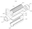
도 1은 예시적인 실시예에 따른 광원 모듈을 개략적으로 나타내는 분해사시도이다.
도 2는 도 1의 광원 모듈을 개략적으로 나타내는 단면도이다.
도 3은 도 2의 평면도이다.
도 4a 및 도 4b는 각각 본 발명의 예시적 실시예들에 따른 패턴의 모양을 개략적으로 나타내는 평면도이다.
도 5a 및 도 5b는 각각 본 발명의 다른 예시적 실시예들에 따른 패턴의 모양을 개략적으로 나타내는 평면도이다.
도 6은 본 발명의 예시적 실시예에 따른 광원 모듈을 개략적으로 나타내는 단면도이다.
도 7은 본 발명의 예시적 실시예에 따른 광원 모듈을 개략적으로 나타내는 단면도이다.
도 8은 본 발명의 예시적 실시예에 따른 광원을 개략적으로 나타내는 단면도이다.
도 9a 및 도 9b는 본 발명의 예시적 실시예에 따른 광원을 개략적으로 나타내는 단면도이다.
도 10은 본 발명에 채용가능한 파장변환물질을 설명하기 위한 CIE1931 좌표계이다.
도 11a는 본 발명에 채용될 수 있는 LED 칩의 일 예를 나타내는 평면도이다.
도 11b는 도 11a에 도시된 LED 칩을 I-I'선으로 절취한 단면도이다.
도 12는 본 발명에 채용될 수 있는 LED 칩의 일 예를 나타내는 단면도이다.
도 13은 예시적인 실시예들에 따른 광원 모듈을 채용할 수 있는 조명 장치를 개략적으로 나타내는 단면도이다.
도 14는 예시적인 실시예들에 따른 광원 모듈을 채용한 바(bar) 타입의 램프의 분해 사시도이다.
도 15는 예시적인 실시예들에 따른 광원 모듈을 채용할 수 있는 실내용 조명제어 네트워크 시스템이다.
도 16은 예시적인 실시예들에 따른 광원 모듈을 채용할 수 있는 개방형 네트워크 시스템이다.
도 17은 예시적인 실시예들에 따른 광원 모듈을 채용할 수 있는 가시광 무선 통신에 의한 조명 기구의 스마트 엔진과 모바일 기기의 통신 동작을 설명하기 위한 블록도이다.1 is an exploded perspective view schematically showing a light source module according to an exemplary embodiment.
2 is a cross-sectional view schematically showing the light source module of FIG.
3 is a plan view of Fig.
4A and 4B are plan views schematically illustrating the shape of a pattern according to exemplary embodiments of the present invention.
5A and 5B are plan views schematically illustrating the shape of a pattern according to another exemplary embodiment of the present invention.
6 is a cross-sectional view schematically showing a light source module according to an exemplary embodiment of the present invention.
7 is a cross-sectional view schematically showing a light source module according to an exemplary embodiment of the present invention.
8 is a cross-sectional view schematically illustrating a light source according to an exemplary embodiment of the present invention.
9A and 9B are cross-sectional views schematically illustrating a light source according to an exemplary embodiment of the present invention.
10 is a CIE 1931 coordinate system for explaining the wavelength conversion material usable in the present invention.
11A is a plan view showing an example of an LED chip that can be employed in the present invention.
11B is a cross-sectional view taken along line I-I 'of the LED chip shown in FIG. 11A.
12 is a cross-sectional view showing an example of an LED chip that can be employed in the present invention.
13 is a cross-sectional view schematically showing a lighting device capable of employing a light source module according to exemplary embodiments.
14 is an exploded perspective view of a bar-type lamp employing a light source module according to exemplary embodiments.
15 is an interior lighting control network system capable of employing a light source module according to exemplary embodiments.
16 is an open network system capable of employing a light source module according to exemplary embodiments.
17 is a block diagram for explaining a communication operation between a smart engine and a mobile device of a lighting device by visible light wireless communication capable of employing a light source module according to exemplary embodiments.
이하, 첨부된 도면을 참조하여 본 발명의 바람직한 실시 형태들을 설명한다. 그러나, 본 발명의 실시형태는 여러 가지 다른 형태로 변형될 수 있으며, 본 발명의 범위가 이하 설명하는 실시 형태로 한정되는 것은 아니다.Hereinafter, preferred embodiments of the present invention will be described with reference to the accompanying drawings. However, the embodiments of the present invention can be modified into various other forms, and the scope of the present invention is not limited to the embodiments described below.
또한, 본 발명의 실시형태는 당해 기술분야에서 평균적인 지식을 가진 자에게 본 발명을 더욱 완전하게 설명하기 위해서 제공되는 것이다. 따라서, 도면에서 요소들의 형상 및 크기 등은 보다 명확한 설명을 위해 과장될 수 있으며, 도면 상의 동일한 부호로 표시되는 요소는 동일한 요소이다. 본 명세서에서, '상', '상부', '상면', '하', '하부', '하면', '측면' 등의 용어는 도면을 기준으로 한 것이며, 실제로는 소자나 구성요소가 배치되는 방향에 따라 달라질 수 있을 것이다.
Further, the embodiments of the present invention are provided to more fully explain the present invention to those skilled in the art. Accordingly, the shapes and sizes of the elements in the drawings may be exaggerated for clarity of description, and the elements denoted by the same reference numerals in the drawings are the same elements. In this specification, terms such as "upper,""upper,""upper,""lower,""lower,""lower,""side," and the like are based on the drawings, It will be possible to change depending on the direction.
도 1 내지 도 3을 참조하여 본 발명의 예시적 실시예에 따른 광원 모듈을 설명한다. 도 1은 예시적인 실시예에 따른 광원 모듈을 개략적으로 나타내는 분해사시도이고, 도 2는 도 1의 광원 모듈을 개략적으로 나타내는 단면도이고, 도 3은 도 2의 평면도이다.
1 to 3, a light source module according to an exemplary embodiment of the present invention will be described. FIG. 1 is an exploded perspective view schematically showing a light source module according to an exemplary embodiment, FIG. 2 is a sectional view schematically showing the light source module of FIG. 1, and FIG. 3 is a plan view of FIG.
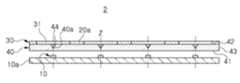
도 1 내지 도 3을 참조하면, 본 발명의 일 실시형태에 따른 광원 모듈(1)은 광원(10), 상기 광원(10) 상에 배치되는 도광판(20) 및 상기 도광판(20)의 상면에 부착되는 필터 시트(30)를 포함할 수 있다.
1 to 3, a
상기 광원(10)은 외부에서 인가되는 구동 전원에 의해 소정 파장의 광을 발생시키는 광전소자(Optoelectronic Device)일 수 있다. 예를 들어, n형 반도체층 및 p형 반도체층과 이들 사이에 배치된 활성층을 갖는 반도체 발광다이오드(LED)를 포함할 수 있다.The
상기 광원(10)은 청색 광, 녹색 광 또는 적색 광을 발광할 수 있으며, 자외 광 등을 발광할 수도 있다. 필요에 따라 형광체와 같은 파장변환물질과 결합하여 백색 광을 방출할 수 있다.
The
상기 광원(10)은 기판(10a) 상에 장착되어 전기적으로 연결될 수 있다. 상기 광원(10)은 복수개가 상기 기판(10a) 상에 횡 방향 및 종 방향을 따라서 각각 복수의 열을 이루며 배열될 수 있다.The
상기 기판(10a)은 인쇄회로기판일 수 있다. 예를 들어, FR4 타입의 인쇄회로기판(PCB) 혹은 변형이 쉬운 플렉서블(flexible) 인쇄회로기판일 수 있다. 이러한 인쇄회로기판은 에폭시, 트리아진, 실리콘, 및 폴리이미드 등을 함유하는 유기 수지 소재 및 기타 유기 수지 소재로 형성되거나, 실리콘 나이트라이드, AlN, Al2O3 등의 세라믹 소재로 형성되거나, MCPCB, MCCL 등과 같이 금속 및 금속화합물로 형성될 수 있다.
The
상기 도광판(20)은 상기 광원(10)을 덮는 형태로 상기 광원(10) 상에 배치될 수 있다. 상기 도광판(20)은 상기 광원(10)과 마주하는 제1면(21)과, 상기 제1면(21)과 반대에 배치되는 제2면(22)과, 상기 제1면(21)과 제2면(22) 사이의 제3면(23)을 포함할 수 있다.
The
상기 제1면(21)은 상기 도광판(20)의 바닥면에 해당되며, 상기 광원(10)의 광은 상기 제1면(21)을 통해서 상기 도광판(20) 내부로 입사될 수 있다. 상기 제2면(22)은 상기 도광판(20)의 상면에 해당되며, 상기 도광판(20)의 내부로 입사된 광은 상기 제2면(22)을 통해서 외부로 방출될 수 있다. 상기 제3면(23)은 상기 도광판(20)의 측면에 해당되며, 상기 제1면(21)의 가장자리와 상기 제2면(22)의 가장자리를 상호 연결할 수 있다.
The
상기 도광판(20)은 상면인 상기 제2면(22)에 홈부(20a)를 가질 수 있다. 상기 홈부(20a)는 상기 제2면(22)에서 상기 광원(10)을 향해 소정 깊이로 함몰된 구조를 가질 수 있다. 상기 홈부(20a)는, 예를 들어, 원뿔, 삼각뿔, 사각뿔 등의 형상을 가질 수 있다.The
상기 홈부(20a)는 상기 광원(10)과 마주하여 위치하며, 상기 광원(10)을 향해 함몰된 꼭짓점이 상기 광원(10)의 광축(Z)에 놓일 수 있다. 상기 홈부(20a)는 적어도 상기 광원(10)과 대응되는 갯수로 구비될 수 있다.The
상기 홈부(20a)는 상기 광원(10)의 광을 굴절 및 반사시켜서 상기 광축(Z)에 대해 측방향으로 넓게 상기 도광판(20)의 내부를 따라서 확산되도록 한다. 이를 통해서 상기 광원(10)에서 출사되는 광이 상기 광원(10)의 상부에 집중되어 휘도 불균일에 따른 핫스팟(hot spot)이 발생하는 것을 완화하거나 방지할 수 있다.
The
또한, 상기 도광판(20) 내부로 입사하여 전반사되고 있는 광이 상기 제2면(22)을 통해서 외부로 방출되도록 상기 제1면(21)에 요철무늬(hole, bump 등)를 가지거나 패터닝된 반사면을 가질 수 있으며, 혹은 상면인 상기 제2면(22)에 요철무늬를 가질 수 있다.
A hole or bump is formed on the
상기 도광판(20)은 투광성 재질로 형성될 수 있다. 상기 재질로는, 예를 들어, 폴리카보네이트(polycarbonate, PC), 폴리메틸메타크릴레이트(PMMA), 아크릴(acryl), 레진 등을 포함할 수 있다. 또한, 글라스 재질로 이루어질 수도 있으나, 이에 한정하는 것은 아니다.
The
상기 도광판(20)은 대략 2mm 내지 5mm 사이의 범위에 해당하는 두께를 가질 수 있다. 이와 같이 도광판(20)이 얇은 두께를 가짐으로써 전체적인 광원 모듈(1)의 슬림화 구현이 가능하다.
The
상기 필터 시트(30)는 상기 도광판(20)의 제2면(22)에 부착되어 상기 도광판(20)의 상면을 덮을 수 있다. 상기 필터 시트(30)는 박막 형태로 상기 도광판(20)에 부착되거나 스크린 프린팅과 같은 프린팅 방법을 통해서 프린팅되어 상기 도광판(20)의 상면을 덮을 수 있다. 상기 필터 시트(30)는 상기 도광판(20)의 상면 전체를 덮을 수 있고, 혹은 상면 중 홈부(20a) 영역에만 덮을 수 있다.The
상기 필터 시트(30)는 패턴(31)을 가지며, 상기 광원(10)의 광을 부분적으로 투과시키고 부분적으로 반사시킬 수 있다.
The
상기 패턴(31)은 상기 홈부(20a) 상에 배치되어 상기 홈부(20a)를 덮을 수 있다. 상기 패턴(31)은 상기 제2면(22)으로 노출되는 상기 홈부(20a)보다 큰 사이즈를 가져 상기 홈부(20a)를 포함하여 상기 홈부(20a) 주위의 일정 영역을 덮을 수 있다.The
본 실시 형태에서는 상기 패턴(31)이 전체적으로 원형의 모양을 가지는 것으로 예시하고 있으나 이에 한정하는 것은 아니다. 예를 들어, 상기 패턴(31)은 삼각형, 사각형, 육각형, 팔각형 등의 기타 다양한 모양을 가지는 것도 가능하다.
In the present embodiment, the
도 4a에서는 상기 패턴의 일 실시예를 개략적으로 나타내고 있다. 도 4a는 본 발명의 예시적 실시예들에 따른 패턴의 모양을 개략적으로 나타내는 평면도이다.4A schematically shows an embodiment of the pattern. 4A is a plan view schematically illustrating the shape of a pattern according to exemplary embodiments of the present invention.
도 4a를 참조하면, 상기 패턴(31)은 반사 물질을 포함하는 복수의 도트(31a)가 방사상으로 배열된 구조를 가질 수 있다. 즉, 상기 복수의 도트(31a)가 모여서 상기 패턴(31)을 이룰 수 있다.Referring to FIG. 4A, the
상기 복수의 도트(31a)는 배열되는 영역에 따라서 서로 다른 크기를 가질 수 있다. 구체적으로, 상기 복수의 도트(31a)는 상기 홈부(20a)의 중앙을 기준으로 상기 중앙에서 멀어질수록 크기가 작아질 수 있다. 즉, 상기 광원(10)의 직상부에 해당하는 상기 패턴(31)의 중심부에 배열되는 도트(31a)의 크기가 가장 크고, 상기 패턴(31)의 가장자리로 갈수록 상기 도트(31a)의 크기는 작아져 상기 패턴(31)의 가장자리에 배열되는 도트(31a)의 크기가 가장 작을 수 있다.The plurality of
또한, 상기 패턴(31)의 중심부에서 가장자리로 갈수록 상기 복수의 도트(31a) 사이의 간격은 커질 수 있다. 즉, 상기 홈부(20a)의 중앙에서 멀어질수록 도트(31a) 사이의 간격은 증가될 수 있다.In addition, the distance between the
따라서, 상기 패턴(31)은 중심부에서 상기 복수의 도트(31a)가 가장 높은 밀도로 배열되고, 상기 패턴(31)의 가장자리로 갈수록 밀도가 작아지는 구조로 배열되는 구조를 가질 수 있다.
Accordingly, the
본 실시 형태에서 상기 각 도트(31a)는 원형의 모양을 가지는 것으로 예시하고 있으나, 이에 한정하는 것은 아니다. 예를 들어, 상기 도트(31a)는 사각형, 육각형, 팔각형 등의 다양한 모양을 가지는 것도 가능하다.
In the present embodiment, each of the
상기 도트(31a)를 이루는 반사 물질로는, 예를 들어, SiO2, TiO2 및 Al2O3로 구성된 그룹으로부터 선택된 하나 이상의 물질을 포함할 수 있다. 또한, 알루미늄(Al)과 같은 금속 물질을 포함할 수 있다.
A reflective material of the dots (31a) is, for example, may include one or more materials selected from the group consisting of SiO2, TiO2 and Al2 O3. Further, it may include a metal material such as aluminum (Al).
상기 복수의 도트(31a)가 배열되어 이루어지는 상기 패턴(31)은 상기 광원(10)과 홈부(20a)의 위치에 대응하여 상기 홈부(20a)를 충분히 덮을 수 있도록 배치되며, 상기 홈부(20a)에 의해 반사되지 못하고 상기 도광판(20)의 상부로 그대로 방출되는 광을 부분적으로 반사시켜서 상기 도광판(20)의 내부로 재입사되도록 할 수 있다.The
상기 패턴(31)에 의해 반사되어 상기 도광판(20)으로 재입사된 광은 상기 도광판(20)의 하면인 제1면(21)에서 재반사되어 상기 제2면(22)을 통과하여 외부로 방출될 수 있다.
The light reflected by the
상기 광원(10)의 광은 상기 도광판(20)을 통해서 면광원 형태로 외부로 방출될 수 있으며, 본 실시 형태에서는 상기 광원(10)의 상부에 패턴(31)을 배치함으로써 상기 광원(10)의 상부에 광이 집중되어 핫스팟이 발생하는 것을 방지할 수 있다.The light of the
특히, 본 실시 형태에서는 상기 패턴(31)을 이루는 복수의 도트(31a)가 서로 다른 크기와 간격으로 배열되되, 상기 광원(10)의 직상부에 해당하는 영역에는 높은 밀도로 배열되고 가장자리로 갈수록 낮은 밀도로 배열되도록 하는데 특징이 있다. 이를 통해서 광이 상기 패턴(31)을 부분적으로 투과하고 부분적으로 반사되도록 하되, 중심부에서는 상대적으로 투과율이 낮아지고 가장자리 부분에서는 상대적으로 투과율이 높아지도록 하여 전체적인 휘도 분포의 균일도를 향상시킬 수 있다.
Particularly, in the present embodiment, a plurality of
도 4b에서는 상기 패턴의 다른 실시예를 개략적으로 나타내고 있다. 도 4b는 본 발명의 예시적 실시예들에 따른 패턴의 모양을 개략적으로 나타내는 평면도이다.FIG. 4B schematically shows another embodiment of the pattern. 4B is a plan view schematically illustrating the shape of a pattern according to exemplary embodiments of the present invention.
도 4b를 참조하면, 상기 패턴(32)은 상기 도광판(20)의 상면 중 적어도 일부를 노출시키는 복수의 홀(32a)이 방사상으로 배열된 구조를 가질 수 있다. 즉, 상기 패턴(32)은 방사상으로 배열된 상기 복수의 홀(32a)을 포함할 수 있다.
Referring to FIG. 4B, the
상기 복수의 홀(32a)은 배열되는 영역에 따라서 서로 다른 크기를 가질 수 있다. 구체적으로, 상기 복수의 홀(32a)은 상기 홈부(20a)의 중심을 기준으로 상기 중심에서 멀어질수록 크기가 커질 수 있다. 즉, 상기 광원(10)의 직상부에 해당하는 상기 패턴(32)의 중심부에 배열되는 홀(32a)의 크기가 가장 작고, 상기 패턴(32)의 가장자리로 갈수록 상기 홀(32a)의 크기는 커져 상기 패턴(32)의 가장자리에 배열되는 홀(32a)의 크기가 가장 클 수 있다.The plurality of
또한, 상기 패턴(32)의 중심부에서 가장자리로 갈수록(상기 홈부에서 멀어질수록) 상기 복수의 홀(32a) 사이의 간격은 작아질 수 있다.Further, the distance between the center of the
따라서, 상기 패턴(32)은 중심부에서 상기 복수의 홀(32a)이 가장 작은 밀도로 배열되고, 상기 패턴(32)의 가장자리로 갈수록 밀도가 커지는 구조로 배열되는 구조를 가질 수 있다.
Therefore, the
본 실시 형태에서 상기 각 홀(32a)은 원형의 모양을 가지는 것으로 예시하고 있으나, 이에 한정하는 것은 아니다. 예를 들어, 상기 홀(32a)은 사각형, 육각형, 팔각형 등의 다양한 모양을 가지는 것도 가능하다.
In the present embodiment, each of the
도 4a에 도시된 실시 형태에 따른 패턴(31)과 달리 본 실시 형태에서는 상기 패턴(32)을 이루는 복수의 홀(32a)이 서로 다른 크기와 간격으로 배열되되, 상기 광원(10)의 직상부에 해당하는 영역에는 낮은 밀도로 배열되고 가장자리로 갈수록 높은 밀도로 배열될 수 있다. 이를 통해서 광이 상기 패턴(32)을 부분적으로 투과하고 부분적으로 반사되도록 하되, 중심부에서는 투과율이 낮고 가장자리 부분에서는 투과율이 높아지도록 하여 전체적인 휘도 분포의 균일도를 향상시킬 수 있다.
4A, the plurality of
도 5a 및 도 5b에서는 상기 패턴의 다른 실시예를 개략적으로 나타내고 있다.5A and 5B schematically show another embodiment of the pattern.
도 5a 및 도 5b를 참조하면, 상기 패턴(33)은 반사 물질로 이루어진 막대 형상을 갖는 복수의 줄기(33a)가 방사상으로 연장된 별 모양의 구조를 가질 수 있다. 상기 줄기(33a)는 직선 모양을 가질 수 있다. 또한, 도 5b에서와 같이 상기 줄기(33b)는 삼각형의 모양을 가질 수 있다.
5A and 5B, the
도 6을 참조하여 본 발명의 예시적 실시예에 따른 광원 모듈을 설명한다. 도 6은 예시적인 실시예에 따른 광원 모듈을 개략적으로 나타내는 단면도이다.The light source module according to the exemplary embodiment of the present invention will be described with reference to FIG. 6 is a cross-sectional view schematically showing a light source module according to an exemplary embodiment.
도 6을 참조하면, 본 발명의 예시적 실시예에 따른 광원 모듈(2)은 광원(10), 상기 광원(10) 상에 배치되는 도광판(40) 및 상기 도광판(40)의 상면에 부착되는 필터 시트(30)를 포함할 수 있다.
6, the
도 6에서 도시하는 실시예에 따른 수지 광원 모듈(2)을 구성하는 구성은 상기 도 1 내지 도 5에 도시된 실시예에 따른 광원 모듈(1)과 기본적인 구성이 실질적으로 동일하다. 다만, 도광판(40)과 관련하여 광확산부(44)를 포함하는 점에서 상기 도 1 내지 도 5에 도시된 실시예와 다르기 때문에 이하에서는 앞서 설명한 실시예와 중복되는 부분에 관한 설명은 생략하고 차이점을 위주로 설명한다.
The configuration of the resin
도 6을 참조하면, 상기 도광판(40)은 광원(10)과 마주하는 제1면(41)과, 상기 제1면(41)과 반대에 배치되는 제2면(42)과, 상기 제1면(41)과 제2면(42) 사이의 제3면(43)을 포함할 수 있다.6, the
상기 제1면(41)은 상기 도광판(40)의 바닥면에 해당되며, 상기 광원(10)의 광은 상기 제1면(41)을 통해서 상기 도광판(40) 내부로 입사될 수 있다. 상기 제2면(42)은 상기 도광판(40)의 상면에 해당되며, 상기 도광판(40)의 내부로 입사된 광은 상기 제2면(42)을 통해서 외부로 방출될 수 있다. 상기 제3면(43)은 상기 도광판(40)의 측면에 해당되며, 상기 제1면(41)의 가장자리와 상기 제2면(42)의 가장자리를 상호 연결할 수 있다.
The first surface 41 corresponds to the bottom surface of the
상기 도광판(40)은 상면인 상기 제2면(42)에 홈부(40a)를 가질 수 있다. 상기 홈부(40a)는 상기 제2면(42)에서 상기 광원(10)을 향해 소정 깊이로 함몰된 구조를 가질 수 있다. 상기 홈부(40a)는 상기 광원(10)과 마주하여 위치하며, 상기 광원(10)을 향해 함몰된 꼭짓점이 상기 광원(10)의 광축(Z)에 놓일 수 있다.
The
상기 도광판(40)은 상기 홈부(40a)를 채우는 광확산부(44)를 포함할 수 있다. 상기 광확산부(44)는, 예를 들어, 투광성을 갖는 레진에 광확산물질로 SiO2, TiO2 및 Al2O3로 구성된 그룹으로부터 선택된 하나 이상의 물질을 함유할 수 있다.The
상기 광확산부(44)가 상기 홈부(40a)를 채우는 구조로 구비됨으로써 상기 도광판(40)은 제2면(42)이 상기 제1면(41)과 같이 평평한 구조를 가질 수 있다.
The
상기 광확산부(44)는 상기 홈부(40a)와의 계면에서 반사되지 않고 굴절되어 상기 광확산부(44)로 입사된 광을 반사 및 분산시켜서 다시 상기 도광판(40)의 내부로 확산되도록 할 수 있다. 따라서, 상기 홈부(40a)가 비어있는 구조에 비해 상기 광원(10)의 광이 보다 넓게 도광판(40)의 내부로 확산되도록 할 수 있다.
The
도 7을 참조하여 본 발명의 예시적 실시예에 따른 광원 모듈을 설명한다. 도 7은 예시적인 실시예에 따른 광원 모듈을 개략적으로 나타내는 단면도이다.A light source module according to an exemplary embodiment of the present invention will be described with reference to FIG. 7 is a cross-sectional view schematically showing a light source module according to an exemplary embodiment.
도 7을 참조하면, 본 발명의 예시적 실시예에 따른 광원 모듈(3)은 광원(10), 상기 광원(10) 상에 배치되는 도광판(50) 및 상기 도광판(50)의 상면에 부착되는 필터 시트(30)를 포함할 수 있다.
7, the
도 7에서 도시하는 실시예에 따른 수지 광원 모듈(3)을 구성하는 구성은 상기 도 1 내지 도 5에 도시된 실시예에 따른 광원 모듈(1)과 기본적인 구성이 실질적으로 동일하다. 다만, 도광판(50)과 관련하여 수용홈(50b)을 포함하는 점에서 상기 도 1 내지 도 5에 도시된 실시예와 다르기 때문에 이하에서는 앞서 설명한 실시예와 중복되는 부분에 관한 설명은 생략하고 차이점을 위주로 설명한다.
The configuration of the resin
도 7을 참조하면, 상기 도광판(50)은 제1면(51)과, 상기 제1면(51)과 반대에 배치되는 제2면(52)과, 상기 제1면(51)과 제2면(52) 사이의 제3면(53)을 포함할 수 있다.7, the
상기 제1면(51)은 상기 도광판(50)의 바닥면에 해당되며, 상기 광원(10)의 광은 상기 제1면(51)을 통해서 상기 도광판(50) 내부로 입사될 수 있다. 상기 제2면(52)은 상기 도광판(50)의 상면에 해당되며, 상기 도광판(50)의 내부로 입사된 광은 상기 제2면(52)을 통해서 외부로 방출될 수 있다. 상기 제3면(53)은 상기 도광판(50)의 측면에 해당되며, 상기 제1면(51)의 가장자리와 상기 제2면(52)의 가장자리를 상호 연결할 수 있다.
The
상기 도광판(50)은 상면인 상기 제2면(52)에 홈부(50a)를 가질 수 있다. 상기 홈부(50a)는 상기 제2면(52)에서 상기 광원(10)을 향해 소정 깊이로 함몰된 구조를 가질 수 있다. 상기 홈부(50a)는 상기 광원(10)과 마주하여 위치하며, 상기 광원(10)을 향해 함몰된 꼭짓점이 상기 광원(10)의 광축(Z)에 놓일 수 있다.
The
상기 도광판(50)은 하면인 상기 제1면(51)에 수용홈(50b)을 가질 수 있다. 상기 수용홈(50b)은 상기 제1면(51)에서 상기 제2면(52)을 향해 소정 깊이로 함몰된 구조를 가질 수 있다. 상기 수용홈(50b)은 상기 홈부(50a)와 마주하여 위치하며, 상기 광원(10)을 내부에 수용할 수 있다.
The
상기 수용홈(50b)은 반원 또는 반타원 모양의 돔 형상을 가질 수 있으며, 상기 광원(10)을 내부에 수용할 수 있는 크기를 가질 수 있다. 상기 수용홈(50b)의 표면은 상기 광원(10)의 광이 상기 도광판(50)의 내부로 입사되는 입사면을 정의할 수 있다.The receiving
이와 같이 수용홈(50b)이 돔 형상을 가짐으로써 상기 도광판(50)의 내부로 입사되는 광은 보다 넓은 영역으로 확산될 수 있다.
Since the receiving
본 실시 형태에 따른 광원 모듈(1)에는 다양한 형태의 광원(10)이 채용될 수 있다. 이러한 광원(10)은 다양한 구조의 발광다이오드(LED) 칩 또는 상기 발광다이오드 칩이 장착된 발광다이오드 패키지가 사용될 수 있다.
Various types of
도 8에서는 본 발명의 예시적 실시예에 따른 광원(10)을 개략적으로 나타내고 있다. 도 8에서 도시하는 바와 같이 상기 광원(10)은, 예를 들어, 반사컵(13)을 갖는 패키지 몸체(12) 내에 LED 칩(11)이 실장된 패키지 구조를 가질 수 있다. 그리고, LED 칩(11)은 형광체를 함유하는 봉지부(14)에 의해 커버될 수 있다.
8 schematically shows a
상기 패키지 몸체(12)는 상기 LED 칩(11)이 실장되어 지지되는 베이스 부재에 해당하며, 광 반사율이 높은 백색 성형 복합재(molding compound)로 이루어질 수 있다. 이는 LED 칩(11)에서 방출되는 광을 반사시켜 외부로 방출되는 광량을 증가시키는 효과가 있다. 이러한 백색 성형 복합재는 고 내열성의 열경화성 수지 계열 또는 실리콘 수지 계열을 포함할 수 있다. 또한, 열 가소성 수지 계열에 백색 안료 및 충진제, 경화제, 이형제, 산화방지제, 접착력 향상제 등이 첨가될 수 있다. 또한, FR-4, CEM-3, 에폭시 재질 또는 세라믹 재질 등으로도 이루어질 수 있다. 또한, 알루미늄(Al)과 같은 금속 재질로 이루어지는 것도 가능하다.
The
상기 패키지 몸체(12)에는 외부 전원과의 전기적 연결을 위한 리드 프레임(15)이 구비될 수 있다. 상기 리드 프레임(15)은 전기 전도성이 우수한 재질, 예를 들어, 알루미늄, 구리 등의 금속 재질로 이루어질 수 있다. 만일, 상기 패키지 몸체(12)가 금속 재질로 이루어지는 경우에는 상기 패키지 몸체(12)와 상기 리드 프레임(15) 사이에는 절연 물질이 개재될 수 있다.
The
상기 패키지 몸체(12)에 구비되는 상기 반사컵(13)에는 상기 LED 칩(11)이 실장되는 바닥면으로 상기 리드 프레임(15)이 노출될 수 있다. 그리고, 상기 LED 칩(11)은 상기 노출된 리드 프레임(15)과 전기적으로 접속될 수 있다.The
상기 반사컵(13)의 상기 패키지 몸체(12)의 상면으로 노출되는 단면의 크기는 상기 반사컵(13)의 바닥면의 크기보다 큰 구조를 가질 수 있다. 여기서, 상기 반사컵(13)의 상기 패키지 몸체(12)의 상면으로 노출되는 단면은 상기 광원(10)의 발광면을 정의할 수 있다.
The size of the cross section of the
상기 LED 칩(11)은 상기 패키지 몸체(12)의 반사컵(13) 내에 형성되는 봉지부(14)에 의해 밀봉될 수 있다. 상기 봉지부(14)에는 파장변환물질이 함유될 수 있다.
The
도 9a 및 도 9b에서는 본 발명의 예시적 실시예에 따른 광원(10')을 개략적으로 나타내고 있다.9A and 9B schematically illustrate a light source 10 'according to an exemplary embodiment of the present invention.
도 9a에서 도시하는 바와 같이 상기 광원(10')은, 예를 들어, LED 칩(11)이 파장변환층(16)에 의해 봉지된 POC(Phosphor on Chip) 구조를 가질 수 있다. 상기 파장변환층(16)은 전체적으로 균일한 두께를 가지며 상기 LED 칩(11)의 표면을 덮을 수 있다. 또한, 도 9b에서 도시하는 바와 같이, 파장변환층(17)은 돔 형태로 상기 LED 칩(11)을 봉지할 수 있다.As shown in FIG. 9A, the light source 10 'may have a POC (Phosphor on Chip) structure in which the
이와 같이, 광원(10')이 POC 구조를 가지는 경우 도 8에서 도시하는 패키지 구조를 갖는 광원(10)에 비해 보다 넓은 지향각 특성을 가질 수 있다.
As described above, when the light source 10 'has a POC structure, it can have a wider orientation angle characteristic than the
상기 LED 칩(11)은, 예를 들어, 솔더와 같은 접합 부재를 통해서 상기 기판(10a) 상에 플립칩 본딩 방식으로 장착될 수 있다.The
상기 파장변환층(16,17)은 상기 LED 칩(11)을 전체적으로 봉지하여 상기 LED 칩(11)의 상면과 측면을 일체로 덮을 수 있다. 상기 파장변환층(16, 17)은, 예를 들어, 투광성을 갖는 수지와, 상기 수지 내에 함유되는 파장변환물질을 포함할 수 있다.
The wavelength conversion layers 16 and 17 may encapsulate the
상기 파장변환물질로는, 예컨대 상기 LED 칩(11)에서 발생된 광에 의해 여기되어 다른 파장의 광을 방출하는 형광체가 적어도 1종 이상 함유될 수 있다. 이를 통해 백색 광을 비롯해 다양한 색상의 광이 방출될 수 있도록 조절할 수 있다.As the wavelength converting material, for example, at least one fluorescent material that is excited by the light emitted from the
예를 들어, LED 칩(11)이 청색 광을 발광하는 경우, 황색, 녹색, 적색 및/또는 오랜지색의 형광체를 조합하여 백색 광을 발광하도록 할 수 있다. 또한, 보라색, 청색, 녹색, 적색 또는 적외선을 발광하는 LED 칩 중 적어도 하나를 포함하게 구성할 수도 있다. 이 경우, 상기 LED 칩(11)은 연색성(CRI)을 '40'에서 '100' 수준으로 조절할 수 있으며, 또한, 색온도를 대략 2000K에서 20000K 수준으로 다양한 백색 광을 발생시킬 수 있다. 또한, 필요에 따라서는 보라색, 청색, 녹색, 적색, 오랜지색의 가시광 또는 적외선을 발생시켜 주위 분위기 또는 기분에 맞게 색을 조정할 수 있다. 또한, 식물 성장을 촉진할 수 있는 특수 파장의 광을 발생시킬 수도 있다.
For example, when the
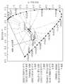
청색 LED 칩에 황색, 녹색, 적색 형광체 및/또는 녹색 LED 칩과 적색 LED 칩의 조합으로 만들어지는 백색 광은 2개 이상의 피크 파장을 가지며, 도 10에서 도시하는 CIE 1931 좌표계의 (x, y) 좌표가 (0.4476, 0.4074), (0.3484, 0.3516), (0.3101, 0.3162), (0.3128, 0.3292), (0.3333, 0.3333)을 잇는 선분 상에 위치할 수 있다. 또는, 상기 선분과 흑체 복사 스펙트럼으로 둘러싸인 영역에 위치할 수 있다. 상기 백색 광의 색 온도는 대략 2000K ~ 20000K사이에 해당한다.(X, y) of the CIE 1931 coordinate system shown in FIG. 10 has a peak wavelength of 2 or more, and a white light made of a combination of yellow, green, red phosphor and / or a green LED chip and a red LED chip on the blue LED chip has two or more peak wavelengths. The coordinates can be located on a line segment connecting (0.4476, 0.4074), (0.3484, 0.3516), (0.3101, 0.3162), (0.3128, 0.3292), (0.3333, 0.3333). Alternatively, it may be located in an area surrounded by the line segment and the blackbody radiation spectrum. The color temperature of the white light corresponds to approximately between 2000K and 20000K.
도 10에서 상기 흑체 복사 스펙트럼 하부에 있는 점 E(0.3333, 0.3333) 부근의 백색 광은 상대적으로 황색계열 성분의 광이 약해진 상태로 사람이 육안으로 느끼기에는 보다 선명한 느낌 또는 신선한 느낌을 가질 수 있는 영역의 조명 광원으로 사용될 수 있다. 따라서, 상기 흑체 복사 스펙트럼 하부에 있는 점 E(0.3333, 0.3333) 부근의 백색 광을 이용한 조명 제품은 식료품, 의류 등을 판매하는 상가용 조명으로 효과가 좋다.
In FIG. 10, the white light near the point E (0.3333, 0.3333) under the black body radiation spectrum is a region in which the light of the yellowish component is relatively weak, Can be used as an illumination light source. Accordingly, the lighting product using white light near the point E (0.3333, 0.3333) located below the blackbody radiation spectrum is effective as a commercial lighting for selling foodstuffs, clothes, and the like.
형광체는 다음과 같은 조성식 및 컬러(color)를 가질 수 있다.The phosphor may have the following composition formula and color.
산화물계: 황색 및 녹색 Y3Al5O12:Ce, Tb3Al5O12:Ce, Lu3Al5O12:CeOxide system: yellow and green Y3 Al5 O12 : Ce, Tb3 Al5 O12 : Ce, Lu3 Al5 O12 : Ce
실리케이트계: 황색 및 녹색 (Ba,Sr)2SiO4:Eu, 황색 및 등색 (Ba,Sr)3SiO5:Ce(Ba, Sr)2 SiO4 : Eu, yellow and orange (Ba, Sr)3 SiO5 : Ce
질화물계: 녹색 β-SiAlON:Eu, 황색 La3Si6N11:Ce, 등색 α-SiAlON:Eu, 적색 CaAlSiN3:Eu, Sr2Si5N8:Eu, SrSiAl4N7:Eu, SrLiAl3N4:Eu, Ln4-x(EuzM1-z)xSi12-yAlyO3+x+yN18-x-y (0.5≤x≤3, 0<z<0.3, 0<y≤4) (단, 여기서 Ln은 IIIa 족 원소 및 희토류 원소로 이루어지는 군에서 선택되는 적어도 한 종의 원소이고, M은 Ca, Ba, Sr 및 Mg로 이루어지는 군에서 선택되는 적어도 한 종의 원소일 수 있다.)The nitride-based: the green β-SiAlON: Eu, yellowLa 3 Si 6 N 11: Ce , orange-colored α-SiAlON: Eu, redCaAlSiN 3: Eu, Sr 2 Si 5 N 8: Eu, SrSiAl 4 N 7: Eu, SrLiAl3 N 4: Eu, Ln 4 -x (Eu z M 1 -z) x Si 12- y
플루오라이트(fluoride)계: KSF계 적색 K2SiF6:Mn4+, K2TiF6:Mn4+, NaYF4:Mn4+, NaGdF4:Mn4+ , K3SiF7:Mn4+
Fluorite (fluoride) type: KSF-based RedK 2 SiF 6: Mn 4 + ,
형광체 조성은 기본적으로 화학양론(Stoichiometry)에 부합하여야 하며, 각 원소들은 주기율표상 각 족들 내 다른 원소로 치환이 가능하다. 예를 들어 Sr은 알카리토류(II)족의 Ba, Ca, Mg 등으로, Y는 란탄계열의 Tb, Lu, Sc, Gd 등으로 치환이 가능하다. 또한, 활성제인 Eu 등은 원하는 에너지 준위에 따라 Ce, Tb, Pr, Er, Yb 등으로 치환이 가능하며, 활성제 단독 또는 특성 변형을 위해 부활성제 등이 추가로 적용될 수 있다.The phosphor composition should basically conform to the stoichiometry, and each element can be replaced with another element in each group on the periodic table. For example, Sr can be substituted with Ba, Ca, Mg, etc. of the alkaline earth (II) group, and Y can be replaced with lanthanide series Tb, Lu, Sc, Gd and the like. In addition, Eu, which is an activator, can be substituted with Ce, Tb, Pr, Er, Yb or the like according to a desired energy level.
특히, 플루오라이트계 적색 형광체는 고온/고습에서의 신뢰성 향상을 위하여 각각 Mn을 함유하지 않는 불화물로 코팅되거나 형광체 표면 또는 Mn을 함유하지 않는 불화물 코팅 표면에 유기물 코팅을 더 포함할 수 있다. 상기와 같은 플루어라이트계 적색 형광체의 경우 기타 형광체와 달리 40nm 이하의 협반치폭을 구현할 수 있기 때문에, UHD TV와 같은 고해상도 TV에 활용될 수 있다.
In particular, the fluoride red phosphor may further include an organic coating on the fluoride coating surface or the fluoride coating surface that does not contain Mn, respectively, in order to improve the reliability at high temperature / high humidity. Unlike other phosphors, the fluorite red phosphor can be used in high-resolution TVs such as UHD TV because it can realize a narrower width of 40 nm or less.
또한, 파장변환물질은 형광체 대체 물질로 양자점(Quantum Dot, QD) 등의 물질들이 적용될 수 있으며, 형광체와 QD를 혼합 또는 QD 단독으로 사용될 수 있다.In addition, the wavelength conversion material may be a substitute material of a fluorescent material, such as a quantum dot (QD), or may be used as a QD alone or in combination with a fluorescent material.
QD는 III-V 또는 II-VI화합물 반도체를 이용하여 코어(Core)-쉘(Shell)구조를 가질 수 있다. 예를 들면, CdSe, InP 등과 같은 코어(core)와 ZnS, ZnSe과 같은 쉘(shell)을 가질 수 있다. 또한, 상기 QD는 코어 및 쉘의 안정화를 위한 리간드(ligand)를 포함할 수 있다. 예를 들어, 상기 코어 직경은 대략 1 ~ 30nm, 나아가 대략 3 ~ 10nm일 수 있다. 상기 쉘 두께는 대략 0.1 ~ 20nm, 나아가 0.5 ~ 2nm일 수 있다.QD can have a core-shell structure using III-V or II-VI compound semiconductors. For example, it may have a core such as CdSe, InP or the like and a shell such as ZnS or ZnSe. In addition, the QD may include a ligand for stabilizing the core and the shell. For example, the core diameter may be approximately 1 to 30 nm, further approximately 3 to 10 nm. The shell thickness may be approximately 0.1 to 20 nm, further 0.5 to 2 nm.
상기 양자점은 사이즈에 따라 다양한 컬러를 구현할 수 있으며, 특히 형광체 대체 물질로 사용되는 경우에는 적색 또는 녹색 형광체로 사용될 수 있다. 양자점을 이용하는 경우, 협반치폭(예, 약 35nm)을 구현할 수 있다.
The quantum dot can realize various colors depending on the size, and in particular, when used as a substitute for a phosphor, it can be used as a red or green phosphor. When a quantum dot is used, a narrow bandwidth (e.g., about 35 nm) can be realized.
이하에서는 본 발명에 따른 LED 칩의 다양한 실시예에 대해 설명한다. 도 11 및 도 12는 광원에 채용될 수 있는 LED 칩의 다양한 예를 나타내는 단면도이다.
Hereinafter, various embodiments of the LED chip according to the present invention will be described. 11 and 12 are sectional views showing various examples of LED chips that can be employed in a light source.
도 11a는 본 발명에 채용될 수 있는 LED 칩의 일 예를 나타내는 평면도이며, 도 11b는 도 11a에 도시된 LED 칩을 I-I'선으로 절취한 측단면도이다.FIG. 11A is a plan view showing an example of an LED chip that can be employed in the present invention, and FIG. 11B is a side sectional view taken along line I-I 'of the LED chip shown in FIG.
도 11a 및 도 11b에 도시된 LED 칩(100)은 조명용으로 고출력을 위한 대면적 구조일 수 있다. 상기 LED 칩(100)은 전류 분산의 효율 및 방열 효율을 높이기 위한 구조이다.The
상기 LED 칩(100)은 발광적층체(S)와, 제1 전극(120), 절연층(130), 제2 전극(108) 및 도전성 기판(110)을 포함할 수 있다. 상기 발광적층체(S)는 순차적으로 적층된 제1 도전형 반도체층(104), 활성층(105), 제2 도전형 반도체층(106)을 포함할 수 있다.
The
상기 제1 도전형 반도체층(104)은 n형 InxAlyGa1-x-yN (0≤x<1, 0≤y<1, 0≤x+y<1)을 만족하는 질화물 반도체일 수 있으며, n형 불순물은 Si일 수 있다. 예를 들어, 상기 제1 도전형 반도체층(104)은 n형 GaN을 포함할 수 있다.The first
상기 제2 도전형 반도체층(106)은 p형 InxAlyGa1-x-yN (0≤x<1, 0≤y<1, 0≤x+y<1)을 만족하는 질화물 반도체층일 수 있으며, p형 불순물은 Mg일 수 있다. 예를 들어, 상기 제2 도전형 반도체층(106)은 p형 GaN을 포함할 수 있다.The second conductivity
상기 활성층(105)은 양자우물층과 양자장벽층이 서로 교대로 적층된 다중 양자우물(MQW) 구조일 수 있다. 예를 들어, 상기 양자우물층과 양자장벽층은 서로 다른 조성을 갖는 InxAlyGa1-x-yN (0≤x≤1, 0≤y≤1, 0≤x+y≤1)일 수 있다. 특정 예에서, 상기 양자우물층은 InxGa1-xN (0<x≤1)이며, 상기 양자장벽층은 GaN 또는 AlGaN일 수 있다. 양자우물층과 양자장벽층의 두께는 각각 대략 1nm ~ 50nm 범위일 수 있다. 상기 활성층(105)은 다중양자우물구조에 한정되지 않고, 단일양자우물(SQW) 구조일 수 있다.
The
상기 제1 전극(120)은 제1 도전형 반도체층(104)에 전기적으로 접속하기 위하여 제2 도전형 반도체층(106) 및 활성층(105)과는 전기적으로 절연되어 상기 제1 도전형 반도체층(104)의 적어도 일부 영역까지 연장된 하나 이상의 도전성 비아(180)를 포함할 수 있다. 상기 도전성 비아(180)는 제1 전극(120)의 계면에서부터 제2 전극(108), 제2 도전형 반도체층(106) 및 활성층(105)을 통과하여 제1 도전형 반도체층(104) 내부까지 연장될 수 있다. 이러한 도전성 비아(180)는 식각 공정, 예를 들어, ICP-RIE 등을 이용하여 형성될 수 있다.The
상기 제1 전극(120) 상에는 상기 제1 전극(120)이 상기 제1 도전형 반도체층(104)을 제외한 다른 영역과 전기적으로 절연시키기 위한 절연층(130)이 제공된다. 도 9b에 도시된 바와 같이, 상기 절연층(130)은 상기 제2 전극(108)과 제1 전극(120)의 사이뿐만 아니라 상기 도전성 비아(180)의 측면에도 형성된다. 이로써, 상기 도전성 비아(180)의 측면에 노출되는 상기 제2 전극(108), 제2 도전형 반도체층(106) 및 활성층(105)과 상기 제1 전극(120)을 절연시킬 수 있다. 절연층(130)은 SiO2, SiOxNy, SixNy과 같은 절연 물질을 증착시켜 형성될 수 있다.
An insulating
상기 도전성 비아(180)에 의해 제1 도전형 반도체층(104)의 컨택영역(C)이 노출되며, 상기 제1 전극(120)의 일부 영역은 상기 도전성 비아(180)를 통해 상기 컨택영역(C)에 접하도록 형성될 수 있다. 이로써, 상기 제1 전극(120)은 상기 제1 도전형 반도체층(104)에 접속될 수 있다.A contact region C of the first conductivity
상기 도전성 비아(180)는 접촉 저항이 낮아지도록 개수, 형상, 피치, 제1 및 제2 도전형 반도체층(104, 106)과의 접촉 직경(또는 접촉 면적) 등이 적절히 조절될 수 있으며(도 11a 참조), 행과 열을 따라 다양한 형태로 배열됨으로써 전류 흐름이 개선될 수 있다. 컨택영역(C) 면적은 발광적층체(S)의 평면 면적의 대략 0.1% 내지 20%의 범위가 되도록 도전성 비아(180)의 개수 및 접촉 면적이 조절될 수 있다. 예를 들어 0.5% 내지 15%이며, 나아가, 1% 내지 10%일 수 있다. 상기 면적이 0.1%보다 작으면 전류 분산이 균일하지 않아 발광 특성이 떨어지며, 또한 20% 이상으로 전극 면적이 증가하면 상대적으로 발광 면적의 감소로 발광 특성 및 휘도가 감소하는 문제가 발생할 수 있다.The number, shape, pitch, contact diameter (or contact area) of the
상기 제1 도전형 반도체층(104)과 접촉하는 영역의 도전성 비아(180)의 반경은 예를 들어, 1㎛ 내지 50㎛의 범위일 수 있으며, 도전성 비아(180)의 개수는 발광적층체(S) 영역의 넓이에 따라, 발광적층체(S) 영역 당 1개 내지 48000개일 수 있다. 도전성 비아(180)는 발광적층체(S) 영역의 넓이에 따라 다르지만, 예를 들어 2개 내지 45000개이며, 나아가 5개 내지 40000개이며, 더 나아가 10개 내지 35000개일 수 있다. 각 도전성 비아(180) 간의 거리는 10㎛ 내지 1000㎛ 범위의 행과 열을 가지는 매트릭스 구조일 수 있으며, 예를 들어 50㎛ 내지 700㎛ 범위일 수 있으며, 나아가 100㎛ 내지 500㎛범위일 수 있고, 더 나아가 150㎛ 내지 400㎛범위 일 수 있다.The radius of the
각 도전성 비아(180) 간의 거리가 10㎛보다 작으면 비아의 개수가 증가하게 되고 상대적으로 발광면적이 줄어들어 발광 효율이 떨어지며, 거리가 1000㎛보다 커지면 전류 확산이 어려워 발광 효율이 떨어지는 문제점이 있을 수 있다. 도전성 비아의 깊이는 제2 도전형 반도체층(106) 및 활성층(105)의 두께에 따라 다르게 형성될 수 있고, 예컨대, 0.1㎛ 내지 5.0㎛의 범위일 수 있다.
If the distance between the respective
상기 제2 전극(108)은 도 9b에서 도시된 바와 같이 상기 발광적층체(S) 외부로 연장되어 노출된 전극형성영역(D)을 제공한다. 상기 전극형성영역(D)은 외부 전원을 상기 제2 전극(108)에 연결하기 위한 전극패드부(119)를 구비할 수 있다. 이러한 전극형성영역(D)을 1개로 예시되어 있으나, 필요에 따라 복수개로 구비할 수 있다. 상기 전극형성영역(D)은 도 11a에 도시된 바와 같이 발광면적을 최대화하기 위해서 상기 LED 칩(100)의 일측 모서리에 형성할 수 있다.The
본 실시예와 같이, 전극패드부(119) 주위에는 에칭스톱용 절연층(140)이 배치될 수 있다. 상기 에칭스톱용 절연층(140)은 발광적층체(S) 형성 후 그리고 제2 전극(108)형성 전에 전극형성영역(D)에 형성될 수 있으며, 전극형성영역(D)을 위한 에칭공정시에 에칭스톱으로 작용할 수 있다.The insulating
상기 제2 전극(108)은 상기 제2 도전형 반도체층(106)과 오믹컨택을 이루면서도 높은 반사율을 갖는 물질이 사용될 수 있다. 이러한 제2 전극(108)의 물질로는 앞서 예시된 반사전극물질이 사용될 수 있다.
The
도 12는 본 발명에 채용될 수 있는 LED 칩의 일 예를 나타내는 측단면도이다.12 is a side sectional view showing an example of an LED chip that can be employed in the present invention.
도 12를 참조하면, 상기 LED 칩(200)은 기판(201) 상에 형성된 반도체 적층체(210)을 포함한다. 상기 반도체 적층체(210)는 제1 도전형 반도체층(214), 활성층(215) 및 제2 도전형 반도체층(216)을 포함할 수 있다.
Referring to FIG. 12, the
상기 LED 칩(200)은 상기 제1 및 제2 도전형 반도체층(214,216)에 각각 접속된 제1 및 제2 전극(222, 224)을 포함한다. 상기 제1 전극(222)은 제2 도전형 반도체층(216) 및 활성층(215)을 관통하여 제1 도전형 반도체층(214)과 접속된 도전성 비아와 같은 연결전극부(222a) 및 상기 연결전극부(222a)에 연결된 제1 전극 패드(222b)를 포함할 수 있다.The
상기 연결전극부(222a)는 절연부(221)에 의하여 둘러싸여 활성층(215) 및 제2 도전형 반도체층(216)과 전기적으로 분리될 수 있다. 상기 연결전극부(222a)는 반도체 적층체(210)가 식각된 영역에 배치될 수 있다. 상기 연결전극부(222a)는 접촉 저항이 낮아지도록 개수, 형상, 피치 또는 제1 도전형 반도체층(214)과의 접촉 면적 등을 적절히 설계할 수 있다. 또한, 연결전극부(222a)는 반도체 적층체(210) 상에 행과 열을 이루도록 배열됨으로써 전류 흐름을 개선시킬 수 있다. 상기 제2 전극(224)은 제2 도전형 반도체층(216) 상의 오믹 콘택층(224a) 및 제2 전극 패드(224b)를 포함할 수 있다.The
상기 연결전극부(222a) 및 오믹 콘택층(224a)은 각각 제1 및 제2 도전형 반도체층(214, 216)과 오믹 특성을 갖는 도전성 물질이 1층 또는 다층 구조를 포함할 수 있다. 예를 들어, Ag, Al, Ni, Cr, 투명 도전성 산화물(TCO) 등의 물질 중 하나 이상을 증착하거나 스퍼터링하는 등의 공정으로 형성될 수 있다.
The
상기 제1 및 제2 전극 패드(222b, 224b)는 각각 상기 연결전극부(222a) 및 오믹 콘택층(224b)에 각각 접속되어 상기 LED 칩(200)의 외부 단자로 기능할 수 있다. 예를 들어, 제1 및 제2 전극 패드(222b, 224b)는 Au, Ag, Al, Ti, W, Cu, Sn, Ni, Pt, Cr, NiSn, TiW, AuSn 또는 이들의 공융 금속일 수 있다.The first and
상기 제1 및 제2 전극(222, 224)은 서로 동일한 방향으로 배치될 수 있으며, 리드 프레임 등에 소위, 플립칩 형태로 실장될 수 있다.
The first and
한편, 2개의 전극(222,224)은 절연부(221)에 의하여 서로 전기적으로 분리될 수 있다. 절연부(221)는 전기적으로 절연 특성을 갖는 물질이면 어느 것이나 사용할 수 있으며, 전기 절연성을 갖는 물체라면 어느 것이나 채용 가능하지만, 광흡수율이 낮은 물질을 사용할 수 있다. 예를 들어, SiO2, SiOxNy, SixNy 등의 실리콘 산화물, 실리콘 질화물을 이용할 수 있을 것이다. 필요에 따라, 광투과성 물질 내에 광 반사성 필러를 분산시켜 광반사 구조를 형성할 수 있다. 이와 달리, 상기 절연부(221)는 서로 다른 굴절률을 갖는 복수의 절연막들이 교대로 적층된 다층 반사구조일 수 있다. 예를 들어 이러한 다층 반사구조는 제1 굴절률을 갖는 제1 절연막과 제2 굴절률을 갖는 제2 절연막이 교대로 적층된 분산 브래그 반사기(DBR: Distributed Bragg Reflector)일 수 있다.Meanwhile, the two
상기 다층 반사구조는 상기 굴절률이 서로 다른 복수의 절연막들이 2회 내지 100회 반복하여 적층될 수 있다. 예를 들어, 3회 내지 70회 반복하여 적층 될 수 있으며, 나아가 4회 내지 50회 반복하여 적층될 수 있다. 상기 다층 반사구조의 복수의 절연막은 각각 SiO2, SiN, SiOxNy, TiO2, Si3N4, Al2O3, TiN, AlN, ZrO2, TiAlN, TiSiN 등의 산화물 또는 질화물 및 그 조합일 수 있다. 예를 들어, 상기 활성층에서 생성되는 빛의 파장을 λ이라고 하고 n을 해당 층의 굴절률이라 할 때에, 상기 제1 절연막과 제2 절연막은, λ/4n의 두께를 갖도록 형성될 수 있으며, 대략 약 300Å 내지 900Å의 두께를 가질 수 있다. 이때, 상기 다층 반사구조는 상기 활성층(215)에서 생성된 빛의 파장에 대해서 높은 반사율(95% 이상)을 갖도록 각 제1 절연막 및 제2 절연막의 굴절률과 두께가 선택되어 설계될 수 있다.The multi-layered reflection structure may be formed by repeating a plurality of insulating films having different refractive indices from 2 to 100 times. For example, it may be laminated by repeating 3 to 70 times, and further laminated by repeating 4 to 50 times. The plurality of insulating films of the multilayer reflective structure may be formed of an oxide or nitride such as SiO2 , SiN, SiOx Ny , TiO2 , Si3 N4 , Al2 O3 , TiN, AlN, ZrO2 , TiAlN, TiSiN, Lt; / RTI > For example, when the wavelength of light generated in the active layer is denoted by? And n is denoted by the refractive index of the layer, the first insulating film and the second insulating film may be formed to have a thickness of? / 4n, And may have a thickness of 300 ANGSTROM to 900 ANGSTROM. At this time, the refractive index and thickness of each of the first insulating film and the second insulating film may be selected so that the multilayered reflective structure has a high reflectivity (95% or more) with respect to the wavelength of light generated in the
상기 제1 절연막 및 제2 절연막의 굴절률은 약 1.4 내지 약 2.5 범위에서 결정될 수 있으며, 상기 제1 도전형 반도체층(214)의 굴절률 및 기판의 굴절률보다 작은 값일 수 있으나, 상기 제1 도전형 반도체층(214)의 굴절률보다는 작되 기판의 굴절률보다는 큰 값을 가질 수도 있다.
The refractive indexes of the first insulating layer and the second insulating layer may be in a range of about 1.4 to about 2.5 and may be less than the refractive index of the first conductive
도 13을 참조하여 본 발명의 예시적 실시예에 따른 조명 장치를 설명한다. 도 13은 예시적인 실시예들에 따른 광원 모듈을 채용할 수 있는 조명 장치를 개략적으로 나타내는 단면도이다.
A lighting device according to an exemplary embodiment of the present invention will be described with reference to Fig. 13 is a cross-sectional view schematically showing a lighting device capable of employing a light source module according to exemplary embodiments.
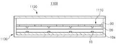
도 13을 참조하면, 본 발명의 예시적 실시예에 따른 조명 장치(1100)는 광원 모듈(1110) 및 상기 광원 모듈(1110) 상에 배치되는 커버(1120)를 포함할 수 있다. 그리고, 상기 광원 모듈(1110)을 수용하는 하우징(1130)을 더 포함할 수 있다.
Referring to FIG. 13, the
본 실시예에서 상기 광원 모듈(1110)은 상기 도 1에 도시된 실시예에 따른 광원 모듈(1)과 유사한 구성 및 구조를 가질 수 있다. 상기 광원 모듈(1110)의 각 구성 요소에 대한 구체적인 설명은 앞서 설명된 실시예(예를 들어, 도 1 참조)를 참조하여 이해될 수 있다.
In this embodiment, the
상기 커버(1120)는 필터 시트(30)가 부착된 도광판(20)과 분리되어 상기 도광판(20)의 상부 배치되며, 상기 도광판(20)을 덮을 수 있다. 조명 장치(1100)의 슬림화 구현을 위해서 상기 커버(1120)는 상기 광원 모듈(1110)의 기판(10a)과 대략 10mm의 간격을 가지도록 배치될 수 있다.
The
상기 커버(1120)는 일종의 디퓨저(diffuser)로서 상기 커버(1120)를 통과하는 광원(10)의 광이 충분히 분산되어 외부로 조사되도록 함으로써 전체적으로 균일한 휘도 분포를 갖는 면발광을 구현할 수 있도록 한다.
The
상기 커버(1120)는 광투과성을 갖는 수지 재질로 이루어질 수 있으며, 예를 들어, 폴리카보네이트(polycarbonate, PC), 폴리메틸메타크릴레이트(PMMA), 아크릴(acryl) 등을 포함할 수 있다.
The
상기 커버(1120)는 광분산 물질을 대략 3% 내지 15% 사이의 범위 내에서 함유할 수 있다. 상기 광분산 물질로는, 예를 들어, SiO2, TiO2 및 Al2O3로 구성된 그룹으로부터 선택된 하나 이상의 물질을 포함할 수 있다. 광분산 물질이 3%보다 적게 함유되는 경우에는 충분한 광분산 효과를 기대하기 어려울 수 있다. 그리고, 광분산 물질이 15% 이상 함유되는 경우에는 상기 커버(1120)를 통해 외부로 방출되는 광량이 감소하게 되어 광추출 효율이 저하될 수 있다.The
물론, 상기 광분산 물질은 선택적으로 함유될 수 있으며, 실시 형태에 따라서 생략될 수도 있다. 또한, 상기 커버(1120)의 표면에 미세한 요철 구조를 형성하는 것도 가능하다.
Of course, the light dispersing material may be selectively contained and may be omitted depending on the embodiment. It is also possible to form a fine concavo-convex structure on the surface of the
상기 하우징(1130)은 상기 광원 모듈(1110)을 수용하며, 외부 환경으로부터 상기 광원 모듈(1110)을 보호할 수 있다.The
상기 하우징(1130)은 상기 광원 모듈(1110)을 지지하는 프레임으로서의 기능과, 상기 광원 모듈(1110)에서 발생하는 열을 외부로 방출하는 히트 싱크로서의 기능을 수행할 수 있다. 이를 위해 상기 하우징(1130)은 열전도율이 높고 견고한 재질로 이루어질 수 있으며, 예를 들어, 알루미늄(Al)과 같은 금속 재질 또는 방열 수지 등으로 이루어질 수 있다.
The
본 실시예에 따른 조명 장치(1100)는 제품의 형태, 장소 및 목적 등에 따라서 광학 설계가 변경될 수 있다. 예를 들어, TV, 모니터 등의 디스플레이의 BLU(Backlight unit), 평판 조명이나 간접 조명 등 넓은 영역을 조사하는 조명 장치로 사용될 수 있다. 또한, 자동차의 테일 램프나 DRL(Daytime Running Light) 등에 적용될 수 있다. 특히, 커브드 디스플레이(curved display)와 같이 단순 평면이 아닌 곡선의 디자인을 가지는 경우에도 곡선에 맞게 용이하게 디자인이 가능하여 다양한 디자인의 광원으로 유연하게 적용할 수 있다.
In the
또한, 통신 기능을 부가하여 LED의 고유 목적과 통신 수단으로서의 목적을 동시에 달성하고자 하는 가시광 무선통신 기술도 가능하다. 이는 LED가 기존의 광원들에 비해 수명이 길고 전력 효율이 우수하며 다양한 색 구현이 가능할 뿐만 아니라 디지털 통신을 위한 스위칭 속도가 빠르고 디지털 제어가 가능하다는 장점을 갖고 있기 때문이다.In addition, a visible light wireless communication technology is also available in which a communication function is added to achieve the intrinsic purpose of an LED and the purpose of a communication means at the same time. This is because LEDs have a longer lifetime than conventional light sources, have excellent power efficiency, can realize various colors, and have a fast switching speed for digital communication and digital control.
가시광 무선통신 기술은 인간이 눈으로 인지할 수 있는 가시광 파장 대역의 빛을 이용하여 무선으로 정보를 전달하는 무선통신 기술이다. 이러한 가시광 무선통신 기술은 가시광 파장 대역의 빛을 이용한다는 측면에서 기존의 유선 광통신기술 및 적외선 무선통신과 구별되며, 통신 환경이 무선이라는 측면에서 유선 광통신 기술과 구별된다.The visible light wireless communication technology is a wireless communication technology that wirelessly transmits information using light of a visible light wavelength band that can be perceived by human eyes. Such a visible light wireless communication technology is distinguished from existing wired optical communication technology and infrared wireless communication in that it uses light in a visible light wavelength band and is distinguished from wired optical communication technology in terms of wireless communication environment.
또한, 가시광 무선통신 기술은 RF 무선통신과 달리 주파수 이용 측면에서 규제 또는 허가를 받지 않고 자유롭게 이용할 수 있다는 편리성과 물리적 보안성이 우수하고 통신 링크를 사용자가 눈으로 확인할 수 있다는 차별성을 가지고 있으며, 무엇보다도 광원의 고유 목적과 통신기능을 동시에 얻을 수 있다는 융합 기술로서의 특징을 가지고 있다.
In addition, unlike RF wireless communication, visible light wireless communication technology has the advantage that it can be freely used without being regulated or licensed in terms of frequency utilization, has excellent physical security, and has a difference in that a user can visually confirm a communication link. And has the characteristic of being a convergence technology that can obtain the intrinsic purpose of the light source and the communication function at the same time.
도 14는 예시적인 실시예들에 따른 광원 모듈을 채용한 바(bar) 타입의 램프의 분해 사시도이다.14 is an exploded perspective view of a bar-type lamp employing a light source module according to exemplary embodiments.
도 14를 참조하면, 조명 장치(1200)는 방열 부재(1210), 커버(1240), 광원 모듈(1250), 제1 소켓(1260) 및 제2 소켓(1270)을 포함할 수 있다.
14, the
방열 부재(1210)의 내부 또는/및 외부 표면에 다수개의 방열 핀(1211, 1212)이 요철 형태로 형성될 수 있으며, 방열 핀(1211, 1212)은 다양한 형상 및 간격을 갖도록 설계될 수 있다.A plurality of
방열 부재(1210)의 내측에는 돌출 형태의 지지대(1231)가 형성되어 있다. 지지대(1231)에는 광원 모듈(1250)이 고정될 수 있다. 방열 부재(1210)의 양 끝단에는 걸림 턱(1232)이 형성될 수 있다.A protruding
커버(1240)에는 걸림 홈(1242)이 형성되어 있으며, 걸림 홈(1242)에는 방열 부재(1210)의 걸림 턱(1232)이 후크 결합 구조로 결합될 수 있다. 걸림 홈(1242)과 걸림 턱(1232)이 형성되는 위치는 서로 바뀔 수도 있다.
The
상기 광원 모듈(1250)은 인쇄회로기판(1251), 복수의 광원(1252), 컨트롤러(1253), 필터 시트(1255)가 부착된 도광판(1254)를 포함할 수 있다. 상기 컨트롤러(1253)는 상기 복수의 광원(1252)의 구동 정보를 저장할 수 있다. 상기 인쇄회로기판(1251)에는 상기 복수의 광원(1252)을 동작시키기 위한 회로 배선들이 형성되어 있다. 또한, 상기 복수의 광원(1252)을 동작시키기 위한 구성 요소들이 포함될 수도 있다.The
상기 도광판(1254)은 상기 복수의 광원(1252) 상에 배치되며, 상면에는 복수의 홈부(미도시)가 구비될 수 있다. 상기 도광판(1254)의 상면은 복수의 패턴이 형성된 상기 필터 시트(1255)가 부착될 수 있다.The
본 실시예에서 상기 광원 모듈(1250)은 상기 도 1에 도시된 실시예에 따른 광원 모듈(1)과 유사한 구성 및 구조를 가질 수 있다. 상기 광원 모듈(1250)의 각 구성 요소에 대한 구체적인 설명은 앞서 설명된 실시예(예를 들어, 도 1 참조)를 참조하여 이해될 수 있다.
In this embodiment, the
제1 및 2 소켓(1260, 1270)은 한 쌍의 소켓으로서 방열 부재(1210) 및 커버(1240)로 구성된 원통형 커버 유닛의 양단에 결합되는 구조를 갖는다. 예를 들어, 제1 소켓(1260)은 전극 단자(1261) 및 전원 장치(1262)를 포함할 수 있고, 제2 소켓(1270)에는 더미 단자(1271)가 배치될 수 있다. 또한, 제1 소켓(1260) 또는 제2 소켓(1270) 중의 어느 하나의 소켓에 광센서 및/또는 통신 모듈이 내장될 수 있다. 예를 들어, 더미 단자(1271)가 배치된 제2 소켓(1270)에 광센서 및/또는 통신 모듈이 내장될 수 있다. 다른 예로서, 전극 단자(1261)가 배치된 제1 소켓(1260)에 광센서 및/또는 통신 모듈이 내장될 수도 있다.
The first and
본 발명에서 사물인터넷(Internet Of Things; IoT) 기기는 접근 가능한 유선 또는 무선 인터페이스를 가지며, 유선/무선 인터페이스를 통하여 적어도 하나 이상의 다른 기기와 통신하여, 데이터를 송신 또는 수신하는 기기들을 포함할 수 있다. 상기 접근 가능한 인터페이스는 유선 근거리통신망(Local Area Network; LAN), Wi-Fi(Wireless Fidelity)와 같은 무선 근거리 통신망 (Wireless Local Area Network; WLAN), 블루투스(Bluetooth)와 같은 무선 개인 통신망(Wireless Personal Area Network; WPAN), 무선 USB (Wireless Universal Serial Bus), Zigbee, NFC (Near Field Communication), RFID (Radio-frequency identification), PLC(Power Line communication), 또는 3G (3rd Generation), 4G (4th Generation), LTE (Long Term Evolution) 등 이동 통신망(mobile cellular network)에 접속 가능한 모뎀 통신 인터페이스 등을 포함할 수 있다. 상기 블루투스 인터페이스는 BLE(Bluetooth Low Energy)를 지원할 수 있다.
In the present invention, an Internet Of Things (IoT) device has an accessible wired or wireless interface and may include devices that communicate with at least one or more other devices via a wired / wireless interface to transmit or receive data . The accessible interface may be a wireless local area network (WLAN) such as a wired local area network (LAN), a wireless fidelity (Wi-Fi), a wireless personal area (WPAN), wireless USB (Universal Serial Bus), Zigbee, NFC (Near Field Communication), RFID (Radio Frequency Identification), PLC (Power Line Communication) , A modem communication interface that can be connected to a mobile cellular network such as LTE (Long Term Evolution), and the like. The Bluetooth interface may support BLE (Bluetooth Low Energy).
도 15는 예시적인 실시예들에 따른 광원 모듈을 채용할 수 있는 실내용 조명제어 네트워크 시스템이다.15 is an interior lighting control network system capable of employing a light source module according to exemplary embodiments.
본 실시예에 따른 네트워크 시스템(2000)은 LED 등의 반도체 발광소자를 이용하는 조명 기술과 사물인터넷(IoT) 기술, 무선 통신 기술 등이 융합된 복합적인 스마트 조명-네트워크 시스템일 수 있다. 네트워크 시스템(2000)은, 다양한 조명 장치 및 유무선 통신 장치를 이용하여 구현될 수 있으며, 센서, 컨트롤러, 통신수단, 네트워크 제어 및 유지 관리 등을 위한 소프트웨어 등에 의해 구현될 수 있다.The
네트워크 시스템(2000)은 가정이나 사무실 같이 건물 내에 정의되는 폐쇄적인 공간은 물론, 공원, 거리 등과 같이 개방된 공간 등에도 적용될 수 있다. 네트워크 시스템(2000)은, 다양한 정보를 수집/가공하여 사용자에게 제공할 수 있도록, 사물인터넷 환경에 기초하여 구현될 수 있다. 이때, 네트워크 시스템(2000)에 포함되는 LED 램프(2200)는, 주변 환경에 대한 정보를 게이트웨이(2100)로부터 수신하여 LED 램프(2200) 자체의 조명을 제어하는 것은 물론, LED 램프(2200)의 가시광 통신 등의 기능에 기초하여 사물인터넷 환경에 포함되는 다른 장치들(2300~2800)의 동작 상태 확인 및 제어 등과 같은 역할을 수행할 수도 있다.
The
도 15를 참조하면, 네트워크 시스템(2000)은, 서로 다른 통신 프로토콜에 따라 송수신되는 데이터를 처리하기 위한 게이트웨이(2100), 게이트웨이(2100)와 통신 가능하도록 연결되며 LED를 광원으로 포함하는 LED 램프(2200), 및 다양한 무선 통신 방식에 따라 게이트웨이(2100)와 통신 가능하도록 연결되는 복수의 장치(2300~2800)를 포함할 수 있다. 사물인터넷 환경에 기초하여 네트워크 시스템(2000)을 구현하기 위해, LED 램프(2200)를 비롯한 각 장치(2300~2800)들은 적어도 하나의 통신 모듈을 포함할 수 있다. 일 실시예로, LED 램프(2200)는 WiFi, 지그비(Zigbee), LiFi 등의 무선 통신 프로토콜에 의해 게이트웨이(2100)와 통신 가능하도록 연결될 수 있으며, 이를 위해 적어도 하나의 램프용 통신 모듈(2210)을 가질 수 있다.15, the
앞서 설명한 바와 같이, 네트워크 시스템(2000)은 가정이나 사무실 같이 폐쇄적인 공간은 물론 거리나 공원 같은 개방적인 공간에도 적용될 수 있다. 네트워크 시스템(2000)이 가정에 적용되는 경우, 네트워크 시스템(2000)에 포함되며 사물인터넷 기술에 기초하여 게이트웨이(2100)와 통신 가능하도록 연결되는 복수의 장치(2300~2800)는 냉장고(2320), 텔레비전(2310) 등의 가전 제품(2300), 디지털 도어록(2400), 차고 도어록(2500), 벽 등에 설치되는 조명용 스위치(2600), 무선 통신망 중계를 위한 라우터(2700) 및 스마트 폰, 태블릿, 랩톱 컴퓨터 등의 모바일 기기(2800) 등을 포함할 수 있다.
As described above, the
네트워크 시스템(2000)에서, LED 램프(2200)는 가정 내에 설치된 무선 통신 네트워크(Zigbee, WiFi, LiFi 등)를 이용하여 다양한 장치(2300~2800)의 동작 상태를 확인하거나, 주위 환경/상황에 따라 LED 램프(2200) 자체의 조도를 자동으로 조절할 수 있다. 또한 LED 램프(2200)는 LED 램프(2200)에서 방출되는 가시광선을 이용한 LiFi(LED WiFi) 통신을 이용하여 네트워크 시스템(2000)에 포함되는 장치들(2300~2800)을 컨트롤할 수도 있다.In the
우선, LED 램프(2200)는 램프용 통신 모듈(2210)을 통해 게이트웨이(2100)로부터 전달되는 주변 환경, 또는 LED 램프(2200)에 장착된 센서로부터 수집되는 주변 환경 정보에 기초하여 LED 램프(2200)의 조도를 자동으로 조절할 수 있다. 예를 들면, 텔레비전(2310)에서 방송되고 있는 프로그램의 종류 또는 화면의 밝기에 따라 LED 램프(2200)의 조명 밝기는 자동으로 조절될 수 있다. 이를 위해, LED 램프(2200)는 게이트웨이(2100)와 연결된 램프용 통신 모듈(2210)로부터 텔레비전(2310)의 동작 정보를 수신할 수 있다. 램프용 통신 모듈(2210)은 LED 램프(2200)에 포함되는 센서 및/또는 컨트롤러와 일체형으로 모듈화될 수 있다.The
예를 들어, TV프로그램에서 방영되는 프로그램 값이 휴먼드라마일 경우, 미리 설정된 설정 값에 따라 조명도 거기에 맞게 12,000 K 이하의 색 온도로(예를 들면 6,000 K로) 낮아지고 색감이 조절되어 아늑한 분위기를 연출할 수 있다. 반대로 프로그램 값이 개그프로그램인 경우, 조명도 설정값에 따라 색 온도가 6,000 K 이상으로 높아지고 푸른색 계열의 백색조명으로 조절되도록 네트워크 시스템(2000)이 구성될 수 있다.For example, when the program value of a TV program is a human drama, the lighting is lowered to a color temperature of 12,000 K or less (for example, 6,000 K) according to a predetermined setting value, Atmosphere can be produced. Conversely, when the program value is a gag program, the
또한, 가정 내에 사람이 없는 상태에서 디지털 도어록(2400)이 잠긴 후 일정 시간이 경과하면, 턴-온된 LED 램프(2200)를 모두 턴-오프시켜 전력 낭비를 방지할 수 있다. 또는, 모바일 기기(2800) 등을 통해 보안 모드가 설정된 경우, 가정 내에 사람이 없는 상태에서 디지털 도어록(2400)이 잠기면, LED 램프(2200)를 턴-온 상태로 유지시킬 수도 있다.
Also, when the
LED 램프(2200)의 동작은, 네트워크 시스템(2000)과 연결되는 다양한 센서를 통해 수집되는 주변 환경에 따라서 제어될 수도 있다. 예를 들어 네트워크 시스템(2000)이 건물 내에 구현되는 경우, 빌딩 내에서 조명과 위치센서와 통신모듈을 결합하고, 건물 내 사람들의 위치정보를 수집하여 조명을 턴-온 또는 턴-오프하거나 수집한 정보를 실시간으로 제공하여 시설관리나 유휴공간의 효율적 활용을 가능케 할 수 있다. 일반적으로 LED 램프(2200)와 같은 조명 장치는, 건물 내 각 층의 거의 모든 공간에 배치되므로, LED 램프(2200)와 일체로 제공되는 센서를 통해 건물 내의 각종 정보를 수집하고 이를 시설관리, 유휴공간의 활용 등에 이용할 수 있다.The operation of the
한편, LED 램프(2200)는 이미지센서, 저장장치, 램프용 통신 모듈(2210) 등과 결합하여, 건물 보안을 유지하거나 긴급상황을 감지하고 대응할 수 있는 장치로 활용할 수 있다. 예를 들어 LED 램프(2200)에 연기 또는 온도 감지 센서 등이 부착된 경우, 화재 발생 여부 등을 신속하게 감지함으로써 피해를 최소화할 수 있다. 또한 외부의 날씨나 일조량 등을 고려하여 조명의 밝기를 조절, 에너지를 절약하고 쾌적한 조명환경을 제공할 수도 있다.
The
도 16은 예시적인 실시예들에 따른 광원 모듈을 채용할 수 있는 개방형 네트워크 시스템이다.16 is an open network system capable of employing a light source module according to exemplary embodiments.
도 16을 참조하면, 본 실시예에 따른 네트워크 시스템(2000')은 통신 연결 장치(2100'), 소정의 간격마다 설치되어 통신 연결 장치(2100')와 통신 가능하도록 연결되는 복수의 조명 기구(2200', 2300'), 서버(2400'), 서버(2400')를 관리하기 위한 컴퓨터(2500'), 통신 기지국(2600'), 통신 가능한 상기 장비들을 연결하는 통신망(2700'), 및 모바일 기기(2800') 등을 포함할 수 있다.Referring to FIG. 16, the network system 2000 'according to the present embodiment includes a communication connection device 2100', a plurality of lighting devices installed at predetermined intervals and connected to communicate with the communication connection device 2100 ' 2200 ', 2300', a server 2400 ', a computer 2500' for managing the server 2400 ', a communication base station 2600', a communication network 2700 ' Device 2800 ', and the like.
거리 또는 공원 등의 개방적인 외부 공간에 설치되는 복수의 조명 기구(2200', 2300') 각각은 스마트 엔진(2210', 2310')을 포함할 수 있다. 스마트 엔진(2210', 2310')은 빛을 내기 위한 반도체 발광소자, 반도체 발광소자를 구동하기 위한 구동 드라이버 외에 주변 환경의 정보를 수집하는 센서, 및 통신 모듈 등을 포함할 수 있다. 상기 통신 모듈에 의해 스마트 엔진(2210', 2310')은 WiFi, Zigbee, LiFi 등의 통신 프로토콜에 따라 주변의 다른 장비들과 통신할 수 있다.Each of a plurality of lighting devices 2200 ', 2300' installed in an open external space such as a street or a park may include a smart engine 2210 ', 2310'. The smart engines 2210 'and 2310' may include a semiconductor light emitting device for emitting light, a driving driver for driving the semiconductor light emitting device, a sensor for collecting information on the surrounding environment, and a communication module. The communication module enables the smart engines 2210 'and 2310' to communicate with other nearby devices according to communication protocols such as WiFi, Zigbee, LiFi, and the like.
일례로, 하나의 스마트 엔진(2210')은 다른 스마트 엔진(2310')과 통신 가능하도록 연결될 수 있다. 이때, 스마트 엔진(2210', 2310') 상호 간의 통신에는 WiFi 확장 기술(WiFi Mesh)이 적용될 수 있다. 적어도 하나의 스마트 엔진(2210')은 통신망(2700')에 연결되는 통신 연결 장치(2100')와 유/무선 통신에 의해 연결될 수 있다. 통신의 효율을 높이기 위해, 몇 개의 스마트 엔진(2210', 2310')을 하나의 그룹으로 묶어 하나의 통신 연결 장치(2100')와 연결할 수 있다.
In one example, one smart engine 2210 'may be communicatively coupled to another smart engine 2310'. At this time, the WiFi extension technology (WiFi mesh) may be applied to the communication between the smart engines 2210 'and 2310'. At least one smart engine 2210 'may be connected to the communication link 2100' connected to the communication network 2700 'by wire / wireless communication. In order to increase the efficiency of communication, several smart engines 2210 'and 2310' may be grouped into one group and connected to one communication connection device 2100 '.
통신 연결 장치(2100')는 유/무선 통신이 가능한 액세스 포인트(access point, AP)로서, 통신망(2700')과 다른 장비 사이의 통신을 중개할 수 있다. 통신 연결 장치(2100')는 유/무선 방식 중 적어도 하나에 의해 통신망(2700')과 연결될 수 있으며, 일례로 조명 기구(2200', 2300') 중 어느 하나의 내부에 기구적으로 수납될 수 있다.The communication connection device 2100 'is an access point (AP) capable of wired / wireless communication, and can mediate communication between the communication network 2700' and other devices. The communication connection device 2100 'may be connected to the communication network 2700' by at least one of wire / wireless methods and may be mechanically housed in any one of the lighting devices 2200 ', 2300' have.
통신 연결 장치(2100')는 WiFi 등의 통신 프로토콜을 통해 모바일 기기(2800')와 연결될 수 있다. 모바일 기기(2800')의 사용자는 인접한 주변의 조명 기구(2200')의 스마트 엔진(2210')과 연결된 통신 연결 장치(2100')를 통해, 복수의 스마트 엔진(2210', 2310')이 수집한 주변 환경 정보를 수신할 수 있다. 상기 주변 환경 정보는 주변 교통 정보, 날씨 정보 등을 포함할 수 있다. 모바일 기기(2800')는 통신 기지국(2600')을 통해 3G 또는 4G 등의 무선 셀룰러 통신 방식으로 통신망(2700')에 연결될 수도 있다.The communication connection device 2100 'may be connected to the mobile device 2800' via a communication protocol such as WiFi. A user of the mobile device 2800'may collect a plurality of smart engines 2210'and 2310'through the communication connection 2100'connected to the smart engine 2210'of the adjacent surrounding lighting device 2200' It is possible to receive the surrounding information. The surrounding environment information may include surrounding traffic information, weather information, and the like. The mobile device 2800 'may be connected to the communication network 2700' in a wireless cellular communication manner such as 3G or 4G via the communication base station 2600 '.
한편, 통신망(2700')에 연결되는 서버(2400')는, 각 조명 기구(2200', 2300')에 장착된 스마트 엔진(2210', 2310')이 수집하는 정보를 수신함과 동시에, 각 조명 기구(2200', 2300')의 동작 상태 등을 모니터링 할 수 있다. 각 조명 기구(2200', 2300')의 동작 상태의 모니터링 결과에 기초하여 각 조명 기구(2200', 2300')를 관리하기 위해, 서버(2400')는 관리 시스템을 제공하는 컴퓨터(2500')와 연결될 수 있다. 컴퓨터(2500')는 각 조명 기구(2200', 2300'), 특히 스마트 엔진(2210', 2310')의 동작 상태를 모니터링하고 관리할 수 있는 소프트웨어 등을 실행할 수 있다.
On the other hand, the server 2400 'connected to the communication network 2700' receives the information collected by the smart engines 2210 'and 2310' mounted on the respective lighting apparatuses 2200 'and 2300' The operation state of the mechanisms 2200 'and 2300', and the like. To manage each luminaire 2200 ', 2300' based on the monitoring results of the operational status of each luminaire 2200 ', 2300', the server 2400 'includes a computer 2500'Lt; / RTI > The computer 2500 'may execute software or the like that can monitor and manage the operational status of each lighting apparatus 2200', 2300 ', particularly the smart engines 2210', 2310 '.
도 17은 예시적인 실시예들에 따른 광원 모듈을 채용할 수 있는 가시광 무선 통신에 의한 조명 기구의 스마트 엔진과 모바일 기기의 통신 동작을 설명하기 위한 블록도이다.17 is a block diagram for explaining a communication operation between a smart engine and a mobile device of a lighting device by visible light wireless communication capable of employing a light source module according to exemplary embodiments.
도 17을 참조하면, 스마트 엔진(2210')은 신호 처리부(2211'), 제어부(2212'), LED 드라이버(2213'), 광원부(2214'), 센서(2215') 등을 포함할 수 있다. 스마트 엔진(2210')과 가시광 무선통신에 의해 연결되는 모바일 기기(2800')는, 제어부(2801'), 수광부(2802'), 신호처리부(2803'), 메모리(2804'), 입출력부(2805') 등을 포함할 수 있다.
17, the smart engine 2210 'may include a signal processing unit 2211', a control unit 2212 ', an LED driver 2213', a light source unit 2214 ', a sensor 2215' . The mobile device 2800 'connected to the smart engine 2210' by visible light wireless communication includes a control unit 2801 ', a light receiving unit 2802', a signal processing unit 2803 ', a memory 2804', an input / output unit 2805 ') and the like.
가시광 무선통신(LiFi) 기술은 인간이 눈으로 인지할 수 있는 가시광 파장 대역의 빛을 이용하여 무선으로 정보를 전달하는 무선통신 기술이다. 이러한 가시광 무선통신 기술은 가시광 파장 대역의 빛, 즉 상기 실시예에서 설명한 발광 패키지로부터의 특정 가시광 주파수를 이용한다는 측면에서 기존의 유선 광통신기술 및 적외선 무선통신과 구별되며, 통신 환경이 무선이라는 측면에서 유선 광통신 기술과 구별된다. 또한, 가시광 무선통신 기술은 RF 무선통신과 달리 주파수 이용 측면에서 규제 또는 허가를 받지 않고 자유롭게 이용할 수 있어 편리하고 물리적 보안성이 우수하고 통신 링크를 사용자가 눈으로 확인할 수 있다는 차별성을 가지고 있으며, 무엇보다도 광원의 고유 목적과 통신기능을 동시에 얻을 수 있다는 융합 기술로서의 특징을 가지고 있다.The visible light wireless communication (LiFi) technology is a wireless communication technology that wirelessly transmits information by using visible light wavelength band visible to the human eye. Such visible light wireless communication technology is distinguished from existing wired optical communication technology and infrared wireless communication in that it utilizes light of a visible light wavelength band, that is, a specific visible light frequency from the light emitting package described in the above embodiment, It is distinguished from wired optical communication technology. In addition, unlike RF wireless communication, visible light wireless communication technology can be freely used without being regulated or licensed in terms of frequency utilization, so that it has excellent physical security and a communication link can be visually recognized by the user. And has the characteristic of being a convergence technology that can obtain the intrinsic purpose of the light source and the communication function at the same time.
스마트 엔진(2210')의 신호 처리부(2211')는, 가시광 무선통신에 의해 송수신하고자 하는 데이터를 처리할 수 있다. 일 실시예로, 신호 처리부(2211')는 센서(2215')에 의해 수집된 정보를 데이터로 가공하여 제어부(2212')에 전송할 수 있다. 제어부(2212')는 신호 처리부(2211')와 LED 드라이버(2213') 등의 동작을 제어할 수 있으며, 특히 신호 처리부(2211')가 전송하는 데이터에 기초하여 LED 드라이버(2213')의 동작을 제어할 수 있다. LED 드라이버(2213')는 제어부(2212')가 전달하는 제어 신호에 따라 광원부(2214')를 발광시킴으로써, 데이터를 모바일 기기(2800')로 전달할 수 있다.The signal processing unit 2211 'of the smart engine 2210' can process data to be transmitted / received by visible light wireless communication. In one embodiment, the signal processing unit 2211 'may process the information collected by the sensor 2215' into data and transmit it to the control unit 2212 '. The control unit 2212 'can control the operation of the signal processing unit 2211' and the LED driver 2213 ', and in particular, the operation of the LED driver 2213' based on the data transmitted by the signal processing unit 2211 ' Can be controlled. The LED driver 2213 'may transmit the data to the mobile device 2800' by emitting the light source portion 2214 'according to a control signal transmitted from the control portion 2212'.
모바일 기기(2800')는 제어부(2801'), 데이터를 저장하는 메모리(2804'), 디스플레이와 터치스크린, 오디오 출력부 등을 포함하는 입출력부(2805'), 신호 처리부(2803') 외에 데이터가 포함된 가시광을 인식하기 위한 수광부(2802')를 포함할 수 있다. 수광부(2802')는 가시광을 감지하여 이를 전기 신호로 변환할 수 있으며, 신호 처리부(2803')는 수광부에 의해 변환된 전기 신호에 포함된 데이터를 디코딩할 수 있다. 제어부(2801')는 신호 처리부(2803')가 디코딩한 데이터를 메모리(2804')에 저장하거나 입출력부(2805') 등을 통해 사용자가 인식할 수 있도록 출력할 수 있다.
The
지금까지의 설명은 본 발명의 기술적 사상을 예시적으로 설명한 것에 불과한 것으로서, 본 발명이 속하는 기술분야에서 통상의 지식을 가진 자라면 본 발명의 본질적인 특성에서 벗어나지 않는 범위에서 다양한 수정 및 변형이 가능할 것이다.It will be apparent to those skilled in the art that various modifications and variations can be made in the present invention without departing from the spirit or essential characteristics thereof. .
따라서, 본 발명에 개시된 실시예들은 본 발명의 기술적 사상을 한정하기 위한 것이 아니라 설명하기 위한 것이고, 이러한 실시예에 의하여 본 발명의 기술 사상의 범위가 한정되는 것은 아니다. 본 발명의 보호 범위는 아래의 청구범위에 의하여 해석되어야 하며, 그와 동등한 범위 내에 있는 모든 기술적 사상은 본 발명의 권리범위에 포함되는 것으로 해석되어야 할 것이다.
Therefore, the embodiments disclosed in the present invention are not intended to limit the technical spirit of the present invention, but are intended to illustrate and not limit the scope of the technical spirit of the present invention. The scope of protection of the present invention should be construed according to the following claims, and all technical ideas which are within the scope of the same should be interpreted as being included in the scope of the present invention.
1, 2, 3... 광원 모듈
10... 광원
20, 40, 50... 도광판
20a, 40a, 50a... 홈부
30... 필터 시트
31... 패턴1, 2, 3 ... light source module
10 ... light source
20, 40, 50 ... light guide plate
20a, 40a, 50a, ...,
30 ... filter sheet
31 ... pattern
Claims (20)
Translated fromKorean상기 광원 상에 배치되며, 상면에 홈부를 구비하는 도광판; 및
상기 도광판의 상면에 부착되며, 상기 광원의 광을 부분적으로 투과시키고 부분적으로 반사시키는 패턴을 가지는 필터 시트;
를 포함하는 광원 모듈.
Light source;
A light guide plate disposed on the light source and having a groove on an upper surface thereof; And
A filter sheet attached to an upper surface of the light guide plate and having a pattern partially transmitting and partially reflecting light of the light source;
.
상기 패턴은, 상기 홈부 상에 배치되어 상기 홈부를 덮으며, 반사 물질을 포함하고 방사상으로 배열된 복수의 도트를 가지는 것을 특징으로 하는 광원 모듈.
The method according to claim 1,
Wherein the pattern has a plurality of dots disposed on the groove portion to cover the groove portion and including a reflective material and arranged in a radial direction.
상기 복수의 도트는 배열되는 영역에 따라서 서로 다른 크기를 가지는 것을 특징으로 하는 광원 모듈.
3. The method of claim 2,
Wherein the plurality of dots have different sizes depending on regions to be arranged.
상기 복수의 도트는 상기 홈부에서 멀어질수록 작은 크기를 가지는 것을 특징으로 하는 광원 모듈.
3. The method of claim 2,
Wherein the plurality of dots have a smaller size as the distance from the groove is increased.
상기 복수의 도트는 상기 홈부에서 멀어질수록 상기 복수의 도트 사이의 간격이 커지는 것을 특징으로 하는 광원 모듈.
3. The method of claim 2,
Wherein a distance between the plurality of dots increases as the distance from the groove increases.
상기 패턴은, 상기 홈부 상에 배치되어 상기 홈부를 덮으며 상기 도광판의 상면 중 적어도 일부를 노출시키고, 방사상으로 배열되는 복수의 홀을 가지는 것을 특징으로 하는 광원 모듈.
The method according to claim 1,
Wherein the pattern has a plurality of holes arranged on the groove portion, covering the groove portion, exposing at least a part of the upper surface of the light guide plate, and radially arranged.
상기 복수의 홀은 상기 홈부에서 멀어질수록 큰 크기를 가지는 것을 특징으로 하는 광원 모듈.
The method according to claim 6,
Wherein the plurality of holes have a larger size as the distance from the groove is increased.
상기 복수의 홀은 상기 홈부에서 멀어질수록 상기 복수의 홀 사이의 간격이 작아지는 것을 특징으로 하는 광원 모듈.
The method according to claim 6,
Wherein a distance between the plurality of holes decreases as the distance from the groove increases.
상기 홈부는 상기 광원과 마주하여 위치하는 것을 특징으로 하는 광원 모듈.
The method according to claim 1,
And the groove portion is located facing the light source.
상기 홈부는 상기 광원을 향해 함몰된 꼭짓점이 상기 광원의 광축에 놓이는 것을 특징으로 하는 광원 모듈.
10. The method of claim 9,
Wherein the groove portion is located at an optical axis of the light source, the vertex being recessed toward the light source.
상기 홈부를 채우는 광확산부를 더 포함하는 것을 특징으로 하는 광원 모듈.
The method according to claim 1,
And a light diffusing unit for filling the groove.
상기 광확산부는 광확산물질로 SiO2, TiO2 및 Al2O3로 구성된 그룹으로부터 선택된 하나 이상의 물질을 함유하는 것을 특징으로 하는 광원 모듈.
12. The method of claim 11,
Wherein the light diffusing part contains at least one material selected from the group consisting of SiO2 , TiO2 and Al2 O3 as a light diffusing material.
상기 도광판은 하면에 함몰 형성되어 상기 광원을 수용하는 수용홈을 더 포함하는 것을 특징으로 하는 광원 모듈.
The method according to claim 1,
Wherein the light guide plate further comprises a receiving groove formed in a lower surface thereof to receive the light source.
상기 광원은 반도체 발광다이오드(LED) 칩 또는 LED 칩이 장착된 LED 패키지인 것을 특징으로 하는 광원 모듈.
The method according to claim 1,
Wherein the light source is an LED package equipped with a semiconductor light emitting diode (LED) chip or an LED chip.
상기 복수의 광원과 마주하는 제1면, 상기 제1면의 반대에 배치되는 제2면, 상기 제1면과 제2면 사이의 제3면을 포함하는 도광판; 및
상기 도광판의 상면에 부착되는 필터 시트;
를 포함하고,
상기 도광판은 상기 제2면에 상기 복수의 광원과 대응되는 위치에 함몰된 복수의 홈부를 가지며,
상기 필터 시트는 상기 복수의 홈부를 덮는 복수의 패턴을 가지며, 상기 광원의 광을 부분적으로 투과시키고 부분적으로 반사시키는 것을 특징으로 하는 광원 모듈.
A plurality of light sources;
A light guide plate including a first surface facing the plurality of light sources, a second surface disposed opposite to the first surface, and a third surface between the first surface and the second surface; And
A filter sheet attached to an upper surface of the light guide plate;
Lt; / RTI >
Wherein the light guide plate has a plurality of grooves recessed at positions corresponding to the plurality of light sources on the second surface,
Wherein the filter sheet has a plurality of patterns covering the plurality of grooves, and partially transmits and partially reflects light of the light source.
상기 각 패턴은 반사 물질을 포함하는 복수의 도트가 방사상으로 배열된 구조를 가지는 것을 특징으로 하는 광원 모듈.
16. The method of claim 15,
Wherein each of the patterns has a structure in which a plurality of dots including a reflective material are radially arranged.
상기 각 패턴은 상기 도광판의 제2면 중 적어도 일부를 노출시키는 복수의 홀이 방사상으로 배열된 구조를 가지는 것을 특징으로 하는 광원 모듈.
16. The method of claim 15,
Wherein each of the patterns has a structure in which a plurality of holes exposing at least a part of the second surface of the light guide plate are radially arranged.
상기 복수의 광원이 장착되는 기판을 더 포함하는 광원 모듈.
16. The method of claim 15,
And a substrate on which the plurality of light sources are mounted.
상기 광원 모듈 상에 배치되는 커버;
를 포함하고,
상기 광원 모듈은,
광원;
상기 광원 상에 배치되며, 상면에 홈부를 구비하는 도광판; 및
상기 도광판의 상면에 부착되며, 상기 광원의 광을 부분적으로 투과시키고 부분적으로 반사시키는 패턴을 가지는 필터 시트;를 포함하는 조명 장치.
A light source module; And
A cover disposed on the light source module;
Lt; / RTI >
The light source module includes:
Light source;
A light guide plate disposed on the light source and having a groove on an upper surface thereof; And
And a filter sheet attached to an upper surface of the light guide plate and having a pattern partially transmitting and partially reflecting light of the light source.
상기 광원 모듈을 수용하는 하우징을 더 포함하는 것을 특징으로 하는 조명 장치.
20. The method of claim 19,
Further comprising a housing for receiving the light source module.
Priority Applications (3)
| Application Number | Priority Date | Filing Date | Title |
|---|---|---|---|
| KR1020160029453AKR20170106575A (en) | 2016-03-11 | 2016-03-11 | Light source module and lighting apparatus having the same |
| US15/280,253US9897266B2 (en) | 2016-03-11 | 2016-09-29 | Light source module and lighting apparatus including the same |
| CN201710145296.XACN107178712A (en) | 2016-03-11 | 2017-03-13 | Light source module and the lighting device including it |
Applications Claiming Priority (1)
| Application Number | Priority Date | Filing Date | Title |
|---|---|---|---|
| KR1020160029453AKR20170106575A (en) | 2016-03-11 | 2016-03-11 | Light source module and lighting apparatus having the same |
Publications (1)
| Publication Number | Publication Date |
|---|---|
| KR20170106575Atrue KR20170106575A (en) | 2017-09-21 |
Family
ID=59787881
Family Applications (1)
| Application Number | Title | Priority Date | Filing Date |
|---|---|---|---|
| KR1020160029453AWithdrawnKR20170106575A (en) | 2016-03-11 | 2016-03-11 | Light source module and lighting apparatus having the same |
Country Status (3)
| Country | Link |
|---|---|
| US (1) | US9897266B2 (en) |
| KR (1) | KR20170106575A (en) |
| CN (1) | CN107178712A (en) |
Cited By (6)
| Publication number | Priority date | Publication date | Assignee | Title |
|---|---|---|---|---|
| KR20180119538A (en)* | 2018-10-15 | 2018-11-02 | 주식회사 소룩스 | lighting apparatus based on fluorescent printed reflector and lighting apparatus based on printing fluorescent |
| KR20190100132A (en)* | 2018-02-13 | 2019-08-28 | 국민대학교산학협력단 | Colorful Thin Film Solar Cell for Minimizing Efficiency Reduction |
| US10862004B2 (en) | 2017-12-13 | 2020-12-08 | Samsung Electronics Co., Ltd. | Ultraviolet semiconductor light emitting devices |
| WO2022019474A1 (en)* | 2020-07-20 | 2022-01-27 | 삼성전자주식회사 | Backlight unit and display apparatus comprising same |
| US20230013230A1 (en)* | 2021-07-13 | 2023-01-19 | Lg Electronics Inc. | Refrigerator and home appliance |
| US20230018403A1 (en)* | 2021-07-13 | 2023-01-19 | Lg Electronics Inc. | Panel assembly for a home appliance and home appliance therewith |
Families Citing this family (20)
| Publication number | Priority date | Publication date | Assignee | Title |
|---|---|---|---|---|
| JP6150020B2 (en)* | 2015-02-20 | 2017-06-21 | 三菱電機株式会社 | Light guide, light source device and image reading device |
| US9633883B2 (en) | 2015-03-20 | 2017-04-25 | Rohinni, LLC | Apparatus for transfer of semiconductor devices |
| KR102432261B1 (en)* | 2016-09-29 | 2022-08-16 | 루미리즈 홀딩 비.브이. | Lighting assembly with diffuser |
| US10141215B2 (en) | 2016-11-03 | 2018-11-27 | Rohinni, LLC | Compliant needle for direct transfer of semiconductor devices |
| US10504767B2 (en) | 2016-11-23 | 2019-12-10 | Rohinni, LLC | Direct transfer apparatus for a pattern array of semiconductor device die |
| CN109212826B (en)* | 2017-06-29 | 2021-07-27 | 中强光电股份有限公司 | Light source module |
| JP7032645B2 (en)* | 2018-03-26 | 2022-03-09 | 日亜化学工業株式会社 | Light emitting module and its manufacturing method |
| KR102594815B1 (en)* | 2018-06-20 | 2023-10-30 | 엘지이노텍 주식회사 | Lighting module and lighting apparatus |
| DE102018117591A1 (en) | 2018-07-20 | 2020-01-23 | Osram Opto Semiconductors Gmbh | Optoelectronic component and display device |
| US11094571B2 (en) | 2018-09-28 | 2021-08-17 | Rohinni, LLC | Apparatus to increase transferspeed of semiconductor devices with micro-adjustment |
| TWI680573B (en)* | 2018-11-02 | 2019-12-21 | 友達光電股份有限公司 | Display panel and pixel structure thereof |
| CN109613642B (en)* | 2018-11-30 | 2020-07-07 | 合肥泰沃达智能装备有限公司 | Semi-reflecting and semi-permeable light guide plate |
| JP6680349B1 (en)* | 2018-12-28 | 2020-04-15 | 日亜化学工業株式会社 | Light emitting module |
| US11073654B2 (en)* | 2018-12-28 | 2021-07-27 | Nichia Corporation | Light emitting module with recesses in light guide plate |
| DE102020115536A1 (en) | 2019-06-21 | 2020-12-24 | Lg Display Co., Ltd. | Light guide film, backlight unit and display device |
| JP7041364B2 (en)* | 2019-08-02 | 2022-03-24 | 日亜化学工業株式会社 | Light emitting device |
| JP7213454B2 (en)* | 2019-09-30 | 2023-01-27 | 日亜化学工業株式会社 | light emitting module |
| USD899384S1 (en) | 2019-11-04 | 2020-10-20 | Putco, Inc. | Surface-mount device |
| TW202202777A (en) | 2020-06-04 | 2022-01-16 | 日商日亞化學工業股份有限公司 | Planar light source and method of manufacturing planar light source |
| JP2024145784A (en)* | 2023-03-31 | 2024-10-15 | 日亜化学工業株式会社 | Planar light source, liquid crystal display device |
Family Cites Families (44)
| Publication number | Priority date | Publication date | Assignee | Title |
|---|---|---|---|---|
| CN1143394C (en) | 1996-08-27 | 2004-03-24 | 精工爱普生株式会社 | Peeling method, thin film device transfer method and thin film device |
| USRE38466E1 (en) | 1996-11-12 | 2004-03-16 | Seiko Epson Corporation | Manufacturing method of active matrix substrate, active matrix substrate and liquid crystal display device |
| US7208725B2 (en) | 1998-11-25 | 2007-04-24 | Rohm And Haas Electronic Materials Llc | Optoelectronic component with encapsulant |
| JP3906654B2 (en) | 2000-07-18 | 2007-04-18 | ソニー株式会社 | Semiconductor light emitting device and semiconductor light emitting device |
| US6818465B2 (en) | 2001-08-22 | 2004-11-16 | Sony Corporation | Nitride semiconductor element and production method for nitride semiconductor element |
| JP2003218034A (en) | 2002-01-17 | 2003-07-31 | Sony Corp | Selective growth method, semiconductor light emitting device and method of manufacturing the same |
| JP3815335B2 (en) | 2002-01-18 | 2006-08-30 | ソニー株式会社 | Semiconductor light emitting device and manufacturing method thereof |
| KR100499129B1 (en) | 2002-09-02 | 2005-07-04 | 삼성전기주식회사 | Light emitting laser diode and fabricatin method thereof |
| US7002182B2 (en) | 2002-09-06 | 2006-02-21 | Sony Corporation | Semiconductor light emitting device integral type semiconductor light emitting unit image display unit and illuminating unit |
| KR100714639B1 (en) | 2003-10-21 | 2007-05-07 | 삼성전기주식회사 | Light emitting element |
| KR100506740B1 (en) | 2003-12-23 | 2005-08-08 | 삼성전기주식회사 | Nitride semiconductor light emitting device and method of manufacturing the same |
| KR100664985B1 (en) | 2004-10-26 | 2007-01-09 | 삼성전기주식회사 | Nitride-based semiconductor device |
| KR100665222B1 (en) | 2005-07-26 | 2007-01-09 | 삼성전기주식회사 | LED package using diffusion material and manufacturing method thereof |
| KR100661614B1 (en) | 2005-10-07 | 2006-12-26 | 삼성전기주식회사 | Nitride-based semiconductor light emitting device and its manufacturing method |
| KR100723247B1 (en) | 2006-01-10 | 2007-05-29 | 삼성전기주식회사 | Chip coated LED package and manufacturing method thereof |
| KR101222152B1 (en) | 2006-02-06 | 2013-01-14 | 삼성디스플레이 주식회사 | Backlight assembly and display device having the same |
| KR100735325B1 (en) | 2006-04-17 | 2007-07-04 | 삼성전기주식회사 | Light emitting diode package and its manufacturing method |
| KR100930171B1 (en) | 2006-12-05 | 2009-12-07 | 삼성전기주식회사 | White light emitting device and white light source module using same |
| TW200825529A (en) | 2006-12-06 | 2008-06-16 | Chi Lin Technology Co Ltd | Light mixer and backlight module having it |
| KR100855065B1 (en) | 2007-04-24 | 2008-08-29 | 삼성전기주식회사 | Light emitting diode package |
| KR100982980B1 (en) | 2007-05-15 | 2010-09-17 | 삼성엘이디 주식회사 | Surface light source device and LCD backlight unit having same |
| KR101164026B1 (en) | 2007-07-12 | 2012-07-18 | 삼성전자주식회사 | Nitride semiconductor light emitting device and fabrication method thereof |
| KR100891761B1 (en) | 2007-10-19 | 2009-04-07 | 삼성전기주식회사 | Semiconductor light emitting device, manufacturing method thereof and semiconductor light emitting device package using same |
| CN101256307A (en)* | 2008-03-14 | 2008-09-03 | 上海广电光电子有限公司 | Directly-down backlight module unit |
| KR101332794B1 (en) | 2008-08-05 | 2013-11-25 | 삼성전자주식회사 | Light emitting device, light emitting system comprising the same, and fabricating method of the light emitting device and the light emitting system |
| KR20100030470A (en) | 2008-09-10 | 2010-03-18 | 삼성전자주식회사 | Light emitting device and system providing white light with various color temperatures |
| KR101530876B1 (en) | 2008-09-16 | 2015-06-23 | 삼성전자 주식회사 | Light emitting device with increased light emitting amount, light emitting device including same, method of manufacturing light emitting device and light emitting device |
| US8008683B2 (en) | 2008-10-22 | 2011-08-30 | Samsung Led Co., Ltd. | Semiconductor light emitting device |
| TW201044435A (en)* | 2009-03-31 | 2010-12-16 | Fujikura Ltd | Sheet switch module and manufacturing method thereof |
| US8408738B2 (en) | 2009-04-21 | 2013-04-02 | Lg Electronics Inc. | Light emitting device |
| KR20110114268A (en) | 2010-04-13 | 2011-10-19 | 엘지전자 주식회사 | Backlight unit and display device including same |
| US8641219B1 (en)* | 2010-06-17 | 2014-02-04 | Rockwell Collins, Inc. | High efficiency rear lit waveguide |
| US9121981B2 (en) | 2010-11-10 | 2015-09-01 | Lg Innotek Co., Ltd. | Light unit |
| KR101225603B1 (en) | 2010-12-14 | 2013-01-24 | 엘지이노텍 주식회사 | Back Light Unit within Flexible Light guide plate |
| KR20120074825A (en)* | 2010-12-28 | 2012-07-06 | 엘지전자 주식회사 | Display apparatus |
| JP2012182023A (en)* | 2011-03-01 | 2012-09-20 | Panasonic Liquid Crystal Display Co Ltd | Planar light source device, liquid crystal display, and television set |
| TWI444721B (en)* | 2011-04-29 | 2014-07-11 | Au Optronics Corp | Backlight module |
| US8591072B2 (en) | 2011-11-16 | 2013-11-26 | Oree, Inc. | Illumination apparatus confining light by total internal reflection and methods of forming the same |
| JP2014026198A (en) | 2012-07-30 | 2014-02-06 | Japan Display Inc | Display device |
| US20150177439A1 (en) | 2013-03-15 | 2015-06-25 | Cree, Inc. | Optical Waveguide Bodies and Luminaires Utilizing Same |
| US9133988B2 (en) | 2013-05-07 | 2015-09-15 | Osram Sylvania Inc. | LED-based lamp including shaped light guide |
| CN103511925A (en)* | 2013-09-18 | 2014-01-15 | 上海向隆电子科技有限公司 | Thin direct-lighting type backlight module |
| KR20150095415A (en) | 2014-02-13 | 2015-08-21 | 제일특수소재주식회사 | LED top view type internal illumination traffic sign improved illuminance of a source of face light having on transparent acrylic panel covered with light guiding pattern of dotted type by extrusion molding |
| KR101484466B1 (en) | 2014-06-20 | 2015-01-20 | 문승호 | Direct Type surface light source device for improved Luminescence and Uniformity |
- 2016
- 2016-03-11KRKR1020160029453Apatent/KR20170106575A/ennot_activeWithdrawn
- 2016-09-29USUS15/280,253patent/US9897266B2/ennot_activeExpired - Fee Related
- 2017
- 2017-03-13CNCN201710145296.XApatent/CN107178712A/enactivePending
Cited By (9)
| Publication number | Priority date | Publication date | Assignee | Title |
|---|---|---|---|---|
| US10862004B2 (en) | 2017-12-13 | 2020-12-08 | Samsung Electronics Co., Ltd. | Ultraviolet semiconductor light emitting devices |
| KR20190100132A (en)* | 2018-02-13 | 2019-08-28 | 국민대학교산학협력단 | Colorful Thin Film Solar Cell for Minimizing Efficiency Reduction |
| KR20180119538A (en)* | 2018-10-15 | 2018-11-02 | 주식회사 소룩스 | lighting apparatus based on fluorescent printed reflector and lighting apparatus based on printing fluorescent |
| WO2022019474A1 (en)* | 2020-07-20 | 2022-01-27 | 삼성전자주식회사 | Backlight unit and display apparatus comprising same |
| US11803082B2 (en) | 2020-07-20 | 2023-10-31 | Samsung Electronics Co., Ltd. | Backlight unit and display apparatus comprising same |
| US20230013230A1 (en)* | 2021-07-13 | 2023-01-19 | Lg Electronics Inc. | Refrigerator and home appliance |
| US20230018403A1 (en)* | 2021-07-13 | 2023-01-19 | Lg Electronics Inc. | Panel assembly for a home appliance and home appliance therewith |
| US12215917B2 (en)* | 2021-07-13 | 2025-02-04 | Lg Electronics Inc. | Refrigerator and home appliance |
| US12235036B2 (en)* | 2021-07-13 | 2025-02-25 | Lg Electronics Inc. | Panel assembly for a home appliance and home appliance therewith |
Also Published As
| Publication number | Publication date |
|---|---|
| US20170261161A1 (en) | 2017-09-14 |
| US9897266B2 (en) | 2018-02-20 |
| CN107178712A (en) | 2017-09-19 |
Similar Documents
| Publication | Publication Date | Title |
|---|---|---|
| KR20170106575A (en) | Light source module and lighting apparatus having the same | |
| US10566502B2 (en) | Semiconductor light-emitting device | |
| KR102476137B1 (en) | Method of manufacturing light emitting device package | |
| KR102374268B1 (en) | Light emitting device package | |
| US9887332B2 (en) | Semiconductor light-emitting device package | |
| US9905739B2 (en) | Light emitting packages | |
| KR102427641B1 (en) | Semiconductor light emitting device | |
| KR102530759B1 (en) | Light emitting device package and method of manufacturing the same | |
| US9691954B2 (en) | Light-emitting diode (LED) package | |
| US20160131327A1 (en) | Light source module and lighting device having the same | |
| KR102427644B1 (en) | Light source, method of manufacturing the same, and display apparatus having the same | |
| KR102518368B1 (en) | Lighting apparatus | |
| KR20150008959A (en) | Light source module and lighting device having the same | |
| KR20140099399A (en) | Light source module and lighting device having the same | |
| KR20170075897A (en) | Light emitting diode package | |
| KR20160046048A (en) | Light emitting device package | |
| KR20160015447A (en) | Lens, light source module, lighting device and lighting system | |
| US9716214B2 (en) | Light-emitting diode package | |
| KR20170104031A (en) | Package substrate and semiconductor light emitting device package | |
| KR20160098580A (en) | Optical device and light source module having the same | |
| US20150048759A1 (en) | Lighting device | |
| KR20170052738A (en) | Semiconductor light emitting device | |
| KR20170005317A (en) | Semiconductor light emitting device | |
| US9887330B2 (en) | Light-emitting apparatus and light-emitting module including the same | |
| KR102503215B1 (en) | Light emitting device package |
Legal Events
| Date | Code | Title | Description |
|---|---|---|---|
| PA0109 | Patent application | Patent event code:PA01091R01D Comment text:Patent Application Patent event date:20160311 | |
| PG1501 | Laying open of application | ||
| PC1203 | Withdrawal of no request for examination |