KR20170085174A - Display device and fabricating mehtod of the same - Google Patents
Display device and fabricating mehtod of the sameDownload PDFInfo
- Publication number
- KR20170085174A KR20170085174AKR1020160004321AKR20160004321AKR20170085174AKR 20170085174 AKR20170085174 AKR 20170085174AKR 1020160004321 AKR1020160004321 AKR 1020160004321AKR 20160004321 AKR20160004321 AKR 20160004321AKR 20170085174 AKR20170085174 AKR 20170085174A
- Authority
- KR
- South Korea
- Prior art keywords
- light source
- base substrate
- disposed
- lower base
- source driving
- Prior art date
- Legal status (The legal status is an assumption and is not a legal conclusion. Google has not performed a legal analysis and makes no representation as to the accuracy of the status listed.)
- Withdrawn
Links
- 239000000758substrateSubstances0.000claimsabstractdescription108
- 239000004973liquid crystal related substanceSubstances0.000claimsabstractdescription20
- 238000009792diffusion processMethods0.000claimsdescription34
- 238000000034methodMethods0.000claimsdescription20
- 239000002245particleSubstances0.000claimsdescription14
- 230000010287polarizationEffects0.000claimsdescription10
- CGVWPQOFHSAKRR-NDEPHWFRSA-NbiricodarChemical compoundCOC1=C(OC)C(OC)=CC(C(=O)C(=O)N2[C@@H](CCCC2)C(=O)OC(CCCC=2C=NC=CC=2)CCCC=2C=NC=CC=2)=C1CGVWPQOFHSAKRR-NDEPHWFRSA-N0.000claimsdescription8
- 239000012212insulatorSubstances0.000claimsdescription2
- 238000000059patterningMethods0.000claimsdescription2
- 239000010408filmSubstances0.000description44
- 239000010410layerSubstances0.000description42
- 238000004519manufacturing processMethods0.000description12
- 230000003287optical effectEffects0.000description8
- 239000000463materialSubstances0.000description6
- 229920001230polyarylatePolymers0.000description6
- 229920000139polyethylene terephthalatePolymers0.000description6
- 239000005020polyethylene terephthalateSubstances0.000description6
- 101100084902Mus musculus Psmd14 geneProteins0.000description5
- 101150057849Padi1 geneProteins0.000description5
- 239000010409thin filmSubstances0.000description5
- 101150092599Padi2 geneProteins0.000description4
- 239000004697PolyetherimideSubstances0.000description4
- 239000004642PolyimideSubstances0.000description4
- 239000011229interlayerSubstances0.000description4
- 239000011159matrix materialSubstances0.000description4
- 229920001601polyetherimidePolymers0.000description4
- -1polyethylene terephthalatePolymers0.000description4
- 229920001721polyimidePolymers0.000description4
- 239000004065semiconductorSubstances0.000description4
- 101150030164PADI3 geneProteins0.000description3
- 229910052751metalInorganic materials0.000description3
- 239000002184metalSubstances0.000description3
- 229920002430Fibre-reinforced plasticPolymers0.000description2
- 101150094373Padi4 geneProteins0.000description2
- 229920012266Poly(ether sulfone) PESPolymers0.000description2
- 239000013039cover filmSubstances0.000description2
- 239000011151fibre-reinforced plasticSubstances0.000description2
- 239000011888foilSubstances0.000description2
- 239000011521glassSubstances0.000description2
- 238000012986modificationMethods0.000description2
- 230000004048modificationEffects0.000description2
- 229920003023plasticPolymers0.000description2
- 239000004033plasticSubstances0.000description2
- 229920003229poly(methyl methacrylate)Polymers0.000description2
- 239000004417polycarbonateSubstances0.000description2
- 229920000515polycarbonatePolymers0.000description2
- 239000011112polyethylene naphthalateSubstances0.000description2
- 239000004926polymethyl methacrylateSubstances0.000description2
- RYGMFSIKBFXOCR-UHFFFAOYSA-NCopperChemical compound[Cu]RYGMFSIKBFXOCR-UHFFFAOYSA-N0.000description1
- 229910052782aluminiumInorganic materials0.000description1
- XAGFODPZIPBFFR-UHFFFAOYSA-NaluminiumChemical compound[Al]XAGFODPZIPBFFR-UHFFFAOYSA-N0.000description1
- 239000011324beadSubstances0.000description1
- 229910052802copperInorganic materials0.000description1
- 239000010949copperSubstances0.000description1
- 230000005684electric fieldEffects0.000description1
- AMGQUBHHOARCQH-UHFFFAOYSA-Nindium;oxotinChemical compound[In].[Sn]=OAMGQUBHHOARCQH-UHFFFAOYSA-N0.000description1
- 239000011810insulating materialSubstances0.000description1
- 239000007769metal materialSubstances0.000description1
- 150000002739metalsChemical class0.000description1
- 238000000206photolithographyMethods0.000description1
- 239000000565sealantSubstances0.000description1
- 125000006850spacer groupChemical group0.000description1
Images


Classifications
- G—PHYSICS
- G02—OPTICS
- G02F—OPTICAL DEVICES OR ARRANGEMENTS FOR THE CONTROL OF LIGHT BY MODIFICATION OF THE OPTICAL PROPERTIES OF THE MEDIA OF THE ELEMENTS INVOLVED THEREIN; NON-LINEAR OPTICS; FREQUENCY-CHANGING OF LIGHT; OPTICAL LOGIC ELEMENTS; OPTICAL ANALOGUE/DIGITAL CONVERTERS
- G02F1/00—Devices or arrangements for the control of the intensity, colour, phase, polarisation or direction of light arriving from an independent light source, e.g. switching, gating or modulating; Non-linear optics
- G02F1/01—Devices or arrangements for the control of the intensity, colour, phase, polarisation or direction of light arriving from an independent light source, e.g. switching, gating or modulating; Non-linear optics for the control of the intensity, phase, polarisation or colour
- G02F1/13—Devices or arrangements for the control of the intensity, colour, phase, polarisation or direction of light arriving from an independent light source, e.g. switching, gating or modulating; Non-linear optics for the control of the intensity, phase, polarisation or colour based on liquid crystals, e.g. single liquid crystal display cells
- G02F1/133—Constructional arrangements; Operation of liquid crystal cells; Circuit arrangements
- G02F1/1333—Constructional arrangements; Manufacturing methods
- G02F1/1335—Structural association of cells with optical devices, e.g. polarisers or reflectors
- G02F1/1336—Illuminating devices
- G02F1/133602—Direct backlight
- G02F1/133603—Direct backlight with LEDs
- G—PHYSICS
- G02—OPTICS
- G02F—OPTICAL DEVICES OR ARRANGEMENTS FOR THE CONTROL OF LIGHT BY MODIFICATION OF THE OPTICAL PROPERTIES OF THE MEDIA OF THE ELEMENTS INVOLVED THEREIN; NON-LINEAR OPTICS; FREQUENCY-CHANGING OF LIGHT; OPTICAL LOGIC ELEMENTS; OPTICAL ANALOGUE/DIGITAL CONVERTERS
- G02F1/00—Devices or arrangements for the control of the intensity, colour, phase, polarisation or direction of light arriving from an independent light source, e.g. switching, gating or modulating; Non-linear optics
- G02F1/01—Devices or arrangements for the control of the intensity, colour, phase, polarisation or direction of light arriving from an independent light source, e.g. switching, gating or modulating; Non-linear optics for the control of the intensity, phase, polarisation or colour
- G02F1/13—Devices or arrangements for the control of the intensity, colour, phase, polarisation or direction of light arriving from an independent light source, e.g. switching, gating or modulating; Non-linear optics for the control of the intensity, phase, polarisation or colour based on liquid crystals, e.g. single liquid crystal display cells
- G02F1/133—Constructional arrangements; Operation of liquid crystal cells; Circuit arrangements
- G02F1/1333—Constructional arrangements; Manufacturing methods
- G02F1/1335—Structural association of cells with optical devices, e.g. polarisers or reflectors
- G02F1/1336—Illuminating devices
- G02F1/133602—Direct backlight
- G02F1/133611—Direct backlight including means for improving the brightness uniformity
- G—PHYSICS
- G02—OPTICS
- G02F—OPTICAL DEVICES OR ARRANGEMENTS FOR THE CONTROL OF LIGHT BY MODIFICATION OF THE OPTICAL PROPERTIES OF THE MEDIA OF THE ELEMENTS INVOLVED THEREIN; NON-LINEAR OPTICS; FREQUENCY-CHANGING OF LIGHT; OPTICAL LOGIC ELEMENTS; OPTICAL ANALOGUE/DIGITAL CONVERTERS
- G02F1/00—Devices or arrangements for the control of the intensity, colour, phase, polarisation or direction of light arriving from an independent light source, e.g. switching, gating or modulating; Non-linear optics
- G02F1/01—Devices or arrangements for the control of the intensity, colour, phase, polarisation or direction of light arriving from an independent light source, e.g. switching, gating or modulating; Non-linear optics for the control of the intensity, phase, polarisation or colour
- G02F1/13—Devices or arrangements for the control of the intensity, colour, phase, polarisation or direction of light arriving from an independent light source, e.g. switching, gating or modulating; Non-linear optics for the control of the intensity, phase, polarisation or colour based on liquid crystals, e.g. single liquid crystal display cells
- G02F1/133—Constructional arrangements; Operation of liquid crystal cells; Circuit arrangements
- G02F1/1333—Constructional arrangements; Manufacturing methods
- G—PHYSICS
- G02—OPTICS
- G02F—OPTICAL DEVICES OR ARRANGEMENTS FOR THE CONTROL OF LIGHT BY MODIFICATION OF THE OPTICAL PROPERTIES OF THE MEDIA OF THE ELEMENTS INVOLVED THEREIN; NON-LINEAR OPTICS; FREQUENCY-CHANGING OF LIGHT; OPTICAL LOGIC ELEMENTS; OPTICAL ANALOGUE/DIGITAL CONVERTERS
- G02F1/00—Devices or arrangements for the control of the intensity, colour, phase, polarisation or direction of light arriving from an independent light source, e.g. switching, gating or modulating; Non-linear optics
- G02F1/01—Devices or arrangements for the control of the intensity, colour, phase, polarisation or direction of light arriving from an independent light source, e.g. switching, gating or modulating; Non-linear optics for the control of the intensity, phase, polarisation or colour
- G02F1/13—Devices or arrangements for the control of the intensity, colour, phase, polarisation or direction of light arriving from an independent light source, e.g. switching, gating or modulating; Non-linear optics for the control of the intensity, phase, polarisation or colour based on liquid crystals, e.g. single liquid crystal display cells
- G02F1/133—Constructional arrangements; Operation of liquid crystal cells; Circuit arrangements
- G02F1/13306—Circuit arrangements or driving methods for the control of single liquid crystal cells
- G—PHYSICS
- G02—OPTICS
- G02F—OPTICAL DEVICES OR ARRANGEMENTS FOR THE CONTROL OF LIGHT BY MODIFICATION OF THE OPTICAL PROPERTIES OF THE MEDIA OF THE ELEMENTS INVOLVED THEREIN; NON-LINEAR OPTICS; FREQUENCY-CHANGING OF LIGHT; OPTICAL LOGIC ELEMENTS; OPTICAL ANALOGUE/DIGITAL CONVERTERS
- G02F1/00—Devices or arrangements for the control of the intensity, colour, phase, polarisation or direction of light arriving from an independent light source, e.g. switching, gating or modulating; Non-linear optics
- G02F1/01—Devices or arrangements for the control of the intensity, colour, phase, polarisation or direction of light arriving from an independent light source, e.g. switching, gating or modulating; Non-linear optics for the control of the intensity, phase, polarisation or colour
- G02F1/13—Devices or arrangements for the control of the intensity, colour, phase, polarisation or direction of light arriving from an independent light source, e.g. switching, gating or modulating; Non-linear optics for the control of the intensity, phase, polarisation or colour based on liquid crystals, e.g. single liquid crystal display cells
- G02F1/133—Constructional arrangements; Operation of liquid crystal cells; Circuit arrangements
- G02F1/1333—Constructional arrangements; Manufacturing methods
- G02F1/1335—Structural association of cells with optical devices, e.g. polarisers or reflectors
- G02F1/133528—Polarisers
- G02F1/133536—Reflective polarizers
- G—PHYSICS
- G02—OPTICS
- G02F—OPTICAL DEVICES OR ARRANGEMENTS FOR THE CONTROL OF LIGHT BY MODIFICATION OF THE OPTICAL PROPERTIES OF THE MEDIA OF THE ELEMENTS INVOLVED THEREIN; NON-LINEAR OPTICS; FREQUENCY-CHANGING OF LIGHT; OPTICAL LOGIC ELEMENTS; OPTICAL ANALOGUE/DIGITAL CONVERTERS
- G02F1/00—Devices or arrangements for the control of the intensity, colour, phase, polarisation or direction of light arriving from an independent light source, e.g. switching, gating or modulating; Non-linear optics
- G02F1/01—Devices or arrangements for the control of the intensity, colour, phase, polarisation or direction of light arriving from an independent light source, e.g. switching, gating or modulating; Non-linear optics for the control of the intensity, phase, polarisation or colour
- G02F1/13—Devices or arrangements for the control of the intensity, colour, phase, polarisation or direction of light arriving from an independent light source, e.g. switching, gating or modulating; Non-linear optics for the control of the intensity, phase, polarisation or colour based on liquid crystals, e.g. single liquid crystal display cells
- G02F1/133—Constructional arrangements; Operation of liquid crystal cells; Circuit arrangements
- G02F1/1333—Constructional arrangements; Manufacturing methods
- G02F1/1335—Structural association of cells with optical devices, e.g. polarisers or reflectors
- G02F1/133553—Reflecting elements
- G—PHYSICS
- G02—OPTICS
- G02F—OPTICAL DEVICES OR ARRANGEMENTS FOR THE CONTROL OF LIGHT BY MODIFICATION OF THE OPTICAL PROPERTIES OF THE MEDIA OF THE ELEMENTS INVOLVED THEREIN; NON-LINEAR OPTICS; FREQUENCY-CHANGING OF LIGHT; OPTICAL LOGIC ELEMENTS; OPTICAL ANALOGUE/DIGITAL CONVERTERS
- G02F1/00—Devices or arrangements for the control of the intensity, colour, phase, polarisation or direction of light arriving from an independent light source, e.g. switching, gating or modulating; Non-linear optics
- G02F1/01—Devices or arrangements for the control of the intensity, colour, phase, polarisation or direction of light arriving from an independent light source, e.g. switching, gating or modulating; Non-linear optics for the control of the intensity, phase, polarisation or colour
- G02F1/13—Devices or arrangements for the control of the intensity, colour, phase, polarisation or direction of light arriving from an independent light source, e.g. switching, gating or modulating; Non-linear optics for the control of the intensity, phase, polarisation or colour based on liquid crystals, e.g. single liquid crystal display cells
- G02F1/133—Constructional arrangements; Operation of liquid crystal cells; Circuit arrangements
- G02F1/1333—Constructional arrangements; Manufacturing methods
- G02F1/1343—Electrodes
- G02F1/134309—Electrodes characterised by their geometrical arrangement
- G—PHYSICS
- G02—OPTICS
- G02F—OPTICAL DEVICES OR ARRANGEMENTS FOR THE CONTROL OF LIGHT BY MODIFICATION OF THE OPTICAL PROPERTIES OF THE MEDIA OF THE ELEMENTS INVOLVED THEREIN; NON-LINEAR OPTICS; FREQUENCY-CHANGING OF LIGHT; OPTICAL LOGIC ELEMENTS; OPTICAL ANALOGUE/DIGITAL CONVERTERS
- G02F1/00—Devices or arrangements for the control of the intensity, colour, phase, polarisation or direction of light arriving from an independent light source, e.g. switching, gating or modulating; Non-linear optics
- G02F1/01—Devices or arrangements for the control of the intensity, colour, phase, polarisation or direction of light arriving from an independent light source, e.g. switching, gating or modulating; Non-linear optics for the control of the intensity, phase, polarisation or colour
- G02F1/13—Devices or arrangements for the control of the intensity, colour, phase, polarisation or direction of light arriving from an independent light source, e.g. switching, gating or modulating; Non-linear optics for the control of the intensity, phase, polarisation or colour based on liquid crystals, e.g. single liquid crystal display cells
- G02F1/133—Constructional arrangements; Operation of liquid crystal cells; Circuit arrangements
- G02F1/1333—Constructional arrangements; Manufacturing methods
- G02F1/1343—Electrodes
- G02F1/13439—Electrodes characterised by their electrical, optical, physical properties; materials therefor; method of making
- G—PHYSICS
- G02—OPTICS
- G02F—OPTICAL DEVICES OR ARRANGEMENTS FOR THE CONTROL OF LIGHT BY MODIFICATION OF THE OPTICAL PROPERTIES OF THE MEDIA OF THE ELEMENTS INVOLVED THEREIN; NON-LINEAR OPTICS; FREQUENCY-CHANGING OF LIGHT; OPTICAL LOGIC ELEMENTS; OPTICAL ANALOGUE/DIGITAL CONVERTERS
- G02F1/00—Devices or arrangements for the control of the intensity, colour, phase, polarisation or direction of light arriving from an independent light source, e.g. switching, gating or modulating; Non-linear optics
- G02F1/01—Devices or arrangements for the control of the intensity, colour, phase, polarisation or direction of light arriving from an independent light source, e.g. switching, gating or modulating; Non-linear optics for the control of the intensity, phase, polarisation or colour
- G02F1/13—Devices or arrangements for the control of the intensity, colour, phase, polarisation or direction of light arriving from an independent light source, e.g. switching, gating or modulating; Non-linear optics for the control of the intensity, phase, polarisation or colour based on liquid crystals, e.g. single liquid crystal display cells
- G02F1/133—Constructional arrangements; Operation of liquid crystal cells; Circuit arrangements
- G02F1/1333—Constructional arrangements; Manufacturing methods
- G02F1/133302—Rigid substrates, e.g. inorganic substrates
- G—PHYSICS
- G02—OPTICS
- G02F—OPTICAL DEVICES OR ARRANGEMENTS FOR THE CONTROL OF LIGHT BY MODIFICATION OF THE OPTICAL PROPERTIES OF THE MEDIA OF THE ELEMENTS INVOLVED THEREIN; NON-LINEAR OPTICS; FREQUENCY-CHANGING OF LIGHT; OPTICAL LOGIC ELEMENTS; OPTICAL ANALOGUE/DIGITAL CONVERTERS
- G02F1/00—Devices or arrangements for the control of the intensity, colour, phase, polarisation or direction of light arriving from an independent light source, e.g. switching, gating or modulating; Non-linear optics
- G02F1/01—Devices or arrangements for the control of the intensity, colour, phase, polarisation or direction of light arriving from an independent light source, e.g. switching, gating or modulating; Non-linear optics for the control of the intensity, phase, polarisation or colour
- G02F1/13—Devices or arrangements for the control of the intensity, colour, phase, polarisation or direction of light arriving from an independent light source, e.g. switching, gating or modulating; Non-linear optics for the control of the intensity, phase, polarisation or colour based on liquid crystals, e.g. single liquid crystal display cells
- G02F1/133—Constructional arrangements; Operation of liquid crystal cells; Circuit arrangements
- G02F1/1333—Constructional arrangements; Manufacturing methods
- G02F1/1335—Structural association of cells with optical devices, e.g. polarisers or reflectors
- G02F1/133528—Polarisers
- G02F1/133538—Polarisers with spatial distribution of the polarisation direction
- G—PHYSICS
- G02—OPTICS
- G02F—OPTICAL DEVICES OR ARRANGEMENTS FOR THE CONTROL OF LIGHT BY MODIFICATION OF THE OPTICAL PROPERTIES OF THE MEDIA OF THE ELEMENTS INVOLVED THEREIN; NON-LINEAR OPTICS; FREQUENCY-CHANGING OF LIGHT; OPTICAL LOGIC ELEMENTS; OPTICAL ANALOGUE/DIGITAL CONVERTERS
- G02F1/00—Devices or arrangements for the control of the intensity, colour, phase, polarisation or direction of light arriving from an independent light source, e.g. switching, gating or modulating; Non-linear optics
- G02F1/01—Devices or arrangements for the control of the intensity, colour, phase, polarisation or direction of light arriving from an independent light source, e.g. switching, gating or modulating; Non-linear optics for the control of the intensity, phase, polarisation or colour
- G02F1/13—Devices or arrangements for the control of the intensity, colour, phase, polarisation or direction of light arriving from an independent light source, e.g. switching, gating or modulating; Non-linear optics for the control of the intensity, phase, polarisation or colour based on liquid crystals, e.g. single liquid crystal display cells
- G02F1/133—Constructional arrangements; Operation of liquid crystal cells; Circuit arrangements
- G02F1/1333—Constructional arrangements; Manufacturing methods
- G02F1/1335—Structural association of cells with optical devices, e.g. polarisers or reflectors
- G02F1/133528—Polarisers
- G02F1/133548—Wire-grid polarisers
- G—PHYSICS
- G02—OPTICS
- G02F—OPTICAL DEVICES OR ARRANGEMENTS FOR THE CONTROL OF LIGHT BY MODIFICATION OF THE OPTICAL PROPERTIES OF THE MEDIA OF THE ELEMENTS INVOLVED THEREIN; NON-LINEAR OPTICS; FREQUENCY-CHANGING OF LIGHT; OPTICAL LOGIC ELEMENTS; OPTICAL ANALOGUE/DIGITAL CONVERTERS
- G02F1/00—Devices or arrangements for the control of the intensity, colour, phase, polarisation or direction of light arriving from an independent light source, e.g. switching, gating or modulating; Non-linear optics
- G02F1/01—Devices or arrangements for the control of the intensity, colour, phase, polarisation or direction of light arriving from an independent light source, e.g. switching, gating or modulating; Non-linear optics for the control of the intensity, phase, polarisation or colour
- G02F1/13—Devices or arrangements for the control of the intensity, colour, phase, polarisation or direction of light arriving from an independent light source, e.g. switching, gating or modulating; Non-linear optics for the control of the intensity, phase, polarisation or colour based on liquid crystals, e.g. single liquid crystal display cells
- G02F1/133—Constructional arrangements; Operation of liquid crystal cells; Circuit arrangements
- G02F1/1333—Constructional arrangements; Manufacturing methods
- G02F1/1335—Structural association of cells with optical devices, e.g. polarisers or reflectors
- G02F1/1336—Illuminating devices
- G02F1/133602—Direct backlight
- G02F1/133605—Direct backlight including specially adapted reflectors
- G—PHYSICS
- G02—OPTICS
- G02F—OPTICAL DEVICES OR ARRANGEMENTS FOR THE CONTROL OF LIGHT BY MODIFICATION OF THE OPTICAL PROPERTIES OF THE MEDIA OF THE ELEMENTS INVOLVED THEREIN; NON-LINEAR OPTICS; FREQUENCY-CHANGING OF LIGHT; OPTICAL LOGIC ELEMENTS; OPTICAL ANALOGUE/DIGITAL CONVERTERS
- G02F1/00—Devices or arrangements for the control of the intensity, colour, phase, polarisation or direction of light arriving from an independent light source, e.g. switching, gating or modulating; Non-linear optics
- G02F1/01—Devices or arrangements for the control of the intensity, colour, phase, polarisation or direction of light arriving from an independent light source, e.g. switching, gating or modulating; Non-linear optics for the control of the intensity, phase, polarisation or colour
- G02F1/13—Devices or arrangements for the control of the intensity, colour, phase, polarisation or direction of light arriving from an independent light source, e.g. switching, gating or modulating; Non-linear optics for the control of the intensity, phase, polarisation or colour based on liquid crystals, e.g. single liquid crystal display cells
- G02F1/133—Constructional arrangements; Operation of liquid crystal cells; Circuit arrangements
- G02F1/1333—Constructional arrangements; Manufacturing methods
- G02F1/1335—Structural association of cells with optical devices, e.g. polarisers or reflectors
- G02F1/1336—Illuminating devices
- G02F1/133602—Direct backlight
- G02F1/133606—Direct backlight including a specially adapted diffusing, scattering or light controlling members
Landscapes
- Physics & Mathematics (AREA)
- Nonlinear Science (AREA)
- Mathematical Physics (AREA)
- Chemical & Material Sciences (AREA)
- Crystallography & Structural Chemistry (AREA)
- General Physics & Mathematics (AREA)
- Optics & Photonics (AREA)
- Liquid Crystal (AREA)
- Devices For Indicating Variable Information By Combining Individual Elements (AREA)
- Planar Illumination Modules (AREA)
- Geometry (AREA)
Abstract
Translated fromKorean
Description
Translated fromKorean본 발명은 표시 장치 및 이의 제조 방법에 관한 것으로, 보다 상세하게는 개선된 휘도 균일성 및 얇은 두께를 갖는 표시 장치 및 이의 제조 방법에 관한 것이다.The present invention relates to a display device and a method of manufacturing the same, and more particularly, to a display device having improved luminance uniformity and a thin thickness and a method of manufacturing the same.
표시 장치는 발광 방식에 따라 액정 표시 장치(liquid crystal display, LCD), 유기 발광 표시 장치(organic light emitting diode display, OLED display), 플라즈마 표시 장치(plasma display panel, PDP) 및 전기 영동 표시 장치(electrophoretic display) 등으로 분류된다.The display device may include a liquid crystal display (LCD), an organic light emitting diode (OLED) display, a plasma display panel (PDP), and an electrophoretic display display).
표시 장치는 표시 패널, 표시 패널을 지지, 수납하기 위한 각종 프레임들, 및 표시 패널의 광학 특성을 향상시키기 위한 각종 광학 시트류들을 포함하며, 이들이 차례로 적층된 구조를 갖는다. 또한, 표시 패널은 표시부, 및 표시부 주변의 비표시부를 포함하는데, 표시 패널의 비표시부를 덮도록 프레임이 배치될 수 있다.The display device includes a display panel, various frames for supporting and accommodating the display panel, and various optical sheets for improving the optical characteristics of the display panel, and these structures are stacked in order. Further, the display panel includes a display portion and a non-display portion around the display portion, wherein the frame can be arranged to cover the non-display portion of the display panel.
본 발명은 표시 장치 및 이의 제조 방법에 관한 것으로, 보다 상세하게는 개선된 휘도 균일성 및 얇은 두께를 갖는 표시 장치 및 이의 제조 방법에 관한 것이다.The present invention relates to a display device and a method of manufacturing the same, and more particularly, to a display device having improved luminance uniformity and a thin thickness and a method of manufacturing the same.
본 발명의 일 실시예에 따른 표시 장치는 하부 베이스 기판을 포함하는 하부 기판, 상기 하부 기판 상에 배치되는 액정층, 및 상기 하부 베이스 기판의 하면에 배치되는 광원 구동 전극을 포함하는 표시 패널, 상기 표시 패널 하에 배치되는 반사판, 및 상기 하부 베이스 기판의 하면에 실장되고, 상기 광원 구동 전극에 연결되며, 상기 반사판 측으로 광을 출력하는 LED 광원을 포함한다.A display device according to an embodiment of the present invention includes a display panel including a lower substrate including a lower base substrate, a liquid crystal layer disposed on the lower substrate, and a light source driving electrode disposed on a lower surface of the lower base substrate, And a LED light source mounted on a lower surface of the lower base substrate and connected to the light source driving electrode and outputting light to the reflection plate side.
상기 하부 기판은 상기 하부 베이스 기판 상에 배치되고 복수의 와이어 그리드 패턴을 포함하는 인셀 반사형 편광판을 더 포함한다.The lower substrate further includes an Incel reflective polarizer disposed on the lower base substrate and including a plurality of wire grid patterns.
표시 장치는 상기 액정층 상에 배치되는 상부 기판, 및 상기 상부 기판 상에 배치되는 상부 편광판을 더 포함하며,상기 인셀 반사형 편광판의 편광축과 상기 상부 편광판의 편광축은 서로 직교한다.The display device further includes an upper substrate disposed on the liquid crystal layer, and an upper polarizer disposed on the upper substrate, wherein a polarization axis of the inverse reflective polarizer and a polarization axis of the upper polarizer are orthogonal to each other.
표시 장치는 상기 표시 패널과 상기 반사판 사이에 배치되는 확산판을 더 포함한다.The display device further includes a diffusion plate disposed between the display panel and the reflection plate.
표시 장치는 상기 광원 구동 전극의 하면에 배치되는 확산 부재를 더 포함한다.The display device further includes a diffusion member disposed on a lower surface of the light source driving electrode.
상기 LED 광원은 상기 확산 부재에 정의된 광원 홀에 삽입된다.The LED light source is inserted into the light source hole defined in the diffusion member.
상기 하부 기판은 상기 하부 베이스 기판 내에 구비되는 확산입자를 더 포함하고,Wherein the lower substrate further comprises diffusion particles disposed in the lower base substrate,
상기 하부 베이스 기판의 굴절률과 상기 확산 입자의 굴절률은 상이하다.The refractive index of the lower base substrate is different from the refractive index of the diffusion particles.
상기 광원 구동 전극은 반투명 전극 또는 투명 전극이다.The light source driving electrode is a translucent electrode or a transparent electrode.
표시 장치는 베이스 필름 및 상기 베이스 필름 상에 배치되는 제1 광원 구동 배선을 포함하는 광원 배선 필름을 더 포함하고, 상기 제1 광원 구동 배선은 상기 하부 베이스 기판 상면의 가장자리 영역에 배치된 패드부와 상기 광원 구동 전극을 연결한다.The display device further includes a light source wiring film including a base film and a first light source driving wiring disposed on the base film, wherein the first light source driving wiring includes a pad portion disposed in an edge region of the upper surface of the lower base substrate, And connects the light source driving electrode.
표시 장치는 인쇄 회로 기판, 상기 인쇄 회로 기판 상에 배치되는 구동부, 상기 인쇄 회로 기판과 상기 가장자리 영역을 연결하는 연결 필름, 및 상기 패드부 및 상기 구동부를 연결하고, 상기 연결 필름 상에 배치된 제1 연결부를 포함하는 제2 광원 구동 배선을 더 포함한다.The display device includes a printed circuit board, a driving part disposed on the printed circuit board, a connecting film connecting the printed circuit board and the edge area, and a connecting part connecting the pad part and the driving part, And a second light source drive wiring including one connection portion.
상기 제2 광원 구동 배선은 제2 연결부를 더 포함하고, 상기 제2 연결부는 상기 하부 베이스 기판 상에 배치되고, 상기 패드부와 연결되는 일단 및 상기 제1 연결부와 연결되는 타단을 구비한다.The second light source driving wiring may further include a second connecting portion, and the second connecting portion is disposed on the lower base substrate, and has one end connected to the pad portion and the other end connected to the first connecting portion.
상기 제2 광원 구동 배선은 제3 연결부를 더 포함하고, 상기 제3 연결부는 상기 인쇄 회로 기판 상에 배치되고, 상기 구동부와 연결되는 일단 및 상기 제1 연결부와 연결되는 타단을 구비한다.The second light source driving wiring further includes a third connecting portion, and the third connecting portion is disposed on the printed circuit board, and has one end connected to the driving portion and the other end connected to the first connecting portion.
상기 구동부는 상기 표시 패널을 제어하는 패널 구동부 및 상기 LED 광원을 제어하는 광원 구동부를 포함하고, 상기 제2 광원 구동 배선은 상기 광원 구동부에 연결된다.The driving unit includes a panel driving unit for controlling the display panel and a light source driving unit for controlling the LED light source, and the second light source driving wiring is connected to the light source driving unit.
상기 광원 배선 필름은 상기 베이스 필름 상에 배치되는 제1 광원 전원 배선을 더 포함하고, 상기 제1 광원 전원 배선은 상기 패드부와 상기 광원 구동 전극을 연결한다.The light source wiring film may further include a first light source power wiring disposed on the base film, and the first light source power wiring connects the pad portion and the light source driving electrode.
표시 장치는 인쇄 회로 기판, 상기 인쇄 회로 기판 상에 배치되는 전원 공급부, 상기 인쇄 회로 기판과 상기 가장자리 영역를 연결하는 연결 필름, 및 상기 패드부 및 상기 전원 공급부를 연결하고 상기 연결 필름에 배치된 연결부를 포함하는 제2 광원 전원 배선을 더 포함한다.The display device includes a printed circuit board, a power supply part disposed on the printed circuit board, a connection film connecting the printed circuit board and the edge area, and a connection part connecting the pad part and the power supply part, And a second light source power line including the second light source power line.
상기 하부 베이스 기판에 필름 홀이 정의되고, 상기 광원 배선 필름은 상기 필름 홀을 통해 상기 패드부에 연결된다.A film hole is defined in the lower base substrate, and the light source wiring film is connected to the pad portion through the film hole.
본 발명의 일 실시예에 따른 표시 장치 제조 방법은 하부 베이스 기판을 제공하는 단계, 상기 하부 베이스 기판의 하면에 LED 광원들을 실장하는 단계, 상기 하부 베이스 기판의 상면에 화소 회로층을 형성하는 단계, 및 상기 화소 회로층 상에 액정층을 형성하는 단계를 포함한다.A method of manufacturing a display device according to an embodiment of the present invention includes providing a lower base substrate, mounting LED light sources on a lower surface of the lower base substrate, forming a pixel circuit layer on an upper surface of the lower base substrate, And forming a liquid crystal layer on the pixel circuit layer.
표시 장치 제조 방법은 상기 하부 베이스 기판의 하면에 광원 구동 전극을 형성하는 단계를 더 포함하고 상기 광원 구동 전극은 상기 LED 광원들을 연결한다.The display device manufacturing method further includes forming a light source driving electrode on the lower surface of the lower base substrate, and the light source driving electrode connects the LED light sources.
상기 광원 구동 전극을 형성하는 단계는 상기 하부 베이스 기판 하면에 도전층을 형성하는 단계, 및 상기 LED 광원들이 연결되도록 상기 도전층을 패터닝하는 단계를 포함한다.The forming of the light source driving electrode includes forming a conductive layer on a lower surface of the lower base substrate, and patterning the conductive layer to connect the LED light sources.
표시 장치 제조 방법은 상기 하부 베이스 기판의 상면에 복수의 와이어 그리드 패턴을 포함하는 인셀 반사형 편광판을 형성하는 단계, 상기 액정층 상에 상부 기판을 배치하는 단계, 및 상기 상부 기판 상에 상부 편광판을 배치하는 단계를 더 포함하고, 상기 인셀 반사형 편광판의 편광축과 상기 상부 편광판의 편광축은 서로 수직한다.A method of manufacturing a display device includes forming an Incel reflective type polarizing plate including a plurality of wire grid patterns on an upper surface of the lower base substrate, disposing an upper substrate on the liquid crystal layer, And the polarizing axis of the upper reflector is perpendicular to the polarizing axis of the upper reflector.
광원들이 하부 베이스 기판 하면에 실장되어 표시 패널의 하측으로 광을 출력하고, 상기 출력된 광이 반사판에 의해서 상측으로 반사되므로, 상기 광원들에서 출력된 광의 이동거리가 증가할 수 있다The light sources are mounted on the lower base substrate to output light to the lower side of the display panel and the output light is reflected upward by the reflector so that the travel distance of the light outputted from the light sources can be increased
즉, 광학 거리를 늘릴수록 상기 광원들에서 출력된 광의 이동 거리가 상기 광학 거리의 2배로 늘어날 수 있어, 광이 효과적으로 확산될 수 있다. 따라서 상기 표시 장치의 휘도 균일성이 향상될 수 있다.That is, as the optical distance is increased, the moving distance of the light output from the light sources can be increased to twice the optical distance, and the light can be effectively diffused. Therefore, the luminance uniformity of the display device can be improved.
나아가 상기 광원들간의 거리로 정의되는 피치를 상기 광학 거리와 동시에 조절함으로써, 적절한 면광원 구현과 동시에 표시 장치의 슬림화를 구현할 수 있다.Further, by simultaneously adjusting the pitch defined by the distance between the light sources and the optical distance, it is possible to realize a slimmer display device at the same time as implementing the appropriate surface light source.
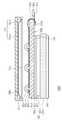
도 1a는 본 발명의 일 실시예에 따른 표시 장치에 대한 단면도이다.
도 1b는 본 발명의 일 실시예에 따른 표시 장치의 일부분에 대한 평면도이다.
도 2는 본 발명의 일 실시예에 따른 표시 장치의 상세도이다.
도 3는 본 발명의 일 실시예에 따른 하부 베이스 기판의 배면도이다.
도 4는 본 발명의 다른 일 실시예에 따른 표시 장치의 단면도이다.
도 5는 본 발명의 다른 일 실시예에 따른 표시 장치의 단면도이다.
도 6은 본 발명의 다른 일 실시예에 따른 표시 장치의 단면도이다.
도 7은 본 발명의 일 실시예에 따른 표시 장치 제조 방법의 순서도이다.
도 8은 도 7읜 S12 단계를 설명하기 위한 순서도이다.
도 9a 내지 도 9f는 도 7을 설명하기 위한 도면이다.1A is a cross-sectional view of a display device according to an embodiment of the present invention.
1B is a plan view of a portion of a display device according to an embodiment of the present invention.
2 is a detailed view of a display device according to an embodiment of the present invention.
3 is a rear view of a lower base substrate according to an embodiment of the present invention.
4 is a cross-sectional view of a display device according to another embodiment of the present invention.
5 is a cross-sectional view of a display device according to another embodiment of the present invention.
6 is a cross-sectional view of a display device according to another embodiment of the present invention.
7 is a flowchart of a method of manufacturing a display device according to an embodiment of the present invention.
8 is a flowchart for explaining the steps of FIG. 7 through S12.
Figs. 9A to 9F are views for explaining Fig. 7. Fig.
본 발명은 다양한 변경을 가할 수 있고 여러 가지 형태를 가질 수 있는 바, 특정 실시예들을 도면에 예시하고 본문에 상세하게 설명하고자 한다. 그러나, 이는 본 발명을 특정한 개시 형태에 대해 한정하려는 것이 아니며, 본 발명의 사상 및 기술 범위에 포함되는 모든 변경, 균등물 내지 대체물을 포함하는 것으로 이해되어야 한다.The present invention is capable of various modifications and various forms, and specific embodiments are illustrated in the drawings and described in detail in the text. It should be understood, however, that the invention is not intended to be limited to the particular forms disclosed, but includes all modifications, equivalents, and alternatives falling within the spirit and scope of the invention.
각 도면을 설명하면서 유사한 참조부호를 유사한 구성요소에 대해 사용하였다. 첨부된 도면에 있어서, 구조물들의 치수는 본 발명의 명확성을 위하여 실제보다 확대하여 도시한 것이다. 제1, 제2 등의 용어는 다양한 구성요소들을 설명하는데 사용될 수 있지만, 구성요소들은 용어들에 의해 한정되어서는 안 된다. 용어들은 하나의 구성요소를 다른 구성요소로부터 구별하는 목적으로만 사용된다. 예를 들어, 본 발명의 권리 범위를 벗어나지 않으면서 제1 구성요소는 제2 구성요소로 명명될 수 있고, 유사하게 제2 구성요소도 제1 구성요소로 명명될 수 있다. 단수의 표현은 문맥상 명백하게 다르게 뜻하지 않는 한, 다수의 표현을 포함한다. Like reference numerals are used for like elements in describing each drawing. In the accompanying drawings, the dimensions of the structures are shown enlarged from the actual for the sake of clarity of the present invention. The terms first, second, etc. may be used to describe various elements, but the elements should not be limited by terms. Terms are used only for the purpose of distinguishing one component from another. For example, without departing from the scope of the present invention, the first component may be referred to as a second component, and similarly, the second component may also be referred to as a first component. The singular forms "a," "an," and "the" include plural referents unless the context clearly dictates otherwise.
본 출원에서, "포함하다" 또는 "가지다" 등의 용어는 명세서 상에 기재된 특징, 숫자, 단계, 동작, 구성요소, 부품 또는 이들을 조합한 것이 존재함을 지정하려는 것이지, 하나 또는 그 이상의 다른 특징들이나 숫자, 단계, 동작, 구성요소, 부분품 또는 이들을 조합한 것들의 존재 또는 부가 가능성을 미리 배제하지 않는 것으로 이해되어야 한다. 또한, 층, 막, 영역, 판 등의 부분이 다른 부분 "위에" 또는 "상에" 있다고 할 경우, 이는 다른 부분 "바로 위에" 있는 경우뿐만 아니라 그 중간에 또 다른 부분이 있는 경우도 포함한다. 반대로 층, 막, 영역, 판 등의 부분이 다른 부분 "아래에" 있다고 할 경우, 이는 다른 부분 "바로 아래에" 있는 경우뿐만 아니라 그 중간에 또 다른 부분이 있는 경우도 포함한다.In the present application, the terms "comprises" or "having" and the like are used to specify that there is a feature, a number, a step, an operation, an element, a component or a combination thereof described in the specification, But do not preclude the presence or addition of one or more other features, integers, steps, operations, components, parts, or combinations thereof. Furthermore, when a part such as a layer, a film, an area, a plate, etc. is referred to as being "on" or "on" another part, it includes not only the case where it is "directly on" another part but also the case where there is another part in the middle . On the contrary, where a section such as a layer, a film, an area, a plate, etc. is referred to as being "under" another section, this includes not only the case where the section is "directly underneath"
이하, 첨부한 도면들을 참조하여 본 발명의 바람직한 실시예를 보다 상세하게 설명한다.Hereinafter, preferred embodiments of the present invention will be described in detail with reference to the accompanying drawings.
도 1a는 본 발명의 일 실시예에 따른 표시 장치에 대한 단면도이고, 도 1b는 본 발명의 일 실시예에 따른 표시 장치의 일부분에 대한 평면도이다.1A is a cross-sectional view of a display device according to an exemplary embodiment of the present invention, and FIG. 1B is a plan view of a portion of a display device according to an exemplary embodiment of the present invention.
도 1a를 참조하면, 본 발명의 일 실시예에 따른 표시 장치(1000)는 표시 패널(DP), 상부 편광판(101)을 포함할 수 있다.Referring to FIG. 1A, a
상기 표시 패널(DP)은 하부 기판(103), 액정층(120), 및 상부 기판(102)을 포함할 수 있다.The display panel DP may include a
상기 하부 기판(103)은 하부 베이스 기판(119), 화소층(122), 및 인셀 반사형 편광판(118)을 포함할 수 있다.The
상기 하부 베이스 기판(119)은 판 형상을 가질 수 있다. 상기 하부 베이스 기판(119)은 폴리이미드(PI; polyimide), 폴리에틸렌 테레프탈레이트(PET; polyethylene terephthalate), 폴리에틸렌 나프탈레이트(PEN; polyethylene naphtalate), 폴리카보네이트(PC; polycarbonate), 폴리아릴레이트(PAR; polyarylate), 폴리에테르이미드(PEI; polyetherimide), 폴리에테르술폰(PES; polyethersulphone) 및 섬유강화플라스틱(Fiber Reinforced Plastics) 등과 같이 내열성 및 내구성이 우수한 플라스틱을 소재로 만들어 질 수 있다. 그러나 본 발명은 이에 한정되지 않으며, 금속 포일이나 박막 유리(thin glass)와 같은 다양한 소재가 사용될 수 있다.The
상기 하부 베이스 기판(119) 상에는 제1 편광축(미도시)을 가지는 상기 인셀 반사형 편광판(118)이 배치될 수 있다. 상기 인셀 반사형 편광판(118)은 광을 수신하고, 수신 받은 광을 상기 제1 편광축과 평행한 방향으로 편광시킬 수 있다.On the
상기 인셀 반사형 편광판(118) 상에는 상기 화소층(122)이 배치될 수 있다.The
상기 화소층(122)은 게이트 전압에 응답하여 데이터 전압을 선택적으로 출력하는 박막 트랜지스터(TR, 도 2에 도시됨)를 포함할 수 있다.The
상기 인셀 반사형 편광판(118)과 상기 화소층(122)에 대해서는 도 2에서 자세하게 설명하도록 한다.The insular reflection
상기 하부 기판(103) 상측에는 상기 액정층(120)이 배치될 수 있다.The
상기 액정층(120)은 액정 분자(미도시)를 포함할 수 있다. 상기 액정 분자들은 상기 데이터 전압에 의해 형성된 전계에 의해서 제어될 수 있다.The
상기 액정층(120)의 가장자리에는 상기 액정 분자의 유출을 방지하기 위해 실런트(121)가 배치될 수 있다.A
상기 액정층(120)의 상측에는 상기 상부 기판(102)이 배치될 수 있다.The
상기 상부 기판(102)은 광원으로부터 제공되는 광을 이용하여 소정의 색을 구현하는 컬러 필터(미도시)를 포함할 수 있다.The
상기 상부 기판(102) 상측에는 상기 상부 편광판(101)이 배치될 수 있다.The
상기 상부 편광판(101)은 제2 편광축(미도시)을 가질 수 있다. 상기 상부 편광판(101)은 광을 수신하고, 수신 받은 광은 상기 제2 편광축과 평행한 방향으로 편광시킬 수 있다.The
본 발명의 일 실시예에 따른 상기 표시 장치(1000)는 광원(105), 광원 구동 전극(104), 확산판(113), 반사판(111), 및 바텀 샤시(112)를 더 포함할 수 있다.The
상기 하부 베이스 기판(119)의 하면에는 상기 광원(105)이 실장될 수 있다.The
도 1a에 도시된 것처럼 상기 광원(105)은 복수로 제공될 수 있다. 상기 광원들(105)은 상기 표시 패널(DP)이 영상을 출력하기 위한 광을 출력할 수 있다. 본 발명의 일 예에서 상기 광원들(105)은 상기 반사판(111) 측으로 광을 출력할 수 있다.As shown in FIG. 1A, the
본 발명의 일 예에서, 상기 광원은 예를 들어 LED(light emitting diode) 광원일 수 있다. 상기 LED 광원은 예를 들어, 백색광을 생성할 수 있다. 상기 LED 광원은 청색, 적색, 녹색을 생성할 수도 있다.In one example of the present invention, the light source may be, for example, a light emitting diode (LED) light source. The LED light source may generate, for example, white light. The LED light source may generate blue, red, and green.
상기 커버 렌즈(106)는 소정의 굴절률을 가지는 부재일 수 있다. 커버 렌즈들(106)은 돔(dome) 형상을 가질 수 있다. 상기 커버 렌즈들(106)은 각각 상기 광원들(105)을 커버할 수 있다.The
상기 커버 렌즈(106)는 상기 광원들(105)에서 출력되는 광이 고르게 분산되도록 상기 광원에서 출력되는 광을 굴절시킬 수 있다.The
상기 광원 구동 전극(104)은 상기 하부 베이스 기판(119) 하면에 배치될 수 있다.The light
상기 광원 구동 전극(104)은 상기 광원들(105)을 연결할 수 있다.The light
상기 광원 구동 전극(104)은 상기 광원이 구동될 수 있도록 구동 신호 및 전력을 공급할 수 있다.The light
상기 광원들(105) 하측에는 상기 확산판(113)이 배치될 수 있다.The
상기 확산판(113)은 판 형상을 가지며, 상기 광원들(105)로부터 출력된 광을 하측을 확산시킬 수 있다.The
상기 확산판(113) 하측에는 상기 반사판(111)이 배치될 수 있다.The
상기 반사판(111)에는 중앙부(111a)와 가장자리부(111b)가 정의될 수 있다.The
상기 중앙부(111a)는 평평한 판 형상을 가질 수 있다. 상기 가장자리부(111b)는 상기 중앙부(111a)로부터 기울어져 연장될 수 있다. 좀 더 상세하게 설명하면 상기 가장자리부(111b)는 상기 중앙부(111a)과 소정의 각도(ANG)를 이룰 수 있다. 상기 소정의 각도(ANG)는 둔각일 수 있다.The
상기 가장자리부(111b)와 상기 중앙부(111a)는 상기 소정의 각도(ANG)를 형성하여, 상기 가장자리부(111b) 측으로 이동하는 광을 상기 중앙부(111a) 측으로 반사시킴으로써, 광이 표시 패널의 측면으로 새어나가는 것을 방지할 수 있다.The
상기 바텀 샤시(112)에는 수납 공간이 정의될 수 있다. 예를 들어 본 발명의 일 예에서 상기 바텀 샤시(112)에는 상기 확산판(113)과 상기 반사판(111)이 상기 수납 공간에 수납될 수 있다.A storage space may be defined in the
상기 수납 공간에 상기 확산판(113), 상기 반사판(111) 및 상기 표시 패널(100)과 같은 구성들이 수납됨으로써, 상기 바텀샤시는 외부로부터 충격을 흡수하여 상기 수납 공간에 수납된 구성들을 외부의 충격으로부터 보호할 수 있다.The bottom chassis receives the impacts from the outside and stores the components stored in the storage space in the storage space to the exterior It can protect against impact.
도 1a 및 1b를 참조하면, 본 발명의 일 실시예에 따른 표시 장치는 광원 배선 필름(107), 제1 내지 제 6 패드부(Pad1 ~ Pad6), 연결 필름(110), 인쇄 회로 기판(109), 및 제2 광원 구동 배선(DC2), 및 제2 광원 전원 배선(PC2)을 더 포함할 수 있다.1A and 1B, a display device according to an embodiment of the present invention includes a light
상기 광원 배선 필름(107)은 베이스 필름(BF), 제1 광원 구동 배선(DC1), 및 제1 광원 전원 배선(PC1)을 포함할 수 있다.The light
상기 베이스 필름(BF)의 일단은 상기 하부 베이스 기판(119)의 하면에 부착될 수 있고, 상기 베이스 필름(BF)의 타단은 상기 하부 베이스 기판(119) 상면에 부착될 수 있다. 좀 더 상세하게 설명하면 상기 베이스 필름(BF)의 타단은 상기 하부 베이스 기판(119) 상면의 가장자리 영역(EDA)에 부착될 수 있다.One end of the base film BF may be attached to the lower surface of the
상기 제1 및 제2 패드부(Pad1, Pad2)는 상기 가장자리 영역(EDA)에 형성될 수 있다.The first and second pad portions Pad1 and Pad2 may be formed in the edge region EDA.
상기 제1 광원 구동 배선(DC1)은 상기 베이스 필름(BF) 상에 배치될 수 있다.The first light source driving wiring DC1 may be disposed on the base film BF.
상기 제1 광원 구동 배선(DC1)은 상기 제1 패드부(Pad1)와 상기 광원 구동 전극(104)을 전기적으로 연결하는 배선일 수 있다.The first light source driving wiring DC1 may be a wiring for electrically connecting the first pad unit Pad1 and the light
상기 제1 광원 전원 배선(PC1)은 상기 베이스 필름(BF) 상에 배치될 수 있다.The first light source power supply line PC1 may be disposed on the base film BF.
도 1b에서는 생략되었지만 상기 베이스 필름(BF) 상에는 상기 제1 광원 전원 배선(PC1) 및 상기 제1 광원 구동 배선(DC1)을 커버하는 광원 배선 커버 필름(미도시)이 배치될 수 있다.Although not shown in FIG. 1B, a light source wiring cover film (not shown) covering the first light source power wiring PC1 and the first light source driving wiring DC1 may be disposed on the base film BF.
상기 제1 광원 전원 배선(PC1)은 상기 제2 패드부(Pad2)와 상기 광원 구동 전극(104)을 전기적으로 연결하는 배선일 수 있다.The first light source power line PC1 may be a line that electrically connects the second pad unit Pad2 and the light
도 1b에는 도시되지 않았지만, 상기 베이스 필름(BF) 상에는 광원 제어부(미도시)가 배치될 수 있다.Although not shown in FIG. 1B, a light source control unit (not shown) may be disposed on the base film BF.
상기 광원 제어부는 상기 제1 광원 구동 배선(DC1) 및 상기 제1 광원 전원 배선(PC1)과 전기적으로 연결될 수 있다.The light source control unit may be electrically connected to the first light source driving line DC1 and the first light source power line PC1.
상기 광원 제어부는 상기 제1 광원 구동 배선(DC1)으로부터 후술할 광원 제어 신호 및 상기 제1 광원 전원 배선(PC1)으로부터 상기 광원들(105)를 구동시키는 구동 전력을 수신받아 상기 광원 구동 전극(104)을 통해 상기 광원들(105)에게 전달할 수 있다.The light source control unit receives the light source control signal to be described later from the first light source driving line DC1 and the driving power for driving the
상기 제3 및 제4 패드부(Pad3, Pad4)는 상기 가장자리 영역(EDA)에 형성될 수 있다.The third and fourth pad portions Pad3 and Pad4 may be formed in the edge region EDA.
상기 제5 및 제6 패드부(Pad5, Pad6)는 상기 인쇄 회로 기판(109) 상에 형성될 수 있다.The fifth and sixth pad portions (Pad5, Pad6) may be formed on the printed circuit board (109).
상기 연결 필름(110)은 상기 인쇄 회로 기판(109)과 상기 가장자리 영역(EDA)을 연결하는 필름일 수 있다. 상기 연결 필름(110)의 일단은 상기 가장자리 영역(EDA) 상에 부착될 수 있고, 상기 연결 필름(110)의 타단은 상기 인쇄 회로 기판(109) 상에 부착될 수 있다. 본 발명의 일 예에서 상기 연결 필름(110)에는 COF(chips on film)을 통해 반도체 칩이 장착될 수 있다. 다만 상기 연결 필름(110)은 이에 한정되지 않고, 다양한 형태로 반도체 칩이 상기 연결 필름(110)에 장착될 수 있다.The
상기 인쇄 회로 기판(109) 상에는 상기 구동부(TCON)와 상기 전원 공급부(PIC)가 배치될 수 있다.The driving unit (TCON) and the power supply unit (PIC) may be disposed on the printed circuit board (109).
상기 제2 광원 구동 배선(DC2)은 상기 제1 패드부(Pad1)와 상기 구동부(TCON)를 연결할 수 있다.The second light source driving line DC2 may connect the first pad Pad1 and the driving unit TCON.
상기 제2 광원 구동 배선(DC2)은 제1 구동 연결부(DC2a), 제2 구동 연결부(DC2b), 및 제3 구동 연결부(DC2c)를 포함할 수 있다.The second light source driving line DC2 may include a first driving connection DC2a, a second driving connection DC2b, and a third driving connection DC2c.
상기 제1 구동 연결부(DC2a)는 상기 연결 필름(110) 상에 배치될 수 있다.The first driving connection portion DC2a may be disposed on the
도 1b에서는 생략되었지만 상기 연결 필름(110) 상에는 상기 제1 구동 연결부(DC2a)를 커버하는 연결부 커버 필름(미도시)이 배치될 수 있다.Although not shown in FIG. 1B, a connection cover film (not shown) covering the first driving connection portion DC2a may be disposed on the
상기 제1 구동 연결부(DC2a)의 일단은 상기 제3 패드부(Pad3)와 연결될 수 있고, 상기 제1 구동 연결부(DC2a)의 타단은 상기 제5 패드부(Pad5)를 연결할 수 있다.One end of the first drive connection part DC2a may be connected to the third pad part Pad3 and the other end of the first drive connection part DC2a may connect the fifth pad part Pad5.
상기 제2 구동 연결부(DC2b)는 상기 가장자리 영역(EDA)에 배치될 수 있다.The second driving connection part DC2b may be disposed in the edge area EDA.
상기 제2 구동 연결부(DC2b)의 일단은 상기 제1 패드부(Pad1)와 연결될 수 있고, 상기 제2 구동 연결부(DC2b)의 타단은 상기 제3 패드부(Pad3)와 연결될 수 있다. 즉 상기 제2 구동 연결부(DC2b)의 타단은 상기 제1 구동 연결부(DC2a)와 전기적으로 연결될 수 있다.One end of the second driving connection part DC2b may be connected to the first pad part Pad1 and the other end of the second driving connection part DC2b may be connected to the third pad part Pad3. That is, the other end of the second drive connection part DC2b may be electrically connected to the first drive connection part DC2a.
상기 제3 구동 연결부(DC2c)는 상기 인쇄 회로 기판(109) 상에 배치될 수 있다.The third drive connection DC2c may be disposed on the printed
상기 제3 구동 연결부(DC2c)의 일단은 상기 구동부(TCON)와 연결될 수 있고, 상기 제3 구동 연결부(DC2c)의 타단은 상기 제5 패드부(Pad5)와 연결될 수 있다. 즉 상기 제3 구동 연결부(DC2c)의 타단은 상기 제1 구동 연결부(DC2a)와 전기적으로 연결될 수 있다One end of the third drive connection part DC2c may be connected to the driving part TCON and the other end of the third drive connection part DC2c may be connected to the fifth pad part Pad5. That is, the other end of the third drive connection DC2c may be electrically connected to the first drive connection DC2a
상기 제2 광원 전원 배선(PC2)은 상기 제2 패드부(Pad2)와 상기 전원 공급부(PIC)를 연결할 수 있다.The second light source power line PC2 may connect the second pad Pad2 to the power supply line PIC.
상기 제2 광원 전원 배선(PC2)은 제1 전원 연결부(PC2a), 제2 전원 연결부(PC2b), 및 제3 전원 연결부(PC2c)를 포함할 수 있다.The second light source power line PC2 may include a first power connection PC2a, a second power connection PC2b, and a third power connection PC2c.
상기 제1 전원 연결부(PC2a)는 상기 연결 필름(110) 상에 배치될 수 있다.The first power connection part PC2a may be disposed on the
상기 제1 전원 연결부(PC2a)의 일단은 상기 재4 패드부(Pad4)와 연결될 수 있고, 상기 제1 구동 연결부(DC2a)의 타단은 상기 제6 패드부(Pad6)를 연결할 수 있다.One end of the first power connection part PC2a may be connected to the pad 4 and the other end of the first driving connection part DC2a may connect the sixth pad part Pad6.
상기 제2 전원 연결부(PC2b)는 상기 가장자리 영역(EDA)에 배치될 수 있다.The second power connection part PC2b may be disposed in the edge area EDA.
상기 제2 전원 연결부(PC2b)의 일단은 상기 제2 패드부(Pad2)와 연결될 수 있고, 상기 제2 전원 연결부(PC2b)의 타단은 상기 제4 패드부(Pad4)와 연결될 수 있다. 즉 상기 제2 전원 연결부(PC2b)의 타단은 상기 제1 전원 연결부(PC2a)와 전기적으로 연결될 수 있다.One end of the second power connection part PC2b may be connected to the second pad part Pad2 and the other end of the second power connection part PC2b may be connected to the fourth pad part Pad4. That is, the other end of the second power connection part PC2b may be electrically connected to the first power connection part PC2a.
상기 제3 전원 연결부(PC2c)는 상기 인쇄 회로 기판(109) 상에 배치될 수 있다.The third power connection PC2c may be disposed on the printed
상기 제3 전원 연결부(PC2c)의 일단은 상기 전원 공급부(PIC)와 연결될 수 있고, 상기 제3 전원 연결부(PC2c)의 타단은 상기 제6 패드부(Pad6)와 연결될 수 있다. 즉 상기 제3 전원 연결부(PC2c)의 타단은 상기 제1 전원 연결부(PC2a)와 전기적으로 연결될 수 있다One end of the third power connection part PC2c may be connected to the power supply part PIC and the other end of the third power connection part PC2c may be connected to the sixth pad part Pad6. That is, the other end of the third power connection PC2c may be electrically connected to the first power connection PC2a
상기 구동부(TCON)는 상기 표시 패널(DP)을 제어하는 패널 구동부(미도시) 및 상기 광원들을 제어하는 광원 구동부(미도시)를 포함할 수 있다. 상기 패널 구동부는 상기 표시 패널을 제어하기 위한 패널 제어 신호를 상기 연결 필름(110)에 출력 할 수 있다. 상기 패널 제어 신호는 예를 들어, 게이트 제어 신호 또는 데이터 제어 신호와 같이 드라이버를 제어하는 신호일 수 있다.The driving unit TCON may include a panel driver (not shown) for controlling the display panel DP and a light source driver (not shown) for controlling the light sources. The panel driving unit may output a panel control signal for controlling the display panel to the
나아가, 상기 광원 구동부는 상기 제1 광원 구동 배선(DC1) 및 상기 제2 광원 구동 배선(DC2)을 통해 상기 광원들(105)을 제어하기 위한 상기 광원 제어 신호를 출력할 수 있다.Furthermore, the light source driving unit may output the light source control signal for controlling the
상기 광원 구동부는 상기 패널 구동부와 함께 상기 인쇄회로기판에 실장/구현될 수 있으며, 상기 광원 제어 신호는 상기 패널 제어 신호와 함께 상기 연결 필름을 통해 출력될 수 있다. 본 발명의 일 예에서, 상기 광원 구동부를 위한 별도의 인쇄 회로 기판 또는 별도의 연결 필름이 요구되지 않는다.The light source driving unit may be mounted on the printed circuit board together with the panel driving unit, and the light source control signal may be output through the connecting film together with the panel control signal. In an embodiment of the present invention, a separate printed circuit board or a separate connection film for the light source driver is not required.
상기 전원 공급부(PIC)는 상기 표시 패널(DP)을 구동시키는 구동 전력을 생성할 수 있다. 나아가 상기 전원 공급부(PIC)는 상기 제1 광원 전원 배선(PC1) 및 상기 제2 광원 전원 배선(PC2)과 연결되어 상기 광원들(105)을 구동시키는 구동 전력을 생성할 수 있다.The power supply unit PIC may generate driving power for driving the display panel DP. Furthermore, the power supply unit PIC may be connected to the first light source power line PC1 and the second light source power line PC2 to generate driving power for driving the
결론적으로 상기 하부 베이스 기판(119) 하면에 상기 광원들(105)을 실장함에 따라 표시 장치를 구현하기 위한 부품을 줄일 수 있고, 제조 원가 절감의 효과를 가져올 수 있다.As a result, since the
도 2는 본 발명의 일 실시예에 따른 표시 장치의 상세도이다.2 is a detailed view of a display device according to an embodiment of the present invention.
도 2를 참조하면, 상기 광원(105)으로부터 출력되는 제1 광(L1)은 상기 커버 렌즈(106)에 의해서 굴절될 수 있다. 상기 커버 렌즈(106)에 의해서 굴절된 상기 제1 광(L1)을 제2 광(L2)으로 지시한다.Referring to FIG. 2, the first light L1 output from the
상기 제2 광(L2)은 상기 확산판(113)에 의해서 확산될 수 있다. 상기 확산판(113)은 상기 제2 광(L2)을 제3 광으로 확산시킬 수 있다.The second light L2 may be diffused by the
확산판(113)을 통과한 상기 제3 광(L3)은 상기 반사판(111)에 의해서 상측으로 반사된다.The third light L3 having passed through the
상기 확산판(113)을 통과한 상기 제3 광(L3)은 상기 반사판(111)에 의해서 상측으로 반사된다.The third light (L3) having passed through the diffuser plate (113) is reflected upward by the reflector (111).
반사된 상기 제3 광(L3)을 제4 광(L4)으로 지시한다.And directs the reflected third light L3 as the fourth light L4.
상기 제4 광(L4)은 상측으로 이동하여, 상기 확산판(113)에 의해서 재차 확산될 수 있다.The fourth light L4 may move upward and be diffused again by the
상기 재차 확산된 상기 제4 광(L4)은 제5 광(L5)으로 지시한다.The fourth light L4 diffused again is indicated by the fifth light L5.
상기 제5 광(L5)은 상기 광원 구동 전극(104)을 통과하는 광일 수 있다.The fifth light (L5) may be light passing through the light source driving electrode (104).
상기 광원 구동 전극(104)은 투명 전극 또는 반투명 전극일 수 있다. 이 경우 상기 제5 광(L5)은 그 휘도의 감쇠 없이 상기 광원 구동 전극(104)을 통과할 수 있다The light
상기 제5 광(L5)은 상기 하부 베이스 기판(119) 내부에서 확산되며 진행할 수 있다. 상기 하부 베이스 기판(119) 내부의 상기 제5 광(L5)을 제6 광(L6)으로 지시한다.The fifth light L5 diffuses in the
상기 제6 광(L6)은 상기 하부 베이스 기판(119) 내부를 통해서 상측으로 이동할 수 있다. 상기 제6 광(L6)은 상측으로 이동하여, 상기 인셀 반사형 편광판(118)에 의해서 편광될 수 있다.The sixth light L6 may move upward through the inside of the
좀 더 상세하게 설명하면, 상기 인셀 반사형 편광판(118)은 상기 제1 편광축과 평행한 방향으로 상기 제6 광(L6)을 편광시킬 수 있다.In more detail, the Incel
본 발명의 일 예에서 상기 표시 패널(DP)은 표시 영역(DA) 및 비표시 영역(NDA)으로 구분될 수 있다.In an exemplary embodiment of the present invention, the display panel DP may be divided into a display area DA and a non-display area NDA.
상기 인셀 반사형 편광판(118)은 상기 표시 영역(DA)에 대응하여 상기 하부 베이스 기판(119) 상에 구비되는 복수의 와이어 그리드 패턴(215) 및 상기 비표시 영역(NDA)에 대응하여 상기 하부 베이스 기판(119) 상에 구비된 반사 패턴(214)을 더 포함할 수 있다. 상기 복수의 와이어 그리드 패턴(215) 및 반사 패턴(214)은 예를 들어 알루미늄, 구리등과 같은 금속들을 포함할 수 있다.The incandescent
상기 와이어 그리드 패턴들(215)은 상기 제6 광(L6) 중 상기 와이어 그리드 패턴들(215)의 연장 방향과 평행한 성분은 상기 와이어 그리드 패턴들(215)의에 의해서 반사될 수 있다.The
그리고 상기 제6 광(L6) 중 상기 와이어 그리드 패턴들(215)의 연장 방향과 직교하는 방향과 평행한 성분은 유효 굴절 매질로 인식되어 투과될 수 있다. 즉 상기 제6 광(L6) 중 상기 제1 편광축과 평행한 성분은 상기 인셀 반사형 편광판(118)을 통과 할 수 있다.A component of the sixth light L6 parallel to the direction perpendicular to the extending direction of the
따라서 상기 제6 광(L6) 중 상기 반사 패턴(214)에 인접한 곳으로 이동한 제6 광(L6)은 상기 반사 패턴(214)에 의해서 하측으로 반사될 수 있다. 하측으로 반사된 상기 제6 광(L6)은 전술한 광의 이동과정(상기 제1 광(L1)에서 상기 제6 광(L6)이 되는 과정)에 의해서 다시 상측으로 이동되어, 상기 인셀 반사형 편광판(118)에 의해서 편광될 수 있다. 따라서 상기 반사 패턴(214)에 의해서 상기 광 이용 효율을 향상시킬 수 잇다.Accordingly, the sixth light (L6) of the sixth light (L6) moved to a position adjacent to the reflection pattern (214) may be reflected downward by the reflection pattern (214). The sixth light L6 reflected downward is further moved upward by the movement of the light (the process of changing from the first light L1 to the sixth light L6) And can be polarized by the
전술한 바와 같이, 상기 광원들(105)은 상기 표시 패널(DP)의 하측으로 광을 출력하고, 상기 출력된 광이 상기 반사판(111)에 의해서 상측으로 반사되므로, 상기 광원(105)에서 출력된 광의 이동거리가 증가할 수 있다.As described above, the
즉, 도 2에서 광학 거리(OD)를 늘릴수록 상기 광원들(105)에서 출력된 광의 이동 거리가 상기 광학 거리(OD)의 2배로 늘어날 수 있어, 광이 효과적으로 확산될 수 있다. 따라서 상기 표시 장치의 휘도 균일성이 향상될 수 있다.That is, in FIG. 2, as the optical distance OD increases, the moving distance of the light output from the
나아가 상기 광원들(105) 간의 거리로 정의되는 피치(PIT)를 상기 광학 거리(OD)와 동시에 조절함으로써, 적절한 면광원 구현과 동시에 상기 표시 장치의 슬림화를 구현할 수 있다.Further, by simultaneously adjusting the pitch PIT defined by the distance between the
이하 상기 인셀 반사형 편광판(118) 상측의 구성에 대해서 설명하도록 한다.Hereinafter, the configuration on the upper side of the above-mentioned incandescence reflective
도 2를 참조하면, 상기 인셀 반사형 편광판(118)의 상면에는 베이스 절연막(216)이 형성된다. 상기 베이스 절연막(216)은 상기 반사 패턴(214) 및 상기 와이어 그리드 패턴들(215)을 커버할 수 있다.Referring to FIG. 2, a
상기 베이스 절연막(216)은 상기 반사 패턴(214) 및 상기 와이어 그리드 패턴들(215)을 상기 화소층(122)과 전기적으로 절연시키기 위하여 절연성 물질을 포함할 수 있다.The
상기 화소층(122)은 상기 박막 트랜지스터(TR), 층간 절연막(208), 및 화소 전극(207)을 포함할 수 있다. 상기 박막 트랜지스터(TR)는 게이트 전극(220), 소스 전극(212), 및 드레인 전극(210)을 포함할 수 있다.The
상기 베이스 절연막(216) 상에는 상기 게이트 전극(220)이 형성될 수 있다. 상기 게이트 전극(220)은 게이트 절연막(213)에 의해서 커버될 수 있다. 상기 게이트 전극(220)에 대응하여 상기 게이트 절연막(213) 상에는 반도체층(211)이 형성될 수 있다. 상기 반도체층(211) 상에는 상기 소스 전극(212) 및 상기 드레인 전극(210)이 소정의 간격으로 이격되어 배치될 수 있다.The
상기 층간 절연막(208)은 상기 게이트 절연막(213) 상에 형성되어 상기 박막 트랜지스터(TR)를 커버할 수 있다. 상기 층간 절연막(208) 상측에는 상기 화소 전극(207)이 형성될 수 있다.The interlayer insulating
상기 층간 절연막(208)에는 상기 박막 트랜지스터(TR)의 상기 드레인 전극(210)을 노출시키는 컨택홀(206a)이 형성될 수 있다. 상기 컨택홀(206a)을 통해 상기 화소 전극(207)은 상기 드레인 전극(210)과 전기적으로 연결될 수 있다.A
상기 상부 기판(102)은 상부 베이스 기판(201), 컬러 필터층(202), 및 블랙 매트릭스(203)를 포함할 수 있다. 상기 상부 베이스 기판(201)은 판 형상을 가질 수 있다. 상기 상부 베이스 기판(201)은 폴리이미드(PI; polyimide), 폴리에틸렌 테레프탈레이트(PET; polyethylene terephthalate), 폴리에틸렌 나프탈레이트(PEN; polyethylene naphtalate), 폴리카보네이트(PC; polycarbonate), 폴리아릴레이트(PAR; polyarylate), 폴리에테르이미드(PEI; polyetherimide), 폴리에테르술폰(PES; polyethersulphone) 및 섬유강화플라스틱(Fiber Reinforced Plastics) 등과 같이 내열성 및 내구성이 우수한 플라스틱을 소재로 만들어 질 수 있다. 그러나 본 발명은 이에 한정되지 않으며, 금속 포일이나 박막 유리(thin glass)와 같은 다양한 소재가 사용될 수 있다.The
상기 상부 베이스 기판(201)은 상기 하부 베이스 기판(119)과 대향하여 배치될 수 있다.The
상기 블랙 매트릭스(203)는 상기 비표시 영역(NDA)에 대응하여 상기 상부 베이스 기판(201) 상에 배치될 수 있다. 상기 컬러 필터층(202)은 레드, 그린, 및 블루 색화소를 포함하고, 각 색화소들은 적어도 상기 표시 영역(DA)에 대응하고, 상기 블랙 매트릭스(203)와는 중첩될 수 있다.The
상기 상부 기판(102)과 상기 하부 기판(103) 사이에는 상기 액정층(120)이 배치될 수 있다.The
상기 표시 패널(DP)은 상기 상부 기판(102)과 상기 하부 기판(103) 사이에 상기 액정층(120)이 형성될 공간을 제공하기 위하여 상기 상부 기판(102)과 상기 하부 기판(103)을 소정 간격 이격시키는 스페이서(205)를 더 포함할 수 있다.The display panel DP is formed between the
상기 표시 패널(DP) 상에는 상기 상부 편광판(101)이 배치될 수 있다.The
상기 상부 편광판(101)은 시트 또는 필름 형태를 가지며, 상기 표시 패널(DP)에 상에 부착될 수 있다.The
상기 상부 편광판(101)의 상기 제2 편광축은 상기 인셀 반사형 편광판(118)의 상기 제1 편광축과 수직할 수 있다.The second polarizing axis of the
도 3는 본 발명의 일 실시예에 따른 하부 베이스 기판의 배면도이다.3 is a rear view of a lower base substrate according to an embodiment of the present invention.
도 3을 참조하면, 상기 하부 베이스 기판(119)의 하면에는 상기 광원들(105)이 각각 소정의 간격으로 이격되어 배치될 수 있다.Referring to FIG. 3, the
도 3에서 상기 광원들(105)은 제1 방향(DR1) 및 상기 제1 방향(DR1)과 수직한 제2 방향(DR2)과 각각 평행한 3행(R1~R3) 및 4열(C1~C4)의 매트릭스 형태로 배열되는 3x4개의 상기 광원들(105)로 도시될 수 있다.3, the
도 3에서는 3x4의 매트릭스 형태의 광원들(105)을 도시하였지만, 이에 한정되지 않으며 다양한 형태로 상기 하부 베이스 기판(119)에 상기 광원들(105)은 실장될 수 있다.3, the
도 3를 참조하면, 상기 제1 행(R1)의 광원들(105)은 상기 광원 구동 전극(104)을 통해 상기 제1 방향(DR1)으로 나란하게 연결될 수 있다. 상기 제1 행(R1) 및 상기 제4 열(C4)에 대응되는 광원은 상기 제2 행(R2) 및 상기 제4 열(C4)에 대응되는 광원과 상기 광원 구동 전극(104)을 통해서 연결될 수 있다.Referring to FIG. 3, the
상기 제2 행의 광원들(105)은 상기 광원 구동 전극(104)을 통해서 상기 제1 방향(DR1)으로 나란하게 연결될 수 있다. 상기 제2 행(R2) 및 상기 제1 열(C1)에 대응되는 광원은 상기 제3 행(R3) 및 상기 제1 열(C1)에 대응되는 광원과 상기 광원 구동 전극(104)을 통해서 상기 제2 방향(DR2)으로 연결될 수 있다.The
상기 제3 행의 광원들(105)은 상기 광원 구동 전극(104)을 통해서 상기 제1 방향(DR1)으로 나란하게 연결될 수 있다.The
따라서 도 3에 도시된 상기 광원들(105)은 상기 광원 구동 전극(104)을 통해서 직렬로 연결될 수 있다.Therefore, the
그리고 상기 제1 행(R1) 및 상기 제1 열(C1)에 대응되는 광원과 상기 제3 행(R3) 및 상기 제4 열(C4)에 대응되는 광원은 상기 광원 구동 전극(104)을 통해서 연결될 수 있고, 상기 제1 행(R1) 및 상기 제1 열(C1)에 대응되는 광원과 상기 제3 행(R3) 및 상기 제4 열(C4)에 대응되는 광원을 연결하는 광원 구동 전극은(104) 소정의 배선을 통해서 상기 광원 제어부와 연결될 수 있다.A light source corresponding to the first row R1 and the first column C1 and a light source corresponding to the third row R3 and the fourth column C4 are connected to the light
즉, 도 1b 및 도 3을 참조하면 상기 광원들(105)은 상기 제1 행(R1) 및 상기 제1 열(C1)에 대응되는 광원과 상기 제3 행(R3) 및 상기 제4 열(C4)에 대응되는 광원을 연결하는 광원 구동 전극은(104) 상기 광원 제어 신호 및 상기 제1 광원 전원 배선(PC1)으로부터 상기 광원들(105)를 구동시키는 상기 구동 전력을 수신받을 수 있다.1B and 3, the
도 4는 본 발명의 다른 일 실시예에 따른 표시 장치의 단면도이다.4 is a cross-sectional view of a display device according to another embodiment of the present invention.
도 4를 참조하면, 상기 하부 베이스 기판(119)의 가장자리에 필름 홀(401)이 정의될 수 있다. 상기 필름 홀(401)을 통해서 상기 광원 배선 필름(107')은 상기 하부 베이스 기판(119) 하면과 상기 가장자리 영역(EDA)를 연결할 수 있다.Referring to FIG. 4, a film hole 401 may be defined at the edge of the
상기 필름 홀(401)에 상기 광원 배선 필름(107')을 삽입하여 상기 광원 배선 필름(107')이 상기 하부 베이스 기판(119)의 하면과 상기 가장자리 영역(EDA)를 연결함으로써, 표시 장치의 슬림화를 구현할 수 있다.The light source wiring film 107 'is inserted into the film hole 401 so that the lower surface of the
나머지 구성에 대해서는 도 1에 도시된 것과 동일하므로 생략하도록 한다.The rest of the configuration is the same as that shown in Fig. 1 and will be omitted.
도 5는 본 발명의 다른 일 실시예에 따른 표시 장치의 단면도이다.5 is a cross-sectional view of a display device according to another embodiment of the present invention.
도 5를 참조하면, 상기 하부 기판(103)은 확산 입자(501)를 더 구비할 수 있다. 상기 확산 입자(501)는 상기 하부 베이스 기판(119) 내에 구비될 수 있다.Referring to FIG. 5, the
상기 확산 입자(501)는 광을 산란 또는 반사시킬 수 있다.The
상기 하부 베이스 기판(119)의 굴절률과 상기 확산 입자(501)의 굴절률은 상이할 수 있다. 본 발명의 일 예에서 상기 하부 베이스 기판(119)의 굴절률은 상기 확산 입자(501)의 굴절률보다 더 클 수 있다.The refractive index of the
상기 확산 입자(501)는 상기 하부 베이스 기판(119)의 제조 도중에 첨가될 수 있다. 상기 확산 입자(501)의 일 예로, PMMA(Poly Methyl Meth Acrylate) 재질로 이루어질 수 있고, 비드(Bead) 형태를 가질 수 있다. 다만 상기 확산 입자(501)는 이에 한정되지 않는다.The
상기 확산 입자(501)가 상기 하부 베이스 기판(119) 내에 구비됨으로써, 상기 하부 베이스 기판(119)을 통해 출사되는 광을 더 확산시켜, 상기 표시 패널(DP)이 표시하는 영상의 휘도 균일성을 도모할 수 있다.The
나머지 구성에 대해서는 도 1에 도시된 것과 동일하므로 생략하도록 한다.The rest of the configuration is the same as that shown in Fig. 1 and will be omitted.
도 6은 본 발명의 다른 일 실시예에 따른 표시 장치의 단면도이다.6 is a cross-sectional view of a display device according to another embodiment of the present invention.
도 6을 참조하면 표시 장치(1000')는 확산 부재(601)를 더 포함할 수 있다.Referring to FIG. 6, the display device 1000 'may further include a
상기 확산 부재(601)는 상기 광원 구동 전극(104)의 하면에 배치될 수 있다.The
상기 확산 부재(601)는 상기 광원 구동 전극(104)의 하면에 배치됨으로써, 상기 하부 베이스 기판(119) 하면에는 광원 홀(602)이 정의될 수 있다.The
상기 광원들(105)은 상기 광원 홀들(602)에 각각 삽입될 수 있다.The
본 발명의 일 예에서, 상기 확산 부재(601)는 광을 산란 반사시키는 상기 확산 입자를 포함할 수 있다.In one example of the present invention, the
상기 확산 부재(601)가 상기 광원 구동 전극(104)의 하면에 배치됨으로써, 표시 패널(DP) 측으로 출사되는 광을 더욱 확산시켜 상기 표시 패널(DP)이 표시하는 영상의 휘도 균일성을 도모할 수 있다.The
도 7은 본 발명의 일 실시예에 따른 표시 장치 제조 방법의 순서도이고, 도 8은 도 7읜 S12 단계를 설명하기 위한 순서도이고, 도 9a 내지 도 9f는 도 7을 설명하기 위한 도면이다.FIG. 7 is a flowchart illustrating a method of manufacturing a display device according to an embodiment of the present invention. FIG. 8 is a flow chart for explaining the steps of FIG. 7 and S12. FIGS. 9A to 9F are views for explaining FIG.
도 7 및 도 9a을 참조하면, 먼저 본 발명의 일 실시예에 따를 표시 장치를 제조하기 위하여, 하부 베이스 기판(119)을 제공할 수 있다.(S11) 다음으로 상기 하부 베이스 기판(119) 하면에 광원 구동 전극(104)을 형성할 수 있다.(S12)Referring to FIGS. 7 and 9A, a
도 8, 도 9b, 및 도 9c를 참조하면 상기 광원 구동 전극(104)을 형성하기 위해서 먼저 상기 하부 베이스 기판(119)의 하면에 도전층(901)을 형성할 수 있다.(S21) 상기 도전층(901)은 전기 전도성이 우수한 금속 물질을 포함할 수 있다. 다음으로 상기 광원 구동 전극(104)을 형성하기 위해서 상기 도전층(901)을 패터닝할 수 있다.(S22) 본 발명의 일 예로, 상기 광원 구동 전극(104)들은 상기 하부 베이스 기판(119) 하면에 ITO(indium tin oxide)층을 형성하고, 포토 리소그래피(photo lithography) 과정을 통해서 형성될 수 있다.8, 9B, and 9C, a
도 7 및 도 9d를 참조하면, 상기 광원 구동 전극(104)이 형성한 후 상기 광원(105)을 실장할 수 있다.(S13) 상기 광원(105)은 복수개로 제공될 수 있으며, 상기 광원들(105)은 상기 광원 구동 전극(104)에 의해서 서로 전기적으로 연결되도록 상기 하부 베이스 기판(119) 하면에 실장될 수 있다.7 and 9D, the
다음으로 도 7 및 도 9e를 참조하면, 상기 광원들(105) 하측에 반사판(111)을 배치할 수 있다.(S14) 상기 반사판(111)에 대해서는 도 1에서 설명하였는 바 생략하도록 한다.7 and 9E, the
다음으로 도 7 및 도 9f를 참조하면, 상기 하부 베이스 기판(119) 상측에는 인셀 반사형 편광판(118)을 형성할 수 있다.(S15) 상기 인셀 반사형 편광판(118)은 도 2에서 자세히 설명하였으므로 생략하도록 한다.7 and 9F, an insulator reflection
도 7에는 상기 S14, 상기 S15 순으로 도시하였지만 상기 S14 및 S15 과정은 순서에 관계없이 진행될 수 있다.7, the steps S14 and S15 may be performed in any order.
이상 실시예를 참조하여 설명하였지만, 해당 기술 분야의 숙련된 당업자는 하기의 특허 청구의 범위에 기재된 본 발명의 사상 및 영역으로부터 벗어나지 않는 범위 내에서 본 발명을 다양하게 수정 및 변경시킬 수 있음을 이해할 수 있을 것이다. 또한 본 발명에 개시된 실시예는 본 발명의 기술 사상을 한정하기 위한 것이 아니고, 하기의 특허 청구의 범위 및 그와 동등한 범위 내에 있는 모든 기술 사상은 본 발명의 권리범위에 포함되는 것으로 해석되어야 할 것이다.It will be understood by those skilled in the art that various changes in form and details may be made therein without departing from the spirit and scope of the invention as defined in the appended claims. It will be possible. In addition, the embodiments disclosed in the present invention are not intended to limit the technical spirit of the present invention, and all technical ideas which fall within the scope of the following claims and equivalents thereof should be interpreted as being included in the scope of the present invention .
104: 광원 구동 전극 118: 인셀 반사형 편광판
105: 광원들119: 하부 베이스 기판
111: 반사판 Pad1: 제1 패드부104: light source driving electrode 118: incel reflective type polarizing plate
105: light sources 119: lower base substrate
111: reflector Pad 1: first pad portion
Claims (20)
Translated fromKorean상기 표시 패널 하에 배치되는 반사판; 및
상기 하부 베이스 기판의 하면에 실장되고, 상기 광원 구동 전극에 연결되며, 상기 반사판 측으로 광을 출력하는 LED 광원을 포함하는 표시 장치.
A display panel including a lower substrate including a lower base substrate, a liquid crystal layer disposed on the lower substrate, and a light source driving electrode disposed on a lower surface of the lower base substrate;
A reflection plate disposed under the display panel; And
And an LED light source mounted on a lower surface of the lower base substrate and connected to the light source driving electrode and outputting light to the reflection plate side.
상기 하부 기판은 상기 하부 베이스 기판 상에 배치되고 복수의 와이어 그리드 패턴을 포함하는 인셀 반사형 편광판을 더 포함하는 것을 특징으로 하는 표시 장치.
The method according to claim 1,
Wherein the lower substrate further comprises an Incel reflective polarizer disposed on the lower base substrate and including a plurality of wire grid patterns.
상기 액정층 상에 배치되는 상부 기판; 및
상기 상부 기판 상에 배치되는 상부 편광판을 더 포함하며,
상기 인셀 반사형 편광판의 편광축과 상기 상부 편광판의 편광축은 서로 직교하는 것을 특징으로 하는 표시 장치.
3. The method of claim 2,
An upper substrate disposed on the liquid crystal layer; And
And an upper polarizer disposed on the upper substrate,
Wherein the polarizing axis of the inviscid reflection polarizing plate and the polarizing axis of the upper polarizing plate are orthogonal to each other.
상기 표시 패널과 상기 반사판 사이에 배치되는 확산판을 더 포함하는 것을 특징으로 하는 표시 장치.
The method according to claim 1,
And a diffusion plate disposed between the display panel and the reflection plate.
상기 광원 구동 전극의 하면에 배치되는 확산 부재를 더 포함하는 것을 특징으로 하는 표시 장치.
5. The method of claim 4,
And a diffusion member disposed on a lower surface of the light source driving electrode.
상기 LED 광원은 상기 확산 부재에 정의된 광원 홀에 삽입되는 것을 특징으로 하는 표시 장치.
6. The method of claim 5,
And the LED light source is inserted into the light source hole defined in the diffusion member.
상기 하부 기판은 상기 하부 베이스 기판 내에 구비되는 확산입자를 더 포함하고,
상기 하부 베이스 기판의 굴절률과 상기 확산 입자의 굴절률은 상이한 것을 특징으로 하는 표시 장치.
The method according to claim 1,
Wherein the lower substrate further comprises diffusion particles disposed in the lower base substrate,
Wherein a refractive index of the lower base substrate and a refractive index of the diffusion particle are different from each other.
상기 광원 구동 전극은 반투명 전극 또는 투명 전극인 것을 특징으로 하는 표시 장치.
The method according to claim 1,
Wherein the light source driving electrode is a translucent electrode or a transparent electrode.
베이스 필름 및 상기 베이스 필름 상에 배치되는 제1 광원 구동 배선을 포함하는 광원 배선 필름을 더 포함하고,
상기 제1 광원 구동 배선은 상기 하부 베이스 기판 상면의 가장자리 영역에 배치된 패드부와 상기 광원 구동 전극을 연결하는 것을 특징으로 하는 표시 장치.
The method according to claim 1,
Further comprising a light source wiring film including a base film and a first light source driving wiring arranged on the base film,
Wherein the first light source driving wiring connects the pad portion disposed at the edge region of the upper surface of the lower base substrate to the light source driving electrode.
인쇄 회로 기판;
상기 인쇄 회로 기판 상에 배치되는 구동부;
상기 인쇄 회로 기판과 상기 가장자리 영역을 연결하는 연결 필름; 및
상기 패드부 및 상기 구동부를 연결하고, 상기 연결 필름 상에 배치된 제1 연결부를 포함하는 제2 광원 구동 배선을 더 포함하는 것을 특징으로 하는 표시 장치.
10. The method of claim 9,
Printed circuit board;
A driving unit disposed on the printed circuit board;
A connection film connecting the printed circuit board and the edge region; And
And a second light source driving wiring connecting the pad unit and the driving unit and including a first connection unit disposed on the connection film.
상기 제2 광원 구동 배선은 제2 연결부를 더 포함하고, 상기 제2 연결부는 상기 하부 베이스 기판 상에 배치되고, 상기 패드부와 연결되는 일단 및 상기 제1 연결부와 연결되는 타단을 구비하는 것을 특징으로 하는 표시 장치.
11. The method of claim 10,
The second light source driving wiring may further include a second connecting portion, and the second connecting portion is disposed on the lower base substrate, and has one end connected to the pad portion and the other end connected to the first connecting portion .
상기 제2 광원 구동 배선은 제3 연결부를 더 포함하고, 상기 제3 연결부는 상기 인쇄 회로 기판 상에 배치되고, 상기 구동부와 연결되는 일단 및 상기 제1 연결부와 연결되는 타단을 구비하는 것을 특징으로 하는 표시 장치.
12. The method of claim 11,
The second light source driving wiring may further include a third connecting part, and the third connecting part is disposed on the printed circuit board, and has one end connected to the driving part and the other end connected to the first connecting part. / RTI >
상기 구동부는 상기 표시 패널을 제어하는 패널 구동부 및 상기 LED 광원을 제어하는 광원 구동부를 포함하고,
상기 제2 광원 구동 배선은 상기 광원 구동부에 연결되는 것을 특징으로 하는 표시 장치.
11. The method of claim 10,
Wherein the driving unit includes a panel driver for controlling the display panel and a light source driver for controlling the LED light source,
And the second light source driving wiring is connected to the light source driving unit.
상기 광원 배선 필름은 상기 베이스 필름 상에 배치되는 제1 광원 전원 배선을 더 포함하고,
상기 제1 광원 전원 배선은 상기 패드부와 상기 광원 구동 전극을 연결하는 것을 특징으로 하는 표시 장치.
10. The method of claim 9,
Wherein the light source wiring film further comprises a first light source power wiring arranged on the base film,
And the first light source power line connects the pad unit and the light source driving electrode.
인쇄 회로 기판;
상기 인쇄 회로 기판 상에 배치되는 전원 공급부;
상기 인쇄 회로 기판과 상기 가장자리 영역를 연결하는 연결 필름; 및
상기 패드부 및 상기 전원 공급부를 연결하고 상기 연결 필름에 배치된 연결부를 포함하는 제2 광원 전원 배선을 더 포함하는 것을 특징으로 하는 표시 장치.
15. The method of claim 14,
Printed circuit board;
A power supply unit disposed on the printed circuit board;
A connecting film connecting the printed circuit board and the edge region; And
And a second light source power line connecting the pad portion and the power supply portion and including a connection portion disposed in the connection film.
상기 하부 베이스 기판에 필름 홀이 정의되고,
상기 광원 배선 필름은 상기 필름 홀을 통해 상기 패드부에 연결되는 것을 특징으로 하는 표시 장치.
15. The method of claim 14,
Film holes are defined in the lower base substrate,
Wherein the light source wiring film is connected to the pad portion through the film hole.
상기 하부 베이스 기판의 하면에 LED 광원들을 실장하는 단계;
상기 하부 베이스 기판의 상면에 화소 회로층을 형성하는 단계; 및
상기 화소 회로층 상에 액정층을 형성하는 단계를 포함하는 표시 장치 제조 방법.
Providing a lower base substrate;
Mounting LED light sources on a lower surface of the lower base substrate;
Forming a pixel circuit layer on an upper surface of the lower base substrate; And
And forming a liquid crystal layer on the pixel circuit layer.
상기 하부 베이스 기판의 하면에 광원 구동 전극을 형성하는 단계를 더 포함하고,
상기 광원 구동 전극은 상기 LED 광원들을 연결하는 것을 특징으로 하는 표시 장치 제조 방법.
18. The method of claim 17,
Forming a light source driving electrode on the lower surface of the lower base substrate,
And the light source driving electrode connects the LED light sources.
상기 광원 구동 전극을 형성하는 단계는
상기 하부 베이스 기판 하면에 도전층을 형성하는 단계; 및
상기 LED 광원들이 연결되도록 상기 도전층을 패터닝하는 단계를 포함하는 것을 특징으로 하는 표시 장치 제조 방법.
19. The method of claim 18,
The step of forming the light source driving electrode
Forming a conductive layer on a lower surface of the lower base substrate; And
And patterning the conductive layer to connect the LED light sources.
상기 하부 베이스 기판의 상면에 복수의 와이어 그리드 패턴을 포함하는 인셀 반사형 편광판을 형성하는 단계;
상기 액정층 상에 상부 기판을 배치하는 단계; 및
상기 상부 기판 상에 상부 편광판을 배치하는 단계를 더 포함하고, 상기 인셀 반사형 편광판의 편광축과 상기 상부 편광판의 편광축은 서로 수직하는 것을 특징으로 하는 표시 장치 제조 방법.
18. The method of claim 17,
Forming an insulator reflection type polarizing plate including a plurality of wire grid patterns on an upper surface of the lower base substrate;
Disposing an upper substrate on the liquid crystal layer; And
Further comprising the step of disposing an upper polarizer on the upper substrate, wherein the polarization axis of the inverse reflective polarizer and the polarization axis of the upper polarizer are perpendicular to each other.
Priority Applications (2)
| Application Number | Priority Date | Filing Date | Title |
|---|---|---|---|
| KR1020160004321AKR20170085174A (en) | 2016-01-13 | 2016-01-13 | Display device and fabricating mehtod of the same |
| US15/384,952US10082698B2 (en) | 2016-01-13 | 2016-12-20 | Display device and method of manufacturing the same |
Applications Claiming Priority (1)
| Application Number | Priority Date | Filing Date | Title |
|---|---|---|---|
| KR1020160004321AKR20170085174A (en) | 2016-01-13 | 2016-01-13 | Display device and fabricating mehtod of the same |
Publications (1)
| Publication Number | Publication Date |
|---|---|
| KR20170085174Atrue KR20170085174A (en) | 2017-07-24 |
Family
ID=59275572
Family Applications (1)
| Application Number | Title | Priority Date | Filing Date |
|---|---|---|---|
| KR1020160004321AWithdrawnKR20170085174A (en) | 2016-01-13 | 2016-01-13 | Display device and fabricating mehtod of the same |
Country Status (2)
| Country | Link |
|---|---|
| US (1) | US10082698B2 (en) |
| KR (1) | KR20170085174A (en) |
Cited By (4)
| Publication number | Priority date | Publication date | Assignee | Title |
|---|---|---|---|---|
| CN111458925A (en)* | 2019-01-18 | 2020-07-28 | 中强光电股份有限公司 | Light source module and display device |
| US10921646B2 (en) | 2018-10-04 | 2021-02-16 | Samsung Display Co., Ltd. | Display device and method for manufacturing the same |
| US11175530B2 (en) | 2017-10-20 | 2021-11-16 | Samsung Display Co., Ltd. | Liquid crystal display panel and liquid crystal display device including the same |
| US11304275B2 (en) | 2019-08-27 | 2022-04-12 | Samsung Display Co., Ltd. | Light emitting device and display device having the same |
Families Citing this family (12)
| Publication number | Priority date | Publication date | Assignee | Title |
|---|---|---|---|---|
| US9444015B2 (en) | 2014-06-18 | 2016-09-13 | X-Celeprint Limited | Micro assembled LED displays and lighting elements |
| US10230048B2 (en) | 2015-09-29 | 2019-03-12 | X-Celeprint Limited | OLEDs for micro transfer printing |
| US10199546B2 (en) | 2016-04-05 | 2019-02-05 | X-Celeprint Limited | Color-filter device |
| US11137641B2 (en)* | 2016-06-10 | 2021-10-05 | X Display Company Technology Limited | LED structure with polarized light emission |
| US20190033658A1 (en)* | 2017-07-27 | 2019-01-31 | Advanced Optoelectronic Technology, Inc. | Liquid crystal display module |
| JP2019159098A (en)* | 2018-03-13 | 2019-09-19 | 株式会社ポラテクノ | Display device |
| CN108761909A (en)* | 2018-05-28 | 2018-11-06 | 武汉华星光电技术有限公司 | A kind of LED area light source and preparation method thereof, display panel |
| CN110858035B (en)* | 2018-08-24 | 2022-12-02 | 夏普株式会社 | Liquid crystal display device |
| CN109683363B (en)* | 2019-01-29 | 2021-09-24 | 惠州市华星光电技术有限公司 | Liquid crystal display panel and display device |
| KR102602522B1 (en)* | 2019-07-16 | 2023-11-16 | 삼성디스플레이 주식회사 | Electronic apparatus including the light source unit and method of manufacturing the same |
| CN110908183B (en)* | 2019-11-12 | 2021-07-23 | 惠州市华星光电技术有限公司 | Display device |
| CN111290172A (en)* | 2020-02-27 | 2020-06-16 | 京东方科技集团股份有限公司 | Area light source structure, manufacturing method thereof and display device |
Family Cites Families (12)
| Publication number | Priority date | Publication date | Assignee | Title |
|---|---|---|---|---|
| KR100382066B1 (en) | 2000-02-02 | 2003-04-26 | 삼성에스디아이 주식회사 | Method of attaching electro luminescence to liquid crystal device |
| US7436470B2 (en)* | 2002-07-06 | 2008-10-14 | Spyder Navigations L.L.C. | Display device having liquid crystal layer and switchable optical layer |
| KR20050108926A (en) | 2004-05-14 | 2005-11-17 | 엘지전자 주식회사 | Liquid crystal display and fabricating method for the same |
| US20070211184A1 (en) | 2006-03-10 | 2007-09-13 | Luminus Devices, Inc. | Liquid crystal display systems including LEDs |
| EP2082160B1 (en) | 2006-10-10 | 2013-06-19 | Koninklijke Philips Electronics N.V. | Thin illumination device, display device and luminary device |
| KR20080066255A (en) | 2007-01-11 | 2008-07-16 | 이미지랩(주) | Reflective Display Device |
| US20090185276A1 (en)* | 2007-12-27 | 2009-07-23 | Tsutomu Matsuhira | Display device |
| KR101693857B1 (en) | 2010-06-23 | 2017-01-06 | 엘지이노텍 주식회사 | The backlight unit and the display device having the same |
| JP5801065B2 (en)* | 2011-03-03 | 2015-10-28 | 株式会社ジャパンディスプレイ | Liquid crystal display |
| KR101821539B1 (en) | 2011-09-23 | 2018-01-26 | 엘지디스플레이 주식회사 | Liquid Crystal Display |
| KR20140011104A (en)* | 2012-07-17 | 2014-01-28 | 삼성디스플레이 주식회사 | Backlight unit and liquid display device including the same |
| TWI651567B (en)* | 2015-07-03 | 2019-02-21 | 友達光電股份有限公司 | Display and manufacturing method thereof |
- 2016
- 2016-01-13KRKR1020160004321Apatent/KR20170085174A/ennot_activeWithdrawn
- 2016-12-20USUS15/384,952patent/US10082698B2/enactiveActive
Cited By (4)
| Publication number | Priority date | Publication date | Assignee | Title |
|---|---|---|---|---|
| US11175530B2 (en) | 2017-10-20 | 2021-11-16 | Samsung Display Co., Ltd. | Liquid crystal display panel and liquid crystal display device including the same |
| US10921646B2 (en) | 2018-10-04 | 2021-02-16 | Samsung Display Co., Ltd. | Display device and method for manufacturing the same |
| CN111458925A (en)* | 2019-01-18 | 2020-07-28 | 中强光电股份有限公司 | Light source module and display device |
| US11304275B2 (en) | 2019-08-27 | 2022-04-12 | Samsung Display Co., Ltd. | Light emitting device and display device having the same |
Also Published As
| Publication number | Publication date |
|---|---|
| US20170199429A1 (en) | 2017-07-13 |
| US10082698B2 (en) | 2018-09-25 |
Similar Documents
| Publication | Publication Date | Title |
|---|---|---|
| KR20170085174A (en) | Display device and fabricating mehtod of the same | |
| US12092935B2 (en) | Display panel and method of manufacturing the same | |
| US8933871B2 (en) | Backlight unit and display device | |
| US8436957B2 (en) | Liquid crystal display device having good heat radiating function | |
| KR102248785B1 (en) | Display module and multi desplay device comprising the same | |
| JP5999917B2 (en) | Backlight unit and display device using the same | |
| KR20170061312A (en) | Backlight unit and liquid crystal dispaly device including the same | |
| KR20150077153A (en) | Light source module and backlight unit having the same | |
| KR20130003407A (en) | Backlight unit and display apparatus using the same | |
| KR20220130117A (en) | Display device with micro LED module | |
| US9482813B2 (en) | Lighting device, display device and television device | |
| KR20080055068A (en) | Display device | |
| KR102341476B1 (en) | Light array and backlight unit including there of | |
| KR102709667B1 (en) | Display apparatus | |
| KR102192957B1 (en) | Back light having light emitting device array | |
| KR20080029386A (en) | Light emitting source, backlight unit using same, and display device having same | |
| KR102053442B1 (en) | Optical sheet and liquid crystal display device comprising the same | |
| KR20120063940A (en) | Backlight unit and lcd module including the same | |
| KR20120063943A (en) | Backlight unit and lcd including the same | |
| US9019461B2 (en) | Liquid crystal display apparatuses | |
| KR102127508B1 (en) | Printed circuit board assembly and display apapratus having them | |
| US20160104426A1 (en) | Display apparatus having a voltage connecting line | |
| KR20130070042A (en) | Optical sheet and backlight unit having the same | |
| KR101075597B1 (en) | Bottom chassis and liquid crystal display comprising the same | |
| KR20130063060A (en) | Liquid crystal display device |
Legal Events
| Date | Code | Title | Description |
|---|---|---|---|
| PA0109 | Patent application | Patent event code:PA01091R01D Comment text:Patent Application Patent event date:20160113 | |
| PG1501 | Laying open of application | ||
| PC1203 | Withdrawal of no request for examination |