KR20170083346A - Semiconductor memory device and operating method thereof - Google Patents
Semiconductor memory device and operating method thereofDownload PDFInfo
- Publication number
- KR20170083346A KR20170083346AKR1020160002691AKR20160002691AKR20170083346AKR 20170083346 AKR20170083346 AKR 20170083346AKR 1020160002691 AKR1020160002691 AKR 1020160002691AKR 20160002691 AKR20160002691 AKR 20160002691AKR 20170083346 AKR20170083346 AKR 20170083346A
- Authority
- KR
- South Korea
- Prior art keywords
- voltage
- line
- source
- applies
- memory
- Prior art date
- Legal status (The legal status is an assumption and is not a legal conclusion. Google has not performed a legal analysis and makes no representation as to the accuracy of the status listed.)
- Ceased
Links
Images


Classifications
- G—PHYSICS
- G11—INFORMATION STORAGE
- G11C—STATIC STORES
- G11C16/00—Erasable programmable read-only memories
- G11C16/02—Erasable programmable read-only memories electrically programmable
- G11C16/06—Auxiliary circuits, e.g. for writing into memory
- G11C16/10—Programming or data input circuits
- G—PHYSICS
- G11—INFORMATION STORAGE
- G11C—STATIC STORES
- G11C16/00—Erasable programmable read-only memories
- G11C16/02—Erasable programmable read-only memories electrically programmable
- G11C16/06—Auxiliary circuits, e.g. for writing into memory
- G11C16/26—Sensing or reading circuits; Data output circuits
- G—PHYSICS
- G11—INFORMATION STORAGE
- G11C—STATIC STORES
- G11C16/00—Erasable programmable read-only memories
- G11C16/02—Erasable programmable read-only memories electrically programmable
- G11C16/04—Erasable programmable read-only memories electrically programmable using variable threshold transistors, e.g. FAMOS
- G11C16/0408—Erasable programmable read-only memories electrically programmable using variable threshold transistors, e.g. FAMOS comprising cells containing floating gate transistors
- G11C16/0441—Erasable programmable read-only memories electrically programmable using variable threshold transistors, e.g. FAMOS comprising cells containing floating gate transistors comprising cells containing multiple floating gate devices, e.g. separate read-and-write FAMOS transistors with connected floating gates
- G—PHYSICS
- G11—INFORMATION STORAGE
- G11C—STATIC STORES
- G11C16/00—Erasable programmable read-only memories
- G11C16/02—Erasable programmable read-only memories electrically programmable
- G11C16/04—Erasable programmable read-only memories electrically programmable using variable threshold transistors, e.g. FAMOS
- G11C16/0483—Erasable programmable read-only memories electrically programmable using variable threshold transistors, e.g. FAMOS comprising cells having several storage transistors connected in series
- G—PHYSICS
- G11—INFORMATION STORAGE
- G11C—STATIC STORES
- G11C16/00—Erasable programmable read-only memories
- G11C16/02—Erasable programmable read-only memories electrically programmable
- G11C16/06—Auxiliary circuits, e.g. for writing into memory
- G11C16/08—Address circuits; Decoders; Word-line control circuits
- G—PHYSICS
- G11—INFORMATION STORAGE
- G11C—STATIC STORES
- G11C16/00—Erasable programmable read-only memories
- G11C16/02—Erasable programmable read-only memories electrically programmable
- G11C16/06—Auxiliary circuits, e.g. for writing into memory
- G11C16/24—Bit-line control circuits
- G—PHYSICS
- G11—INFORMATION STORAGE
- G11C—STATIC STORES
- G11C16/00—Erasable programmable read-only memories
- G11C16/02—Erasable programmable read-only memories electrically programmable
- G11C16/06—Auxiliary circuits, e.g. for writing into memory
- G11C16/30—Power supply circuits
- G—PHYSICS
- G11—INFORMATION STORAGE
- G11C—STATIC STORES
- G11C2213/00—Indexing scheme relating to G11C13/00 for features not covered by this group
- G11C2213/70—Resistive array aspects
- G11C2213/75—Array having a NAND structure comprising, for example, memory cells in series or memory elements in series, a memory element being a memory cell in parallel with an access transistor
Landscapes
- Engineering & Computer Science (AREA)
- Microelectronics & Electronic Packaging (AREA)
- Read Only Memory (AREA)
- Non-Volatile Memory (AREA)
- Semiconductor Memories (AREA)
Abstract
Translated fromKoreanDescription
Translated fromKorean본 발명은 전자 장치에 관한 것으로, 특히 반도체 메모리 장치 및 이의 동작 방법에 관한 것이다.The present invention relates to an electronic device, and more particularly, to a semiconductor memory device and a method of operating the same.
반도체 메모리 장치(semiconductor memory device)는 실리콘(Si, silicon), 게르마늄(Ge, Germanium), 비화 갈륨(GaAs, gallium arsenide), 인화인듐(InP, indium phospide) 등과 같은 반도체를 이용하여 구현되는 기억장치이다. 반도체 메모리 장치는 크게 휘발성 메모리 장치(Volatile memory device)와 불휘발성 메모리(Nonvolatile memory device)로 구분된다.A semiconductor memory device is a memory device implemented using semiconductors such as silicon (Si), germanium (Ge), gallium arsenide (GaAs), indium phosphide (InP) to be. Semiconductor memory devices are classified into a volatile memory device and a nonvolatile memory device.
휘발성 메모리 장치는 전원 공급이 차단되면 저장하고 있던 데이터가 소멸되는 메모리 장치이다. 휘발성 메모리 장치에는 SRAM (Static RAM), DRAM (Dynamic RAM), SDRAM (Synchronous DRAM) 등이 있다. 불휘발성 메모리 장치는 전원 공급이 차단되어도 저장하고 있던 데이터를 유지하는 메모리 장치이다. 불휘발성 메모리 장치에는 ROM (Read Only Memory), PROM (Programmable ROM), EPROM (Electrically Programmable ROM), EEPROM (Electrically Erasable and Programmable ROM), 플래시 메모리, PRAM (Phase-change RAM), MRAM (Magnetic RAM), RRAM (Resistive RAM), FRAM (Ferroelectric RAM) 등이 있다. 플래시 메모리는 크게 노어 타입과 낸드 타입으로 구분된다.The volatile memory device is a memory device in which data stored in the volatile memory device is lost when power supply is interrupted. Volatile memory devices include static RAM (SRAM), dynamic RAM (DRAM), and synchronous DRAM (SDRAM). A nonvolatile memory device is a memory device that retains data that has been stored even when power is turned off. A nonvolatile memory device includes a ROM (Read Only Memory), a PROM (Programmable ROM), an EPROM (Electrically Programmable ROM), an EEPROM (Electrically Erasable and Programmable ROM), a flash memory, a PRAM , RRAM (Resistive RAM), and FRAM (Ferroelectric RAM). Flash memory is divided into NOR type and NOR type.
본 발명의 실시 예는 센싱 동작의 신뢰성을 개선할 수 있는 반도체 메모리 장치 및 이의 동작 방법을 제공한다.An embodiment of the present invention provides a semiconductor memory device and an operation method thereof capable of improving the reliability of a sensing operation.
본 발명의 실시 예에 따른 반도체 메모리 장치는 비트 라인에 연결된 드레인 선택 트랜지스터와, 소스 라인에 연결된 소스 선택 트랜지스터와, 상기 드레인 선택 트랜지스터와 상기 소스 선택 트랜지스터 사이에 직렬 연결된 복수의 메모리 셀들, 및 상기 소스 선택 트랜지스터와 인접한 메모리 셀부터 상기 드레인 선택 트랜지스터와 인접한 메모리 셀까지 순차적으로 디스차지 제어 전압을 인가하기 위한 주변 회로를 포함한다.A semiconductor memory device according to an embodiment of the present invention includes a drain select transistor connected to a bit line, a source select transistor connected to a source line, a plurality of memory cells serially connected between the drain select transistor and the source select transistor, And a peripheral circuit for sequentially applying the discharge control voltage from the memory cell adjacent to the selection transistor to the memory cell adjacent to the drain selection transistor.
본 발명의 실시 예에 따른 반도체 메모리 장치는 다수의 메모리 스트링들을 포함하는 메모리 셀 어레이와, 상기 메모리 셀 어레이에 동작 전압들을 인가하기 위한 주변 회로, 및 상기 다수의 메모리 스트링들과 연결된 다수의 워드라인들에 순차적으로 디스차지 제어 전압을 인가하도록 상기 주변 회로를 제어하기 위한 제어 로직을 포함한다.A semiconductor memory device according to an embodiment of the present invention includes a memory cell array including a plurality of memory strings, a peripheral circuit for applying operating voltages to the memory cell array, and a plurality of word lines And control logic for controlling the peripheral circuit so as to sequentially apply the discharge control voltage to the discharge control voltage.
본 발명의 실시 예에 따른 반도체 메모리 장치의 동작 방법은 비트라인과 소스 라인 사이에 직렬 연결된 다수의 메모리 셀들이 제공되는 단계와, 상기 비트라인에 양의 전압을 인가하고, 상기 소스 라인에 접지 전압을 인가하는 단계, 및 상기 소스 라인과 인접한 메모리 셀부터 상기 비트라인과 인접한 메모리 셀 순으로 상기 디스차지 제어 전압을 인가하는 단계를 포함한다.A method of operating a semiconductor memory device according to an embodiment of the present invention includes providing a plurality of memory cells serially connected between a bit line and a source line, applying a positive voltage to the bit line, And applying the discharge control voltage in order from the memory cell adjacent to the source line to the memory cell adjacent to the bit line.
본 기술에 따르면, 반도체 메모리 장치의 센싱 동작 이전에 메모리 스트링의 채널에 잔류하는 전하들을 제거하여 센싱 동작의 신뢰성을 개선할 수 있다.According to the present technology, the reliability of the sensing operation can be improved by removing the charges remaining in the channel of the memory string before the sensing operation of the semiconductor memory device.
도 1은 본 발명의 실시 예에 따른 반도체 메모리 장치를 설명하기 위한 블럭도이다.
도 2는 도 1의 메모리 셀 어레이의 실시 예를 보여주는 블럭도이다.
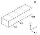
도 3은 본 발명의 실시 예에 따른 메모리 블럭에 포함된 메모리 스트링을 설명하기 위한 입체도이다.
도 4는 도 3에 도시된 메모리 스트링을 설명하기 위한 회로도이다.
도 5는 본 발명의 실시 예에 따른 반도체 메모리 장치의 동작을 설명하기 위한 순서도이다.
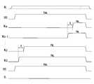
도 6은 본 발명의 실시 예에 따른 반도체 메모리 장치의 동작을 설명하기 위한 동작 전압들의 타이밍도이다.
도 7은 본 발명의 다른 실시 예에 따른 반도체 메모리 장치의 동작을 설명하기 위한 순서도이다.
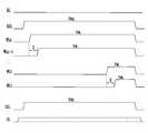
도 8은 본 발명의 다른 실시 예에 따른 반도체 메모리 장치의 동작을 설명하기 위한 동작 전압들의 타이밍도이다.
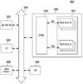
도 9는 도 1의 반도체 메모리 장치를 포함하는 메모리 시스템을 보여주는 블럭도이다.
도 10은 도 9의 메모리 시스템의 응용 예를 보여주는 블럭도이다.
도 11은 도 10을 참조하여 설명된 메모리 시스템을 포함하는 컴퓨팅 시스템을 보여주는 블럭도이다.1 is a block diagram for explaining a semiconductor memory device according to an embodiment of the present invention.
2 is a block diagram showing an embodiment of the memory cell array of FIG.
3 is a perspective view illustrating a memory string included in a memory block according to an embodiment of the present invention.
4 is a circuit diagram for explaining the memory string shown in FIG.
5 is a flowchart illustrating an operation of a semiconductor memory device according to an embodiment of the present invention.
6 is a timing chart of operation voltages for explaining the operation of the semiconductor memory device according to the embodiment of the present invention.
7 is a flowchart illustrating an operation of a semiconductor memory device according to another embodiment of the present invention.
8 is a timing chart of operation voltages for explaining the operation of the semiconductor memory device according to another embodiment of the present invention.
9 is a block diagram showing a memory system including the semiconductor memory device of FIG.
10 is a block diagram showing an application example of the memory system of FIG.
11 is a block diagram illustrating a computing system including the memory system described with reference to FIG.
본 발명의 이점 및 특징, 그리고 그것을 달성하는 방법은 첨부되는 도면과 함께 상세하게 후술되어 있는 실시 예들을 통해 설명될 것이다. 그러나 본 발명은 여기에서 설명되는 실시 예들에 한정되지 않고 다른 형태로 구체화될 수도 있다. 단지, 본 실시 예들은 본 발명이 속하는 기술분야에서 통상의 지식을 가진 자에게 본 발명의 기술적 사상을 용이하게 실시할 수 있을 정도로 상세히 설명하기 위하여 제공되는 것이다.BRIEF DESCRIPTION OF THE DRAWINGS The advantages and features of the present invention, and how to accomplish it, will be described with reference to the embodiments described in detail below with reference to the accompanying drawings. However, the present invention is not limited to the embodiments described herein but may be embodied in other forms. The embodiments are provided so that those skilled in the art can easily carry out the technical idea of the present invention to those skilled in the art.
명세서 전체에서, 어떤 부분이 다른 부분과 "연결"되어 있다고 할 때, 이는 "직접적으로 연결"되어 있는 경우뿐 아니라, 그 중간에 다른 소자를 사이에 두고 "간접적으로 연결"되어 있는 경우도 포함한다. 명세서 전체에서, 어떤 부분이 어떤 구성요소를 "포함"한다고 할 때, 이는 특별히 반대되는 기재가 없는 한 다른 구성요소를 제외하는 것이 아니라 다른 구성요소를 더 포함할 수 있는 것을 의미한다.Throughout the specification, when a part is referred to as being "connected" to another part, it includes not only "directly connected" but also "indirectly connected" . Throughout the specification, when an element is referred to as "comprising ", it means that it can include other elements as well, without excluding other elements unless specifically stated otherwise.
도 1은 본 발명에 따른 반도체 메모리 장치를 설명하기 위한 블럭도이다.1 is a block diagram for explaining a semiconductor memory device according to the present invention.
도 1을 참조하면, 반도체 메모리 장치(100)는 메모리 셀 어레이(110), 어드레스 디코더(120), 읽기 및 쓰기 회로(130), 제어 로직(140), 그리고 전압 생성부(150)를 포함한다.1, a
메모리 셀 어레이(110)는 복수의 메모리 블록들(BLK1~BLKz)을 포함한다. 복수의 메모리 블록들(BLK1~BLKz)은 워드 라인들(WL)을 통해 어드레스 디코더(120)에 연결된다. 복수의 메모리 블록들(BLK1~BLKz)은 비트 라인들(BL1 내지 BLm)을 통해 읽기 및 쓰기 회로(130)에 연결된다. 복수의 메모리 블록들(BLK1~BLKz) 각각은 복수의 메모리 셀들을 포함한다. 실시 예로서, 복수의 메모리 셀들은 불휘발성 메모리 셀들이며, 보다 상세하게 복수의 메모리 셀들은 차지 트랩 디바이스(charge trap device) 기반의 불휘발성 메모리 셀들일 수 있다. 복수의 메모리 셀들은 동일 워드라인에 연결된 메모리 셀들을 하나의 페이지로 정의된다. 즉 메모리 셀 어레이(110)는 다수의 페이지로 구성된다. 또한 메모리 셀 어레이(110)의 복수의 메모리 블록들(BLK1~BLKz) 각각은 다수의 스트링을 포함한다. 다수의 스트링 각각은 비트라인과 소스 라인 사이에 직렬 연결된 드레인 선택 트랜지스터, 다수의 메모리 셀들, 및 소스 선택 트랜지스터를 포함한다.The
어드레스 디코더(120), 읽기 및 쓰기 회로(130), 및 전압 생성부(150)는 메모리 셀 어레이(110)를 구동하는 주변 회로로서 동작한다.The
어드레스 디코더(120)는 워드라인들(WL)을 통해 메모리 셀 어레이(110)에 연결된다. 어드레스 디코더(120)는 제어 로직(140)의 제어에 응답하여 동작하도록 구성된다. 어드레스 디코더(120)는 반도체 메모리 장치(100) 내부의 입출력 버퍼(미도시)를 통해 어드레스(ADDR)를 수신한다.The
어드레스 디코더(120)는 프로그램 전압 인가 동작 시 전압 생성부(150)에서 생성된 드레인 선택 라인 전압(VDSL), 소스 선택 라인 전압(VSSL), 및 디스차지 제어 전압(VWL)을 행 어드레스를 디코딩하고 디코딩된 행 어드레스에 따라 메모리 셀 어레이(110)의 드레인 선택 라인(DSL), 소스 선택 라인(SSL) 및 다수의 워드라인들(WL)에 인가한다.The
어드레스 디코더(120)는 블록 디코더, 행 디코더, 열 디코더 및 어드레스 버퍼 등을 포함할 수 있다.The
읽기 및 쓰기 회로(130)는 복수의 페이지 버퍼들(PB1~PBm)을 포함한다. 복수의 페이지 버퍼들(PB1~PBm)은 비트 라인들(BL1 내지 BLm)을 통해 메모리 셀 어레이(110)에 연결된다. 복수의 페이지 버퍼들(PB1~PBm) 각각은 리드 동작, 프로그램 검증 동작, 소거 검증 동작과 같이 비트라인의 전위 레벨 또는 전류량을 센싱하는 센싱 동작을 수행하기 전에 메모리 스트링들의 채널에 트랩된 전하들을 디트랩하여 디스차지하기 위하여 대응하는 비트 라인들(BL1 내지 BLm)에 양의 전압을 인가할 수 있다.The read and write
또한 복수의 페이지 버퍼들(PB1~PBm) 각각은 프로그램 동작시 입력된 데이터(DATA)를 임시 저장하고 임시 저장된 데이터에 따라 각각 대응하는 비트라인들(BL1 내지 BLm)의 전위를 제어하고, 리드 동작시 대응하는 대응하는 비트라인들(BL1 내지 BLm)의 전위 또는 전류량을 센싱하여 리드 동작을 수행할 수 있다. 읽기 및 쓰기 회로(130)는 제어 로직(140)의 제어에 응답하여 동작한다.Each of the plurality of page buffers PB1 to PBm temporarily stores input data DATA during a program operation and controls potentials of corresponding bit lines BL1 to BLm according to temporarily stored data, It is possible to sense the potential or the amount of current of the corresponding bit lines BL1 to BLm to perform the read operation. The read and
제어 로직(140)은 어드레스 디코더(120), 읽기 및 쓰기 회로(130), 및 전압 생성부(150)에 연결된다. 제어 로직(140)은 반도체 메모리 장치(100)의 입출력 버퍼(미도시)를 통해 커맨드(CMD)를 수신한다. 제어 로직(140)은 커맨드(CMD)에 응답하여 반도체 메모리 장치(100)의 제반 동작을 제어하도록 구성된다.The
제어 로직(140)은 리드 동작, 프로그램 검증 동작, 소거 검증 동작과 같이 비트라인의 전위 레벨 또는 전류량을 센싱하는 센싱 동작을 수행하기 전에 복수의 메모리 블록들(BLK1~BLKz)에 대한 채널 디스차지 동작을 수행하도록 어드레스 디코더(120), 읽기 및 쓰기 회로(130), 및 전압 생성부(150)를 제어할 수 있다. 예를 들어 제어 로직(140)은 리드 동작, 프로그램 동작, 소거 동작에 대응하는 커맨드(CMD)가 입력될 경우, 복수의 메모리 블록들(BLK1~BLKz)에 대한 채널 디스차지 동작을 수행하도록 어드레스 디코더(120), 읽기 및 쓰기 회로(130), 및 전압 생성부(150)를 제어할 수 있다. 이때, 제어 로직(140)은 복수의 메모리 블록들(BLK1~BLKz) 중 선택된 적어도 하나의 메모리 블록에 대하여 채널 디스차지 동작을 수행하거나, 메모리 셀 어레이(100)에 포함된 전체 메모리 블록들(BLK1~BLKz)에 대하여 채널 디스차지 동작을 수행하도록 어드레스 디코더(120), 읽기 및 쓰기 회로(130), 및 전압 생성부(150)를 제어할 수 있다.The
제어 로직(140)은 상술한 채널 디스차지 동작시 소스 라인과 인접한 메모리 셀에서 부터 비트라인과 인접한 메모리 셀 순으로 순차적으로 디스차지 제어 전압(VWL)이 인가되도록 전압 생성부(150) 및 어드레스 디코더(120)를 제어할 수 있다. 다른 실시 예에서 제어 로직(140)은 상술한 채널 디스차지 동작시 비트라인과 인접한 메모리 셀에서 부터 소스 라인과 인접한 메모리 셀 순으로 순차적으로 디스차지 제어 전압(VWL)이 인가되도록 전압 생성부(150) 및 어드레스 디코더(120)를 제어할 수 있다.The
전압 생성부(150)는 채널 디스차지 동작시 제어 로직(140)의 제어에 따라 드레인 선택 라인 전압(VDSL), 소스 선택 라인 전압(VSSL), 및 디스차지 제어 전압(VWL)을 생성하여 어드레스 디코더(120)로 출력하고, 소스 라인 전압(VSL)을 생성하여 상기 메모리 셀 어레이(110)의 소스 라인에 인가한다.The
도 2는 도 1의 메모리 셀 어레이(110)의 일 실시 예를 보여주는 블록도이다.2 is a block diagram illustrating one embodiment of the
도 2를 참조하면, 메모리 셀 어레이(110)는 복수의 메모리 블록들(BLK1~BLKz)을 포함한다. 각 메모리 블록은 3차원 구조를 갖는다. 각 메모리 블록은 기판위에 적층된 복수의 메모리 셀들을 포함한다. 이러한 복수의 메모리 셀들은 +X 방향, +Y 방향 및 +Z 방향을 따라 배열된다. 각 메모리 블록의 구조의 다양한 실시 예는 후술하는 도 3 및 도 7을 참조하여 설명된다.Referring to FIG. 2, the
도 3은 본 발명에 따른 메모리 블럭에 포함된 메모리 스트링을 설명하기 위한 입체도이다. 도 4는 메모리 스트링을 설명하기 위한 회로도이다.3 is a perspective view for explaining a memory string included in a memory block according to the present invention. 4 is a circuit diagram for explaining a memory string.
도 3 및 도 4를 참조하면, 반도체 기판 상에 소스 라인(SL)이 형성된다. 소스 라인(SL) 상에는 수직 채널층(SP)이 형성된다. 수직 채널층(SP)의 상부는 비트 라인(BL)과 연결된다. 수직 채널층(SP)은 폴리실리콘으로 형성될 수 있다. 수직 채널층(SP)의 서로 다른 높이에서 수직 채널층(SP)을 감싸도록 다수의 도전막들(SSL, WL0~WLn, DSL)이 형성된다. 수직 채널층(SP)의 표면에는 전하 저장막을 포함하는 다층막(미도시)이 형성되며, 다층막은 수직 채널층(SP)과 도전막들(SSL, WL0~WLn, DSL) 사이에도 위치한다. 다층막은 산화막, 질화막, 및 산화막이 순차적으로 적층된 ONO 구조로 형성될 수 있다.Referring to FIGS. 3 and 4, a source line SL is formed on a semiconductor substrate. A vertical channel layer SP is formed on the source line SL. The upper part of the vertical channel layer SP is connected to the bit line BL. The vertical channel layer SP may be formed of polysilicon. A plurality of conductive films SSL, WL0 to WLn, and DSL are formed to surround the vertical channel layer SP at different heights of the vertical channel layer SP. A multilayer film (not shown) including a charge storage film is formed on the surface of the vertical channel layer SP and the multilayer film is also located between the vertical channel layer SP and the conductive films SSL, WL0 to WLn, DSL. The multilayer film may be formed of an ONO structure in which an oxide film, a nitride film, and an oxide film are sequentially laminated.
최하부 도전막은 소스 선택 라인(SSL)이 되고, 최상부 도전막은 드레인 선택 라인(DSL)이 된다. 선택 라인들(SSL, DSL) 사이의 도전막들은 워드 라인들(WL0~WLn)이 된다. 다시 말해, 반도체 기판 상에는 도전막들(SSL, WL0~WLn, DSL)이 다층으로 형성되고, 도전막들(SSL, WL0~WLn, DSL)을 관통하는 수직 채널층(SP)이 비트 라인(BL)과 반도체 기판에 형성된 소스 라인(SL) 사이에 수직으로 연결된다.The lowermost conductive film becomes a source selection line (SSL), and the uppermost conductive film becomes a drain selection line (DSL). The conductive films between the selection lines (SSL, DSL) become the word lines WL0 to WLn. In other words, the conductive films SSL, WL0 to WLn and DSL are formed in multiple layers on the semiconductor substrate and the vertical channel layer SP penetrating the conductive films SSL, WL0 to WLn and DSL is connected to the bit lines BL ) And the source line SL formed on the semiconductor substrate.
최상부 도전막(DSL)이 수직 채널층(SP)을 감싸는 부분에서 드레인 선택 트랜지스터(DST)가 형성되고, 최하부 도전막(SSL)이 수직 채널층(SP)을 감싸는 부분에서 소스 선택 트랜지스터(SST)가 형성된다. 중간 도전막들(WL0~WLn)이 수직 채널층(SP)을 감싸는 부분들에서 메모리 셀들(MC0~MCn)이 형성된다.The drain select transistor DST is formed at the portion where the uppermost conductive film DSL surrounds the vertical channel layer SP and the source select transistor SST is formed at the portion where the lowermost conductive film SSL surrounds the vertical channel layer SP. . The memory cells MC0 to MCn are formed at portions where the intermediate conductive layers WL0 to WLn surround the vertical channel layer SP.
상기의 구조에 의해, 메모리 스트링은 소스 라인(SL)과 비트 라인(BL) 사이에 기판과 수직으로 연결되는 소스 선택 트랜지스터(SST), 메모리 셀들(MC0~MCn) 및 드레인 선택 트랜지스터(DST)를 포함한다. 소스 선택 트랜지스터(SST)는 소스 선택 라인(SSL)으로 인가되는 소스 제어 전압에 따라 메모리 셀들(MC0~MCn)을 소스 라인(SL)과 전기적으로 연결시킨다. 드레인 선택 트랜지스터(DST)는 드레인 선택 라인(DSL)으로 인가되는 드레인 제어 전압에 따라 메모리 셀들(MC0~MCn)을 비트 라인(BL)과 전기적으로 연결시킨다.The memory string has a source select transistor SST, memory cells MC0 to MCn, and a drain select transistor DST which are vertically connected to the substrate between the source line SL and the bit line BL . The source select transistor SST electrically connects the memory cells MC0 to MCn to the source line SL in accordance with a source control voltage applied to the source select line SSL. The drain select transistor DST electrically connects the memory cells MC0 to MCn to the bit line BL in accordance with the drain control voltage applied to the drain select line DSL.
상술한 메모리 스트링의 수직 채널층(SP)은 프로그램 동작 및 리드 동작과 같은 제반 동작시 발생한 전자들이 제반 동작 완료 후에도 잔류하여 채널 내에 트랩될 수 있다. 이렇게 트랩된 전자들은 수직 채널층(SP) 내의 전위 레벨에 따라 유동적일 수 있으며, 트랩된 전자들은 새로운 제반 동작 예를 들어 센싱 동작을 포함하는 리드 동작, 프로그램 검증 동작, 소거 검증 동작의 신뢰성을 저하시킬 수 있다.The above-described vertical channel layer SP of the memory string can remain trapped in the channel even after electrons generated during various operations such as a program operation and a read operation remain after completion of all operations. The electrons thus trapped may be flexible depending on the potential level in the vertical channel layer SP, and the trapped electrons may degrade the reliability of the read operation including the sensing operation, the program verification operation, the erase verify operation, .
도 5는 본 발명의 실시 예에 따른 반도체 메모리 장치의 동작을 설명하기 위한 순서도이다.5 is a flowchart illustrating an operation of a semiconductor memory device according to an embodiment of the present invention.
도 6은 본 발명의 실시 예에 따른 반도체 메모리 장치의 동작을 설명하기 위한 동작 전압들의 타이밍도이다.6 is a timing chart of operation voltages for explaining the operation of the semiconductor memory device according to the embodiment of the present invention.
도 1 내지 도 6을 참조하여, 본 발명의 실시 예에 따른 반도체 메모리 장치의 동작 방법을 설명하면 다음과 같다.The operation of the semiconductor memory device according to the embodiment of the present invention will be described with reference to FIGS. 1 to 6. FIG.
1) 리드 명령 입력(S110)1) Read command input (S110)
제어 로직(140)은 반도체 메모리 장치(100)의 입출력 버퍼(미도시)를 통해 리드 명령에 대응하는 커맨드(CMD)를 수신한다. 제어 로직(140)은 리드 명령에 대응하는 커맨드(CMD)에 응답하여 반도체 메모리 장치(100)의 리드 동작을 수행하기 앞서 채널 디스차지 동작을 수행하기 위해 어드레스 디코더(120), 읽기 및 쓰기 회로(130), 및 전압 생성부(150)를 제어하기 위한 제어 신호들을 생성한다.The
2) 디스차지 제어 전압 인가(S120)2) Discharge control voltage application (S120)
전압 생성부(150)는 제어 로직(140)의 제어에 따라 소스 라인 전압(VSL)을 생성하여 소스 라인(SL)에 인가한다. 읽기 및 쓰기 회로(130)의 복수의 페이지 버퍼들(PB1 내지 PBm)는 제어 로직(140)의 제어에 따라 각각 대응하는 비트라인들(BL1 내지 BLm)에 양의 전압을 인가한다. 이때 비트라인들(BL1 내지 BLm)의 전위 레벨은 소스 라인(SL)의 전위 레벨보다 높도록 제어한다. 소스 라인 전압(VSL)은 접지 전압일 수 있다.The
이 후, 전압 생성부(150)는 드레인 선택 라인 전압(VDSL) 및 소스 선택 라인 전압(VSSL)을 생성하고, 어드레스 디코더(120)는 드레인 선택 라인 전압(VDSL) 및 소스 선택 라인 전압(VSSL)을 메모리 셀 어레이(110)의 드레인 선택 라인(DSL) 및 소스 선택 라인(SSL)에 인가하여 드레인 선택 트랜지스터(DST) 및 소스 선택 트랜지스터(SST)를 턴온시킨다.Thereafter, the
이 후, 다수의 워드라인들(WL0 내지 WLn) 중 소스 선택 라인(SSL)과 인접한 워드라인(WL0)에서 부터 드레인 선택 라인(DSL)과 인접한 워드라인(WLn) 방향 순으로 디스차지 제어 전압(VWL)을 순차적으로 인가한다. 즉, 소스 라인(SL)과 인접한 메모리 셀들(MC0)에서부터 비트라인들(BL1 내지 BLm)과 인접한 메모리 셀(MCn) 순으로 디스차지 제어 전압(VWL)을 순차적으로 인가한다. 이때 순차적으로 인가되는 디스차지 제어 전압(VWL)은 인접한 메모리 셀과 일정한 시간 간격(D)을 갖도록 하여 인가될 수 있다.Thereafter, the discharge control voltage (in the order of the drain select line DSL and the adjacent word line WLn) from the word line WL0 adjacent to the source select line SSL among the plurality of word lines WL0 to WLn VWL ) are sequentially applied. That is, the discharge control voltage VWL is sequentially applied from the memory cells MC0 adjacent to the source line SL to the bit lines BL1 through BLm and the adjacent memory cells MCn. At this time, the sequentially applied discharge control voltage (VWL ) may be applied so as to have a predetermined time interval (D) with the adjacent memory cells.
메모리 셀(MCn)에 디스차지 제어 전압(VWL)이 인가되면, 수직 채널층(SP) 중 메모리 셀(MC0)에 대응하는 채널층의 내부에 잔류하는 정공들은 소스 라인(SL)에 인가되는 접지 전압에 의해 소스 라인(SL) 방향으로 이동하고 전자들은 소스 라인(SL)과 반대 방향, 즉 비트라인들(BL1 내지 BLm) 방향으로 이동한다. 일정 시간(D) 이후 메모리 셀(MC1)에 디스차지 제어 전압(VWL)이 인가되면 수직 채널층(SP) 중 메모리 셀(MC1)에 대응하는 채널층의 내부에 잔류하는 정공들은 소스 라인(SL) 방향으로 이동하고, 메모리 셀(MC0)에 대응하는 채널층에서 유입된 전자들 및 메모리 셀(MC1)에 대응하는 채널층에 잔류하던 전자들은 소스 라인(SL)과 반대 방향으로 이동한다.When the discharge control voltage VWL is applied to the memory cell MCn, the holes remaining in the channel layer corresponding to the memory cell MC0 in the vertical channel layer SP are applied to the source line SL The electrons move in the direction of the source line SL by the ground voltage and the electrons move in the direction opposite to the source line SL, that is, in the bit lines BL1 to BLm. When the discharge control voltage VWL is applied to the memory cell MC1 after the predetermined time D, holes remaining in the channel layer corresponding to the memory cell MC1 in the vertical channel layer SP are discharged to the source line SL, and the electrons flowing in the channel layer corresponding to the memory cell MC0 and the electrons remaining in the channel layer corresponding to the memory cell MC1 move in the direction opposite to the source line SL.
상술한 방식으로 수직 채널층(SP) 내에 잔류하던 정공들은 순차적으로 소스 라인(SL) 방향으로 이동하고 수직 채널층(SP) 내에 잔류하던 전자들은 점차 비트라인들(BL1 내지 BLm) 방향으로 이동하게 되어 디스차지된다.The holes remaining in the vertical channel layer SP sequentially move in the direction of the source line SL and the electrons remaining in the vertical channel layer SP gradually move in the direction of the bit lines BL1 to BLm And discharged.
본 발명의 실시 예에서는 비트라인들(BL1 내지 BLm)에 양의 전압을 드레인 선택 라인(DSL) 및 소스 선택 라인(SSL)에 각각 드레인 선택 전압(VDSL) 및 소스 선택 전압(VSSL)이 인가되기 이전에 인가하는 것으로 도시 및 설명하였으나, 디스차지 효율을 극대화시키기 위하여 드레인 선택 라인(DSL)과 인접한 워드라인(WLn)에 디스차지 제어 전압(VWL)이 인가된 후 비트라인들(BL1 내지 BLm)에 양의 전압을 인가할 수 있다.In the embodiment of the present invention, a positive voltage is applied to the bit lines BL1 to BLm and a drain selection voltage VDSL and a source selection voltage VSSL are applied to the drain selection line DSL and the source selection lineSSL , The discharge control voltage VWL is applied to the word line WLn adjacent to the drain select line DSL in order to maximize the discharge efficiency, and then the bit lines BL1 To BLm.
또한 본 발명의 실시 예에서는 다수의 워드라인들(WL0 내지 WLn)을 개별적으로 선택하여 순차적으로 디스차지 제어 전압(VWL)을 인가하는 것을 설명하였으나, 인접한 적어도 두개 이상의 워드라인들을 하나의 그룹으로 그룹핑하는 방식으로 다수의 워드라인들(WL0 내지 WLn)을 다수의 그룹으로 그룹핑하고, 소스 라인(SL)과 인접한 그룹에서부터 비트라인들(BL1 내지 BLm)과 인접한 그룹 순으로 순차적으로 선택하여 디스차지 제어 전압(VWL)을 순차적으로 인가할 수 있다.In the embodiment of the present invention, a plurality of word lines WL0 to WLn are individually selected to sequentially apply the discharge control voltage VWL . However, at least two adjacent word lines may be grouped into one group A plurality of word lines WL0 to WLn are grouped into a plurality of groups in a grouping manner and sequentially selected from a group adjacent to the source line SL to adjacent bit lines BL1 to BLm, The control voltage VWL can be sequentially applied.
상술한 실시 예에서는 소스 라인(SL)에 접지 전압의 전위 레벨을 갖는 소스 라인 전압(VSL)을 계속적으로 인가하는 것으로 설명하였으나, 소스 선택 라인(SSL)에 양의 전위 레벨을 갖는 소스 선택 라인 전압(VSSL)이 인가되기 전에 소스 라인(SL)에 일정 시간 동안 양의 전압을 인가한 후 접지 전압으로 전위 레벨을 하강시킬 수 있다. 이로 인하여 소스 선택 트랜지스터(SST)의 수직 채널층에 잔류하는 전자들을 소스 라인(SL) 방향으로 집중 시킬 수 있다.Although the source line voltage VSL having the potential level of the ground voltage is continuously applied to the source line SL in the above-described embodiment, the source line voltage VSL having the positive potential level The potential level may be lowered to the ground voltage after a positive voltage is applied to the source line SL for a predetermined time before the voltage VSSL is applied. This makes it possible to concentrate the electrons remaining in the vertical channel layer of the source selection transistor SST in the direction of the source line SL.
3) 리드 동작 수행(S130)3) Performing the read operation (S130)
상술한 S120 단계에 의해 채널 디스차지 동작이 완료된 후, 제어 로직(140)은 주변 회로들을 제어하여 반도체 메모리 장치의 리드 동작을 수행한다.After the channel discharge operation is completed in step S120, the
상술한 바와 같이 본원 발명의 일 실시 예에 따르면, 리드 명령이 입력될 경우 리드 동작을 수행하기 이전에 메모리 스트링의 채널들에 잔류하는 전자 및 정공들을 디스차지하여 후속 수행되는 리드 동작의 신뢰성을 개선할 수 있다.As described above, according to an embodiment of the present invention, when a read command is input, electrons and holes remaining in the channels of the memory string are discharged before performing the read operation, thereby improving the reliability of the subsequent read operation can do.
도 7은 본 발명의 다른 실시 예에 따른 반도체 메모리 장치의 동작을 설명하기 위한 순서도이다.7 is a flowchart illustrating an operation of a semiconductor memory device according to another embodiment of the present invention.
도 8은 본 발명의 다른 실시 예에 따른 반도체 메모리 장치의 동작을 설명하기 위한 동작 전압들의 타이밍도이다.8 is a timing chart of operation voltages for explaining the operation of the semiconductor memory device according to another embodiment of the present invention.
도 1 내지 도 4, 도 7 및 도 8을 참조하여, 본 발명의 다른 실시 예에 따른 반도체 메모리 장치의 동작 방법을 설명하면 다음과 같다.A method of operating the semiconductor memory device according to another embodiment of the present invention will be described with reference to FIGS. 1 to 4, 7, and 8. FIG.
1) 리드 명령 입력(S210)1) Read command input (S210)
제어 로직(140)은 반도체 메모리 장치(100)의 입출력 버퍼(미도시)를 통해 리드 명령에 대응하는 커맨드(CMD)를 수신한다. 제어 로직(140)은 리드 명령에 대응하는 커맨드(CMD)에 응답하여 반도체 메모리 장치(100)의 리드 동작을 수행하기 앞서 채널 디스차지 동작을 수행하기 위해 어드레스 디코더(120), 읽기 및 쓰기 회로(130), 및 전압 생성부(150)를 제어하기 위한 제어 신호들을 생성한다.The
2) 디스차지 제어 전압 인가(S220)2) Discharge control voltage application (S220)
읽기 및 쓰기 회로(130)의 복수의 페이지 버퍼들(PB1 내지 PBm)는 제어 로직(140)의 제어에 따라 각각 대응하는 비트라인들(BL1 내지 BLm)에 접지 전압을 인가한다. 전압 생성부(150)는 제어 로직(140)의 제어에 따라 소스 라인 전압(VSL)을 생성하여 소스 라인(SL)에 인가한다. 이때 소스 라인 전압(VSL)은 비트라인들(BL1 내지 BLm)에 인가하는 전압보다 높다. 소스 라인 전압(VSL)은 양의 전위 레벨을 갖는다.The plurality of page buffers PB1 to PBm of the read and write
이 후, 전압 생성부(150)는 드레인 선택 라인 전압(VDSL) 및 소스 선택 라인 전압(VSSL)을 생성하고, 어드레스 디코더(120)는 드레인 선택 라인 전압(VDSL) 및 소스 선택 라인 전압(VSSL)을 메모리 셀 어레이(110)의 드레인 선택 라인(DSL) 및 소스 선택 라인(SSL)에 인가하여 드레인 선택 트랜지스터(DST) 및 소스 선택 트랜지스터(SST)를 턴온시킨다.Thereafter, the
이 후, 다수의 워드라인들(WL0 내지 WLn) 중 드레인 선택 라인(DSL)과 인접한 워드라인(WLn)에서 부터 소스 선택 라인(SSL)과 인접한 워드라인(WL0) 방향 순으로 디스차지 제어 전압(VWL)을 순차적으로 인가한다. 즉, 비트라인들(BL1 내지 BLm)과 인접한 메모리 셀(MCn)에서부터 소스 라인(SL)과 인접한 메모리 셀(MC0) 순으로 디스차지 제어 전압(VWL)을 순차적으로 인가한다. 이때 순차적으로 인가되는 디스차지 제어 전압(VWL)은 인접한 메모리 셀과 일정한 시간 간격(D)을 갖도록 하여 인가될 수 있다.Thereafter, the discharge control voltage (in the order of the source select line SSL and the adjacent word line WL0 from the word line WLn adjacent to the drain select line DSL of the plurality of word lines WL0 to WLn) VWL ) are sequentially applied. That is, the discharge control voltage VWL is sequentially applied from the memory cells MCn adjacent to the bit lines BL1 to BLm to the source line SL and the memory cell MC0 adjacent thereto. At this time, the sequentially applied discharge control voltage (VWL ) may be applied so as to have a predetermined time interval (D) with the adjacent memory cells.
메모리 셀(MCn)에 디스차지 제어 전압(VWL)이 인가되면, 수직 채널층(SP) 중 메모리 셀(MCn)에 대응하는 채널층의 내부에 잔류하는 정공들은 비트라인들(BL1 내지 BLm)에 인가되는 접지 전압에 의해 비트라인들(BL1 내지 BLm) 방향으로 이동하고 전자들은 비트라인들(BL1 내지 BLm)과 반대 방향, 즉 소스 라인(SL) 방향으로 이동한다. 일정 시간(D) 이후 메모리 셀(MCn-1)에 디스차지 제어 전압(VWL)이 인가되면 수직 채널층(SP) 중 메모리 셀(MCn-1)에 대응하는 채널층의 내부에 잔류하는 정공들은 비트라인들(BL1 내지 BLm) 방향으로 이동하고, 메모리 셀(MCn)에 대응하는 채널층에서 유입된 전자들 및 메모리 셀(MCn-1)에 대응하는 채널층에 잔류하던 전자들은 비트라인들(BL1 내지 BLm)과 반대 방향으로 이동한다.When the discharge control voltage VWL is applied to the memory cell MCn, the holes remaining in the channel layer corresponding to the memory cell MCn among the vertical channel layer SP are connected to the bit lines BL1 to BLm, And the electrons move in the direction opposite to the bit lines BL1 to BLm, that is, in the direction of the source line SL. When a discharge control voltage VWL is applied to the memory cell MCn-1 after the predetermined time D, the remaining holes in the channel layer corresponding to the memory cell MCn-1 in the vertical channel layer SP The electrons flowing in the channel layer corresponding to the memory cell MCn and the electrons remaining in the channel layer corresponding to the memory cell MCn-1 move in the direction of the bit lines BL1 to BLm, (BL1 to BLm).
상술한 방식으로 수직 채널층(SP) 내에 잔류하던 정공들은 순차적으로 비트라인들(BL1 내지 BLm) 방향으로 이동하고 수직 채널층(SP) 내에 잔류하던 전자들은 점차 소스 라인(SL) 방향으로 이동하게 되어 디스차지된다.The holes remaining in the vertical channel layer SP sequentially move in the direction of the bit lines BL1 to BLm and the electrons remaining in the vertical channel layer SP gradually move toward the source line SL And discharged.
본 발명의 실시 예에서는 소스 라인(SL)에 양의 전압을 드레인 선택 라인(DSL) 및 소스 선택 라인(SSL) 각각에 드레인 선택 전압(VDSL) 및 소스 선택 전압(VSSL)이 인가되기 이전에 인가하는 것으로 도시 및 설명하였으나, 디스차지 효율을 극대화시키기 위하여 소스 선택 라인(SSL)과 인접한 워드라인(WL0)에 디스차지 제어 전압(VWL)이 인가된 후 소스 라인(SL)에 양의 전압을 인가할 수 있다.In the embodiment of the present invention, a positive voltage is applied to the source line SL before the drain selection voltage VDSL and the source selection voltage VSSL are applied to the drain selection line DSL and the source selection line SSL, The discharge control voltage VWL is applied to the word line WL0 adjacent to the source select line SSL to maximize the discharge efficiency and then the source line SL is applied with a positive Voltage can be applied.
또한 본 발명의 실시 예에서는 다수의 워드라인들(WL0 내지 WLn)을 개별적으로 선택하여 순차적으로 디스차지 제어 전압(VWL)을 인가하는 것을 설명하였으나, 인접한 적어도 두개 이상의 워드라인들을 하나의 그룹으로 그룹핑하는 방식으로 다수의 워드라인들(WL0 내지 WLn)을 다수의 그룹으로 그룹핑하고, 비트라인들(BL1 내지 BLm)과 인접한 그룹에서부터 소스 라인(SL)과 인접한 그룹 순으로 순차적으로 선택하여 디스차지 제어 전압(VWL)을 순차적으로 인가할 수 있다.In the embodiment of the present invention, a plurality of word lines WL0 to WLn are individually selected to sequentially apply the discharge control voltage VWL . However, at least two adjacent word lines may be grouped into one group A plurality of word lines WL0 to WLn are grouped into a plurality of groups in a grouping manner and sequentially selected from a group adjacent to the bit lines BL1 to BLm and a group adjacent to the source line SL, The control voltage VWL can be sequentially applied.
3) 리드 동작 수행(S230)3) Performing the read operation (S230)
상술한 S220 단계에 의해 채널 디스차지 동작이 완료된 후, 제어 로직(140)은 주변 회로들을 제어하여 반도체 메모리 장치의 리드 동작을 수행한다.After the channel discharge operation is completed by the above-described step S220, the
상술한 바와 같이 본원 발명의 일 실시 예에 따르면, 리드 명령이 입력될 경우 리드 동작을 수행하기 이전에 메모리 스트링의 채널들에 잔류하는 전자 및 정공들을 디스차지하여 후속 수행되는 리드 동작의 신뢰성을 개선할 수 있다.As described above, according to an embodiment of the present invention, when a read command is input, electrons and holes remaining in the channels of the memory string are discharged before performing the read operation, thereby improving the reliability of the subsequent read operation can do.
본 발명의 일 실시 예 및 다른 실시 예에서는 리드 동작에 대한 커맨드가 입력될 경우를 일 예로 설명하였으나, 센싱 동작을 수행하는 프로그램 검증 동작, 소거 검증 동작도 유사한 방식으로 수행될 수 있다. 즉 프로그램 동작에 대한 커맨드 또는 소거 동작에 대한 커맨드가 입력될 경우 프로그램 동작 또는 소거 동작을 수행하기 이전에 채널 디스차지 동작을 수행할 수 있다.In one embodiment and another embodiment of the present invention, a case where a command for a read operation is input is described as an example, but a program verify operation and an erase verify operation for performing a sensing operation may be performed in a similar manner. That is, when a command for a program operation or a command for an erase operation is inputted, the channel discharge operation can be performed before performing the program operation or the erase operation.
본 발명의 일 실시 예 및 다른 실시 예에서는 반도체 메모리 장치의 제반 동작(리드 동작, 센싱 동작을 수행하는 프로그램 검증 및 소거 검증 동작)을 수행하기 이전에 디스차지 제어 전압을 인가하여 채널 디스차지 동작을 수행하는 것으로 기재하였으나, 반도체 메모리 장치의 제반 동작 예를 들어 리드 동작, 프로그램 동작, 소거 동작 등을 수행한 후 채널 디스차지 동작을 수행할 수 있다. 이로 인하여 제반 동작시 워드라인에 인가된 전압에 따라 채널에 잔류하는 전자들을 채널 디스차지 동작으로 디스차지시킬 수 있다.In one embodiment and another embodiment of the present invention, the discharge control voltage is applied to perform the channel discharge operation before performing all the operations of the semiconductor memory device (the read operation, the program verify and the erase verify operation for performing the sensing operation) However, it is possible to perform a channel discharge operation after performing all operations of the semiconductor memory device, for example, a read operation, a program operation, an erase operation, and the like. Accordingly, electrons remaining in the channel can be discharged by the channel discharge operation according to the voltage applied to the word line during the entire operation.
도 9를 참조하면, 메모리 시스템(1000)은 반도체 메모리 장치(100) 및 컨트롤러(1100)를 포함한다.9, a
반도체 메모리 장치(100)는 도 1을 참조하여 설명된 바와 마찬가지로 구성되고, 동작할 수 있다. 이하, 중복되는 설명은 생략된다.The
컨트롤러(1100)는 호스트(Host) 및 반도체 메모리 장치(100)에 연결된다. 호스트(Host)로부터의 요청에 응답하여, 컨트롤러(1100)는 반도체 메모리 장치(100)를 액세스하도록 구성된다. 예를 들면, 컨트롤러(1100)는 반도체 메모리 장치(100)의 읽기, 쓰기, 소거, 그리고 배경(background) 동작을 제어하도록 구성된다. 컨트롤러(1100)는 반도체 메모리 장치(100) 및 호스트(Host) 사이에 인터페이스를 제공하도록 구성된다. 컨트롤러(1100)는 반도체 메모리 장치(100)를 제어하기 위한 펌웨어(firmware)를 구동하도록 구성된다.The
컨트롤러(1100)는 램(1110, Random Access Memory), 프로세싱 유닛(1120, processing unit), 호스트 인터페이스(1130, host interface), 메모리 인터페이스(1140, memory interface) 및 에러 정정 블록(1150)을 포함한다. 램(1110)은 프로세싱 유닛(1120)의 동작 메모리, 반도체 메모리 장치(100) 및 호스트(Host) 사이의 캐시 메모리, 그리고 반도체 메모리 장치(100) 및 호스트(Host) 사이의 버퍼 메모리 중 적어도 하나로서 이용된다. 프로세싱 유닛(1120)은 컨트롤러(1100)의 제반 동작을 제어한다. 또한 컨트롤러(1100)는 쓰기 동작시 호스트(Host)로 부터 제공되는 프로그램 데이터를 임시 저장할 수 있다.The
호스트 인터페이스(1130)는 호스트(Host) 및 컨트롤러(1100) 사이의 데이터 교환을 수행하기 위한 프로토콜을 포함한다. 예시적인 실시 예로서, 컨트롤러(1200)는 USB (Universal Serial Bus) 프로토콜, MMC (multimedia card) 프로토콜, PCI (peripheral component interconnection) 프로토콜, PCI-E (PCI-express) 프로토콜, ATA (Advanced Technology Attachment) 프로토콜, Serial-ATA 프로토콜, Parallel-ATA 프로토콜, SCSI (small computer small interface) 프로토콜, ESDI (enhanced small disk interface) 프로토콜, 그리고 IDE (Integrated Drive Electronics) 프로토콜, 사유(private) 프로토콜 등과 같은 다양한 인터페이스 프로토콜들 중 적어도 하나를 통해 호스트(Host)와 통신하도록 구성된다.The
메모리 인터페이스(1140)는 반도체 메모리 장치(100)와 인터페이싱한다. 예를 들면, 메모리 인터페이스는 낸드 인터페이스 또는 노어 인터페이스를 포함한다.The
에러 정정 블록(1150)은 에러 정정 코드(ECC, Error Correcting Code)를 이용하여 반도체 메모리 장치(100)로부터 수신된 데이터의 에러를 검출하고, 정정하도록 구성된다. 프로세싱 유닛(1120)은 에러 정정 블록(1150)의 에러 검출 결과에 따라 읽기 전압을 조절하고, 재 읽기를 수행하도록 반도체 메모리 장치(100)를 제어할 것이다. 예시적인 실시 예로서, 에러 정정 블록은 컨트롤러(1100)의 구성 요소로서 제공될 수 있다.The
컨트롤러(1100) 및 반도체 메모리 장치(100)는 하나의 반도체 장치로 집적될 수 있다. 예시적인 실시 예로서, 컨트롤러(1100) 및 반도체 메모리 장치(100)는 하나의 반도체 장치로 집적되어, 메모리 카드를 구성할 수 있다. 예를 들면, 컨트롤러(1100) 및 반도체 메모리 장치(100)는 하나의 반도체 장치로 집적되어 PC 카드(PCMCIA, personal computer memory card international association), 컴팩트 플래시 카드(CF), 스마트 미디어 카드(SM, SMC), 메모리 스틱, 멀티미디어 카드(MMC, RS-MMC, MMCmicro), SD 카드(SD, miniSD, microSD, SDHC), 유니버설 플래시 기억장치(UFS) 등과 같은 메모리 카드를 구성할 것이다.The
컨트롤러(1100) 및 반도체 메모리 장치(100)는 하나의 반도체 장치로 집적되어 반도체 드라이브(SSD, Solid State Drive)를 구성할 수 있다. 반도체 드라이브(SSD)는 반도체 메모리에 데이터를 저장하도록 구성되는 저장 장치를 포함한다. 메모리 시스템(1000)이 반도체 드라이브(SSD)로 이용되는 경우, 메모리 시스템(2000)에 연결된 호스트(Host)의 동작 속도는 획기적으로 개선된다.The
다른 예로서, 메모리 시스템(1000)은 컴퓨터, UMPC (Ultra Mobile PC), 워크스테이션, 넷북(net-book), PDA (Personal Digital Assistants), 포터블(portable) 컴퓨터, 웹 타블렛(web tablet), 무선 전화기(wireless phone), 모바일 폰(mobile phone), 스마트폰(smart phone), e-북(e-book), PMP(portable multimedia player), 휴대용 게임기, 네비게이션(navigation) 장치, 블랙박스(black box), 디지털 카메라(digital camera), 3차원 수상기(3-dimensional television), 디지털 음성 녹음기(digital audio recorder), 디지털 음성 재생기(digital audio player), 디지털 영상 녹화기(digital picture recorder), 디지털 영상 재생기(digital picture player), 디지털 동영상 녹화기(digital video recorder), 디지털 동영상 재생기(digital video player), 정보를 무선 환경에서 송수신할 수 있는 장치, 홈 네트워크를 구성하는 다양한 전자 장치들 중 하나, 컴퓨터 네트워크를 구성하는 다양한 전자 장치들 중 하나, 텔레매틱스 네트워크를 구성하는 다양한 전자 장치들 중 하나, RFID 장치, 또는 컴퓨팅 시스템을 구성하는 다양한 구성 요소들 중 하나 등과 같은 전자 장치의 다양한 구성 요소들 중 하나로 제공된다.As another example, the
예시적인 실시 예로서, 반도체 메모리 장치(100) 또는 메모리 시스템(1000)은 다양한 형태들의 패키지로 실장될 수 있다. 예를 들면, 반도체 메모리 장치(100) 또는 메모리 시스템(1000)은 PoP(Package on Package), Ball grid arrays(BGAs), Chip scale packages(CSPs), Plastic Leaded Chip Carrier(PLCC), Plastic Dual In Line Package(PDIP), Die in Waffle Pack, Die in Wafer Form, Chip On Board(COB), Ceramic Dual In Line Package(CERDIP), Plastic Metric Quad Flat Pack(MQFP), Thin Quad Flatpack(TQFP), Small Outline(SOIC), Shrink Small Outline Package(SSOP), Thin Small Outline(TSOP), Thin Quad Flatpack(TQFP), System In Package(SIP), Multi Chip Package(MCP), Wafer-level Fabricated Package(WFP), Wafer-Level Processed Stack Package(WSP) 등과 같은 방식으로 패키지화되어 실장될 수 있다.As an exemplary embodiment,
도 10은 도 9의 메모리 시스템의 응용 예를 보여주는 블럭도이다.10 is a block diagram showing an application example of the memory system of FIG.
도 10을 참조하면, 메모리 시스템(2000)은 반도체 메모리 장치(2100) 및 컨트롤러(2200)를 포함한다. 반도체 메모리 장치(2100)는 복수의 반도체 메모리 칩들을 포함한다. 복수의 반도체 메모리 칩들은 복수의 그룹들로 분할된다.10, the
도 10에서, 복수의 그룹들은 각각 제 1 내지 제 k 채널들(CH1~CHk)을 통해 컨트롤러(2200)와 통신하는 것으로 도시되어 있다. 각 반도체 메모리 칩은 도 1을 참조하여 설명된 반도체 메모리 장치(100) 중 하나와 마찬가지로 구성되고, 동작할 것이다.In Fig. 10, a plurality of groups are shown communicating with the
각 그룹은 하나의 공통 채널을 통해 컨트롤러(2200)와 통신하도록 구성된다. 컨트롤러(2200)는 도 9를 참조하여 설명된 컨트롤러(1100)와 마찬가지로 구성되고, 복수의 채널들(CH1~CHk)을 통해 반도체 메모리 장치(2100)의 복수의 메모리 칩들을 제어하도록 구성된다.Each group is configured to communicate with the
도 11은 도 10을 참조하여 설명된 메모리 시스템을 포함하는 컴퓨팅 시스템을 보여주는 블럭도이다.11 is a block diagram illustrating a computing system including the memory system described with reference to FIG.
도 11을 참조하면, 컴퓨팅 시스템(3000)은 중앙 처리 장치(3100), 램(3200, RAM, Random Access Memory), 사용자 인터페이스(3300), 전원(3400), 시스템 버스(3500), 그리고 메모리 시스템(2000)을 포함한다.11, a
메모리 시스템(2000)은 시스템 버스(3500)를 통해, 중앙처리장치(3100), 램(3200), 사용자 인터페이스(3300), 그리고 전원(3400)에 전기적으로 연결된다. 사용자 인터페이스(3300)를 통해 제공되거나, 중앙 처리 장치(3100)에 의해서 처리된 데이터는 메모리 시스템(2000)에 저장된다.The
도 11에서, 반도체 메모리 장치(2100)는 컨트롤러(2200)를 통해 시스템 버스(3500)에 연결되는 것으로 도시되어 있다. 그러나, 반도체 메모리 장치(2100)는 시스템 버스(3500)에 직접 연결되도록 구성될 수 있다. 이때, 컨트롤러(2200)의 기능은 중앙 처리 장치(3100) 및 램(3200)에 의해 수행될 것이다.11, the
도 11에서, 도 10을 참조하여 설명된 메모리 시스템(2000)이 제공되는 것으로 도시되어 있다. 그러나, 메모리 시스템(2000)은 도 9를 참조하여 설명된 메모리 시스템(1000)으로 대체될 수 있다. 예시적인 실시 예로서, 컴퓨팅 시스템(3000)은 도 9 및 도 10을 참조하여 설명된 메모리 시스템들(1000, 2000)을 모두 포함하도록 구성될 수 있다.In Fig. 11, it is shown that the
본 발명의 상세한 설명에서는 구체적인 실시 예에 관하여 설명하였으나, 본 발명의 범위와 기술적 사상에서 벗어나지 않는 한도 내에서 다양한 변경이 가능하다. 그러므로 본 발명의 범위는 상술한 실시 예에 국한되어 정해져서는 안되며 후술하는 특허청구범위뿐만 아니라 이 발명의 특허청구범위와 균등한 것들에 의해 정해져야 한다.While the invention has been shown and described with reference to certain preferred embodiments thereof, it will be understood by those skilled in the art that various changes and modifications may be made without departing from the spirit and scope of the invention. Therefore, the scope of the present invention should not be limited to the above-described embodiments, but should be determined by the equivalents of the claims of the present invention as well as the claims of the following.
100: 반도체 메모리 장치
110: 메모리 셀 어레이
120: 어드레스 디코더
130: 읽기 및 쓰기 회로
140: 제어 로직
150 : 전압 생성부100: semiconductor memory device
110: memory cell array
120: address decoder
130: Read and Write Circuit
140: control logic
150:
Claims (20)
Translated fromKorean소스 라인에 연결된 소스 선택 트랜지스터;
상기 드레인 선택 트랜지스터와 상기 소스 선택 트랜지스터 사이에 직렬 연결된 복수의 메모리 셀들; 및
상기 소스 선택 트랜지스터와 인접한 메모리 셀부터 상기 드레인 선택 트랜지스터와 인접한 메모리 셀까지 순차적으로 디스차지 제어 전압을 인가하기 위한 주변 회로를 포함하는 반도체 메모리 장치.
A drain select transistor connected to the bit line;
A source select transistor coupled to a source line;
A plurality of memory cells serially connected between the drain select transistor and the source select transistor; And
And a peripheral circuit for sequentially applying a discharge control voltage from a memory cell adjacent to the source selection transistor to a memory cell adjacent to the drain selection transistor.
상기 주변 회로는 상기 비트라인에 제1 전압을 인가하고, 상기 소스 라인에 제1 전압보다 낮은 제2 전압을 인가하는 반도체 메모리 장치.
The method according to claim 1,
The peripheral circuit applies a first voltage to the bit line and applies a second voltage lower than the first voltage to the source line.
상기 제1 전압은 양의 전위를 갖는 전압이며, 상기 제2 전압은 접지 전압인 반도체 메모리 장치.
3. The method of claim 2,
Wherein the first voltage is a voltage having a positive potential and the second voltage is a ground voltage.
상기 주변 회로는 상기 복수의 메모리 셀들에 상기 디스차지 제어 전압을 인가하기 이전에,
상기 비트라인 및 상기 소스 라인에 상기 제1 및 제2 전압을 인가하고 상기 드레인 선택 트랜지스터 및 상기 소스 선택 트랜지스터에 드레인 선택 라인 전압 및 소스 선택 라인 전압을 인가하기 위한 반도체 메모리 장치.
3. The method of claim 2,
Wherein the peripheral circuit is configured to, prior to applying the discharge control voltage to the plurality of memory cells,
To apply the first and second voltages to the bit line and the source line, and to apply a drain select line voltage and a source select line voltage to the drain select transistor and the source select transistor.
상기 주변 회로는 상기 복수의 메모리 셀들 중 상기 드레인 선택 트랜지스터와 인접한 메모리 셀에 상기 디스차지 제어 전압을 인가한 후, 상기 비트라인에 상기 제1 전압을 인가하는 반도체 메모리 장치.
3. The method of claim 2,
The peripheral circuit applies the discharge control voltage to the memory cell adjacent to the drain selection transistor among the plurality of memory cells, and then applies the first voltage to the bit line.
상기 주변 회로는 상기 복수의 메모리 셀들을 다수의 메모리 그룹으로 구분하고, 상기 소스 라인과 인접한 메모리 그룹에서부터 상기 비트 라인과 인접한 메모리 그룹에 순차적으로 상기 디스차지 제어 전압을 인가하는 반도체 메모리 장치.
3. The method of claim 2,
Wherein the peripheral circuit divides the plurality of memory cells into a plurality of memory groups and sequentially applies the discharge control voltage from a memory group adjacent to the source line to a memory group adjacent to the bit line.
상기 주변 회로는 센싱 동작을 수행하기 이전 또는 제반 동작 수행 이후에 상기 디스차지 제어 전압을 인가하는 반도체 메모리 장치.
The method according to claim 1,
Wherein the peripheral circuit applies the discharge control voltage before performing the sensing operation or after performing the overall operation.
상기 메모리 셀 어레이에 동작 전압들을 인가하기 위한 주변 회로; 및
상기 다수의 메모리 스트링들과 연결된 다수의 워드라인들에 순차적으로 디스차지 제어 전압을 인가하도록 상기 주변 회로를 제어하기 위한 제어 로직을 포함하는 반도체 메모리 장치.
A memory cell array including a plurality of memory strings;
A peripheral circuit for applying operating voltages to the memory cell array; And
And control logic for controlling the peripheral circuit to sequentially apply a discharge control voltage to a plurality of word lines connected to the plurality of memory strings.
상기 주변 회로는 상기 다수의 워드라인들 중 소스 선택 라인과 인접한 워드라인부터 드레인 선택 라인과 인접한 워드라인까지 순차적으로 상기 디스차지 제어 전압을 인가하는 반도체 메모리 장치.
9. The method of claim 8,
Wherein the peripheral circuit sequentially applies the discharge control voltage from a word line adjacent to a source select line to a drain select line and an adjacent word line among the plurality of word lines.
상기 주변 회로는 상기 다수의 메모리 스트링들이 각각 연결된 다수의 비트라인들에는 제1 전압을 인가하고, 상기 다수의 메모리 스트링들이 공통으로 연결된 소스 라인에는 제2 전압을 인가하는 반도체 메모리 장치.
10. The method of claim 9,
Wherein the peripheral circuit applies a first voltage to a plurality of bit lines to which the plurality of memory strings are respectively connected and applies a second voltage to a source line to which the plurality of memory strings are connected in common.
상기 제1 전압은 양의 전위를 갖는 전압이며, 상기 제2 전압은 접지 전압인 반도체 메모리 장치.
11. The method of claim 10,
Wherein the first voltage is a voltage having a positive potential and the second voltage is a ground voltage.
상기 주변 회로는 상기 복수의 워드라인들 상기 디스차지 제어 전압을 인가하기 이전에,
상기 다수의 비트라인들 및 상기 소스 라인에 상기 제1 및 제2 전압을 인가하고 상기 드레인 선택 라인 및 상기 소스 선택 라인에 드레인 선택 라인 전압 및 소스 선택 라인 전압을 인가하는 반도체 메모리 장치.
12. The method of claim 11,
Wherein the peripheral circuit includes a plurality of word lines,
And applies the first and second voltages to the plurality of bit lines and the source line and applies a drain select line voltage and a source select line voltage to the drain select line and the source select line.
상기 주변 회로는 상기 복수의 워드라인들 중 상기 드레인 선택 라인과 인접한 워드라인에 상기 디스차지 제어 전압을 인가한 후, 상기 다수의 비트라인들에 상기 제1 전압을 인가하는 반도체 메모리 장치.
12. The method of claim 11,
Wherein the peripheral circuit applies the discharge control voltage to a word line adjacent to the drain select line among the plurality of word lines and then applies the first voltage to the plurality of bit lines.
상기 주변 회로는 상기 다수의 워드라인들 중 드레인 선택 라인과 인접한 워드라인부터 소스 선택 라인과 인접한 워드라인까지 순차적으로 상기 디스차지 제어 전압을 인가하는 반도체 메모리 장치.
9. The method of claim 8,
Wherein the peripheral circuit sequentially applies the discharge control voltage from a word line adjacent to a drain select line of the plurality of word lines to a word line adjacent to the source select line.
상기 주변 회로는 상기 다수의 메모리 스트링들이 각각 연결된 다수의 비트라인들에는 접지 전압을 인가하고, 상기 다수의 메모리 스트링들이 공통으로 연결된 소스 라인에는 양의 전압을 인가하는 반도체 메모리 장치.
15. The method of claim 14,
Wherein the peripheral circuit applies a ground voltage to a plurality of bit lines to which the plurality of memory strings are connected and applies a positive voltage to a source line to which the plurality of memory strings are commonly connected.
상기 주변 회로는 상기 복수의 워드라인들 상기 디스차지 제어 전압을 인가하기 이전에,
상기 다수의 비트라인들 및 상기 소스 라인에 상기 접지 전압 및 상기 양의 전압 인가하고 상기 드레인 선택 라인 및 상기 소스 선택 라인에 드레인 선택 라인 전압 및 소스 선택 라인 전압을 인가하는 반도체 메모리 장치.
16. The method of claim 15,
Wherein the peripheral circuit includes a plurality of word lines,
And applies the ground voltage and the positive voltage to the plurality of bit lines and the source line and applies a drain select line voltage and a source select line voltage to the drain select line and the source select line.
상기 주변 회로는 상기 복수의 메모리 셀들 중 상기 소스 선택 트랜지스터와 인접한 메모리 셀에 상기 디스차지 제어 전압을 인가한 후, 상기 소스 라인에 상기 양의 전압을 인가하는 반도체 메모리 장치.
16. The method of claim 15,
Wherein the peripheral circuit applies the discharge control voltage to the memory cell adjacent to the source selection transistor among the plurality of memory cells and then applies the positive voltage to the source line.
상기 주변 회로는 상기 다수의 워드라인들을 인접한 적어도 두 개 이상의 워드라인들을 하나의 그룹으로 구분하고, 각 그룹에 상기 디스차지 제어 전압을 순차적으로 인가하는 반도체 메모리 장치.
9. The method of claim 8,
Wherein the peripheral circuit divides the plurality of word lines into at least two adjacent word lines, and sequentially applies the discharge control voltage to each group.
상기 비트라인에 양의 전압을 인가하고, 상기 소스 라인에 접지 전압을 인가하는 단계; 및
상기 소스 라인과 인접한 메모리 셀부터 상기 비트라인과 인접한 메모리 셀 순으로 상기 디스차지 제어 전압을 인가하는 단계를 포함하는 반도체 메모리 장치의 동작 방법.
Providing a plurality of memory cells serially connected between a bit line and a source line;
Applying a positive voltage to the bit line and applying a ground voltage to the source line; And
And applying the discharge control voltage in order from the memory cell adjacent to the source line to the memory cell adjacent to the bit line.
상기 비트라인과 인접한 메모리 셀에 상기 디스차지 제어 전압이 인가된 후, 상기 비트라인에 상기 양의 전압을 인가하는 반도체 메모리 장치의 동작 방법.20. The method of claim 19,
Wherein the positive voltage is applied to the bit line after the discharge control voltage is applied to the memory cell adjacent to the bit line.
Priority Applications (2)
| Application Number | Priority Date | Filing Date | Title |
|---|---|---|---|
| KR1020160002691AKR20170083346A (en) | 2016-01-08 | 2016-01-08 | Semiconductor memory device and operating method thereof |
| US15/173,874US9704587B1 (en) | 2016-01-08 | 2016-06-06 | Semiconductor memory device and operating method thereof |
Applications Claiming Priority (1)
| Application Number | Priority Date | Filing Date | Title |
|---|---|---|---|
| KR1020160002691AKR20170083346A (en) | 2016-01-08 | 2016-01-08 | Semiconductor memory device and operating method thereof |
Publications (1)
| Publication Number | Publication Date |
|---|---|
| KR20170083346Atrue KR20170083346A (en) | 2017-07-18 |
Family
ID=59257244
Family Applications (1)
| Application Number | Title | Priority Date | Filing Date |
|---|---|---|---|
| KR1020160002691ACeasedKR20170083346A (en) | 2016-01-08 | 2016-01-08 | Semiconductor memory device and operating method thereof |
Country Status (2)
| Country | Link |
|---|---|
| US (1) | US9704587B1 (en) |
| KR (1) | KR20170083346A (en) |
Families Citing this family (8)
| Publication number | Priority date | Publication date | Assignee | Title |
|---|---|---|---|---|
| US10115464B1 (en)* | 2017-07-27 | 2018-10-30 | Sandisk Technologies Llc | Electric field to reduce select gate threshold voltage shift |
| CN109411001B (en)* | 2017-08-15 | 2021-07-06 | 华邦电子股份有限公司 | Flash memory storage device and reading method thereof |
| KR102531995B1 (en)* | 2018-03-29 | 2023-05-15 | 에스케이하이닉스 주식회사 | Semiconductor memory device, storage device having the same, and method for operating memory controller |
| KR102736207B1 (en)* | 2018-11-23 | 2024-12-02 | 에스케이하이닉스 주식회사 | Memory device and operating method thereof |
| KR102774983B1 (en)* | 2019-07-23 | 2025-03-04 | 에스케이하이닉스 주식회사 | Memory device |
| KR102712691B1 (en)* | 2019-09-16 | 2024-10-04 | 에스케이하이닉스 주식회사 | Memory device |
| CN110945590B (en)* | 2019-10-23 | 2021-04-23 | 长江存储科技有限责任公司 | Method for reading three-dimensional flash memory |
| KR20220081077A (en)* | 2020-12-08 | 2022-06-15 | 에스케이하이닉스 주식회사 | Semiconductor memory device and operating method thereof |
Family Cites Families (5)
| Publication number | Priority date | Publication date | Assignee | Title |
|---|---|---|---|---|
| KR101036720B1 (en) | 2009-02-02 | 2011-05-24 | 주식회사 하이닉스반도체 | Operating Method of Nonvolatile Memory Device |
| KR101001449B1 (en) | 2009-04-14 | 2010-12-14 | 주식회사 하이닉스반도체 | Read operation method of nonvolatile device |
| KR102067755B1 (en) | 2013-02-12 | 2020-01-17 | 삼성전자주식회사 | Non-volatile memory device and control method thereof |
| KR20150114633A (en)* | 2014-04-01 | 2015-10-13 | 에스케이하이닉스 주식회사 | Semiconductor apparatus |
| US20160189786A1 (en)* | 2014-12-24 | 2016-06-30 | Sandisk Technologies Inc. | Methods and apparatus for reducing read time for nonvolatile memory devices |
- 2016
- 2016-01-08KRKR1020160002691Apatent/KR20170083346A/ennot_activeCeased
- 2016-06-06USUS15/173,874patent/US9704587B1/enactiveActive
Also Published As
| Publication number | Publication date |
|---|---|
| US20170200504A1 (en) | 2017-07-13 |
| US9704587B1 (en) | 2017-07-11 |
Similar Documents
| Publication | Publication Date | Title |
|---|---|---|
| KR102572610B1 (en) | Semiconductor memory device and operating method thereof | |
| KR102618289B1 (en) | Semiconductor memory device and operating method thereof | |
| KR102348092B1 (en) | Semiconductor memory device and operating method thereof | |
| TWI633559B (en) | Semiconductor memory device including three-dimensional memory cell array structure and operating method thereof | |
| US20150221385A1 (en) | Semiconductor memory device and system including the same | |
| KR102452993B1 (en) | Semiconductor memory device and operating method thereof | |
| US9704587B1 (en) | Semiconductor memory device and operating method thereof | |
| US10340019B2 (en) | Semiconductor memory device with improved program verification reliability | |
| US9001586B1 (en) | Semiconductor memory device capable of preventing degradation of memory cells and method for erasing the same | |
| KR20180077885A (en) | Semiconductor memory device and operating method thereof | |
| US9165671B2 (en) | Semiconductor memory device and method of operating the same | |
| US11361828B2 (en) | Semiconductor memory device and method of operating the same | |
| KR20180053063A (en) | Semiconductor memory device | |
| KR102396116B1 (en) | Semiconductor memory device | |
| KR102634799B1 (en) | Semiconductor memory device and operating method thereof | |
| KR20150137858A (en) | Semiconductor memory device, memory system including the same and operating method thereof | |
| KR20180013127A (en) | Semiconductor memory device and operating method thereof | |
| KR20160022627A (en) | Semiconductor memory device and operating method thereof | |
| KR102320861B1 (en) | Semiconductor memory device and operating method thereof | |
| KR20160006343A (en) | Semiconductor memory device, memory system including the same and operating method thereof | |
| KR102323612B1 (en) | Semiconductor memory device and operating method thereof | |
| KR102348094B1 (en) | Semiconductor memory device and operating method thereof | |
| KR20160004068A (en) | Semiconductor memory device and operating method thereof |
Legal Events
| Date | Code | Title | Description |
|---|---|---|---|
| PA0109 | Patent application | Patent event code:PA01091R01D Comment text:Patent Application Patent event date:20160108 | |
| PG1501 | Laying open of application | ||
| A201 | Request for examination | ||
| PA0201 | Request for examination | Patent event code:PA02012R01D Patent event date:20201223 Comment text:Request for Examination of Application Patent event code:PA02011R01I Patent event date:20160108 Comment text:Patent Application | |
| E902 | Notification of reason for refusal | ||
| PE0902 | Notice of grounds for rejection | Comment text:Notification of reason for refusal Patent event date:20211208 Patent event code:PE09021S01D | |
| AMND | Amendment | ||
| E601 | Decision to refuse application | ||
| PE0601 | Decision on rejection of patent | Patent event date:20220630 Comment text:Decision to Refuse Application Patent event code:PE06012S01D Patent event date:20211208 Comment text:Notification of reason for refusal Patent event code:PE06011S01I | |
| X091 | Application refused [patent] | ||
| AMND | Amendment | ||
| PX0901 | Re-examination | Patent event code:PX09011S01I Patent event date:20220630 Comment text:Decision to Refuse Application Patent event code:PX09012R01I Patent event date:20220207 Comment text:Amendment to Specification, etc. | |
| PX0601 | Decision of rejection after re-examination | Comment text:Decision to Refuse Application Patent event code:PX06014S01D Patent event date:20220902 Comment text:Amendment to Specification, etc. Patent event code:PX06012R01I Patent event date:20220804 Comment text:Decision to Refuse Application Patent event code:PX06011S01I Patent event date:20220630 Comment text:Amendment to Specification, etc. Patent event code:PX06012R01I Patent event date:20220207 Comment text:Notification of reason for refusal Patent event code:PX06013S01I Patent event date:20211208 | |
| X601 | Decision of rejection after re-examination |