KR20170082908A - Lighting module using light emitting diode package - Google Patents
Lighting module using light emitting diode packageDownload PDFInfo
- Publication number
- KR20170082908A KR20170082908AKR1020160002218AKR20160002218AKR20170082908AKR 20170082908 AKR20170082908 AKR 20170082908AKR 1020160002218 AKR1020160002218 AKR 1020160002218AKR 20160002218 AKR20160002218 AKR 20160002218AKR 20170082908 AKR20170082908 AKR 20170082908A
- Authority
- KR
- South Korea
- Prior art keywords
- light emitting
- emitting device
- device package
- wavelength
- lighting module
- Prior art date
- Legal status (The legal status is an assumption and is not a legal conclusion. Google has not performed a legal analysis and makes no representation as to the accuracy of the status listed.)
- Granted
Links
Images


Classifications
- F—MECHANICAL ENGINEERING; LIGHTING; HEATING; WEAPONS; BLASTING
- F21—LIGHTING
- F21K—NON-ELECTRIC LIGHT SOURCES USING LUMINESCENCE; LIGHT SOURCES USING ELECTROCHEMILUMINESCENCE; LIGHT SOURCES USING CHARGES OF COMBUSTIBLE MATERIAL; LIGHT SOURCES USING SEMICONDUCTOR DEVICES AS LIGHT-GENERATING ELEMENTS; LIGHT SOURCES NOT OTHERWISE PROVIDED FOR
- F21K9/00—Light sources using semiconductor devices as light-generating elements, e.g. using light-emitting diodes [LED] or lasers
- F21K9/60—Optical arrangements integrated in the light source, e.g. for improving the colour rendering index or the light extraction
- F21K9/64—Optical arrangements integrated in the light source, e.g. for improving the colour rendering index or the light extraction using wavelength conversion means distinct or spaced from the light-generating element, e.g. a remote phosphor layer
- F—MECHANICAL ENGINEERING; LIGHTING; HEATING; WEAPONS; BLASTING
- F21—LIGHTING
- F21S—NON-PORTABLE LIGHTING DEVICES; SYSTEMS THEREOF; VEHICLE LIGHTING DEVICES SPECIALLY ADAPTED FOR VEHICLE EXTERIORS
- F21S2/00—Systems of lighting devices, not provided for in main groups F21S4/00 - F21S10/00 or F21S19/00, e.g. of modular construction
- F21S2/005—Systems of lighting devices, not provided for in main groups F21S4/00 - F21S10/00 or F21S19/00, e.g. of modular construction of modular construction
- H—ELECTRICITY
- H01—ELECTRIC ELEMENTS
- H01L—SEMICONDUCTOR DEVICES NOT COVERED BY CLASS H10
- H01L25/00—Assemblies consisting of a plurality of semiconductor or other solid state devices
- H01L25/03—Assemblies consisting of a plurality of semiconductor or other solid state devices all the devices being of a type provided for in a single subclass of subclasses H10B, H10D, H10F, H10H, H10K or H10N, e.g. assemblies of rectifier diodes
- H01L25/04—Assemblies consisting of a plurality of semiconductor or other solid state devices all the devices being of a type provided for in a single subclass of subclasses H10B, H10D, H10F, H10H, H10K or H10N, e.g. assemblies of rectifier diodes the devices not having separate containers
- H01L25/075—Assemblies consisting of a plurality of semiconductor or other solid state devices all the devices being of a type provided for in a single subclass of subclasses H10B, H10D, H10F, H10H, H10K or H10N, e.g. assemblies of rectifier diodes the devices not having separate containers the devices being of a type provided for in group H10H20/00
- H01L25/0753—Assemblies consisting of a plurality of semiconductor or other solid state devices all the devices being of a type provided for in a single subclass of subclasses H10B, H10D, H10F, H10H, H10K or H10N, e.g. assemblies of rectifier diodes the devices not having separate containers the devices being of a type provided for in group H10H20/00 the devices being arranged next to each other
- H—ELECTRICITY
- H01—ELECTRIC ELEMENTS
- H01L—SEMICONDUCTOR DEVICES NOT COVERED BY CLASS H10
- H01L25/00—Assemblies consisting of a plurality of semiconductor or other solid state devices
- H01L25/16—Assemblies consisting of a plurality of semiconductor or other solid state devices the devices being of types provided for in two or more different subclasses of H10B, H10D, H10F, H10H, H10K or H10N, e.g. forming hybrid circuits
- H01L25/167—Assemblies consisting of a plurality of semiconductor or other solid state devices the devices being of types provided for in two or more different subclasses of H10B, H10D, H10F, H10H, H10K or H10N, e.g. forming hybrid circuits comprising optoelectronic devices, e.g. LED, photodiodes
- H01L33/50—
- F—MECHANICAL ENGINEERING; LIGHTING; HEATING; WEAPONS; BLASTING
- F21—LIGHTING
- F21Y—INDEXING SCHEME ASSOCIATED WITH SUBCLASSES F21K, F21L, F21S and F21V, RELATING TO THE FORM OR THE KIND OF THE LIGHT SOURCES OR OF THE COLOUR OF THE LIGHT EMITTED
- F21Y2101/00—Point-like light sources
- H—ELECTRICITY
- H01—ELECTRIC ELEMENTS
- H01L—SEMICONDUCTOR DEVICES NOT COVERED BY CLASS H10
- H01L2224/00—Indexing scheme for arrangements for connecting or disconnecting semiconductor or solid-state bodies and methods related thereto as covered by H01L24/00
- H01L2224/01—Means for bonding being attached to, or being formed on, the surface to be connected, e.g. chip-to-package, die-attach, "first-level" interconnects; Manufacturing methods related thereto
- H01L2224/42—Wire connectors; Manufacturing methods related thereto
- H01L2224/47—Structure, shape, material or disposition of the wire connectors after the connecting process
- H01L2224/48—Structure, shape, material or disposition of the wire connectors after the connecting process of an individual wire connector
- H01L2224/4805—Shape
- H01L2224/4809—Loop shape
- H01L2224/48091—Arched
- H—ELECTRICITY
- H01—ELECTRIC ELEMENTS
- H01L—SEMICONDUCTOR DEVICES NOT COVERED BY CLASS H10
- H01L2224/00—Indexing scheme for arrangements for connecting or disconnecting semiconductor or solid-state bodies and methods related thereto as covered by H01L24/00
- H01L2224/73—Means for bonding being of different types provided for in two or more of groups H01L2224/10, H01L2224/18, H01L2224/26, H01L2224/34, H01L2224/42, H01L2224/50, H01L2224/63, H01L2224/71
- H01L2224/732—Location after the connecting process
- H01L2224/73251—Location after the connecting process on different surfaces
- H01L2224/73265—Layer and wire connectors
- H—ELECTRICITY
- H01—ELECTRIC ELEMENTS
- H01L—SEMICONDUCTOR DEVICES NOT COVERED BY CLASS H10
- H01L2924/00—Indexing scheme for arrangements or methods for connecting or disconnecting semiconductor or solid-state bodies as covered by H01L24/00
- H01L2924/10—Details of semiconductor or other solid state devices to be connected
- H01L2924/11—Device type
- H01L2924/12—Passive devices, e.g. 2 terminal devices
- H01L2924/1204—Optical Diode
- H01L2924/12041—LED
Landscapes
- Engineering & Computer Science (AREA)
- Microelectronics & Electronic Packaging (AREA)
- Physics & Mathematics (AREA)
- Power Engineering (AREA)
- General Engineering & Computer Science (AREA)
- Condensed Matter Physics & Semiconductors (AREA)
- General Physics & Mathematics (AREA)
- Computer Hardware Design (AREA)
- Optics & Photonics (AREA)
- Led Device Packages (AREA)
Abstract
Translated fromKoreanDescription
Translated fromKorean본 발명의 실시예에는 발광소자 패키지를 이용한 조명모듈에 관한 것이다.An embodiment of the present invention relates to an illumination module using a light emitting device package.
발광다이오드(LED: Light Emitting Diode)는 GaAs 계열, AlGaAs 계열, GaN 계열, InGaN 계열 및 InGaAlP 계열 등의 화합물 반도체 재료를 이용하여 발광 원을 구성할 수 있다.Light emitting diodes (LEDs) can be made of a compound semiconductor material such as GaAs-based, AlGaAs-based, GaN-based, InGaN-based, and InGaAlP-based.
고효율 LED에 대한 시장의 요구가 지속됨에 따라, 활용 가능한 응용분야의 수 또한 증가하고 있다. 매우 큰 규모의 잠재적인 시장이며 매우 흥미로운 응용분야는 가정과 사무실의 일반 일광 조명이다. 고체조명 분야는 조명응용을 위해 고체광원 개발에 관련되어 있다. LED는 본래 단색의 발광소자이다. 그러나 LED를 조명으로 사용하기 위해서는 백색광을 낼 수 있어야 한다.As market demand for high-efficiency LEDs continues, the number of applications available is also increasing. A very large potential market, and a very interesting application is the general daylighting of homes and offices. The solid-state lighting field is concerned with the development of solid-state light sources for lighting applications. The LED is originally a monochromatic light emitting element. However, in order to use an LED as a light source, it must emit white light.
LED를 이용하여 백색광을 내기 위하여, 다중칩을 이용하는 방법, 단일칩을 이용하는 방법 및 형광체를 이용하는 방법이 있다.In order to emit white light using an LED, there are a method using a multi-chip, a method using a single chip, and a method using a phosphor.
단일칩을 이용하는 방법은 LED 소자의 구조가 복잡해지고 이에 따라 생산 공정이 복잡해지는 단점이 있다. 형광체를 이용하는 방법은, 형광체 특성에 따라 백색광의 품질이 결정되며 고전류 상황에서 품질이 떨어지는 단점이 있다.The method using a single chip has a disadvantage in that the structure of the LED element becomes complicated and the production process becomes complicated. The method using a phosphor has a disadvantage in that the quality of the white light is determined according to the characteristics of the phosphor and the quality is deteriorated in a high current state.
따라서, 근래에 서로 다른 주파수 또는 출력 특성을 가지는 다양한 발광 소자를 하나의 기판에 장착하여 백색 광원을 제작하는 방법에 관심이 높아지고 있다.Therefore, recently, a method of manufacturing a white light source by attaching various light emitting devices having different frequencies or output characteristics to a single substrate has been attracting attention.
백색광의 품질은 연색지수(Color Rendering Index:CRI)로 나타낼 수 있다. CRI는 0 에서 100의 값을 가지며, 빛을 받은 물리적 물체의 색을 충실히 나타내는 정도를 나타내며, 태양광을 CRI 100으로 기준한다.The quality of white light can be expressed by the Color Rendering Index (CRI). CRI has a value from 0 to 100, indicating the degree of faithfulness to the color of the lighted physical object, and is based on the
높은 CRI를 얻기 위해서는 광원의 각 파장에 따른 세기가 일정하게 높게 나오는 것이 좋다. 특히 최대치의 1/2에 대응되는 세기의 파장 폭인 반치폭이 넓게 나타날수록 CRI 등급이 높아질 수 있다.In order to obtain a high CRI, it is preferable that the intensity according to each wavelength of the light source is constantly raised. In particular, as the half-width, which is the wavelength width of the intensity corresponding to 1/2 of the maximum value, is wider, the CRI grade can be increased.
따라서, 복수의 LED를 이용하여 높은 CRI 등급의 조명을 구현할 수 있는 기술의 제공이 요구 된다.Therefore, it is required to provide a technology capable of realizing a high CRI class illumination using a plurality of LEDs.
본 발명이 해결하고자 하는 기술적 과제는 발광소자 패키지를 이용하여 높은 등급의 CRI를 구현하는 조명모듈을 제공하는 것이다.SUMMARY OF THE INVENTION It is an object of the present invention to provide a lighting module that realizes a high-level CRI using a light emitting device package.
본 발명의 기술적 과제들은 이상에서 언급한 기술적 과제들로 제한되지 않으며, 언급되지 않은 또 다른 기술적 과제들은 아래의 기재로부터 당업자에게 명확하게 이해 될 수 있을 것이다.The technical objects of the present invention are not limited to the above-mentioned technical problems, and other technical subjects not mentioned can be clearly understood by those skilled in the art from the following description.
상기 기술적 과제를 달성하기 위한 본 발명의 일 실시예에 따른, 조명 모듈은, 회로기판 및 상기 회로기판 상에 배치되는 파장 특성에 따라 MRM(Multi Rank Mixing)된 복수 개의 발광소자 패키지를 포함할 수 있다.According to an aspect of the present invention, there is provided an illumination module including a circuit board and a plurality of light emitting device packages MRM (Multi Rank Mixing) according to wavelength characteristics disposed on the circuit board. have.
상기와 같은 본 발명에 따르면, 특성이 서로 다른 복수의 LED를 이용하여 높은 등급의 CRI를 구현한 조명을 구현할 수 있는 효과가 있다.According to the present invention as described above, it is possible to realize illumination with a high-grade CRI using a plurality of LEDs having different characteristics.
도 1은 본 발명의 실시예에 따른, 조명 모듈의 평면도이다.
도 2는 본 발명의 실시예에 따른, 발광소자 패키지의 단면도이다.
도 3은 본 발명의 실시예에 따른, 발광소자 패키지의 파장에 따른 세기를 나타낸 그래프이다.
도 4는 본 발명의 실시예에 따른, 두 발광소자 패키지의 파장 특성을 나타낸 그래프이다.
도 5는 본 발명의 실시예에 따른, 도 4의 파장 특성을 이용한 조명 모듈의 파장 특성을 나타낸 그래프이다.
도 6은 본 발명의 다른 실시예에 따른, 발광소자 패키지를 이용한 조명 모듈의 평면도이다.1 is a plan view of a lighting module, in accordance with an embodiment of the present invention.
2 is a cross-sectional view of a light emitting device package according to an embodiment of the present invention.
FIG. 3 is a graph illustrating intensity according to wavelength of a light emitting device package according to an embodiment of the present invention. Referring to FIG.
4 is a graph showing wavelength characteristics of two light emitting device packages according to an embodiment of the present invention.
5 is a graph illustrating wavelength characteristics of an illumination module using wavelength characteristics of FIG. 4 according to an embodiment of the present invention.
6 is a plan view of an illumination module using a light emitting device package according to another embodiment of the present invention.
이하, 첨부된 도면을 참조하여 본 발명의 바람직한 실시예를 상세히 설명한다. 본 발명의 이점 및 특징, 그리고 그것들을 달성하는 방법은 첨부되는 도면과 함께 상세하게 후술되어 있는 실시 예들을 참조하면 명확해질 것이다. 그러나 본 발명은 이하에서 게시되는 실시 예들에 한정되는 것이 아니라 서로 다른 다양한 형태로 구현될 수 있으며, 단지 본 실시 예들은 본 발명의 게시가 완전하도록 하고, 본 발명이 속하는 기술분야에서 통상의 지식을 가진 자에게 발명의 범주를 완전하게 알려주기 위해 제공되는 것이며, 본 발명은 청구항의 범주에 의해 정의될 뿐이다. 명세서 전체에 걸쳐 동일 참조 부호는 동일 구성 요소를 지칭한다.Hereinafter, preferred embodiments of the present invention will be described in detail with reference to the accompanying drawings. BRIEF DESCRIPTION OF THE DRAWINGS The advantages and features of the present invention and the manner of achieving them will become apparent with reference to the embodiments described in detail below with reference to the accompanying drawings. The present invention may, however, be embodied in many different forms and should not be construed as limited to the embodiments set forth herein. Rather, these embodiments are provided so that this disclosure will be thorough and complete, and will fully convey the scope of the invention to those skilled in the art. Is provided to fully convey the scope of the invention to those skilled in the art, and the invention is only defined by the scope of the claims. Like reference numerals refer to like elements throughout the specification.
다른 정의가 없다면, 본 명세서에서 사용되는 모든 용어(기술 및 과학적 용어를 포함)는 본 발명이 속하는 기술분야에서 통상의 지식을 가진 자에게 공통적으로 이해될 수 있는 의미로 사용될 수 있을 것이다. 또 일반적으로 사용되는 사전에 정의되어 있는 용어들은 명백하게 특별히 정의되어 있지 않는 한 이상적으로 또는 과도하게 해석되지 않는다.Unless defined otherwise, all terms (including technical and scientific terms) used herein may be used in a sense commonly understood by one of ordinary skill in the art to which this invention belongs. Also, commonly used predefined terms are not ideally or excessively interpreted unless explicitly defined otherwise.
도 1은 본 발명의 실시예에 따른, 조명 모듈의 평면도이다.1 is a plan view of a lighting module, in accordance with an embodiment of the present invention.
도 1을 참조하면, 본 발명의 실시예에 따른 조명 모듈(100)은 기판(105) 상에 배치되는 복수 개의 발광소자 패키지를 포함할 수 있다.Referring to FIG. 1, an
예시적으로, 상기 복수 개의 발광소자 패키지는 4개의 발광소자 패키지일 수 있다. 설명의 편의를 위하여 도 1에 도시된 것과 같이 4개의 발광소자 패키지를 가정하지만, 이것을 예시에 불과하며 이에 한정되지 않는다.Illustratively, the plurality of light emitting device packages may be four light emitting device packages. For convenience of explanation, four light emitting device packages are assumed as shown in FIG. 1, but this is merely an example, and is not limited thereto.
상기 발광소자 패키지는, 발광소자와 상기 발광소자에 형광체가 덧붙여진 패키지일 수 있다. 상기 발광소자 패키지는, 외부로 백색광을 방출할 수 있다.The light emitting device package may be a package in which a light emitting element and a phosphor are attached to the light emitting element. The light emitting device package may emit white light to the outside.
상기 4개의 발광소자 패키지는, 제1 발광소자 패키지(110), 제2 발광소자 패키지(120), 제3 발광소자 패키지(130) 및 제4 발광소자 패키지(140)를 포함할 수 있다.The four light emitting device packages may include a first light
제1 발광소자 패키지(110)와 제2 발광소자 패키지(120)는 d1 간격으로 나란히 배치될 수 있다. 제3 발광소자 패키지(130)는 제1 발광소자 패키지(110)의 아래에 d4 간격으로 배치될 수 있다. 제4 발광소자 패키지(140)는 제3 발광소자 패키지(130)의 측면으로 d3 간격을 형성하면서 제2 발광소자 패키지(120)의 아래 방향으로 d2의 간격으로 배치될 수 있다.The first light
예를 들어, 상기 d1, d2, d3 및 d4는 모두 250 내지 300 [um]의 간격으로 배치가 될 수 있지만, 이것은 예시에 불과하며 이에 한정되지 않는다.For example, the d1, d2, d3, and d4 may all be arranged at an interval of 250 to 300 [mu] m, but this is for exemplary purposes only, and is not limited thereto.
상기 복수의 발광소자 패키지는, 파장 특성에 따라 MRM(Multi Rank Mixing)될 수 있다. 본 발명에서는, 파장 특성 중에서 최대의 세기를 나타내는 파장값인 주파장(dominant wavelength) 값을 바탕으로, 상기 복수의 발광소자 패키지를 MRM 할 수 있다.The plurality of light emitting device packages may be MRM (Multi Rank Mixing) according to wavelength characteristics. In the present invention, the plurality of light emitting device packages can be MRM based on a dominant wavelength value, which is a wavelength value indicating a maximum intensity among wavelength characteristics.
도 1을 참조하면, 상기 4개의 발광소자 패키지는 복수의 주파장 값에 따라서 MRM된 것일 수 있다. 예를 들어, 제1 주파장과 상기 제1 주파장보다는 짧은 제2 주파장의 값을 바탕으로 MRM될 수 있다. 설명의 편의를 위하여, 상기 4 개의 발광소자 패키지는 상기 제1 주파장과 제2 주파장에 의해서 MRM 된 것으로 가정하고 설명하지만, 이것은 예시에 불과하며 이에 한정되지 않는다.Referring to FIG. 1, the four light emitting device packages may be MRM-based according to a plurality of main wavelength values. For example, it may be MRM based on a first dominant wavelength and a value of a second dominant wavelength shorter than the first dominant wavelength. For convenience of explanation, it is assumed that the four light emitting device packages are MRM by the first main wavelength and the second main wavelength, but this is for exemplary purposes only, and is not limited thereto.
제1 발광소자 패키지(110), 제2 발광소자 패키지(120), 제3 발광소자 패키지(130) 및 제4 발광소자 패키지(140) 중에서 적어도 하나의 발광소자 패키지는 제1 주파장의 파장 특성을 가지며, 나머지 발광소자 패키지는 제2 주파장의 파장 특성을 가질 수 있다.At least one light emitting device package among the first light
예를 들어, 제1 발광소자 패키지(110)가 제1 주파장 특성을 가지면, 제2 발광소자 패키지(120), 제3 발광소자 패키지(130) 및 제4 발광소자 패키지(140)는 제2 주파장 특성을 가질 수 있다. 이것은 예시에 불과하며 이에 한정되지 않는다.For example, when the first light
주파장 특성이 서로 다른 복수 개의 발광소자 패키지를 배치함으로써, 단일 발광소자 패키지 대비 같은 전력일 때 더 높은 광속을 방출할 수 있고, 더 높은 CRI 등급을 획득할 수 있다.By arranging a plurality of light emitting device packages having different main wavelength characteristics, a higher light flux can be emitted at the same power as the single light emitting device package, and a higher CRI rating can be obtained.
일반적으로, 단일 발광소자 패키지는 더 높은 광속을 방출하기 위하여 더 높은 전류를 공급하면 파장 특성에서 반치폭이 줄어들게 되어 CRI 등급이 낮아진다.In general, when a single light emitting device package supplies a higher current to emit a higher luminous flux, the half width is reduced in the wavelength characteristic and the CRI rating is lowered.
그러나, 본 발명의 실시예와 같이 복수의 발광소자 패키지를 사용하며, 각 발광소자 패키지에는 더 낮은 전류를 공급하여 상기 높은 광속을 방출할 수 있으며, 더 낮은 전류가 공급되었기 때문에 CRI 등급은 더 높을 수 있다.However, as in the embodiment of the present invention, a plurality of light emitting device packages are used, each light emitting device package can emit a lower current to emit the higher light flux, and since the lower current is supplied, the CRI rating is higher .
도 2는 본 발명의 실시예에 따른, 발광소자 패키지의 단면도이다.2 is a cross-sectional view of a light emitting device package according to an embodiment of the present invention.
도 2를 참조하면, 발광소자 패키지(200)는 패키지 바디(210)와, 패키지 바디(210)에 설치된 제1 리드 프레임(221) 및 제2 리드 프레임(222)과, 패키지 바디(210)에 설치되어 상기 제1 리드 프레임(121) 및 제2 리드 프레임(122)과 전기적으로 연결되는 발광소자(240)와, 발광소자(240)를 포위하는 수지층(260)을 포함한다.2, the light
패키지 바디(210)은 폴리프탈아미드(PPA: Polyphthalamide)와 같은 수지 재질, 실리콘(Si), 금속 재질, PSG(photo sensitive glass), 사파이어, 인쇄회로기판(PCB) 중 어느 하나로 형성될 수 있다.The
그리고, 상기 패키지 바디(210)의 상면 형상은 발광소자(240)의 용도 및 설계에 따라 삼각형, 사각형, 다각형, 및 원형 등 다양한 형상을 가질 수 있다. 예를 들면, 발광소자(240)가 직사각형 형상으로 형성되어 에지(edge) 타입의 백라이트 유닛(BLU : Backlight Unit)에 사용될 수 있으며, 휴대형 손전등이나 가정용 조명에 적용되는 경우, 패키지 바디(210)는 휴대용 손전등이나 가정용 조명에 내장하기 용이한 크기와 형태로 변경될 수 있다.The shape of the top surface of the
그리고, 상기 패키지 바디(210)는 상부가 개방되고, 측면과 바닥으로 이루어진 캐비티(cavity)가 형성된다. 상기 캐비티는 컵 형상, 오목한 용기 형상 등으로 형성될 수 있으며, 상기 캐비티의 내측면은 바닥에 대해 수직하거나 경사질 수 있다. 도시된 바와 같이 패키지 바디(210) 내의 캐비티의 바닥면에 발광소자가 위치하고 있다.The
상기 캐비티의 바닥면에 배치된 발광소자(240)는 도전성 접착층(230)과 와이어(250)로 제1,2 리드 프레임(221, 222)에 각각 연결되고 있다.The
수지층(260)은 형광체를 포함하는데, 상기 형광체는 제1 파장 영역의 빛에 의하여 여기되어 제2 파장 영역의 빛을 방출한다. 예를 들어 상기 발광소자(240)에서 방출되는 청색광에 의하여 여기되어 황색광을 방출하고, 상기 청색광과 황색광이 작용하여 발광소자 패키지는 백색광을 구현할 수 있다.The
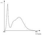
도 3은 본 발명의 실시예에 따른, 발광소자 패키지의 파장에 따른 세기를 나타낸 그래프이다.FIG. 3 is a graph illustrating intensity according to wavelength of a light emitting device package according to an embodiment of the present invention. Referring to FIG.
도 3에 도시된 그래프는, 일반적인 발광소자 패키지의 예시적인 파장 특성을 나타내는 그래프이다.The graph shown in FIG. 3 is a graph showing exemplary wavelength characteristics of a general light emitting device package.
일반적으로 형광체가 사용되지 않은, 발광소자 패키지는 도 3에 도시된 것과 같이 특정 파장의 세기가 강하기 때문에 단색 광원이다. 도 3은 파란색 영역의 파장 세기가 제일 강한 청색 계열의 발광소자 패키지이다.In general, a light emitting device package in which a phosphor is not used is a monochromatic light source because the intensity of a specific wavelength is strong as shown in Fig. 3 is a blue light emitting device package having the strongest wavelength intensity in the blue region.
이러한 발광소자 패키지의 발광 표면에 형광체를 위치시키면, 청색광을 흡수하고 상기 청색광에 의해 여기된 황색광을 방출하므로써, 전체적으로 백색광이 최종적으로 상기 발광소자 패키지에 의해서 발광될 수 있다.When the phosphor is placed on the light emitting surface of the light emitting device package, the white light is finally emitted by the light emitting device package as a whole by absorbing the blue light and emitting the yellow light excited by the blue light.
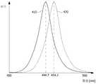
도 4는 본 발명의 실시예에 따른, 두 발광소자 패키지의 파장 특성을 나타낸 그래프이다.4 is a graph showing wavelength characteristics of two light emitting device packages according to an embodiment of the present invention.
도 4를 참조하면, 454.3 [nm]의 제1 주파장을 가지는 파장 특성 그래프(420)과 444.7 [nm]의 제2 주파장을 가지는 파장 특성 그래프(410)이 도시되어 있다.Referring to FIG. 4, there is shown a wavelength
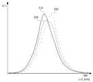
도 5는 본 발명의 실시예에 따른, 도 4의 파장 특성을 이용한 조명 모듈의 파장 특성을 나타낸 그래프이다.5 is a graph illustrating wavelength characteristics of an illumination module using wavelength characteristics of FIG. 4 according to an embodiment of the present invention.
도 5를 참조하면, 본 발명의 실시예에 따라 도 4의 상기 제1 주파장과 상기 제2 주파장을 바탕으로 MRM된 4개의 발광소자 패키지가 배치된 조명 모듈의 파장 특성이 도시되어 있다.Referring to FIG. 5, wavelength characteristics of an illumination module in which four light emitting device packages MRM are arranged based on the first main wavelength and the second main wavelength in FIG. 4 according to an embodiment of the present invention are shown.
제1 조합 그래프(510)은, 상기 제2 주파장을 가지는 3개의 발광소자 패키지와 상기 제1 주파장을 가지는 1개의 발광소재 패키지를 MRM한 조명 모듈의 파장 특성을 나타낸다.The
제2 조합 그래프(520)은, 상기 제2 주파장을 가지는 2개의 발광소자 패키지와 상기 제1 주파장을 가지는 2개의 발광소재 패키지를 MRM한 조명 모듈의 파장 특성을 나타낸다.The
제3 조합 그래프(510)은, 상기 제2 주파장을 가지는 1개의 발광소자 패키지와 상기 제1 주파장을 가지는 3개의 발광소재 패키지를 MRM한 조명 모듈의 파장 특성을 나타낸다.The
주파장 세기의 50% 세기일 때 파장의 폭인 반치폭은 제3 조합 그래프(510)이 가장 크다. 따라서, 가장 반치폭이 큰 제3 조합 그래프(510)가 가리키는 MRM 조합이 가장 CRI 등급이 높을 수 있다.The
도 5에 나타난 것을 예시에 불과하며, 이에 한정되지 않는다.5, the present invention is not limited thereto.
도 5를 참조하면, 주파장의 특성의 조합이 달라지면, 다른 파장 특성의 조명 모듈이 될 수 있다. 따라서, 본 발명의 실시예에 따르면, 다른 주파장 특성의 발광모듈 패키지를 이용하여 다르게 MRM 하면, 다른 파장 특성의 조명 모듈이 될 수 있다.Referring to FIG. 5, if the combination of characteristics of the dominant wavelength is changed, it may be a lighting module having different wavelength characteristics. Therefore, according to the embodiment of the present invention, when the MRM is performed differently using the light emitting module package having different main wavelength characteristics, it can be an illumination module having different wavelength characteristics.
도 6은 본 발명의 다른 실시예에 따른, 발광소자 패키지를 이용한 조명 모듈의 평면도이다.6 is a plan view of an illumination module using a light emitting device package according to another embodiment of the present invention.
도 6을 참조하면, 본 발명의 다른 실시예에 따르면, 복수의 발광소자 패키지는 어느 한 방향으로 나란히 배치될 수 있다.Referring to FIG. 6, according to another embodiment of the present invention, a plurality of light emitting device packages may be arranged side by side in any one direction.
본 발명의 다른 실시예에 따른 조명모듈(600)은 제1 발광소자 패키지(110), 제2 발광소자 패키지(120), 제3 발광소자 패키지(130) 및 제4 발광소자 패키지(140)를 포함할 수 있다.The
제2 발광소자 패키지(120)는 제1 발광소자 패키지(110)의 어느 한 방향에 d5 간격으로 나란히 배치될 수 있다. 제3 발광소자 패키지(130)는 제2 발광소자 패키지(120)의 상기 방향에 d6 간격으로 나란히 배치될 수 있다. 제4 발광소자 패키지(140)는 제3 발광소자 패키지(130)의 상기 방향에 d7 간격으로 나란히 배치될 수 있다.The second light emitting
상기 d5, d6 및 d7는 모두 동일한 250 내지 300 [um] 일 수 있지만, 이것은 예시에 불과하며 이에 한정되지 않는다.The d5, d6, and d7 may all be the same 250 to 300 [mu] m, but this is for exemplary purposes only, and is not limited thereto.
이상 첨부된 도면을 참조하여 본 발명의 실시예들을 설명하였지만, 본 발명이 속하는 기술분야에서 통상의 지식을 가진 자는 본 발명이 그 기술적 사상이나 필수적인 특징을 변경하지 않고서 다른 구체적인 형태로 실시될 수 있다는 것을 이해할 수 있을 것이다. 그러므로 이상에서 기술한 실시예들은 모든 면에서 예시적인 것이며 한정적이 아닌 것으로 이해해야만 한다.While the present invention has been described in connection with what is presently considered to be practical exemplary embodiments, it is to be understood that the invention is not limited to the disclosed embodiments, but, on the contrary, You will understand. It is therefore to be understood that the above-described embodiments are illustrative in all aspects and not restrictive.
100 : 조명 모듈
110 : 제1 발광소자 패키지120 : 제2 발광소자 패키지
130 : 제3 발광소자 패키지140 : 제4 발광소자 패키지100: Lighting module
110: first light emitting device package 120: second light emitting device package
130: third light emitting device package 140: fourth light emitting device package
Claims (7)
Translated fromKorean상기 회로기판 상에 배치되는 파장 특성에 따라 MRM(Multi Rank Mixing)된 복수 개의 발광소자 패키지를 포함하는,
조명모듈.A circuit board; And
And a plurality of light emitting device packages MRM (Multi Rank Mixing) according to wavelength characteristics disposed on the circuit board.
Lighting module.
상기 파장 특성은,
주파장(dominant wavelength)의 값에 의해 구별되는,
조명모듈.The method according to claim 1,
The above-
Which is distinguished by the value of the dominant wavelength,
Lighting module.
제1 주파장과 상기 제1 주파장 보다 짧은 제2 주파장에 의해서 MRMR된 복수 개의 발광소자 패키지를 포함하는,
조명모듈.3. The method of claim 2,
And a plurality of light emitting device packages MRMRed by a first main wavelength and a second main wavelength shorter than the first main wavelength,
Lighting module.
상기 복수 개의 발광소자 패키지는,
적어도 두 개의 파장 특성에 따라 MRM된,
조명모듈.The method according to claim 1,
Wherein the plurality of light emitting device packages include:
The MRM, which is based on at least two wavelength characteristics,
Lighting module.
제1 발광소자 패키지, 제2 발광소자 패키지, 제3 발광소자 패키지 및 제4 발광소자 패키지를 포함하는 4개의 발광소자 패키지가 상기 MRM되어 상기 회로기판 상에 배치된,
조명모듈.The method according to claim 1,
Wherein four light emitting device packages including a first light emitting device package, a second light emitting device package, a third light emitting device package, and a fourth light emitting device package are MRM-mounted on the circuit board,
Lighting module.
상기 제1 발광소자 패키지와 상기 제2 발광소자 패키지는 250 내지 300 [um] 의 간격으로 나란히 배치되고,
상기 제3 발광소자 패키지는 상기 제1 발광소자 패키지의 아래에 250 내지 300 [um] 의 간격으로 배치되며,
상기 제4 발광소자 패키지는 상기 제3 발광소자 패키지의 측면 및 상기 제2 발광소자 패키지의 아래 방향으로 250 내지 300 [um]의 간격으로 배치된,
조명모듈.6. The method of claim 5,
The first light emitting device package and the second light emitting device package are arranged side by side at an interval of 250 to 300 [mu]
Wherein the third light emitting device package is disposed at a distance of 250 to 300 [mu] m below the first light emitting device package,
Wherein the fourth light emitting device package is disposed at a side of the third light emitting device package and in a downward direction of the second light emitting device package at an interval of 250 to 300 [
Lighting module.
상기 제1 발광소자 패키지, 상기 제2 발광소자 패키지, 상기 제3 발광소자 패키지 및 상기 제4 발광소자 패키지는,
어느 한 방향으로 나란히 일정한 간격으로 배치가 되는,
조명모듈.6. The method of claim 5,
The first light emitting device package, the second light emitting device package, the third light emitting device package, and the fourth light emitting device package,
Which are arranged at regular intervals in a certain direction,
Lighting module.
Priority Applications (1)
| Application Number | Priority Date | Filing Date | Title |
|---|---|---|---|
| KR1020160002218AKR102437786B1 (en) | 2016-01-07 | 2016-01-07 | Lighting module using light emitting diode package |
Applications Claiming Priority (1)
| Application Number | Priority Date | Filing Date | Title |
|---|---|---|---|
| KR1020160002218AKR102437786B1 (en) | 2016-01-07 | 2016-01-07 | Lighting module using light emitting diode package |
Publications (2)
| Publication Number | Publication Date |
|---|---|
| KR20170082908Atrue KR20170082908A (en) | 2017-07-17 |
| KR102437786B1 KR102437786B1 (en) | 2022-08-30 |
Family
ID=59443123
Family Applications (1)
| Application Number | Title | Priority Date | Filing Date |
|---|---|---|---|
| KR1020160002218AActiveKR102437786B1 (en) | 2016-01-07 | 2016-01-07 | Lighting module using light emitting diode package |
Country Status (1)
| Country | Link |
|---|---|
| KR (1) | KR102437786B1 (en) |
Citations (5)
| Publication number | Priority date | Publication date | Assignee | Title |
|---|---|---|---|---|
| KR20100057466A (en)* | 2008-11-21 | 2010-05-31 | 엘지이노텍 주식회사 | Light emitting apparatus and fabrication method thereof |
| KR20100076639A (en) | 2008-12-26 | 2010-07-06 | 루미마이크로 주식회사 | Chip on board type led and method manufacturing the same |
| KR20130013458A (en)* | 2011-07-28 | 2013-02-06 | 엘지이노텍 주식회사 | Light emitting device module and lighting system including the same |
| KR101285224B1 (en)* | 2012-05-18 | 2013-07-11 | 우리이앤엘 주식회사 | Chip on board type light emitting module |
| JP2014235859A (en)* | 2013-05-31 | 2014-12-15 | 東芝ライテック株式会社 | Solid lighting device |
- 2016
- 2016-01-07KRKR1020160002218Apatent/KR102437786B1/enactiveActive
Patent Citations (5)
| Publication number | Priority date | Publication date | Assignee | Title |
|---|---|---|---|---|
| KR20100057466A (en)* | 2008-11-21 | 2010-05-31 | 엘지이노텍 주식회사 | Light emitting apparatus and fabrication method thereof |
| KR20100076639A (en) | 2008-12-26 | 2010-07-06 | 루미마이크로 주식회사 | Chip on board type led and method manufacturing the same |
| KR20130013458A (en)* | 2011-07-28 | 2013-02-06 | 엘지이노텍 주식회사 | Light emitting device module and lighting system including the same |
| KR101285224B1 (en)* | 2012-05-18 | 2013-07-11 | 우리이앤엘 주식회사 | Chip on board type light emitting module |
| JP2014235859A (en)* | 2013-05-31 | 2014-12-15 | 東芝ライテック株式会社 | Solid lighting device |
Also Published As
| Publication number | Publication date |
|---|---|
| KR102437786B1 (en) | 2022-08-30 |
Similar Documents
| Publication | Publication Date | Title |
|---|---|---|
| CN102460751B (en) | Solid state lighting device | |
| US9312433B2 (en) | Light emitting element | |
| JP2013540362A (en) | Light emitting device and light emitting method | |
| TWI802587B (en) | Semiconductor device package | |
| JP2011211196A (en) | Light emitting element, and light unit including the same | |
| US8053805B2 (en) | Light emitting device, light emitting device and package, and lighting system | |
| US9281437B2 (en) | Light emitting device, and method for fabricating the same | |
| WO2018132962A1 (en) | Multiple led light source lens design in an integrated package | |
| US9190566B2 (en) | Light emitting device | |
| KR102261945B1 (en) | Light emitting device and lighting apparatus having thereof | |
| KR102607890B1 (en) | Semiconductor device package | |
| US10510925B2 (en) | Light-emitting device and lighting system comprising same | |
| KR20150083248A (en) | Package for light emitting device | |
| KR102437786B1 (en) | Lighting module using light emitting diode package | |
| KR102199983B1 (en) | Light emitting device and light emitting device package having the same | |
| KR100712880B1 (en) | White light emitting diodes can reduce color temperature variations | |
| KR102187484B1 (en) | Light emitting device and lighting system having the same | |
| KR101155033B1 (en) | Led package | |
| CN202111155U (en) | LED package | |
| KR101094127B1 (en) | Light emitting diode package | |
| KR102432034B1 (en) | Semiconductor device package | |
| CN202797078U (en) | LED package and LED display | |
| KR102038441B1 (en) | Lighting device | |
| KR100781285B1 (en) | Lead frame and light emitting device package for light emitting device | |
| KR20180083112A (en) | Substrate and semiconductor device having the same |
Legal Events
| Date | Code | Title | Description |
|---|---|---|---|
| PA0109 | Patent application | Patent event code:PA01091R01D Comment text:Patent Application Patent event date:20160107 | |
| PG1501 | Laying open of application | ||
| A201 | Request for examination | ||
| PA0201 | Request for examination | Patent event code:PA02012R01D Patent event date:20201221 Comment text:Request for Examination of Application Patent event code:PA02011R01I Patent event date:20160107 Comment text:Patent Application | |
| N231 | Notification of change of applicant | ||
| PN2301 | Change of applicant | Patent event date:20210715 Comment text:Notification of Change of Applicant Patent event code:PN23011R01D | |
| E902 | Notification of reason for refusal | ||
| PE0902 | Notice of grounds for rejection | Comment text:Notification of reason for refusal Patent event date:20211211 Patent event code:PE09021S01D | |
| E701 | Decision to grant or registration of patent right | ||
| PE0701 | Decision of registration | Patent event code:PE07011S01D Comment text:Decision to Grant Registration Patent event date:20220628 | |
| GRNT | Written decision to grant | ||
| PR0701 | Registration of establishment | Comment text:Registration of Establishment Patent event date:20220824 Patent event code:PR07011E01D | |
| PR1002 | Payment of registration fee | Payment date:20220825 End annual number:3 Start annual number:1 | |
| PG1601 | Publication of registration |