KR20170080350A - Gate Pulse Modulation Circuit and Display Device Using the same - Google Patents
Gate Pulse Modulation Circuit and Display Device Using the sameDownload PDFInfo
- Publication number
- KR20170080350A KR20170080350AKR1020150191819AKR20150191819AKR20170080350AKR 20170080350 AKR20170080350 AKR 20170080350AKR 1020150191819 AKR1020150191819 AKR 1020150191819AKR 20150191819 AKR20150191819 AKR 20150191819AKR 20170080350 AKR20170080350 AKR 20170080350A
- Authority
- KR
- South Korea
- Prior art keywords
- gate
- output terminal
- resistor
- gate pulse
- output
- Prior art date
- Legal status (The legal status is an assumption and is not a legal conclusion. Google has not performed a legal analysis and makes no representation as to the accuracy of the status listed.)
- Granted
Links
Images


Classifications
- G—PHYSICS
- G09—EDUCATION; CRYPTOGRAPHY; DISPLAY; ADVERTISING; SEALS
- G09G—ARRANGEMENTS OR CIRCUITS FOR CONTROL OF INDICATING DEVICES USING STATIC MEANS TO PRESENT VARIABLE INFORMATION
- G09G3/00—Control arrangements or circuits, of interest only in connection with visual indicators other than cathode-ray tubes
- G09G3/20—Control arrangements or circuits, of interest only in connection with visual indicators other than cathode-ray tubes for presentation of an assembly of a number of characters, e.g. a page, by composing the assembly by combination of individual elements arranged in a matrix no fixed position being assigned to or needed to be assigned to the individual characters or partial characters
- G09G3/22—Control arrangements or circuits, of interest only in connection with visual indicators other than cathode-ray tubes for presentation of an assembly of a number of characters, e.g. a page, by composing the assembly by combination of individual elements arranged in a matrix no fixed position being assigned to or needed to be assigned to the individual characters or partial characters using controlled light sources
- G09G3/30—Control arrangements or circuits, of interest only in connection with visual indicators other than cathode-ray tubes for presentation of an assembly of a number of characters, e.g. a page, by composing the assembly by combination of individual elements arranged in a matrix no fixed position being assigned to or needed to be assigned to the individual characters or partial characters using controlled light sources using electroluminescent panels
- G09G3/32—Control arrangements or circuits, of interest only in connection with visual indicators other than cathode-ray tubes for presentation of an assembly of a number of characters, e.g. a page, by composing the assembly by combination of individual elements arranged in a matrix no fixed position being assigned to or needed to be assigned to the individual characters or partial characters using controlled light sources using electroluminescent panels semiconductive, e.g. using light-emitting diodes [LED]
- G09G3/3208—Control arrangements or circuits, of interest only in connection with visual indicators other than cathode-ray tubes for presentation of an assembly of a number of characters, e.g. a page, by composing the assembly by combination of individual elements arranged in a matrix no fixed position being assigned to or needed to be assigned to the individual characters or partial characters using controlled light sources using electroluminescent panels semiconductive, e.g. using light-emitting diodes [LED] organic, e.g. using organic light-emitting diodes [OLED]
- G09G3/3266—Details of drivers for scan electrodes
- G—PHYSICS
- G09—EDUCATION; CRYPTOGRAPHY; DISPLAY; ADVERTISING; SEALS
- G09G—ARRANGEMENTS OR CIRCUITS FOR CONTROL OF INDICATING DEVICES USING STATIC MEANS TO PRESENT VARIABLE INFORMATION
- G09G3/00—Control arrangements or circuits, of interest only in connection with visual indicators other than cathode-ray tubes
- G09G3/20—Control arrangements or circuits, of interest only in connection with visual indicators other than cathode-ray tubes for presentation of an assembly of a number of characters, e.g. a page, by composing the assembly by combination of individual elements arranged in a matrix no fixed position being assigned to or needed to be assigned to the individual characters or partial characters
- G09G3/34—Control arrangements or circuits, of interest only in connection with visual indicators other than cathode-ray tubes for presentation of an assembly of a number of characters, e.g. a page, by composing the assembly by combination of individual elements arranged in a matrix no fixed position being assigned to or needed to be assigned to the individual characters or partial characters by control of light from an independent source
- G09G3/36—Control arrangements or circuits, of interest only in connection with visual indicators other than cathode-ray tubes for presentation of an assembly of a number of characters, e.g. a page, by composing the assembly by combination of individual elements arranged in a matrix no fixed position being assigned to or needed to be assigned to the individual characters or partial characters by control of light from an independent source using liquid crystals
- G09G3/3611—Control of matrices with row and column drivers
- G09G3/3674—Details of drivers for scan electrodes
- G09G3/3677—Details of drivers for scan electrodes suitable for active matrices only
- G—PHYSICS
- G09—EDUCATION; CRYPTOGRAPHY; DISPLAY; ADVERTISING; SEALS
- G09G—ARRANGEMENTS OR CIRCUITS FOR CONTROL OF INDICATING DEVICES USING STATIC MEANS TO PRESENT VARIABLE INFORMATION
- G09G2310/00—Command of the display device
- G09G2310/02—Addressing, scanning or driving the display screen or processing steps related thereto
- G09G2310/0264—Details of driving circuits
- G09G2310/0291—Details of output amplifiers or buffers arranged for use in a driving circuit
Landscapes
- Engineering & Computer Science (AREA)
- Physics & Mathematics (AREA)
- Computer Hardware Design (AREA)
- General Physics & Mathematics (AREA)
- Theoretical Computer Science (AREA)
- Chemical & Material Sciences (AREA)
- Crystallography & Structural Chemistry (AREA)
- Control Of Indicators Other Than Cathode Ray Tubes (AREA)
Abstract
Translated fromKoreanDescription
Translated fromKorean본 발명은 게이트 펄스 변조 회로 및 이를 이용한 표시장치에 관한 것이다.The present invention relates to a gate pulse modulation circuit and a display device using the same.
정보화 기술이 발달함에 따라 사용자와 정보간의 연결 매체인 표시장치의 시장이 커지고 있다. 이에 따라, 유기전계발광표시장치(Organic Light Emitting Display: OLED), 액정표시장치(Liquid Crystal Display: LCD) 및 플라즈마표시장치(Plasma Display Panel: PDP) 등과 같은 표시장치의 사용이 증가하고 있다.As the information technology is developed, the market of display devices, which is a connection medium between users and information, is getting larger. Accordingly, the use of display devices such as an organic light emitting display (OLED), a liquid crystal display (LCD), and a plasma display panel (PDP) is increasing.
앞서 설명한 표시장치 중 일부 예컨대, 액정표시장치나 유기전계발광표시장치는 표시패널에 포함된 서브 픽셀들에 게이트신호 및 데이터신호 등이 공급되면, 선택된 서브 픽셀이 발광을 하게 됨으로써 영상을 표시할 수 있다.Some of the above-described display devices, for example, a liquid crystal display device and an organic light emitting display device, are capable of displaying images when a gate signal and a data signal are supplied to subpixels included in a display panel, have.
위와 같은 표시장치는 복수의 서브 픽셀을 포함하는 표시패널과 표시패널을 구동하는 구동부가 포함된다. 구동부에는 표시패널에 게이트신호(또는 스캔신호)를 공급하는 게이트 구동부 및 표시패널에 데이터신호를 공급하는 데이터 구동부 등이 포함된다.Such a display apparatus includes a display panel including a plurality of sub-pixels and a driver for driving the display panel. The driver includes a gate driver for supplying a gate signal (or a scan signal) to the display panel, and a data driver for supplying a data signal to the display panel.
게이트 구동부는 집적회로 형태뿐만 아니라 박막 트랜지스터 공정과 함께 게이트인패널(Gate In Panel; GIP) 형태로 표시패널에 형성되는 표시패널 내장형으로 이루어지기도 한다.The gate driver may be a built-in display panel built in a display panel in the form of a gate in panel (GIP) together with a thin film transistor process as well as an integrated circuit type.
표시장치는 장치의 소비전류를 절감 및 개선하기 위하여, 게이트신호를 구성하는 게이트 전압의 레벨을 가변하는 게이트 펄스 변조(Gate Pulse Modulation; GPM) 회로를 사용한다. 그런데 종래에 제안된 게이트 변조 방식은 개선 사항이 존재하고 있는바 이에 대한 연구가 진행되고 있다.The display apparatus uses a gate pulse modulation (GPM) circuit for varying the level of the gate voltage constituting the gate signal in order to reduce and improve the consumption current of the apparatus. However, there are improvements in the conventional gate modulation method, and research is underway.
상술한 배경기술의 문제점을 해결하기 위한 본 발명은 게이트 펄스 변조 회로의 하강 정지 레벨(Falling Stop Level)의 정확성과 구동 정밀도를 향상하는 것이다. 또한, 본 발명은 게이트 펄스 변조 회로의 구동 정밀도를 높여 표시패널의 화면 양단의 어두움 또는 게이트 구동부들 간의 휘도차에 따른 게이트 블록 딤(Gate Block Dim) 등이 유발되는 문제를 해소 및 개선하는 것이다.SUMMARY OF THE INVENTION The present invention for solving the above problems of the background art is to improve accuracy and driving precision of a falling stop level of a gate pulse modulation circuit. The present invention also improves the driving precision of the gate pulse modulation circuit and solves and improves problems such as darkness at both ends of the screen of the display panel or gate block dim due to the difference in luminance between the gate drivers.
상술한 과제 해결 수단으로 본 발명은 스위치 회로부 및 로직 회로부를 포함하는 게이트 펄스 변조 회로를 제공한다. 스위치 회로부는 게이트 전압을 그대로 또는 가변하여 자신의 출력단자를 통해 출력하기 위한 스위칭 동작을 수행한다. 로직 회로부는 외부로부터 공급된 제어신호에 대응하여 스위치 회로부를 제어하기 위한 스위치 제어신호를 출력한다. 스위치 회로부는 자신의 출력단자를 통해 출력된 게이트 전압의 폴링 에지를 참조전압으로 방전시킨다.The present invention provides a gate pulse modulation circuit including a switch circuit portion and a logic circuit portion. The switch circuit unit performs a switching operation to directly or vary the gate voltage and to output it through its own output terminal. The logic circuit portion outputs a switch control signal for controlling the switch circuit portion in response to a control signal supplied from the outside. The switch circuit part discharges the falling edge of the gate voltage output through its output terminal to the reference voltage.
참조전압을 스위치 회로부에 전달하는 저항기를 포함할 수 있다.And a resistor for transmitting the reference voltage to the switch circuit portion.
참조전압을 버퍼링하여 저항기에 전달하는 버퍼 회로부를 포함할 수 있다.And buffer circuitry for buffering the reference voltage and delivering it to the resistor.
버퍼 회로부는 참조전압을 전달하는 참조전압라인에 입력단자가 연결되고 저항기의 일단에 출력단자가 연결될 수 있다.In the buffer circuit portion, an input terminal is connected to a reference voltage line for transmitting a reference voltage, and an output terminal is connected to one end of the resistor.
버퍼 회로부는 외부 또는 내부 레지스터값에 따라 게이트 전압의 방전 레벨과 방전 기울기를 가변하는 가변저항기들을 포함할 수 있다.The buffer circuitry may include variable resistors that vary the discharge level and discharge slope of the gate voltage according to external or internal register values.
버퍼 회로부는 외부 또는 내부 레지스터값에 따라 저항값이 가변되는 제1가변저항기와 제2가변저항기를 포함하고, 제1가변저항기는 버퍼 회로부의 반전단자에 일단이 연결되고 버퍼 회로부의 출력단자에 타단이 연결되며, 제2가변저항기는 버퍼 회로부의 출력단자에 일단이 연결되고 저항기의 일단에 타단이 연결될 수 있다.The buffer circuit section includes a first variable resistor and a second variable resistor whose resistance values are variable according to external or internal register values. The first variable resistor has one end connected to the inverting terminal of the buffer circuit section, And the second variable resistor may have one end connected to the output terminal of the buffer circuit unit and the other end connected to one end of the resistor.
제1가변저항기와 제2가변저항기의 저항비율은 M:N(M은 1 이상 정수, N은 2 이상 정수이며, M < N)일 수 있다.The resistance ratio of the first variable resistor and the second variable resistor may be M: N (M is an integer of 1 or more, N is an integer of 2 or more, and M < N).
다른 측면에서 본 발명은 표시패널, 전원 공급부 및 게이트 구동부를 포함하는 표시장치를 제공한다. 표시패널은 영상을 표시한다. 전원 공급부는 게이트 전압을 그대로 또는 가변하여 출력하는 게이트 펄스 변조 회로를 포함한다. 게이트 구동부는 전원 공급부로부터 출력된 게이트 전압을 기반으로 표시패널에 공급할 게이트신호를 마련한다. 게이트 펄스 변조 회로는 게이트 전압을 그대로 또는 가변하여 자신의 출력단자를 통해 출력하기 위한 스위칭 동작을 수행하는 스위치 회로부와, 외부로부터 공급된 제어신호에 대응하여 스위치 회로부를 제어하기 위한 스위치 제어신호를 출력하는 로직 회로부를 포함하고, 스위치 회로부는 자신의 출력단자를 통해 출력된 게이트 전압의 폴링 에지를 참조전압으로 방전시킬 수 있다.In another aspect, the present invention provides a display device including a display panel, a power supply, and a gate driver. The display panel displays the image. The power supply unit includes a gate pulse modulation circuit that outputs the gate voltage as it is or changes it. The gate driver provides a gate signal to supply the display panel based on the gate voltage output from the power supply. The gate pulse modulation circuit outputs a switch control signal for controlling the switch circuit section in response to a control signal supplied from the outside, And the switch circuit portion can discharge the falling edge of the gate voltage output through its output terminal to a reference voltage.
참조전압을 스위치 회로부에 전달하는 저항기와, 참조전압을 버퍼링하여 저항기에 전달하는 버퍼 회로부를 포함할 수 있다.A resistor for transmitting the reference voltage to the switch circuit portion, and a buffer circuit portion for buffering the reference voltage and transmitting the buffered voltage to the resistor.
버퍼 회로부는 외부 또는 내부 레지스터값에 따라 저항값이 가변되는 제1가변저항기와 제2가변저항기를 포함하고, 제1가변저항기는 버퍼 회로부의 반전단자에 일단이 연결되고 버퍼 회로부의 출력단자에 타단이 연결되며, 제2가변저항기는 버퍼 회로부의 출력단자에 일단이 연결되고 저항기의 일단에 타단이 연결될 수 있다.The buffer circuit section includes a first variable resistor and a second variable resistor whose resistance values are variable according to external or internal register values. The first variable resistor has one end connected to the inverting terminal of the buffer circuit section, And the second variable resistor may have one end connected to the output terminal of the buffer circuit unit and the other end connected to one end of the resistor.
본 발명은 게이트 펄스 변조 회로의 구성 및 동작을 단순화함과 더불어 신호 지연 문제 등을 해소하여 전압 레벨 가변시 하강 정지 레벨(Falling Stop Level)의 정확성과 구동 정밀도를 향상할 수 있는 효과가 있다. 또한, 본 발명은 게이트 펄스 변조 회로의 구동 정밀도를 높여 표시패널의 화면 양단의 어두움 또는 게이트 구동부들 간의 휘도차에 따른 게이트 블록 딤(Gate Block Dim) 등이 유발되는 문제를 해소 및 개선할 수 있는 효과가 있다.The present invention simplifies the configuration and operation of the gate pulse modulation circuit, eliminates the signal delay problem, and improves the accuracy of the falling stop level and the driving precision when the voltage level is varied. In addition, the present invention can improve the driving precision of the gate pulse modulation circuit and solve or improve the problem of darkness at both ends of the screen of the display panel or gate block dim due to the luminance difference between the gate drivers It is effective.
도 1은 표시장치의 개략적인 블록도.
도 2는 도 1에 도시된 서브 픽셀의 구성 예시도.
도 3은 본 발명의 제1실시예에 따른 전원 공급부의 개략적인 구성 예시도.
도 4는 실험예에 따른 게이트 펄스 변조부의 구성도.
도 5a 내지 도 5c는 실험예에 따른 게이트 펄스 변조부의 동작 순서를 설명하기 위한 도면들.
도 6은 실험예에 따른 게이트 펄스 변조부의 문제점을 설명하기 위한 파형도.
도 7은 본 발명의 제1실시예에 따른 게이트 펄스 변조부의 구성도.
도 8a 및 도 8b는 본 발명의 제1실시예에 따른 게이트 펄스 변조부의 동작 순서를 설명하기 위한 도면들.
도 9는 본 발명의 제1실시예에 따른 게이트 펄스 변조부의 개선점을 설명하기 위한 파형도.
도 10은 본 발명의 제2실시예에 따른 게이트 펄스 변조부의 구성도.
도 11a 및 도 11b는 본 발명의 제2실시예에 따른 게이트 펄스 변조부의 동작 순서를 설명하기 위한 도면들.
도 12는 본 발명의 제2실시예에 따른 게이트 펄스 변조부의 개선점을 설명하기 위한 파형도.
도 13 및 도 14는 버퍼 회로부의 구성 예시도들.
도 15 및 도 16은 버퍼 회로부의 구성에 따른 출력 파형도들.1 is a schematic block diagram of a display device;
FIG. 2 is a diagram illustrating a configuration example of a subpixel shown in FIG. 1; FIG.
3 is a schematic configuration example of a power supply unit according to the first embodiment of the present invention.
4 is a configuration diagram of a gate pulse modulation unit according to an experimental example;
5A to 5C are diagrams for explaining the operation sequence of the gate pulse modulation unit according to the experimental example.
6 is a waveform diagram for explaining a problem of a gate pulse modulator according to an experimental example;
7 is a configuration diagram of a gate pulse modulation unit according to the first embodiment of the present invention;
8A and 8B are diagrams for explaining the operation sequence of the gate pulse modulator according to the first embodiment of the present invention.
9 is a waveform diagram for explaining improvement of the gate pulse modulation unit according to the first embodiment of the present invention;
10 is a configuration diagram of a gate pulse modulation unit according to a second embodiment of the present invention;
11A and 11B are diagrams for explaining the operation sequence of the gate pulse modulator according to the second embodiment of the present invention.
12 is a waveform diagram for explaining improvement of the gate pulse modulation unit according to the second embodiment of the present invention;
Figs. 13 and 14 are exemplary configuration diagrams of a buffer circuit section. Fig.
15 and 16 are output waveform diagrams according to the configuration of the buffer circuit section.
이하, 본 발명의 실시를 위한 구체적인 내용을 첨부된 도면을 참조하여 설명한다.DETAILED DESCRIPTION OF THE PREFERRED EMBODIMENTS Hereinafter, embodiments of the present invention will be described in detail with reference to the accompanying drawings.
본 발명에 따른 표시장치는 텔레비젼, 셋톱박스, 네비게이션, 영상 플레이어, 블루레이 플레이어, 개인용 컴퓨터(PC), 홈시어터 및 모바일폰 등으로 구현된다. 표시장치는 액정표시장치, 유기전계발광표시장치, 양자점표시장치, 전기영동표시장치, 플라즈마표시장치 등이 선택될 수 있으나 이에 한정되지 않는다.The display device according to the present invention is implemented as a television, a set-top box, a navigation device, a video player, a Blu-ray player, a personal computer (PC), a home theater and a mobile phone. The display device may be a liquid crystal display device, an organic light emitting display device, a quantum dot display device, an electrophoretic display device, a plasma display device, or the like, but is not limited thereto.
이하에서 설명되는 트랜지스터는 게이트전극을 제외하고 타입에 따라 소오스전극과 드레인전극 또는 드레인전극과 소오스전극으로 명명될 수 있는바, 이를 한정하지 않기 위해 제1전극과 제2전극으로 설명한다.The transistor described below may be referred to as a source electrode, a drain electrode, a drain electrode, and a source electrode, depending on the type, except for the gate electrode. However, the transistor will be described as a first electrode and a second electrode.
도 1은 표시장치의 개략적인 블록도이고, 도 2는 도 1에 도시된 서브 픽셀의 구성 예시도이며, 도 3은 본 발명의 제1실시예에 따른 전원 공급부의 개략적인 구성 예시도이다.FIG. 1 is a schematic block diagram of a display device, FIG. 2 is a configuration example of a subpixel shown in FIG. 1, and FIG. 3 is a schematic configuration diagram of a power supply unit according to a first embodiment of the present invention.
도 1 및 도 2에 도시된 바와 같이, 표시장치에는 표시패널(100), 타이밍 제어부(110), 데이터 구동부(120), 전원 공급부(130) 및 게이트 구동부(140A, 140B)가 포함된다.1 and 2, a display device includes a
표시패널(100)에는 상호 교차하는 데이터 라인들(DL) 및 게이트 라인들(GL)에 구분되어 연결된 서브 픽셀들이 포함된다. 표시패널(100)은 적어도 하나의 필름이나 기판 그리고 그 위에 형성된 서브 픽셀들을 수분이나 산소 등의 외기로부터 보호하기 위해 밀봉된다.The
표시패널(100)은 서브 픽셀들이 형성되는 표시영역(AA)과 표시영역(AA)의 외측으로 각종 신호라인들이나 패드 등이 형성되는 비표시영역(LNA, RNA)을 포함한다. 표시패널(100)은 서브 픽셀(SP)의 구성 방식에 따라 액정층이나 유기 발광층을 포함하는 형태로 구현된다.The
하나의 서브 픽셀(SP)에는 게이트 라인(GL1)과 데이터 라인(DL1)에 연결된 스위칭 트랜지스터(SW)와 스위칭 트랜지스터(SW)를 통해 공급된 게이트신호에 대응하여 공급된 데이터신호(DATA)에 대응하여 동작하는 픽셀회로(PC)가 포함된다. 서브 픽셀(SP)은 픽셀회로(PC)의 구성에 따라 액정층을 구동하거나 유기 발광층 등을 구동하기 위한 회로로 구현된다.One subpixel SP corresponds to the supplied data signal DATA corresponding to the gate signal supplied through the switching transistor SW and the switching transistor SW connected to the gate line GL1 and the data line DL1 And a pixel circuit (PC) that operates by the pixel circuit. The subpixel SP is implemented as a circuit for driving the liquid crystal layer or for driving the organic light emitting layer or the like in accordance with the configuration of the pixel circuit PC.
타이밍 제어부(110)는 영상보드에 연결된 LVDS 또는 TMDS 인터페이스 수신회로 등을 통해 수직 동기신호, 수평 동기신호, 데이터 인에이블 신호, 도트 클럭 등의 타이밍신호를 입력받는다. 타이밍 제어부(110)는 입력된 타이밍신호를 기준으로 데이터 구동부(120)와 게이트 구동부(140A, 140B)의 동작 타이밍을 제어하기 위한 타이밍 제어신호들을 발생한다.The
데이터 구동부(120)는 다수의 소스 드라이브 IC(Integrated Circuit)들을 포함한다. 소스 드라이브 IC들은 타이밍 제어부(110)로부터 데이터신호(DATA)와 소스 타이밍 제어신호(DDC)를 공급받는다. 소스 드라이브 IC들은 소스 타이밍 제어신호(DDC)에 응답하여 데이터신호(DATA)를 디지털신호에서 아날로그신호로 변환하고, 이를 표시패널(100)의 데이터 라인들(DL)을 통해 공급한다. 소스 드라이브 IC들은 COG(Chip On Glass) 공정이나 TAB(Tape Automated Bonding) 공정에 의해 표시패널(100)의 데이터 라인들(DL)에 접속된다.The
게이트 구동부(140A, 140B)는 게이트인패널(Gate In Panel; 이하 GIP) 방식에 의해 표시패널(100)에 박막 트랜지스터 형태로 형성되거나 집적회로(IC) 형태로 형성된다. 게이트 구동부(140A, 140B)는 표시패널(100)의 좌측 및 우측 비표시영역(LNA, RNA)에 구분되어 형성되거나 인쇄회로기판 또는 연성회로기판 등에 실장된다.The
게이트 구동부(140A, 140B)는 전원 공급부(130)로부터 출력된 신호나 전압 등(CLK, VST, RST, VGH, VGL)을 기반으로 게이트신호를 시프트하고 출력한다. 게이트 구동부(140A, 140B)는 서브 픽셀들에 포함된 스위칭 트랜지스터들을 턴온 또는 턴오프할 수 있는 전압 레벨로 게이트신호를 마련한다.The
전원 공급부(130)는 타이밍 제어부(110)의 제어하에 클록신호라인, 스타트신호라인, 전압라인 등을 통해 공급되는 클록신호(CLK), 스타트신호(VST), 리셋신호(RST), 게이트하이전압(VGH) 및 게이트로우전압(VGL) 등의 레벨을 시프팅한 후 게이트 구동부(140A, 140B)에 공급한다.The
도 1 및 도 3에 도시된 바와 같이, 전원 공급부(130)는 게이트 펄스 변조부(135)(Gate Pulse Modulation; GPM 또는 GPM 회로) 및 게이트 전압 출력부(139)를 포함한다. 게이트 전압 출력부(139)는 게이트하이전압(VGH)과 게이트로우전압(VGL)을 출력한다. 게이트 펄스 변조부(135)는 게이트 전압 출력부(139)를 통해 출력되는 게이트 전압들(VGH, VGL) 중 하나의 전압 레벨을 변조하여 출력한다.1 and 3, the
게이트 펄스 변조부(135)는 타이밍 제어부(110)로부터 출력된 제어신호(CS)에 대응하여 게이트 전압 출력부(139)를 통해 출력되는 게이트 전압들(VGH, VGL) 중 하나의 전압 레벨을 변조하여 출력한다. 게이트 펄스 변조부(135)는 장치의 소비전류를 개선 및 절감하기 위해 게이트 전압 출력부(139)를 통해 출력되는 게이트 전압들(VGH, VGL) 중 하나의 라이징 에지나 폴링 에지 중 하나 이상을 가변한다.The
게이트 펄스 변조부(135)는 도시된 바와 같이 전원 공급부(130)와 통합되거나 독립적인 IC로 구성될 수 있다. 그러나 이하에서는 설명의 편의를 위해 전원 공급부(130) 내에 게이트 펄스 변조부(135)가 포함된 것을 일례로 설명한다. 또한, 게이트 펄스 변조부(135)는 게이트하이전압(VGH)의 폴링 에지의 레벨을 변조하여 출력하는 것을 일례로 설명한다.The
<실험예><Experimental Example>
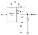
도 4는 실험예에 따른 게이트 펄스 변조부의 구성도이고, 도 5a 내지 도 5c는 실험예에 따른 게이트 펄스 변조부의 동작 순서를 설명하기 위한 도면들이며, 도 6은 실험예에 따른 게이트 펄스 변조부의 문제점을 설명하기 위한 파형도이다.FIG. 4 is a configuration diagram of a gate pulse modulation unit according to an experimental example, FIGS. 5A to 5C are diagrams for explaining an operation procedure of a gate pulse modulation unit according to an experimental example, Fig.
도 4에 도시된 바와 같이, 실험예에 따른 게이트 펄스 변조부(135)는 로직 회로부(131), 비교 회로부(132), 노이즈 필터부(133) 및 스위치 회로부(134)를 포함한다.4, the gate
로직 회로부(131)는 타이밍 제어부로부터 출력된 제어신호(CS)와 비교 회로부(132)로부터 출력된 비교 결과에 대응하여 스위치 회로부(134)를 제어하는 스위치 제어신호(Q1C, Q2C)를 출력한다.The
비교 회로부(132)는 노이즈 필터부(133)로부터 출력된 참조전압(Ref)과 피드백전압(F/B)을 비교하여 결과값을 출력한다. 비교 회로부(132)로부터 출력된 결과값은 게이트하이전압의 폴링 에지 가변시 폴링 에지의 하강 정지 시점을 결정하는 인자로 사용된다.The
노이즈 필터부(133)는 비교 회로부(132)의 비교 동작시 참조전압(Ref)과 피드백전압(F/B)에 형성될 수 있는 노이즈를 제거한다. 노이즈 필터부(133)는 참조전압라인에 제1단자가 연결되고 피드백라인에 제2단자가 연결된다. 피드백라인은 게이트 펄스 변조부의 출력단자에 연결된다.The
스위치 회로부(134)는 로직 회로부(131)로부터 출력된 스위치 제어신호(Q1C, Q2C)에 대응하여 게이트하이전압(VGH)을 그대로 출력하거나 게이트하이전압(VGH)의 폴링 에지를 가변하여 출력하기 위한 스위칭 동작을 한다.The
스위치 회로부(134)는 게이트 펄스 변조부(135)의 게이트하이전압단자(VGH)와 입출력단자(RE) 사이에 배치된 제1스위치(Q1)와 제2스위치(Q2)를 포함한다. 제1스위치(Q1)는 게이트 펄스 변조부(135)의 게이트하이전압단자(VGH)에 제1전극이 연결되고 게이트 펄스 변조부(135)의 출력단자(GPM출력)에 제2전극이 연결되고 제어신호라인에 게이트전극이 연결된다. 제2스위치(Q2)는 게이트 펄스 변조부(135)의 입출력단자(RE)에 제1전극이 연결되고 게이트 펄스 변조부(135)의 출력단자(GPM출력)에 제2전극이 연결되고 제어신호라인에 게이트전극이 연결된다.The
저항기(R1)는 게이트 펄스 변조부(135)의 입출력단자(RE)(제2스위치의 제1전극)에 타단이 연결되고 그라운드전압라인(GND)에 일단이 연결된다. 커패시터(C1)는 게이트 펄스 변조부(135)의 출력단자(GPM출력)에 일단이 연결되고 그라운드전압라인(GND)에 타단이 연결된다. 커패시터(C1)는 게이트 펄스 변조부(135)의 출력단자(GPM출력)를 통해 출력되는 전압을 일정시간 유지하는 역할을 한다.The other end of the resistor R1 is connected to the input / output terminal RE of the gate pulse modulator 135 (the first electrode of the second switch), and one end of the resistor R1 is connected to the ground voltage line GND. The capacitor C1 is connected at one end to the output terminal (GPM output) of the
실험예에 따른 게이트 펄스 변조부(135)는 도 5a, 도 5b 및 도 5c의 순서로 동작한다. 게이트 펄스 변조부(135)의 동작에 따른 출력은 GPM 출력을 나타내는 도 6을 참조한다.The
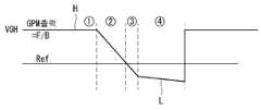
도 5a 및 도 6에 도시된 바와 같이, 제1스위치(Q1)가 턴온되고 제2스위치(Q2)가 턴오프되면 게이트하이전압(VGH)은 그대로 출력된다. 즉, 게이트 펄스 변조부(135)는 게이트하이전압(VGH)의 폴링 에지를 변조하지 않고 그대로 출력한다. (도 6의 ① 구간 참조)As shown in Figs. 5A and 6, when the first switch Q1 is turned on and the second switch Q2 is turned off, the gate high voltage VGH is output as it is. That is, the
도 5b 및 도 6에 도시된 바와 같이, 제1스위치(Q1)가 턴오프되고 제2스위치(Q2)가 턴온되면 이전에 출력된 게이트하이전압(VGH)은 저항기(R1) 및 그라운드전압라인(GND)을 통해 일정시간 동안 방전이 일어난다. 이에 따라, 게이트하이전압(VGH)은 로직하이(H)에서 로직로우(L)로 떨어지게 된다. (도 6의 ② 구간 참조)As shown in FIGS. 5B and 6, when the first switch Q1 is turned off and the second switch Q2 is turned on, the previously outputted gate high voltage VGH is supplied to the resistor R1 and the ground voltage line GND) for a certain period of time. As a result, the gate high voltage VGH falls from a logic high H to a logic low L. [ (See section (2) in Fig. 6)
게이트 펄스 변조부(135)는 참조전압(Ref)과 피드백전압(F/B)을 공급받는다. 참조전압(Ref)과 피드백전압(F/B)은 노이즈 필터부(133)를 거친 후 비교 회로부(132)에 의해 비교된 후 결과값을 생성 및 출력하므로 신호 지연이 발생한다. 이에 따라, 게이트하이전압(VGH)은 참조전압(Ref)보다 낮은 로직로우(L) 레벨로 떨어지게 된다. (도 6의 ③ 구간 참조)The
도 5c 및 도 6에 도시된 바와 같이, 참조전압(Ref)과 피드백전압(F/B)이 같다는 결과값에 의해 제1스위치(Q1)와 제2스위치(Q2)가 턴오프되면 게이트하이전압(VGH)은 출력되지 않는다. 즉, 게이트 펄스 변조부(135)의 출력단자(GPM출력)는 플로팅(floating) 상태가 됨과 더불어 커패시터(C1)에 충전된 전압으로 유지 및 자연 방전된다. (도 6의 ④ 구간 참조)When the first switch Q1 and the second switch Q2 are turned off by the result that the reference voltage Ref and the feedback voltage F / B are equal to each other as shown in Figs. 5C and 6, (VGH) is not output. In other words, the output terminal (GPM output) of the
이상과 같은 구성에 의해, 실험예에 따른 게이트 펄스 변조부(135)는 게이트 펄스 변조의 하강 정지(GPM Falling Stop) 동작 이후 출력을 플로팅 상태로 유지한다.With the above configuration, the gate
그런데 실험예에 따른 게이트 펄스 변조부(135)는 참조전압(Ref)과 피드백전압(F/B) 간의 비교시 노이즈 필터로 인한 지연과 비교 동작시의 지연으로 인하여 참조전압(Ref) 대비 출력전압이 하강하는 문제가 있다. 또한, 게이트 펄스 변조부(135)의 출력단자(GPM출력)가 플로팅된 이후 커패시터(C1)의 자연 방전으로 인한 전압 레벨의 하강이 유발된다. (도 6 참조)However, the
그 결과, 실험예에 따른 게이트 펄스 변조부(135)는 게이트하이전압(VGH)의 레벨 가변시 하강 정지 레벨(Falling Stop Level)이 부정확하고 정밀도가 떨어진다. 또한, 실험예에 따른 게이트 펄스 변조부(135)를 갖는 전원 공급부(130)는 위의 문제로 인하여 표시패널의 화면 양단의 어두움 또는 게이트 구동부들 간의 휘도차에 따른 게이트 블록 딤(Gate Block Dim) 등이 유발된다.As a result, in the
<제1실시예>≪
도 7은 본 발명의 제1실시예에 따른 게이트 펄스 변조부의 구성도이고, 도 8a 및 도 8b는 본 발명의 제1실시예에 따른 게이트 펄스 변조부의 동작 순서를 설명하기 위한 도면들이며, 도 9는 본 발명의 제1실시예에 따른 게이트 펄스 변조부의 개선점을 설명하기 위한 파형도이다.FIG. 7 is a configuration diagram of a gate pulse modulation unit according to the first embodiment of the present invention, FIGS. 8A and 8B are diagrams for explaining the operation sequence of the gate pulse modulation unit according to the first embodiment of the present invention, Is a waveform diagram for explaining an improvement of the gate pulse modulation unit according to the first embodiment of the present invention.
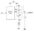
도 7에 도시된 바와 같이, 본 발명의 제1실시예에 따른 게이트 펄스 변조부(135)는 로직 회로부(131) 및 스위치 회로부(134)를 포함한다.7, the
로직 회로부(131)는 타이밍 제어부로부터 출력된 제어신호(CS)를 기반으로 스위치 회로부(134)를 제어하는 스위치 제어신호(Q1C, Q2C)를 출력한다.The
스위치 회로부(134)는 로직 회로부(131)로부터 출력된 스위치 제어신호(Q1C, Q2C)에 대응하여 게이트하이전압(VGH)을 그대로 출력하거나 게이트하이전압(VGH)의 폴링 에지를 가변하여 출력하기 위한 스위칭 동작을 한다.The
스위치 회로부(134)는 게이트 펄스 변조부(135)의 게이트하이전압단자(VGH)와 입출력단자(RE) 사이에 배치된 제1스위치(Q1)와 제2스위치(Q2)를 포함한다.The
제1스위치(Q1)는 게이트 펄스 변조부(135)의 게이트하이전압단자(VGH)에 제1전극이 연결되고 게이트 펄스 변조부(135)의 출력단자(GPM출력)에 제2전극이 연결되고 제어신호라인에 게이트전극이 연결된다.The first switch Q1 has a first electrode connected to the gate high voltage terminal VGH of the
제2스위치(Q2)는 게이트 펄스 변조부(135)의 입출력단자(RE)에 제1전극이 연결되고 게이트 펄스 변조부(135)의 출력단자(GPM출력)에 제2전극이 연결되고 제어신호라인에 게이트전극이 연결된다.The second switch Q2 has the first electrode connected to the input / output terminal RE of the
저항기(R1)는 게이트 펄스 변조부(135)의 입출력단자(RE)(제2스위치의 제1전극)에 타단이 연결되고 참조전압라인에 일단이 연결된다. 커패시터(C1)는 게이트 펄스 변조부(135)의 출력단자(GPM출력)에 일단이 연결되고 그라운드전압라인(GND)에 타단이 연결된다. 커패시터(C1)는 게이트 펄스 변조부(135)의 출력단자(GPM출력)를 통해 출력되는 전압을 일정시간 유지하는 역할을 한다.The other end of the resistor R1 is connected to the input / output terminal RE of the gate pulse modulator 135 (the first electrode of the second switch), and one end is connected to the reference voltage line. The capacitor C1 is connected at one end to the output terminal (GPM output) of the
제1실시예는 실험예에서 유발되는 문제점을 해소하기 위해 게이트 펄스 변조부(135) 내에서 노이즈 필터부와 비교 회로부를 제거한다. 대신, 저항기(R1)의 일단을 참조전압라인에 연결한다. 게이트 펄스 변조부(135)의 입출력단자(RE)에 저항기(R1)의 타단을 연결하고 저항기(R1)의 일단에 참조전압라인을 연결하면, 참조전압(Ref)을 기반으로 방전을 유도할 수 있다.The first embodiment removes the noise filter portion and the comparison circuit portion in the
제1실시예에 따른 게이트 펄스 변조부(135)는 도 8a 및 도 8b의 순서로 동작한다. 게이트 펄스 변조부(135)의 동작에 따른 출력은 GPM 출력을 나타내는 도 9를 참조한다.The
도 8a 및 도 9에 도시된 바와 같이, 제1스위치(Q1)가 턴온되고 제2스위치(Q2)가 턴오프되면 게이트하이전압(VGH)은 그대로 출력된다. 즉, 게이트 펄스 변조부(135)는 게이트하이전압(VGH)의 폴링 에지를 변조하지 않고 그대로 출력한다. (도 9의 ① 구간 참조)As shown in Figs. 8A and 9, when the first switch Q1 is turned on and the second switch Q2 is turned off, the gate high voltage VGH is output as it is. That is, the
도 8b 및 도 9에 도시된 바와 같이, 제1스위치(Q1)가 턴오프되고 제2스위치(Q2)가 턴온되면 이전에 출력된 게이트하이전압(VGH)은 저항기(R1)를 통해 일정시간 동안 방전이 일어난다. 이때, 게이트 펄스 변조부(135)의 출력단자(GPM출력)의 전압 레벨은 참조전압(Ref)과 동일한 전압(GPM출력 = Ref)이 형성된다이 형성된다. 이에 따라, 게이트하이전압(VGH)은 로직하이(H)에서 참조전압(Ref)과 등전위 레벨에 해당하는 로직로우(L)로 떨어지게 된다. (도 9의 ② 구간 참조)8B and 9, when the first switch Q1 is turned off and the second switch Q2 is turned on, the previously outputted gate high voltage VGH is supplied to the first switch Q1 through the resistor R1 for a predetermined time Discharge occurs. At this time, the voltage level of the output terminal (GPM output) of the
제1실시예에 따른 게이트 펄스 변조부(135)는 참조전압(Ref)을 기반으로 게이트하이전압(VGH)을 가변하기 위한 방전이 수행되므로 도 6의 ③ 구간과 같은 신호 지연이 발생하지 않는다. 또한, 게이트 펄스 변조부(135)의 출력단자(GPM출력)는 도 6의 ④ 구간과 같이 플로팅(floating) 상태가 되지 않고 참조전압(Ref)으로 유지 및 방전(플로팅에 의한 자연 방전 없음)된다.The
이상과 같은 구성에 의해, 제1실시예에 따른 게이트 펄스 변조부(135)는 회로의 구성 및 동작을 단순화하여 신호 지연 문제 등을 해소하고 전압 출력 이후 커패시터(C1)의 자연 방전으로 인한 전압 레벨의 하강이 유발되지 않도록 참조전압(Ref)과 등전위로 출력전압을 유지한다.With the above configuration, the
그 결과, 제1실시예에 따른 게이트 펄스 변조부(135)는 게이트하이전압(VGH)의 레벨 가변시 하강 정지 레벨(Falling Stop Level)의 정확성과 구동 정밀도를 향상할 수 있다. 또한, 제1실시예에 따른 게이트 펄스 변조부(135)를 갖는 전원 공급부(130)는 구동 정밀도를 높여 표시패널의 화면 양단의 어두움 또는 게이트 구동부들 간의 휘도차에 따른 게이트 블록 딤(Gate Block Dim) 등이 유발되는 문제를 해소 및 개선할 수 있다.As a result, the
<제2실시예>≪
도 10은 본 발명의 제2실시예에 따른 게이트 펄스 변조부의 구성도이고, 도 11a 및 도 11b는 본 발명의 제2실시예에 따른 게이트 펄스 변조부의 동작 순서를 설명하기 위한 도면들이며, 도 12는 본 발명의 제2실시예에 따른 게이트 펄스 변조부의 개선점을 설명하기 위한 파형도이다.FIG. 10 is a configuration diagram of a gate pulse modulation unit according to the second embodiment of the present invention, FIGS. 11A and 11B are diagrams for explaining the operation sequence of the gate pulse modulation unit according to the second embodiment of the present invention, Is a waveform diagram for explaining an improvement of the gate pulse modulation unit according to the second embodiment of the present invention.
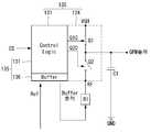
도 10에 도시된 바와 같이, 본 발명의 제2실시예에 따른 게이트 펄스 변조부(135)는 로직 회로부(131), 스위치 회로부(134) 및 버퍼 회로부(136)를 포함한다.10, the
로직 회로부(131)는 타이밍 제어부로부터 출력된 제어신호(CS)와 비교 회로부(132)로부터 출력된 비교 결과에 대응하여 스위치 회로부(134)를 제어하는 스위치 제어신호(Q1C, Q2C)를 출력한다.The
버퍼 회로부(136)는 참조전압(Ref)을 버퍼링하고 게이트 펄스 변조부(135)의 입출력단자(RE)에 버퍼링된 참조전압(Ref)을 공급한다. 버퍼 회로부(136)에 의해 버퍼링된 참조전압(Ref)은 저항기(R)의 타단을 통해 게이트 펄스 변조부(135)의 입출력단자(RE)에 공급된다. 버퍼 회로부(136)의 입력단자는 참조전압라인에 연결되고 출력단자는 저항기(R)의 타단에 연결된다.The
스위치 회로부(134)는 로직 회로부(131)로부터 출력된 스위치 제어신호(Q1C, Q2C)에 대응하여 게이트하이전압(VGH)을 그대로 출력하거나 게이트하이전압(VGH)의 폴링 에지를 가변하여 출력하기 위한 스위칭 동작을 한다.The
스위치 회로부(134)는 게이트 펄스 변조부(135)의 게이트하이전압단자(VGH)와 입출력단자(RE) 사이에 배치된 제1스위치(Q1)와 제2스위치(Q2)를 포함한다.The
제1스위치(Q1)는 게이트 펄스 변조부(135)의 게이트하이전압단자(VGH)에 제1전극이 연결되고 게이트 펄스 변조부(135)의 출력단자(GPM출력)에 제2전극이 연결되고 제어신호라인에 게이트전극이 연결된다.The first switch Q1 has a first electrode connected to the gate high voltage terminal VGH of the
제2스위치(Q2)는 게이트 펄스 변조부(135)의 입출력단자(RE)에 제1전극이 연결되고 게이트 펄스 변조부(135)의 출력단자(GPM출력)에 제2전극이 연결되고 제어신호라인에 게이트전극이 연결된다.The second switch Q2 has the first electrode connected to the input / output terminal RE of the
저항기(R1)는 게이트 펄스 변조부(135)의 입출력단자(RE)(제2스위치의 제1전극)에 타단이 연결되고 버퍼 회로부(136)의 출력단자(GPM출력)에 일단이 연결된다. 커패시터(C1)는 게이트 펄스 변조부(135)의 출력단자(GPM출력)에 일단이 연결되고 그라운드전압라인(GND)에 타단이 연결된다. 커패시터(C1)는 게이트 펄스 변조부(135)의 출력단자(GPM출력)를 통해 출력되는 전압을 일정시간 유지하는 역할을 한다.The other end of the resistor R1 is connected to the input / output terminal RE (the first electrode of the second switch) of the
제2실시예는 실험예에서 유발되는 문제점을 해소하기 위해 게이트 펄스 변조부(135) 내에서 노이즈 필터부와 비교 회로부를 제거한다. 대신, 버퍼 회로부(136)의 출력단을 통해 출력된 참조전압(Ref)이 저항기(R1)의 일단에 전달되도록 구성한다. 게이트 펄스 변조부(135) 내에 버퍼 회로부(136)를 추가하고 출력단자에 저항기(R1)의 일단을 연결하면, 참조전압(Ref)을 기반으로 방전을 유도할 수 있다.The second embodiment removes the noise filter portion and the comparison circuit portion in the
제2실시예에 따른 게이트 펄스 변조부(135)는 도 11a 및 도 11b의 순서로 동작한다. 게이트 펄스 변조부(135)의 동작에 따른 출력은 GPM 출력을 나타내는 도 12를 참조한다.The
도 11a 및 도 12에 도시된 바와 같이, 제1스위치(Q1)가 턴온되고 제2스위치(Q2)가 턴오프되면 게이트하이전압(VGH)은 그대로 출력된다. 즉, 게이트 펄스 변조부(135)는 게이트하이전압(VGH)의 폴링 에지를 변조하지 않고 그대로 출력한다. (도 12의 ① 구간 참조)As shown in Figs. 11A and 12, when the first switch Q1 is turned on and the second switch Q2 is turned off, the gate high voltage VGH is output as it is. That is, the
도 11b 및 도 12에 도시된 바와 같이, 제1스위치(Q1)가 턴오프되고 제2스위치(Q2)가 턴온되면 이전에 출력된 게이트하이전압(VGH)은 저항기(R1)를 통해 일정시간 동안 방전이 일어난다. 이때, 게이트 펄스 변조부(135)의 출력단자의 전압 레벨은 참조전압(Ref)과 동일한 전압(GPM출력 = Buffer출력 = Ref)이 형성된다. 이에 따라, 게이트하이전압(VGH)은 로직하이(H)에서 참조전압(Ref)과 등전위 레벨에 해당하는 로직로우(L)로 떨어지게 된다. (도 12의 ② 구간 참조)As shown in FIGS. 11B and 12, when the first switch Q1 is turned off and the second switch Q2 is turned on, the previously outputted gate high voltage VGH passes through the resistor R1 for a predetermined time Discharge occurs. At this time, the voltage level of the output terminal of the
제2실시예에 따른 게이트 펄스 변조부(135)는 참조전압(Ref)을 기반으로 게이트하이전압(VGH)을 가변하기 위한 방전이 수행되므로 도 6의 ③ 구간과 같은 신호 지연이 발생하지 않는다. 또한, 게이트 펄스 변조부(135)의 출력단자는 도 6의 ④ 구간과 같이 플로팅(floating) 상태가 되지 않고 참조전압(Ref)으로 유지 및 방전(플로팅에 의한 자연 방전 없음)된다.The
이상과 같은 구성에 의해, 제2실시예에 따른 게이트 펄스 변조부(135)는 회로의 구성 및 동작을 단순화하여 신호 지연 문제 등을 해소하고 전압 출력 이후 커패시터(C1)의 자연 방전으로 인한 전압 레벨의 하강이 유발되지 않도록 참조전압(Ref)과 등전위로 출력전압을 유지한다.With the above configuration, the
그 결과, 제2실시예에 따른 게이트 펄스 변조부(135)는 게이트하이전압(VGH)의 레벨 가변시 하강 정지 레벨(Falling Stop Level)의 정확성과 구동 정밀도를 향상할 수 있다. 또한, 제2실시예에 따른 게이트 펄스 변조부(135)를 갖는 전원 공급부(130)는 구동 정밀도를 높여 표시패널의 화면 양단의 어두움 또는 게이트 구동부들 간의 휘도차에 따른 게이트 블록 딤(Gate Block Dim) 등이 유발되는 문제를 해소 및 개선할 수 있다.As a result, the
한편, 버퍼 회로부(136)는 다음과 같이 구성될 수 있다.On the other hand, the
도 13 및 도 14는 버퍼 회로부의 구성 예시도들이며, 도 15 및 도 16은 버퍼 회로부의 구성에 따른 출력 파형도들이다.Figs. 13 and 14 are exemplary configurations of the buffer circuit section, and Figs. 15 and 16 are output waveform diagrams according to the configuration of the buffer circuit section.
도 10 및 도 13에 도시된 바와 같이, 버퍼 회로부(136)는 증폭기(AMP)로 구성될 수 있다. 증폭기(AMP)는 참조전압라인(Ref)에 제1단자(+)(비반전 입력단자)가 연결되고 출력단자(OUT)에 제2단자(-)(반전 입력단자)가 연결된다.As shown in Figs. 10 and 13, the
도 10 및 도 14에 도시된 바와 같이, 버퍼 회로부(136)는 증폭기(AMP), 제1가변저항기(RV1) 및 제2가변저항기(RV2)로 구성될 수 있다. 제1가변저항기(RV1) 및 제2가변저항기(RV2)는 타이밍 제어부(외부 회로) 또는 전원 공급부(내부 회로) 등의 레지스터값에 따라 저항값(또는 저항비율)이 가변된다.As shown in FIGS. 10 and 14, the
증폭기(AMP)는 참조전압라인(Ref)에 제1단자(+)(비반전단자)가 연결된다. 제1가변저항기(RV1)는 증폭기(AMP)의 제2단자(-)(반전단자)에 일단이 연결되고 증폭기(AMP)의 출력단자(OUT)에 타단이 연결된다. 제2가변저항기(RV2)는 증폭기(AMP)의 출력단자(OUT)에 일단이 연결되고 제1저항기(R1)의 일단에 타단이 연결된다.In the amplifier AMP, the first terminal (+) (non-inverting terminal) is connected to the reference voltage line Ref. The first variable resistor RV1 is connected at one end to the second terminal (-) (inverting terminal) of the amplifier AMP and at the other end to the output terminal OUT of the amplifier AMP. The second variable resistor RV2 has one end connected to the output terminal OUT of the amplifier AMP and the other end connected to one end of the first resistor R1.
제1가변저항기(RV1)와 제2가변저항기(RV2)의 저항비율은 1:1, 1:2, 1:3 등과 같이 어느 한쪽의 비율을 높일 수 있다. 제1가변저항기(RV1)와 제2가변저항기(RV2)의 저항비율을 이와 같이 설정하면, 도 15와 같이 게이트하이전압(VGH)의 방전 레벨을 가변할 수 있다.The ratio of the resistances of the first variable resistor RV1 and the second variable resistor RV2 may be 1: 1, 1: 2, 1: 3, or the like. When the resistance ratio between the first variable resistor RV1 and the second variable resistor RV2 is set as described above, the discharge level of the gate high voltage VGH can be varied as shown in FIG.
예컨대, 게이트하이전압(VGH)의 방전 레벨은 제1레벨(LV1) ~ 제3레벨(LV3) 등과 같이 참조전압보다 높아질 수 있다. 제1가변저항기(RV1)와 제2가변저항기(RV2)의 저항비율은 1:N(N은 2 이상 정수)으로 설정될 수 있다.For example, the discharge level of the gate high voltage VGH may be higher than the reference voltage, such as the first level LV1 to the third level LV3. The resistance ratio of the first variable resistor RV1 and the second variable resistor RV2 may be set to 1: N (N is an integer of 2 or more).
제1가변저항기(RV1)와 제2가변저항기(RV2)의 저항비율은 10:20, 20:40, 30:60 등과 같이 동일한 비율로 증가시킬 수 있다. 제1가변저항기(RV1)와 제2가변저항기(RV2)의 저항비율을 이와 같이 설정하면, 도 16과 같이 게이트하이전압(VGH)의 방전 기울기를 가변할 수 있다.The resistance ratio of the first variable resistor RV1 and the second variable resistor RV2 may be increased by the same ratio as 10:20, 20:40, 30:60, and so on. If the resistance ratio between the first variable resistor RV1 and the second variable resistor RV2 is set as described above, the discharge gradient of the gate high voltage VGH can be varied as shown in FIG.
예컨대, 게이트하이전압(VGH)의 방전 기울기는 제1기울기(A1) ~ 제3기울기(A3) 등과 같이 완만하거나 가파르게 형성될 수 있다. 제1가변저항기(RV1)와 제2가변저항기(RV2)의 저항비율은 M:N(M은 1 이상 정수, N은 2 이상 정수이며, M < N)으로 설정될 수 있다.For example, the discharge slope of the gate high voltage VGH may be formed gently or steeply, such as the first slope A1 to the third slope A3. The resistance ratio of the first variable resistor RV1 and the second variable resistor RV2 may be set to M: N (M is an integer of 1 or more, N is an integer of 2 or more, and M < N).
이상과 같이 게이트하이전압(VGH)의 방전 레벨과 방전 기울기를 가변하면 표시장치의 구동 특성에 맞게 게이트신호를 형성하면서도 전압 레벨의 가변을 통해 장치의 소비전력을 절감할 수 있게 된다.As described above, when the discharge level and the discharge gradient of the gate high voltage (VGH) are varied, the power consumption of the device can be reduced by varying the voltage level while forming the gate signal according to the driving characteristics of the display device.
이상 본 발명은 게이트 펄스 변조 회로의 구성 및 동작을 단순화함과 더불어 신호 지연 문제 등을 해소하여 전압 레벨 가변시 하강 정지 레벨(Falling Stop Level)의 정확성과 구동 정밀도를 향상할 수 있는 효과가 있다. 또한, 본 발명은 게이트 펄스 변조 회로의 구동 정밀도를 높여 표시패널의 화면 양단의 어두움 또는 게이트 구동부들 간의 휘도차에 따른 게이트 블록 딤(Gate Block Dim) 등이 유발되는 문제를 해소 및 개선할 수 있는 효과가 있다.The present invention simplifies the configuration and operation of the gate pulse modulation circuit, eliminates the signal delay problem, and improves the accuracy of the falling stop level and the driving precision when the voltage level is varied. In addition, the present invention can improve the driving precision of the gate pulse modulation circuit and solve or improve the problem of darkness at both ends of the screen of the display panel or gate block dim due to the luminance difference between the gate drivers It is effective.
이상 첨부된 도면을 참조하여 본 발명의 실시예를 설명하였지만, 상술한 본 발명의 기술적 구성은 본 발명이 속하는 기술 분야의 당업자가 본 발명의 그 기술적 사상이나 필수적 특징을 변경하지 않고서 다른 구체적인 형태로 실시될 수 있다는 것을 이해할 수 있을 것이다. 그러므로 이상에서 기술한 실시 예들은 모든 면에서 예시적인 것이며 한정적인 것이 아닌 것으로서 이해되어야 한다. 아울러, 본 발명의 범위는 상기 상세한 설명보다는 후술하는 특허청구범위에 의하여 나타내어진다. 또한, 특허청구범위의 의미 및 범위 그리고 그 등가 개념으로부터 도출되는 모든 변경 또는 변형된 형태가 본 발명의 범위에 포함되는 것으로 해석되어야 한다.While the present invention has been described in connection with what is presently considered to be practical exemplary embodiments thereof, it is to be understood that the invention is not limited to the disclosed embodiments, but, on the contrary, It will be understood that the invention may be practiced. It is therefore to be understood that the embodiments described above are to be considered in all respects only as illustrative and not restrictive. In addition, the scope of the present invention is indicated by the following claims rather than the detailed description. Also, all changes or modifications derived from the meaning and scope of the claims and their equivalents should be construed as being included within the scope of the present invention.
100: 표시패널110: 타이밍 제어부
120: 데이터 구동부130: 전원 공급부
140A, 140B: 게이트 구동부135: 게이트 펄스 변조부
139: 게이트 전압 출력부VGH: 게이트하이전압
131: 로직 회로부134: 스위치 회로부
136: 버퍼 회로부R1: 저항기
Ref: 의참조전압RV1: 제1가변저항기
RV2: 제2가변저항기100: display panel 110: timing controller
120: Data driver 130: Power supply
140A, 140B: Gate driver 135: Gate pulse modulation unit
139: Gate voltage output part VGH: Gate high voltage
131: logic circuit part 134: switch circuit part
136: Buffer circuit section R1: Resistor
Ref: reference voltage of RV1: first variable resistor
RV2: second variable resistor
Claims (10)
Translated fromKorean외부로부터 공급된 제어신호에 대응하여 상기 스위치 회로부를 제어하기 위한 스위치 제어신호를 출력하는 로직 회로부를 포함하고,
상기 스위치 회로부는 자신의 출력단자를 통해 출력된 상기 게이트 전압의 폴링 에지를 참조전압으로 방전시키는 게이트 펄스 변조 회로.A switch circuit for performing a switching operation for outputting the gate voltage as it is or changing its output terminal through its own output terminal; And
And a logic circuit unit for outputting a switch control signal for controlling the switch circuit unit in response to a control signal supplied from the outside,
Wherein the switch circuit part discharges the falling edge of the gate voltage output through its output terminal to a reference voltage.
상기 참조전압을 상기 스위치 회로부에 전달하는 저항기를 포함하는 게이트 펄스 변조 회로.The method according to claim 1,
And a resistor for transmitting the reference voltage to the switch circuit.
상기 참조전압을 버퍼링하여 상기 저항기에 전달하는 버퍼 회로부를 포함하는 게이트 펄스 변조 회로.3. The method of claim 2,
And a buffer circuit for buffering the reference voltage and transmitting the buffered voltage to the resistor.
상기 버퍼 회로부는
상기 참조전압을 전달하는 참조전압라인에 입력단자가 연결되고 상기 저항기의 일단에 출력단자가 연결된 게이트 펄스 변조 회로.The method of claim 3,
The buffer circuit section
A gate pulse modulation circuit in which an input terminal is connected to a reference voltage line for transmitting the reference voltage and an output terminal is connected to one end of the resistor.
상기 버퍼 회로부는
외부 또는 내부 레지스터값에 따라 상기 게이트 전압의 방전 레벨과 방전 기울기를 가변하는 가변저항기들을 포함하는 게이트 펄스 변조 회로.5. The method of claim 4,
The buffer circuit section
And variable resistors varying a discharge level and a discharge slope of the gate voltage according to an external or internal register value.
상기 버퍼 회로부는
외부 또는 내부 레지스터값에 따라 저항값이 가변되는 제1가변저항기와 제2가변저항기를 포함하고,
상기 제1가변저항기는 상기 버퍼 회로부의 반전단자에 일단이 연결되고 상기 버퍼 회로부의 출력단자에 타단이 연결되며,
상기 제2가변저항기는 상기 버퍼 회로부의 출력단자에 일단이 연결되고 상기 저항기의 일단에 타단이 연결된 게이트 펄스 변조 회로.5. The method of claim 4,
The buffer circuit section
A first variable resistor and a second variable resistor whose resistance values vary according to an external or internal register value,
The first variable resistor may have one end connected to the inverting terminal of the buffer circuit part and the other end connected to the output terminal of the buffer circuit part,
And the second variable resistor has one end connected to the output terminal of the buffer circuit portion and the other end connected to one end of the resistor.
상기 제1가변저항기와 상기 제2가변저항기의 저항비율은
M:N(M은 1 이상 정수, N은 2 이상 정수이며, M < N)인 게이트 펄스 변조 회로.The method according to claim 6,
The resistance ratio of the first variable resistor and the second variable resistor is
M: N (where M is an integer equal to or greater than 1, and N is an integer equal to or greater than 2, and M < N).
게이트 전압을 그대로 또는 가변하여 출력하는 게이트 펄스 변조 회로를 포함하는 전원 공급부; 및
상기 전원 공급부로부터 출력된 상기 게이트 전압을 기반으로 상기 표시패널에 공급할 게이트신호를 마련하는 게이트 구동부를 포함하고,
상기 게이트 펄스 변조 회로는
상기 게이트 전압을 그대로 또는 가변하여 자신의 출력단자를 통해 출력하기 위한 스위칭 동작을 수행하는 스위치 회로부와, 외부로부터 공급된 제어신호에 대응하여 상기 스위치 회로부를 제어하기 위한 스위치 제어신호를 출력하는 로직 회로부를 포함하고,
상기 스위치 회로부는 자신의 출력단자를 통해 출력된 상기 게이트 전압의 폴링 에지를 참조전압으로 방전시키는 표시장치.A display panel for displaying an image;
A power supply unit including a gate pulse modulation circuit for outputting the gate voltage as it is or changing it; And
And a gate driver for providing a gate signal to be supplied to the display panel based on the gate voltage output from the power supply unit,
The gate pulse modulation circuit
A switch circuit section for performing a switching operation for directly or varying the gate voltage and outputting the gate voltage through its own output terminal and a logic circuit section for outputting a switch control signal for controlling the switch circuit section in response to a control signal supplied from the outside, Lt; / RTI >
Wherein the switch circuit part discharges the falling edge of the gate voltage output through its output terminal to a reference voltage.
상기 참조전압을 상기 스위치 회로부에 전달하는 저항기와,
상기 참조전압을 버퍼링하여 상기 저항기에 전달하는 버퍼 회로부를 포함하는 표시장치.9. The method of claim 8,
A resistor for transmitting the reference voltage to the switch circuit,
And a buffer circuit for buffering the reference voltage and transmitting the buffered voltage to the resistor.
상기 버퍼 회로부는
외부 또는 내부 레지스터값에 따라 저항값이 가변되는 제1가변저항기와 제2가변저항기를 포함하고,
상기 제1가변저항기는 상기 버퍼 회로부의 반전단자에 일단이 연결되고 상기 버퍼 회로부의 출력단자에 타단이 연결되며,
상기 제2가변저항기는 상기 버퍼 회로부의 출력단자에 일단이 연결되고 상기 저항기의 일단에 타단이 연결된 표시장치.10. The method of claim 9,
The buffer circuit section
A first variable resistor and a second variable resistor whose resistance values vary according to an external or internal register value,
The first variable resistor may have one end connected to the inverting terminal of the buffer circuit part and the other end connected to the output terminal of the buffer circuit part,
And the second variable resistor has one end connected to the output terminal of the buffer circuit portion and the other end connected to one end of the resistor.
Priority Applications (1)
| Application Number | Priority Date | Filing Date | Title |
|---|---|---|---|
| KR1020150191819AKR102461390B1 (en) | 2015-12-31 | 2015-12-31 | Gate Pulse Modulation Circuit and Display Device Using the same |
Applications Claiming Priority (1)
| Application Number | Priority Date | Filing Date | Title |
|---|---|---|---|
| KR1020150191819AKR102461390B1 (en) | 2015-12-31 | 2015-12-31 | Gate Pulse Modulation Circuit and Display Device Using the same |
Publications (2)
| Publication Number | Publication Date |
|---|---|
| KR20170080350Atrue KR20170080350A (en) | 2017-07-10 |
| KR102461390B1 KR102461390B1 (en) | 2022-10-31 |
Family
ID=59355635
Family Applications (1)
| Application Number | Title | Priority Date | Filing Date |
|---|---|---|---|
| KR1020150191819AActiveKR102461390B1 (en) | 2015-12-31 | 2015-12-31 | Gate Pulse Modulation Circuit and Display Device Using the same |
Country Status (1)
| Country | Link |
|---|---|
| KR (1) | KR102461390B1 (en) |
Cited By (2)
| Publication number | Priority date | Publication date | Assignee | Title |
|---|---|---|---|---|
| US11538415B2 (en) | 2018-08-03 | 2022-12-27 | Samsung Display Co., Ltd. | Clock and voltage generation circuit and display device including the same |
| US11978420B2 (en) | 2021-12-07 | 2024-05-07 | Lx Semicon Co., Ltd. | Gate driving device for driving display panel |
Citations (3)
| Publication number | Priority date | Publication date | Assignee | Title |
|---|---|---|---|---|
| KR20070078164A (en)* | 2006-01-26 | 2007-07-31 | 삼성전자주식회사 | Drive device for display device and display device including same |
| KR20140030722A (en)* | 2012-09-03 | 2014-03-12 | 삼성디스플레이 주식회사 | Driving device of display device |
| KR20140041046A (en)* | 2012-09-27 | 2014-04-04 | 엘지디스플레이 주식회사 | Organic light emitting display and method of modulating gate signal voltage thereof |
- 2015
- 2015-12-31KRKR1020150191819Apatent/KR102461390B1/enactiveActive
Patent Citations (3)
| Publication number | Priority date | Publication date | Assignee | Title |
|---|---|---|---|---|
| KR20070078164A (en)* | 2006-01-26 | 2007-07-31 | 삼성전자주식회사 | Drive device for display device and display device including same |
| KR20140030722A (en)* | 2012-09-03 | 2014-03-12 | 삼성디스플레이 주식회사 | Driving device of display device |
| KR20140041046A (en)* | 2012-09-27 | 2014-04-04 | 엘지디스플레이 주식회사 | Organic light emitting display and method of modulating gate signal voltage thereof |
Cited By (2)
| Publication number | Priority date | Publication date | Assignee | Title |
|---|---|---|---|---|
| US11538415B2 (en) | 2018-08-03 | 2022-12-27 | Samsung Display Co., Ltd. | Clock and voltage generation circuit and display device including the same |
| US11978420B2 (en) | 2021-12-07 | 2024-05-07 | Lx Semicon Co., Ltd. | Gate driving device for driving display panel |
Also Published As
| Publication number | Publication date |
|---|---|
| KR102461390B1 (en) | 2022-10-31 |
Similar Documents
| Publication | Publication Date | Title |
|---|---|---|
| KR102472193B1 (en) | Data drivign circuit, display panel and display device | |
| JP4758332B2 (en) | Liquid crystal display | |
| EP1811488B1 (en) | Driving device and display device using the same | |
| CN111179798A (en) | Display device and driving method thereof | |
| KR101209043B1 (en) | Driving apparatus for display device and display device including the same | |
| KR20180036893A (en) | Gate driving circuit and display device using the same | |
| KR20080060077A (en) | LCD and its quality improvement method | |
| US20120120044A1 (en) | Liquid crystal display device and method for driving the same | |
| KR20180066375A (en) | Shift Register and Display Device Using the same | |
| KR20160033351A (en) | Display device | |
| KR20110062608A (en) | LCD Display | |
| CN116110334A (en) | Display device and data driving circuit | |
| KR20170028000A (en) | Display device and driving method of the same | |
| CN102376284B (en) | Electro-optical device and electronic equipment | |
| KR102420492B1 (en) | Level shifter device using serial interface and display device having the same | |
| US8913046B2 (en) | Liquid crystal display and driving method thereof | |
| KR20160035154A (en) | Liquid crystal display device and driving method thereof | |
| KR101969411B1 (en) | Liquid crystal display device and clock pulse generation circuit thereof | |
| KR101244773B1 (en) | Display device | |
| KR20230101617A (en) | Gate Driving Circuit and Display Device using the same | |
| KR102461390B1 (en) | Gate Pulse Modulation Circuit and Display Device Using the same | |
| KR102461388B1 (en) | Scan Driver and Display Device Using the same | |
| CN118248061A (en) | Level converter and display device using the same | |
| KR102481897B1 (en) | Display device and the method for driving the same | |
| CN107799046A (en) | Display device and controller |
Legal Events
| Date | Code | Title | Description |
|---|---|---|---|
| PA0109 | Patent application | St.27 status event code:A-0-1-A10-A12-nap-PA0109 | |
| PG1501 | Laying open of application | St.27 status event code:A-1-1-Q10-Q12-nap-PG1501 | |
| P22-X000 | Classification modified | St.27 status event code:A-2-2-P10-P22-nap-X000 | |
| R17-X000 | Change to representative recorded | St.27 status event code:A-3-3-R10-R17-oth-X000 | |
| A201 | Request for examination | ||
| PA0201 | Request for examination | St.27 status event code:A-1-2-D10-D11-exm-PA0201 | |
| R17-X000 | Change to representative recorded | St.27 status event code:A-3-3-R10-R17-oth-X000 | |
| E902 | Notification of reason for refusal | ||
| PE0902 | Notice of grounds for rejection | St.27 status event code:A-1-2-D10-D21-exm-PE0902 | |
| E13-X000 | Pre-grant limitation requested | St.27 status event code:A-2-3-E10-E13-lim-X000 | |
| P11-X000 | Amendment of application requested | St.27 status event code:A-2-2-P10-P11-nap-X000 | |
| P13-X000 | Application amended | St.27 status event code:A-2-2-P10-P13-nap-X000 | |
| E90F | Notification of reason for final refusal | ||
| PE0902 | Notice of grounds for rejection | St.27 status event code:A-1-2-D10-D21-exm-PE0902 | |
| P11-X000 | Amendment of application requested | St.27 status event code:A-2-2-P10-P11-nap-X000 | |
| P13-X000 | Application amended | St.27 status event code:A-2-2-P10-P13-nap-X000 | |
| E701 | Decision to grant or registration of patent right | ||
| PE0701 | Decision of registration | St.27 status event code:A-1-2-D10-D22-exm-PE0701 | |
| GRNT | Written decision to grant | ||
| PR0701 | Registration of establishment | St.27 status event code:A-2-4-F10-F11-exm-PR0701 | |
| PR1002 | Payment of registration fee | St.27 status event code:A-2-2-U10-U11-oth-PR1002 Fee payment year number:1 | |
| PG1601 | Publication of registration | St.27 status event code:A-4-4-Q10-Q13-nap-PG1601 | |
| PR1001 | Payment of annual fee | St.27 status event code:A-4-4-U10-U11-oth-PR1001 Fee payment year number:4 |