KR20170080217A - Touch display device and driving method thereof - Google Patents
Touch display device and driving method thereofDownload PDFInfo
- Publication number
- KR20170080217A KR20170080217AKR1020150191522AKR20150191522AKR20170080217AKR 20170080217 AKR20170080217 AKR 20170080217AKR 1020150191522 AKR1020150191522 AKR 1020150191522AKR 20150191522 AKR20150191522 AKR 20150191522AKR 20170080217 AKR20170080217 AKR 20170080217A
- Authority
- KR
- South Korea
- Prior art keywords
- touch
- common voltage
- block
- blocks
- display panel
- Prior art date
- Legal status (The legal status is an assumption and is not a legal conclusion. Google has not performed a legal analysis and makes no representation as to the accuracy of the status listed.)
- Granted
Links
Images


Classifications
- G—PHYSICS
- G06—COMPUTING OR CALCULATING; COUNTING
- G06F—ELECTRIC DIGITAL DATA PROCESSING
- G06F3/00—Input arrangements for transferring data to be processed into a form capable of being handled by the computer; Output arrangements for transferring data from processing unit to output unit, e.g. interface arrangements
- G06F3/01—Input arrangements or combined input and output arrangements for interaction between user and computer
- G06F3/03—Arrangements for converting the position or the displacement of a member into a coded form
- G06F3/041—Digitisers, e.g. for touch screens or touch pads, characterised by the transducing means
- G06F3/0412—Digitisers structurally integrated in a display
- G—PHYSICS
- G06—COMPUTING OR CALCULATING; COUNTING
- G06F—ELECTRIC DIGITAL DATA PROCESSING
- G06F3/00—Input arrangements for transferring data to be processed into a form capable of being handled by the computer; Output arrangements for transferring data from processing unit to output unit, e.g. interface arrangements
- G06F3/01—Input arrangements or combined input and output arrangements for interaction between user and computer
- G06F3/03—Arrangements for converting the position or the displacement of a member into a coded form
- G06F3/041—Digitisers, e.g. for touch screens or touch pads, characterised by the transducing means
- G06F3/0416—Control or interface arrangements specially adapted for digitisers
Landscapes
- Engineering & Computer Science (AREA)
- General Engineering & Computer Science (AREA)
- Theoretical Computer Science (AREA)
- Human Computer Interaction (AREA)
- Physics & Mathematics (AREA)
- General Physics & Mathematics (AREA)
- Liquid Crystal Display Device Control (AREA)
- Control Of Indicators Other Than Cathode Ray Tubes (AREA)
Abstract
Translated fromKoreanDescription
Translated fromKorean본 발명은 터치표시장치에 관한 것으로, 특히 화소전압의 충전시간을 확보하여 동작 신뢰성을 향상시킬 수 있는 인셀 구조의 터치표시장치 및 이의 동작방법에 관한 것이다.BACKGROUND OF THE
터치표시장치는 액정표시장치, 전계방출표시장치, 플라즈마 디스플레이패널, 유기발광표시장치 등과 같은 화상표시장치에 터치패널을 설치하고, 사용자에 의해 터치패널이 가압되어 미리 정해진 정보가 출력되는 표시장치이다.A touch display device is a display device in which a touch panel is installed in an image display device such as a liquid crystal display device, a field emission display device, a plasma display panel, an organic light emitting display device, etc., and the touch panel is pressed by a user to output predetermined information .
최근, 스마트폰, 태블릿 PC 등과 같은 휴대용 단말기의 슬림화를 위해 표시장치의 내부에 터치패널을 구성하는 소자들을 내장하는 인셀(In-cell) 구조의 터치표시장치에 대한 수요가 증가하고 있다.2. Description of the Related Art In recent years, in order to reduce the size of portable terminals such as smart phones, tablet PCs, and the like, there has been an increasing demand for an in-cell touch display device that incorporates elements constituting a touch panel in a display device.
인셀 구조의 터치표시장치는 통상의 표시장치에 구비되는 게이트라인 및 데이터라인 이외에, 추가적으로 터치를 감지하는 다수의 터치블록 및 이에 연결된 센싱라인이 구비된다.The touch display device of an inshell structure includes a plurality of touch blocks for sensing touch and a sensing line connected thereto in addition to gate lines and data lines provided in a normal display device.
도 1은 일반적인 인셀 구조의 터치표시장치를 나타내는 도면이다.FIG. 1 is a view showing a general touch display device of an inshell structure.
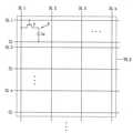
도 1에 도시된 바와 같이, 인셀 구조의 터치표시장치는 터치표시패널(10) 상에 다수의 화소(미도시)를 정의하는 게이트신호라인(GL) 및 데이터신호라인(DL)이 교차되어 형성되고, 각 화소에 공통전압(VCOM)을 인가하는 공통전압라인(CL)이 형성된다. 또한, 터치표시패널(10)에는 터치가 발생된 위치를 감지하여 구동유닛(20)으로 출력하는 센싱라인(미도시)이 형성되며, 센싱라인은 x축 방향으로 연장된 x축 센싱라인(미도시)과 y축 방향으로 연장된 y축 센싱라인(미도시)으로 구성된다. 터치표시패널(10)의 일측으로는 각 라인과 전기적으로 연결되는 구동유닛(20)이 실장된다.1, the touch display device of an in-cell structure includes a gate signal line GL and a data signal line DL that define a plurality of pixels (not shown) on a
터치표시패널(10)의 표시영역(A/A) 전체에 걸쳐 다수의 터치블록(TB_0~TB_N)이 구성된다. 다수의 터치블록(TB_0~TB_N) 각각은 공통전극(미도시)으로 구성되는 다수의 터치전극(미도시)을 구비한다. 각 터치블록(TB_0~TB_N)은 사용자의 터치 동작에 따른 화소전극(미도시)과 공통전극 간의 커패시턴스 변화를 센싱라인을 통해 구동유닛(20)으로 출력한다. 각 터치블록(TB_0~TB_N)은 다수의 게이트신호라인(GL)에 해당되는 영역과 대응된다.A plurality of touch blocks TB_0 to TB_N are formed over the entire display area A / A of the
상술한 터치표시장치는, 사용자로부터 터치표시패널(10)에 대한 터치가 발생되면, 화소전극 및 터치전극, 즉 공통전극에 의해 발생되는 커패시턴스 변화에 따라 구동유닛(20)이 사용자의 터치 위치를 인식하게 된다. 이를 위하여, 공통전극에는 화소전압에 대응되는 직류파형 및 터치 인식을 위한 센싱파형이 교번적으로 나타나는 공통전압(VCOM)이 인가된다.When the user touches the touch-
이때, 센싱파형의 공통전압(VCOM)과 직류파형의 공통전압(VCOM)이 동시에 인가되면, 화소전극과 공통전극의 전압이 동시에 변화되어 정상적인 터치 인식이 불가능하므로, 터치표시장치는 하나의 수평기간(1H) 동안 직류파형의 공통전압(VCOM)과 센싱파형이 공통전압(VCOM)을 시분할하여 인가한다. 이에 따라, 터치표시장치는 디스플레이구간 및 터치감지구간으로 시분할 구동된다.At this time, if the common voltage VCOM of the sensing waveform and the common voltage VCOM of the DC waveform are simultaneously applied, the voltages of the pixel electrode and the common electrode are simultaneously changed and normal touch recognition is impossible. The common voltage VCOM of the DC waveform and the sensing waveform form the common voltage VCOM during the 1H period. Accordingly, the touch display device is time-division driven by the display section and the touch sensing section.
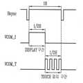
도 2는 인셀 구조의 터치표시장치의 구동에 따른 파형도이다.Fig. 2 is a waveform diagram according to driving of the touch display device of an in-cell structure.
도 2를 참조하면, 터치표시장치는 수평동기신호(Hsync)에 의해 정의되는 1수평기간(1H) 동안 디스플레이구간(display period) 및 터치감지구간(touch sensing period)으로 시분할되어 구동된다.Referring to FIG. 2, the touch display device is time-divided and driven during a display period and a touch sensing period for one horizontal period (1H) defined by a horizontal synchronization signal Hsync.
즉, 터치표시패널(10)에서는 1수평기간(1H) 중, 선 순위로 고전위의 게이트신호를 하나의 터치블록(TB_0)의 게이트신호라인(GL)에 인가함과 동시에, 직류파형의 공통전압(VCOM_I)이 공통전압라인(CL)에 인가된다. 이어, 1수평기간(1H) 중, 후 순위로 하나의 터치블록(TB_0)의 공통전압라인(CL)에 일정 주기로 스윙하는 센싱파형의 공통전압(VCOM_T)이 인가된다. 이에 따라, 고전위의 게이트신호와 센싱파형의 공통전압(VCOM)_T이 중첩되지 않도록 한다.That is, in the
그러나, 기존의 터치표시장치는 한정된 폭을 갖는 1수평기간(1H)을 예를 들어 각 1/2씩 분할하여 직류파형의 공통전압(VCOM_I)과 센싱파형의 공통전압(VCOM_T)을 각 터치블록(TB)에 인가하는 경우, 각 공통전압이 인가되는 기간은 1/2수평기간(1/2H)으로 줄어들게 된다.However, in the conventional touch display device, one horizontal period (1H) having a limited width is divided by, for example, 1/2, so that the common voltage VCOM_I of the DC waveform and the common voltage VCOM_T of the sensing waveform are supplied to the respective touch blocks (TB), the period in which each common voltage is applied is reduced to 1/2 horizontal period (1 / 2H).
따라서, 터치표시패널(10)에서 화소전극에 충전되는 화소전압의 충전시간이 감소되며, 이로 인해 크로스토크(cross-talk) 등과 같은 화질불량이 발생된다. 또한, 사용자의 터치감지를 위한 감지시간이 감소되며, 이로 인해 터치감도가 저하된다.Therefore, the charging time of the pixel voltage charged in the pixel electrode in the
특히, 터치표시장치가 오토모티브(automotive) 환경에서 사용되는 경우에, 저온 또는 고온에서 디스플레이 및 터치감지가 이루어지며, 상술한 화소전압의 충전시간 확보의 어려움 및 터치감도 저하에 의해 터치표시장치의 동작 신뢰성이 저하된다.Particularly, when the touch display device is used in an automotive environment, display and touch detection are performed at a low temperature or a high temperature, and the difficulty in securing the charging time of the pixel voltage and the deterioration of the touch sensitivity Reliability is lowered.
본 발명은 화소전압의 충전시간을 충분히 확보하고 터치감도를 향상시킬 수 있는 터치표시장치 및 이의 동작방법을 제공하는 데 있다.SUMMARY OF THE INVENTION It is an object of the present invention to provide a touch display device and a method of operating the touch display device capable of sufficiently securing the charging time of the pixel voltage and improving the touch sensitivity.
상기 목적을 달성하기 위한 본 발명의 터치표시장치는, 게이트구동부 및 전압생성부에 의해 다수의 터치블록이 공간분할 방식으로 동작되는 터치표시패널을 포함한다.According to an aspect of the present invention, there is provided a touch display apparatus including a touch display panel in which a plurality of touch blocks are operated in a space division manner by a gate driver and a voltage generator.
터치표시패널은 각각에 다수의 게이트신호라인 및 다수의 공통전압라인이 구비된 N(N은 자연수)개의 터치블록을 포함한다.The touch display panel includes N (N is a natural number) touch blocks each having a plurality of gate signal lines and a plurality of common voltage lines.
게이트구동부는 터치표시패널의 N개의 터치블록 중 제1터치블록의 다수의 게이트신호라인에 게이트신호를 인가한다.The gate driver applies a gate signal to a plurality of gate signal lines of the first touch block among the N touch blocks of the touch display panel.
전압생성부는 제1터치블록의 상기 다수의 공통전압라인에 제1공통전압을 인가하고, 동시에 N개의 터치블록 중 제N터치블록의 다수의 공통전압라인에 제2공통전압을 인가한다.The voltage generating unit applies a first common voltage to the plurality of common voltage lines of the first touch block and simultaneously applies a second common voltage to a plurality of common voltage lines of the Nth touch block among the N touch blocks.
상기 목적을 달성하기 위한 본 발명의 터치표시장치의 동작방법은, 터치표시패널의 다수의 터치블록 중 두 개의 터치블록을 동시에 디스플레이구간 및 터치감지구간으로 각각 할당하여 동작시키는 단계를 포함한다.According to another aspect of the present invention, there is provided a method of operating a touch display device including the steps of simultaneously assigning two touch blocks of a plurality of touch blocks of a touch display panel to a display section and a touch sensing section, respectively.
이때, 터치표시패널의 N개의 터치블록은 제1터치블록에서 제N터치블록의 순서대로 게이트신호 및 제1공통전압을 순차적으로 인가되어 디스플레이구간으로 할당되어 동작된다.At this time, the N touch blocks of the touch display panel are sequentially applied with the gate signal and the first common voltage sequentially from the first touch block to the Nth touch block, and are allocated to the display period and operated.
이와 동시에, 터치표시패널의 N개의 터치블록은 제N터치블록에서 제1터치블록의 순서대로 제2공통전압이 순차적으로 인가되어 터치감지구간으로 할당되어 동작된다.At the same time, the N touch blocks of the touch display panel are sequentially applied with the second common voltage in the order of the N-th touch block and the first touch block, and are allocated to the touch sensing interval and operated.
본 발명에 따른 터치표시장치는, 터치표시패널의 다수의 터치블록을 공간분할 방식으로 동작시켜 영상의 디스플레이와 사용자의 터치감지가 함께 수행되도록 함으로써, 화소전압의 충전시간을 충분하게 확보하면서 터치감도를 향상시킬 수 있다. 이로 인해, 오토모티브 환경에서 터치표시장치의 동작 신뢰성을 개선할 수 있다.The touch display device according to the present invention operates a plurality of touch blocks of the touch display panel in a space division manner so that the display of the image and the touch detection of the user are performed together to secure sufficient charge time of the pixel voltage, Can be improved. This makes it possible to improve the operational reliability of the touch display device in an automotive environment.
도 1은 일반적인 인셀 구조의 터치표시장치를 나타내는 도면이다.
도 2는 인셀 구조의 터치표시장치의 구동에 따른 파형도이다.
도 3 및 도 4는 본 발명에 따른 터치표시장치의 구성을 나타내는 도면들이다.
도 5는 도 4의 터치표시패널의 일부분에 대한 구조를 나타낸 도면이다.
도 6은 본 발명의 터치표시장치의 동작에 따른 공통전압의 파형도이다.
도 7은 본 발명의 터치표시장치의 구간중첩 회피동작에 따른 터치블록의 신호파형에 대한 파형도이다.FIG. 1 is a view showing a general touch display device of an inshell structure.
Fig. 2 is a waveform diagram according to driving of the touch display device of an in-cell structure.
3 and 4 are views showing a configuration of a touch display device according to the present invention.
5 is a view showing a structure of a part of the touch display panel of Fig.
6 is a waveform diagram of a common voltage according to the operation of the touch display device of the present invention.
7 is a waveform diagram of a signal waveform of a touch block according to an overlap avoiding operation of the touch display device of the present invention.
이하, 첨부한 도면을 참조하여 본 발명에 따른 터치표시장치 및 이의 동작방법에 대해 상세히 설명한다.Hereinafter, a touch display apparatus and an operation method thereof according to the present invention will be described in detail with reference to the accompanying drawings.
도 3 및 도 4는 본 발명에 따른 터치표시장치의 구성을 나타내는 도면들이다. 도 5는 도 4의 터치표시패널의 일부분에 대한 구조를 나타낸 도면이다.3 and 4 are views showing a configuration of a touch display device according to the present invention. 5 is a view showing a structure of a part of the touch display panel of Fig.
도 3 내지 도 5를 참조하면, 본 발명의 터치표시장치(100)는 터치표시패널(101) 및 이를 구동하는 다수의 구동회로(102)를 포함할 수 있다.3 to 5, the
터치표시패널(101)은 터치패널(미도시)이 내장된 액정패널일 수 있다. 터치표시패널(101)은 다수의 게이트신호라인(GL) 및 다수의 데이터신호라인(DL)이 교차되고, 교차지점마다 박막트랜지스터(T) 및 액정셀(Lc)을 포함하는 화소(P)가 형성된다.The
각 화소(P)의 박막트랜지스터(T)는 게이트전극이 게이트신호라인(GL)에 연결되고, 소스전극이 데이터신호라인(DL)에 연결되며, 드레인전극이 액정셀(Lc)의 일단에 연결된다. 액정셀(Lc)은 일단이 박막트랜지스터(T)의 드레인전극에 연결되고, 타단이 공통전압라인(CL)에 연결된다.The thin film transistor T of each pixel P has a gate electrode connected to the gate signal line GL, a source electrode connected to the data signal line DL and a drain electrode connected to one end of the liquid crystal cell Lc do. The liquid crystal cell Lc has one end connected to the drain electrode of the thin film transistor T and the other end connected to the common voltage line CL.
박막트랜지스터(T)는 게이트신호라인(GL)을 통해 인가되는 고전위의 게이트신호에 의해 턴-온되고, 데이터신호라인(DL)을 통해 인가되는 화소전압을 액정셀(Lc)에 전달한다. 액정셀(Lc)은 전달된 화소전압을 충전하며, 충전된 화소전압을 다음 프레임까지 유지시킨다. 이때, 액정셀(Lc)의 타단에는 공통전압라인(CL)을 통해 공통전압, 예컨대 제1공통전압(VCOM_I)이 인가된다. 이에 따라, 각 화소(P)는 액정셀(Lc)에 충전된 화소전압과 공통전압라인(CL)을 통해 인가된 제1공통전압(VCOM_I)이 이루는 전계에 따라 액정의 배열 상태를 변화시켜 광 투과율을 조절함으로써, 화상을 표시하게 된다.The thin film transistor T is turned on by a high-potential gate signal applied through the gate signal line GL and transmits a pixel voltage applied through the data signal line DL to the liquid crystal cell Lc. The liquid crystal cell Lc charges the transmitted pixel voltage and maintains the charged pixel voltage until the next frame. At this time, a common voltage, for example, the first common voltage VCOM_I is applied to the other end of the liquid crystal cell Lc through the common voltage line CL. Accordingly, each pixel P changes the arrangement state of the liquid crystal according to the electric field formed by the pixel voltage charged in the liquid crystal cell Lc and the first common voltage VCOM_I applied through the common voltage line CL, By controlling the transmittance, an image is displayed.
터치표시패널(101)의 하나의 화소(P)는 게이트신호라인(GL) 및 공통전압라인(CL)에 의해 동일 수평라인에 속하는 다른 화소(P)와 연결될 수 있다. 또한, 하나의 화소(P)는 데이터신호라인(DL)에 의해 동일 수직라인에 속하는 다른 화소(P)와 연결될 수 있다.One pixel P of the
또한, 터치표시패널(101)에는 게이트신호라인(GL) 및 데이터신호라인(DL)이 형성된 층과 다른 층에 다수의 센싱라인(SL)이 형성될 수 있다. 다수의 센싱라인(SL)은 터치가 발생된 위치를 터치검출부(140)로 전달한다. 다수의 센싱라인(SL)은 x축 센싱라인 또는 y축 센싱라인을 포함할 수 있다.The
터치표시패널(101)의 표시영역 전체에는 다수의 터치블록(TB)이 구성될 수 있다. 다수의 터치블록(TB) 각각에는 다수의 터치전극, 예컨대 공통전극으로 구성된 다수의 터치전극이 배치될 수 있다. 다수의 터치블록(TB) 각각은 사용자의 터치 동작에 따라 발생되는 커패시턴스 변화를 센싱라인(SL)을 통해 터치검출부(140)로 출력한다.A plurality of touch blocks TB may be formed on the entire display region of the
다수의 터치블록(TB) 각각은 대략 40개의 수평라인, 즉 40개의 게이트신호라인(GL)에 해당하는 영역을 차지할 수 있다. 예컨대, 도 5에 도시된 바와 같이, 제1터치블록(TB_0)은 제1 내지 제40게이트신호라인(GL) 및 이에 연결된 화소(P)를 포함할 수 있다. 또한, 다수의 터치블록(TB)은 터치표시패널(101)의 표시영역에 대략 20개로 구성될 수 있다. 그러나, 상술한 본 실시예의 터치블록(TB)의 구성, 즉 내부에 포함되는 게이트신호라인의 수 및 총 개수는 제한되지 않는다.Each of the plurality of touch blocks TB may occupy an area corresponding to approximately 40 horizontal lines, that is, 40 gate signal lines GL. For example, as shown in FIG. 5, the first touch block TB_0 may include first to 40th gate signal lines GL and pixels P connected thereto. In addition, the number of the touch blocks TB may be approximately 20 in the display area of the
다수의 구동회로(102)는 타이밍제어부(110), 게이트구동부(120), 데이터구동부(130), 터치검출부(140) 및 전압생성부(150)를 포함할 수 있다.The plurality of
타이밍제어부(110)는 외부시스템(미도시)으로부터 제공된 타이밍신호(TS)에 따라 게이트제어신호(GCS), 데이터제어신호(DCS) 및 터치제어신호(TCS)를 생성할 수 있다. 타이밍신호(TS)는 수평동기신호(Hsync), 수직동기신호(Vsync), 데이터인에이블신호(DE) 및 클럭신호(DCLK) 등을 포함할 수 있다. 게이트제어신호(GCS)는 게이트구동부(120)로 출력되고, 데이터제어신호(DCS)는 데이터구동부(130)로 출력된다. 터치제어신호(TCS)는 터치검출부(140)로 출력된다.The
또한, 타이밍제어부(110)는 외부시스템에서 제공된 영상신호(RGB)를 터치표시패널(101)의 해상도에 따라 재정렬하여 영상데이터(DATA)를 생성할 수 있다. 영상데이터(DATA)는 데이터제어신호(DCS)와 함께 데이터구동부(130)로 출력된다.In addition, the
게이트구동부(120)는 타이밍제어부(110)로부터 제공된 게이트제어신호(GCS)에 따라 게이트신호를 생성할 수 있다. 게이트신호는 터치표시패널(101)의 다수의 게이트신호라인(GL)에 순차적으로 출력될 수 있다. 게이트구동부(120)는 다수의 게이트신호라인(GL)에 연결되는 다수의 쉬프트레지스터로 이루어질 수 있으며, 터치표시패널(101)에 씨오에프(Chip On Film; COF) 형태로 부착되거나 또는 터치표시패널(101) 내에 지아이피(Gate In Panel; GIP) 형태로 구성될 수 있다.The
여기서, 타이밍제어부(110)로부터 제공되는 게이트제어신호(GCS)는 게이트스타트펄스(GSP; Gate Start Pulse), 게이트쉬프트클럭(GSC; Gate Shift Clock), 게이트출력인에이블(GOE; Gate Output Enable) 등을 포함한다. 게이트스타트펄스(GSP)는 게이트구동부(120)의 동작 시작을 제어하는 신호이고, 게이트쉬프트클럭(GSC)은 게이트구동부(120)에 입력되는 클럭신호로, 게이트스타트펄스(GSP)를 쉬프트 시키는 신호이다. 게이트출력인에이블(GOE)은 게이트구동부(120)의 출력 타이밍을 제어하는 신호이다.The gate control signal GCS provided from the
데이터구동부(130)는 타이밍제어부(110)로부터 제공된 데이터제어신호(DCS)에 따라 영상데이터(DATA)를 화소전압으로 변환한다. 화소전압은 하나의 수평구간(1H)만큼 래치되어 모든 데이터신호라인(DL)을 통해 동시에 터치표시패널(101)로 출력된다.The
여기서, 타이밍제어부(110)로부터 제공되는 데이터제어신호(DCS)는 소스스타트펄스(SSP; Source Start Pulse), 소스쉬프트클럭(SSC; Source Shift Clock) 및 소스출력인에이블(SOE; Source Output Enable) 등을 포함한다. 소스스타트펄스(SSP)는 데이터구동부(130)의 데이터 샘플링 시작 타이밍을 제어하는 신호이고, 소스샘플링클럭(SSC)은 라이징 또는 폴링 에지에 대응하여 데이터구동부(130)를 구성하는 각 구동IC에서 데이터 샘플링 타이밍을 제어하는 클럭신호이다. 소스출력인에이블(SOE)은 데이터구동부(130)의 출력 타이밍을 제어하는 신호이다.The data control signal DCS provided from the
터치검출부(140)는 타이밍제어부(110)로부터 제공된 터치제어신호(TCS)에 따라 터치표시패널(101)에 대한 사용자의 터치 유무를 검출하고, 검출 결과에 따라 사용자의 터치 위치를 구할 수 있다. 터치검출부(140)는 LPF(Low Pass Filter, 미도시), A/D 컨버터(미도시), 신호처리부(미도시) 및 좌표추출부(미도시) 등을 포함할 수 있다. LPF는 터치표시패널(101)의 센싱라인(SL)을 통해 전달된 센싱 결과에서 고주파 성분을 제거하여 출력한다. A/D 컨버터는 LPF로부터 출력되는 신호를 디지털 데이터로 변환한다. 신호처리부는 변환된 디지털 데이터에 따라 터치표시패널(101)의 터치블록(TB)에 대한 터치 유무를 검출한다. 좌표추출부는 터치 검출결과에 따라 좌표를 추출한다. 여기서, 터치검출부는 데이터 구동부 또는 게이트 구동부 내에 형성될 수 있다.The
전압생성부(150)는 터치표시패널(101)의 공통전압라인(CL)을 통해 각 터치블록(TB)에 공급되는 공통전압(VCOM_I, VCOM_T)을 생성할 수 있다. 전압생성부(150)는 두 종류의 공통전압(VCOM_I, VCOM_T)을 생성할 수 있는데, 예컨대 고정된 전위를 갖는 직류파형의 제1공통전압(VCOM_I) 및 소정 주기로 스윙하는 교류파형의 제2공통전압(VCOM_T)을 각각 생성하여 출력할 수 있다. 여기서 두 종류의 공통전압(VCOM_I, VCOM_T)은 도 4에 도시된 바와 같이 수평 방향으로 형성된 공통전압라인 및 외곽부에 형성된 공통전압라인을 통해 각각 인가될 수도 있지만 이는 본 발명의 일 실시예일 뿐이며, 수평 방향으로 형성된 공통전압라인 또는 외곽부에 형성된 공통전압라인 중 어느 한 종류의 공통전압라인을 통해 두 종류의 공통전압(VCOM_I, VCOM_T)이 모두 인가될 수 있다. 또한, 공통전압라인은 수평 방향으로 형성된 공통전압라인 및 외곽부에 형성된 공통전압라인으로 구분되어 있지 않고 한 종류의 공통전압라인만 형성되어 있을 수 있다.The
전압생성부(150)는 제1공통전압(VCOM_I)과 제2공통전압(VCOM_T)을 동시에 출력할 수 있다. 여기서, 제1공통전압(VCOM_I)은 게이트신호라인(GL)을 통해 고전위의 게이트신호가 인가되는 터치블록(TB), 예컨대 터치표시패널(101)의 디스플레이 구간에 대응되어 동작되는 터치블록(TB)의 다수의 공통전압라인(CL)에 순차적으로 인가된다. 또한, 제2공통전압(VCOM_T)은 터치표시패널(101)의 디스플레이구간에 대응되어 동작되는 터치블록(TB)을 제외한 나머지 터치블록(TB) 중 하나의 다수의 공통전압라인(CL)에 순차적으로 인가된다.The
예컨대, 터치표시패널(101)에서 제1터치블록(TB_0)의 다수의 게이트신호라인(GL)에 고전위의 게이트신호가 인가되고 있다면, 제1터치블록(TB_0)의 다수의 공통전압라인(CL)에는 전압생성부(150)로부터 직류파형의 제1공통전압(VCOM_I)이 인가된다. 따라서, 제1터치블록(TB_0)은 터치표시패널(101)의 디스플레이구간에 대응되어 영상을 표시하도록 동작된다. 여기서, 제1공통전압(VCOM_I)은 게이트신호에 따라 화소전극에 충전되는 화소전압에 대응되는 직류파형으로 고정될 수 있다.For example, if a high-potential gate signal is applied to a plurality of gate signal lines GL of the first touch block TB_0 in the
이와 동시에, 터치표시패널(101)에서 제1터치블록(TB_0)을 제외한 나머지 터치블록 중 하나, 예컨대 제N터치블록(TB_N)의 다수의 공통전압라인(CL)에는 전압생성부(150)로부터 교류파형의 제2공통전압(VCOM_T)이 인가된다. 따라서, 제N터치블록(TB_N)은 터치표시패널(101)의 터치감지구간에 대응되어 사용자의 터치를 감지하도록 동작된다. 이때, 제2공통전압(VCOM_T)은 제N터치블록(TB_N)의 다수의 공통전압라인(CL)에 1 수평구간(1H) 동안 인가될 수 있다. 제2공통전압(VCOM_T)은 일정 주기로 스윙되는 교류파형일 수 있다.At the same time, a plurality of common voltage lines CL of one of the remaining touch blocks except for the first touch block TB_0, for example, the Nth touch block TB_N in the
따라서, 본 실시예의 터치표시패널(101)에서는 게이트신호에 따라 화소전압이 충전되는 화소전극과 무관한 공통전극의 전압이 제2공통전압(VCOM_T)에 의해 스윙되며, 그 공통전극이 포함된 제N터치블록(TB_N)은 센싱라인(SL)을 통해 사용자의 터치를 감지하게 된다. 따라서, 터치표시패널(101)은 공간분할에 의해 디스플레이 및 터치감지가 구현되어 디스플레이구간과 터치감지구간의 중첩이 가능하다.Therefore, in the
즉, 제1터치블록(TB_0)에 포함된 다수의 게이트신호라인(GL)에는 고전위의 게이트신호를 인가하고, 다수의 공통전압라인(CL)에는 직류파형의 제1공통전압(VCOM_I)을 인가하여 화소의 액정셀(Lc)을 충전함으로써, 터치표시패널(101)의 디스플레이구간에 속하도록 구동하고, 이와 동시에 제N터치블록(TB_N)에 포함된 다수의 공통전압라인(CL)에는 교류파형의 제2공통전압(VCOM_T)을 인가함으로써, 터치표시패널(101)의 터치감지구간에 속하도록 구동할 수 있다. 따라서, 터치표시패널(101)에서는 영상의 디스플레이와 사용자의 터치감지동작이 함께 수행될 수 있다.That is, a high-potential gate signal is applied to a plurality of gate signal lines GL included in the first touch block TB_0, and a first common voltage VCOM_I of a DC waveform is applied to a plurality of common voltage lines CL The liquid crystal cell Lc of the pixel is charged to the display period of the
도 6은 본 발명의 터치표시장치의 동작에 따른 공통전압의 파형도이다.6 is a waveform diagram of a common voltage according to the operation of the touch display device of the present invention.
도 6에 도시된 바와 같이, 1수평구간(1H)을 정의하는 수평동기신호(Hsync)의 한 주기 동안, 터치표시패널(101)의 제1터치블록(TB_0)은 디스플레이구간으로 할당되어 고전위의 게이트신호와 함께 제1공통전압(VCOM_I)이 인가된다. 또한, 이와 동시에 터치표시패널(101)의 제N터치블록(TB_N)은 터치감지구간으로 할당되어 제2공통전압(VCOM_T)이 인가된다. 따라서, 터치표시패널(101)에서는 디스플레이구간 및 터치감지구간의 폭을 충분히 확보할 수 있다.6, the first touch block TB_0 of the
예컨대, 1수평구간(1H)이 20us인 경우에, 종래의 시분할 방식으로 구동하는 터치표시장치는 디스플레이구간 및 터치감지구간이 각각 10us로 할당된다. 따라서, 종래의 터치표시장치에서는 화소전극에 충전되는 화소전압의 충전시간을 확보하기가 어렵고, 또한 터치감도가 저하되었다.For example, when one horizontal interval (1H) is 20 us, the display period and the touch sensing interval of the touch display device driven in the conventional time division manner are each assigned 10 us. Therefore, in the conventional touch display device, it is difficult to secure the charging time of the pixel voltage charged to the pixel electrode, and the touch sensitivity is lowered.
그러나, 본 발명에 따른 터치표시장치(100)는 공간분할 방식으로 구동되므로, 디스플레이구간 및 터치감지구간이 모두 20us로 할당된다. 따라서, 본 발명의 터치표시장치(100)는 화소전극에 충전되는 화소전압의 충전시간을 충분하게 확보할 수 있으며, 터치감도 역시 향상될 수 있다. 특히, 본 발명의 터치표시장치(100)가 오토모티브 환경에서 동작되더라도 공간분할 방식의 구동에 의해 화소전압의 충전시간을 확보할 수 있으며, 터치감도를 향상시켜 터치표시장치(100)의 동작 신뢰성을 개선할 수 있다.However, since the
상술한 터치표시패널(101)의 각 터치블록(TB)에는 전압생성부(150)로부터 서로 다른 방향으로 제1공통전압(VCOM_I) 및 제2공통전압(VCOM_T)이 순차적으로 인가될 수 있다.The first common voltage VCOM_I and the second common voltage VCOM_T may be sequentially applied to the respective touch blocks TB of the
예컨대, 전압생성부(150)는 터치표시패널(101)의 제1터치블록(TB_0)으로부터 제N터치블록(TB_N)의 순서대로 직류파형의 제1공통전압(VCOM_I) 각각 인가할 수 있다. 따라서, 터치표시패널(101)에서는 제1터치블록(TB_0)에서 제N터치블록(TB_N)의 순서대로 디스플레이구간이 할당되어 동작될 수 있다.For example, the
또한, 전압생성부(150)는 터치표시패널(101)의 제N터치블록(TB_N)으로부터 제1터치블록(TB_0)의 순서대로 교류파형의 제2공통전압(VCOM_T)을 각각 인가할 수 있다. 따라서, 터치표시패널(101)에서는 제N터치블록(TB_N)에서 제1터치블록(TB_0)의 순서대로 터치감지구간이 할당되어 동작될 수 있다.The
이때, 터치표시패널(101)에서는 디스플레이구간으로 할당되는 터치블록(TB)과 터치감지구간으로 할당되는 터치블록(TB)이 서로 중첩될 수 있다.At this time, the touch block (TB) allocated to the display period and the touch block (TB) allocated to the touch sensing period may overlap each other in the touch display panel (101).
이하, 도면을 참조하여, 본 발명의 터치표시장치(100)에서 터치블록(TB)의 구간중첩을 회피하는 동작방법에 대해 상세하게 설명하기로 한다.Hereinafter, with reference to the drawings, a method of avoiding overlapping of the touch block TB in the
도 7은 본 발명의 터치표시장치의 구간중첩 회피동작에 따른 터치블록의 신호파형에 대한 파형도이다. 설명의 편의를 위하여, 본 실시예에서는 터치표시패널(101)에 5개의 터치블록(TB)이 구비된 것을 예로 설명한다.7 is a waveform diagram of a signal waveform of a touch block according to an overlap avoiding operation of the touch display device of the present invention. For convenience of explanation, it is assumed that five touch blocks TB are provided on the
도 7에 도시된 바와 같이, 터치표시패널(101)의 1프레임 구간(1Frame) 동안 각 터치블록(TB)은 디스플레이구간 및 터치감지구간으로 할당되어 동작될 수 있다. 각 터치블록(TB)은 1수평구간(1H) 동안의 디스플레이구간 및 1수평구간(1H) 동안의 터치감지구간으로 할당될 수 있다.As shown in FIG. 7, each touch block TB may be assigned to a display period and a touch sensing period during one frame period (1 frame) of the
먼저, 터치표시패널(101)의 첫번째 1수평구간(1H) 동안, 제1터치블록(TB_0)에는 고전위의 게이트신호가 다수의 게이트신호라인(GL)에 순차적으로 인가되고, 직류파형의 제1공통전압(VCOM_I)이 다수의 공통전압라인(CL)에 순차적으로 인가된다. 이에 따라, 제1터치블록(TB_0)은 첫번째 1수평구간(1H) 동안 디스플레이구간으로 할당되어 영상을 표시할 수 있다.First, during the first one horizontal period (1H) of the
이와 동시에, 터치표시패널(101)의 제5터치블록(TB_4)에는 교류파형의 제2공통전압(VCOM_T)이 다수의 공통전압라인(CL)에 순차적으로 인가된다. 이에 따라, 제5터치블록(TB_4)은 첫번째 1수평구간(1H) 동안 터치감지구간으로 할당되어 사용자의 터치를 감지할 수 있다.At the same time, the second common voltage VCOM_T of the AC waveform is sequentially applied to the plurality of common voltage lines CL in the fifth touch block TB_4 of the
이어, 터치표시패널(101)의 두번째 1수평구간(1H) 동안, 제2터치블록(TB_1)에는 고전위의 게이트신호가 다수의 게이트신호라인(GL)에 순차적으로 인가되고, 직류파형의 제1공통전압(VCOM_I)이 다수의 공통전압라인(CL)에 순차적으로 인가된다. 이에 따라, 제2터치블록(TB_1)은 두번째 1수평구간(1H) 동안 디스플레이구간으로 할당되어 영상을 표시할 수 있다.Then, during the second one horizontal period (1H) of the
이와 동시에, 터치표시패널(101)의 제4터치블록(TB_3)에는 교류파형의 제2공통전압(VCOM_T)이 다수의 공통전압라인(CL)에 순차적으로 인가된다. 이에 따라, 제4터치블록(TB_3)은 두번째 1수평구간(1H) 동안 터치감지구간으로 할당되어 사용자의 터치를 감지할 수 있다.At the same time, the second common voltage VCOM_T of the AC waveform is sequentially applied to the plurality of common voltage lines CL in the fourth touch block TB_3 of the
계속해서, 터치표시패널(101)의 세번째 1수평구간(1H) 동안, 제3터치블록(TB_2)에는 고전위의 게이트신호가 다수의 게이트신호라인(GL)에 순차적으로 인가되고, 직류파형의 제1공통전압(VCOM_I)이 다수의 공통전압라인(CL)에 순차적으로 인가된다. 이에 따라, 제3터치블록(TB_2)은 세번째 1수평구간(1H) 동안 디스플레이구간으로 할당되어 영상을 표시할 수 있다.Subsequently, during the third one
이때, 제3터치블록(TB)에는 교류파형의 제2공통전압(VCOM_T)이 다수의 공통전압라인(CL)에 인가되어야 한다. 이 경우에, 제3터치블록(TB)에서는 세번째 1수평구간(1H) 동안 디스플레이구간과 터치감지구간이 중첩되는 문제가 발생된다.At this time, the second common voltage VCOM_T of the AC waveform must be applied to the plurality of common voltage lines CL in the third touch block TB. In this case, in the third touch block TB, a display interval and a touch sensing interval are overlapped during a third one horizontal interval (1H).
이에 따라, 본 발명의 터치표시장치(100)는 터치표시패널(101)의 제3터치블록(TB)이 세번째 1수평구간(1H) 동안 디스플레이구간으로 할당되어 동작되는 동시에, 터치표시패널(101)의 제2터치블록(TB_1)의 다수의 공통전압라인(CL)에 교류파형의 제2공통전압(VCOM_T)을 순차적으로 인가하게 된다. 이에 따라, 제3터치블록(TB)이 디스플레이구간으로 할당되는 세번째 1수평구간(1H) 동안, 제2터치블록(TB_1)이 터치감지구간으로 할당됨으로써, 터치블록의 구간 중첩을 회피할 수 있다. 따라서, 터치표시패널(101)에서는 영상표시 및 사용자의 터치감지 동작이 함께 수행될 수 있다.Accordingly, the
그리고, 터치표시패널(101)의 네번째 1수평구간(1H) 동안, 제4터치블록(TB_3)에는 고전위의 게이트신호가 다수의 게이트신호라인(GL)에 순차적으로 인가되고, 직류파형의 제1공통전압(VCOM_I)이 다수의 공통전압라인(CL)에 순차적으로 인가된다. 이에 따라, 제4터치블록(TB_3)은 네번째 1수평구간(1H) 동안 디스플레이구간으로 할당되어 영상을 표시할 수 있다.The gate signal of high potential is sequentially applied to the gate signal lines GL in the fourth touch block TB_3 during the fourth one
이와 동시에, 앞서 회피했던 터치표시패널(101)의 제3터치블록(TB_2)에는 교류파형의 제2공통전압(VCOM_T)이 다수의 공통전압라인(CL)에 순차적으로 인가된다. 이에 따라, 제3터치블록(TB)은 네번째 1수평구간(1H) 동안 터치감지구간으로 할당되어 사용자의 터치를 감지할 수 있다. 하지만, 구동방식에 따라 터치표시패널(101)의 네번째 1수평구간(1H) 동안, 제4터치블록(TB_3)에 직류파형의 제1공통전압(VCOM_I)이 다수의 공통전압라인(CL)에 순차적으로 인가되는 동시에 터치표시패널(101)의 제1터치블록(TB_0)에는 교류파형의 제2공통전압(VCOM_T)이 다수의 공통전압라인(CL)에 순차적으로 인가될 수도 있다. 이에 따라, 제1터치블록(TB_0)은 네번째 1수평구간(1H) 동안 터치감지구간으로 할당되어 사용자의 터치를 감지할 수 있다. 만약 위와 같이 구동되는 경우 앞서 회피했던 터치표시패널(101)의 제3터치블록(TB_2)에는 다섯번째 1수평구간(1H) 동안 제2공통전압(VCOM_T)이 다수의 공통전압라인(CL)에 순차적으로 인가된다.At the same time, the second common voltage VCOM_T of the AC waveform is sequentially applied to the plurality of common voltage lines CL in the third touch block TB_2 of the
이어, 터치표시패널(101)의 다섯번째 1수평구간(1H) 동안, 제5터치블록(TB)에는 고전위의 게이트신호가 다수의 게이트신호라인(GL)에 순차적으로 인가되고, 직류파형의 제1공통전압(VCOM_I)이 다수의 공통전압라인(CL)에 순차적으로 인가된다. 이에 따라, 제5터치블록(TB)은 다섯번째 1수평구간(1H) 동안 디스플레이구간으로 할당되어 영상을 표시할 수 있다.The gate signal of high potential is sequentially applied to the gate signal lines GL in the fifth touch block TB during the fifth one
이와 동시에, 터치표시패널(101)의 제1터치블록(TB_0)에는 교류파형의 제2공통전압(VCOM_T)이 다수의 공통전압라인(CL)에 순차적으로 인가된다. 이에 따라, 제1터치블록(TB_0)은 다섯번째 1수평구간(1H) 동안 터치감지구간으로 할당되어 사용자의 터치를 감지할 수 있다.At the same time, the second common voltage VCOM_T of the AC waveform is sequentially applied to the plurality of common voltage lines CL in the first touch block TB_0 of the
상술한 바와 같이, 본 발명의 터치표시장치(100)는 터치표시패널(101)의 다수의 터치블록(TB)에서 제1터치블록(TB_0)으로부터 제N터치블록(TB_N)의 순서대로 직류파형의 제1공통전압(VCOM_I)을 순차적으로 인가하여 디스플레이구간으로 할당하고, 동시에 제N터치블록(TB_N)으로부터 제1터치블록(TB_0)의 순서대로 교류파형의 제2공통전압(VCOM_T)을 순차적으로 인가하여 터치감지구간이 할당할 수 있다. 따라서, 터치표시패널(101)은 공간분할 방식으로 동작되어 영상의 디스플레이 동작과 사용자의 터치감지 동작이 함께 수행됨으로써, 화소전극에 충전되는 화소전압의 충전시간을 충분하게 확보하면서 터치감도를 향상시킬 수 있다. 이로 인해, 터치표시장치(100)의 동작 신뢰성이 개선될 수 있다.As described above, the
전술한 설명에 많은 사항이 구체적으로 기재되어 있으나 이것은 발명의 범위를 한정하는 것이라기보다 바람직한 실시예의 예시로서 해석되어야 한다. 따라서 발명은 설명된 실시예에 의하여 정할 것이 아니고 특허청구범위와 특허청구범위에 균등한 것에 의하여 정하여져야 한다.While a number of embodiments have been described in detail above, it should be construed as being illustrative of preferred embodiments rather than limiting the scope of the invention. Therefore, the invention should not be construed as limited to the embodiments described, but should be determined by equivalents to the appended claims and the claims.
100: 터치표시장치101: 터치표시패널
110: 타이밍제어부120: 게이트구동부
130: 데이터구동부140: 터치검출부
150: 전압생성부100: touch display device 101: touch display panel
110: timing controller 120: gate driver
130: Data driver 140: Touch detector
150:
Claims (9)
Translated fromKorean상기 N개의 터치블록 중 제1터치블록의 상기 다수의 게이트신호라인에 게이트신호를 인가하는 게이트구동부; 및
상기 제1터치블록의 상기 다수의 공통전압라인에 제1공통전압을 인가하고, 동시에 상기 N개의 터치블록 중 제N터치블록의 상기 다수의 공통전압라인에 제2공통전압을 인가하는 전압생성부를 포함하는 터치표시장치.A touch display panel having N (N is a natural number) touch blocks each including a plurality of gate signal lines and a plurality of common voltage lines;
A gate driver for applying a gate signal to the plurality of gate signal lines of the first touch block among the N touch blocks; And
A voltage generator for applying a first common voltage to the plurality of common voltage lines of the first touch block and simultaneously applying a second common voltage to the plurality of common voltage lines of the Nth touch block among the N touch blocks, A touch display device comprising:
상기 제1공통전압은 직류파형의 공통전압이고, 상기 제2공통전압은 교류파형의 공통전압인 터치표시장치.The method according to claim 1,
Wherein the first common voltage is a common voltage of the DC waveform and the second common voltage is a common voltage of the AC waveform.
상기 전압생성부는 상기 제1공통전압 및 상기 제2공통전압 각각을 상기 N개의 터치블록에 서로 다른 방향으로 순차적으로 인가하는 터치표시장치.The method according to claim 1,
Wherein the voltage generator sequentially applies the first common voltage and the second common voltage to the N touch blocks sequentially in different directions.
상기 터치표시패널의 상기 N개의 터치블록은,
상기 게이트신호 및 상기 제1공통전압에 따라 상기 제1터치블록에서 상기 제N터치블록의 순서대로 디스플레이구간으로 할당되고,
상기 제2공통전압에 따라 상기 제N터치블록에서 상기 제1터치블록의 순서대로 터치감지구간으로 할당되는 터치표시장치.The method according to claim 1,
Wherein the N touch blocks of the touch-
And the Nth touch block is allocated to the display period in the order of the first touch block and the Nth touch block according to the gate signal and the first common voltage,
And the touch sensing blocks are allocated in the order of the first touch block in the Nth touch block according to the second common voltage.
상기 N개의 터치블록 중 하나의 터치블록에서 상기 디스플레이구간 및 상기 터치감지구간이 중첩되면, 상기 전압생성부는 상기 하나의 터치블록에 인접된 다른 하나의 터치블록에 상기 제2공통전압을 인가하는 터치표시장치.5. The method of claim 4,
When the display interval and the touch sensing interval are overlapped in one of the N touch blocks, the voltage generator generates a voltage corresponding to a touch voltage applied to the touch block, which is adjacent to the one touch block, Display device.
상기 N개의 터치블록의 제1터치블록에서 제N터치블록의 순서대로 게이트신호 및 제1공통전압을 순차적으로 인가하여 디스플레이구간을 할당하는 단계; 및
이와 동시에, 상기 N개의 터치블록의 상기 제N터치블록에서 상기 제1터치블록의 순서대로 제2공통전압을 순차적으로 인가하여 터치감지구간을 할당하는 단계를 포함하는 터치표시장치의 동작방법.A method of operating a touch display device including a touch display panel having N (N is a natural number) touch blocks each including a plurality of gate signal lines and a plurality of common voltage lines,
Sequentially applying a gate signal and a first common voltage in order of a first touch block to an Nth touch block of the N touch blocks to allocate a display period; And
At the same time, a second common voltage is sequentially applied to the Nth touch block of the N touch blocks in order of the first touch block to allocate a touch sensing interval.
상기 디스플레이구간을 할당하는 단계는, 상기 N개의 터치블록 각각에 상기 게이트신호와 함께 직류파형의 상기 제1공통전압을 인가하는 단계인 터치표시장치의 동작방법.The method according to claim 6,
Wherein the step of assigning the display interval is to apply the first common voltage of the DC waveform to the N touch blocks together with the gate signal.
상기 터치감지구간을 할당하는 단계는, 상기 N개의 터치블록 각각에 교류파형의 상기 제2공통전압을 인가하는 단계인 터치표시장치의 동작방법.The method according to claim 6,
Wherein the assigning of the touch sensing interval comprises applying the second common voltage of the AC waveform to each of the N touch blocks.
상기 N개의 터치블록 중 하나의 터치블록에서 상기 디스플레이구간 및 상기 터치감지구간이 중첩되면, 상기 하나의 터치블록에 인접된 다른 하나의 터치블록에 상기 제2공통전압을 인가하여 터치감지구간을 할당하는 단계를 더 포함하는 터치표시장치의 동작방법.The method according to claim 6,
When the display interval and the touch sensing interval are overlapped in one of the N touch blocks, the second common voltage is applied to another touch block adjacent to the one touch block to assign a touch sensing interval The method further comprising the step of:
Priority Applications (1)
| Application Number | Priority Date | Filing Date | Title |
|---|---|---|---|
| KR1020150191522AKR102437169B1 (en) | 2015-12-31 | 2015-12-31 | Touch display device and driving method thereof |
Applications Claiming Priority (1)
| Application Number | Priority Date | Filing Date | Title |
|---|---|---|---|
| KR1020150191522AKR102437169B1 (en) | 2015-12-31 | 2015-12-31 | Touch display device and driving method thereof |
Publications (2)
| Publication Number | Publication Date |
|---|---|
| KR20170080217Atrue KR20170080217A (en) | 2017-07-10 |
| KR102437169B1 KR102437169B1 (en) | 2022-08-26 |
Family
ID=59356388
Family Applications (1)
| Application Number | Title | Priority Date | Filing Date |
|---|---|---|---|
| KR1020150191522AActiveKR102437169B1 (en) | 2015-12-31 | 2015-12-31 | Touch display device and driving method thereof |
Country Status (1)
| Country | Link |
|---|---|
| KR (1) | KR102437169B1 (en) |
Citations (2)
| Publication number | Priority date | Publication date | Assignee | Title |
|---|---|---|---|---|
| KR20130128971A (en)* | 2012-05-18 | 2013-11-27 | 엘지디스플레이 주식회사 | Liquid crystal display and method of driving the same |
| KR20150078825A (en)* | 2013-12-31 | 2015-07-08 | 엘지디스플레이 주식회사 | Display Device Integrated With Touch Screen and Method for Driving The Same |
- 2015
- 2015-12-31KRKR1020150191522Apatent/KR102437169B1/enactiveActive
Patent Citations (2)
| Publication number | Priority date | Publication date | Assignee | Title |
|---|---|---|---|---|
| KR20130128971A (en)* | 2012-05-18 | 2013-11-27 | 엘지디스플레이 주식회사 | Liquid crystal display and method of driving the same |
| KR20150078825A (en)* | 2013-12-31 | 2015-07-08 | 엘지디스플레이 주식회사 | Display Device Integrated With Touch Screen and Method for Driving The Same |
Also Published As
| Publication number | Publication date |
|---|---|
| KR102437169B1 (en) | 2022-08-26 |
Similar Documents
| Publication | Publication Date | Title |
|---|---|---|
| US9916035B2 (en) | Display device with an integrated touch screen and method of driving the same | |
| KR101441957B1 (en) | In-cell touch type liquid crystal display device and method for driving thereof | |
| US9335852B2 (en) | In-cell touch display device | |
| US9575581B2 (en) | Display device having a touch screen and method of driving the same | |
| US9865219B2 (en) | Liquid crystal display device with an integrated touch panel and method of driving the same | |
| US9372583B2 (en) | Display device having a touch screen and method of driving the same | |
| US10001852B2 (en) | Liquid crystal display device and method of driving the same | |
| KR101570455B1 (en) | Display device with integrated touch screen and method for driving the same | |
| KR102020935B1 (en) | Display device having touch sensors and control method of gate driving circuit thereof | |
| TWI514218B (en) | Display device with integrated touch screen and method of driving the same | |
| CN106569627A (en) | Touch-sensitive display device, operating method thereof, driving circuit and control circuit | |
| KR102020282B1 (en) | Display device with integrated touch screen and method for driving the same | |
| KR20140085995A (en) | Display device with integrated touch screen and method for driving the same | |
| KR20140075543A (en) | Display device with integrated touch screen and method for driving the same | |
| KR20140083214A (en) | Display device with integrated touch screen and method for driving the same | |
| KR102520692B1 (en) | Touch sensing system | |
| KR101795998B1 (en) | Display device with integrated touch screen and method for driving the same | |
| KR102437169B1 (en) | Touch display device and driving method thereof | |
| KR101977253B1 (en) | Touch and hover sensing system and driving method thereof | |
| KR20170064265A (en) | In cell touch type liquid crystal display device and method for sensing touch of the same | |
| KR20170077871A (en) | Display device integrated with touch screen panel and method for driving the display device integrated with touch screen panel | |
| KR20180009619A (en) | Touch display device |
Legal Events
| Date | Code | Title | Description |
|---|---|---|---|
| PA0109 | Patent application | St.27 status event code:A-0-1-A10-A12-nap-PA0109 | |
| PG1501 | Laying open of application | St.27 status event code:A-1-1-Q10-Q12-nap-PG1501 | |
| R17-X000 | Change to representative recorded | St.27 status event code:A-3-3-R10-R17-oth-X000 | |
| P22-X000 | Classification modified | St.27 status event code:A-2-2-P10-P22-nap-X000 | |
| R17-X000 | Change to representative recorded | St.27 status event code:A-3-3-R10-R17-oth-X000 | |
| A201 | Request for examination | ||
| PA0201 | Request for examination | St.27 status event code:A-1-2-D10-D11-exm-PA0201 | |
| P22-X000 | Classification modified | St.27 status event code:A-2-2-P10-P22-nap-X000 | |
| D13-X000 | Search requested | St.27 status event code:A-1-2-D10-D13-srh-X000 | |
| R17-X000 | Change to representative recorded | St.27 status event code:A-3-3-R10-R17-oth-X000 | |
| D14-X000 | Search report completed | St.27 status event code:A-1-2-D10-D14-srh-X000 | |
| E902 | Notification of reason for refusal | ||
| PE0902 | Notice of grounds for rejection | St.27 status event code:A-1-2-D10-D21-exm-PE0902 | |
| E13-X000 | Pre-grant limitation requested | St.27 status event code:A-2-3-E10-E13-lim-X000 | |
| P11-X000 | Amendment of application requested | St.27 status event code:A-2-2-P10-P11-nap-X000 | |
| P13-X000 | Application amended | St.27 status event code:A-2-2-P10-P13-nap-X000 | |
| E701 | Decision to grant or registration of patent right | ||
| PE0701 | Decision of registration | St.27 status event code:A-1-2-D10-D22-exm-PE0701 | |
| GRNT | Written decision to grant | ||
| PR0701 | Registration of establishment | St.27 status event code:A-2-4-F10-F11-exm-PR0701 | |
| PR1002 | Payment of registration fee | St.27 status event code:A-2-2-U10-U11-oth-PR1002 Fee payment year number:1 | |
| PG1601 | Publication of registration | St.27 status event code:A-4-4-Q10-Q13-nap-PG1601 | |
| PR1001 | Payment of annual fee | St.27 status event code:A-4-4-U10-U11-oth-PR1001 Fee payment year number:4 |