KR20170079825A - Controller couple to semiconductor memory device and operating method thereof - Google Patents
Controller couple to semiconductor memory device and operating method thereofDownload PDFInfo
- Publication number
- KR20170079825A KR20170079825AKR1020150190805AKR20150190805AKR20170079825AKR 20170079825 AKR20170079825 AKR 20170079825AKR 1020150190805 AKR1020150190805 AKR 1020150190805AKR 20150190805 AKR20150190805 AKR 20150190805AKR 20170079825 AKR20170079825 AKR 20170079825A
- Authority
- KR
- South Korea
- Prior art keywords
- command
- commands
- memory device
- semiconductor memory
- queue
- Prior art date
- Legal status (The legal status is an assumption and is not a legal conclusion. Google has not performed a legal analysis and makes no representation as to the accuracy of the status listed.)
- Granted
Links
Images


Classifications
- G—PHYSICS
- G06—COMPUTING OR CALCULATING; COUNTING
- G06F—ELECTRIC DIGITAL DATA PROCESSING
- G06F3/00—Input arrangements for transferring data to be processed into a form capable of being handled by the computer; Output arrangements for transferring data from processing unit to output unit, e.g. interface arrangements
- G06F3/06—Digital input from, or digital output to, record carriers, e.g. RAID, emulated record carriers or networked record carriers
- G06F3/0601—Interfaces specially adapted for storage systems
- G06F3/0628—Interfaces specially adapted for storage systems making use of a particular technique
- G06F3/0655—Vertical data movement, i.e. input-output transfer; data movement between one or more hosts and one or more storage devices
- G06F3/0659—Command handling arrangements, e.g. command buffers, queues, command scheduling
- G—PHYSICS
- G06—COMPUTING OR CALCULATING; COUNTING
- G06F—ELECTRIC DIGITAL DATA PROCESSING
- G06F13/00—Interconnection of, or transfer of information or other signals between, memories, input/output devices or central processing units
- G06F13/14—Handling requests for interconnection or transfer
- G06F13/16—Handling requests for interconnection or transfer for access to memory bus
- G06F13/1668—Details of memory controller
- G06F13/1673—Details of memory controller using buffers
- G—PHYSICS
- G06—COMPUTING OR CALCULATING; COUNTING
- G06F—ELECTRIC DIGITAL DATA PROCESSING
- G06F12/00—Accessing, addressing or allocating within memory systems or architectures
- G—PHYSICS
- G06—COMPUTING OR CALCULATING; COUNTING
- G06F—ELECTRIC DIGITAL DATA PROCESSING
- G06F3/00—Input arrangements for transferring data to be processed into a form capable of being handled by the computer; Output arrangements for transferring data from processing unit to output unit, e.g. interface arrangements
- G06F3/06—Digital input from, or digital output to, record carriers, e.g. RAID, emulated record carriers or networked record carriers
- G06F3/0601—Interfaces specially adapted for storage systems
- G06F3/0602—Interfaces specially adapted for storage systems specifically adapted to achieve a particular effect
- G06F3/061—Improving I/O performance
- G—PHYSICS
- G06—COMPUTING OR CALCULATING; COUNTING
- G06F—ELECTRIC DIGITAL DATA PROCESSING
- G06F3/00—Input arrangements for transferring data to be processed into a form capable of being handled by the computer; Output arrangements for transferring data from processing unit to output unit, e.g. interface arrangements
- G06F3/06—Digital input from, or digital output to, record carriers, e.g. RAID, emulated record carriers or networked record carriers
- G06F3/0601—Interfaces specially adapted for storage systems
- G06F3/0628—Interfaces specially adapted for storage systems making use of a particular technique
- G06F3/0646—Horizontal data movement in storage systems, i.e. moving data in between storage devices or systems
- G06F3/065—Replication mechanisms
- G—PHYSICS
- G06—COMPUTING OR CALCULATING; COUNTING
- G06F—ELECTRIC DIGITAL DATA PROCESSING
- G06F3/00—Input arrangements for transferring data to be processed into a form capable of being handled by the computer; Output arrangements for transferring data from processing unit to output unit, e.g. interface arrangements
- G06F3/06—Digital input from, or digital output to, record carriers, e.g. RAID, emulated record carriers or networked record carriers
- G06F3/0601—Interfaces specially adapted for storage systems
- G06F3/0668—Interfaces specially adapted for storage systems adopting a particular infrastructure
- G06F3/0671—In-line storage system
- G06F3/0673—Single storage device
- G06F3/0679—Non-volatile semiconductor memory device, e.g. flash memory, one time programmable memory [OTP]
- G—PHYSICS
- G11—INFORMATION STORAGE
- G11C—STATIC STORES
- G11C16/00—Erasable programmable read-only memories
- G11C16/02—Erasable programmable read-only memories electrically programmable
- G11C16/06—Auxiliary circuits, e.g. for writing into memory
- G11C16/10—Programming or data input circuits
- G—PHYSICS
- G11—INFORMATION STORAGE
- G11C—STATIC STORES
- G11C16/00—Erasable programmable read-only memories
- G11C16/02—Erasable programmable read-only memories electrically programmable
- G11C16/06—Auxiliary circuits, e.g. for writing into memory
- G11C16/10—Programming or data input circuits
- G11C16/14—Circuits for erasing electrically, e.g. erase voltage switching circuits
- G11C16/16—Circuits for erasing electrically, e.g. erase voltage switching circuits for erasing blocks, e.g. arrays, words, groups
Landscapes
- Engineering & Computer Science (AREA)
- Theoretical Computer Science (AREA)
- Physics & Mathematics (AREA)
- General Engineering & Computer Science (AREA)
- General Physics & Mathematics (AREA)
- Human Computer Interaction (AREA)
- Read Only Memory (AREA)
- Computer Security & Cryptography (AREA)
- Techniques For Improving Reliability Of Storages (AREA)
Abstract
Translated fromKoreanDescription
Translated fromKorean본 발명은 전자 장치에 관한 것으로, 보다 구체적으로는 반도체 메모리 장치를 제어하는 컨트롤러 및 그것의 동작 방법에 관한 것이다.BACKGROUND OF THE
반도체 메모리 장치(semiconductor memory device)는 실리콘(Si, silicon), 게르마늄(Ge, Germanium), 비화 갈륨(GaAs, gallium arsenide), 인화인듐(InP, indium phospide) 등과 같은 반도체를 이용하여 구현되는 기억장치이다. 반도체 메모리 장치는 크게 휘발성 메모리 장치(Volatile memory device)와 불휘발성 메모리(Nonvolatile memory device)로 구분된다.A semiconductor memory device is a memory device implemented using semiconductors such as silicon (Si), germanium (Ge), gallium arsenide (GaAs), indium phosphide (InP) to be. Semiconductor memory devices are classified into a volatile memory device and a nonvolatile memory device.
휘발성 메모리 장치는 전원 공급이 차단되면 저장하고 있던 데이터가 소멸되는 메모리 장치이다. 휘발성 메모리 장치에는 SRAM (Static RAM), DRAM (Dynamic RAM), SDRAM (Synchronous DRAM) 등이 있다. 불휘발성 메모리 장치는 전원 공급이 차단되어도 저장하고 있던 데이터를 유지하는 메모리 장치이다. 불휘발성 메모리 장치에는 ROM (Read Only Memory), PROM (Programmable ROM), EPROM (Electrically Programmable ROM), EEPROM (Electrically Erasable and Programmable ROM), 플래시 메모리, PRAM (Phase-change RAM), MRAM (Magnetic RAM), RRAM (Resistive RAM), FRAM (Ferroelectric RAM) 등이 있다. 플래시 메모리는 크게 노어 타입과 낸드 타입으로 구분된다.The volatile memory device is a memory device in which data stored in the volatile memory device is lost when power supply is interrupted. Volatile memory devices include static RAM (SRAM), dynamic RAM (DRAM), and synchronous DRAM (SDRAM). A nonvolatile memory device is a memory device that retains data that has been stored even when power is turned off. A nonvolatile memory device includes a ROM (Read Only Memory), a PROM (Programmable ROM), an EPROM (Electrically Programmable ROM), an EEPROM (Electrically Erasable and Programmable ROM), a flash memory, a PRAM , RRAM (Resistive RAM), and FRAM (Ferroelectric RAM). Flash memory is divided into NOR type and NOR type.
본 발명의 실시 예는 향상된 동작 속도를 갖는 컨트롤러 및 그것의 동작 방법을 제공하기 위한 것이다.An embodiment of the present invention is to provide a controller having an improved operating speed and a method of operating the same.
본 발명의 실시 예에 따른 반도체 메모리 장치를 제어하는 컨트롤러는, 상기 반도체 메모리 장치가 수행할 커맨드들을 생성하는 커맨드 생성부 생성된 상기 커맨드들을 입출력 하는 메인 커맨드 큐 및 상기 반도체 메모리 장치가 상기 메인 커맨드 큐로부터 출력된 적어도 하나의 커맨드의 수행에 실패하면, 상기 메인 커멘드 큐로부터 상기 적어도 하나의 커맨드의 연관 커맨드들을 제거하는 커맨드 제거부를 포함한다.A controller for controlling the semiconductor memory device according to an embodiment of the present invention includes a command generator for generating commands to be executed by the semiconductor memory device, a main command queue for inputting and outputting the generated commands, And removing the association commands of the at least one command from the main command queue if the execution of the at least one command output from the main command queue fails.
본 발명의 실시 예에 따른 반도체 메모리 장치를 제어하는 컨트롤러는, 상기 반도체 메모리 장치가 수행할 커맨드들을 생성하는 커맨드 생성부, 생성된 상기 커맨드들을 입출력 하는 메인 커맨드 큐 및 생성된 상기 커맨드들을 미러링하여 미러링 커맨드들을 생성하는 커맨드 미러링부를 포함하되, 상기 커맨드 미러링부는, 상기 반도체 메모리 장치가 상기 메인 커맨드 큐로부터 출력된 적어도 하나의 커맨드의 수행에 실패하면, 상기 적어도 하나의 커맨드의 연관 커맨드들을 상기 미러링 커맨드들로부터 제거할 수 있다.A controller for controlling a semiconductor memory device according to an embodiment of the present invention includes a command generation unit for generating commands to be executed by the semiconductor memory device, a main command queue for inputting and outputting the generated commands, Wherein the command mirroring unit is operable to, when the semiconductor memory device fails to execute at least one command output from the main command queue, to associate the at least one command's associated commands with the mirroring commands As shown in FIG.
본 발명의 실시 예에 따른, 반도체 메모리 장치를 제어하는 컨트롤러의 동작 방법은, 상기 반도체 메모리 장치가 수행할 커맨드를 생성하는 단계, 생성된 상기 커맨드를 입출력 하는 메인 커맨드 큐에 입력하는 단계, 상기 반도체 메모리 장치가 상기 메인 커맨드 큐로부터 출력된 적어도 하나의 커맨드의 수행에 실패하는 지를 판단하는 단계 및 상기 반도체 메모리 장치가 상기 메인 커맨드 큐로부터 출력된 적어도 하나의 커맨드의 수행에 실패하면, 상기 적어도 하나의 커맨드의 연관 커맨드들을 상기 메인 메모리 큐로부터 제거하는 단계를 포함한다.A method of operating a controller for controlling a semiconductor memory device according to an embodiment of the present invention includes the steps of generating a command to be executed by the semiconductor memory device, inputting the generated command into a main command queue for inputting and outputting the command, Determining if the memory device fails to execute at least one command output from the main command queue and if the semiconductor memory device fails to perform at least one command output from the main command queue, And removing associated commands of the command from the main memory queue.
본 발명의 실시 예에 따르면, 향상된 동작속도를 갖는 반도체 메모리 장치 및 그것의 동작방법이 제공된다.According to an embodiment of the present invention, a semiconductor memory device having an improved operation speed and an operation method thereof are provided.
도 1은 본 발명의 실시 예에 따른 메모리 시스템을 나타낸 블록도이다.
도 2는 도 1의 메모리 블록들 중 어느 하나를 보여주는 블록도이다.
도 3은 도 1의 반도체 메모리 장치의 구조를 나타낸 블록도이다.
도 4는 본 발명의 실시 예에 따라 커맨드들을 메인 커맨드 큐로부터 제거하는 방법을 설명하기 위한 도면이다.
도 5는 도 1의 컨트롤러의 동작을 나타낸 순서도이다.
도 6은 본 발명의 다른 실시 예에 따른 컨트롤러의 구조를 나타낸 블록도이다.
도 7은 도 6의 컨트롤러의 동작을 나타낸 순서도이다.
도 8은 도 6의 메인 커맨드 큐, 미러링 저장부 및 서브 커맨드 큐에 저장된 커맨드들을 보여주는 개념도이다.
도 9는 도 1의 컨트롤러 및 도 6의 컨트롤러를 구현하기 위한 일 실시 예를 보여주는 블록도이다.
도 10은 도 1의 메모리 시스템의 응용 예를 보여주는 블록도이다.
도 11은 도 10를 참조하여 설명된 메모리 시스템을 포함하는 컴퓨팅 시스템을 보여주는 블록도이다.1 is a block diagram illustrating a memory system in accordance with an embodiment of the present invention.
2 is a block diagram illustrating one of the memory blocks of FIG.
3 is a block diagram showing the structure of the semiconductor memory device of FIG.
4 is a diagram for explaining a method of removing commands from a main command queue according to an embodiment of the present invention.
5 is a flowchart showing the operation of the controller of FIG.
6 is a block diagram illustrating a structure of a controller according to another embodiment of the present invention.
7 is a flowchart showing the operation of the controller of Fig.
FIG. 8 is a conceptual diagram showing commands stored in the main command queue, the mirroring storage, and the sub-command queue of FIG.
FIG. 9 is a block diagram showing an embodiment for implementing the controller of FIG. 1 and the controller of FIG. 6;
10 is a block diagram illustrating an example application of the memory system of FIG.
11 is a block diagram illustrating a computing system including the memory system described with reference to FIG.
본 명세서 또는 출원에 개시되어 있는 본 발명의 개념에 따른 실시 예들에 대해서 특정한 구조적 내지 기능적 설명들은 단지 본 발명의 개념에 따른 실시 예를 설명하기 위한 목적으로 예시된 것으로, 본 발명의 개념에 따른 실시 예들은 다양한 형태로 실시될 수 있으며 본 명세서 또는 출원에 설명된 실시 예들에 한정되는 것으로 해석되어서는 아니 된다.Specific structural and functional descriptions of embodiments according to the concepts of the present invention disclosed in this specification or application are merely illustrative for the purpose of illustrating embodiments in accordance with the concepts of the present invention, The examples may be embodied in various forms and should not be construed as limited to the embodiments set forth herein or in the application.
본 발명의 개념에 따른 실시 예는 다양한 변경을 가할 수 있고 여러 가지 형태를 가질 수 있으므로 특정 실시 예들을 도면에 예시하고 본 명세서 또는 출원에 상세하게 설명하고자 한다. 그러나, 이는 본 발명의 개념에 따른 실시 예를 특정한 개시 형태에 대해 한정하려는 것이 아니며, 본 발명의 사상 및 기술 범위에 포함되는 모든 변경, 균등물 내지 대체물을 포함하는 것으로 이해되어야 한다.Embodiments in accordance with the concepts of the present invention can make various changes and have various forms, so that specific embodiments are illustrated in the drawings and described in detail in this specification or application. It is to be understood, however, that it is not intended to limit the embodiments according to the concepts of the present invention to the particular forms of disclosure, but includes all modifications, equivalents, and alternatives falling within the spirit and scope of the invention.
제1 및/또는 제2 등의 용어는 다양한 구성 요소들을 설명하는데 사용될 수 있지만, 상기 구성 요소들은 상기 용어들에 의해 한정되어서는 안 된다. 상기 용어들은 하나의 구성 요소를 다른 구성 요소로부터 구별하는 목적으로만, 예컨대 본 발명의 개념에 따른 권리 범위로부터 이탈되지 않은 채, 제1 구성요소는 제2 구성요소로 명명될 수 있고, 유사하게 제2 구성요소는 제1 구성요소로도 명명될 수 있다.The terms first and / or second, etc. may be used to describe various elements, but the elements should not be limited by the terms. The terms are intended to distinguish one element from another, for example, without departing from the scope of the invention in accordance with the concepts of the present invention, the first element may be termed the second element, The second component may also be referred to as a first component.
어떤 구성요소가 다른 구성요소에 "연결되어" 있다거나 "접속되어" 있다고 언급된 때에는, 그 다른 구성요소에 직접적으로 연결되어 있거나 또는 접속되어 있을 수도 있지만, 중간에 다른 구성요소가 존재할 수도 있다고 이해되어야 할 것이다. 반면에, 어떤 구성요소가 다른 구성요소에 "직접 연결되어" 있다거나 "직접 접속되어" 있다고 언급된 때에는, 중간에 다른 구성요소가 존재하지 않는 것으로 이해되어야 할 것이다. 구성요소들 간의 관계를 설명하는 다른 표현들, 즉 "~사이에"와 "바로 ~사이에" 또는 "~에 이웃하는"과 "~에 직접 이웃하는" 등도 마찬가지로 해석되어야 한다.It is to be understood that when an element is referred to as being "connected" or "connected" to another element, it may be directly connected or connected to the other element, . On the other hand, when an element is referred to as being "directly connected" or "directly connected" to another element, it should be understood that there are no other elements in between. Other expressions that describe the relationship between components, such as "between" and "between" or "neighboring to" and "directly adjacent to" should be interpreted as well.
본 명세서에서 사용한 용어는 단지 특정한 실시 예를 설명하기 위해 사용된 것으로, 본 발명을 한정하려는 의도가 아니다. 단수의 표현은 문맥상 명백하게 다르게 뜻하지 않는 한, 복수의 표현을 포함한다. 본 명세서에서, "포함하다" 또는 "가지다" 등의 용어는 서술된 특징, 숫자, 단계, 동작, 구성요소, 부분품 또는 이들을 조합한 것이 존재함을 지정하려는 것이지, 하나 또는 그 이상의 다른 특징들이나 숫자, 단계, 동작, 구성요소, 부분품 또는 이들을 조합한 것들의 존재 또는 부가 가능성을 미리 배제하지 않는 것으로 이해되어야 한다.The terminology used herein is for the purpose of describing particular embodiments only and is not intended to be limiting of the invention. The singular expressions include plural expressions unless the context clearly dictates otherwise. In this specification, the terms "comprises" or "having", etc., are used to specify that there are described features, numbers, steps, operations, elements, parts or combinations thereof, and that one or more other features, , Steps, operations, components, parts, or combinations thereof, as a matter of principle.
다르게 정의되지 않는 한, 기술적이거나 과학적인 용어를 포함해서 여기서 사용되는 모든 용어들은 본 발명이 속하는 기술 분야에서 통상의 지식을 가진 자에 의해 일반적으로 이해되는 것과 동일한 의미를 가지고 있다. 일반적으로 사용되는 사전에 정의되어 있는 것과 같은 용어들은 관련 기술의 문맥상 가지는 의미와 일치하는 의미를 가지는 것으로 해석되어야 하며, 본 명세서에서 명백하게 정의하지 않는 한, 이상적이거나 과도하게 형식적인 의미로 해석되지 않는다.Unless defined otherwise, all terms used herein, including technical or scientific terms, have the same meaning as commonly understood by one of ordinary skill in the art to which this invention belongs. Terms such as those defined in commonly used dictionaries are to be interpreted as having a meaning consistent with the contextual meaning of the related art and are to be interpreted as ideal or overly formal in the sense of the art unless explicitly defined herein Do not.
실시 예를 설명함에 있어서 본 발명이 속하는 기술 분야에 익히 알려져 있고 본 발명과 직접적으로 관련이 없는 기술 내용에 대해서는 설명을 생략한다. 이는 불필요한 설명을 생략함으로써 본 발명의 요지를 흐리지 않고 더욱 명확히 전달하기 위함이다.In the following description of the embodiments of the present invention, descriptions of techniques which are well known in the technical field of the present invention and are not directly related to the present invention will be omitted. This is for the sake of clarity of the present invention without omitting the unnecessary explanation.
이하, 첨부한 도면을 참조하여 본 발명의 바람직한 실시 예를 설명함으로써, 본 발명을 상세히 설명한다. 이하, 본 발명의 실시 예를 첨부된 도면을 참조하여 상세하게 설명한다.BEST MODE FOR CARRYING OUT THE INVENTION Hereinafter, the present invention will be described in detail with reference to the preferred embodiments of the present invention with reference to the accompanying drawings. DETAILED DESCRIPTION OF THE PREFERRED EMBODIMENTS Hereinafter, embodiments of the present invention will be described in detail with reference to the accompanying drawings.
도 1은 본 발명의 실시 예에 따른 메모리 시스템(10)을 나타낸 블록도이다.1 is a block diagram illustrating a
도 2는 도 1의 메모리 블록들(BLK0~BLKz) 중 어느 하나(BLK0)를 보여주는 블록도이다.2 is a block diagram showing one of the memory blocks BLK0 to BLKz of FIG. 1 (BLK0).
먼저 도 1을 참조하면, 메모리 시스템(10)은 반도체 메모리 장치(100) 및 컨트롤러(200)를 포함한다.Referring first to FIG. 1, a
반도체 메모리 장치(100)는 불휘발성(nonvolatile) 메모리 장치이다. 실시 예로서, 반도체 메모리 장치(100)는 플래시 메모리 장치(Flash Memory Device)일 수 있다. 예를 들어, 반도체 메모리 장치(100)는 낸드 플래시 메모리(NAND flash memory), 수직형 낸드 플래시 메모리(Vertical NAND), 노아 플래시 메모리(NOR flash memory), 저항성 램(resistive random access memory: RRAM), 상변화 메모리(phase-change memory: PRAM), 자기저항 메모리(magnetoresistive random access memory: MRAM), 강유전체 메모리(ferroelectric random access memory: FRAM), 스핀주입 자화반전 메모리(spin transfer torque random access memory: STT-RAM) 등이 될 수 있다. 또한, 본 발명의 반도체 메모리 장치(100)는 3차원 어레이 구조(three-dimensional array structure)로 구현될 수 있다. 본 발명은 전하 저장층이 전도성 부유 게이트(floating gate; FG)로 구성된 플래시 메모리 장치는 물론, 전하 저장층이 절연막으로 구성된 차지 트랩형 플래시(charge trap flash; CTF)에도 적용될 수 있다.The
빈도체 메모리 장치(100)는 컨트롤러(200)로부터 채널을 통해 커맨드 및 어드레스를 수신하고, 메모리 셀 어레이 중 어드레스에 의해 선택된 영역을 액세스하도록 구성된다. 즉, 반도체 메모리 장치(100)는 어드레스에 의해 선택된 영역에 대해 커맨드에 해당하는 내부 동작을 수행한다.The frequency
반도체 메모리 장치(100)는 컨트롤러(200)의 제어에 응답하여 동작한다. 반도체 메모리 장치(100)는 컨트롤러(200)의 제어에 따라 데이터를 프로그램하고, 컨트롤러(200)의 제어에 따라 내부에 저장된 데이터를 읽고, 컨트롤러(200)의 제어에 따라 내부에 저장된 데이터를 소거하도록 구성된다.The
예를 들면, 프로그램 동작 시에, 반도체 메모리 장치(100)는 어드레스에 의해 선택된 영역에 데이터를 프로그램 할 것이다. 읽기 동작 시에, 반도체 메모리 장치(100)는 어드레스에 의해 선택된 영역으로부터 데이터를 읽을 것이다. 소거 동작 시에, 반도체 메모리 장치(100)는 어드레스에 의해 선택된 영역에 저장된 데이터를 소거할 것이다.For example, in a program operation, the
반도체 메모리 장치(100)는 메모리 셀 어레이(110) 및 메모리 셀 어레이(110)를 구동하기 위한 주변 회로(120)를 포함한다. 메모리 셀 어레이(110)은 복수의 메모리 블록들(BLK0~BLKz)을 포함한다. 이어서 도 2를 참조하면, 하나의 메모리 블록(BLK0)은 복수의 페이지들(PG0~PGn)을 포함한다. 하나의 페이지는 하나의 워드 라인과 연결된 복수의 메모리 셀들(미도시)을 포함할 수 있다.The
반도체 메모리 장치(100)의 프로그램 동작 및 읽기 동작은 페이지 단위로 수행된다. 반도체 메모리 장치(100)의 소거 동작은 메모리 블록 단위로 수행된다.The program operation and the read operation of the
주변 회로(120)는 컨트롤러(200)의 제어에 응답하여 동작한다.The peripheral circuit (120) operates in response to the control of the controller (200).
프로그램 동작 시에, 주변 회로(120)는 컨트롤러(200)로부터 프로그램 커맨드, 물리 블록 어드레스(Physical Block Address), 및 데이터를 수신할 수 있다. 물리 블록 어드레스에 의해 하나의 메모리 블록과 그것에 포함된 하나의 페이지가 선택될 수 있다. 주변 회로(120)는 선택된 페이지에 데이터를 프로그램 한다.In operation of the program, the
읽기 동작 시에, 주변 회로(120)는 컨트롤러(200)로부터 읽기 커맨드, 물리 블록 어드레스를 수신할 수 있다. 물리 블록 어드레스에 의해 하나의 메모리 블록과 그것에 포함된 하나의 페이지가 선택될 수 있다. 주변 회로(120)는 선택된 페이지로부터 데이터를 읽고, 읽어진 데이터를 컨트롤러(200)에 출력한다.In a read operation, the
소거 동작 시에, 주변 회로(120)는 컨트롤러(200)로부터 소거 커맨드 및 물리 블록 어드레스를 수신할 수 있다. 물리 블록 어드레스에 의해 하나의 메모리 블록이 선택될 수 있다. 주변 회로(120)는 물리 블록 어드레스에 대응하는 메모리 블록의 데이터를 소거한다.In the erase operation, the
컨트롤러(200)는 반도체 메모리 장치(100)의 전반적인 동작을 제어한다. 구체적으로, 컨트롤러(200)는 프로그램 동작, 읽기 동작 또는 소거 동작 등을 수행하도록 반도체 메모리 장치(100)를 제어할 것이다. 프로그램 동작 시, 컨트롤러(200)는 프로그램 커맨드, 어드레스 및 데이터를 채널을 통해 반도체 메모리 장치(100)에 제공할 것이다. 읽기 동작 시, 컨트롤러(200)는 읽기 커맨드 및 어드레스를 채널을 통해 반도체 메모리 장치(100)에 제공할 것이다. 소거 동작 시, 컨트롤러(200)는 소거 커맨드 및 어드레스를 채널을 통해 반도체 메모리 장치(100)에 제공할 것이다.The
컨트롤러(200)는 호스트로부터의 요청에 응답하여 반도체 메모리 장치(100)를 엑세스하도록 구성된다. 컨트롤러(200)는 호스트 및 반도체 메모리 장치(100)와 통신하기 위한 인터페이스를 제공하도록 구성된다. 컨트롤러(200)는 반도체 메모리 장치(100)를 제어하기 위한 펌웨어(firmware)를 구동하도록 구성된다.The
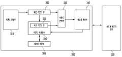
컨트롤러(200)는 커맨드 생성부(210), 메인 커맨드 큐(220), 메모리 제어부(230) 및 커맨드 제거부(240)를 포함할 수 있다.The
커맨드 생성부(210)는 컨트롤러(200)의 제반 동작을 제어하도록 구성된다. 커맨드 생성부(210)는 커맨드를 생성하고 생성된 커맨드를 메인 커맨드 큐(220)에 입력하도록 구성된다.The
실시 예로서, 커맨드 생성부(210)는 호스트로부터의 요청이 수신될 때 요청에 대응하는 커맨드를 생성하고 생성된 커맨드를 메인 커맨드 큐(220)에 입력할 것이다. 호스트로부터의 요청에 대응하는 커맨드는 프로그램, 읽기 또는 소거 커맨드 중 어느 하나일 수 있다.As an embodiment, the
실시 예로서, 커맨드 생성부(210)는 호스트로부터의 요청 없이 커맨드를 생성하고, 그것을 메인 커맨드 큐(220)에 입력할 수 있다. 예를 들면, 커맨드 생성부(210)는 반도체 메모리 장치(100)의 웨어 레벨링(wear leveling)을 위한 동작들, 반도체 메모리 장치(100)의 가비지 컬렉션(garbage collection)을 위한 동작들과 같은 배경(background) 동작들을 위해 커맨드를 생성할 수 있다.As an embodiment, the
실시 예로서, 커맨드 생성부(210)는 플래시 변환 레이어(Flash Translation Layer)의 기능을 수행한다. 커맨드 생성부(210)는 요청에 포함된 논리 블록 어드레스(Logical Block Address)를 물리 블록 어드레스로 변환한다. 커맨드 생성부(210)는 물리 블록 어드레스를 컨트롤러(200) 내부의 저장부(미도시)에 해당 커맨드와 관련하여 저장할 것이다. 플래시 변환 레이어는 호스트로부터 수신되는 논리 어드레스를 플래시 메모리 장치(100)의 물리 어드레스로 변환하는 수단을 제공한다. 플래시 변환 레이어는 논리 어드레스 및 물리 어드레스 사이의 사상(mapping) 관계에 대한 정보를 테이블화하여 유지할 수 있다.In an embodiment, the
메인 커맨드 큐(220)는 커맨드 생성부(210) 및 메모리 제어부(230) 사이에 연결된다. 메인 커맨드 큐(220)는 선입 선출(First In First Out) 방식에 따라 관리된다. 메인 커맨드 큐(220)는 커맨드 생성부(210)로부터 커맨드를 수신하고, 메모리 제어부(230)로 커맨드를 출력한다. 메인 커맨드 큐(220)에 저장된 커맨드들은 반도체 메모리 장치(100)와 컨트롤러(200)의 내부 상태에 따라 순차적으로 또는 랜덤하게 수행될 수 있다.The
메모리 제어부(230)는 커맨드 생성부(210)에서 생성된 커맨드에 따라 반도체 메모리 장치(100)와 통신할 수 있다. 메모리 제어부(230)는 커맨드 생성부(210)의 제어에 응답하여 동작할 수 있다. 메모리 제어부(230)는 메인 커맨드 큐(220)로부터 출력되는 커맨드를 반도체 메모리 장치(100)에 전송함으로써 반도체 메모리 장치를 제어한다. 메모리 제어부(230)는 커맨드와 함께 해당 커맨드에 대응하는 어드레스를 반도체 메모리 장치(100)에 전송할 수 있다.The
선택된 페이지에 대한 읽기 커맨드를 전송하는 것은, 읽기 커맨드, 그리고 선택된 페이지를 가리키는 물리 블록 어드레스를 전송함을 의미한다. 선택된 페이지에 대한 프로그램 커맨드를 전송하는 것은, 프로그램 커맨드, 선택된 페이지를 가리키는 물리 블록 어드레스, 그리고 프로그램 될 데이터를 전송함을 의미한다. 선택된 메모리 블록에 대한 소거 커맨드를 전송하는 것은, 소거 커맨드, 그리고 선택된 메모리 블록을 가리키는 물리 블록 어드레스를 전송함을 의미한다.Transmitting a read command to the selected page implies sending a read command and a physical block address pointing to the selected page. Transmitting the program command for the selected page means transmitting the program command, the physical block address pointing to the selected page, and the data to be programmed. Transmitting the erase command for the selected memory block means transmitting the erase command and the physical block address indicating the selected memory block.
반도체 메모리 장치(100)의 메모리 셀 어레이(110)를 구성하는 메모리 블록들(BLK0~BLKz)에는 결함이 생길 수 있다. 결함이 있는 블록은 배드 블록(bad block)으로 명명될 수 있다. 배드 블록은 다양한 원인에 의해 발생할 수 있다. 예시적으로, 열 페일(column fail), 간섭 문제(disturbance), 마모(wear-out) 등에 의해 배드 블록이 발생될 수 있다.The memory blocks BLK0 to BLKz constituting the
배드 블록 발생시에, 반도체 메모리 장치(100)는 컨트롤러(200)가 전달한 커맨드, 예를 들어 소거 커맨드 또는 프로그램 커맨드의 수행을 실패할 수 있다. 반도체 메모리 장치(100)는 커맨드의 수행 실패 신호를 컨트롤러(200)로 전송한다.When the bad block is generated, the
메모리 제어부(230)는 컨트롤러(200)가 전달한 커맨드에 대해서 반도체 메모리 장치(100)의 커맨드 수행 결과를 수신한다.The
소거 커맨드 또는 프로그램 커맨드의 수행이 실패한 경우, 메인 메모리 큐(220)에 저장된 후속하는 커맨드들 중에는 실패한 커맨드의 물리 블록 어드레스와 동일한 물리 블록 어드레스에 대한 커맨드가 포함될 수 있다. 따라서, 메인 커맨드 큐(220)에 포함된 커맨드들 중에서 수행할 필요가 없는 커맨드들을 제거할 필요가 있다.Among the subsequent commands stored in the
커맨드 제거부(240)는 메인 커맨드 큐(220)와 메모리 제어부(230) 사이에 연결될 수 있다. 커맨드 제거부(240)는 메인 커맨드 큐(220)에 포함된 커맨드들 중에서 수행할 필요가 없는 커맨드들을 제거한다. 커맨드 제거부(240)는 수행할 필요가 없는 커맨드들을 구별하기 위해, 반도체 메모리 장치(100)로부터 커맨드의 수행 결과를 수신할 수 있다. 예를 들어, 메모리 제어부(230)는 반도체 메모리 장치(100)로부터 수신한 커맨드 수행 결과를 커맨드 제거부(240)에 전달 할 수 있다.The
예를 들면, 커맨드 제거부(240)는 메모리 제어부(230)로부터 실패한 커맨드 및 해당 커맨드에 대응하는 물리 블록 어드레스를 전달 받을 수 있다.For example, the
커맨드 제거부(240)는 메인 메모리 큐(220)에서 실패한 커맨드의 연관 커맨드들을 검색할 수 있다. 연관 커맨드들은 실패한 커맨드에 대응하는 물리 블록 어드레스와 동일한 물리 블록 어드레스에 대한 커맨드들일 수 있다.The
실시 예에서 연관 커맨드들은 실패한 커맨드에 대응하는 물리 블록 어드레스와 상이한 물리 블록 어드레스를 가질 수 있다. 구체적으로, 반도체 메모리 장치(100)는 복수의 커맨드들을 수행하여 달성되는 하나의 동작을 수행할 수 있다. 예를 들어 반도체 메모리 장치(100)는 가비지 컬렉션, 웨어 레벨링, 카피 백, 머지 및 베드블록 메니지먼트 등 복수의 커맨드들을 수행하여 달성되는 하나의 동작을 수행할 수 있다. 하나의 동작을 실행하기 위해 필요한 동작 커맨드들은 복수의 커맨드들을 포함할 수 있다. 실시 예에서 연관 커맨드들은 실패한 커맨드가 속하는 동작 커맨드들일 수 있다. 실시 예에서 복수의 커맨드들은 프로그램, 읽기 또는 소거 커맨드들을 포함할 수 있다.In an embodiment, the associate commands may have a physical block address different from the physical block address corresponding to the failed command. In particular, the
커맨드 제거부(240)는 검색된 연관 커맨드들을 메인 메모리 큐(220)에서 제거할 수 있다. 커맨드 제거부(240)는 메인 커맨드 큐(220)의 커맨드들을 엑세스 할 수 있다. 커맨드 제거부(240)가 메인 메모리 큐(220)에서 연관 커맨드들을 제거하면, 메인 메모리 큐(220)는 후속하는 커맨드를 디큐하여 메모리 제어부(230)로 전달한다.The
도면에는 도시되어 있지 않지만, 컨트롤러는 반도체 메모리 장치(100)와 통신하기 위한 메모리 인터페이스를 더 포함할 수 있다. 메모리 인터페이스는 반도체 메모리 장치(100)와 통신하기 위한 프로토콜을 포함한다. 예를 들면, 메모리 인터페이스는 낸드(NAND) 인터페이스, 노어(NOR) 인터페이스 등과 같은 플래시 인터페이스들 중 적어도 하나를 포함할 수 있다.Although not shown in the drawings, the controller may further include a memory interface for communicating with the
또한, 컨트롤러(200)는 호스트 및 컨트롤러(200) 사이의 데이터 교환을 수행하기 위해 호스트 인터페이스를 더 포함할 수 있다. 호스트 인터페이스는 호스트와 컨트롤러(200)간에 통신하기 위한 프로토콜을 포함한다. 예시적으로, 컨트롤러(200)는 USB(Universal Serial Bus) 프로토콜, MMC(multimedia card) 프로토콜, PCI(peripheral component interconnection) 프로토콜, PCI-E(PCI-express) 프로토콜, ATA(Advanced Technology Attachment) 프로토콜, Serial-ATA 프로토콜, Parallel-ATA 프로토콜, SCSI(smallcomputer small interface) 프로토콜, ESDI(enhanced small disk interface) 프로토콜, 그리고 IDE(Integrated Drive Electronics) 프로토콜 등과 같은 다양한 인터페이스 프로토콜들 중 적어도 하나를 통해 외부(호스트)와 통신하도록 구성된다.In addition, the
또한 컨트롤러(200)는 저장부를 더 포함할 수 있다. 저장부는 프로세서(220)의 동작 메모리로 이용될 수 있으며, 반도체 메모리 장치(100) 및 호스트(Host) 사이의 버퍼 메모리로 이용될 수 있으며, 반도체 메모리 장치(100) 및 호스트(Host) 사이의 캐시 메모리로 이용될 수 있다. 또한, 반도체 메모리 장치(100)로부터 입력된 데이터를 임시 자정하는 버퍼로 사용될 수도 있다. 예시적으로, 저장부는 SRAM(Static RAM), DRAM(Dynamic RAM), SDRAM(Synchronous DRAM), PRAM(Phase-change RAM), MRAM(Magnetic RAM), RRAM(Resistive RAM), FRAM(Ferroelectric RAM), 노어 플래시 메모리 등과 같이, 랜덤 액세스가 가능한 다양한 메모리들 중 적어도 하나를 포함할 수 있다.The
도 3은 도 1의 반도체 메모리 장치의 구조를 나타낸 블록도이다.3 is a block diagram showing the structure of the semiconductor memory device of FIG.
도 3을 참조하면, 반도체 메모리 장치(100)는 메모리 셀 어레이(110) 및 주변 회로(120, peripheral circuit)를 포함한다.Referring to FIG. 3, the
메모리 셀 어레이(110)는 복수의 메모리 블록들(BLK0~BLKz)을 포함한다. 복수의 메모리 블록들(BLK0~BLKz)은 행 라인들(RL)을 통해 어드레스 디코더(121)에 연결되고, 비트 라인들(BL1~BLm)을 통해 읽기 및 쓰기 회로(123)에 연결된다. 복수의 메모리 블록들(BLK0~BLKz) 각각은 복수의 메모리 셀들을 포함한다. 실시 예로서, 복수의 메모리 셀들은 불휘발성(nonvolatile) 메모리 셀들이다.The
제 0 내지 제 z 메모리 블록들(BLK0~BLKz) 각각은 복수의 셀 스트링들을 포함한다. 예를 들면, 제 1 내지 제 m 셀 스트링들은 각각 제 1 내지 제 m 비트 라인들(BL1~BLm)에 연결될 수 있다. 제 1 내지 제 m 셀 스트링들 각각은 드레인 선택 트랜지스터, 직렬 연결된 복수의 메모리 셀들 및 소스 선택 트랜지스터를 포함할 수 있다. 드레인 선택 트랜지스터(DST)는 드레인 선택 라인(DSL)에 연결될 수 있다. 제 1 내지 제 n 메모리 셀들은 각각 제 1 내지 제 n 워드 라인들에 연결될 수 있다. 하나의 워드 라인에 연결된 제1 내지 제 n 메모리 셀들은 하나의 페이지(PG)를 구성할 수 있다. 소스 선택 트랜지스터(SST)는 소스 선택 라인(SSL)에 연결될 수 있다. 드레인 선택 트랜지스터(DST)의 드레인 측은 해당 비트 라인에 연결될 수 있다. 제 1 내지 제 m 셀 스트링들의 드레인 선택 트랜지스터들은 각각 제 1 내지 제 m 비트 라인들(BL1~BLm)에 연결된다. 소스 선택 트랜지스터(SST)의 소스 측은 공통 소스 라인(CSL)에 연결될 수 있다. 실시 예로서, 공통 소스 라인(CSL)은 제 1 내지 제 z 메모리 블록들(BLK1~BLKz)에 공통 연결될 수 있다. 드레인 선택 라인(DSL1), 제 1 내지 제 n 워드 라인들(WL1~WLn), 및 소스 선택 라인(SSL1)은 행 라인들(RL)에 포함된다. 드레인 선택 라인(DSL), 제 1 내지 제 n 워드 라인들(WL1~WLn), 및 소스 선택 라인(SSL)은 어드레스 디코더(121)에 의해 제어된다. 공통 소스 라인(CSL)은 제어 로직(125)에 의해 제어된다. 제 1 내지 제 m 비트 라인들(BL1~BLm)은 읽기 및 쓰기 회로(123)에 의해 제어된다..Each of the zeroth through z memory blocks BLK0 through BLKz includes a plurality of cell strings. For example, the first to m-th cell strings may be connected to the first to m-th bit lines BL1 to BLm, respectively. Each of the first through m-th cell strings may include a drain select transistor, a plurality of memory cells connected in series, and a source select transistor. The drain select transistor DST may be connected to the drain select line DSL. The first to n < th > memory cells may be connected to the first to n < th > word lines, respectively. The first to n-th memory cells connected to one word line may constitute one page (PG). The source select transistor SST may be connected to the source select line SSL. And the drain side of the drain select transistor DST may be connected to the corresponding bit line. The drain selection transistors of the first to m-th cell strings are connected to the first to m-th bit lines BL1 to BLm, respectively. The source side of the source select transistor SST may be connected to the common source line CSL. As an embodiment, the common source line CSL may be connected in common to the first to z-th memory blocks BLK1 to BLKz. The drain select line DSL1, the first to nth word lines WL1 to WLn, and the source select line SSL1 are included in the row lines RL. The drain select line DSL, the first to nth word lines WL1 to WLn, and the source select line SSL are controlled by the
주변 회로(120)는 어드레스 디코더(121), 전압 발생기(122), 읽기 및 쓰기 회로(123), 데이터 입출력 회로(124) 및 제어 로직(125)을 포함한다.The
어드레스 디코더(121)는 행 라인들(RL)을 통해 메모리 셀 어레이(110)에 연결된다. 어드레스 디코더(121)는 제어 로직(125)의 제어에 응답하여 동작하도록 구성된다. 어드레스 디코더(121)는 제어 로직(125)을 통해 어드레스(ADDR)를 수신한다.The
실시 예로서, 반도체 메모리 장치(100)의 프로그램 동작 및 읽기 동작은 페이지 단위로 수행된다.As an embodiment, the program operation and the read operation of the
프로그램 및 읽기 동작 시에, 제어 로직(125)이 수신한 어드레스(ADDR)는 블록 어드레스 및 행 어드레스를 포함할 것이다. 어드레스 디코더(121)는 수신된 어드레스(ADDR) 중 블록 어드레스를 디코딩하도록 구성된다. 어드레스 디코더(121)는 디코딩된 블록 어드레스에 따라 메모리 블록들(BLK1~BLKz) 중 하나의 메모리 블록을 선택한다.During a program and read operation, the address ADDR received by the
어드레스 디코더(121)는 수신된 어드레스(ADDR) 중 행 어드레스를 디코딩하도록 구성된다. 어드레스 디코더(121)는 디코딩된 행 어드레스에 따라 전압 발생기(122)로부터 제공받은 전압들을 행 라인들(RL)에 인가하여 선택된 메모리 블록의 하나의 워드 라인을 선택한다.The
소거 동작 시에 어드레스(ADDR)는 블록 어드레스를 포함한다. 어드레스 디코더(121)은 블록 어드레스를 디코딩하고, 디코딩된 블록 어드레스에 따라 하나의 메모리 블록을 선택한다. 소거 동작은 하나의 메모리 블록 전체 또는 일부에 대해서 수행될 수 있다.In the erase operation, the address ADDR includes a block address. The
어드레스 디코더(121)는 수신된 어드레스(ADDR) 중 행 어드레스들을 디코딩하도록 구성된다. 어드레스 디코더(121)는 디코딩된 행 어드레스들에 따라 전압 발생기(122)로부터 제공받은 전압들을 행 라인들(RL)들에 인가하여 선택된 메모리 블록의 적어도 하나의 워드 라인을 선택한다.The
실시 예로서, 어드레스 디코더(121)은 블록 디코더, 워드라인 디코더 및 어드레스 버퍼 등을 포함할 수 있다.As an example, the
전압 발생기(122)는 반도체 메모리 장치(100)에 공급되는 외부 전원 전압을 이용하여 복수의 전압들을 발생하도록 구성된다. 전압 발생기(122)는 제어 로직(125)의 제어에 응답하여 동작한다.The
실시 예로서, 전압 발생기(122)는 외부 전원 전압을 레귤레이팅하여 내부 전원 전압을 생성할 수 있다. 전압 발생기(122)에서 생성된 내부 전원 전압은 반도체 메모리 장치(100)의 동작 전압으로서 사용된다.In an embodiment, the
실시 예로서, 전압 발생기(122)는 외부 전원 전압 또는 내부 전원 전압을 이용하여 복수의 전압들을 생성할 수 있다. 예를 들면, 전압 발생기(122)는 내부 전원 전압을 수신하는 복수의 펌핑 커패시터들을 포함하고, 제어 로직(125)의 제어에 응답하여 복수의 펌핑 커패시터들을 선택적으로 활성화하여 복수의 전압들을 생성할 것이다. 생성된 복수의 전압들은 어드레스 디코더(121)에 의해 선택된 워드 라인들에 인가된다.In an embodiment, the
프로그램 동작 시에, 전압 발생기(122)는 고전압의 프로그램 펄스 및 프로그램 펄스보다 낮은 패스 펄스를 생성할 것이다. 읽기 동작 시에, 전압 발생기(130)는 리드 전압 및 리드 전압보다 높은 패스 전압을 생성할 것이다. 소거 동작 시에, 전압 발생기(130)는 소거 전압을 생성할 것이다.During program operation, the
읽기 및 쓰기 회로(123)는 제 1 내지 제 m 페이지 버퍼들(PB1~PBm)을 포함한다. 제 1 내지 제 m 페이지 버퍼들(PB1~PBm)은 각각 제 1 내지 제 m 비트 라인들(BL1~BLm)을 통해 메모리 셀 어레이(110)에 연결된다. 제 1 내지 제 m 페이지 버퍼들(PB1~PBm)은 제어 로직(125)의 제어에 응답하여 동작한다.The read and write
제 1 내지 제 m 페이지 버퍼들(PB1~PBm)은 데이터 입출력 회로(124)와 데이터를 통신한다. 프로그램 시에, 제 1 내지 제 m 페이지 버퍼들(PB1~PBm)은 데이터 입출력 회로(124) 및 데이터 라인들(DL)을 통해 저장될 데이터(DATA)를 수신한다.The first to m < th > page buffers PB1 to PBm communicate data with the data input /
프로그램 동작 시, 제 1 내지 제 m 페이지 버퍼들(PB1~PBm)은 선택된 워드 라인에 프로그램 펄스가 인가될 때, 저장될 데이터(DATA)를 데이터 입출력 회로(124)를 통해 수신한 데이터(DATA)를 비트 라인들(BL1~BLm)을 통해 선택된 메모리 셀들에 전달할 것이다. 전달된 데이터(DATA)에 따라 선택된 페이지의 메모리 셀들은 프로그램 된다. 프로그램 허용 전압(예를 들면, 접지 전압)이 인가되는 비트 라인과 연결된 메모리 셀은 상승된 문턱 전압을 가질 것이다. 프로그램 금지 전압(예를 들면, 전원 전압)이 인가되는 비트 라인과 연결된 메모리 셀의 문턱 전압은 유지될 것이다. 프로그램 검증 동작 시에, 제 1 내지 제 m 페이지 버퍼들(PB1~PBm)은 선택된 메모리 셀들로부터 비트 라인들(BL1~BLm)을 통해 페이지 데이터를 읽는다.The first to m-th page buffers PB1 to PBm transmit data (DATA) to be stored to the data (DATA) received through the data input /
읽기 동작 시, 읽기 및 쓰기 회로(123)는 선택된 페이지의 메모리 셀들로부터 비트 라인들(BL)을 통해 데이터(DATA)를 읽고, 읽어진 데이터(DATA)를 입출력 회로(124)로 출력한다. 소거 동작 시에, 읽기 및 쓰기 회로(123)는 비트 라인들(BL)을 플로팅(floating) 시킬 수 있다.In a read operation, the read and write
실시 예로서, 읽기 및 쓰기 회로(123)는 열 선택 회로를 포함할 수 있다.As an example, the read and write
데이터 입출력 회로(124)는 데이터 라인들(DL)을 통해 제 1 내지 제 m 페이지 버퍼들(PB1~PBm)에 연결된다. 데이터 입출력 회로(124)는 제어 로직(125)의 제어에 응답하여 동작한다. 프로그램 시에, 데이터 입출력 회로(124)는 외부 컨트롤러(미도시)로부터 저장될 데이터(DATA)를 수신한다.The data input /
제어 로직(125)은 어드레스 디코더(121), 전압 발생기(122), 읽기 및 쓰기 회로(123) 및 데이터 입출력 회로(124)에 연결된다. 제어 로직(125)은 반도체 메모리 장치(100)의 전반적인 동작을 제어할 수 있다. 제어 로직(125)은 외부 컨트롤러로부터 커맨드(CMD) 및 어드레스(ADDR)를 수신한다. 제어 로직(125)은 커맨드(CMD)에 응답하여 어드레스 디코더(121), 전압 발생기(122), 읽기 및 쓰기 회로(123) 및 데이터 입출력 회로(124)를 제어하도록 구성된다.The
도 4는 본 발명의 실시 예에 따라 커맨드들을 메인 커맨드 큐로부터 제거하는 방법을 설명하기 위한 도면이다.4 is a diagram for explaining a method of removing commands from a main command queue according to an embodiment of the present invention.
도 4를 참조하면 반도체 메모리 장치(100)에 포함된 복수의 메모리 블록들 중에는 유효한(valid) 데이터와 인식 불가능한(invalid) 데이터가 저장되어 있는 메모리 블록(BLK0)(40)과 데이터가 저장되어 있지 않는 비어있는(empty) 블록(BLK1)(41)이 포함될 수 있다. 예를 들어, 제 0 메모리 블록(BLK0)(40)은 제0 페이지(PG0) 내지 제2 페이지(PG2)에 유효한(valid) 데이터와 인식 불가능한(invalid) 데이터가 함께 저장되어 있다. 제1 메모리 블록(BLK1)(41)에는 데이터가 저장되어 있지 않을 수 있다. 반도체 메모리 장치는 메모리 블록의 유효공간을 더 넓히기 위하여 인식 불가능한(invalid) 페이지들을 관리 할 수 있다. 예를 들어 반도체 메모리 장치(100)는 가비지 컬렉션(garbage collection)과 같은 동작을 통해 유효한(valid) 데이터들을 비어있는 블록에 저장하고, 베드 블록 전체를 소거 시킴으로써 메모리 용량을 확보할 수 있다.4, among the plurality of memory blocks included in the
도 4의 메인 커맨드 큐(220)는 제0 메모리 블록(41)의 유효한(valid) 데이터들을 제1 메모리 블록(42)으로 옮기기 위한 커맨드들을 포함한다.The
메인 커맨드 큐(220)는 헤드 어드레스(HA)와 테일 어드레스(TA) 사이에서 복수의 커맨드들(CMD0~CMDp)을 저장한다. 제 0 내지 제 p 커맨드들(CMD0~CMDp)은 다양한 타입들의 커맨드들일 수 있다. 제 0 내지 제 p 커맨드들(CMD0~CMDp) 각각은, 예를 들면 프로그램 커맨드, 읽기 커맨드, 및 소거 커맨드 중 어느 하나일 수 있다.The
헤드 어드레스(HA)는 메인 커맨드 큐(220)의 첫 번째 커맨드(CMD0)를 가리킨다. 테일 어드레스(TA)는 메인 커맨드 큐(220)의 마지막 커맨드(CMDp)를 가리킨다. 메인 커맨드 큐(220)는 선입 선출 방식에 따라 관리된다. 따라서, 커맨드 생성부(210)에 의해 복수의 커맨드들(RCMD1, CMD1~CMDp)이 생성되고, 복수의 커맨드들(RCMD1, CMD1~CMDp)은 그것들이 입력된 순서대로 메인 커맨드 큐(220)에 저장될 것이다. 메인 커맨드 큐(220)에 새로운 커맨드가 입력되면, 테일 어드레스(TA)는 해당 새로운 커맨드를 가리킬 것이다. 메인 커맨드 큐(220)의 헤드 어드레스(HA)가 가리키는 커맨드가 출력될 것이다.The head address HA indicates the first command CMD0 of the
반도체 메모리 장치는 가비지 컬렉션, 웨어 레벨링, 카피 백, 머지 및 베드블록 메니지먼트 등 복수의 커맨드들을 수행하여 달성되는 하나의 동작을 수행할 수 있다. 이 경우 하나의 동작을 수행하기 위해 필요한 동작 커맨드들은 복수의 커맨드들을 포함할 수 있다. 실시 예에서 복수의 커맨드들은 프로그램, 읽기 또는 소거 커맨드들을 포함할 수 있다.The semiconductor memory device may perform one operation that is accomplished by performing a plurality of commands, such as garbage collection, wear leveling, copyback, merge, and bed block management. In this case, the operation commands necessary for performing one operation may include a plurality of commands. In an embodiment, the plurality of commands may include program, read or erase commands.
도 4에서 제0 내지 제7 커맨드(CMD0~CMD7)들은 제0 메모리 블록(40)의 유효한 데이터들을 제1 메모리 블록(41)으로 저장하는 동작을 수행하기 위한 커맨드들이다.In FIG. 4, the 0th to 7th commands CMD0 to CMD7 are commands for performing the operation of storing the valid data of the
제0 커맨드(CMD0)는 제1 메모리 블록(41)을 소거하기 위한 소거 커맨드(ERASE)이다. 제1 커맨드(CMD1)는 제0 메모리 블록(40)의 제0 페이지(PG0)에 대한 읽기 커맨드(READ)이다. 제2 커맨드(CMD2)는 제1 메모리 블록(41)의 제0 페이지(PG0)에 대한 프로그램 커맨드(PGM)이다. 제3 커맨드(CMD3)는 제0 메모리 블록(40)의 제1 페이지(PG1)에 대한 읽기 커맨드(READ)이다. 제4 커맨드(CMD4)는 제1 메모리 블록(41)의 제1 페이지(PG1)에 대한 프로그램 커맨드(PGM)이다. 제5 커맨드(CMD5)는 제0 메모리 블록(40)의 제2 페이지(PG2)에 대한 읽기 커맨드(READ)이다. 제6 커맨드(CMD6)는 제1 메모리 블록(41)의 제2 페이지(PG2)에 대한 프로그램 커맨드(PGM)이다. 제7 커맨드(CMD7)는 제0 메모리 블록(40)에 대한 소거 커맨드(ERASE)이다. 제 0 커맨드(CMD0) 내지 제7 커맨드(CMD7)를 통해 제 0메모리 블록(40)의 유효한(valid) 데이터가 제1 메모리 블록(41)으로 기록될 수 있다.The 0th command (CMD0) is an erase command (ERASE) for erasing the first memory block (41). The first command CMD1 is a read command READ for the 0th page PG0 of the
제 8 내지 제n 커맨드(CMD8~CMDn)는 제0 메모리 블록 및 제1 메모리 블록과 상이한 메모리 블록들에 대한 커맨드일 수 있다. 또한 제 n+1 커맨드 내지 제p 커맨드(CMDn+1~CMDp)는 제 8 내지 제n 커맨드(CMD8~CMDn)와 상이한 메모리 블록에 대한 커맨드일 수 있다. 예를 들어, 제 8 내지 제n 커맨드(CMD8~CMDn)와 제 n+1 커맨드 내지 제p 커맨드(CMDn+1~CMDp)는 반도체 메모리 장치의 임의의 동작을 수행하기 위한 커맨드들일 수 있다. 이 경우 제0 내지 제7 커맨드(CMD0~CMD7)들, 제 8 내지 제n 커맨드(CMD8~CMDn) 및 제 n+1 커맨드 내지 제p 커맨드(CMDn+1~CMDp)는 각각 독립적인 동작을 수행하는 동작 커맨드들일 수 있다.The eighth to nth commands CMD8 to CMDn may be commands for memory blocks different from the 0th memory block and the first memory block. The n + 1-th command to the p-th command CMDn + 1 to CMDp may be commands for memory blocks different from the eighth to n-th commands CMD8 to CMDn. For example, the eighth to nth commands CMD8 to CMDn and the (n + 1) th to (p) commands CMDn + 1 to CMDp may be commands for performing an arbitrary operation of the semiconductor memory device. In this case, the 0th to 7th commands CMD0 to CMD7, the 8th to nth commands CMD8 to CMDn, and the (n + 1) th command to the p command CMDn + 1 to CMDp perform independent operations Lt; / RTI >
메인 메모리 큐(220)의 커맨드들이 순차적으로 실행되는 도중에 어느 한 커맨드의 실행이 실패할 수 있다. 이 경우, 후속하는 커맨드들 중에 실패한 커맨드와 연관된 커맨드들은 실행될 필요가 없으므로, 메인 메모리 큐(220)로부터 제거되어야 한다.Execution of any one of the commands may fail while the commands of the
반도체 메모리 장치의 제0 커맨드의 수행이 실패하면, 제1 내지 제7 커맨드(CMD1~CMD7)들은 수행될 필요가 없으므로, 메인 메모리 큐(220)로부터 제거될 필요가 있다. 이를 위해 컨트롤러는 실패한 커맨드와 연관된 커맨드들을 제거할 수 있다. 도 4에서 제0 커맨드의 수행이 실패하면, 컨트롤러는 제1 내지 제7 커맨드(CMD1~CMD7)들을 메인 메모리 큐(220)로부터 제거하고, 제8 커맨드(CMD8)를 디큐하여 반도체 메모리 장치로 전송한다.If the execution of the 0th command of the semiconductor memory device fails, the first to seventh commands CMD1 to CMD7 do not need to be executed, and therefore need to be removed from the
도 5는 도 1의 컨트롤러의 동작을 나타낸 순서도이다.5 is a flowchart showing the operation of the controller of FIG.
도 5를 참조하면, 501 단계에서, 컨트롤러는 소거 또는 프로그램 커맨드의 수행이 실패하였는지를 판단할 수 있다. 컨트롤러는 반도체 메모리 장치로부터 소거 또는 프로그램 커맨드의 수행 결과를 반도체 메모리 장치로부터 수신한다. 반도체 메모리 장치가 소거 또는 프로그램 커맨드의 수행이 실패하지 않으면 계속해서 501단계로 회귀한다.Referring to FIG. 5, in
501 단계에서 판단한 결과, 반도체 메모리 장치가 소거 또는 프로그램 커맨드의 수행에 실패하면, 503 단계에서, 컨트롤러는 메인 메모리 큐에서 실패한 커맨드의 연관 커맨드들을 검색할 수 있다. 연관 커맨드들은 실패한 커맨드에 대응하는 물리 블록 어드레스와 동일한 물리 블록 어드레스에 대한 커맨드들일 수 있다.As a result of the determination in
실시 예에서, 연관 커맨드들은 실패한 커맨드가 속하는 동작 커맨드들일 수 있다. 즉, 반도체 메모리 장치는 가비지 컬렉션, 웨어 레벨링, 카피 백, 머지 및 베드블록 메니지먼트 등 복수의 커맨드들을 수행하여 달성되는 하나의 동작을 수행할 수 있다. 이 경우 하나의 동작을 수행하기 위해 필요한 동작 커맨드들은 복수의 커맨드들을 포함할 수 있다. 실시 예에서 복수의 커맨드들은 프로그램, 읽기 또는 소거 커맨드들을 포함할 수 있다.In an embodiment, the association commands may be operation commands to which the failed command belongs. That is, the semiconductor memory device can perform one operation that is accomplished by executing a plurality of commands such as garbage collection, wear leveling, copyback, merge, and bed block management. In this case, the operation commands necessary for performing one operation may include a plurality of commands. In an embodiment, the plurality of commands may include program, read or erase commands.
505 단계에서 컨트롤러는 검색된 연관 커맨드들을 메인 메모리 큐에서 제거할 수 있다. 컨트롤러는 연관 커맨드들을 제거하고, 후속하는 커맨드를 디큐하여 반도체 메모리 장치로 전송할 수 있다.In
도 6은 본 발명의 다른 실시 예에 따른 컨트롤러의 구조를 나타낸 블록도이다.6 is a block diagram illustrating a structure of a controller according to another embodiment of the present invention.
도 6을 참조하면, 반도체 메모리 장치(100)는 도 1을 참조하여 설명된 반도체 메모리 장치(100)와 동일하다.Referring to FIG. 6, the
컨트롤러(300)는 반도체 메모리 장치(100)를 제어하도록 구성된다. 컨트롤러(300)는 호스트(미도시)로부터의 요청에 응답하여 반도체 메모리 장치(100)를 액세스하도록 구성된다. 예를 들면, 컨트롤러(300)는 반도체 메모리 장치(100)의 읽기 동작, 프로그램 동작, 소거 동작, 그리고 배경(background) 동작을 제어하도록 구성된다. 컨트롤러(300)는 반도체 메모리 장치(100) 및 호스트 사이에서 인터페이스를 제공하도록 구성된다. 컨트롤러(300)는 반도체 메모리 장치(100)를 제어하기 위한 펌웨어(firmware)를 구동하도록 구성된다.The
컨트롤러(300)는 커맨드 생성부(310), 메인 커맨드 큐(320), 커맨드 선택부(330), 메모리 제어부(340), 커맨드 미러링부(350), 및 미러링 저장부(360)를 포함한다.The
커맨드 생성부(310) 및 메인 커맨드 큐(320)는 도 1을 참조하여 설명된 커맨드 생성부(210) 및 메인 커맨드 큐(220)와 같은 구성이고 같은 방식으로 동작할 수 있다.The
커맨드 선택부(330)는 메인 커맨드 큐(320), 커맨드 미러링부(350) 및 메모리 제어부(340)에 연결된다. 커맨드 선택부(330)는 커맨드 미러링부(360)의 제어에 따라 메인 커맨드 큐(320) 및 서브 커맨드 큐(355) 중 어느 하나를 선택하도록 구성된다. 예를 들면, 커맨드 미러링부(350)로부터 제공되는 제어 신호가 디스에이블될 때 커맨드 선택부(330)는 메인 커맨드 큐(320)에 저장된 커맨드를 출력하고, 출력된 커맨드를 메모리 제어부(340)에 전달한다. 그리고, 커맨드 미러링부(350)로부터 제공되는 제어 신호가 인에이블될 때, 커맨드 선택부(330)는 서브 커맨드 큐(355)에 저장된 커맨드를 출력하고, 출력된 커맨드를 메모리 제어부(340)에 전달한다.The
메모리 제어부(340)는 입력되는 커맨드에 따라 반도체 메모리 장치(100)와 통신할 수 있다. 메모리 제어부(340)는 커맨드 생성부(310)의 제어에 응답하여 동작할 수 있다. 메모리 제어부(340)는 커맨드 선택부(330)를 통해 수신된 커맨드를 반도체 메모리 장치(100)에 전송함으로써 반도체 메모리 장치를 제어한다. 메모리 제어부(340)는 커맨드와 함께 해당 커맨드에 대응하는 어드레스를 반도체 메모리 장치(100)에 전송할 수 있다. 실시 예에서, 메모리 제어부(340)는 컨트롤러(200)가 전달한 커맨드에 대해서 반도체 메모리 장치(100)의 커맨드 수행 결과를 수신한다.The
커맨드 미러링부(350)는 메인 커맨드 큐(320), 커맨드 선택부(330), 메모리 제어부(340) 및 미러링 저장부(360)에 연결된다. 본 발명의 실시 예에 따르면, 커맨드 미러링부(350)는 메인 커맨드 큐(320)에 입력된 커맨드를 미러링하여 미러링 커맨드를 생성하고, 생성된 미러링 커맨드를 미러링 저장부(360)에 저장할 수 있다. 실시 예에서, 미러링 커맨드는 반도체 메모리 장치의 동작을 나타내는 커맨드와 커맨드에 대응하는 물리 블록 어드레스를 포함할 수 있다.The
실시 예로서, 커맨드 미러링부(350)는 반도체 메모리 장치(100)로부터 커맨드의 수행 결과를 수신할 수 있다. 예를 들어, 커맨드 미러링부(350)는 메모리 제어부(340)로부터 반도체 메모리 장치(100)로부터 수신한 커맨드 수행 결과를 전달 받을 수 있다.As an embodiment, the
커맨드 미러링부(350)는 소거 또는 프로그램 커맨드의 수행이 실패하면, 미러링 저장부(360)에 저장된 미러링 커맨드들을 참조한다.The
커맨드 미러링부(350)는 수신한 커맨드 수행 결과를 기초로 미러링 저장부(360)에 저장된 미러링 커맨드들로부터 연관 커맨드들을 제거할 수 있다. 연관 커맨드들은 실패한 커맨드에 대응하는 물리 블록 어드레스와 동일한 물리 블록 어드레스에 대한 커맨드들일 수 있다.The
다양한 실시 예에서 연관 커맨드들은 실패한 커맨드에 대응하는 물리 블록 어드레스와 상이한 물리 블록 어드레스를 가질 수 있다. 구체적으로, 반도체 메모리 장치(100)는 복수의 커맨드들을 수행하여 달성되는 하나의 동작을 수행할 수 있다. 예를 들어 반도체 메모리 장치(100)는 가비지 컬렉션, 웨어 레벨링, 카피 백, 머지 및 베드블록 메니지먼트 등 복수의 커맨드들을 수행하여 달성되는 하나의 동작을 수행할 수 있다. 하나의 동작을 실행하기 위해 필요한 동작 커맨드들은 복수의 커맨드들을 포함할 수 있다. 실시 예에서 연관 커맨드들은 실패한 커맨드가 속하는 동작 커맨드들일 수 있다. 실시 예에서 복수의 커맨드들은 프로그램, 읽기 또는 소거 커맨드들을 포함할 수 있다.In various embodiments, the associate commands may have a different physical block address than the physical block address corresponding to the failed command. In particular, the
커맨드 미러링부(350)는 실패한 커맨드의 연관 커맨드가 제거된 미러링 커맨드들을 기초로 서브 커맨드 큐(355)를 생성할 수 있다.The
실시 예로서, 커맨드 미러링부(350)는 미러링 커맨드들과 동일한 커맨드들로 구성된 서브 커맨드 큐(355)를 생성할 수 있다. 서브 커맨드 큐(355)는 메인 커맨드 큐(320)와 그 형태가 동일하며, 같은 방법에 의해 동작할 수 있다. 서브 커맨드 큐(355)는 선입 선출(First In First Out) 방식에 따라 관리된다. 서브 커맨드 큐(355)는 커맨드 선택부(330)로 커맨드를 출력한다. 서브 커맨드 큐(355)에 저장된 커맨드들은 반도체 메모리 장치(100)와 컨트롤러(200)의 내부 상태에 따라 순차적으로 또는 랜덤하게 수행될 수 있다.As an example, the
커맨드 미러링부(350)는 커맨드 선택부(330)가 서브 커맨드 큐(355)를 선택하도록 커맨드 선택부(330)를 제어한다. 예를 들면, 커맨드 미러링부(350)는 커맨드 선택부(330)에 전송되는 제어 신호를 인에이블함으로써, 서브 커맨드 큐(355)를 선택하도록 커맨드 선택부(330)를 제어할 수 있다.The
커맨드 선택부(330)는 서브 커맨드 큐(355)에 저장된 커맨드를 디큐하여 메모리 제어부(240)에 제공할 것이다. 메모리 제어부(340)는 제공 받은 커맨드 및 커맨드와 관련하여 저장된 물리 블록 어드레스를 반도체 메모리 장치(100)에 전송할 것이다.The
도 7은 도 6의 컨트롤러의 동작을 나타낸 순서도이다.7 is a flowchart showing the operation of the controller of Fig.
도 7을 참조하면, 701 단계에서, 컨트롤러는 메인 커맨드 큐를 미러링 하여 미러링 커맨드들을 생성한다. 컨트롤러는 생성된 미러링 커맨드들을 별도의 저장부에 저장할 수 있다. 컨트롤러는 호스트의 요청 또는 호스트의 요청과 무관하게 커맨드를 생성할 수 있다. 생성된 커맨드들은 메인 커맨드 큐에 입력된다. 메인 커맨드 큐에 커맨드가 입력되면 컨트롤러는 입력된 커맨드를 미러링하여 미러링 커맨드들을 생성한다. 생성된 미러링 커맨드들은 각각 커맨드와 해당 커맨드에 대응하는 물리 블록 어드레스를 포함할 수 있다. 실시 예에서, 컨트롤러는 커맨드의 물리 블록 어드레스만을 미러링 커맨드로 저장할 수 있다.Referring to FIG. 7, in
703 단계에서, 컨트롤러는 메인 커맨드 큐로부터 커맨드를 반도체 메모리 장치로 출력한다. 구체적으로 컨트롤러는 메인 커맨드 큐에 저장된 커맨드를 디큐하여 반도체 메모리 장치로 전달한다. 컨트롤러는 커맨드와 커맨드에 대응하는 물리 블록 어드레스를 함께 전달할 수 있다.In
705 단계에서, 컨트롤러는 반도체 메모리 장치의 소거 또는 프로그램 커맨드의 수행이 실패하였는지 여부를 판단한다. 703 단계에서 컨트롤러가 반도체 메모리 장치로 커맨드와 물리 블록 어드레스를 전달하면, 컨트롤러는 반도체 메모리 장치로부터 전달된 커맨드의 수행 결과를 수신할 수 있다. 705 단계에서 판단한 결과, 소거 또는 프로그램 커맨드가 실패하지 않으면, 컨트롤러는 703 단계로 회귀하여 메인 커맨드 큐로부터 커맨드를 반도체 메모리 장치로 출력한다. 705 단계에서 판단한 결과, 컨트롤러는 소거 또는 프로그램 커맨드의 실패가 있는 경우 707 단계로 진행한다.In
707 단계에서, 컨트롤러는 저장된 미러링 커맨드들로부터 실패한 커맨드의 연관 커맨드들을 제거한다. 연관 커맨드들은 실패한 커맨드에 대응하는 물리 블록 어드레스와 동일한 물리 블록 어드레스에 대한 커맨드들일 수 있다. 실시 예에서, 연관 커맨드들은 실패한 커맨드가 속하는 동작 커맨드들일 수 있다. 여기서 동작 커맨드들은 하나의 동작을 수행하기 위해 필요한 복수의 커맨드들을 포함할 수 있다. 실시 예에서 복수의 커맨드들은 프로그램, 읽기 또는 소거 커맨드들을 포함할 수 있다.In
709 단계에서, 컨트롤러는 연관 커맨드들이 제거된 미러링 커맨드들을 기초로 서브 커맨드 큐를 생성할 수 있다. 실시 예에서 컨트롤러는 연관 커맨드들이 제거된 미러링 커맨드들과 동일한 커맨드들로 구성된 서브 커맨드 큐를 생성할 수 있다. 실시 예에서, 서브 커맨드 큐는 메인 커맨드 큐와 그 형태가 동일하며, 같은 방법에 의해 동작할 수 있다. 서브 커맨드 큐는 선입 선출(First In First Out) 방식에 따라 관리될 수 있다.In
711 단계에서, 컨트롤러는 서브 커맨드 큐에 저장된 커맨드들 중 하나의 커맨드를 디큐하여 출력한다. 컨트롤러는 서브 커맨드 큐에 저장된 커맨드들을 순차적으로 또는 랜덤하게 출력할 수 있다. 컨트롤러는 서브 커맨드 큐에 저장된 커맨드 및 커맨드와 관련하여 저장된 물리 블록 어드레스를 반도체 메모리 장치에 전송할 것이다.In
도 8은 도 6의 메인 커맨드 큐(320), 미러링 저장부(360) 및 서브 커맨드 큐(355)에 저장된 커맨드들을 보여주는 개념도이다.FIG. 8 is a conceptual diagram showing commands stored in the
도 8를 참조하면, 메인 커맨드 큐(320)는 헤드 어드레스(HA)와 테일 어드레스(TA) 사이에서 복수의 커맨드들(CMD0~CMDp)을 저장한다. 커맨드 생성부(310)는 제 0 내지 제 p 커맨드들(CMD0~CMDp)을 생성할 수 있다. 제 0 내지 제 p 커맨드들(CMD0~CMDp)은 다양한 타입들의 커맨드들일 수 있다. 제 0 내지 제 p 커맨드들(CMD1~CMDp) 각각은, 예를 들면 프로그램 커맨드, 읽기 커맨드, 및 소거 커맨드 중 어느 하나일 수 있다.Referring to FIG. 8, the
헤드 어드레스(HA)는 메인 커맨드 큐(320)의 첫 번째 커맨드(CMD0)를 가리킨다. 테일 어드레스(TA)는 메인 커맨드 큐(320)의 마지막 커맨드(CMDp)를 가리킨다. 메인 커맨드 큐(320)는 선입 선출 방식에 따라 관리될 것이다. 커맨드 생성부(310)에 의해 복수의 커맨드들(CMD0~CMDp)이 생성되고, 복수의 커맨드들(CMD0~CMDp)은 그것들이 입력된 순서대로 메인 커맨드 큐(320)에 저장될 것이다. 메인 커맨드 큐(320)에 새로운 커맨드가 입력되면, 테일 어드레스(TA)는 해당 새로운 커맨드를 가리킬 것이다. 메인 커맨드 큐(320)의 헤드 어드레스(HA)가 가리키는 커맨드가 출력될 것이다.The head address HA indicates the first command CMD0 of the
메인 커맨드 큐(320)에 저장된 커맨드들(CMD0~CMDp)은 미러링 저장부(360)에 미러링된다. 도 8에서, 메인 커맨드 큐(320)의 헤드 어드레스(HA)에 제 0 커맨드(CMD0)가 저장되어 있다. 제 0 커맨드(CMD0)는 미러링되어 미러링 저장부(360)에 미러링 커맨드(MCMD0)로서 저장될 것이다.The commands CMD0 to CMDp stored in the
제 1 내지 제 p 커맨드들(CMD1~CMDp)도 제 0 읽기 커맨드(CMD0)와 마찬가지로 미러링될 수 있음이 이해될 것이다.It will be appreciated that the first to p-th commands CMD1 to CMDp may also be mirrored like the zero read command CMD0.
도 8에서는 제0 내지 제2 커맨드(CMD0~CMD2)들이 하나의 동작 커맨드들을 구성하는 경우를 예로 들어 설명한다. 제3 커맨드(CMD3)는 제0 내지 제2 커맨드(CMD0~CMD2)와 상이한 동작 커맨드를 구성한다. 따라서, 제0 커맨드(CMD0)의 수행이 실패하면, 컨트롤러는 미러링 저장부(360)에 저장된 커맨드 들 중 제0 커맨드(CMD0)의 연관 커맨드들을 제거한다. 제0 커맨드(CMD0)의 연관 커맨드들은 제0 내지 제2 커맨드(CMD0~ CMD2)일 수 있다.In FIG. 8, the case where the 0th to 2nd commands CMD0 to CMD2 constitute one operation command will be described as an example. The third command CMD3 constitutes an operation command different from the 0th to 2nd commands CMD0 to CMD2. Therefore, if the execution of the 0th command CMD0 fails, the controller removes the related commands of the 0th command CMD0 among the commands stored in the
컨트롤러는 미러링 저장부(360)에서 연관 커맨드들을 제거하고, 연관 커맨드들이 제거된 미러링 커맨드들을 기초로 서브 커맨드 큐(355)를 생성할 수 있다. 따라서, 제0 커맨드(CMD0)의 수행이 실패하면, 제0 내지 제2 커맨드(CMD2)가 제거되고, 제3 커맨드(CMD3)가 헤드 어드레스(HA)에 위치하도록 서브 커맨드 큐(355)가 생성될 수 있다.The controller may remove association commands from the
다양한 실시 예에서, 컨트롤러는 미러링 저장부(360)에 저장된 미러링 커맨드들(MCMD0~MCMDp)로부터 직접 연관 커맨드들을 제거하고, 미러링 저장부(360)의 커맨드를 직접 출력하도록 구성될 수 있다.In various embodiments, the controller may be configured to directly remove the association commands from the mirroring commands (MCMD0-MCMDp) stored in the
도 9는 도 1의 컨트롤러(200) 및 도 6의 컨트롤러(300)를 구현하기 위한 일 실시 예(1200)를 보여주는 블록도이다.FIG. 9 is a block diagram illustrating an
도 9를 참조하면, 컨트롤러(1200)는 램(1210, Random Access Memory), 프로세싱 유닛(1220, processing unit), 호스트 인터페이스(1230, host interface), 메모리 인터페이스(1240, memory interface) 및 에러 정정 블록(1250)을 포함한다.Referring to FIG. 9, a
프로세싱 유닛(1220)은 컨트롤러(1200)의 제반 동작을 제어한다. 램(1210)은 프로세싱 유닛(1220)의 동작 메모리, 반도체 메모리 장치 및 호스트 사이의 캐시 메모리, 그리고 반도체 장치(100, 400) 및 호스트 사이의 버퍼 메모리 중 적어도 하나로서 이용될 수 있다. 프로세싱 유닛(1220) 및 램(1210)은 도 1 및 도 6의 커맨드 생성부(210) 및 커맨드 생성부(310)의 기능을 수행할 수 있다.The
호스트 인터페이스(1230)는 호스트 및 컨트롤러(1200) 사이의 데이터 교환을 수행하기 위한 프로토콜을 포함한다. 실시 예로서, 컨트롤러(1200)는 USB (Universal Serial Bus) 프로토콜, MMC (multimedia card) 프로토콜, PCI (peripheral component interconnection) 프로토콜, PCI-E (PCI-express) 프로토콜, ATA (Advanced Technology Attachment) 프로토콜, Serial-ATA 프로토콜, Parallel-ATA 프로토콜, SCSI (small computer small interface) 프로토콜, ESDI (enhanced small disk interface) 프로토콜, 그리고 IDE (Integrated Drive Electronics) 프로토콜, 사유(private) 프로토콜 등과 같은 다양한 인터페이스 프로토콜들 중 적어도 하나를 통해 호스트와 통신하도록 구성된다.The
메모리 인터페이스(1240)는 반도체 메모리 장치와 인터페이싱한다.The
에러 정정 블록(1250)은 에러 정정 코드를 이용하여 반도체 메모리 장치로부터 수신된 데이터를 디코딩할 것이다.
도 10은 도 1의 메모리 시스템(10)의 응용 예(2000)를 보여주는 블록도이다.10 is a block diagram illustrating an
도 10을 참조하면, 메모리 시스템(2000)은 반도체 메모리 장치(2100) 및 컨트롤러(2200)를 포함한다. 반도체 메모리 장치(2100)는 복수의 반도체 메모리 칩들을 포함한다. 복수의 반도체 메모리 칩들은 복수의 그룹들로 분할된다.10, the
도 10에서, 복수의 그룹들은 각각 제 1 내지 제 k 채널들(CH1~CHk)을 통해 컨트롤러(2200)와 통신하는 것으로 도시되어 있다. 각 반도체 메모리 칩은 도 1 및 도 2를 참조하여 설명된 반도체 메모리 장치(100)와 마찬가지로 구성되고, 동작할 것이다.In Fig. 10, a plurality of groups are shown communicating with the
각 그룹은 하나의 공통 채널을 통해 컨트롤러(2200)와 통신하도록 구성된다. 컨트롤러(2200)는 도 1 및 도 6을 참조하여 설명된 컨트롤러(200, 300)와 마찬가지로 구성되고, 복수의 채널들(CH1~CHk)을 통해 반도체 메모리 장치(2100)의 복수의 메모리 칩들을 제어하도록 구성될 수 있다. 도 10에서, 하나의 채널에 복수의 반도체 메모리 칩들이 연결되는 것으로 설명되었다. 그러나, 하나의 채널에 하나의 반도체 메모리 칩이 연결되도록 메모리 시스템(2000)이 변형될 수 있음이 이해될 것이다.Each group is configured to communicate with the
컨트롤러(2200) 및 반도체 메모리 장치(2100)는 하나의 반도체 장치로 집적될 수 있다. 실시 예로서, 컨트롤러(2200) 및 반도체 메모리 장치(2100)는 하나의 반도체 장치로 집적되어, 메모리 카드를 구성할 수 있다. 예를 들면, 컨트롤러(2200) 및 반도체 메모리 장치(2100)는 하나의 반도체 장치로 집적되어 PC 카드(PCMCIA, personal computer memory card international association), 컴팩트 플래시 카드(CF), 스마트 미디어 카드(SM, SMC), 메모리 스틱, 멀티미디어 카드(MMC, RS-MMC, MMCmicro), SD 카드(SD, miniSD, microSD, SDHC), 유니버설 플래시 기억장치(UFS) 등과 같은 메모리 카드를 구성할 것이다.The
컨트롤러(2200) 및 반도체 메모리 장치(2100)는 하나의 반도체 장치로 집적되어 반도체 드라이브(SSD, Solid State Drive)를 구성할 수 있다. 메모리 시스템(1000)이 반도체 드라이브(SSD)로 이용되는 경우, 메모리 시스템(2000)에 연결된 호스트(Host)의 동작 속도는 획기적으로 개선된다.The
다른 예로서, 메모리 시스템(2000)은 컴퓨터, UMPC (Ultra Mobile PC), 워크스테이션, 넷북(net-book), PDA (Personal Digital Assistants), 포터블(portable) 컴퓨터, 웹 타블렛(web tablet), 무선 전화기(wireless phone), 모바일 폰(mobile phone), 스마트폰(smart phone), e-북(e-book), PMP(portable multimedia player), 휴대용 게임기, 네비게이션(navigation) 장치, 블랙박스(black box), 디지털 카메라(digital camera), 3차원 수상기(3-dimensional television), 디지털 음성 녹음기(digital audio recorder), 디지털 음성 재생기(digital audio player), 디지털 영상 녹화기(digital picture recorder), 디지털 영상 재생기(digital picture player), 디지털 동영상 녹화기(digital video recorder), 디지털 동영상 재생기(digital video player), 정보를 무선 환경에서 송수신할 수 있는 장치, 홈 네트워크를 구성하는 다양한 전자 장치들 중 하나, 컴퓨터 네트워크를 구성하는 다양한 전자 장치들 중 하나, 텔레매틱스 네트워크를 구성하는 다양한 전자 장치들 중 하나, RFID 장치, 또는 컴퓨팅 시스템을 구성하는 다양한 구성 요소들 중 하나 등과 같은 전자 장치의 다양한 구성 요소들 중 하나로 제공된다.As another example, the
예시적인 실시 예로서, 반도체 메모리 장치(2100) 또는 메모리 시스템(2000)은 다양한 형태들의 패키지로 실장될 수 있다. 예를 들면, 반도체 메모리 장치(2100) 또는 메모리 시스템(2000)은 PoP(Package on Package), Ball grid arrays(BGAs), Chip scale packages(CSPs), Plastic Leaded Chip Carrier(PLCC), Plastic Dual In Line Package(PDIP), Die in Waffle Pack, Die in Wafer Form, Chip On Board(COB), Ceramic Dual In Line Package(CERDIP), Plastic Metric Quad Flat Pack(MQFP), Thin Quad Flatpack(TQFP), Small Outline integrated circuit (SOIC), Shrink Small Outline Package(SSOP), Thin Small Outline Package(TSOP), Thin Quad Flatpack(TQFP), System In Package(SIP), Multi Chip Package(MCP), Wafer-level Fabricated Package(WFP), Wafer-Level Processed Stack Package(WSP) 등과 같은 방식으로 패키지화되어 실장될 수 있다.As an exemplary embodiment,
도 11은 도 10를 참조하여 설명된 메모리 시스템(2000)을 포함하는 컴퓨팅 시스템(3000)을 보여주는 블록도이다.FIG. 11 is a block diagram illustrating a
도 11를 참조하면, 컴퓨팅 시스템(3000)은 중앙 처리 장치(3100), 램(3200, RAM, Random Access Memory), 사용자 인터페이스(3300), 전원(3400), 시스템 버스(3500), 그리고 메모리 시스템(2000)을 포함한다.11, a
메모리 시스템(2000)은 시스템 버스(3500)를 통해, 중앙처리장치(3100), 램(3200), 사용자 인터페이스(3300), 그리고 전원(3400)에 전기적으로 연결된다. 사용자 인터페이스(3300)를 통해 제공되거나, 중앙 처리 장치(3100)에 의해서 처리된 데이터는 메모리 시스템(2000)에 저장된다.The
도 11에서, 반도체 메모리 장치(2100)는 컨트롤러(2200)를 통해 시스템 버스(3500)에 연결되는 것으로 도시되어 있다. 그러나, 반도체 메모리 장치(2100)는 시스템 버스(3500)에 직접 연결되도록 구성될 수 있다. 이때, 컨트롤러(2200)의 기능은 중앙 처리 장치(3100) 및 램(3200)에 의해 수행될 것이다.11, the
도 11에서, 도 10을 참조하여 설명된 메모리 시스템(2000)이 제공되는 것으로 도시되어 있다. 그러나, 메모리 시스템(2000)은 도 1을 참조하여 설명된 메모리 시스템(10)으로 대체될 수 있다. 실시 예로서, 컴퓨팅 시스템(3000)은 도 1을 참조하여 설명된 메모리 시스템(10, 2000)을 모두 포함하도록 구성될 수 있다.In Fig. 11, it is shown that the
이상과 같이 본 발명은 비록 한정된 실시 예와 도면에 의해 설명되었으나, 본 발명은 상기의 실시 예에 한정되는 것은 아니며, 본 발명이 속하는 분야에서 통상의 지식을 가진 자라면 이러한 기재로부터 다양한 수정 및 변형이 가능하다.While the invention has been shown and described with reference to certain preferred embodiments thereof, it will be understood by those of ordinary skill in the art that various changes in form and details may be made therein without departing from the spirit and scope of the invention as defined by the appended claims. This is possible.
그러므로, 본 발명의 범위는 설명된 실시 예에 국한되어 정해져서는 아니 되며, 후술하는 특허청구범위뿐 아니라 이 특허청구범위와 균등한 것들에 의해 정해져야 한다.Therefore, the scope of the present invention should not be limited to the described embodiments, but should be determined by the equivalents of the claims, as well as the claims.
상술한 실시 예들에서, 모든 단계는 선택적으로 수행의 대상이 되거나 생략의 대상이 될 수 있다. 또한 각 실시 예에서 단계들은 반드시 순서대로 일어날 필요는 없으며, 뒤바뀔 수 있다. 한편, 본 명세서와 도면에 개시된 본 명세서의 실시 예들은 본 명세서의 기술 내용을 쉽게 설명하고 본 명세서의 이해를 돕기 위해 특정 예를 제시한 것일 뿐이며, 본 명세서의 범위를 한정하고자 하는 것은 아니다. 즉 본 명세서의 기술적 사상에 바탕을 둔 다른 변형 예들이 실시 가능하다는 것은 본 명세서가 속하는 기술 분야에서 통상의 지식을 가진 자에게 자명한 것이다.In the embodiments described above, all of the steps may optionally be performed or omitted. Also, the steps in each embodiment need not occur in order, but may be reversed. It should be understood, however, that the embodiments herein disclosed and illustrated herein are illustrative of specific examples and are not intended to limit the scope of the present disclosure. That is, it will be apparent to those skilled in the art that other modifications based on the technical idea of the present invention are feasible.
한편, 본 명세서와 도면에는 본 발명의 바람직한 실시 예에 대하여 개시하였으며, 비록 특정 용어들이 사용되었으나, 이는 단지 본 발명의 기술 내용을 쉽게 설명하고 발명의 이해를 돕기 위한 일반적인 의미에서 사용된 것이지, 본 발명의 범위를 한정하고자 하는 것은 아니다. 여기에 개시된 실시 예 외에도 본 발명의 기술적 사상에 바탕을 둔 다른 변형 예들이 실시 가능하다는 것은 본 발명이 속하는 기술 분야에서 통상의 지식을 가진 자에게 자명한 것이다.While the present invention has been particularly shown and described with reference to exemplary embodiments thereof, it is to be understood that the invention is not limited to the disclosed embodiments, but, on the contrary, And is not intended to limit the scope of the invention. It is to be understood by those skilled in the art that other modifications based on the technical idea of the present invention are possible in addition to the embodiments disclosed herein.
10 : 메모리 시스템
100: 반도체 메모리 장치
110: 메모리 셀 어레이
120: 주변 회로
200: 컨트롤러
210: 커맨드 생성부
220: 메인 메모리 큐
230: 메모리 제어부
240: 커맨드 제거부10: Memory system
100: semiconductor memory device
110: memory cell array
120: peripheral circuit
200: controller
210: Command generation section
220: main memory queue
230: memory controller
240: Command removal
Claims (18)
Translated fromKorean상기 반도체 메모리 장치가 수행할 커맨드들을 생성하는 커맨드 생성부;
생성된 상기 커맨드들을 입출력 하는 메인 커맨드 큐; 및
상기 반도체 메모리 장치가 상기 메인 커맨드 큐로부터 출력된 적어도 하나의 커맨드의 수행에 실패하면, 상기 메인 커멘드 큐로부터 상기 적어도 하나의 커맨드의 연관 커맨드들을 제거하는 커맨드 제거부;를 포함하는 컨트롤러.A controller for controlling a semiconductor memory device,
A command generator for generating commands to be executed by the semiconductor memory device;
A main command queue for inputting and outputting the generated commands; And
And removing the association commands of the at least one command from the main command queue if the semiconductor memory device fails to perform at least one command output from the main command queue.
상기 적어도 하나의 커맨드에 대응되는 물리 블록 어드레스와 동일한 물리 블록 어드레스에 대한 커맨드들인 컨트롤러.2. The method of claim 1,
Wherein the controller is a command for a physical block address that is the same as a physical block address corresponding to the at least one command.
상기 적어도 하나의 커맨드의 동작 커맨드들이고,
상기 동작 커맨드들은 상기 반도체 메모리 장치의 임의의 동작을 구성하는 복수개의 커맨드들을 포함하는 컨트롤러.2. The method of claim 1,
The at least one command being operational commands,
Wherein the operating commands comprise a plurality of commands that constitute any operation of the semiconductor memory device.
상기 반도체 메모리 장치에 포함된 복수의 메모리 셀들에 대한 프로그램, 읽기 또는 소거 커맨드 중 적어도 하나를 포함하는 컨트롤러.4. The apparatus of claim 3,
And a program, read or erase command for a plurality of memory cells included in the semiconductor memory device.
상기 메인 커멘드 큐에 저장된 커맨드들 중에서 상기 적어도 하나의 커맨드의 연관 커맨드들을 검색하고, 검색된 연관 커맨드들을 제거하는 컨트롤러.The apparatus according to claim 1,
To retrieve the associated commands of the at least one command from the commands stored in the main command queue, and to remove the retrieved related commands.
소거 또는 프로그램 커맨드 중 어느 하나인 컨트롤러.The method of claim 1, wherein the at least one command comprises:
Erase, or program command.
상기 반도체 메모리 장치가 수행할 커맨드들을 생성하는 커맨드 생성부;
생성된 상기 커맨드들을 입출력 하는 메인 커맨드 큐; 및
생성된 상기 커맨드들을 미러링하여 미러링 커맨드들을 생성하는 커맨드 미러링부를 포함하되,
상기 커맨드 미러링부는,
상기 반도체 메모리 장치가 상기 메인 커맨드 큐로부터 출력된 적어도 하나의 커맨드의 수행에 실패하면, 상기 적어도 하나의 커맨드의 연관 커맨드들을 상기 미러링 커맨드들로부터 제거하는 컨트롤러.A controller for controlling a semiconductor memory device,
A command generator for generating commands to be executed by the semiconductor memory device;
A main command queue for inputting and outputting the generated commands; And
And a command mirroring unit for mirroring the generated commands to generate mirroring commands,
The command mirroring unit,
And wherein if the semiconductor memory device fails to perform at least one command output from the main command queue, remove the association commands of the at least one command from the mirroring commands.
상기 적어도 하나의 커맨드의 연관 커맨드들이 제거된 미러링 커맨드들로부터 상기 반도체 메모리 장치에 출력할 서브 커맨드 큐를 생성하는 컨트롤러.The apparatus of claim 7, wherein the command mirroring unit comprises:
A controller for generating a subcommand queue to output to the semiconductor memory device from the mirroring commands from which the association commands of the at least one command have been removed.
상기 커맨드 미러링부의 제어에 따라 상기 메인 커맨드 큐 및 서브 커맨드 큐 중 하나를 선택하고, 선택된 커맨드 큐에 저장된 커맨드를 디큐하는 커맨드 선택부;를 더 포함하는 컨트롤러.9. The method of claim 8,
And a command selector for selecting one of the main command queue and the sub command queue under the control of the command mirroring unit and decrypting the command stored in the selected command queue.
상기 적어도 하나의 커맨드에 대응되는 물리 블록 어드레스와 동일한 물리 블록 어드레스에 대한 커맨드들인 컨트롤러.8. The method of claim 7,
Wherein the controller is a command for a physical block address that is the same as a physical block address corresponding to the at least one command.
상기 적어도 하나의 커맨드의 동작 커맨드들이고,
상기 동작 커맨드들은 상기 반도체 메모리 장치의 임의의 동작을 구성하는 복수개의 커맨드들을 포함하는 컨트롤러.8. The method of claim 7,
The at least one command being operational commands,
Wherein the operating commands comprise a plurality of commands that constitute any operation of the semiconductor memory device.
상기 반도체 메모리 장치에 포함된 복수의 메모리 셀들에 대한 프로그램, 읽기 또는 소거 커맨드 중 적어도 하나를 포함하는 컨트롤러.12. The method of claim 11,
And a program, read or erase command for a plurality of memory cells included in the semiconductor memory device.
소거 또는 프로그램 커맨드 중 어느 하나인 컨트롤러.8. The method of claim 7, wherein the at least one command comprises:
Erase, or program command.
상기 반도체 메모리 장치가 수행할 커맨드를 생성하는 단계;
생성된 상기 커맨드를 입출력 하는 메인 커맨드 큐에 입력하는 단계;
상기 반도체 메모리 장치가 상기 메인 커맨드 큐로부터 출력된 적어도 하나의 커맨드의 수행에 실패하는 지를 판단하는 단계; 및
상기 반도체 메모리 장치가 상기 메인 커맨드 큐로부터 출력된 적어도 하나의 커맨드의 수행에 실패하면, 상기 적어도 하나의 커맨드의 연관 커맨드들을 상기 메인 메모리 큐로부터 제거하는 단계;를 포함하는 동작 방법.A method of operating a controller for controlling a semiconductor memory device,
Generating a command to be executed by the semiconductor memory device;
Inputting the generated command into a main command queue for inputting and outputting the generated command;
Determining whether the semiconductor memory device fails to execute at least one command output from the main command queue; And
Removing the association commands of the at least one command from the main memory queue if the semiconductor memory device fails to perform at least one command output from the main command queue.
상기 메인 커멘드 큐에 저장된 커맨드들 중에서 상기 적어도 하나의 커맨드의 연관 커맨드들을 검색하는 단계; 및
검색된 상기 연관 커맨드들을 제거하는 단계;를 포함하는 동작 방법.15. The method of claim 14, wherein removing from the main memory queue comprises:
Retrieving association commands of the at least one command from among commands stored in the main command queue; And
And removing the retrieved related commands.
상기 적어도 하나의 커맨드에 대응되는 물리 블록 어드레스와 동일한 물리 블록 어드레스에 대한 커맨드들인 동작 방법.15. The method of claim 14,
Wherein the command is a command for a physical block address that is the same as a physical block address corresponding to the at least one command.
상기 적어도 하나의 커맨드의 동작 커맨드들이고,
상기 동작 커맨드들은 상기 반도체 메모리 장치의 임의의 동작을 구성하는 복수개의 커맨드들을 포함하는 동작 방법.15. The method of claim 14,
The at least one command being operational commands,
Wherein the operating commands comprise a plurality of commands constituting any operation of the semiconductor memory device.
상기 반도체 메모리 장치에 포함된 복수의 메모리 셀들에 대한 프로그램, 읽기 또는 소거 커맨드 중 적어도 하나를 포함하는 동작 방법.18. The apparatus of claim 17,
Read, or erase commands for a plurality of memory cells included in the semiconductor memory device.
Priority Applications (2)
| Application Number | Priority Date | Filing Date | Title |
|---|---|---|---|
| KR1020150190805AKR102391493B1 (en) | 2015-12-31 | 2015-12-31 | Controller couple to semiconductor memory device and operating method thereof |
| US15/160,782US10019199B2 (en) | 2015-12-31 | 2016-05-20 | Controller coupled to semiconductor memory device and operating method thereof |
Applications Claiming Priority (1)
| Application Number | Priority Date | Filing Date | Title |
|---|---|---|---|
| KR1020150190805AKR102391493B1 (en) | 2015-12-31 | 2015-12-31 | Controller couple to semiconductor memory device and operating method thereof |
Publications (2)
| Publication Number | Publication Date |
|---|---|
| KR20170079825Atrue KR20170079825A (en) | 2017-07-10 |
| KR102391493B1 KR102391493B1 (en) | 2022-04-28 |
Family
ID=59226488
Family Applications (1)
| Application Number | Title | Priority Date | Filing Date |
|---|---|---|---|
| KR1020150190805AActiveKR102391493B1 (en) | 2015-12-31 | 2015-12-31 | Controller couple to semiconductor memory device and operating method thereof |
Country Status (2)
| Country | Link |
|---|---|
| US (1) | US10019199B2 (en) |
| KR (1) | KR102391493B1 (en) |
Cited By (1)
| Publication number | Priority date | Publication date | Assignee | Title |
|---|---|---|---|---|
| KR20190104784A (en)* | 2018-03-02 | 2019-09-11 | 에스케이하이닉스 주식회사 | Memory system and operating method thereof |
Families Citing this family (2)
| Publication number | Priority date | Publication date | Assignee | Title |
|---|---|---|---|---|
| CN111161781A (en)* | 2018-11-07 | 2020-05-15 | 爱思开海力士有限公司 | Memory system for processing programming error and method thereof |
| KR102737438B1 (en)* | 2019-07-05 | 2024-12-04 | 에스케이하이닉스 주식회사 | Memory system and operating method thereof |
Citations (2)
| Publication number | Priority date | Publication date | Assignee | Title |
|---|---|---|---|---|
| US20120221921A1 (en)* | 2011-02-25 | 2012-08-30 | Kabushiki Kaisha Toshiba | Memory device having multiple channels and method for accessing memory in the same |
| US20150301763A1 (en)* | 2014-04-16 | 2015-10-22 | Sandisk Technologies Inc. | Storage Module and Method for Adaptive Burst Mode |
Family Cites Families (4)
| Publication number | Priority date | Publication date | Assignee | Title |
|---|---|---|---|---|
| US9152496B2 (en)* | 2007-12-21 | 2015-10-06 | Cypress Semiconductor Corporation | High performance flash channel interface |
| US9940134B2 (en) | 2011-05-20 | 2018-04-10 | Intel Corporation | Decentralized allocation of resources and interconnect structures to support the execution of instruction sequences by a plurality of engines |
| KR20140083471A (en) | 2012-12-26 | 2014-07-04 | 에스케이하이닉스 주식회사 | Memory, memory controller, memory system including the same and method of operating |
| US9423972B2 (en)* | 2014-11-17 | 2016-08-23 | Freescale Semiconductor, Inc. | Error recovery in a data processing system which implements partial writes |
- 2015
- 2015-12-31KRKR1020150190805Apatent/KR102391493B1/enactiveActive
- 2016
- 2016-05-20USUS15/160,782patent/US10019199B2/enactiveActive
Patent Citations (2)
| Publication number | Priority date | Publication date | Assignee | Title |
|---|---|---|---|---|
| US20120221921A1 (en)* | 2011-02-25 | 2012-08-30 | Kabushiki Kaisha Toshiba | Memory device having multiple channels and method for accessing memory in the same |
| US20150301763A1 (en)* | 2014-04-16 | 2015-10-22 | Sandisk Technologies Inc. | Storage Module and Method for Adaptive Burst Mode |
Cited By (1)
| Publication number | Priority date | Publication date | Assignee | Title |
|---|---|---|---|---|
| KR20190104784A (en)* | 2018-03-02 | 2019-09-11 | 에스케이하이닉스 주식회사 | Memory system and operating method thereof |
Also Published As
| Publication number | Publication date |
|---|---|
| US10019199B2 (en) | 2018-07-10 |
| US20170192719A1 (en) | 2017-07-06 |
| KR102391493B1 (en) | 2022-04-28 |
Similar Documents
| Publication | Publication Date | Title |
|---|---|---|
| US11086518B2 (en) | Memory system and operating method thereof | |
| US10838658B2 (en) | Memory controller and method of operating the same | |
| KR102564563B1 (en) | Memory system and operating method thereof | |
| US9691490B2 (en) | Semiconductor memory device including dummy memory cells and memory system including the same | |
| US9293211B2 (en) | Semiconductor device and method of operating the same | |
| KR101984789B1 (en) | Semiconductor memory device | |
| KR20190089365A (en) | Storage device and operating method thereof | |
| US9564189B2 (en) | Memory system including semiconductor memory device and program method thereof | |
| KR102456490B1 (en) | Memory system and operating method thereof | |
| KR20190020880A (en) | Memory device and operating method thereof | |
| KR20200076491A (en) | Memory system and operating method thereof | |
| KR20190017511A (en) | Storage device and operating method thereof | |
| US10705746B2 (en) | Memory system and operating method thereof | |
| US9466372B2 (en) | Semiconductor memory device improving threshold voltage of unselected memory block and operating method thereof | |
| US10163512B2 (en) | Semiconductor device capable of effectively eliminating hot holes in a channel and operating method thereof | |
| KR20190088293A (en) | Memory device and operating method thereof | |
| US20200133574A1 (en) | Storage device and method of operating the same | |
| KR20180029432A (en) | Semiconductor memory device and operating method thereof | |
| KR20170011645A (en) | Memory system including semiconductor memory device and operating method thereof | |
| KR20170100875A (en) | Memory system and operating method thereof | |
| KR20170104839A (en) | Semiconductor memory device and operating method thereof | |
| KR102391493B1 (en) | Controller couple to semiconductor memory device and operating method thereof | |
| US8982635B2 (en) | Semiconductor memory device and writing method thereof | |
| KR20190012571A (en) | Memory device and operating method thereof | |
| US10937511B2 (en) | Semiconductor memory device, memory system including controller, and method of operating controller |
Legal Events
| Date | Code | Title | Description |
|---|---|---|---|
| PA0109 | Patent application | Patent event code:PA01091R01D Comment text:Patent Application Patent event date:20151231 | |
| PG1501 | Laying open of application | ||
| A201 | Request for examination | ||
| PA0201 | Request for examination | Patent event code:PA02012R01D Patent event date:20200916 Comment text:Request for Examination of Application Patent event code:PA02011R01I Patent event date:20151231 Comment text:Patent Application | |
| E902 | Notification of reason for refusal | ||
| PE0902 | Notice of grounds for rejection | Comment text:Notification of reason for refusal Patent event date:20211117 Patent event code:PE09021S01D | |
| E701 | Decision to grant or registration of patent right | ||
| PE0701 | Decision of registration | Patent event code:PE07011S01D Comment text:Decision to Grant Registration Patent event date:20220413 | |
| PR0701 | Registration of establishment | Comment text:Registration of Establishment Patent event date:20220422 Patent event code:PR07011E01D | |
| PR1002 | Payment of registration fee | Payment date:20220425 End annual number:3 Start annual number:1 | |
| PG1601 | Publication of registration | ||
| PR1001 | Payment of annual fee | Payment date:20250325 Start annual number:4 End annual number:4 |