KR20170078978A - Gate shift register and organic light emitting display device including the same, and driving method of the same - Google Patents
Gate shift register and organic light emitting display device including the same, and driving method of the sameDownload PDFInfo
- Publication number
- KR20170078978A KR20170078978AKR1020150188925AKR20150188925AKR20170078978AKR 20170078978 AKR20170078978 AKR 20170078978AKR 1020150188925 AKR1020150188925 AKR 1020150188925AKR 20150188925 AKR20150188925 AKR 20150188925AKR 20170078978 AKR20170078978 AKR 20170078978A
- Authority
- KR
- South Korea
- Prior art keywords
- node
- gate
- pulse
- period
- line sampling
- Prior art date
- Legal status (The legal status is an assumption and is not a legal conclusion. Google has not performed a legal analysis and makes no representation as to the accuracy of the status listed.)
- Granted
Links
Images


Classifications
- G—PHYSICS
- G09—EDUCATION; CRYPTOGRAPHY; DISPLAY; ADVERTISING; SEALS
- G09G—ARRANGEMENTS OR CIRCUITS FOR CONTROL OF INDICATING DEVICES USING STATIC MEANS TO PRESENT VARIABLE INFORMATION
- G09G3/00—Control arrangements or circuits, of interest only in connection with visual indicators other than cathode-ray tubes
- G09G3/20—Control arrangements or circuits, of interest only in connection with visual indicators other than cathode-ray tubes for presentation of an assembly of a number of characters, e.g. a page, by composing the assembly by combination of individual elements arranged in a matrix no fixed position being assigned to or needed to be assigned to the individual characters or partial characters
- G09G3/22—Control arrangements or circuits, of interest only in connection with visual indicators other than cathode-ray tubes for presentation of an assembly of a number of characters, e.g. a page, by composing the assembly by combination of individual elements arranged in a matrix no fixed position being assigned to or needed to be assigned to the individual characters or partial characters using controlled light sources
- G09G3/30—Control arrangements or circuits, of interest only in connection with visual indicators other than cathode-ray tubes for presentation of an assembly of a number of characters, e.g. a page, by composing the assembly by combination of individual elements arranged in a matrix no fixed position being assigned to or needed to be assigned to the individual characters or partial characters using controlled light sources using electroluminescent panels
- G09G3/32—Control arrangements or circuits, of interest only in connection with visual indicators other than cathode-ray tubes for presentation of an assembly of a number of characters, e.g. a page, by composing the assembly by combination of individual elements arranged in a matrix no fixed position being assigned to or needed to be assigned to the individual characters or partial characters using controlled light sources using electroluminescent panels semiconductive, e.g. using light-emitting diodes [LED]
- G09G3/3208—Control arrangements or circuits, of interest only in connection with visual indicators other than cathode-ray tubes for presentation of an assembly of a number of characters, e.g. a page, by composing the assembly by combination of individual elements arranged in a matrix no fixed position being assigned to or needed to be assigned to the individual characters or partial characters using controlled light sources using electroluminescent panels semiconductive, e.g. using light-emitting diodes [LED] organic, e.g. using organic light-emitting diodes [OLED]
- G09G3/3266—Details of drivers for scan electrodes
- G—PHYSICS
- G09—EDUCATION; CRYPTOGRAPHY; DISPLAY; ADVERTISING; SEALS
- G09G—ARRANGEMENTS OR CIRCUITS FOR CONTROL OF INDICATING DEVICES USING STATIC MEANS TO PRESENT VARIABLE INFORMATION
- G09G2230/00—Details of flat display driving waveforms
- G—PHYSICS
- G09—EDUCATION; CRYPTOGRAPHY; DISPLAY; ADVERTISING; SEALS
- G09G—ARRANGEMENTS OR CIRCUITS FOR CONTROL OF INDICATING DEVICES USING STATIC MEANS TO PRESENT VARIABLE INFORMATION
- G09G2310/00—Command of the display device
- G09G2310/02—Addressing, scanning or driving the display screen or processing steps related thereto
- G09G2310/0264—Details of driving circuits
- G09G2310/0286—Details of a shift registers arranged for use in a driving circuit
- G—PHYSICS
- G09—EDUCATION; CRYPTOGRAPHY; DISPLAY; ADVERTISING; SEALS
- G09G—ARRANGEMENTS OR CIRCUITS FOR CONTROL OF INDICATING DEVICES USING STATIC MEANS TO PRESENT VARIABLE INFORMATION
- G09G2310/00—Command of the display device
- G09G2310/02—Addressing, scanning or driving the display screen or processing steps related thereto
- G09G2310/0264—Details of driving circuits
- G09G2310/0289—Details of voltage level shifters arranged for use in a driving circuit
- G—PHYSICS
- G09—EDUCATION; CRYPTOGRAPHY; DISPLAY; ADVERTISING; SEALS
- G09G—ARRANGEMENTS OR CIRCUITS FOR CONTROL OF INDICATING DEVICES USING STATIC MEANS TO PRESENT VARIABLE INFORMATION
- G09G2310/00—Command of the display device
- G09G2310/06—Details of flat display driving waveforms
- G09G2310/061—Details of flat display driving waveforms for resetting or blanking
- G—PHYSICS
- G09—EDUCATION; CRYPTOGRAPHY; DISPLAY; ADVERTISING; SEALS
- G09G—ARRANGEMENTS OR CIRCUITS FOR CONTROL OF INDICATING DEVICES USING STATIC MEANS TO PRESENT VARIABLE INFORMATION
- G09G2320/00—Control of display operating conditions
- G09G2320/02—Improving the quality of display appearance
- G09G2320/0233—Improving the luminance or brightness uniformity across the screen
- G—PHYSICS
- G09—EDUCATION; CRYPTOGRAPHY; DISPLAY; ADVERTISING; SEALS
- G09G—ARRANGEMENTS OR CIRCUITS FOR CONTROL OF INDICATING DEVICES USING STATIC MEANS TO PRESENT VARIABLE INFORMATION
- G09G2330/00—Aspects of power supply; Aspects of display protection and defect management
- G09G2330/02—Details of power systems and of start or stop of display operation
- G09G2330/021—Power management, e.g. power saving
Landscapes
- Engineering & Computer Science (AREA)
- Physics & Mathematics (AREA)
- Computer Hardware Design (AREA)
- General Physics & Mathematics (AREA)
- Theoretical Computer Science (AREA)
- Control Of Indicators Other Than Cathode Ray Tubes (AREA)
Abstract
Translated fromKoreanDescription
Translated fromKorean본 발명은 유기발광 표시장치에 관한 것으로, 특히 외부 보상용 게이트 쉬프트 레지스터와 이를 포함한 유기발광 표시장치, 및 그 구동방법에 관한 것이다.BACKGROUND OF THE
액티브 매트릭스 타입의 유기발광 표시장치는 스스로 발광하는 유기발광다이오드(Organic Light Emitting Diode: 이하, "OLED"라 함)를 포함하며, 응답속도가 빠르고 발광효율, 휘도 및 시야각이 큰 장점이 있다.The active matrix type organic light emitting display device includes an organic light emitting diode (OLED) which emits light by itself, has a high response speed, and has a high luminous efficiency, luminance, and viewing angle.
자발광 소자인 OLED는 애노드전극 및 캐소드전극과, 이들 사이에 형성된 유기 화합물층(HIL, HTL, EML, ETL, EIL)을 포함한다. 유기 화합물층은 정공주입층(Hole Injection layer, HIL), 정공수송층(Hole transport layer, HTL), 발광층(Emission layer, EML), 전자수송층(Electron transport layer, ETL) 및 전자주입층(Electron Injection layer, EIL)으로 이루어진다. 애노드전극과 캐소드전극에 구동전압이 인가되면 정공수송층(HTL)을 통과한 정공과 전자수송층(ETL)을 통과한 전자가 발광층(EML)으로 이동되어 여기자를 형성하고, 그 결과 발광층(EML)이 가시광을 발생하게 된다.The organic light emitting diode (OLED) includes an anode electrode, a cathode electrode, and organic compound layers (HIL, HTL, EML, ETL, EIL) formed therebetween. The organic compound layer includes a hole injection layer (HIL), a hole transport layer (HTL), an emission layer (EML), an electron transport layer (ETL), and an electron injection layer EIL). When a driving voltage is applied to the anode electrode and the cathode electrode, holes passing through the HTL and electrons passing through the ETL are transferred to the EML to form excitons, Thereby generating visible light.
유기발광 표시장치는 OLED를 각각 포함한 픽셀들을 매트릭스 형태로 배열하고 화상 표시용 데이터의 계조에 따라 픽셀들의 휘도를 조절한다. 픽셀들 각각은 게이트전극과 소스전극 사이에 걸리는 전압에 따라 OLED에 흐르는 구동전류를 제어하는 구동 소자 즉, 구동 TFT(Thin Film Transistor)를 포함한다. 구동 TFT는 온도나 열화에 의해 그 전기적 특성이 변한다. 구동 TFT의 전기적 특성이 픽셀들마다 달라지면 동일 화상 표시용 데이터에 대해 픽셀들 간 휘도가 달라지므로 원하는 화상 구현이 어렵다.The organic light emitting display device arranges the pixels each including the OLED in a matrix form and adjusts the brightness of the pixels according to the gradation of the image display data. Each of the pixels includes a driving element, i.e., a driving TFT (Thin Film Transistor), for controlling the driving current flowing in the OLED according to the voltage applied between the gate electrode and the source electrode. The electric characteristics of the driving TFT are changed by temperature or deterioration. If the electrical characteristics of the driving TFT are different for each of the pixels, the luminance between the pixels for the same image display data is different, so that the desired image is difficult to implement.
구동 TFT에 대한 전기적 특성 변화를 보상하기 위해 외부 보상 기술이 알려져 있다. 외부 보상 기술은 구동 TFT의 전기적 특성을 센싱하고, 그 센싱 결과를 기초로 구동 TFT에 대한 전기적 특성이 변한만큼 화상 표시용 데이터를 변조한다.An external compensation technique is known to compensate for changes in the electrical characteristics of the driving TFT. The external compensation technology senses the electrical characteristics of the driving TFT and modulates the image display data as the electrical characteristics of the driving TFT are changed based on the sensing result.
구동 TFT의 시변 특성을 보상하기 위해서는 구동 중에 실시간으로 구동 TFT의 전기적 특성을 센싱할 필요가 있다. 도 1에는 실시간 센싱 프로세스가 도시되어 있다. 도 1을 참조하면, 실시간 센싱 프로세스는 1 프레임 중에서 화상 데이터 기입 기간(WP)을 제외한 수직 블랭크 기간(BP)에서 센싱 동작을 수행하되, 1 프레임마다 1 픽셀라인씩 센싱한다. 여기서, 픽셀라인은 수평으로 이웃한 픽셀들의 집합을 의미하며, 1 픽셀라인에는 수평 해상도만큼의 픽셀들이 위치한다. 패널 구동회로는 화상 데이터 기입 기간(WP) 동안 화상 표시용 게이트펄스를 표시패널의 게이트라인들에 순차적으로 공급하여 화상 표시용 데이터를 표시패널의 모든 픽셀들에 기입하고, 수직 블랭크 기간(BP)에서 특정 픽셀라인에 연결된 게이트라인에만 센싱용 게이트펄스를 공급하여 센싱용 데이터를 상기 특정 픽셀라인의 픽셀들에 인가한다.In order to compensate time-varying characteristics of the driving TFT, it is necessary to sense the electrical characteristics of the driving TFT in real time during driving. A real-time sensing process is shown in Fig. Referring to FIG. 1, in the real-time sensing process, a sensing operation is performed in a vertical blanking period (BP) excluding an image data writing period (WP) in one frame, and one pixel line is sensed per frame. Here, the pixel line means a set of horizontally neighboring pixels, and one pixel line includes pixels as many as the horizontal resolution. The panel drive circuit sequentially supplies the image display gate pulse to the gate lines of the display panel during the image data writing period WP to write the image display data to all the pixels of the display panel, A gate pulse for sensing is applied only to a gate line connected to a specific pixel line to apply the sensing data to the pixels of the specific pixel line.
이를 위해 종래 게이트 쉬프트 레지스터는, 게이트라인에 개별 접속된 각 스테이지(STG)마다 도 2와 같이 2개의 쉬프트 레지스터회로들(SR1,SR2)와 1개의 오알 게이트(OR)를 필요로 한다. 제1 쉬프트 레지스터회로(SR1)는 화상 데이터 기입 기간(WP) 동안 제1 캐리신호(C1)에 따라 활성화되어 제1 클럭 신호(CLK)를 화상 표시용 게이트펄스로 출력하고, 제2 쉬프트 레지스터회로(SR2)는 수직 블랭크 기간(BP) 동안 제2 캐리신호(C2)에 따라 활성화되어 제2 클럭 신호(WCLK)를 센싱용 게이트펄스로 출력한다. 오알 게이트(OR)는 쉬프트 레지스터회로들(SR1,SR2)로부터 입력되는 게이트펄스를 타이밍에 맞게 해당 게이트라인에 공급한다.To this end, the conventional gate shift register requires two shift register circuits SR1 and SR2 and one OR gate (OR) as shown in FIG. 2 for each stage STG individually connected to the gate line. The first shift register circuit SR1 is activated in accordance with the first carry signal C1 during the image data writing period WP to output the first clock signal CLK as an image display gate pulse, (SR2) is activated in accordance with the second carry signal (C2) during the vertical blanking period (BP) to output the second clock signal (WCLK) as a gate pulse for sensing. The OR gate OR supplies a gate pulse input from the shift register circuits SR1 and SR2 to the corresponding gate line in timing.
이러한 종래 게이트 쉬프트 레지스터는 각 스테이지마다 2개의 쉬프트 레지스터회로들과 오알 게이트로 구성되기 때문에 센싱용 게이트펄스를 픽셀라인들에 순차적으로 인가할 수밖에 없고, 센싱용 게이트펄스를 랜덤한 순서로 인가하는 것은 불가능하다. 수직 블랭크 기간(BP)에서 센싱이 이뤄지는 픽셀라인에서는 수직 블랭크 기간(BP)만큼 발광 듀티가 감소되기 때문에, 센싱이 이뤄지는 픽셀라인과 그렇지 않은 픽셀라인 간에는 휘도 편차가 생긴다. 따라서, 수직 블랭크 기간(BP)마다 1 픽셀라인씩 순차 센싱하는 경우에는 휘도 편차가 시인될 수 있다.Since the conventional gate shift register is composed of two shift register circuits and an OR gate for each stage, it is inevitable to sequentially apply the gate pulse for sensing to the pixel lines and to apply the gate pulse for sensing in a random order impossible. In the pixel line where the sensing is performed in the vertical blanking period BP, since the light emission duty is reduced by the vertical blanking period BP, a luminance deviation occurs between the pixel line where the sensing is performed and the pixel line where the sensing is not performed. Therefore, in the case of sequential sensing by one pixel line every vertical blanking period (BP), the luminance deviation can be visually recognized.
또한, 종래 게이트 쉬프트 레지스터는 스테이지의 구성이 복잡하기 때문에 공정 불량이 발생될 확률이 높고, 특히 쉬프트 레지스터회로들(SR1,SR2) 간에 게이트 바이어스 스트레스에 따른 열화 정도가 다르기 때문에 신뢰성이 저하될 수 있다.In addition, since the conventional gate shift register has a complicated stage configuration, there is a high probability that a process failure occurs, and in particular, the degree of deterioration due to gate bias stress varies between the shift register circuits SR1 and SR2, .
또한, 종래 게이트 쉬프트 레지스터는 스테이지의 구성이 복잡하기 때문에 표시패널에 내장될 경우 베젤 사이즈를 증가시킨다. 그리고, 종래 게이트 쉬프트 레지스터는 클럭 라인 및 전원 라인 증가로 인해 전력 소모가 크다.In addition, since the conventional gate shift register has a complicated stage configuration, the bezel size is increased when the gate shift register is embedded in the display panel. In addition, the conventional gate shift register consumes a large amount of power due to an increase in the clock line and the power supply line.
따라서, 본 발명은 종래 문제점을 해결하기 위해 안출된 것으로, 수평 블랭크 기간에 센싱용 게이트펄스를 랜덤한 순서로 출력할 수 있도록 한 게이트 쉬프트 레지스터와 이를 포함한 유기발광 표시장치, 및 그 구동방법을 제공하는 데 그 목적이 있다.SUMMARY OF THE INVENTION Accordingly, the present invention has been made to solve the conventional problems, and it is an object of the present invention to provide a gate shift register capable of outputting gate pulses for sensing in a random order during a horizontal blank period, an organic light emitting display including the gate shift register, The purpose is to do.
상기 목적을 달성하기 위하여, 본 발명에 따른 게이트 쉬프트 레지스터는 1 프레임 중의 화상 데이터 기입 기간(WP) 동안 화상 표시용 게이트 펄스들(P1)을 출력하고, 상기 1 프레임 중에서 상기 화상 표시용 데이터가 기입되지 않는 수직 블랭크 기간(BP)에서 센싱용 게이트 펄스(P2)를 선택적으로 출력하는 다수의 스테이지들을 갖는다. 상기 스테이지들 각각은, 상기 수직 블랭크 기간(BP)에서, 자신에게 구비된 노드 M의 활성 전위와 상기 스테이지들에 공통으로 인가되는 글로벌 리셋 신호(RST)에 따라 노드 Q를 활성화하는 샘플링부(BK1)와, 상기 수빅 블랭크 기간(BP)에서 상기 노드 Q가 활성화되는 기간 동안 상기 센싱용 게이트 펄스(P2)를 출력하는 출력부(BK5)를 포함하고, 상기 노드 M은 상기 노드 Q를 활성화하기 위한 캐리 신호(CRY)에 동기 된 제1 라인 샘플링 펄스(L1)에 따라 상기 화상 데이터 기입 기간(WP) 내에서 활성화된다.In order to achieve the above object, the gate shift register according to the present invention outputs image display gate pulses (P1) during the image data writing period (WP) in one frame, and the image display data And a plurality of stages for selectively outputting the gate pulse P2 for sensing in the vertical blanking period BP not being applied. Each of the stages includes a sampling unit BK1 for activating a node Q in accordance with a global reset signal RST applied commonly to the stages and an active potential of a node M included in the vertical blanking period BP, And an output unit (BK5) for outputting the sensing gate pulse (P2) during a period during which the node (Q) is activated in the sub-blank period (BP), and the node (M) Is activated in the image data writing period (WP) in accordance with the first line sampling pulse (L1) synchronized with the carry signal (CRY).
상기 수직 블랭크 기간(BP) 내에서, 상기 노드 Q는 상기 글로벌 리셋 신호(RST)에 이어 상기 스테이지들에 공통으로 인가되는 글로벌 스타트 신호(VST)에 따라 비 활성화되고, 상기 노드 M은 상기 글로벌 스타트 신호(VST)에 동기되는 제2 라인 샘플링 펄스(L2)에 따라 비 활성화된다.In the vertical blanking period (BP), the node Q is inactivated according to the global start signal (VST) commonly applied to the stages following the global reset signal (RST), and the node M is inactivated Is inactivated in accordance with the second line sampling pulse L2 synchronized with the signal VST.
상기 노드 M의 활성 전위는 상기 제1 라인 샘플링 펄스(L1)가 인가되는 시점부터 상기 제2 라인 샘플링 펄스(L2)가 인가되는 시점까지 유지된다.The active potential of the node M is maintained from the application of the first line sampling pulse L1 to the application of the second line sampling pulse L2.
상기 제1 라인 샘플링 펄스(L1)는 차등 간격으로 인가되고, 상기 제2 라인 샘플링 펄스(L2)는 균등 간격으로 인가된다.The first line sampling pulse L1 is applied at a differential interval, and the second line sampling pulse L2 is applied at an even interval.
상기 글로벌 리셋 신호(RST)의 펄스폭은 상기 글로벌 스타트 신호(VST)의 펄스폭에 비해 넓다.The pulse width of the global reset signal RST is larger than the pulse width of the global start signal VST.
상기 샘플링부(BK1)는, 상기 제1 라인 샘플링 펄스(L1)와 상기 제2 라인 샘플링 펄스(L2)가 인가되는 게이트전극, 상기 캐리 신호(CRY)가 인가되는 드레인전극, 및 상기 노드 M에 연결된 소스전극을 갖는 스위치 T1과, 상기 노드 M에 연결된 게이트전극, 고전위 전원전압(GVDD)이 인가되는 드레인전극, 및 노드 N1에 연결된 소스전극을 갖는 스위치 T2와, 상기 글로벌 리셋 신호(RST)가 인가되는 게이트전극, 상기 노드 N1에 연결된 드레인전극, 및 상기 노드 Q에 연결된 소스전극을 갖는 스위치 T3과, 상기 글로벌 스타트 신호(VST)가 인가되는 게이트전극, 상기 노드 Q에 연결된 드레인전극, 및 저전위 전원전압(GVSS)이 인가되는 소스전극을 갖는 스위치 T4와, 상기 노드 M과 상기 저전위 전원전압(GVSS)의 입력단 사이에 연결되는 커패시터 C1을 포함한다.The sampling unit BK1 includes a gate electrode to which the first line sampling pulse L1 and the second line sampling pulse L2 are applied, a drain electrode to which the carry signal CRY is applied, A switch T2 having a connected source electrode, a switch T2 having a gate electrode connected to the node M, a drain electrode to which a high potential power supply voltage GVDD is applied, and a source electrode connected to the node N1, A gate electrode to which the global start signal VST is applied, a drain electrode connected to the node Q, and a gate electrode connected to the node Q. The switch T3 has a gate electrode to which the global start signal VST is applied, a drain electrode connected to the node N1, A switch T4 having a source electrode to which a low potential supply voltage GVSS is applied and a capacitor C1 connected between the node M and the input terminal of the low potential supply voltage GVSS.
상기 샘플링부(BK1)는, 상기 제1 라인 샘플링 펄스(L1)와 상기 제2 라인 샘플링 펄스(L2)가 인가되는 게이트전극, 상기 캐리 신호(CRY)가 인가되는 드레인전극, 및 상기 노드 M에 연결된 소스전극을 갖는 스위치 T1과, 상기 노드 M에 연결된 게이트전극, 상기 클럭 신호(CLK)가 인가되는 드레인전극, 및 노드 N1에 연결된 소스전극을 갖는 스위치 T2와, 상기 글로벌 리셋 신호(RST)가 인가되는 게이트전극, 상기 노드 N1에 연결된 드레인전극, 및 상기 노드 Q에 연결된 소스전극을 갖는 스위치 T3과, 상기 글로벌 스타트 신호(VST)가 인가되는 게이트전극, 상기 노드 Q에 연결된 드레인전극, 및 저전위 전원전압(GVSS)이 인가되는 소스전극을 갖는 스위치 T4와, 상기 노드 M과 상기 저전위 전원전압(GVSS)의 입력단 사이에 연결되는 커패시터 C1을 포함한다.The sampling unit BK1 includes a gate electrode to which the first line sampling pulse L1 and the second line sampling pulse L2 are applied, a drain electrode to which the carry signal CRY is applied, A switch T1 having a connected source electrode, a switch T2 having a gate electrode connected to the node M, a drain electrode to which the clock signal (CLK) is applied, and a source electrode connected to the node N1, and the global reset signal RST A switch T3 having an applied gate electrode, a drain electrode connected to the node N1, and a source electrode connected to the node Q, a gate electrode to which the global start signal VST is applied, a drain electrode connected to the node Q, A switch T4 having a source electrode to which a potential supply voltage GVSS is applied and a capacitor C1 connected between the node M and an input terminal of the low potential supply voltage GVSS.
상기 샘플링부(BK1)는, 상기 제1 라인 샘플링 펄스(L1)와 상기 제2 라인 샘플링 펄스(L2)가 인가되는 게이트전극, 상기 스위치 T1의 소스전극과 상기 노드 M 사이의 노드 N2에 연결된 드레인전극, 및 상기 노드 M에 연결된 소스전극을 갖는 스위치 T5와, 상기 노드 M에 연결된 게이트전극, 상기 고전위 전원전압(GVDD)이 인가되는 드레인전극, 및 상기 노드 N2에 연결된 소스전극을 갖는 스위치 T6를 더 포함한다.The sampling unit BK1 includes a gate electrode to which the first line sampling pulse L1 and the second line sampling pulse L2 are applied, a drain connected to the node N2 between the source electrode of the switch T1 and the node M, A switch T5 having an electrode and a source electrode connected to the node M, a switch T6 having a gate electrode connected to the node M, a drain electrode to which the high potential power supply voltage GVDD is applied, and a source electrode connected to the node N2 .
본 발명에 따른 게이트 쉬프트 레지스터는 상기 노드 Q가 활성화되는 기간 동안 비 활성화되는 노드 Qb와 상기 저전위 전원전압(GVSS)의 입력단 사이에 연결된 안정화부(BK6)를 더 포함한다. 이 안정화부(BK6)는 상기 글로벌 리셋 신호(RST)가 인가되는 게이트전극, 상기 Qb 노드에 연결된 드레인전극, 및 노드 N3에 연결된 소스전극을 갖는 스위치 T51과, 상기 노드 M에 연결된 게이트전극, 상기 노드 N3에 연결된 드레인전극, 및 상기 저전위 전원전압(GVSS)이 인가되는 소스전극을 갖는 스위치 T52를 포함한다.The gate shift register according to the present invention further includes a stabilization part BK6 connected between a node Qb inactivated during a period in which the node Q is activated and an input terminal of the low potential power supply voltage GVSS. The stabilization unit BK6 includes a switch T51 having a gate electrode to which the global reset signal RST is applied, a drain electrode connected to the Qb node, and a source electrode connected to the node N3, a gate electrode connected to the node M, A drain electrode connected to the node N3, and a source electrode to which the low potential power supply voltage GVSS is applied.
또한, 본 발명에 따른 유기발광 표시장치는 게이트라인들이 구비된 표시패널과, 1 프레임 중의 화상 데이터 기입 기간(WP) 동안 화상 표시용 게이트 펄스들(P1)을 상기 게이트라인들에 출력하고, 상기 1 프레임 중에서 상기 화상 표시용 데이터가 기입되지 않는 수직 블랭크 기간(BP)에서 센싱용 게이트 펄스(P2)를 상기 게이트라인들에 선택적으로 출력하는 다수의 스테이지들을 갖는 게이트 쉬프트 레지스터를 구비한다. 상기 스테이지들 각각은,상기 수직 블랭크 기간(BP)에서, 자신에게 구비된 노드 M의 활성 전위와 상기 스테이지들에 공통으로 인가되는 글로벌 리셋 신호(RST)에 따라 노드 Q를 활성화하는 샘플링부(BK1)와, 상기 수직 블랭크 기간(BP)에서 상기 노드 Q가 활성화되는 기간 동안 상기 센싱용 게이트 펄스(P2)를 출력하는 출력부(BK5)를 포함하고, 상기 노드 M은 상기 노드 Q를 활성화하기 위한 캐리 신호(CRY)에 동기 된 제1 라인 샘플링 펄스(L1)에 따라 상기 화상 데이터 기입 기간(WP) 내에서 활성화된다.The organic light emitting diode display according to the present invention may further include a display panel having gate lines and a gate driver for outputting gate pulses P1 for image display during the image data writing period WP during one frame to the gate lines, And a gate shift register having a plurality of stages for selectively outputting a sensing gate pulse (P2) to the gate lines in a vertical blanking period (BP) in which the image display data is not written in one frame. Each of the stages includes a sampling unit BK1 for activating a node Q in accordance with a global reset signal RST applied commonly to the stages and an active potential of a node M included in the vertical blanking period BP, And an output unit (BK5) for outputting the sensing gate pulse (P2) during a period in which the node (Q) is activated in the vertical blanking period (BP), and the node (M) Is activated in the image data writing period (WP) in accordance with the first line sampling pulse (L1) synchronized with the carry signal (CRY).
또한, 본 발명에 따른 유기발광 표시장치의 구동방법은 다수의 스테이지들을 포함하여, 1 프레임 중의 화상 데이터 기입 기간(WP) 동안 화상 표시용 게이트 펄스들(P1)을 표시패널의 게이트라인들에 출력하고, 상기 1 프레임 중에서 상기 화상 표시용 데이터가 기입되지 않는 수직 블랭크 기간(BP)에서 센싱용 게이트 펄스(P2)를 상기 게이트라인들에 선택적으로 출력한다. 이때, 상기 스테이지들 중 어느 하나의 특정 스테이지를 통해 상기 센싱용 게이트 펄스(P2)를 출력하는 단계는, 상기 수직 블랭크 기간(BP)에서, 상기 특정 스테이지에 구비된 노드 M의 활성 전위와 상기 스테이지들에 공통으로 인가되는 글로벌 리셋 신호(RST)에 따라 상기 특정 스테이지의 노드 Q를 활성화하는 단계와, 상기 수빅 블랭크 기간(BP)에서 상기 노드 Q가 활성화되는 기간 동안 상기 센싱용 게이트 펄스(P2)를 출력하는 단계를 포함하고, 상기 노드 M은 상기 노드 Q를 활성화하기 위한 캐리 신호(CRY)에 동기 된 제1 라인 샘플링 펄스(L1)에 따라 상기 화상 데이터 기입 기간(WP) 내에서 활성화된다.The method of driving an organic light emitting display according to the present invention includes a plurality of stages and outputs image display gate pulses P1 to the gate lines of the display panel during the image data writing period WP of one frame And selectively outputs the sensing gate pulse P2 to the gate lines in the vertical blanking period BP during which the image display data is not written in one frame. In this case, the step of outputting the sensing gate pulse (P2) through the specific stage of any of the stages may be performed such that, in the vertical blanking period (BP), the active potential of the node M provided in the specific stage, Activating a node Q of the specific stage in accordance with a global reset signal RST commonly applied to the node Q during a period during which the node Q is activated in the sub- , And the node M is activated in the image data write-in period (WP) in accordance with the first line sampling pulse (L1) synchronized with the carry signal (CRY) for activating the node Q.
본 발명은 실시간 센싱을 구현하기 위한 게이트 쉬프트 레지스터의 구성이 종래 대비 매우 간소하다. 그럼에도 불구하고, 본 발명은 수평 블랭크 기간에서 센싱용 게이트펄스를 랜덤한 순서로 출력함으로써, 센싱 대상 픽셀라인을 불규칙하게 선택할 수 있다. 본 발명은 센싱 대상 픽셀라인을 불규칙하게 선택함으로써 종래 기술의 문제점인 순차 센싱에 따른 휘도 편차 시인 현상을 방지할 수 있다.In the present invention, the configuration of the gate shift register for implementing real-time sensing is very simple compared with the related art. Nevertheless, the present invention can randomly select the pixel line to be sensed by outputting the sensing gate pulse in a random order in the horizontal blanking period. The present invention can prevent the phenomenon of luminance deviation due to sequential sensing, which is a problem of the related art, by irregularly selecting the pixel line to be sensed.
도 1은 수직 블랭크 기간에서 센싱용 게이트 펄스를 출력하여 센싱 동작을 수행하는 실시간 센싱 프로세스를 보여주는 도면.
도 2는 실시간 센싱 프로세스를 구현하기 위한 종래 게이트 쉬프트 레지스터의 일 스테이지 구성을 보여주는 도면.
도 3은 본 발명의 일 실시예에 따른 게이트 쉬프트 레지스터 구성을 개략적으로 보여 주는 도면.
도 4는 라인 샘플링 신호, 글로벌 리셋 신호, 및 글로벌 스타트 신호가 인가되는 타이밍과 그에 따른 센싱용 게이트 펄스의 출력 타이밍을 보여주는 도면.
도 5는 본 발명의 제1 실시예에 따른 게이트 쉬프트 레지스터의 일 스테이지 구성을 보여주는 도면.
도 6은 라인 샘플링 신호, 글로벌 리셋 신호, 글로벌 스타트 신호 및 클럭신호의 파형과, 그에 따른 노드 M 및 노드 Q의 전위와, 센싱용 게이트 펄스의 출력 파형을 보여주는 도면.
도 7 내지 도 11은 본 발명의 다른 실시예에 따른 게이트 쉬프트 레지스터의 일 스테이지 구성을 보여주는 도면들.
도 12는 라인 샘플링 신호에 따라, 수평 블랭크 기간들에서 센싱용 게이트펄스가 랜덤한 순서로 출력되는 일 예를 보여주는 도면.
도 13은 본 발명의 실시예에 따른 게이트 쉬프트 레지스터를 포함한 유기발광 표시장치를 보여주는 도면.1 is a view showing a real-time sensing process of outputting a gate pulse for sensing in a vertical blank period to perform a sensing operation.
Figure 2 shows a one-stage configuration of a conventional gate shift register for implementing a real-time sensing process.
Figure 3 schematically illustrates a gate shift register configuration according to one embodiment of the present invention;
4 is a timing chart showing the timing of applying the line sampling signal, the global reset signal, and the global start signal, and the timing of output of the sensing gate pulse according to the timing.
FIG. 5 illustrates a one-stage configuration of a gate shift register according to a first embodiment of the present invention; FIG.
6 is a diagram showing waveforms of a line sampling signal, a global reset signal, a global start signal and a clock signal, a potential of a node M and a node Q thereof, and an output waveform of a sensing gate pulse.
FIGS. 7 to 11 are diagrams showing a one-stage configuration of a gate shift register according to another embodiment of the present invention. FIG.
12 is a diagram showing an example in which gate pulses for sensing in horizontal blank periods are output in random order in accordance with a line sampling signal;
13 is a view illustrating an organic light emitting display including a gate shift register according to an embodiment of the present invention.
이하 첨부된 도면을 참조하여 본 발명에 따른 바람직한 실시예들을 상세히 설명한다. 명세서 전체에 걸쳐서 동일한 참조번호들은 실질적으로 동일한 구성요소들을 의미한다. 이하의 설명에서, 본 발명과 관련된 공지 기능 혹은 구성에 대한 구체적인 설명이 본 발명의 요지를 불필요하게 흐릴 수 있다고 판단되는 경우, 그 상세한 설명을 생략한다. 이하의 설명에서 사용되는 구성요소들의 명칭은 명세서 작성의 용이함을 고려하여 선택된 것으로, 실제 제품의 명칭과는 상이할 수 있다. 이하의 설명에서 "전단 스테이지들"이란, 기준이 되는 스테이지의 상부에 위치하여 기준 스테이지에서 출력되는 게이트 출력신호에 비해 위상이 앞선 게이트 출력신호들을 생성하는 스테이지들을 의미한다. 그리고, "후단 스테이지들"이란, 기준이 되는 스테이지의 하부에 위치하여 기준 스테이지에서 출력되는 게이트 출력신호에 비해 위상이 뒤진 게이트 출력신호들을 생성하는 스테이지들을 의미한다. 이하의 설명에서, 본 발명의 게이트 쉬프트 레지스터를 구성하는 TFT들은 옥사이드 TFT, a-Si:H TFT 및 LTPS 공정의 폴리 TFT 중 적어도 어느 하나로 구현될 수 있다. 그리고, 특정 노드가 활성화된다는 것은 그 노드에 고전위 전원전압 또는 그에 상당하는 전압이 충전된다는 것을 의미하고, 특정 노드가 비 활성화된다는 것은 그 노드에 저전위 전원전압 또는 그에 상당하는 전압이 충전된다는 것을 의미한다.DETAILED DESCRIPTION OF THE PREFERRED EMBODIMENTS Reference will now be made in detail to the preferred embodiments of the present invention, examples of which are illustrated in the accompanying drawings. Like reference numerals throughout the specification denote substantially identical components. In the following description, a detailed description of known functions and configurations incorporated herein will be omitted when it may make the subject matter of the present invention rather unclear. The names of components used in the following description are selected in consideration of ease of specification, and may be different from actual product names. In the following description, "front-end stages" means stages that are located at the top of the reference stage and generate phase-advanced gate output signals relative to the gate output signal output at the reference stage. The term "rear stage" means stages that are positioned below the reference stage and generate gate output signals that are out of phase with respect to the gate output signal output from the reference stage. In the following description, the TFTs constituting the gate shift register of the present invention can be implemented with at least one of an oxide TFT, an a-Si: H TFT, and a poly TFT in an LTPS process. The fact that a specific node is activated means that the node is charged with a high potential power supply voltage or a voltage corresponding thereto and that the specific node is inactivated means that the node is charged with a low potential power supply voltage or a voltage equivalent thereto it means.
도 4는 라인 샘플링 신호, 글로벌 리셋 신호, 및 글로벌 스타트 신호가 인가되는 타이밍과 그에 따른 센싱용 게이트 펄스의 출력 타이밍을 보여주는 도면.4 is a timing chart showing the timing of applying the line sampling signal, the global reset signal, and the global start signal, and the timing of output of the sensing gate pulse according to the timing.
도 4를 참조하면, 본 발명의 일 실시예에 따른 게이트 쉬프트 레지스터는 서로 종속적으로 접속된 다수의 스테이지들(STG1~STGn)을 구비한다. 제1 스테이지(STG1)의 전단에는 적어도 하나 이상의 제1 더미 스테이지(DUM1)가 더 구비되고, 제n 스테이지(STGn)의 후단에는 적어도 하나 이상의 제2 더미 스테이지(DUM2)가 더 구비될 수 있다.Referring to FIG. 4, a gate shift register according to an embodiment of the present invention includes a plurality of stages STG1 to STGn connected to each other. At least one first dummy stage DUM1 may be further provided at the front end of the first stage STG1 and at least one second dummy stage DUM2 may be further provided at the rear end of the nth stage STGn.
스테이지들(STG1~STGn)은 게이트 출력신호(S1~Sn)를 생성하여 표시패널의 게이트라인들에 공급한다. 게이트 출력신호(S1~Sn) 각각은 화상 표시용 게이트 펄스(P1)와 센싱용 게이트 펄스(P2)를 포함할 수 있다. 화상 표시용 게이트 펄스(P1)는 화상 표시용 데이터가 기입될 픽셀 라인을 선택하기 위한 제1 스캔 제어신호이고, 센싱용 게이트 펄스(P2)는 센싱용 데이터가 기입될 픽셀 라인을 선택하기 위한 제1 스캔 제어신호이다. 센싱용 데이터는 표시패널에 구비된 픽셀들의 전기적 특성을 센싱하기 위한 것으로, 화상 표시와는 상관이 없는 데이터이다.The stages STG1 to STGn generate gate output signals S1 to Sn and supply them to the gate lines of the display panel. Each of the gate output signals S1 to Sn may include an image display gate pulse P1 and a sensing gate pulse P2. The image display gate pulse P1 is a first scan control signal for selecting a pixel line to which data for image display is to be written and the gate pulse P2 for sensing is a selection signal for selecting a
화상 표시용 게이트 펄스들(P1)은 1 프레임 중의 화상 데이터 기입 기간(WP) 동안 순차적으로 위상이 쉬프트되면서 스테이지들(STG1~STGn)로부터 출력될 수 있다. 반면, 센싱용 게이트 펄스(P2)는 1 프레임 중에서 화상 표시용 데이터가 기입되지 않는 수직 블랭크 기간(BP) 동안 스테이지들(STG1~STGn) 중 어느 하나로부터 출력(즉, 스테이지들(STG1~STGn)로부터 선택적으로 출력)될 수 있다. 센싱용 데이터가 기입될 픽셀 라인, 다시 말해 센싱 대상 픽셀라인은 시인성 저감을 위해 비 순차적 또는 램덤하게 선택되는 것이 바람직하다. 따라서, 스테이지들(STG1~STGn)은 각 수직 블랭크 기간(BP)마다 하나씩 센싱용 게이트 펄스(P2)를 출력하되, 이러한 센싱용 게이트 펄스(P2)를 출력하는 스테이지는 비 순차적으로, 다시 말해 랜덤(random)하게 선택된다.The image display gate pulses P1 can be outputted from the stages STG1 to STGn while the phases are sequentially shifted during the image data writing period WP in one frame. On the other hand, the sensing gate pulse P2 is output from any one of the stages STG1 to STGn (i.e., the stages STG1 to STGn) during the vertical blanking period BP during which no image display data is written in one frame. As shown in FIG. The pixel line to which the sensing data is to be written, that is, the pixel line to be sensed, is desirably selected to be non-sequential or randomly selected for visibility reduction. Accordingly, the stages STG1 to STGn output the sensing gate pulse P2 for each vertical blanking period BP, and the stages for outputting the sensing gate pulse P2 are non-sequential, that is, (random).
게이트 출력신호들(S1~Sn) 각각의 화상 표시용 게이트 펄스(P1)는 후단 스테이지들 중 어느 하나에 캐리 신호로 공급될 수 있고 아울러, 전단 스테이지들 중 어느 하나에 리셋 신호로 공급될 수 있다. 상기 후단 스테이지들 중 어느 하나는 상기 캐리 신호에 따라 그의 노드 Q가 활성화되며, 상기 전단 스테이지들 중 어느 하나는 상기 리셋 신호에 따라 그의 노드 Q가 비 활성화된다.The image display gate pulse P1 of each of the gate output signals S1 to Sn may be supplied as a carry signal to any of the subsequent stages and may be supplied as a reset signal to any of the preceding stages . One of the subsequent stages activates its node Q in accordance with the carry signal, and one of the preceding stages inactivates its node Q in accordance with the reset signal.
스테이지들(STG1~STGn)은 게이트 출력신호(S1~Sn)를 생성하기 위해 외부의 타이밍 콘트롤러(미도시)로부터 글로벌 스타트 신호(VST), 글로벌 리셋 신호(RST), 라인 샘플링 신호(LSP) 등을 공급받을 수 있다. 글로벌 스타트 신호(VST), 글로벌 리셋 신호(RST), 라인 샘플링 신호(LSP)는 스테이지들(STG1~STGn) 각각의 샘플링 블록(도 5의 BK1)에 공통으로 공급되는 신호들이다. 또한, 글로벌 스타트 신호(VST)는 제1 더미 스테이지(DUM1)의 스타트단자에 더 공급될 수 있고, 글로벌 리셋 신호(RST)는 제2 더미 스테이지(DUM2)의 리셋단자에 더 공급될 수 있다.The stages STG1 to STGn output a global start signal VST, a global reset signal RST, a line sampling signal LSP, etc. from an external timing controller (not shown) to generate gate output signals S1 to Sn Can be supplied. The global start signal VST, the global reset signal RST and the line sampling signal LSP are signals supplied in common to the sampling blocks (BK1 in Fig. 5) of the stages STG1 to STGn, respectively. The global start signal VST may be further supplied to the start terminal of the first dummy stage DUM1 and the global reset signal RST may be further supplied to the reset terminal of the second dummy stage DUM2.
스테이지들(STG1~STGn) 각각은 매 프레임마다 스타트단자에 인가되는 캐리 신호에 따라 노드 Q의 동작을 활성화한다. 이때, 스테이지들(STG1~STGn) 중 일부는 제1 더미 스테이지(DUM1)로부터 캐리 신호를 입력 받을 수 있다. 제1 더미 스테이지(DUM1)는 글로벌 스타트 신호(VST)에 따라 동작되어 캐리 신호를 일부 상단부 스테이지들에 공급할 수 있다.Each of the stages STG1 to STGn activates the operation of the node Q in accordance with a carry signal applied to the start terminal every frame. At this time, some of the stages STG1 to STGn can receive a carry signal from the first dummy stage DUM1. The first dummy stage DUM1 is operated in accordance with the global start signal VST to supply the carry signal to some upper stage stages.
한편, 스테이지들(STG1~STGn) 각각은 매 프레임마다 리셋단자에 인가되는 리셋 신호에 따라 노드 Q의 동작을 비 활성화한다. 이때, 스테이지들(STG1~STGn) 중 일부는 제2 더미 스테이지(DUM2)로부터 리셋 신호를 입력 받을 수 있다. 제2 더미 스테이지(DUM2)는 글로벌 리셋 신호(RST)에 따라 동작되어 리셋 신호를 일부 하단부 스테이지들에 공급할 수 있다.On the other hand, each of the stages STG1 to STGn deactivates the operation of the node Q in accordance with a reset signal applied to the reset terminal every frame. At this time, some of the stages STG1 to STGn may receive a reset signal from the second dummy stage DUM2. The second dummy stage DUM2 may be operated according to the global reset signal RST to supply a reset signal to some lower stage stages.
각 스테이지들(STG1~STGn)에는 적어도 하나 이상의 클럭 신호(CLKs)가 공급될 수 있다. 클럭 신호(CLKs)는 순차적으로 위상이 쉬프트되는 게이트 쉬프트 클럭들로 구현될 수 있다. 클럭 신호(CLKs)는 고속 구동시 충분한 충전시간 확보를 위해 4상 이상으로 구현됨이 바람직하다. 스테이지들(STG1~STGn)은 클럭 신호(CLKs)에 동기하여 화상 표시용 게이트 펄스(P1)를 순차적으로 출력할 수 있다. 스테이지들(STG1~STGn)은 클럭 신호(CLKs)에 동기하여 센싱용 게이트 펄스(P2)를 선택적으로 출력할 수 있다. 클럭 신호(CLKs)는 게이트 하이 전압과 게이트 로우 전압 사이에서 스윙될 수 있다.At least one clock signal (CLKs) may be supplied to each of the stages STG1 to STGn. The clock signal CLKs may be implemented with gate shift clocks that are sequentially phase shifted. It is preferable that the clock signal CLKs is implemented in four or more phases in order to secure a sufficient charge time in high-speed driving. The stages STG1 to STGn can sequentially output the image display gate pulse P1 in synchronization with the clock signal CLKs. The stages STG1 to STGn can selectively output the sensing gate pulse P2 in synchronization with the clock signal CLKs. The clock signal CLKs may swing between the gate high voltage and the gate low voltage.
각 스테이지들(STG1~STGn)에는 고전위 전원전압(GVDD)과 저전위 전원전압(GVSS)이 공급된다. 고전위 전원전압(GVDD)은 게이트 하이 전압과 실질적으로 동일하게 설정될 수 있고, 저전위 전원전압(GVSS)은 게이트 로우 전압과 실질적으로 동일하게 설정될 수 있다.The high-potential power supply voltage GVDD and the low-potential power supply voltage GVSS are supplied to the stages STG1 to STGn. The high potential supply voltage GVDD may be set substantially equal to the gate high voltage and the low potential supply voltage GVSS may be set substantially equal to the gate low voltage.
도 4는 라인 샘플링 신호(LSP), 글로벌 리셋 신호(RST), 및 글로벌 스타트 신호(VST)가 인가되는 타이밍과 그에 따른 센싱용 게이트 펄스(P2)의 출력 타이밍을 보여준다.4 shows the timing at which the line sampling signal LSP, the global reset signal RST, and the global start signal VST are applied and the output timing of the sensing gate pulse P2 accordingly.
도 4를 참조하면, 라인 샘플링 신호(LSP)는 매 프레임의 화상 데이터 기입 기간(WP) 내에서 랜덤하게 발생되는 제1 라인 샘플링 펄스(L1)와, 매 프레임의 수직 블랭크 기간(BP) 내에서 글로벌 스타트 신호(VST)에 동기되는 제2 라인 샘플링 펄스(L2)를 포함한다. 제1 라인 샘플링 펄스(L1)는 랜덤하게 발생되므로 차등 간격으로 인가되고, 제2 라인 샘플링 펄스(L2)는 글로벌 스타트 신호(VST)에 동기되므로 균등 간격으로 인가된다. 1 프레임의 시작 시점부터 제1 라인 샘플링 펄스(L1)가 입력되는 시점까지의 시간적 간격(TP1,TP2)은 매 프레임마다 다르며, 더욱이 매 프레임마다 불규칙적이다. 제1 라인 샘플링 펄스(L1)에 따라 해당 프레임에서 센싱용 데이터가 기입될 센싱 대상 픽셀라인이 선택되게 된다. 제1 라인 샘플링 펄스(L1)에 동기된 캐리 신호를 입력 받은 스테이지는, 화상 데이터 기입 기간(WP) 내에서 자신의 샘플링 블록(도 5의 BK1)에 포함된 특정 노드(도 5의 노드 M)의 전위를 활성화하고, 수직 블랭크 기간(BP)에서 그 특정 노드 활성 전위와 글로벌 리셋 신호(RST)에 따라 자신의 노드 Q를 활성화 함으로써 센싱용 게이트 펄스(P2)를 출력한다.Referring to FIG. 4, the line sampling signal LSP includes a first line sampling pulse L1 generated randomly in the image data writing period WP of each frame, and a second line sampling pulse L1 in the vertical blanking period BP of each frame And a second line sampling pulse L2 synchronized with the global start signal VST. Since the first line sampling pulses L1 are generated at random, they are applied at a differential interval, and the second line sampling pulses L2 are synchronized with the global start signal VST so that they are applied at equal intervals. The temporal intervals TP1 and TP2 from the start point of one frame to the input point of the first line sampling pulse L1 differ from frame to frame and are irregular for every frame. The pixel line to be sensed in which the sensing data is to be written in the corresponding frame is selected in accordance with the first line sampling pulse L1. The stage that receives the carry signal synchronized with the first line sampling pulse L1 is switched to a specific node (node M in Fig. 5) included in its sampling block (BK1 in Fig. 5) within the image data writing period WP, And outputs a sensing gate pulse P2 by activating its own node Q in accordance with the specific node activation potential and the global reset signal RST in the vertical blanking period BP.
일 예로, 제1 프레임에서 제1 라인 샘플링 펄스(L1)가 제n 스테이지에 입력되는 캐리 신호에 동기되는 경우, 제n 스테이지가 수직 블랭크 기간(BP)에서 센싱용 게이트 펄스(P2n)를 출력한다. 화상 데이터 기입 기간(WP) 내에서 제n 스테이지의 특정 노드(도 5의 노드 M)의 전위는 제1 라인 샘플링 펄스(L1)에 따라 활성화된 후, 후속 수직 블랭크 기간(BP)에서 글로벌 스타트 신호(VST)가 입력될 때까지 그 활성 상태를 유지한다. 제n 스테이지는 수직 블랭크 기간(BP) 내에서 상기 특정 노드의 활성 전위와 글로벌 리셋 신호(RST)에 따라 노드 Q를 활성화하여 입력 클럭 신호를 센싱용 게이트 펄스(P2n)로 제n 게이트라인에 출력한다. 그러면, 제n 게이트라인에 연결된 제n 픽셀 라인이 상기 센싱용 게이트 펄스(P2n)에 따라 센싱되게 된다. 한편, 제n 스테이지의 노드 Q는 수직 블랭크 기간(BP) 내에서 글로벌 스타트 신호(VST)에 따라 비 활성화되며, 제n 스테이지의 상기 특정 노드는 수직 블랭크 기간(BP) 내에서 글로벌 스타트 신호(VST)에 동기된 제2 라인 샘플링 펄스(L2)에 따라 비 활성화된다. 이러한 초기화 동작은 제n 스테이지가 후속 프레임에서 화상 표시용 게이트 펄스를 정상적으로 생성할 수 있게 하기 위함이다.For example, when the first line sampling pulse L1 in the first frame is synchronized with the carry signal input to the nth stage, the nth stage outputs the gate pulse P2n for sensing in the vertical blank period (BP) . The potential of a specific node (node M in Fig. 5) of the nth stage in the image data writing period WP is activated in accordance with the first line sampling pulse L1 and then the potential of the global start signal (VST) is input. The n-th stage activates the node Q according to the active potential of the specific node and the global reset signal RST in the vertical blanking period BP to output the input clock signal to the n-th gate line with the gate pulse P2n for sensing do. Then, the n-th pixel line connected to the n-th gate line is sensed according to the sensing gate pulse P2n. On the other hand, the node Q of the n-th stage is deactivated in accordance with the global start signal VST in the vertical blanking period BP, and the specific node of the n-th stage is deactivated in the vertical blanking period BP, The second line sampling pulse L2 synchronized with the second line sampling pulse L2 is inactivated. This initializing operation is to allow the n-th stage to normally generate gate pulses for image display in the subsequent frame.
또한, 제2 프레임에서 제1 라인 샘플링 펄스(L1)가 제m 스테이지에 입력되는 캐리 신호에 동기되는 경우, 제m 스테이지가 수직 블랭크 기간(BP)에서 센싱용 게이트 펄스(P2n)를 출력한다. 화상 데이터 기입 기간(WP) 내에서 제m 스테이지의 특정 노드(도 5의 노드 M)의 전위는 제1 라인 샘플링 펄스(L1)에 따라 활성화된 후, 후속 수직 블랭크 기간(BP)에서 글로벌 스타트 신호(VST)가 입력될 때까지 그 활성 상태를 유지한다. 제m 스테이지는 수직 블랭크 기간(BP) 내에서 상기 특정 노드의 활성 전위와 글로벌 리셋 신호(RST)에 따라 노드 Q를 활성화하여 입력 클럭 신호를 센싱용 게이트 펄스(P2m)로 제m 게이트라인에 출력한다. 그러면, 제m 게이트라인에 연결된 제m 픽셀 라인이 상기 센싱용 게이트 펄스(P2m)에 따라 센싱되게 된다. 한편, 제m 스테이지의 노드 Q는 수직 블랭크 기간(BP) 내에서 글로벌 스타트 신호(VST)에 따라 비 활성화되며, 제m 스테이지의 상기 특정 노드는 수직 블랭크 기간(BP) 내에서 글로벌 스타트 신호(VST)에 동기된 제2 라인 샘플링 펄스(L2)에 따라 비 활성화된다. 이러한 초기화 동작은 제m 스테이지가 후속 프레임에서 화상 표시용 게이트 펄스를 정상적으로 생성할 수 있게 하기 위함이다.Further, when the first line sampling pulse L1 in the second frame is synchronized with the carry signal input to the m-th stage, the m-th stage outputs the gate pulse P2n for sensing in the vertical blank period (BP). The potential of a specific node (node M in Fig. 5) of the m-th stage in the image data writing period WP is activated in accordance with the first line sampling pulse L1 and then the potential of the global start signal (VST) is input. The m-th stage activates the node Q according to the active potential of the specific node and the global reset signal RST in the vertical blanking period BP to output the input clock signal to the m-th gate line with the gate pulse P2m for sensing do. Then, the mth pixel line connected to the mth gate line is sensed according to the sensing gate pulse P2m. On the other hand, the node Q of the m-th stage is deactivated in accordance with the global start signal VST in the vertical blanking period BP, and the specific node of the m-th stage is activated in the vertical blanking period BP by the global start signal VST The second line sampling pulse L2 synchronized with the second line sampling pulse L2 is inactivated. This initializing operation is intended to allow the m-th stage to normally generate gate pulses for image display in the subsequent frame.
한편, 제1 및 제2 프레임 각각에서, 제1 라인 샘플링 펄스(L1)에 동기되지 않는 캐리 신호를 입력 받는 나머지 스테이지들은 화상 데이터 기입 기간(WP) 내에서 자신의 특정 노드를 활성화시킬 수 없기 때문에, 수직 블랭크 기간(BP)에서 노드 Q를 활성화하는 것이 불가능하고, 그에 따라 센싱용 게이트 펄스(P2n)를 출력할 수없게 된다.On the other hand, in each of the first and second frames, the remaining stages which receive the carry signal not synchronized with the first line sampling pulse L1 can not activate their own specific node in the image data writing period WP , It is impossible to activate the node Q in the vertical blanking period BP, thereby making it impossible to output the sensing gate pulse P2n.
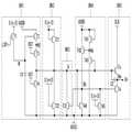
도 5는 본 발명의 제1 실시예에 따른 게이트 쉬프트 레지스터의 일 스테이지 구성을 보여준다. 그리고, 도 6은 라인 샘플링 신호(LSP), 글로벌 리셋 신호(RST), 글로벌 스타트 신호(VST) 및 클럭 신호(CLK)의 파형과, 그에 따른 노드 M 및 노드 Q의 전위와, 센싱용 게이트 펄스(P2n)의 출력 파형을 보여준다.5 shows a one-stage configuration of a gate shift register according to the first embodiment of the present invention. 6 shows waveforms of the line sampling signal LSP, the global reset signal RST, the global start signal VST and the clock signal CLK and the potentials of the node M and the node Q, (P2n).
제n 스테이지(STGn)는 도 5와 같이 제n-3 스테이지(STG(n-3)의 게이트 출력신호(S(n-3))(구체적으로, 화상 표시용 게이트 펄스)를 캐리 신호(CRY)로 입력 받을 수 있으나, 이에 한정되는 것은 아니다. 캐리 신호(CRY)는 전단 스테이지들 중 어느 하나로부터 입력 받을 수 있다. 도 5에서, 제1 라인 샘플링 펄스(L1)는 제n 픽셀 라인이 센싱될 수 있도록 제n 스테이지에 입력되는 캐리 신호(CRY)에 동기되고 있다. 제2 라인 샘플링 펄스(L2)는 수직 블랭크 기간(BP)에서 글로벌 스타트 신호(VST)에 동기된다. 글로벌 리셋 신호(RST)는 수직 블랭크 기간(BP)에서 글로벌 스타트 신호(VST)에 앞서 인가된다. 도 5의 스위치 T2와 스위치 T3의 사이즈를 최소화할 수 있도록, 글로벌 리셋 신호(RST)의 펄스폭(W2)은 글로벌 스타트 신호(VST)의 펄스폭(W1)에 비해 넓은 것이 바람직하다.The n-th stage STGn receives the gate output signal S (n-3) (specifically, the image display gate pulse) of the n-3th stage STG In FIG. 5, the first line sampling pulse (L1) is a signal that the n-th pixel line is connected to the sensing The second line sampling pulse L2 is synchronized with the global start signal VST in the vertical blanking period BP. The global reset signal RST (RST) is synchronized with the carry signal CRY input to the n- Is applied prior to the global start signal VST in the vertical blank period BP. The pulse width W2 of the global reset signal RST is set to the global Is preferably larger than the pulse width W1 of the start signal VST.
도 5 및 도 6을 참조하면, 특정 프레임에서 센싱용 게이트 펄스(P2n)를 출력하기 위해, 제n 스테이지(STGn)는 노드 Q에 연결된 샘플링부(BK1)와, 노드 Q 및 노드 Qb에 연결된 출력부(BK5)를 포함한다.5 and 6, in order to output the sensing gate pulse P2n in a specific frame, the n-th stage STGn includes a sampling section BK1 connected to the node Q and an output connected to the node Q and the node Qb (BK5).
출력부(BK5)는 노드 Q가 활성화되는 기간 내에서 화상 표시용 게이트 펄스(P1) 또는 상기 센싱용 게이트 펄스(P2)를 출력한다. 이를 위해, 출력부(BK5)는 풀업 트랜지스터 Tu와 풀다운 트랜지스터 Td와 커패시터 C2를 포함한다. 풀업 트랜지스터 Tu는 노드 Q에 연결된 게이트전극, 클럭 신호(CLK)가 인가되는 드레인전극, 및 노드 No에 연결된 소스전극을 가지며, 노드 Q가 활성화되는 기간 내에서 클럭 신호(CLK)가 입력될 때 이 클럭 신호(CLK)를 노드 No에 출력한다. 풀다운 트랜지스터 Td는 노드 Qb에 연결된 게이트전극, 노드 No에 연결된 드레인전극, 및 저전위 전원전압(GVSS)이 인가되는 소스전극을 가지며, 노드 Qb가 활성화되는 기간 동안 저전위 전원전압(GVSS)을 노드 No에 출력한다. 커패시터 C2는 노드 Q와 노드 No 사이에 접속되며, 노드 Q가 활성화되는 기간 내에서 클럭 신호(CLK)가 입력될 때 노드 Q의 전위를 부스팅함으로써 풀업 트랜지스터 Tu를 충분히 온 시킨다.The output section BK5 outputs the image display gate pulse P1 or the sensing gate pulse P2 within a period in which the node Q is activated. To this end, the output BK5 includes a pull-up transistor Tu, a pull-down transistor Td and a capacitor C2. The pull-up transistor Tu has a gate electrode connected to the node Q, a drain electrode to which a clock signal (CLK) is applied, and a source electrode connected to the node No. When the clock signal (CLK) And outputs the clock signal CLK to the node No. The pull-down transistor Td has a gate electrode connected to the node Qb, a drain electrode connected to the node No, and a source electrode to which a low potential power supply voltage (GVSS) is applied. The low potential power supply voltage (GVSS) No. Capacitor C2 is connected between node Q and node No and turns on pull-up transistor Tu sufficiently by boosting the potential of node Q when the clock signal CLK is input within the period in which node Q is active.
샘플링부(BK1)는 노드 Q를 활성화하기 위한 캐리 신호(CRY,S(n-3))에 동기 된 제1 라인 샘플링 펄스(L1)에 따라 화상 데이터 기입 기간(WP) 내에서 노드 M을 활성화하고, 이 노드 M의 활성 상태를 수직 블랭크 기간(BP)의 일정 시점까지 유지시킨다. 노드 M의 활성 전위는 도 6에서와 같이 제1 라인 샘플링 펄스(L1)가 인가되는 시점부터 제2 라인 샘플링 펄스(L2)가 인가되는 시점까지 유지된다. 샘플링부(BK1)는 수직 블랭크 기간(BP)에서, 자신에게 구비된 노드 M의 활성 전위와 글로벌 리셋 신호(RST)에 따라 노드 Q를 활성화한다. 이를 위해, 샘플링부(BK1)는 스위치 T1, 스위치 T2, 스위치 T3, 스위치 T4, 및 커패시터 C1를 포함한다.The sampling unit BK1 activates the node M in the image data writing period WP in accordance with the first line sampling pulse L1 synchronized with the carry signal CRY, S (n-3) , And maintains the active state of this node M until a certain point in the vertical blanking period (BP). The active potential of the node M is maintained from the application of the first line sampling pulse L1 to the application of the second line sampling pulse L2 as shown in FIG. The sampling unit BK1 activates the node Q in accordance with the active potential of the node M and the global reset signal RST provided thereto in the vertical blanking period BP. To this end, the sampling unit BK1 includes a switch T1, a switch T2, a switch T3, a switch T4, and a capacitor C1.
스위치 T1은 제1 라인 샘플링 펄스(L1)와 제2 라인 샘플링 펄스(L2)를 포함한 라인 샘플링 신호(LSP)가 인가되는 게이트전극, 캐리 신호(CRY)가 인가되는 드레인전극, 및 노드 M에 연결된 소스전극을 갖는다. 스위치 T1은 화상 데이터 기입 기간(WP)에서 제1 라인 샘플링 펄스(L1)에 동기되는 캐리 신호(CRY,S(n-3))를 노드 M에 저장하여 노드 M을 활성화시킨 후, 제2 라인 샘플링 펄스(L2)에 따라 수직 블랭크 기간(BP)의 일정 시점에서 노드 M을 비 활성화시킨다. 커패시터 C1은 노드 M과 저전위 전원전압(GVSS)의 입력단 사이에 연결되어 노드 M의 전위를 유지시킨다. 스위치 T2는 노드 M에 연결된 게이트전극, 고전위 전원전압(GVDD)이 인가되는 드레인전극, 및 노드 N1에 연결된 소스전극을 갖는다. 스위치 T2는 노드 M의 활성 전위에 따라 고전위 전원전압(GVDD)을 노드 N1에 인가한다. 스위치 T3는 글로벌 리셋 신호(RST)가 인가되는 게이트전극, 노드 N1에 연결된 드레인전극, 및 노드 Q에 연결된 소스전극을 갖는다. 스위치 T3는 수직 블랭크 기간(BP)에서 노드 N1에 충전된 고전위 전원전압(GVDD)을 글로벌 리셋 신호(RST)에 따라 노드 Q에 인가한다. 스위치 T4는 글로벌 스타트 신호(VST)가 인가되는 게이트전극, 노드 Q에 연결된 드레인전극, 및 저전위 전원전압(GVSS)이 인가되는 소스전극을 갖는다. 스위치 T4는 수직 블랭크 기간(BP)에서 글로벌 스타트 신호(VST)에 따라 노드 Q에 저전위 전원전압(GVSS)을 인가하여 노드 Q를 비 활성화시킨다.The switch T1 is connected to a gate electrode to which a line sampling signal LSP including a first line sampling pulse L1 and a second line sampling pulse L2 is applied, a drain electrode to which a carry signal CRY is applied, Source electrode. The switch T1 stores the carry signal (CRY, S (n-3)) synchronized with the first line sampling pulse L1 in the image data writing period WP to the node M to activate the node M, And deactivates the node M at a certain point in the vertical blanking period BP according to the sampling pulse L2. The capacitor C1 is connected between the node M and the input terminal of the low potential power supply voltage (GVSS) to maintain the potential of the node M. The switch T2 has a gate electrode connected to the node M, a drain electrode to which the high potential power supply voltage GVDD is applied, and a source electrode connected to the node N1. The switch T2 applies the high potential power supply voltage GVDD to the node N1 according to the active potential of the node M. [ Switch T3 has a gate electrode to which a global reset signal RST is applied, a drain electrode connected to node N1, and a source electrode connected to node Q. The switch T3 applies the high-potential power supply voltage GVDD charged in the node N1 in the vertical blanking period BP to the node Q in accordance with the global reset signal RST. The switch T4 has a gate electrode to which the global start signal VST is applied, a drain electrode connected to the node Q, and a source electrode to which the low potential supply voltage GVSS is applied. The switch T4 applies the low potential supply voltage GVSS to the node Q in accordance with the global start signal VST in the vertical blanking period BP to inactivate the node Q.
한편, 제n 스테이지(STGn)는 노드 Q에 연결된 입력부(BK2)와, 노드 Q 및 노드 Qb에 연결된 제1 안정화부(BK3)와 인버터부(BK4)를 더 포함할 수 있다.Meanwhile, the n-th stage STGn may further include an input unit BK2 connected to the node Q, a first stabilization unit BK3 connected to the node Q and the node Qb, and an inverter unit BK4.
입력부(BK2)는 화상 데이터 기입 기간(WP) 내에서 캐리 신호(CRY,S(n-3))를 노드 Q에 인가하여 노드 Q를 활성화시키는 스위치 T21과, 리셋 신호(S(n+3))에 따라 저전위 전원전압(GVSS)을 노드 Q에 인가하여 노드 Q를 비 활성화시키는 스위치 T22를 포함한다.The input section BK2 includes a switch T21 for applying the carry signal CRY, S (n-3) to the node Q to activate the node Q in the image data writing period WP and the reset signal S (n + And a switch T22 for applying a low potential supply voltage (GVSS) to the node Q to deactivate the node Q.
제1 안정화부(BK3)는 노드 Qb에 연결된 게이트전극, 노드 Q에 연결된 드레인전극 및 저전위 전원전압(GVSS)이 인가되는 소스전극을 가지며, 노드 Qb가 활성화될 때 노드 Q를 저전위 전원전압(GVSS)으로 비 활성화시키는 스위치 T31을 포함한다.The first stabilization unit BK3 has a gate electrode connected to the node Qb, a drain electrode connected to the node Q, and a source electrode to which the low potential power supply voltage GVSS is applied. When the node Qb is activated, Lt; RTI ID = 0.0 > (GVSS). ≪ / RTI >
인버터부(BK4)는 노드 Q의 전위와 노드 Qb의 전위가 상반되도록 하기 위해 스위치 T41, T42, T43, T44 및 T45를 포함한다. 스위치 T41은 고전위 전원전압(GVDD)이 인가되는 게이트전극과 드레인전극, 노드 Nx에 연결된 소스전극을 가지며, 노드 Nx를 고전위 전원전압(GVDD)으로 활성화 시킨다. 스위치 T42는 노드 Nx에 연결된 게이트전극, 고전위 전원전압(GVDD)이 인가되는 드레인전극, 노드 Qb에 연결되는 소스전극을 가지며, 노드 Nx가 활성화될 때 노드 Qb에 고전위 전원전압(GVDD)을 인가한다. 스위치 T43은 노드 Q에 연결된 게이트전극, 노드 Nx에 연결된 드레인전극 및 저전위 전원전압(GVSS)이 인가되는 소스전극을 가지며, 노드 Q가 활성화될 때 노드 Nx에 저전위 전원전압(GVSS)을 인가하여 노드 Nx를 비 활성화시킨다. 스위치 T44는 노드 Q에 연결된 게이트전극, 노드 Qb에 연결된 드레인전극, 및 저전위 전원전압(GVSS)이 인가되는 소스전극을 가지며, 노드 Q가 활성화될 때 노드 Qb를 저전위 전원전압(GVSS)으로 비 활성화 시킨다. 스위치 T45는 캐리 신호(CRY,S(n-3))가 인가되는 게이트전극, 노드 Qb에 연결된 드레인전극, 및 저전위 전원전압(GVSS)이 인가되는 소스전극을 가지며, 캐리 신호(CRY,S(n-3))가 인가될 때 노드 Qb를 저전위 전원전압(GVSS)으로 비 활성화 시킨다.The inverter unit BK4 includes switches T41, T42, T43, T44, and T45 to make the potential of the node Q and the potential of the node Qb opposite. The switch T41 has a gate electrode and a drain electrode to which the high potential supply voltage GVDD is applied, and a source electrode connected to the node Nx, and activates the node Nx to the high potential supply voltage GVDD. The switch T42 has a gate electrode connected to the node Nx, a drain electrode to which the high potential power supply voltage GVDD is applied, and a source electrode connected to the node Qb. When the node Nx is activated, a high potential power supply voltage (GVDD) . The switch T43 has a gate electrode connected to the node Q, a drain electrode connected to the node Nx, and a source electrode to which the low potential power supply voltage GVSS is applied, and the low potential power supply voltage GVSS is applied to the node Nx when the node Q is activated Thereby deactivating the node Nx. The switch T44 has a gate electrode connected to the node Q, a drain electrode connected to the node Qb, and a source electrode to which a low potential supply voltage (GVSS) is applied. When the node Q is activated, the node Qb is turned to the low potential supply voltage Deactivate. The switch T45 has a gate electrode to which the carry signal (CRY, S (n-3)) is applied, a drain electrode connected to the node Qb and a source electrode to which the low potential supply voltage GVSS is applied. (n-3)) is applied, node Qb is inactivated to the low potential power supply voltage GVSS.
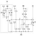
도 7 내지 도 11은 본 발명의 다른 실시예에 따른 게이트 쉬프트 레지스터의 일 스테이지 구성을 보여주는 도면들이다.7 to 11 are diagrams showing a one-stage configuration of a gate shift register according to another embodiment of the present invention.
도 5에 비해, 도 7의 게이트 쉬프트 레지스터는 동작의 안정성을 높이기 위해 샘플링부(BK1) 내에 스위치 T5,T6을 더 포함한다.Compared to Fig. 5, the gate shift register of Fig. 7 further includes switches T5 and T6 in the sampling section BK1 to enhance the stability of operation.
스위치 T5는 제1 라인 샘플링 펄스(L1)와 상기 제2 라인 샘플링 펄스(L2)가 인가되는 게이트전극, 스위치 T1의 소스전극과 노드 M 사이의 노드 N2에 연결된 드레인전극, 및 노드 M에 연결된 소스전극을 갖는다. 스위치 T5는 노드 M에 충전된 캐리 신호(CRY,S(n-3))가 누설되는 것을 방지한다. 스위치 T6은 노드 M에 연결된 게이트전극, 고전위 전원전압(GVDD)이 인가되는 드레인전극, 및 노드 N2에 연결된 소스전극을 갖는다. 스위치 T6는 노드 M에 캐리 신호(CRY,S(n-3))가 빠르게 충전되게 한다.The switch T5 includes a first line sampling pulse L1 and a gate electrode to which the second line sampling pulse L2 is applied, a drain electrode connected to the node N2 between the source electrode of the switch T1 and the node M, Electrode. The switch T5 prevents the carry signal (CRY, S (n-3)) charged in the node M from leaking. The switch T6 has a gate electrode connected to the node M, a drain electrode to which the high potential power supply voltage GVDD is applied, and a source electrode connected to the node N2. The switch T6 causes the node M to quickly charge the carry signal (CRY, S (n-3)).
도 5에 비해, 도 8의 게이트 쉬프트 레지스터는 동작의 안정성을 더욱 높이기 위해 제2 안정화부(BK6)를 더 포함한다.Compared to FIG. 5, the gate shift register of FIG. 8 further includes a second stabilization unit BK6 for further increasing the stability of operation.
제2 안정화부(BK6)는 스위치 T51과 스위치 T52를 포함하여, 노드 M이 활성화된 스테이지의 Qb 노드를 수직 브랭크 기간(BP)에서 저전위 전원전압(GVSS)으로 비 활성화시킴으로써 동작의 안전성을 더욱 높인다. 스위치 T51은 글로벌 리셋 신호(RST)가 인가되는 게이트전극, Qb 노드에 연결된 드레인전극, 및 노드 N3에 연결된 소스전극을 갖는다. 스위치 T52는 노드 M에 연결된 게이트전극, 노드 N3에 연결된 드레인전극, 및 상기 저전위 전원전압(GVSS)이 인가되는 소스전극을 갖는다.The second stabilizing unit BK6 includes the switch T51 and the switch T52 to inactivate the Qb node of the stage where the node M is activated from the vertical blanking period BP to the low potential supply voltage GVSS, Lt; / RTI > The switch T51 has a gate electrode to which a global reset signal RST is applied, a drain electrode connected to the Qb node, and a source electrode connected to the node N3. The switch T52 has a gate electrode connected to the node M, a drain electrode connected to the node N3, and a source electrode to which the low potential power supply voltage (GVSS) is applied.
도 5에 비해, 도 9의 게이트 쉬프트 레지스터는 스위치 T2의 드레인전극에 고전위 전원전압(GVDD) 대신에 클럭 신호(CLK)를 인가한다. 스위치 T2의 드레인전극에 클럭 신호(CLK)를 인가하면, 고전위 전원전압(GVDD)을 인가할 때에 비해 스위치 T2에서 누설되는 전류량이 줄어드는 효과가 있다.5, the gate shift register of FIG. 9 applies the clock signal CLK to the drain electrode of the switch T2 instead of the high-potential power supply voltage GVDD. When the clock signal CLK is applied to the drain electrode of the switch T2, the amount of current leaked from the switch T2 is reduced compared to when the high-potential power supply voltage GVDD is applied.
도 9에 비해, 도 10의 게이트 쉬프트 레지스터는 동작의 안정성을 높이기 위해 샘플링부(BK1) 내에 스위치 T5,T6을 더 포함한다. 도 10의 스위치 T5,T6은 도 7에서 설명한 것과 실질적으로 동일하다.Compared to FIG. 9, the gate shift register of FIG. 10 further includes switches T5 and T6 in the sampling section BK1 to enhance the stability of operation. The switches T5 and T6 in Fig. 10 are substantially the same as those described in Fig.
도 9에 비해, 도 11의 게이트 쉬프트 레지스터는 동작의 안정성을 더욱 높이기 위해 제2 안정화부(BK6)를 더 포함한다. 도 11의 제2 안정화부(BK6)는 도 8에서 설명한 것과 실질적으로 동일하다.Compared to FIG. 9, the gate shift register of FIG. 11 further includes a second stabilization unit BK6 for further increasing the stability of operation. The second stabilization unit BK6 of Fig. 11 is substantially the same as that described in Fig.
도 12는 라인 샘플링 신호(LSP)에 따라, 수평 블랭크 기간들(BP)에서 센싱용 게이트펄스(P27,P25)가 랜덤한 순서로 출력되는 일 예를 보여준다.Fig. 12 shows an example in which the gate pulse P27, P25 for sensing in the horizontal blank periods BP are output in a random order in accordance with the line sampling signal LSP.
도 12에서 센싱용 게이트펄스(P27,P25)가 출력되는 타이밍은, 도 5 내지 도 11에서 예시한 바와 같이 제n 스테이지(STGn)가 제n-3 스테이지(STG(n-3)의 게이트 출력신호(S(n-3), P1n-3)를 캐리 신호(CRY)로 입력 받는 것을 가정한 결과이다.The timing at which the sensing gate pulses P27 and P25 are output in Fig. 12 is such that the n-th stage STGn is the gate output of the n-3 stage STG (n-3) as shown in Figs. 5 to 11, And the signals S (n-3) and P1n-3 are received as the carry signal CRY.
제1 프레임에서 제1 라인 샘플링 펄스(L1)가 제7 스테이지에 입력되는 캐리 신호(S4)에 동기되는 경우, 제7 스테이지만이 제1 프레임의 수직 블랭크 기간(BP)에서 센싱용 게이트 펄스(P27)를 출력하고, 나머지 스테이지들은 제1 프레임의 수직 블랭크 기간(BP)에서 센싱용 게이트 펄스(P27)를 출력하지 못한다.In the first frame, when the first line sampling pulse L1 is synchronized with the carry signal S4 input to the seventh stage, only the seventh stage outputs the gate pulse for sensing (in the vertical blanking period BP of the first frame P27, and the remaining stages do not output the gate pulse P27 for sensing in the vertical blanking period BP of the first frame.
한편, 제2 프레임에서 제1 라인 샘플링 펄스(L1)가 제5 스테이지에 입력되는 캐리 신호(S2)에 동기되는 경우, 제5 스테이지만이 제2 프레임의 수직 블랭크 기간(BP)에서 센싱용 게이트 펄스(P25)를 출력하고, 나머지 스테이지들은 제2 프레임의 수직 블랭크 기간(BP)에서 센싱용 게이트 펄스(P27)를 출력하지 못한다.On the other hand, in the second frame, when the first line sampling pulse L1 is synchronized with the carry signal S2 input to the fifth stage, only the fifth stage is driven in the vertical blank period BP of the second frame, And outputs the pulse P25, and the remaining stages do not output the gate pulse P27 for sensing in the vertical blanking period BP of the second frame.
도 13은 본 발명의 실시예에 따른 게이트 쉬프트 레지스터를 포함한 유기발광 표시장치를 보여준다.13 illustrates an organic light emitting display including a gate shift register according to an embodiment of the present invention.
도 13을 참조하면, 본 발명의 유기발광 표시장치는 표시패널(100), 데이터 구동회로, 스캔 구동회로, 및 타이밍 콘트롤러(110) 등을 구비한다.Referring to FIG. 13, the OLED display of the present invention includes a
표시패널(100)에는 다수의 데이터라인들 및 센싱라인들과, 다수의 게이트라인들이 교차되고, 이 교차영역마다 외부 보상용 픽셀들이 매트릭스 형태로 배치되어 외부 보상용 픽셀 어레이를 구성할 수 있다. 각 픽셀은 OLED, 구동 TFT(Thin Film Transistor), 스토리지 커패시터, 제1 스위치 TFT, 및 제2 스위치 TFT를 포함할 수 있다. TFT들은 P 타입으로 구현되거나 또는, N 타입으로 구현되거나 또는, P 타입과 N 타입이 혼용된 하이브리드 타입으로 구현될 수 있다. 또한, TFT의 반도체층은, 아몰포스 실리콘 또는, 폴리 실리콘 또는, 산화물을 포함할 수 있다.In the
외부 보상용 픽셀 어레이를 갖는 본 발명의 유기발광 표시장치는 OLED와 구동 TFT의 전기적 특성을 센싱하고 그 센싱값에 따라 화상 표시용 데이터를 보정하는 기술이다. OLED의 전기적 특성은 OLED의 동작점 전압을 의미한다. 구동 TFT의 전기적 특성은 구동 TFT의 문턱전압과 구동 TFT의 전자 이동도를 의미한다.The organic light emitting display device having the pixel array for external compensation is a technique for sensing the electrical characteristics of the OLED and the driving TFT and correcting the image display data according to the sensing value. The electrical characteristics of the OLED refer to the operating point voltage of the OLED. The electrical characteristics of the driving TFT mean the threshold voltage of the driving TFT and the electron mobility of the driving TFT.
외부 보상용 픽셀 어레이를 포함한 유기발광 표시장치는 본원 출원인에 의해 기출원된 출원번호 제10-2013-0134256호(2013/11/06), 출원번호 제10-2013-0141334호(2013/11/20), 출원번호 제10-2013-0149395호(2013/12/03), 출원번호 제10-2014-0086901호(2014/07/10), 출원번호 제10-2014-0079255호(2014/06/26), 출원번호 제10-2014-0079587호(2014/06/27), 출원번호 제10-2014-0119357호(2014/09/05) 등에 나타나 있다.An organic light emitting display device including an external compensation pixel array is disclosed in Japanese Patent Application No. 10-2013-0134256 (2013/11/06), Application No. 10-2013-0141334 (2013/11 / 20), Application No. 10-2013-0149395 (2013/12/03), Application No. 10-2014-0086901 (2014/07/10), Application No. 10-2014-0079255 (2014/06 / 26), Application No. 10-2014-0079587 (2014/06/27), Application No. 10-2014-0119357 (2014/09/05), etc.
본 발명의 유기발광 표시장치는 픽셀들의 전기적 특성을 센싱하기 위해 실시간 센싱 프로세스를 수행한다. 본 발명의 유기발광 표시장치는 1 프레임 중에서 화상 데이터 기입 기간(WP)을 제외한 수직 블랭크 기간(BP)에서 센싱 동작을 수행하되, 1 프레임마다 1 픽셀라인씩 센싱한다. 여기서, 픽셀라인은 수평으로 이웃한 픽셀들의 집합을 의미하며, 1 픽셀라인에는 수평 해상도만큼의 픽셀들이 위치한다. 패널 구동회로는 화상 데이터 기입 기간(WP) 동안 화상 표시용 게이트펄스를 표시패널의 게이트라인들에 순차적으로 공급하여 화상 표시용 데이터를 표시패널의 모든 픽셀들에 기입하고, 수직 블랭크 기간(BP)에서 특정 픽셀라인에 연결된 게이트라인에만 센싱용 게이트펄스를 공급하여 센싱용 데이터를 상기 특정 픽셀라인의 픽셀들에 인가한다.The organic light emitting display of the present invention performs a real time sensing process to sense electrical characteristics of pixels. The organic light emitting display device of the present invention performs a sensing operation in one vertical blanking period (BP) excluding the image data writing period (WP) in one frame, and senses one pixel line per one frame. Here, the pixel line means a set of horizontally neighboring pixels, and one pixel line includes pixels as many as the horizontal resolution. The panel drive circuit sequentially supplies the image display gate pulse to the gate lines of the display panel during the image data writing period WP to write the image display data to all the pixels of the display panel, A gate pulse for sensing is applied only to a gate line connected to a specific pixel line to apply the sensing data to the pixels of the specific pixel line.
이를 위해, 데이터 구동회로는 다수의 소스 드라이브 IC들(120)을 포함한다. 소스 드라이브 IC들(120)은 타이밍 콘트롤러(110)로부터 화상 표시용 데이터들(RGB)을 입력 받는다. 소스 드라이브 IC들(120)은 타이밍 콘트롤러(110)로부터의 소스 타이밍 제어신호에 응답하여 화상 표시용 데이터들(RGB)을 감마보상전압으로 변환하여 데이터전압을 발생하고, 그 데이터전압을 화상 표시용 게이트펄스들에 동기되도록 표시패널(100)의 데이터라인들에 공급한다. 소스 드라이브 IC들은 COG(Chip On Glass) 공정이나 TAB(Tape Automated Bonding) 공정으로 표시패널(100)의 데이터라인들에 접속될 수 있다.To this end, the data drive circuit includes a plurality of source drive
스캔 구동회로는 타이밍 콘트롤러(110)와 표시패널(100)의 게이트라인들 사이에 접속된 레벨 쉬프터(level shiftet)(150), 및 게이트 쉬프트 레지스터(130)를 구비한다.The scan driver circuit includes a
레벨 쉬프터(150)는 타이밍 콘트롤러(110)로부터 입력되는 클럭 신호들(CLKs)의 TTL(Transistor-Transistor- Logic) 레벨 전압을 표시패널(100)에 형성된 TFT를 스위칭시킬 수 있는 게이트 하이 전압과 게이트 로우 전압으로 레벨 쉬프팅한다. 게이트 쉬프트 레지스터(130)는 도 3 내지 도 12를 통해 설명한 바와 같이 종래 대비 간소화 스테이지 구성만으로 수평 블랭크 기간에 센싱용 게이트펄스를 랜덤한 순서로 출력함으로써, 센싱 대상 픽셀라인을 불규칙하게 선택할 수 있다.The
스캔 구동회로는 GIP(Gate In Panel) 방식으로 표시패널(100)의 하부 기판 상에 직접 형성될 수 있다. GIP 방식에서, 레벨 쉬프터(150)는 PCB(140) 상에 실장되고, 게이트 쉬프트 레지스터(130)는 표시패널(100)의 하부기판 상에 형성될 수 있다. 게이트 쉬프트 레지스터(130)는 표시패널(100)에서 화상이 표시되지 않는 영역(즉, 베젤 영역(BZ))에 형성된다.The scan driver circuit may be formed directly on the lower substrate of the
타이밍 콘트롤러(110)는 공지의 다양한 인터페이스 방식을 통해 외부의 호스트 시스템로부터 화상 표시용 데이터(RGB)를 입력 받는다. 타이밍 콘트롤러(110)는 실시간 센싱에 따른 센싱 결과를 기초로 픽셀들의 전기적 특성 편차가 보상되도록 화상 표시용 데이터(RGB)를 보정한 후 소스 드라이브 IC들(120)로 전송할 수 있다.The
타이밍 콘트롤러(110)는 호스트 시스템으로부터 수직 동기신호(Vsync), 수평 동기신호(Hsync), 데이터 인에이블 신호(Data Enable, DE), 메인 클럭(MCLK) 등의 타이밍신호를 입력 받는다. 타이밍 콘트롤러(110)는 호스트 시스템으로부터의 타이밍 신호를 기준으로 데이터 구동회로 동작 타이밍을 제어하기 위한 데이터 타이밍 제어신호와, 스캔 구동회로의 동작 타이밍을 제어하기 위한 스캔 타이밍 제어신호를 생성한다.The
스캔 타이밍 제어신호는 라인 샘플링 신호(LSP), 글로벌 리셋 신호(RST), 글로벌 스타트 신호(VST) 및 클럭 신호(CLKs) 등을 포함한다.The scan timing control signal includes a line sampling signal LSP, a global reset signal RST, a global start signal VST and a clock signal CLKs.
데이터 타이밍 제어신호는 소스 샘플링 클럭(Source Sampling Clock, SSC), 소스 출력 인에이블신호(Source Output Enable, SOE) 등을 포함한다. 소스 샘플링 클럭(SSC)은 라이징 또는 폴링 에지에 기준하여 소스 드라이브 IC들(120) 내에서 데이터의 샘플링 타이밍을 제어하는 클럭신호이다. 소스 출력 인에이블신호(SOE)는 데이터전압의 출력 타이밍을 제어하는 신호이다.The data timing control signal includes a source sampling clock (SSC), a source output enable signal (SOE), and the like. The source sampling clock SSC is a clock signal that controls the sampling timing of data in the source drive
전술한 본 발명은 다음과 같은 효과가 있다.The above-described present invention has the following effects.
첫째, 본 발명은 실시간 센싱을 구현하기 위한 게이트 쉬프트 레지스터의 구성이 종래 대비 매우 간소하다. 그럼에도 불구하고, 본 발명은 수평 블랭크 기간에서 센싱용 게이트펄스를 랜덤한 순서로 출력함으로써, 센싱 대상 픽셀라인을 불규칙하게 선택할 수 있다. 본 발명은 센싱 대상 픽셀라인을 불규칙하게 선택함으로써 종래 기술의 문제점인 순차 센싱에 따른 휘도 편차 시인 현상을 방지할 수 있다.First, the structure of the gate shift register for real-time sensing is very simple compared to the conventional one. Nevertheless, the present invention can randomly select the pixel line to be sensed by outputting the sensing gate pulse in a random order in the horizontal blanking period. The present invention can prevent the phenomenon of luminance deviation due to sequential sensing, which is a problem of the related art, by irregularly selecting the pixel line to be sensed.
둘째, 본 발명은 종래 대비 간소한 구성의 게이트 쉬프트 레지스터를 구비하기 때문에 공정 불량이 발생될 확률이 낮고, 동작의 신뢰성이 높다.Second, since the present invention includes a gate shift register having a simple configuration, the probability of occurrence of a process failure is low and the reliability of operation is high.
셋째, 본 발명의 게이트 쉬프트 레지스터는 그 구성이 간소하기 때문에 표시패널에 내장될 경우 베젤 사이즈를 감소시킬 수 있다. 그리고, 본 발명의 게이트 쉬프트 레지스터는 실시간 센싱을 위해 클럭 라인 및 전원 라인을 추가할 필요가 없기 때문에 종래 대비 소비 전력 면에서 유리하다.Third, since the gate shift register of the present invention has a simple structure, the bezel size can be reduced when the gate shift register is embedded in a display panel. The gate shift register of the present invention is advantageous in terms of power consumption compared to the conventional one because it is unnecessary to add a clock line and a power supply line for real time sensing.
이상 설명한 내용을 통해 당업자라면 본 발명의 기술사상을 일탈하지 아니하는 범위에서 다양한 변경 및 수정이 가능함을 알 수 있을 것이다. 따라서, 본 발명의 기술적 범위는 명세서의 상세한 설명에 기재된 내용으로 한정되는 것이 아니라 특허 청구의 범위에 의해 정하여져야만 할 것이다.It will be apparent to those skilled in the art that various modifications and variations can be made in the present invention without departing from the spirit or scope of the invention. Therefore, the technical scope of the present invention should not be limited to the contents described in the detailed description of the specification, but should be defined by the claims.
100 : 표시패널110 : 타이밍 콘트롤러
120 : 소스 드라이브 IC130 : 게이트 쉬프트 레지스터
140 : PCB150 : 레벨 쉬프터100: display panel 110: timing controller
120: Source drive IC 130: Gate shift register
140: PCB 150: Level shifter
Claims (15)
Translated fromKorean상기 스테이지들 각각은,
상기 수직 블랭크 기간(BP)에서, 자신에게 구비된 노드 M의 활성 전위와 상기 스테이지들에 공통으로 인가되는 글로벌 리셋 신호(RST)에 따라 노드 Q를 활성화하는 샘플링부(BK1); 및
상기 수빅 블랭크 기간(BP)에서 상기 노드 Q가 활성화되는 기간 동안 상기 센싱용 게이트 펄스(P2)를 출력하는 출력부(BK5)를 포함하고,
상기 노드 M은 상기 노드 Q를 활성화하기 위한 캐리 신호(CRY)에 동기 된 제1 라인 샘플링 펄스(L1)에 따라 상기 화상 데이터 기입 기간(WP) 내에서 활성화되는 게이트 쉬프트 레지스터.And outputs the image display gate pulses P1 during the image data writing period WP during one frame and outputs the gate pulse P2 for sensing in the vertical blank period BP during which the image display data is not written in the one frame A gate shift register having a plurality of stages,
Each of the stages includes:
A sampling unit BK1 for activating the node Q in accordance with the active potential of the node M included in the vertical blanking period BP and the global reset signal RST commonly applied to the stages; And
And an output unit (BK5) for outputting the sensing gate pulse (P2) during a period in which the node (Q) is activated in the sub-blank period (BP)
Wherein the node M is activated in the image data writing period (WP) according to a first line sampling pulse (L1) synchronized with a carry signal (CRY) for activating the node (Q).
상기 수직 블랭크 기간(BP) 내에서,
상기 노드 Q는 상기 글로벌 리셋 신호(RST)에 이어 상기 스테이지들에 공통으로 인가되는 글로벌 스타트 신호(VST)에 따라 비 활성화되고,
상기 노드 M은 상기 글로벌 스타트 신호(VST)에 동기되는 제2 라인 샘플링 펄스(L2)에 따라 비 활성화되는 게이트 쉬프트 레지스터.The method according to claim 1,
Within the vertical blanking period (BP)
The node Q is deactivated according to the global start signal VST commonly applied to the stages following the global reset signal RST,
And the node M is inactivated according to a second line sampling pulse (L2) synchronized with the global start signal (VST).
상기 노드 M의 활성 전위는 상기 제1 라인 샘플링 펄스(L1)가 인가되는 시점부터 상기 제2 라인 샘플링 펄스(L2)가 인가되는 시점까지 유지되는 게이트 쉬프트 레지스터.3. The method of claim 2,
And an active potential of the node M is maintained from a time point when the first line sampling pulse (L1) is applied to a time point when the second line sampling pulse (L2) is applied.
상기 제1 라인 샘플링 펄스(L1)는 차등 간격으로 인가되고, 상기 제2 라인 샘플링 펄스(L2)는 균등 간격으로 인가되는 게이트 쉬프터 레지스터.3. The method of claim 2,
Wherein the first line sampling pulse (L1) is applied at a differential interval, and the second line sampling pulse (L2) is applied at an even interval.
상기 글로벌 리셋 신호(RST)의 펄스폭은 상기 글로벌 스타트 신호(VST)의 펄스폭에 비해 넓은 게이트 쉬프트 레지스터.3. The method of claim 2,
The pulse width of the global reset signal RST is larger than the pulse width of the global start signal VST.
상기 샘플링부(BK1)는,
상기 제1 라인 샘플링 펄스(L1)와 상기 제2 라인 샘플링 펄스(L2)가 인가되는 게이트전극, 상기 캐리 신호(CRY)가 인가되는 드레인전극, 및 상기 노드 M에 연결된 소스전극을 갖는 스위치 T1과,
상기 노드 M에 연결된 게이트전극, 고전위 전원전압(GVDD)이 인가되는 드레인전극, 및 노드 N1에 연결된 소스전극을 갖는 스위치 T2와,
상기 글로벌 리셋 신호(RST)가 인가되는 게이트전극, 상기 노드 N1에 연결된 드레인전극, 및 상기 노드 Q에 연결된 소스전극을 갖는 스위치 T3과,
상기 글로벌 스타트 신호(VST)가 인가되는 게이트전극, 상기 노드 Q에 연결된 드레인전극, 및 저전위 전원전압(GVSS)이 인가되는 소스전극을 갖는 스위치 T4와,
상기 노드 M과 상기 저전위 전원전압(GVSS)의 입력단 사이에 연결되는 커패시터 C1을 포함하는 게이트 쉬프트 레지스터.3. The method of claim 2,
The sampling unit (BK1)
A switch T1 having a gate electrode to which the first line sampling pulse L1 and the second line sampling pulse L2 are applied, a drain electrode to which the carry signal CRY is applied, and a source electrode connected to the node M, ,
A switch T2 having a gate electrode connected to the node M, a drain electrode to which a high potential power supply voltage (GVDD) is applied, and a source electrode connected to the node N1,
A switch T3 having a gate electrode to which the global reset signal RST is applied, a drain electrode connected to the node N1, and a source electrode connected to the node Q,
A switch T4 having a gate electrode to which the global start signal VST is applied, a drain electrode connected to the node Q, and a source electrode to which a low potential power supply voltage GVSS is applied,
And a capacitor C1 connected between the node M and the input terminal of the low potential power supply voltage (GVSS).
상기 샘플링부(BK1)는,
상기 제1 라인 샘플링 펄스(L1)와 상기 제2 라인 샘플링 펄스(L2)가 인가되는 게이트전극, 상기 캐리 신호(CRY)가 인가되는 드레인전극, 및 상기 노드 M에 연결된 소스전극을 갖는 스위치 T1과,
상기 노드 M에 연결된 게이트전극, 상기 클럭 신호(CLK)가 인가되는 드레인전극, 및 노드 N1에 연결된 소스전극을 갖는 스위치 T2와,
상기 글로벌 리셋 신호(RST)가 인가되는 게이트전극, 상기 노드 N1에 연결된 드레인전극, 및 상기 노드 Q에 연결된 소스전극을 갖는 스위치 T3과,
상기 글로벌 스타트 신호(VST)가 인가되는 게이트전극, 상기 노드 Q에 연결된 드레인전극, 및 저전위 전원전압(GVSS)이 인가되는 소스전극을 갖는 스위치 T4와,
상기 노드 M과 상기 저전위 전원전압(GVSS)의 입력단 사이에 연결되는 커패시터 C1을 포함하는 게이트 쉬프트 레지스터.3. The method of claim 2,
The sampling unit (BK1)
A switch T1 having a gate electrode to which the first line sampling pulse L1 and the second line sampling pulse L2 are applied, a drain electrode to which the carry signal CRY is applied, and a source electrode connected to the node M, ,
A switch T2 having a gate electrode connected to the node M, a drain electrode to which the clock signal CLK is applied, and a source electrode connected to the node N1,
A switch T3 having a gate electrode to which the global reset signal RST is applied, a drain electrode connected to the node N1, and a source electrode connected to the node Q,
A switch T4 having a gate electrode to which the global start signal VST is applied, a drain electrode connected to the node Q, and a source electrode to which a low potential power supply voltage GVSS is applied,
And a capacitor C1 connected between the node M and the input terminal of the low potential power supply voltage (GVSS).
상기 샘플링부(BK1)는,
상기 제1 라인 샘플링 펄스(L1)와 상기 제2 라인 샘플링 펄스(L2)가 인가되는 게이트전극, 상기 스위치 T1의 소스전극과 상기 노드 M 사이의 노드 N2에 연결된 드레인전극, 및 상기 노드 M에 연결된 소스전극을 갖는 스위치 T5와,
상기 노드 M에 연결된 게이트전극, 상기 고전위 전원전압(GVDD)이 인가되는 드레인전극, 및 상기 노드 N2에 연결된 소스전극을 갖는 스위치 T6을 더 포함하는 게이트 쉬프트 레지스터.8. The method according to claim 6 or 7,
The sampling unit (BK1)
A gate electrode to which the first line sampling pulse L1 and the second line sampling pulse L2 are applied, a drain electrode connected to a node N2 between the source electrode of the switch T1 and the node M, A switch T5 having a source electrode,
A switch T6 having a gate electrode coupled to the node M, a drain electrode to which the high potential power supply voltage GVDD is applied, and a source electrode coupled to the node N2.
상기 노드 Q가 활성화되는 기간 동안 비 활성화되는 노드 Qb와 상기 저전위 전원전압(GVSS)의 입력단 사이에 연결된 안정화부(BK6)를 더 포함하고,
상기 안정화부(BK6)는
상기 글로벌 리셋 신호(RST)가 인가되는 게이트전극, 상기 Qb 노드에 연결된 드레인전극, 및 노드 N3에 연결된 소스전극을 갖는 스위치 T51과,
상기 노드 M에 연결된 게이트전극, 상기 노드 N3에 연결된 드레인전극, 및 상기 저전위 전원전압(GVSS)이 인가되는 소스전극을 갖는 스위치 T52를 포함하는 게이트 쉬프트 레지스터.9. The method of claim 8,
Further comprising a stabilization unit (BK6) connected between an inactive node (Qb) during an active period of the node (Q) and an input terminal of the low potential power supply voltage (GVSS)
The stabilizing unit BK6
A switch T51 having a gate electrode to which the global reset signal RST is applied, a drain electrode connected to the Qb node, and a source electrode connected to the node N3,
And a switch T52 having a gate electrode connected to the node M, a drain electrode connected to the node N3, and a source electrode to which the low potential power supply voltage (GVSS) is applied.
1 프레임 중의 화상 데이터 기입 기간(WP) 동안 화상 표시용 게이트 펄스들(P1)을 상기 게이트라인들에 출력하고, 상기 1 프레임 중에서 상기 화상 표시용 데이터가 기입되지 않는 수직 블랭크 기간(BP)에서 센싱용 게이트 펄스(P2)를 상기 게이트라인들에 선택적으로 출력하는 다수의 스테이지들을 갖는 게이트 쉬프트 레지스터를 구비하고,
상기 스테이지들 각각은, 상기 수직 블랭크 기간(BP)에서, 자신에게 구비된 노드 M의 활성 전위와 상기 스테이지들에 공통으로 인가되는 글로벌 리셋 신호(RST)에 따라 노드 Q를 활성화하는 샘플링부(BK1); 및
상기 수직 블랭크 기간(BP)에서 상기 노드 Q가 활성화되는 기간 동안 상기 센싱용 게이트 펄스(P2)를 출력하는 출력부(BK5)
를 포함하고,
상기 노드 M은 상기 노드 Q를 활성화하기 위한 캐리 신호(CRY)에 동기 된 제1 라인 샘플링 펄스(L1)에 따라 상기 화상 데이터 기입 기간(WP) 내에서 활성화되는 유기발광 표시장치.
A display panel having gate lines; And
And outputs image display gate pulses P1 to the gate lines during the image data writing period WP during one frame and outputs the gate pulses P1 to the gate lines in the vertical blanking period BP during which the image display data is not written And a gate shift register having a plurality of stages for selectively outputting gate pulses P2 to the gate lines,
Each of the stages includes a sampling unit BK1 for activating a node Q in accordance with a global reset signal RST applied commonly to the stages and an active potential of a node M included in the vertical blanking period BP, ); And
An output unit BK5 for outputting the sensing gate pulse P2 during the period in which the node Q is activated in the vertical blanking period BP,
Lt; / RTI >
The node M is activated in the image data writing period (WP) in accordance with a first line sampling pulse (L1) synchronized with a carry signal (CRY) for activating the node (Q).
상기 스테이지들 중 어느 하나의 특정 스테이지를 통해 상기 센싱용 게이트 펄스(P2)를 출력하는 단계는,
상기 수직 블랭크 기간(BP)에서, 상기 특정 스테이지에 구비된 노드 M의 활성 전위와 상기 스테이지들에 공통으로 인가되는 글로벌 리셋 신호(RST)에 따라 상기 특정 스테이지의 노드 Q를 활성화하는 단계; 및
상기 수빅 블랭크 기간(BP)에서 상기 노드 Q가 활성화되는 기간 동안 상기 센싱용 게이트 펄스(P2)를 출력하는 단계를 포함하고,
상기 노드 M은 상기 노드 Q를 활성화하기 위한 캐리 신호(CRY)에 동기 된 제1 라인 샘플링 펄스(L1)에 따라 상기 화상 데이터 기입 기간(WP) 내에서 활성화되는 유기발광 표시장치의 구동방법.The image display gate pulse P1 is outputted to the gate lines of the display panel during the image data writing period WP during one frame including a plurality of stages and the image display data is not written in the one frame And selectively outputting a sensing gate pulse (P2) to the gate lines in a vertical blank period (BP)
The step of outputting the sensing gate pulse (P2) through any one of the stages,
Activating a node Q of the particular stage in accordance with an active potential of a node M provided in the specific stage and a global reset signal RST commonly applied to the stages in the vertical blanking period BP; And
And outputting the sensing gate pulse (P2) during a period in which the node (Q) is activated in the sub-blank period (BP)
Wherein the node M is activated in the image data writing period (WP) according to a first line sampling pulse (L1) synchronized with a carry signal (CRY) for activating the node (Q).
상기 수직 블랭크 기간(BP) 내에서,
상기 노드 Q는 상기 글로벌 리셋 신호(RST)에 이어 상기 스테이지들에 공통으로 인가되는 글로벌 스타트 신호(VST)에 따라 비 활성화되고,
상기 노드 M은 상기 글로벌 스타트 신호(VST)에 동기되는 제2 라인 샘플링 펄스(L2)에 따라 비 활성화되는 유기발광 표시장치의 구동방법.12. The method of claim 11,
Within the vertical blanking period (BP)
The node Q is deactivated according to the global start signal VST commonly applied to the stages following the global reset signal RST,
And the node M is inactivated according to a second line sampling pulse (L2) synchronized with the global start signal (VST).
상기 노드 M의 활성 전위는 상기 제1 라인 샘플링 펄스(L1)가 인가되는 시점부터 상기 제2 라인 샘플링 펄스(L2)가 인가되는 시점까지 유지되는 유기발광 표시장치의 구동방법.13. The method of claim 12,
Wherein the active potential of the node M is maintained from the application of the first line sampling pulse (L1) to the application of the second line sampling pulse (L2).
상기 제1 라인 샘플링 펄스(L1)는 차등 간격으로 인가되고, 상기 제2 라인 샘플링 펄스(L2)는 균등 간격으로 인가되는 유기발광 표시장치의 구동방법.13. The method of claim 12,
Wherein the first line sampling pulse (L1) is applied at a differential interval, and the second line sampling pulse (L2) is applied at an even interval.
상기 글로벌 리셋 신호(RST)의 펄스폭은 상기 글로벌 스타트 신호(VST)의 펄스폭에 비해 넓은 유기발광 표시장치의 구동방법.13. The method of claim 12,
Wherein a pulse width of the global reset signal RST is larger than a pulse width of the global start signal VST.
Priority Applications (2)
| Application Number | Priority Date | Filing Date | Title |
|---|---|---|---|
| KR1020150188925AKR102635475B1 (en) | 2015-12-29 | 2015-12-29 | Gate shift register and organic light emitting display device including the same, and driving method of the same |
| KR1020240017228AKR20240023407A (en) | 2015-12-29 | 2024-02-05 | Gate shift register and organic light emitting display device including the same, and driving method of the same |
Applications Claiming Priority (1)
| Application Number | Priority Date | Filing Date | Title |
|---|---|---|---|
| KR1020150188925AKR102635475B1 (en) | 2015-12-29 | 2015-12-29 | Gate shift register and organic light emitting display device including the same, and driving method of the same |
Related Child Applications (1)
| Application Number | Title | Priority Date | Filing Date |
|---|---|---|---|
| KR1020240017228ADivisionKR20240023407A (en) | 2015-12-29 | 2024-02-05 | Gate shift register and organic light emitting display device including the same, and driving method of the same |
Publications (2)
| Publication Number | Publication Date |
|---|---|
| KR20170078978Atrue KR20170078978A (en) | 2017-07-10 |
| KR102635475B1 KR102635475B1 (en) | 2024-02-08 |
Family
ID=59355142
Family Applications (2)
| Application Number | Title | Priority Date | Filing Date |
|---|---|---|---|
| KR1020150188925AActiveKR102635475B1 (en) | 2015-12-29 | 2015-12-29 | Gate shift register and organic light emitting display device including the same, and driving method of the same |
| KR1020240017228APendingKR20240023407A (en) | 2015-12-29 | 2024-02-05 | Gate shift register and organic light emitting display device including the same, and driving method of the same |
Family Applications After (1)
| Application Number | Title | Priority Date | Filing Date |
|---|---|---|---|
| KR1020240017228APendingKR20240023407A (en) | 2015-12-29 | 2024-02-05 | Gate shift register and organic light emitting display device including the same, and driving method of the same |
Country Status (1)
| Country | Link |
|---|---|
| KR (2) | KR102635475B1 (en) |
Cited By (64)
| Publication number | Priority date | Publication date | Assignee | Title |
|---|---|---|---|---|
| CN108648718A (en)* | 2018-08-01 | 2018-10-12 | 京东方科技集团股份有限公司 | Shift register cell and its driving method, gate driving circuit and display device |
| CN108648716A (en)* | 2018-07-25 | 2018-10-12 | 京东方科技集团股份有限公司 | Shift register cell and its driving method, gate driving circuit and display device |
| CN108682397A (en)* | 2018-07-27 | 2018-10-19 | 京东方科技集团股份有限公司 | Shift register cell, gate driving circuit, display device and driving method |
| CN108806611A (en)* | 2018-06-28 | 2018-11-13 | 京东方科技集团股份有限公司 | Shift register cell, gate driving circuit, display device and driving method |
| CN108806597A (en)* | 2018-08-30 | 2018-11-13 | 合肥京东方卓印科技有限公司 | Shift register cell, gate driving circuit, display device and driving method |
| CN108877683A (en)* | 2018-07-25 | 2018-11-23 | 京东方科技集团股份有限公司 | Gate driving circuit and driving method, display device, manufacturing method of array base plate |
| KR20190009217A (en)* | 2017-07-18 | 2019-01-28 | 엘지디스플레이 주식회사 | Gate shift register and organic light emitting display device including the same |
| KR20190009216A (en)* | 2017-07-18 | 2019-01-28 | 엘지디스플레이 주식회사 | Gate shift register and organic light emitting display device including the same |
| KR20190036447A (en)* | 2018-05-28 | 2019-04-04 | 엘지디스플레이 주식회사 | Display panel and Organic Light Emitting Diode display device using the same |
| KR20190037860A (en)* | 2017-09-29 | 2019-04-08 | 엘지디스플레이 주식회사 | Gate driver and Flat Panel Display Device including the same |
| KR20190069188A (en)* | 2017-12-11 | 2019-06-19 | 엘지디스플레이 주식회사 | Gate shift register and organic light emitting display device including the same |
| CN109920465A (en)* | 2018-11-09 | 2019-06-21 | 合肥鑫晟光电科技有限公司 | Shift register and driving method thereof, gate driving circuit and display device |
| CN109935185A (en)* | 2018-07-18 | 2019-06-25 | 京东方科技集团股份有限公司 | Shift register unit and driving method thereof, gate driving circuit and display device |
| CN109935269A (en)* | 2018-05-31 | 2019-06-25 | 京东方科技集团股份有限公司 | Shift register unit and driving method thereof, gate driving circuit and display device |
| CN109935209A (en)* | 2018-07-18 | 2019-06-25 | 京东方科技集团股份有限公司 | Shift register unit, gate driving circuit, display device and driving method |
| CN109935197A (en)* | 2018-02-14 | 2019-06-25 | 京东方科技集团股份有限公司 | Shift register unit, gate driving circuit, display device and driving method |
| CN109935200A (en)* | 2018-07-27 | 2019-06-25 | 京东方科技集团股份有限公司 | Shift register unit, gate drive circuit, display device and drive method |
| CN109935208A (en)* | 2018-02-14 | 2019-06-25 | 京东方科技集团股份有限公司 | Shift register unit, gate driving circuit, display device and driving method |
| CN109935198A (en)* | 2018-05-31 | 2019-06-25 | 京东方科技集团股份有限公司 | Shift register unit, gate driving circuit, display device and driving method |
| CN110428772A (en)* | 2019-08-30 | 2019-11-08 | 京东方科技集团股份有限公司 | Shift register and its driving method, gate driving circuit, display panel |
| CN110582805A (en)* | 2019-08-06 | 2019-12-17 | 京东方科技集团股份有限公司 | Shift register, driving method thereof, gate driving circuit and display device |
| WO2020007054A1 (en)* | 2018-07-03 | 2020-01-09 | 京东方科技集团股份有限公司 | Shift register unit, gate driving circuit and driving method therefor, and display device |
| KR20200020328A (en)* | 2018-08-17 | 2020-02-26 | 엘지디스플레이 주식회사 | Organic Light Emitting Diode display panel and Organic Light Emitting Diode display device using the same |
| CN110992909A (en)* | 2019-05-21 | 2020-04-10 | 友达光电股份有限公司 | Driving method and display device |
| CN111081180A (en)* | 2020-01-17 | 2020-04-28 | 合肥鑫晟光电科技有限公司 | Array substrate, detection method thereof, and display device |
| EP3648092A1 (en)* | 2018-10-30 | 2020-05-06 | LG Display Co., Ltd. | Gate driver, organic light emitting display device including the same, and method for operating the same |
| KR20200049677A (en)* | 2018-10-31 | 2020-05-08 | 엘지디스플레이 주식회사 | Gate driver and organic light emitting display device including the same |
| CN111937066A (en)* | 2019-01-02 | 2020-11-13 | 京东方科技集团股份有限公司 | Shift register and driving method thereof, grid driving circuit and display device |
| JP2021500626A (en)* | 2017-10-25 | 2021-01-07 | 深▲セン▼市▲華▼星光▲電▼半▲導▼体▲顕▼示技▲術▼有限公司 | Scanning driver and driving method of scanning driver |
| WO2021022554A1 (en)* | 2019-08-08 | 2021-02-11 | 京东方科技集团股份有限公司 | Shift register unit and drive method, gate driver circuit, and display device |
| CN112447133A (en)* | 2019-08-30 | 2021-03-05 | 京东方科技集团股份有限公司 | Shift register and driving method thereof, gate drive circuit and display panel |
| US10957755B2 (en) | 2016-11-15 | 2021-03-23 | Lg Display Co., Ltd. | Display panel having a gate driving circuit arranged distributively in a display region of the display panel and organic light-emitting diode display device using the same |
| JP2021513666A (en)* | 2018-02-14 | 2021-05-27 | 京東方科技集團股▲ふん▼有限公司Boe Technology Group Co.,Ltd. | Shift register unit, gate drive circuit, display device and drive method |
| CN113140187A (en)* | 2021-04-06 | 2021-07-20 | 深圳市华星光电半导体显示技术有限公司 | GOA circuit and display panel |
| WO2021142887A1 (en)* | 2020-01-15 | 2021-07-22 | 深圳市华星光电半导体显示技术有限公司 | External compensation goa circuit and display panel |
| US11127339B2 (en) | 2019-05-23 | 2021-09-21 | Samsung Display Co., Ltd. | Scan driver and display device having the same |
| WO2021196342A1 (en)* | 2020-03-31 | 2021-10-07 | 深圳市华星光电半导体显示技术有限公司 | Goa circuit and display device |
| EP3754634A4 (en)* | 2018-02-14 | 2021-11-03 | BOE Technology Group Co., Ltd. | SLIDING REGISTER UNIT, GATE CONTROL DEVICE, DISPLAY DEVICE AND CONTROL METHOD |
| EP3754645A4 (en)* | 2018-02-14 | 2021-11-10 | BOE Technology Group Co., Ltd. | Shift register, gate driving circuit, display device and driving method |
| JP2021530722A (en)* | 2018-07-18 | 2021-11-11 | 京東方科技集團股▲ふん▼有限公司Boe Technology Group Co., Ltd. | Shift register unit, gate drive circuit, display device and drive method |
| JPWO2020058799A1 (en)* | 2018-09-21 | 2021-11-11 | 株式会社半導体エネルギー研究所 | Flip-flop circuit, drive circuit, display panel, display device, input / output device, information processing device |
| WO2021227766A1 (en)* | 2020-05-09 | 2021-11-18 | 京东方科技集团股份有限公司 | Shift register unit and control method therefor, and gate drive circuit and display apparatus |
| JP2022503354A (en)* | 2018-10-25 | 2022-01-12 | 京東方科技集團股▲ふん▼有限公司 | Shift register unit, gate drive circuit, display device and drive method |
| US11227552B2 (en) | 2019-09-11 | 2022-01-18 | Samsung Display Co., Ltd. | Scan driver |
| JP2022508985A (en)* | 2018-11-29 | 2022-01-20 | 京東方科技集團股▲ふん▼有限公司 | Shift register, gate drive circuit, display device and drive method |
| US11238805B2 (en)* | 2019-01-18 | 2022-02-01 | Hefei Boe Joint Technology Co., Ltd. | Shift register unit using clock signals, gate drive circuit, display panel, display device and driving method |
| US11282463B2 (en) | 2019-01-30 | 2022-03-22 | Samsung Display Co., Ltd. | Scan driver for a display device |
| EP3832635A4 (en)* | 2018-08-01 | 2022-04-27 | BOE Technology Group Co., Ltd. | SHIFT REGISTER, GATE DRIVER CIRCUIT, DISPLAY DEVICE AND GATE DRIVE METHOD |
| US11348513B2 (en) | 2019-08-28 | 2022-05-31 | Samsung Display Co., Ltd. | Scan driver |
| US11403990B2 (en) | 2018-07-18 | 2022-08-02 | Hefei Xinsheng Optoelectronics Technology Co., Ltd. | Shift register unit, gate driving circuit, display device, and driving method |
| US11455936B2 (en)* | 2019-08-21 | 2022-09-27 | Hefei Boe Joint Technology Co., Ltd. | Shift register and drive method therefor, and gate drive circuit |
| WO2022246673A1 (en)* | 2021-05-26 | 2022-12-01 | 京东方科技集团股份有限公司 | Shift register and drive method therefor, and scanning drive circuit and display apparatus |
| US11562673B2 (en)* | 2019-09-10 | 2023-01-24 | Hefei Boe Joint Technology Co., Ltd. | Gate driving structure having overlapped signal wiring and capacitor, array substrate and display device |
| US11670236B2 (en) | 2018-10-08 | 2023-06-06 | Samsung Display Co., Ltd. | Gate driver and display device including the same |
| US11688318B2 (en) | 2019-08-08 | 2023-06-27 | Hefei Boe Joint Technology Co., Ltd. | Shift register unit comprising input circuit, first control circuit, blanking control circuit, first output circuit, and second output circuit, driving method, gate driving circuit, and display device |
| US11749195B2 (en) | 2021-12-13 | 2023-09-05 | Samsung Display Co., Ltd. | Display device including active stages for generating scan clock signal and carry clock signal |
| WO2024016256A1 (en)* | 2022-07-21 | 2024-01-25 | 京东方科技集团股份有限公司 | Shift register unit, gate driving circuit and gate driving method |
| US11942041B2 (en) | 2018-07-18 | 2024-03-26 | Hefei Xinsheng Optoelectronics Technology Co., Ltd. | Shift register unit, gate driving circuit, display device, and driving method |
| US12033585B1 (en) | 2022-12-30 | 2024-07-09 | Samsung Display Co., Ltd. | Scan signal driver and display device including the same |
| EP4407596A1 (en)* | 2023-01-30 | 2024-07-31 | LG Display Co., Ltd. | Gate driving circuit and display device including the same |
| WO2025044499A1 (en)* | 2023-08-25 | 2025-03-06 | 京东方科技集团股份有限公司 | Integrated circuit unit, gate drive circuit, and display panel |
| WO2025044498A1 (en)* | 2023-08-28 | 2025-03-06 | 京东方科技集团股份有限公司 | Integrated circuit unit, gate drive circuit, and display panel |
| US12334022B2 (en) | 2019-01-18 | 2025-06-17 | Hefei Boe Joint Technology Co., Ltd. | Shift register unit, gate driving circuit, display device and driving method |
| US12400600B2 (en) | 2022-12-13 | 2025-08-26 | Samsung Display Co., Ltd. | Scan signal driver and display device including the same |
Citations (6)
| Publication number | Priority date | Publication date | Assignee | Title |
|---|---|---|---|---|
| KR20110077108A (en)* | 2009-12-30 | 2011-07-07 | 엘지디스플레이 주식회사 | Shift register and display device using it |
| KR20120043302A (en)* | 2010-10-26 | 2012-05-04 | 엘지디스플레이 주식회사 | Organic light emitting diode display device and method for driving the same |
| KR20140111433A (en)* | 2013-03-11 | 2014-09-19 | 엘지디스플레이 주식회사 | Gate shift register and display device using the same |
| KR20150050262A (en)* | 2013-10-31 | 2015-05-08 | 엘지디스플레이 주식회사 | Gate drivier, organic light emitting display device using the same and method of driving the organic light emitting display device |
| KR20150076033A (en)* | 2013-12-26 | 2015-07-06 | 엘지디스플레이 주식회사 | Organic Light Emitting Display and Image Quality Compensation Method Of The Same |
| KR20150077815A (en)* | 2013-12-30 | 2015-07-08 | 엘지디스플레이 주식회사 | Organic Light Emitting Display |
- 2015
- 2015-12-29KRKR1020150188925Apatent/KR102635475B1/enactiveActive
- 2024
- 2024-02-05KRKR1020240017228Apatent/KR20240023407A/enactivePending
Patent Citations (6)
| Publication number | Priority date | Publication date | Assignee | Title |
|---|---|---|---|---|
| KR20110077108A (en)* | 2009-12-30 | 2011-07-07 | 엘지디스플레이 주식회사 | Shift register and display device using it |
| KR20120043302A (en)* | 2010-10-26 | 2012-05-04 | 엘지디스플레이 주식회사 | Organic light emitting diode display device and method for driving the same |
| KR20140111433A (en)* | 2013-03-11 | 2014-09-19 | 엘지디스플레이 주식회사 | Gate shift register and display device using the same |
| KR20150050262A (en)* | 2013-10-31 | 2015-05-08 | 엘지디스플레이 주식회사 | Gate drivier, organic light emitting display device using the same and method of driving the organic light emitting display device |
| KR20150076033A (en)* | 2013-12-26 | 2015-07-06 | 엘지디스플레이 주식회사 | Organic Light Emitting Display and Image Quality Compensation Method Of The Same |
| KR20150077815A (en)* | 2013-12-30 | 2015-07-08 | 엘지디스플레이 주식회사 | Organic Light Emitting Display |
Cited By (161)
| Publication number | Priority date | Publication date | Assignee | Title |
|---|---|---|---|---|
| US11282428B2 (en) | 2016-11-15 | 2022-03-22 | Lg Display Co., Ltd. | Display panel including at least part of a gate driving circuit arranged in a display region, and organic light-emitting diode display device using the same |
| US10957755B2 (en) | 2016-11-15 | 2021-03-23 | Lg Display Co., Ltd. | Display panel having a gate driving circuit arranged distributively in a display region of the display panel and organic light-emitting diode display device using the same |
| KR20190009216A (en)* | 2017-07-18 | 2019-01-28 | 엘지디스플레이 주식회사 | Gate shift register and organic light emitting display device including the same |
| KR20190009217A (en)* | 2017-07-18 | 2019-01-28 | 엘지디스플레이 주식회사 | Gate shift register and organic light emitting display device including the same |
| KR20190037860A (en)* | 2017-09-29 | 2019-04-08 | 엘지디스플레이 주식회사 | Gate driver and Flat Panel Display Device including the same |
| JP2021500626A (en)* | 2017-10-25 | 2021-01-07 | 深▲セン▼市▲華▼星光▲電▼半▲導▼体▲顕▼示技▲術▼有限公司 | Scanning driver and driving method of scanning driver |
| KR20190069188A (en)* | 2017-12-11 | 2019-06-19 | 엘지디스플레이 주식회사 | Gate shift register and organic light emitting display device including the same |
| EP3754645A4 (en)* | 2018-02-14 | 2021-11-10 | BOE Technology Group Co., Ltd. | Shift register, gate driving circuit, display device and driving method |
| EP3754634A4 (en)* | 2018-02-14 | 2021-11-03 | BOE Technology Group Co., Ltd. | SLIDING REGISTER UNIT, GATE CONTROL DEVICE, DISPLAY DEVICE AND CONTROL METHOD |
| US11455956B2 (en) | 2018-02-14 | 2022-09-27 | Hefei Xinsheng Optoelectronics Technology Co., Ltd. | Shift register, gate driving circuit, display apparatus and driving method |
| US11263973B2 (en) | 2018-02-14 | 2022-03-01 | Hefei Xinsheng Optoelectronics Technology Co., Ltd. | Shift register unit, gate drive circuit, display device and driving method |
| EP3754643A4 (en)* | 2018-02-14 | 2022-02-23 | BOE Technology Group Co., Ltd. | Shift register, gate drive circuit, display device, and driving method |
| US11475824B2 (en) | 2018-02-14 | 2022-10-18 | Hefei Xinsheng Optoelectronics Technology Co., Ltd. | Shift register, gate driving circuit, display apparatus and driving method |
| US11688326B2 (en) | 2018-02-14 | 2023-06-27 | Hefei Xinsheng Optoelectronics Technology Co., Ltd. | Shift register, gate driving circuit, display apparatus and driving method |
| US12087198B2 (en) | 2018-02-14 | 2024-09-10 | Hefei Xinsheng Optoelectronics Technology Co., Ltd. | Shift register, gate driving circuit, display apparatus and driving method |
| CN109935197A (en)* | 2018-02-14 | 2019-06-25 | 京东方科技集团股份有限公司 | Shift register unit, gate driving circuit, display device and driving method |
| US11170707B2 (en) | 2018-02-14 | 2021-11-09 | Hefei Xinsheng Optoelectronics Technology Co., Ltd. | Shift register unit, gate driving circuit, display device and driving method |
| CN109935208A (en)* | 2018-02-14 | 2019-06-25 | 京东方科技集团股份有限公司 | Shift register unit, gate driving circuit, display device and driving method |
| US12118915B2 (en) | 2018-02-14 | 2024-10-15 | Hefei Xinsheng Optoelectronics Technology Co., Ltd. | Shift register, gate driving circuit, display apparatus and driving method |
| EP3754640A4 (en)* | 2018-02-14 | 2021-10-20 | BOE Technology Group Co., Ltd. | SLIDING REGISTER UNIT, GATE CONTROL DEVICE, DISPLAY DEVICE AND CONTROL METHOD |
| US11735086B2 (en) | 2018-02-14 | 2023-08-22 | Hefei Xinsheng Optoelectronics Technology Co., Ltd. | Shift register, gate driving circuit, display apparatus and driving method |
| US11769455B2 (en) | 2018-02-14 | 2023-09-26 | Hefei Xinsheng Optoelectronics Technology Co., Ltd. | Shift register unit set, gate driving circuit and display apparatus |
| JP2021513666A (en)* | 2018-02-14 | 2021-05-27 | 京東方科技集團股▲ふん▼有限公司Boe Technology Group Co.,Ltd. | Shift register unit, gate drive circuit, display device and drive method |
| US11769457B2 (en) | 2018-02-14 | 2023-09-26 | Hefei Xinsheng Optoelectronics Technology Co., Ltd. | Shift register unit set, gate driving circuit and display apparatus |
| US11450252B2 (en) | 2018-02-14 | 2022-09-20 | Hefei Xinsheng Optoelectronics Technology Co., Ltd. | Shift register, gate driving circuit, display apparatus and driving method |
| JP2024016236A (en)* | 2018-02-14 | 2024-02-06 | 京東方科技集團股▲ふん▼有限公司 | Shift register unit, gate drive circuit, display device and driving method |
| EP3754638A4 (en)* | 2018-02-14 | 2022-08-31 | Boe Technology Group Co., Ltd. | SLIDE REGISTER UNIT, GATE DRIVE DEVICE, INDICATOR DEVICE AND DRIVE METHOD |
| KR20190036447A (en)* | 2018-05-28 | 2019-04-04 | 엘지디스플레이 주식회사 | Display panel and Organic Light Emitting Diode display device using the same |
| CN109935269B (en)* | 2018-05-31 | 2023-05-16 | 京东方科技集团股份有限公司 | Shift register unit, driving method thereof, gate driving circuit and display device |
| EP4435789A2 (en) | 2018-05-31 | 2024-09-25 | BOE Technology Group Co., Ltd. | Shift register unit and driving method therefor, gate driving circuit and display device |
| CN114677965A (en)* | 2018-05-31 | 2022-06-28 | 京东方科技集团股份有限公司 | Shift register unit, gate driving circuit and display device |
| CN109935198A (en)* | 2018-05-31 | 2019-06-25 | 京东方科技集团股份有限公司 | Shift register unit, gate driving circuit, display device and driving method |
| CN114677965B (en)* | 2018-05-31 | 2023-12-26 | 京东方科技集团股份有限公司 | Shift register unit, gate driving circuit and display device |
| JP2021524925A (en)* | 2018-05-31 | 2021-09-16 | 京東方科技集團股▲ふん▼有限公司Boe Technology Group Co.,Ltd. | Shift register unit and its drive method, gate drive circuit, and display device |
| KR20200087821A (en)* | 2018-05-31 | 2020-07-21 | 보에 테크놀로지 그룹 컴퍼니 리미티드 | Shift register unit and its driving method, gate driving circuit and display device |
| JP2023101512A (en)* | 2018-05-31 | 2023-07-21 | 京東方科技集團股▲ふん▼有限公司 | Shift register unit, gate drive circuit, and display device |
| EP4435789A3 (en)* | 2018-05-31 | 2024-10-30 | BOE Technology Group Co., Ltd. | Shift register unit and driving method therefor, gate driving circuit and display device |
| CN109935269A (en)* | 2018-05-31 | 2019-06-25 | 京东方科技集团股份有限公司 | Shift register unit and driving method thereof, gate driving circuit and display device |
| US11475825B2 (en) | 2018-06-28 | 2022-10-18 | Hefei Xinsheng Optoelectronics Technology Co., Ltd. | Shift register unit, gate driving circuit, display device, and driving method |
| KR20200080323A (en)* | 2018-06-28 | 2020-07-06 | 보에 테크놀로지 그룹 컴퍼니 리미티드 | Shift register unit, gate driving circuit, display device and driving method |
| JP2021528669A (en)* | 2018-06-28 | 2021-10-21 | 京東方科技集團股▲ふん▼有限公司Boe Technology Group Co.,Ltd. | Shift register unit, gate drive circuit, display device and drive method |
| CN108806611B (en)* | 2018-06-28 | 2021-03-19 | 京东方科技集团股份有限公司 | Shift register unit, gate driving circuit, display device and driving method |
| EP3816983A4 (en)* | 2018-06-28 | 2022-03-23 | Boe Technology Group Co., Ltd. | SLIDE REGISTER UNIT, GATE DRIVE DEVICE, INDICATOR DEVICE AND DRIVE METHOD |
| CN108806611A (en)* | 2018-06-28 | 2018-11-13 | 京东方科技集团股份有限公司 | Shift register cell, gate driving circuit, display device and driving method |
| US11398179B2 (en) | 2018-07-03 | 2022-07-26 | Hefei Xinsheng Optoelectronics Technology Co., Ltd. | Shift register unit, gate drive circuit and driving method thereof, and display device |
| WO2020007054A1 (en)* | 2018-07-03 | 2020-01-09 | 京东方科技集团股份有限公司 | Shift register unit, gate driving circuit and driving method therefor, and display device |
| EP3825995A4 (en)* | 2018-07-18 | 2022-06-15 | Boe Technology Group Co., Ltd. | Shift register unit, gate driving circuit, display device and driving method |
| US11024235B2 (en) | 2018-07-18 | 2021-06-01 | Hefei Xinsheng Optoelectronics Technology Co., Ltd. | Shift register unit, method for driving shift register unit, gate driving circuit, and display device |
| WO2020015547A1 (en)* | 2018-07-18 | 2020-01-23 | 京东方科技集团股份有限公司 | Shift register unit, driving method therefor, gate driving circuit and display device |
| EP3825994A4 (en)* | 2018-07-18 | 2022-04-20 | BOE Technology Group Co., Ltd. | SLIDER REGISTER UNIT, DRIVE METHOD THEREOF, GATE DRIVE CIRCUIT AND DISPLAY DEVICE |
| US12293723B2 (en) | 2018-07-18 | 2025-05-06 | Hefei Xinsheng Optoelectronics Technology Co., Ltd. | Shift register unit, gate driving circuit, display device, and driving method |
| US11403990B2 (en) | 2018-07-18 | 2022-08-02 | Hefei Xinsheng Optoelectronics Technology Co., Ltd. | Shift register unit, gate driving circuit, display device, and driving method |
| US11942041B2 (en) | 2018-07-18 | 2024-03-26 | Hefei Xinsheng Optoelectronics Technology Co., Ltd. | Shift register unit, gate driving circuit, display device, and driving method |
| US11727853B2 (en) | 2018-07-18 | 2023-08-15 | Hefei Xinsheng Optoelectronics Technology Co., Ltd. | Shift register unit, gate driving circuit, display device, and driving method |
| CN109935185B (en)* | 2018-07-18 | 2022-07-01 | 京东方科技集团股份有限公司 | Shift register unit and driving method thereof, gate driving circuit and display device |
| CN109935185A (en)* | 2018-07-18 | 2019-06-25 | 京东方科技集团股份有限公司 | Shift register unit and driving method thereof, gate driving circuit and display device |
| US12014668B2 (en) | 2018-07-18 | 2024-06-18 | Hefei Xinsheng Optoelectronics Technology Co., Ltd. | Shift register unit, gate driving circuit, display device, and driving method |
| US12039949B2 (en) | 2018-07-18 | 2024-07-16 | Hefei Xinsheng Optoelectronics Technology Co., Ltd. | Shift register unit, gate driving circuit, display device, and driving method |
| JP2024105456A (en)* | 2018-07-18 | 2024-08-06 | 京東方科技集團股▲ふん▼有限公司 | SHIFT REGISTER UNIT AND DRIVE METHOD THEREOF, GATE DRIVE CIRCUIT AND DISPLAY DEVICE |
| CN109935209A (en)* | 2018-07-18 | 2019-06-25 | 京东方科技集团股份有限公司 | Shift register unit, gate driving circuit, display device and driving method |
| JP2021530722A (en)* | 2018-07-18 | 2021-11-11 | 京東方科技集團股▲ふん▼有限公司Boe Technology Group Co., Ltd. | Shift register unit, gate drive circuit, display device and drive method |
| JP2021531490A (en)* | 2018-07-18 | 2021-11-18 | 京東方科技集團股▲ふん▼有限公司Boe Technology Group Co., Ltd. | Shift register unit and its drive method, gate drive circuit and display device |
| US11263942B2 (en) | 2018-07-25 | 2022-03-01 | Hefei Xinsheng Optoelectronics Technology Co., Ltd. | Shift register unit and driving method thereof, gate driving circuit, and display device |
| US10902932B2 (en) | 2018-07-25 | 2021-01-26 | Hefei Xinsheng Optoelectronics Technology Co., Ltd. | Gate drive circuit, method of driving gate drive circuit, display device, and method of manufacturing array substrate |
| EP3828875A4 (en)* | 2018-07-25 | 2022-04-20 | BOE Technology Group Co., Ltd. | SHIFT Damper UNIT AND METHOD OF DRIVE THEREOF, GRID DRIVE CIRCUIT AND DISPLAY DEVICE |
| CN108648716A (en)* | 2018-07-25 | 2018-10-12 | 京东方科技集团股份有限公司 | Shift register cell and its driving method, gate driving circuit and display device |
| JP2021532385A (en)* | 2018-07-25 | 2021-11-25 | 京東方科技集團股▲ふん▼有限公司Boe Technology Group Co., Ltd. | Shift register unit and its drive method, gate drive circuit and display device |
| CN108877683A (en)* | 2018-07-25 | 2018-11-23 | 京东方科技集团股份有限公司 | Gate driving circuit and driving method, display device, manufacturing method of array base plate |
| WO2020019936A1 (en) | 2018-07-27 | 2020-01-30 | Boe Technology Group Co., Ltd. | Shift-register unit circuit, gate-driving circuit, display apparatus, and driving method |
| JP2021531500A (en)* | 2018-07-27 | 2021-11-18 | 京東方科技集團股▲ふん▼有限公司Boe Technology Group Co., Ltd. | Shift register unit circuit, gate drive circuit, display device and drive method |
| CN109935200B (en)* | 2018-07-27 | 2022-06-03 | 京东方科技集团股份有限公司 | Shift register unit, gate drive circuit, display device and drive method |
| US12183237B2 (en) | 2018-07-27 | 2024-12-31 | Hefei Xinsheng Optoelectronics Technology Co., Ltd. | Shift-register unit circuit, gate-driving circuit, display apparatus, and driving method |
| US11468810B2 (en) | 2018-07-27 | 2022-10-11 | Hefei Xinsheng Optoelectronics Technology Co., Ltd. | Shift-register unit circuit, gate-driving circuit, display apparatus, and driving method |
| EP3830817A4 (en)* | 2018-07-27 | 2022-05-11 | Boe Technology Group Co., Ltd. | CIRCUIT FOR SLIDER REGISTER UNIT, GATE DRIVER CIRCUIT, DISPLAY DEVICE AND DRIVE METHOD |
| CN114822393B (en)* | 2018-07-27 | 2024-03-15 | 京东方科技集团股份有限公司 | Shift register unit, gate driving circuit, display device and driving method |
| US10825539B2 (en) | 2018-07-27 | 2020-11-03 | Hefei Xinsheng Optoelectronics Technology Co., Ltd. | Shift register unit, gate driving circuit, display apparatus and driving method |
| CN114822393A (en)* | 2018-07-27 | 2022-07-29 | 京东方科技集团股份有限公司 | Shift register unit, gate drive circuit, display device and drive method |
| US11769437B2 (en) | 2018-07-27 | 2023-09-26 | Hefel Xinsheng Optoelectronics Technology Co., Ltd. | Shift-register unit circuit, gate-driving circuit, display apparatus, and driving method |
| JP2024010076A (en)* | 2018-07-27 | 2024-01-23 | 京東方科技集團股▲ふん▼有限公司 | Shift register unit circuit, gate drive circuit, display device and driving method |
| CN108682397A (en)* | 2018-07-27 | 2018-10-19 | 京东方科技集团股份有限公司 | Shift register cell, gate driving circuit, display device and driving method |
| CN109935200A (en)* | 2018-07-27 | 2019-06-25 | 京东方科技集团股份有限公司 | Shift register unit, gate drive circuit, display device and drive method |
| EP3832635A4 (en)* | 2018-08-01 | 2022-04-27 | BOE Technology Group Co., Ltd. | SHIFT REGISTER, GATE DRIVER CIRCUIT, DISPLAY DEVICE AND GATE DRIVE METHOD |
| US11263953B2 (en) | 2018-08-01 | 2022-03-01 | Hefei Xinsheng Optoelectronics Technology Co., Ltd. | Shift register unit and drive method thereof, gate drive circuit and display device |
| CN108648718A (en)* | 2018-08-01 | 2018-10-12 | 京东方科技集团股份有限公司 | Shift register cell and its driving method, gate driving circuit and display device |
| KR20200020328A (en)* | 2018-08-17 | 2020-02-26 | 엘지디스플레이 주식회사 | Organic Light Emitting Diode display panel and Organic Light Emitting Diode display device using the same |
| WO2020042685A1 (en)* | 2018-08-30 | 2020-03-05 | 京东方科技集团股份有限公司 | Shift register unit, gate drive circuit, display device, and driving method |
| EP3846156A4 (en)* | 2018-08-30 | 2022-05-04 | BOE Technology Group Co., Ltd. | Shift register unit, gate drive circuit, display device, and driving method |
| CN108806597A (en)* | 2018-08-30 | 2018-11-13 | 合肥京东方卓印科技有限公司 | Shift register cell, gate driving circuit, display device and driving method |
| US11227549B2 (en) | 2018-08-30 | 2022-01-18 | Hefei Boe Joint Technology Co., Ltd. | Shift register unit, driving method thereof, gate driver and display device |
| US12243459B2 (en) | 2018-09-21 | 2025-03-04 | Semiconductor Energy Laboratory Co., Ltd. | Flip-flop circuit, driver circuit, display panel, display device, input/output device, and data processing device |
| JPWO2020058799A1 (en)* | 2018-09-21 | 2021-11-11 | 株式会社半導体エネルギー研究所 | Flip-flop circuit, drive circuit, display panel, display device, input / output device, information processing device |
| US11670236B2 (en) | 2018-10-08 | 2023-06-06 | Samsung Display Co., Ltd. | Gate driver and display device including the same |
| JP2022503354A (en)* | 2018-10-25 | 2022-01-12 | 京東方科技集團股▲ふん▼有限公司 | Shift register unit, gate drive circuit, display device and drive method |
| CN116704923A (en)* | 2018-10-30 | 2023-09-05 | 乐金显示有限公司 | Gate driver |
| CN116704924A (en)* | 2018-10-30 | 2023-09-05 | 乐金显示有限公司 | Gate driver |
| KR20200048784A (en)* | 2018-10-30 | 2020-05-08 | 엘지디스플레이 주식회사 | Gate driver and organic light emitting display device including the same |
| US11030958B2 (en) | 2018-10-30 | 2021-06-08 | Lg Display Co., Ltd. | Gate driver, organic light emitting display device including the same, and method for operating the same |
| EP3648092A1 (en)* | 2018-10-30 | 2020-05-06 | LG Display Co., Ltd. | Gate driver, organic light emitting display device including the same, and method for operating the same |
| CN111128061A (en)* | 2018-10-30 | 2020-05-08 | 乐金显示有限公司 | Gate driver, organic light emitting display device including the same, and method of operating the same |
| KR20200049677A (en)* | 2018-10-31 | 2020-05-08 | 엘지디스플레이 주식회사 | Gate driver and organic light emitting display device including the same |
| EP3879532A4 (en)* | 2018-11-09 | 2022-06-22 | Boe Technology Group Co., Ltd. | SHIFT REGISTER AND DRIVE METHOD THEREOF, GATE DRIVER CIRCUIT AND DISPLAY DEVICE |
| CN109920465A (en)* | 2018-11-09 | 2019-06-21 | 合肥鑫晟光电科技有限公司 | Shift register and driving method thereof, gate driving circuit and display device |
| US11295827B2 (en) | 2018-11-09 | 2022-04-05 | Hefei Xinsheng Optoelectronics Technology Co., Ltd. | Shift register and method for driving the same, gate driving circuit and display apparatus |
| CN109920465B (en)* | 2018-11-09 | 2020-12-22 | 合肥鑫晟光电科技有限公司 | Shift register and driving method thereof, gate driving circuit and display device |
| WO2020093886A1 (en)* | 2018-11-09 | 2020-05-14 | 京东方科技集团股份有限公司 | Shift register and driving method therefor, gate driving circuit and display device |
| JP2022508985A (en)* | 2018-11-29 | 2022-01-20 | 京東方科技集團股▲ふん▼有限公司 | Shift register, gate drive circuit, display device and drive method |
| JP2022523280A (en)* | 2019-01-02 | 2022-04-22 | 京東方科技集團股▲ふん▼有限公司 | Shift register and its drive method, gate drive circuit and display device |
| US20220059013A9 (en)* | 2019-01-02 | 2022-02-24 | Hefei Xinsheng Optoelectronics Technology Co., Ltd. | Shift register for random compensation for sub-pixel row, driving method thereof, gate driving circuit, and display device |
| US11568790B2 (en)* | 2019-01-02 | 2023-01-31 | Hefei Xinsheng Optoelectronics Technology Co., Ltd. | Shift register for random compensation for sub-pixel row, driving method thereof, gate driving circuit, and display device |
| CN111937066A (en)* | 2019-01-02 | 2020-11-13 | 京东方科技集团股份有限公司 | Shift register and driving method thereof, grid driving circuit and display device |
| US11238805B2 (en)* | 2019-01-18 | 2022-02-01 | Hefei Boe Joint Technology Co., Ltd. | Shift register unit using clock signals, gate drive circuit, display panel, display device and driving method |
| US12334022B2 (en) | 2019-01-18 | 2025-06-17 | Hefei Boe Joint Technology Co., Ltd. | Shift register unit, gate driving circuit, display device and driving method |
| US11282463B2 (en) | 2019-01-30 | 2022-03-22 | Samsung Display Co., Ltd. | Scan driver for a display device |
| US11823626B2 (en) | 2019-01-30 | 2023-11-21 | Samsung Display Co., Ltd. | Scan driver for a display device with reduced degradation of transistors |
| CN110992909B (en)* | 2019-05-21 | 2021-11-16 | 友达光电股份有限公司 | Driving method and display device |
| CN110992909A (en)* | 2019-05-21 | 2020-04-10 | 友达光电股份有限公司 | Driving method and display device |
| US11626060B2 (en) | 2019-05-23 | 2023-04-11 | Samsung Display Co., Ltd. | Scan driver and display device having the same |
| US12002404B2 (en) | 2019-05-23 | 2024-06-04 | Samsung Display Co., Ltd. | Scan driver and display device having the same |
| US11127339B2 (en) | 2019-05-23 | 2021-09-21 | Samsung Display Co., Ltd. | Scan driver and display device having the same |
| US12394357B2 (en) | 2019-05-23 | 2025-08-19 | Samsung Display Co., Ltd. | Scan driver and display device having the same |
| CN110582805A (en)* | 2019-08-06 | 2019-12-17 | 京东方科技集团股份有限公司 | Shift register, driving method thereof, gate driving circuit and display device |
| WO2021022478A1 (en)* | 2019-08-06 | 2021-02-11 | 京东方科技集团股份有限公司 | Shift register and driving method therefor, gate driving circuit, and display device |
| US12057046B2 (en) | 2019-08-08 | 2024-08-06 | Hefei Boe Joint Technology Co., Ltd. | Shift register unit, driving method, gate driving circuit, and display device |
| CN112639947A (en)* | 2019-08-08 | 2021-04-09 | 京东方科技集团股份有限公司 | Shifting register unit, driving method, grid driving circuit and display device |
| US11244595B2 (en) | 2019-08-08 | 2022-02-08 | Hefei Boe Joint Technology Co., Ltd. | Shift register unit comprising input circuit, first control circuit, blanking control circuit, first output circuit, and second output circuit, driving method, gate driving circuit, and display device |
| US11688318B2 (en) | 2019-08-08 | 2023-06-27 | Hefei Boe Joint Technology Co., Ltd. | Shift register unit comprising input circuit, first control circuit, blanking control circuit, first output circuit, and second output circuit, driving method, gate driving circuit, and display device |
| WO2021022554A1 (en)* | 2019-08-08 | 2021-02-11 | 京东方科技集团股份有限公司 | Shift register unit and drive method, gate driver circuit, and display device |
| US12417725B2 (en) | 2019-08-08 | 2025-09-16 | Hefei Boe Joint Technology Co., Ltd. | Shift register unit, driving method, gate driving circuit, and display device |
| US11455936B2 (en)* | 2019-08-21 | 2022-09-27 | Hefei Boe Joint Technology Co., Ltd. | Shift register and drive method therefor, and gate drive circuit |
| US12272297B2 (en) | 2019-08-28 | 2025-04-08 | Samsung Display Co., Ltd. | Scan driver |
| US11817042B2 (en) | 2019-08-28 | 2023-11-14 | Samsung Display Co., Ltd. | Scan driver |
| US11348513B2 (en) | 2019-08-28 | 2022-05-31 | Samsung Display Co., Ltd. | Scan driver |
| US11436961B2 (en) | 2019-08-30 | 2022-09-06 | Hefei Boe Joint Technology Co., Ltd. | Shift register and method of driving the same, gate driving circuit and display panel |
| CN110428772B (en)* | 2019-08-30 | 2021-09-24 | 京东方科技集团股份有限公司 | Shift register and driving method thereof, gate driving circuit, display panel |
| CN110428772A (en)* | 2019-08-30 | 2019-11-08 | 京东方科技集团股份有限公司 | Shift register and its driving method, gate driving circuit, display panel |
| CN112447133A (en)* | 2019-08-30 | 2021-03-05 | 京东方科技集团股份有限公司 | Shift register and driving method thereof, gate drive circuit and display panel |
| US11817028B2 (en) | 2019-09-10 | 2023-11-14 | Hefei Boe Joint Technology Co., Ltd. | Gate driving structure having overlapped signal wiring and capacitor, array substrate and display device |
| US11562673B2 (en)* | 2019-09-10 | 2023-01-24 | Hefei Boe Joint Technology Co., Ltd. | Gate driving structure having overlapped signal wiring and capacitor, array substrate and display device |
| US11227552B2 (en) | 2019-09-11 | 2022-01-18 | Samsung Display Co., Ltd. | Scan driver |
| US11699399B2 (en) | 2019-09-11 | 2023-07-11 | Samsung Display Co., Ltd. | Scan driver |
| WO2021142887A1 (en)* | 2020-01-15 | 2021-07-22 | 深圳市华星光电半导体显示技术有限公司 | External compensation goa circuit and display panel |
| US11929031B2 (en) | 2020-01-17 | 2024-03-12 | Hefei Xinsheng Optoelectronics Technology Co., Ltd. | Display substrate comprising pixel electrode disposed in same layer as transparent conductive electrode, and detection method therefor, and display apparatus |
| CN111081180A (en)* | 2020-01-17 | 2020-04-28 | 合肥鑫晟光电科技有限公司 | Array substrate, detection method thereof, and display device |
| CN111081180B (en)* | 2020-01-17 | 2022-06-14 | 合肥鑫晟光电科技有限公司 | Array substrate, detection method thereof, and display device |
| WO2021196342A1 (en)* | 2020-03-31 | 2021-10-07 | 深圳市华星光电半导体显示技术有限公司 | Goa circuit and display device |
| WO2021227766A1 (en)* | 2020-05-09 | 2021-11-18 | 京东方科技集团股份有限公司 | Shift register unit and control method therefor, and gate drive circuit and display apparatus |
| US11972821B2 (en) | 2020-05-09 | 2024-04-30 | Hefei Boe Joint Technology Co., Ltd. | Shift register unit and control method thereof, gate driving circuit, and display device |
| CN113140187A (en)* | 2021-04-06 | 2021-07-20 | 深圳市华星光电半导体显示技术有限公司 | GOA circuit and display panel |
| CN113140187B (en)* | 2021-04-06 | 2022-07-12 | 深圳市华星光电半导体显示技术有限公司 | GOA circuit and display panel |
| WO2022246673A1 (en)* | 2021-05-26 | 2022-12-01 | 京东方科技集团股份有限公司 | Shift register and drive method therefor, and scanning drive circuit and display apparatus |
| US12080238B2 (en) | 2021-12-13 | 2024-09-03 | Samsung Display Co., Ltd. | Display device |
| US11749195B2 (en) | 2021-12-13 | 2023-09-05 | Samsung Display Co., Ltd. | Display device including active stages for generating scan clock signal and carry clock signal |
| US12266409B2 (en) | 2022-07-21 | 2025-04-01 | Hefei Boe Joint Technology Co., Ltd. | Shift register unit, gate driving circuit and gate driving method |
| WO2024016256A1 (en)* | 2022-07-21 | 2024-01-25 | 京东方科技集团股份有限公司 | Shift register unit, gate driving circuit and gate driving method |
| US12400600B2 (en) | 2022-12-13 | 2025-08-26 | Samsung Display Co., Ltd. | Scan signal driver and display device including the same |
| US12033585B1 (en) | 2022-12-30 | 2024-07-09 | Samsung Display Co., Ltd. | Scan signal driver and display device including the same |
| EP4407596A1 (en)* | 2023-01-30 | 2024-07-31 | LG Display Co., Ltd. | Gate driving circuit and display device including the same |
| US12189891B2 (en) | 2023-01-30 | 2025-01-07 | Lg Display Co., Ltd. | Gate driving circuit and display device including the same |
| JP2024108110A (en)* | 2023-01-30 | 2024-08-09 | エルジー ディスプレイ カンパニー リミテッド | Gate driving circuit and display device including the same |
| WO2025044499A1 (en)* | 2023-08-25 | 2025-03-06 | 京东方科技集团股份有限公司 | Integrated circuit unit, gate drive circuit, and display panel |
| WO2025044498A1 (en)* | 2023-08-28 | 2025-03-06 | 京东方科技集团股份有限公司 | Integrated circuit unit, gate drive circuit, and display panel |
Also Published As
| Publication number | Publication date |
|---|---|
| KR20240023407A (en) | 2024-02-21 |
| KR102635475B1 (en) | 2024-02-08 |
Similar Documents
| Publication | Publication Date | Title |
|---|---|---|
| KR102635475B1 (en) | Gate shift register and organic light emitting display device including the same, and driving method of the same | |
| CN108932930B (en) | Gate shift register and organic light emitting diode display including the same | |
| US10748492B2 (en) | Gate shift register and organic light emitting display apparatus including the same | |
| KR102756227B1 (en) | OLED display device and driving method therefor | |
| US9454935B2 (en) | Organic light emitting diode display device | |
| KR102328986B1 (en) | Gate shift register and organic light emitting display device including the same | |
| KR102123395B1 (en) | Display deviceand and method for driving thereof | |
| US12230213B2 (en) | Gate driver and organic light emitting display device including the same | |
| CN109727580B (en) | Display panel | |
| KR20180045902A (en) | Organic Light Emitting Display and Device for driving the same | |
| US11205389B2 (en) | Scan driver and display device having same | |
| KR20190032959A (en) | Shift Resiter and Organic Light Emitting Display having the Same | |
| US10586497B2 (en) | Gate driver and image display device including the same | |
| KR20190018804A (en) | Display panel using gate driving circuit | |
| KR102416886B1 (en) | Gate driving circuit and Flat panel display device using the same | |
| JP2012047894A (en) | Display device | |
| KR101977607B1 (en) | Gate drive integrated circuit and organic light emitting display apparatus using the same | |
| KR101502174B1 (en) | Control driver and display device having the same | |
| KR20190009218A (en) | Gate shift register and organic light emitting display device including the same | |
| KR102018762B1 (en) | Organic Light Emitting Display And Method of Generating Gate Signals | |
| KR102555297B1 (en) | Gate Driver And Organic Light Emitting Diode Display Device Including The Same | |
| KR20150054397A (en) | Display deviceand and method for driving thereof |
Legal Events
| Date | Code | Title | Description |
|---|---|---|---|
| PA0109 | Patent application | Patent event code:PA01091R01D Comment text:Patent Application Patent event date:20151229 | |
| PG1501 | Laying open of application | ||
| A201 | Request for examination | ||
| PA0201 | Request for examination | Patent event code:PA02012R01D Patent event date:20201214 Comment text:Request for Examination of Application Patent event code:PA02011R01I Patent event date:20151229 Comment text:Patent Application | |
| E902 | Notification of reason for refusal | ||
| PE0902 | Notice of grounds for rejection | Comment text:Notification of reason for refusal Patent event date:20220830 Patent event code:PE09021S01D | |
| E902 | Notification of reason for refusal | ||
| PE0902 | Notice of grounds for rejection | Comment text:Notification of reason for refusal Patent event date:20230518 Patent event code:PE09021S01D | |
| E701 | Decision to grant or registration of patent right | ||
| PE0701 | Decision of registration | Patent event code:PE07011S01D Comment text:Decision to Grant Registration Patent event date:20231106 | |
| GRNT | Written decision to grant | ||
| PR0701 | Registration of establishment | Comment text:Registration of Establishment Patent event date:20240205 Patent event code:PR07011E01D | |
| PR1002 | Payment of registration fee | Payment date:20240205 End annual number:3 Start annual number:1 | |
| PG1601 | Publication of registration |