KR20170072360A - Method for manufacturing image display device, and image display device - Google Patents
Method for manufacturing image display device, and image display deviceDownload PDFInfo
- Publication number
- KR20170072360A KR20170072360AKR1020177016187AKR20177016187AKR20170072360AKR 20170072360 AKR20170072360 AKR 20170072360AKR 1020177016187 AKR1020177016187 AKR 1020177016187AKR 20177016187 AKR20177016187 AKR 20177016187AKR 20170072360 AKR20170072360 AKR 20170072360A
- Authority
- KR
- South Korea
- Prior art keywords
- resin composition
- image display
- curable resin
- pattern
- protective
- Prior art date
- Legal status (The legal status is an assumption and is not a legal conclusion. Google has not performed a legal analysis and makes no representation as to the accuracy of the status listed.)
- Ceased
Links
- 238000004519manufacturing processMethods0.000titleclaimsabstractdescription19
- 238000000034methodMethods0.000titleclaimsdescription21
- 239000011342resin compositionSubstances0.000claimsabstractdescription158
- 230000001681protective effectEffects0.000claimsabstractdescription117
- 239000011347resinSubstances0.000claimsabstractdescription83
- 229920005989resinPolymers0.000claimsabstractdescription83
- 238000003860storageMethods0.000claimsabstractdescription13
- 238000002834transmittanceMethods0.000claimsabstractdescription10
- 239000004973liquid crystal related substanceSubstances0.000claimsdescription33
- 239000003999initiatorSubstances0.000claimsdescription15
- NIXOWILDQLNWCW-UHFFFAOYSA-MAcrylateChemical compound[O-]C(=O)C=CNIXOWILDQLNWCW-UHFFFAOYSA-M0.000claimsdescription9
- 239000011248coating agentSubstances0.000claimsdescription7
- 238000000576coating methodMethods0.000claimsdescription7
- 229920002587poly(1,3-butadiene) polymerPolymers0.000claimsdescription5
- 150000003505terpenesChemical class0.000claimsdescription5
- 235000007586terpenesNutrition0.000claimsdescription5
- 239000000178monomerSubstances0.000claimsdescription4
- 239000005304optical glassSubstances0.000claimsdescription4
- 239000004925Acrylic resinSubstances0.000claimsdescription3
- 229920000178Acrylic resinPolymers0.000claimsdescription3
- 239000004014plasticizerSubstances0.000claimsdescription2
- 238000005984hydrogenation reactionMethods0.000claims1
- 230000002950deficientEffects0.000abstractdescription2
- 230000000052comparative effectEffects0.000description20
- 230000003746surface roughnessEffects0.000description10
- 239000011521glassSubstances0.000description9
- 230000005484gravityEffects0.000description9
- 239000010410layerSubstances0.000description9
- 238000010586diagramMethods0.000description7
- 238000003892spreadingMethods0.000description6
- 239000000126substanceSubstances0.000description6
- IEVADDDOVGMCSI-UHFFFAOYSA-N2-hydroxybutyl 2-methylprop-2-enoateChemical compoundCCC(O)COC(=O)C(C)=CIEVADDDOVGMCSI-UHFFFAOYSA-N0.000description5
- 229920000642polymerPolymers0.000description5
- WOBHKFSMXKNTIM-UHFFFAOYSA-NHydroxyethyl methacrylateChemical compoundCC(=C)C(=O)OCCOWOBHKFSMXKNTIM-UHFFFAOYSA-N0.000description4
- LFYJSSARVMHQJB-QIXNEVBVSA-NbakuchiolChemical compoundCC(C)=CCC[C@@](C)(C=C)\C=C\C1=CC=C(O)C=C1LFYJSSARVMHQJB-QIXNEVBVSA-N0.000description4
- 210000002858crystal cellAnatomy0.000description4
- 229920001195polyisoprenePolymers0.000description4
- PSGCQDPCAWOCSH-UHFFFAOYSA-N(4,7,7-trimethyl-3-bicyclo[2.2.1]heptanyl) prop-2-enoateChemical compoundC1CC2(C)C(OC(=O)C=C)CC1C2(C)CPSGCQDPCAWOCSH-UHFFFAOYSA-N0.000description3
- JMIZWXDKTUGEES-UHFFFAOYSA-N2,2-di(cyclopenten-1-yloxy)ethyl 2-methylprop-2-enoateChemical compoundC=1CCCC=1OC(COC(=O)C(=C)C)OC1=CCCC1JMIZWXDKTUGEES-UHFFFAOYSA-N0.000description3
- NIXOWILDQLNWCW-UHFFFAOYSA-Nacrylic acid groupChemical groupC(C=C)(=O)ONIXOWILDQLNWCW-UHFFFAOYSA-N0.000description3
- 238000005259measurementMethods0.000description3
- 229920002635polyurethanePolymers0.000description3
- 239000004814polyurethaneSubstances0.000description3
- 238000009736wettingMethods0.000description3
- 2390000129561-hydroxycyclohexylphenyl-ketoneSubstances0.000description2
- 239000005062PolybutadieneSubstances0.000description2
- MQDJYUACMFCOFT-UHFFFAOYSA-Nbis[2-(1-hydroxycyclohexyl)phenyl]methanoneChemical compoundC=1C=CC=C(C(=O)C=2C(=CC=CC=2)C2(O)CCCCC2)C=1C1(O)CCCCC1MQDJYUACMFCOFT-UHFFFAOYSA-N0.000description2
- 230000007547defectEffects0.000description2
- 208000037265diseases, disorders, signs and symptomsDiseases0.000description2
- 230000001678irradiating effectEffects0.000description2
- FPYJFEHAWHCUMM-UHFFFAOYSA-Nmaleic anhydrideChemical compoundO=C1OC(=O)C=C1FPYJFEHAWHCUMM-UHFFFAOYSA-N0.000description2
- 239000000463materialSubstances0.000description2
- 239000000203mixtureSubstances0.000description2
- 230000002093peripheral effectEffects0.000description2
- 239000004033plasticSubstances0.000description2
- 229920003023plasticPolymers0.000description2
- 229920002857polybutadienePolymers0.000description2
- 125000006850spacer groupChemical group0.000description2
- QNODIIQQMGDSEF-UHFFFAOYSA-N(1-hydroxycyclohexyl)-phenylmethanoneChemical compoundC=1C=CC=CC=1C(=O)C1(O)CCCCC1QNODIIQQMGDSEF-UHFFFAOYSA-N0.000description1
- 229920002818(Hydroxyethyl)methacrylatePolymers0.000description1
- 208000030984MIRAGE syndromeDiseases0.000description1
- OFOBLEOULBTSOW-UHFFFAOYSA-NPropanedioic acidNatural productsOC(=O)CC(O)=OOFOBLEOULBTSOW-UHFFFAOYSA-N0.000description1
- 239000000654additiveSubstances0.000description1
- 238000000149argon plasma sinteringMethods0.000description1
- 230000015572biosynthetic processEffects0.000description1
- 230000001413cellular effectEffects0.000description1
- 239000003795chemical substances by applicationSubstances0.000description1
- 238000005520cutting processMethods0.000description1
- 230000006866deteriorationEffects0.000description1
- 238000009826distributionMethods0.000description1
- 230000003028elevating effectEffects0.000description1
- SUPCQIBBMFXVTL-UHFFFAOYSA-Nethyl 2-methylprop-2-enoateChemical compoundCCOC(=O)C(C)=CSUPCQIBBMFXVTL-UHFFFAOYSA-N0.000description1
- 238000011156evaluationMethods0.000description1
- 238000010348incorporationMethods0.000description1
- 238000011835investigationMethods0.000description1
- 239000007788liquidSubstances0.000description1
- VZCYOOQTPOCHFL-UPHRSURJSA-Nmaleic acidChemical compoundOC(=O)\C=C/C(O)=OVZCYOOQTPOCHFL-UPHRSURJSA-N0.000description1
- 239000011976maleic acidSubstances0.000description1
- 238000002156mixingMethods0.000description1
- 238000012986modificationMethods0.000description1
- 230000004048modificationEffects0.000description1
- OTLDLKLSNZMTTA-UHFFFAOYSA-Noctahydro-1h-4,7-methanoindene-1,5-diyldimethanolChemical compoundC1C2C3C(CO)CCC3C1C(CO)C2OTLDLKLSNZMTTA-UHFFFAOYSA-N0.000description1
- 230000003287optical effectEffects0.000description1
- 239000013307optical fiberSubstances0.000description1
- 239000002245particleSubstances0.000description1
- 229920003229poly(methyl methacrylate)Polymers0.000description1
- 239000004926polymethyl methacrylateSubstances0.000description1
- 238000002360preparation methodMethods0.000description1
- 230000002265preventionEffects0.000description1
- TVLSRXXIMLFWEO-UHFFFAOYSA-NprochlorazChemical compoundC1=CN=CN1C(=O)N(CCC)CCOC1=C(Cl)C=C(Cl)C=C1ClTVLSRXXIMLFWEO-UHFFFAOYSA-N0.000description1
- 239000011241protective layerSubstances0.000description1
- -1sensitizersSubstances0.000description1
- 239000007787solidSubstances0.000description1
- 239000000758substrateSubstances0.000description1
- VZCYOOQTPOCHFL-UHFFFAOYSA-Ntrans-butenedioic acidNatural productsOC(=O)C=CC(O)=OVZCYOOQTPOCHFL-UHFFFAOYSA-N0.000description1
- 238000009281ultraviolet germicidal irradiationMethods0.000description1
- 238000000870ultraviolet spectroscopyMethods0.000description1
- XLYOFNOQVPJJNP-UHFFFAOYSA-NwaterSubstancesOXLYOFNOQVPJJNP-UHFFFAOYSA-N0.000description1
- 239000000080wetting agentSubstances0.000description1
Images


Classifications
- G—PHYSICS
- G02—OPTICS
- G02F—OPTICAL DEVICES OR ARRANGEMENTS FOR THE CONTROL OF LIGHT BY MODIFICATION OF THE OPTICAL PROPERTIES OF THE MEDIA OF THE ELEMENTS INVOLVED THEREIN; NON-LINEAR OPTICS; FREQUENCY-CHANGING OF LIGHT; OPTICAL LOGIC ELEMENTS; OPTICAL ANALOGUE/DIGITAL CONVERTERS
- G02F1/00—Devices or arrangements for the control of the intensity, colour, phase, polarisation or direction of light arriving from an independent light source, e.g. switching, gating or modulating; Non-linear optics
- G02F1/01—Devices or arrangements for the control of the intensity, colour, phase, polarisation or direction of light arriving from an independent light source, e.g. switching, gating or modulating; Non-linear optics for the control of the intensity, phase, polarisation or colour
- G02F1/13—Devices or arrangements for the control of the intensity, colour, phase, polarisation or direction of light arriving from an independent light source, e.g. switching, gating or modulating; Non-linear optics for the control of the intensity, phase, polarisation or colour based on liquid crystals, e.g. single liquid crystal display cells
- G02F1/133—Constructional arrangements; Operation of liquid crystal cells; Circuit arrangements
- G02F1/1333—Constructional arrangements; Manufacturing methods
- G02F1/1339—Gaskets; Spacers; Sealing of cells
- G—PHYSICS
- G02—OPTICS
- G02F—OPTICAL DEVICES OR ARRANGEMENTS FOR THE CONTROL OF LIGHT BY MODIFICATION OF THE OPTICAL PROPERTIES OF THE MEDIA OF THE ELEMENTS INVOLVED THEREIN; NON-LINEAR OPTICS; FREQUENCY-CHANGING OF LIGHT; OPTICAL LOGIC ELEMENTS; OPTICAL ANALOGUE/DIGITAL CONVERTERS
- G02F1/00—Devices or arrangements for the control of the intensity, colour, phase, polarisation or direction of light arriving from an independent light source, e.g. switching, gating or modulating; Non-linear optics
- G02F1/01—Devices or arrangements for the control of the intensity, colour, phase, polarisation or direction of light arriving from an independent light source, e.g. switching, gating or modulating; Non-linear optics for the control of the intensity, phase, polarisation or colour
- G02F1/13—Devices or arrangements for the control of the intensity, colour, phase, polarisation or direction of light arriving from an independent light source, e.g. switching, gating or modulating; Non-linear optics for the control of the intensity, phase, polarisation or colour based on liquid crystals, e.g. single liquid crystal display cells
- G02F1/133—Constructional arrangements; Operation of liquid crystal cells; Circuit arrangements
- G02F1/1333—Constructional arrangements; Manufacturing methods
- G02F1/133308—Support structures for LCD panels, e.g. frames or bezels
- G02F1/133331—Cover glasses
- C—CHEMISTRY; METALLURGY
- C09—DYES; PAINTS; POLISHES; NATURAL RESINS; ADHESIVES; COMPOSITIONS NOT OTHERWISE PROVIDED FOR; APPLICATIONS OF MATERIALS NOT OTHERWISE PROVIDED FOR
- C09D—COATING COMPOSITIONS, e.g. PAINTS, VARNISHES OR LACQUERS; FILLING PASTES; CHEMICAL PAINT OR INK REMOVERS; INKS; CORRECTING FLUIDS; WOODSTAINS; PASTES OR SOLIDS FOR COLOURING OR PRINTING; USE OF MATERIALS THEREFOR
- C09D133/00—Coating compositions based on homopolymers or copolymers of compounds having one or more unsaturated aliphatic radicals, each having only one carbon-to-carbon double bond, and at least one being terminated by only one carboxyl radical, or of salts, anhydrides, esters, amides, imides, or nitriles thereof; Coating compositions based on derivatives of such polymers
- C09D133/02—Homopolymers or copolymers of acids; Metal or ammonium salts thereof
- G—PHYSICS
- G02—OPTICS
- G02F—OPTICAL DEVICES OR ARRANGEMENTS FOR THE CONTROL OF LIGHT BY MODIFICATION OF THE OPTICAL PROPERTIES OF THE MEDIA OF THE ELEMENTS INVOLVED THEREIN; NON-LINEAR OPTICS; FREQUENCY-CHANGING OF LIGHT; OPTICAL LOGIC ELEMENTS; OPTICAL ANALOGUE/DIGITAL CONVERTERS
- G02F1/00—Devices or arrangements for the control of the intensity, colour, phase, polarisation or direction of light arriving from an independent light source, e.g. switching, gating or modulating; Non-linear optics
- G02F1/01—Devices or arrangements for the control of the intensity, colour, phase, polarisation or direction of light arriving from an independent light source, e.g. switching, gating or modulating; Non-linear optics for the control of the intensity, phase, polarisation or colour
- G02F1/13—Devices or arrangements for the control of the intensity, colour, phase, polarisation or direction of light arriving from an independent light source, e.g. switching, gating or modulating; Non-linear optics for the control of the intensity, phase, polarisation or colour based on liquid crystals, e.g. single liquid crystal display cells
- G02F1/133—Constructional arrangements; Operation of liquid crystal cells; Circuit arrangements
- G02F1/1333—Constructional arrangements; Manufacturing methods
- G02F1/133308—Support structures for LCD panels, e.g. frames or bezels
- G—PHYSICS
- G02—OPTICS
- G02F—OPTICAL DEVICES OR ARRANGEMENTS FOR THE CONTROL OF LIGHT BY MODIFICATION OF THE OPTICAL PROPERTIES OF THE MEDIA OF THE ELEMENTS INVOLVED THEREIN; NON-LINEAR OPTICS; FREQUENCY-CHANGING OF LIGHT; OPTICAL LOGIC ELEMENTS; OPTICAL ANALOGUE/DIGITAL CONVERTERS
- G02F1/00—Devices or arrangements for the control of the intensity, colour, phase, polarisation or direction of light arriving from an independent light source, e.g. switching, gating or modulating; Non-linear optics
- G02F1/01—Devices or arrangements for the control of the intensity, colour, phase, polarisation or direction of light arriving from an independent light source, e.g. switching, gating or modulating; Non-linear optics for the control of the intensity, phase, polarisation or colour
- G02F1/15—Devices or arrangements for the control of the intensity, colour, phase, polarisation or direction of light arriving from an independent light source, e.g. switching, gating or modulating; Non-linear optics for the control of the intensity, phase, polarisation or colour based on an electrochromic effect
- G02F1/153—Constructional details
- G02F1/161—Gaskets; Spacers; Sealing of cells; Filling or closing of cells
- C—CHEMISTRY; METALLURGY
- C08—ORGANIC MACROMOLECULAR COMPOUNDS; THEIR PREPARATION OR CHEMICAL WORKING-UP; COMPOSITIONS BASED THEREON
- C08L—COMPOSITIONS OF MACROMOLECULAR COMPOUNDS
- C08L2312/00—Crosslinking
- C08L2312/06—Crosslinking by radiation
- C—CHEMISTRY; METALLURGY
- C09—DYES; PAINTS; POLISHES; NATURAL RESINS; ADHESIVES; COMPOSITIONS NOT OTHERWISE PROVIDED FOR; APPLICATIONS OF MATERIALS NOT OTHERWISE PROVIDED FOR
- C09K—MATERIALS FOR MISCELLANEOUS APPLICATIONS, NOT PROVIDED FOR ELSEWHERE
- C09K2323/00—Functional layers of liquid crystal optical display excluding electroactive liquid crystal layer characterised by chemical composition
- C09K2323/05—Bonding or intermediate layer characterised by chemical composition, e.g. sealant or spacer
- C09K2323/057—Ester polymer, e.g. polycarbonate, polyacrylate or polyester
- G—PHYSICS
- G02—OPTICS
- G02F—OPTICAL DEVICES OR ARRANGEMENTS FOR THE CONTROL OF LIGHT BY MODIFICATION OF THE OPTICAL PROPERTIES OF THE MEDIA OF THE ELEMENTS INVOLVED THEREIN; NON-LINEAR OPTICS; FREQUENCY-CHANGING OF LIGHT; OPTICAL LOGIC ELEMENTS; OPTICAL ANALOGUE/DIGITAL CONVERTERS
- G02F1/00—Devices or arrangements for the control of the intensity, colour, phase, polarisation or direction of light arriving from an independent light source, e.g. switching, gating or modulating; Non-linear optics
- G02F1/01—Devices or arrangements for the control of the intensity, colour, phase, polarisation or direction of light arriving from an independent light source, e.g. switching, gating or modulating; Non-linear optics for the control of the intensity, phase, polarisation or colour
- G02F1/13—Devices or arrangements for the control of the intensity, colour, phase, polarisation or direction of light arriving from an independent light source, e.g. switching, gating or modulating; Non-linear optics for the control of the intensity, phase, polarisation or colour based on liquid crystals, e.g. single liquid crystal display cells
- G02F1/133—Constructional arrangements; Operation of liquid crystal cells; Circuit arrangements
- G02F1/1333—Constructional arrangements; Manufacturing methods
- G—PHYSICS
- G02—OPTICS
- G02F—OPTICAL DEVICES OR ARRANGEMENTS FOR THE CONTROL OF LIGHT BY MODIFICATION OF THE OPTICAL PROPERTIES OF THE MEDIA OF THE ELEMENTS INVOLVED THEREIN; NON-LINEAR OPTICS; FREQUENCY-CHANGING OF LIGHT; OPTICAL LOGIC ELEMENTS; OPTICAL ANALOGUE/DIGITAL CONVERTERS
- G02F2201/00—Constructional arrangements not provided for in groups G02F1/00 - G02F7/00
- G02F2201/50—Protective arrangements
- G—PHYSICS
- G02—OPTICS
- G02F—OPTICAL DEVICES OR ARRANGEMENTS FOR THE CONTROL OF LIGHT BY MODIFICATION OF THE OPTICAL PROPERTIES OF THE MEDIA OF THE ELEMENTS INVOLVED THEREIN; NON-LINEAR OPTICS; FREQUENCY-CHANGING OF LIGHT; OPTICAL LOGIC ELEMENTS; OPTICAL ANALOGUE/DIGITAL CONVERTERS
- G02F2202/00—Materials and properties
- G02F2202/02—Materials and properties organic material
- G02F2202/022—Materials and properties organic material polymeric
- G02F2202/023—Materials and properties organic material polymeric curable
- G—PHYSICS
- G02—OPTICS
- G02F—OPTICAL DEVICES OR ARRANGEMENTS FOR THE CONTROL OF LIGHT BY MODIFICATION OF THE OPTICAL PROPERTIES OF THE MEDIA OF THE ELEMENTS INVOLVED THEREIN; NON-LINEAR OPTICS; FREQUENCY-CHANGING OF LIGHT; OPTICAL LOGIC ELEMENTS; OPTICAL ANALOGUE/DIGITAL CONVERTERS
- G02F2202/00—Materials and properties
- G02F2202/28—Adhesive materials or arrangements
Landscapes
- Physics & Mathematics (AREA)
- Chemical & Material Sciences (AREA)
- Nonlinear Science (AREA)
- General Physics & Mathematics (AREA)
- Optics & Photonics (AREA)
- Mathematical Physics (AREA)
- Crystallography & Structural Chemistry (AREA)
- Engineering & Computer Science (AREA)
- Life Sciences & Earth Sciences (AREA)
- Materials Engineering (AREA)
- Wood Science & Technology (AREA)
- Organic Chemistry (AREA)
- Devices For Indicating Variable Information By Combining Individual Elements (AREA)
- Liquid Crystal (AREA)
- Adhesives Or Adhesive Processes (AREA)
- Application Of Or Painting With Fluid Materials (AREA)
Abstract
Translated fromKoreanDescription
Translated fromKorean본 발명은, 예를 들어 휴대 전화 등에 사용되는 액정 표시 장치 (LCD) 등의 화상 표시 장치에 관한 것으로, 특히, 화상 표시부 상에 투명한 보호부를 형성한 화상 표시 장치의 제조 방법에 관한 것이다.BACKGROUND OF THE
종래, 이런 종류의 화상 표시 장치로는, 예를 들어 도 9 에 나타내는 액정 표시 장치 (101) 가 알려져 있다. 이 액정 표시 장치 (101) 는, 액정 표시 패널 (102) 상에, 예를 들어, 유리나 플라스틱으로 이루어지는 투명한 보호부 (103) 를 갖고 있다.Conventionally, as this type of image display apparatus, for example, a liquid
이 경우, 액정 표시 패널 (102) 표면 및 편광판 (도시 생략) 을 보호하기 위해, 보호부 (103) 와의 사이에 스페이서 (104) 를 개재시킴으로써 액정 표시 패널 (102) 과 보호부 (103) 사이에 공극 (105) 이 형성되어 있다.In this case, in order to protect the surface of the liquid
그러나, 액정 표시 패널 (102) 과 보호부 (103) 사이의 공극 (105) 의 존재에 의해, 광 산란이 일어나고, 그것에서 기인하여 콘트라스트나 휘도가 저하되며, 또한 공극 (105) 의 존재는 패널 박형화에 방해가 된다.However, due to the presence of the
이와 같은 문제를 감안하여, 액정 표시 패널과 보호부 사이의 공극에 수지를 충전하는 것도 제안되어 있지만 (예를 들어 특허문헌 1), 수지 경화물의 경화 수축시의 응력에 의해 액정 표시 패널의 액정을 협지하는 광학 유리판에 변형이 발생하여, 액정 재료의 배향 흐트러짐 등의 표시 불량의 원인이 된다.In view of such a problem, it has been proposed to fill the gap between the liquid crystal display panel and the protective portion with resin (for example, Patent Document 1), but the liquid crystal of the liquid crystal display panel Deformation occurs in the sandwiching optical glass plate, which causes display defects such as alignment disorder of the liquid crystal material.
또, 액정 표시 패널과 보호부 사이에 수지를 충전하는 경우에, 액정 표시 패널 또는 보호부의 일방에 수지를 도포하고 이들을 겹치는 방법을 채용하고자 하면, 이들 사이에서 수지의 두께를 균일하게 형성하기 곤란하고, 게다가, 충전한 수지에 기포가 혼입될 우려가 있는 문제도 있다.In addition, in the case of filling the resin between the liquid crystal display panel and the protective portion, it is difficult to uniformly form the thickness of the resin therebetween if a method of applying the resin to one side of the liquid crystal display panel or the protective portion and overlapping them is employed Furthermore, there is also a problem that bubbles may be mixed into the charged resin.
특허문헌 1 : 일본 공개특허공보 2005-55641호Patent Document 1: JP-A-2005-55641
본 발명은 이와 같은 종래 기술의 과제를 고려하여 이루어진 것으로, 그 목적으로 하는 바는, 화상 표시부와 보호부 사이에 수지를 개재시킨 박형의 화상 표시 장치를 제조함에 있어서, 화상 표시부의 변형에서 기인하는 표시 불량을 발생시키지 않고, 표시부의 고휘도 및 고콘트라스트의 화상 표시를 가능하게 하고, 또한 화상 표시부와 보호부 사이에 충전하는 경화형 수지 조성물의 두께를 균일하게 함과 함께, 그 경화형 수지 조성물로의 기포 혼입을 방지하는 기술을 제공하는 것에 있다.SUMMARY OF THE INVENTION The present invention has been made in view of the problems of the prior art described above and it is an object of the present invention to provide a thin image display device having a resin interposed between an image display portion and a protective portion, It is possible to display an image with high luminance and high contrast of the display portion without causing display failure and to make the thickness of the curable resin composition charged between the image display portion and the protective portion uniform, And to provide a technique for preventing incorporation.
상기 목적을 달성하기 위해, 본 발명은 화상 표시부를 갖는 기부 (基部), 또는 그 화상 표시부 상에 배치되는 투광성의 보호부에 경화형 수지 조성물을 도공 (塗工) 하고, 기부와 보호부를 근접 대향 배치하고, 경화시켜 기부와 보호부 사이에 수지 경화물층을 형성하는 공정을 갖는 화상 표시 장치의 제조 방법으로서,In order to achieve the above object, the present invention provides a method of manufacturing a display device, which comprises coating a curable resin composition on a base portion having an image display portion or a light-transmitting protective portion disposed on the image display portion, And forming a resin cured layer between the base and the protective portion by curing, the method comprising:
경화형 수지 조성물로서, 경화 수축률이 5 % 이하, 경화물의 25 ℃ 에 있어서의 저장 탄성률이 1 × 10⁷ Pa 이하, 수지 경화물층의 가시광 영역의 광투과율을 90 % 이상으로 하는 수지 조성물을 사용하고,A resin composition is used which has a curing shrinkage ratio of 5% or less, a storage elastic modulus at 25 占 폚 of the cured product of 1 占07 Pa or less and a light transmittance of 90% or more in the visible region of the cured resin layer ,
기부 또는 보호부에 도공하는 경화형 수지 조성물을 특정 형상의 패턴으로 하고, 기부와 보호부를 근접 대향 배치함으로써 경화형 수지 조성물을 기부 및 보호부 사이에 퍼지게 하고, 이어서 경화형 수지 조성물을 경화시키는 화상 표시 장치의 제조 방법을 제공한다.An image display apparatus in which a curable resin composition coated on a base or a protective portion is patterned in a specific shape and the base and the protective portion are disposed in close proximity to each other to spread the curable resin composition between the base and the protective portion, And a manufacturing method thereof.
본 발명에서는, 경화형 수지 조성물의 패턴을, 기부 또는 보호부의 도공면의 중앙부에 위치하는 중앙부 패턴과, 그 중앙부 패턴보다 도공면의 귀퉁이부에 위치하고, 중앙부 패턴과 연속 또는 분리되어 있는 귀퉁이부 패턴으로 구성할 수 있다.In the present invention, the pattern of the curable resin composition is formed by a central pattern located at the center of the base portion or a coating portion of the protective portion, and a corner pattern located at a corner of the coating surface, Can be configured.
본 발명에서는, 경화형 수지 조성물의 패턴을, 간격을 두고 배치한 복수의 패턴으로 구성할 수 있다.In the present invention, the pattern of the curable resin composition can be composed of a plurality of patterns arranged at intervals.
본 발명에서는, 경화형 수지 조성물을, 기부 또는 보호부에 도공한 후, 그 도공면을 연직 하방으로 향한 상태에서 기부와 보호부를 근접 대향 배치시킬 수 있다.In the present invention, after the curable resin composition is coated on the base or the protective portion, the base and the protective portion can be arranged close to each other in a state where the coated surface faces downward.
본 발명에서는, 경화형 수지 조성물을, 기부와 보호부의 양방에 도공할 수 있다.In the present invention, the curable resin composition can be applied to both the base and the protective portion.
본 발명에서는, 화상 표시부를, 액정 표시 패널로 할 수도 있다.In the present invention, the image display section may be a liquid crystal display panel.
본 발명에서는, 보호부를, 아크릴 수지로 이루어지는 것으로 할 수도 있다.In the present invention, the protective portion may be made of an acrylic resin.
본 발명에서는, 보호부를, 광학 유리로 이루어지는 것으로 할 수도 있다.In the present invention, the protective portion may be made of optical glass.
수지가 경화될 때에 축적되는 내부 응력은, 경화 후의 저장 탄성률과 경화 수축률의 곱으로 근사할 수 있는데, 본 발명에 의하면 화상 표시부와 보호부 사이에 개재시키는 경화형 수지 조성물로서, 경화 수축률이 5 % 이하, 경화물의 25 ℃ 에 있어서의 저장 탄성률이 1.0 × 10⁷ Pa 이하인 것을 사용하기 때문에, 화상 표시부 및 보호부에 대해, 수지의 경화 수축시의 응력의 영향을 최소한으로 억제할 수 있다. 따라서, 화상 표시부 및 보호부에서 변형이 거의 발생되지 않는다. 그 결과, 본 발명에 의하면, 표시 불량이 없는 고휘도 및 고콘트라스트의 화상 표시를 할 수 있게 된다.The internal stress accumulated when the resin is cured can be approximated by the product of the storage elastic modulus and the curing shrinkage ratio after curing. According to the present invention, the curable resin composition is interposed between the image display portion and the protective portion, , And the cured product has a storage elastic modulus at 25 占 폚 of not more than 1.0 占07 Pa. Therefore, the influence of the stress at the time of curing shrinkage of the resin can be minimized for the image display portion and the protective portion. Therefore, little deformation occurs in the image display section and the protection section. As a result, according to the present invention, it is possible to display an image with high luminance and high contrast without display defects.
특히, 화상 표시부가 액정 표시 패널인 경우에는, 액정 재료의 배향 흐트러짐 등의 표시 불량을 확실히 방지하여 고품위의 화상 표시를 실시할 수 있다.Particularly, when the image display portion is a liquid crystal display panel, defective display such as alignment disorder of the liquid crystal material can be reliably prevented and high-quality image display can be performed.
또한, 본 발명에 의하면, 화상 표시부와 보호부 사이에 수지 경화물이 개재되기 때문에 충격에 강해진다.Further, according to the present invention, since the resin cured product is interposed between the image display portion and the protective portion, the impact is strong.
게다가, 화상 표시부와 보호부 사이에 공극을 형성했던 종래예에 비해 박형의 표시 장치를 제공할 수 있다.In addition, a thin display device can be provided as compared with the conventional example in which the gap is formed between the image display portion and the protective portion.
또, 본 발명에 의하면, 화상 표시부와 보호부 사이에 경화형 수지 조성물을 개재시킴에 있어서, 화상 표시부를 갖는 기부, 또는 보호부에 경화형 수지 조성물을 특정한 패턴으로 도공하고, 기부와 보호부를 근접 대향 배치하기 때문에, 경화형 수지 조성물을, 기부와 보호부 사이에서 균일한 두께로 신속하게 전체적으로 젖어 퍼지게 할 수 있고, 또, 경화형 수지 조성물로의 기포 혼입도 확실히 방지할 수 있다.According to the present invention, in the interposing the curable resin composition between the image display portion and the protective portion, the curable resin composition is applied to the base portion having the image display portion or the protective portion in a specific pattern, and the base portion and the protective portion are arranged close to each other Therefore, the curable resin composition can be quickly and completely wetted with a uniform thickness between the base portion and the protective portion, and bubble inclusion in the curable resin composition can be surely prevented.
또한, 본 발명에 있어서, 경화형 수지 조성물을 기부 또는 보호부에 도공한 후, 그 도공면을 연직 하방으로 향한 상태에서 기부와 보호부를 근접 대향 배치시키면, 경화형 수지 조성물의 표면 형상이, 기부 또는 보호부의 도공면의 표면 형상의 영향을 받기 어려워지고, 게다가 중력과 수지의 표면 장력의 합력에 의해 도공한 경화형 수지 조성물의 패턴의 표면이 보다 매끄러워진다. 그 때문에, 기부와 보호부 사이의 경화형 수지 조성물의 두께를 보다 균일하게 할 수 있음과 함께, 이 수지 조성물로의 기포 혼입을 확실히 방지할 수 있게 된다.Further, in the present invention, when the curable resin composition is coated on the base or the protective portion and then the base portion and the protective portion are arranged close to each other with the coated surface facing the vertical downward direction, And the surface of the pattern of the curable resin composition coated by the resultant force of gravity and the surface tension of the resin becomes smoother. Therefore, the thickness of the curable resin composition between the base and the protective portion can be made more uniform, and the bubble inclusion in the resin composition can be reliably prevented.
특히, 경화형 수지 조성물을 특정한 패턴으로 도공함에 있어서, 경화형 수지 조성물이 기부 또는 보호부의 도공면의 중앙부에 위치하는 중앙부 패턴과, 그 중앙부 패턴보다 도공면의 귀퉁이부에 위치하고, 중앙부 패턴과 연속 또는 분리되어 있는 귀퉁이부 패턴을 형성하면, 기부와 보호부를 근접 대향 배치함으로써 경화형 수지 조성물이 젖어 퍼질 때에, 기부와 보호부의 가장자리부로부터 경화형 수지 조성물이 비어나오지 않고, 신속히 기부 및 보호부 사이 전역에 골고루 미치게 할 수 있게 된다.In particular, when the curable resin composition is applied in a specific pattern, it is preferable that the curable resin composition has a center portion pattern located at the center of the coated portion of the base portion or the protective portion and a center portion pattern located at the corner portion of the coated surface, The curable resin composition does not emerge from the edge portions of the base and the protective portion when the curable resin composition is wetted and spreads rapidly throughout the entire region between the base and the protective portion by arranging the base portion and the protective portion in close proximity to each other .
이 경우, 귀퉁이부 패턴에 의해 기부 및 보호부의 가장자리부를 따라 경화형 수지 조성물을 젖어 퍼지게 할 수 있게 된다.In this case, the cured resin composition can be wetted along the edges of the base and the protective portion by the corner pattern.
본 발명에 있어서, 경화물 수지 조성물의 패턴을, 기부와 보호부의 양방의 표면으로 나누어 형성하면, 경화형 수지 조성물의 도공을 기부와 보호부에서 각각 별도의 공정으로 실시할 수 있고, 이로 인해 더 나은 제조 공정의 신속화를 도모할 수 있게 된다.In the present invention, when the pattern of the cured resin composition is divided into the both surfaces of the base and the protective portion, the coating of the curable resin composition can be carried out by separate processes in the base and the protective portion, The manufacturing process can be speeded up.
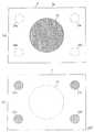
도 1 은 본 발명의 제조 방법의 실시형태의 요부를 나타내는 단면 공정도이다.
도 2 는 같은 실시형태에 있어서의 표시 장치의 제조 공정의 요부를 나타내는 평면도이다.
도 3 은 본 발명에 있어서의 수지 조성물 패턴의 예를 모식적으로 나타내는 도면이다.
도 4 는 본 발명에 있어서의 수지 조성물 패턴의 다른 예를 모식적으로 나타내는 도면이다
도 5 는 본 발명에 있어서의 수지 조성물 패턴의 다른 예를 모식적으로 나타내는 도면이다.
도 6 은 본 발명에 있어서의 수지 조성물 패턴의 다른 예를 모식적으로 나타내는 도면이다.
도 7 은 본 발명에 있어서의 수지 조성물 패턴의 다른 예를 모식적으로 나타내는 도면이다.
도 8 은 비교예의 수지 조성물 패턴의 예를 모식적으로 나타내는 도면이다.
도 9 는 종래 기술에 관련된 화상 표시 장치의 요부를 나타내는 단면도이다.1 is a cross-sectional process diagram showing a main part of an embodiment of a manufacturing method of the present invention.
2 is a plan view showing a main part of the manufacturing process of the display device in the embodiment.
3 is a diagram schematically showing an example of a resin composition pattern in the present invention.
4 is a diagram schematically showing another example of the resin composition pattern in the present invention
5 is a diagram schematically showing another example of the resin composition pattern in the present invention.
6 is a diagram schematically showing another example of the resin composition pattern in the present invention.
7 is a diagram schematically showing another example of the resin composition pattern in the present invention.
8 is a diagram schematically showing an example of a resin composition pattern of a comparative example.
9 is a cross-sectional view showing a main part of an image display apparatus related to the related art.
이하, 본 발명의 바람직한 실시형태를 도면을 참조하여 상세히 설명한다. 또한, 각 도면 중, 동일 부호는 동일 또는 동등한 구성 요소를 나타낸다.Hereinafter, preferred embodiments of the present invention will be described in detail with reference to the drawings. In the drawings, the same reference numerals denote the same or equivalent components.
도 1(a) ∼ 도 1(d) 는, 본 발명에 관련된 화상 표시 장치의 제조 방법의 하나의 실시형태의 요부를 나타내는 단면 공정도, 도 2 는, 같은 실시형태에 있어서의 화상 표시 장치의 제조 공정의 요부를 나타내는 평면도이다.1 (a) to 1 (d) are cross-sectional process drawings showing the essential part of one embodiment of a manufacturing method of an image display apparatus according to the present invention. Fig. 2 is a cross- 2 is a plan view showing a main part of the manufacturing process.
도 1(d) 에 나타내는 바와 같이, 본 실시형태에서는, 도시되지 않은 구동 회로에 접속되어 소정의 화상 표시를 실시하는 화상 표시부를 갖는 기부 (2) 와, 보호부 (3) 를 수지 경화물층 (14) 에 의해 부착시킨다.As shown in Fig. 1 (d), in this embodiment, a
여기에서, 화상 표시 장치 (1) 로는, 특별히 한정되지 않고, 여러 가지의 것에 적용할 수 있으며, 예를 들어, 휴대 전화, 휴대 게임 기기 등의 액정 표시 장치를 들 수 있다. 이하, 액정 표시 장치를 제조하는 경우를 예로 들어 본 발명을 설명한다.Here, the
보호부 (3) 는, 기부 (2) 와 동일한 정도의 크기의 판 형상, 시트 형상 또는 필름 형상의 투광성 부재 (4) 로 형성되어 있다. 이 투광성 부재 (4) 로는, 예를 들어, 광학 유리나 플라스틱 (폴리메틸메타크릴레이트 등의 아크릴 수지 등) 을 바람직하게 사용할 수 있다. 보호부 (3) 의 표면 혹은 이면에는, 반사 방지막, 차광막, 시야각 제어막 등의 광학층을 형성해도 된다.The
투광성 부재 (4) 의 기부 (2) 측의 면 (이하, 「도공면 (3a)」 이라고 한다) 의 주연 (周緣) 영역에 예를 들어 흑색 프레임 형상의 차광부 (5) 가 형성되어 있다. 이 차광부 (5) 는, 예를 들어 인쇄법에 의해 균일한 두께의 층 형상으로 형성되어 있다.A black frame-
보호부 (3) 의 도공면 (3a) 의 평탄함에 대해서는, 특별히 한정되지 않지만, 수지의 젖어 퍼짐 용이성이나 기포 혼입 방지의 관점에서는 가능한 한 평탄하게 하는 것이 바람직하다.The flatness of the coated
한편, 기부 (2) 는, 예를 들어 프레임 형상의 프레임 (6) 을 갖고, 이 프레임 (6) 의 내측 영역에 액정 표시 패널 (화상 표시부) (8) 이 장착되고, 또한 이 액정 표시 패널 (8) 의 장치 배면측 부위에 백라이트 (7) 가 장착되어 있다.On the other hand, the
또, 본 실시형태에서는, 기부 (2) 의 프레임 (6) 의 부착면 (6a) 과 보호부 (3) 의 차광부 (5) 의 부착면 (5a) 이 평행하게 되어 있다.In this embodiment, the
본 실시형태에서는, 이와 같은 보호부 (3) 와 기부 (2) 를 부착함에 있어서, 먼저, 도 1(a) 에 나타내는 바와 같이, 보호부 (3) 의 차광부 (5) 가 형성되어 있는 측의 표면에, 예를 들어 광경화형 수지 조성물을 소정량 적하하고, 각종 경화형 수지 조성물 (11) 의 패턴을 형성한다.In this embodiment, in attaching the
여기에서, 경화형 수지 조성물 (11) 의 적하량은, 보호부 (3) 와 기부 (2) 를 부착시킨 후의 수지 경화물층 (14) 의 두께를 50 ∼ 200 ㎛ 로 하는 것이 바람직하다.It is preferable that the thickness of the resin cured
또, 도 1 의 실시형태에서는, 보호부 (3) 에 경화형 수지 조성물 (11) 의 패턴을 형성하지만, 본 발명에 있어서, 경화형 수지 조성물 (11) 의 패턴은 기부 (2) 에 도공해도 되고, 보호부 (3) 및 기부 (2) 로 패턴을 나누어 도공해도 된다.1, the pattern of the
경화형 수지 조성물 (11) 의 패턴은, 기부 (2) 와 보호부 (3) 사이에 경화형 수지 조성물 (11) 을 균일한 두께로 골고루 미치게 함과 함께, 경화형 수지 조성물 (11) 로의 공기 혼입을 방지하는 면에서, 경화형 수지 조성물 (11) 을 도공한 후, 기부 (2) 와 보호부 (3) 를 근접 대향 배치한 경우에, 기부 (2) 와 보호부 (3) 의 대향면 전체에 경화형 수지 조성물이 퍼지도록 형성하는 것이 바람직하고, 보다 구체적으로는, 기부 (2) 또는 보호부 (3) 의 도공면의 중앙부에 위치하는 중앙부 패턴과, 그 중앙부 패턴보다 도공면의 귀퉁이부에 위치하며, 중앙부 패턴과 연속 또는 분리되어 있는 귀퉁이부 패턴으로 구성하는 것이 바람직하다. 이 패턴은 상호 간격을 두고 배치한 복수의 패턴이어도 된다.The pattern of the
도 3 ∼ 도 7 은, 직사각형 보호부 (3) 의 도공면 (3a) 에 경화형 수지 조성물 (11) 을 도공하는 경우의 수지 조성물 패턴의 구체예를 모식적으로 나타내는 것이다.Figs. 3 to 7 schematically show specific examples of the resin composition pattern when the
먼저, 도 3 에 나타내는 수지 조성물 패턴 (20) 은, 경화형 수지 조성물 (11) 을, 대략 알파벳 「Y」의 하측 부분을 이어 맞춘 연속 형상으로 형성한 것이다.First, the resin composition pattern 20 shown in Fig. 3 is obtained by forming the
이 수지 조성물 패턴 (20) 은, 보호부 (3) 의 장변 및 단변 방향 (XY 방향) 에 대해 대칭형이 되도록 형성되고, 수지 조성물 패턴 (20) 의 중심 (重心) 위치가 보호부 (3) 의 중심 위치 (점 G) 와 일치하도록 보호부 (3) 상에 배치되어 있다.This resin composition pattern 20 is formed to be symmetrical with respect to the long side and the short side direction (XY direction) of the
이 수지 조성물 패턴 (20) 은, 보호부 (3) 의 도공면 (3a) 의 중심부 영역의 중앙부 패턴 (21) 과, 중앙부 패턴 (21) 보다 도공면 (3a) 의 귀퉁이부에 위치하는 귀퉁이부 패턴으로 형성되어 있다.The resin composition pattern 20 has a
보다 구체적으로는, 중앙부 패턴 (21) 은, 상기 X 방향으로 직선 형상으로 연장된 띠형상의 패턴으로 형성되어 있다. 그리고, 귀퉁이부 패턴으로는, 중앙부 패턴 (21) 의 양 단부 (端部) 에서 4 방향으로 분기되어 연장된 아암부 패턴 (22a, 22b, 22c, 22d) 이 형성되어 있다.More specifically, the
이 아암부 패턴 (22a ∼ 22d) 은, 중앙부 패턴 (21) 의 양단부에서 보호부 (3) 의 각 귀퉁이부를 향하여 연장된 기준 직선 (4a ∼ 4d) 을 따라 직선 형상으로 형성되어 있고, 이로 인해, 각 아암부 패턴 (22a ∼ 22d) 의 선단부 (23a ∼ 23d) 가 보호부 (3) 의 각 귀퉁이부 근방에 위치하고 있다.The
여기에서, 수지 조성물 패턴 (20) 의 각 부분의 두께는, 반드시 균일할 필요는 없다. 본 발명에 있어서, 수지 조성물 패턴 (20) 의 바람직한 두께 분포는, 수지 조성물 패턴 (20) 의 형상도 따르지만, 기부 (2) 와 보호부 (3) 사이에 수지를 충전한 시점에서의 기포의 혼입을 확실히 방지하는 관점에서 보호부 (3) 의 도공면 (3a) 의 중심부 영역에서의 수지 조성물 패턴 (20) 의 두께를 주연부 영역에서의 수지 조성물 패턴의 두께보다 두껍게 하는 것이 바람직하다.Here, the thickness of each part of the resin composition pattern 20 is not necessarily uniform. In the present invention, the preferable thickness distribution of the resin composition pattern 20 depends on the shape of the resin composition pattern 20. However, when the resin is filled between the
도 4 에 나타내는 수지 조성물 패턴 (20B) 은, 보호부 (3) 의 도공면 (3a) 에 소정의 간격을 두고 배치한 복수의 패턴으로 구성되어 있다.The
즉, 도 4 의 수지 조성물 패턴 (20B) 도, 도 3 에 나타내는 수지 조성물 패턴 (20) 과 동일하게 Y 자를 이어 맞춘 형상을 갖고 있으나, 그 중앙부에서 보호부 (3) 의 각 귀퉁이부를 향하여 연장된 아암부 패턴 (22a ∼ 22d) 은, 도 3 의 아암부 패턴 (22a ∼ 22d) 에 비해 짧게 형성되어 있다.That is, the
그리고, 아암부 패턴의 선단부 (23a ∼ 23d) 와 보호부 (3) 의 도공면 (3a) 의 각 귀퉁이부 사이에, 각각 원형의 원형 수지 조성물 패턴 (24a, 24b, 24c, 24d) 이 형성되어 있다. 이들 각 원형 수지 조성물 패턴 (24a ∼ 24d) 은, 보호부 (3) 의 도공면 (3a) 의 각 귀퉁이부 영역의, 상기 서술한 각 기준 직선 (4a ∼ 4d) 상에 배치되어 있다.Circular
도 5 및 도 6 에 나타내는 예는, 도 4 에 나타낸 수지 조성물 패턴 (20B) 의 변형예를 나타내는 것이다.The examples shown in Figs. 5 and 6 show a modified example of the
도 5 에 나타내는 수지 조성물 패턴 (20C) 은, 보호부 (3) 의 도공면 (3a) 의 중심부 영역에 위치하는 중앙부 패턴 (21) 으로서, 보호부 (3) 와 거의 비슷한형상인 직사각형 패턴을 갖고 있고, 중앙부 패턴 (21) 의 네 귀퉁이와 보호부 (3) 의 도공면 (3a) 의 각 귀퉁이부 사이에, 귀퉁이부 패턴으로서, 중앙부 패턴 (21) 과 떨어진 원형 수지 조성물 패턴 (24a ∼ 24d) 을 갖고 있다.The
또, 도 6 에 나타내는 수지 조성물 패턴 (20D) 은, 보호부 (3) 의 도공면 (3a) 의 중심부 영역에 위치하는 중앙부 패턴 (21) 으로서, 원형 패턴을 갖고 있으며, 그 중심과 보호부 (3) 의 도공면 (3a) 의 각 귀퉁이부 사이에, 귀퉁이부 패턴으로서, 원형의 패턴으로부터 떨어진 원형 수지 조성물 패턴 (24a ∼ 24d) 을 갖고 있다.The
도 7 은, 수지 조성물 패턴을, 간격을 두고 배치한 복수의 패턴으로 구성하는 경우에, 보호부 (3) 와 기부 (2) 양방에 패턴을 배치한 예이다.7 shows an example in which a pattern is arranged on both the
즉, 도 7(a) 는, 도 6 의 수지 조성물 패턴 (20D) 중, 원형의 중앙부 패턴 (21) 을 보호부 (3) 의 중앙부 영역에 배치하고, 도 7(b) 는 같은 패턴 (20D) 의 원형 수지 조성물 패턴 (24a ∼ 24d) 을 기부 (2) 의 귀퉁이부 영역에 배치한 것이다.That is, in Fig. 7A, the circular
이 경우, 보호부 (3) 의 귀퉁이부 영역에 원형 수지 조성물 패턴 (24a ∼ 24d) 을 배치하고, 기부 (2) 의 중앙부 영역에 중앙부 패턴 (21) 을 형성할 수도 있지만, 기포 혼입 방지의 관점에서는, 도 7(a), 도 7(b) 에 나타내는 바와 같이, 보호부 (3) 에 중앙부 패턴 (21) 을 배치함과 함께, 기부 (2) 에 원형 수지 조성물 패턴 (24a ∼ 24d) 을 배치하는 것이 바람직하다.In this case, the circular
이상 설명한 모든 예에 있어서도, 경화형 수지 조성물 (11) 이 신속하게 균일한 두께로 보호부 (3) 와 기부 (2) 사이에 전체적으로 젖어 퍼지고, 또, 경화형 수지 조성물 (11) 로의 기포 혼입을 방지할 수 있다.In all the examples described above, too, the
특히, 경화형 수지 조성물 (11) 을 중앙부 패턴 (21) 으로 형성함으로써, 경화형 수지 조성물 (11) 이 기부 (2) 및 보호부 (3) 사이에서 젖어 퍼질 때에, 기부 (2) 및 보호부 (3) 의 가장자리부로부터 경화형 수지 조성물 (11) 이 비어져 나오기 어려워져, 귀퉁이부 패턴 (아암부 패턴 (22a ∼ 22d), 원형 수지 조성물 패턴 (24a ∼ 24d)) 으로 형성함으로써, 기부 (2) 및 보호부 (3) 의 가장자리부를 따라 경화형 수지 조성물 (11) 을 젖어 퍼지게 할 수 있게 된다.In particular, when the
또, 예를 들어, 도 4 ∼ 도 7 에 나타내는 바와 같이, 수지 조성물 패턴을, 소정의 간격을 두고 배치한 복수의 패턴으로 구성하는 경우에는, 기부 (2) 및 보호부 (3) 의 각 영역에서의 액정 표시 패널 (8) 등의 디바이스 상태나 전체적인 형상 등에 따라 경화형 수지 조성물 (11) 을 최적의 상태로 배치하고, 충전할 수 있게 된다.4 to 7, in the case where the resin composition pattern is formed of a plurality of patterns arranged at a predetermined interval, the resin composition pattern is formed in each region of the
게다가, 예를 들어, 도 7(a), 도 7(b) 에 나타내는 바와 같이, 수지 조성물 패턴 (20D) 중, 중앙부 패턴 (21) 을 보호부 (3) 에 배치하고, 귀퉁이부 패턴인 원형 수지 조성물 패턴 (24a ∼ 24d) 을 기부 (2) 에 배치함으로써, 이들 패턴을 서로 별도의 공정에서 형성할 수 있고, 이로써 더 나은 제조 공정의 신속화를 도모할 수 있게 된다.7A and 7B, among the
또한, 본 발명에 있어서, 수지 조성물 패턴의 형상이나 두께 등은, 상기 서술한 예에 한정되지 않고, 화상 표시 장치 (1) 의 패널의 형상 등에 따라 적절히 변경할 수 있다.In the present invention, the shape, the thickness, and the like of the resin composition pattern are not limited to the above-described examples, and can be appropriately changed according to the shape of the panel of the
또, 수지 조성물 패턴은, 인쇄법에 의해 형성할 수도 있다.The resin composition pattern may be formed by a printing method.
수지 조성물 패턴을 형성하는 경화형 수지 조성물 (11) 로는, 그 수지 경화물의 저장 탄성률 (25 ℃) 을 1 × 10⁷ Pa 이하, 바람직하게는 1 × 10³ ∼ 1 × 10⁶ Pa 로 하고, 수지 경화물의 굴절률을 바람직하게는 1.45 이상 1.55 이하, 보다 바람직하게는 1.51 이상 1.52 이하로 하고, 또한, 수지 경화물의 두께가 100 ㎛ 인 경우의 가시광 영역의 투과율을 90 % 이상으로 하도록 조제한 것을 사용한다.Roneun-
일반적으로, 경화형 수지 조성물을 구성하는 주요한 수지 성분으로는 공통되더라도, 함께 배합하는 수지 성분 혹은 모노머 성분 등이 상이하면, 그것을 경화시킨 수지 경화물의 저장 탄성률 (25 ℃) 이 1 × 10⁷ Pa 를 초과하는 경우가 있는데, 그와 같은 수지 경화물이 되는 수지 조성물은, 경화형 수지 조성물 (11) 로서는 사용하지 않는다.Generally, even if the main resin component constituting the curable resin composition is common, if the resin component or the monomer component to be mixed together is different, the cured resin hardened product has a storage elastic modulus (25 ° C) of more than 1 × 10⁷ Pa The resin composition which becomes such a resin cured product is not used as the curable resin composition (11).
또, 이 경화형 수지 조성물 (11) 은, 경화 수축률이 5.0 % 이하, 바람직하게는 4.5 % 이하, 보다 바람직하게는 4.0 % 이하, 더욱 바람직하게는 0 ∼ 2 % 가 되도록 조제한 것으로 한다. 이로 인해, 경화형 수지 조성물 (11) 이 경화될 때에 수지 경화물에 축적되는 내부 응력을 저감시킬 수 있어, 수지 경화물층 (14) 과 액정 표시 패널 (8) 또는 보호부 (3) 의 계면에서 변형이 생기는 것을 방지할 수 있다. 따라서, 경화형 수지 조성물 (11) 을 액정 표시 패널 (8) 과 보호부 (3) 사이에 개재시키고, 그 경화형 수지 조성물 (11) 을 경화시킨 경우에, 수지 경화물층 (14) 과 액정 표시 패널 (8) 또는 보호부 (3) 의 계면에서 발생하는 광의 산란을 저감시킬 수 있어, 표시 화상의 휘도를 높임과 함께, 시인성을 향상시킬 수 있다.The curable resin composition (11) is prepared so that the curing shrinkage percentage is 5.0% or less, preferably 4.5% or less, more preferably 4.0% or less, further preferably 0 to 2%. This makes it possible to reduce the internal stress accumulated in the resin cured product when the
또한, 수지 조성물이 경화될 때에 수지 경화물에 축적되는 내부 응력 정도는, 수지 조성물을 평판 상에 적하하고, 그것을 경화시켜 얻어지는 수지 경화물의 평균 표면 조도에 의해 평가할 수 있다. 예를 들어, 수지 조성물 2 ㎎ 을 유리판 상 또는 아크릴판 상에 적하하고, 그것을 UV 조사에 의해 90 % 이상의 경화율로 경화시켜 얻어지는 수지 경화물의 평균 표면 조도가 6.0 ㎚ 이하이면, 액정 표시 패널 (8) 과 보호부 (3) 사이에 경화형 수지 조성물을 개재시키고, 그것을 경화시킨 경우에 그들의 계면에서 발생되는 변형을 실용상 무시할 수 있다. 이에 관하여, 본 실시양태에서 사용하는 경화형 수지 조성물 (11) 에 의하면, 이 평균 표면 조도를 6.0 ㎚ 이하, 바람직하게는 5.0 ㎚ 이하, 보다 바람직하게는 1 ∼ 3 ㎚ 로 할 수 있다. 따라서, 수지 경화물의 계면에서 발생되는 변형을 실용상 무시할 수 있다.The degree of internal stress accumulated in the resin cured product when the resin composition is cured can be evaluated by the average surface roughness of the resin cured product obtained by dropping the resin composition on a flat plate and curing the resin composition. For example, when 2 mg of the resin composition is dropped onto a glass plate or an acrylic plate and the resulting cured product is cured at a curing rate of 90% or more by UV irradiation, the average surface roughness of the resin cured product is 6.0 nm or less, ) And the
여기에서, 유리판으로는, 액정셀의 액정을 협지하는 유리판이나 액정셀의 보호판으로서 사용되고 있는 것을 바람직하게 사용할 수 있다. 또한, 아크릴판으로는, 액정셀의 보호판으로서 사용되고 있는 것을 바람직하게 사용할 수 있다. 이들 유리판이나 아크릴판의 평균 표면 조도는, 통상 1.0 ㎚ 이하이다.Here, as the glass plate, those used as a glass plate for holding liquid crystal of the liquid crystal cell or a protective plate for a liquid crystal cell can be preferably used. As the acrylic plate, those used as a protective plate of a liquid crystal cell can be preferably used. The average surface roughness of these glass plates and acrylic plates is usually 1.0 nm or less.
또, 본 발명의 경우, 특별히 한정되지는 않지만, 젖어 퍼짐 속도나 비어져 나오기 어려움 관점에서는, 경화형 수지 조성물 (11) 로서는, 점도 (25 ℃, 콘플레이트형 회전 점도계, 콘플레이트의 테이퍼 각도 C35/2°, 10 rpm) 가 1000 mPa·s ∼ 5000 mPa·s 인 것을 사용하는 것이 바람직하고, 보다 바람직하게는 2000 mPa·s ∼ 3000 mPa·s 이다.In the case of the present invention, the viscosity (25 DEG C, cone plate type rotational viscometer, taper angle of cone plate C35 / cm) of the cone plate type rotational viscometer is used as the
구체적으로는, 예를 들어, 폴리우레탄아크릴레이트, 폴리이소프렌계 아크릴레이트 또는 그 에스테르화물, 테르펜계 수소 첨가 수지, 부타디엔 중합체 등의 1 종 이상의 폴리머와, 이소보르닐아크릴레이트, 디시클로펜테닐옥시에틸메타크릴레이트, 2-히드록시부틸메타크릴레이트 등의 1 종 이상의 아크릴레이트계 모노머와, 1-히드록시-시클로헥실-페닐-케톤 등의 광중합 개시제를 함유하는 수지 조성물을 바람직하게 사용할 수 있다. 그 밖의 첨가제, 예를 들어 증감제, 가소제, 투명 입자 등을 본 발명의 목적 범위에서 첨가할 수도 있다.Specifically, for example, at least one polymer such as polyurethane acrylate, polyisoprene acrylate or esterified product thereof, terpene hydrogenated resin, butadiene polymer and the like, and at least one polymer selected from the group consisting of isobornyl acrylate, dicyclopentenyloxy A resin composition containing at least one acrylate monomer such as ethyl methacrylate and 2-hydroxybutyl methacrylate and a photopolymerization initiator such as 1-hydroxy-cyclohexyl-phenyl-ketone can be preferably used . Other additives such as sensitizers, plasticizers, transparent particles and the like may be added within the object of the present invention.
여기에서, 광중합 개시제로는, 1-히드록시-시클로헥실-페닐-케톤 (상품명 IRGACURE (이르가큐어) 184 : 치바·스페셜리티·케미컬즈(주) 제조) 등을 바람직하게 사용할 수 있다.As the photopolymerization initiator, 1-hydroxy-cyclohexyl-phenyl-ketone (trade name IRGACURE (Irgacure) 184: manufactured by Chiba Specialty Chemicals Co., Ltd.) can be preferably used.
또, 보호부 (3) 는, 표시부에 대한 자외선 보호의 관점에서 자외선 영역을 컷하는 기능이 부여되어 있는 경우가 있다. 그 경우에는, 광중합 개시제로서는, 가시광 영역에서도 경화시킬 수 있는 광중합 개시제 (예를 들어, 상품명 SpeedCureTPO : 니혼 시베르헤그너(주) 제조 등) 를 사용하는 것이 바람직하다.In addition, the
도 1 의 실시형태에 있어서, 보호부에 경화형 수지 조성물 (11) 의 패턴을 도공한 후에는, 도 1(b) 에 나타내는 바와 같이, 보호부 (3) 의 표리를 뒤집어 경화형 수지 조성물 (11) 의 패턴을 형성한 면을 연직 하방으로 향하여 보호부 (3) 를 기부 (2) 의 상방에 대향 배치시킨다. 이로 인해, 도공한 경화형 수지 조성물 (11) 의 표면이, 보호부 (3) 의 도공면 (3a) 의 표면 형상의 영향을 받기 어려워지고, 게다가 중력과 경화형 수지 조성물 (11) 의 표면 장력의 합력에 의해 수지 조성물 패턴 (11) 의 표면이 보다 매끄러워지기 때문에, 기부 (2) 와 보호부 (3) 사이에 충전되는 수지의 두께를 더욱 균일하게 할 수 있음과 함께, 경화형 수지 조성물 (11) 로의 기포 혼입을 확실히 방지할 수 있다.1 (b), after the pattern of the
이어서, 위치 결정 승강 기구와 위치 결정 수단 (도시 생략) 에 의해, 보호부 (3) 를 수평으로 유지한 상태에서 하강시키고, 기부 (2) 와 보호부 (3) 사이의 간격을 정하기 위한 스페이서를 사용하지 않고, 보호부 (3) 를 소정의 위치에 고정시키고, 보호부 (3) 에 도공한 경화형 수지 조성물 (11) 을 기부 (2) 의 표면에 접촉시켜, 기부 (2) 와 보호부 (3) 사이의 공극에 경화형 수지 조성물 (11) 을 충전한다.Next, a spacer for lowering the protecting
그 후, 도 1(c) 에 나타내는 바와 같이, 화상 표시 영역에 대응하는 수지 조성물 충전부 (13) 에 대해, 투광성 부재 (4) 를 통해 자외선 (33) 을 조사한다.1 (c), ultraviolet rays 33 are irradiated to the resin-filled
자외선 (33) 의 조사 방향은, 특별히 한정되지 않지만, 화상 표시 영역에 있는 경화형 수지 조성물 (11) 의 보다 균일한 경화를 더욱 달성하는 관점에서는, 투광성 부재 (4) 의 표면에 대해 직교하는 방향으로 하는 것이 바람직하다.The direction of irradiation of the
또, 이와 동시에, 도 1(c) 및 도 2 에 나타내는 바와 같이, 예를 들어 광파이버 등으로 이루어지는 미세한 조사부 (30) 를 갖는 UV 광 조사 장치 (31) 를 사용하여, 차광부 (5) 와 기부 (2) 사이의 수지 조성물 충전부 (12) 에 대해, 차광부 (5) 의 부착면 (5a) 의 외방 측면측에서 자외선 (32) 을 직접 조사해도 된다.At the same time, as shown in Fig. 1 (c) and Fig. 2, by using the UV
자외선 (32) 의 조사 방향은, 특별히 한정되지 않지만, 수평 방향에 대해 0° 이상 90° 미만으로 할 수 있는데, 차광부 (5) 의 형성 영역에 있는 경화형 수지 조성물 (11) 의 보다 균일한 경화를 달성하는 관점에서는, 기부 (2) 의 프레임 (6) 의 부착면 (6a) 과 보호부 (3) 의 차광부 (5) 의 부착면 (5a) 에 대해, 거의 평행하게 자외선 (32) 의 조사를 실시하는 것이 바람직하다.Although the irradiation direction of the
이와 같은 자외선 (32, 33) 의 조사를 실시함으로써, 도 1(d) 에 나타내는 바와 같이, 수지 조성물 충전부 (12, 13) 를 경화시켜 수지 경화물층 (14) 으로 하고, 목적으로 하는 화상 표시 장치 (1) 를 얻는다.By irradiating such
또한, 본 발명은 상기 실시형태에 한정되지 않으며, 여러 가지의 변경을 실시할 수 있다.The present invention is not limited to the above embodiment, and various modifications can be made.
예를 들어, 화상 표시 영역에 대응하는 경화형 수지 조성물 (11) 에 대한 자외선 (33) 의 조사와, 차광부에 대응하는 경화형 수지 조성물 (11) 에 대한 자외선 (32) 의 조사는, 동시에 실시해도 되고, 또 별도의 공정으로 실시해도 된다.For example, the irradiation of the
또한, 본 발명은 상기 서술한 액정 표시 장치뿐만 아니라, 예를 들어, 유기 EL, 플라즈마 디스플레이 장치 등의 각종 패널 디스플레이에 적용할 수 있다.The present invention can be applied not only to the above-described liquid crystal display device but also to various panel displays such as organic EL, plasma display devices and the like.
실시예Example
이하, 실시예 및 비교예를 들어 본 발명을 구체적으로 설명하는데, 본 발명은 이하의 실시예에 한정되지 않는다.Hereinafter, the present invention will be specifically described with reference to Examples and Comparative Examples, but the present invention is not limited to the following Examples.
〔도공액의 조제〕[Preparation of Coating Solution]
<실시예 수지 1>≪
폴리우레탄아크릴레이트 (상품명 UV-3000B, 닛폰 합성화학공업(주) 제조) 50 중량부, 이소보르닐아크릴레이트 (상품명 IBXA, 오사카 유기화학공업(주) 제조) 30 중량부, 광중합 개시제 (상품명 이르가큐어 184, 치바·스페셜리티·케미컬즈(주) 제조) 3 중량부, 광중합 개시제 (상품명 SpeedCureTPO, 니혼 시베르헤그너(주) 제조) 1 중량부를 혼련기로 혼련하여 실시예 1 의 수지 조성물을 조제하였다.50 parts by weight of polyurethane acrylate (trade name UV-3000B, manufactured by Nippon Synthetic Chemical Industry Co., Ltd.), 30 parts by weight of isobornyl acrylate (trade name IBXA, Osaka Organic Chemical Industry Co., Ltd.) (Trade name: SpeedCure TPO, manufactured by Nippon Shokubera Co., Ltd.) were kneaded with a kneader to prepare a resin composition of Example 1 (manufactured by Nippon Shokubai Kogyo Co., Ltd.) Respectively.
<실시예 수지 2>≪
폴리이소프렌 중합물의 무수 말레산 부가물과 2-히드록시에틸메타크릴레이트의 에스테르화물 70 중량부, 디시클로펜테닐옥시에틸메타크릴레이트 30 중량부, 2-히드록시부틸메타크릴레이트 10 중량부, 테르펜계 수소 첨가 수지 30 중량부, 부타디엔 중합체 140 중량부, 광중합 개시제 4 중량부, 가시광 영역용 광중합 개시제 0.5 중량부를 혼련기로 혼련하여 실시예 2 의 수지 조성물을 조제하였다.70 parts by weight of the maleic anhydride adduct of the polyisoprene polymer and 2-hydroxyethyl methacrylate, 30 parts by weight of dicyclopentenyloxyethyl methacrylate, 10 parts by weight of 2-hydroxybutyl methacrylate, , 30 parts by weight of a terpene type hydrogenated resin, 140 parts by weight of a butadiene polymer, 4 parts by weight of a photopolymerization initiator, and 0.5 parts by weight of a photopolymerization initiator for a visible light region were kneaded with a kneader to prepare a resin composition of Example 2.
<실시예 수지 3>≪ Example 3 >
폴리이소프렌 중합물의 무수 말레산 부가물과 2-히드록시에틸메타크릴레이트의 에스테르화물 100 중량부, 디시클로펜테닐옥시에틸메타크릴레이트 30 중량부, 2-히드록시부틸메타크릴레이트 10 중량부, 테르펜계 수소 첨가 수지 30 중량부, 부타디엔 중합체 210 중량부, 광중합 개시제 7 중량부, 가시광 영역용 광중합 개시제 1.5 중량부를 혼련기로 혼련하여 실시예 3 의 수지 조성물을 조제하였다.100 parts by weight of the maleic anhydride adduct of the polyisoprene polymer and 2-hydroxyethyl methacrylate, 30 parts by weight of dicyclopentenyloxyethyl methacrylate, 10 parts by weight of 2-hydroxybutyl methacrylate, 30 parts by weight of a terpene type hydrogenated resin, 210 parts by weight of a butadiene polymer, 7 parts by weight of a photopolymerization initiator, and 1.5 parts by weight of a photopolymerization initiator for visible light region were kneaded by a kneader to prepare a resin composition of Example 3.
<실시예 수지 4><
폴리이소프렌 중합물의 무수 말레산 부가물과 2-히드록시에틸메타크릴레이트의 에스테르화물 (상품명 UC-203, (주)쿠라레 제조) 70 중량부, 디시클로펜테닐옥시에틸메타크릴레이트 (상품명 FA512M, 히타치 화성공업(주) 제조) 30 중량부, 2-히드록시부틸메타크릴레이트 (상품명 라이트에스테르 HOB, 쿄에이샤 화학(주) 제조) 10 중량부, 테르펜계 수소 첨가 수지 (상품명 크리아론 P-85, 야스하라 케미컬(주) 제조) 30 중량부, 부타디엔 중합체 (상품명 Polyoil110, 닛폰 제온(주) 제조) 35 중량부, 광중합 개시제 (상품명 이르가큐어 184D, 치바·스페셜리티·케미컬즈(주) 제조) 5 중량부, 광중합 개시제 (상품명 SpeedCureTPO, 니혼 시베르헤그너(주) 제조) 2 중량부를 혼련기로 혼련하여 실시예 4 의 수지 조성물을 조제하였다.70 parts by weight of an anhydrous maleic acid adduct of polyisoprene polymer and 2-hydroxyethyl methacrylate esterified product (trade name UC-203, manufactured by Kuraray Co., Ltd.), dicyclopentenyloxyethyl methacrylate (trade name: FA512M , 10 parts by weight of 2-hydroxybutyl methacrylate (trade name: Light Ester HOB, manufactured by Kyowa Chemical Industry Co., Ltd.), 30 parts by weight of a terpene hydrogenated resin (trade name: Cryaron P 35 parts by weight of a butadiene polymer (trade name: Polyoil 110, manufactured by Nippon Zeon Co., Ltd.), 30 parts by weight of a photopolymerization initiator (trade name IRGACURE 184D, manufactured by Chiba Specialty Chemicals Co., Ltd.) and 2 parts by weight of a photopolymerization initiator (trade name: SpeedCure TPO, manufactured by Nihon Shimadzu) were kneaded with a kneader to prepare a resin composition of Example 4.
<비교예 수지 1>≪
폴리부타디엔아크릴레이트 (상품명 TE-2000, 닛폰 소다(주) 제조) 50 중량부, 히드록시에틸메타크릴레이트 (상품명 라이트에스테르 HO, 쿄에이샤 화학(주) 제조) 20 중량부, 광중합 개시제 (상품명 이르가큐어 184, 치바·스페셜리티·케미컬즈(주) 제조) 3 중량부, 광중합 개시제 (상품명 SpeedCureTPO, 니혼 시베르헤그너(주) 제조) 1 중량부를 혼련기로 혼련하여 비교예 1 의 수지 조성물을 조제하였다.50 parts by weight of polybutadiene acrylate (trade name: TE-2000, manufactured by Nippon Soda Co., Ltd.), 20 parts by weight of hydroxyethyl methacrylate (trade name: Light Ester HO, Kyowa Chemical Co., (Trade name: SpeedCure TPO, manufactured by Nippon Shokubera Co., Ltd.) were kneaded with a kneader to obtain a resin composition of Comparative Example 1, Lt; / RTI >
<비교예 수지 2> ≪
폴리우레탄아크릴레이트 (상품명 UV-3000B, 닛폰 합성화학공업(주) 제조) 50 중량부, 트리시클로데칸디메탄올아크릴레이트 (상품명 NK 에스테르 LC2, 신나카무라 화학공업(주) 제조) 30 중량부, 광중합 개시제 (이르가큐어 184, 치바·스페셜리티·케미컬즈(주) 제조) 3 중량부, 광중합 개시제 (상품명 SpeedCureTPO, 니혼 시베르헤그너(주) 제조) 1 중량부를 혼련기로 혼련하여 비교예 2 의 수지 조성물을 조제하였다.50 parts by weight of polyurethane acrylate (trade name UV-3000B, manufactured by Nippon Synthetic Chemical Industry Co., Ltd.), 30 parts by weight of tricyclodecane dimethanol acrylate (trade name: NK Ester LC2, Shin Nakamura Chemical Industry Co., Ltd.) , 3 parts by weight of an initiator (Irgacure 184, manufactured by Chiba Specialty Chemicals Co., Ltd.) and 1 part by weight of a photopolymerization initiator (trade name: SpeedCure TPO, manufactured by Nippon Shokubera Co., Ltd.) A composition was prepared.
<비교예 수지 3>≪
폴리부타디엔아크릴레이트 (상품명 TE-2000, 닛폰 소다(주) 제조) 50 중량부, 이소보르닐아크릴레이트 (상품명 IBXA, 오사카 유기화학공업(주) 제조) 20 중량부, 광중합 개시제 (상품명 이르가큐어 184, 치바·스페셜리티·케미컬즈(주) 제조) 3 중량부, 광중합 개시제 (상품명 SpeedCureTPO, 니혼 시베르헤그너(주) 제조) 1 중량부를 혼련기로 혼련하여 비교예 3 의 수지 조성물을 조제하였다.50 parts by weight of polybutadiene acrylate (trade name: TE-2000, manufactured by Nippon Soda Co., Ltd.), 20 parts by weight of isobornyl acrylate (trade name: IBXA, Osaka Organic Chemical Industry Co., Ltd.) 184, manufactured by Chiba Specialty Chemicals Co., Ltd.), and 1 part by weight of a photopolymerization initiator (trade name: SpeedCure TPO, manufactured by Nippon Shokuber Hegner Co., Ltd.) were kneaded with a kneader to prepare a resin composition of Comparative Example 3.
평가 1
실시예 수지 1 ∼ 4, 비교예 수지 1 ∼ 3 에서 조제한 수지 조성물에 대하여, 다음과 같이 광투과율, 저장 탄성률, 경화 수축률, 표면 조도를 측정하였다. 이들의 결과를 표 1 에 나타낸다.The light transmittance, storage modulus, curing shrinkage and surface roughness of the resin compositions prepared in
〔광투과율〕[Light transmittance]
각 수지 조성물을, 두께 100 ㎛ 의 백색 유리판 상에 소정의 막 두께가 되도록 적하하고, 자외선 조사 장치 내의 UV 컨베이어로 반송하여 수지를 경화시킨 것을 시료로 하였다.Each of the resin compositions was dropped onto a white glass plate having a thickness of 100 占 퐉 so as to have a predetermined film thickness and transported to a UV conveyer in an ultraviolet irradiator to cure the resin.
각 시료 (수지 경화물의 두께 100 ㎛) 에 대하여, 자외 가시 분광 광도계 (닛폰 분광(주) 제조 V-560) 에 의해 가시광 영역의 투과율 (%) 을 측정하였다.The transmittance (%) in the visible light region was measured by an ultraviolet visible spectrophotometer (V-560, manufactured by Nippon Bunko K.K.) for each sample (thickness of the resin cured product: 100 mu m).
〔저장 탄성률〕[Storage elastic modulus]
광투과율의 시료와 동일하게 제조한 각 시료에 대하여, 점탄성 측정 장치 (세이코인스트루먼트(주) 제조 DMS6100) 를 사용하여 저장 탄성률 (Pa) (측정 주파수 1 Hz, 25 ℃) 을 측정하였다.The storage elastic modulus (Pa) (
〔경화 수축률〕[Curing shrinkage rate]
경화 수축률 (%) 에 대해서는, 경화 전의 수지액과 경화 후의 고체 비중을 전자 비중계 (MIRAGE 사 제조 SD-120L) 를 사용하여 측정하고, 양자의 비중차에 기초하여 다음 식으로부터 산출하였다.The hardening shrinkage percentage (%) was calculated from the following formula based on the difference in specific gravity between the resin before curing and the solid specific gravity after curing using an electronic gravity meter (SD-120L manufactured by MIRAGE).
[수학식 1][Equation 1]
경화 수축률 (%) = (경화물 비중 - 수지액 비중)/경화물 비중 × 100Cure shrinkage (%) = (Specific gravity of cured product - Specific gravity of resin solution) / Specific gravity of cured product × 100
〔표면 조도의 측정〕[Measurement of surface roughness]
각 수지 조성물에 대하여, 각각 2 ㎎ 을 액정셀용 유리판에 적하하고, 자외선 조사에 의한 경화 반응시에 생기는 내부 응력에 의해 발생하는 유리판 표면의 소정 영역 (2.93 ㎜ × 2.20 ㎜) 의 변형 (Ra : 평균 표면 조도) 을, Zygo 사 제조 3 차원 비접촉 표면 조도 측정계로 측정하였다.2 mg of each resin composition was dropped on a glass plate for a liquid crystal cell, and the deformation (Ra: average value) of a predetermined area (2.93 mm x 2.20 mm) of the surface of the glass plate caused by internal stress generated during the curing reaction by ultraviolet irradiation Surface roughness) was measured with a three-dimensional non-contact surface roughness meter manufactured by Zygo Corporation.
표 1 에서 알 수 있는 바와 같이, 투과율에 대해서는 실시예 수지 및 비교예 수지 모두 문제없이 양호한 결과를 얻을 수 있었다.As can be seen from Table 1, with respect to the transmittance, both the resin of Example and the resin of Comparative Example were able to obtain satisfactory results without any problem.
한편, 실시예 수지 1 ∼ 4 는, 저장 탄성률이 4 × 10³ ∼ 1 × 10⁶ Pa 이고, 또한, 경화 수축률에 대해서는 1.0 ∼ 4.5 % 이며, 그 때문에, 평균 표면 조도 Ra = 1.5 ∼ 5.5 ㎚ 로 변형이 거의 없어, 양호한 결과를 얻을 수 있었다.On the other hand, the
이에 대해, 비교예 수지 1 (Ra = 12.4 ㎚), 비교예 수지 2 (Ra = 36.5 ㎚), 비교예 수지 3 (Ra = 64.2 ㎚) 은, 평균 표면 조도 Ra 가 커, 수지가 경화될 때의 내부 응력에 의해 수지와 유리판의 계면이 변형되는 것이 이해된다.In contrast, Comparative Example Resin 1 (Ra = 12.4 nm), Comparative Resin 2 (Ra = 36.5 nm) and Comparative Example Resin 3 (Ra = 64.2 nm) had a large average surface roughness Ra, It is understood that the interface between the resin and the glass plate is deformed by the internal stress.
평가 2
실시예 수지 1 ∼ 4 의 수지 조성물을 사용하여, 도 1 의 실시예 패턴 및 도 8 의 비교예 패턴에 대하여, 수지 조성물이 젖어 퍼지는 시간과 두께의 편차를 다음과 같이 평가하였다. 결과를 표 2 에 나타낸다.EXAMPLES Using the resin compositions of
<실시예 패턴><Example Pattern>
실시예 수지 1 의 수지 조성물을 사용하여, 도 1 의 화상 표시 장치의 보호부 (3) 측의 도공면 (3a) 에, 상기 서술한 도 4 에 나타내는 수지 조성물 패턴 (21) 및 원형 수지 조성물 패턴 (24a ∼ 24d) 을 형성하고, 뒤집은 상태에서 기부 (2) 측의 액정 표시 패널 (8) 에 대해 평행하게 근접 대향 배치하고, 기부 (2) 및 보호부 (3) 사이에 수지 조성물을 젖어 퍼지게 하였다.Example 1 Using the resin composition of the
실시예 수지 2 ∼ 4 의 수지 조성물을 사용하여, 실시예 수지 1 의 수지 조성물과 동일하게 기부 (2) 및 보호부 (3) 사이에 수지 조성물을 젖어 퍼지게 하였다.Using the resin compositions of Examples 2 to 4, the resin composition was wetted between the
<비교예 패턴><Comparative Example Pattern>
실시예 수지 1 의 수지 조성물을 사용하여, 보호부 (3) 의 도공면 (3a) 의 중앙 부분에 도 8 에 나타내는 타원형 패턴 (50) 을 형성하는 것 이외에는, 상기 서술과 동일하게 기부 (2) 및 보호부 (3) 사이에 수지 조성물을 젖어 퍼지게 하였다.Except that the
〔수지 두께의 편차 측정〕[Measurement of Deviation of Resin Thickness]
기부 (2) 및 보호부 (3) 사이에 충전한 수지 조성물에 대하여, 젖어 퍼짐 시간 및 수지 두께의 편차를 산출하였다.The deviation of the wetting spread time and the resin thickness was calculated for the resin composition filled between the
수지 두께의 편차는, 기부 (2) 와 보호부 (3) 가 부착된 화상 표시 장치 (도 1(d)) 의 전체 두께를, 부착 영역의 중앙부와 네 귀퉁이의 합계 5 지점에 대하여 막후계 (μ메이트, 소니사 제조) 로 측정하고, 각 측정값의 기준 두께 (100 ㎛) 에 대한 편차의 비율 (%) 을 구하고, 그 분산 (σ2) 으로부터 구하였다.The deviation of the thickness of the resin can be measured by measuring the total thickness of the image display device (Fig. 1 (d)) to which the
(실시예 수지 1 ∼ 4)Example Pattern
(Examples Resins 1 to 4)
0.1
0.1
5 % 이하
Less than 5%
(실시예 수지 1)Comparative Example Pattern
(Example resin 1)
1
One
30 %
30%
표 2 에서 알 수 있는 바와 같이, 수지 조성물의 젖어 퍼짐 시간에 대해서는, 실시예 수지 1 ∼ 4 모두에 대해서, 실시예 패턴의 경우에는, 비교예 패턴의 경우에 비해 1/10 의 젖어 퍼짐 시간에 수지 조성물을 충전할 수 있었다.As can be seen from Table 2, the wetting spread time of the resin composition was about 1/10 of the spreading time of the wetting spreading agent in all of Examples 1 to 4, in the case of the example pattern, The resin composition could be filled.
한편, 수지 두께의 편차에 대해서는, 비교예 패턴의 경우 (30 %) 에 비해, 실시예 패턴은 양호한 결과가 얻어졌다.On the other hand, with respect to the deviation of the thickness of the resin, a good result of the example pattern was obtained as compared with the case of the comparative example pattern (30%).
이 경우, 실시예 수지 1 에 있어서는 수지 두께의 편차가 5 % 이고, 실시예 수지 2 ∼ 4 에 있어서는 5 % 미만이었다.In this case, the variation in the thickness of the resin in Example 1 was 5%, and that in Example 2 to 4 was less than 5%.
이들 결과에서 본 발명에 의하면, 화상 표시 장치의 기부 (2) 와 보호부 (3) 사이에 수지 조성물을 균일한 두께로 단시간에 충전할 수 있는 것으로 이해된다.From these results, it can be understood that the present invention can fill the resin composition between the
산업상 이용가능성Industrial availability
본 발명은 액정 표시 장치 등의 화상 표시 장치의 제조에 유용하다.The present invention is useful for manufacturing an image display device such as a liquid crystal display device.
1 : 화상 표시 장치
2 : 기부
3 : 보호부
3a : 도공면
4 : 투광성 부재
5 : 차광부
5a : 차광부의 부착면
6 : 프레임
6a : 프레임의 부착면
8 : 액정 표시 패널 (화상 표시부)
11 : 경화형 수지 조성물
12 : 차광부와 기부 사이의 수지 조성물 충전부
13 : 화상 표시 영역에 대응하는 수지 조성물 충전부
14 : 수지 경화물층
20, 20B, 20C, 20D : 수지 조성물 패턴
21 : 중앙부 패턴
22a, 22b, 22c, 22d : 아암부 패턴
23a, 23b, 23c, 23d : 아암부 패턴의 선단부
24a, 24b, 24c, 24d : 원형 수지 조성물 패턴
32, 33 : 자외선1: Image display device
2: donation
3: Protection section
3a: Coated surface
4: Light-transmissive member
5:
5a: Mounting surface of light shield
6: frame
6a: Mounting surface of the frame
8: Liquid crystal display panel (image display section)
11: Curing type resin composition
12: a resin composition charging part between the light-shielding part and the base
13: a resin composition charging section corresponding to the image display region
14: Cured resin layer
20, 20B, 20C, 20D: Resin composition pattern
21: Center pattern
22a, 22b, 22c, 22d:
23a, 23b, 23c, and 23d:
24a, 24b, 24c, and 24d: a circular resin composition pattern
32, 33: ultraviolet ray
Claims (12)
Translated fromKorean경화형 수지 조성물로서, 가소제 (단, 테르펜계 수소 첨가 수지와 부타디엔 중합체를 제외한다) 와, 아크릴레이트계 모노머와 광중합 개시제를 함유하고, 그 경화형 수지 조성물의 상기 아크릴레이트계 모노머가 상기 광중합 개시제의 작용에 기초하여 생긴 경화율이 90 % 이상에 도달하는 과정에서 생기는 경화 수축률이 4.0 % 이하 또한 경화물의 25 ℃ 에 있어서의 저장 탄성률이 1 × 10⁷ Pa 이하로 조정되고, 수지 경화물층의 가시광 영역의 광투과율을 90 % 이상으로 하는 수지 조성물을 사용하고,
화상 표시부 또는 보호부에 도공하는 경화형 수지 조성물을 특정 형상의 패턴으로 하고, 화상 표시부와 보호부를 근접 대향 배치함으로써 경화형 수지 조성물을 화상 표시부 및 보호부 사이에 퍼지게 하고, 이어서 경화형 수지 조성물을 경화시키는, 화상 표시 장치의 제조 방법.A curable resin composition is applied to an image display unit or a translucent protective unit disposed on the image display unit and the image display unit and the protective unit are arranged close to each other and cured to form a resin cured layer between the image display unit and the protective unit A method of manufacturing an image display apparatus having a step of forming a light-
A curable resin composition comprising a plasticizer (excluding terpene-based hydrogenation resin and butadiene polymer), an acrylate-based monomer and a photopolymerization initiator, wherein the acrylate-based monomer of the curable resin composition has a function of the photopolymerization initiator , The storage modulus of the cured product at 25 DEG C is adjusted to 1 x 10 <7 > Pa or less, and the cured product of the cured product in the visible light region Is 90% or more, and the light transmittance of the resin composition
The curable resin composition coated on the image display portion or the protective portion has a specific pattern and the curable resin composition is spread between the image display portion and the protective portion by disposing the image display portion and the protective portion in close proximity to each other to cure the curable resin composition, A method of manufacturing an image display device.
경화형 수지 조성물을 도공한 후, 화상 표시부와 보호부를 근접 대향 배치한 경우에, 화상 표시부와 보호부의 대향면 전체에 경화형 수지 조성물이 퍼지도록 경화형 수지 조성물의 패턴을 형성하는, 화상 표시 장치의 제조 방법.The method according to claim 1,
A method of manufacturing an image display device, which forms a pattern of a curable resin composition so that the curable resin composition spreads over the entire opposing surfaces of the image display portion and the protective portion when the image display portion and the protective portion are arranged close to each other after coating the curable resin composition .
경화형 수지 조성물의 패턴을, 화상 표시부 또는 보호부의 도공면의 중앙부에 위치하는 중앙부 패턴과, 그 중앙부 패턴보다 도공면의 귀퉁이부에 위치하며, 중앙부 패턴과 연속 또는 분리되어 있는 귀퉁이부 패턴으로 구성하는, 화상 표시 장치의 제조 방법.3. The method of claim 2,
The pattern of the curable resin composition is composed of a central pattern positioned at the center of the coated surface of the image display portion or the protective portion and a corner pattern located at the corner of the coated surface, , And a manufacturing method of an image display apparatus.
경화형 수지 조성물의 패턴을, 간격을 두고 배치한 복수의 패턴으로 구성하는, 화상 표시 장치의 제조 방법.The method according to claim 1,
Wherein the pattern of the curable resin composition is constituted by a plurality of patterns arranged at intervals.
경화형 수지 조성물을 화상 표시부 또는 보호부에 도공한 후, 그 도공면을 연직 하방으로 향한 상태에서 화상 표시부와 보호부를 근접 대향 배치하는, 화상 표시 장치의 제조 방법.The method according to claim 1,
Wherein the curable resin composition is coated on an image display portion or a protective portion, and then the image display portion and the protective portion are arranged close to each other in a state in which the coated surface faces downward.
경화형 수지 조성물을 화상 표시부와 보호부 양방에 도공하는, 화상 표시 장치의 제조 방법.The method according to claim 1,
Wherein the curable resin composition is coated on both the image display portion and the protective portion.
수지 경화물층의 25 ℃ 에 있어서의 저장 탄성률이 1 × 10³ ∼ 1 × 10⁶ Pa 인, 화상 표시 장치의 제조 방법.The method according to claim 1,
Of the storage elastic modulus at 25 ℃ of the resin cured layer1 × 10 3 ~ 1 × 10 6 Pa, manufacturing method of an image displaying apparatus.
수지 경화물층의 두께가 50 ∼ 200 ㎛ 인, 화상 표시 장치의 제조 방법.The method according to claim 1,
Wherein the thickness of the resin cured layer is 50 to 200 占 퐉.
표시부가 액정 표시 패널인, 화상 표시 장치의 제조 방법.The method according to claim 1,
And the display portion is a liquid crystal display panel.
보호부가 아크릴 수지로 이루어지는, 화상 표시 장치의 제조 방법.The method according to claim 1,
Wherein the protective portion is made of an acrylic resin.
보호부가 광학 유리로 이루어지는, 화상 표시 장치의 제조 방법.The method according to claim 1,
Wherein the protective portion is made of optical glass.
Applications Claiming Priority (9)
| Application Number | Priority Date | Filing Date | Title |
|---|---|---|---|
| JPJP-P-2007-102938 | 2007-04-10 | ||
| JP2007102938 | 2007-04-10 | ||
| JPJP-P-2007-186360 | 2007-07-17 | ||
| JP2007186360 | 2007-07-17 | ||
| JP2008005027 | 2008-01-11 | ||
| JPJP-P-2008-005027 | 2008-01-11 | ||
| JP2008005096 | 2008-01-13 | ||
| JPJP-P-2008-005096 | 2008-01-13 | ||
| PCT/JP2008/057070WO2008126893A1 (en) | 2007-04-10 | 2008-04-10 | Method for manufacturing image display device, and image display device |
Related Parent Applications (1)
| Application Number | Title | Priority Date | Filing Date |
|---|---|---|---|
| KR1020177001069ADivisionKR101749478B1 (en) | 2007-04-10 | 2008-04-10 | Method for manufacturing image display device, and image display device |
Related Child Applications (1)
| Application Number | Title | Priority Date | Filing Date |
|---|---|---|---|
| KR1020187018731ADivisionKR102185076B1 (en) | 2007-04-10 | 2008-04-10 | Method for manufacturing image display device, and image display device |
Publications (1)
| Publication Number | Publication Date |
|---|---|
| KR20170072360Atrue KR20170072360A (en) | 2017-06-26 |
Family
ID=39863988
Family Applications (11)
| Application Number | Title | Priority Date | Filing Date |
|---|---|---|---|
| KR1020177016187ACeasedKR20170072360A (en) | 2007-04-10 | 2008-04-10 | Method for manufacturing image display device, and image display device |
| KR1020177001069AActiveKR101749478B1 (en) | 2007-04-10 | 2008-04-10 | Method for manufacturing image display device, and image display device |
| KR1020207033926AActiveKR102391043B1 (en) | 2007-04-10 | 2008-04-10 | Method for manufacturing image display device, and image display device |
| KR1020227013745AAbandonedKR20220058652A (en) | 2007-04-10 | 2008-04-10 | Method for manufacturing image display device, and image display device |
| KR1020247013317APendingKR20240060694A (en) | 2007-04-10 | 2008-04-10 | Method for manufacturing image display device, and image display device |
| KR1020157008267AActiveKR101636824B1 (en) | 2007-04-10 | 2008-04-10 | Method for manufacturing image display device, and image display device |
| KR1020097021192ACeasedKR20090129466A (en) | 2007-04-10 | 2008-04-10 | The manufacturing method of an image display apparatus, and an image display apparatus |
| KR1020167017550AActiveKR101698020B1 (en) | 2007-04-10 | 2008-04-10 | Method of manufacturing image display device and image display device |
| KR1020187018731AActiveKR102185076B1 (en) | 2007-04-10 | 2008-04-10 | Method for manufacturing image display device, and image display device |
| KR1020197014985ACeasedKR20190060012A (en) | 2007-04-10 | 2008-04-10 | Method for manufacturing image display device, and image display device |
| KR1020147013283AActiveKR101573699B1 (en) | 2007-04-10 | 2008-04-10 | Method for manufacturing image display device, and image display device |
Family Applications After (10)
| Application Number | Title | Priority Date | Filing Date |
|---|---|---|---|
| KR1020177001069AActiveKR101749478B1 (en) | 2007-04-10 | 2008-04-10 | Method for manufacturing image display device, and image display device |
| KR1020207033926AActiveKR102391043B1 (en) | 2007-04-10 | 2008-04-10 | Method for manufacturing image display device, and image display device |
| KR1020227013745AAbandonedKR20220058652A (en) | 2007-04-10 | 2008-04-10 | Method for manufacturing image display device, and image display device |
| KR1020247013317APendingKR20240060694A (en) | 2007-04-10 | 2008-04-10 | Method for manufacturing image display device, and image display device |
| KR1020157008267AActiveKR101636824B1 (en) | 2007-04-10 | 2008-04-10 | Method for manufacturing image display device, and image display device |
| KR1020097021192ACeasedKR20090129466A (en) | 2007-04-10 | 2008-04-10 | The manufacturing method of an image display apparatus, and an image display apparatus |
| KR1020167017550AActiveKR101698020B1 (en) | 2007-04-10 | 2008-04-10 | Method of manufacturing image display device and image display device |
| KR1020187018731AActiveKR102185076B1 (en) | 2007-04-10 | 2008-04-10 | Method for manufacturing image display device, and image display device |
| KR1020197014985ACeasedKR20190060012A (en) | 2007-04-10 | 2008-04-10 | Method for manufacturing image display device, and image display device |
| KR1020147013283AActiveKR101573699B1 (en) | 2007-04-10 | 2008-04-10 | Method for manufacturing image display device, and image display device |
Country Status (7)
| Country | Link |
|---|---|
| US (2) | US10876013B2 (en) |
| EP (2) | EP2369570B1 (en) |
| JP (4) | JP5470735B2 (en) |
| KR (11) | KR20170072360A (en) |
| CN (2) | CN101681576B (en) |
| TW (1) | TWI393940B (en) |
| WO (1) | WO2008126893A1 (en) |
Families Citing this family (36)
| Publication number | Priority date | Publication date | Assignee | Title |
|---|---|---|---|---|
| US8562770B2 (en) | 2008-05-21 | 2013-10-22 | Manufacturing Resources International, Inc. | Frame seal methods for LCD |
| US9573346B2 (en) | 2008-05-21 | 2017-02-21 | Manufacturing Resources International, Inc. | Photoinitiated optical adhesive and method for using same |
| WO2010044291A1 (en)* | 2008-10-17 | 2010-04-22 | シャープ株式会社 | Display device and method for manufacturing the same |
| JP5124537B2 (en)* | 2009-07-17 | 2013-01-23 | オリジン電気株式会社 | Bonding member manufacturing method and bonding member manufacturing apparatus |
| EP2474478B1 (en)* | 2009-09-04 | 2017-04-05 | Dexerials Corporation | Filling device |
| WO2011027873A1 (en)* | 2009-09-04 | 2011-03-10 | ソニーケミカル&インフォメーションデバイス株式会社 | Filling device |
| US9789674B2 (en)* | 2009-10-07 | 2017-10-17 | Dexerials Corporation | Bonding device and method for producing plate-shaped bonded assembly |
| US9080081B2 (en)* | 2009-10-13 | 2015-07-14 | Dexerials Corporation | Method for manufacturing display device, and transparent resin filler |
| JP5491525B2 (en) | 2009-10-16 | 2014-05-14 | デクセリアルズ株式会社 | Display device, manufacturing method thereof, and transparent resin filler |
| CN102109702B (en) | 2009-12-25 | 2014-11-05 | 株式会社日本显示器中部 | Manufacturing method of flat-panel display device |
| CN102985960B (en) | 2010-06-21 | 2015-04-29 | 夏普株式会社 | Display panel equipped with front plate, display device, and resin composition |
| KR101211371B1 (en) | 2010-09-16 | 2012-12-13 | 주식회사 토비스 | Method for manufacturing display panel with curved shape |
| JP5784903B2 (en)* | 2010-12-22 | 2015-09-24 | デクセリアルズ株式会社 | Method for manufacturing plate-like bonded body and apparatus for bonding plate-shaped body |
| JP5685270B2 (en) | 2011-01-18 | 2015-03-18 | シャープ株式会社 | Display panel with flat plate and method for manufacturing display panel with flat plate |
| US20120180935A1 (en)* | 2011-01-19 | 2012-07-19 | Vannorden Jeffrey James | Robotic placement machine for optical bonding, system and method of use thereof |
| US9884475B2 (en) | 2011-01-19 | 2018-02-06 | Precision Valve & Automation, Inc. | Machine for optical bonding, system and method of use thereof |
| US20120201971A1 (en)* | 2011-02-07 | 2012-08-09 | Dmk Co., Ltd. | Method of coalescing transparent substrate and display device and dam pattern forming apparatus |
| JP2012172064A (en) | 2011-02-22 | 2012-09-10 | Nitto Denko Corp | Ultraviolet-curable optical resin adhesive composition |
| KR101843913B1 (en) | 2011-02-28 | 2018-05-14 | 엘지전자 주식회사 | Display Apparatus |
| MY170060A (en) | 2011-10-21 | 2019-07-02 | Nippon Kayaku Kk | Method for producing optical member and use of ultraviolet ray cured resin composition for same |
| TWI557204B (en) | 2012-02-17 | 2016-11-11 | Three Bond Fine Chemical Co Ltd | Optically hardened sheet-like adhesive composition |
| HUE056672T2 (en)* | 2012-12-14 | 2022-02-28 | Dexerials Corp | A method of making an image display device |
| EP2952528B1 (en)* | 2013-02-04 | 2017-11-15 | Bridgestone Corporation | Photocurable elastomer composition, gasket for hard disk drive, and hard disk drive |
| JP6609093B2 (en) | 2013-05-13 | 2019-11-20 | 日東電工株式会社 | Hard coat film, polarizing plate and image display device |
| DE112014003971B4 (en) | 2013-08-30 | 2023-06-22 | Musashi Engineering, Inc. | Process and device for producing a plate-shaped coating body |
| KR20160132971A (en)* | 2014-03-20 | 2016-11-21 | 시바우라 메카트로닉스 가부시끼가이샤 | Apparatus for manufacturing display device member and method for manufacturing display device member |
| CN106459675B (en) | 2014-06-11 | 2020-04-10 | 日本化药株式会社 | Ultraviolet-curable resin composition for touch panel, and bonding method and article using same |
| CN106459725B (en) | 2014-06-11 | 2020-08-28 | 日本化药株式会社 | Ultraviolet-curable resin composition for touch panel, and bonding method and article using same |
| CN108349795B (en)* | 2015-10-16 | 2020-12-29 | Agc株式会社 | Glass resin laminate |
| US9946104B2 (en) | 2015-12-28 | 2018-04-17 | Japan Display Inc. | Display device and method of manufacturing the same |
| JP6621937B2 (en)* | 2016-10-26 | 2019-12-18 | 三菱電機株式会社 | Image display device and method of manufacturing image display device |
| JP6577608B2 (en)* | 2018-01-09 | 2019-09-18 | 本田技研工業株式会社 | Manufacturing method of resin reinforced metal parts |
| KR102809172B1 (en) | 2018-11-16 | 2025-05-19 | 삼성디스플레이 주식회사 | Display device |
| KR20220054400A (en)* | 2019-09-05 | 2022-05-02 | 다우 도레이 캄파니 리미티드 | A method for forming a coating pattern, a method for manufacturing a laminate, a program for forming an application pattern, and a resin coating device |
| WO2022174006A1 (en) | 2021-02-12 | 2022-08-18 | Manufacturing Resourcesinternational, Inc | Display assembly using structural adhesive |
| US12350730B1 (en) | 2023-12-27 | 2025-07-08 | Manufacturing Resources International, Inc. | Bending mandril comprising ultra high molecular weight material, related bending machines, systems, and methods |
Family Cites Families (220)
| Publication number | Priority date | Publication date | Assignee | Title |
|---|---|---|---|---|
| JPH079562B2 (en) | 1983-10-07 | 1995-02-01 | カシオ計算機株式会社 | Mounting method of film type liquid crystal display cell |
| US4679918A (en) | 1984-10-23 | 1987-07-14 | Ace Ronald S | Ophthalmic glass/plastic laminated lens having photochromic characteristics and assembly thereof |
| JPH01300246A (en)* | 1988-05-28 | 1989-12-04 | Nippon Paint Co Ltd | Photosensitive resin composition for flexography |
| JPH0624368B2 (en) | 1988-11-19 | 1994-03-30 | 富士通株式会社 | Bridge method with learning function |
| JPH02165188A (en) | 1988-12-19 | 1990-06-26 | Mitsubishi Electric Corp | display element |
| US5126620A (en) | 1988-12-19 | 1992-06-30 | Mitsubishi Denki Kabushiki Kaisha | Display element |
| JPH03204616A (en) | 1990-01-08 | 1991-09-06 | Hitachi Ltd | lcd display |
| JPH0675701A (en) | 1992-08-25 | 1994-03-18 | Nitto Denko Corp | Production of liquid crystal display device |
| JP2867809B2 (en) | 1992-09-01 | 1999-03-10 | 日立電線株式会社 | Rolling roll for deformed section and method for producing deformed section |
| JPH0688963A (en) | 1992-09-08 | 1994-03-29 | Rohm Co Ltd | Liquid crystal display panel |
| JPH06299126A (en) | 1993-02-19 | 1994-10-25 | Sekisui Chem Co Ltd | Heat-sensitive adhesive foam, its production, its composite material and its processing |
| JP3321718B2 (en) | 1993-04-01 | 2002-09-09 | 鈴木総業株式会社 | Method for manufacturing structure for preventing light scattering in liquid crystal display device |
| JPH0713173A (en) | 1993-06-22 | 1995-01-17 | Three Bond Co Ltd | Sealing agent for liquid crystal |
| US5679722A (en)* | 1993-07-15 | 1997-10-21 | Teijin Seiki Co., Ltd. | Resin composition for production of a three-dimensional object by curing |
| JP3287661B2 (en) | 1993-08-30 | 2002-06-04 | 新日本製鐵株式会社 | Thermosetting resin composition, cured product thereof, and image forming material |
| JPH07114010A (en) | 1993-10-14 | 1995-05-02 | Matsushita Electric Ind Co Ltd | Liquid crystal display |
| JP3327423B2 (en) | 1993-10-21 | 2002-09-24 | 日本合成化学工業株式会社 | Manufacturing method of polarizing film |
| US5747152A (en)* | 1993-12-02 | 1998-05-05 | Dai Nippon Printing Co., Ltd. | Transparent functional membrane containing functional ultrafine particles, transparent functional film, and process for producing the same |
| US5557436A (en) | 1994-05-12 | 1996-09-17 | Magnascreen Corporation | Thin seal liquid crystal display and method of making same |
| JPH08122759A (en) | 1994-10-28 | 1996-05-17 | Sony Corp | Image display panel and production thereof |
| JP3083715B2 (en)* | 1994-12-05 | 2000-09-04 | シャープ株式会社 | Manufacturing method of liquid crystal display element |
| JPH08211353A (en) | 1995-02-01 | 1996-08-20 | Nippondenso Co Ltd | Image display device |
| JP3230038B2 (en) | 1995-02-13 | 2001-11-19 | キヤノン株式会社 | Liquid crystal display |
| WO1996034065A1 (en) | 1995-04-28 | 1996-10-31 | Nippon Kayaku Kabushiki Kaisha | Ultraviolet-curing adhesive composition |
| JP3331277B2 (en) | 1995-05-30 | 2002-10-07 | シャープ株式会社 | Manufacturing method of liquid crystal display device and liquid crystal display device |
| JP3272921B2 (en) | 1995-09-27 | 2002-04-08 | リンテック株式会社 | Adhesive sheet |
| JP3220403B2 (en)* | 1996-02-09 | 2001-10-22 | セイコーインスツルメンツ株式会社 | Display device manufacturing method |
| US6204896B1 (en)* | 1996-02-09 | 2001-03-20 | Seiko Instruments Inc. | Display unit, manufacturing method thereof and electronic device equipped with same |
| JP3445436B2 (en) | 1996-03-21 | 2003-09-08 | 日東電工株式会社 | Plasma display |
| DE69716332T2 (en)* | 1996-04-15 | 2003-02-20 | Teijin Seiki Co. Ltd., Osaka | Use of a photo-curable resin composition for producing an object by means of stereolithography |
| JPH09293739A (en)* | 1996-04-26 | 1997-11-11 | New Japan Radio Co Ltd | Die bonding method and die bonding shower needle |
| JPH09318932A (en) | 1996-05-27 | 1997-12-12 | Nitto Denko Corp | Liquid crystal display |
| JP4013085B2 (en) | 1996-09-03 | 2007-11-28 | 東洋紡績株式会社 | Method for producing laminated film |
| JP3842347B2 (en) | 1996-09-09 | 2006-11-08 | セイコーインスツル株式会社 | Display device |
| JPH1095967A (en) | 1996-09-24 | 1998-04-14 | Olympus Optical Co Ltd | Adhesive composition and adhesion structure |
| JP3532051B2 (en) | 1996-12-13 | 2004-05-31 | シャープ株式会社 | Liquid crystal panel fixing method and fixing device |
| JPH10293314A (en) | 1997-04-22 | 1998-11-04 | Toshiba Corp | Display device manufacturing method and manufacturing device |
| JP3799829B2 (en)* | 1997-09-11 | 2006-07-19 | セイコーエプソン株式会社 | Electro-optical device, manufacturing method thereof, and projection display device |
| JP4217842B2 (en) | 1997-12-24 | 2009-02-04 | 株式会社ブリヂストン | Adhesive composition for touch panel integrated display device, adhesive film, touch panel integrated display device and manufacturing method thereof |
| DE69940916D1 (en) | 1998-02-18 | 2009-07-09 | Dsm Ip Assets Bv | Photohardenable liquid resin composition |
| US5926248A (en) | 1998-06-26 | 1999-07-20 | Bausch & Lomb, Incorporated | Sunglass lens laminate |
| JP3887708B2 (en) | 1998-07-08 | 2007-02-28 | Jsr株式会社 | Photocurable resin composition |
| JP2000073025A (en) | 1998-08-26 | 2000-03-07 | Sony Chem Corp | Tacky tape and its production |
| JP2000143756A (en)* | 1998-09-03 | 2000-05-26 | Nitto Denko Corp | Aromatic polycarbodiimide and its sheet |
| JP2000111908A (en) | 1998-10-05 | 2000-04-21 | Seiko Instruments Inc | Liquid crystal device |
| US6461709B1 (en) | 1998-10-28 | 2002-10-08 | 3M Innovative Properties Company | Graffiti and/or environmental protective article having removable sheets, substrates protected therewith, and a method of use |
| JP2000219868A (en) | 1998-11-16 | 2000-08-08 | Dainippon Ink & Chem Inc | Photocurable resin composition for liquid crystal panel seal |
| US6218446B1 (en)* | 1999-01-11 | 2001-04-17 | Dymax Corporation | Radiation curable formulation for producing electrically conductive resinous material, method of use, and article produced |
| JP3462135B2 (en) | 1999-01-14 | 2003-11-05 | シャープ株式会社 | Two-dimensional image detector, active matrix substrate, and display device |
| KR100579633B1 (en)* | 1999-01-21 | 2006-05-12 | 도요 보세키 가부시키가이샤 | Optical-use adhesive film and roll thereof |
| JP2000258780A (en) | 1999-03-05 | 2000-09-22 | Mitsubishi Electric Corp | Liquid crystal display device and its production |
| JP3697104B2 (en) | 1999-03-30 | 2005-09-21 | セイコーエプソン株式会社 | Liquid crystal device and projection display device having the same |
| JP3881962B2 (en) | 1999-03-30 | 2007-02-14 | セイコーエプソン株式会社 | Electro-optical device and projection display device including the same |
| US6414781B1 (en) | 1999-03-30 | 2002-07-02 | Seiko Epson Corporation | Electro-optical device and projection display device including the same |
| EP1047055A1 (en) | 1999-04-22 | 2000-10-25 | 3M Innovative Properties Company | Optical storage medium |
| JP2001026759A (en) | 1999-04-28 | 2001-01-30 | Bridgestone Corp | Adhesive composition for optical function member integrated display device, adhesive film, adhesive film laminate, optical function member integrated display device, and method of manufacturing the same |
| JP2001026758A (en)* | 1999-04-28 | 2001-01-30 | Bridgestone Corp | Adhesive composition for optical function member integrated display device, adhesive film, adhesive film laminate, optical function member integrated display device, and method of manufacturing the same |
| DE60032131T2 (en)* | 1999-05-10 | 2007-10-25 | Ciba Speciality Chemicals Holding Inc. | NEW PHOTOINITIATORS AND THEIR APPLICATIONS |
| JP4883433B2 (en) | 1999-05-16 | 2012-02-22 | 株式会社ワイエス・メディカル | Balloon catheter, method for manufacturing the same, and method for attaching balloon to catheter tube |
| JP2001222017A (en) | 1999-05-24 | 2001-08-17 | Fujitsu Ltd | Liquid crystal display device and method of manufacturing the same |
| KR100662534B1 (en)* | 1999-07-15 | 2006-12-28 | 가부시키가이샤 도모에가와 세이시쇼 | Method for forming single-layered powder coating film |
| US6429235B1 (en) | 1999-08-27 | 2002-08-06 | Cognis Corporation | Energy-curable composition for making a pressure sensitive adhesive |
| JP2001290005A (en) | 1999-09-06 | 2001-10-19 | Seiko Epson Corp | cover glass |
| JP2001141907A (en) | 1999-11-12 | 2001-05-25 | Seiko Epson Corp | Microlens substrate manufacturing method, microlens substrate, counter substrate for liquid crystal panel, liquid crystal panel, and projection display device |
| JP2000267118A (en) | 2000-01-01 | 2000-09-29 | Matsushita Electric Ind Co Ltd | LCD panel |
| JP3560532B2 (en)* | 2000-05-02 | 2004-09-02 | 株式会社巴川製紙所 | Antistatic film for display |
| WO2001087595A1 (en)* | 2000-05-12 | 2001-11-22 | 3M Innovative Properties Company | Rigid substrate lamination process, system, and product |
| JP2002019013A (en) | 2000-07-05 | 2002-01-22 | Lintec Corp | Method for producing metal plate molding and adhesive sheet used in the method |
| JP2002040208A (en) | 2000-07-28 | 2002-02-06 | Nissha Printing Co Ltd | Antireflection cover component and method for producing the same |
| JP2002052552A (en) | 2000-08-11 | 2002-02-19 | Mitsubishi Chemicals Corp | Method of manufacturing photocurable resin sheet |
| JP2002092957A (en) | 2000-09-19 | 2002-03-29 | Mitsui Chemicals Inc | Material of surface protecting layer for optical recording medium |
| JP3607591B2 (en) | 2000-10-04 | 2005-01-05 | Necアクセステクニカ株式会社 | Information terminal equipment |
| KR100387536B1 (en) | 2000-10-18 | 2003-06-18 | 주식회사 루밴틱스 | Optical Adhesive Composition for manufacturing optical adhesive filler and a method for manufacturing optical adhesive using the same |
| US6798467B2 (en) | 2000-12-21 | 2004-09-28 | Asahi Rubber Inc. | Liquid crystal display device and a method for producing the same |
| JP4035958B2 (en)* | 2001-01-15 | 2008-01-23 | 三菱電機株式会社 | Method for bonding solar cell panel and solar cell panel |
| JP4118027B2 (en) | 2001-02-28 | 2008-07-16 | 株式会社日立製作所 | Liquid crystal display |
| EP1283106A4 (en)* | 2001-03-15 | 2005-12-14 | Mitsui Chemicals Inc | Laminated body and display device using the laminated body |
| JP2003215344A (en) | 2001-03-29 | 2003-07-30 | Seiko Epson Corp | Polarizer and optical device using the polarizer |
| KR100883949B1 (en) | 2001-04-10 | 2009-02-18 | 후지필름 가부시키가이샤 | Antireflective films, polarizers, and devices for image displays |
| JP3733418B2 (en) | 2001-04-16 | 2006-01-11 | シャープ株式会社 | Adhesive sheet, laminated sheet and liquid crystal display device |
| JP3710721B2 (en) | 2001-04-25 | 2005-10-26 | 三井化学株式会社 | Display filter manufacturing method |
| JP2002341776A (en)* | 2001-05-16 | 2002-11-29 | Nitto Denko Corp | Film filter for preventing glass breakage and plasma display |
| JP2002341317A (en) | 2001-05-17 | 2002-11-27 | Sanyo Electric Co Ltd | Liquid crystal display device |
| JP5415658B2 (en) | 2001-05-28 | 2014-02-12 | 三菱樹脂株式会社 | Intermediate film adhesive sheet and transparent laminate |
| JP5045865B2 (en) | 2001-06-26 | 2012-10-10 | 株式会社ブリヂストン | Adhesive composition for optical functional member integrated display device and optical functional member integrated display device |
| JP2003029644A (en) | 2001-07-19 | 2003-01-31 | Mitsubishi Plastics Ind Ltd | Image display device, laminate for image display device, and transparent adhesive sheet used for panel of image display device |
| US7247659B2 (en) | 2001-07-26 | 2007-07-24 | Ciba Specialty Chemicals Corporation | Photosensitive resin composition |
| JP2003096425A (en) | 2001-09-21 | 2003-04-03 | Nippon Sheet Glass Co Ltd | Adhesive composition for fixing optical part |
| US7399574B2 (en) | 2001-09-28 | 2008-07-15 | Dai Nippon Printing Co., Ltd. | Curable resin for photo-patterning, process for producing the same, curable resin composition, color filter, liquid crystal panel substrate, and liquid crystal panel |
| JP2003188212A (en)* | 2001-10-11 | 2003-07-04 | Dt Circuit Technology Co Ltd | Semiconductor device and manufacturing method thereof |
| JP3860460B2 (en) | 2001-11-15 | 2006-12-20 | 三菱樹脂株式会社 | Filter-integrated image display device |
| JP4134559B2 (en) | 2002-01-15 | 2008-08-20 | 岩崎電気株式会社 | Hardener for sealing material of glass substrate for display panel |
| JP2003216059A (en) | 2002-01-24 | 2003-07-30 | Sharp Corp | Indicating element and method of manufacturing the same |
| JP2003295780A (en) | 2002-03-29 | 2003-10-15 | Asahi Rubber:Kk | Electronic device image visibility improving structure, electronic device having the structure, and transparent member used in the structure |
| KR100813953B1 (en) | 2002-04-22 | 2008-03-14 | 삼성전자주식회사 | Photocurable resin composition having antistatic property |
| GB0212977D0 (en)* | 2002-06-06 | 2002-07-17 | Vantico Ag | Actinic radiation curable compositions and their use |
| JP4211295B2 (en) | 2002-06-11 | 2009-01-21 | 住友ベークライト株式会社 | Optical film sheet with barrier film and display element using the same |
| JP2004077887A (en)* | 2002-06-18 | 2004-03-11 | Sony Corp | Display and electronic equipment having display |
| JP2004061925A (en) | 2002-07-30 | 2004-02-26 | Nippon Kayaku Co Ltd | Liquid crystal sealing agent and liquid crystal display cell using the same |
| JP3674610B2 (en) | 2002-08-05 | 2005-07-20 | セイコーエプソン株式会社 | Liquid crystal device, method for manufacturing liquid crystal device, and electronic apparatus |
| JP2004117545A (en) | 2002-09-24 | 2004-04-15 | Mitsui Chemicals Inc | Method for manufacturing display filter |
| JP2004115757A (en) | 2002-09-30 | 2004-04-15 | Jsr Corp | Liquid curable resin composition |
| JP4208187B2 (en) | 2002-10-28 | 2009-01-14 | 日東電工株式会社 | Adhesive optical film, method for producing adhesive optical film, and image display device |
| JP4251060B2 (en) | 2002-11-06 | 2009-04-08 | 住友化学株式会社 | Acrylic resin, pressure-sensitive adhesive containing the resin, and optical laminate formed by laminating the pressure-sensitive adhesive |
| JP2004212521A (en) | 2002-12-27 | 2004-07-29 | Mitsubishi Plastics Ind Ltd | Liquid crystal display |
| JP2004224855A (en)* | 2003-01-21 | 2004-08-12 | Matsushita Electric Ind Co Ltd | Bonding method |
| JP4519409B2 (en) | 2003-02-24 | 2010-08-04 | リンテック株式会社 | Adhesive sheet and method of using the same |
| JP2004271935A (en) | 2003-03-10 | 2004-09-30 | Nitto Denko Corp | Optical film with adhesive and liquid crystal display |
| US7208206B2 (en) | 2003-03-10 | 2007-04-24 | Nitto Denko Corporation | Glass crack prevention laminate and liquid crystal display device |
| JP2004272059A (en) | 2003-03-11 | 2004-09-30 | Ge Toshiba Silicones Co Ltd | Liquid crystal display device and portable electronic device having the same |
| JP2004279946A (en) | 2003-03-18 | 2004-10-07 | Sharp Corp | 2D / 3D switching type liquid crystal display panel and 2D / 3D switching type liquid crystal display device |
| KR101101660B1 (en)* | 2003-03-24 | 2011-12-30 | 다이니폰 인사츠 가부시키가이샤 | Curable resin composition, curable resin composition for photosensitive pattern formation, a color filter, the board | substrate for liquid crystal panels, and a liquid crystal panel |
| JP2004325788A (en)* | 2003-04-24 | 2004-11-18 | Sony Corp | Method and apparatus for optical inspection, and method for manufacturing liquid crystal display device |
| JP2004359769A (en) | 2003-06-03 | 2004-12-24 | Sekisui Chem Co Ltd | Photocurable adhesive composition for liquid-crystal panel, method for bonding liquid-crystal panel, method for sticking polarizing plate and liquid-crystal panel element |
| EP1634910A4 (en) | 2003-06-13 | 2006-07-26 | Jsr Corp | Transparent sheet and process for producing the same |
| JP4572590B2 (en)* | 2003-06-13 | 2010-11-04 | Jsr株式会社 | Transparent sheet and method for producing the same |
| JP2005055641A (en) | 2003-08-04 | 2005-03-03 | Yokogawa Electric Corp | Liquid crystal display |
| JP4815768B2 (en) | 2003-08-22 | 2011-11-16 | 旭硝子株式会社 | Display device and manufacturing method of display device |
| US7382422B2 (en) | 2003-08-22 | 2008-06-03 | Asahi Glass Company, Limited | LCD with resin layer between front plate and substrate |
| JP4170861B2 (en) | 2003-09-04 | 2008-10-22 | 電気化学工業株式会社 | Photocurable resin composition |
| JP2005153273A (en)* | 2003-11-25 | 2005-06-16 | Nitto Denko Corp | Resin sheet, liquid crystal cell substrate, liquid crystal display device, substrate for electroluminescence display device, substrate for electroluminescence display, and substrate for solar cell |
| JP4241340B2 (en)* | 2003-11-25 | 2009-03-18 | 日東電工株式会社 | Resin sheet, liquid crystal cell substrate, liquid crystal display device, substrate for electroluminescence display device, substrate for electroluminescence display, and substrate for solar cell |
| JP4583749B2 (en) | 2003-11-26 | 2010-11-17 | 日東電工株式会社 | Pressure sensitive adhesive sheet |
| US20050126697A1 (en)* | 2003-12-11 | 2005-06-16 | International Business Machines Corporation | Photochemically and thermally curable adhesive formulations |
| JP2005179481A (en)* | 2003-12-18 | 2005-07-07 | Nitto Denko Corp | Laminated sheet and liquid crystal display device |
| TWI303341B (en) | 2004-01-14 | 2008-11-21 | Hannstar Display Corp | Liquid crystal display panel and manufacturing method therof |
| JP3798003B2 (en)* | 2004-02-05 | 2006-07-19 | 沖電気工業株式会社 | Die bonding apparatus and die bonding method |
| JP2005225127A (en) | 2004-02-13 | 2005-08-25 | Mitsubishi Chem Mkv Co | Laminated film |
| WO2005078524A1 (en) | 2004-02-16 | 2005-08-25 | Mitsubishi Chemical Corporation | Curable resin composition, color filter and liquid crystal display |
| JP2005234129A (en) | 2004-02-18 | 2005-09-02 | Sekisui Chem Co Ltd | Hardening resin composition for liquid crystal display element, sealing material for liquid crystal display element, vertical conduction material, and liquid crystal display element |
| JP2005242099A (en) | 2004-02-27 | 2005-09-08 | Nec Lcd Technologies Ltd | Liquid crystal display |
| JP2005283749A (en) | 2004-03-29 | 2005-10-13 | Sony Corp | Optical diffusion film, its manufacturing method, and screen |
| JP2005314687A (en) | 2004-03-31 | 2005-11-10 | Sekisui Chem Co Ltd | Photo-curable resin composition, cationic photopolymerization initiator, adhesive for display element and display element |
| JP2005315901A (en) | 2004-03-31 | 2005-11-10 | Optrex Corp | Display device |
| US20050249683A1 (en)* | 2004-04-27 | 2005-11-10 | L Alloret Florence | Nail varnish composition comprising a polymer comprising units with a lower critical solution temperature |
| US7399376B2 (en) | 2004-05-04 | 2008-07-15 | Eastman Kodak Company | Polarizing plate laminated with an improved glue composition and a method of manufacturing the same |
| JP4370207B2 (en)* | 2004-06-29 | 2009-11-25 | シャープ株式会社 | Liquid crystal display |
| JP4527012B2 (en) | 2004-07-12 | 2010-08-18 | 日東電工株式会社 | Optical film with adhesive and image display device |
| JPWO2006011461A1 (en)* | 2004-07-27 | 2008-07-31 | Jsr株式会社 | Shock absorber, shock absorbing laminated structure, shock absorbing laminated structure for liquid crystal display, shock absorbing laminated structure for plasma display, shock absorbing laminated structure for organic electroluminescent display and display device |
| JP2006053425A (en) | 2004-08-13 | 2006-02-23 | Dainippon Ink & Chem Inc | Photocurable composition for liquid crystal panel seal and liquid crystal panel |
| TWI380900B (en) | 2004-09-17 | 2013-01-01 | Sumitomo Chemical Co | Optical laminate |
| JP5207095B2 (en) | 2004-09-30 | 2013-06-12 | 大日本印刷株式会社 | Optical laminate |
| JP4527489B2 (en) | 2004-10-07 | 2010-08-18 | 大日本印刷株式会社 | Thermosetting resin composition for color filter, color filter, liquid crystal panel, and method for producing color filter |
| JP2006113435A (en) | 2004-10-18 | 2006-04-27 | Citizen Watch Co Ltd | Optical controller and liquid crystal display device |
| JP2006129678A (en) | 2004-11-01 | 2006-05-18 | Sony Corp | Power supply device |
| WO2006049296A1 (en) | 2004-11-08 | 2006-05-11 | Mitsubishi Chemical Corporation | Radiation curable composition and curing product thereof, and laminate including the same |
| JP2006137795A (en) | 2004-11-10 | 2006-06-01 | Mitsubishi Chemicals Corp | Radiation curable composition, cured product thereof, and laminate thereof |
| US20060110549A1 (en) | 2004-11-22 | 2006-05-25 | Yongcai Wang | Cover sheet comprising tie layer for polarizer and method of manufacturing the same |
| JP4609051B2 (en)* | 2004-11-29 | 2011-01-12 | Jsr株式会社 | Shock absorbing laminated structure, LCD, plasma display, organic EL display, field emission display or shock absorbing laminated structure for electronic paper, and display device |
| JP2006159412A (en) | 2004-12-02 | 2006-06-22 | Nippon Paint Co Ltd | Composite film forming method and composite film |
| JP2006193730A (en) | 2004-12-15 | 2006-07-27 | Toray Ind Inc | Polyester film |
| JP2006189715A (en) | 2005-01-07 | 2006-07-20 | Pentax Corp | Protective cover for display panel and its use |
| US7885003B2 (en) | 2005-01-11 | 2011-02-08 | Dai Nippon Printing Co., Ltd. | Optical diffusing sheet, optical deflecting sheet, and transmission type screen |
| JP4244933B2 (en) | 2005-01-19 | 2009-03-25 | セイコーエプソン株式会社 | Liquid crystal display |
| US8462301B2 (en) | 2005-01-19 | 2013-06-11 | Stephen Derby O'Donnell | High-strength optical bonding method using optical silicone as a bonding medium and pressure sensitive adhesive as an intermediate layer |
| KR101146964B1 (en) | 2005-03-18 | 2012-05-23 | 덴끼 가가꾸 고교 가부시키가이샤 | Adherent composition and method of temporarily fixing member therewith |
| JP2006267502A (en) | 2005-03-23 | 2006-10-05 | Fuji Xerox Co Ltd | Optical waveguide module |
| JP2006276105A (en) | 2005-03-28 | 2006-10-12 | Toray Ind Inc | Manufacturing method of flat display member |
| JP2006277828A (en)* | 2005-03-29 | 2006-10-12 | Tdk Corp | Optical recording medium |
| JP2006282911A (en) | 2005-04-01 | 2006-10-19 | Three M Innovative Properties Co | Pressure sensitive adhesive composition and adhesive tape |
| JP2006292993A (en)* | 2005-04-11 | 2006-10-26 | Mitsubishi Electric Corp | Bonding device |
| TW200636032A (en) | 2005-04-13 | 2006-10-16 | Lg Chemical Ltd | Acrylic adhesive composition having excellent impact resistance, optical film using the adhesive composition, and liquid crystal display comprising the optical film |
| JP4801925B2 (en) | 2005-04-15 | 2011-10-26 | 株式会社ブリヂストン | Composition for photo-curing sealing material and member with sealing layer using the same |
| JP2006308866A (en) | 2005-04-28 | 2006-11-09 | Nippon Shinku Kagaku Kenkyusho:Kk | Polarization conversion element and liquid crystal display device using the same |
| WO2006121174A1 (en) | 2005-05-10 | 2006-11-16 | Nippon Shokubai Co., Ltd. | Pressure-sensitive adhesive composition comprising near infrared ray absorption agent |
| US20090128767A1 (en)* | 2005-05-30 | 2009-05-21 | Minoru Suezaki | Curable resin composition for column spacer,column spacer, and liquid crystal display panel |
| CN101184783B (en) | 2005-05-31 | 2011-11-30 | 电气化学工业株式会社 | Energy ray-curable resin composition and adhesive using same |
| US20060271771A1 (en) | 2005-05-31 | 2006-11-30 | Microsoft Corporation | Exception tagging |
| US7354288B2 (en) | 2005-06-03 | 2008-04-08 | Applied Materials, Inc. | Substrate support with clamping electrical connector |
| JP2006342222A (en) | 2005-06-08 | 2006-12-21 | Mitsuyoshi Sato | Light-curable resin composition |
| KR100784991B1 (en)* | 2005-06-10 | 2007-12-11 | 주식회사 엘지화학 | Acrylic pressure-sensitive adhesive compositions |
| JP2006349736A (en) | 2005-06-13 | 2006-12-28 | Dainippon Printing Co Ltd | Optical filter and manufacturing method thereof |
| US9623631B2 (en)* | 2005-06-22 | 2017-04-18 | Henkel IP & Holding GmbH | Radiation-curable laminating adhesives |
| JP2007004085A (en) | 2005-06-27 | 2007-01-11 | Asahi Glass Co Ltd | Light control device and manufacturing method thereof |
| JP2007010769A (en) | 2005-06-28 | 2007-01-18 | Nippon Kayaku Co Ltd | Liquid crystal sealing agent and liquid crystal display cell using same |
| JP5283146B2 (en) | 2005-07-01 | 2013-09-04 | 株式会社ジャパンディスプレイ | Liquid crystal display |
| JP4743493B2 (en) | 2005-07-01 | 2011-08-10 | 日立化成工業株式会社 | Shock absorbing resin composition for liquid crystal display, shock absorbing material for liquid crystal display using the same, optical filter for liquid crystal display using the same, and liquid crystal display |
| JP2007023147A (en) | 2005-07-15 | 2007-02-01 | Toagosei Co Ltd | Active energy ray-curable composition for optical material |
| JP4924425B2 (en) | 2005-07-19 | 2012-04-25 | 東洋インキScホールディングス株式会社 | Curable composition, cured film and laminate |
| JP5011676B2 (en) | 2005-08-12 | 2012-08-29 | 株式会社日立製作所 | Equipment provided with display device |
| JP4459880B2 (en) | 2005-09-15 | 2010-04-28 | 電気化学工業株式会社 | Energy ray curable resin composition and adhesive using the same |
| JP2007086290A (en)* | 2005-09-21 | 2007-04-05 | Sanyo Epson Imaging Devices Corp | Electrooptical device, protection member, and electronic apparatus |
| JP4483833B2 (en) | 2005-09-22 | 2010-06-16 | エプソンイメージングデバイス株式会社 | Electro-optical device, electronic apparatus, protective member, and manufacturing method of protective member |
| US20100294344A1 (en) | 2005-09-28 | 2010-11-25 | Sipix Chemical Inc. | Decoration film and decoration device |
| JP2007108592A (en) | 2005-10-17 | 2007-04-26 | Nitto Denko Corp | Laminated body for liquid crystal display device and liquid crystal display device including the same |
| JP2007140220A (en) | 2005-11-21 | 2007-06-07 | Hitachi Ltd | Display device |
| CN101317205B (en)* | 2005-11-29 | 2010-11-03 | 精工电子有限公司 | Process for producing display and method of laminating |
| CN101331529B (en) | 2005-12-05 | 2011-03-30 | 精工电子有限公司 | Display device and method for manufacturing display device |
| JP5098162B2 (en) | 2005-12-05 | 2012-12-12 | 日立化成工業株式会社 | Optical functional film for liquid crystal display with adhesive composition layer and liquid crystal display including the same |
| JP2007163627A (en)* | 2005-12-12 | 2007-06-28 | Epson Imaging Devices Corp | Illumination device, electro-optical device and electronic apparatus |
| US20070141244A1 (en) | 2005-12-19 | 2007-06-21 | Eastman Kodak Company | Method of making a polarizer plate |
| JP2007178758A (en) | 2005-12-28 | 2007-07-12 | Seiko Instruments Inc | Display device |
| JP2007186360A (en) | 2006-01-11 | 2007-07-26 | Taiheiyo Cement Corp | Cement composition |
| US7463734B2 (en) | 2006-02-03 | 2008-12-09 | Sony Ericsson Mobile Communications Ab | Display window cover assemblies and electronic devices and methods using the same |
| TWI447443B (en) | 2006-02-28 | 2014-08-01 | Fujifilm Corp | Polarizing plate and liquid crystal display |
| JP2007249038A (en) | 2006-03-17 | 2007-09-27 | Toppan Printing Co Ltd | Optical element, polarizing plate and liquid crystal display device using the same |
| JP4321537B2 (en) | 2006-03-23 | 2009-08-26 | エプソンイメージングデバイス株式会社 | Liquid crystal device and method for manufacturing liquid crystal device |
| JP4985049B2 (en) | 2006-03-31 | 2012-07-25 | 大日本印刷株式会社 | Optical laminate |
| JP4238880B2 (en) | 2006-04-03 | 2009-03-18 | エプソンイメージングデバイス株式会社 | Illumination device and liquid crystal display device |
| JP4227625B2 (en) | 2006-04-14 | 2009-02-18 | セイコーインスツル株式会社 | Display device |
| JP2007298667A (en) | 2006-04-28 | 2007-11-15 | Hitachi Chem Co Ltd | Optical filter |
| JP2007328221A (en) | 2006-06-09 | 2007-12-20 | Nitto Denko Corp | Liquid crystal panel and liquid crystal display device |
| JP2008005027A (en) | 2006-06-20 | 2008-01-10 | Morikawa Denki:Kk | Display stand |
| KR101001405B1 (en) | 2006-06-30 | 2010-12-14 | 엘지디스플레이 주식회사 | LCD Display |
| JP2008019402A (en) | 2006-07-14 | 2008-01-31 | Jsr Corp | Curable resin composition and antireflection film |
| EP2824653B1 (en) | 2006-07-14 | 2016-06-29 | Dexerials Corporation | Resin composition and display apparatus |
| JP2008129159A (en) | 2006-11-17 | 2008-06-05 | Hitachi Chem Co Ltd | Method for manufacturing image display device with protective plate attached thereto |
| JP4978997B2 (en)* | 2006-12-25 | 2012-07-18 | 株式会社ジャパンディスプレイイースト | Manufacturing method of display device |
| JP4542553B2 (en) | 2007-01-22 | 2010-09-15 | 株式会社リコー | Image forming apparatus |
| JP2007102251A (en) | 2007-01-22 | 2007-04-19 | Kyocera Mita Corp | Image forming apparatus and method for cleaning photoreceptor drum |
| CN101652803B (en) | 2007-04-03 | 2015-02-04 | 迪睿合电子材料有限公司 | Method for manufacturing image display device |
| WO2008123551A1 (en)* | 2007-04-03 | 2008-10-16 | Sony Chemical & Information Device Corporation | Method for manufacturing image display |
| CN103399424B (en)* | 2007-04-04 | 2017-04-26 | 迪睿合电子材料有限公司 | Method for manufacturing image display |
| CN101675461B (en) | 2007-04-09 | 2013-11-13 | 迪睿合电子材料有限公司 | Image display device |
| JP2009186957A (en)* | 2007-04-09 | 2009-08-20 | Sony Chemical & Information Device Corp | Resin composition and display device |
| JP5401824B2 (en)* | 2007-04-09 | 2014-01-29 | デクセリアルズ株式会社 | Image display device |
| JP2009075940A (en)* | 2007-09-21 | 2009-04-09 | Lac Co Ltd | Log analyzer and program |
| JP2009075490A (en)* | 2007-09-25 | 2009-04-09 | Hitachi Ltd | Flat panel display |
| JP5571879B2 (en) | 2008-05-13 | 2014-08-13 | 株式会社豊田中央研究所 | Power transmission device |
| KR101071138B1 (en) | 2008-06-13 | 2011-10-10 | 엘지디스플레이 주식회사 | Liquid crystal display device |
- 2008
- 2008-04-09JPJP2008101983Apatent/JP5470735B2/enactiveActive
- 2008-04-10KRKR1020177016187Apatent/KR20170072360A/ennot_activeCeased
- 2008-04-10KRKR1020177001069Apatent/KR101749478B1/enactiveActive
- 2008-04-10KRKR1020207033926Apatent/KR102391043B1/enactiveActive
- 2008-04-10KRKR1020227013745Apatent/KR20220058652A/ennot_activeAbandoned
- 2008-04-10WOPCT/JP2008/057070patent/WO2008126893A1/enactiveApplication Filing
- 2008-04-10KRKR1020247013317Apatent/KR20240060694A/enactivePending
- 2008-04-10CNCN2008800192220Apatent/CN101681576B/enactiveActive
- 2008-04-10EPEP11000219.3Apatent/EP2369570B1/enactiveActive
- 2008-04-10EPEP08740171.7Apatent/EP2144220B1/enactiveActive
- 2008-04-10KRKR1020157008267Apatent/KR101636824B1/enactiveActive
- 2008-04-10KRKR1020097021192Apatent/KR20090129466A/ennot_activeCeased
- 2008-04-10CNCN201310578940.4Apatent/CN103646623B/enactiveActive
- 2008-04-10KRKR1020167017550Apatent/KR101698020B1/enactiveActive
- 2008-04-10KRKR1020187018731Apatent/KR102185076B1/enactiveActive
- 2008-04-10KRKR1020197014985Apatent/KR20190060012A/ennot_activeCeased
- 2008-04-10TWTW097112942Apatent/TWI393940B/enactive
- 2008-04-10USUS12/450,325patent/US10876013B2/enactiveActive
- 2008-04-10KRKR1020147013283Apatent/KR101573699B1/enactiveActive
- 2014
- 2014-02-03JPJP2014018947Apatent/JP2014089479A/enactivePending
- 2015
- 2015-06-29JPJP2015129846Apatent/JP6048542B2/enactiveActive
- 2016
- 2016-11-22JPJP2016226708Apatent/JP2017076132A/enactivePending
- 2020
- 2020-11-19USUS16/952,929patent/US11614647B2/enactiveActive
Also Published As
Similar Documents
| Publication | Publication Date | Title |
|---|---|---|
| KR101749478B1 (en) | Method for manufacturing image display device, and image display device | |
| JP4984083B2 (en) | Manufacturing method of image display device | |
| KR101498309B1 (en) | image display device | |
| JP2009186954A (en) | Method of manufacturing image display apparatus | |
| KR20150017770A (en) | Image display device | |
| HK1139496B (en) | Method for manufacturing image display device, and image display device |
Legal Events
| Date | Code | Title | Description |
|---|---|---|---|
| A107 | Divisional application of patent | ||
| A201 | Request for examination | ||
| PA0104 | Divisional application for international application | Comment text:Divisional Application for International Patent Patent event code:PA01041R01D Patent event date:20170613 Application number text:1020177001069 Filing date:20170113 | |
| PA0201 | Request for examination | ||
| PG1501 | Laying open of application | ||
| E902 | Notification of reason for refusal | ||
| PE0902 | Notice of grounds for rejection | Comment text:Notification of reason for refusal Patent event date:20170822 Patent event code:PE09021S01D | |
| AMND | Amendment | ||
| E601 | Decision to refuse application | ||
| PE0601 | Decision on rejection of patent | Patent event date:20180529 Comment text:Decision to Refuse Application Patent event code:PE06012S01D Patent event date:20170822 Comment text:Notification of reason for refusal Patent event code:PE06011S01I | |
| AMND | Amendment | ||
| J201 | Request for trial against refusal decision | ||
| PJ0201 | Trial against decision of rejection | Patent event date:20180629 Comment text:Request for Trial against Decision on Refusal Patent event code:PJ02012R01D Patent event date:20180529 Comment text:Decision to Refuse Application Patent event code:PJ02011S01I Appeal kind category:Appeal against decision to decline refusal Appeal identifier:2018101002796 Request date:20180629 | |
| PB0901 | Examination by re-examination before a trial | Comment text:Amendment to Specification, etc. Patent event date:20180629 Patent event code:PB09011R02I Comment text:Request for Trial against Decision on Refusal Patent event date:20180629 Patent event code:PB09011R01I Comment text:Amendment to Specification, etc. Patent event date:20180222 Patent event code:PB09011R02I | |
| B601 | Maintenance of original decision after re-examination before a trial | ||
| PB0601 | Maintenance of original decision after re-examination before a trial | Comment text:Report of Result of Re-examination before a Trial Patent event code:PB06011S01D Patent event date:20180902 | |
| J301 | Trial decision | Free format text:TRIAL NUMBER: 2018101002796; TRIAL DECISION FOR APPEAL AGAINST DECISION TO DECLINE REFUSAL REQUESTED 20180629 Effective date:20191031 | |
| PJ1301 | Trial decision | Patent event code:PJ13011S01D Patent event date:20191031 Comment text:Trial Decision on Objection to Decision on Refusal Appeal kind category:Appeal against decision to decline refusal Request date:20180629 Decision date:20191031 Appeal identifier:2018101002796 |