KR20170071241A - Touch sensor and touch detect method using pixel or pixels in display devices - Google Patents
Touch sensor and touch detect method using pixel or pixels in display devicesDownload PDFInfo
- Publication number
- KR20170071241A KR20170071241AKR1020150179330AKR20150179330AKR20170071241AKR 20170071241 AKR20170071241 AKR 20170071241AKR 1020150179330 AKR1020150179330 AKR 1020150179330AKR 20150179330 AKR20150179330 AKR 20150179330AKR 20170071241 AKR20170071241 AKR 20170071241A
- Authority
- KR
- South Korea
- Prior art keywords
- voltage
- touch
- pixel
- signal line
- pixels
- Prior art date
- Legal status (The legal status is an assumption and is not a legal conclusion. Google has not performed a legal analysis and makes no representation as to the accuracy of the status listed.)
- Granted
Links
Images


Classifications
- G—PHYSICS
- G06—COMPUTING OR CALCULATING; COUNTING
- G06F—ELECTRIC DIGITAL DATA PROCESSING
- G06F3/00—Input arrangements for transferring data to be processed into a form capable of being handled by the computer; Output arrangements for transferring data from processing unit to output unit, e.g. interface arrangements
- G06F3/01—Input arrangements or combined input and output arrangements for interaction between user and computer
- G06F3/03—Arrangements for converting the position or the displacement of a member into a coded form
- G06F3/041—Digitisers, e.g. for touch screens or touch pads, characterised by the transducing means
- G06F3/0416—Control or interface arrangements specially adapted for digitisers
- G—PHYSICS
- G06—COMPUTING OR CALCULATING; COUNTING
- G06F—ELECTRIC DIGITAL DATA PROCESSING
- G06F3/00—Input arrangements for transferring data to be processed into a form capable of being handled by the computer; Output arrangements for transferring data from processing unit to output unit, e.g. interface arrangements
- G06F3/01—Input arrangements or combined input and output arrangements for interaction between user and computer
- G06F3/03—Arrangements for converting the position or the displacement of a member into a coded form
- G06F3/041—Digitisers, e.g. for touch screens or touch pads, characterised by the transducing means
- G06F3/044—Digitisers, e.g. for touch screens or touch pads, characterised by the transducing means by capacitive means
- G06F3/0446—Digitisers, e.g. for touch screens or touch pads, characterised by the transducing means by capacitive means using a grid-like structure of electrodes in at least two directions, e.g. using row and column electrodes
- G—PHYSICS
- G06—COMPUTING OR CALCULATING; COUNTING
- G06F—ELECTRIC DIGITAL DATA PROCESSING
- G06F3/00—Input arrangements for transferring data to be processed into a form capable of being handled by the computer; Output arrangements for transferring data from processing unit to output unit, e.g. interface arrangements
- G06F3/01—Input arrangements or combined input and output arrangements for interaction between user and computer
- G06F3/03—Arrangements for converting the position or the displacement of a member into a coded form
- G06F3/041—Digitisers, e.g. for touch screens or touch pads, characterised by the transducing means
- G06F3/0412—Digitisers structurally integrated in a display
- G—PHYSICS
- G06—COMPUTING OR CALCULATING; COUNTING
- G06F—ELECTRIC DIGITAL DATA PROCESSING
- G06F3/00—Input arrangements for transferring data to be processed into a form capable of being handled by the computer; Output arrangements for transferring data from processing unit to output unit, e.g. interface arrangements
- G06F3/01—Input arrangements or combined input and output arrangements for interaction between user and computer
- G06F3/03—Arrangements for converting the position or the displacement of a member into a coded form
- G06F3/041—Digitisers, e.g. for touch screens or touch pads, characterised by the transducing means
- G06F3/0416—Control or interface arrangements specially adapted for digitisers
- G06F3/04166—Details of scanning methods, e.g. sampling time, grouping of sub areas or time sharing with display driving
- G—PHYSICS
- G06—COMPUTING OR CALCULATING; COUNTING
- G06F—ELECTRIC DIGITAL DATA PROCESSING
- G06F3/00—Input arrangements for transferring data to be processed into a form capable of being handled by the computer; Output arrangements for transferring data from processing unit to output unit, e.g. interface arrangements
- G06F3/01—Input arrangements or combined input and output arrangements for interaction between user and computer
- G06F3/03—Arrangements for converting the position or the displacement of a member into a coded form
- G06F3/041—Digitisers, e.g. for touch screens or touch pads, characterised by the transducing means
- G06F3/044—Digitisers, e.g. for touch screens or touch pads, characterised by the transducing means by capacitive means
- G06K9/0002—
- G—PHYSICS
- G09—EDUCATION; CRYPTOGRAPHY; DISPLAY; ADVERTISING; SEALS
- G09G—ARRANGEMENTS OR CIRCUITS FOR CONTROL OF INDICATING DEVICES USING STATIC MEANS TO PRESENT VARIABLE INFORMATION
- G09G3/00—Control arrangements or circuits, of interest only in connection with visual indicators other than cathode-ray tubes
- G09G3/20—Control arrangements or circuits, of interest only in connection with visual indicators other than cathode-ray tubes for presentation of an assembly of a number of characters, e.g. a page, by composing the assembly by combination of individual elements arranged in a matrix no fixed position being assigned to or needed to be assigned to the individual characters or partial characters
- G09G3/34—Control arrangements or circuits, of interest only in connection with visual indicators other than cathode-ray tubes for presentation of an assembly of a number of characters, e.g. a page, by composing the assembly by combination of individual elements arranged in a matrix no fixed position being assigned to or needed to be assigned to the individual characters or partial characters by control of light from an independent source
- G09G3/36—Control arrangements or circuits, of interest only in connection with visual indicators other than cathode-ray tubes for presentation of an assembly of a number of characters, e.g. a page, by composing the assembly by combination of individual elements arranged in a matrix no fixed position being assigned to or needed to be assigned to the individual characters or partial characters by control of light from an independent source using liquid crystals
- G09G3/3611—Control of matrices with row and column drivers
- G09G3/3685—Details of drivers for data electrodes
- G09G3/3688—Details of drivers for data electrodes suitable for active matrices only
- G—PHYSICS
- G06—COMPUTING OR CALCULATING; COUNTING
- G06F—ELECTRIC DIGITAL DATA PROCESSING
- G06F2203/00—Indexing scheme relating to G06F3/00 - G06F3/048
- G06F2203/041—Indexing scheme relating to G06F3/041 - G06F3/045
- G06F2203/04103—Manufacturing, i.e. details related to manufacturing processes specially suited for touch sensitive devices
- G—PHYSICS
- G06—COMPUTING OR CALCULATING; COUNTING
- G06F—ELECTRIC DIGITAL DATA PROCESSING
- G06F2203/00—Indexing scheme relating to G06F3/00 - G06F3/048
- G06F2203/041—Indexing scheme relating to G06F3/041 - G06F3/045
- G06F2203/04107—Shielding in digitiser, i.e. guard or shielding arrangements, mostly for capacitive touchscreens, e.g. driven shields, driven grounds
- G—PHYSICS
- G09—EDUCATION; CRYPTOGRAPHY; DISPLAY; ADVERTISING; SEALS
- G09G—ARRANGEMENTS OR CIRCUITS FOR CONTROL OF INDICATING DEVICES USING STATIC MEANS TO PRESENT VARIABLE INFORMATION
- G09G2310/00—Command of the display device
- G09G2310/02—Addressing, scanning or driving the display screen or processing steps related thereto
- G09G2310/0264—Details of driving circuits
- G09G2310/0291—Details of output amplifiers or buffers arranged for use in a driving circuit
- G—PHYSICS
- G09—EDUCATION; CRYPTOGRAPHY; DISPLAY; ADVERTISING; SEALS
- G09G—ARRANGEMENTS OR CIRCUITS FOR CONTROL OF INDICATING DEVICES USING STATIC MEANS TO PRESENT VARIABLE INFORMATION
- G09G3/00—Control arrangements or circuits, of interest only in connection with visual indicators other than cathode-ray tubes
- G09G3/20—Control arrangements or circuits, of interest only in connection with visual indicators other than cathode-ray tubes for presentation of an assembly of a number of characters, e.g. a page, by composing the assembly by combination of individual elements arranged in a matrix no fixed position being assigned to or needed to be assigned to the individual characters or partial characters
- G09G3/22—Control arrangements or circuits, of interest only in connection with visual indicators other than cathode-ray tubes for presentation of an assembly of a number of characters, e.g. a page, by composing the assembly by combination of individual elements arranged in a matrix no fixed position being assigned to or needed to be assigned to the individual characters or partial characters using controlled light sources
- G09G3/30—Control arrangements or circuits, of interest only in connection with visual indicators other than cathode-ray tubes for presentation of an assembly of a number of characters, e.g. a page, by composing the assembly by combination of individual elements arranged in a matrix no fixed position being assigned to or needed to be assigned to the individual characters or partial characters using controlled light sources using electroluminescent panels
- G09G3/32—Control arrangements or circuits, of interest only in connection with visual indicators other than cathode-ray tubes for presentation of an assembly of a number of characters, e.g. a page, by composing the assembly by combination of individual elements arranged in a matrix no fixed position being assigned to or needed to be assigned to the individual characters or partial characters using controlled light sources using electroluminescent panels semiconductive, e.g. using light-emitting diodes [LED]
- G09G3/3208—Control arrangements or circuits, of interest only in connection with visual indicators other than cathode-ray tubes for presentation of an assembly of a number of characters, e.g. a page, by composing the assembly by combination of individual elements arranged in a matrix no fixed position being assigned to or needed to be assigned to the individual characters or partial characters using controlled light sources using electroluminescent panels semiconductive, e.g. using light-emitting diodes [LED] organic, e.g. using organic light-emitting diodes [OLED]
- G—PHYSICS
- G09—EDUCATION; CRYPTOGRAPHY; DISPLAY; ADVERTISING; SEALS
- G09G—ARRANGEMENTS OR CIRCUITS FOR CONTROL OF INDICATING DEVICES USING STATIC MEANS TO PRESENT VARIABLE INFORMATION
- G09G3/00—Control arrangements or circuits, of interest only in connection with visual indicators other than cathode-ray tubes
- G09G3/20—Control arrangements or circuits, of interest only in connection with visual indicators other than cathode-ray tubes for presentation of an assembly of a number of characters, e.g. a page, by composing the assembly by combination of individual elements arranged in a matrix no fixed position being assigned to or needed to be assigned to the individual characters or partial characters
- G09G3/34—Control arrangements or circuits, of interest only in connection with visual indicators other than cathode-ray tubes for presentation of an assembly of a number of characters, e.g. a page, by composing the assembly by combination of individual elements arranged in a matrix no fixed position being assigned to or needed to be assigned to the individual characters or partial characters by control of light from an independent source
- G09G3/36—Control arrangements or circuits, of interest only in connection with visual indicators other than cathode-ray tubes for presentation of an assembly of a number of characters, e.g. a page, by composing the assembly by combination of individual elements arranged in a matrix no fixed position being assigned to or needed to be assigned to the individual characters or partial characters by control of light from an independent source using liquid crystals
- G09G3/3611—Control of matrices with row and column drivers
- G09G3/3648—Control of matrices with row and column drivers using an active matrix
- G—PHYSICS
- G09—EDUCATION; CRYPTOGRAPHY; DISPLAY; ADVERTISING; SEALS
- G09G—ARRANGEMENTS OR CIRCUITS FOR CONTROL OF INDICATING DEVICES USING STATIC MEANS TO PRESENT VARIABLE INFORMATION
- G09G3/00—Control arrangements or circuits, of interest only in connection with visual indicators other than cathode-ray tubes
- G09G3/20—Control arrangements or circuits, of interest only in connection with visual indicators other than cathode-ray tubes for presentation of an assembly of a number of characters, e.g. a page, by composing the assembly by combination of individual elements arranged in a matrix no fixed position being assigned to or needed to be assigned to the individual characters or partial characters
- G09G3/34—Control arrangements or circuits, of interest only in connection with visual indicators other than cathode-ray tubes for presentation of an assembly of a number of characters, e.g. a page, by composing the assembly by combination of individual elements arranged in a matrix no fixed position being assigned to or needed to be assigned to the individual characters or partial characters by control of light from an independent source
- G09G3/36—Control arrangements or circuits, of interest only in connection with visual indicators other than cathode-ray tubes for presentation of an assembly of a number of characters, e.g. a page, by composing the assembly by combination of individual elements arranged in a matrix no fixed position being assigned to or needed to be assigned to the individual characters or partial characters by control of light from an independent source using liquid crystals
- G09G3/3611—Control of matrices with row and column drivers
- G09G3/3696—Generation of voltages supplied to electrode drivers
Landscapes
- Engineering & Computer Science (AREA)
- Theoretical Computer Science (AREA)
- General Engineering & Computer Science (AREA)
- Physics & Mathematics (AREA)
- General Physics & Mathematics (AREA)
- Human Computer Interaction (AREA)
- Chemical & Material Sciences (AREA)
- Crystallography & Structural Chemistry (AREA)
- Computer Hardware Design (AREA)
- Control Of Indicators Other Than Cathode Ray Tubes (AREA)
- Liquid Crystal Display Device Control (AREA)
- Liquid Crystal (AREA)
- Multimedia (AREA)
Abstract
Translated fromKoreanDescription
Translated fromKorean본 발명은 표시장치의 화소를 이용한 터치 검출 센서 및 검출 방법에 관한 것으로, 더 상세하게는 표시장치의 구동 IC에 교류 입력전압을 인가하고 교류 입력전압의 크기 변화에 동기하여 화소와 오브젝트 사이의 터치 정전용량의 변화를 검출하는 수단을 추가한, 표시장치의 화소를 이용한 터치 검출 센서 및 검출 방법에 관한 것이다.The present invention relates to a touch detection sensor and a detection method using pixels of a display device, and more particularly, to a touch detection sensor and a detection method using a pixel of a display device, To a touch detection sensor using a pixel of a display device and a detection method, to which a means for detecting a change in capacitance is added.
일반적으로 터치스크린은 LCD(Liquid Crystal Display), PDP(Plasma Display Panel), OLED(Organic Light Emitting Diode), AMOLED(Active Matrix Organic Light Emitting Diode) 등과 같은 표시장치 위에 부가되거나 표시장치 내에 내장 설계되는 입력장치로서, 손가락이나 터치펜 등의 물체가 스크린에 접촉될 때 이를 입력신호로 인식하는 장치이다. 터치 입력장치는 근래 휴대폰(mobile phone), PDA(Personal Digital Assistants) 등과 같은 모바일 기기에 많이 장착되고 있으며, 그밖에도 네비게이션, 넷북, 노트북, DID(Digital Information Device), 터치입력 지원 운영체제를 사용하는 데스크탑 컴퓨터, IPTV(Internet Protocol TV), 최첨단 전투기, 탱크, 장갑차 등 전 산업분야에 걸쳐 이용되고 있다.2. Description of the Related Art Generally, a touch screen is provided on a display device such as an LCD (Liquid Crystal Display), a PDP (Plasma Display Panel), an OLED (Organic Light Emitting Diode), an AMOLED (Active Matrix Organic Light Emitting Diode) As an apparatus, an object such as a finger or a touch pen is recognized as an input signal when an object is brought into contact with the screen. Recently, touch input devices have been widely used in mobile devices such as a mobile phone, a PDA (Personal Digital Assistants), and the like. In addition, a touch input device has been widely used in a variety of fields such as a navigation system, a netbook, a notebook, a digital information device (DID) Computers, IPTV (Internet Protocol TV), state-of-the-art fighter aircraft, tanks, and armored vehicles.
상술한 표시장치 등에 사용되는 터치스크린은 그 구조에 따라 부착형(add-on type) 터치스크린, 표시장치 일체형 터치(on-cell 또는 in-cell type) 스크린으로 나눌 수 있다. 부착형 터치스크린은 개별적으로 제조된 터치스크린을 표시장치의 상판에 부착하는 방식으로서, 표시장치의 제조 주체와 부착형 터치스크린의 제조 주체가 상이함으로 인해 물류가 복잡하며 이로 인해 품질이 낮고 가격이 상승된다는 문제가 있다.The touch screen used in the above-described display device can be divided into an add-on type touch screen and an on-cell or in-cell type screen depending on its structure. The attached type touch screen is a method of attaching an individually manufactured touch screen to a top plate of a display device. Since the manufacturing subject of the display device is different from the manufacturing subject of the attachable type touch screen, the logistics are complicated, There is a problem of rising.
이에 반해, 터치스크린 일체형 표시장치는, 표시장치를 제조할 때 터치를 같이 제조하는 방식으로서 표시장치의 컬러필터나 TFT 기판 등 표시장치의 외부에 터치를 설치하는 온 셀 방식의 터치스크린과 표시장치의 내부에 터치스크린을 내장하는 인 셀 방식 터치스크린이 있다.On the other hand, the touch screen integrated type display device is a method of manufacturing a touch when the display device is manufactured. It is an on-cell type touch screen in which a touch is installed outside a display device such as a color filter or a TFT substrate of a display device, And an in-cell touch screen with a built-in touch screen.
터치스크린 일체형 표시장치는 제조공정에서, 내구성 향상 및 박형화가 가능하다는 점에서 표시장치의 상판에 터치스크린을 부착하는 부착형 터치스크린에서 발생하는 문제점들을 해결할 수 있는 장점이 있다.The integrated touchscreen display device has the advantage of solving the problems occurring in the attachable touchscreen that attaches the touchscreen to the top plate of the display device in that the durability and thickness can be improved in the manufacturing process.
그러나 이러한 표시장치 일체형 터치스크린을 제조하기 위해서는 표시장치의 외부(outer side)이나 내부(inner layer)에 터치 신호를 검출하는 터치센서를 별도로 제조해야 하므로 표시장치 제조업체에서는 추가로 설비 투자를 진행하거나 또는 기존의 설비를 이용하여 터치스크린 일체형 표시장치 제조 시 생산성이 하락된다는 문제가 있다.However, in order to manufacture such a touch-screen integrated display device, a touch sensor for detecting a touch signal must be separately manufactured on the outer side or the inner side of the display device. Therefore, There is a problem that the productivity is lowered when manufacturing the touch screen integrated type display device by using the existing facilities.
본 발명은 상기와 같은 종래 기술의 문제점을 해결하기 위하여 제안된 것으로, 본 발명에 따른 표시장치의 화소(Pixel)를 이용한 터치 검출 센서 및 검출방법은 표시장치의 제조설비로 제조된 화소를 이용하여 터치를 검출하는 터치 검출 센서 및 터치 검출 방법을 제공하는데 있다.The present invention has been proposed in order to solve the problems of the related art as described above. The present invention provides a touch detection sensor and a detection method using a pixel of a display device, And a touch detection sensor and a touch detection method for detecting a touch.
본 발명에 따른 표시장치의 화소를 이용한 터치 검출 센서는 소스 신호선에 계조 전압을 인가하는 계조전압 생성부 및 소스 신호선에 인가한 상기 계조 전압의 피드백 전압에 기초하여 터치신호를 검출하는 센싱신호 처리부를 포함하는 것을 특징으로 한다.A touch detection sensor using pixels of a display device according to the present invention includes a gradation voltage generation section for applying a gradation voltage to a source signal line and a sensing signal processing section for detecting a touch signal based on a feedback voltage of the gradation voltage applied to a source signal line .
또한, 본 발명에 따른 표시장치의 화소를 이용한 터치 검출방법은 (a) 계조전압 생성부를 이용하여 소스 신호선에 계조 전압을 인가하는 단계 및 (b) 센싱신호 처리부를 이용하여, 상기 계조 전압의 피드백 전압에 기초하여 터치신호를 검출하는 단계를 포함하는 것을 특징으로 한다.According to another aspect of the present invention, there is provided a touch detection method using pixels of a display device, including: (a) applying a gradation voltage to a source signal line using a gradation voltage generation unit; and (b) And detecting a touch signal based on the voltage.
본 발명에 따른 표시장치의 화소를 이용한 터치 검출 장치 및 검출방법에 따르면, 표시장치를 제조하는 공정설비로 제조된 표시장치의 화소를 이용하여 터치 신호를 검출함으로 인해 제조가 단순하고 제조비용이 절감되며 지문인식이 가능하며 일반 펜(passive pen)으로 글자를 쓸 수 있는 등의 부가적인 기능이 가능한 효과가 있다.According to the touch detection device and the detection method using the pixels of the display device according to the present invention, since the touch signal is detected by using the pixels of the display device manufactured by the process equipment for manufacturing the display device, And it is possible to perform additional functions such as fingerprint recognition and writing of letters using a general pen (passive pen).
도 1은 LCD 기본 구조를 나타내는 도면.
도 2는 AMOLED의 구조를 나타내는 도면.
도 3은 본 발명의 계조 생성부의 구성을 나타내는 도면.
도 4는 터치를 포함하지 않은 LCD의 구동원리를 설명하는 도면.
도 5는 화소를 터치 검출 센서로 사용하는 본 발명의 실시예를 나타내는 도면.
도 6 내지 도 10은 본 발명에 따른 센싱신호 처리부 구성의 실시예를 나타내는 도면.
도 11은 본 발명에 있어서, MUX를 이용한 복수 개의 증폭기 신호를 인식하는 개념을 나타내는 도면.
도 12는 교번하는 AC 교번전압의 일 실시예를 나타내는 도면.
도 13은 본 발명의 화소를 이용한 터치검출방법에 관한 타이밍도.
도 14는 본 발명의 터치 검출 개념을 나타내는 도면.
도 15는 복수 개의 화소가 하나의 화소처럼 동작해서 하나의 터치정전용량을 형성하는 방법에 관한 본 발명의 실시예를 나타내는 도면.
도 16은 도 15에 관한 동작 타이밍도.
도 17은 도 4 내지 도 5의 TFT의 구조에 관한 단면도.
도 18은 가드 레이어가 소스 신호선의 하측에 설치된 실시예를 나타내는 도면.
도 19는 소스 신호선의 상면이나 하면에 추가된 가드 레이어를 표시한 도면.1 is a view showing an LCD basic structure;
2 is a view showing a structure of an AMOLED.
3 is a diagram showing the configuration of a tone generator of the present invention.
4 is a view for explaining a driving principle of an LCD not including a touch;
5 shows an embodiment of the invention using a pixel as a touch detection sensor;
6 to 10 are views showing an embodiment of a configuration of a sensing signal processing unit according to the present invention.
11 is a diagram showing a concept of recognizing a plurality of amplifier signals using a MUX in the present invention.
12 illustrates one embodiment of an alternating AC alternating voltage;
13 is a timing diagram related to a touch detection method using pixels of the present invention.
14 is a diagram showing a touch detection concept of the present invention.
15 illustrates an embodiment of the invention relating to a method of forming a touch capacitance by a plurality of pixels acting as a pixel.
16 is an operation timing diagram relating to Fig.
17 is a cross-sectional view showing the structure of the TFTs of Figs. 4 to 5. Fig.
18 is a view showing an embodiment in which a guard layer is provided below a source signal line;
19 is a view showing a guard layer added to the top or bottom surface of a source signal line;
이하, 본 발명의 바람직한 실시예를 첨부된 도면 및 실시예를 참조하여 상세히 설명한다.Hereinafter, preferred embodiments of the present invention will be described in detail with reference to the accompanying drawings and embodiments.
우선, 본 발명은 표시장치의 화소를 이용한 터치 검출 센서 및 터치 검출 방법에 관한 것으로, 화소와 손가락이나 펜 등의 외부 오브젝트의 접촉에 의해 터치 정전용량이 부가될 때, TDDI(Touch & Display Drive IC)에 공급되는 교류(AC) 전원전압(Power source)의 상승 또는 하강 에지(edge)에 동기하여, 부가된 터치정전용량의 크기 또는 부가여부를 판단하여 터치 좌표를 출력하는 터치 센서 및 터치 검출 방법에 관한 것이다.The present invention relates to a touch detection sensor and a touch detection method using pixels of a display device. When a touch capacitance is added by a contact between a pixel and an external object such as a finger or a pen, A touch sensor and a touch detection method for outputting touch coordinates by determining whether or not the added touch capacitance is added or not in synchronization with the rising or falling edge of an AC power source supplied to the touch sensor .
본 발명에 따른 터치 검출 센서는, 표시장치의 화소를 이용하되 하나 또는 복수개의 화소를 상호 연결하여 사용하며, 화소에 인가한 전압과 화소에서 피드백 되는 전압의 차이를 검출하여 터치 여부를 판단할 수 있다.A touch detection sensor according to the present invention uses pixels of a display device and uses one or a plurality of pixels connected to each other to detect a difference between a voltage applied to a pixel and a voltage fed back from the pixel, have.
본 발명에서 언급되는 표시장치는 LCD류(a kind of LCD), PDP, AMOLED 또는 PMOLED 중 어느 하나이거나, 기타 사용자에게 임의 형태의 정지화상(예, JPG, TIF 등등) 또는 동영상(MPEG-2, MPEG-4 등) 화상을 표시하는 모든 수단을 포함한다.The display device referred to in the present invention may be any kind of LCD, PDP, AMOLED or PMOLED, or may be provided with a still image (e.g., JPG, TIF, etc.) MPEG-4, etc.) images.
본 발명에서의 터치 입력수단(또는, 오브젝트, Object라고 함)은 손가락, 액티브(Active) 터치펜(touch pen), 패시브(Passive)터치펜 뿐만 아니라 터치검출센서에 의해 감지될 수 있는 전압 변화를 일으키는 임의 형태의 입력(예, 일정 형태를 갖는 도전체와 같은 오브젝트 또는 전자기파등의 입력)을 포함한다.The touch input means (or an object, referred to as an object) according to the present invention may be a finger, an active touch pen, or a passive touch pen as well as a voltage change that can be detected by the touch detection sensor (E.g., an object such as a conductor having a certain shape or an input of an electromagnetic wave or the like).
본 명세서에서 설명하는 “~부”와 “~그룹” 같은 구성들은, 특정기능을 수행하는 단위 기능 요소(Unit Function Element)들의 집합체로서, 예를 들면 어떤 신호의 증폭기는 단위 기능 요소이며 증폭기나 신호변환기들이 모인 집합체는 신호변환부로 명명할 수 있다. 또한, “~부” 또는 “~그룹”은 더 큰 구성요소인 “~부” 또는 “~그룹”에 포함되거나, 더 작은 구성요소들 및 “~부” 또는 “~그룹”들을 포함할 수 있다. 또한, “~부” 또는 “~그룹”은 자체적으로 연산기능이나 메모리 등에 저장된 명령어(command)등을 처리할 수 있는 독자적인 CPU(Central Processing Unit)를 포함할 수 있다.The components such as " part " and " group " described in the present specification are aggregates of unit function elements performing a specific function. For example, an amplifier of a signal is a unit function element, Aggregates in which the converters are gathered can be named signal converters. Also, " to or " or " group " may be included in the larger components "part" or "group" or may include smaller components and "parts" or "groups" . The " part " or " group " may include a unique CPU (Central Processing Unit) capable of processing commands and the like stored therein.
이하의 도면에서 여러 층 및 영역을 명확하게 표현하기 위하여 두께나 영역을 확대하여 나타내었다. 명세서 전체를 통하여 유사한 부분에 대해서는 동일한 도면부호를 사용하였다.In the following drawings, thicknesses and regions are enlarged to clearly show layers and regions. Like reference numerals are used for like parts throughout the specification.
또한, 층, 영역, 기판 등의 부분이 다른 부분 “위에” 또는 “상면” 있다고 할 때, 이는 다른 부분 “바로 위에(중간에 다른 부분이 없는 것)” 있는 경우 뿐 아니라 그 중간에 또 다른 부분(예, 매개층 또는 절연층(insulting layer))이 있는 경우를 포함한다.It will also be understood that when a portion of a layer, region, substrate, or the like is referred to as being "on" or "over" another portion, (E.g., an intermediate layer or an insulting layer).
또한, 본 명세서에 기재된 “신호(signal)”는 특별한 언급이 없는 한, 전압 또는 전류를 총칭한다.In addition, " signal " as used herein collectively refers to a voltage or a current unless otherwise specified.
또한, 본 명세서에서 “커패시턴스(capacitance)”는 물리적인 크기를 나타내며, “정전용량”과 동일한 의미로 사용된다. 한편, “커패시터 (capacitor)”는 물리적인 크기인 커패시턴스를 갖는 소자(Element)를 지칭한다.In this specification, the term " capacitance " refers to a physical size and is used in the same sense as " capacitance ". On the other hand, a " capacitor " refers to an element having a capacitance that is a physical size.
본 명세서에서 커패시터의 기호로 사용된 부호인 C는 커패시터를 지칭하는 부호로 사용되며 또한 커패시터의 크기인 커패시턴스를 나타낸다. 예를 들어, C1은 커패시터를 지칭하는 부호이기도 하며 또한 그 커패시터의 크기인 커패시턴스가 C1임을 의미한다.In this specification, C, which is a symbol used as a symbol of a capacitor, is used as a code for designating a capacitor and also indicates a capacitance which is the size of a capacitor. For example, C1 is a code that designates a capacitor, and it also means that the capacitance of the capacitor is C1.
또한 본 명세서에서 Red나 Green이나 Blue를 표시하는 표시장치의 최소단위를 픽셀(화소, Picture Element)로 지칭하며 RGB 3개의 화소가 모인 것을 도트(Dot)이라고 정의한다.In the present specification, the minimum unit of a display device that displays Red, Green, or Blue is referred to as a pixel (Picture Element), and a group of three RGB pixels is defined as a dot (Dot).
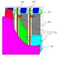
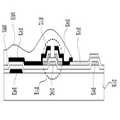
최근에 대표적인 표시장치로는 LCD 및 OLED가 있으며 OLED중에서도 AMOLED가 주류를 이루고 있다. 도 1은 LCD의 기본 구조를 도시한 도면으로서, 도 1을 참조하면 컬러필터 기판(100)에 Red/Green/Blue(110)를 표시하는 레진(resin)사이에 BM(130)이 있으며, 공통전극(120)이 ITO같은 투명전극으로 도포되어 있고 공통전극(120)에는 공통전압(미도시)이 인가되어 TFT 기판의 화소전극과의 전압에 의해 액정을 구동한다.Recently, there are LCD and OLED as representative display devices, and AMOLED is the mainstream among OLEDs. 1, there is shown a basic structure of an LCD. Referring to FIG. 1, there is a
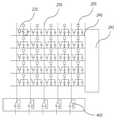
한편 하측의 기판은 TFT 기판(200)으로서, 화소전극에 화소전압을 인가하는 종방향의 소스 신호선(250) 및 TFT의 게이트 전압을 온오프시키는 횡방향의 게이트 신호선(240) 및 TFT(220)가 배치되어 있다.On the other hand, the lower substrate includes, as the
소스 신호선(250) 및 게이트 신호선(240)은 LDI(LCD Drive IC)에 접속되어 LDI 에 내장되거나 또는 분리된 TCON(Time Controller)의 작동에 의해 시분할 방법으로 LCD를 구동한다. 이때 게이트 신호선(240)은, LCD 기판 내부에 제조된 TFT에 의해 동작을 하는 GIP(Gate In Panel, 241) 방식에 의해 동작을 하기도 하며 이때 LDI는 GIP에서 필요로 하는 clock을 공급하는 역할을 한다.The
OLED는 최근에 AMOLED가 주류로 사용되고 있으며 도 2는 AMOLED에 관한 도면이다. 도 2를 참조하면, 기판(substrate)의 상면에는 화소전극에 화소전압을 인가하는 종방향의 소스 신호선(250) 및 TFT의 게이트 전압을 온오프시키는 횡방향의 게이트 신호선(240) 및 TFT(220)가 배치되어 있다.OLEDs have recently been used as mainstream AMOLEDs, and Figure 2 is a drawing of AMOLEDs. 2, a vertical
소스 신호선(source line, 250)에 인가된 화소전압은 TFT(Thin Film Transistor, 220)를 거쳐 화소전극(Anode)로 인가되고 화소전극은 홀(Hole, 정공)을 공통전극인 캐소드(Cathode)와의 사이에 있는 유기 발광체(Organic Emitter)로 주입시키고 캐소드는 일렉트론(electron, 전자)을 유기 발광체로 주입하면 유기물에서 정공과 전자의 결합에 의해 빛이 발산하며 유기발광체의 파장대별로 red/green/blue가 구분되는 표시장치이다.The pixel voltage applied to the
도 1이나 도 2의 TFT 기판을 살펴보면 구조가 동일하며 구동방법만 전압구동방식의 LCD와 전류구동방식의 OLED라는 것만이 차이가 있는 것이다.The TFT substrate of FIGS. 1 and 2 has the same structure, except that only the driving method is a voltage driven type LCD and a current driven type OLED.
본 발명에서는 편의상 LCD를 예로 들어 설명하였으나 모든 기술사상은 OLED에 동일하게 적용되며, LCD와 OLED를 총칭하여 표시장치라고 칭한다. 물론, 표시장치에는 LCD와 OLED만 있는 것은 아니며, 소스라인과 게이트라인의 구동에 의해서 TFT가 동작하고 TFT에 연결된 화소를 포함하는 모든 표시장치는, 본 발명에서 총칭하는 표시장치의 범주에 포함된다.In the present invention, an LCD is used as an example for the sake of simplicity, but all technical ideas are applied to the same OLED, and the LCD and the OLED are collectively referred to as a display device. Of course, the display device does not have only the LCD and the OLED, and all the display devices including pixels connected to the TFTs operated by the driving of the source line and the gate line are included in the category of the display device collectively referred to in the present invention .
다시 도 1을 참조하면, 도 1과 같이 컬러필터 기판(100)에 공통전극이 있는 LCD의 구조를 TN 타입이라고 하며, 횡전계 모드인 IPS나 FFS등은 컬러필터 기판에 공통전극을 필요로 하지 않는다.Referring again to FIG. 1, the structure of an LCD having a common electrode on a
본 발명의 표시장치의 화소를 터치센서로 활용하는 경우에 있어서 화소의 상면에 공통전극이 있는 경우, 공통전극의 전위가 화소와 오브젝트간의 터치정전용량(Ct)의 형성을 방해하여 터치 정전용량(Ct)이 발생하지 않으므로, TN 타입 LCD의 경우에는 TFT기판이 상측으로 올라가고 컬러필터를 하측으로 위치시켜 공통전극으로 인한 영향을 배제하는 구조에서 터치검출이 가능하다. 반면, 횡전계모드 타입의 LCD에서는, 컬러필터에 공통전극이 없으므로 본 발명의 화소를 이용한 터치센서가 LCD에 대한 별도의 조치 없이도 잘 동작하게 된다.In the case where the pixel of the display device of the present invention is used as a touch sensor, when the common electrode exists on the upper surface of the pixel, the potential of the common electrode hinders the formation of the touch capacitance Ct between the pixel and the object, Ct) is not generated. Therefore, in the case of a TN type LCD, touch detection is possible in a structure in which the TFT substrate rises to the upper side and the color filter is positioned at the lower side to eliminate the influence due to the common electrode. On the other hand, in the transverse electric field mode LCD, since there is no common electrode in the color filter, the touch sensor using the pixel of the present invention can operate well without any action on the LCD.
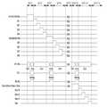
도 3은 LCD의 화소에 인가되는 전압을 생성하는 그레이 스케일 생성부(Grayscale Generator) 또는 그레이스케일 증폭부(Grayscale Amplifier) 또는 계조전압 생성부(5)이다.(이하, “계조생성부(5)”라고 한다)3 is a grayscale generator or a grayscale amplifier or a
화소에는 Red/Green/Blue등 3개를 표시하는 화소가 모여 도트를 이루며, LCD를 포함한 본 발명의 TDDI(Touch & Display Drive IC)에는 화소별 화상데이터가 외부로부터 전달된다. 화상데이터는 R/G/B에 대한 각각의 데이터를 포함하고 있으며 16bit나 18bit나 24bit등의 화상데이터가 TDDI로 전달된다. 16bit의 화상데이터의 경우에는 Red 6bit, Green 6bit, Blue 4bit의 신호가 통상적으로 사용되며 18bit의 경우에는 화소별로 각 6bit를 사용한다. 또한 24bit에는 화소별로 8bit의 데이터를 사용하므로 R+G+B는 24bit를 형성하게 된다.Pixels representing three red, green, and blue pixels are formed as dots in a pixel, and pixel-by-pixel image data is transmitted from the outside to the TDDI (Touch & Display Drive IC) of the present invention including an LCD. The image data includes respective data for R / G / B, and image data such as 16-bit, 18-bit, or 24-bit is transmitted to TDDI. In the case of 16-bit image data, red 6-bit, green 6-bit, and blue 4-bit signals are commonly used, and in the case of 18-bit, each 6-bit is used for each pixel. In addition, since 8-bit data is used for each pixel in 24-bit, R + G + B forms 24-bit.
만일 24bit의 화상데이터를 사용하게 되면 R/G/B 각각 28의 화상데이터 분포를 갖게 되며 화소에서 표출된 3가지 화소색(Pixel color)은 224의 분포를 갖게 되므로 하나의 도트는 16.7 Mega의 색분포를 갖게 된다. 또한 R/G/B를 표시하는 화소는 각각 28의 색 분포를 갖게 되는데 (28=)256 단계의 색을 표시하는 것을 “그레이스케일러, Grayscaler” 또는 “계조”라고하며 도 3의 계조생성부(5)는 외부로부터 TDDI로 입력되는 비디오 신호에 대응하여 계조전압을 만들어주는 장치이다.If the use of 24bit image data of the R / G / B each has an image data distribution of28, and three kinds of pixel color in a exposed in the pixel (Pixel color) is, so to have a distribution of224 one dot is 16.7 Mega As shown in FIG. In addition, the pixel for displaying R / G / B is there is given a color distribution of28 each(28 =) to display the color of the 256 called "gray scaler, Grayscaler" or "gradations" and gray scale production of 3 The
도 3을 참조하면, 도 3을 도트반전(Dot Inversion)을 수행하는 LCD 모드의 계조생성부(5)로서 공통전압을 사이에 두고 플러스 극성의 계조전압(또는 계조라는 용어도 동일한 의미로 사용됨)과 마이너스 극성의 계조가 있다. 이러한 계조생성부(5)는 Red/Green/Blue 별로 각각 존재하며, 하나의 색에 대해서도 플러스 극성의 계조와 마이너스 극성의 계조가 각각 존재하는 경우도 있다. 이러한 경우에 계조생성부(5)는 6개가 될 것이다.Referring to FIG. 3, the
도 3은 계조생성부(5)를 설명하기 위해 간략하게 설명한 것으로 만일 8bit의 data를 사용하는 경우라면 플러스 계조가 256개, 마이너스 계조가 256개 존재할 것이다. 도 3에서는 플러스 계조를 10개(P0~P9) 보유하며 마이너스 계조도 동일하게 10개(N0~N9) 보유하고 있다.FIG. 3 briefly explains the
도 3의 계조전압 생성부(5)를 더 설명하면 다음과 같다. 계조전압 생성부(5)에는, 후술하게 될 전압 생성부에서 만들어진 기준전압(Vdd 및 그 반대에 설치된 그라운드)이 인가된다. 그라운드 전압은 0V이외의 DC 전압이 인가될 수도 있다. 1단의 감마전압 생성부에서 만들어진 계조전압은 감마 버퍼(5a)를 통하여 버퍼링되어, 2단의 저항 스트링부(7)로 전달되어 더 세분화 된다.The
저항 스트링부(7)에서는 비디오 신호의 폭(Depth)에 맞는 계조전압을 생성한다. 예를 들어 빨강(R)의 비디오 신호의 폭(Depth)이 8bit이면 256단계의 계조전압을 생성하게 된다.The resistance string portion 7 generates a gradation voltage corresponding to the width (Depth) of the video signal. For example, if the width of the red (R) video signal is 8 bits, 256 gradation voltages are generated.
도트 인버전에서 이러한 감마전압 생성부(5)의 중심부에 위치하는 공통전압(Vcom)을 기준으로 하여 정의영역(Plus 영역, 또는 Positive 영역) 및 부의 영역(minus 영역, 또는 Negative 영역)으로 구분되며 계조전압이 공통전압보다 크면 정의영역(Plus)이며 공통전압보다 작으면 부의영역(minus)으로 정의한다.(Plus region or Positive region) and a negative region (minus region or Negative region) on the basis of the common voltage Vcom located at the center of the
TDDI의 외부에서 TDDI로 전달되는 비디오 신호(Video signal)가 빨강(R), 녹색(G), 청색(B)로 8bit 씩 인가되면, 계조전압 생성부(5)에서 이에 대응하는 계조전압이 선택된다. 예를 들어 8bit로 전달된 빨강의 비디오 데이터가 10번째를 가리키면, 도3에서 Data_P9가 선택되고, 도트 인버전의 경우에는 정의 데이터와 부의 데이터가 순차적으로 선택되므로, Data_N9도 동일한 비디오 데이터에 의해 순차적으로(in sequence) 선택된다. 또한 비디오 데이터가 244라고 하면, 비록 도 3에는 도시되어 있지 않으나 244번째 계조전압이 선택될 것이다.When a video signal transmitted from the outside of the TDDI to the TDDI is applied to the red (R), green (G) and blue (B) bits in 8 bits, the
계조부에서 선택된 전압은 소스 드라이버(Source driver)를 통하여 각 소스 신호선(source line)에 인가되고, 소스 신호선에 인가된 전압은, 활성화된 게이트 신호선(Gate line)의 TFT가 온(on) 전압에 의해, 턴 온(Turn on) 상태의 TFT에만 전달되고, 이는 화소(pixel) 및 축적 커패시터(Cst) 및 액정 커피시터(Clc)에 전달된다.The voltage selected in the gradation portion is applied to each source signal line through a source driver and the voltage applied to the source signal line is set to the on voltage of the TFT of the activated gate signal line To the TFTs in the turned-on state, which are transferred to the pixel and the storage capacitor Cst and the liquid crystal coffee sheater Clc.
화소에 인가된 계조전압은, 화소의 상측이나 좌우측에 인접한 공통전압과의 전압차(Voltage difference)에 따라, 그 사이의 액정이 반응하여 빛의 양을 조절하여 색깔별 계조(Gray scale)를 표시하게 된다.The gray scale voltages applied to the pixels are controlled by the liquid crystal between them according to the voltage difference between the upper side of the pixel and the common voltage adjacent to the left and right sides of the pixel to control the amount of light to display a gray scale .
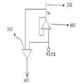
도 4는 터치를 포함하지 않은 LCD의 구동원리를 설명하는 도면이다. 도 4를 참조하면, 종방향의 소스 신호선(250)은, 소스 드라이버(source drive, 400)에 접속되어, 종 방향의 모든 TFT의 소스단자(source)에 연결되고, TFT의 게이트 단자(gate)에는 게이트 신호선(gate line, 240)이 접속되어 있다. 소스 신호선(250)에 접속된 소스 드라이버(400)는 OPAMP를 이용한 버퍼(buffer)가 사용될 수 있다. 버퍼는 입력되는 계조전압을 소스 신호선으로 출력하는 역할을 하기 때문에, input되는 계조전압을 시간지연(time delay)없이 화소로 잘 전달하며, 소스 신호선(250)에 연결된 기생 정전용량(parasitic capacitor)이나 신호선의 저항(resistance) 등을 감안한 구동능력(driving capability)이 중요하다.4 is a view for explaining a driving principle of an LCD not including a touch. 4, the
본 발명의 실시예에서 화소를 이용한 터치신호 검출 시, 소스 드라이버(400)는 하이 임피던스(High impedance, 이하 Hi-z) 상태를 유지해야 하는 별도의 기능이 필요하다. 따라서 본 발명의 소스 신호선(250)에 계조전압을 전달하는 소스 드라이버(400)는, 2가지 상태인 출력(out) 상태와 Hi-z 상태가 필요하다.In the embodiment of the present invention, when detecting a touch signal using a pixel, the
게이트 신호선(240)은 게이트 IC(미도시) 또는 GIP(Gate In Panel, 241)이 포함된 게이트 그룹에서 발원하여 횡방향의 모든 TFT의 gate에 연결된다. 화소가 많을 때는 표시장치의 좌측과 우측에 각각 gate 블록이 존재하고, 짝수 로우(row)와 홀수 로우(row)의 TFT를 구분하여 구동하거나, 화면의 왼쪽과 오른쪽의 TFT를 구분하여 구동한다. 본 발명에서는 게이트 블록이 좌측과 우측에 개별 위치하여도 도 4와 같이 하나의 블록에 위치한다고 가정한다.The
도 5는 화소를 터치 검출 센서로 사용하는 본 발명의 실시예이다. 도 5를 참조하면, 소스 드라이버(400) 내부의 소스 드라이버 출력신호는 센싱신호 처리부(Sensing signal processor, 300)로 입력된다. 센싱신호 처리부(300)는 소스 신호선의 전압 레벨(level)을 검출하는데 사용된다.Fig. 5 shows an embodiment of the present invention in which a pixel is used as a touch detection sensor. Referring to FIG. 5, a source driver output signal in the
센싱신호 처리부(300)는 소스 드라이버(400)와 같이 TDDI의 내부에 설치된다. 또는 본 발명의 표시장치의 일측에 설치되며 표시장치에 포함된 TFT를 기본소자로 하여 동작하는 것도 가능하다.The sensing
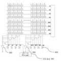
센싱신호 처리부(300)에는, 증폭기, 비교기, 버퍼(Buffer), 계조전압 연결부, 기준전압(reference) 연결부 등이 포함되어 있다. 또한 센싱신호 처리부(300)에서의 신호 처리를 위하여 TDDI에는 몇 개의 기능 블록(Function Block, 500)이 추가된다. 기능 블록(500) 내에는 CPU(510), 전원부(520), DAC(Digital to Analog Converter, 530), 타이밍부(540), 통신부(550), 메모리부(560), ADC(Analog to Digital Converter, 570), Mux(Multiplexer, 580), 로직부(590)가 포함된다.The
CPU(510)는 검출된 터치신호를 기초로 터치좌표를 연산하는 기능을 담당하며 센싱신호 처리부(300)를 운용하는데 사용될 수 있다. CPU(510)는 TDDI 내부에 존재할 수도 있으며 TDDI의 외부에 위치할 수도 있다. 전원부(520)는 센싱신호 처리부(300)에서 사용되는 전원 및 본 발명의 AC 입력전원을 생성한다.The
Timing부(540)는 검출된 터치신호를 프로세싱(processing)하는데 필요한 클럭(clock)을 생성한다. 예를 들어 하나의 ADC(570)로 여러 개의 검출된 터치신호를 디지털화(Digitizer)하기 위해서는 다음 터치신호가 검출되기 전에 완료되어야 하므로 빠른 클럭을 기반으로 신속히 디지털화가 완료되어야 할 것이다. 이때, ADC(570)의 속도를 제어하는 클럭은 타이밍부(540)에서 생성된다. 통신부(550)는 CPU가 터치좌표를 생성하는 것이 완료되면, 터치좌표를 외부로 송신하거나 외부에서 인가되는 신호를 수신하는 기능을 한다. 예를 들어 터치좌표는 I2C로 외부의 Host CPU로 전송될 것이다.The
메모리부(560)는 검출된 터치신호 데이터를 임시 저장하는 역할을 하거나 CPU의 운용에 필요한 firmware를 저장하는 역할을 한다. 휘발성의 RAM이나 Flash memory같은 비 휘발성 ROM이 사용된다. ADC(570)는 검출된 터치신호를 디지털화하여 CPU(510)가 터치좌표를 연산하는데 사용하거나 외부의 (미도시된) 호스트(host)로 전송된다. Mux(580)는 여러 개의 검출된 터치신호 중 하나를 선택하는 기능을 한다. 예를 들어 여러 개의 터치신호 처리부(300)의 신호들은 Mux(580)에 의해 하나가 선택되어 ADC(570)에서 디지털화될 것이다. 로직부(590)는 터치신호 처리부(300)나 기능블럭(500)에서 처리하는 프로세싱을 진행하며 CPU(510)도 비슷하거나 동일한 기능을 수행한다.The
도 5를 참조하여 본 발명의 실시예를 설명하면 다음과 같다. 게이트 블록에서는 순차적으로 G1->G2->G3->G4->G5->G1...의 순서로 게이트 신호선에 하나씩 약 15~20V정도 되는, TFT의 게이트(gate) 온(on) 전압이 인가되며, 게이트 온 전압이 인가되지 않은 4개의 게이트 신호선에는 약 -15~-20V 정도의 게이트 오프전압이 인가된다. 게이트 온 전압이 인가된 게이트 신호선(240)에 접속된 모든 TFT는 통전상태가 된다. 게이트 온 전압의 인가에 동기하여 소스 신호선(250)에 접속된 소스 드라이버(400)에는 계조전압이 인가된다.An embodiment of the present invention will be described with reference to FIG. In the gate block, the gate on voltage of the TFT is about 15 to 20 V, one for each gate signal line in the order of G1-> G2-> G3-> G4-> G5-> Off voltage of about -15 to -20 V is applied to the four gate signal lines to which no gate on voltage is applied. All of the TFTs connected to the
예를 들어 G1이라는 게이트 신호선에 20V의 게이트 턴 온 전압이 인가된 상황이면, G1에 접속된 횡방향의 5개의 TFT는 턴 온(Turn on) 상태가 되며, 소스 드라이버(400)로 입력되는 계조전압은 소스 드라이버(400)를 통해 소스 신호선(S1 내지 S5)으로 인가된다. 소스 신호선(S1 내지 S5)에 인가된 계조전압은, 표시장치의 화소에 화상(image)을 표시하며, 후술하게 될 TDDI의 전원전압(Power Source Voltage)으로 사용되는 AC 전원전압의 상승 또는 하강 에지(edge)에 동기하여 터치신호를 검출하는데 사용된다.For example, when a gate turn-on voltage of 20V is applied to the gate signal line G1, five TFTs in the horizontal direction connected to G1 are turned on, The voltage is applied to the source signal lines (S1 to S5) through the source driver (400). The gradation voltages applied to the source signal lines S1 to S5 indicate an image on the pixels of the display device and are used as rising or falling edges of an AC power supply voltage used as a power source voltage of a TDDI to be described later is used to detect the touch signal in synchronization with the edge.
도 6 내지 도 10은 본 발명에 따른 센싱신호 처리부(300) 구성의 실시예로, 표시장치의 화소를 이용한 터치신호 검출에 관한 본 발명의 검출 방법이다. 먼저 도 6 및 도 7을 참조하면, 증폭기(310)의 일측에는 소스 신호선(250)이 연결되고 증폭기(310)의 타측에는 소스 신호선(250)에 인가된 계조전압이 인가된다. 본 발명은 센싱신호 처리부(300)에 포함된 증폭기(310)의 일측에 연결된 소스 신호선(250)을 통해 피드백(Feedback)된 계조전압을 검출한다. 또한 본 발명의 센싱신호 처리부(300)는, (후술하는) 복수의 화소를 이용한 터치검출센서에 인가된 프리차지 전압이 피드백된 것을 검출한다.6 to 10 are embodiments of the sensing
증폭기(310)는 원래의 계조전압(original Grayscale Voltage-소스 드라이버에 인가된 계조전압)과 소스 신호선(250)에 피드백(Feedback)된 계조전압의 차이를 증폭한다.The
증폭기(310)에서 계조전압 및 일정 시간 후 피드백 된 계조전압이 증폭될 때, 계조전압은 소스 신호선(250)에 인가되는 계조전압과 동일한 상태 즉, 전원의 크기 변화가 없어야 한다.When the gradation voltage and the gradation voltage fed back after a predetermined time are amplified in the
증폭기(310)에는 두 개의 전압차이를 증폭하는 차동 증폭기(Differential Amplifier)가 사용될 수 있으며, 기타 여러 형태의 증폭기가 사용될 수 있다.A differential amplifier for amplifying two voltage differences may be used for the
증폭기(310)에서 증폭된 아날로그 전압은 도 6의 실시예와 같이 ADC(570)를 거쳐 디지털화되고 이는 도 5에 도시된 기능블럭(500)의 메모리부(560)에 수납된다. 모든 화소에 대한 터치신호 검출이 완료되어 메모리부(560)에 모든 화소의 터치 신호 검출에 관한 ADC 데이터가 수납 완료되면, 기능블럭(500)의 로직부(590)는 터치신호의 검출이 완료되었음을 CPU(510)로 전달하면, CPU(510)는 메모리부(560)에 수납된 ADC 데이터에 기초하여 터치좌표를 산출하는 것이 가능하다.The analog voltage amplified by the
그러나 ADC(570)의 사용은 TDDI의 부피를 많이 차지하며 소모전류가 크므로, 도 7과 같이 증폭기(310)의 출력은 작은 면적을 차지하는 비교기(320)의 입력으로 사용되어 비교기(320)에서 터치여부를 판단할 수 있다.However, since the use of the
도 7의 비교기(320)에는 계조전압과 피드백된 계조전압의 차이를 증폭한 신호 즉, 증폭기(310)의 출력이 입력되며, 기준전압(ref_1)이 입력된다. 비교기(320)는 증폭기(310)의 출력전압과 비교전압을 비교하여 터치여부를 판단하는 것이 가능하다. 예를 들어, 증폭기(310)에서 생성된 증폭전압은, 화소에 터치가 안되었을 때 보다 터치가 되었을 때 더 크다고 가정하면, 비교기(320)의 기준전압(ref_1)은 터치가 되었을 때의 전압과 안되었을 때의 전압의 중간에 있는 값으로 설정 할 시, 비교기(320)의 출력은 터치여부에 따라 하이나 로우를 출력하여 터치 여부를 판단하는 것이 가능하다.In the
오프젝트의 상태나 AC 전원전압의 교번 크기(swing amplitude)에 따라서 증폭기(310)에서 출력되는 전압의 크기는 달라지므로, 기준전압은 다양한 크기를 가져야 하며, TDDI는 기준전압의 크기를 변경할 수 있는 수단을 갖는다. TDDI의 레지스터의 설정으로 기준전압의 크기를 변경하는 것이 가능하다.Since the magnitude of the voltage output from the
표시장치의 모든 화소에서 터치 신호를 검출하면, 화소마다 하나의 비교기(320) 출력이 발생하며, 이러한 비교기(320) 출력은 기능 블록(500)의 메모리부(560)에 저장된다. 비교기(320)의 출력은 0이나 1의 상태를 갖는 2진수(binary)이므로, 메모리로 2비트(bit)만 할당하면 되므로, 화소 수가 많아도 메모리의 크기는 크지 않아도 될 것이다.When a touch signal is detected in all the pixels of the display device, one
도 7에서와 같이 비교기(320)를 사용할 시 비교기(320)의 출력은, 비교기로 입력되는 증폭기의 신호에 포함된 노이즈 상태에 따라 참값(True) 및 거짓값(False)을 출력하게 된다. 만일 증폭기의 출력신호에 노이즈가 많이 포함될수록 거짓값이 출력되는 빈도는 많아질 것이다. 이로 인해 잘못된 신호를 기초로 터치좌표를 산출할 시 좌표의 오류가 발생할 것이므로 이러한 오류를 줄이기 위해 비교기(320)는 두 번 또는 세 번 또는 그 이상의 복수 회(Multiple times)에 걸쳐 비교기의 출력을 임시 메모리에 저장하고 그 값을 평균하거나 참값이 일정 횟수 이상이면 참값으로 결정하는 등의 다양한 필터를 적용하여 노이즈에 강한 비교기의 출력값을 추출하는 것이 가능하다. 이를 위하여 본 발명은 비교기의 출력값을 복수 회 임시 저장할 수 있는 메모리를 포함한다.As shown in FIG. 7, when the
한편, 도 6 또는 도 7의 실시예에서, TDDI의 목적의 하나인, 표시장치로의 계조전압 전달이라는 목적을 달성하기 위해서는, 터치 검출을 위해 추가로 소모되는 시간을 최소화하는 것이 중요하다. 이를 위해 본 발명은 sample & holder(이하 S&H, 340)를 이용하여 터치 검출에 소요되는 시간을 줄이는 방안을 제시한다.On the other hand, in the embodiment of Fig. 6 or 7, in order to achieve the purpose of transferring the gradation voltage to the display device, which is one of the purposes of TDDI, it is important to minimize the additional time consumed for touch detection. To this end, the present invention proposes a method for reducing the time required for touch detection using a sample & holder (hereinafter referred to as S & H 340).
도 8을 참조하면, 소스 신호선(250)에서 피드백된 계조전압은 스위치(SW, 330)를 통하여 증폭기(310)와의 연결여부를 결정할 수 있다. 그리고 증폭기(310)와 스위치(330) 사이에는 S&H(340)가 위치하고 있다. S&H(340)는 소스 신호선(250)에서 피드백된 전압을 저장하는 저장소로서, 통상적으로 커패시터가 사용된다. 소스 신호선(250)에서 피드백된 전압이 S&H(340)에 포획(Capture)되면, 기능블록(500)의 CPU(510)나 로직부(590)는 스위치(SW, 330)를 오프시킨다. 스위치(330) 오프에 의해 센싱신호 처리부(300)에 연결된 소스 신호선(250)은 센싱신호 처리부(300)와 연결 해제된다. 이후에는 터치신호 검출에 필요한 증폭기(310)의 동작이나 비교기(320)의 동작은 소스 신호선(250)에 새로이 인가되는 계조전압과는 무관하므로, 화소에 새로운 계조전압을 인가하는 동작과 터치신호를 검출하는 프로세싱을 병행 처리할 수 있으므로, 터치 신호를 검출하는 시간을 절약하는 것이 가능하다.Referring to FIG. 8, the gradation voltage fed back from the
터치신호 검출이 완료되면, CPU(510)나 로직부(590)는 스위치(330)를 다시 턴 온(Turn on)시켜 새로이 피드백되는 계조전압을 S&H(340)에 충전시킨다. 그리고 앞에서 설명한 과정을 계속 반복한다. 이때 새로이 피드백된 소스 신호선(250)의 전압을 S&H(340)에 충전하기 이전에 기존의 전하는 방전하는 것이 바람직하다. 왜냐하면, 대다수의 LCD는 도트 인버전을 사용하므로 그 다음에 피드백 전압은 계조의 극성이 바뀌는 경우에, S&H(340)의 전하를 방전하지 않으면, 극성이 다른 계조전압이 인가됨으로 인해, 소스 신호선(250)에도 잘못된 전압이 인가되고, 이로 인해 화질불량을 유발할 수 있고, 터치 신호를 검출하기 위해 시간이 더 소요되거나 검출된 터치 신호에도 문제가 있을 수 있기 때문이다.When the touch signal detection is completed, the
그러나 액정의 동작을 위한 반전(inversion) 기법을 사용하지 않는 LCD이거나 OLED의 경우에는 S&H(340)의 전하를 굳이 방전시키기 보다는 방전시키지 않는 것이 S&H(340)의 충전시간을 절약할 수 있기 때문에 더 유리하다.However, since it is possible to save the charging time of the S &
한편, 증폭기(310)의 입력단에 설치된 S&H(340)는, 증폭기(310)의 출력단에도 설치할 수 있다. 그리고 증폭기(310)의 출력단과 S&H(340)사이에 스위치(미도시)가 설치되면 CPU(510)나 로직부(590)의 개입에 의해 스위치를 온오프 하고 S&H(340)에 저장된 전압을 기초로 터치신호 검출 및 화소전압을 운용하는 것과 무관하게 터치신호를 검출하는 것은 증폭기(310)의 입력단에 S&H(340)를 설치한 것과 동일한 효과를 갖는다. 증폭기(310) 입력단에 S&H(340)를 설치하거나 증폭기(310) 출력단에 S&H(340)를 설치하는 것은 둘 중의 하나의 방법만을 선택해야 한다.The S &
다시 도 6을 참조하면, 각 증폭기마다 ADC(570)를 사용하기 위해서는, 수천 개의 화소를 위하여 수천 개의 ADC(570)가 필요하므로, 현실적으로 TDDI에 이렇게 많은 ADC(570)를 사용하는 것은 불가능하다. 따라서 본 발명은 하나의 ADC(570)로 많은 복수 개의 증폭기(310)의 신호를 읽어 들일 수 있는 방안을 제시한다.Referring again to FIG. 6, to use the
도 11에는 기능블럭(500)에 포함된 Mux(580)가 있으며, 8개의 입력 중 하나를 선택하는 8 x 1 멀티플렉서(multiplexer)이다. 도 11을 인용하여 후술하는 mux(580)의 실시예를 참조하면, 하나의 mux(580)와 하나의 ADC(570)로 8개의 증폭기(310)의 신호를 처리할 수 있음을 설명하고 있다. 이와 같이 본 발명은 mux(580)를 이용하여 하나의 ADC(570)로 복수의 증폭기(310)의 신호를 처리하는 것이 가능하므로 ADC(570)를 최소화하여 터치신호를 처리하는 것이 가능하다.11 there is a
또한 각 증폭기(310)의 신호를 처리할 때 기능블럭(500)의 타이밍부(540)에서 생성되는 클럭을 사용하여 시분할 방법(time sharing) 방법으로 증폭기(310)의 신호를 순차적으로 처리한다. 예를 들어 8개의 증폭기(310)에 대해 1번부터 8번까지 순서를 정하고 1번 증폭기(310)의 신호를 ADC(570) 처리하고 그 다음에는 2번 증폭기의 신호를 처리하고 이외 증폭기도 동일한 방법으로 처리한다.And processes the signals of the
도 6 내지 도 7의 증폭기를 TDDI에서 설계할 때 많은 면적을 차지하므로 실제 어플리케이션에서 수천 개의 증폭기(310)가 TDDI에 내장되는 경우 TDDI의 크기가 커지는 문제가 생길 수 있다. 이러한 문제를 회피하기 위해 본 발명은 화소를 이용한 터치검출 방법에 있어서 증폭기(310)를 사용하지 않는 방법을 제시한다. 도 9는 증폭기(310)를 사용하지 않고 비교기(320)만 사용하여 터치신호를 검출하는 본 발명의 실시예이다.When the amplifier of FIGS. 6 to 7 is designed in the TDDI, it takes a lot of area. Therefore, when thousands of the
도 9를 참조하면, 계조전압을 인가하고 소정의 시간 후에 피드백된 소스 신호선(250)의 전압은 비교기(320)로 입력되며 비교기(320)에는 피드백된 전압과 비교하기 위한 기준전압(REF_GM)이 같이 인가된다. (이때 피드백된 전압은 비교기(320)에 입력되기 전에 버퍼에 입력되고 버퍼의 출력이 비교기(320)로 입력될 수 있다). 비교기(320)는 오피앰프(OPAMP)로 구현되는 것으로서, 그 동작의 원리는 당업자에게는 당연한 사실이므로 상세한 동작원리의 설명은 생략한다.9, the voltage of the
비교기(320)에 입력되는 소스 신호선(250)의 피드백 전압은, 소스 드라이버(400)에 인가되는 계조전압이 피드백된 것이다. 따라서 비교기(320)에 입력된 피드백전압은, 소스 드라이버(400)에 인가된 감마전압을 기초로 터치여부에 따라 전압의 변화가 발생한 것이다. 따라서 본 발명은 계조전압 생성부(5)를 이용하여 비교기(320)의 기준전압(REF_GM)을 생성하는 방법을 제시한다.The feedback voltage of the
터치신호를 검출하기 위하여 AC 전원전압을 교번할 때 소스 드라이버(400)의 출력은 Hi-z 상태임은 전술한 바와 같다. 따라서 비교기(320)에 입력된 피드백 전압을 유효하게 판단하는 시점에 계조전압은 화소에 전압을 인가하기 위하여 더 이상 사용되지 않는다. 따라서 터치신호 검출을 위해 비교기(320)를 사용하는 도 9 내지 10의 실시예에서 계조전압 생성부(5)를 비교기(320)의 기준전압으로 사용하는 것이 가능하다.When the AC power supply voltage is alternated to detect the touch signal, the output of the
소스 신호선(250)에서 피드백 된 계조전압은 터치유무에 따라 원래 계조전압(original gray scale voltage)보다 크기가 크거나 작을 수가 있다. 후술하겠지만, 교번하는 AC 전원전압의 상승 및 하강의 에지에 동기하여 터치신호 검출 시, 상승 및 하강여부에 따라 피드백전압의 극성이 달라진다. 이에 따라 이미 인가된 계조전압이 피드백 되었을 때, 피드백 전압과 비교하기 위한 비교전압으로서의 계조전압은, 기존 대비 크기가 커지거나 작아져야 한다.The gradation voltage fed back from the
계조전압을 비교기(320)의 기준전압으로 사용하기 위해서는 이미 인가되어 피드백된 전압과 비교해야 하므로, 계조전압이 비교전압으로 사용되기 위해 선택된 계조전압의 순번(order)에 변화가 발생하면 안된다. 예를 들어 현재 임의의 화소전극에 인가된 계조전압의 순번이, 도 3에서 Data_P8이라고 가정하면, 계조전압이 기준전압으로 사용되기 위해 Vdd나 GND등의 크기가 변화하여도 Data_P8이라는 순번은 계속 유지하고 있어야 된다는 의미이다.In order to use the gradation voltage as the reference voltage of the
* 계조전압의 크기를 변화시키는 경우를 위한 제 1의 실시예*
계조전압의 크기를 변화시키기 위한 일 실시예로, 도 3의 Data_P8의 크기가 3.0V인 경우 이를 3.1V로 상승하는 방향으로 변화시키고자 하는 경우에는, 도 3의 R1의 상측 인가된 Vdd 즉, 계조전압 생성부(5)의 기준전압(Vdd)의 크기를 크게 한다. 계조전압 생성부(5)의 기준전압은 계조전압을 만들기 위해 계조전압 생성부(5)에 인가되는 기준전압이다. 만일 계조전압의 크기를 작게 하기 위해서는 계조전압 생성부(5)의 기준전압을 낮게 인가하면 된다. 이와 같이 본 발명은 계조전압 생성부(5)의 기준전압의 크기를 달리하여 계조전압의 크기를 달리하는 수단을 제공한다.When the size of Data_P8 of FIG. 3 is 3.0V, it is desired to change the direction of the data voltage to 3.1V. In this case, Vdd applied to the upper side of R1 in FIG. 3, that is, The magnitude of the reference voltage Vdd of the gradation
또한 TDDI는 계조전압 생성부(5)의 기준전압의 크기를 변화하는 수단을 갖는다. TDDI 내부의 레지스터를 통하여 이를 수행하는 것이 가능하다.The TDDI has means for changing the magnitude of the reference voltage of the gradation
* 계조전압의 크기를 변화시키는 경우를 위한 제 2의 실시예* Second embodiment for changing the magnitude of the gradation voltage
계조전압의 크기를 변화시키기 위해서는 계조전압 생성부(5)의 기준전압과 연결되어 제 1 계조전압을 생성하는 저항의 크기를 변화시키는 방법이 있다. 도 3에서 R1내지 R10은 제 1 저항 스트링부(3)이고 제 2 계조전압을 생성하는 저항 스트링부(7)가 있다. 계조전압을 크게 하기 위해서는 제1 저항 스트링부(3)의 R1의 크기를 줄이면 된다. 또한 계조전압을 작게 하기 위해서는 R1의 크기를 크게 하면 된다.In order to change the magnitude of the gradation voltage, there is a method of changing the magnitude of the resistor which is connected to the reference voltage of the
만일 R1의 크기가 제 1 저항 스트링부(3)에 적용된 단위 저항 R을 기준으로 10R이라 할 때 1R로 줄어들면 전압 배분의 원리에 의해 Data_P8의 전압은 상승할 것이다. 또한 20R로 상승하면 Data_P8의 전압은 하락할 것이다.If the magnitude of R1 is reduced to 1R, which is 10R based on the unit resistance R applied to the first
또한 R1과 R10은 양과 부의 계조전압에 대해 동일한 역할을 하므로 R1을 줄이면 R10도 동일한 크기로 줄여줘야 한다.Also, since R1 and R10 play the same role for positive and negative gradation voltages, if R1 is reduced, R10 should be reduced to the same size.
이와 같이 본 발명은 계조 저항의 크기를 조정하여, 보다 상세하게는 제1 계조저항 스트링부의 크기를 조정하여 계조전압의 크기를 변화시키는 것이 가능하다.As described above, according to the present invention, the magnitude of the gray scale voltage can be adjusted by adjusting the magnitude of the gray scale resistor, more specifically, by adjusting the size of the first gray scale resistor string part.
한편 도 9의 실시예와 같이 계조전압 생성부(5)를 변형하여 비교기(320)의 기준전압으로 사용할 시 공통전압의 크기는 변하면 안된다. 왜냐하면 화소에 화상데이터(계조전압)를 인가하고 있는 액티브 상태의 TFT외의 TFT는 모두 TFT가 턴 오프상태로서 Cst에 충전된 충전전압과 공통전압과의 상대 전위를 이용하여 액정을 동작시키고 있는 중이므로 만일 공통전압이 변경되면 화질 이상이 발생하게 될 것이다.9, the magnitude of the common voltage should not be changed when the
따라서 본 발명은 터치 신호를 검출하기 위한 수단으로 계조전압 생성부(5)를 사용하여 계조전압을 변경시키는 경우에도 공통전압은 변경시키지 않는다.Therefore, the present invention does not change the common voltage even when the gradation
도 7은 증폭기(310) 출력을 하나의 비교기(320)로 비교하는 경우의 실시예로서 터치유무를 판단하는 것은 가능하나 터치의 정도, 즉 터치 정전용량을 형성하는 주요 인자인 터치센서(화소)와 오브젝트와의 접촉면적이나 대향거리를 판단하기 위한 정보는 부족하다. 예를 들어, 화소를 이용하여 지문인식을 하는 경우 지문의 돌출부와 지문의 침강부에 대해 터치가 되었다는 정보 외에 터치의 정도를 알아야 지문을 표시하는 것이 가능하다. 이러한 경우와 같이 터치의 정도를 확인하는 경우가 필요할 때가 있다. 이와 같이 터치의 정도는 터치센서(화소)와 오브젝트사이의 접촉면적이나 대향거리에 따라 달라지는 터치신호의 차이다.FIG. 7 shows an example of comparing the output of the
도 10은 터치의 정도를 가능하게 하는 본 발명의 실시예이다. 터치의 정도를 검출하기 위해서는 증폭기의 출력에 복수 개의 비교기(320)가 설치되며 각 비교기에는 서로 다른 비교전압(ref)이 인가된다.Figure 10 is an embodiment of the present invention which enables the degree of touch. To detect the degree of touch, a plurality of
만일 증폭기(310)에서 출력되는 전압이 터치의 정도에 따라 100mV부터 500mV 사이에 존재한다고 할 때 10개의 비교기(320)에 의해 신호차 400mV(500mV-100mV)를 10개로 구분하는 것이 가능하며 각 비교기(320)의 기준전압을 40mV의 단위로 설정하여 140mV/180mV....와 같은 기준전압에 의해 검출되는 터치 신호의 정도를 확인하는 것이 가능하다.If the voltage output from the
예를 들어 증폭기(310)에서 출력된 전압이 240mV이고 제1비교기(321)의 기준전압이 100mV부터 시작하여 제2비교기(322)의 기준전압은 140mV, 제3비교기(323)의 기준전압은 180mV, 제4비교기(324)의 기준전압은 220mV, 제5비교기(325)의 기준전압은 260mV....라고 할 때 증폭기(310)에서 출력된 240mV의 전압에 의해 제1비교기(321) 내지 제4비교기(324)의 출력과 나머지 비교기의 출력은 상태(status)가 다를 것이다. CPU(510)는 이를 참조하여 현재 증폭기(310)에서 출력되는 전압의 크기를 확인 할 수 있다.For example, when the voltage output from the
또한 본 발명은 TDDI안에 비교기(320) 그룹에 인가되는 복수 개의 기준전압을 생성하는 수단을 가지며 또한 기준전압의 크기를 변경하는 수단을 갖는다. TDDI 내부의 레지스터를 변경하여 기준전압의 크기를 변경하는 것이 가능하다. 또한 복수 개의 기준전압은 개별적으로 그 크기를 변경하는 것이 가능하다.The invention also includes means for generating a plurality of reference voltages applied to the group of
비교기(320)를 더 많이 설치할 수 있도록 증폭기(310)에서 검출되는 전압을 더 상세히 세분화 할 수 있으나 그로 인해 TDDI의 면적이 커지므로 TDDI의 원가가 상승하는 이유가 된다.The voltage detected by the
이러한 문제를 방지하기 위하여 본 발명은 도 10과 같은 기능을 하는 하나의 비교기(320) 그룹과 기능블럭(500)의 mux(580)를 활용하여 복수 개의 증폭기(310)의 터치 상태를 확인하는 방법을 제시한다.In order to prevent such a problem, the present invention is a method of checking the touch state of a plurality of
도 11은 하나의 mux(580) 및 하나의 비교기(320) 그룹으로 복수 개의 증폭기(310)의 신호를 처리하는 본 발명의 실시예이다. 도 11을 참조하면, 도 11에는 8개의 입력 신호 중 하나를 선택할 수 있는 8 x 1 mux(580)가 있으며 mux(580)에는 미도시된 기능블럭(500)의 CPU(510)로부터의 제어신호나 로직부(590)의 제어신호에 의해 8개의 입력되는 증폭기(310)의 신호 중 하나를 선택하는 것이 가능하다.11 is an embodiment of the present invention for processing signals of a plurality of
도트 인버전 방식의 LCD는 대부분 1/2/4/8/16등의 도트 인버전을 지원한다. 이는 하나의 게이트 신호선(240)에 의해 TFT의 게이트가 연결된 동일한 row에 존재하는 화소들에 대해 8도트 인버전을 예로 들면, 8개의 화소가 동일한 전위로 인버전 한다는 의미이다. 예를 들어 8 도트 인버전은, 처음 8개의 도트는 정(positive)의 인버전 그 다음의 8개의 도트는 부(negative)의 인버전, 다시 그 다음 8개는 정의 인버전을 수행하게 된다. 하나의 프레임이 완료된 후 다시 처음의 8개의 도트는 부(negative)의 인버전부터 시작하게 된다.Dot-in-version LCDs typically support dot-like versions such as 1/2/4/8/16. This means that, for example, a version with 8 dots for pixels existing in the same row to which the gate of the TFT is connected by one
동일한 인버전 즉, 동일한 정이나 부의 감마전압이 인가되어 증폭된 증폭기를 동일한 mux(580)에서 사용하는 것이 바람직하다. 그래야 비교기(320)의 기준전압의 극성이 정이나 부를 동일하게 유지하는 것이 수월하기 때문이다.It is preferable to use amplifiers amplified with the same inversion, that is, the same positive or negative gamma voltage, in the
도 11은 8개의 증폭기(310)를 하나의 mux(580) 입력으로 사용하였으며 8개의 증폭기능이 동일하게 정이나 부의 인버전을 수행하는 화소에 인가되는 소스 신호선과 연결된 증폭기(310)이다.FIG. 11 shows an
다시 도 9를 참조하면, 비교기(320)에 입력되는 피드백 신호선에도 도 8과 같이 스위치(330) 및 S&H(340)가 설치될 수 있다.Referring again to FIG. 9, the
또한 도 10의 증폭기(310)로 입력되는 피드백 신호선에도 스위치(330) 및 S&H(340)가 설치될 수 있다.The
이와 같이 본 발명은 비교기(320)나 증폭기(310)와 연결된 피드백 신호선에 스위치(330)와 S&H(340)를 설치하여 화소에 인가되는 계조전압이 좀 더 빨리 동작하게 한다.As described above, the
본 발명의 화소를 이용한 터치검출 센서 및 방법에서 화소를 이용하여 터치신호를 검출하는 방법은 TDDI에 인가되는 전원전압(Power surce)이 AC로 교번하는 전압을 인가하고 AC 전압이 상승하는 에지나 하강하는 에지에 동기하여 터치신호를 검출하는 것이다.A method of detecting a touch signal using a pixel in a touch detection sensor and a method using a pixel according to the present invention is characterized in that a power signal applied to the TDDI is applied to an AC alternating voltage, And detects the touch signal in synchronization with the edge.
도 12는 교번하는 AC 교번전압의 일 실시예이다. 도 12를 참조하면, 그라운드인 AGND를 기준으로 항상 일정한 전압차이를 유지하는 전압이 있으며 본 발명에서는 이를 Vci로 명기하였다.12 is an embodiment of an alternating AC alternating voltage. Referring to FIG. 12, there is always a voltage that maintains a constant voltage difference with respect to the ground AGND, which is defined as Vci in the present invention.
교번하는 그라운드인 AGND는 대지 그라운드(Earth GND)를 기준으로 교번(swing)하지만 AGND를 기준으로 하는 Vci는 일정한 전압을 유지하고 있으며 이러한 전압을 교번하는 AC 전압 또는 AC 전압이라고 명칭한다.AGND, which is the alternating ground, swings with respect to the ground GND. However, Vci, which is based on AGND, maintains a constant voltage, which is referred to as alternating AC voltage or AC voltage.
일예로 AC 전압은 AGND를 기준으로 항상 3V를 유지하고 있으며 AGND가 교번할 때 AGND의 크기(amplitue)만큼 Vci의 크기는 커진다. 예를 들어 AGND의 크기가 10V일 때 Vci의 크기는 13V이다.For example, the AC voltage always maintains 3V with respect to AGND. When AGND alternates, the magnitude of Vci becomes larger by AGND amplitude. For example, when AGND is 10V, the magnitude of Vci is 13V.
AC 전압이 교번할 때 절대 전위인 대지 전위를 기준으로 양(plus)의 전압에서 부(minus) 전압으로 교번할 수 있으며 부에서 양의 전압으로도 교번하며 양의 전압 내에서 교번할 수도 있으며 부의 전압 내에서만 교번하는 것이 가능하다.When AC voltage alternates, it can be alternated from plus voltage to minus voltage based on absolute potential, alternating with positive voltage, alternating within positive voltage, negative It is possible to alternate only within the voltage.
본 발명의 화소를 이용한 터치신호 검출은 화소에 계조전압을 인가하고 화소를 Hi-z 상태로 만든 후 AC 전원전압을 교번 시키고, AC 전원전압의 상승 또는 하강 에지 시 화소에서 발생하는 전압변화를 이용하여 터치신호를 검출한다.In the touch signal detection using the pixel of the present invention, the gray level voltage is applied to the pixel, the pixel is turned to the Hi-z state, the AC power source voltage is alternated, and the voltage change occurring in the pixel at the rising or falling edge of the AC power source voltage Thereby detecting the touch signal.
이러한 교번하는 전원전압은 TDDI 내부에서 생성되거나 TDDI의 외부에서 전원관리 IC인 PMIC(Power Management IC)에서 생성되어 TDDI로 인가된다. 또한 PMIC에서 생성된 AC 전압은 TDDI외에도 TCON이나 Gate IC등 본 발명의 화소를 이용한 터치검출장치에 사용되는 모든 회로물에 동일하게 적용된다.These alternate power supply voltages are generated in the TDDI or generated from a PMIC (Power Management IC), which is a power management IC outside the TDDI, and applied to the TDDI. Also, the AC voltage generated by the PMIC is applied to all the circuits used in the touch detection device using the pixel of the present invention, such as the TCON and the gate IC, in addition to the TDDI.
도 13은 본 발명의 화소를 이용한 터치검출방법에 관한 타이밍도이다. 도 5 및 도 12를 참조하여 도 13을 설명하면 다음과 같다.13 is a timing diagram related to a touch detection method using the pixel of the present invention. Referring to FIG. 5 and FIG. 12, FIG. 13 will be described as follows.
도 13은 도 5의 2개의 게이트 신호선(G1, G2)의 동작에 대해서만 설명하였으나 실제의 표시장치에서는 수백 개의 게이트 신호선이 처음부터 마지막 신호선까지 순차적으로 TFT 온 전압이 인가되는 동작을 한다. 또한 도 5의 소스 신호선(S1~S5)이 5개인 것에 대해서만 신호를 규정하였으나 실제의 표시장치에서는 수백 개에서 수천 개까지 확장된다.Although only the operation of the two gate signal lines (G1, G2) of FIG. 5 has been described with reference to FIG. 5, in an actual display device, several hundred gate signal lines are sequentially applied with the TFT-on voltage from the beginning to the last signal line. In addition, signals are defined only for five source signal lines (S1 to S5) in FIG. 5, but the actual display devices extend from hundreds to thousands.
도 12의 AC 전원전압은 TDDI의 전원전압으로 인가된다. 본 발명이 적용되지 않은 일반적인 LDI나 TDDI는 DC전압이 인가될 것이나, 본 발명에서는 AC 전원전압을 사용한다. TDDI에서 전원전압 외에 I/O(Input/Output)전원 등 추가로 전원을 필요로 하는 경우 TDDI에 인가되는 모든 전압은 AGND를 공용으로 사용하며 그 크기기 AGND와 상대적으로 결정되는 AC 전압이 인가된다.The AC power supply voltage of FIG. 12 is applied to the power supply voltage of TDDI. In general LDI or TDDI to which the present invention is not applied, a DC voltage may be applied, but an AC power supply voltage is used in the present invention. In case TDDI needs additional power such as I / O (Input / Output) power in addition to the power voltage, all voltage applied to TDDI is commonly used with AGND, and an AC voltage which is relatively determined with AGND is applied .
AC 전원전압은 TDDI에 인가되어 TDDI가 필요로 하는 전압을 전원생성부에서 생성한다.The AC power supply voltage is applied to the TDDI to generate a voltage required by the TDDI in the power generator.
도 5 및 도 13을 참조하면, 먼저 G1이 High인 구간에서 G1에 연결된 모든 TFT는 턴 온 되고, 소스 신호선(S1~S5)에는 소스 드라이버(400)가 소정의 계조전압을 인가한다. 소스 드라이버(400)의 계조전압의 인가에 따라 TFT의 화소 및 Clc, Cst의 충전이 완료되는 시점에서 CPU(510)나 로직부(590)는 소스 드라이버(400)의 출력을 Hi-z로 전환한다.5 and 13, all the TFTs connected to G1 in the period where G1 is High are turned on, and the
소스 드라이버(400)로 Hi-z로 되는 순간 화소는 도 14에 모델링된 것과 같이 Hi-z 상태가 된다. 도 14의 600은 비교기 또는 증폭기 또는 버퍼 등으로 입력이 모두 Hi-z인 소자들이 사용된다. 도 14의 저항(700)은 TFT의 턴 온 저항(Turn on resistance)로서 본 발명에서는 크기를 무시하였다.The pixel that becomes Hi-z by the
다시 도 13을 참조하면 소스 드라이버(400)가 Hi-z가 되는 시점에서 게이트는 아직 턴 온이 되어 있는 상태이고 교번하는 AC 전원전압인 Vci가 AGND와 같이 하이에서 로우나 또는 로우에서 하이로 교번(swing)한다. TDDI에 인가되는 전원전압인 Vci가 교번할 때 화소에서 검출되는 전압, 즉 도 14의 600과 화소의 교점에서 검출되는 전압은 다음과 수식과 같다.Referring again to FIG. 13, at the time when the

여기에서 Vt는 터치 검출 시 검출된 전압이며, Vgrayscale는 소스 드라이버(400)에 의해 인가된 계조전압으로서 액정 커패시터(Clc)나 스토리지 커패시터(Cst) 등에 충전된 현재의 전압이다. Cp는 화소에 연결된 소스 신호선(250)끼리의 신호선간 발생하는 기생용량이나 후술하게 될 소스 신호선(250)의 상면에 부가될 가드 레이어(Guard Layer)와 소스 신호선(250) 사이에 발생하는 기생용량 등 화소에 부가되는 기생용량(parasitic capacitor)들의 총 합이다. Clc는 액정 커패시터로서 현재 Vgrayscale로 충전되어 있으며 Vcom을 상대 그라운드로 하여 형성된다. Cst는 스토리지 커패시터로서 전단 gate 신호선(Previous gate line)을 그라운드로 하여 형성되기도 하며 이의 그라운드를 Cst_GND로 표기하였다.Here, Vt is a voltage detected at the time of touch detection, and Vgrayscale is a current voltage charged in the liquid crystal capacitor Clc, storage capacitor Cst, or the like as a gradation voltage applied by the
도 14에서 P점의 전위와 Vcom 또는 P점의 전위와 Cst_GND의 상대 크기는 일정한 DC 값이나 TDDI의 GND인 AGND가 스윙하고 있으므로 Vcom이나 Cst_GND도 대지전위인 절대 전위를 기준으로 할 시 AGND와 동일하게 스윙하고 있다.In Fig. 14, since the relative magnitude of the potential at point P, Vcom, or the point P and the Cst_GND is a constant DC value or AGND which is the GND of the TDDI swings, Vcom or Cst_GND is equal to the AGND at the ground potential I'm swinging.
[수학식 1]을 참조하면, 터치가 안되었을 때는 Ct가 형성되지 않으므로 화소에 인가되는 전압은 원래 인가된 계조전압과 동일하므로 화질의 이상 없이 표시장치에서 화상(image)을 표시하는 것이 가능하다. 그러나 화소와 손가락 같은 오브젝트 사이에 터치가 발생하면 인가된 화소에 인가된 계조전압의 변동(difference)이 발생하게 되며 전술한 바와 같이 센싱신호 처리부(300)에서 증폭기(310)나 비교기(320)를 이용하여 이러한 전압을 검출하면 터치 여부를 판단하는 것이 가능하게 된다.Referring to Equation (1), since Ct is not formed when no touch is made, the voltage applied to the pixel is the same as the originally applied gradation voltage, so that it is possible to display an image in the display device without any abnormality in image quality . However, when a touch occurs between a pixel and an object such as a finger, a difference in gradation voltage applied to the applied pixel occurs. As described above, in the sensing
다시 도 6 내지 도 7을 참조하면, 증폭기(310)의 구성으로 차동증폭기를 사용하는 경우 증폭기(310)에 사용되는 전압의 하나는 계조전압이고 하나는 피드백전압이라고 설명하였다. 차동증폭기의 출력전압은 두 개의 입력전압의 차이를 증폭하는 것으로서 다음 [수학식 2]와 같이 표시된다.Referring again to FIGS. 6 to 7, when a differential amplifier is used as the

여기에서 Vdiff는 차동증폭기의 출력전압이고 Gain은 차동증폭기에서 설정된 신호의 증폭량이고 V1은 차동증폭기의 포지티브(positive) 입력과 연결된 전압이고 V2는 네거티브 입력과 연결된 전압이다.Where Vdiff is the output voltage of the differential amplifier, Gain is the amplification of the signal set in the differential amplifier, V1 is the voltage connected to the positive input of the differential amplifier, and V2 is the voltage connected to the negative input.
현재의 계조전압이 “Vgrayscale"로 정의하였고 Gain=1이라고 가정하면 [수학식 2]는 다음의 [수학식 3]과 같이 정리할 수 있다.Assuming that the current gradation voltage is defined as " Vgrayscale " and Gain = 1, Equation (2) can be summarized as Equation (3) below.

[수학식 3]을 참조하면, 차동증폭기를 사용하여 전술한 바와 같은 방법을 사용하면 차동증폭기에서는 터치정전용량인 Ct의 부가에 따른 차이를 확인하는 것이 가능하게 된다.Referring to Equation (3), when the above-described method using a differential amplifier is used, it is possible to check the difference due to the addition of the capacitance Ct, which is the touch capacitance, in the differential amplifier.
다시 도 13을 참조하면 Vci가 교번(Swing)한 후 [수학식 2]나 [수학식 3]에 따라 검출된 전압은 ADC(570)나 비교기(320)에서 처리되어 메모리부(560)에 저장되며 CPU(510)나 로직부(590)가 이의 과정을 제어(control)할 수 있다. 또한 메모리부(560)에 저장된 신호에 근거하여 CPU(510)는 터치 좌표를 산출하고 이를 통신부(550)를 통하여 외부의 Host CPU로 전달하게 된다.Referring again to FIG. 13, the voltage detected according to Equations (2) and (3) after the Vci is swung is processed in the
또한 도 12 및 도 13을 참조하면, AC 입력전압이 하이에서 로우나 로우에서 하이로 교번하기 위해서는 교번신호가 출력되기 이전에 미리 하이나 로우의 상태에 도달해 있어야 한다. 도 13을 참조하면, 이러한 신호처리는 Vci의 스윙 이전에 이루어지며 이는 도 13에 명기하지 않았다.12 and 13, in order to alternate the AC input voltage from high to low or from low to high, it is necessary to reach the low or low state before the alternate signal is output. Referring to FIG. 13, this signal processing is performed before the swing of Vci, which is not shown in FIG.
터치 정전용량인 Ct는 다음의 [수학식 4]로 결정된다.The touch capacitance Ct is determined by the following equation (4).

여기에서 e는 유전율이며 d는 화소와 오브젝트와의 거리이며 s는 화소와 오브젝트의 접촉 면적이다. Where e is the permittivity, d is the distance between the pixel and the object, and s is the contact area between the pixel and the object.
화소의 면적이 적어도 100um2부터 수백 um2의 크기를 이루고 있고 손가락이나 터치펜 같은 오브젝트의 면적은 화소의 면적보다 상당히 크므로 S는 화소의 전체면적이라고 생각할 수 있다.Since the area of the pixel is at least 100 um2 to several hundred um2 and the area of an object such as a finger or a touch pen is much larger than the area of the pixel, S can be considered to be the entire area of the pixel.
화소의 면적이 작을 때에는 [수학식 4]에서 형성된 터치정전용량이, [수학식 1]이나 [수학식 3]의 분모에 분포한 다른 정전용량에 비해 매우 작게 되므로 터치 신호를 검출하는 것이 어려울 때도 있게 된다. 이러한 문제점을 해결하기 위하여 본 발명은 화소를 여러 개 모아서 터치를 하는 방안을 제시한다.When the area of the pixel is small, it is difficult to detect the touch signal because the touch capacitance formed in [Equation 4] is very small compared with other capacitances distributed in denominators of [Equation 1] or [Equation 3] . In order to solve such a problem, the present invention proposes a method of collecting a plurality of pixels to perform a touch.
도 15는 복수 개의 화소가 하나의 화소처럼 동작해서 하나의 터치정전용량을 형성하는 방법에 관한 본 발명의 실시예이며 도 16은 도 15에 관한 동작 타이밍도이다. 도 15 내지 도 16을 참조하면, 본 발명에 특화된 회로소자 및 회로 동작은 다음과 같다.FIG. 15 shows an embodiment of the present invention relating to a method of forming a single touch capacitance by a plurality of pixels operating as one pixel, and FIG. 16 is an operation timing diagram relating to FIG. Referring to Figs. 15 to 16, the circuit elements and circuit operation specific to the present invention are as follows.
CPU(510)나 로직부(590)의 제어신호인 “센서 블록 제어 신호(Sensor Block Control signal)”의 하이 또는 로우의 상태에 따라 소스 신호선(S1~Sm)을 센싱신호 처리부로 연결여부를 결정한다. 본 발명의 일 실시예로 센서 블록 제어 신호선의 상태가 그라운드 전위(AGND)인 0V를 로우라고 하고 5V나 10V등을 하이라고 하면, 센서 블록 제어 신호선이 하이(High, H)인 상태에서 신호선 연결스위치는 통전(Turn on)되어 소스 신호선을 센싱신호 처리부(300)로 연결한다.It is determined whether or not the source signal lines S1 to Sm are connected to the sensing signal processing unit in accordance with the high or low state of the " Sensor Block Control signal " which is the control signal of the
센서 블록 제어 신호(Bi~Bl)가 하이가 되면 S1부터 S4까지 4개의 소스 신호선이 하나의 센싱신호 처리부(300)에서 상호 연결된다. 또한 타이밍도인 도 16을 참조하면, 게이트 신호선(G1부터 G4)이 동시에 하이가 되며 이로 인해 종방향의 게이트 신호선(G1부터 G4)에 접속된 모든 TFT가 턴 온 되어 이 결과로 G1부터 G4까지 접속된 모든 TFT 중 S1부터 S4의 소스 신호선에 접속된 16개의 TFT가 모두 동시에 통전되어 센싱신호 처리부(300)에 연결되므로 이는 마치 16개의 화소가 하나의 화소와 같이 동작하는 결과를 유발하며 이로 인해 터치신호를 검출하는 화소가 넓어지고 [수학식 4]에서 도출된 터치 정전용량을 크게 하여 터치신호 검출이 용이하게 된다.When the sensor block control signals Bi to Bl are high, the four source signal lines S1 to S4 are connected to each other in one sensing
다시 도 15와 도 16을 참조하면, G1부터 G4가 턴 온 되고 센서 블록 제어신호가 하이가 되어 신호선 연결스위치가 모두 온(on) 상태가 되면 (S1~S4, G1~G4), (S5~S8, G1~G4), (S9~S12,G1~G4),...<(Sm-3~Sm, G1~G4)에 포함된 16개의 화소가 모두 연결된다. ((S1~S4, G1~G4)의 의미는 G1부터 G4가 동시에 턴 온 되었고 S1부터 S4가 하나의 그룹으로 형성되었다는 의미임).Referring again to FIGS. 15 and 16, when the signal block connecting switches G1 to G4 are turned on and the signal block control signal is turned on (S1 to S4, G1 to G4) (Sm-3 to Sm, and G1 to G4) are all connected to each other. (S1 to S4, G1 to G4 means that G1 to G4 are turned on at the same time and S1 to S4 are formed as one group).
S1부터 S4까지를 하나의 그룹으로 설정한 것은 본 발명의 실시예를 설명하기 위한 것일 뿐, 실제로는 더 작거나 더 많은 화소가 하나의 그룹으로 설정될 수 있다. 또한 G1부터 G4를 동시에 턴 온 시키는 것은 본 발명의 실시예를 설명하기 위한 것일 뿐, 실제로는 더 작거나 더 많은 게이트 신호선이 동시에 통전(turn on)될 수 있다.S1 to S4 are set as one group for explaining the embodiment of the present invention. Actually, smaller or more pixels can be set as one group. Also, turning on the gates G1 to G4 at the same time is only for explaining the embodiment of the present invention, and actually smaller or more gate signal lines can be turned on at the same time.
이러한 신호선 연결 스위치는 TDDI의 내부에 형성된다. 따라서 표시장치에는 추가되는 회로나 공정의 변경이 발생하지 않는다. 또한, 신호선 연결스위치와 센싱신호 처리부(300) 사이에는 S&H(340)가 설치될 수 있다.Such a signal line connecting switch is formed inside the TDDI. Therefore, no additional circuit or process change is caused in the display device. In addition, the S &
또한 TDDI 내부에는 신호선 연결 스위치를 제어한 신호선인 센서 블록 제어 신호선이 있으며 이는 기능블록(500)의 CPU(510)나 로직부(590)에 의해 온/오프를 반복한다. 이러한 센서 블록 제어 신호선은 상호 순차적으로 또는 상호 랜덤하게 온/오프를 반복할 수 있다. 그러나 터치 검출시간을 줄이기 위하여 동시에 턴 온 및 턴 오프를 하는 것이 더 바람직하다.In addition, the TDDI has a sensor block control signal line which is a signal line for controlling a signal line connection switch. This is repeatedly turned on / off by the
도 16을 참조하여 본 발명의 여러 개의 화소를 이용한 터치검출방법에 대하여 설명하면 다음과 같다.A touch detection method using several pixels of the present invention will be described with reference to FIG.
도 16의 영역1은 화소에 계조전압을 인가하여 이미지를 표시하는 영역2의 이전에 복수 개의 화소로 터치를 검출하는 과정이다. 상세 동작 타이밍은 다음과 같다.16 is a process of detecting a touch with a plurality of pixels before a
1.One.복수개의Plural 게이트 TFT 턴 온 전압을 동시에 인가하는 단계. Simultaneously applying a gate TFT turn-on voltage.
실시예에서는 G1부터 G4까지 4개의 게이트 신호선에 TFT 턴 온 전압을 인가하였으나 실제로는 2개 또는 10개 등 임의의 복수개의 게이트 신호선에 TFT 온 전압이 동시에 인가 될 수 있다.In the embodiment, the TFT turn-on voltage is applied to four gate signal lines from G1 to G4, but in practice, TFT on voltages can be simultaneously applied to arbitrary plural gate signal lines such as two or ten.
화상을 표시하기 위해서는 표시장치에서 오직 하나의 게이트 신호선에만 TFT 온 전압이 인가되어야 하나 본 발명은 복수개의 게이트 신호선에 TFT 온 전압을 인가한다.In order to display an image, only one gate signal line needs to be applied with a TFT-on voltage in the display device, but the present invention applies a TFT-on voltage to a plurality of gate signal lines.
복수 개의 TFT 신호선을 동시에 온 시키기 위해 TCON은 게이트 drive IC나 GIP 블록에 이러한 신호를 생성하는 클럭이나 제어신호를 인가한다. GIP에는 복수의 클럭 조합에 의해 하나의 게이트 신호선(240)이 선택되므로 상기 복수의 클럭을 변형하거나 또는 새로운 클럭을 추가하여 복수의 게이트 신호선을 선택하는 것이 가능하다.In order to turn on a plurality of TFT signal lines at the same time, the TCON applies a clock or a control signal for generating these signals to the gate drive IC or the GIP block. Since one
또한 게이트 drive IC도 복수의 클럭 조합에 의해 디코더에서 게이트 신호선을 선택하므로 상기 복수의 클럭을 변경하거나 또는 새로운 클럭을 추가하여 복수의 게이트 신호선이 선택되도록 한다.Also, the gate drive IC also selects a gate signal line from a decoder by a plurality of clock combinations, so that a plurality of gate signal lines are selected by changing the plurality of clocks or adding a new clock.
2. 소스 신호선을 이용하여 상기 1에서 턴2. Using the source signal line,온된Warm 복수의 게이트 신호선에 접속된 화소 및 화소와 연결된 커패시터에 전압( A voltage is applied to a pixel connected to a plurality of gate signal lines and a capacitor connected to a pixel프리차지전압Precharge voltage)을 인가하는 단계.).
1) 화소에는 전압이 인가되고 이후 소스 드라이버(400)가 Hi-z 및 교번하는 전원전압이 인가될 때 교번전압의 교번 에지에 동기하여 터치 신호를 검출한다. 이때 화소에 인가되는 전압은 화질과 무관한 전압이므로 이 전압을 프리차지(precharge) 전압이라고 한다.1) voltage is applied to the pixel and then the
터치신호 검출은, 교번하는 상승 또는 하강 신호 이후 소정의 시간을 기다린 이후 진행하는 것이 바람직하다. 왜냐하면 도 14에서 도시한 TFT의 온 저항(Ron) 및 Cp에 의한 신호 지연이 발생되므로 화소에서 발생한 전압의 변화가 소스 신호선(250)을 통하여 피드백 되기 위하여 일정한 시간이 필요하기 때문이다. 이때 지연 시간은 0.5us~1ms가 바람직하다. The touch signal detection preferably proceeds after waiting for a predetermined time after the alternating rising or falling signal. This is because the signal delay due to the on-resistance Ron and Cp of the TFT shown in FIG. 14 is generated, and therefore, a certain time is required for the change in the voltage generated in the pixel to be fed back through the
2) 화소에 인가되는 전압은 화소가 표시할 이미지(Image)와는 무관하므로 임의의 전압을 프리차지 전압으로 인가하는 것이 가능하다.(도 16의 영역1/3/100의 S1부터 Sm까지의 out 영역). 이때 인가된 프리차지 전압을 기초로 증폭기에서 피드백된 프리차지 전압과의 차이를 증폭한다.(2) Since the voltage applied to the pixel is independent of the image to be displayed by the pixel, it is possible to apply an arbitrary voltage to the pre-charge voltage. (Out of S1 to Sm in
본 발명의 TDDI는 이와 같은 터치검출 시 화소에 인가되는 임의의 프리차지 전압을 생성하는 수단을 갖는다. 또한 생성된 임의의 프리차지 전압의 크기를 변경하는 수단을 갖는다. TDDI 내부에 레지스터를 설정하고 레지스터의 변경에 따라 임의의 프리차지 전압의 크기를 변경하는 것이 가능하다. The TDDI of the present invention has means for generating an arbitrary pre-charge voltage to be applied to the pixel upon such touch detection. And has means for changing the magnitude of any generated pre-charge voltage. It is possible to set a register in the TDDI and change the size of an arbitrary pre-charge voltage in accordance with the change of the register.
3) 화소에 인가되는 전압은 화소가 표시할 이미지(image)와는 무관하나 1)의 임의의 프리차지 전압을 만들고 이를 운용하는 것은 전원부를 복잡하게 하므로 TDDI의 면적을 크게 하므로 바람직하지 않다. 본 발명은 계조전압 생성부(5)에서 생성된 임의의 계조전압을 프리차지 전압으로 사용하는 것이 가능하다.3) The voltage applied to the pixel is independent of the image to be displayed by the pixel, but it is undesirable to make an arbitrary pre-charge voltage of 1) and to operate it to increase the area of the TDDI. The present invention can use any gradation voltage generated by the gradation
4) 터치신호 검출을 위하여 복수의 화소에 프리차지 전압을 인가 한 후 전원전압이 교번할 때 (또는 소스 드라이버가 Hi-z 상태가 된 후) 센서 블록 제어 신호선은 하이(H) 상태가 되어 화소전압이 상호 연결될 수 있다(도 16의 영역1)4) After the pre-charge voltage is applied to the plurality of pixels for detecting the touch signal, when the power source voltage is alternated (or the source driver becomes Hi-z state), the sensor block control signal line becomes high (H) The voltages can be interconnected (
5) 터치신호 검출을 위하여 복수의 화소에 프리차지 전압을 인가 할 때, 센서 블록 제어 신호선은 하이(H) 상태가 되어 화소전압이 상호 연결될 수 있다(도 16의 영역3)5) When a pre-charge voltage is applied to a plurality of pixels for detecting a touch signal, the sensor block control signal line is in a high (H) state so that the pixel voltages can be interconnected (
3.3.터치신호를Touch signal 검출하는 단계 Detecting step
1) 화소(a pixel or pixels)에 프리차지 전압이 인가된 후 (도 16의 영역1/3/100의 S1부터 Sm까지의 out 영역) 소정의 시간이 경과되어 화소에 연결된 Cp나 Clc나 Cst나 Ct가 충전이 되면 CPU(510)나 로직부(590)는 소스 드라이버(400)를 Hi-z 상태로 전환시킨다. (도 16의 영역1/3/100)A predetermined time has elapsed after a pre-charge voltage is applied to a pixel or pixels (an out area from S1 to Sm in
2) 화소에 프리차지 전압을 인가하면서 센서 블록 제어 신호를 하이상태로 전환하여 복수의 화소가 상호 연결되도록 하는 것이 가능하다.(도 16의 영역 3)2) It is possible to switch the sensor block control signal to the high state while applying the pre-charge voltage to the pixel, so that a plurality of pixels are mutually connected. (
3) 화소에 프리차지 전압을 인가 이후 소스 드라이버(400)가 Hi-z 상태가 될 때, 센서 블록 제어 신호(Bi~Bl)를 하이상태로 전환하여 복수의 화소가 상호 연결되도록 하는 것이 가능하다.(도 16의 영역1, 영역 100)3) When the
4) 상기 2) 나 3)의 중간 시간에 어디서든지 센서 블록 제어 신호(Bi~Bl)를 턴 온 하는 것이 가능하다.4) It is possible to turn on the sensor block control signals Bi to B1 anywhere in the middle time of 2) or 3).
5) 소스 드라이버가 Hi-z가 된 후 교번하는 전원전압인 AC 입력전압(Vci)을 인가한다. 이는 도 16의 영역1/3/100의 Vci가 swing하는 영역이다.5) Apply the AC input voltage (Vci), which is the alternate power supply voltage, after the source driver becomes Hi-z. This is the area where Vci of
6) 상기 5)에서 교번하는 전원전압은 로우에서 하이로 또는 하이에서 로우로 교번한다. 로우는 하이보다 낮은 상태를 의미한다.6) The alternating power supply voltage in 5) alternates from low to high or from high to low. Low means lower than high.
7) 만일 오브젝트와 화소(pixels) 사이에 터치가 발생하여 터치 정전용량이 발생하면, 센싱신호 처리부(300)에는 복수의 서로 연결된 화소에서 발생한 수식 2에 따른 전압의 변화가 발생하며 이는 센싱신호 처리부(300)의 증폭기(310)나 비교기(320)에 의해 검출된다.7) If a touch occurs between the object and the pixels and touch capacitances are generated, the voltage of the
4. 터치 검출에 사용된 화소에 이미지를 형성하는 단계4. Step of forming an image on a pixel used for touch detection
화소의 본래 목적은 화상(image)을 표시하는 것이나 화상을 표시하기 전에 터치를 검출하기 위해 화소에는 프리차지 전압이 인가된 상태이므로 화소의 화상은 원하는 화상이 아니다. 따라서 복수의 화소(pixels)에서 터치 검출이 완료된 후 화상데이터를 각 화소별도 인가해야 한다.The original purpose of the pixel is to display an image, but since the precharge voltage is applied to the pixel to detect the touch before displaying the image, the image of the pixel is not the desired image. Therefore, after touch detection is completed on a plurality of pixels, image data must be separately applied to each pixel.
1) 서로 연결된 화소를 개별 화소로 전환하기1) Converting connected pixels to individual pixels
(1) 게이트 신호선(240)에 개별적으로 TFT 온 전압을 인가하기 : 서로 연결된 복수의 화소를 개별화소로 전환하기 위해서는 게이트 신호선(240)도 하나만 TFT 온(on) 상태를 유지해야 한다. 영역2/4/101은 게이트 신호선이 하나씩만 TFT 온 상태가 되는 하이 전압이 인가되는 것을 표시한다. 만일 101부터 104번까지의 게이트가 터치 검출을 위해 동시에 TFT 턴 온 전압이 인가된 후 터치 검출이 완료되면 101번 게이트부터 TFT 턴 온 전압이 인가되는 상태가 되고 나머지 모든 게이트는 TFT의 오프 전압이 인가된다.(1) Applying the TFT on voltage individually to the gate signal line 240: In order to switch a plurality of pixels connected to each other to individual pixels, only one
(2) 서로 연결된 소스 신호선(250)을 개별적으로 분리하기 : 서로 연결된 복수의 화소를 개별화소로 전환하기 위해서는 센서블럭(500) 제어 신호선(Bi~Bl)에 low 전압을 인가해(High 전압이 인가될 수도 있다) 턴 온 상태의 신호선 연결스위치를 모두 off 상태로 전환 시킨다. 이로 인해 소스 신호선(250)은 개별적으로 분리된다.(2) Separating the
2) 화소에 이미지 데이터를 전달하기2) Transferring image data to a pixel
상기 과정을 통해 모든 화소들은 서로 연결되지 않고 독립적으로 분리되었으므로 게이트 신호선(240)에 순차적으로 TFT 온 전압을 인가하여 계조전압을 인가하면 화소에는 화상이 표시된다. 이는 도 16의 영역 2/4/101의 영역이며, 화소에 이미지를 표시할 때에는 표시장치에서 오직 하나의 게이트 신호선(240)에만 TFT의 게이트 턴 온 전압이 인가된다.Since all the pixels are not connected to each other and are separated independently from each other, the TFT-on voltage is sequentially applied to the
5. 터치 신호 연산단계5. Touch signal operation step
복수의 화소에서 오브젝트 사이에 형성된 터치정전용량(Ct)에 의해 [수학식 2]에 따른 전압의 변화는 센싱신호처리부(300)의 증폭기(310)나 비교기(320)에서 검출되어 메모리부(560)로 전달된다. CPU(510)는 메모리의 데이터를 분석하여 터치가 발생하였는지 여부를 판단한다. 이는 터치 검출이 완료되고 화소에 이미지가 표시되는 영역(도 16의 영역2/4/101)에서 이루어진다. 또는 터치 검출이 진행되는 영역(도 16의 영역1/3/100)에서 터치 검출 및 터치신호 연산이 동시에 이루어 질 수 있다. 또는 화소에 이미지 전달이 모두 완료된 후 프레임 휴지기(Vertical front poach 및 back poach, 도 16의 영역 102)에 CPU는 메모리에 저장된 터치신호를 분석하여 터치 좌표를 연산하는 것이 가능하다.The change in voltage according to Equation (2) is detected by the
이와 같이 본 발명은 표시장치의 화소를 이용하여 터치신호 검출 및 표시장치로 사용하는 것이 가능하다.As described above, the present invention can be used as a touch signal detection and display device using pixels of a display device.
만일 터치가 안된 상태라고 하면 정밀한 터치 좌표를 추출하기 보다는 터치 여부를 판단하는 것이 선행되어야 하므로, 터치여부의 판단을 위해 전술한 터치신호 검출 및 화상표시에 관한 모든 프로세스를 진행할 필요는 없다. 예를 들어, 부분적으로 터치 검출이 가능한 영역만 터치 검출 모드(도 16의 영역1/3/101)로 진행하여 터치여부만 판단하고 터치가 검출이 되면 이후 정상적인 터치검출모드로 진입하면 효과적일 것이다.If it is determined that the touch is not performed, it is necessary to judge whether or not the touch is to be performed rather than extracting the precise touch coordinates. Therefore, it is not necessary to proceed with all processes related to the touch signal detection and image display described above for determining whether or not to touch. For example, if only an area where touch detection is possible can be performed only in the touch detection mode (
이로 인해 정상적인 터치 검출을 위해 전술한 화소들의 연결체가 100개라고 가정하면 부분적으로 50개나 25개만 가동하여 터치를 검출하는 경우 터치 검출시간이 절약되어 화소의 이미지를 표시하기 위한 시간이 더 생기며 또는 소비전류가 감소되는 효과가 있다.Assuming that the number of connected components of the above-described pixels is 100 for normal touch detection, if only 50 or 25 pieces are operated in some cases to detect the touch, the time for detecting the touch is saved, so that there is more time for displaying the image of the pixel, The current is reduced.
예를 들어 4개의 게이트 신호선 및 4개의 소스 신호선으로 형성되는 화소블럭이 있다고 가정하고 이러한 화소블럭이 터치를 검출하기 위해 액티브 상태가 되는 것을 1이라고 하고 터치검출을 하지 않는 것을 0이라고 하면 정상적인 경우의 화소를 이용한 터치검출의 상태는 아래와 같이 묘사할 수 있다.For example, if there is a pixel block formed of four gate signal lines and four source signal lines, and the pixel block is set to be in an active state for detecting a touch, The state of the touch detection using the pixel can be described as follows.
1 1 1 1 1 1 1 1 1 11 1 1 1 1 1 1 1 1 1 1
1 1 1 1 1 1 1 1 1 11 1 1 1 1 1 1 1 1 1 1
1 1 1 1 1 1 1 1 1 11 1 1 1 1 1 1 1 1 1 1
1 1 1 1 1 1 1 1 1 11 1 1 1 1 1 1 1 1 1 1
상기는 16개의 단위 화소로 이루어진 화소블럭이 횡방향으로 10개 및 종방향으로 4개 즉, 40개의 터치 검출용 화소 블록이 있음을 보여준다. 단지 터치 여부만을 검출하는 단계라면 상기는 다음과 같이 표시할 수 있다.The above shows that there are 40 pixel blocks for touch detection, that is, 10 pixel blocks composed of 16 unit pixels and 4 pixel blocks for the longitudinal direction. If it is a step of detecting only touch or not, the above can be expressed as follows.
1 1 1 1 1 1 1 1 1 11 1 1 1 1 1 1 1 1 1 1
0 0 0 0 0 0 0 0 0 00 0 0 0 0 0 0 0 0 0
1 1 1 1 1 1 1 1 1 11 1 1 1 1 1 1 1 1 1 1
0 0 0 0 0 0 0 0 0 00 0 0 0 0 0 0 0 0 0
이와 같은 조합에 의해 한 줄은 센싱하고 한 줄은 센싱하지 않으면 센싱시간은 절반으로 줄어들 것이다. 또는 한 줄은 센싱하고 두 줄은 센싱하지 않는 방법 등 다양한 방법이 제공될 수 있다.With this combination, if one line is sensed and one line is not sensed, the sensing time will be reduced to half. Or a method in which one line is sensed and two lines are not sensed.
도 15의 센싱신호 처리부(300)에는 S&H(340)가 연결될 수 있으며 상세 동작원리는 전술한 바와 같다.The S &
다시 도 16을 참조하면, 정상적으로 화소만 표시하는 표시장치는 게이트 신호선(240)이 G1부터 Gm까지 순차적으로 로우에서 하이가 인가되는 상태이다. 즉, 도 16의 영역2부터 시작해서 영역4가 이어지고 마지막으로 영역 101에서 표시장치에 이미지를 표시하는 것이 종료된다.Referring again to FIG. 16, a display device that normally displays only pixels is in a state in which the
TCON은 이러한 영상신호에 적합한 타이밍을 LDI에 제공하고 있으나 본 발명의 TCON에서는 도 16과 같이 영상신호의 전송 이전에 터치신호를 검출하는 신호를 본 발명의 TDDI로 먼저 보내주어야 한다.TCON provides the timing suitable for the video signal to the LDI. However, in the TCON of the present invention, a signal for detecting the touch signal should be sent to the TDDI of the present invention before transmission of the video signal as shown in FIG.
만일 TCON이 그러한 신호를 보내주는 것이 불가한 경우에는 TCON으로부터 영상신호를 받고 이를 TDDI의 메모리에 수납한 후 TDDI는 자체적으로 터치검출 신호 및 영상신호를 조합하여 도 16과 같은 타이밍도에 따른 프로세스를 진행한다.If it is impossible to send such a signal, the TDDI receives the video signal from the TCON and stores it in the memory of the TDDI. Then, the TDDI combines the touch detection signal and the video signal by itself to process according to the timing diagram shown in FIG. Go ahead.
다시 도 1을 참조하면, 도 1은 소스 신호선(250)이나 게이트 신호선(240)의 크기를 다소 과장하여 표현하긴 하였으나 통상의 소스 신호선이나 게이트 신호선의 선폭(line width)이 6um~10um 정도이고 화소의 폭(width)도 30um대(around 30um)의 표시장치가 있음을 감안하면 소스 신호선(250)에 손가락등과 같은 오브젝트로 터치를 해도 마치 화소에 터치가 된 것과 같은 터치 오작동에 대한 효과가 있을 수 있다.1, although the size of the
도 17은 소스 신호선(250)이 터치 검출을 안되게 하는 방안에 대한 본 발명의 실시예이다.17 is an embodiment of the present invention for a method for preventing the
도 17은 도 4 내지 도 5의 TFT의 구조에 관한 단면도이다. 도 17을 참조하면, 소스 신호선(250)의 상면에는 가드 레이어(Guard layer, 295)가 설치된다. 가드 레이어(295)는 구리, 알루미늄, CNT(Cabon Nano Tube), 메탈 메쉬(Metal mesh) 등의 금속성 물질이나 ITO나 IZO 같은 투과성 도전물질로 제조된다.17 is a sectional view showing the structure of the TFTs of Figs. 4 to 5. Fig. Referring to FIG. 17, a
가드 레이어(295)는 소스 신호선(250)의 상면에 설치되어 표시장치의 일측에서 전원과 연결된다. 가드 레이어(295)에 연결되는 전원은 TDDI에 공급되는 전원전압 즉, 교번하는 AC 전원전압을 공급하는 PMIC(Power Management IC)에서 공급하는 전원이 연결된다. 이 전원은 AGND를 포함한다. 이 전원은 AGND와는 DC를 이루고 있으나 대지전원을 기준으로 할 때에는 교번하는 전압이다.The
또한 가드 레이어에(295)는 TDDI가 공급하는 전원이 연결될 수도 있다. 예를 들어 TDDI에서 공급되는 5V의 전원과 연결되는 경우 이 전원은 AGND를 기준으로는 DC 5V이나 절대 전위인 대지 그라운드를 기준으로 할 때에는 교번하는 전압이다.Also, the power supplied from the TDDI may be connected to the
가드 레이어(295)와 소스 신호선(250) 사이에는 보호막(280)이 설치되어 있으며 보호막(280)으로 인해 소스 신호선(250)과 가드 레이어(295)는 쇼트(short)되지 않는다.A
가드 레이어(295)가 설치되면 소스 신호선(250)이 가드 레이어(295)의 하측에 있으므로 소스 신호선(250)은 외부의 손가락 같은 오브젝트와 터치 정전용량을 형성할 수 없으므로 소스 신호선(250)이 터치를 인식하는 오류를 해결하는 것이 가능하다.Since the
또한 가드 레이어(295)는 도 1의 컬러필터 기판(100)의 하측 BM 영역에 설치될 수 있다. 전술한 바와 같이 본 발명을 실시하기 위해서는 TN 타입의 LCD는 컬러필터 기판(100)에 공통전극(120)이 있고 공통전극(120)이 화소에 오브젝트 사이에 정전용량이 형성되는 것을 방해하기 때문에 TN 타입의 LCD에서는 화소를 이용한 터치 검출이 불가하다. 단, TN 타입의 LCD를 180도 회전시켜 TFT 기판이 상측에 오도록 하면 화소와 오브젝트 사이에 터치 정전용량이 형성되므로 화소를 이용한 터치 검출이 가능하다.The
다시 도 1을 참조하면, 컬러필터 기판(100)에 공통전극(120)이 없는 횡전계모드인 IPS나 FFS 방식의 LCD에서 컬러필터 기판의 BM(Black Matrix)는 컬러필터 화소(RGB) 사이의 빛샘(light leakage)을 방지하거나 TFT 기판(200)의 소스 신호선(250)이나 게이트 신호선(240)을 차폐하는 역할을 한다. 따라서 컬러필터 기판(100)의 하측에 전술한 가드 레이어(295)를 설치하되 소스 신호선(250)과 대향하도록, 소스 신호선(250)과 대향하는 BM(130)에 설치하고 가드 레이어(295)에 관한 전술의 실시예와 동일한 전압을 인가하면 된다.Referring to FIG. 1 again, in the IPS or FFS type LCD in which the
이때 가드 레이어(295)는 횡방향의 BM(130)을 통해서 서로 연결되거나 표시장치의 액티브에리어의 외측에서 서로 연결되어 가드 레이어(295)는 서로 통전하고 있다.At this time, the guard layers 295 are connected to each other through the
컬러필터 기판(100)의 하측의 종방향으로 가드 레이어(295)가 설치되는 본 발명의 실시예에서 가드 레이어(295)에 연결되는 전원은 TFT 기판(220)에서 공급되며 컬러필터와 TFT 기판이 실(seal)로 상호 연결될 시 seal에 혼합된 도전성 스페이서(Conductive spacer)에 의해 TFT 기판(200)에서 공급하는 가드 레이어용 전원이 컬러필터 기판(100)의 가드 레이어(295)로 전달되어 연결된다.The power source connected to the
소스 신호선(250)을 터치로부터 방어하는 본 발명의 또 다른 실시예는 전술한 컬러필터(110) 하측의 가드 레이어(295)를 컬러필터 기판(100)의 상측에 배치하는 것이다. 이 경우에도 컬러필터의 종방향의 BM(130) 상면에 가드 레이어(295)를 형성하고 가드 레이어(295)를 상호 통전 가능하도록 메쉬구조로 서로 연결한 후 컬러필터(110) 상면의 일측에서 전술한 가드 레이어용 전압을 인가하면 된다. 인가할 때는 FPC나 COF와 같은 연성회로 기판을 사용하여 PMIC나 TDDI로부터 발원된 전압을 인가한다.Another embodiment of the present invention in which the
TN 타입의 LCD인 경우 컬러필터에 설치된 공통전압(120) 때문에 터치를 검출하는 것이 불가하므로 이때는 TFT 기판(200)을 상측으로 하고 컬러필터 기판(100)이 하측에 가도록 LCD를 180도 회전시키고 BLU(Back Light Unit)을 컬러필터부터 조사하게 하는 구조를 통해 화소를 이용한 터치신호 검출이 가능하다.In the case of a TN-type LCD, it is impossible to detect a touch due to the
도 18은 TN이 뒤집힌 경우에 있어서 소스 신호선(250)이 터치를 감지하지 못하는 본 발명의 실시예로서 가드 레이어(295)는 소스 신호선(250)의 하측에 설치된다. 또한 소스 신호선(250)과 가드 레이어(295) 사이에는 보호층이 두 물체 사이를 절연하는 역할을 한다.18 illustrates that the
이때 하나의 마스크로는 가드 레이어(295)를 형성하고 또 하나의 마스크로는 가드 레이어(295)를 덮은 보호막(280)을 에칭 및 노출시키고 전술한 가드 레이어용 전원을 연결한다. 또는 하나의 마스크로 가드 레이어(295)를 패터닝하고 그 상면의 보호막(280)은 LCD 공정에서 사용되는 마스크를 사용하여 패터닝하고 가드 레이어(295)의 일측을 드러낸 후 이곳에 전술한 가드 레이어용 전원을 연결하는 것도 가능하다. 이러한 경우에는 LCD의 정규공정에 사용되는 마스크 외에 한 장의 마스크만 추가되므로 경제적으로 가드 레이어(295)를 형성하는 것이 가능하다.At this time, a
도 19는 소스 신호선(250) 및 게이트 신호선(240)으로 구획된 화소를 표시하였고 화소에 연결된 소스 신호선(250)의 상면이나 하면에 추가된 가드 레이어(295)를 두껍게 표시하였다. 또한 도 19는 컬러필터의 상면이나 하면에 형성되었으며 소스 신호선(250)을 가로 막는 역할을 하는 가드 레이어(295)를 형상화한 것이기도 하다.19 shows pixels partitioned by the
이와 같이 본 발명은 TFT 기판(200)에서 소스 신호선(250)의 상면이나 하면에 가드 레이어(295)를 설치하거나 컬러필터 기판(100)의 상측이나 하측에 가드 레이어(295)를 설치하여 소스 신호선(250)과 오브젝트 간에 터치가 발생하는 것을 막는 역할을 제공한다.The
이상 본 발명의 실시예로 설명하였으나, 본 발명의 기술적 사상이 상기 실시예로 한정되는 것은 아니며, 본 발명의 기술적 사상을 벗어나지 않는 범주에서 다양한 방법으로 구현할 수 있다.While the present invention has been described in connection with what is presently considered to be the most practical and preferred embodiment, it is to be understood that the invention is not limited to the disclosed embodiments, but, on the contrary, is intended to cover various modifications and equivalent arrangements included within the spirit and scope of the invention.
5 : 계조생성부5a : 감마 버퍼
3, 7 : 저항스트링부100 : 컬러필터 기판
110 : 컬러필터120 : 공통전극
130 : BM200, 210 : TFT 기판
220 : TFT230 : 화소전극
240 : 게이트 신호선250 : 소스 신호선
260 : 드레인전극270 : 소스전극
280 : 보호막295 : 가드 레이어
300 : 센싱신호 처리부310 : 증폭기
320 : 비교기400 : 소스 드라이버
500 : 기능블록510 : CPU
520 : 전원부530 : DAC
540 : 타이밍부550 : 통신부
560 : 메모리부570 : ADC
580 : MUX590 : 로직부5:
3, 7: resistor string part 100: color filter substrate
110: color filter 120: common electrode
130:
220: TFT 230: pixel electrode
240: gate signal line 250: source signal line
260: drain electrode 270: source electrode
280: Protective layer 295: Guard layer
300: sensing signal processor 310: amplifier
320: comparator 400: source driver
500: function block 510: CPU
520: Power supply unit 530: DAC
540: Timing unit 550:
560: memory unit 570: ADC
580: MUX 590: Logic section
Claims (2)
Translated fromKorean소스 신호선에 인가한 상기 계조 전압의 피드백 전압에 기초하여 터치신호를 검출하는 센싱신호 처리부를 포함하는 것을 특징으로 하는 표시장치의 화소를 이용한 터치 검출 센서.
A gradation voltage generator for applying a gradation voltage to the source signal line and
And a sensing signal processor for detecting a touch signal based on a feedback voltage of the gradation voltage applied to the source signal line.
(b) 센싱신호 처리부를 이용하여, 상기 계조 전압의 피드백 전압에 기초하여 터치신호를 검출하는 단계를 포함하는 것을 특징으로 하는 표시장치의 화소를 이용한 터치 검출 방법.(a) applying a gradation voltage to a source signal line using a gradation voltage generator and
(b) detecting a touch signal based on a feedback voltage of the gradation voltage using a sensing signal processing unit.
Priority Applications (5)
| Application Number | Priority Date | Filing Date | Title |
|---|---|---|---|
| KR1020150179330AKR102412372B1 (en) | 2015-12-15 | 2015-12-15 | Touch sensor and touch detect method using pixel or pixels in display devices |
| US15/375,025US10540028B2 (en) | 2015-12-15 | 2016-12-09 | Touch detecting apparatus and touch detecting method using pixel or pixels in display devices |
| US15/375,011US10474261B2 (en) | 2015-12-15 | 2016-12-09 | Touch detecting apparatus and touch detecting method using pixel or pixels in display devices |
| CN201611149399.5ACN106886329B (en) | 2015-12-15 | 2016-12-13 | Touch detection apparatus and method using one or more pixels in display device |
| CN201611151397.XACN106886330B (en) | 2015-12-15 | 2016-12-13 | Touch detection apparatus and method using one or more pixels in display device |
Applications Claiming Priority (1)
| Application Number | Priority Date | Filing Date | Title |
|---|---|---|---|
| KR1020150179330AKR102412372B1 (en) | 2015-12-15 | 2015-12-15 | Touch sensor and touch detect method using pixel or pixels in display devices |
Publications (2)
| Publication Number | Publication Date |
|---|---|
| KR20170071241Atrue KR20170071241A (en) | 2017-06-23 |
| KR102412372B1 KR102412372B1 (en) | 2022-06-24 |
Family
ID=59020529
Family Applications (1)
| Application Number | Title | Priority Date | Filing Date |
|---|---|---|---|
| KR1020150179330AActiveKR102412372B1 (en) | 2015-12-15 | 2015-12-15 | Touch sensor and touch detect method using pixel or pixels in display devices |
Country Status (3)
| Country | Link |
|---|---|
| US (2) | US10540028B2 (en) |
| KR (1) | KR102412372B1 (en) |
| CN (2) | CN106886329B (en) |
Cited By (1)
| Publication number | Priority date | Publication date | Assignee | Title |
|---|---|---|---|---|
| WO2022173148A3 (en)* | 2021-02-13 | 2022-10-06 | 이성호 | Method for improving sensitivity by using shielding capacity with remodeled parasitic capacity |
Families Citing this family (11)
| Publication number | Priority date | Publication date | Assignee | Title |
|---|---|---|---|---|
| JP2017167426A (en)* | 2016-03-17 | 2017-09-21 | セイコーエプソン株式会社 | Electro-optical device and electronic apparatus |
| JP6702284B2 (en)* | 2017-09-05 | 2020-06-03 | 株式会社デンソー | Liquid crystal panel drive circuit and liquid crystal display device |
| KR20190033235A (en)* | 2017-09-21 | 2019-03-29 | 삼성전자주식회사 | Gamma circuit supporting optical fingerprint recognition, electronic device including the same and method of performing optical fingerprint recognition |
| CN110147167B (en)* | 2018-02-11 | 2022-05-24 | 奇景光电股份有限公司 | Touch display driving circuit, operation circuit, display device and operation method thereof |
| CN108470539B (en)* | 2018-06-13 | 2020-04-21 | 京东方科技集团股份有限公司 | Pixel circuit and driving method thereof, display panel and display device |
| KR102591836B1 (en)* | 2018-09-11 | 2023-10-20 | 엘지디스플레이 주식회사 | Touch display panel, touch display device |
| CN109860271B (en)* | 2019-04-16 | 2021-03-02 | 京东方科技集团股份有限公司 | Display panel, reading circuit thereof and display terminal |
| US11521526B2 (en)* | 2019-09-03 | 2022-12-06 | Synaptics Incorporated | Device and method for testing interconnection of display module |
| US10928944B1 (en)* | 2019-11-22 | 2021-02-23 | Synaptics Incorporated | Device and method for proximity sensing on an input device |
| CN113447858B (en)* | 2020-11-11 | 2022-11-11 | 重庆康佳光电技术研究院有限公司 | Circuit backboard detection device and detection method |
| CN120108354B (en)* | 2025-05-09 | 2025-07-29 | 惠科股份有限公司 | Data driving circuit, driving module and display device |
Citations (2)
| Publication number | Priority date | Publication date | Assignee | Title |
|---|---|---|---|---|
| KR20070118797A (en)* | 2006-06-13 | 2007-12-18 | 삼성전자주식회사 | LCD and its driving method |
| KR20130143415A (en)* | 2012-06-21 | 2013-12-31 | 엘지디스플레이 주식회사 | Touch sensing apparatus and driving method thereof |
Family Cites Families (13)
| Publication number | Priority date | Publication date | Assignee | Title |
|---|---|---|---|---|
| KR20070033532A (en)* | 2005-09-21 | 2007-03-27 | 삼성전자주식회사 | Display device with touch sensing function, its driving device and sensing signal processing method |
| WO2008068920A1 (en)* | 2006-12-06 | 2008-06-12 | Sharp Kabushiki Kaisha | Gradation voltage correction system and display apparatus utilizing the same |
| US8040326B2 (en)* | 2007-06-13 | 2011-10-18 | Apple Inc. | Integrated in-plane switching display and touch sensor |
| JP5602390B2 (en)* | 2008-08-19 | 2014-10-08 | 富士フイルム株式会社 | Thin film transistor, active matrix substrate, and imaging device |
| JP2010108501A (en)* | 2008-10-30 | 2010-05-13 | Samsung Electronics Co Ltd | Touch screen controller having increased sensing sensitivity, and display driving circuit and display device and system having the touch screen controller |
| KR101230196B1 (en)* | 2010-10-29 | 2013-02-06 | 삼성디스플레이 주식회사 | Liquid Crystal Display having a Touch Screen Panel |
| KR101670402B1 (en)* | 2011-10-30 | 2016-10-28 | 이용만 | Display and touch panels with drive and sense techniques |
| KR20140032252A (en)* | 2012-09-06 | 2014-03-14 | 한국전자통신연구원 | Display for touch screen and manufacturing method of the same |
| KR101444580B1 (en)* | 2013-02-13 | 2014-09-25 | 삼성전기주식회사 | Apparatus for sensing capacitance and touchscreen apparatus |
| US20150070323A1 (en)* | 2013-09-10 | 2015-03-12 | Qualcomm Incorporated | Display-to-display data transmission |
| US20150212643A1 (en)* | 2014-01-27 | 2015-07-30 | Samsung Electronics Co., Ltd. | Touch sensing controller, touch sensing device and touch sensing system including the same |
| KR102171259B1 (en)* | 2014-06-10 | 2020-10-29 | 삼성전자 주식회사 | Liquid crystal display device for improving crosstalk characteristic |
| KR102297485B1 (en)* | 2015-01-13 | 2021-09-02 | 삼성디스플레이 주식회사 | Method for driving touch screen panel |
- 2015
- 2015-12-15KRKR1020150179330Apatent/KR102412372B1/enactiveActive
- 2016
- 2016-12-09USUS15/375,025patent/US10540028B2/enactiveActive
- 2016-12-09USUS15/375,011patent/US10474261B2/enactiveActive
- 2016-12-13CNCN201611149399.5Apatent/CN106886329B/enactiveActive
- 2016-12-13CNCN201611151397.XApatent/CN106886330B/enactiveActive
Patent Citations (2)
| Publication number | Priority date | Publication date | Assignee | Title |
|---|---|---|---|---|
| KR20070118797A (en)* | 2006-06-13 | 2007-12-18 | 삼성전자주식회사 | LCD and its driving method |
| KR20130143415A (en)* | 2012-06-21 | 2013-12-31 | 엘지디스플레이 주식회사 | Touch sensing apparatus and driving method thereof |
Cited By (2)
| Publication number | Priority date | Publication date | Assignee | Title |
|---|---|---|---|---|
| WO2022173148A3 (en)* | 2021-02-13 | 2022-10-06 | 이성호 | Method for improving sensitivity by using shielding capacity with remodeled parasitic capacity |
| US12074610B2 (en) | 2021-02-13 | 2024-08-27 | Sung Ho Lee | To improve sensitivity by using a modified shielding capacity of parasitic capacity |
Also Published As
| Publication number | Publication date |
|---|---|
| US10474261B2 (en) | 2019-11-12 |
| CN106886330B (en) | 2020-03-31 |
| KR102412372B1 (en) | 2022-06-24 |
| CN106886329A (en) | 2017-06-23 |
| CN106886329B (en) | 2020-03-31 |
| CN106886330A (en) | 2017-06-23 |
| US20170168623A1 (en) | 2017-06-15 |
| US20170168624A1 (en) | 2017-06-15 |
| US10540028B2 (en) | 2020-01-21 |
Similar Documents
| Publication | Publication Date | Title |
|---|---|---|
| KR102412372B1 (en) | Touch sensor and touch detect method using pixel or pixels in display devices | |
| EP3130987B1 (en) | Touch sensor integrated display device and method for driving the same | |
| US10488964B2 (en) | Touch display device, method for driving the same, driving circuit, data-driving circuit, and gate-driving circuit | |
| EP3128401B1 (en) | Touch sensor integrated display device and method for driving the same | |
| US10620749B2 (en) | Display device having embedded touch screen and method for detecting touch to prevent a signal line from being observed and remove an influence of a touch sensor | |
| EP3125226B1 (en) | Touch sensor integrated display device and method for driving the same | |
| EP3040971B1 (en) | Oled display device | |
| US20170108970A1 (en) | Display Device Having Touch Sensor and Driving Method Thereof | |
| US10386973B2 (en) | Display device having a guard layer configured to prevent interference of signals between a touch screen and a signal line, and method of manufacturing the same | |
| KR102412369B1 (en) | Display device integrated with touch screen | |
| US20160092027A1 (en) | Touch sensing device and driving method thereof | |
| US11836311B2 (en) | Display device and data driver | |
| US10802654B2 (en) | Touch display device, driving circuit, and driving method | |
| KR20160087467A (en) | Method for driving touch screen panel | |
| US10254891B2 (en) | Touch sensitive display device having resistance to noise, and control methods therefor | |
| CN104777950A (en) | Touch screen and related touch sensing control circuit | |
| KR101968271B1 (en) | Display device having touch screen function | |
| KR102743875B1 (en) | Touch signal detection device using a multiplexor | |
| KR102416750B1 (en) | Organic light emitting display device and the method for driving the same | |
| KR20200141782A (en) | Touch driving circuit, touch controller and touch display device | |
| KR20170080344A (en) | Display apparatus with integrated touch screen comprising the same | |
| KR102262841B1 (en) | Organic light emitting display panel, organic light emitting display device, and the method for driving the organic light emitting display device | |
| KR20170079499A (en) | Touch power driving circuit and display apparatus with integrated touch screen comprising the same | |
| KR20160078692A (en) | Organic light emitting display device and method for the same | |
| EP4394753A1 (en) | Display device |
Legal Events
| Date | Code | Title | Description |
|---|---|---|---|
| PA0109 | Patent application | Patent event code:PA01091R01D Comment text:Patent Application Patent event date:20151215 | |
| PG1501 | Laying open of application | ||
| PA0201 | Request for examination | Patent event code:PA02012R01D Patent event date:20201016 Comment text:Request for Examination of Application Patent event code:PA02011R01I Patent event date:20151215 Comment text:Patent Application | |
| E902 | Notification of reason for refusal | ||
| PE0902 | Notice of grounds for rejection | Comment text:Notification of reason for refusal Patent event date:20220125 Patent event code:PE09021S01D | |
| E701 | Decision to grant or registration of patent right | ||
| PE0701 | Decision of registration | Patent event code:PE07011S01D Comment text:Decision to Grant Registration Patent event date:20220330 | |
| GRNT | Written decision to grant | ||
| PR0701 | Registration of establishment | Comment text:Registration of Establishment Patent event date:20220620 Patent event code:PR07011E01D | |
| PR1002 | Payment of registration fee | Payment date:20220621 End annual number:3 Start annual number:1 | |
| PG1601 | Publication of registration |