KR20170068073A - Driving circuit for display device with touch - Google Patents
Driving circuit for display device with touchDownload PDFInfo
- Publication number
- KR20170068073A KR20170068073AKR1020150174827AKR20150174827AKR20170068073AKR 20170068073 AKR20170068073 AKR 20170068073AKR 1020150174827 AKR1020150174827 AKR 1020150174827AKR 20150174827 AKR20150174827 AKR 20150174827AKR 20170068073 AKR20170068073 AKR 20170068073A
- Authority
- KR
- South Korea
- Prior art keywords
- touch
- gate
- clock
- signal
- supplied
- Prior art date
- Legal status (The legal status is an assumption and is not a legal conclusion. Google has not performed a legal analysis and makes no representation as to the accuracy of the status listed.)
- Withdrawn
Links
Images


Classifications
- G—PHYSICS
- G09—EDUCATION; CRYPTOGRAPHY; DISPLAY; ADVERTISING; SEALS
- G09G—ARRANGEMENTS OR CIRCUITS FOR CONTROL OF INDICATING DEVICES USING STATIC MEANS TO PRESENT VARIABLE INFORMATION
- G09G3/00—Control arrangements or circuits, of interest only in connection with visual indicators other than cathode-ray tubes
- G09G3/20—Control arrangements or circuits, of interest only in connection with visual indicators other than cathode-ray tubes for presentation of an assembly of a number of characters, e.g. a page, by composing the assembly by combination of individual elements arranged in a matrix no fixed position being assigned to or needed to be assigned to the individual characters or partial characters
- G—PHYSICS
- G06—COMPUTING OR CALCULATING; COUNTING
- G06F—ELECTRIC DIGITAL DATA PROCESSING
- G06F3/00—Input arrangements for transferring data to be processed into a form capable of being handled by the computer; Output arrangements for transferring data from processing unit to output unit, e.g. interface arrangements
- G06F3/01—Input arrangements or combined input and output arrangements for interaction between user and computer
- G06F3/03—Arrangements for converting the position or the displacement of a member into a coded form
- G06F3/041—Digitisers, e.g. for touch screens or touch pads, characterised by the transducing means
- G06F3/0416—Control or interface arrangements specially adapted for digitisers
- G—PHYSICS
- G09—EDUCATION; CRYPTOGRAPHY; DISPLAY; ADVERTISING; SEALS
- G09G—ARRANGEMENTS OR CIRCUITS FOR CONTROL OF INDICATING DEVICES USING STATIC MEANS TO PRESENT VARIABLE INFORMATION
- G09G3/00—Control arrangements or circuits, of interest only in connection with visual indicators other than cathode-ray tubes
- G09G3/20—Control arrangements or circuits, of interest only in connection with visual indicators other than cathode-ray tubes for presentation of an assembly of a number of characters, e.g. a page, by composing the assembly by combination of individual elements arranged in a matrix no fixed position being assigned to or needed to be assigned to the individual characters or partial characters
- G09G3/22—Control arrangements or circuits, of interest only in connection with visual indicators other than cathode-ray tubes for presentation of an assembly of a number of characters, e.g. a page, by composing the assembly by combination of individual elements arranged in a matrix no fixed position being assigned to or needed to be assigned to the individual characters or partial characters using controlled light sources
- G09G3/30—Control arrangements or circuits, of interest only in connection with visual indicators other than cathode-ray tubes for presentation of an assembly of a number of characters, e.g. a page, by composing the assembly by combination of individual elements arranged in a matrix no fixed position being assigned to or needed to be assigned to the individual characters or partial characters using controlled light sources using electroluminescent panels
- G09G3/32—Control arrangements or circuits, of interest only in connection with visual indicators other than cathode-ray tubes for presentation of an assembly of a number of characters, e.g. a page, by composing the assembly by combination of individual elements arranged in a matrix no fixed position being assigned to or needed to be assigned to the individual characters or partial characters using controlled light sources using electroluminescent panels semiconductive, e.g. using light-emitting diodes [LED]
- G09G3/3208—Control arrangements or circuits, of interest only in connection with visual indicators other than cathode-ray tubes for presentation of an assembly of a number of characters, e.g. a page, by composing the assembly by combination of individual elements arranged in a matrix no fixed position being assigned to or needed to be assigned to the individual characters or partial characters using controlled light sources using electroluminescent panels semiconductive, e.g. using light-emitting diodes [LED] organic, e.g. using organic light-emitting diodes [OLED]
- G09G3/3266—Details of drivers for scan electrodes
- G—PHYSICS
- G09—EDUCATION; CRYPTOGRAPHY; DISPLAY; ADVERTISING; SEALS
- G09G—ARRANGEMENTS OR CIRCUITS FOR CONTROL OF INDICATING DEVICES USING STATIC MEANS TO PRESENT VARIABLE INFORMATION
- G09G3/00—Control arrangements or circuits, of interest only in connection with visual indicators other than cathode-ray tubes
- G09G3/20—Control arrangements or circuits, of interest only in connection with visual indicators other than cathode-ray tubes for presentation of an assembly of a number of characters, e.g. a page, by composing the assembly by combination of individual elements arranged in a matrix no fixed position being assigned to or needed to be assigned to the individual characters or partial characters
- G09G3/34—Control arrangements or circuits, of interest only in connection with visual indicators other than cathode-ray tubes for presentation of an assembly of a number of characters, e.g. a page, by composing the assembly by combination of individual elements arranged in a matrix no fixed position being assigned to or needed to be assigned to the individual characters or partial characters by control of light from an independent source
- G09G3/36—Control arrangements or circuits, of interest only in connection with visual indicators other than cathode-ray tubes for presentation of an assembly of a number of characters, e.g. a page, by composing the assembly by combination of individual elements arranged in a matrix no fixed position being assigned to or needed to be assigned to the individual characters or partial characters by control of light from an independent source using liquid crystals
- G09G3/3611—Control of matrices with row and column drivers
- G09G3/3674—Details of drivers for scan electrodes
- G09G3/3677—Details of drivers for scan electrodes suitable for active matrices only
- G—PHYSICS
- G09—EDUCATION; CRYPTOGRAPHY; DISPLAY; ADVERTISING; SEALS
- G09G—ARRANGEMENTS OR CIRCUITS FOR CONTROL OF INDICATING DEVICES USING STATIC MEANS TO PRESENT VARIABLE INFORMATION
- G09G3/00—Control arrangements or circuits, of interest only in connection with visual indicators other than cathode-ray tubes
- G09G3/20—Control arrangements or circuits, of interest only in connection with visual indicators other than cathode-ray tubes for presentation of an assembly of a number of characters, e.g. a page, by composing the assembly by combination of individual elements arranged in a matrix no fixed position being assigned to or needed to be assigned to the individual characters or partial characters
- G09G3/34—Control arrangements or circuits, of interest only in connection with visual indicators other than cathode-ray tubes for presentation of an assembly of a number of characters, e.g. a page, by composing the assembly by combination of individual elements arranged in a matrix no fixed position being assigned to or needed to be assigned to the individual characters or partial characters by control of light from an independent source
- G09G3/36—Control arrangements or circuits, of interest only in connection with visual indicators other than cathode-ray tubes for presentation of an assembly of a number of characters, e.g. a page, by composing the assembly by combination of individual elements arranged in a matrix no fixed position being assigned to or needed to be assigned to the individual characters or partial characters by control of light from an independent source using liquid crystals
- G09G3/3611—Control of matrices with row and column drivers
- G09G3/3696—Generation of voltages supplied to electrode drivers
- G—PHYSICS
- G09—EDUCATION; CRYPTOGRAPHY; DISPLAY; ADVERTISING; SEALS
- G09G—ARRANGEMENTS OR CIRCUITS FOR CONTROL OF INDICATING DEVICES USING STATIC MEANS TO PRESENT VARIABLE INFORMATION
- G09G2310/00—Command of the display device
- G09G2310/08—Details of timing specific for flat panels, other than clock recovery
- G—PHYSICS
- G09—EDUCATION; CRYPTOGRAPHY; DISPLAY; ADVERTISING; SEALS
- G09G—ARRANGEMENTS OR CIRCUITS FOR CONTROL OF INDICATING DEVICES USING STATIC MEANS TO PRESENT VARIABLE INFORMATION
- G09G2330/00—Aspects of power supply; Aspects of display protection and defect management
- G09G2330/02—Details of power systems and of start or stop of display operation
- G09G2330/028—Generation of voltages supplied to electrode drivers in a matrix display other than LCD
Landscapes
- Engineering & Computer Science (AREA)
- Theoretical Computer Science (AREA)
- Physics & Mathematics (AREA)
- General Physics & Mathematics (AREA)
- Computer Hardware Design (AREA)
- General Engineering & Computer Science (AREA)
- Chemical & Material Sciences (AREA)
- Crystallography & Structural Chemistry (AREA)
- Human Computer Interaction (AREA)
- Control Of Indicators Other Than Cathode Ray Tubes (AREA)
Abstract
Translated fromKoreanDescription
Translated fromKorean본 발명은 타이밍 컨트롤러의 출력 신호들의 수 증가없이 디스플레이 구동 기간과 터치 센싱 기간에 서로 다른 제어 신호를 게이트 구동 회로에 공급할 수 있는 터치 겸용 디스플레이 장치용 구동 회로에 관한 것이다.The present invention relates to a driving circuit for a touch-sensitive display device capable of supplying a different control signal to a gate driving circuit during a display driving period and a touch sensing period without increasing the number of output signals of the timing controller.
디스플레이의 화면상에서 터치로 정보 입력이 가능한 터치 센서는 스마트 폰과 같은 휴대용 정보 기기뿐만 아니라 노트북, 모니터, 가전 제품 등의 다양한 디스플레이에 확대 적용되고 있다.The touch sensor capable of inputting information by touch on the screen of the display is being applied not only to portable information devices such as a smart phone but also to various displays such as a notebook computer, a monitor, and a home appliance.
디스플레이에 적용된 터치 기술은 터치 센서의 위치에 따라 애드 온(Add on) 타입과 인 셀(In-cell) 타입으로 나누어진다. 애드 온 타입은 터치 스크린 패널을 디스플레이 패널 위에 부착한 외장형 방식이고, 인 셀 타입은 터치 전극을 디스플레이 패널에 내장함으로써 디스플레이 패널과 터치 스크린을 일체화한 내장형 방식이다.The touch technology applied to the display is divided into an add-on type and an in-cell type depending on the position of the touch sensor. The add-on type is an external type in which a touch screen panel is mounted on a display panel, and the in-cell type is a built-in type in which a display panel and a touch screen are integrated by incorporating a touch electrode in a display panel.
인 셀 타입은 디스플레이 장치의 슬림화를 위하여 더욱 진보되어 액정 디스플레이의 공통 전극을 분할하여 터치 전극으로 활용하는 어드밴스드 인 셀 터치(Advanced In-cell Touch; 이하 AIT) 디스플레이 장치로 발전되고 있다.In-cell type is being developed as an Advanced In-cell Touch (AIT) display device which is further advanced for slimming down a display device and divides a common electrode of a liquid crystal display into a touch electrode.
AIT 디스플레이 장치를 포함하는 인 셀 터치 디스플레이 장치는 픽셀들과 터치 센서들의 커플링(Coupling)으로 인한 상호 영향을 줄이기 위하여, 각 프레임 기간을 픽셀들을 다수의 블록으로 분할 구동하는 다수의 디스플레이 구동 기간과, 다수의 터치 센싱 기간으로 시분할하고, 디스플레이 구동 기간과 터치 센싱 기간이 교번하도록 터치 겸용 디스플레이 패널을 구동한다.An in-cell touch display device including an AIT display device includes a plurality of display driving periods for dividing each frame period into a plurality of blocks to reduce mutual influences due to coupling of pixels and touch sensors, Divides the time into a plurality of touch sensing periods, and drives the touch-compatible display panel so that the display driving period and the touch sensing period are alternated.
디스플레이 구동 기간에서 게이트 구동 회로는 해당 블록의 게이트 라인들을 순차 구동해야 하고, 디스플레이 구동 기간들 사이의 터치 센싱 기간에서 게이트 구동 회로는 시퀀셜(Sequential) 회로 특성을 유지해야 한다. 이를 위하여, 게이트 구동 회로는 디스플레이 구동 기간과 터치 센싱 기간에서 서로 다른 제어 신호를 필요로 한다.In the display driving period, the gate driving circuit must sequentially drive the gate lines of the corresponding block, and in the touch sensing period between the display driving periods, the gate driving circuit should maintain the sequential circuit characteristic. To this end, the gate driving circuit requires different control signals in the display driving period and the touch sensing period.
이를 위하여, 타이밍 컨트롤러는 디스플레이 구동 기간과 터치 센싱 기간에서 요구되는 서로 다른 제어 신호들을 생성하여 공급해야 한다. 이로 인하여, 타이밍 컨트롤러의 출력핀 수가 증가되어야 하고, 인쇄 회로 기판 상의 신호 라인 수와 그에 따른 라우팅 면적이 증가되어야 하므로, 코스트 상승의 문제가 있다.To this end, the timing controller must generate and supply different control signals required in the display driving period and the touch sensing period. As a result, the number of output pins of the timing controller must be increased, and the number of signal lines on the printed circuit board and the corresponding routing area must be increased.
본 발명은 타이밍 컨트롤러의 출력 신호들의 수 증가없이 디스플레이 구동 기간과 터치 센싱 기간에 서로 다른 제어 신호를 게이트 구동 회로에 공급할 수 있는 터치 겸용 디스플레이 장치용 구동 회로를 제공한다.The present invention provides a driving circuit for a touch-sensitive display device capable of supplying a different control signal to a gate driving circuit during a display driving period and a touch sensing period without increasing the number of output signals of the timing controller.
본 발명의 한 실시예에 따른 터치 겸용 디스플레이 장치용 구동 회로는 게이트 구동부, 타이밍 컨트롤러, 전원 관리 회로를 구비한다.A driving circuit for a touch-sensitive display device according to an embodiment of the present invention includes a gate driver, a timing controller, and a power management circuit.
게이트 구동부는 터치 겸용 디스플레이용 패널의 게이트 라인들을 다수의 블록으로 분할하여 다수의 디스플레이 구동 기간에서 다수의 블록을 각각 구동하는 다수의 GIP 블록들과, 다수의 GIP 블록들 중 인접한 GIP 블록 사이에 위치하는 브릿지 GIP 회로를 포함한다.The gate driving unit includes a plurality of GIP blocks for dividing gate lines of a touch panel for display into a plurality of blocks and driving a plurality of blocks in a plurality of display driving periods, And a bridge GIP circuit.
타이밍 컨트롤러는 제1 및 제2 초기 리셋 신호와, 터치 동기 신호를 생성하여 출력한다.The timing controller generates and outputs first and second initial reset signals and a touch synchronous signal.
전원 관리 회로는 타이밍 컨트롤러부터 공급된 터치 동기 신호와 제1 및 제2 초기 리셋 신호를 논리 연산하여 브릿지 GIP 회로의 Q 노드와 QB 노드를 각각 제어하는 브릿지 클럭과, QB 외부 제어 신호를 생성하여 게이트 구동부로 출력한다.The power management circuit generates a bridge clock for controlling the Q node and the QB node of the bridge GIP circuit by logically operating the touch synchronous signal supplied from the timing controller and the first and second initial reset signals, And outputs it to the driving unit.
터치 동기 신호는 각 프레임 기간을 다수의 디스플레이 구동 기간과, 인접한 디스플레이 구동 기간들 사이에 할당된 각 터치 센싱 기간을 지시한다.The touch synchronous signal indicates each of the frame periods for a plurality of display driving periods and each of the touch sensing periods allocated between adjacent display driving periods.
제1 및 제2 초기 리셋 신호는 각 프레임의 블랭크 기간에 서로 오버랩없이 공급되는 제1 펄스와, 각 디스플레이 구동 기간에 동시 공급되는 제2 펄스와, 각 터치 센싱 기간에 주기적으로 동시 공급되는 제3 펄스를 포함한다.The first and second initial reset signals include a first pulse supplied without overlap to each other in the blank period of each frame, a second pulse simultaneously supplied in each display driving period, and a third pulse supplied simultaneously in each touch sensing period Pulse.
전원 관리 회로는 터치 동기 신호와 제1 및 제2 초기 리셋 신호를 논리곱 연산하여 출력하는 제1 앤드 게이트와, 터치 동기 신호를 논리 반전시키고, 논리 반전된 터치 동기 신호와 제1 및 제2 초기 리셋 신호를 논리곱 연산하여 출력하는 제2 앤드 게이트와, 제1 앤드 게이트의 출력을 레벨 쉬프팅하여 QB 외부 제어 신호로 출력하고, 제2 앤드 게이트의 출력을 레벨 쉬프팅하여 브릿지 클럭으로 공급하는 레벨 쉬프터를 구비한다.The power management circuit includes a first AND gate for ANDing the touch synchronous signal with the first and second initial reset signals and outputting the result, and a second AND gate for inverting the logic of the touch synchronous signal and outputting the logic inverted touch synchronous signal and the first and second initial A level shifter for level shifting the output of the first AND gate and outputting the output as a QB external control signal and level shifting the output of the second AND gate to supply the output as a bridge clock; Respectively.
타이밍 컨트롤러는 각 프레임을 시작을 지시하는 초기 스타트 펄스와, 각 디스플레이 구동 기간에서만 온 클럭, 오프 클럭을 더 생성하여 전원 관리 회로로 공급한다.The timing controller further generates an initial start pulse for instructing the start of each frame and an on clock and an off clock for each display driving period, and supplies it to the power management circuit.
전원 관리 회로는 초기 스타트 펄스를 레벨 쉬프팅하여 스타트 펄스를 게이트 구동부로 공급하고, 각 디스플레이 구동 기간에서 온 클럭 및 오프 클럭을 이용하여 위상 쉬프트되는 다수의 클럭들을 생성 및 레벨 쉬프팅하여 게이트 구동부로 공급한다.The power management circuit level-shifts the initial start pulse to supply the start pulse to the gate driver, generates and shifts a plurality of clocks phase-shifted using the on clock and the off clock in each display driving period, and supplies the generated clock to the gate driver .
전원 관리 회로는 제1 및 제2 초기 리셋 신호의 제1 펄스를 이용하여 블랭크 기간에서 제1 및 제2 리셋 신호를 게이트 구동부로 공급한다.The power management circuit supplies the first and second reset signals to the gate driver in the blank period using the first pulse of the first and second initial reset signals.
본 발명의 한 실시예에 따른 터치 겸용 디스플레이 장치용 구동 회로는 타이밍 컨트롤러로부터 터치 센싱부로 공급되는 터치 동기 신호와 타이밍 컨트롤러로부터 전원 관리 IC(Power Management Integrated Circuit; 이하 PMIC)로 공급되는 기존 제어 신호들을 이용하여 디스플레이 구동 기간과 터치 센싱 기간에 서로 다른 제어 신호들을 생성하여 게이트 구동부로 공급할 수 있다.The driving circuit for a touch-sensitive display device according to an embodiment of the present invention includes a touch synchronizing signal supplied from a timing controller to a touch sensing unit and a conventional synchronizing signal supplied from a timing controller to a power management integrated circuit (PMIC) So that different control signals can be generated and supplied to the gate driver during the display driving period and the touch sensing period.
따라서, 본 발명의 한 실시예에 따른 터치 겸용 디스플레이 장치용 구동 회로는 타이밍 컨트롤러의 출력핀 수와, 인쇄 회로 기판의 신호 라인의 수 및 라우팅 면적이 증가되지 않아도 되므로 코스트 상승을 방지할 수 있다.Therefore, the driving circuit for a touch-sensitive display device according to an embodiment of the present invention does not need to increase the number of output pins of the timing controller, the number of signal lines of the printed circuit board, and the routing area, thereby preventing a rise in cost.
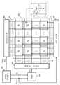
도 1은 본 발명의 한 실시예에 따른 터치 겸용 디스플레이 장치를 개략적으로 나타낸 블록도이다.
도 2는 본 발명의 한 실시예에 따른 패널의 구동 파형도이다.
도 3은 본 발명의 한 실시예에 따른 패널의 구동 타이밍도이다.
도 4는 본 발명의 한 실시예에 따른 PMIC를 경유하는 타이밍 컨트롤러와 게이트 구동부의 신호 연결 관계를 나타낸 도면이다.
도 5는 본 발명의 한 실시예에 따른 PMIC의 입출력 구동 파형도이다.
도 6은 본 발명의 한 실시예에 따른 PMIC의 입출력 구동 파형도이다.
도 7은 본 발명의 한 실시예에 따른 게이트 구동 회로의 일부를 나타낸 블록도이다.
도 8은 본 발명의 한 실시예에 따른 브릿지 GIP 스테이지를 중심으로 한 구동 파형도이다.
도 9는 본 발명의 한 실시예에 따른 EX_QB 신호 및 BCLK 신호를 생성하는 PMIC의 내부 구성을 나타낸 등가 회로도이다.1 is a block diagram schematically showing a touch-compatible display device according to an embodiment of the present invention.
2 is a driving waveform diagram of a panel according to an embodiment of the present invention.
3 is a driving timing diagram of a panel according to an embodiment of the present invention.
4 is a diagram illustrating a signal connection relationship between a timing controller and a gate driver via a PMIC according to an embodiment of the present invention.
5 is an input / output driving waveform diagram of a PMIC according to an embodiment of the present invention.
6 is an input / output driving waveform diagram of a PMIC according to an embodiment of the present invention.
7 is a block diagram showing a part of a gate driving circuit according to an embodiment of the present invention.
8 is a driving waveform diagram based on a bridge GIP stage according to an embodiment of the present invention.
9 is an equivalent circuit diagram illustrating an internal configuration of a PMIC for generating an EX_QB signal and a BCLK signal according to an embodiment of the present invention.
도 1은 본 발명의 한 실시예에 따른 터치 겸용 디스플레이 장치의 구성을 나타낸 블록도이고, 도 2는 본 발명의 한 실시예에 따른 패널의 구동 파형도이다.FIG. 1 is a block diagram showing the configuration of a touch-sensitive display device according to an embodiment of the present invention, and FIG. 2 is a driving waveform diagram of a panel according to an embodiment of the present invention.
도 1을 참조하면, 터치 겸용 디스플레이 장치는 타이밍 컨트롤러(100), PMIC(200), 게이트 구동부(300), 데이터 구동부(400), 패널(500), 터치 센싱부(600) 등을 구비한다.Referring to FIG. 1, the touch-sensitive display device includes a
타이밍 컨트롤러(100)는 호스트 시스템(도시 생략)으로부터 영상 데이터와, 타이밍 신호들을 공급받는다. 타이밍 신호들은 도트 클럭, 데이터 인에이블 신호, 수직 동기 신호, 수평 동기 신호를 포함한다. 수직 동기 신호 및 수평 동기 신호는 데이터 인에이블 신호를 카운트하여 생성할 수 있으므로 생략 가능하다.The
타이밍 컨트롤러(100)는 호스트 시스템으로부터 공급받은 영상 데이터(data)를 화질 보정 등과 같은 다양한 영상 처리를 수행하여 데이터 구동부(400)로 공급한다.The
타이밍 컨트롤러(100)는 호스트 시스템으로부터 공급받은 타이밍 신호들을 이용하여 데이터 구동부(400)의 동작 타이밍을 제어하는 데이터 제어 신호들(DCS)을 생성하여 데이터 구동부(400)로 공급한다. 예를 들면, 데이터 제어 신호들은(DCS)는 데이터의 래치 타이밍을 제어하는데 이용되는 소스 스타트 펄스, 소스 샘플링 클럭, 데이터의 출력 기간을 제어하는 소스 출력 인에이블 신호 등을 포함한다.The
타이밍 컨트롤러(100)는 호스트 시스템으로부터 공급받은 타이밍 신호들을 이용하여 게이트 구동부(300)의 구동 타이밍을 제어하는 게이트 제어 신호들을 생성하는데 이용되는 심플 타이밍 신호들(TC)를 생성하여 PMIC(200)로 공급한다. 예를 들면, 심플 타이밍 신호들(TC)는 제1 및 제2 초기 스타트 펄스(iVST1, iVST2; 도 5 참조), 온 클럭(ON_CLK; 도 5 참조), 오프 클럭(OFF_CLK; 도 5 참조), 제1 및 제2 초기 리셋 신호(iDRST, iBRST; 도 5 참조) 등을 포함한다.The
타이밍 컨트롤러(100)는 호스트 시스템으로부터 공급받은 타이밍 신호들을 이용하여 각 프레임 기간을 적어도 하나의 디스플레이 구동 기간(TD1~TDN)과 적어도 하나의 터치 센싱 기간(TS1~TSN)으로 시분할하기 위한 터치 동기 신호(Tsync)를 생성하여 PMIC(200) 및 터치 센싱부(600)로 공급한다.The
타이밍 컨트롤러(100)는 호스트 시스템으로부터 전송받은 영상 데이터를 내부 메모리에 저장하고, 각 디스플레이 구동 기간(TD)에서 메모리에 저장된 영상 데이터를 라이팅 속도보다 빠른 리딩 속도로 데이터 구동부(400)로 공급함과 아울러 게이트 구동부(300) 및 데이터 구동부(400)의 동작 타이밍을 제어하여 디스플레이 구동 기간(TD)에 패널(500)의 픽셀 어레이에 데이터 전압이 기입되게 한다. 타이밍 컨트롤러(100)는 터치 센싱 기간(TS)에 영상 데이터를 데이터 구동부(400)로 공급하지 않는다.The
PMIC(200)는 터치 겸용 디스플레이 장치에서 필요로 하는 다양한 구동 전압들을 생성하여 공급함과 아울러 타이밍 컨트롤러(100)로부터 공급받은 심플 타이밍 신호들(TC) 및 터치 동기 신호(Tsync)를 이용하여 게이트 구동부(300)를 제어하는 게이트 제어 신호들(GCS)을 생성하여 공급한다.The PMIC 200 generates and supplies various driving voltages required by the touch-compatible display device and supplies the generated driving voltages to the gate driver (not shown) using the simple timing signals TC and the touch synchronous signal Tsync received from the timing controller 100 (GCS) for controlling the gate control signal (GCS).
PMIC(200)는 외부로부터 공급받은 입력 전압을 이용하여 터치 겸용 디스플레이 장치의 모든 회로 구성, 즉 타이밍 컨트롤러(100), 게이트 구동부(300), 데이터 구동부(400), 패널(500), 터치 센싱부(600)의 구동에 필요한 각종 구동 전압들을 생성하여 출력한다. 예를 들면, PMIC(200)는 입력 전압을 이용하여 타이밍 컨트롤러(100) 및 데이터 구동부(400), 터치 센싱부(600) 등에 공급되는 디지털 구동 전압(VCC, GND)과, 패널(500)에 공급되는 공통 전압(Vcom), 데이터 구동부(400)에 공급되는 아날로그 구동 전압(VDD), 게이트 구동부(300)에 공급되는 게이트 온 전압(VGH) 및 게이트 오프 전압(VGL) 등을 생성하여 출력한다.The PMIC 200 receives the input voltage supplied from the outside and controls the entire circuit configuration of the touch-sensitive display device, that is, the
PMIC(200)는 타이밍 컨트롤러(100)로부터 공급받은 심플 타이밍 신호들(TC)과 터치 동기 신호(Tsync)를 이용하여 게이트 구동부(300)의 동작 타이밍을 제어하는 게이트 제어 신호들(GCS)을 생성하고 레벨 쉬프팅하여 게이트 구동부(300)로 공급한다.The PMIC 200 generates gate control signals GCS for controlling the operation timing of the
예를 들면, PMIC(200)는 타이밍 컨트롤러(100)로부터 공급받은 초기 스타트 펄스(iVST1, iVST2; 도 5 참조), 온 클럭(ON_CLK; 도 5 참조), 오프 클럭(OFF_CLK; 도 5 참조), 초기 리셋 신호(iDRST, iBRST; 도 5 참조) 등을 이용하여 게이트 구동부(300)에서 각 프레임마다 구동 시작을 지시하는 스타트 펄스(VST1, VST2; 도 5 참조), 각 디스플레이 구동 기간(TD)에서 스캔 출력으로 이용되는 다수의 쉬프트 클럭들(GCLK1~GCLK8; 도 5 참조), 게이트 구동부(300)의 초기화 신호로 이용되는 리셋 신호(BRST, DRST; 도 5 참조) 등을 생성하고, 생성된 게이트 제어 신호들(GCS)의 스윙폭이 증가하도록 레벨 쉬프팅하여 게이트 구동부(300)로 공급한다.5), an on-clock (ON_CLK; see FIG. 5), an off-clock (OFF_CLK; see FIG. 5), and an off-clock (OFF_CLK, see FIG. 5) supplied from the
특히, PMIC(200)는 타이밍 컨트롤러(100)로부터 공급받은 초기 리셋 신호(iBRST, iDRST; 도 6 참조)와 터치 동기 신호(Tsync; 도 6 참조)를 이용하여 각 터치 센싱 기간(TS)에서, 디스플레이 구동 기간(TD)과 다르게 게이트 구동부(300)를 제어하는 다른 게이트 제어 신호들(EX_QB, BCLK; 도 6 참조)을 생성하여 게이트 구동부(300)로 공급한다. 이에 대한 상세한 설명은 후술하기로 한다.In particular, in each touch sensing period (TS), the
데이터 구동부(400)는 타이밍 컨트롤러(100)로부터 공급된 데이터 제어 신호에 응답하여, 디스플레이 구동 기간(TD)에서 타이밍 컨트롤러(100)로부터 공급된 영상 데이터를 아날로그 신호로 변환하여 패널(500)의 데이터 라인들(DL)로 공급한다. 데이터 구동부(400)는 자신에게 내장되거나, 외부에 별도로 구비된 감마 전압 생성부(도시 생략)로부터 공급된 기준 감마 전압 세트를 데이터의 계조값에 각각 대응하는 계조 전압들로 세분화한다. 데이터 구동부(400)는 세분화된 계조 전압들을 이용하여 디스플레이 구동 기간(TD)에서 디지털 데이터를 정극성 또는 부극성 아날로그 데이터 전압(Vdata+, Vdata-)로 변환하고, 일정 단위로 전압 극성이 인버젼되는 데이터 전압(Vdata+, Vdata-)을 패널(500)의 데이터 라인들(DL)로 각각 공급한다.In response to the data control signal supplied from the
게이트 구동부(300)는 PMIC(200)로 공급된 게이트 제어 신호(GCS)에 응답하여, 각 디스플레이 구동 기간(TD)에서 패널(500)의 게이트 라인들(GL)을 순차 구동한다. 각 디스플레이 구동 기간(TD)에서 게이트 드라이버(420)는 해당 블록의 게이트 라인(GL)에 해당 스캔 기간마다 게이트 온 전압(VGH)의 스캔 펄스를 공급하고, 다른 게이트 라인(GL)이 구동되는 나머지 기간에는 게이트 오프 전압(VGH)을 공급한다. 각 터치 센싱 기간(TS)에서 게이트 구동부(300)는 스캔 펄스를 출력하지 않는다.The
이를 위하여, 게이트 구동부(300)은 게이트 라인들(GL)을 다수의 디스플레이 구동 기간(TD1~TDN)으로 각각 분할하여 구동하는 다수의 GIP 블록(#1~#N; 도 4 참조)과, 인접한 GIP 블록들 사이에 위치하여, 인접한 디스플레이 구동 기간들 사이의 터치 센싱 기간(TS)에서 GIP 회로의 시퀀셜 회로 특성을 유지시키는 브릿지 GIP 회로(BGIP1, BGIP2, ...)를 포함하며, GIP 블록들(#1~#N) 각각은 해당 블록의 다수의 게이트 라인들을 개별적으로 순차 구동하는 다수의 GIP 회로들을 포함한다. 또한, 게이트 구동부(300)은 GIP 회로의 안정적인 구동을 위한 더미 회로(도시 생략)를 더 구비한다.To this end, the
패널(500)은 터치 겸용 디스플레이 기능을 갖는 것으로, 픽셀들(P)이 매트릭스 형태로 배열된 픽셀 어레이를 통해 영상을 표시하고, 공통 전극 겸용 터치 전극(TE)을 이용하여 커패시턴스 방식으로 터치 여부를 센싱한다.The
패널(500)은 유기 발광 다이오드 디스플레이 패널 또는 액정 디스플레이 패널일 수 있으며, 본 발명의 실시예에서는 액정 디스플레이 패널을 예를 들어 설명한다. 커패시턴스 터치 방식은 상호 커패시턴스(Mutual Capacitance) 터치 방식과, 셀프 커패시턴스(Self-Capacitance) 터치 방식 중 어느 하나를 이용할 수 있으며, 본 발명의 실시예에서는 셀프 커패시턴스 터치 방식을 예로 들어 설명한다.The
패널(500)의 픽셀들(P) 각각은 게이트 라인(GL) 및 데이터 라인(DL)과 접속된 박막 트랜지스터(TFT)와, 박막 트랜지스터(TFT)와 접속된 액정 커패시터(Clc) 및 스토리지 커패시터(Cst)를 구비한다. 액정 커패시터(Clc)는 박막 트랜지스터(TFT)를 통해 화소 전극에 공급된 데이터 신호와, 공통 전극 겸용 터치 전극(TE)에 공급된 공통 전압과의 차전압을 충전하고 충전된 전압에 따라 액정을 구동하여 광투과율을 조절한다. 스토리지 커패시터(Cst)는 액정 커패시터(Clc)에 충전된 전압을 안정적으로 유지시킨다.Each of the pixels P of the
패널(500)은 픽셀 어레이에 포함되는 다수의 터치 전극열을 포함하고, 다수의 터치 전극열 각각은 데이터 라인(DL)의 길이 방향으로 배열된 다수의 터치 전극(TE)과, 다수의 터치 전극(TE)과 개별적으로 접속되고 터치 센싱부(600)와 접속된 다수의 신호 라인(TL)을 포함한다. 다수의 터치 전극들(TE)은 픽셀 어레이에 형성된 공통 전극이 분할되어 형성된 것으로, 각 터치 전극(TE)은 터치점 크기를 고려하여 다수의 픽셀을 포함하는 일정 크기로 형성된다.The
터치 센싱부(600)는 타이밍 컨트롤러(100)로부터 공급된 터치 동기 신호(Tsync)에 응답하여, 터치 센싱 기간(TS)에서 신호 라인들(TL)을 통해 터치 전극(TE)에 터치 구동 신호(Vtouch)를 공급한 다음, 해당 터치 전극(TE)으로부터의 피드백 신호를 수신한다. 터치 센싱부(600)는 각 터치 전극(TE)에 대한 터치 구동 신호(Vtouch)와 피드백 신호를 차동 증폭하여 터치로 인한 각 터치 전극(TE)의 셀프 커패시턴스 변화(신호 지연량)를 센싱하여 센싱 정보를 생성하고, 센싱 정보를 신호 처리하여 터치 좌표 정보를 산출하고, 터치 좌표 정보를 호스트 시스템(100)으로 출력한다.The
터치 센싱부(600)는 터치 IC로 집적화되거나, 데이터 구동부(400)와 함께 구동 IC로 집적화되거나, 데이터 구동부(400) 및 타이밍 제어부(300)와 함께 구동 IC로 집적화될 수 있다. 데이터 구동부(400)는 적어도 하나의 IC로 구성되어 패널(500)과 연결될 수 있다.The
게이트 구동부(300)는 GIP(Gate In Panel) 방식으로 패널(500)의 박막 트랜지스터 어레이와 함께 형성되어 비표시 영역에 내장된다.The
도 2를 참조하면, 터치 동기 신호(Tsync)가 지시하는 제1 디스플레이 구동 기간(TD1)에서 게이트 구동부(300)는 제1 GIP 블록(#1; 도 3)의 게이트 라인들(GL11~G1i)을 순차 구동하고, 데이터 구동부(400)는 데이터 라인들(DL)로 데이터 전압(Vdata+, Vdata-)을 공급하며, 터치 센싱부(600)는 전원부로부터의 공통 전압(Vcom)을 신호 라인들(TL)을 통해 터치 전극들(TE)로 공급함으로써, 제1 블록의 픽셀들에 데이터 전압(Vdata+, Vdata-)을 기입한다.2, in the first display driving period TD1 indicated by the touch synchronizing signal Tsync, the
터치 동기 신호(Tsync)가 지시하는 제1 터치 센싱 기간(TS1)에서 터치 센싱부(600)는 신호 라인들(TL)을 통해 터치 전극들(TE) 각각에 터치 구동 신호(Vtouch)를 공급하고, 해당 터치 전극들(TE)로부터의 피드백 신호를 신호 라인들(TL)을 통해 입력하여 터치 여부를 센싱한다.In the first touch sensing period TS1 indicated by the touch synchronizing signal Tsync, the
그 다음, 제2 디스플레이 구동 기간(TD2)에서 게이트 구동부(300) 중 제2 GIP 블록(#2)의 게이트 라인들(GL21~GL2i)이 순차 구동되면서 전술한 바와 같이 제2 블록의 픽셀들에 데이터 전압(Vdata+, Vdata-)이 기입되고, 이어서 터치 센싱 기간(TS2)에서 전술한 바와 같이 터치 전극들(TE)을 구동하여 터치 여부를 센싱한다..Next, in the second display drive period TD2, the gate lines GL21 to GL2i of the second
이러한 디스플레이 구동 기간(TD)과 터치 센싱 기간(TS)은 교번적으로 반복되어, 제N GIP 블록(#N)의 게이트 라인들(GLN1~GLNi)이 순차 구동되면서 제N 블록의 픽셀들에 데이터 전압(Vdata+, Vdata-)이 기입되고, 이어서 터치 센싱 기간(TSN)에서 전술한 바와 같이 터치 전극들(TE)을 구동하여 터치 여부를 센싱한다The display driving period TD and the touch sensing period TS are alternately repeated so that the gate lines GLN1 to GLNi of the Nth GIP block #N are sequentially driven, Voltages Vdata + and Vdata- are written, and then, in the touch sensing period TSN, the touch electrodes TE are sensed by driving the touch electrodes TE as described above
한편, 도 3에 도시된 바와 같이, 각 터치 센싱 기간(TS)에서 터치 센싱부(600)는 게이트 구동부(300) 및 데이터 구동부(400)를 통해 게이트 라인들(GL) 및 데이터 라인들(DL)에도 터치 구동 신호(Vtouch)를 공급하여 로드 프리 구동(Load Free Driving)을 함으로써 터치 전극(TE) 및 신호 라인(TL)의 RC 로드(Resistor Capacitor Load)를 최소화하여 터치 센싱 감도를 향상시킬 수 있다.3, in each touch sensing period TS, the
이를 위하여, 게이트 구동부(300)의 출력단과 데이터 구동부(400)의 출력단에는 각각 출력 선택부(도시 생략)를 추가로 구비할 수 있다. 게이트 구동부(300)의 출력단에 구비되는 출력 선택부는 터치 구동 신호(Vtouch)에 응답하여 디스플레이 구동 기간(TD)에서는 게이트 구동부(300)로부터 공급된 스캔 신호를 선택하여 출력하고, 터치 센싱 기간(TS)에서는 터치 센싱부(600)로부터 공급된 터치 구동 신호(Vtouch)를 선택하여 출력할 수 있다. 데이터 구동부(400)의 출력단에 구비되는 출력 선택부는 터치 동기 신호(Tsync)에 응답하여, 디스플레이 구동 기간(TD)에서는 데이터 구동부(400)로부터 공급된 데이터 신호를 선택하여 출력하고, 터치 센싱 기간(TS)에서는 터치 센싱부(600)로부터 공급된 터치 구동 신호(Vtouch)를 선택하여 출력할 수 있다.For this, an output selection unit (not shown) may be additionally provided at the output terminal of the
도 4는 본 발명의 한 실시예에 따른 PMIC(200)를 경유하는 타이밍 컨트롤러(100)와 게이트 구동부(300)의 신호 연결 관계를 나타낸 도면이고, 도 5 및 도 6은 본 발명의 한 실시예에 따른 PMIC의 입출력 구동 파형도이다.4 and 5. FIG. 4 is a diagram illustrating a signal connection relationship between the
도 4를 참조하면, 타이밍 컨트롤러(100)는 도 5에 도시된 바와 같이 2개의 초기 스타트 펄스(iVST1, iVST2), 온 클럭(ON_CLK), 오프 클럭(OFF_CLK), 2개의 초기 리셋 신호(iDRST, iBRST)를 포함하는 총 6개의 심플 타이밍 신호들(TC)을 각 전송 라인을 통해 PMIC(200)로 공급하고, 터치 동기 신호(Tsync)를 터치 센싱부(600) 및 PMIC(200)로 공급한다. 즉, PMIC(200)는 타이밍 컨트롤러(100)로부터 터치 센싱부(600)로 터치 동기 신호(Tsync)를 공급하는 전송 라인을 공유한다.4, the
PMIC(200)는 타이밍 컨트롤러(100)로부터 공급받은 6개의 심플 타이밍 신호들(TC)과 터치 동기 신호(Tsync)를 이용하여 스타트 펄스(VST1, VST2), 다수의 쉬프트 클럭들, 예를 들면 8개의 쉬프트 클럭들(CLK1~CLK8), 리셋 신호(DRST, BRST), 브릿지 클럭(BCLK), QB 외부 제어 신호(EX_QB)를 포함하는 총 14개의 게이트 제어 신호(GCS)를 생성하고, 14개의 게이트 제어 신호(GCS)를 각 전송 라인을 통해 게이트 구동부(300)로 공급한다.The
스타트 펄스(VST1, VST2)는 각 프레임마다 디스플레이 구동 기간(TD1)에서 게이트 구동부(300)의 동작 시작을 지시하는 역할을 한다. PMIC(200)는 타이밍 컨트롤러(100)로부터 공급된 초기 스타트 펄스(iVST1, iVST2)를 레벨 쉬프팅하여 스타트 펄스(VST1, VST2)로써 게이트 구동부(300)로 공급한다. 하이 구간이 서로 오버랩하지 않도록 위상차를 갖는 2개의 스타트 펄스(VST1, VST2)는 패널(500)의 양측에서 게이트 라인들을 교번적으로 구동하는 제1 및 제2 게이트 구동부(도시 생략)에 각각 공급되는 것이며, 게이트 구동부(300)가 분할되지 않으면 하나의 스타트 펄스만(VST)만 게이트 구동부(300)로 공급될 수 있다.The start pulses VST1 and VST2 serve to instruct the start of the operation of the
PMIC(200)는 온 클럭(ON_CLK), 오프 클럭(OFF_CLK)을 이용하여 각 디스플레이 구동 기간(TD)에서 쉬프트 클럭들(CLK1~CLK8)을 생성 및 레벨 쉬프팅하여 게이트 구동부(300)로 공급한다. PMIC(200)으로부터 게이트 구동부(300)로 공급되는 쉬프트 클럭들(GCLK1~GCLK8)은 온 클럭(ON_CLK)의 라이징 타임에 응답하여 순차적으로 라이징되고, 오프 클럭(OFF_CLK)의 폴링 타임에 응답하여 순차적으로 폴링되며, 인접한 쉬프트 클럭과 일부 구간이 서로 중첩되는 형태를 갖는다. 게이트 구동부(300)에서 GIP 블록들(#1, #2, ..., #N) 각각은 쉬프트 클럭들(GCLK1~GCLK8)을 순차적으로 번갈아가면서 선택하여 순차적으로 위상 쉬프트되는 스캔 출력(GL11~ GL1i, GL21~ GL2i, ..., GLN11~ GLNi)으로 출력한다.The
리셋 신호(DRST, BRST)는 수직 동기 신호의 블랭크(Blank) 기간에서 게이트 구동부(300)에 포함된 더미 회로 및 GIP 회로를 초기화하기 위하여 공급된다. 리셋 신호(DRST)의 펄스는 스타트 펄스(VST1) 이전의 블랭크(Blank) 기간에 게이트 구동부(300)의 더미 회로에 공급되어, 안정적인 초기 구동을 위해 유효 GIP 회로 이전에 더미 회로의 구동을 지시하는 역할을 한다. 리셋 신호(BRST)의 펄스는 블랭크 기간에서 리셋 신호(DRST)의 펄스 이전에 공급되어 적어도 하나의 유효 GIP 회로를 초기화하는 역할을 한다. PMIC(200)는 타이밍 컨트롤러(100)로부터 공급된 초기 리셋 신호(iDRST, iBRST)를 레벨 쉬프팅하여 리셋 신호(DRST, BRST)로써 게이트 구동부(300)로 공급한다.The reset signals DRST and BRST are supplied to initialize the dummy circuit and the GIP circuit included in the
이를 위하여, 제1 초기 리셋 신호(iDRST)는 블랭크 기간에서 제1 리셋 신호(DRST)의 펄스로 이용되는 제1 펄스(P11)를 포함한다. 제2 초기 리셋 신호(iBRST)는 블랭크 기간에서 제2 리셋 신호(BRST)의 펄스로 이용되는 제1 펄스(P21)를 포함한다.To this end, the first initial reset signal iDRST includes a first pulse P11 used as a pulse of the first reset signal DRST in the blank period. The second initial reset signal iBRST includes a first pulse P21 used as a pulse of the second reset signal BRST in the blank period.
그리고, 도 6에 도시된 바와 같이, 초기 리셋 신호(iDRST, iBRST)는 각 디스플레이 구동 기간(TD)에 공급되는 제2 펄스(P11, P21)와, 각 터치 센싱 기간(TS)에 공급되는 제3 펄스(P13, P23)를 더 포함한다.6, the initial reset signals iDRST and iBRST are supplied with the second pulses P11 and P21 supplied during each display driving period TD and the second pulses P11 and P21 supplied during the respective touch sensing periods TS 3 pulses P13 and P23.
PMIC(200)는 각 디스플레이 구동 기간(TD)에서 초기 리셋 신호(iDRST, iBRST)의 제2 펄스(P11, P21)와, 터치 동기 신호(Tsync)를 논리 조합하여 QB 외부 제어 신호(EX_QB)를 생성 및 레벨 쉬프팅하여 게이트 구동부(300)로 공급한다.The
PMIC(200)는 각 터치 센싱 기간(TD)에서 초기 리셋 신호(iDRST, iBRST)의 제3 펄스(P11, P21)와, 터치 동기 신호(Tsync)를 논리 조합하여 브릿지 클럭(BCLK)을 생성 및 레벨 쉬프팅하여 게이트 구동부(300)로 공급한다.The
도 7을 참조하면, QB 외부 제어 신호(EX_QB) 및 브릿지 클럭(BCLK)은 게이트 구동부(300)에서 인접한 GIP 블록들(#1, #2) 사이에 배치된 브릿지 GIP 회로(BGIP1)에 공급된다. 브릿지 GIP 회로(BGIP1)는 터치 센싱 기간(TS)에서 인접한 GIP 블록들(#1, #2) 사이에 시퀀셜 회로 특성을 유지하는 역할을 한다.7, the QB external control signal EX_QB and the bridge clock BCLK are supplied to the bridge GIP circuit BGIP1 disposed between the adjacent
도 8을 참조하면, 브릿지 클럭(BCLK)은 터치 센싱 기간(TS1)에서 주기적으로 반복하여 브릿지 GIP 회로(BGIP1)에 공급되어, 이전 GIP 블록으로부터 공급된 하이 상태의 스캔 출력에 의해 하이 상태로 충전된 브릿지 GIP 회로(BGIP1)의 Q 노드의 방전을 방지하면서 하이 상태를 유지시키는 역할을 한다. 이에 따라, 다음 GIP 블록과 연결된 브릿지 GIP 회로(BGIP1)의 출력이 터치 센싱 기간(TS1)에서 하이 상태(액티브 상태)를 유지하여, 다음 디스플레이 구동 기간(TD2)에서 다음 GIP 블록(#2)의 첫번째 GIP 회로의 스타트 펄스로 공급됨으로써 다음 GIP 블록(#2)은 클럭들(CLK1~CLK8)을 이용하여 순차적인 스캔 펄스를 출력할 수 있다.Referring to FIG. 8, the bridge clock BCLK is periodically and repeatedly supplied to the bridge GIP circuit BGIP1 in the touch sensing period TS1 so as to be charged to a high state by a scan output of a high state supplied from a previous GIP block. And prevents the Q node of the bridge GIP circuit (BGIP1) from discharging and maintains the high state. Thus, the output of the bridge GIP circuit BGIP1 connected to the next GIP block maintains the high state (active state) in the touch sensing period TS1, and the output of the next
QB 외부 제어 신호(EX_QB)는 각 디스플레이 구동 기간(TD)의 초반부에서 브릿지 GIP 회로(BGIP)에 공급되어 QB 노드의 제어를 통해 다음 GIP 블록과 연결된 브릿지 GIP 출력을 로우 상태로 방전시키는 역할을 함으로써 브릿지 GIP 회로(BGIP)에 의해 GIP 블록의 신뢰성 문제가 야기되는 것을 방지한다.The QB external control signal EX_QB is supplied to the bridge GIP circuit BGIP in the first half of each display driving period TD and discharges the bridge GIP output connected to the next GIP block to the low state through the control of the QB node Thereby preventing the reliability problem of the GIP block from being caused by the bridge GIP circuit (BGIP).
브릿지 GIP 회로를 포함하는 각 GIP 회로는 일반적으로 Q 노드에 의해 제어되어 입력 클럭을 출력 신호로 공급하는 풀-업 트랜지스터(도시 생략)과, 저전위 구동 전원(VSS)을 출력 신호로 공급하는 풀-다운 트랜지스터(도시 생략)를 구비한다.Each GIP circuit including a bridge GIP circuit generally includes a pull-up transistor (not shown) that is controlled by a Q node to supply an input clock to an output signal, a pull-up transistor - down transistors (not shown).
브릿지 클럭(BCLK)은 브릿지 GIP 회로의 풀-업 트랜지스터에 공급되어 출력 신호로 이용됨과 아울러 Q 노드의 전위를 상승시키는 역할을 하게 되고, QB 외부 제어 신호(EX_QB)는 풀-다운 트랜지스터의 제어 노드에 공급된다.The bridge clock BCLK is supplied to the pull-up transistor of the bridge GIP circuit to be used as an output signal and to raise the potential of the Q node. The QB external control signal EX_QB is supplied to the control node .
도 9는 본 발명의 한 실시예에 따른 PMIC(300)에서 브릿지 클럭(BCLK) 및 QB 외부 제어 신호(EX_QB)를 생성하는 회로 블록을 나타낸 등가 회로도이다.9 is an equivalent circuit diagram showing a circuit block for generating a bridge clock BCLK and a QB external control signal EX_QB in the
도 9를 참조하면, PMIC(300)는 타이밍 컨트롤러(100)로부터 공급받은 터치 동기 신호(Tsync)와 제1 및 제2 초기 리셋 신호(iDRST, iBRST)를 논리곱 연산하여 레벨 쉬프터(LS)를 통해 QB 외부 제어 신호(EX_QB)를 출력하는 제1 앤드 게이트(AND1)를 구비한다.9, the
PMIC(300)는 타이밍 컨트롤러(100)로부터 공급받은 터치 동기 신호(Tsync)를 논리 반전시키고, 논리 반전된 터치 동기 신호(Tsync)와 제1 및 제2 초기 리셋 신호(iDRST, iBRST)를 논리곱 연산하여 레벨 쉬프터(LS)를 통해 브릿지 클럭(BCLK)을 출력하는 제2 앤드 게이트(AND2)를 구비한다.The
제1 앤드 게이트(AND1)는 각 디스플레이 구동 기간(TD)에서 초기 리셋 신호(iDRST, iBRST)의 제2 펄스(P11, P21)와, 하이 상태의 터치 동기 신호(Tsync)를 논리곱 연산함으로써 QB 외부 제어 신호(EX_QB)의 하이 펄스를 레벨 쉬프터(LS)를 통해 게이트 구동부(300)의 브릿지 GIP 회로 공급하고, 나머지 기간에서는 QB 외부 제어 신호(EX_QB)의 로우 논리를 출력한다.The first AND gate AND1 ANDs the second pulse P11 and P21 of the initial reset signals iDRST and iBRST in the respective display driving periods TD and the high- The high pulse of the external control signal EX_QB is supplied to the bridge GIP circuit of the
제1 앤드 게이트(AND1)는 각 터치 센싱 기간(TS)에서 초기 리셋 신호(iDRST, iBRST)의 제3 펄스(P13, P23)와, 하이 상태로 논리 반전된 터치 동기 신호(Tsync)를 논리곱 연산함으로써 브릿지 클럭(BCLK)을 레벨 쉬프터(LS)를 통해 게이트 구동부(300)의 브릿지 GIP 회로 공급하고, 나머지 기간에서는 브릿지 클럭(BCLK)의 로우 논리를 출력한다.The first AND gate AND1 ANDs the third pulse P13 and P23 of the initial reset signals iDRST and iBRST and the touch synchronous signal Tsync logically inverted in the high state in each touch sensing period TS Thereby supplying the bridge clock BCLK to the bridge GIP circuit of the
전술한 바와 같이, 본 발명의 한 실시예에 따른 터치 겸용 디스플레이 장치용 구동 회로는 타이밍 컨트롤러(100)로부터 터치 센싱부(600)로 공급되는 터치 동기 신호(Tsync)와 타이밍 컨트롤러(100)로부터 PMIC(200)로 공급되는 기존의 심플 타이밍 신호들(TC)을 이용하여 디스플레이 구동 기간과 터치 센싱 기간에 서로 다른 게이트 제어 신호들(GCS)을 생성하여 게이트 구동부(300)로 공급할 수 있다.The driving circuit for a touch-sensitive display device according to an embodiment of the present invention includes a touch synchronizing signal Tsync supplied from the
따라서, 본 발명의 한 실시예에 따른 터치 겸용 디스플레이 장치용 구동 회로는 타이밍 컨트롤러(100)의 출력핀 수와, 인쇄 회로 기판의 신호 라인의 수 및 라우팅 면적이 증가되지 않아도 되므로 코스트 상승을 방지할 수 있다.Therefore, since the number of output pins of the
이상의 설명은 본 발명을 예시적으로 설명한 것에 불과하며, 본 발명이 속하는 기술 분야에서 통상의 지식을 가진 자에 의해 본 발명의 기술적 사상에서 벗어나지 않는 범위에서 다양한 변형이 가능할 것이다. 따라서 본 발명의 명세서에 개시된 실시예들은 본 발명을 한정하는 것이 아니다. 본 발명의 범위는 아래의 특허청구범위에 의해 해석되어야 하며, 그와 균등한 범위 내에 있는 모든 기술도 본 발명의 범위에 포함되는 것으로 해석되어야 한다.The foregoing description is merely illustrative of the present invention, and various modifications may be made by those skilled in the art without departing from the spirit of the present invention. Accordingly, the embodiments disclosed in the specification of the present invention are not intended to limit the present invention. It is intended that the scope of the invention be interpreted by the claims appended hereto, and that all techniques within the scope of equivalents thereof should be construed as being included within the scope of the present invention.
100: 타이밍 컨트롤러 200: 전원 관리 IC
300: 게이트 구동부 400: 데이터 구동부
500: 패널 600: 터치 센싱부
210, 220: 앤드 게이트 230: 레벨 쉬프터
DL: 데이터 라인 GL: 게이트 라인
TE: 공통 전극 겸용 터치 전극 TL: 신호 라인
P: 픽셀 AND1, AND2: 앤드 게이트
LS: 레벨 쉬프터100: timing controller 200: power management IC
300: Gate driver 400: Data driver
500: Panel 600: Touch sensing unit
210, 220: AND gate 230: level shifter
DL: Data line GL: Gate line
TE: Common electrode common touch electrode TL: Signal line
P: pixel AND1, AND2: AND gate
LS: level shifter
Claims (5)
Translated fromKorean제1 및 제2 초기 리셋 신호와, 터치 동기 신호를 생성하여 출력하는 타이밍 컨트롤러와,
상기 타이밍 컨트롤러부터 공급된 상기 터치 동기 신호와 상기 제1 및 제2 초기 리셋 신호를 논리 연산하여 상기 브릿지 GIP 회로의 Q 노드와 QB 노드를 각각 제어하는 브릿지 클럭과, QB 외부 제어 신호를 생성하여 상기 게이트 구동부로 출력하는 전원 관리 회로를 구비하는 터치 겸용 디스플레이 장치용 구동 회로.A plurality of GIP blocks for dividing the gate lines of the touch-panel display panel into a plurality of blocks to drive a plurality of blocks in a plurality of display driving periods, and a bridge GIP A gate driver including a circuit;
A timing controller for generating and outputting first and second initial reset signals and a touch synchronous signal,
A bridge clock for controlling the Q node and the QB node of the bridge GIP circuit by logically operating the touch synchronous signal supplied from the timing controller and the first and second initial reset signals, And a power management circuit for outputting the signal to the gate driver.
상기 터치 동기 신호는 각 프레임 기간을 상기 다수의 디스플레이 구동 기간과, 상기 다수의 디스플레이 구동 기간 중 인접한 디스플레이 구동 기간들 사이에 할당된 각 터치 센싱 기간을 지시하고,
상기 제1 및 제2 초기 리셋 신호는 상기 각 프레임의 블랭크 기간에 서로 오버랩없이 공급되는 제1 펄스와, 상기 각 디스플레이 구동 기간에 동시 공급되는 제2 펄스와, 상기 각 터치 센싱 기간에 주기적으로 동시 공급되는 제3 펄스를 포함하는 터치 겸용 디스플레이 장치용 구동 회로.The method according to claim 1,
Wherein the touch synchronization signal indicates each touch sensing period allocated between adjacent display driving periods of the plurality of display driving periods and each of the plurality of display driving periods,
Wherein the first and second initial reset signals include a first pulse supplied in a blank period of each frame without overlapping with each other, a second pulse simultaneously supplied in each display driving period, And a third pulse to be supplied to the driving circuit.
상기 전원 관리 회로는
상기 터치 동기 신호와 상기 제1 및 제2 초기 리셋 신호를 논리곱 연산하여 출력하는 제1 앤드 게이트와,
상기 터치 동기 신호를 논리 반전시키고, 논리 반전된 터치 동기 신호와 상기 제1 및 제2 초기 리셋 신호를 논리곱 연산하여 출력하는 제2 앤드 게이트와,
상기 제1 앤드 게이트의 출력을 레벨 쉬프팅하여 상기 QB 외부 제어 신호로 출력하고, 상기 제2 앤드 게이트의 출력을 레벨 쉬프팅하여 상기 브릿지 클럭으로 공급하는 레벨 쉬프터를 구비하는 터치 겸용 디스플레이 장치용 구동 회로.The method of claim 2,
The power management circuit
A first AND gate for performing an AND operation of the touch synchronous signal and the first and second initial reset signals,
A second AND gate for logically inverting the touch synchronous signal, performing a logical AND operation on the first and second initial reset signals and the logic inverted touch synchronous signal,
And a level shifter for level-shifting the output of the first AND gate to output the QB external control signal and level-shifting the output of the second AND gate to supply the bridge clock signal.
상기 브릿지 회로는
상기 각 터치 센싱 기간에서 상기 브릿지 클럭을 이용하여 이전 GIP 블록으로부터 공급된 스캔 출력의 액티브 상태를, 해당 터치 센싱 기간동안 유지하여, 그 다음 디스플레이 구동 기간에서 다음 GIP 블록의 스타트 펄스로 공급하고,
상기 각 디스플레이 구동 기간에서 상기 QB 외부 제어 신호를 이용하여 상기 브릿지 GIP 회로의 출력을 방전시키는 터치 겸용 디스플레이 장치용 구동 회로.The method of claim 2,
The bridge circuit
The active state of the scan output supplied from the previous GIP block is maintained for the corresponding touch sensing period using the bridge clock in each of the touch sensing periods and is supplied as the start pulse of the next GIP block in the next display driving period,
And the output of the bridge GIP circuit is discharged using the QB external control signal in each of the display driving periods.
상기 타이밍 컨트롤러는 상기 각 프레임을 시작을 지시하는 초기 스타트 펄스와, 상기 각 디스플레이 구동 기간에서만 온 클럭, 오프 클럭을 더 생성하여 상기 전원 관리 회로로 공급하고,
상기 전원 관리 회로는 상기 초기 스타트 펄스를 레벨 쉬프팅하여 스타트 펄스를 상기 게이트 구동부로 공급하고, 상기 각 디스플레이 구동 기간에서 상기 온 클럭 및 오프 클럭을 이용하여 위상 쉬프트되는 다수의 클럭들을 생성 및 레벨 쉬프팅하여 상기 게이트 구동부로 공급하고, 상기 제1 및 제2 초기 리셋 신호의 상기 제1 펄스를 이용하여 상기 블랭크 기간에서 제1 및 제2 리셋 신호를 상기 게이트 구동부로 공급하는 터치 겸용 디스플레이 장치용 구동 회로.The method of claim 2,
Wherein the timing controller further generates an initial start pulse for indicating the start of each frame and an on clock and an off clock for each display driving period and supplies the on clock and the off clock to the power management circuit,
The power management circuit level-shifts the initial start pulse to supply a start pulse to the gate driver, generates and shifts a plurality of clocks phase-shifted using the on clock and the off clock in each display driving period And supplies the first and second reset signals to the gate driver using the first pulse of the first and second initial reset signals in the blank period.
Priority Applications (1)
| Application Number | Priority Date | Filing Date | Title |
|---|---|---|---|
| KR1020150174827AKR20170068073A (en) | 2015-12-09 | 2015-12-09 | Driving circuit for display device with touch |
Applications Claiming Priority (1)
| Application Number | Priority Date | Filing Date | Title |
|---|---|---|---|
| KR1020150174827AKR20170068073A (en) | 2015-12-09 | 2015-12-09 | Driving circuit for display device with touch |
Publications (1)
| Publication Number | Publication Date |
|---|---|
| KR20170068073Atrue KR20170068073A (en) | 2017-06-19 |
Family
ID=59278940
Family Applications (1)
| Application Number | Title | Priority Date | Filing Date |
|---|---|---|---|
| KR1020150174827AWithdrawnKR20170068073A (en) | 2015-12-09 | 2015-12-09 | Driving circuit for display device with touch |
Country Status (1)
| Country | Link |
|---|---|
| KR (1) | KR20170068073A (en) |
Cited By (7)
| Publication number | Priority date | Publication date | Assignee | Title |
|---|---|---|---|---|
| KR20190045518A (en)* | 2017-10-24 | 2019-05-03 | 엘지디스플레이 주식회사 | Touch sensing driving circuit |
| KR20190076219A (en)* | 2017-12-22 | 2019-07-02 | 엘지디스플레이 주식회사 | Display device |
| KR20200141874A (en)* | 2019-06-11 | 2020-12-21 | 엘지디스플레이 주식회사 | Driving circuit, touch display device, and driving method thereof |
| EP3855421A1 (en)* | 2020-01-17 | 2021-07-28 | Samsung Display Co., Ltd. | Clock generator and display device including the same |
| US11470500B2 (en)* | 2018-05-22 | 2022-10-11 | Telefonaktiebolagget LM Ericsson (Publ) | Short buffer status reports for multiple logical channel groups |
| US12057076B2 (en)* | 2022-06-27 | 2024-08-06 | Samsung Display Co., Ltd. | Display device including level shifter generating gate clock signals synchronized with rising edge and falling edge of clock signal |
| US20250259601A1 (en)* | 2024-02-13 | 2025-08-14 | Lg Display Co., Ltd. | Level shifter, display device including same, and method of driving display device |
- 2015
- 2015-12-09KRKR1020150174827Apatent/KR20170068073A/ennot_activeWithdrawn
Cited By (11)
| Publication number | Priority date | Publication date | Assignee | Title |
|---|---|---|---|---|
| KR20190045518A (en)* | 2017-10-24 | 2019-05-03 | 엘지디스플레이 주식회사 | Touch sensing driving circuit |
| KR20190076219A (en)* | 2017-12-22 | 2019-07-02 | 엘지디스플레이 주식회사 | Display device |
| US11470500B2 (en)* | 2018-05-22 | 2022-10-11 | Telefonaktiebolagget LM Ericsson (Publ) | Short buffer status reports for multiple logical channel groups |
| KR20200141874A (en)* | 2019-06-11 | 2020-12-21 | 엘지디스플레이 주식회사 | Driving circuit, touch display device, and driving method thereof |
| US11914810B2 (en) | 2019-06-11 | 2024-02-27 | Lg Display Co., Ltd. | Driving circuit, touch display device and driving method thereof |
| EP3855421A1 (en)* | 2020-01-17 | 2021-07-28 | Samsung Display Co., Ltd. | Clock generator and display device including the same |
| CN113223447A (en)* | 2020-01-17 | 2021-08-06 | 三星显示有限公司 | Clock generator and display device including the same |
| US11562696B2 (en) | 2020-01-17 | 2023-01-24 | Samsung Display Co., Ltd. | Clock generator and display device including the same |
| US12080245B2 (en) | 2020-01-17 | 2024-09-03 | Samsung Display Co., Ltd. | Clock generator and display device including the same |
| US12057076B2 (en)* | 2022-06-27 | 2024-08-06 | Samsung Display Co., Ltd. | Display device including level shifter generating gate clock signals synchronized with rising edge and falling edge of clock signal |
| US20250259601A1 (en)* | 2024-02-13 | 2025-08-14 | Lg Display Co., Ltd. | Level shifter, display device including same, and method of driving display device |
Similar Documents
| Publication | Publication Date | Title |
|---|---|---|
| CN107783688B (en) | Touch display device and method of driving the same | |
| US10656743B2 (en) | Display apparatus | |
| US10216319B2 (en) | Display device having touch sensor | |
| US10691242B2 (en) | Touch display device | |
| KR20170068073A (en) | Driving circuit for display device with touch | |
| CN103514847B (en) | Liquid crystal indicator and driving method thereof | |
| US9442593B2 (en) | Touch screen panel integrated display device and display panel | |
| KR102729883B1 (en) | Operational amplifier and touch display device using the same | |
| US10884556B2 (en) | Gate driving integrated circuit for a touch display and operating method thereof | |
| KR20140075543A (en) | Display device with integrated touch screen and method for driving the same | |
| KR102465444B1 (en) | Display with touch system | |
| US11693518B2 (en) | Touch driver circuitand driving method, and driver apparatus of touch display device | |
| KR20160094835A (en) | Display device, and driving device and method thereof | |
| TW202225933A (en) | Touch display device, method of driving thereof and timing controller | |
| KR102391616B1 (en) | Gate driver and touch screen integrated display device including the same | |
| KR20160081649A (en) | Gata driver and touch screen integrated display device including thereof | |
| KR102384762B1 (en) | Touch sensing driving circuit | |
| KR20140131448A (en) | Scan Driver and Display Device Using the same | |
| KR20170077639A (en) | Display device with touch | |
| KR102419441B1 (en) | Display panel with integrated touch electrodes and display apparatus using the same | |
| KR101580179B1 (en) | Display Apparatus | |
| KR20190047304A (en) | Display apparatus | |
| CN119252190A (en) | Display panel and display device |
Legal Events
| Date | Code | Title | Description |
|---|---|---|---|
| PA0109 | Patent application | Patent event code:PA01091R01D Comment text:Patent Application Patent event date:20151209 | |
| PG1501 | Laying open of application | ||
| PC1203 | Withdrawal of no request for examination |