KR20170061221A - Memory system and operating method of memory system - Google Patents
Memory system and operating method of memory systemDownload PDFInfo
- Publication number
- KR20170061221A KR20170061221AKR1020150165483AKR20150165483AKR20170061221AKR 20170061221 AKR20170061221 AKR 20170061221AKR 1020150165483 AKR1020150165483 AKR 1020150165483AKR 20150165483 AKR20150165483 AKR 20150165483AKR 20170061221 AKR20170061221 AKR 20170061221A
- Authority
- KR
- South Korea
- Prior art keywords
- memory
- segments
- data
- memory block
- super
- Prior art date
- Legal status (The legal status is an assumption and is not a legal conclusion. Google has not performed a legal analysis and makes no representation as to the accuracy of the status listed.)
- Withdrawn
Links
Images


Classifications
- G—PHYSICS
- G06—COMPUTING OR CALCULATING; COUNTING
- G06F—ELECTRIC DIGITAL DATA PROCESSING
- G06F3/00—Input arrangements for transferring data to be processed into a form capable of being handled by the computer; Output arrangements for transferring data from processing unit to output unit, e.g. interface arrangements
- G06F3/06—Digital input from, or digital output to, record carriers, e.g. RAID, emulated record carriers or networked record carriers
- G06F3/0601—Interfaces specially adapted for storage systems
- G06F3/0602—Interfaces specially adapted for storage systems specifically adapted to achieve a particular effect
- G06F3/061—Improving I/O performance
- G—PHYSICS
- G06—COMPUTING OR CALCULATING; COUNTING
- G06F—ELECTRIC DIGITAL DATA PROCESSING
- G06F13/00—Interconnection of, or transfer of information or other signals between, memories, input/output devices or central processing units
- G06F13/14—Handling requests for interconnection or transfer
- G06F13/16—Handling requests for interconnection or transfer for access to memory bus
- G06F13/1668—Details of memory controller
- G—PHYSICS
- G06—COMPUTING OR CALCULATING; COUNTING
- G06F—ELECTRIC DIGITAL DATA PROCESSING
- G06F12/00—Accessing, addressing or allocating within memory systems or architectures
- G06F12/02—Addressing or allocation; Relocation
- G06F12/06—Addressing a physical block of locations, e.g. base addressing, module addressing, memory dedication
- G06F12/0607—Interleaved addressing
- G—PHYSICS
- G06—COMPUTING OR CALCULATING; COUNTING
- G06F—ELECTRIC DIGITAL DATA PROCESSING
- G06F12/00—Accessing, addressing or allocating within memory systems or architectures
- G06F12/02—Addressing or allocation; Relocation
- G06F12/06—Addressing a physical block of locations, e.g. base addressing, module addressing, memory dedication
- G06F12/0638—Combination of memories, e.g. ROM and RAM such as to permit replacement or supplementing of words in one module by words in another module
- G—PHYSICS
- G06—COMPUTING OR CALCULATING; COUNTING
- G06F—ELECTRIC DIGITAL DATA PROCESSING
- G06F12/00—Accessing, addressing or allocating within memory systems or architectures
- G06F12/02—Addressing or allocation; Relocation
- G06F12/06—Addressing a physical block of locations, e.g. base addressing, module addressing, memory dedication
- G06F12/0646—Configuration or reconfiguration
- G—PHYSICS
- G06—COMPUTING OR CALCULATING; COUNTING
- G06F—ELECTRIC DIGITAL DATA PROCESSING
- G06F13/00—Interconnection of, or transfer of information or other signals between, memories, input/output devices or central processing units
- G06F13/14—Handling requests for interconnection or transfer
- G06F13/16—Handling requests for interconnection or transfer for access to memory bus
- G06F13/1605—Handling requests for interconnection or transfer for access to memory bus based on arbitration
- G06F13/1647—Handling requests for interconnection or transfer for access to memory bus based on arbitration with interleaved bank access
- G—PHYSICS
- G06—COMPUTING OR CALCULATING; COUNTING
- G06F—ELECTRIC DIGITAL DATA PROCESSING
- G06F3/00—Input arrangements for transferring data to be processed into a form capable of being handled by the computer; Output arrangements for transferring data from processing unit to output unit, e.g. interface arrangements
- G06F3/06—Digital input from, or digital output to, record carriers, e.g. RAID, emulated record carriers or networked record carriers
- G06F3/0601—Interfaces specially adapted for storage systems
- G06F3/0628—Interfaces specially adapted for storage systems making use of a particular technique
- G06F3/0638—Organizing or formatting or addressing of data
- G06F3/064—Management of blocks
- G—PHYSICS
- G06—COMPUTING OR CALCULATING; COUNTING
- G06F—ELECTRIC DIGITAL DATA PROCESSING
- G06F3/00—Input arrangements for transferring data to be processed into a form capable of being handled by the computer; Output arrangements for transferring data from processing unit to output unit, e.g. interface arrangements
- G06F3/06—Digital input from, or digital output to, record carriers, e.g. RAID, emulated record carriers or networked record carriers
- G06F3/0601—Interfaces specially adapted for storage systems
- G06F3/0628—Interfaces specially adapted for storage systems making use of a particular technique
- G06F3/0655—Vertical data movement, i.e. input-output transfer; data movement between one or more hosts and one or more storage devices
- G06F3/0656—Data buffering arrangements
- G—PHYSICS
- G06—COMPUTING OR CALCULATING; COUNTING
- G06F—ELECTRIC DIGITAL DATA PROCESSING
- G06F3/00—Input arrangements for transferring data to be processed into a form capable of being handled by the computer; Output arrangements for transferring data from processing unit to output unit, e.g. interface arrangements
- G06F3/06—Digital input from, or digital output to, record carriers, e.g. RAID, emulated record carriers or networked record carriers
- G06F3/0601—Interfaces specially adapted for storage systems
- G06F3/0668—Interfaces specially adapted for storage systems adopting a particular infrastructure
- G06F3/0671—In-line storage system
- G06F3/0673—Single storage device
- G06F3/0679—Non-volatile semiconductor memory device, e.g. flash memory, one time programmable memory [OTP]
- G—PHYSICS
- G11—INFORMATION STORAGE
- G11C—STATIC STORES
- G11C16/00—Erasable programmable read-only memories
- G11C16/02—Erasable programmable read-only memories electrically programmable
- G11C16/06—Auxiliary circuits, e.g. for writing into memory
- G11C16/08—Address circuits; Decoders; Word-line control circuits
Landscapes
- Engineering & Computer Science (AREA)
- Theoretical Computer Science (AREA)
- Physics & Mathematics (AREA)
- General Engineering & Computer Science (AREA)
- General Physics & Mathematics (AREA)
- Human Computer Interaction (AREA)
- Read Only Memory (AREA)
- Non-Volatile Memory (AREA)
Abstract
Translated fromKorean
Description
Translated fromKorean본 발명은 메모리 시스템에 관한 것으로, 보다 구체적으로는 메모리 장치로 데이터를 처리하는 메모리 시스템 및 메모리 시스템의 동작 방법에 관한 것이다.BACKGROUND OF THE
최근 컴퓨터 환경에 대한 패러다임(paradigm)이 언제, 어디서나 컴퓨터 시스템을 사용할 수 있도록 하는 유비쿼터스 컴퓨팅(ubiquitous computing)으로 전환되고 있다. 이로 인해 휴대폰, 디지털 카메라, 노트북 컴퓨터 등과 같은 휴대용 전자 장치의 사용이 급증하고 있다. 이와 같은 휴대용 전자 장치는 일반적으로 메모리 장치를 이용하는 메모리 시스템, 다시 말해 데이터 저장 장치를 사용한다. 데이터 저장 장치는 휴대용 전자 장치의 주 기억 장치 또는 보조 기억 장치로 사용된다.Recently, a paradigm for a computer environment has been transformed into ubiquitous computing, which enables a computer system to be used whenever and wherever. As a result, the use of portable electronic devices such as mobile phones, digital cameras, and notebook computers is rapidly increasing. Such portable electronic devices typically use memory systems that use memory devices, i. E., Data storage devices. The data storage device is used as a main storage device or an auxiliary storage device of a portable electronic device.
메모리 장치를 이용한 데이터 저장 장치는 기계적인 구동부가 없어서 안정성 및 내구성이 뛰어나며, 또한 정보의 액세스 속도가 매우 빠르고 전력 소모가 적다는 장점이 있다. 이러한 장점을 갖는 메모리 시스템의 일 예로 데이터 저장 장치는, USB(Universal Serial Bus) 메모리 장치, 다양한 인터페이스를 갖는 메모리 카드, 솔리드 스테이트 드라이브(SSD: Solid State Drive) 등을 포함한다.The data storage device using the memory device is advantageous in that it has excellent stability and durability because there is no mechanical driving part, and the access speed of information is very fast and power consumption is low. As an example of a memory system having such advantages, a data storage device includes a USB (Universal Serial Bus) memory device, a memory card having various interfaces, a solid state drive (SSD), and the like.
본 발명의 실시 예들은, 메모리 시스템의 복잡도 및 성능 저하를 최소화하며, 메모리 장치의 사용 효율을 최대화하여, 메모리 장치로 데이터를 신속하게 안정적으로 처리할 수 있는 메모리 시스템 및 메모리 시스템의 동작 방법을 제공한다.Embodiments of the present invention provide a memory system and a method of operating a memory system that can quickly and reliably process data into a memory device by minimizing the complexity and performance degradation of the memory system and maximizing the use efficiency of the memory device do.
본 발명의 실시 예들에 따른 메모리 시스템은, 복수의 워드라인(word line)들에 연결된 복수의 메모리 셀들을 포함하여 호스트(host)로부터 요청(request)되는 리드(read) 데이터 및 라이트(write) 데이터가 저장된 복수의 페이지들과, 상기 페이지들이 포함된 복수의 메모리 블록들과, 상기 메모리 블록들을 포함하는 복수의 플래인(plane)들, 그리고 상기 플래인들이 포함된 복수의 메모리 다이(memory die)들을, 포함하는 메모리 장치; 및 메모리를 포함하며, 상기 호스트로부터 수신된 커맨드(command)에 해당하는 커맨드 동작을 수행하며, 상기 커맨드 동작에 대한, 유저 데이터(user data)와 메타 데이터(meta data)의 세그먼트(segment)들을, 상기 메모리에 저장하고, 상기 메모리에 저장된 상기 세그먼트들을, 상기 메모리 블록들을 포함한 슈퍼 메모리 블록(super memory block)에 저장하는 컨트롤러;를 포함할 수 있다.A memory system according to embodiments of the present invention includes a plurality of memory cells connected to a plurality of word lines and includes read data and write data requested from a host, A plurality of memory blocks including the pages, a plurality of planes including the memory blocks, and a plurality of memory dies including the planes, A memory device including; And a memory for performing a command operation corresponding to a command received from the host and storing segments of user data and meta data for the command operation, And a controller for storing the segments in the memory and for storing the segments in the memory in a super memory block including the memory blocks.
여기서, 상기 슈퍼 메모리 블록은, 상기 메모리 블록들에서 제1메모리 블록과 제2메모리 블록을 포함하며; 상기 제1메모리 블록은, 상기 메모리 다이들에서 제1메모리 다이의 제1플래인에 포함된 메모리 블록들에서, 임의의 메모리 블록일 수 있다.Here, the super memory block includes a first memory block and a second memory block in the memory blocks; The first memory block may be any memory block in the memory blocks included in the first plane of the first memory die in the memory dies.
그리고, 상기 제2메모리 블록은, 상기 메모리 다이들에서 제1메모리 다이의 제1플래인에 포함된 메모리 블록들에서, 상기 임의의 메모리 블록과 다른 임의의 메모리 블록일 수 있다.And the second memory block may be any memory block other than the arbitrary memory block in the memory blocks included in the first plane of the first memory die in the memory dies.
또한, 상기 제2메모리 블록은, 상기 메모리 다이들에서 제1메모리 다이의 제2플래인에 포함된 메모리 블록들에서, 임의의 메모리 블록일 수 있다.The second memory block may be any memory block in the memory blocks included in the second plane of the first memory die in the memory dies.
아울러, 상기 제2메모리 블록은, 상기 메모리 다이들에서 제2메모리 다이의 복수의 플래인들에 포함된 메모리 블록들에서, 임의의 메모리 블록일 수 있다.In addition, the second memory block may be any memory block in the memory blocks included in the plurality of planes of the second memory die in the memory dies.
그리고, 상기 메모리는, 상기 세그먼트들에서, 상기 유저 데이터의 데이터 세그먼트(data segment)들을 저장하는 제1버퍼; 및 상기 세그먼트들에서, 상기 메타 데이터의 메타 세그먼트(meta segment)들을 저장하는 제2버퍼;를 포함할 수 있다.The memory may further include, in the segments, a first buffer for storing data segments of the user data; And a second buffer for storing, in the segments, meta segments of the meta data.
또한, 상기 컨트롤러는, 원 샷 프로그램(One Shot Program)의 사이즈에 상응하여, 상기 데이터 세그먼트들을 머지(merge)한 후, 상기 원 샷 프로그램을 통해, 상기 슈퍼 메모리 블록에 포함된 페이지들에 저장할 수 있다.In addition, the controller may merge the data segments corresponding to the size of the One Shot Program, and then store the data segments in the pages included in the super memory block through the one shot program have.
아울러, 상기 컨트롤러는, 원 샷 프로그램(One Shot Program)의 사이즈에 상응하여, 상기 메타 세그먼트들을 머지(merge)한 후, 상기 원 샷 프로그램을 통해, 상기 슈퍼 메모리 블록에 포함된 페이지들에 저장할 수 있다.In addition, the controller may merge the meta segments corresponding to the size of the one shot program, and then store the meta segments in the pages included in the super memory block through the one shot program have.
그리고, 상기 컨트롤러는, 원 샷 프로그램(One Shot Program)의 사이즈에 상응하여, 상기 데이터 세그먼트들과 상기 메타 세그먼트들을 머지(merge)한 후, 상기 원 샷 프로그램을 통해, 상기 슈퍼 메모리 블록에 포함된 페이지들에 저장할 수 있다.The controller merges the data segments and the meta segments in accordance with the size of the one shot program, and then, through the one shot program, Pages. ≪ / RTI >
또한, 상기 컨트롤러는, 상기 메타 세그먼트들을, 원 샷 프로그램(One Shot Program)을 통해, 상기 슈퍼 메모리 블록에 포함된 상기 메모리 블록들에, 인터리빙(interleaving) 방식으로 저장할 수 있다.In addition, the controller may store the meta segments in an interleaving manner in the memory blocks included in the super memory block through a one shot program.
본 발명의 실시 예들에 따른 메모리 시스템의 동작 방법은, 메모리 장치의 복수의 메모리 블록들에 각각 포함되고 복수의 워드라인(word line)들에 연결된 복수의 메모리 셀들을 포함하는 복수의 페이지들에 대해, 호스트(host)로부터 커맨드(command)를 수신하는 단계; 상기 커맨드에 해당하는 커맨드 동작을, 상기 메모리 장치의 컨트롤러와, 상기 메모리 장치에 포함된 복수의 메모리 다이(memory die)들에서 복수의 플래인(plane)들에 포함된 상기 메모리 블록들, 간에 수행하는 단계; 상기 커맨드 동작에 대한, 유저 데이터(user data)와 메타 데이터(meta data)의 세그먼트(segment)들을, 상기 컨트롤러의 메모리에 저장하는 단계; 및 상기 메모리에 저장된 상기 세그먼트들을, 상기 메모리 블록들을 포함한 슈퍼 메모리 블록(super memory block)에 저장하는 단계;를 포함할 수 있다.A method of operating a memory system in accordance with embodiments of the present invention is a method for operating a plurality of pages each including a plurality of memory cells that are included in a plurality of memory blocks of a memory device and are connected to a plurality of word lines Receiving a command from a host; A command operation corresponding to the command is performed between a controller of the memory device and the memory blocks included in a plurality of planes in a plurality of memory dies included in the memory device ; Storing segments of user data and meta data for the command operation in a memory of the controller; And storing the segments stored in the memory in a super memory block including the memory blocks.
여기서, 상기 슈퍼 메모리 블록은, 상기 메모리 블록들에서 제1메모리 블록과 제2메모리 블록을 포함하며; 상기 제1메모리 블록은, 상기 메모리 다이들에서 제1메모리 다이의 제1플래인에 포함된 메모리 블록들에서, 임의의 메모리 블록일 수 있다.Here, the super memory block includes a first memory block and a second memory block in the memory blocks; The first memory block may be any memory block in the memory blocks included in the first plane of the first memory die in the memory dies.
그리고, 상기 제2메모리 블록은, 상기 메모리 다이들에서 제1메모리 다이의 제1플래인에 포함된 메모리 블록들에서, 상기 임의의 메모리 블록과 다른 임의의 메모리 블록일 수 있다.And the second memory block may be any memory block other than the arbitrary memory block in the memory blocks included in the first plane of the first memory die in the memory dies.
또한, 상기 제2메모리 블록은, 상기 메모리 다이들에서 제1메모리 다이의 제2플래인에 포함된 메모리 블록들에서, 임의의 메모리 블록일 수 있다.The second memory block may be any memory block in the memory blocks included in the second plane of the first memory die in the memory dies.
아울러, 상기 제2메모리 블록은, 상기 메모리 다이들에서 제2메모리 다이의 복수의 플래인들에 포함된 메모리 블록들에서, 임의의 메모리 블록일 수 있다.In addition, the second memory block may be any memory block in the memory blocks included in the plurality of planes of the second memory die in the memory dies.
그리고, 상기 컨트롤러의 메모리에 저장하는 단계는, 상기 세그먼트들에서, 상기 유저 데이터의 데이터 세그먼트(data segment)들을, 상기 메모리에 포함된 제1버퍼에 저장하는 단계; 및 상기 세그먼트들에서, 상기 메타 데이터의 메타 세그먼트(meta segment)들을, 상기 메모리에 포함된 제2버퍼에 저장하는 단계;를 포함할 수 있다.The step of storing in the memory of the controller may include storing data segments of the user data in the first buffer included in the memory in the segments; And storing, in the segments, meta segments of the metadata in a second buffer included in the memory.
또한, 상기 슈퍼 메모리 블록에 저장하는 단계는, 상기 데이터 세그먼트들을, 원 샷 프로그램(One Shot Program)의 사이즈에 상응하여, 머지(merge)하는 단계; 및 상기 머지한 데이터 세그먼트들을, 상기 원 샷 프로그램을 통해, 상기 슈퍼 메모리 블록에 포함된 페이지들에 저장하는 단계;를 포함할 수 있다.In addition, the step of storing in the super memory block may include: merging the data segments according to a size of a one shot program; And storing the merged data segments in pages included in the super memory block through the one shot program.
아울러, 상기 슈퍼 메모리 블록에 저장하는 단계는, 상기 메타 세그먼트들을, 원 샷 프로그램(One Shot Program)의 사이즈에 상응하여, 머지(merge)하는 단계; 및 상기 머지한 메타 세그먼트들을, 상기 원 샷 프로그램을 통해, 상기 슈퍼 메모리 블록에 포함된 페이지들에 저장하는 단계;를 포함할 수 있다.In addition, the step of storing in the super memory block may include: merging the meta segments according to a size of a one shot program; And storing the merged meta segments in the pages included in the super memory block through the one shot program.
그리고, 상기 슈퍼 메모리 블록에 저장하는 단계는, 상기 데이터 세그먼트들과 상기 메타 세그먼트들을, 원 샷 프로그램(One Shot Program)의 사이즈에 상응하여, 머지(merge)하는 단계; 및 상기 머지한 데이터 세그먼트들과 메타 세그먼트들을, 상기 원 샷 프로그램을 통해, 상기 슈퍼 메모리 블록에 포함된 페이지들에 저장하는 단계;를 포함할 수 있다.The storing in the super memory block may include merging the data segments and the meta segments according to a size of a one shot program, And storing the merged data segments and meta segments in the pages included in the super memory block through the one shot program.
또한, 상기 슈퍼 메모리 블록에 저장하는 단계는, 상기 메타 세그먼트들을, 원 샷 프로그램(One Shot Program)을 통해, 상기 슈퍼 메모리 블록에 포함된 상기 메모리 블록들에, 인터리빙(interleaving) 방식으로 저장하는 단계;를 포함할 수 있다.The storing in the super memory block may include storing the meta segments in an interleaving manner in the memory blocks included in the super memory block through a one shot program ; ≪ / RTI >
본 발명의 실시 예들에 따른, 메모리 시스템 및 메모리 시스템의 동작 방법은, 메모리 시스템의 복잡도 및 성능 저하를 최소화하며, 메모리 장치의 사용 효율을 최대화하여, 메모리 장치로 데이터를 신속하게 안정적으로 처리할 수 있다.The memory system and method of operation of the memory system according to embodiments of the present invention minimize the complexity and performance degradation of the memory system and maximize the efficiency of use of the memory device to quickly and reliably process the data to the memory device have.
도 1은 본 발명의 실시 예에 따른 메모리 시스템을 포함하는 데이터 처리 시스템의 일 예를 개략적으로 도시한 도면.
도 2는 본 발명의 실시 예에 따른 메모리 시스템에서 메모리 장치의 일 예를 개략적으로 도시한 도면.
도 3은 본 발명의 실시 예에 따른 메모리 장치에서 메모리 블록들의 메모리 셀 어레이 회로를 개략적으로 도시한 도면.
도 4 내지 도 11은 본 발명의 실시 예에 따른 메모리 시스템에서 메모리 장치 구조를 개략적으로 도시한 도면.
도 12 및 도 13은 본 발명의 실시 예에 따른 메모리 시스템에서 메모리 장치에 데이터 처리 동작의 일 예를 개략적으로 설명하기 위한 도면.
도 14는 본 발명의 실시 예에 따른 메모리 시스템에서의 데이터를 처리하는 동작 과정을 개략적으로 도시한 도면.1 schematically illustrates an example of a data processing system including a memory system in accordance with an embodiment of the present invention;
Figure 2 schematically illustrates an example of a memory device in a memory system according to an embodiment of the present invention;
3 schematically shows a memory cell array circuit of memory blocks in a memory device according to an embodiment of the present invention.
Figures 4-11 schematically illustrate a memory device structure in a memory system according to an embodiment of the present invention.
12 and 13 schematically illustrate an example of data processing operations to a memory device in a memory system according to an embodiment of the present invention.
FIG. 14 is a schematic diagram illustrating an operation process of processing data in a memory system according to an embodiment of the present invention; FIG.
이하, 본 발명에 따른 바람직한 실시 예를 첨부한 도면을 참조하여 상세히 설명한다. 하기의 설명에서는 본 발명에 따른 동작을 이해하는데 필요한 부분만이 설명되며 그 이외 부분의 설명은 본 발명의 요지를 흩뜨리지 않도록 생략될 것이라는 것을 유의하여야 한다.Hereinafter, preferred embodiments of the present invention will be described in detail with reference to the accompanying drawings. In the following description, only parts necessary for understanding the operation according to the present invention will be described, and the description of other parts will be omitted so as not to disturb the gist of the present invention.
이하, 도면들을 참조하여 본 발명의 실시 예들에 대해서 보다 구체적으로 설명하기로 한다.Hereinafter, embodiments of the present invention will be described in more detail with reference to the drawings.
도 1은 본 발명의 실시 예에 따른 메모리 시스템을 포함하는 데이터 처리 시스템의 일 예를 개략적으로 도시한 도면이다.1 is a diagram schematically illustrating an example of a data processing system including a memory system according to an embodiment of the present invention.
도 1을 참조하면, 데이터 처리 시스템(100)은, 호스트(Host)(102) 및 메모리 시스템(110)을 포함한다.Referring to FIG. 1, a
그리고, 호스트(102)는, 예컨대 휴대폰, MP3 플레이어, 랩탑 컴퓨터 등과 같은 휴대용 전자 장치들, 또는 데스크탑 컴퓨터, 게임기, TV, 프로젝터 등과 같은 전자 장치들을 포함한다.And, the
또한, 메모리 시스템(110)은, 호스트(102)의 요청에 응답하여 동작하며, 특히 호스트(102)에 의해서 액세스되는 데이터를 저장한다. 다시 말해, 메모리 시스템(110)은, 호스트(102)의 주 기억 장치 또는 보조 기억 장치로 사용될 수 있다. 여기서, 메모리 시스템(110)은 호스트(102)와 연결되는 호스트 인터페이스 프로토콜에 따라, 다양한 종류의 저장 장치들 중 어느 하나로 구현될 수 있다. 예를 들면, 메모리 시스템(110)은, 솔리드 스테이트 드라이브(SSD: Solid State Drive), MMC, eMMC(embedded MMC), RS-MMC(Reduced Size MMC), micro-MMC 형태의 멀티 미디어 카드(MMC: Multi Media Card), SD, mini-SD, micro-SD 형태의 시큐어 디지털(SD: Secure Digital) 카드, USB(Universal Storage Bus) 저장 장치, UFS(Universal Flash Storage) 장치, CF(Compact Flash) 카드, 스마트 미디어(Smart Media) 카드, 메모리 스틱(Memory Stick) 등과 같은 다양한 종류의 저장 장치들 중 어느 하나로 구현될 수 있다.The
아울러, 메모리 시스템(110)을 구현하는 저장 장치들은, DRAM(Dynamic Random Access Memory), SRAM(Static RAM) 등과 같은 휘발성 메모리 장치와 ROM(Read Only Memory), MROM(Mask ROM), PROM(Programmable ROM), EPROM(Erasable ROM), EEPROM(Electrically Erasable ROM), FRAM(Ferromagnetic ROM), PRAM(Phase change RAM), MRAM(Magnetic RAM), RRAM(Resistive RAM), 플래시 메모리 등과 같은 비휘발성 메모리 장치로 구현될 수 있다.In addition, the storage devices implementing the
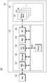
그리고, 메모리 시스템(110)은, 호스트(102)에 의해서 액세스되는 데이터를 저장하는 메모리 장치(150), 및 메모리 장치(150)로의 데이터 저장을 제어하는 컨트롤러(130)를 포함한다.The
여기서, 컨트롤러(130) 및 메모리 장치(150)는 하나의 반도체 장치로 집적될 수 있다. 일 예로, 컨트롤러(130) 및 메모리 장치(150)는 하나의 반도체 장치로 집적되어 SSD를 구성할 수 있다. 메모리 시스템(110)이 SSD로 이용되는 경우, 메모리 시스템(110)에 연결되는 호스트(102)의 동작 속도는 획기적으로 개선될 수 있다.Here, the
컨트롤러(130) 및 메모리 장치(150)는 하나의 반도체 장치로 집적되어, 메모리 카드를 구성할 수 있다. 예를 들면, 컨트롤러(130) 및 메모리 장치(150)는, 하나의 반도체 장치로 집적되어, PC 카드(PCMCIA: Personal Computer Memory Card International Association), 컴팩트 플래시 카드(CF), 스마트 미디어 카드(SM, SMC), 메모리 스틱, 멀티미디어 카드(MMC, RS-MMC, MMCmicro), SD 카드(SD, miniSD, microSD, SDHC), 유니버설 플래시 기억 장치(UFS) 등과 같은 메모리 카드를 구성할 수 있다.The
또 다른 일 예로, 메모리 시스템(110)은, 컴퓨터, UMPC (Ultra Mobile PC), 워크스테이션, 넷북(net-book), PDA (Personal Digital Assistants), 포터블(portable) 컴퓨터, 웹 타블렛(web tablet), 태블릿 컴퓨터(tablet computer), 무선 전화기(wireless phone), 모바일 폰(mobile phone), 스마트폰(smart phone), e-북(e-book), PMP(portable multimedia player), 휴대용 게임기, 네비게이션(navigation) 장치, 블랙박스(black box), 디지털 카메라(digital camera), DMB (Digital Multimedia Broadcasting) 재생기, 3차원 텔레비전(3-dimensional television), 스마트 텔레비전(smart television), 디지털 음성 녹음기(digital audio recorder), 디지털 음성 재생기(digital audio player), 디지털 영상 녹화기(digital picture recorder), 디지털 영상 재생기(digital picture player), 디지털 동영상 녹화기(digital video recorder), 디지털 동영상 재생기(digital video player), 데이터 센터를 구성하는 스토리지, 정보를 무선 환경에서 송수신할 수 있는 장치, 홈 네트워크를 구성하는 다양한 전자 장치들 중 하나, 컴퓨터 네트워크를 구성하는 다양한 전자 장치들 중 하나, 텔레매틱스 네트워크를 구성하는 다양한 전자 장치들 중 하나, RFID(radio frequency identification) 장치, 또는 컴퓨팅 시스템을 구성하는 다양한 구성 요소들 중 하나 등을 구성할 수 있다.As another example,
한편, 메모리 시스템(110)의 메모리 장치(150)는, 전원이 공급되지 않아도 저장된 데이터를 유지할 수 있으며, 특히 라이트(write) 동작을 통해 호스트(102)로부터 제공된 데이터를 저장하고, 리드(read) 동작을 통해 저장된 데이터를 호스트(102)로 제공한다. 그리고, 메모리 장치(150)는, 복수의 메모리 블록(memory block)들(152,154,156)을 포함하며, 각각의 메모리 블록들은, 복수의 페이지들(pages)을 포함하며, 또한 각각의 페이지들은, 복수의 워드라인(WL: Word Line)들이 연결된 복수의 메모리 셀들을 포함한다. 또한, 메모리 장치(150)는, 비휘발성 메모리 장치, 일 예로 플래시 메모리가 될 수 있으며, 이때 플래시 메모리는 3D 입체 스택(stack) 구조가 될 수 있다. 여기서, 메모리 장치(150)의 구조 및 메모리 장치(150)의 3D 입체 스택 구조에 대해서는, 이하 도 2 내지 도 11을 참조하여 보다 구체적으로 설명할 예정임으로, 여기서는 그에 관한 구체적인 설명을 생략하기로 한다.Meanwhile, the
그리고, 메모리 시스템(110)의 컨트롤러(130)는, 호스트(102)로부터의 요청에 응답하여 메모리 장치(150)를 제어한다. 예컨대, 컨트롤러(130)는, 메모리 장치(150)로부터 리드된 데이터를 호스트(102)로 제공하고, 호스트(102)로부터 제공된 데이터를 메모리 장치(150)에 저장하며, 이를 위해 컨트롤러(130)는, 메모리 장치(150)의 리드, 라이트, 프로그램(program), 이레이즈(erase) 등의 동작을 제어한다.The
보다 구체적으로 설명하면, 컨트롤러(130)는, 호스트 인터페이스(Host I/F) 유닛(132), 프로세서(Processor)(134), 에러 정정 코드(ECC: Error Correction Code) 유닛(138), 파워 관리 유닛(PMU: Power Management Unit)(140), 낸드 플래시 컨트롤러(NFC: NAND Flash Controller)(142), 및 메모리(Memory)(144)를 포함한다.More specifically, the
또한, 호스트 인터페이스 유닛(134)은, 호스트(102)의 커맨드(command) 및 데이터를 처리하며, USB(Universal Serial Bus), MMC(Multi-Media Card), PCI-E(Peripheral Component Interconnect-Express), SAS(Serial-attached SCSI), SATA(Serial Advanced Technology Attachment), PATA(Parallel Advanced Technology Attachment), SCSI(Small Computer System Interface), ESDI(Enhanced Small Disk Interface), IDE(Integrated Drive Electronics) 등과 같은 다양한 인터페이스 프로토콜들 중 적어도 하나를 통해 호스트(102)와 통신하도록 구성될 수 있다.In addition, the
아울러, ECC 유닛(138)은, 메모리 장치(150)에 저장된 데이터를 리드할 경우, 메모리 장치(150)로부터 리드된 데이터에 포함되는 에러를 검출 및 정정한다. 다시 말해, ECC 유닛(138)은, 메모리 장치(150)로부터 리드한 데이터에 대하여 에러 정정 디코딩을 수행한 후, 에러 정정 디코딩의 성공 여부를 판단하고 판단 결과에 따라 지시 신호를 출력하며, ECC 인코딩 과정에서 생성된 패리티(parity) 비트를 사용하여 리드된 데이터의 에러 비트를 정정할 수 있다. 이때, ECC 유닛(138)은, 에러 비트 개수가 정정 가능한 에러 비트 한계치 이상 발생하면, 에러 비트를 정정할 수 없으며, 에러 비트를 정정하지 못함에 상응하는 에러 정정 실패(fail) 신호를 출력할 수 있다.In addition, when reading data stored in the
여기서, ECC 유닛(138)은, LDPC(low density parity check) code, BCH(Bose, Chaudhri, Hocquenghem) code, turbo code, 리드-솔로몬 코드(Reed-Solomon code), convolution code, RSC(recursive systematic code), TCM(trellis-coded modulation), BCM(Block coded modulation) 등의 코디드 모듈레이션(coded modulation)을 사용하여 에러 정정을 수행할 수 있으며 이에 한정되는 것은 아니다. 또한, ECC 유닛(138)는 오류 정정을 위한 회로, 시스템 또는 장치를 모두 포함할 수 있다.Herein, the
그리고, PMU(140)는, 컨트롤러(130)의 파워, 즉 컨트롤러(130)에 포함된 구성 요소들의 파워를 제공 및 관리한다.The
또한, NFC(142)는, 컨트롤러(130)가 호스트(102)로부터의 요청에 응답하여 메모리 장치(150)를 제어하기 위해, 컨트롤러(130)와 메모리 장치(142) 간의 인터페이싱을 수행하는 메모리 인터페이스로서, 메모리 장치(142)가 플래시 메모리, 특히 일 예로 메모리 장치(142)가 낸드 플래시 메모리일 경우에, 프로세서(134)의 제어에 따라 메모리 장치(142)의 제어 신호를 생성하고 데이터를 처리한다.The
아울러, 메모리(144)는, 메모리 시스템(110) 및 컨트롤러(130)의 동작 메모리로, 메모리 시스템(110) 및 컨트롤러(130)의 구동을 위한 데이터를 저장한다. 보다 구체적으로 설명하면, 메모리(144)는, 컨트롤러(130)가 호스트(102)로부터의 요청에 응답하여 메모리 장치(150)를 제어, 예컨대 컨트롤러(130)가, 메모리 장치(150)로부터 리드된 데이터를 호스트(102)로 제공하고, 호스트(102)로부터 제공된 데이터를 메모리 장치(150)에 저장하며, 이를 위해 컨트롤러(130)가, 메모리 장치(150)의 리드, 라이트, 프로그램, 이레이즈(erase) 등의 동작을 제어할 경우, 이러한 동작을 메모리 시스템(110), 즉 컨트롤러(130)와 메모리 장치(150) 간이 수행하기 위해 필요한 데이터를 저장한다.The
여기서, 메모리(144)는, 휘발성 메모리로 구현될 수 있으며, 예컨대 정적 랜덤 액세스 메모리(SRAM: Static Random Access Memory), 또는 동적 랜덤 액세스 메모리(DRAM: Dynamic Random Access Memory) 등으로 구현될 수 있다. 또한, 메모리(144)는, 전술한 바와 같이, 호스트(102)와 메모리 장치(150) 간 데이터 라이트 및 리드 등의 동작을 수행하기 위해 필요한 데이터, 및 데이터 라이트 및 리드 등의 동작 수행 시의 데이터를 저장하며, 이러한 데이터 저장을 위해, 프로그램 메모리, 데이터 메모리, 라이트 버퍼, 리드 버퍼, 맵(map) 버퍼 등을 포함한다.The
그리고, 프로세서(134)는, 메모리 시스템(110)의 제반 동작을 제어하며, 호스트(102)로부터의 라이트 요청 또는 리드 요청에 응답하여, 메모리 장치(150)에 대한 라이트 동작 또는 리드 동작을 제어한다. 여기서, 프로세서(134)는, 메모리 시스템(110)의 제반 동작을 제어하기 위해 플래시 변환 계층(FTL: Flash Translation Layer, 이하 'FTL'이라 칭하기로 함)이라 불리는 펌웨어(firmware)를 구동한다. 또한, 프로세서(134)는, 마이크로프로세서 또는 중앙 처리 장치(CPU) 등으로 구현될 수 있다.The
아울러, 프로세서(134)에는, 메모리 장치(150)의 배드 관리(bad management), 예컨대 배드 블록 관리(bad block management)를 수행하기 위한 관리 유닛(도시하지 않음)이 포함되며, 관리 유닛은, 메모리 장치(150)에 포함된 복수의 메모리 블록들에서 배드 블록(bad block)을 확인한 후, 확인된 배드 블록을 배드 처리하는 배드 블록 관리를 수행한다. 여기서, 배드 관리, 다시 말해 배드 블록 관리는, 메모리 장치(150)가 플래쉬 메모리, 예컨대 낸드 플래시 메모리일 경우, 낸드의 특성으로 인해 데이터 라이트, 예컨대 데이터 프로그램(program) 시에 프로그램 실패(program fail)이 발생할 수 있으며, 프로그램 실패가 발생한 메모리 블록을 배드(bad) 처리한 후, 프로그램 실패된 데이터를 새로운 메모리 블록에 라이트, 즉 프로그램하는 것을 의미한다. 또한, 메모리 장치(150)가 3D 입체 스택 구조를 가질 경우에는, 프로그램 실패에 따라 해당 블록을 배드 블록으로 처리할 경우, 메모리 장치(150)의 사용 효율 및 메모리 시스템(100)의 신뢰성이 급격하게 저하되므로, 보다 신뢰성 있는 배드 블록 관리 수행이 필요하다. 그러면 이하에서는, 도 2 내지 도 11을 참조하여 본 발명의 실시 예에 따른 메모리 시스템에서의 메모리 장치에 대해서 보다 구체적으로 설명하기로 한다.The
도 2는 본 발명의 실시 예에 따른 메모리 시스템에서 메모리 장치의 일 예를 개략적으로 도시한 도면이고, 도 3은 본 발명의 실시 예에 따른 메모리 장치에서 메모리 블록들의 메모리 셀 어레이 회로를 개략적으로 도시한 도면이며, 도 4 내지 도 11은 본 발명의 실시 예에 따른 메모리 시스템에서 메모리 장치 구조를 개략적으로 도시한 도면으로, 메모리 장치가 3차원 비휘발성 메모리 장치로 구현될 경우의 구조를 개략적으로 도시한 도면이다.Figure 2 schematically illustrates an example of a memory device in a memory system according to an embodiment of the present invention, Figure 3 schematically illustrates a memory cell array circuit of memory blocks in a memory device according to an embodiment of the present invention. And FIGS. 4 to 11 are views schematically showing a structure of a memory device in a memory system according to an embodiment of the present invention, and schematically the structure when the memory device is implemented as a three-dimensional nonvolatile memory device Fig.
우선, 도 2를 참조하면, 메모리 장치(150)는, 복수의 메모리 블록들, 예컨대 블록0(Block0)(210), 블록1(Block1)(220), 블록2(Block2)(230), 및 블록N-1(BlockN-1)(240)을 포함하며, 각각의 블록들(210,220,230,240)은, 복수의 페이지들(Pages), 예컨대 2M개의 페이지들(2MPages)을 포함한다. 여기서, 설명의 편의를 위해, 복수의 메모리 블록들이 각각 2M개의 페이지들을 포함하는 것을 일 예로 하여 설명하지만, 복수의 메모리들은, 각각 M개의 페이지들을 포함할 수도 있다. 그리고, 각각의 페이지들은, 복수의 워드라인(WL: Word Line)들이 연결된 복수의 메모리 셀들을 포함한다.2, the
또한, 메모리 장치(150)는, 복수의 메모리 블록들을, 하나의 메모리 셀에 저장 또는 표현할 수 있는 비트의 수에 따라, 단일 레벨 셀(SLC: Single Level Cell) 메모리 블록 및 멀티 레벨 셀(MLC: Multi Level Cell) 메모리 블록 등으로 포함할 수 있다. 여기서, SLC 메모리 블록은, 하나의 메모리 셀에 1 비트 데이터를 저장하는 메모리 셀들에 의해 구현된 복수의 페이지들을 포함하며, 데이터 연산 성능이 빠르며 내구성이 높다. 그리고, MLC 메모리 블록은, 하나의 메모리 셀에 멀티 비트 데이터(예를 들면, 2 비트 이상)를 저장하는 메모리 셀들에 의해 구현된 복수의 페이지들을 포함하며, SLC 메모리 블록보다 큰 데이터 저장 공간을 가질 수, 다시 말해 고집적화 할 수 있다. 여기서, 하나의 메모리 셀에 3 비트 데이터를 저정할 수 있는 메모리 셀들에 의해 구현된 복수의 페이지들을 포함하는 MLC 메모리 블록을, 트리플 레벨 셀(TLC: Triple Level Cell) 메모리 블록으로 구분할 수도 있다.In addition, the
그리고, 각각의 블록들(210,220,230,240)은, 라이트 동작을 통해 호스트 장치로부터 제공된 데이터를 저장하고, 리드 동작을 통해 저장된 데이터를 호스트(102)로 제공한다.Each of the
다음으로, 도 3을 참조하면, 메모리 시스템(110)에서 메모리 장치(300)의 메모리 블록(330)은, 비트라인들(BL0 to BLm-1)에 각각 연결된 복수의 셀 스트링들(340)을 포함할 수 있다. 각 열(column)의 셀 스트링(340)은, 적어도 하나의 드레인 선택 트랜지스터(DST)와, 적어도 하나의 소스 선택 트랜지스터(SST)를 포함할 수 있다. 선택 트랜지스터들(DST, SST) 사이에는, 복수 개의 메모리 셀들, 또는, 메모리 셀 트랜지스터들(MC0 to MCn-1)이 직렬로 연결될 수 있다. 각각의 메모리 셀(MC0 to MCn-1)은, 셀 당 복수의 비트의 데이터 정보를 저장하는 멀티 레벨 셀(MLC: Multi-Level Cell)로 구성될 수 있다. 셀 스트링들(340)은 대응하는 비트라인들(BL0 to BLm-1)에 각각 전기적으로 연결될 수 있다.3,
여기서, 도 3은 낸드 플래시 메모리 셀로 구성된 메모리 블록(330)을 일 예로 도시하고 있으나, 본 발명의 실시 예에 따른 메모리 장치(300)의 메모리 블록(330)은, 낸드 플래시 메모리에만 국한되는 것은 아니라 노어 플래시 메모리(NOR-type Flash memory), 적어도 두 종류 이상의 메모리 셀들이 혼합된 하이브리드 플래시 메모리, 및 메모리 칩 내에 컨트롤러가 내장된 One-NAND 플래시 메모리 등으로도 구현될 수 있다. 반도체 장치의 동작 특성은 전하 저장층이 전도성 부유 게이트로 구성된 플래시 메모리 장치는 물론, 전하 저장층이 절연막으로 구성된 차지 트랩형 플래시(Charge Trap Flash; CTF)에도 적용될 수 있다.Here, FIG. 3 illustrates a
그리고, 메모리 장치(300)의 전압 공급부(310)는, 동작 모드에 따라서 각각의 워드라인들로 공급될 워드라인 전압들(예를 들면, 프로그램 전압, 리드 전압, 패스 전압 등)과, 메모리 셀들이 형성된 벌크(예를 들면, 웰 영역)로 공급될 전압을 제공할 수 있으며, 이때 전압 공급 회로(310)의 전압 발생 동작은 제어 회로(도시하지 않음)의 제어에 의해 수행될 수 있다. 또한, 전압 공급부(310)는, 다수의 리드 데이터를 생성하기 위해 복수의 가변 리드 전압들을 생성할 수 있으며, 제어 회로의 제어에 응답하여 메모리 셀 어레이의 메모리 블록들(또는 섹터들) 중 하나를 선택하고, 선택된 메모리 블록의 워드라인들 중 하나를 선택할 수 있으며, 워드라인 전압을 선택된 워드라인 및 비선택된 워드라인들로 각각 제공할 수 있다.The
아울러, 메모리 장치(300)의 리드/라이트(read/write) 회로(320)는, 제어 회로에 의해서 제어되며, 동작 모드에 따라 감지 증폭기(sense amplifier)로서 또는 라이트 드라이버(write driver)로서 동작할 수 있다. 예를 들면, 검증/정상 리드 동작의 경우 리드/라이트 회로(320)는, 메모리 셀 어레이로부터 데이터를 리드하기 위한 감지 증폭기로서 동작할 수 있다. 또한, 프로그램 동작의 경우 리드/라이트 회로(320)는, 메모리 셀 어레이에 저장될 데이터에 따라 비트라인들을 구동하는 라이트 드라이버로서 동작할 수 있다. 리드/라이트 회로(320)는, 프로그램 동작 시 셀 어레이에 라이트될 데이터를 버퍼(미도시)로부터 수신하고, 입력된 데이터에 따라 비트라인들을 구동할 수 있다. 이를 위해, 리드/라이트 회로(320)는, 열(column)들(또는 비트라인들) 또는 열쌍(column pair)(또는 비트라인 쌍들)에 각각 대응되는 복수 개의 페이지 버퍼들(PB)(322,324,326)을 포함할 수 있으며, 각각의 페이지 버퍼(page buffer)(322,324,326)에는 복수의 래치들(도시하지 않음)이 포함될 수 있다. 그러면 여기서, 도 4 내지 도 11을 참조하여 본 발명의 실시 예에 따른 메모리 시스템에서 메모리 장치가 3차원 비휘발성 메모리 장치로 구현될 경우의 메모리 장치에 대해서 보다 구체적으로 설명하기로 한다.In addition, the read /
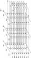
도 4를 참조하면, 메모리 장치(150)는, 전술한 바와 같이, 복수의 메모리 블록들(BLK 1 to BLKh)을 포함할 수 있다. 여기서, 도 4는, 도 3에 도시한 메모리 장치의 메모리 블록을 보여주는 블록도로서, 각 메모리 블록(BLK)은, 3차원 구조(또는 수직 구조)로 구현될 수 있다. 예를 들면, 각 메모리 블록(BLK)은 제1방향 내지 제3방향들, 예컨대 x-축 방향, y-축 방향, 및 z-축 방향을 따라 신장된 구조물들을 포함할 수 있다.Referring to FIG. 4, the
각 메모리 블록(BLK)은 제2방향을 따라 신장된 복수의 낸드 스트링들(NS)을 포함할 수 있다. 제1방향 및 제3방향들을 따라 복수의 낸드 스트링들(NS)이 제공될 수 있다. 각 낸드 스트링(NS)은 비트라인(BL), 적어도 하나의 스트링 선택라인(SSL), 적어도 하나의 접지 선택라인(GSL), 복수의 워드라인들(WL), 적어도 하나의 더미 워드라인(DWL), 그리고 공통 소스라인(CSL)에 연결될 수 있다. 즉, 각 메모리 블록은 복수의 비트라인들(BL), 복수의 스트링 선택라인들(SSL), 복수의 접지 선택라인들(GSL), 복수의 워드라인들(WL), 복수의 더미 워드라인들(DWL), 그리고 복수의 공통 소스라인(CSL)에 연결될 수 있다.Each memory block BLK may include a plurality of NAND strings NS extending along a second direction. A plurality of NAND strings NS may be provided along the first direction and the third direction. Each NAND string NS includes a bit line BL, at least one string select line SSL, at least one ground select line GSL, a plurality of word lines WL, at least one dummy word line DWL ), And a common source line (CSL). That is, each memory block includes a plurality of bit lines BL, a plurality of string select lines SSL, a plurality of ground select lines GSL, a plurality of word lines WL, a plurality of dummy word lines (DWL), and a plurality of common source lines (CSL).
그리고, 도 5 및 도 6을 참조하면, 메모리 장치(150)의 복수의 메모리 블록들에서 임의의 메모리 블록(BLKi)은, 제1방향 내지 제3방향들을 따라 신장된 구조물들을 포함할 수 있다. 여기서, 도 5는, 본 발명의 실시 예에 따른 메모리 장치가 제1구조의 3차원 비휘발성 메모리 장치로 구현될 경우의 구조를 개략적으로 도시한 도면이며, 도 4의 복수의 메모리 블록에서 제1구조로 구현된 임의의 메모리 블록(BLKi)을 도시한 사시도이고, 도 6은, 도 5의 메모리 블록(BLKi)을 임의의 제1선(I-I')에 따른 단면도이다.5 and 6, an arbitrary memory block BLKi in the plurality of memory blocks of the
우선, 기판(5111)이 제공될 수 있다. 예컨대, 기판(5111)은 제1타입 불순물로 도핑된 실리콘 물질을 포함할 수 있다. 예를 들면, 기판(5111)은 p-타입 불순물로 도핑된 실리콘 물질을 포함하거나, p-타입 웰(예를 들면, 포켓 p-웰)일 수 있고, p-타입 웰을 둘러싸는 n-타입 웰을 더 포함할 수 있다. 이하에서는 설명의 편의를 위해, 기판(5111)은 p-타입 실리콘인 것으로 가정하지만, 기판(5111)은 p-타입 실리콘으로 한정되지 않는다.First, a
그리고, 기판(5111) 상에, 제1방향을 따라 신장된 복수의 도핑 영역들(5311,5312,5313,5314)이 제공될 수 있다. 예를 들면, 복수의 도핑 영역들((5311,5312,5313,5314)은 기판(1111)과 상이한 제2타입을 가질 수 있다. 예를 들면, 복수의 도핑 영역들(5311,5312,5313,5314)은 n-타입을 가질 수 있다. 이하에서는 설명의 편의를 위해, 제1도핑 영역 내지 제4도핑 영역들(5311,5312,5313,5314)은, n-타입인 것으로 가정하지만, 제1도핑 영역 내지 제4도핑 영역들(5311,5312,5313,5314)은 n-타입인 것으로 한정되지 않는다.Then, on the
제1도핑 영역 및 제2도핑 영역들(5311,5312) 사이에 대응하는 기판(5111) 상의 영역에서, 제1방향을 따라 신장되는 복수의 절연 물질들(5112)이 제2방향을 따라 순차적으로 제공될 수 있다. 예를 들면, 복수의 절연 물질들(5112) 및 기판(5111)은 제2방향을 따라 미리 설정된 거리만큼 이격되어 제공될 수 있다. 예를 들면, 복수의 절연 물질들(5112)은 각각 제2방향을 따라 미리 설정된 거리만큼 이격되어 제공될 수 있다. 예컨대, 절연 물질들(5112)은 실리콘 산화물(Silicon Oxide)과 같은 절연 물질을 포함할 수 있다.In a region on the
제1도핑 영역 및 제2도핑 영역들(5311,5312) 사이에 대응하는 기판(5111) 상의 영역에서, 제1방향을 따라 순차적으로 배치되며 제2방향을 따라 절연 물질들(5112)을 관통하는 복수의 필라들(5113)이 제공될 수 있다. 예컨대, 복수의 필라들(5113) 각각은 절연 물질들(5112)을 관통하여 기판(5111)과 연결될 수 있다. 예컨대, 각 필라(5113)는 복수의 물질들로 구성될 수 있다. 예를 들면, 각 필라(1113)의 표면층(1114)은 제1타입으로 도핑된 실리콘 물질을 포함할 수 있다. 예를 들면, 각 필라(5113)의 표면층(5114)은 기판(5111)과 동일한 타입으로 도핑된 실리콘 물질을 포함할 수 있다. 이하에서는 설명의 편의를 위해, 각 필라(5113)의 표면층(5114)은 p-타입 실리콘을 포함하는 것으로 가정하지만, 각 필라(5113)의 표면층(5114)은 p-타입 실리콘을 포함하는 것으로 한정되지 않는다.Are sequentially disposed along the first direction in the region on the
각 필라(5113)의 내부층(5115)은 절연 물질로 구성될 수 있다. 예를 들면, 각 필라(5113)의 내부층(5115)은 실리콘 산화물(Silicon Oxide)과 같은 절연 물질로 충진될 수 있다.The
제1도핑 영역 및 제2도핑 영역들(5311,5312) 사이의 영역에서, 절연 물질들(5112), 필라들(5113), 그리고 기판(5111)의 노출된 표면을 따라 절연막(5116)이 제공될 수 있다. 예컨대, 절연막(5116)의 두께는 절연 물질들(5112) 사이의 거리의 1/2 보다 작을 수 있다. 즉, 절연 물질들(5112) 중 제1절연 물질의 하부 면에 제공된 절연막(5116), 그리고, 제1절연 물질 하부의 제2절연 물질의 상부 면에 제공된 절연막(5116) 사이에, 절연 물질들(5112) 및 절연막(5116) 이외의 물질이 배치될 수 있는 영역이 제공될 수 있다.The insulating
제1도핑 영역 및 제2도핑 영역들(5311,5312) 사이의 영역에서, 절연막(5116)의 노출된 표면 상에 도전 물질들(5211,5221,5231,5241,5251,5261,5271,5281,5291)이 제공될 수 있다. 예를 들면, 기판(5111)에 인접한 절연 물질(5112) 및 기판(5111) 사이에 제1방향을 따라 신장되는 도전 물질(5211)이 제공될 수 있다. 특히, 기판(5111)에 인접한 절연 물질(5112)의 하부 면의 절연막(5116) 및 기판(5111) 사이에, 제1방향으로 신장되는 도전 물질(5211)이 제공될 수 있다.In the region between the first doped region and the second
절연 물질들(5112) 중 특정 절연 물질 상부 면의 절연막(5116) 및 특정 절연 물질 상부에 배치된 절연 물질의 하부 면의 절연막(5116) 사이에, 제1방향을 따라 신장되는 도전 물질이 제공될 수 있다. 예컨대, 절연 물질들(5112) 사이에, 제1방향으로 신장되는 복수의 도전 물질들(5221,5231,5241,5251,5261,5271,5281)이 제공될 수 있다. 또한, 절연 물질들(5112) 상의 영역에 제1방향을 따라 신장되는 도전 물질(5291)이 제공될 수 있다. 예컨대, 제1방향으로 신장된 도전 물질들(5211,5221,5231,5241,5251,5261,5271,5281,5291)은 금속 물질일 수 있다. 예컨대, 제1방향으로 신장된 도전 물질들(5211,5221,5231,5241,5251,5261,5271,5281,5291)은 폴리 실리콘 등과 같은 도전 물질일 수 있다.A conductive material extending along the first direction is provided between the insulating
제2도핑 영역 및 제3도핑 영역들(5312,5313) 사이의 영역에서, 제1도핑 영역 및 제2도핑 영역들(5311,5312) 상의 구조물과 동일한 구조물이 제공될 수 있다. 예컨대, 제2도핑 영역 및 제3도핑 영역들(5312,5313) 사이의 영역에서, 제1방향으로 신장되는 복수의 절연 물질들(5112), 제1방향을 따라 순차적으로 배치되며 제3방향을 따라 복수의 절연 물질들(5112)을 관통하는 복수의 필라들(5113), 복수의 절연 물질들(5112) 및 복수의 필라들(5113)의 노출된 표면에 제공되는 절연막(5116), 그리고, 제1방향을 따라 신장되는 복수의 도전 물질들(5212,5222,5232,5242,5252,5262,5272,5282,5292)이 제공될 수 있다.In the region between the second doped region and the third
제3도핑 영역 및 제4도핑 영역들(5313,5314) 사이의 영역에서, 제1도핑 영역 및 제2도핑 영역들(5311,5312) 상의 구조물과 동일한 구조물이 제공될 수 있다. 예컨대, 제3도핑 영역 및 제4도핑 영역들(5312,5313) 사이의 영역에서, 제1방향으로 신장되는 복수의 절연 물질들(5112), 제1방향을 따라 순차적으로 배치되며 제3방향을 따라 복수의 절연 물질들(5112)을 관통하는 복수의 필라들(5113), 복수의 절연 물질들(5112) 및 복수의 필라들(5113)의 노출된 표면에 제공되는 절연막(5116), 그리고 제1방향을 따라 신장되는 복수의 도전 물질들(5213,5223,5243,5253,5263,5273,5283,5293)이 제공될 수 있다.In the region between the third doped region and the fourth
복수의 필라들(5113) 상에 드레인들(5320)이 각각 제공될 수 있다. 예컨대, 드레인들(5320)은 제2타입으로 도핑된 실리콘 물질들일 수 있다. 예를 들면, 드레인들(5320)은 n-타입으로 도핑된 실리콘 물질들일 수 있다. 이하에서는 설명의 편의를 위해, 드레인들(5320)는 n-타입 실리콘을 포함하는 것으로 가정하지만, 드레인들(5320)은 n-타입 실리콘을 포함하는 것으로 한정되지 않는다. 예컨대, 각 드레인(5320)의 폭은 대응하는 필라(5113)의 폭 보다 클 수 있다. 예를 들면, 각 드레인(5320)은 대응하는 필라(5113)의 상부면에 패드 형태로 제공될 수 있다.
드레인들(5320) 상에, 제3방향으로 신장된 도전 물질들(5331,5332,5333)이 제공될 수 있다. 도전 물질들(5331,5332,5333)은 제1방향을 따라 순차적으로 배치될 수 있다. 도전 물질들(5331,5332,5333) 각각은 대응하는 영역의 드레인들(5320)과 연결될 수 있다. 예컨대, 드레인들(5320) 및 제3방향으로 신장된 도전 물질(5333)은 각각 콘택 플러그들(contact plug)을 통해 연결될 수 있다. 예컨대, 제3방향으로 신장된 도전 물질들(5331,5332,5333)은 금속 물질일 수 있다. 예컨대, 제3방향으로 신장된 도전 물질들(5331,5332,53333)은 폴리 실리콘 등과 같은 도전 물질일 수 있다.On the
도 5 및 도 6에서, 각 필라(5113)는 절연막(5116)의 인접한 영역 및 제1방향을 따라 신장되는 복수의 도체라인들(5211 내지 5291, 5212 내지 5292, 및 5213 내지 5293) 중 인접한 영역과 함께 스트링을 형성할 수 있다. 예를 들면, 각 필라(5113)는 절연막(5116)의 인접한 영역 및 제1방향을 따라 신장되는 복수의 도체라인들(5211 내지 5291, 5212 내지 5292, 및 5213 내지 5293) 중 인접한 영역과 함께 낸드 스트링(NS)을 형성할 수 있다. 낸드 스트링(NS)은 복수의 트랜지스터 구조들(TS)을 포함할 수 있다.5 and 6, each of the
그리고, 도 7을 참조하면, 도 6에 도시한 트랜지스터 구조(TS)에서의 절연막(5116)은, 제1서브 절연막 내지 제3서브 절연막들(5117,5118,5119)을 포함할 수 있다. 여기서, 도 7은, 도 6의 트랜지스터 구조(TS)를 보여주는 단면도이다.7, the insulating
필라(5113)의 p-타입 실리콘(5114)은 바디(body)로 동작할 수 있다. 필라(5113)에 인접한 제1서브 절연막(5117)은 터널링 절연막으로 동작할 수 있으며, 열산화막을 포함할 수 있다.The p-
제2서브 절연막(5118)은 전하 저장막으로 동작할 수 있다. 예를 들면, 제2서브 절연막(5118)은 전하 포획층으로 동작할 수 있으며, 질화막 또는 금속 산화막(예컨대, 알루미늄 산화막, 하프늄 산화막 등)을 포함할 수 있다.The
도전 물질(5233)에 인접한 제3 서브 절연막(5119)은 블로킹 절연막으로 동작할 수 있다. 예를 들면, 제1방향으로 신장된 도전 물질(5233)과 인접한 제3서브 절연막(5119)은 단일층 또는 다층으로 형성될 수 있다. 제3서브 절연막(5119)은 제1서브 절연막 및 제2서브 절연막들(5117,5118)보다 높은 유전상수를 갖는 고유전막(예컨대, 알루미늄 산화막, 하프늄 산화막 등)일 수 있다.The
도전 물질(5233)은 게이트(또는 제어 게이트)로 동작할 수 있다. 즉, 게이트(또는 제어 게이트(5233)), 블로킹 절연막(5119), 전하 저장막(5118), 터널링 절연막(5117), 및 바디(5114)는, 트랜지스터(또는 메모리 셀 트랜지스터 구조)를 형성할 수 있다. 예컨대, 제1서브 절연막 내지 제3서브 절연막들(5117,5118,5119)은 ONO(oxide-nitride-oxide)를 구성할 수 있다. 이하에서는 설명의 편의를 위해, 필라(5113)의 p-타입 실리콘(5114)을 제2방향의 바디라 칭하기로 한다.
메모리 블록(BLKi)은 복수의 필라들(5113)을 포함할 수 있다. 즉, 메모리 블록(BLKi)은 복수의 낸드 스트링들(NS)을 포함할 수 있다. 보다 구체적으로 설명하면, 메모리 블록(BLKi)은 제2방향(또는 기판과 수직한 방향)으로 신장된 복수의 낸드 스트링들(NS)을 포함할 수 있다.The memory block BLKi may include a plurality of
각 낸드 스트링(NS)은 제2방향을 따라 배치되는 복수의 트랜지스터 구조들(TS)을 포함할 수 있다. 각 낸드 스트링(NS)의 복수의 트랜지스터 구조들(TS) 중 적어도 하나는 스트링 선택 트랜지스터(SST)로 동작할 수 있다. 각 낸드 스트링(NS)의 복수의 트랜지스터 구조들(TS) 중 적어도 하나는 접지 선택 트랜지스터(GST)로 동작할 수 있다.Each NAND string NS may include a plurality of transistor structures TS disposed along a second direction. At least one of the plurality of transistor structures TS of each NAND string NS may operate as a string selection transistor (SST). At least one of the plurality of transistor structures TS of each NAND string NS may operate as a ground selection transistor (GST).
게이트들(또는 제어 게이트들)은 제1방향으로 신장된 도전 물질들(5211 내지 5291, 5212 내지 5292, 및 5213 내지 5293)에 대응할 수 있다. 즉, 게이트들(또는 제어 게이트들)은 제1방향으로 신장되어 워드라인들, 그리고 적어도 두 개의 선택라인들(예를 들면, 적어도 하나의 스트링 선택라인(SSL) 및 적어도 하나의 접지 선택라인(GSL))을 형성할 수 있다.The gates (or control gates) may correspond to the
제3방향으로 신장된 도전 물질들(5331,5332,5333)은 낸드 스트링들(NS)의 일단에 연결될 수 있다. 예컨대, 제3방향으로 신장된 도전 물질들(5331,5332,5333)은 비트라인들(BL)로 동작할 수 있다. 즉, 하나의 메모리 블록(BLKi)에서, 하나의 비트라인(BL)에 복수의 낸드 스트링들(NS)이 연결될 수 있다.The
제1방향으로 신장된 제2타입 도핑 영역들(5311,5312,5313,5314)이 낸드 스트링들(NS)의 타단에 제공될 수 있다. 제1방향으로 신장된 제2타입 도핑 영역들(5311,5312,5313,5314)은 공통 소스라인들(CSL)로 동작할 수 있다.Second type doped
즉, 메모리 블록(BLKi)은 기판(5111)에 수직한 방향(제2방향)으로 신장된 복수의 낸드 스트링들(NS)을 포함하며, 하나의 비트라인(BL)에 복수의 낸드 스트링들(NS)이 연결되는 낸드 플래시 메모리 블록(예를 들면, 전하 포획형)으로 동작할 수 있다.That is, the memory block BLKi includes a plurality of NAND strings NS extending in a direction perpendicular to the substrate 5111 (second direction), and a plurality of NAND strings NAND flash memory block (e.g., charge trapping type) to which the NAND flash memory is connected.
도 5 내지 도 7에서는, 제1방향으로 신장되는 도체라인들(5211 내지 5291, 5212 내지 5292, 및 5213 내지 5293)이 9개의 층에 제공되는 것으로 설명하였지만, 제1방향으로 신장되는 도체라인들(5211 내지 5291, 5212 내지 5292, 및 5213 내지 5293)이 9개의 층에 제공되는 것으로 한정되지 않는다. 예를 들면, 제1방향으로 신장되는 도체라인들은 8개의 층, 16개의 층, 또는 복수의 층에 제공될 수 있다. 즉, 하나의 낸드 스트링(NS)에서, 트랜지스터는 8개, 16개, 또는 복수 개일 수 있다.5 to 7,
전술한 도 5 내지 도 7에서는, 하나의 비트라인(BL)에 3 개의 낸드 스트링들(NS)이 연결되는 것으로 설명하였으나, 하나의 비트라인(BL)에 3개의 낸드 스트링들(NS)이 연결되는 것으로 한정되지 않는다. 예컨대, 메모리 블록(BLKi)에서, 하나의 비트라인(BL)에 m 개의 낸드 스트링들(NS)이 연결될 수 있다. 이때, 하나의 비트라인(BL)에 연결되는 낸드 스트링들(NS)의 수만큼, 제1방향으로 신장되는 도전 물질들(5211 내지 5291, 5212 내지 5292, 및 5213 내지 5293)의 수 및 공통 소스라인들(5311,5312,5313,5314)의 수 또한 조절될 수 있다.5 to 7, three NAND strings NS are connected to one bit line BL. However, three NAND strings NS may be connected to one bit line BL, . For example, in the memory block BLKi, m NAND strings NS may be connected to one bit line BL. At this time, the number of conductive materials (5211 to 5291, 5212 to 5292, and 5213 to 5293) extending in the first direction by the number of NAND strings (NS) connected to one bit line (BL) The number of
또한, 도 5 내지 도 7에서는, 제1방향으로 신장된 하나의 도전 물질에 3 개의 낸드 스트링들(NS)이 연결되는 것으로 설명하였으나, 제1방향으로 신장된 하나의 도전 물질에 3 개의 낸드 스트링들(NS)이 연결되는 것으로 한정되지 않는다. 예를 들면, 제1방향으로 신장된 하나의 도전 물질에, n 개의 낸드 스트링들(NS)이 연결될 수 있다. 이때, 제1방향으로 신장된 하나의 도전 물질에 연결되는 낸드 스트링들(NS)의 수만큼, 비트라인들(5331,5332,5333)의 수 또한 조절될 수 있다.5 to 7, three NAND strings NS are connected to one conductive material extending in the first direction. However, in the case where one conductive material extended in the first direction has three NAND strings NS are connected to each other. For example, n conductive n-strings NS may be connected to one conductive material extending in a first direction. At this time, the number of
도 8을 참조하면, 메모리 장치(150)의 복수의 블록들에서 제1구조로 구현된 임의의 블록(BLKi)에는, 제1비트라인(BL1) 및 공통 소스라인(CSL) 사이에 낸드 스트링들(NS11 to NS31)이 제공될 수 있다. 여기서, 도 8은, 도 5 내지 도 7에서 설명한 제1구조로 구현된 메모리 블록(BLKi)의 등가 회로를 도시한 회로도이다. 그리고, 제1비트라인(BL1)은 제3방향으로 신장된 도전 물질(5331)에 대응할 수 있다. 제2비트라인(BL2) 및 공통 소스라인(CSL) 사이에 낸드 스트링들(NS12, NS22, NS32)이 제공될 수 있다. 제2비트라인(BL2)은 제3방향으로 신장된 도전 물질(5332)에 대응할 수 있다. 제3비트라인(BL3) 및 공통 소스라인(CSL) 사이에, 낸드 스트링들(NS13, NS23, NS33)이 제공될 수 있다. 제3비트라인(BL3)은 제3방향으로 신장된 도전 물질(5333)에 대응할 수 있다.8, in any block BLKi implemented with the first structure in the plurality of blocks of the
각 낸드 스트링(NS)의 스트링 선택 트랜지스터(SST)는 대응하는 비트라인(BL)과 연결될 수 있다. 각 낸드 스트링(NS)의 접지 선택 트랜지스터(GST)는 공통 소스라인(CSL)과 연결될 수 있다. 각 낸드 스트링(NS)의 스트링 선택 트랜지스터(SST) 및 접지 선택 트랜지스터(GST) 사이에 메모리 셀들(MC)이 제공될 수 있다.The string selection transistor SST of each NAND string NS may be connected to the corresponding bit line BL. The ground selection transistor GST of each NAND string NS can be connected to the common source line CSL. Memory cells MC may be provided between the string selection transistor SST and the ground selection transistor GST of each NAND string NS.
이하에서는 설명의 편의를 위해, 행(row) 및 열(column)) 단위로 낸드 스트링들(NS)을 정의할 수 있으며, 하나의 비트라인에 공통으로 연결된 낸드 스트링들(NS)은 하나의 열을 형성할 수 있음을, 일 예로 하여 설명하기로 한다. 예를 들면, 제1비트라인(BL1)에 연결된 낸드 스트링들(NS11 내지 NS31)은 제1열에 대응할 수 있고, 제2비트라인(BL2)에 연결된 낸드 스트링들(NS12 내지 NS32)은 제2열에 대응할 수 있으며, 제3비트라인(BL3)에 연결된 낸드 스트링들(NS13 내지 NS33)은 제3열에 대응할 수 있다. 하나의 스트링 선택라인(SSL)에 연결되는 낸드 스트링들(NS)은 하나의 행을 형성할 수 있다. 예를 들면, 제1스트링 선택라인(SSL1)에 연결된 낸드 스트링들(NS11 내지 NS13)은 제1행을 형성할 수 있고, 제2스트링 선택라인(SSL2)에 연결된 낸드 스트링들(NS21 내지 NS23)은 제2행을 형성할 수 있으며, 제3스트링 선택라인(SSL3)에 연결된 낸드 스트링들(NS31 내지 NS33)은 제3행을 형성할 수 있다.Hereinafter, for convenience of explanation, NAND strings NS may be defined in units of a row and a column, and NAND strings NS connected in common to one bit line may be defined as one column As will be described below. For example, the NAND strings NS11 to NS31 connected to the first bit line BL1 may correspond to the first column, and the NAND strings NS12 to NS32 connected to the second bit line BL2 may correspond to the second column And the NAND strings NS13 to NS33 connected to the third bit line BL3 may correspond to the third column. The NAND strings NS connected to one string select line (SSL) can form one row. For example, the NAND strings NS11 through NS13 connected to the first string selection line SSL1 may form a first row, the NAND strings NS21 through NS23 connected to the second string selection line SSL2, And the NAND strings NS31 to NS33 connected to the third string selection line SSL3 may form the third row.
또한, 각 낸드 스트링(NS)에서, 높이가 정의될 수 있다. 예컨대, 각 낸드 스트링(NS)에서, 접지 선택 트랜지스터(GST)에 인접한 메모리 셀(MC1)의 높이는 1이다. 각 낸드 스트링(NS)에서, 스트링 선택 트랜지스터(SST)에 인접할수록 메모리 셀의 높이는 증가할 수 있다. 각 낸드 스트링(NS)에서, 스트링 선택 트랜지스터(SST)에 인접한 메모리 셀(MC7)의 높이는 7이다.Further, in each NAND string NS, a height can be defined. For example, in each NAND string NS, the height of the memory cell MC1 adjacent to the ground selection transistor GST is one. In each NAND string NS, the height of the memory cell may increase as the string selection transistor SST is adjacent to the string selection transistor SST. In each NAND string NS, the height of the memory cell MC7 adjacent to the string selection transistor SST is seven.
그리고, 동일한 행의 낸드 스트링들(NS)의 스트링 선택 트랜지스터들(SST)은 스트링 선택라인(SSL)을 공유할 수 있다. 상이한 행의 낸드 스트링들(NS)의 스트링 선택 트랜지스터들(SST)은 상이한 스트링 선택라인들(SSL1, SSL2, SSL3)에 각각 연결될 수 있다.Then, the string selection transistors SST of the NAND strings NS in the same row can share the string selection line SSL. The string selection transistors SST of the NAND strings NS of the different rows can be connected to the different string selection lines SSL1, SSL2 and SSL3, respectively.
아울러, 동일한 행의 낸드 스트링들(NS)의 동일한 높이의 메모리 셀들은 워드라인(WL)을 공유할 수 있다. 즉, 동일한 높이에서, 상이한 행의 낸드 스트링들(NS)의 메모리 셀들(MC)에 연결된 워드라인들(WL)은 공통으로 연결될 수 있다. 동일한 행의 낸드 스트링들(NS)의 동일한 높이의 더미 메모리 셀들(DMC)은 더미 워드라인(DWL)을 공유할 수 있다. 즉, 동일한 높이에서, 상이한 행의 낸드 스트링들(NS)의 더미 메모리 셀들(DMC)에 연결된 더미 워드라인들(DWL)은 공통으로 연결될 수 있다.In addition, memory cells at the same height of the NAND strings NS in the same row can share the word line WL. That is, at the same height, the word lines WL connected to the memory cells MC of the NAND strings NS of different rows can be connected in common. The dummy memory cells DMC of the same height of the NAND strings NS in the same row can share the dummy word line DWL. That is, at the same height, the dummy word lines DWL connected to the dummy memory cells DMC of the NAND strings NS of the different rows can be connected in common.
예컨대, 워드라인들(WL) 또는 더미 워드라인들(DWL)은 제1방향으로 신장되는 도전 물질들(5211 내지 5291, 5212 내지 5292, 및 5213 내지 5293)이 제공되는 층에서 공통으로 연결될 수 있다. 예컨대, 제1방향으로 신장되는 도전 물질들(5211 내지 5291, 5212 내지 5292, 및 5213 내지 5293)은 콘택을 통해 상부 층에 연결될 수 있다. 상부 층에서 제1방향으로 신장되는 도전 물질들(5211 내지 5291, 5212 내지 5292, 및 5213 내지 5293)이 공통으로 연결될 수 있다. 즉, 동일한 행의 낸드 스트링들(NS)의 접지 선택 트랜지스터들(GST)은 접지 선택라인(GSL)을 공유할 수 있다. 그리고, 상이한 행의 낸드 스트링들(NS)의 접지 선택 트랜지스터들(GST)은 접지 선택라인(GSL)을 공유할 수 있다. 다시 말해, 낸드 스트링들(NS11 내지 NS13, NS21 내지 NS23, 및 NS31 내지 NS33)은 접지 선택라인(GSL)에 공통으로 연결될 수 있다.For example, the word lines WL or the dummy word lines DWL may be connected in common in the layer provided with the
공통 소스라인(CSL)은 낸드 스트링들(NS)에 공통으로 연결될 수 있다. 예를 들면, 기판(5111) 상의 활성 영역에서, 제1도핑 영역 내지 제4도핑 영역들(5311,5312,5313,5314)이 연결될 수 있다. 예를 들면, 제1도핑 영역 내지 제4도핑 영역들(5311,5312,5313,5314)은 콘택을 통해 상부 층에 연결될 수 있고, 또한 상부 층에서 제1도핑 영역 내지 제4도핑 영역들(5311,5312,5313,5314)이 공통으로 연결될 수 있다.The common source line CSL may be connected in common to the NAND strings NS. For example, in the active region on the
즉, 도 8에 도시된 바와 같이, 동일 깊이의 워드라인들(WL)은 공통으로 연결될 수 있다. 따라서, 특정 워드라인(WL)이 선택될 때, 특정 워드라인(WL)에 연결된 모든 낸드 스트링들(NS)이 선택될 수 있다. 상이한 행의 낸드 스트링들(NS)은 상이한 스트링 선택라인(SSL)에 연결될 수 있다. 따라서, 스트링 선택라인들(SSL1 내지 SSL3)을 선택함으로써, 동일 워드라인(WL)에 연결된 낸드 스트링들(NS) 중 비선택 행의 낸드 스트링들(NS)이 비트라인들(BL1 내지 BL3)로부터 분리될 수 있다. 즉, 스트링 선택라인들(SSL1 내지 SSL3)을 선택함으로써, 낸드 스트링들(NS)의 행이 선택될 수 있다. 그리고, 비트라인들(BL1 내지 BL3)을 선택함으로써, 선택 행의 낸드 스트링들(NS)이 열 단위로 선택될 수 있다.That is, as shown in FIG. 8, the word lines WL of the same depth can be connected in common. Thus, when a particular word line WL is selected, all NAND strings NS connected to a particular word line WL can be selected. NAND strings NS in different rows may be connected to different string select lines SSL. Thus, by selecting the string selection lines SSL1 to SSL3, the NAND strings NS of unselected rows among the NAND strings NS connected to the same word line WL are selected from the bit lines BL1 to BL3 Can be separated. That is, by selecting the string selection lines SSL1 to SSL3, a row of NAND strings NS can be selected. Then, by selecting the bit lines BL1 to BL3, the NAND strings NS of the selected row can be selected in units of columns.
각 낸드 스트링(NS)에서, 더미 메모리 셀(DMC)이 제공될 수 있다. 더미 메모리 셀(DMC) 및 접지 선택라인(GST) 사이에 제1메모리 셀 내지 제3메모리 셀들(MC1 내지 MC3)이 제공될 수 있다.In each NAND string NS, a dummy memory cell DMC may be provided. The first to third memory cells MC1 to MC3 may be provided between the dummy memory cell DMC and the ground selection line GST.
더미 메모리 셀(DMC) 및 스트링 선택라인(SST) 사이에 제4메모리 셀 내지 제6메모리 셀들(MC4 내지 MC6)이 제공될 수 있다. 여기서, 각 낸드 스트링(NS)의 메모리 셀들(MC)은, 더미 메모리 셀(DMC)에 의해 메모리 셀 그룹들로 분할될 수 있으며, 분할된 메모리 셀 그룹들 중 접지 선택 트랜지스터(GST)에 인접한 메모리 셀들(예를 들면, MC1 to MC3)을 하부 메모리 셀 그룹이라 할 수 있고, 분할된 메모리 셀 그룹들 중 스트링 선택 트랜지스터(SST)에 인접한 메모리 셀들(예를 들면, MC4 내지 MC6)을 상부 메모리 셀 그룹이라 할 수 있다. 그러면 이하에서는, 도 9 내지 도 11을 참조하여 본 발명의 실시 예에 따른 메모리 시스템에서 메모리 장치가 제1구조와 다른 구조의 3차원 비휘발성 메모리 장치로 구현될 경우에 대해 보다 구체적으로 설명하기로 한다.The fourth to sixth memory cells MC4 to MC6 may be provided between the dummy memory cell DMC and the string selection line SST. Here, the memory cells MC of each NAND string NS can be divided into memory cell groups by the dummy memory cells DMC, and the memory cells MC of the divided memory cell groups adjacent to the ground selection transistor GST (For example, MC1 to MC3) may be referred to as a lower memory cell group, and memory cells (for example, MC4 to MC6) adjacent to the string selection transistor SST among the divided memory cell groups may be referred to as an upper memory cell Group. Hereinafter, with reference to FIGS. 9 to 11, the memory device according to the embodiment of the present invention will be described in more detail when the memory device is implemented as a three-dimensional nonvolatile memory device having a structure different from that of the first structure do.
도 9 및 도 10을 참조하면, 메모리 장치(150)의 복수의 메모리 블록들에서 제2구조로 구현된 임의의 메모리 블록(BLKj)은, 제1방향 내지 제3방향들을 따라 신장된 구조물들을 포함할 수 있다. 여기서, 도 9는, 본 발명의 실시 예에 따른 메모리 장치가 앞선 도 5 내지 도 8에서 설명한 제1구조와 다른 제2구조의 3차원 비휘발성 메모리 장치로 구현될 경우의 구조를 개략적으로 도시한 도면이며, 도 4의 복수의 메모리 블록에서 제2구조로 구현된 임의의 메모리 블록(BLKj)을 도시한 사시도이고, 도 10은, 도 9의 메모리 블록(BLKj)을 임의의 제2선(Ⅶ-Ⅶ')에 따른 단면도이다.9 and 10, an arbitrary memory block BLKj implemented in the second structure in the plurality of memory blocks of the
우선, 기판(6311)이 제공될 수 있다. 예컨대, 기판(6311)은 제1타입 불순물로 도핑된 실리콘 물질을 포함할 수 있다. 예를 들면, 기판(6311)은 p-타입 불순물로 도핑된 실리콘 물질을 포함하거나, p-타입 웰(예를 들면, 포켓 p-웰)일 수 있고, p-타입 웰을 둘러싸는 n-타입 웰을 더 포함할 수 있다. 이하에서는 설명의 편의를 위해, 기판(6311)은 p-타입 실리콘인 것으로 가정하지만, 기판(6311)은 p-타입 실리콘으로 한정되지 않는다.First, a
그리고, 기판(6311) 상에, x-축 방향 및 y-축 방향으로 신장되는 제1도전 물질 내지 제4도전 물질들(6321,6322,6323,6324)이 제공된다. 여기서, 제1도전 물질 내지 제4도전 물질들(6321,6322,6323,6324)은 z-축 방향을 따라 특정 거리만큼 이격되어 제공된다.Then, on the
또한, 기판(6311) 상에 x-축 방향 및 y-축으로 신장되는 제5도전 물질 내지 제8도전 물질들(6325,6326,6327,6328)이 제공된다. 여기서, 제5도전 물질 내지 제8도전 물질들(6325,6326,6327,6328)은 z-축 방향을 따라 특정 거리만큼 이격되어 제공된다. 그리고, 제5도전 물질 내지 제8도전 물질들(6325,6326,6327,6328)은 y-축 방향을 따라 제1도전 물질 내지 제4도전 물질들(6321,6322,6323,6324)과 이격되어 제공된다.Further, fifth to eighth
아울러, 제1도전 물질 내지 제4도전 물질들(6321,6322,6323,6324)을 관통하는 복수의 하부 필라들이 제공된다. 각 하부 필라(DP)는 z-축 방향을 따라 신장된다. 또한, 제5도전 물질 내지 제8도전 물질들(6325,6326,6327,6328)을 관통하는 복수의 상부 필라들이 제공된다. 각 상부 필라(UP)는 z-축 방향을 따라 신장된다.In addition, a plurality of lower pillars penetrating the first to fourth
하부 필라(DP) 및 상부 필라(UP) 각각은 내부 물질(6361), 중간층(6362) 및 표면층(6363)을 포함한다. 여기서, 도 5 및 도 6에서 설명한 바와 같이, 중간층(6362)은 셀 트랜지스터의 채널로서 동작할 것이다. 표면층(6363)은 블로킹 절연막, 전하 저장막 및 터널링 절연막을 포함할 것이다.Each of the lower pillars DP and upper pillars UP includes an
하부 필라(DP) 및 상부 필라(UP)는 파이프 게이트(PG)를 통해 연결된다. 파이프 게이트(PG)는 기판(6311) 내에 배치될 수 있으며, 일 예로, 파이프 게이트(PG)는 하부 필라(DP) 및 상부 필라(UP)와 동일한 물질들을 포함할 수 있다.The lower pillar DP and the upper pillar UP are connected via a pipe gate PG. The pipe gate PG may be disposed within the
하부 필라(DP)의 상부에, x-축 방향 및 y-축 방향으로 신장되는 제 2 타입의 도핑 물질(6312)이 제공된다. 예컨대, 제2타입의 도핑 물질(6312)은 n-타입의 실리콘 물질을 포함할 수 있다. 제2타입의 도핑 물질(6312)은 공통 소스라인(CSL)으로서 동작한다.On top of the lower pillar DP is provided a second type of
상부 필라(UP)의 상부에 드레인(6340)이 제공된다. 예컨대, 드레인(6340)은 n-타입의 실리콘 물질을 포함할 수 있다. 그리고, 드레인들의 상부에 y-축 방향으로 신장되는 제1상부 도전 물질 및 제2상부 도전 물질들(6351,6352)이 제공된다.A
제1상부 도전 물질 및 제2상부 도전 물질들(6351,6352)은 x-축 방향을 따라 이격되어 제공된다. 예컨대, 제1상부 도전 물질 및 제2상부 도전 물질들(6351,6352)은 금속으로서 형성될 수 있으며, 일 예로, 제1상부 도전 물질 및 제2상부 도전 물질들(6351,6352)과 드레인들은 콘택 플러그들을 통해 연결될 수 있다. 제1상부 도전 물질 및 제2상부 도전 물질들(6351,6352)은 각각 제1비트라인 및 제2비트라인들(BL1, BL2)로 동작한다.The first upper conductive material and the second upper
제1도전 물질(6321)은 소스 선택라인(SSL)으로 동작하고, 제2도전 물질(6322)은 제1더미 워드라인(DWL1)으로 동작하며, 제3도전 물질 및 제4도전 물질들(6323,6324)은 각각 제1메인 워드라인 및 제2메인 워드라인들(MWL1, MWL2)로 동작한다. 그리고, 제5도전 물질 및 제6도전 물질들(6325,6326)은 각각 제3메인 워드라인 및 제4메인 워드라인들(MWL3, MWL4)로 동작하고, 제7도전 물질(6327)은 제2더미 워드라인(DWL2)으로 동작하며, 제8도전 물질(6328)은 드레인 선택라인(DSL)로서 동작한다.The first
하부 필라(DP), 그리고 하부 필라(DP)에 인접한 제1도전 물질 내지 제4도전 물질들(6321,6322,6323,6324)은 하부 스트링을 구성한다. 상부 필라(UP), 그리고 상부 필라(UP)에 인접한 제5도전 물질 내지 제8도전 물질들(6325,6326,6327,6328)은 상부 스트링을 구성한다. 하부 스트링 및 상부 스트링은 파이프 게이트(PG)를 통해 연결된다. 하부 스트링의 일단은 공통 소스라인(CSL)으로 동작하는 제2타입의 도핑 물질(6312)에 연결된다. 상부 스트링의 일단은 드레인(6320)을 통해 해당 비트라인에 연결된다. 하나의 하부 스트링 및 하나의 상부 스트링은 제2타입의 도핑 물질(6312)과 해당 비트라인 사이에 연결된 하나의 셀 스트링을 구성할 것이다.And the first to fourth
즉, 하부 스트링은 소스 선택 트랜지스터(SST), 제1더미 메모리 셀(DMC1), 그리고 제1메인 메모리 셀 및 제2메인 메모리 셀들(MMC1, MMC2)을 포함할 것이다. 그리고, 상부 스트링은 제3메인 메모리 셀 및 제4메인 메모리 셀들(MMC3, MMC4), 제2더미 메모리 셀(DMC2), 그리고 드레인 선택 트랜지스터(DST)를 포함할 것이다.That is, the lower string will include a source select transistor (SST), a first dummy memory cell (DMC1), and a first main memory cell and a second main memory cell (MMC1, MMC2). The upper string will include a third main memory cell and fourth main memory cells MMC3 and MMC4, a second dummy memory cell DMC2, and a drain select transistor DST.
한편, 도 9 및 도 10에서 상부 스트림 및 하부 스트링은, 낸드 스트링(NS)을 형성할 수 있으며, 낸드 스트링(NS)은 복수의 트랜지스터 구조들(TS)을 포함할 수 있다. 여기서, 도 9 및 도 10에서의 낸드 스트림에 포함된 트랜지스터 구조는, 앞서 도 7에서 구체적으로 설명하였으므로, 여기서는 그에 관한 구체적인 설명을 생략하기로 한다.9 and 10, the upper stream and the lower string may form a NAND string NS, and the NAND string NS may include a plurality of transistor structures TS. Here, the transistor structure included in the NAND stream in FIGS. 9 and 10 has been described in detail with reference to FIG. 7, and a detailed description thereof will be omitted here.
그리고, 도 11을 참조하면, 메모리 장치(150)의 복수의 블록들에서 제2구조로 구현된 임의의 블록(BLKj)에는, 도 9 및 도 10에서 설명한 바와 같이, 하나의 상부 스트링과 하나의 하부 스트링이 파이프 게이트(PG)를 통해 연결되어 구현된 하나의 셀 스트링들이 각각 복수의 쌍들을 이루어 제공될 수 있다. 여기서, 도 11은, 도 9 및 도 10에서 설명한 제2구조로 구현된 메모리 블록(BLKj)의 등가 회로를 도시한 회로도이며, 설명의 편의를 위해 제2구조로 구현된 임의의 블록(BLKj)에서 한 쌍을 구성하는 제1스트링과 제2스트링만을 도시하였다.11, in an arbitrary block BLKj implemented in the second structure in the plurality of blocks of the
즉, 제2구조로 구현된 임의의 블록(BLKj)에서, 제1채널(CH1)을 따라 적층된 메모리 셀들, 예컨대 적어도 하나의 소스 선택 게이트 및 적어도 하나의 드레인 선택 게이트는, 제1스트링(ST1)을 구현하고, 제2채널(CH2)을 따라 적층된 메모리 셀들, 예컨대 적어도 하나의 소스 선택 게이트 및 적어도 하나의 드레인 선택 게이트는 제2스트링(ST2)을 구현한다.That is, in any block BLKj implemented with the second structure, the memory cells stacked along the first channel CH1, e.g., at least one source select gate and at least one drain select gate, And the memory cells stacked along the second channel CH2, such as at least one source select gate and at least one drain select gate, implement the second string ST2.
또한, 제1스트링(ST1)과 제2스트링(ST2)은, 동일한 드레인 선택라인(DSL) 및 동일한 소스 선택라인(SSL)에 연결되며, 또한 제1스트링(ST1)은, 제1비트라인(BL1)에 연결되고, 제2스트링(ST2)은 제2비트라인(BL2)에 연결된다.The first string ST1 and the second string ST2 are connected to the same drain select line DSL and the same source select line SSL and the first string ST1 is connected to the first bit line BL1 and the second string ST2 is connected to the second bit line BL2.
여기서, 설명의 편의를 위해, 도 11에서는, 제1스트링(ST1)과 제2스트링(ST2)이 동일한 드레인 선택라인(DSL) 및 동일한 소스 선택라인(SSL)에 연결되는 경우를 일 예로 설명하였으나, 제1스트링(ST1)과 제2스트링(ST2)이 동일한 소스 선택라인(SSL) 및 동일한 비트라인(BL)에 연결되어, 제1스트링(ST1)이 제1드레인 선택라인(DSL1)에 연결되고 제2스트링(ST2)이 제2드레인 선택라인(DSL2)에 연결되거나, 또는 제1스트링(ST1)과 제2스트링(ST2)이 동일한 드레인 선택라인(DSL) 및 동일한 비트라인(BL)에 연결되어, 제1스트링(ST1)이 제1소스 선택라인(SSL1)에 연결되고 제2스트링(ST2)은 제2소스 선택라인(SDSL2)에 연결될 수도 있다. 그러면 이하에서는, 도 12 내지 도 14를 참조하여 본 발명의 실시 예에 따른 메모리 시스템에서의 메모리 장치로의 데이터 처리, 특히 호스트(102)로부터 수신된 커맨드에 해당하는 커맨드 동작, 예컨대 메모리 장치(150)로 커맨드 데이터 처리 동작에 대해서 보다 구체적으로 설명하기로 한다.11, the case where the first string ST1 and the second string ST2 are connected to the same drain selection line DSL and the same source selection line SSL has been described as an example, , The first string ST1 and the second string ST2 are connected to the same source select line SSL and the same bit line BL so that the first string ST1 is connected to the first drain select line DSL1 And the second string ST2 is connected to the second drain select line DSL2 or the first string ST1 and the second string ST2 are connected to the same drain select line DSL and the same bit line BL The first string ST1 may be connected to the first source selection line SSL1 and the second string ST2 may be connected to the second source selection line SDSL2. 12 to 14, data processing to a memory device in a memory system according to an embodiment of the present invention, particularly a command operation corresponding to a command received from the
도 12 및 도 13은 본 발명의 실시 예에 따른 메모리 시스템에서 메모리 장치에 데이터 처리 동작의 일 예를 개략적으로 설명하기 위한 도면이다. 이하에서는, 설명의 편의를 위해, 도 1에 도시한 메모리 시스템(110)에서 호스트(102)로부터 수신된 커맨드에 해당하는 커맨드 데이터, 예컨대 라이트 커맨드(write command)에 해당하는 라이트 데이터를, 메모리 장치(150)에 포함된 복수의 메모리 블록들에 라이트하여 저장하고, 또한 커맨드 데이터 및 복수의 메모리 블록들에 대한 메타 데이터(meta data), 예컨대 메모리 블록들로의 데이터 라이트에 상응한 맵 데이터(map data) 등을 포함하는 메타 데이터를 생성 및 업데이트한 후, 생성 및 업데이트된 메타 데이터를 복수의 메모리 블록에 저장하여, 메모리 장치(150)로 커맨드 동작을 수행할 경우의 데이터 처리를 일 예로 하여 설명하기로 한다.12 and 13 are diagrams schematically illustrating an example of data processing operations in a memory device in a memory system according to an embodiment of the present invention. Hereinafter, for convenience of explanation, command data corresponding to a command received from the
또한, 이하에서는 설명의 편의를 위해, 메모리 시스템에서의 데이터 처리 동작을 컨트롤러(130)가 수행하는 것을 일 예로 하여 설명하지만, 전술한 바와 같이, 컨트롤러(130)에 포함된 프로세서(134)가, 예컨대 FTL을 통해, 데이터 처리를 수행할 수도 있으며, 아울러 컨트롤러(130)가 호스트(102)로부터 수신된 커맨드에 해당하는 커맨드 동작, 예컨대 라이트 동작을 수행, 즉 커맨드에 해당하는 유저 데이터(user data)를, 메모리 장치(150)의 메모리 블록들에 라이트하여 저장하며, 또한 커맨드 동작에 상응한 유저 데이터 및 메모리 블록들에 대한 메타 데이터, 예컨대 유저 데이터의 메모리 블록들의 저장에 상응하는 맵 데이터, 예컨대 논리적/물리적(L2P: Logical to Physical) 정보(이하, '논리적(logical) 정보'라 칭하기로 함)가 포함된 제1맵 데이터, 및 물리적/논리적(P2L: Physical to Logical) 정보(이하, '물리적(physical) 정보'라 칭하기로 함)가 포함된 제2맵 데이터를, 포함하는 메타 데이터를 생성 및 업데이트하며, 이렇게 생성 및 업데이트된 메타 데이터를 메모리 장치(150)의 메모리 블록들에 라이트하여 저장하는, 라이트 동작에서 데이터를 처리하는 것을 일 예로 하여 설명한다.In the following description, the
여기서, 메타 데이터에는, 전술한 바와 같이, 호스트(102)로부터 수신된 커맨드에 해당하는 커맨드 데이터에 대한 정보, 커맨드에 해당하는 커맨드 동작에 대한 정보, 커맨드 동작이 수행되는 메모리 장치(150)의 메모리 블록들에 대한 정보, 및 커맨드 동작에 상응한 맵 데이터 등의 정보가 포함, 다시 말해 호스트(102)로부터 수신된 커맨드에 해당하는 유저 데이터를 제외한 나머지 모든 정보들 및 데이터가 포함될 수 있다.As described above, the meta data includes information on command data corresponding to commands received from the
그리고, 본 발명의 실시 예에서는, 컨트롤러(130)가 호스트(102)로부터 커맨드, 예컨대 라이트 커맨드를 수신할 경우, 라이트 커맨드에 해당하는 유저 데이터를, 메모리 장치(150)의 메모리 블록들, 예컨대 메모리 블록들에서 오픈 메모리 블록(open memory block)들 또는 프리 블록(free memory block)들에 라이트하여 저장하며, 메모리 블록들에 저장된 유저 데이터에 대한 논리적 어드레스(logical address)와 물리적 어드레스(physical address) 간 매핑 정보, 즉 논리적 정보가 기록된 L2P 맵 테이블을 포함한 제1맵 데이터와, 유저 데이터가 저장된 메모리 블록들에 대한 물리적 어드레스와 논리적 어드레스 간 매핑 정보, 즉 물리적 정보가 기록된 P2L 맵 테이블을 포함한 제2맵 데이터를, 메타 데이터가 포함하며, 이러한 메타 데이터를, 메모리 장치(150)의 메모리 블록들, 예컨대 오픈 메모리 블록들 또는 프리 메모리 블록들에 라이트하여 저장한다.In the embodiment of the present invention, when the
특히, 본 발명의 실시 예에서는, 호스트(102)로부터 수신된 라이트 커맨드를 수신하면, 라이트 커맨드에 해당하는 유저 데이터를 메모리 블록들에 라이트하여 저장하고, 메모리 블록들에 저장된 유저 데이터에 대한 제1맵 데이터와 제2맵 데이터 등을 포함하는 메타 데이터를 메모리 블록들에 저장하며, 이때 유저 데이터의 데이터 세그먼트(data segment)들과, 메타 데이터의 메타 세그먼트(meta segment)들을, 메모리 장치(150)의 메모리 블록들에 저장한다.Particularly, in the embodiment of the present invention, upon receiving the write command received from the
여기서, 본 발명의 실시 예에서는, 메모리 장치(150)가, 복수의 메모리 다이(memory die)들을 포함하며, 또한 각각의 메모리 다이들이 복수의 플래인(plane)들을 포함하고, 각각의 플래인들이 복수의 메모리 블록들을 포함하며, 호스트(102)로부터 수신된 커맨드에 해당하는 커맨드 동작의 유저 데이터와 메타 데이터를, 슈퍼 메모리 블록(Super Memory Block)에 원 샷 프로그램(One Shot Program)을 통해 라이트하여 저장한다.Herein, in an embodiment of the present invention, the
이때, 슈퍼 메모리 블록은, 복수의 메모리 블록들을 포함, 예컨대 제1메모리 블록과 제2메모리 블록을 포함하며, 제1메모리 블록이 복수의 메모리 다이들에서 제1메모리 다이의 제1플래인에 포함된 임의의 메모리 블록일 경우, 제2메모리 블록은, 제1메모리 다이의 제1플래인에 포함된 임의의 메모리 블록과 다른 임의의 메모리 블록, 제1메모리 다이의 제2플래인에 포함된 임의의 메모리 블록, 또는 복수의 메모리 다이들에서 제2메모리 다이의 복수의 플래인들에 포함된 임의의 메모리 블록이 될 수 있다. 즉, 제2메모리 블록은, 제1메모리 블록과 동일한 메모리 다이 및 동일한 플래인에 포함된 메모리 블록, 제1메모리 블록과 동일한 메모리 다이에서 상이한 플래인에 포함된 메모리 블록, 또는 제1메모리 블록과 상이한 메모리 다이에 포함된 메모리 블록이 된다.At this time, the super memory block includes a plurality of memory blocks, for example, a first memory block and a second memory block, and the first memory block is included in the first plane of the first memory die in the plurality of memory dies The second memory block may be any memory block other than any memory block included in the first plane of the first memory die, any other memory block included in the second plane of the first memory die, Or any memory block included in the plurality of planes of the second memory die in the plurality of memory dies. That is, the second memory block may include a memory block included in the same memory die and the same plane as the first memory block, a memory block included in a different plane in the same memory die as the first memory block, It becomes a memory block included in a different memory die.
여기서, 본 발명의 실시 예에서는, 설명의 편의를 위해, 슈퍼 메모리 블록이, 2개의 메모리 블록들을 포함하는 것을 일 예로 하여 설명하지만, 2개 이상의 복수의 메모리 블록들을 포함할 수 있으며, 슈퍼 메모리 블록의 메모리 블록들은, 전술한 바와 같이, 동일한 메모리 다이의 동일한 플래인에 포함된 메모리 블록들, 동일한 메모리 다이의 상이한 플래인들에 포함된 메모리 블록들, 또는 상이한 메모리 다이들에 포함된 메모리 블록들이 될 수 있다.Here, in the embodiment of the present invention, for convenience of description, the super memory block includes two memory blocks. However, the super memory block may include two or more memory blocks, May include memory blocks included in the same plane of the same memory die, memory blocks included in different planes of the same memory die, or memory blocks included in different memory dies .
그리고, 본 발명의 실시 예에서는, 제1메모리 블록과 제2메모리 블록을 포함하는 슈퍼 메모리 블록에, 유저 데이터의 데이터 세그먼트들과 메타 데이터의 메타 세그먼트들을, 원 샷 프로그램을 통해, 라이트하여 저장하며, 이때 메타 데이터의 메타 세그먼트들, 예컨대 유저 데이터에 대한 맵 데이터의 맵 세그먼트(map segment)들이, 슈퍼 메모리 블록의 제1메모리 블록과 제2메모리 블록에 저장됨에 따라, 맵 세그먼트들이 인터리빙(interleaving) 방식으로 저장되며, 그 결과 메모리 장치(150)에서 맵 세그먼트들에 대한 인터리빙을 통해, 맵 데이터로의 접속(access) 성능을 향상시킬 수 있다. 또한, 본 발명의 실시 예에서는, 슈퍼 메모리 블록에, 원 샷 프로그램을 통해, 유저 데이터와 메타 데이터를, 동시에 라이트하여 저장함으로써, 호스트(102)로부터 수신된 커맨드에 해당하는 커맨드 데이터를 신속하게 안정적으로 처리하며, 그에 따라 커맨드에 해당하는 커맨드 동작을 신속하고 안정적으로 수행할 수 있다.In the embodiment of the present invention, the data segments of the user data and the meta segments of the meta data are written and stored in the super memory block including the first memory block and the second memory block through the one shot program The map segments of the map data for the user data are stored in the first memory block and the second memory block of the super memory block so that the map segments are interleaved, And as a result, through the interleaving of the map segments in the
이하에서는, 설명의 편의를 위해, 본 발명의 실시 예에 따른 메모리 시스템에서, 호스트(102)로부터 수신된 커맨드에 해당하는 커맨드 동작을 수행할 경우, 커맨드 동작에 대한 유저 데이터의 데이터 세그먼트들과 메타 데이터의 메타 세그먼트들이, 원 샷 프로그램을 통해, 메모리 장치(150)의 슈퍼 메모리 블록에 포함된 복수의 페이지들에 라이트되어 저장되며, 이때 하나의 데이터 세그먼트의 사이즈와 하나의 메타 세그먼트의 사이즈가, 슈퍼 메모리 블록에 포함된 하나의 페이지의 사이즈와 동일, 다시 말해 슈퍼 메모리 블록에 포함된 복수의 페이지들에는 각각 하나의 데이터 세그먼트 또는 하나의 메타 세그먼트가 라이트되어 저장되는 것을, 일 예로 하여 보다 구체적으로 설명하기로 한다. 즉, 본 발명의 실시 예에서는, 일 예로, 16K의 사이즈를 갖는 데이터 세그먼트 또는 메타 세그먼트가, 슈퍼 메모리 블록, 즉 제1메모리 블록과 제2메모리 블록에서 각각 16K의 사이즈를 갖는 복수의 페이지들에, 원 샷 프로그램을 통해, 라이트되어 저장된다.Hereinafter, for convenience of description, in the memory system according to the embodiment of the present invention, when a command operation corresponding to a command received from the
또한, 이하에서는, 설명의 편의를 위해, 본 발명의 실시 예에 따른 메모리 시스템에서, 메타 데이터가, 호스트(102)로부터 수신된 커맨드에 해당하는 커맨드 동작을 수행할 경우, 커맨드 동작에 상응하여 유저 데이터에 대한 맵 데이터, 예컨대 제1맵 데이터와 제2맵 데이터의 맵 세그먼트들, 다시 말해 L2P 세그먼트들과 P2L 세그먼트들을 포함하며, 이러한 메타 데이터의 메타 세그먼트들, 다시 맵 데이터의 맵 세그먼트들과 유저 데이터의 데이터 세그먼트들이, 원 샷 프로그램을 통해, 슈퍼 메모리 블록에 라이트되어 저장되는 것을, 일 예로 하여 보다 구체적으로 설명하기로 한다.Hereinafter, for convenience of description, in the memory system according to the embodiment of the present invention, when the metadata performs the command operation corresponding to the command received from the
여기서, 메타 데이터는, 전술한 바와 같이, 호스트(102)로부터 수신된 커맨드에 해당하는 커맨드 데이터에 대한 정보, 커맨드에 해당하는 커맨드 동작에 대한 정보, 커맨드 동작이 수행되는 메모리 장치(150)의 메모리 블록들에 대한 정보, 및 커맨드 동작에 상응한 맵 데이터 등의 정보가 포함, 다시 말해 호스트(102)로부터 수신된 커맨드에 해당하는 유저 데이터를 제외한 나머지 모든 정보들 및 데이터가 포함한다. 그러면 이하에서는, 도 12 및 도 13을 참조하여 본 발명의 메모리 시스템에서의 데이터 처리 동작에 대해 보다 구체적으로 설명하기로 한다.As described above, the metadata includes information on command data corresponding to commands received from the
우선, 도 12를 참조하면, 컨트롤러(130)는, 호스트(102)로부터 수신된 커맨드에 해당하는 데이터, 예컨대 라이트 커맨드에 해당하는 유저 데이터를, 메모리 장치(150)의 슈퍼 메모리 블록들, 예컨대 제1슈퍼 메모리 블록(1250), 제2슈퍼 메모리 블록(1260), 및 제3슈퍼 메모리 블록(1270)에서, 오픈 블록들(1252,1254,1262,1264,1272,1274)에 라이트하여 저장하며, 또한 유저 데이터의 라이트 동작에 상응하여, 유저 데이터에 대한 맵 데이터를, 메모리 장치(150)의 제1슈퍼 메모리 블록(1250), 제2슈퍼 메모리 블록(1260), 및 제3슈퍼 메모리 블록(1270)에서, 오픈 블록들(1252,1254,1262,1264,1272,1274)에 라이트하여 저장한다.12, the
여기서, 메모리 장치(150)는, 전술한 바와 같이, 복수의 메모리 다이들을 포함하며, 또한 각각의 메모리 다이들은 복수의 플래인들을 포함하고, 각각의 플래인들은 복수의 메모리 블록들을 포함하며, 슈퍼 메모리 블록들, 즉 제1슈퍼 메모리 블록(1250), 제2슈퍼 메모리 블록(1260), 및 제3슈퍼 메모리 블록(1270)은, 이러한 메모리 장치(150)에서의 복수의 메모리 다이들 및 복수의 플래인들에 포함된 메모리 블록들을, 각각 포함, 예컨대 제1메모리 블록과 제2메모리 블록을 포함한다. 여기서, 메모리 장치(150)의 슈퍼 메모리 블록들(1250,1260,1270)은, 전술한 바와 같이, 제1메모리 블록 및 제2메모리 블록뿐만 아니라, 보다 많은 복수의 메모리 블록들을 포함할 수 있으며, 본 발명의 실시 예에서는, 설명의 편의를 위해, 메모리 장치(150)의 슈퍼 메모리 블록들(1250,1260,1270)이 2개의 메모리 블록, 즉 제1메모리 블록과 제2메모리 블록을 포함한다.Here, the
그러므로, 제1슈퍼 메모리 블록(1250)은, 제1메모리 블록으로 블록0(1252)을 포함하고, 제2메모리 블록으로 블록1(1254)을 포함하며, 제2슈퍼 메모리 블록(1260)은, 제1메모리 블록으로 블록2(1262)를 포함하고, 제2메모리 블록으로 블록3(1264)를 포함하며, 제3슈퍼 메모리 블록(1270)은, 제1메모리 블록으로 블록0(1272)를 포함하고, 제2메모리 블록으로 블록1(1274)를 포함한다. 그리고, 제1슈퍼 메모리 블록(1250), 제2슈퍼 메모리 블록(1260), 및 제3슈퍼 메모리 블록(1270)에 각각 포함된 제1메모리 블록, 즉 블록0(1252), 블록2(1262), 및 블록4(1272)가, 메모리 장치(150)의 메모리 다이들에서 제1메모리 다이의 제1플래인에 포함된 임의의 메모리 블록들일 경우, 제1슈퍼 메모리 블록(1250), 제2슈퍼 메모리 블록(1260), 및 제3슈퍼 메모리 블록(1270)에 각각 포함된 제2메모리 블록, 즉 블록1(1254), 블록3(1264), 및 블록5(1274)는, 메모리 장치(150)에서 제1메모리 다이의 제1플래인에 포함된 임의의 메모리 블록과 다른 임의의 메모리 블록들이거나, 제1메모리 다이의 제2플래인에 포함된 임의의 메모리 블록이거나, 또는 메모리 장치(150)에서 제2메모리 다이의 플래인들에 포함된 임의의 메모리 블록이 된다.Therefore, the first
즉, 제1슈퍼 메모리 블록(1250), 제2슈퍼 메모리 블록(1260), 및 제3슈퍼 메모리 블록(1270)의 제1메모리 블록과 제2메모리 블록은, 동일한 메모리 다이의 동일한 플래인에 포함된 메모리 블록들, 동일한 메모리 다이의 상이한 플래인들에 포함된 메모리 블록들, 또는 상이한 메모리 다이들에 포함된 메모리 블록들이 된다. 이하에서는, 설명의 편의를 위해, 제1슈퍼 메모리 블록(1250), 제2슈퍼 메모리 블록(1260), 및 제3슈퍼 메모리 블록(1270)에 각각 포함된 제1메모리 블록, 즉 블록0(1252), 블록2(1262), 및 블록4(1272)는, 메모리 장치(150)에서 제1메모리 다이의 제1플래인에 포함된 메모리 블록들이고, 제1슈퍼 메모리 블록(1250), 제2슈퍼 메모리 블록(1260), 및 제3슈퍼 메모리 블록(1270)에 각각 포함된 제2메모리 블록, 즉 블록1(1254), 블록3(1264), 및 블록5(1274)는, 메모리 장치(150)에서 제1메모리 다이의 제2플래인에 포함된 메모리 블록들인 것을, 일 예로 하여 보다 구체적으로 설명한다.That is, the first memory block and the second memory block of the first
또한, 컨트롤러(130)는, 제1메모리 블록과 제2메모리 블록을 각각 포함하는 슈퍼 메모리 블록들, 다시 말해 제1슈퍼 메모리 블록(1250), 제2슈퍼 메모리 블록(1260), 및 제3슈퍼 메모리 블록(1270)에, 원 샷 프로그램을 통해, 호스트(102)로부터 수신된 커맨드에 해당하는 커맨드 동작의 유저 데이터와 메타 데이터를, 라이트하여 저장한다.The
또한, 컨트롤러(130)는, 호스트(102)로부터 수신된 커맨드에 해당하는 커맨드 동작을 수행하여, 유저 데이터가 메모리 장치(150)의 슈퍼 메모리 블록들(1250,1260,1270)에 포함된 제1메모리 블록과 제2메모리 블록의 페이지들에, 저장됨을 지시하는 정보, 예컨대 제1맵 데이터와 제2맵 데이터를, 메모리 장치(150)의 슈퍼 메모리 블록들(1250,1260,1270)에 포함된 제1메모리 블록과 제2메모리 블록에, 원 샷 프로그램을 통해 저장, 다시 말해 제1맵 데이터의 논리적 세그먼트들, 즉 L2P 세그먼트들과 제2맵 데이터의 물리적 세그먼트들, 즉 P2L 세그먼트들을, 원 샷 프로그램을 통해, 슈퍼 메모리 블록들(1250,1260,1270)의 제1메모리 블록과 제2메모리 블록에 저장한다.The
아울러, 컨트롤러(130)는, 호스트(102)로부터 수신된 커맨드에 해당하는 데이터, 예컨대 라이트 커맨드에 해당하는 유저 데이터를, 컨트롤러(130)의 메모리(144)에 포함된 제1버퍼(1210)에 캐싱 및 버퍼링, 즉 유저 데이터의 데이터 세그먼트(data segment)들(1212)을, 데이터 버퍼/캐시인 제1버퍼(1210)에 저장한 후, 제1버퍼(1210)에 저장된 데이터 세그먼트들(1212)을, 원 샷 프로그램을 통해, 슈퍼 메모리 블록들(1250,1260,1270)의 제1메모리 블록과 제2메모리 블록에 포함된 페이지들에 라이트하여 저장한다.The
그리고, 컨트롤러(130)는, 호스트(102)로부터 수신된 커맨드에 해당하는 유저 데이터의 데이터 세그먼트들(1212)이, 슈퍼 메모리 블록들(1250,1260,1270)의 제1메모리 블록과 제2메모리 블록에 포함된 페이지들에 라이트되어 저장됨에 따라, 제1맵 데이터와 제2맵 데이터를 생성하여, 컨트롤러(130)의 메모리(144)에 포함된 제2버퍼(1220)에 저장, 즉 유저 데이터에 대한 제1맵 데이터의 L2P 세그먼트들(1222)과 제2맵 데이터의 P2L 세그먼트들(1224)을, 맵 버퍼/캐시, 다시 말해 메타 버퍼/캐시인 제2버퍼(1220)에 저장한다.The
즉, 컨트롤러(130)는, 호스트(102)로부터 수신된 커맨드에 해당하는 유저 데이터 및 커맨드 동작에 대한, 메타 데이터를 컨트롤러(130)의 제2버퍼(1220)에 저장한다. 여기서, 컨트롤러(130)의 제2버퍼(1220)에 저장된 메타 데이터는,전술한 바와 같이, 호스트(102)로부터 수신된 커맨드에 해당하는 커맨드 데이터에 대한 정보, 예컨대 커맨드 데이터 정보, 커맨드에 해당하는 커맨드 동작에 대한 정보, 예컨대 커맨드 동작 정보, 커맨드 동작이 수행되는 메모리 장치(150)의 메모리 블록들에 대한 정보, 예컨대 메모리 블록 정보, 및 커맨드 동작에 상응한 맵 데이터, 예컨대 제1맵 데이터 및 제2맵 데이터를, 포함하며, 본 발명의 실시 예에서는, 컨트롤러(130)가 제2버퍼(1220)에, 메타 데이터로, 맵 데이터를 저장, 다시 말해 메타 세그먼트들로서 맵 세그먼트들을 저장한다.That is, the
아울러, 컨트롤러(130)는, 제2버퍼(1220)에 저장된 제1맵 데이터의 L2P 세그먼트들(1222)과 제2맵 데이터의 P2L 세그먼트들(1224)을, 원 샷 프로그램을 통해, 슈퍼 메모리 블록들(1250,1260,1270)의 제1메모리 블록과 제2메모리 블록에 포함된 페이지들에 저장한다. 그러면 이하에서는, 설명의 편의를 위해, 호스트(102)로부터 수신된 커맨드에 해당하는 커맨드 동작의 유저 데이터와 메타 데이터를, 컨트롤러(130)의 메모리(144)에 포함된 버퍼 또는 캐시 저장, 예컨대 유저 데이터를 제1버퍼(1210)에 저장하고, 메타 데이터를 제2버퍼(1220)에 저장한 후, 제1버퍼(1210)에 저장된 유저 데이터와 제2버퍼(1220)에 저장된 메타 데이터를, 원 샷 프로그램을 통해, 메모리 장치(150)의 제1슈퍼 메모리 블록(1250)에 저장하는 경우를, 일 예로 하여 보다 구체적으로 설명하기로 한다.In addition, the
도 13을 참조하면, 컨트롤러(130)는, 호스트(102)로부터 커맨드를 수신하면, 수신된 커맨드에 해당하는 커맨드 동작을 수행할 경우, 커맨드 동작에 대한 유저 데이터의 데이터 세그먼트들(1300)을, 컨트롤러(130)의 메모리(144)에 포함된 제1버퍼(1210)에 저장한다.13, when the
여기서, 컨트롤러(130)의 제1버퍼(1210)에 저장된 유저 데이터의 데이터 세그먼트들(1300)은, 예컨대 논리적 페이지 번호0을 갖는 데이터 세그먼트(이하, '데이터 세그먼트0'이라 칭하기로 함)(1302), 논리적 페이지 번호1을 갖는 데이터 세그먼트(이하, '데이터 세그먼트1'이라 칭하기로 함)(1304), 논리적 페이지 번호2를 갖는 데이터 세그먼트(이하, '데이터 세그먼트2'라 칭하기로 함)(1306), 논리적 페이지 번호3을 갖는 데이터 세그먼트(이하, '데이터 세그먼트3'이라 칭하기로 함)(1308), 논리적 페이지 번호4를 갖는 데이터 세그먼트(이하, '데이터 세그먼트4'라 칭하기로 함)(1310), 논리적 페이지 번호5를 갖는 데이터 세그먼트(이하, '데이터 세그먼트5'라 칭하기로 함)(1312), 논리적 페이지 번호6을 갖는 데이터 세그먼트(이하, '데이터 세그먼트6'이라 칭하기로 함)(1314), 논리적 페이지 번호7을 갖는 데이터 세그먼트(이하, '데이터 세그먼트7'이라 칭하기로 함)(1316), 논리적 페이지 번호8을 갖는 데이터 세그먼트(이하, '데이터 세그먼트8'이라 칭하기로 함)(1318), 논리적 페이지 번호9를 갖는 데이터 세그먼트(이하, '데이터 세그먼트9'라 칭하기로 함)(1320)을 포함한다.Here, the
또한, 컨트롤러(130)는, 호스트(102)로부터 커맨드를 수신하면, 수신된 커맨드에 해당하는 커맨드 동작을 수행할 경우, 커맨드 동작에 대한 메타 데이터, 예컨대 유저 데이터에 대한 맵 데이터를 포함하는 메타 데이터의 메타 세그먼트들(1330)을, 컨트롤러(130)의 메모리(144)에 포함된 제2버퍼(1220)에 저장한다.Upon receiving a command from the
여기서, 컨트롤러(130)의 제2버퍼(1230)에 저장된 메타 데이터의 메타 세그먼트들(1330)은, 예컨대 메타 데이터의 세그먼트 인덱스(index)0을 갖는 메타 세그먼트(이하, '메타 세그먼트0'이라 칭하기로 함)(1332), 메타 데이터의 세그먼트 인덱스1을 갖는 메타 세그먼트(이하, '메타 세그먼트1'이라 칭하기로 함)(1334), 메타 데이터의 세그먼트 인덱스2를 갖는 메타 세그먼트(이하, '메타 세그먼트2'라 칭하기로 함)(1336), 메타 데이터의 세그먼트 인덱스3을 갖는 메타 세그먼트(이하, '메타 세그먼트3'이라 칭하기로 함)(1338), 메타 데이터의 세그먼트 인덱스4를 갖는 메타 세그먼트(이하, '메타 세그먼트4'라 칭하기로 함)(1340), 메타 데이터의 세그먼트 인덱스5를 갖는 메타 세그먼트(이하, '메타 세그먼트5'라 칭하기로 함)(1342), 메타 데이터의 세그먼트 인덱스6을 갖는 메타 세그먼트(이하, '메타 세그먼트6'이라 칭하기로 함)(1344), 메타 데이터의 세그먼트 인덱스7을 갖는 메타 세그먼트(이하, '메타 세그먼트7'이라 칭하기로 함)(1346), 메타 데이터의 세그먼트 인덱스8을 갖는 메타 세그먼트(이하, '메타 세그먼트8'이라 칭하기로 함)(1348), 메타 데이터의 세그먼트 인덱스9를 갖는 메타 세그먼트(이하, '메타 세그먼트9'라 칭하기로 함)(1350)을 포함한다.Here, the
그리고, 컨트롤러(130)는, 제1버퍼(1210)에 저장된 데이터 세그먼트들(1300)와 제2버퍼(1220)에 저장된 메타 세그먼트들(1330)을, 원 샷 프로그램을 통해, 메모리 장치(150)의 제1슈퍼 메모리 블록(1250), 제2슈퍼 메모리 블록(1260), 및 제3슈퍼 메모리 블록(1270)에서, 예컨대 제1슈퍼 메모리 블록(1250)에 라이트하여 저장한다. 여기서, 본 발명의 실시 예에서는, 전술한 바와 같이, 편의를 위해, 제1버퍼(1210)에 저장된 데이터 세그먼트들(1300)에서, 각각의 데이터 세그먼트의 사이즈가, 16K를 가지고, 제2버퍼(1220)에 저장된 메타 세그먼트들(1330)에서, 각각의 메타 세그먼트의 사이즈도, 16K를 가지며, 또한 제1슈퍼 메모리 블록(1250)에 포함된 복수의 페이지들의 각각의 사이즈도, 16K를 가지며, 아울러 메모리 장치(150)의 제1슈퍼 메모리 블록(1250)에는, 원 샷 프로그램을 통해, 64K의 사이즈를 갖는 세그먼트들, 다시 말해 각각 16K의 사이즈를 갖는 4개의 세그먼트들이 라이트되어 저장되는 것을, 일 예로 하여 설명하기로 한다.The
예를 들어 보다 구체적으로 설명하면, 컨트롤러(130)는, 제1시점에, 컨트롤러(130)의 메모리(144)에 저장된 4개의 세그먼트들, 예컨대 제1버퍼(1210)에 저장된 4개의 데이터 세그먼트들, 즉 데이터 세그먼트0(1302), 데이터 세그먼트1(1304), 데이터 세그먼트2(1306), 및 데이터 세그먼트3(1308)을, 원 샷 프로그램을 통해, 제1슈퍼 메모리 블록(1250)에 라이트하여 저장한다. 다시 말해, 컨트롤러(130)는, 제1시점에서의 원 샷 프로그램을 통해, 제1버퍼(1210)에 저장된 데이터 세그먼트0(1302)을, 제1슈퍼 메모리 블록(1250)에서 제1메모리 블록인 블록0(1252)의 페이지0(Page0)에 저장하고, 제1버퍼(1210)에 저장된 데이터 세그먼트1(1304)을, 제1슈퍼 메모리 블록(1250)에서 제2메모리 블록인 블록1(1254)의 페이지0(Page0)에 저장하며, 제1버퍼(1210)에 저장된 데이터 세그먼트2(1306)를, 제1슈퍼 메모리 블록(1250)에서 제1메모리 블록인 블록0(1252)의 페이지1(Page1)에 저장하고, 제1버퍼(1210)에 저장된 데이터 세그먼트3(1308)을, 제1슈퍼 메모리 블록(1250)에서 제2메모리 블록인 블록1(1254)의 페이지1(Page1)에 저장한다.For example, to be more specific, the
그리고, 컨트롤러(130)는, 제1시점의 다음의 제2시점에, 컨트롤러(130)의 메모리(144)에 저장된 4개의 세그먼트들, 예컨대 제1버퍼(1210)에 저장된 3개의 데이터 세그먼트들과 제2버퍼(1220)에 저장된 1개의 메타 세그먼트, 즉 데이터 세그먼트4(1310), 데이터 세그먼트5(1312), 데이터 세그먼트6(1314), 및 메타 세그먼트0(1332)을, 원 샷 프로그램을 통해, 제1슈퍼 메모리 블록(1250)에 라이트하여 저장한다. 다시 말해, 컨트롤러(130)는, 제2시점에서의 원 샷 프로그램을 통해, 제1버퍼(1210)에 저장된 데이터 세그먼트4(1310)를, 제1슈퍼 메모리 블록(1250)에서 제1메모리 블록인 블록0(1252)의 페이지2(Page2)에 저장하고, 제1버퍼(1210)에 저장된 데이터 세그먼트5(1312)를, 제1슈퍼 메모리 블록(1250)에서 제2메모리 블록인 블록1(1254)의 페이지2(Page2)에 저장하며, 제1버퍼(1210)에 저장된 데이터 세그먼트6(1314)을, 제1슈퍼 메모리 블록(1250)에서 제1메모리 블록인 블록0(1252)의 페이지3(Page3)에 저장하고, 제2버퍼(1220)에 저장된 메타 세그먼트0(1332)을, 제1슈퍼 메모리 블록(1250)에서 제2메모리 블록인 블록1(1254)의 페이지3(Page3)에 저장한다.The
또한, 컨트롤러(130)는, 제2시점의 다음의 제3시점에, 컨트롤러(130)의 메모리(144)에 저장된 4개의 세그먼트들, 예컨대 제1버퍼(1210)에 저장된 2개의 데이터 세그먼트들과 제2버퍼(1220)에 저장된 2개의 메타 세그먼트들, 즉 데이터 세그먼트7(1316), 데이터 세그먼트8(1318), 메타 세그먼트1(1334), 및 메타 세그먼트2(1336)를, 원 샷 프로그램을 통해, 제1슈퍼 메모리 블록(1250)에 라이트하여 저장한다. 다시 말해, 컨트롤러(130)는, 제3시점에서의 원 샷 프로그램을 통해, 제1버퍼(1210)에 저장된 데이터 세그먼트7(1316)을, 제1슈퍼 메모리 블록(1250)에서 제1메모리 블록인 블록0(1252)의 페이지4(Page4)에 저장하고, 제1버퍼(1210)에 저장된 데이터 세그먼트8(1318)을, 제1슈퍼 메모리 블록(1250)에서 제2메모리 블록인 블록1(1254)의 페이지4(Page4)에 저장하며, 제2버퍼(1220)에 저장된 메타 세그먼트1(1334)을, 제1슈퍼 메모리 블록(1250)에서 제1메모리 블록인 블록0(1252)의 페이지5(Page5)에 저장하고, 제2버퍼(1220)에 저장된 메타 세그먼트2(1336)를, 제1슈퍼 메모리 블록(1250)에서 제2메모리 블록인 블록1(1254)의 페이지5(Page5)에 저장한다.The
여기서, 컨트롤러(130)는, 메타 세그먼트1(1334) 및 메타 세그먼트2(1336)를, 원 샷 프로그램을 통해, 제1슈퍼 메모리 블록(1250)에서 제1메모리 블록인 블록0(1252)의 페이지5, 및 제1슈퍼 메모리 블록(1250)에서 제2메모리 블록인 블록1(1254)의 페이지5에, 인터리빙 방식으로 저장한다.Here, the
아울러, 컨트롤러(130)는, 제3시점의 다음의 제4시점에, 컨트롤러(130)의 메모리(144)에 저장된 4개의 세그먼트들, 예컨대 제1버퍼(1210)에 저장된 1개의 데이터 세그먼트와 제2버퍼(1220)에 저장된 3개의 메타 세그먼트들, 데이터 세그먼트9(1320), 메타 세그먼트3(1338), 메타 세그먼트4(1340), 및 메타 세그먼트5(1342)를, 원 샷 프로그램을 통해, 제1슈퍼 메모리 블록(1250)에 라이트하여 저장한다. 다시 말해, 컨트롤러(130)는, 제4시점에서의 원 샷 프로그램을 통해, 제1버퍼(1210)에 저장된 데이터 세그먼트9(1320)를, 제1슈퍼 메모리 블록(1250)에서 제1메모리 블록인 블록0(1252)의 페이지6(Page6)에 저장하고, 제2버퍼(1220)에 저장된 메타 세그먼트3(1338)을, 제1슈퍼 메모리 블록(1250)에서 제2메모리 블록인 블록1(1254)의 페이지6(Page6)에 저장하며, 제2버퍼(1220)에 저장된 메타 세그먼트4(1340)를, 제1슈퍼 메모리 블록(1250)에서 제1메모리 블록인 블록0(1252)의 페이지7(Page7)에 저장하고, 제2버퍼(1220)에 저장된 메타 세그먼트5(1342)를, 제1슈퍼 메모리 블록(1250)에서 제2메모리 블록인 블록1(1254)의 페이지7(Page7)에 저장한다.At the next fourth point in time of the third point of time, the
여기서, 컨트롤러(130)는, 메타 세그먼트3(1338), 메타 세그먼트4(1340), 및 메타 세그먼트5(1342)를, 원 샷 프로그램을 통해, 제1슈퍼 메모리 블록(1250)에서 제2메모리 블록인 블록1(1254)의 페이지6, 제1슈퍼 메모리 블록(1250)에서 제1메모리 블록인 블록0(1252)의 페이지7, 및 제1슈퍼 메모리 블록(1250)에서 제2메모리 블록인 블록1(1254)의 페이지7에, 인터리빙 방식으로 저장한다.Here, the
그리고, 컨트롤러(130)는, 제4시점의 다음의 제5시점에, 컨트롤러(130)의 메모리(144)에 저장된 4개의 세그먼트들, 예컨대 제2버퍼(1220)에 저장된 4개의 메타 세그먼트들, 메타 세그먼트6(1344), 메타 세그먼트7(1346), 메타 세그먼트8(1348), 및 메타 세그먼트9(1350)를, 원 샷 프로그램을 통해, 제1슈퍼 메모리 블록(1250)에 라이트하여 저장한다. 다시 말해, 컨트롤러(130)는, 제5시점에서의 원 샷 프로그램을 통해, 제1버퍼(1210)에 저장된 메타 세그먼트6(1344)을, 제1슈퍼 메모리 블록(1250)에서 제1메모리 블록인 블록0(1252)의 페이지8(Page8)에 저장하고, 제2버퍼(1220)에 저장된 메타 세그먼트7(1346)을, 제1슈퍼 메모리 블록(1250)에서 제2메모리 블록인 블록1(1254)의 페이지8(Page8)에 저장하며, 제2버퍼(1220)에 저장된 메타 세그먼트9(1348)을, 제1슈퍼 메모리 블록(1250)에서 제1메모리 블록인 블록0(1252)의 페이지9(Page9)에 저장하고, 제2버퍼(1220)에 저장된 메타 세그먼트9(1350)를, 제1슈퍼 메모리 블록(1250)에서 제2메모리 블록인 블록1(1254)의 페이지9(Page9)에 저장한다.The
여기서, 컨트롤러(130)는, 메타 세그먼트6(1344), 메타 세그먼트7(1346), 메타 세그먼트8(1348), 및 메타 세그먼트9(1350)를, 원 샷 프로그램을 통해, 제1슈퍼 메모리 블록(1250)에서 제1메모리 블록인 블록0(1252)의 페이지8, 제1슈퍼 메모리 블록(1250)에서 제2메모리 블록인 블록1(1254)의 페이지8, 제1슈퍼 메모리 블록(1250)에서 제1메모리 블록인 블록0(1252)의 페이지9, 및 제1슈퍼 메모리 블록(1250)에서 제2메모리 블록인 블록1(1254)의 페이지9에, 인터리빙 방식으로 저장한다.Here, the
이렇게 본 발명의 실시 예에 따른 메모리 시스템에서는, 호스트(102)로부터 수신된 커맨드에 해당하는 커맨드 동작을 수행할 경우, 커맨드 동작에 대한 유저 데이터와 메타 데이터를 컨트롤러(130)의 메모리(144)에 저장, 다시 말해 유저 데이터의 데이터 세그먼트들(1330)을, 컨트롤러(130)의 메모리(144)에 포함된 데이터 버퍼/캐시인 제1버퍼(1210)에 저장하고, 메타 데이터의 메타 세그먼트들(1330)을, 컨트롤러(130)의 메모리(144)에 포함된 메타 버퍼/캐시인 제2버퍼(1220)에 저장하며, 제1버퍼(1210)에 저장된 데이터 세그먼트들(1330)과 제2버퍼(1220)에 저장된 메타 세그먼트들(1330)을, 원 샷 프로그램을 통해, 메모리 장치(150)의 슈퍼 메모리 블록들, 예컨대 제1슈퍼 메모리 블록(1250)에 라이트하여 저장한다.In the memory system according to the embodiment of the present invention, when executing the command operation corresponding to the command received from the
또한, 본 발명의 실시 예에 따른 메모리 시스템에서는, 전술한 바와 같이, 원 샷 프로그램의 사이즈에 따라, 제1버퍼(1210)에 저장된 데이터 세그먼트들(1330)만을, 원 샷 프로그램을 통해, 제1슈퍼 메모리 블록(1250)의 제1메모리 블록과 제2메모리 블록에 포함된 페이지들에, 라이트하여 저장하거나, 또는 제2버퍼(1220)에 저장된 메타 세그먼트들(1330)만을, 원 샷 프로그램을 통해, 제1슈퍼 메모리 블록(1250)의 제1메모리 블록과 제2메모리 블록에 포함된 페이지들에, 라이트하여 저장할 수 있으며, 아울러 제1버퍼(1210)에 저장된 데이터 세그먼트들(1330)과 제2버퍼(1220)에 저장된 메타 세그먼트들(1330)을 머지(merge)한 후, 원 샷 프로그램을 통해, 제1슈퍼 메모리 블록(1250)의 제1메모리 블록과 제2메모리 블록에 포함된 페이지들에, 라이트하여 저장한다.In the memory system according to the embodiment of the present invention, as described above, only the
그에 따라, 본 발명의 실시 예에 따른 메모리 시스템에서는, 호스트(102)로부터 수신된 커맨드에 해당하는 커맨드 동작을 수행할 경우, 원 샷 프로그램을 통해, 커맨드 동작에 대한 유저 데이터와 메타 데이터를, 신속하게 안정적으로 처리하며, 그 결과 커맨드 동작을 신속하게 안정적으로 수행한다. 또한, 본 발명의 실시 예에 따른 메모리 시스템에서는, 메타 데이터, 예컨대 유저 데이터의 맵 데이터가, 메모리 장치(150)의 슈퍼 메모리 블록들(1250,1260,1270)에서의 제1메모리 블로과 제2메모리 블록에, 원 샷 프로그램을 통해, 인터리빙되어 저장, 즉 메모리 장치(150)에서 복수의 메모리 블록들에 인터리빙 방식으로 저장됨에 따라, 커맨드 동작을 수행하기 위한 메타 데이터, 예컨대 맵 데이터로의 접속을 신속하게 처리한다. 그러면 여기서, 도 14를 참조하여 본 발명의 실시 예에 따른 메모리 시스템에서의 데이터를 처리하는 동작에 대해서 보다 구체적으로 설명하기로 한다.Accordingly, in the memory system according to the embodiment of the present invention, when executing the command operation corresponding to the command received from the
도 14는 본 발명의 실시 예에 따른 메모리 시스템에서의 데이터를 처리하는 동작 과정을 개략적으로 도시한 도면이다.FIG. 14 is a diagram schematically illustrating an operation process of processing data in a memory system according to an embodiment of the present invention.
도 14를 참조하면, 메모리 시스템은, 1410단계에서, 호스트(102)로부터 수신된 커맨드에 해당하는 커맨드 동작을 수행할 경우, 커맨드 동작에 대한, 유저 데이터의 데이터 세그먼트들과 메타 데이터의 메타 세그먼트들을, 컨트롤러(130)의 메모리(144)에 저장한 후, 컨트롤러(130)의 메모리(144)에 저장된 데이터 세그먼트들과 메타 세그먼트들을, 메모리 장치(150)의 슈퍼 메모리 블록으로의 원 샷 프로그램을 위해, 데이터 세그먼트들과 메타 세그먼트들을 확인한다.14, when performing a command operation corresponding to a command received from the
그리고, 1420단계에서, 컨트롤러(130)의 메모리(144)에 저장된 데이터 세그먼트들과 메타 세그먼트들에 대한 원 샷 프로그램을 위해, 메모리 장치(150)에 포함된 슈퍼 메모리 블록들, 특히 슈퍼 메모리 블록들의 제1메모리 블록 및 제2메모리 블록으로 오픈 블록들을 확인한다.In
그런 다음, 1430단계에서, 컨트롤러(130)의 메모리(144)에 저장된 데이터 세그먼트들과 메타 세그먼트들을, 원 샷 프로그램 사이즈에 따라, 머지, 예컨대 데이터 세그먼트들만을 원 샷 프로그램 사이즈에 상응하는 사이즈로 머지하거나, 메타 세그먼트들만을 원 샷 프로그램 사이즈에 상응하는 사이즈로 머지하거나, 또는 데이터 세그먼트들과 메타 세그먼트들을 함께 원 샷 프로그램 사이즈에 상응하는 사이즈로 머지한다.Then, in
그리고, 1440단계에서, 컨트롤러(130)의 메모리(144)에 저장된 데이터 세그먼트들과 메타 세그먼트들을, 원 샷 프로그램을 통해, 메모리 장치(150)의 슈퍼 메모리 블록들에 포함된 페이지들에 라이트하여 저장, 즉 프로그램한다.In
여기서, 호스트로부터 수신된 커맨드에 해당하는 커맨드 동작을 수행할 경우, 커맨드 동작에 대한, 유저 데이터의 데이터 세그먼트들과 메타 데이터의 메타 세그먼트들, 그리고 데이터 세그먼트들과 메타 세그먼트들에 대한 원 샷 프로그램, 및 원 샷 프로그램을 위한 메모리 장치의 슈퍼 메모리 블록과, 슈퍼 메모리 블록으로 데이터 세그먼트들과 메타 세그먼트들의 저장에 대해서는, 앞서 도 12 및 도 13을 참조하여 보다 구체적으로 설명하였으므로, 여기서는 그에 관한 구체적인 설명을 생략하기로 한다.Here, when a command operation corresponding to a command received from the host is performed, data segments of user data and meta segments of the user data, and one shot programs of data segments and meta segments, Storage of the data segments and meta segments in the super memory block of the memory device for the one-shot program and the super memory block have been described in detail with reference to Figs. 12 and 13, It will be omitted.
한편, 본 발명의 상세한 설명에서는 구체적인 실시 예에 관해 설명하였으나, 본 발명의 범위에서 벗어나지 않는 한도 내에서 여러 가지 변형이 가능함은 물론이다. 그러므로, 본 발명의 범위는 설명된 실시 예에 국한되어 정해져서는 안되며 후술하는 특허청구의 범위뿐만 아니라 이 특허청구의 범위와 균등한 것들에 의해 정해져야 한다.While the invention has been shown and described with reference to certain preferred embodiments thereof, it will be understood by those skilled in the art that various changes and modifications may be made without departing from the spirit and scope of the invention. Therefore, the scope of the present invention should not be limited by the described embodiments, but should be determined by the scope of the appended claims, as well as the appended claims.
Claims (20)
Translated fromKorean메모리를 포함하며, 상기 호스트로부터 수신된 커맨드(command)에 해당하는 커맨드 동작을 수행하며, 상기 커맨드 동작에 대한, 유저 데이터(user data)와 메타 데이터(meta data)의 세그먼트(segment)들을, 상기 메모리에 저장하고, 상기 메모리에 저장된 상기 세그먼트들을, 상기 메모리 블록들을 포함한 슈퍼 메모리 블록(super memory block)에 저장하는 컨트롤러;를 포함하는,
메모리 시스템.
A plurality of pages including a plurality of memory cells connected to a plurality of word lines and storing read data and write data to be requested from a host, A memory device including a plurality of memory blocks included, a plurality of planes including the memory blocks, and a plurality of memory dies including the planes; And
Wherein the command execution unit executes a command operation corresponding to a command received from the host and stores segments of user data and meta data for the command operation, And a controller for storing the segments in the memory and the segments stored in the memory in a super memory block including the memory blocks.
Memory system.
상기 슈퍼 메모리 블록은, 상기 메모리 블록들에서 제1메모리 블록과 제2메모리 블록을 포함하며;
상기 제1메모리 블록은, 상기 메모리 다이들에서 제1메모리 다이의 제1플래인에 포함된 메모리 블록들에서, 임의의 메모리 블록인,
메모리 시스템.
The method according to claim 1,
Wherein the super memory block includes a first memory block and a second memory block in the memory blocks;
Wherein the first memory block comprises, in the memory dies, in the memory blocks included in the first plane of the first memory die,
Memory system.
상기 제2메모리 블록은, 상기 메모리 다이들에서 제1메모리 다이의 제1플래인에 포함된 메모리 블록들에서, 상기 임의의 메모리 블록과 다른 임의의 메모리 블록인,
메모리 시스템.
3. The method of claim 2,
Wherein the second memory block comprises memory blocks included in a first plane of the first memory die in the memory dies,
Memory system.
상기 제2메모리 블록은, 상기 메모리 다이들에서 제1메모리 다이의 제2플래인에 포함된 메모리 블록들에서, 임의의 메모리 블록인,
메모리 시스템.
3. The method of claim 2,
Wherein the second memory block comprises, in the memory dies, the memory blocks included in the second plane of the first memory die,
Memory system.
상기 제2메모리 블록은, 상기 메모리 다이들에서 제2메모리 다이의 복수의 플래인들에 포함된 메모리 블록들에서, 임의의 메모리 블록인,
메모리 시스템.3. The method of claim 2,
Wherein the second memory block comprises, in the memory dies, the memory blocks included in the plurality of planes of the second memory die,
Memory system.
상기 메모리는,
상기 세그먼트들에서, 상기 유저 데이터의 데이터 세그먼트(data segment)들을 저장하는 제1버퍼; 및
상기 세그먼트들에서, 상기 메타 데이터의 메타 세그먼트(meta segment)들을 저장하는 제2버퍼;를 포함하는,
메모리 시스템.
The method according to claim 1,
The memory comprising:
A first buffer, in the segments, for storing data segments of the user data; And
And a second buffer for storing, in the segments, meta segments of the meta data.
Memory system.
상기 컨트롤러는, 원 샷 프로그램(One Shot Program)의 사이즈에 상응하여, 상기 데이터 세그먼트들을 머지(merge)한 후, 상기 원 샷 프로그램을 통해, 상기 슈퍼 메모리 블록에 포함된 페이지들에 저장하는,
메모리 시스템.
The method according to claim 6,
Wherein the controller merges the data segments corresponding to the size of the one shot program and stores the merge data segments in the pages included in the super memory block through the one shot program,
Memory system.
상기 컨트롤러는, 원 샷 프로그램(One Shot Program)의 사이즈에 상응하여, 상기 메타 세그먼트들을 머지(merge)한 후, 상기 원 샷 프로그램을 통해, 상기 슈퍼 메모리 블록에 포함된 페이지들에 저장하는,
메모리 시스템.
The method according to claim 6,
Wherein the controller merges the meta segments according to a size of a one shot program and stores the merged meta segments in pages included in the super memory block through the one shot program,
Memory system.
상기 컨트롤러는, 원 샷 프로그램(One Shot Program)의 사이즈에 상응하여, 상기 데이터 세그먼트들과 상기 메타 세그먼트들을 머지(merge)한 후, 상기 원 샷 프로그램을 통해, 상기 슈퍼 메모리 블록에 포함된 페이지들에 저장하는,
메모리 시스템.
The method according to claim 6,
The controller merges the data segments and the meta segments according to the size of the one shot program and then, through the one shot program, In addition,
Memory system.
상기 컨트롤러는, 상기 메타 세그먼트들을, 원 샷 프로그램(One Shot Program)을 통해, 상기 슈퍼 메모리 블록에 포함된 상기 메모리 블록들에, 인터리빙(interleaving) 방식으로 저장하는,
메모리 시스템
The method according to claim 6,
Wherein the controller stores the meta segments in an interleaving manner in the memory blocks included in the super memory block through a one shot program,
Memory system
상기 커맨드에 해당하는 커맨드 동작을, 상기 메모리 장치의 컨트롤러와, 상기 메모리 장치에 포함된 복수의 메모리 다이(memory die)들에서 복수의 플래인(plane)들에 포함된 상기 메모리 블록들, 간에 수행하는 단계;
상기 커맨드 동작에 대한, 유저 데이터(user data)와 메타 데이터(meta data)의 세그먼트(segment)들을, 상기 컨트롤러의 메모리에 저장하는 단계; 및
상기 메모리에 저장된 상기 세그먼트들을, 상기 메모리 블록들을 포함한 슈퍼 메모리 블록(super memory block)에 저장하는 단계;를 포함하는,
메모리 시스템의 동작 방법.
Receiving a command from a host for a plurality of pages each of which is contained in a plurality of memory blocks of a memory device and includes a plurality of memory cells connected to a plurality of word lines, ;
A command operation corresponding to the command is performed between a controller of the memory device and the memory blocks included in a plurality of planes in a plurality of memory dies included in the memory device ;
Storing segments of user data and meta data for the command operation in a memory of the controller; And
And storing the segments stored in the memory in a super memory block including the memory blocks.
A method of operating a memory system.
상기 슈퍼 메모리 블록은, 상기 메모리 블록들에서 제1메모리 블록과 제2메모리 블록을 포함하며;
상기 제1메모리 블록은, 상기 메모리 다이들에서 제1메모리 다이의 제1플래인에 포함된 메모리 블록들에서, 임의의 메모리 블록인,
메모리 시스템의 동작 방법.
12. The method of claim 11,
Wherein the super memory block includes a first memory block and a second memory block in the memory blocks;
Wherein the first memory block comprises, in the memory dies, in the memory blocks included in the first plane of the first memory die,
A method of operating a memory system.
상기 제2메모리 블록은, 상기 메모리 다이들에서 제1메모리 다이의 제1플래인에 포함된 메모리 블록들에서, 상기 임의의 메모리 블록과 다른 임의의 메모리 블록인,
메모리 시스템의 동작 방법.
13. The method of claim 12,
Wherein the second memory block comprises memory blocks included in a first plane of the first memory die in the memory dies,
A method of operating a memory system.
상기 제2메모리 블록은, 상기 메모리 다이들에서 제1메모리 다이의 제2플래인에 포함된 메모리 블록들에서, 임의의 메모리 블록인,
메모리 시스템의 동작 방법.
13. The method of claim 12,
Wherein the second memory block comprises, in the memory dies, the memory blocks included in the second plane of the first memory die,
A method of operating a memory system.
상기 제2메모리 블록은, 상기 메모리 다이들에서 제2메모리 다이의 복수의 플래인들에 포함된 메모리 블록들에서, 임의의 메모리 블록인,
메모리 시스템의 동작 방법.
13. The method of claim 12,
Wherein the second memory block comprises, in the memory dies, the memory blocks included in the plurality of planes of the second memory die,
A method of operating a memory system.
상기 컨트롤러의 메모리에 저장하는 단계는,
상기 세그먼트들에서, 상기 유저 데이터의 데이터 세그먼트(data segment)들을, 상기 메모리에 포함된 제1버퍼에 저장하는 단계; 및
상기 세그먼트들에서, 상기 메타 데이터의 메타 세그먼트(meta segment)들을, 상기 메모리에 포함된 제2버퍼에 저장하는 단계;를 포함하는,
메모리 시스템의 동작 방법.
12. The method of claim 11,
The step of storing in the memory of the controller,
Storing, in the segments, data segments of the user data in a first buffer included in the memory; And
Storing, in the segments, meta segments of the metadata in a second buffer included in the memory,
A method of operating a memory system.
상기 슈퍼 메모리 블록에 저장하는 단계는,
상기 데이터 세그먼트들을, 원 샷 프로그램(One Shot Program)의 사이즈에 상응하여, 머지(merge)하는 단계; 및
상기 머지한 데이터 세그먼트들을, 상기 원 샷 프로그램을 통해, 상기 슈퍼 메모리 블록에 포함된 페이지들에 저장하는 단계;를 포함하는,
메모리 시스템의 동작 방법.
17. The method of claim 16,
Wherein the storing in the super memory block comprises:
Merging the data segments according to a size of a One Shot Program; And
And storing the merged data segments in pages included in the super memory block through the one shot program.
A method of operating a memory system.
상기 슈퍼 메모리 블록에 저장하는 단계는,
상기 메타 세그먼트들을, 원 샷 프로그램(One Shot Program)의 사이즈에 상응하여, 머지(merge)하는 단계; 및
상기 머지한 메타 세그먼트들을, 상기 원 샷 프로그램을 통해, 상기 슈퍼 메모리 블록에 포함된 페이지들에 저장하는 단계;를 포함하는,
메모리 시스템의 동작 방법.
17. The method of claim 16,
Wherein the storing in the super memory block comprises:
Merging the meta segments according to a size of the one shot program; And
And storing the merged meta segments in pages included in the super memory block through the one shot program.
A method of operating a memory system.
상기 슈퍼 메모리 블록에 저장하는 단계는,
상기 데이터 세그먼트들과 상기 메타 세그먼트들을, 원 샷 프로그램(One Shot Program)의 사이즈에 상응하여, 머지(merge)하는 단계; 및
상기 머지한 데이터 세그먼트들과 메타 세그먼트들을, 상기 원 샷 프로그램을 통해, 상기 슈퍼 메모리 블록에 포함된 페이지들에 저장하는 단계;를 포함하는,
메모리 시스템의 동작 방법.
17. The method of claim 16,
Wherein the storing in the super memory block comprises:
Merging the data segments and the meta segments according to a size of a one shot program; And
Storing the merged data segments and meta segments in pages included in the super memory block through the one shot program;
A method of operating a memory system.
상기 슈퍼 메모리 블록에 저장하는 단계는,
상기 메타 세그먼트들을, 원 샷 프로그램(One Shot Program)을 통해, 상기 슈퍼 메모리 블록에 포함된 상기 메모리 블록들에, 인터리빙(interleaving) 방식으로 저장하는 단계;를 포함하는,
메모리 시스템의 동작 방법.17. The method of claim 16,
Wherein the storing in the super memory block comprises:
Storing the meta segments in an interleaving manner in the memory blocks included in the super memory block through a one shot program;
A method of operating a memory system.
Priority Applications (4)
| Application Number | Priority Date | Filing Date | Title |
|---|---|---|---|
| KR1020150165483AKR20170061221A (en) | 2015-11-25 | 2015-11-25 | Memory system and operating method of memory system |
| US15/154,743US20170147246A1 (en) | 2015-11-25 | 2016-05-13 | Memory system and operating method thereof |
| TW105116348ATW201719378A (en) | 2015-11-25 | 2016-05-25 | Memory system and operating method thereof |
| CN201610602982.0ACN106802769A (en) | 2015-11-25 | 2016-07-27 | Accumulator system and its operating method |
Applications Claiming Priority (1)
| Application Number | Priority Date | Filing Date | Title |
|---|---|---|---|
| KR1020150165483AKR20170061221A (en) | 2015-11-25 | 2015-11-25 | Memory system and operating method of memory system |
Publications (1)
| Publication Number | Publication Date |
|---|---|
| KR20170061221Atrue KR20170061221A (en) | 2017-06-05 |
Family
ID=58721600
Family Applications (1)
| Application Number | Title | Priority Date | Filing Date |
|---|---|---|---|
| KR1020150165483AWithdrawnKR20170061221A (en) | 2015-11-25 | 2015-11-25 | Memory system and operating method of memory system |
Country Status (4)
| Country | Link |
|---|---|
| US (1) | US20170147246A1 (en) |
| KR (1) | KR20170061221A (en) |
| CN (1) | CN106802769A (en) |
| TW (1) | TW201719378A (en) |
Cited By (5)
| Publication number | Priority date | Publication date | Assignee | Title |
|---|---|---|---|---|
| KR20180137704A (en)* | 2017-06-19 | 2018-12-28 | 에스케이하이닉스 주식회사 | Memory system and operation method for the same |
| KR20190008643A (en)* | 2017-07-17 | 2019-01-25 | 에스케이하이닉스 주식회사 | Memory system and operating method of memory system |
| KR20200048978A (en)* | 2018-10-31 | 2020-05-08 | 에스케이하이닉스 주식회사 | Data storage device and operating method thereof |
| KR20210013445A (en)* | 2019-07-25 | 2021-02-04 | 에스케이하이닉스 주식회사 | Controller, memory system and operating method thereof |
| US11507289B2 (en) | 2018-12-20 | 2022-11-22 | SK Hynix Inc. | Storage device, controller and method for operating storage device |
Families Citing this family (14)
| Publication number | Priority date | Publication date | Assignee | Title |
|---|---|---|---|---|
| KR20180135188A (en)* | 2017-06-12 | 2018-12-20 | 에스케이하이닉스 주식회사 | Memory system and operating method of memory system |
| KR20180138394A (en)* | 2017-06-21 | 2018-12-31 | 에스케이하이닉스 주식회사 | Memory system and operating method thereof |
| KR102391499B1 (en)* | 2017-08-11 | 2022-04-28 | 에스케이하이닉스 주식회사 | Storage device and operating method thereof |
| KR20190031693A (en)* | 2017-09-18 | 2019-03-27 | 에스케이하이닉스 주식회사 | Memory system and operating method thereof |
| US10490245B2 (en) | 2017-10-02 | 2019-11-26 | Micron Technology, Inc. | Memory system that supports dual-mode modulation |
| US10355893B2 (en)* | 2017-10-02 | 2019-07-16 | Micron Technology, Inc. | Multiplexing distinct signals on a single pin of a memory device |
| US10446198B2 (en) | 2017-10-02 | 2019-10-15 | Micron Technology, Inc. | Multiple concurrent modulation schemes in a memory system |
| US11403241B2 (en) | 2017-10-02 | 2022-08-02 | Micron Technology, Inc. | Communicating data with stacked memory dies |
| US10725913B2 (en) | 2017-10-02 | 2020-07-28 | Micron Technology, Inc. | Variable modulation scheme for memory device access or operation |
| TWI679537B (en) | 2018-03-09 | 2019-12-11 | 深圳大心電子科技有限公司 | Data moving method and storage controller |
| KR102559528B1 (en)* | 2018-03-20 | 2023-07-26 | 에스케이하이닉스 주식회사 | Memory system and operation method thereof |
| CN111651371B (en) | 2019-03-04 | 2023-06-16 | 慧荣科技股份有限公司 | Asymmetric plane management method, data storage device and controller thereof |
| KR20220130389A (en)* | 2021-03-18 | 2022-09-27 | 에스케이하이닉스 주식회사 | A memory system and method of operation of the memory system |
| KR20240112453A (en)* | 2023-01-12 | 2024-07-19 | 에스케이하이닉스 주식회사 | Storage device, controller and method for operating thereof for improving efficiency of program operation |
Family Cites Families (6)
| Publication number | Priority date | Publication date | Assignee | Title |
|---|---|---|---|---|
| US20090204872A1 (en)* | 2003-12-02 | 2009-08-13 | Super Talent Electronics Inc. | Command Queuing Smart Storage Transfer Manager for Striping Data to Raw-NAND Flash Modules |
| KR100632940B1 (en)* | 2004-05-06 | 2006-10-12 | 삼성전자주식회사 | Nonvolatile Semiconductor Memory Devices with Variable Program Cycle Times |
| US8225069B2 (en)* | 2009-03-31 | 2012-07-17 | Intel Corporation | Control of on-die system fabric blocks |
| US8219776B2 (en)* | 2009-09-23 | 2012-07-10 | Lsi Corporation | Logical-to-physical address translation for solid state disks |
| CN104239233B (en)* | 2014-09-19 | 2017-11-24 | 华为技术有限公司 | Buffer memory management method, cache management device and caching management equipment |
| US10223028B2 (en)* | 2014-12-22 | 2019-03-05 | Sandisk Technologies Llc | Failed bit count memory analytics |
- 2015
- 2015-11-25KRKR1020150165483Apatent/KR20170061221A/ennot_activeWithdrawn
- 2016
- 2016-05-13USUS15/154,743patent/US20170147246A1/ennot_activeAbandoned
- 2016-05-25TWTW105116348Apatent/TW201719378A/enunknown
- 2016-07-27CNCN201610602982.0Apatent/CN106802769A/enactivePending
Cited By (5)
| Publication number | Priority date | Publication date | Assignee | Title |
|---|---|---|---|---|
| KR20180137704A (en)* | 2017-06-19 | 2018-12-28 | 에스케이하이닉스 주식회사 | Memory system and operation method for the same |
| KR20190008643A (en)* | 2017-07-17 | 2019-01-25 | 에스케이하이닉스 주식회사 | Memory system and operating method of memory system |
| KR20200048978A (en)* | 2018-10-31 | 2020-05-08 | 에스케이하이닉스 주식회사 | Data storage device and operating method thereof |
| US11507289B2 (en) | 2018-12-20 | 2022-11-22 | SK Hynix Inc. | Storage device, controller and method for operating storage device |
| KR20210013445A (en)* | 2019-07-25 | 2021-02-04 | 에스케이하이닉스 주식회사 | Controller, memory system and operating method thereof |
Also Published As
| Publication number | Publication date |
|---|---|
| CN106802769A (en) | 2017-06-06 |
| TW201719378A (en) | 2017-06-01 |
| US20170147246A1 (en) | 2017-05-25 |
Similar Documents
| Publication | Publication Date | Title |
|---|---|---|
| KR102534633B1 (en) | Memory system and operating method of memory system | |
| KR102514388B1 (en) | Memory system and operating method of memory system | |
| KR20170061221A (en) | Memory system and operating method of memory system | |
| KR20170056765A (en) | Memory system and operating method of memory system | |
| KR20160112135A (en) | Memory system and operating method of memory system | |
| KR20170075855A (en) | Memory system and operating method of memory system | |
| KR20160073873A (en) | Memory system and operating method of memory system | |
| KR20160127524A (en) | Memory system and operating method of memory system | |
| KR102441284B1 (en) | A memory system and method of operation of the memory system | |
| KR20160058458A (en) | Memory system and operating method of memory system | |
| KR20160075166A (en) | Data processing system and operating method of data processing system | |
| KR20160148952A (en) | Memory system and operating method of memory system | |
| KR20160073868A (en) | Memory system and operating method of memory system | |
| KR20170059049A (en) | Memory system and operating method of memory system | |
| KR20160032910A (en) | Memory system and operating method of memory system | |
| KR20170056767A (en) | Memory system and operating method of memory system | |
| KR20160143259A (en) | Memory system and operation method for the same | |
| KR20170057902A (en) | Memory system and operating method of memory system | |
| KR20170060206A (en) | Memory system and operating method of memory system | |
| KR20160148948A (en) | Memory system and operating method of memory system | |
| KR20170076878A (en) | Memory system and operating method of memory system | |
| KR20170061218A (en) | Memory system and operating method of memory system | |
| KR20170044781A (en) | Memory system and operation method for the same | |
| KR20160075165A (en) | Memory system and operating method of memory system | |
| KR20170044782A (en) | Memory system and operation method for the same |
Legal Events
| Date | Code | Title | Description |
|---|---|---|---|
| PA0109 | Patent application | Patent event code:PA01091R01D Comment text:Patent Application Patent event date:20151125 | |
| PG1501 | Laying open of application | ||
| PC1203 | Withdrawal of no request for examination |