KR20170056909A - Image sensor and electronic device having the same - Google Patents
Image sensor and electronic device having the sameDownload PDFInfo
- Publication number
- KR20170056909A KR20170056909AKR1020150160330AKR20150160330AKR20170056909AKR 20170056909 AKR20170056909 AKR 20170056909AKR 1020150160330 AKR1020150160330 AKR 1020150160330AKR 20150160330 AKR20150160330 AKR 20150160330AKR 20170056909 AKR20170056909 AKR 20170056909A
- Authority
- KR
- South Korea
- Prior art keywords
- photodiode
- transfer gate
- floating diffusion
- diffusion region
- photodiodes
- Prior art date
- Legal status (The legal status is an assumption and is not a legal conclusion. Google has not performed a legal analysis and makes no representation as to the accuracy of the status listed.)
- Withdrawn
Links
Images


Classifications
- H—ELECTRICITY
- H04—ELECTRIC COMMUNICATION TECHNIQUE
- H04N—PICTORIAL COMMUNICATION, e.g. TELEVISION
- H04N5/00—Details of television systems
- H04N5/30—Transforming light or analogous information into electric information
- G—PHYSICS
- G02—OPTICS
- G02B—OPTICAL ELEMENTS, SYSTEMS OR APPARATUS
- G02B7/00—Mountings, adjusting means, or light-tight connections, for optical elements
- G02B7/28—Systems for automatic generation of focusing signals
- H—ELECTRICITY
- H04—ELECTRIC COMMUNICATION TECHNIQUE
- H04N—PICTORIAL COMMUNICATION, e.g. TELEVISION
- H04N23/00—Cameras or camera modules comprising electronic image sensors; Control thereof
- H04N23/60—Control of cameras or camera modules
- H04N23/67—Focus control based on electronic image sensor signals
- H04N23/672—Focus control based on electronic image sensor signals based on the phase difference signals
- H—ELECTRICITY
- H04—ELECTRIC COMMUNICATION TECHNIQUE
- H04N—PICTORIAL COMMUNICATION, e.g. TELEVISION
- H04N25/00—Circuitry of solid-state image sensors [SSIS]; Control thereof
- H04N25/40—Extracting pixel data from image sensors by controlling scanning circuits, e.g. by modifying the number of pixels sampled or to be sampled
- H04N25/46—Extracting pixel data from image sensors by controlling scanning circuits, e.g. by modifying the number of pixels sampled or to be sampled by combining or binning pixels
- H—ELECTRICITY
- H04—ELECTRIC COMMUNICATION TECHNIQUE
- H04N—PICTORIAL COMMUNICATION, e.g. TELEVISION
- H04N25/00—Circuitry of solid-state image sensors [SSIS]; Control thereof
- H04N25/60—Noise processing, e.g. detecting, correcting, reducing or removing noise
- H04N25/62—Detection or reduction of noise due to excess charges produced by the exposure, e.g. smear, blooming, ghost image, crosstalk or leakage between pixels
- H04N25/621—Detection or reduction of noise due to excess charges produced by the exposure, e.g. smear, blooming, ghost image, crosstalk or leakage between pixels for the control of blooming
- H—ELECTRICITY
- H04—ELECTRIC COMMUNICATION TECHNIQUE
- H04N—PICTORIAL COMMUNICATION, e.g. TELEVISION
- H04N25/00—Circuitry of solid-state image sensors [SSIS]; Control thereof
- H04N25/70—SSIS architectures; Circuits associated therewith
- H04N25/703—SSIS architectures incorporating pixels for producing signals other than image signals
- H04N25/704—Pixels specially adapted for focusing, e.g. phase difference pixel sets
- H—ELECTRICITY
- H04—ELECTRIC COMMUNICATION TECHNIQUE
- H04N—PICTORIAL COMMUNICATION, e.g. TELEVISION
- H04N25/00—Circuitry of solid-state image sensors [SSIS]; Control thereof
- H04N25/70—SSIS architectures; Circuits associated therewith
- H04N25/76—Addressed sensors, e.g. MOS or CMOS sensors
- H04N25/77—Pixel circuitry, e.g. memories, A/D converters, pixel amplifiers, shared circuits or shared components
- H04N25/778—Pixel circuitry, e.g. memories, A/D converters, pixel amplifiers, shared circuits or shared components comprising amplifiers shared between a plurality of pixels, i.e. at least one part of the amplifier must be on the sensor array itself
- H04N5/23212—
- H—ELECTRICITY
- H04—ELECTRIC COMMUNICATION TECHNIQUE
- H04N—PICTORIAL COMMUNICATION, e.g. TELEVISION
- H04N5/00—Details of television systems
- H04N5/30—Transforming light or analogous information into electric information
- H04N5/33—Transforming infrared radiation
- H04N5/369—
- H—ELECTRICITY
- H10—SEMICONDUCTOR DEVICES; ELECTRIC SOLID-STATE DEVICES NOT OTHERWISE PROVIDED FOR
- H10F—INORGANIC SEMICONDUCTOR DEVICES SENSITIVE TO INFRARED RADIATION, LIGHT, ELECTROMAGNETIC RADIATION OF SHORTER WAVELENGTH OR CORPUSCULAR RADIATION
- H10F39/00—Integrated devices, or assemblies of multiple devices, comprising at least one element covered by group H10F30/00, e.g. radiation detectors comprising photodiode arrays
- H10F39/80—Constructional details of image sensors
- H10F39/813—Electronic components shared by multiple pixels, e.g. one amplifier shared by two pixels
- H—ELECTRICITY
- H10—SEMICONDUCTOR DEVICES; ELECTRIC SOLID-STATE DEVICES NOT OTHERWISE PROVIDED FOR
- H10F—INORGANIC SEMICONDUCTOR DEVICES SENSITIVE TO INFRARED RADIATION, LIGHT, ELECTROMAGNETIC RADIATION OF SHORTER WAVELENGTH OR CORPUSCULAR RADIATION
- H10F39/00—Integrated devices, or assemblies of multiple devices, comprising at least one element covered by group H10F30/00, e.g. radiation detectors comprising photodiode arrays
- H10F39/80—Constructional details of image sensors
- H10F39/802—Geometry or disposition of elements in pixels, e.g. address-lines or gate electrodes
- H—ELECTRICITY
- H10—SEMICONDUCTOR DEVICES; ELECTRIC SOLID-STATE DEVICES NOT OTHERWISE PROVIDED FOR
- H10F—INORGANIC SEMICONDUCTOR DEVICES SENSITIVE TO INFRARED RADIATION, LIGHT, ELECTROMAGNETIC RADIATION OF SHORTER WAVELENGTH OR CORPUSCULAR RADIATION
- H10F39/00—Integrated devices, or assemblies of multiple devices, comprising at least one element covered by group H10F30/00, e.g. radiation detectors comprising photodiode arrays
- H10F39/80—Constructional details of image sensors
- H10F39/803—Pixels having integrated switching, control, storage or amplification elements
- H10F39/8037—Pixels having integrated switching, control, storage or amplification elements the integrated elements comprising a transistor
Landscapes
- Engineering & Computer Science (AREA)
- Multimedia (AREA)
- Signal Processing (AREA)
- Physics & Mathematics (AREA)
- General Physics & Mathematics (AREA)
- Optics & Photonics (AREA)
- Transforming Light Signals Into Electric Signals (AREA)
- Solid State Image Pick-Up Elements (AREA)
- Focusing (AREA)
- Automatic Focus Adjustment (AREA)
Abstract
Translated fromKoreanDescription
Translated fromKorean본 발명의 다양한 실시예는, 복수의 포토다이오드(130)(photodiode)를 포함하는 이미지 센서 및 이를 포함하는 전자 장치에 관한 것이다.Various embodiments of the present invention are directed to an image sensor including a plurality of photodiodes (photodiodes) 130 and an electronic device including the same.
정보통신 기술과 반도체 기술 등의 눈부신 발전에 힘입어 전자 장치의 보급과 이용이 급속도로 증가하고 있다. 또한, 최근의 전자 장치들은 각자의 전통적인 고유 영역에 머무르지 않고 다양한 단말기들과 컨버전스(convergence)되고 있다. 예를 들어, 이동통신 단말기의 경우 음성통화나 메시지 송수신과 같은 일반적인 통신 기능 외에도 TV 시청 및 라디오 청취 기능, 다양한 멀티미디어(영상, 음악 등)를 재생하는 기능, 인터넷 접속 기능, 메모 기능 등 다양한 기능들을 복합적으로 제공하고 있다.Due to the remarkable development of information communication technology and semiconductor technology, the spread and use of electronic devices are rapidly increasing. In addition, recent electronic devices are converging with various terminals without staying in their traditional unique areas. For example, in the case of a mobile communication terminal, various functions such as a TV viewing and radio listening function, a function of playing various multimedia (video, music, etc.), an internet connection function, a memo function and the like are performed in addition to general communication functions such as voice call and message transmission / reception .
특히, 최근의 전자 장치들은 피사체를 촬영하여 이미지 또는 동영상을 생성 및 저장할 수 있는 카메라 기능을 제공하고 있다. 최근에는 고품질의 정지 이미지(still image) 및/또는 동영상을 획득하고자 하는 소비자들의 욕구가 증대되고 있다. 이에 따라, 최근의 전자 장치는 고해상도의 카메라 모듈을 탑재하고 있는 추세이다.In particular, recent electronic devices provide a camera function capable of shooting an object to create and store images or moving images. In recent years, the desire of consumers to acquire high quality still images and / or movies has been increasing. Accordingly, recent electronic devices are equipped with a high-resolution camera module.
특히, 최근의 카메라 모듈은 고품질의 이미지 또는 영상을 제공하기 위하여 초점을 자동으로 설정하는 자동 초점(Auto Focus: AF) 기능을 제공하고 있다. 이를 위하여, 카메라 모듈에 사용되는 이미지 센서의 경우, 자동 초점 기능을 제공하기 위하여 이미지에서 윤곽 정보를 추출하여 초점을 맞추는 콘트라스트 AF, 별도의 위상차 센서를 이용하는 위상차AF, 센서 상면에 위상차 연산을 위한 화소를 배치하여 초점을 검출하는 상면 위상차 AF방식 등 다양한 방식이 사용되고 있다.In particular, recent camera modules provide an auto focus (AF) function that sets the focus automatically to provide high quality images or images. For this purpose, in the case of an image sensor used in a camera module, a contrast AF for extracting outline information from an image to provide an auto focus function, a phase difference AF using a separate phase difference sensor, a pixel for phase difference calculation And a top surface phase difference AF method for detecting a focus.
본 발명의 다양한 실시예들은, 단위 화소에 복수의 포토다이오드(130)(photodiode)를 포함하고, 단위 화소에서 얻은 신호로 수직 방향 또는 수평 방향의 위상차를 모두 검출할 수 있는 이미지 센서 및 이를 포함하는 전자 장치를 제공하고자 한다.Various embodiments of the present invention include an image sensor including a plurality of photodiodes 130 (photodiodes) in a unit pixel and capable of detecting a phase difference in a vertical direction or a horizontal direction with a signal obtained from a unit pixel, Electronic device.
본 발명의 다양한 실시예에 따른 이미지 센서는 복수의 화소를 포함할 수 있다. 상기 복수의 화소 각각은, 빛을 전기적 신호로 변환하는 제1 내지 제4 포토다이오드(photodiode); 및 상기 제1 내지 제4 포토다이오드 각각이 변환한 전기적 신호 중 적어도 두 개를 합산하여 출력하는 전기적 회로를 포함할 수 있다.An image sensor according to various embodiments of the present invention may include a plurality of pixels. Each of the plurality of pixels includes first to fourth photodiodes for converting light into electrical signals; And an electrical circuit for summing and outputting at least two of the electrical signals converted by the first through fourth photodiodes, respectively.
본 발명의 다양한 실시예에 따른 전자 장치는, 복수의 화소를 포함하는 이미지 센서; 및 상기 이미지 센서의 동작을 제어하여 자동 초점(auto focusing, AF) 기능을 수행하는 프로세서를 포함할 수 있다. 상기 이미지 센서의 상기 복수의 화소 각각은, 빛을 전기적 신호로 변환하는 제1 내지 제4 포토다이오드(photodiode); 및 상기 제1 내지 제4 포토다이오드 각각이 변환한 전기적 신호 중 적어도 두 개를 합산하여 출력하는 전기적 회로를 포함할 수 있다.An electronic device according to various embodiments of the present invention includes: an image sensor including a plurality of pixels; And a processor for controlling an operation of the image sensor to perform an auto focusing (AF) function. Each of the plurality of pixels of the image sensor includes first to fourth photodiodes for converting light into electrical signals; And an electrical circuit for summing and outputting at least two of the electrical signals converted by the first through fourth photodiodes, respectively.
본 발명의 다양한 실시예에 따른 이미지 센서 및 이를 포함하는 전자 장치는, 복수의 포토다이오드(130)의 신호 비교를 통하여 위상차를 계산함으로써, 정밀한 자동 초점 기능 및 고품질의 영상 또는 이미지를 제공할수 있다.Electronic devices, including various embodiments, the image sensor and the same according to the present invention, by calculating a phase difference through a signal comparison of the plurality of
본 발명의 다양한 실시예에 따른 이미지 센서는 및 이를 포함하는 전자 장치는, 복수의 포토다이오드(130)(photodiode) 사이에 연결된 트랜스퍼 게이트(transfer gate)를 이용하여 복수의 포토다이오드(130) 간의 연결을 제어함으로써, 1개의 단위 화소에서 얻은 신호로 수직 방향 또는 수평 방향의 위상차를 모두 검출할 수 있다.An image sensor according to various embodiments of the present invention and an electronic device including the same are provided with a connection between a plurality of
본 발명의 다양한 실시예에 따른 이미지 센서는 및 이를 포함하는 전자 장치는, 1개의 단위 화소에서 얻은 신호로 수직 또는 수평 방향의 위상차를 모두 검출함으로써, 영상 또는 이미지의 특성에 구애 받지 않고 정확하고 신속한 자동 초점 기능을 제공할 수 있다.The image sensor according to various embodiments of the present invention and the electronic device including the same can detect a vertical or horizontal phase difference with a signal obtained from one unit pixel, An auto focus function can be provided.
도 1은 본 발명의 다양한 실시예들에 따른 이미지 센서의 개략적인 구조를 도시한 도면이다.
도 2a 및 도 2b는 본 발명의 다양한 실시예들에 따른 이미지 센서의 개략적인 구조를 도시한 평면도이다.
도 3은 본 발명의 다양한 실시예들에 따른 이미지 센서의 단위 화소의 구조를 나타낸 도면이다.
도 4는 본 발명의 다양한 실시예들에 따른 이미지 센서의 단위 화소의 구조를 나타낸 도면이다.
도 5는 본 발명의 다양한 실시예들에 따른 이미지 센서의 단위 화소의 회로도이다.
도 6은 본 발명의 다양한 실시예들에 따른 이미지 센서의 단위 화소의 구조를 나타낸 도면이다.
도 7은 본 발명의 다양한 실시예들에 따른 이미지 센서의 단위 화소에서의 에너지 레벨을 도시한 도면이다.
도 8은 본 발명의 다양한 실시예들에 따른 이미지 센서의 단위 화소의 회로도이다.
도 9는 본 발명의 다양한 실시예들에 따른 이미지 센서의 단위 화소의 구조를 나타낸 도면이다.
도 10은 본 발명의 다양한 실시예들에 따른 이미지 센서의 단위 화소에서의 에너지 레벨을 도시한 도면이다.
도 11은 본 발명의 다양한 실시예들에 따른 이미지 센서의 단위 화소의 회로도이다.
도 12는 본 발명의 다양한 실시예들에 따른 전자 장치의 블록도이다.1 is a diagram showing a schematic structure of an image sensor according to various embodiments of the present invention.
2A and 2B are plan views illustrating a schematic structure of an image sensor according to various embodiments of the present invention.
3 is a diagram illustrating a structure of a unit pixel of an image sensor according to various embodiments of the present invention.
4 is a diagram illustrating the structure of a unit pixel of an image sensor according to various embodiments of the present invention.
5 is a circuit diagram of a unit pixel of an image sensor according to various embodiments of the present invention.
6 is a diagram illustrating a structure of a unit pixel of an image sensor according to various embodiments of the present invention.
7 is a diagram showing energy levels in a unit pixel of an image sensor according to various embodiments of the present invention.
8 is a circuit diagram of a unit pixel of an image sensor according to various embodiments of the present invention.
9 is a diagram illustrating a structure of a unit pixel of an image sensor according to various embodiments of the present invention.
10 is a diagram showing energy levels in a unit pixel of an image sensor according to various embodiments of the present invention.
11 is a circuit diagram of a unit pixel of an image sensor according to various embodiments of the present invention.
12 is a block diagram of an electronic device in accordance with various embodiments of the present invention.
이하, 본 문서의 다양한 실시예들이 첨부된 도면을 참조하여 기재된다. 실시예 및 이에 사용된 용어들은 본 문서에 기재된 기술을 특정한 실시 형태에 대해 한정하려는 것이 아니며, 해당 실시예의 다양한 변경, 균등물, 및/또는 대체물을 포함하는 것으로 이해되어야 한다. 도면의 설명과 관련하여, 유사한 구성요소에 대해서는 유사한 참조 부호가 사용될 수 있다. 단수의 표현은 문맥상 명백하게 다르게 뜻하지 않는 한, 복수의 표현을 포함할 수 있다. 본 문서에서, "A 또는 B" 또는 "A 및/또는 B 중 적어도 하나" 등의 표현은 함께 나열된 항목들의 모든 가능한 조합을 포함할 수 있다. "제 1," "제 2," "첫째," 또는 "둘째,"등의 표현들은 해당 구성요소들을, 순서 또는 중요도에 상관없이 수식할 수 있고, 한 구성요소를 다른 구성요소와 구분하기 위해 사용될 뿐 해당 구성요소들을 한정하지 않는다. 어떤(예: 제 1) 구성요소가 다른(예: 제 2) 구성요소에 "(기능적으로 또는 통신적으로) 연결되어" 있다거나 "접속되어" 있다고 언급된 때에는, 상기 어떤 구성요소가 상기 다른 구성요소에 직접적으로 연결되거나, 다른 구성요소(예: 제 3 구성요소)를 통하여 연결될 수 있다.Hereinafter, various embodiments of the present document will be described with reference to the accompanying drawings. It is to be understood that the embodiments and terminologies used herein are not intended to limit the invention to the particular embodiments described, but to include various modifications, equivalents, and / or alternatives of the embodiments. In connection with the description of the drawings, like reference numerals may be used for similar components. The singular expressions may include plural expressions unless the context clearly dictates otherwise. In this document, the expressions "A or B" or "at least one of A and / or B" and the like may include all possible combinations of the items listed together. Expressions such as " first, "" second," " first, "or" second, " But is not limited to those components. When it is mentioned that some (e.g., first) component is "(functionally or communicatively) connected" or "connected" to another (second) component, May be connected directly to the component, or may be connected through another component (e.g., a third component).
본 문서에서, "~하도록 구성된(또는 설정된)(configured to)"은 상황에 따라, 예를 들면, 하드웨어적 또는 소프트웨어적으로 "~에 적합한," "~하는 능력을 가지는," "~하도록 변경된," "~하도록 만들어진," "~를 할 수 있는," 또는 "~하도록 설계된"과 상호 호환적으로(interchangeably) 사용될 수 있다. 어떤 상황에서는, "~하도록 구성된 장치"라는 표현은, 그 장치가 다른 장치 또는 부품들과 함께 "~할 수 있는" 것을 의미할 수 있다. 예를 들면, 문구 "A, B, 및 C를 수행하도록 구성된(또는 설정된) 프로세서"는 해당 동작을 수행하기 위한 전용 프로세서(예: 임베디드 프로세서), 또는 메모리 장치에 저장된 하나 이상의 소프트웨어 프로그램들을 실행함으로써, 해당 동작들을 수행할 수 있는 범용 프로세서(예: CPU 또는 application processor)를 의미할 수 있다.In this document, the term " configured to (or configured) to "as used herein is intended to encompass all types of hardware, software, , "" Made to "," can do ", or" designed to ". In some situations, the expression "a device configured to" may mean that the device can "do " with other devices or components. For example, a processor configured (or configured) to perform the phrases "A, B, and C" may be implemented by executing one or more software programs stored in a memory device or a dedicated processor (e.g., an embedded processor) , And a general purpose processor (e.g., a CPU or an application processor) capable of performing the corresponding operations.
본 문서의 다양한 실시예들에 따른 전자 장치는, 예를 들면, 스마트폰, 태블릿 PC, 이동 전화기, 영상 전화기, 전자책 리더기, 데스크탑 PC, 랩탑 PC, 넷북 컴퓨터, 워크스테이션, 서버, PDA, PMP(portable multimedia player), MP3 플레이어, 의료기기, 카메라, 또는 웨어러블 장치 중 적어도 하나를 포함할 수 있다. 웨어러블 장치는 액세서리형(예: 시계, 반지, 팔찌, 발찌, 목걸이, 안경, 콘택트 렌즈, 또는 머리 착용형 장치(head-mounted-device(HMD)), 직물 또는 의류 일체형(예: 전자 의복), 신체 부착형(예: 스킨 패드 또는 문신), 또는 생체 이식형 회로 중 적어도 하나를 포함할 수 있다. 어떤 실시예들에서, 전자 장치는, 예를 들면, 텔레비전, DVD(digital video disk) 플레이어, 오디오, 냉장고, 에어컨, 청소기, 오븐, 전자레인지, 세탁기, 공기 청정기, 셋톱 박스, 홈 오토매이션 컨트롤 패널, 보안 컨트롤 패널, 미디어 박스(예: 삼성 HomeSyncTM, 애플TVTM, 또는 구글 TVTM), 게임 콘솔(예: XboxTM, PlayStationTM), 전자 사전, 전자 키, 캠코더, 또는 전자 액자 중 적어도 하나를 포함할 수 있다.Electronic devices in accordance with various embodiments of the present document may be used in various applications such as, for example, smart phones, tablet PCs, mobile phones, videophones, electronic book readers, desktop PCs, laptop PCs, netbook computers, workstations, a portable multimedia player, an MP3 player, a medical device, a camera, or a wearable device. Wearable devices may be of the type of accessories (eg, watches, rings, bracelets, braces, necklaces, glasses, contact lenses or head-mounted-devices (HMD) (E.g., a skin pad or tattoo), or a bio-implantable circuit. In some embodiments, the electronic device may be, for example, a television, a digital video disk (Such as Samsung HomeSyncTM , Apple TVTM , or Google TVTM ), which are used in home appliances such as home appliances, audio, refrigerators, air conditioners, vacuum cleaners, ovens, microwave ovens, washing machines, air cleaners, set top boxes, home automation control panels, , A game console (e.g., XboxTM , PlayStationTM ), an electronic dictionary, an electronic key, a camcorder, or an electronic photo frame.
다른 실시예에서, 전자 장치는, 각종 의료기기(예: 각종 휴대용 의료측정기기(혈당 측정기, 심박 측정기, 혈압 측정기, 또는 체온 측정기 등), MRA(magnetic resonance angiography), MRI(magnetic resonance imaging), CT(computed tomography), 촬영기, 또는 초음파기 등), 네비게이션 장치, 위성 항법 시스템(GNSS(global navigation satellite system)), EDR(event data recorder), FDR(flight data recorder), 자동차 인포테인먼트 장치, 선박용 전자 장비(예: 선박용 항법 장치, 자이로 콤파스 등), 항공 전자기기(avionics), 보안 기기, 차량용 헤드 유닛(head unit), 산업용 또는 가정용 로봇, 드론(drone), 금융 기관의 ATM, 상점의 POS(point of sales), 또는 사물 인터넷 장치 (예: 전구, 각종 센서, 스프링클러 장치, 화재 경보기, 온도조절기, 가로등, 토스터, 운동기구, 온수탱크, 히터, 보일러 등) 중 적어도 하나를 포함할 수 있다. 어떤 실시예에 따르면, 전자 장치는 가구, 건물/구조물 또는 자동차의 일부, 전자 보드(electronic board), 전자 사인 수신 장치(electronic signature receiving device), 프로젝터, 또는 각종 계측 기기(예: 수도, 전기, 가스, 또는 전파 계측 기기 등) 중 적어도 하나를 포함할 수 있다. 다양한 실시예에서, 전자 장치는 플렉서블하거나, 또는 전술한 다양한 장치들 중 둘 이상의 조합일 수 있다. 본 문서의 실시예에 따른 전자 장치는 전술한 기기들에 한정되지 않는다. 본 문서에서, 사용자라는 용어는 전자 장치를 사용하는 사람 또는 전자 장치를 사용하는 장치(예: 인공지능 전자 장치)를 지칭할 수 있다.In an alternative embodiment, the electronic device may be any of a variety of medical devices (e.g., various portable medical measurement devices such as a blood glucose meter, a heart rate meter, a blood pressure meter, or a body temperature meter), magnetic resonance angiography (MRA) A navigation system, a global navigation satellite system (GNSS), an event data recorder (EDR), a flight data recorder (FDR), an automobile infotainment device, a marine electronic equipment (For example, marine navigation systems, gyro compasses, etc.), avionics, security devices, head units for vehicles, industrial or domestic robots, drones, ATMs at financial institutions, of at least one of the following types of devices: a light bulb, a fire detector, a fire alarm, a thermostat, a streetlight, a toaster, a fitness device, a hot water tank, a heater, a boiler, . According to some embodiments, the electronic device may be a piece of furniture, a building / structure or part of an automobile, an electronic board, an electronic signature receiving device, a projector, or various measuring devices (e.g., Gas, or radio wave measuring instruments, etc.). In various embodiments, the electronic device is flexible or may be a combination of two or more of the various devices described above. The electronic device according to the embodiment of the present document is not limited to the above-described devices. In this document, the term user may refer to a person using an electronic device or a device using an electronic device (e.g., an artificial intelligence electronic device).
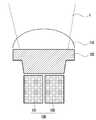
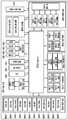
도 1은 본 발명의 다양한 실시예들에 따른 이미지 센서의 개략적인 구조를 도시한 도면이다.1 is a diagram showing a schematic structure of an image sensor according to various embodiments of the present invention.
본 발명의 일 실시예에 따른, 이미지 센서는 마이크로 렌즈(micro lens) (110), 컬러 필터(color filter) (120) 및 복수의 포토다이오드(photodiode) (130)를 포함할 수 있다.An image sensor may include a
마이크로 렌즈(110)는 외부의 빛(L)을 모아서 컬러 필터(120)에 전달할 수 있다. 예를 들어, 마이크로 렌즈(110)는 다양한 입사각에 따라 수신되는 빛(L)을 모아서 컬러 필터(120) 및 포토다이오드(130)로 전달할 수 있다. 일 실시예에 따르면, 마이크로 렌즈(110)는 하단에 배치된 컬러 필터(120) 및 복수의 포토다이오드(130)보다 넓은 면적으로 형성될 수 있다.The
컬러 필터(120)는 수신된 빛(L) 중에서 특정 파장을 가지는 빛을 분리하여 포토다이오드(130)로 전달할 수 있다. 예를 들어, 컬러 필터(120)는 수신된 빛(L) 중에서 적어도 하나 이상의 파장에 대응하는 빛을 분리하여 포토다이오드(130)로 전달할 수 있다. 예를 들어, 컬러 필터(120)는 R(red), G(green), B(blue) 필터들이 일정한 패턴을 가지고 배치된 형태일 수 있다. 예를 들어, R 필터는 수신된 빛(L) 중에서 빨간색의 빛에 대응하는 파장의 빛만을 분리하여 포토다이오드(130)로 전달할 수 있다. G 필터는 수신된 빛(L) 중에서 녹색의 빛에 대응하는 파장의 빛만을 분리하여 포토다이오드(130)로 전달할 수 있다. B 필터는 수신된 빛(L) 중에서 파란색의 빛에 대응하는 파장의 빛만을 분리하여 포토다이오드(130)로 전달할 수 있다. 이 외에 다양한 색의 필터로도 구성이 가능하다. 예를 들자면 RGWB(Red, Green, White, Blue), CYM (Cyan, Yellow, Magenta), 이외에 파장 대역을 3원색이나 보색에 따라 나누지 않고 좁게 나누어 여러 색의 필터를 사용하는 것도 가능하다. 그리고 필터를 사용하지 않고, 실리콘 재질의 빛의 흡수 특성을 이용하여 파장별로 분리하여 사용할 수 있다.The
일 실시예에 따르면, 이미지 센서는 복수의 포토다이오드(131, 133)를 포함할 수 있다. 복수의 포토다이오드(131, 133)는 컬러 필터(120) 하단에 일정한 배열로 배치될 수 있다. 일 실시예에 따르면, 컬러 필터(120) 하단에는 복수의 포토 다이오드가 격자 형태로 배열될 수 있다. 예를 들어, 컬러 필터(120) 하단에는 4개의 포토 다이오드가 2 X 2 배열로 배치될 수 있다. 다양한 실시예들에 따르면, 복수의 포토다이오드(131, 133)는 다양한 배열 및 패턴으로 배치될 수 있다. 포토다이오드(130)는 빛(L)을 전기적 신호로 변환하여 출력할 수 있다.According to one embodiment, the image sensor may include a plurality of
일 실시예에 따르면, 이미지 센서는 빛샘을 방지하고, 이미지 센서로 들어온 빛(L)을 정해진 경로로 유도하는 광 가이드(light guide)(미도시), 포토다이오드(130)가 변환한 전기적 신호(예를 들어, 전기적 에너지)를 저장하는 플로팅 디퓨젼(floating diffusion) 영역(미도시), 이미지 센서에서 처리된 전기적 신호를 출력하는 소스 팔로워(source follower), 포토다이오드(130)가 변환한 전기적 신호를 디지털 신호로 변환하는 컨버터(예를 들어, analog-to-digital convertor, ADC) 및 이미지 센서 내의 신호들을 제어하기 위한 트랜지스터(예를 들어, 트랜스퍼 게이트(transfer gate)를 포함할 수 있다. 본 발명의 다양한 실시예에 따르면, 도 1에 도시하지는 않았으나, 이미지 센서는 포토다이오드(130)를 구동 및 제어하기 위한 회로 구조 및 배선 구조(배선 층)를 포함할 수 있다. 일 실시예에 따르면, 이미지 센서는 포토다이오드(130)로부터 출력되는 신호를 처리하기 위한 프로세서(예를 들어, 디지털 신호 처리 장치(digital signal processor, DSP) 또는, 이미지 처리 장치(image signal processor, ISP) 등)를 포함하거나, 또는, 신호를 처리하기 위한 프로세서와 전기적으로 연결될 수 있다. 본 발명의 다양한 실시예들에 따르면, 이미지 센서는 널리 알려진 CMOS 이미지 센서의 구성 요소들을 더 포함할 수 있다.According to one embodiment, the image sensor includes a light guide (not shown) that prevents light leakage and guides the light L that enters the image sensor to a predetermined path, an electrical signal (not shown) converted by the photodiode 130 A source follower for outputting an electrical signal processed by the image sensor, an electrical signal converted by the
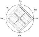
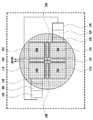
도 2a 및 도 2b는 본 발명의 다양한 실시예들에 따른 이미지 센서의 개략적인 구조를 도시한 평면도이다. 예를 들어, 도 2a 및 도 2b는 도 1에 도시된 이미지 센서를 위에서 내려다본 구조를 도시한다.2A and 2B are plan views illustrating a schematic structure of an image sensor according to various embodiments of the present invention. For example, FIGS. 2A and 2B illustrate a top view of the image sensor shown in FIG.
도 2a를 참조하면, 본 발명의 일 실시예들에 따라, 원형의 마이크로 렌즈(210) 하단에는 사각형 형태의 컬러 필터(220)가 배치되고, 컬러 필터(220) 하단에는 복수의 포토다이오드(231a, 233a, 235a, 237a)가 배치될 수 있다. 일 실시예에 따르면, 복수의 포토다이오드(231a, 233a, 235a, 237a)는 일정한 배열로 배치될 수 있다. 본 발명의 다양한 실시예들에 따르면, 이미지 센서의 구성 및 목적에 따라, 컬러 필터(220)의 모양과 포토다이오드(231a, 233a, 235a, 237a)의 모양은 변경될 수 있다. 예를 들어, 컬러 필터(220) 또는 포토다이오드((231a, 233a, 235a, 237a)는 사각형 이외에도 원형, 육각형 또는 팔각형 등 다양한 형태를 가질 수 있다.2A, a rectangular shaped
일 실시예에 따르면, 복수의 포토다이오드(231a, 233a, 235a, 237a)는 상단, 좌, 우, 하단에 마름모꼴의 형태로 배치될 수 있다. 일 실시예에 따르면, 이미지 센서는 상단의 포토 다이오드(231a) 및 하단의 포토다이오드(237a)로부터 출력되는 신호를 비교할 수 있다. 예를 들어, 이미지 센서는 상단의 포토다이오드(231a) 및 하단의 포토다이오드(237a)로부터 출력되는 신호의 위상차를 비교 및 처리하여 자동 초점 기능을 제공할 수 있다. 이미지 센서는 좌측 포토다이오드(235a) 및 우측 포토다이오드(233a)로부터 출력되는 신호의 위상차를 비교 및 처리하여 자동 초점 기능을 제공할 수 있다.According to one embodiment, the plurality of
도 2b를 참조하면, 복수의 포토다이오드(231b, 233b, 235b, 237b)는 2X2 배열로 상단에 두 개, 하단에 두 개의 형태로 배치될 수 있다. 예를 들어, 복수의 포토다이오드(231b, 233b, 235b, 237b)는 격자 형태로 배치될 수 있다. 일 실시예에 따르면, 이미지 센서는 복수의 포토다이오드(231b, 233b, 235b, 237b) 각각으로부터 출력되는 신호를 비교 및 처리할 수 있다. 예를 들어, 이미지 센서는 복수의 포토다이오드(231b, 233b, 235b, 237b) 각각으로부터 출력되는 신호의 위상차를 비교 및 처리하여 자동 초점 기능을 제공할 수 있다. 예를 들어, 이미지 센서는 각 라인(line) 별로 합산된 신호를 비교하여, 좌우 또는 상하 방향의 위상차를 감지할 수 있는 데이터를 제공할 수 있다. 예를 들어, 이미지 센서는 좌상 및 좌우 포토다이오드(231b, 233b), 좌상 및 좌하 포토다이오드(231b, 235b), 우상 및 우하 포토다이오드(233b, 237b) 또는 좌하 및 우하 포토다이오드(235b, 237b)로부터 출력되는 전기적 신호를 합산할 수 있다. 일 실시예에 따르면, 프로세서(예를 들어, 전자 장치의 프로세서 또는 이미지 센서와 전기적으로 연결된 이미지 시그널 프로세서(image signal processor, ISP) 등)는 이미지 센서로부터 출력된, 합산된 신호를 비교 또는 처리하여 좌우 및 상하 위상차에 따른 자동 초점(auto focusing) 기능을 제공할 수 있다.Referring to FIG. 2B, the plurality of
본 발명의 다양한 실시예들에 따르면, 이미지 센서는 4개 이상의 포토다이오드를 포함할 수 있으며, 복수의 포토다이오드는 도 2a 및 도 2b에 도시된 것에 한정되지 않고, 다양한 형태의 배열로 배치될 수 있다. 또한, 본 발명의 다양한 실시예들에 따르면, 이미지 센서는 복수의 포토다이오드의 배치에 따라 다양한 형태의 배선 구조(배선 층)를 포함할 수 있다.According to various embodiments of the present invention, the image sensor may include four or more photodiodes, and the plurality of photodiodes are not limited to those shown in FIGS. 2A and 2B, but may be arranged in various types of arrangements have. Further, according to various embodiments of the present invention, the image sensor may include various types of wiring structures (wiring layers) depending on the arrangement of the plurality of photodiodes.
도 3은 본 발명의 다양한 실시예들에 따른 이미지 센서의 단위 화소의 구조를 나타낸 도면이다. 도 3은 본 발명의 다양한 실시예에 따라, 복수 개의 포토다이오드들 각각으로부터 신호를 출력하는 경우를 나타낸다.3 is a diagram illustrating a structure of a unit pixel of an image sensor according to various embodiments of the present invention. 3 shows a case of outputting a signal from each of a plurality of photodiodes according to various embodiments of the present invention.
일 실시예에 따르면, 이미지 센서는 복수의 화소를 포함할 수 있다. 예를 들어, 이미지 센서는 복수의 화소들로 구성된 화소 어레이를 포함할 수 있다.According to one embodiment, the image sensor may comprise a plurality of pixels. For example, the image sensor may include a pixel array comprised of a plurality of pixels.
일 실시예에 따르면, 이미지 센서의 복수의 화소 각각(예를 들어, 단위 화소(300))은 빛은 전기적 신호로 변환하는 제1 내지 제4 포토다이오드(311, 313, 315, 317) 및 상기 제1 내지 제4 포토다이오드(311, 313, 315, 317) 각각이 변환한 전기적 신호를 단위 화소(300) 외부로 출력하는 전기적 회로를 포함할 수 있다.According to one embodiment, each of the plurality of pixels (e.g., the unit pixel 300) of the image sensor includes first to
일 실시예에 따르면, 제1 내지 제4 포토다이오드(311, 313, 315, 317)는 일정한 배열로 배치될 수 있다. 예를 들어, 제1 내지 제4 포토다이오드(311, 313, 315, 317)는 단위 화소(300)의 중앙 부분에 배치될 수 있다. 예를 들어, 제1 포토다이오드(311)는 좌측 상단에 배치되고, 제2 포토다이오드(313)는 우측 상단에 배치되고, 제3 포토다이오드(315)는 좌측 하단에 배치되고, 제4 포토다이오드(317)는 우측 하단에 격자 형태로 배치될 수 있다.According to one embodiment, the first to
일 실시예에 따르면, 4개의 포토다이오드들(311, 313, 315, 317)은 각각 개별적으로 동작할 수 있다. 예를 들어, 4개의 포토다이오드들(311, 313, 315, 317)은 각각 또는 적어도 일부는 전기적으로 분리되어 배치될 수 있다. 예를 들어, 제1 포토다이오드(311)와 제2 포토다이오드(313)는 서로 전기적으로 분리되어 배치될 수 있다. 예를 들어, 제3 포토다이오드(315)와 제4 포토다이오드(317)는 서로 전기적으로 분리되어 배치될 수 있다.According to one embodiment, the four
일 실시예에 따르면, 상기 전기적 회로는 상기 제1 내지 제4 포토다이오드(311, 313, 315, 317)가 변환한 전기적 신호를 단위 화소(300) 외부로 출력하는 복수의 플로팅 디퓨젼(floating diffusion) 영역(331, 333, 335, 337) 및 상기 제1 내지 제4 포토다이오드(311, 313, 315, 317)와 상기 복수 개의 플로팅 디퓨젼 영역(331, 333, 335, 337)의 전기적 연결을 온-오프(on-off)하는 복수의 트랜스퍼 게이트(transfer gate)(321, 323, 325, 327)를 포함할 수 있다.According to one embodiment, the electrical circuit includes a plurality of floating diffusion circuits (not shown) for outputting electrical signals converted by the first to
일 실시예에 따르면, 복수의 플로팅 디퓨젼 영역(331, 333, 335, 337)은 제1 포토다이오드(311)가 변환한 전기적 신호를 저장 또는 출력하는 제1 플로팅 디퓨젼 영역(331), 제2 포토다이오드(313)가 변환한 전기적 신호를 저장 또는 출력하는 제2 플로팅 디퓨젼 영역(333), 제3 포토다이오드(315)가 변환한 전기적 신호를 저장 또는 출력하는 제3 플로팅 디퓨젼 영역(335) 및 제4 포토다이오드(317)가 변환한 전기적 신호를 저장 또는 출력하는 제4 플로팅 디퓨젼 영역(337)을 포함할 수 있다.According to one embodiment, the plurality of floating
일 실시예에 따르면, 복수의 포토다이오드(311, 313, 315, 317) 각각의 일 단에는 트랜스퍼 게이트(transfer gate)가 연결될 수 있다. 예를 들어, 제1 포토다이오드(311)와 제1 플로팅 디퓨전 영역(331) 사이에는 제1 트랜스퍼 게이트(321)가 연결되고, 제2 포토다이오드(313)와 제2 플로팅 디퓨젼 영역(333) 사이에는 제2 트랜스퍼 게이트(323)가 연결되고, 제3 포토다이오드(315)와 제3 플로팅 디퓨젼 영역(335) 사이에는 제3 트랜스퍼 게이트(325)가 연결되고, 제4 포토다이오드(317)와 제4 플로팅 디퓨젼 영역(337) 사이에는 제4 트랜스퍼 게이트(327)가 연결될 수 있다. 상기 제1 내지 제4 트랜스퍼 게이트(321, 323, 325, 327)는 연결된 제1 내지 제4 포토다이오드(311, 313, 315, 317) 각각이 변환한 전기적 신호를 대응되는 제1 내지 제4 플로팅 디퓨젼 영역(331, 333, 335, 337)으로 전송하는 것을 제어할 수 있다. 예를 들어, 제1 트랜스퍼 게이트(321)는, 제1 포토다이오드(311)와 제1 플로팅 디퓨젼 영역(331)의 전기적 연결을 온-오프(on-off)제어함으로써, 제1 포토다이오드(311)에서 변환한 전기적 신호를 제1 플로팅 디퓨젼 영역(331)으로 전달시키거나, 전기적 신호의 전달을 방지할 수 있다.According to one embodiment, a transfer gate may be connected to one end of each of the plurality of
일 실시예에 따르면, 복수의 플로팅 디퓨젼 영역(331, 333, 335, 337) 각각의 일 단에는 전기적 신호를 화소(300) 외부로 출력하는 소스 팔로워(source follower)가 연결될 수 있다. 예를 들어, 제1 플로팅 디퓨젼 영역(331)의 일 단에는 제1 소스 팔로워(341)가 연결되고, 제2 플로팅 디퓨젼 영역(333)의 일 단에는 제2 소스 팔로워(343)가 연결되고, 제3 플로팅 디퓨젼 영역(335)의 일 단에는 제3 소스 팔로워(345)가 연결되고, 제4 플로팅 디퓨젼 영역(337)의 일 단에는 제4 소스 팔로워(347)가 연결될 수 있다. 일 실시예에 따르면, 복수의 소스 팔로워(341, 343, 345, 347) 각각은 대응되는 플로팅 디퓨젼 영역에 저장된 전기적 에너지(예를 들어, 복수의 포토다이오드(311, 313, 315, 317) 각각이 빛을 변환하여 생성한 전기적 에너지)에 대응되는 전기적 신호를 화소(300) 외부로 출력할 수 있다.According to one embodiment, a source follower may be connected to one end of each of the plurality of floating
일 실시예에 따르면, 일 실시예에 따르면, 프로세서(예를 들어, 전자 장치의 프로세서 또는 이미지 센서와 전기적으로 연결된 이미지 시그널 프로세서(image signal processor, ISP) 등)는 복수 개의 포토다이오드(311, 313, 315, 317) 각각으로부터 출력되는 신호를 이용하여 자동 초점(auto focusing) 기능을 제공할 수 있다. 예를 들어, 도 12에 도시된 전자 장치의 프로세서(1210) 또는, 카메라 모듈(1291)에 포함된 이미지 시그널 프로세서(ISP)는 복수의 포토다이오드(311, 313, 315, 317) 각각으로부터 출력되는 신호를 이용하여 자동 초점(auto focusing) 기능을 제공할 수 있다.According to one embodiment, a processor (e.g., an image signal processor (ISP), etc., electrically coupled to a processor of an electronic device or an image sensor) may include a plurality of photodiodes 311,313 , 315, and 317 may be used to provide an auto focusing function. For example, the processor 1210 of the electronic device shown in FIG. 12 or the image signal processor ISP included in the
예를 들어, 프로세서(예를 들어, 전자 장치의 프로세서 또는 이미지 센서와 전기적으로 연결된 이미지 시그널 프로세서(image signal processor, ISP) 등)는 단위 화소(300)에서 출력되는 신호를 비교 및 처리할 수 있다. 예를 들어, 프로세서(예를 들어, 전자 장치의 프로세서 또는 이미지 센서와 전기적으로 연결된 이미지 시그널 프로세서(image signal processor, ISP) 등)는 단위 화소(300)에서 출력되는 신호를 이용하여 영상의 위상차를 검출할 수 있다. 예를 들어, 이미지 센서는 단위 화소(300)에서 출력되는 신호를 합산할 수 있다. 예를 들어, 프로세서(예를 들어, 전자 장치의 프로세서 또는 이미지 센서와 전기적으로 연결된 이미지 시그널 프로세서(image signal processor, ISP) 등)는 단위 화소(300)에서 출력되는 신호를 합산 및 처리하여 자동 초점 기능을 수행할 수 있다. 예를 들어, 프로세서(예를 들어, 전자 장치의 프로세서 또는 이미지 센서와 전기적으로 연결된 이미지 시그널 프로세서(image signal processor, ISP) 등)는 좌측의 포토다이오드(311, 315) 및 우측의 포토다이오드(313, 317)로부터 출력되는 전기적 신호를 이용하여 이미지의 좌우 방향의 초점을 조정할 수 있다. 예를 들어, 프로세서(예를 들어, 전자 장치의 프로세서 또는 이미지 센서와 전기적으로 연결된 이미지 시그널 프로세서(image signal processor, ISP) 등)는 상단의 포토다이오드(311, 313) 및 하단의 포토다이오드(315, 317)로부터 출력되는 전기적 신호를 이용하여 이미지의 상하 방향의 초점을 조정할 수 있다.For example, a processor (e.g., a processor of an electronic device or an image signal processor (ISP) electrically coupled to an image sensor, etc.) may compare and process signals output from the
다양한 실시예들에 따르면, 이미지 센서는 1회에 제1 내지 제4 포토다이오드(311,313, 315, 317)가 변환하는 모든 신호를 출력 받아 처리하거나, 2회 또는 4회로 나누어 처리할 수 있다. 예를 들어, 이미지 센서는 단위 화소(300) 내의 제1 내지 제4 포토다이오드(341, 343, 345, 347)가 변환한 신호를 한 번에 모두 출력하도록 제어할 수 있다. 또는, 이미지 센서는 제1 내지 제4 포토다이오드(341, 343, 345, 347)가 라인(line) 별로 신호를 출력하도록 제어할 수 있다. 예를 들어, 이미지 센서는 상단의 포토다이오드(311, 313)으로부터 출력되는 신호를 먼저 처리하고, 하단의 포토다이오드(315, 317)로부터 출력되는 신호를 처리할 수 있다. 또는, 이미지 센서는 복수의 포토다이오드(341, 343, 345, 347) 각각이 순차적으로 4회에 걸쳐 출력되는 신호를 처리할 수 있다.According to various embodiments, the image sensor may process all the signals converted by the first through
예를 들어, 이미지 센서가 복수의 포토다이오드(341, 343, 345, 347)로부터 출력되는 모든 신호를 한 번에 처리하는 경우, 프로세서가 더 빠른 속도로 모든 신호를 얻을 수 있으나, 1회에 처리할 화소 수가 증가하여 처리 회로의 구성이 더 복잡해지고, 필요한 회로가 증가할 수 있다. 또한, 한 번에 전송하는 전송 신호가 증가하여 전송 선로의 부하가 커지고, 프로세서가 처리해야 할 연산량(예를 들어, 프로세서가 각 신호들을 비교 및 가산하는 연산 횟수 등)이 증가하여 프레임 율(frame rate)이 저하될 수 있다. 반면에, 모든 포토다이오드(341, 343, 345, 347)로부터 하나씩 순차적으로 신호를 출력하도록 하는 경우, 신호를 획득하는 속도가 저하될 수 있다. 예를 들어, 이미지 센서가 네 개의 포토다이오드(341, 343, 345, 347) 중 두 개씩의 포토다이오드들로부터 출력되는 신호를 처리할 경우, 처리 속도, 전송 부하, 및 프로세서의 연산량을 종합적으로 고려할 때 가장 효율적인 이미지 처리가 가능할 수 있다. 본 발명의 다양한 실시예들에 따르면, 이미지 센서는 다양한 상황 또는 원하는 조건에 따라 단위 화소에 포함된 복수의 포토다이오드(341, 343, 345, 347)들을 제어하여 상기 모든 방식을 사용할 수 있다.For example, if the image sensor processes all of the signals output from the plurality of
도 4는 본 발명의 다양한 실시예들에 따른 이미지 센서의 단위 화소의 구조를 나타낸 도면이다. 이하에서는, 상기 도 3에서 설명한 이미지 센서의 단위 화소의 구성과 구별되는 특징을 중점적으로 설명한다.4 is a diagram illustrating the structure of a unit pixel of an image sensor according to various embodiments of the present invention. Hereinafter, the features different from the configuration of the unit pixel of the image sensor described with reference to FIG. 3 will be mainly described.
일 실시예예 따르면, 이미지 센서의 복수의 화소 각각은 제1 내지 제4 포토다이오드(411, 413, 415, 417), 복수의 트랜스퍼 게이트(421, 423, 425, 427), 복수의 플로팅 디퓨젼 영역(431, 433), 및 복수의 소스 팔로워(441, 443)를 포함할 수 있다.According to one embodiment, each of the plurality of pixels of the image sensor includes first to
일 실시예에 따르면, 4개의 포토다이오드들(411, 413, 415, 417)의 각각 또는 적어도 일부는 전기적으로 분리되어 배치될 수 있다. 예를 들어, 제1 포토다이오드(411)와 제2 포토다이오드(413)는 서로 전기적으로 분리되어 배치될 수 있다. 예를 들어, 제3 포토다이오드(415)와 제4 포토다이오드(415)는 서로 전기적으로 분리되어 배치될 수 있다.According to one embodiment, each or at least a portion of the four
일 실시예에 따르면, 단위 화소(400)는 제1 포토다이오드(411) 또는 제3 포토다이오드(415)가 변환한 전기적 신호를 단위 화소(400) 외부로 출력하는 제1 플로팅 디퓨젼 영역(431) 및 제2 포토다이오드(413) 또는 제4 포토다이오드(415)가 변환한 전기적 신호를 단위 화소(400) 외부로 출력하는 제2 플로팅 디퓨젼 영역(433)을 포함할 수 있다.The
일 실시예에 따르면, 복수의 포토다이오드(411, 413, 415, 417) 각각의 일 단에는 트랜스퍼 게이트(transfer gate)가 연결될 수 있다. 예를 들어, 제1 포토다이오드(411)와 제1 플로팅 디퓨전 영역 사이에는 제1 트랜스퍼 게이트(421)가 연결되고, 제2 포토다이오드(413)와 제2 플로팅 디퓨젼 영역(433) 사이에는 제2 트랜스퍼 게이트(423)가 연결되고, 제3 포토다이오드(415)와 제1 플로팅 디퓨젼 영역(431) 사이에는 제3 트랜스퍼 게이트(425)가 연결되고, 제4 포토다이오드(415)와 제2 플로팅 디퓨젼 영역(433) 사이에는 제4 트랜스퍼 게이트(427)가 연결될 수 있다.According to one embodiment, a transfer gate may be connected to one end of each of the plurality of
일 실시예에 따르면, 제1 플로팅 디퓨젼 영역(431)의 일 단에는 제1 소스 팔로워(441)가 연결되고, 제2 플로팅 디퓨젼 영역(433)의 일 단에는 제2 소스 팔로워(443)가 연결될 수 있다.According to one embodiment, a
일 실시예에 따르면, 이미지 센서의 단위 화소(400)는 복수의 포토다이오드(411, 413, 415, 417)들 중에서 적어도 두 개의 포토다이오드가 플로팅 디퓨젼 영역 및 소스 팔로워를 공유할 수 있다.According to one embodiment, the
예를 들어, 제1 포토다이오드(411) 또는 제3 포토다이오드(415)가 변환한 전기적 신호는 제1 플로팅 디퓨젼 영역(431)에 저장(또는, 축적)되거나, 또는 제1 플로팅 디퓨젼 영역(431) 및 제1 소스 팔로워(441)를 통하여 단위 화소(400) 외부로 출력될 수 있다. 제2 포토다이오드(413) 또는 제4 포토다이오드(415)가 변환한 전기적 신호는 제2 플로팅 디퓨젼 영역(433)에 저장되거나, 또는 제2 플로팅 디퓨젼 영역(433) 및 제2 소스 팔로워(443)를 통하여 단위 화소(400) 외부로 출력될 수 있다.For example, the electrical signals converted by the
일 실시예에 따르면, 이미지 센서는 복수의 트랜스퍼 게이트(421, 423, 425, 427)를 제어하여, 복수의 포토다이오드(411, 413, 415, 417)가 변환한 전기적 신호를 라인 별로 처리할 수 있다. 예를 들어, 제1 트랜스퍼 게이트(421) 및 제2 트랜스퍼 게이트(423)는 동일한 제어 신호에 따라 제어되도록 전기적으로 연결되고, 제3 트랜스퍼 게이트(425) 및 상기 제4 트랜스퍼 게이트(427)는, 상기 제1 및 제2 트랜스퍼 게이트(423)의 제어 신호와는 다른, 동일한 제어 신호에 따라 제어되도록 전기적으로 연결될 수 있다.According to one embodiment, the image sensor controls a plurality of
일 실시예에 따르면, 이미지 센서는 제1 트랜스퍼 게이트(421)가 제1 포토다이오드(411)와 제1 플로팅 디퓨젼 영역(431)을 전기적으로 연결시킴과 동시에 제2 트랜스퍼 게이트(423)가 제2 포토다이오드(413)와 제2 플로팅 디퓨젼 영역(433)을 전기적으로 연결시키도록 제어할 수 있다. 또한, 이미지 센서는 제3 트랜스퍼 게이트(425) 및 제4 트랜스퍼 게이트(427)는 제3 포토다이오드(415) 및 제4 포토다이오드(415)는 제1 플로팅 디퓨젼 영역(431) 및 제2 플로팅 디퓨젼 영역(433)과 전기적으로 차단되게 함으로써, 상단의 제1 포토다이오드(411) 및 제2 포토다이오드(413)가 변환한 신호만이 단위 화소(400) 외부로 출력되도록 할 수 있다. 예를 들어, 제1 포토다이오드(411)가 변환한 전기적 신호가 제1 플로팅 디퓨젼 영역(431) 및 제1 소스 팔로워(441)를 통하여 출력되고, 제2 포토다이오드(413)가 변환한 전기적 신호가 제2 플로팅 디퓨젼 영역(433) 및 제2 소스 팔로워(443)를 통하여 출력될 수 있다.The
동일한 방식으로, 이미지 센서는 제1 트랜스퍼 게이트(421) 및 제2 트랜스퍼 게이트(423)는 차단시키고, 제3 트랜스퍼 게이트(425) 및 제4 프랜스퍼 게이트를 연결시킴으로써, 하단의 제3 포토다이오드(415) 및 제4 포토다이오드(415)가 변환한 신호만이 단위 화소(400) 외부로 출력되도록 할 수 있다. 예를 들어, 제3 포토다이오드(415)가 변환한 전기적 신호가 제1 플로팅 디퓨젼 영역(431) 및 제1 소스 팔로워(441)를 통하여 출력되고, 제4 포토다이오드(415)가 변환한 전기적 신호가 제2 플로팅 디퓨젼 영역(433) 및 제2 소스 팔로워(443)를 통하여 출력될 수 있다.In the same manner, the image sensor blocks the
다양한 실시예들에 따르면, 이미지 센서는 복수의 트랜스퍼 게이트(421, 423, 425, 427)를 제어하여 단위 화소(400) 내의 복수의 포토다이오드(411, 413, 415, 417)들이 변환한 전기적 신호를 라인 별로 획득 및 처리할 수 있다.According to various embodiments, the image sensor may control a plurality of
도 5는 본 발명의 다양한 실시예들에 따른 이미지 센서의 단위 화소의 회로도이다. 도 5는 도 4에 도시된 단위 화소의 회로를 개략적으로 도시한 도면이다.5 is a circuit diagram of a unit pixel of an image sensor according to various embodiments of the present invention. 5 is a view schematically showing a circuit of the unit pixel shown in Fig.
일 실시예에 따르면, 복수의 포토다이오드(PD1, PD2, PD3, PD4) 중에서 적어도 일부는 전기적으로 분리되어 배치될 수 있다. 예를 들어, 제1 포토다이오드(PD1)와 제3 포토다이오드(PD3)가 포함된 좌측 회로와 제2 포토다이오드(PD2)와 제4 포토다이오드(PD4)가 포함된 우측 회로는 전기적으로 분리될 수 있다.According to one embodiment, at least some of the plurality of photodiodes (PD1, PD2, PD3, PD4) may be disposed electrically separated. For example, the left circuit including the first photodiode PD1 and the third photodiode PD3, and the right circuit including the second photodiode PD2 and the fourth photodiode PD4 are electrically disconnected .
일 실시예에 따르면, 복수의 포토다이오드(PD1, PD2, PD3, PD4) 각각의 일 단에는 대응되는 복수의 트랜스퍼 게이트 각각이 연결될 수 있다. 예를 들어, 제1 포토다이오드(PD1)의 일 단에는 제1 트랜스퍼 게이트(TG1)가 연결되고, 제3 포토다이오드(PD3)의 일 단에는 제3 트랜스퍼 게이트(TG3)가 연결될 수 있다. 제1 트랜스퍼 게이트(TG1)와 제3 트랜스퍼 게이트(TG3)의 일 단은 서로 연결될 수 있다. 예를 들어, 제1 포토다이오드(PD1) 및 제1 트랜스퍼 게이트(TG1)와 제3 포토다이오드(PD3) 및 제3 트랜스퍼 게이트(TG3)는 서로 병렬로 연결될 수 있다.According to one embodiment, each of the plurality of photodiodes PD1, PD2, PD3, and PD4 may have a plurality of corresponding transfer gates connected to one end thereof. For example, the first transfer gate TG1 may be connected to one end of the first photodiode PD1, and the third transfer gate TG3 may be connected to one end of the third photodiode PD3. One end of the first transfer gate TG1 and one end of the third transfer gate TG3 may be connected to each other. For example, the first photodiode PD1 and the first transfer gate TG1, the third photodiode PD3, and the third transfer gate TG3 may be connected in parallel with each other.
제1 트랜스퍼 게이트(TG1)와 제3 트랜스퍼 게이트(TG3)가 연결된 단에는 제1 플로팅 디퓨젼 영역(CFD1)이 연결될 수 있다. 예를 들어, 제1 트랜스퍼 게이트(TG1)와 제3 트랜스퍼 게이트(TG3)가 연결된 단에는 제1 포토다이오드(PD1) 또는 제3 포토다이오드(PD3)가 변환한 전기적 에너지(전기적 신호)를 저장하기 위한 제1 플로팅 디퓨젼 캐패시터(CFD1)가 연결될 수 있다.A first floating diffusion region CFD1 may be connected to an end connected to the first transfer gate TG1 and the third transfer gate TG3. For example, the first photodiode PD1 or the third photodiode PD3 stores the converted electrical energy (electrical signal) at an end connected to the first transfer gate TG1 and the third transfer gate TG3 A first floating diffusion capacitor CFD1 may be connected.
제1 플로팅 디퓨젼 영역(CFD1)에는 제1 소스 팔로워(541)가 연결될 수 있다. 제1 소스 팔로워(541)의 일 단에는 전원(VDD)이 연결될 수 있다. 제1 소스 팔로워(541)를 제어하기 위한 입력단(예를 들어, 제1 소스 팔로워(541)의 트랜지스터의 게이트 단)은 제1 트랜스퍼 게이트(TG1), 제3 트랜스퍼 게이트(TG3), 및 제1 플로팅 디퓨젼 영역(CFD1)이 연결된 단과 연결될 수 있다. 제1 소스 팔로워(541)는 제1 플로팅 디퓨젼 영역(CFD1)에 저장된 전기적 에너지(전기적 신호)를 단위 화소 외부로 출력할 수 있다. 즉, 제1 소스 팔로워(541)는 제1 출력 신호(OUT1)를 출력할 수 있다. 일 실시예에 따르면, 제1 소스 팔로워(541)는 출력 신호를 선택하기 위한 제1 선택 소자(S1)를 포함할 수 있다. 예를 들어, 제1 소스 팔로워(541)는 제1 선택 소자(S1)에 신호 출력을 위한 신호가 입력되는 경우에 제1 출력 신호(OUT1)를 출력할 수 있다.A
일 실시예에 따르면, 상기 제1 소스 팔로워(541)를 제어하기 위한 입력단과 전원(VDD) 사이에는 제1 리셋 소자(R1)가 연결될 수 있다. 예를 들어, 이미지 센서는 제1 리셋 소자(R1)를 제어하여, 제1 플로팅 디퓨젼 영역(CFD1)에 전기적 에너지(전기적 신호)가 저장되기 전과 후에 회로를 리셋시켜서 오차를 줄이고, 더 정확한 자동 포커싱 기능을 제공할 수 있다.According to one embodiment, a first reset element Rl may be connected between an input terminal for controlling the
일 실시예에 따르면, 제2 포토다이오드(PD2)의 일 단에는 제2 트랜스퍼 게이트(TG2)가 연결되고, 제4 포토다이오드(PD4)의 일 단에는 제4 트랜스퍼 게이트(TG4)가 연결될 수 있다. 제2 트랜스퍼 게이트(TG2)와 제4 트랜스퍼 게이트(TG4)의 일 단은 서로 연결될 수 있다. 예를 들어, 제2 포토다이오드(PD2) 및 제2 트랜스퍼 게이트(TG2)와 제4 포토다이오드(PD4) 및 제4 트랜스퍼 게이트(TG4)는 서로 병렬로 연결될 수 있다.According to one embodiment, a second transfer gate TG2 may be connected to one end of the second photodiode PD2, and a fourth transfer gate TG4 may be connected to one end of the fourth photodiode PD4 . One end of the second transfer gate TG2 and one end of the fourth transfer gate TG4 may be connected to each other. For example, the second photodiode PD2 and the second transfer gate TG2, the fourth photodiode PD4, and the fourth transfer gate TG4 may be connected in parallel with each other.
제2 트랜스퍼 게이트(TG2)와 제4 트랜스퍼 게이트(TG4)가 연결된 단에는 제2 플로팅 디퓨젼 영역(CFD2)이 연결될 수 있다. 예를 들어, 제2 트랜스퍼 게이트(TG2)와 제4 트랜스퍼 게이트(TG4)가 연결된 단에는 제2 포토다이오드(PD2) 또는 제4 포토다이오드(PD4)가 변환한 전기적 에너지(전기적 신호)를 저장하기 위한 제2 플로팅 디퓨젼 캐패시터(CFD2)가 연결될 수 있다.And a second floating diffusion region CFD2 may be connected to an end to which the second transfer gate TG2 and the fourth transfer gate TG4 are connected. For example, the second photodiode PD2 or the fourth photodiode PD4 stores the converted electrical energy (electrical signal) at an end connected to the second transfer gate TG2 and the fourth transfer gate TG4 A second floating diffusion capacitor CFD2 may be connected.
제2 플로팅 디퓨젼 영역(CFD2)에는 제2 소스 팔로워(543)가 연결될 수 있다. 제2 소스 팔로워(543)의 일 단에는 전원(VDD)이 연결될 수 있다. 제2 소스 팔로워(543)를 제어하기 위한 입력단(예를 들어, 제2 소스 팔로워(543)의 트랜지스터의 게이트 단)은 제2 트랜스퍼 게이트(TG2), 제4 트랜스퍼 게이트(TG4), 및 제2 플로팅 디퓨젼 영역(CFD2)이 연결된 단과 연결될 수 있다. 제2 소스 팔로워(543)는 제2 플로팅 디퓨젼 영역(CFD2)에 저장된 전기적 에너지(전기적 신호)를 단위 화소 외부로 출력할 수 있다. 즉, 제2 소스 팔로워(543)는 제2 출력 신호(OUT2)를 출력할 수 있다. 일 실시예에 따르면, 제2 소스 팔로워(543)는 출력 신호를 선택하기 위한 제2 선택 소자(S2)를 포함할 수 있다. 예를 들어, 제2 소스 팔로워(543)는 제2 선택 소자(S2)에 신호 출력을 위한 신호가 입력되는 경우에 제2 출력 신호(OUT2)를 출력할 수 있다.A
일 실시예에 따르면, 상기 제2 소스 팔로워(543)를 제어하기 위한 입력단과 전원(VDD) 사이에는 제2 리셋 소자(R2)가 연결될 수 있다. 예를 들어, 이미지 센서는 제2 리셋 소자(R2)를 제어하여, 제2 플로팅 디퓨젼 영역(CFD2)에 전기적 에너지(전기적 신호)가 저장되기 전과 후에 회로를 리셋시켜서 오차를 줄이고, 더 깨끗한 이미지를 제공할 수 있다.According to one embodiment, a second
도 6은 본 발명의 다양한 실시예들에 따른 이미지 센서의 단위 화소의 구조를 나타낸 도면이다. 이하에서는, 도 4에서 설명한 이미지 센서의 단위 화소의 구성과 구별되는 특징을 중점적으로 설명한다.6 is a diagram illustrating a structure of a unit pixel of an image sensor according to various embodiments of the present invention. Hereinafter, the features different from the configuration of the unit pixel of the image sensor described with reference to FIG. 4 will be mainly described.
일 실시예에 따르면, 이미지 센서의 단위 화소(600)는 복수의 포토다이오드(611, 613, 615, 617), 복수의 트랜스퍼 게이트(621, 623, 625, 627, 651, 653), 복수의 플로팅 디퓨젼 영역(631, 633) 및 복수의 소스 팔로워(641, 643)를 포함할 수 있다.The
일 실시예에 따르면, 단위 화소(600)는 트랜스퍼 게이트의 제어에 따라, 제1 포토다이오드(611) 내지 제4 포토다이오드(617)가 변환한 전기적 신호를 단위 화소(600) 외부로 출력하는 제1 플로팅 디퓨젼 영역(631) 및 제2 플로팅 디퓨젼 영역(633)을 포함할 수 있다.According to one embodiment, the
일 실시예에 따르면, 복수의 포토다이오드(611, 613, 615, 617) 각각의 양 단에는 트랜스퍼 게이트가 배치될 수 있다. 예를 들어, 제1 포토다이오드(611)와 제1 플로팅 디퓨전 영역(631) 사이에는 제1 트랜스퍼 게이트(621)가 연결되고, 제2 포토다이오드(613)와 제2 플로팅 디퓨젼 영역(633) 사이에는 제2 트랜스퍼 게이트(623)가 연결되고, 제3 포토다이오드(615)와 제1 플로팅 디퓨젼 영역(631) 사이에는 제3 트랜스퍼 게이트(625)가 연결되고, 제4 포토다이오드(617)와 제2 플로팅 디퓨젼 영역(633) 사이에는 제4 트랜스퍼 게이트(627)가 연결될 수 있다. 제1 포토다이오드(611)와 제2 포토다이오드(613) 사이에는 제1 포토다이오드(611)와 제2 포토다이오드(613)의 전기적 연결을 온 오프 제어하는 제5 트랜스퍼 게이트(651)가 연결될 수 있다. 제3 포토다이오드(615)와 제4 포토다이오드(617) 사이에는 제3 포토다이오드(615)와 제4 포토다이오드(617)의 전기적 연결을 온 오프 제어하는 제6 트랜스퍼 게이트(653)가 연결될 수 있다.According to one embodiment, transfer gates may be disposed at both ends of each of the plurality of
일 실시예에 따르면, 상기 제5 트랜스퍼 게이트(651) 및 상기 제6 트랜스퍼 게이트(653)는 동일한 제1 제어 신호에 따라 제어되도록 전기적으로 연결될 수 있다. 상기 제1 트랜스퍼 게이트(621) 및 상기 제4 트랜스퍼 게이트(627)는 동일한 제2 제어 신호에 따라 제어되도록 전기적으로 연결될 수 있다. 상기 제2 트랜스퍼 게이트(623) 및 상기 제3 트랜스퍼 게이트(625)는 동일한 제3 제어 신호에 따라 제어되도록 전기적으로 연결될 수 있다.According to one embodiment, the
일 실시예에 따르면 이미지 센서는, 상기 복수의 트랜스퍼 게이트(621, 623, 625, 627, 651, 653)를 제어함으로써, 단위 화소(600)가 상기 복수의 포토다이오드(611, 613, 615, 617)가 변환한 전기적 신호 중 적어도 두 개를 합산하여 출력하도록 제어할 수 있다.According to one embodiment, the image sensor controls the plurality of
이하, 제1 내지 제3 제어 신호가 대응되는 트랜스퍼 게이트를 온 또는 오프하기 위한 신호라고 가정하여 설명한다.Hereinafter, it is assumed that the first to third control signals are signals for turning on or off the corresponding transfer gate.
예를 들어, 제1 제어 신호가 온, 제2 제어 신호가 온, 제3 제어 신호가 오프 신호인 경우, 제5 트랜스퍼 게이트(651)가 제1 포토다이오드(611) 및 제2 포토다이오드(613)를 전기적으로 연결하여 제1 포토다이오드(611) 및 제2 포토다이오드(613)가 변환한 전기적 신호가 합산될 수 있다. 또한, 제6 트랜스퍼 게이트(653)가 제3 포토다이오드(615) 및 제4 포토다이오드(617)를 전기적으로 연결하여 제3 포토다이오드(615) 및 제4 포토다이오드(617)가 변환한 전기적 신호가 합산될 수 있다. 이 경우, 제2 제어신호에 따라 제1 트랜스퍼 게이트(621)가 제1 플로팅 디퓨젼 영역(631)과 제1 포토다이오드(611)를 전기적으로 연결함에 따라, 상단의 제1 포토다이오드(611) 및 제2 포토다이오드(613)로부터 변환되어 합산된 전기적 신호는 제1 플로팅 디퓨젼 영역(631) 및 제1 소스 팔로워(641)를 통해 화소(600) 외부로 출력될 수 있다. 또한, 제2 제어신호에 따라 제4 트랜스퍼 게이트(627)가 제2 플로팅 디퓨젼 영역(633)과 제4 포토다이오드(617)를 전기적으로 연결함에 따라, 하단의 제3 포토다이오드(615) 및 제4 포토다이오드(617)로부터 변환되어 합산된 전기적 신호는 제2 플로팅 디퓨젼 영역(633) 및 제2 소스 팔로워(643)를 통해 화소(600) 외부로 출력될 수 있다.For example, when the first control signal is ON, the second control signal is ON, and the third control signal is OFF signal, the
예를 들어, 제1 제어 신호가 온 신호, 제2 제어 신호 및 제3 제어 신호 중 하나가 온 신호, 제2 제어 신호 및 제3 제어 신호 중 하나가 오프 신호인 경우에, 상단의 포토다이오드(611, 613)가 변환한 신호들이 합산된 신호와 하단의 포토다이오드(615, 617)가 변환한 신호들이 합산된 신호가 각각 제1 플로팅 디퓨젼 영역(631) 또는 제2 플로팅 디퓨젼 영역(633) 중 하나를 통하여 화소(600) 외부로 출력될 수 있다.For example, when one of the first control signal, the second control signal, and the third control signal is an ON signal, and one of the second control signal and the third control signal is an OFF signal, the
이 경우, 이미지 센서는 상부 및 하부의 합산 신호를 획득할 수 있다. 일 실시예에 따르면, 프로세서(예를 들어, 전자 장치의 프로세서 또는 이미지 센서와 전기적으로 연결된 이미지 시그널 프로세서(image signal processor, ISP) 등)는 상부 포토다이오드(611, 613) 및 하부 포토다이오드들(615, 617)이 변환한 전기적 신호를 비교 및 처리할 수 있다. 예를 들어, 프로세서(예를 들어, 전자 장치의 프로세서 또는 이미지 센서와 전기적으로 연결된 이미지 시그널 프로세서(image signal processor, ISP) 등)는 상단 및 하단의 합산된 전기적 신호들의 위상차를 검출하고, 이를 처리함으로써 상하 방향의 초점을 조정하여 자동 포커싱 기능을 수행할 수 있다.In this case, the image sensor can acquire the summation signals of the upper and lower portions. In accordance with one embodiment, a processor (e.g., an image signal processor (ISP), etc., electrically coupled to a processor or an image sensor of an electronic device) is coupled to the
다른 예로, 제1 제어 신호가 오프, 제2 제어 신호 및 제3 제어 신호가 온인 경우, 제5 트랜스퍼 게이트(651)가 제1 포토다이오드(611) 및 제2 포토다이오드(613)를 전기적으로 분리시키고, 제6 트랜스퍼 게이트(653)가 제3 포토다이오드(615) 및 제4 포토다이오드(617)를 전기적으로 분리시킬 수 있다. 제1 트랜스퍼 게이트(621)는 제1 포토다이오드(611) 및 제1 플로팅 디퓨젼 영역(631)을 전기적으로 연결시키고, 제3 트랜스퍼 게이트(625)는 제3 포토다이오드(615) 및 제1 플로팅 디퓨젼 영역(631)을 전기적으로 연결시킬 수 있다. 제2 트랜스퍼 게이트(623)는 제2 포토다이오드(613) 및 제2 플로팅 디퓨젼 영역(633)을 전기적으로 연결시키고, 제4 트랜스퍼 게이트(627)는 제4 포토다이오드(617) 및 제2 플로팅 디퓨젼 영역(633)을 전기적으로 연결시킬 수 있다. 이 경우, 제1 포토다이오드(611)가 변환한 전기적 신호 및 제3 포토다이오드(615)가 변환한 전기적 신호는 제1 플로팅 디퓨젼 영역(631)에서 합산되고, 제2 포토다이오드(613)가 변환한 전기적 신호 및 제4 포토다이오드(617)가 변환한 전기적 신호는 제2 플로팅 디퓨젼 영역(633)에서 합산될 수 있다. 예를 들어, 좌측 포토다이오드(611, 615)가 변환한 신호들이 합산된 신호와 우측의 포토다이오드(613, 617)가 변환한 신호들이 합산된 신호가 각각 제1 플로팅 디퓨젼 영역(631) 및 제2 플로팅 디퓨젼 영역(633)을 통하여 화소(600) 외부로 출력될 수 있다.As another example, when the first control signal is off, the second control signal and the third control signal are on, the
이 경우, 이미지 센서는 좌측 및 우측의 합산 신호를 획득할 수 있다. 일 실시예에 따르면, 프로세서(예를 들어, 전자 장치의 프로세서 또는 이미지 센서와 전기적으로 연결된 이미지 시그널 프로세서(image signal processor, ISP) 등)는 좌측 포토다이오드(611, 615) 및 우측 포토다이오드들(613, 617)이 변환한 전기적 신호를 비교 및 처리할 수 있다. 예를 들어, 프로세서(예를 들어, 전자 장치의 프로세서 또는 이미지 센서와 전기적으로 연결된 이미지 시그널 프로세서(image signal processor, ISP) 등)는 좌측 및 우측의 합산된 전기적 신호들의 위상차를 검출하고, 이를 처리함으로써 좌우 방향의 초점을 조정하여 자동 포커싱 기능을 수행할 수 있다.In this case, the image sensor can obtain left and right summed signals. According to one embodiment, a processor (e.g., an image signal processor (ISP), etc., electrically coupled to a processor of an electronic device or an image sensor, etc.) is coupled to the
본 발명의 다양한 실시예에 따르면, 이미지 센서는 화소(600) 내의 복수의 포토다이오드(611, 613, 615, 617) 중 적어도 일부의 사이에 제어 가능한 트랜스퍼 게이트를 포함함으로써, 화소(600) 내의 상하 또는 좌우의 포토다이오드들이 변환한 전기적 신호를 합산하여 화소(600) 외부로 출력할 수 있다. 예를 들어, 이미지 센서는 복수의 트랜스퍼 게이트의 제어에 따라, 좌우 또는 상하 방향의 위상차를 모두 검출할 수 있는 신호를 출력할 수 있고, 이에 따라 프로세서(예를 들어, 전자 장치의 프로세서 또는 이미지 센서와 전기적으로 연결된 이미지 시그널 프로세서(image signal processor, ISP) 등)는 사용자에게 좌우 방향 또는 상하 방향 모두에서 더 정확하고 신속한 자동 초점 기능을 제공할 수 있다. 또한, 본 발명의 다양한 실시예에 따른 이미지 센서는 적어도 두 개의 포토다이오드가 변환한 신호를 합산한 신호를 전송함으로써, 전송 부하를 감소시키고, 프로세서의 신호 연산량을 감소시킬 수 있다. 예를 들어, 프로세서는 복수의 트랜스퍼 게이트를 제어함으로써, 원하는 방향의 신호를 바로 획득할 수 있고, 신호의 합산으로 인하여 각각의 신호를 합산하는 연산 없이 바로 좌우 또는 상하 방향의 위상차를 연산할 수 있다. 본 발명의 다양한 실시예들에 따른 이미지 센서는, 프로세서의 연산량을 감소시키고, 상하 및 좌우 방향 모두의 신호를 획득함으로써, 사용자에게 보다 정확하고 신속한 자동 초점 기능을 제공할 수 있다.According to various embodiments of the present invention, the image sensor includes a controllable transfer gate between at least some of the plurality of
도 7은 본 발명의 다양한 실시예들에 따른 이미지 센서의 단위 화소에서의 에너지 레벨을 도시한 도면이다.7 is a diagram showing energy levels in a unit pixel of an image sensor according to various embodiments of the present invention.
도 7은 도 6에 도시된 본 발명의 일 실시예에 따른 이미지 센서의 단위 화소에서 제1 포토다이오드(PD1) 및 제2 포토다이오드(PD2)에서 변환한 전기적 에너지(전기적 신호)가 합산되는 경우를 도시한다. 일 실시예에 따르면, 제1 포토다이오드(PD1)와 제2 포토다이오드(PD2) 사이에는 제1 포토다이오드(PD1)와 제2 포토다이오드(PD2)의 전기적 연결을 온 오프 제어하는 제1 트랜스퍼 게이트(TG1)가 배치될 수 있다.FIG. 7 is a diagram illustrating a case where electrical energy (electric signals) converted from the first photodiode PD1 and the second photodiode PD2 in the unit pixel of the image sensor according to the embodiment of the present invention shown in FIG. 6 is added / RTI > According to an embodiment, a first transfer gate (not shown) for on-off controlling the electrical connection between the first photodiode PD1 and the second photodiode PD2 is provided between the first photodiode PD1 and the second photodiode PD2. (TG1) may be disposed.
일 실시예에 따르면, 제1 포토다이오드(PD1)의 일 단에는 제1 포토다이오드(PD1) 또는 제2 포토다이오드(PD2)가 변환한 신호를 합산하여 출력할 수 있는 제1 플로팅 디퓨젼 영역(FD1)이 배치될 수 있다. 제2 포토다이오드(PD2)의 일 단에는 제1 포토다이오드(PD1) 또는 제2 포토다이오드(PD2)가 변환한 신호를 합산하여 출력할 수 있는 제2 플로팅 디퓨젼 영역(FD2)이 배치될 수 있다.According to one embodiment, a first floating diffusion region (a first photodiode PD1) or a second floating diffusion region (second photodiode PD2), which is capable of summing and outputting signals converted by the first photodiode PD1 or the second photodiode PD2, FD1 may be disposed. A second floating diffusion region FD2 capable of summing and outputting signals converted by the first photodiode PD1 or the second photodiode PD2 may be disposed at one end of the second photodiode PD2 have.
일 실시예에 따르면, 제1 포토다이오드(PD1)와 제1 플로팅 디퓨젼 영역(FD1) 사이에는 제1 포토다이오드(PD1)와 제1 플로팅 디퓨젼 영역(FD1)의 전기적 연결을 온 오프 제어하는 제2 트랜스퍼 게이트(G1)가 배치될 수 있다. 제2 포토다이오드(PD2)와 제2 플로팅 디퓨젼 영역(FD2) 사이에는 제2 포토다이오드(PD2)와 제2 플로팅 디퓨젼 영역(FD2)의 전기적 연결을 온 오프 제어하는 제3 트랜스퍼 게이트(G2)가 배치될 수 있다.According to an exemplary embodiment, the first photodiode PD1 and the first floating diffusion region FD1 are electrically connected between the first photodiode PD1 and the first floating diffusion region FD1, A second transfer gate G1 may be disposed. A third transfer gate G2 for on-off controlling the electrical connection between the second photodiode PD2 and the second floating diffusion region FD2 is provided between the second photodiode PD2 and the second floating diffusion region FD2. May be disposed.
일 실시예에 따르면, 이미지 센서는 제1 트랜스퍼 게이트(TG1)를 제어하여(즉, 제1 트랜스퍼 게이트(TG1)의 에너지 레벨을 낮춰) 제1 포토다이오드(PD1)가 빛을 변환하여 생성한 전기적 에너지와 제2 포토다이오드(PD2)가 빛을 변환하여 생성한 전기적 에너지(예를 들어, 전하)가 합산되도록 할 수 있다. 이미지 센서는 제2 트랜스퍼 게이트(G1)를 제어하여(즉, 제2 트랜스퍼 게이트(G1)의 에너지 레벨을 낮춰) 합산된 시호가 제1 플로팅 디퓨젼 영역(FD1)으로 이동하도록 제어할 수 있다. 즉, 이미지 센서는 복수의 트랜스퍼 게이트(TG1, G1, G2)를 제어함으로써, 복수의 포토다이오드(PD1, PD2)가 변환한 전기적 에너지를 합산하여 복수의 플로팅 디퓨젼 영역(FD1, FD2) 중 하나에 저장되도록 할 수 있다. 이미지 센서는 플로팅 디퓨젼 영역(FD1, FD2)을 통하여 복수의 포토다이오드(PD1, PD2)가 변환한 전기적 에너지를 합산하여 화소 외부로 출력되로록 할 수 있다.According to one embodiment, the image sensor controls the first transfer gate TG1 (i.e., lowers the energy level of the first transfer gate TG1), and the first photodiode PD1 converts the light into electric And the electric energy (for example, charge) generated by the second photodiode PD2 by converting the light can be summed. The image sensor may control the second transfer gate G1 to be controlled (i.e., lower the energy level of the second transfer gate G1) to move the summed signal to the first floating diffusion region FD1. That is, the image sensor controls the plurality of transfer gates TG1, G1 and G2 to sum the electric energy converted by the plurality of photodiodes PD1 and PD2 to obtain one of the plurality of floating diffusion regions FD1 and FD2 As shown in FIG. The image sensor can integrate the electric energy converted by the plurality of photodiodes PD1 and PD2 through the floating diffusion regions FD1 and FD2 and output it to the outside of the pixel.
도 8은 본 발명의 다양한 실시예들에 따른 이미지 센서의 단위 화소의 회로도이다.8 is a circuit diagram of a unit pixel of an image sensor according to various embodiments of the present invention.
일 실시예에 따르면, 복수의 포토다이오드(PD1, PD2, PD3, PD4) 각각의 일 단에는 대응되는 복수의 트랜스퍼 게이트(TG1, TG2, TG3, TG4) 각각이 연결될 수 있다. 예를 들어, 제1 포토다이오드(PD1)의 일 단에는 제1 트랜스퍼 게이트(TG1)가 연결되고, 제2 포토다이오드(PD2)의 일 단에는 제2 트랜스퍼 게이트(TG2)가 연결되고, 제3 포토다이오드(PD3)의 일 단에는 제3 트랜스퍼 게이트(TG3)가 연결되고, 제4 포토다이오드(PD4)의 일 단에는 제4 트랜스퍼 게이트(TG4)가 연결될 수 있다. 제1 포토다이오드(PD1)와 제2 포토다이오드(PD2) 사이에는 제5 트랜스퍼 게이트(TG5)가 배치되고, 제3 포토다이오드(PD3)와 제4 포토다이오드(PD4) 사이에는 제6 트랜스퍼 게이트(TG6)가 배치될 수 있다.According to one embodiment, a plurality of corresponding transfer gates TG1, TG2, TG3, and TG4 may be connected to one end of each of the plurality of photodiodes PD1, PD2, PD3, and PD4. For example, the first transfer gate TG1 is connected to one end of the first photodiode PD1, the second transfer gate TG2 is connected to one end of the second photodiode PD2, A third transfer gate TG3 may be connected to one end of the photodiode PD3 and a fourth transfer gate TG4 may be connected to one end of the fourth photodiode PD4. A fifth transfer gate TG5 is disposed between the first photodiode PD1 and the second photodiode PD2 and a sixth transfer gate TG4 is provided between the third photodiode PD3 and the fourth photodiode PD4. TG6) may be disposed.
일 실시예에 따르면, 상기 제5 트랜스퍼 게이트(TG6) 및 상기 제6 트랜스퍼 게이트(TG6)는 동일한 제1 제어 신호에 따라 제어되도록 전기적으로 연결될 수 있다. 상기 제1 트랜스퍼 게이트(TG1) 및 상기 제4 트랜스퍼 게이트(TG4)는 동일한 제2 제어 신호에 따라 제어되도록 전기적으로 연결될 수 있다. 상기 제2 트랜스퍼 게이트(TG2) 및 상기 제3 트랜스퍼 게이트(TG3)는 동일한 제3 제어 신호에 따라 제어되도록 전기적으로 연결될 수 있다.According to one embodiment, the fifth transfer gate TG6 and the sixth transfer gate TG6 may be electrically connected to be controlled in accordance with the same first control signal. The first transfer gate TG1 and the fourth transfer gate TG4 may be electrically connected to be controlled in accordance with the same second control signal. The second transfer gate TG2 and the third transfer gate TG3 may be electrically connected to be controlled according to the same third control signal.
일 실시예에 따르면, 제1 트랜스퍼 게이트(TG1)와 제3 트랜스퍼 게이트(TG3)가 연결된 단에는 제1 플로팅 디퓨젼 영역(CFD1)이 연결될 수 있다. 제2 트랜스퍼 게이트(TG2)와 제4 트랜스퍼 게이트(TG4)가 연결된 단에는 제2 플로팅 디퓨젼 영역(CFD2)이 연결될 수 있다.According to an embodiment, a first floating diffusion region CFD1 may be connected to an end to which the first transfer gate TG1 and the third transfer gate TG3 are connected. And a second floating diffusion region CFD2 may be connected to an end to which the second transfer gate TG2 and the fourth transfer gate TG4 are connected.
일 실시예에 따르면, 제1 플로팅 디퓨젼 영역(CFD1) 및 제2 플로팅 디퓨젼 영역(CFD2) 각각에는 제1 소스 팔로워(841) 및 제2 소스 팔로워(843)가 연결될 수 있다. 제1 소스 팔로워(841) 및 제2 소스 팔로워(843) 각각의 일 단에는 전원(VDD)이 연결될 수 있다.According to one embodiment, a
제1 소스 팔로워(841)는 제1 플로팅 디퓨젼 영역(CFD1)에 저장된 전기적 에너지(전기적 신호)를 단위 화소 외부로 출력할 수 있다. 제2 소스 팔로워(843)는 제2 플로팅 디퓨젼 영역(CFD2)에 저장된 전기적 에너지를 단위 화소 외부로 출력할 수 있다. 즉, 제1 소스 팔로워(841)는 제1 출력 신호를, 제2 소스 팔로워(843)는 제2 출력 신호를 출력할 수 있다.The
일 실시예에 따르면, 제1 소스 팔로워(841) 및 제2 소스 팔로워(843) 각각은 출력 신호를 선택하기 위한 제1 선택 소자(S1) 및 제2 선택 소자(S2)를 포함할 수 있다. 예를 들어, 제1 소스 팔로워(841)는 제1 선택 소자(S1)에 신호 출력을 위한 신호가 입력되는 경우에 제1 출력 신호를 출력할 수 있다. 제2 소스 팔로워(843)는 제2 선택 소자(S2)에 신호 출력을 위한 신호가 입력되는 경우에 제2 출력 신호를 출력할 수 있다.According to one embodiment, each of the
일 실시예에 따르면, 상기 제1 소스 팔로워(841)를 제어하기 위한 입력단과 전원(VDD) 사이에는 제1 리셋 소자(R1)가 연결될 수 있다. 제2 소스 팔로워(843)를 제어하기 위한 입력단과 전원(VDD) 사이에는 제2 리셋 소자(R2)가 연결될 수 있다. 예를 들어, 이미지 센서는 제1 리셋 소자(R1) 또는 제2 리셋 소자(R2)를 제어하여, 제1 플로팅 디퓨젼 영역(CFD1) 및 제2 플로팅 디퓨젼 영역(CFD2)에 전기적 에너지가 저장되기 전과 후에 회로를 리셋시켜서 오차를 줄이고, 더 정확한 자동 포커싱 기능을 제공할 수 있다.According to one embodiment, a first reset element Rl may be connected between an input terminal for controlling the
일 실시예에 따르면 이미지 센서는, 복수의 트랜스퍼 게이트(TG1, TG2, TG3, TG4, TG5, TG6)를 제어함으로써, 단위 화소가 상기 제1 포토다이오드 내지 제4 포토다이오드(PD1, PD2, PD3, PD4)가 변환한 전기적 신호 중 적어도 두 개를 합산하여 출력하도록 제어할 수 있다. 예를 들어, 이미지 센서는 제5 트랜스퍼 게이트(TG5) 및 제6 트랜스퍼 게이트(TG6)를 제어하기 위한 제1 제어 신호, 제1 트랜스퍼 게이트(TG1) 및 제4 트랜스퍼 게이트(TG4)를 제어하기 위한 제2 제어 신호 및 제2 트랜스퍼 게이트(TG2) 및 제3 트랜스퍼 게이트(TG3)를 제어하기 위한 제3 제어 신호들의 조합을 통해 좌우 또는 상하 방향의 전기적 신호들을 합산하여 출력할 수 있다.According to one embodiment, the image sensor controls the plurality of transfer gates TG1, TG2, TG3, TG4, TG5, and TG6 so that the unit pixels are connected to the first to fourth photodiodes PD1, PD2, PD3, PD4) and outputs the sum of the electric signals. For example, the image sensor may include a first control signal for controlling the fifth transfer gate TG5 and the sixth transfer gate TG6, a first control signal for controlling the first transfer gate TG1 and the fourth transfer gate TG4, And the third control signal for controlling the second transfer gate TG2 and the third transfer gate TG3 to output the sum of the electrical signals in the left and right direction or the up and down direction.
예를 들어, 제1 제어 신호가 온, 제2 제어 신호가 오프, 제3 제어 신호가 온 신호인 경우, 제1 포토다이오드(PD1) 및 제2 포토다이오드(PD2)가 변환한 전기적 신호가 합산되고, 제3 포토다이오드(PD3) 및 제4 포토다이오드(PD4)가 변환한 전기적 신호가 합산될 수 있다. 또한, 제3 제어신호에 따라 제2 트랜스퍼 게이트(TG2)가 제2 플로팅 디퓨젼 영역(CFD2)과 제2 포토다이오드(PD2)를 전기적으로 연결함에 따라, 상단의 제1 포토다이오드(PD1) 및 제2 포토다이오드(PD2)로부터 변환되어 합산된 전기적 신호는 제2 플로팅 디퓨젼 영역(CFD1) 및 제2 소스 팔로워(843)를 통해 화소 외부로 출력될 수 있다. 또한, 제3 제어신호에 따라 제3 트랜스퍼 게이트(TG3)가 제1 플로팅 디퓨젼 영역(CFD1)과 제3 포토다이오드(PD3)를 전기적으로 연결함에 따라, 하단의 제3 포토다이오드(PD3) 및 제4 포토다이오드(PD4)로부터 변환되어 합산된 전기적 신호는 제1 플로팅 디퓨젼 영역(CFD1) 및 제1 소스 팔로워(841)를 통해 화소 외부로 출력될 수 있다.For example, when the first control signal is on, the second control signal is off, and the third control signal is on, the electrical signals converted by the first photodiode PD1 and the second photodiode PD2 are summed And the electrical signals converted by the third photodiode PD3 and the fourth photodiode PD4 can be added together. The second transfer gate TG2 electrically connects the second floating diffusion region CFD2 and the second photodiode PD2 according to the third control signal so that the first photodiode PD1 and the second photodiode PD2 The electrical signals converted and added from the second photodiode PD2 may be output to the outside of the pixel through the second floating diffusion region CFD1 and the
다른 예로, 제1 제어 신호가 오프, 제2 제어 신호 및 제3 제어 신호가 온인 경우, 제1 포토다이오드(PD1)가 변환한 전기적 신호 및 제3 포토다이오드(PD3)가 변환한 전기적 신호는 제1 플로팅 디퓨젼 영역(CFD1)에서 합산되고, 제2 포토다이오드(PD2)가 변환한 전기적 신호 및 제4 포토다이오드(PD4)가 변환한 전기적 신호는 제2 플로팅 디퓨젼 영역(CFD2)에서 합산될 수 있다. 예를 들어, 좌측 포토다이오드(PD1, PD3)가 변환한 신호들이 합산된 신호와 우측의 포토다이오드(PD2, PD4)가 변환한 신호들이 합산된 신호가 각각 제1 플로팅 디퓨젼 영역(CFD1) 및 제2 플로팅 디퓨젼 영역(CFD2)을 통하여 화소 외부로 출력될 수 있다.As another example, when the first control signal is off, the second control signal, and the third control signal are on, the electrical signal converted by the first photodiode PD1 and the electrical signal converted by the third photodiode PD3, The electrical signals converted by the second photodiode PD2 and the electrical signals converted by the fourth photodiode PD4 are summed in the first floating diffusion region CFD1 and summed in the second floating diffusion region CFD2 . For example, a signal obtained by summing the signals converted by the left photodiodes PD1 and PD3 and a signal obtained by summing the signals converted by the right photodiodes PD2 and PD4 may be divided into a first floating diffusion region CFD1, And output to the outside of the pixel through the second floating diffusion region CFD2.
도 9는 본 발명의 다양한 실시예들에 따른 이미지 센서의 단위 화소의 구조를 나타낸 도면이다.9 is a diagram illustrating a structure of a unit pixel of an image sensor according to various embodiments of the present invention.
일 실시예에 따르면, 이미지 센서의 단위 화소는 복수의 포토다이오드(911, 913, 915, 917), 복수의 트랜스퍼 게이트(921, 923, 951, 953, 955, 957), 복수의 플로팅 디퓨젼 영역(931, 933) 및 복수의 소스 팔로워(941, 943)를 포함할 수 있다.According to one embodiment, the unit pixel of the image sensor includes a plurality of
일 실시예에 따르면, 단위 화소는 트랜스퍼 게이트의 제어에 따라, 제1 포토다이오드 내지 제4 포토다이오드(911, 913, 915, 917)가 변환한 전기적 신호를 단위 화소 외부로 출력하는 제1 플로팅 디퓨젼 영역(931) 및 제2 플로팅 디퓨젼 영역(933)을 포함할 수 있다.According to an exemplary embodiment, the unit pixel includes a first floating gate (not shown) for outputting electrical signals converted by the first to fourth photodiodes (911, 913, 915, 917) May include a
일 실시예에 따르면, 제1 플로팅 디퓨젼 영역(931) 및 제2 플로팅 디퓨젼 영역(933) 각각은 복수의 포토다이오드(911, 913, 915, 917) 중 하나와 연결될 수 있다. 예를 들어, 제1 플로팅 디퓨젼 영역(931)은 제1 포토다이오드(911)와 전기적으로 연결될 수 있다. 제2 플로팅 디퓨젼 영역(933)은 제4 포토다이오드(917)와 전기적으로 연결될 수 있다.According to one embodiment, each of the first floating
일 실시예에 따르면, 복수의 포토다이오드 각각의 사이는 트랜스퍼 게이트(951, 953, 955, 957)가 배치될 수 있다. 예를 들어, 제1 포토다이오드(911)와 제2 포토다이오드(913) 사이에는 제1 트랜스퍼 게이트(951)가 연결되고, 제3 포토다이오드(915)와 제4 포토다이오드(917) 사이에는 제2 트랜스퍼 게이트(953)가 연결되고, 제1 포토다이오드(911)와 제3 포토다이오드(915) 사이에는 제3 트랜스퍼 게이트(955)가 연결되고, 제2 포토다이오드(913)와 제4 포토다이오드(917) 사이에는 제4 트랜스퍼 게이트(957)가 연결될 수 있다. 제1 포토다이오드(911)와 제1 플로팅 디퓨젼 영역(931) 사이에는 제5 트랜스퍼 게이트(921)가 연결될 수 있다. 제4 포토다이오드(917)와 제2 플로팅 디퓨젼 영역(933) 사이에는 제6 트랜스퍼 게이트(923)가 연결될 수 있다.According to one embodiment,
일 실시예에 따르면, 상기 제1 트랜스퍼 게이트(951) 및 상기 제2 트랜스퍼 게이트(953)는 동일한 제1 제어 신호에 따라 제어되도록 전기적으로 연결될 수 있다. 상기 제3 트랜스퍼 게이트(955) 및 상기 제4 트랜스퍼 게이트(957)는 동일한 제2 제어 신호에 따라 제어되도록 전기적으로 연결될 수 있다.According to one embodiment, the
일 실시예에 따르면 이미지 센서는, 상기 복수의 트랜스퍼 게이트(921, 923, 951, 953, 955, 957)를 제어함으로써, 단위 화소가 상기 복수의 포토다이오드(911, 913, 915, 917)가 변환한 전기적 신호 중 적어도 두 개를 합산하여 출력하도록 제어할 수 있다.According to one embodiment, the image sensor controls the plurality of
이하, 제1 제어신호 및 제2 제어 신호가 대응되는 트랜스퍼 게이트를 온 또는 오프하기 위한 신호라고 가정하여 설명한다.Hereinafter, it is assumed that the first control signal and the second control signal are signals for turning on or off the corresponding transfer gate.
예를 들어, 제1 제어 신호가 온 신호, 제2 제어 신호가 오프 신호인 경우, 제1 트랜스퍼 게이트(951)가 제1 포토다이오드(911) 및 제2 포토다이오드(913)를 전기적으로 연결하여 제1 포토다이오드(911) 및 제2 포토다이오드(913)가 변환한 전기적 신호가 합산될 수 있다. 또한, 제2 트랜스퍼 게이트(953)가 제3 포토다이오드(915) 및 제4 포토다이오드(917)를 전기적으로 연결하여 제3 포토다이오드(915) 및 제4 포토다이오드(917)가 변환한 전기적 신호가 합산될 수 있다. 제3 트랜스퍼 게이트(955) 및 제4 트랜스퍼 게이트(957)는 상단의 포토다이오드와 하단의 포토다이오드를 전기적으로 분리할 수 있다.For example, when the first control signal is the ON signal and the second control signal is the OFF signal, the
이 경우, 상단의 제1 포토다이오드(911) 및 제2 포토다이오드(913)로부터 변환되어 합산된 전기적 신호는 제1 플로팅 디퓨젼 영역(931) 및 제1 소스 팔로워(941)를 통해 화소 외부로 출력될 수 있다. 또한, 하단의 제3 포토다이오드(915) 및 제4 포토다이오드(917)로부터 변환되어 합산된 전기적 신호는 제2 플로팅 디퓨젼 영역(933) 및 제2 소스 팔로워(943)를 통해 화소 외부로 출력될 수 있다.In this case, the electrical signals converted from the upper
이 경우, 이미지 센서는 상부 및 하부의 합산 신호를 획득할 수 있다. 일 실시예에 따르면, 프로세서(예를 들어, 전자 장치의 프로세서 또는 이미지 센서와 전기적으로 연결된 이미지 시그널 프로세서(image signal processor, ISP) 등)는 상부 포토다이오드(911, 913) 및 하부 포토다이오드(915, 917)이 변환한 전기적 신호를 비교 및 처리할 수 있다. 예를 들어, 프로세서(예를 들어, 전자 장치의 프로세서 또는 이미지 센서와 전기적으로 연결된 이미지 시그널 프로세서(image signal processor, ISP) 등)는 상단 및 하단의 합산된 전기적 신호들의 위상차를 검출하고, 이를 처리함으로써 상하 방향의 초점을 조정하여 자동 포커싱 기능을 수행할 수 있다.In this case, the image sensor can acquire the summation signals of the upper and lower portions. According to one embodiment, a processor (e.g., an image signal processor (ISP), etc., electrically coupled to a processor of an electronic device or an image sensor, etc.) includes
다른 예로, 제1 제어 신호가 오프 신호이고, 제2 제어 신호 온 신호인 경우, 제3 트랜스퍼 게이트(955)가 제1 포토다이오드(911) 및 제3 포토다이오드(915)를 전기적으로 연결하여 제1 포토다이오드(911) 및 제3 포토다이오드(915)가 변환한 전기적 신호가 합산될 수 있다. 또한, 제4 트랜스퍼 게이트(957)가 제2 포토다이오드(913) 및 제4 포토다이오드(917)를 전기적으로 연결하여 제2 포토다이오드(913) 및 제4 포토다이오드(917)가 변환한 전기적 신호가 합산될 수 있다. 제1 트랜스퍼 게이트(951) 및 제2 트랜스퍼 게이트(953)는 좌측의 포토다이오드와 우측의 포토다이오드를 전기적으로 분리할 수 있다. 이 경우, 좌측의 제1 포토다이오드(911) 및 제3 포토다이오드(915)로부터 변환되어 합산된 전기적 신호는 제1 플로팅 디퓨젼 영역(931) 및 제1 소스 팔로워(941)를 통해 화소 외부로 출력될 수 있다. 또한, 우측의 제2 포토다이오드(913) 및 제4 포토다이오드(917)로부터 변환되어 합산된 전기적 신호는 제2 플로팅 디퓨젼 영역(933) 및 제2 소스 팔로워(943)를 통해 화소 외부로 출력될 수 있다.As another example, when the first control signal is the OFF signal and the second control signal is the ON signal, the
이 경우, 이미지 센서는 좌측 및 우측의 합산 신호를 획득할 수 있다. 일 실시예에 따르면, 프로세서(예를 들어, 전자 장치의 프로세서 또는 이미지 센서와 전기적으로 연결된 이미지 시그널 프로세서(image signal processor, ISP) 등)는 좌측 포토다이오드(911, 915) 및 우측 포토다이오드(913, 917)이 변환한 전기적 신호를 비교 및 처리할 수 있다. 예를 들어, 프로세서(예를 들어, 전자 장치의 프로세서 또는 이미지 센서와 전기적으로 연결된 이미지 시그널 프로세서(image signal processor, ISP) 등)는 좌측 및 우측의 합산된 전기적 신호들의 위상차를 검출하고, 이를 처리함으로써 좌우 방향의 초점을 조정하여 자동 포커싱 기능을 수행할 수 있다.In this case, the image sensor can obtain left and right summed signals. According to one embodiment, a processor (e. G., An image signal processor (ISP), etc., electrically coupled to a processor of an electronic device or an image sensor, etc.) includes left
도 10은 본 발명의 다양한 실시예들에 따른 이미지 센서의 단위 화소에서의 에너지 레벨을 도시한 도면이다. 도 11은 도 9에 도시된 본 발명의 일 실시예에 따른 이미지 센서의 단위 화소에서 제1 포토다이오드 및 제2 포토다이오드에서 변환한 전기적 에너지(전기적 신호)가 합산되는 경우를 도시한다.10 is a diagram showing energy levels in a unit pixel of an image sensor according to various embodiments of the present invention. FIG. 11 shows a case where electrical energy (electric signals) converted from the first photodiode and the second photodiode in the unit pixel of the image sensor according to the embodiment of the present invention shown in FIG. 9 is added.
일 실시예에 따르면, 제1 포토다이오드(PD1)와 제2 포토다이오드(PD2) 사이에는 제1 포토다이오드(PD1)와 제2 포토다이오드(PD2)의 전기적 연결을 온 오프 제어하는 제1 트랜스퍼 게이트(TG1)가 배치될 수 있다.According to an embodiment, a first transfer gate (not shown) for on-off controlling the electrical connection between the first photodiode PD1 and the second photodiode PD2 is provided between the first photodiode PD1 and the second photodiode PD2. (TG1) may be disposed.
일 실시예에 따르면, 제1 포토다이오드(PD1)의 일 단에는 제1 포토다이오드(PD1) 또는 제2 포토다이오드(PD2)가 변환한 신호를 합산하여 출력할 수 있는 제1 플로팅 디퓨젼 영역(FD1)이 배치될 수 있다.According to one embodiment, a first floating diffusion region (a first photodiode PD1) or a second floating diffusion region (second photodiode PD2), which is capable of summing and outputting signals converted by the first photodiode PD1 or the second photodiode PD2, FD1 may be disposed.
일 실시예에 따르면, 제1 포토다이오드(PD1)와 제1 플로팅 디퓨젼 영역(FD1) 사이에는 제1 포토다이오드(PD1)와 제1 플로팅 디퓨젼 영역(FD1)의 전기적 연결을 온 오프 제어하는 제5 트랜스퍼 게이트(G1)(G1)가 배치될 수 있다.According to an exemplary embodiment, the first photodiode PD1 and the first floating diffusion region FD1 are electrically connected between the first photodiode PD1 and the first floating diffusion region FD1, A fifth transfer gate G1 (G1) may be disposed.
일 실시예에 따르면, 이미지 센서는 제1 트랜스퍼 게이트(TG1)를 제어하여(즉, 제1 트랜스퍼 게이트(TG1)의 에너지 레벨을 낮춰) 제1 포토다이오드(PD1)가 빛을 변환하여 생성한 전기적 에너지와 제2 포토다이오드(PD2)가 빛을 변환하여 생성한 전기적 에너지(예를 들어, 전하)가 합산되도록 할 수 있다. 이미지 센서는 제5 트랜스퍼 게이트(G1)를 제어하여(즉, 제5 트랜스퍼 게이트(G1)의 에너지 레벨을 낮춰) 합산된 신호가 제1 플로팅 디퓨젼 영역(FD1)으로 이동하도록 제어할 수 있다. 즉, 이미지 센서는 복수의 트랜스퍼 게이트(TG1, G1, G2)를 제어함으로써, 복수의 포토다이오드(PD1, PD2)가 변환한 전기적 에너지를 합산하여 제1 플로팅 디퓨젼 영역(FD1)에 저장되도록 할 수 있다. 이미지 센서는 제1 플로팅 디퓨젼 영역(FD1)을 통하여 제1 포토다이오드(PD1) 및 제2 포토다이오드(PD2)가 변환한 전기적 에너지를 합산하여 화소 외부로 출력되도록 할 수 있다.According to one embodiment, the image sensor controls the first transfer gate TG1 (i.e., lowers the energy level of the first transfer gate TG1), and the first photodiode PD1 converts the light into electric And the electric energy (for example, charge) generated by the second photodiode PD2 by converting the light can be summed. The image sensor can control the fifth transfer gate G1 to be controlled (i.e., lower the energy level of the fifth transfer gate G1) to move the summed signal to the first floating diffusion region FD1. That is, the image sensor controls the plurality of transfer gates TG1, G1 and G2 so that the electric energy converted by the plurality of photodiodes PD1 and PD2 is summed and stored in the first floating diffusion area FD1 . The image sensor may sum the electrical energy converted by the first photodiode PD1 and the second photodiode PD2 through the first floating diffusion region FD1 and output the sum to the outside of the pixel.
도 11은 본 발명의 다양한 실시예들에 따른 이미지 센서의 단위 화소의 회로도이다.11 is a circuit diagram of a unit pixel of an image sensor according to various embodiments of the present invention.
일 실시예에 따르면, 복수의 포토다이오드(PD1, PD2, PD3, PD4) 사이에는 트랜스퍼 게이트(TG1, TG2, TG3, TG4)가 연결될 수 있다. 예를 들어, 제1 포토다이오드(PD1)와 제2 포토다이오드(PD2) 사이에는 제1 트랜스퍼 게이트(TG1)가 연결되고, 제3 포토다이오드(PD3)와 제4 포토다이오드(PD4) 사이에는 제2 트랜스퍼 게이트(TG2)가 연결되고, 제1 포토다이오드(PD1)와 제3 포토다이오드(PD3) 사이에는 제3 트랜스퍼 게이트(TG3)가 연결되고, 제2 포토다이오드(PD2)와 제4 포토다이오드(PD4) 사이에는 제4 트랜스퍼 게이트(TG4)가 연결될 수 있다. 제3 포토다이오드(PD3)와 제1 플로팅 디퓨젼 영역(CFD1) 사이에는 제5 트랜스퍼 게이트(G1)가 연결될 수 있다. 제2 포토다이오드(PD2)와 제2 플로팅 디퓨젼 영역(CFD2) 사이에는 제6 트랜스퍼 게이트(G2)가 연결될 수 있다.According to one embodiment, transfer gates TG1, TG2, TG3, and TG4 may be connected between the plurality of photodiodes PD1, PD2, PD3, and PD4. For example, a first transfer gate TG1 is connected between the first photodiode PD1 and the second photodiode PD2, and between the third photodiode PD3 and the fourth photodiode PD4, A third transfer gate TG3 is connected between the first photodiode PD1 and the third photodiode PD3 and a second transfer gate TG2 is connected between the second photodiode PD2 and the fourth photodiode PD2. And a fourth transfer gate TG4 may be connected between the first transfer gate electrode PD4 and the second transfer gate electrode PD4. A fifth transfer gate G1 may be connected between the third photodiode PD3 and the first floating diffusion region CFD1. A sixth transfer gate G2 may be connected between the second photodiode PD2 and the second floating diffusion region CFD2.
일 실시예에 따르면, 상기 제1 트랜스퍼 게이트(TG1) 및 상기 제2 트랜스퍼 게이트(TG2)는 동일한 제1 제어 신호에 따라 제어되도록 전기적으로 연결될 수 있다. 상기 제3 트랜스퍼 게이트(TG3) 및 상기 제4 트랜스퍼 게이트(TG4)는 동일한 제2 제어 신호에 따라 제어되도록 전기적으로 연결될 수 있다.According to one embodiment, the first transfer gate TG1 and the second transfer gate TG2 may be electrically connected to be controlled according to the same first control signal. The third transfer gate TG3 and the fourth transfer gate TG4 may be electrically connected to be controlled in accordance with the same second control signal.
일 실시예에 따르면, 제1 플로팅 디퓨젼 영역(CFD1) 및 제2 플로팅 디퓨젼 영역(CFD2) 각각은 제1 포토다이오드(PD1) 내지 제4 포토다이오드(PD4) 중 적어도 하나와 연결될 수 있다. 예를 들어, 제1 플로팅 디퓨젼 영역(CFD1)은 제3 포토다이오드(PD3)와 전기적으로 연결될 수 있다. 제2 플로팅 디퓨젼 영역(CFD2)은 제2 포토다이오드(PD2)와 전기적으로 연결될 수 있다. 일 실시예에 따르면, 상기 제1 트랜스퍼 게이트(TG1) 및 상기 제2 트랜스퍼 게이트(TG2)는 동일한 제1 제어 신호에 따라 제어되도록 전기적으로 연결될 수 있다. 상기 제3 트랜스퍼 게이트(TG3) 및 상기 제4 트랜스퍼 게이트(TG4)는 동일한 제2 제어 신호에 따라 제어되도록 전기적으로 연결될 수 있다.According to one embodiment, each of the first floating diffusion region CFD1 and the second floating diffusion region CFD2 may be connected to at least one of the first photodiode PD1 to the fourth photodiode PD4. For example, the first floating diffusion region CFD1 may be electrically connected to the third photodiode PD3. And the second floating diffusion region CFD2 may be electrically connected to the second photodiode PD2. According to one embodiment, the first transfer gate TG1 and the second transfer gate TG2 may be electrically connected to be controlled according to the same first control signal. The third transfer gate TG3 and the fourth transfer gate TG4 may be electrically connected to be controlled in accordance with the same second control signal.
일 실시예에 따르면, 제1 플로팅 디퓨젼 영역(CFD1) 및 제2 플로팅 디퓨젼 영역(CFD2) 각각에는 제1 소스 팔로워(1141) 및 제2 소스 팔로워(1143)가 연결될 수 있다. 제1 소스 팔로워(1141) 및 제2 소스 팔로워(1143) 각각의 일 단에는 전원(VDD)이 연결될 수 있다.According to one embodiment, a
제1 소스 팔로워(1141)는 제1 플로팅 디퓨젼 영역(CFD1)에 저장된 전기적 에너지(전기적 신호)를 단위 화소 외부로 출력할 수 있다. 제2 소스 팔로워(1143)는 제2 플로팅 디퓨젼 영역(CFD2)에 저장된 전기적 에너지를 단위 화소 외부로 출력할 수 있다. 즉, 제1 소스 팔로워(1141)는 제1 출력 신호를, 제2 소스 팔로워(1143)는 제2 출력 신호를 출력할 수 있다.The
일 실시예에 따르면, 제1 소스 팔로워(1141) 및 제2 소스 팔로워(1143) 각각은 출력 신호를 선택하기 위한 제1 선택 소자(S1) 및 제2 선택 소자(S2)를 포함할 수 있다. 예를 들어, 제1 소스 팔로워(1141)는 제1 선택 소자(S1)에 신호 출력을 위한 신호가 입력되는 경우에 제1 출력 신호를 출력할 수 있다. 제2 소스 팔로워(1143)는 제2 선택 소자(S2)에 신호 출력을 위한 신호가 입력되는 경우에 제2 출력 신호를 출력할 수 있다.According to one embodiment, each of the
일 실시예에 따르면, 상기 제1 소스 팔로워(1141)를 제어하기 위한 입력단과 전원(VDD) 사이에는 제1 리셋 소자(R1)가 연결될 수 있다. 제2 소스 팔로워(1143)를 제어하기 위한 입력단과 전원(VDD) 사이에는 제2 리셋 소자(R2)가 연결될 수 있다.According to an embodiment, a first reset element Rl may be connected between an input terminal for controlling the
일 실시예에 따르면 이미지 센서는, 복수의 트랜스퍼 게이트를 제어함으로써, 단위 화소가 상기 복수의 포토다이오드(PD1, PD2, PD3, PD4)가 변환한 전기적 신호 중 적어도 두 개를 합산하여 출력하도록 제어할 수 있다. 예를 들어, 제1 제어 신호가 온 신호, 제2 제어 신호가 오프 신호인 경우, 제1 포토다이오드(PD1) 및 제2 포토다이오드(PD2)가 변환한 전기적 신호가 합산될 수 있다. 또한, 제3 포토다이오드(PD3) 및 제4 포토다이오드(PD4)가 변환한 전기적 신호가 합산될 수 있다. 제3 트랜스퍼 게이트(TG3) 및 제4 트랜스퍼 게이트(TG4)는 상단의 포토다이오드(PD1, PD2)와 하단의 포토다이오드(PD3, PD4)를 전기적으로 분리할 수 있다.According to one embodiment, the image sensor controls the plurality of transfer gates so that unit pixels sum up at least two of the electrical signals converted by the plurality of photodiodes (PD1, PD2, PD3, PD4) . For example, when the first control signal is the ON signal and the second control signal is the OFF signal, the electrical signals converted by the first photodiode PD1 and the second photodiode PD2 can be added. Further, the electrical signals converted by the third photodiode PD3 and the fourth photodiode PD4 can be added together. The third transfer gate TG3 and the fourth transfer gate TG4 can electrically isolate the upper photodiodes PD1 and PD2 from the lower photodiodes PD3 and PD4.
상단의 제1 포토다이오드(PD1) 및 제2 포토다이오드(PD2)로부터 변환되어 합산된 전기적 신호는 제2 플로팅 디퓨젼 영역(CFD2) 및 제2 소스 팔로워(1143)를 통해 화소 외부로 출력될 수 있다. 또한, 하단의 제3 포토다이오드(PD3) 및 제4 포토다이오드(PD4)로부터 변환되어 합산된 전기적 신호는 제1 플로팅 디퓨젼 영역(CFD1) 및 제1 소스 팔로워(1141)를 통해 화소 외부로 출력될 수 있다. 이 경우, 이미지 센서는 상부 및 하부 각각에서 합산된 신호를 획득할 수 있다.The electrical signals converted and summed from the upper first photodiode PD1 and the second photodiode PD2 can be outputted to the outside of the pixel through the second floating diffusion region CFD2 and the
다른 예로, 제1 제어 신호가 오프 신호이고, 제2 제어 신호 온 신호인 경우, 제1 포토다이오드(PD1) 및 제3 포토다이오드(PD3)가 변환한 전기적 신호가 합산될 수 있다. 또한, 제2 포토다이오드(PD2) 및 제4 포토다이오드(PD4)가 변환한 전기적 신호가 합산될 수 있다. 제1 트랜스퍼 게이트(TG1) 및 제2 트랜스퍼 게이트(TG2)는 좌측의 포토다이오드(PD1, PD3)와 우측의 포토다이오드(PD2, PD4)를 전기적으로 분리할 수 있다. 좌측의 제1 포토다이오드(PD1) 및 제3 포토다이오드(PD3)로부터 변환되어 합산된 전기적 신호는 제1 플로팅 디퓨젼 영역(CFD1) 및 제1 소스 팔로워(1141)를 통해 화소 외부로 출력될 수 있다. 또한, 우측의 제2 포토다이오드(PD2) 및 제4 포토다이오드(PD4)로부터 변환되어 합산된 전기적 신호는 제2 플로팅 디퓨젼 영역(CFD2) 및 제2 소스 팔로워(1143)를 통해 화소 외부로 출력될 수 있다. 이 경우, 이미지 센서는 좌측 및 우측의 합산 신호를 획득할 수 있다.As another example, when the first control signal is the OFF signal and the second control signal ON signal, the electrical signals converted by the first photodiode PD1 and the third photodiode PD3 can be added. Further, the electrical signals converted by the second photodiode PD2 and the fourth photodiode PD4 can be added together. The first transfer gate TG1 and the second transfer gate TG2 can electrically isolate the photodiodes PD1 and PD3 on the left side and the photodiodes PD2 and PD4 on the right side. The electrical signals converted from the first photodiode PD1 and the third photodiode PD3 on the left side can be output to the outside of the pixel through the first floating diffusion region CFD1 and the
도 12는 본 발명의 다양한 실시예들에 따른 전자 장치의 블록도이다.12 is a block diagram of an electronic device in accordance with various embodiments of the present invention.
전자 장치(1201)는 하나 이상의 프로세서(예: AP)(1210), 통신 모듈(1220), (가입자 식별 모듈(1224), 메모리(1230), 센서 모듈(1240), 입력 장치(1250), 디스플레이(1260), 인터페이스(1270), 오디오 모듈(1280), 카메라 모듈(1291), 전력 관리 모듈(1295), 배터리(1296), 인디케이터(1297), 및 모터(1298) 를 포함할 수 있다. 프로세서(1210)는, 예를 들면, 운영 체제 또는 응용 프로그램을 구동하여 프로세서(1210)에 연결된 다수의 하드웨어 또는 소프트웨어 구성요소들을 제어할 수 있고, 각종 데이터 처리 및 연산을 수행할 수 있다. 프로세서(1210)는, 예를 들면, SoC(system on chip) 로 구현될 수 있다. 한 실시예에 따르면, 프로세서(1210)는 GPU(graphic processing unit) 및/또는 이미지 신호 프로세서를 더 포함할 수 있다. 프로세서(1210)는 도 12에 도시된 구성요소들 중 적어도 일부(예: 셀룰러 모듈(1221))를 포함할 수도 있다. 프로세서(1210) 는 다른 구성요소들(예: 비휘발성 메모리) 중 적어도 하나로부터 수신된 명령 또는 데이터를 휘발성 메모리에 로드)하여 처리하고, 결과 데이터를 비휘발성 메모리에 저장할 수 있다.The electronic device 1201 includes one or more processors (e.g., an AP) 1210, a communication module 1220, a
통신 모듈(1220)은, 예를 들면, 셀룰러 모듈(1221), WiFi 모듈(1223), 블루투스 모듈(1225), GNSS 모듈(1227), NFC 모듈(1228) 및 RF 모듈(1229)를 포함할 수 있다. 셀룰러 모듈(1221)은, 예를 들면, 통신망을 통해서 음성 통화, 영상 통화, 문자 서비스, 또는 인터넷 서비스 등을 제공할 수 있다. 한 실시예에 따르면, 셀룰러 모듈(1221)은 가입자 식별 모듈(예: SIM 카드)(1224)을 이용하여 통신 네트워크 내에서 전자 장치(1201)의 구별 및 인증을 수행할 수 있다. 한 실시예에 따르면, 셀룰러 모듈(1221)은 프로세서(1210)가 제공할 수 있는 기능 중 적어도 일부 기능을 수행할 수 있다. 한 실시예에 따르면, 셀룰러 모듈(1221)은 커뮤니케이션 프로세서(CP)를 포함할 수 있다. 어떤 실시예에 따르면, 셀룰러 모듈(1221), WiFi 모듈(1223), 블루투스 모듈(1225), GNSS 모듈(1227) 또는 NFC 모듈(1228) 중 적어도 일부(예: 두 개 이상)는 하나의 integrated chip(IC) 또는 IC 패키지 내에 포함될 수 있다. RF 모듈(1229)은, 예를 들면, 통신 신호(예: RF 신호)를 송수신할 수 있다. RF 모듈(1229)은, 예를 들면, 트랜시버, PAM(power amp module), 주파수 필터, LNA(low noise amplifier), 또는 안테나 등을 포함할 수 있다. 다른 실시예에 따르면, 셀룰러 모듈(1221), WiFi 모듈(1223), 블루투스 모듈(1225), GNSS 모듈(1227) 또는 NFC 모듈(1228) 중 적어도 하나는 별개의 RF 모듈을 통하여 RF 신호를 송수신할 수 있다. 가입자 식별 모듈(1224)은, 예를 들면, 가입자 식별 모듈을 포함하는 카드 또는 임베디드 SIM을 포함할 수 있으며, 고유한 식별 정보(예: ICCID(integrated circuit card identifier)) 또는 가입자 정보(예: IMSI(international mobile subscriber identity))를 포함할 수 있다.Communication module 1220 may include, for example, a
메모리(1230)는, 예를 들면, 내장 메모리(1232) 또는 외장 메모리(1234)를 포함할 수 있다. 내장 메모리(1232)는, 예를 들면, 휘발성 메모리(예: DRAM, SRAM, 또는 SDRAM 등), 비휘발성 메모리(예: OTPROM(one time programmable ROM), PROM, EPROM, EEPROM, mask ROM, flash ROM, 플래시 메모리, 하드 드라이브, 또는 솔리드 스테이트 드라이브 (SSD) 중 적어도 하나를 포함할 수 있다. 외장 메모리(1234)는 플래시 드라이브(flash drive), 예를 들면, CF(compact flash), SD(secure digital), Micro-SD, Mini-SD, xD(extreme digital), MMC(multi-media card) 또는 메모리 스틱 등을 포함할 수 있다. 외장 메모리(1234)는 다양한 인터페이스를 통하여 전자 장치(1201)와 기능적으로 또는 물리적으로 연결될 수 있다.The memory 1230 may include, for example, an internal memory 1232 or an external memory 1234. [ The built-in memory 1232 may include, for example, a volatile memory such as a DRAM, an SRAM, or an SDRAM, a non-volatile memory such as an OTPROM, a PROM, an EPROM, an EEPROM, , A flash memory, a hard drive, or a solid state drive (SSD). The external memory 1234 may be a flash drive, for example, a compact flash (CF) ), Micro-SD, Mini-SD, extreme digital (xD), multi-media card (MMC) or memory stick, etc. External memory 1234 can communicate with electronic device 1201 Or may be physically connected.
센서 모듈(1240)은, 예를 들면, 물리량을 계측하거나 전자 장치(1201)의 작동 상태를 감지하여, 계측 또는 감지된 정보를 전기 신호로 변환할 수 있다. 센서 모듈(1240)은, 예를 들면, 제스처 센서(1240A), 자이로 센서(1240B), 기압 센서(1240C), 마그네틱 센서(1240D), 가속도 센서(1240E), 그립 센서(1240F), 근접 센서(1240G), 컬러(color) 센서(1240H)(예: RGB(red, green, blue) 센서), 생체 센서(1240I), 온/습도 센서(1240J), 조도 센서(1240K), 또는 UV(ultra violet) 센서(1240M) 중의 적어도 하나를 포함할 수 있다. 추가적으로 또는 대체적으로, 센서 모듈(1240)은, 예를 들면, 후각(e-nose) 센서, 일렉트로마이오그라피(EMG) 센서, 일렉트로엔씨팔로그램(EEG) 센서, 일렉트로카디오그램(ECG) 센서, IR(infrared) 센서, 홍채 센서 및/또는 지문 센서를 포함할 수 있다. 센서 모듈(1240)은 그 안에 속한 적어도 하나 이상의 센서들을 제어하기 위한 제어 회로를 더 포함할 수 있다. 어떤 실시예에서는, 전자 장치(1201)는 프로세서(1210)의 일부로서 또는 별도로, 센서 모듈(1240)을 제어하도록 구성된 프로세서를 더 포함하여, 프로세서(1210)가 슬립(sleep) 상태에 있는 동안, 센서 모듈(1240)을 제어할 수 있다.The sensor module 1240 may, for example, measure a physical quantity or sense the operating state of the electronic device 1201 and convert the measured or sensed information into an electrical signal. The sensor module 1240 includes a
입력 장치(1250)는, 예를 들면, 터치 패널(1252), (디지털) 펜 센서(1254), 키(1256), 또는 초음파 입력 장치(1258)를 포함할 수 있다. 터치 패널(1252)은, 예를 들면, 정전식, 감압식, 적외선 방식, 또는 초음파 방식 중 적어도 하나의 방식을 사용할 수 있다. 또한, 터치 패널(1252)은 제어 회로를 더 포함할 수도 있다. 터치 패널(1252)은 택타일 레이어(tactile layer)를 더 포함하여, 사용자에게 촉각 반응을 제공할 수 있다. (디지털) 펜 센서(1254)는, 예를 들면, 터치 패널의 일부이거나, 별도의 인식용 쉬트를 포함할 수 있다. 키(1256)는, 예를 들면, 물리적인 버튼, 광학식 키, 또는 키패드를 포함할 수 있다. 초음파 입력 장치(1258)는 마이크(예: 마이크(1288))를 통해, 입력 도구에서 발생된 초음파를 감지하여, 상기 감지된 초음파에 대응하는 데이터를 확인할 수 있다.The input device 1250 may include, for example, a
디스플레이(1260)는 패널(1262), 홀로그램 장치(1264), 프로젝터(1266), 및/또는 이들을 제어하기 위한 제어 회로를 포함할 수 있다. 패널(1262)은, 예를 들면, 유연하게, 투명하게, 또는 착용할 수 있게 구현될 수 있다. 패널(1262)은 터치 패널(1252)과 하나 이상의 모듈로 구성될 수 있다. 홀로그램 장치(1264)는 빛의 간섭을 이용하여 입체 영상을 허공에 보여줄 수 있다. 프로젝터(1266)는 스크린에 빛을 투사하여 영상을 표시할 수 있다. 스크린은, 예를 들면, 전자 장치(1201)의 내부 또는 외부에 위치할 수 있다. 인터페이스(1270)는, 예를 들면, HDMI(1272), USB(1274), 광 인터페이스(optical interface)(1276), 또는 D-sub(D-subminiature)(1278)를 포함할 수 있다. 인터페이스(1270)는, 예를 들면, 도 1에 도시된 통신 인터페이스(170)에 포함될 수 있다. 추가적으로 또는 대체적으로, 인터페이스(1270)는, 예를 들면, MHL(mobile high-definition link) 인터페이스, SD카드/MMC(multi-media card) 인터페이스, 또는 IrDA(infrared data association) 규격 인터페이스를 포함할 수 있다.Display 1260 may include panel 1262,
오디오 모듈(1280)은, 예를 들면, 소리와 전기 신호를 쌍방향으로 변환시킬 수 있다. 오디오 모듈(1280)은, 예를 들면, 스피커(1282), 리시버(1284), 이어폰(1286), 또는 마이크(1288) 등을 통해 입력 또는 출력되는 소리 정보를 처리할 수 있다.The
카메라 모듈(1291)은, 예를 들면, 정지 영상 및 동영상을 촬영할 수 있는 장치로서, 한 실시예에 따르면, 하나 이상의 이미지 센서(예: 전면 센서 또는 후면 센서), 렌즈, 이미지 시그널 프로세서(ISP), 또는 플래시(예: LED 또는 xenon lamp 등)를 포함할 수 있다.The
일 실시예에 따르면, 카메라 모듈(1291)은 이미지 센서를 포함할 수 있다. 일 실시예에 따르면, 이미지 센서는 복수의 화소를 포함할 수 있다. 예를 들어, 이미지 센서는 복수의 화소들로 구성된 화소 어레이(array)를 포함할 수 있다. 예를 들어, 이미지 센서는 CMOS 이미지 센서일 수 있다. 일 실시예에 따르면, 상기 복수의 화소 각각은, 빛을 전기적 신호로 변환하는 제1 내지 제4 포토다이오드(photodiode) 및 상기 제1 내지 제4 포토다이오드 각각이 변환한 전기적 신호 중 적어도 두 개를 합산하여 출력하는 전기적 회로를 포함할 수 있다. 일 실시예에 따르면, 상기 전기적 회로는 상기 제1 내지 제4 포토다이오드가 변환한 전기적 신호 중 적어도 두 개를 합산하여 출력하는 복수의 플로팅 디퓨젼(floating diffusion) 영역 및 상기 제1 내지 제4 포토다이오드와 상기 복수 개의 플로팅 디퓨젼 영역의 전기적 연결을 온-오프(on-off)하는 복수의 트랜스퍼 게이트(transfer gate)를 포함할 수 있다.According to one embodiment, the
일 실시예에 따르면, 이미지 시그널 프로세서는 이미지 센서로부터 출력되는 합산 신호에 적어도 일부 기초하여 자동 초점(auto focusing, AF) 기능을 수행할 수 있다.According to one embodiment, the image signal processor may perform an auto focusing (AF) function based at least in part on the summation signal output from the image sensor.
전력 관리 모듈(1295)은, 예를 들면, 전자 장치(1201)의 전력을 관리할 수 있다. 한 실시예에 따르면, 전력 관리 모듈(1295)은 PMIC(power management integrated circuit), 충전 IC, 또는 배터리 또는 연료 게이지를 포함할 수 있다. PMIC는, 유선 및/또는 무선 충전 방식을 가질 수 있다. 무선 충전 방식은, 예를 들면, 자기공명 방식, 자기유도 방식 또는 전자기파 방식 등을 포함하며, 무선 충전을 위한 부가적인 회로, 예를 들면, 코일 루프, 공진 회로, 또는 정류기 등을 더 포함할 수 있다. 배터리 게이지는, 예를 들면, 배터리(1296)의 잔량, 충전 중 전압, 전류, 또는 온도를 측정할 수 있다. 배터리(1296)는, 예를 들면, 충전식 전지 및/또는 태양 전지를 포함할 수 있다.The
인디케이터(1297)는 전자 장치(1201) 또는 그 일부(예: 프로세서(1210))의 특정 상태, 예를 들면, 부팅 상태, 메시지 상태 또는 충전 상태 등을 표시할 수 있다. 모터(1298)는 전기적 신호를 기계적 진동으로 변환할 수 있고, 진동, 또는 햅틱 효과 등을 발생시킬 수 있다. 전자 장치(1201)는, 예를 들면, DMB(digital multimedia broadcasting), DVB(digital video broadcasting), 또는 미디어플로(mediaFloTM) 등의 규격에 따른 미디어 데이터를 처리할 수 있는 모바일 TV 지원 장치(예: GPU)를 포함할 수 있다. 본 문서에서 기술된 구성요소들 각각은 하나 또는 그 이상의 부품(component)으로 구성될 수 있으며, 해당 구성요소의 명칭은 전자 장치의 종류에 따라서 달라질 수 있다. 다양한 실시예에서, 전자 장치(예: 전자 장치(1201))는 일부 구성요소가 생략되거나, 추가적인 구성요소를 더 포함하거나, 또는, 구성요소들 중 일부가 결합되어 하나의 개체로 구성되되, 결합 이전의 해당 구성요소들의 기능을 동일하게 수행할 수 있다.
본 문서에서 사용된 용어 "모듈"은 하드웨어, 소프트웨어 또는 펌웨어로 구성된 유닛을 포함하며, 예를 들면, 로직, 논리 블록, 부품, 또는 회로 등의 용어와 상호 호환적으로 사용될 수 있다. "모듈"은, 일체로 구성된 부품 또는 하나 또는 그 이상의 기능을 수행하는 최소 단위 또는 그 일부가 될 수 있다. "모듈"은 기계적으로 또는 전자적으로 구현될 수 있으며, 예를 들면, 어떤 동작들을 수행하는, 알려졌거나 앞으로 개발될, ASIC(application-specific integrated circuit) 칩, FPGAs(field-programmable gate arrays), 또는 프로그램 가능 논리 장치를 포함할 수 있다. 다양한 실시예에 따른 장치(예: 모듈들 또는 그 기능들) 또는 방법(예: 동작들)의 적어도 일부는 프로그램 모듈의 형태로 컴퓨터로 판독 가능한 저장 매체에 저장된 명령어로 구현될 수 있다. 상기 명령어가 프로세서에 의해 실행될 경우, 프로세서가 상기 명령어에 해당하는 기능을 수행할 수 있다. 컴퓨터로 판독 가능한 기록 매체는, 하드디스크, 플로피디스크, 마그네틱 매체(예: 자기테이프), 광기록 매체(예: CD-ROM, DVD, 자기-광 매체 (예: 플롭티컬 디스크), 내장 메모리 등을 포함할 수 있다. 명령어는 컴파일러에 의해 만들어지는 코드 또는 인터프리터에 의해 실행될 수 있는 코드를 포함할 수 있다. 다양한 실시예에 따른 모듈 또는 프로그램 모듈은 전술한 구성요소들 중 적어도 하나 이상을 포함하거나, 일부가 생략되거나, 또는 다른 구성요소를 더 포함할 수 있다. 다양한 실시예에 따른, 모듈, 프로그램 모듈 또는 다른 구성요소에 의해 수행되는 동작들은 순차적, 병렬적, 반복적 또는 휴리스틱하게 실행되거나, 적어도 일부 동작이 다른 순서로 실행되거나, 생략되거나, 또는 다른 동작이 추가될 수 있다.As used herein, the term "module " includes units comprised of hardware, software, or firmware and may be used interchangeably with terms such as, for example, logic, logic blocks, components, or circuits. A "module" may be an integrally constructed component or a minimum unit or part thereof that performs one or more functions. "Module" may be implemented either mechanically or electronically, for example, by application-specific integrated circuit (ASIC) chips, field-programmable gate arrays (FPGAs) And may include programmable logic devices. At least some of the devices (e.g., modules or functions thereof) or methods (e.g., operations) according to various embodiments may be implemented with instructions stored in a computer-readable storage medium in the form of program modules. When the instruction is executed by the processor, the processor may perform a function corresponding to the instruction. The computer-readable recording medium may be a hard disk, a floppy disk, a magnetic medium such as a magnetic tape, an optical recording medium such as a CD-ROM, a DVD, a magnetic-optical medium such as a floppy disk, The instructions may include code that is generated by the compiler or code that may be executed by the interpreter. Modules or program modules according to various embodiments may include at least one or more of the components described above Operations that are performed by modules, program modules, or other components, in accordance with various embodiments, may be performed in a sequential, parallel, iterative, or heuristic manner, or at least in part Some operations may be executed in a different order, omitted, or other operations may be added.
110: 마이크로 렌즈(micro lens)
120: 컬러 필터(120)(color filter)
130: 포토다이오드(photodiode)110: micro lens
120: Color filter 120 (color filter)
130: photodiode
Claims (13)
Translated fromKorean상기 복수의 화소 각각은,
빛을 전기적 신호로 변환하는 제1 내지 제4 포토다이오드(photodiode); 및
상기 제1 내지 제4 포토다이오드 각각이 변환한 전기적 신호 중 적어도 두 개를 합산하여 출력하는 전기적 회로를 포함하는 이미지 센서.
1. An image sensor comprising a plurality of pixels,
Wherein each of the plurality of pixels comprises:
First to fourth photodiodes for converting light into electrical signals; And
And an electric circuit for summing and outputting at least two of the electrical signals converted by each of the first to fourth photodiodes.
상기 제1 포토다이오드가 좌측 상단, 제2 포토다이오드가 우측 상단, 제3 포토다이오드가 좌측 하단, 상기 제4 포토다이오드가 우측 하단에 배치된 격자 형태로 배열된 것을 특징으로 하는 이미지 센서.
2. The photoelectric conversion device according to claim 1, wherein the first to fourth photo-
Wherein the first photodiode is arranged in a grid shape in which a left upper end, a second photodiode is arranged at a right upper end, a third photodiode is arranged at a lower left end, and a fourth photodiode is arranged at a lower right end.
상기 제1 내지 제4 포토다이오드가 변환한 전기적 신호 중 적어도 두 개를 합산하여 출력하는 복수의 플로팅 디퓨젼(floating diffusion) 영역; 및
상기 제1 내지 제4 포토다이오드와 상기 복수 개의 플로팅 디퓨젼 영역의 전기적 연결을 온-오프(on-off)하는 복수의 트랜스퍼 게이트(transfer gate)를 포함하는 것을 특징으로 하는 이미지 센서.
2. The device of claim 1, wherein the electrical circuit
A plurality of floating diffusion regions for summing and outputting at least two electrical signals converted by the first to fourth photodiodes; And
And a plurality of transfer gates for on-off an electrical connection between the first to fourth photodiodes and the plurality of floating diffusion regions.
상기 복수의 플로팅 디퓨젼 영역은
상기 제1 포토다이오드 또는 상기 제3 포토다이오드를 통하여 수신한 전기적 신호를 합산하여 출력하는 제1 플로팅 디퓨젼 영역; 및
상기 제2 포토다이오드 또는 상기 제4 포토다이오드를 통하여 수신한 전기적 신호를 합산하여 출력하는 제2 플로팅 디퓨젼 영역을 포함하고,
상기 복수의 트랜스퍼 게이트는
상기 제1 포토다이오드 및 상기 제1 플로팅 디퓨젼 영역의 전기적 연결을 온-오프하는 제1 트랜스퍼 게이트;
상기 제2 포토다이오드 및 상기 제2 플로팅 디퓨젼 영역의 전기적 연결을 온-오프하는 제2 트랜스퍼 게이트;
상기 제3 포토다이오드 및 상기 제1 플로팅 디퓨젼 영역의 전기적 연결을 온-오프하는 제3 트랜스퍼 게이트;
상기 제4 포토다이오드 및 상기 제2 플로팅 디퓨젼 영역의 전기적 연결을 온-오프하는 제4 트랜스퍼 게이트;
상기 제1 포토다이오드 및 상기 제2 포토다이오드의 전기적 연결을 온-오프하는 제5 트랜스퍼 게이트; 및
상기 제3 포토다이오드 및 상기 제4 포토다이오드의 전기적 연결을 온-오프하는 제6 트랜스퍼 게이트를 포함하는 것을 특징으로 하는 이미지 센서.
The method of claim 3,
The plurality of floating diffusion regions
A first floating diffusion region for summing and outputting electrical signals received through the first photodiode or the third photodiode; And
And a second floating diffusion region for summing and outputting electrical signals received through the second photodiode or the fourth photodiode,
The plurality of transfer gates
A first transfer gate for on-off the electrical connection of the first photodiode and the first floating diffusion region;
A second transfer gate for on-off the electrical connection of the second photodiode and the second floating diffusion region;
A third transfer gate for on-off the electrical connection of the third photodiode and the first floating diffusion region;
A fourth transfer gate for on-off the electrical connection of the fourth photodiode and the second floating diffusion region;
A fifth transfer gate for on-off the electrical connection between the first photodiode and the second photodiode; And
And a sixth transfer gate for turning on and off the electrical connection between the third photodiode and the fourth photodiode.
상기 제1 트랜스퍼 게이트 및 상기 제4 트랜스퍼 게이트는 동일한 제어 신호에 따라 제어되도록 전기적으로 연결되고, 상기 제2 트랜스퍼 게이트 및 상기 제3 트랜스퍼 게이트는 동일한 제어 신호에 따라 제어되도록 전기적으로 연결되고, 상기 제5 트랜스퍼 게이트 및 상기 제6 트랜스퍼 게이트는 동일한 제어 신호에 따라 제어되도록 전기적으로 연결되는 것을 특징으로 하는 이미지 센서.
5. The method of claim 4,
Wherein the first transfer gate and the fourth transfer gate are electrically connected to be controlled in accordance with the same control signal and the second transfer gate and the third transfer gate are electrically connected to be controlled in accordance with the same control signal, 5 transfer gate and the sixth transfer gate are electrically connected to be controlled in accordance with the same control signal.
상기 제1 포토다이오드를 통하여 수신한 전기적 신호를 합산하여 출력하는 제1 플로팅 디퓨젼 영역; 및
상기 제4 포토다이오드를 통하여 수신한 전기적 신호를 합산하여 출력하는 제2 플로팅 디퓨젼 영역을 포함하고,
상기 복수의 트랜스퍼 게이트는
상기 제1 포토다이오드 및 상기 제2 포토다이오드의 전기적 연결을 온-오프하는 제1 트랜스퍼 게이트;
상기 제3 포토다이오드 및 상기 제4 포토다이오드의 전기적 연결을 온-오프하는 제2 트랜스퍼 게이트;
상기 제1 포토다이오드 및 상기 제3 포토다이오드의 전기적 연결을 온-오프하는 제3 트랜스퍼 게이트; 및
상기 제2 포토다이오드 및 상기 제4 포토다이오드의 전기적 연결을 온-오프하는 제4 트랜스퍼 게이트를 포함하는 것을 특징으로 하는 이미지 센서.
4. The method of claim 3, wherein the plurality of floating diffusion regions
A first floating diffusion region for summing and outputting electrical signals received through the first photodiode; And
And a second floating diffusion region for summing and outputting electrical signals received through the fourth photodiode,
The plurality of transfer gates
A first transfer gate for on-off the electrical connection between the first photodiode and the second photodiode;
A second transfer gate for turning on and off the electrical connection between the third photodiode and the fourth photodiode;
A third transfer gate for turning on and off the electrical connection between the first photodiode and the third photodiode; And
And a fourth transfer gate for turning on and off the electrical connection between the second photodiode and the fourth photodiode.
상기 제1 트랜스퍼 게이트 및 상기 제2 트랜스퍼 게이트는 동일한 제어 신호에 따라 제어되도록 전기적으로 연결되고, 상기 제3 트랜스퍼 게이트 및 상기 제4 트랜스퍼 게이트는 동일한 제어 신호에 따라 제어되도록 전기적으로 연결되는 것을 특징으로 하는 이미지 센서.
The method according to claim 6,
Wherein the first transfer gate and the second transfer gate are electrically connected to be controlled in accordance with the same control signal and the third transfer gate and the fourth transfer gate are electrically connected to be controlled in accordance with the same control signal. Image sensor.
복수의 화소를 포함하는 이미지 센서; 및
상기 이미지 센서의 동작을 제어하여 자동 초점(auto focusing, AF) 기능을 수행하는 프로세서를 포함하고,
상기 이미지 센서의 상기 복수의 화소 각각은,
빛을 전기적 신호로 변환하는 제1 내지 제4 포토다이오드(photodiode); 및
상기 제1 내지 제4 포토다이오드 각각이 변환한 전기적 신호 중 적어도 두 개를 합산하여 출력하는 전기적 회로를 포함하는 것을 특징으로 하는 전자 장치.
In an electronic device,
An image sensor including a plurality of pixels; And
And a processor for controlling an operation of the image sensor to perform an auto focusing (AF) function,
Wherein each of the plurality of pixels of the image sensor comprises:
First to fourth photodiodes for converting light into electrical signals; And
And an electric circuit for summing and outputting at least two of the electrical signals converted by each of the first to fourth photodiodes.
상기 제1 포토다이오드가 좌측 상단, 상기 제2 포토다이오드가 우측 상단, 상기 제3 포토다이오드가 좌측 하단, 상기 제4 포토다이오드가 우측 하단에 배치된 격자 형태로 배열된 것을 특징으로 하는 전자 장치.
The photodiode according to claim 8, wherein the first to fourth photodiodes comprise:
Wherein the first photodiode is arranged at a left upper end, the second photodiode is arranged at a right upper end, the third photodiode is arranged at a lower left end, and the fourth photodiode is arranged at a lower right end.
상기 제1 내지 제4 포토다이오드가 변환한 전기적 신호 중 적어도 두 개를 합산하여 출력하는 복수의 플로팅 디퓨젼(floating diffusion) 영역; 및
상기 제1 내지 제4 포토다이오드와 상기 복수 개의 플로팅 디퓨젼 영역의 전기적 연결을 온-오프(on-off)하는 복수의 트랜스퍼 게이트(transfer gate)를 포함하고,
상기 프로세서는 상기 복수의 트랜스퍼 게이트를 제어하기 위한 제어 신호를 출력하는 것을 특징으로 하는 전자 장치.
10. The device of claim 9, wherein the electrical circuit
A plurality of floating diffusion regions for summing and outputting at least two electrical signals converted by the first to fourth photodiodes; And
And a plurality of transfer gates for on-off an electrical connection between the first to fourth photodiodes and the plurality of floating diffusion regions,
And the processor outputs a control signal for controlling the plurality of transfer gates.
상기 복수의 플로팅 디퓨젼 영역은
상기 제1 포토다이오드 또는 상기 제3 포토다이오드를 통하여 수신한 전기적 신호를 합산하여 출력하는 제1 플로팅 디퓨젼 영역; 및
상기 제2 포토다이오드 또는 상기 제4 포토다이오드를 통하여 수신한 전기적 신호를 합산하여 출력하는 제2 플로팅 디퓨젼 영역을 포함하고,
상기 복수의 트랜스퍼 게이트는
상기 제1 포토다이오드 및 상기 제1 플로팅 디퓨젼 영역의 전기적 연결을 온-오프하는 제1 트랜스퍼 게이트;
상기 제2 포토다이오드 및 상기 제2 플로팅 디퓨젼 영역의 전기적 연결을 온-오프하는 제2 트랜스퍼 게이트;
상기 제3 포토다이오드 및 상기 제1 플로팅 디퓨젼 영역의 전기적 연결을 온-오프하는 제3 트랜스퍼 게이트;
상기 제4 포토다이오드 및 상기 제2 플로팅 디퓨젼 영역의 전기적 연결을 온-오프하는 제4 트랜스퍼 게이트;
상기 제1 포토다이오드 및 상기 제2 포토다이오드의 전기적 연결을 온-오프하는 제5 트랜스퍼 게이트; 및
상기 제3 포토다이오드 및 상기 제4 포토다이오드의 전기적 연결을 온-오프하는 제6 트랜스퍼 게이트를 포함하는 것을 특징으로 하는 전자 장치.
11. The method of claim 10,
The plurality of floating diffusion regions
A first floating diffusion region for summing and outputting electrical signals received through the first photodiode or the third photodiode; And
And a second floating diffusion region for summing and outputting electrical signals received through the second photodiode or the fourth photodiode,
The plurality of transfer gates
A first transfer gate for on-off the electrical connection of the first photodiode and the first floating diffusion region;
A second transfer gate for on-off the electrical connection of the second photodiode and the second floating diffusion region;
A third transfer gate for on-off the electrical connection of the third photodiode and the first floating diffusion region;
A fourth transfer gate for on-off the electrical connection of the fourth photodiode and the second floating diffusion region;
A fifth transfer gate for on-off the electrical connection between the first photodiode and the second photodiode; And
And a sixth transfer gate for turning on and off the electrical connection between the third photodiode and the fourth photodiode.
상기 제1 트랜스퍼 게이트 및 상기 제4 트랜스퍼 게이트는 동일한 제어 신호에 따라 제어되도록 전기적으로 연결되고, 상기 제2 트랜스퍼 게이트 및 상기 제3 트랜스퍼 게이트는 동일한 제어 신호에 따라 제어되도록 전기적으로 연결되고, 상기 제5 트랜스퍼 게이트 및 상기 제6 트랜스퍼 게이트는 동일한 제어 신호에 따라 제어되도록 전기적으로 연결되는 것을 특징으로 하는 전자 장치.
12. The method of claim 11,
Wherein the first transfer gate and the fourth transfer gate are electrically connected to be controlled in accordance with the same control signal and the second transfer gate and the third transfer gate are electrically connected to be controlled in accordance with the same control signal, 5 transfer gate and the sixth transfer gate are electrically connected to be controlled in accordance with the same control signal.
상기 복수의 플로팅 디퓨젼 영역은
상기 제1 포토다이오드를 통하여 수신한 전기적 신호를 합산하여 출력하는 제1 플로팅 디퓨젼 영역; 및
상기 제4 포토다이오드를 통하여 수신한 전기적 신호를 합산하여 출력하는 제2 플로팅 디퓨젼 영역을 포함하고,
상기 복수의 트랜스퍼 게이트는
상기 제1 포토다이오드 및 상기 제2 포토다이오드의 전기적 연결을 온-오프하는 제1 트랜스퍼 게이트;
상기 제3 포토다이오드 및 상기 제4 포토다이오드의 전기적 연결을 온-오프하는 제2 트랜스퍼 게이트;
상기 제1 포토다이오드 및 상기 제3 포토다이오드의 전기적 연결을 온-오프하는 제3 트랜스퍼 게이트; 및
상기 제2 포토다이오드 및 상기 제4 포토다이오드의 전기적 연결을 온-오프하는 제4 트랜스퍼 게이트를 포함하는 것을 특징으로 하는 전자 장치.
11. The method of claim 10,
The plurality of floating diffusion regions
A first floating diffusion region for summing and outputting electrical signals received through the first photodiode; And
And a second floating diffusion region for summing and outputting electrical signals received through the fourth photodiode,
The plurality of transfer gates
A first transfer gate for on-off the electrical connection between the first photodiode and the second photodiode;
A second transfer gate for turning on and off the electrical connection between the third photodiode and the fourth photodiode;
A third transfer gate for turning on and off the electrical connection between the first photodiode and the third photodiode; And
And a fourth transfer gate for turning on and off the electrical connection between the second photodiode and the fourth photodiode.
Priority Applications (5)
| Application Number | Priority Date | Filing Date | Title |
|---|---|---|---|
| KR1020150160330AKR20170056909A (en) | 2015-11-16 | 2015-11-16 | Image sensor and electronic device having the same |
| EP16866625.3AEP3342155A4 (en) | 2015-11-16 | 2016-11-15 | Image sensor and electronic device having the same |
| PCT/KR2016/013126WO2017086673A1 (en) | 2015-11-16 | 2016-11-15 | Image sensor and electronic device having the same |
| CN201680060977.XACN108141549B (en) | 2015-11-16 | 2016-11-15 | Image sensors and electronic devices having image sensors |
| US15/353,692US10379317B2 (en) | 2015-11-16 | 2016-11-16 | Image sensor and electronic device having the same |
Applications Claiming Priority (1)
| Application Number | Priority Date | Filing Date | Title |
|---|---|---|---|
| KR1020150160330AKR20170056909A (en) | 2015-11-16 | 2015-11-16 | Image sensor and electronic device having the same |
Publications (1)
| Publication Number | Publication Date |
|---|---|
| KR20170056909Atrue KR20170056909A (en) | 2017-05-24 |
Family
ID=58691674
Family Applications (1)
| Application Number | Title | Priority Date | Filing Date |
|---|---|---|---|
| KR1020150160330AWithdrawnKR20170056909A (en) | 2015-11-16 | 2015-11-16 | Image sensor and electronic device having the same |
Country Status (5)
| Country | Link |
|---|---|
| US (1) | US10379317B2 (en) |
| EP (1) | EP3342155A4 (en) |
| KR (1) | KR20170056909A (en) |
| CN (1) | CN108141549B (en) |
| WO (1) | WO2017086673A1 (en) |
Cited By (2)
| Publication number | Priority date | Publication date | Assignee | Title |
|---|---|---|---|---|
| WO2019078458A1 (en)* | 2017-10-20 | 2019-04-25 | 삼성전자 주식회사 | Electronic device and image up-sampling method for electronic device |
| WO2023058878A1 (en)* | 2021-10-06 | 2023-04-13 | 삼성전자 주식회사 | Electronic device comprising image sensor and operating method thereof |
Families Citing this family (34)
| Publication number | Priority date | Publication date | Assignee | Title |
|---|---|---|---|---|
| US9276031B2 (en) | 2013-03-04 | 2016-03-01 | Apple Inc. | Photodiode with different electric potential regions for image sensors |
| US9741754B2 (en) | 2013-03-06 | 2017-08-22 | Apple Inc. | Charge transfer circuit with storage nodes in image sensors |
| US10285626B1 (en) | 2014-02-14 | 2019-05-14 | Apple Inc. | Activity identification using an optical heart rate monitor |
| US9686485B2 (en) | 2014-05-30 | 2017-06-20 | Apple Inc. | Pixel binning in an image sensor |
| KR102524400B1 (en)* | 2016-07-04 | 2023-04-24 | 에스케이하이닉스 주식회사 | Image Sensors Having a Plurality of Photodiodes Sharing One Color Filter and One Micro-lens |
| JP6673084B2 (en)* | 2016-08-01 | 2020-03-25 | 株式会社デンソー | Light flight type distance measuring device |
| EP3712945A3 (en) | 2016-09-23 | 2020-12-02 | Apple Inc. | Stacked backside illuminated spad array |
| US10656251B1 (en) | 2017-01-25 | 2020-05-19 | Apple Inc. | Signal acquisition in a SPAD detector |
| WO2018140522A2 (en) | 2017-01-25 | 2018-08-02 | Apple Inc. | Spad detector having modulated sensitivity |
| US10962628B1 (en) | 2017-01-26 | 2021-03-30 | Apple Inc. | Spatial temporal weighting in a SPAD detector |
| US11108978B2 (en) | 2017-01-31 | 2021-08-31 | Nikon Corporation | Image sensor and image-capturing device including adjustment unit for reducing capacitance |
| CN110291781B (en)* | 2017-01-31 | 2021-11-26 | 株式会社尼康 | Imaging element and digital camera |
| US10387477B2 (en)* | 2017-05-30 | 2019-08-20 | Qualcomm Incorporated | Calibration for phase detection auto focus (PDAF) camera systems |
| US10622538B2 (en) | 2017-07-18 | 2020-04-14 | Apple Inc. | Techniques for providing a haptic output and sensing a haptic input using a piezoelectric body |
| US10440301B2 (en)* | 2017-09-08 | 2019-10-08 | Apple Inc. | Image capture device, pixel, and method providing improved phase detection auto-focus performance |
| US20190281238A1 (en)* | 2018-03-09 | 2019-09-12 | Caeleste Cvba | Double source follower hdr pixel |
| US11019294B2 (en) | 2018-07-18 | 2021-05-25 | Apple Inc. | Seamless readout mode transitions in image sensors |
| US10848693B2 (en) | 2018-07-18 | 2020-11-24 | Apple Inc. | Image flare detection using asymmetric pixels |
| JP2020017552A (en)* | 2018-07-23 | 2020-01-30 | ソニーセミコンダクタソリューションズ株式会社 | Solid-state imaging device, imaging device, and method of controlling solid-state imaging device |
| KR102614851B1 (en)* | 2018-07-23 | 2023-12-19 | 삼성전자주식회사 | Image sensor |
| US10950743B2 (en)* | 2019-05-02 | 2021-03-16 | Stmicroelectronics (Research & Development) Limited | Time of flight (TOF) sensor with transmit optic providing for reduced parallax effect |
| CN110290328B (en)* | 2019-07-04 | 2021-11-09 | Oppo广东移动通信有限公司 | Focusing method, device, terminal and computer storage medium |
| CN110418055B (en)* | 2019-07-08 | 2021-08-20 | Oppo广东移动通信有限公司 | Focusing method, image sensor and computer storage medium |
| KR20210055418A (en)* | 2019-11-07 | 2021-05-17 | 에스케이하이닉스 주식회사 | Image sensing device |
| CN112866546B (en)* | 2019-11-12 | 2022-09-27 | Oppo广东移动通信有限公司 | Focusing method and device, electronic equipment and computer readable storage medium |
| KR102725243B1 (en)* | 2019-12-23 | 2024-11-01 | 삼성전자주식회사 | Electronic device comprising image sensor and method of operation thereof |
| KR20230007319A (en) | 2020-04-17 | 2023-01-12 | 가부시키가이샤 한도오따이 에네루기 켄큐쇼 | Imaging devices and electronic devices |
| KR20220009562A (en)* | 2020-07-16 | 2022-01-25 | 엘지디스플레이 주식회사 | Display device and mobile terminal device including the same |
| US11563910B2 (en) | 2020-08-04 | 2023-01-24 | Apple Inc. | Image capture devices having phase detection auto-focus pixels |
| CN112509167B (en)* | 2021-01-08 | 2021-07-02 | 北京京仪北方仪器仪表有限公司 | Energy-saving ammeter written recording device capable of adjusting interval time |
| US11546532B1 (en) | 2021-03-16 | 2023-01-03 | Apple Inc. | Dynamic correlated double sampling for noise rejection in image sensors |
| JPWO2022201835A1 (en)* | 2021-03-24 | 2022-09-29 | ||
| US12192644B2 (en) | 2021-07-29 | 2025-01-07 | Apple Inc. | Pulse-width modulation pixel sensor |
| US12069384B2 (en) | 2021-09-23 | 2024-08-20 | Apple Inc. | Image capture devices having phase detection auto-focus pixels |
Family Cites Families (30)
| Publication number | Priority date | Publication date | Assignee | Title |
|---|---|---|---|---|
| US6657665B1 (en) | 1998-12-31 | 2003-12-02 | Eastman Kodak Company | Active Pixel Sensor with wired floating diffusions and shared amplifier |
| EP1102323B1 (en) | 1999-11-19 | 2012-08-15 | CSEM Centre Suisse d'Electronique et de Microtechnique SA - Recherche et Développement | Method for detecting electromagnetic radiation using an optoelectronic sensor |
| JP2006197392A (en)* | 2005-01-14 | 2006-07-27 | Canon Inc | Solid-state imaging device, camera, and driving method of solid-state imaging device |
| KR100858033B1 (en)* | 2007-10-15 | 2008-09-10 | (주)실리콘화일 | 4T-4S step & repeat unit pixel and image sensor having the unit pixel |
| JP5292787B2 (en)* | 2007-11-30 | 2013-09-18 | ソニー株式会社 | Solid-state imaging device and camera |
| EP2154879A1 (en) | 2008-08-13 | 2010-02-17 | Thomson Licensing | CMOS image sensor with selectable hard-wired binning |
| KR101017696B1 (en)* | 2008-12-05 | 2011-02-25 | 마루엘에스아이 주식회사 | Image sensing device and image signal processing method |
| TWI422020B (en)* | 2008-12-08 | 2014-01-01 | Sony Corp | Solid-state imaging device |
| JP5267867B2 (en)* | 2009-03-06 | 2013-08-21 | ルネサスエレクトロニクス株式会社 | Imaging device |
| JP2011015219A (en)* | 2009-07-02 | 2011-01-20 | Toshiba Corp | Solid-state imaging device |
| US8130304B2 (en) | 2009-07-24 | 2012-03-06 | Aptina Imaging Corporation | Image sensors with pixel charge summing |
| JP2011035154A (en)* | 2009-07-31 | 2011-02-17 | Sony Corp | Solid-state imaging device, method of manufacturing the same, and electronic apparatus |
| KR101648200B1 (en)* | 2009-10-22 | 2016-08-12 | 삼성전자주식회사 | Image sensor and method of manufacturing the same |
| JP2011114324A (en)* | 2009-11-30 | 2011-06-09 | Sony Corp | Solid-state imaging device and electronic apparatus |
| KR20110065771A (en)* | 2009-12-10 | 2011-06-16 | 주식회사 동부하이텍 | Metal wiring of image sensor |
| KR20110079069A (en)* | 2009-12-31 | 2011-07-07 | 주식회사 동부하이텍 | Image sensor |
| JP5578993B2 (en) | 2010-08-27 | 2014-08-27 | キヤノン株式会社 | Photoelectric conversion device, focus detection device, and imaging system |
| JP5739653B2 (en)* | 2010-12-03 | 2015-06-24 | キヤノン株式会社 | Imaging device |
| JP5856376B2 (en)* | 2011-01-27 | 2016-02-09 | キヤノン株式会社 | Imaging apparatus and control method thereof |
| JP2012248953A (en)* | 2011-05-25 | 2012-12-13 | Olympus Corp | Solid-state imaging apparatus, imaging apparatus, and signal reading method |
| FR2979485B1 (en)* | 2011-08-26 | 2016-09-09 | E2V Semiconductors | PIXEL REGROUPING IMAGE SENSOR |
| JP2013055500A (en)* | 2011-09-02 | 2013-03-21 | Sony Corp | Solid state imaging device and camera system |
| KR101334099B1 (en)* | 2011-11-17 | 2013-11-29 | (주)실리콘화일 | stacking substrate image sensor with dual sensing |
| US8969780B2 (en)* | 2012-06-15 | 2015-03-03 | Caeleste Cvba | CMOS circuit for sensor with reduced read noise |
| KR101933994B1 (en)* | 2012-10-16 | 2018-12-31 | 삼성전자주식회사 | Image sensor having pixel architecture for capturing depth iamge and color image |
| JP6021613B2 (en)* | 2012-11-29 | 2016-11-09 | キヤノン株式会社 | Imaging device, imaging apparatus, and imaging system |
| KR102039464B1 (en)* | 2013-05-21 | 2019-11-01 | 삼성전자주식회사 | Electronic sensor and control method of the same |
| JP6300491B2 (en)* | 2013-11-08 | 2018-03-28 | オリンパス株式会社 | Solid-state imaging device and imaging device |
| US9659982B2 (en)* | 2014-04-11 | 2017-05-23 | Cista System Corp. | Image sensor pixel structure with optimized uniformity |
| JP2017059563A (en)* | 2015-09-14 | 2017-03-23 | ルネサスエレクトロニクス株式会社 | Image sensor |
- 2015
- 2015-11-16KRKR1020150160330Apatent/KR20170056909A/ennot_activeWithdrawn
- 2016
- 2016-11-15CNCN201680060977.XApatent/CN108141549B/ennot_activeExpired - Fee Related
- 2016-11-15WOPCT/KR2016/013126patent/WO2017086673A1/ennot_activeCeased
- 2016-11-15EPEP16866625.3Apatent/EP3342155A4/ennot_activeWithdrawn
- 2016-11-16USUS15/353,692patent/US10379317B2/enactiveActive
Cited By (4)
| Publication number | Priority date | Publication date | Assignee | Title |
|---|---|---|---|---|
| WO2019078458A1 (en)* | 2017-10-20 | 2019-04-25 | 삼성전자 주식회사 | Electronic device and image up-sampling method for electronic device |
| KR20190044432A (en)* | 2017-10-20 | 2019-04-30 | 삼성전자주식회사 | Electronic device and method for upsampling image thereof |
| US11070751B2 (en) | 2017-10-20 | 2021-07-20 | Samsung Electronics Co., Ltd. | Electronic device and image up-sampling method for electronic device |
| WO2023058878A1 (en)* | 2021-10-06 | 2023-04-13 | 삼성전자 주식회사 | Electronic device comprising image sensor and operating method thereof |
Also Published As
| Publication number | Publication date |
|---|---|
| CN108141549A (en) | 2018-06-08 |
| EP3342155A4 (en) | 2018-09-12 |
| WO2017086673A1 (en) | 2017-05-26 |
| CN108141549B (en) | 2020-12-18 |
| US10379317B2 (en) | 2019-08-13 |
| EP3342155A1 (en) | 2018-07-04 |
| US20170142325A1 (en) | 2017-05-18 |
Similar Documents
| Publication | Publication Date | Title |
|---|---|---|
| KR20170056909A (en) | Image sensor and electronic device having the same | |
| CN106375739B (en) | Image sensor and signal processing method thereof | |
| US10764521B2 (en) | Image sensor and electronic device comprising the same | |
| US11196945B2 (en) | Electronic device including camera module and method for controlling electronic device | |
| CN108141535A (en) | Electronic device and method for generating image data | |
| CN113544734B (en) | Electronic device and method for adjusting color of image data by using infrared sensor | |
| CN107870038B (en) | Method and electronic device for detecting wavelength spectrum of incident light | |
| CN107493425B (en) | Electronic equipment and control method thereof | |
| US20240380972A1 (en) | Electronic device including image sensor and operating method thereof | |
| US11558587B2 (en) | Camera module comprising complementary color filter array and electronic device comprising same | |
| KR102778978B1 (en) | A camera module and an electronic device including the camera module | |
| US12348865B2 (en) | Electronic device, and method for performing autofocus by rotating or reordering AF data | |
| US20230101860A1 (en) | Electronic device including image sensor and operating method thereof | |
| US20230139533A1 (en) | Optical sensor including nanophotonic microlens array and electronic device including the same | |
| US11469265B2 (en) | Imaging apparatus and image sensor including the same | |
| CN114422730A (en) | Image sensor and electronic device | |
| US11830281B2 (en) | Electronic device including a fingerprint sensor | |
| EP4583522A1 (en) | Camera module and electronic device comprising same | |
| KR20230113109A (en) | Electronic device including image sensor and operating method thereof | |
| KR20250054659A (en) | Electronic apparatus processing output of image sensor and operating method thereof | |
| CN116848851A (en) | Electronic devices including image sensors and methods of operating the same |
Legal Events
| Date | Code | Title | Description |
|---|---|---|---|
| PA0109 | Patent application | Patent event code:PA01091R01D Comment text:Patent Application Patent event date:20151116 | |
| PG1501 | Laying open of application | ||
| PC1203 | Withdrawal of no request for examination |