KR20170051412A - Multi-gate high electron mobility transistors and methods of fabrication - Google Patents
Multi-gate high electron mobility transistors and methods of fabricationDownload PDFInfo
- Publication number
- KR20170051412A KR20170051412AKR1020177003140AKR20177003140AKR20170051412AKR 20170051412 AKR20170051412 AKR 20170051412AKR 1020177003140 AKR1020177003140 AKR 1020177003140AKR 20177003140 AKR20177003140 AKR 20177003140AKR 20170051412 AKR20170051412 AKR 20170051412A
- Authority
- KR
- South Korea
- Prior art keywords
- layer
- gate electrode
- substrate
- polarizing
- gate
- Prior art date
- Legal status (The legal status is an assumption and is not a legal conclusion. Google has not performed a legal analysis and makes no representation as to the accuracy of the status listed.)
- Granted
Links
Images


Classifications
- H01L29/7781—
- H—ELECTRICITY
- H10—SEMICONDUCTOR DEVICES; ELECTRIC SOLID-STATE DEVICES NOT OTHERWISE PROVIDED FOR
- H10D—INORGANIC ELECTRIC SEMICONDUCTOR DEVICES
- H10D30/00—Field-effect transistors [FET]
- H10D30/40—FETs having zero-dimensional [0D], one-dimensional [1D] or two-dimensional [2D] charge carrier gas channels
- H10D30/47—FETs having zero-dimensional [0D], one-dimensional [1D] or two-dimensional [2D] charge carrier gas channels having 2D charge carrier gas channels, e.g. nanoribbon FETs or high electron mobility transistors [HEMT]
- H10D30/471—High electron mobility transistors [HEMT] or high hole mobility transistors [HHMT]
- H10D30/472—High electron mobility transistors [HEMT] or high hole mobility transistors [HHMT] having lower bandgap active layer formed on top of wider bandgap layer, e.g. inverted HEMT
- H01L29/2003—
- H01L29/42356—
- H01L29/42376—
- H01L29/66462—
- H—ELECTRICITY
- H10—SEMICONDUCTOR DEVICES; ELECTRIC SOLID-STATE DEVICES NOT OTHERWISE PROVIDED FOR
- H10D—INORGANIC ELECTRIC SEMICONDUCTOR DEVICES
- H10D30/00—Field-effect transistors [FET]
- H10D30/01—Manufacture or treatment
- H10D30/015—Manufacture or treatment of FETs having heterojunction interface channels or heterojunction gate electrodes, e.g. HEMT
- H—ELECTRICITY
- H10—SEMICONDUCTOR DEVICES; ELECTRIC SOLID-STATE DEVICES NOT OTHERWISE PROVIDED FOR
- H10D—INORGANIC ELECTRIC SEMICONDUCTOR DEVICES
- H10D62/00—Semiconductor bodies, or regions thereof, of devices having potential barriers
- H10D62/80—Semiconductor bodies, or regions thereof, of devices having potential barriers characterised by the materials
- H10D62/85—Semiconductor bodies, or regions thereof, of devices having potential barriers characterised by the materials being Group III-V materials, e.g. GaAs
- H10D62/8503—Nitride Group III-V materials, e.g. AlN or GaN
- H—ELECTRICITY
- H10—SEMICONDUCTOR DEVICES; ELECTRIC SOLID-STATE DEVICES NOT OTHERWISE PROVIDED FOR
- H10D—INORGANIC ELECTRIC SEMICONDUCTOR DEVICES
- H10D64/00—Electrodes of devices having potential barriers
- H10D64/20—Electrodes characterised by their shapes, relative sizes or dispositions
- H10D64/27—Electrodes not carrying the current to be rectified, amplified, oscillated or switched, e.g. gates
- H10D64/311—Gate electrodes for field-effect devices
- H10D64/411—Gate electrodes for field-effect devices for FETs
- H10D64/511—Gate electrodes for field-effect devices for FETs for IGFETs
- H10D64/512—Disposition of the gate electrodes, e.g. buried gates
- H—ELECTRICITY
- H10—SEMICONDUCTOR DEVICES; ELECTRIC SOLID-STATE DEVICES NOT OTHERWISE PROVIDED FOR
- H10D—INORGANIC ELECTRIC SEMICONDUCTOR DEVICES
- H10D64/00—Electrodes of devices having potential barriers
- H10D64/20—Electrodes characterised by their shapes, relative sizes or dispositions
- H10D64/27—Electrodes not carrying the current to be rectified, amplified, oscillated or switched, e.g. gates
- H10D64/311—Gate electrodes for field-effect devices
- H10D64/411—Gate electrodes for field-effect devices for FETs
- H10D64/511—Gate electrodes for field-effect devices for FETs for IGFETs
- H10D64/517—Gate electrodes for field-effect devices for FETs for IGFETs characterised by the conducting layers
- H10D64/518—Gate electrodes for field-effect devices for FETs for IGFETs characterised by the conducting layers characterised by their lengths or sectional shapes
- H—ELECTRICITY
- H01—ELECTRIC ELEMENTS
- H01L—SEMICONDUCTOR DEVICES NOT COVERED BY CLASS H10
- H01L21/00—Processes or apparatus adapted for the manufacture or treatment of semiconductor or solid state devices or of parts thereof
- H01L21/70—Manufacture or treatment of devices consisting of a plurality of solid state components formed in or on a common substrate or of parts thereof; Manufacture of integrated circuit devices or of parts thereof
- H01L21/71—Manufacture of specific parts of devices defined in group H01L21/70
- H01L21/76—Making of isolation regions between components
- H01L21/762—Dielectric regions, e.g. EPIC dielectric isolation, LOCOS; Trench refilling techniques, SOI technology, use of channel stoppers
- H01L21/7624—Dielectric regions, e.g. EPIC dielectric isolation, LOCOS; Trench refilling techniques, SOI technology, use of channel stoppers using semiconductor on insulator [SOI] technology
- H01L21/76251—Dielectric regions, e.g. EPIC dielectric isolation, LOCOS; Trench refilling techniques, SOI technology, use of channel stoppers using semiconductor on insulator [SOI] technology using bonding techniques
- H01L21/76254—Dielectric regions, e.g. EPIC dielectric isolation, LOCOS; Trench refilling techniques, SOI technology, use of channel stoppers using semiconductor on insulator [SOI] technology using bonding techniques with separation/delamination along an ion implanted layer, e.g. Smart-cut, Unibond
- H—ELECTRICITY
- H10—SEMICONDUCTOR DEVICES; ELECTRIC SOLID-STATE DEVICES NOT OTHERWISE PROVIDED FOR
- H10D—INORGANIC ELECTRIC SEMICONDUCTOR DEVICES
- H10D64/00—Electrodes of devices having potential barriers
- H10D64/01—Manufacture or treatment
- H10D64/017—Manufacture or treatment using dummy gates in processes wherein at least parts of the final gates are self-aligned to the dummy gates, i.e. replacement gate processes
Landscapes
- Junction Field-Effect Transistors (AREA)
- Thin Film Transistor (AREA)
- Electrodes Of Semiconductors (AREA)
Abstract
Translated fromKoreanDescription
Translated fromKorean본 발명의 실시예들은 일반적으로 반도체 트랜지스터들 및 그 제조 방법들에 관한 것이다. 더욱 구체적으로는, 본 발명의 실시예들은 멀티-게이트 고 전자 이동도 트랜지스터들(HEMT) 및 그 제조 방법들에 관한 것이다.Embodiments of the present invention generally relate to semiconductor transistors and their fabrication methods. More specifically, embodiments of the present invention relate to multi-gate high electron mobility transistors (HEMT) and methods of making same.
III-V 반도체들과 같은 합성 질화물 반도체들은 이들의 큰 밴드 갭 전기적 특징들로 인해 실리콘을 넘어서는 유망한 대체물들 또는 보충물들로서 인기를 얻고 있다. 반도체 기술에서 큰 밴드 갭 재료들을 사용하는 것은 높은 항복 전압들 및 고 전자 이동도를 가지는 반도체 디바이스들을 산출한다(yield). 넓은 밴드 갭 반도체들을 이용하는 종래의 디바이스들은 단일 게이트 전극 및 소스 영역과 드레인 영역의 쌍을 포함하는 평면 반도체 구조체들로 형성된다. 종래의 평면 와이드 밴드 갭 트랜지스터들을 제조하기 위해, III-V 반도체 재료의 두꺼운 버퍼층들이 초기에 벌크 기판 상에서 형성되어 쓰레딩 전위 결함(threading dislocation defect)들을 최소화시킨다. 실제로는, 두꺼운 버퍼층들을 성장시키는 것은 비용이 들고 시간소모적이어서, 이에 의해 설계 프로세스에서의 유연성을 제한한다.Synthetic nitride semiconductors such as III-V semiconductors are gaining popularity as promising alternatives or replacements beyond silicon due to their large bandgap electrical characteristics. Using large bandgap materials in semiconductor technology yields semiconductor devices with high breakdown voltages and high electron mobility. Conventional devices utilizing wide bandgap semiconductors are formed with planar semiconductor structures that include a single gate electrode and a pair of source and drain regions. To fabricate conventional planar wide bandgap transistors, thick buffer layers of III-V semiconductor material are initially formed on the bulk substrate to minimize threading dislocation defects. In practice, growing thick buffer layers is costly and time consuming, thereby limiting flexibility in the design process.
도 1a-1b는 발명의 실시예에 따른, 멀티-게이트 HEMT들의 단면도들을 예시한다.
도 2a-2j는 발명의 실시예에 따른, 증가 모드 멀티-게이트 HEMT를 형성하는 방법의 단면도들을 예시한다.
도 2k-2m은 발명의 실시예에 따른, 도 2ga로부터 계속되는 바와 같은 공핍 모드 멀티-게이트 HEMT를 형성하는 방법의 단면도들을 예시한다.
도 3은 발명의 하나 이상의 실시예들을 구현하는 인터포저를 예시한다.
도 4는 발명의 실시예에 따라 구축되는 컴퓨팅 디바이스를 예시한다.1A-1B illustrate cross-sectional views of multi-gate HEMTs, in accordance with an embodiment of the invention.
Figures 2a-2j illustrate cross-sectional views of a method of forming an enhanced mode multi-gate HEMT, in accordance with an embodiment of the invention.
Figures 2k-2m illustrate cross-sectional views of a method of forming a depletion mode multi-gate HEMT as follows from Figure 2g, in accordance with an embodiment of the invention.
Figure 3 illustrates an interposer implementing one or more embodiments of the invention.
4 illustrates a computing device constructed in accordance with an embodiment of the invention.
멀티-게이트 HEMT들 및 그 제조 방법들이 개시된다. 후속하는 기재에서, 예시적인 구현예들의 다양한 양태들은 본 기술분야의 통상의 다른 기술자에게 자신의 작업물을 전달하기 위해 본 기술분야의 통상의 기술자에 의해 일반적으로 사용되는 용어들을 사용하여 기술될 것이다. 그러나, 본 발명이 기술되는 양태들 중 일부만으로도 구현될 수 있다는 것이 본 기술분야의 통상의 기술자에게 명백할 것이다. 설명의 목적으로, 특정 수들, 재료들 및 구성들이 예시적인 구현예들의 철저한 이해를 제공하기 위해 설명된다. 그러나, 본 발명이 특정 상세항목들 없이 구현될 수 있다는 것이 본 기술분야의 통상의 기술자에게 명백할 것이다. 다른 경우들에서, 널리-알려진 특징들은 예시적인 구현예들을 모호하게 하지 않기 위해 생략되거나 간략화된다.Multi-gate HEMTs and their fabrication methods are disclosed. In the following description, various aspects of exemplary implementations will be described using terms commonly used by those of ordinary skill in the art for conveying their work to other artisans of ordinary skill in the art . However, it will be apparent to one of ordinary skill in the art that the present invention may be implemented with only some of the aspects described. For purposes of explanation, specific numbers, materials, and configurations are set forth to provide a thorough understanding of the exemplary implementations. However, it will be apparent to those of ordinary skill in the art that the present invention may be practiced without specific details. In other instances, well-known features may be omitted or simplified in order not to obscure the exemplary implementations.
다양한 동작들이, 차례로, 본 발명을 이해하는데 가장 유용한 방식으로 다수의 이산 동작들을 기술할 것이지만, 기재의 순서가 이러한 동작들이 반드시 순서 종속적임을 내포하는 것으로 해석되지는 않아야 한다. 특히, 이러한 동작들은 제시 순서대로 수행될 필요는 없다.The various operations, in turn, will describe a number of discrete operations in a manner that is most useful for understanding the present invention, but the order of description should not be construed as implying that such operations are necessarily order dependent. In particular, these operations need not be performed in the order of presentation.
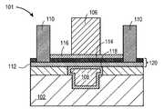
발명의 실시예들은 멀티-게이트 HEMT들 및 그 제조 방법들에 관한 것이다. 실시예에서, 멀티-게이트 HEMT는 기판의 최상부 상에 배치되는 채널층을 포함한다. 제1 게이트 전극은 채널층 위에 배치되고, 제2 게이트 전극은 채널층 아래에 배치된다. 제1 및 제2 게이트 전극들의 대향 측면들 상에 소스 및 드레인 콘택트들이 있다. 실시예들에서, 제1 및 제2 게이트 전극들은 각자, 채널층 위 및 아래로부터의 전류 흐름을 제어한다. 따라서, 멀티-게이트 HEMT는 전류 흐름의 최대 제어를 가진다.Embodiments of the invention relate to multi-gate HEMTs and methods of fabrication thereof. In an embodiment, the multi-gate HEMT includes a channel layer disposed on top of the substrate. A first gate electrode is disposed over the channel layer and a second gate electrode is disposed below the channel layer. There are source and drain contacts on opposite sides of the first and second gate electrodes. In embodiments, the first and second gate electrodes each control current flow from above and below the channel layer. Thus, a multi-gate HEMT has a maximum control of current flow.
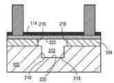
발명의 실시예에 따르면, 도 1a는 멀티-게이트 HEMT(100)의 단면도를 예시한다. 실시예에서, 멀티-게이트 HEMT(100)는 캐리어 기판(102) 상에 형성된다. 캐리어 기판(102)은 벌크 단결정질 실리콘 기판과 같은, 반도체 제조를 위한 임의의 적절한 기판으로 형성될 수 있다. 접착층(104)은 캐리어 기판(102)의 최상부 상에 형성된다. 접착층(104)은 하기에 논의될 바와 같이 캐리어 기판(102)을 또다른 기판에 부착하기 위해 사용될 수 있다. 실리콘 이산화물(SiO2)또는 알루미늄 산화물(Al2O3)과 같은 임의의 적절한 접착 재료가 사용되어 접착층(104)을 형성할 수 있다.According to an embodiment of the invention, FIG. 1A illustrates a cross-sectional view of a multi-gate HEMT 100. In an embodiment, a multi-gate HEMT 100 is formed on a
도 1a에 도시된 바와 같이, 채널층(120)은 접착층(104) 상에 배치된다. 실시예에서, 채널층(120)은 극성 반도체층(114) 및 분극층(112)을 포함하는 이종 구조체이다. 실시예들에서, 극성 반도체층(114)은 분극층(112)의 바로 위에 배치된다. 극성 반도체층(114)은, 갈륨 질화물(GaN) 또는 인듐 갈륨 질화물(InGaN)과 같은, 그러나 이에 제한되지 않는, 와이드 밴드 갭 +c 극성 반도체 재료로 형성될 수 있다. 실시예들에서, 분극층(112)은 극성 반도체층(114)에 바로 인접하게 배치될 때 2차원 전자 가스(2DEG)를 유도하는 임의의 적절한 재료로 형성된다. 예를 들어, 분극층(112)은 알루미늄 갈륨 질화물(AlGaN), 알루미늄 인듐 질화물(AlInN), 또는 알루미늄 질화물(AlN)로 형성될 수 있다.As shown in FIG. 1A, the
발명의 실시예에서, 멀티-게이트 HEMT(100)는 2개의 게이트 전극들, 즉, 제1 게이트 전극(106) 및 제2 게이트 전극(108)을 가진다. 제1 게이트 전극(106)은 채널층(120) 위에 배치될 수 있고, 제2 게이트 전극(108)은 채널층(120) 아래에 배치될 수 있다. 실시예에서, 제2 게이트 전극은 극성 반도체층(114) 아래에 배치된다. 실시예에서, 제2 게이트 전극(108)은 분극층(112) 아래에 추가로 배치된다. 도 1a에 도시된 바와 같이, 제2 게이트 전극(108)은 제1 게이트 전극(106)에 맞춰 수직으로 정렬될 수 있다. 2개의 게이트 전극을 가지는 것은 게이트 전압이 극성 반도체층(114)의 최상부 및 최하부 표면들에 인가될 수 있게 한다. 따라서, 멀티-게이트 HEMT(100)는 극성 반도체층(114)을 통해 흐르는 전류의 최대 제어를 가진다. 제1 및 제2 게이트 전극들(106 및 108)은 게이트 전극들에 대해 통상적으로 사용되는 전도성 재료로 형성될 수 있다. 실시예에서, 전도성 재료는 금속이다. 특정 실시예에서, 전도성 재료는 니켈(Ni), 티타늄 질화물(TiN), 플래티늄(Pt) 또는 텅스텐(W)으로 형성된다.In an embodiment of the invention, the multi-gate HEMT 100 has two gate electrodes, a
멀티-게이트 HEMT(100)는 2개의 게이트 유전체층들을 또한 포함한다. 제1 게이트 유전체층(116)은 극성 반도체층(114)과 제1 게이트 전극(106) 사이에 배치될 수 있다. 제2 게이트 유전체층(118)은 제2 게이트 전극(108)의 가장자리 주위에 배치될 수 있다. 실시예에서, 제2 게이트 유전체층(118)은 제2 게이트 전극(108)을 완전히 둘러싼다. 제1 및 제2 게이트 유전체층들(116 및 118)은 실리콘 산화물, 실리콘 이산화물(SiO2) 및/또는 높은-k 유전 재료와 같은, 그러나 이에 제한되지 않는, 절연 재료로 형성될 수 있다.The multi-gate HEMT 100 also includes two gate dielectric layers. A first gate
멀티-게이트 HEMT는 제1 및 제2 게이트 전극들(106 및 108)의 대향 측면들 상에 형성되는 소스 및 드레인 콘택트들을 포함한다. 실시예들에서, 소스 및 드레인 콘택트들(110)은 캐리어 기판(102) 위에 그리고 채널층(120)의 최상부 상에 배치된다. 소스 및 드레인 콘택트들(110)은 채널층(120)에 전기적으로 커플링되도록 위치된다. 실시예에서, 소스 및 드레인 콘택트들(110)은 분극층(112)의 바로 위에 배치된다. 임의의 적절한 전도성 재료가 사용되어 소스 및 드레인 콘택트들(110)을 형성할 수 있다. 실시예들에서, 소스 및 드레인 콘택트들(110)은 n-도핑된 GaN, InGaN, 또는 인듐 질화물(InN)로 형성되는 에피텍셜 반도체 구조체들이다.The multi-gate HEMT includes source and drain contacts formed on opposite sides of the first and
도 1a에 도시된 실시예에서, 멀티-게이트 HEMT(100)는 증가 모드 멀티-게이트 HEMT이다. 증가 모드 멀티-게이트 HEMT(100)는 제1 및 제2 게이트 전극들(106 및 108) 사이에 배치되는 극성 반도체층(114)을 가진다. 이 실시예에서, 분극층(112)은 제1 및 제2 게이트 전극들(106 및 108) 사이에 배치되지 않는다. 제1 및 제2 게이트 전극들(106 및 108) 사이의 분극층(112)의 부재는 제1 및 제2 게이트 전극들(106 및 108) 사이의 2DEG의 형성을 방지한다. 따라서, 증가 모드 멀티-게이트 HEMT(100)는 제1 및 제2 게이트 전극들(106 및 108) 사이에 2DEG를 가지지 않는다. 이 실시예에서, 극성 반도체층(114)은 사실상(effectively) 채널층(120)이다. 극성 반도체층(114)은 GaN 또는 InGaN과 같은 와이드 밴드 갭 반도체 재료로 형성될 수 있다.In the embodiment shown in FIG. 1A, the multi-gate HEMT 100 is an incremental mode multi-gate HEMT. The increased
증가 모드 멀티-게이트 HEMT(100)를 동작시키기 위해, 게이트 바이어스가 제1 및 제2 게이트 전극들(106 및 108)에 인가되어 극성 반도체층(114) 내의 전자들의 누적을 유도한다. 전자들의 누적은 극성 반도체층(114) 내에 역전층을 형성한다. 역전층은 소스 및 드레인 콘택트들(110) 사이의 극성 반도체층(114)을 통해 전류가 흐르도록 한다. 따라서, 게이트 바이어스를 인가하는 것은 증가 모드 멀티-게이트 HEMT(100)를 도통시킨다(ON). 그러나, 게이트 바이어스가 인가되지 않는 경우, 증가 모드 멀티-게이트 HEMT(100)는 극성 반도체층(114) 내에 역전층을 유도하지 않는다. 역전층 없이는, 극성 반도체층(114)을 통해 전류가 흐르지 않으며, 따라서, 증가 모드 멀티-게이트 HEMT(100)는 오프(OFF)이다. 발명의 실시예들에 따르면, 제1 및 제2 게이트 전극들(106 및 108)로의 게이트 바이어스의 인가는 극성 반도체층(114)의 위 및 아래로부터 채널층(120)을 제어한다. 따라서, 증가 모드 멀티-게이트 HEMT(100)는 극성 반도체층(114)을 통해 흐르는 전류의 최대 제어를 가진다.To operate the incremental
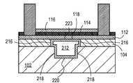
대안적인 실시예에서, 도 1b에 도시된 바와 같이, 공핍 모드 멀티-게이트 HEMT가 예시된다. 공핍 모드 멀티-게이트 HEMT(100)는 제1 및 제2 게이트 전극들(106 및 108) 사이에 배치되는 극성 반도체층(114)과 분극층(112) 양자를 가진다. 극성 반도체층(114)과 분극층(112) 사이의 상호작용들은 극성 반도체층(114)과 분극층(112) 사이의 계면에 2차원 전자 가스(2DEG)를 생성한다. 실시예들에서, 분극층(112)의 단순한 존재는 계면에 2DEG를 형성한다. 실시예에서, 2DEG는 계면으로부터 1-2 nm의 거리에 그리고 극성 반도체층(114) 내에 유도된다. 실시예에서, 극성 반도체층(114)은 와이드 밴드 갭 +C 극성 반도체 재료로 형성된다. 특정 실시예에서, 극성 반도체층(114)은 GaN 또는 InGaN로 형성된다. 분극층(112)은 극성 반도체층(114)에 바로 인접하게 배치될 때 2DEG를 유도하는 임의의 적절한 재료로 형성될 수 있다. 예를 들어, 분극층(112)은 AlGaN, AlInN, 또는 A1N으로 형성될 수 있다. 특정 실시예에서, 분극층(112)은 AlGaN으로 형성되고, 극성 반도체층(114)은 GaN으로 형성된다.In an alternative embodiment, a depletion mode multi-gate HEMT is illustrated, as shown in Figure IB. The depletion
공핍 모드 멀티-게이트 HEMT(101)를 동작시키기 위해, 게이트 바이어스가 제1 및 제2 게이트 전극들(106 및 108)에 인가되지 않는다. 2DEG를 자연적으로 형성하는 것은 소스 및 드레인 콘택트들(110) 사이에서 전류가 자유롭게 지나가도록 한다. 따라서, 공핍 모드 멀티-게이트 HEMT(101)는 게이트 바이어스가 제1 및 제2 게이트 전극들(106 및 108)에 인가되지 않을 때 항상 온(ON)이다. 게이트 바이어스가 인가될 때, 전자들이 제1 및 제2 게이트 전극들(106 및 108) 사이의 채널층(120)으로 진입하는 것이 방지된다. 채널층 내의 전자들 없이는, 채널은 핀치 오프되고, 전류가 채널층을 통해 흐를 수 없다. 따라서, 게이트 바이어스를 인가하는 것은 증가 모드 멀티-게이트 HEMT(100)를 턴 오프(turn OFF)한다. 발명의 실시예들에 따르면, 게이트 바이어스를 제1 및 제2 게이트 전극들(106 및 108)에 인가하는 것은 극성 반도체층(114)의 위 및 아래로부터 채널층(120)을 제어한다. 따라서, 공핍 모드 멀티-게이트 HEMT(101)는 채널층(120)을 통해 흐르는 전류의 최대 제어를 가진다.In order to operate the depletion
도 2a-2m은 발명의 실시예들에 따라 멀티-게이트 HEMT를 형성하는 예시적인 방법을 예시한다. 더 구체적으로, 도 2a-2j는, 발명의 실시예에 따른, 증가 모드 멀티-게이트 HEMT를 형성하는 방법의 단면도들을 예시한다. 도 2k-2m은 발명의 실시예에 따른, 도 2ga로부터 계속되는 것으로서 공핍 모드 멀티-게이트 HEMT를 형성하는 방법의 단면도들을 예시한다.Figures 2A-2M illustrate an exemplary method of forming a multi-gate HEMT in accordance with embodiments of the invention. More specifically, Figures 2A-2J illustrate cross-sectional views of a method of forming an enhanced mode multi-gate HEMT, in accordance with an embodiment of the invention. Figures 2k-2m illustrate cross-sectional views of a method for forming a depletion mode multi-gate HEMT, continuing from Figure 2ga, in accordance with an embodiment of the invention.
도 2a를 참조하면, 도너 최상부 표면(208)을 가지는 도너 기판(200)이 제공된다. 실시예에서, 도너 기판(200)은 템플릿 기판(202)의 최상부에 배치되는 두꺼운 극성 반도체층(113)을 포함한다. 도너 기판(200)은 분극층(112) 상에 배치되는 제1 접착층(104A)을 더 포함한다. 실시예들에서, 분극층(112)은 두꺼운 극성 반도체층(113) 상에 배치된다.Referring to FIG. 2A, a
도너 기판(200)을 형성하기 위한 예시적인 프로세스 흐름은 템플릿 기판(202)을 제공하는 것으로 시작할 수 있다. 템플릿 기판(202)은 다른 층들이 형성될 수 있는 베이스를 제공한다. 벌크 단결정질 실리콘 기판 또는 사파이어 기판과 같은, 그러나 이에 제한되지 않는, 임의의 적절한 기판이 템플릿 기판(202)을 형성할 수 있다.An exemplary process flow for forming the
다음으로, 두꺼운 극성 반도체층(113)이 템플릿 기판(202)의 최상부 상에 형성된다. 원자층 증착(ALD), 화학적 기상 증착(CVD), 및 분자 빔 에피텍시(MBE)와 같은 임의의 적절한 성장 프로세스가 사용되어 두꺼운 극성 반도체층(113)을 형성할 수 있다. 두꺼운 극성 반도체층(113)은 그것의 제조 동안 생성되는 결함들을 최소화시키기에 충분한 두께를 가질 수 있다. 예를 들어, GaN으로 형성되는 두꺼운 극성 반도체층(113)은 넌-네이티브 기판 상에 성장될 때 쓰레딩 전위 결함들을 형성할 수 있다. 결함들은 수직으로 전파되며, 특정 높이 이후에 결국 종료될 수 있다(terminate). 따라서, 극성 반도체층(113)의 두께는 두꺼운 극성 반도체층(113)의 상부 영역 내에서 낮은 결함 밀도를 가지는 고품질 재료를 형성하기에 충분할 필요가 있을 수 있다. 하기에 논의될 바와 같이, 두꺼운 극성 반도체층(113)의 상부 영역 내의 고품질 재료는 채널층(120)의 일부로서 추후 사용될 수 있다. 실시예에서, 두꺼운 극성 반도체층(113)의 두께는 적어도 20 ㎛이다. 특정 실시예에서, 두께는 대략 30 ㎛이다.Next, a thicker
다음으로, 분극층(112)은 에피텍셜 성장과 같은 임의의 적절한 성장 기법에 의해 두꺼운 극성 반도체층(113)의 최상부 상에 형성된다. 분극층(112)은 분극층(112)과 두꺼운 극성 반도체층(113) 사이의 계면에 2DEG를 유도하기에 충분한 두께로 형성될 수 있다. 예를 들어, 분극층(112)의 두께는 10 내지 30 nm를 범위로 할 수 있다. 특정 실시예에서, 두께는 약 20 nm이다. 분극층(112)은 두꺼운 극성 반도체층(113)과 상호작용하여 분극층(112)과 두꺼운 극성 반도체층(113) 사이의 계면에 2DEG를 유도하는 내재적 전하 극성을 가지는 임의의 적절한 재료로 형성될 수 있다. 분극층(112)에 대한 예시적인 재료들은 AlGaN, AlInN, 및AlN을 포함한다.Next, the
제1 접착층(104A)은 이후 분극층(112)의 최상부 상에 형성되고, 이에 의해, 도너 기판(200)의 형성을 완료한다. 화학적 기상 증착(CVD) 및 물리적 기상 증착(PVD)과 같은 임의의 적절한 퇴적 프로세스가 사용되어 제1 접착층(104A)을 형성할 수 있다. 제1 접착층(104A)은 도너 기판(200)을 도 2ba에 예시된 리시버 기판(201)과 같은 별도의 기판에 부착한다. 제1 접착층(104A)은 도 2ba에 예시된 제2 접착층(104B)과 같은 다른 접착층과 함께 용융될 때 강력한 결합(strong bond)을 형성하기에 충분한 두께를 가지도록 설계될 수 있다. 실시예들에서, 제1 접착층(104A)의 두께는 10nm-20nm를 범위로 한다. 제1 접착층(104A)은 SiO2 또는 A1203와 같은 접착 특징들을 가지는 임의의 적절한 재료로 형성될 수 있다. 특정 실시예에서, 도너 기판(200)은 실리콘으로 형성되는 템플릿 기판(202), GaN으로 형성되는 두꺼운 극성 반도체층(113), AlGaN으로 형성되는 분극층(112) 및 SiO2로 형성되는 제1 접착층(104A)을 포함한다.The first
선택적인 천공층(204)이 이온 클리빙(ion cleaving) 프로세스의 준비 시에 두꺼운 극성 반도체층(113) 내에 형성될 수 있다. 실시예에서, 천공층(204)은 두꺼운 극성 반도체층(113)의 성장 이후 언제든 주입된다. 실시예에서, 천공층(204)은 제1 접착층(104A)의 퇴적 이후 주입된다. 실시예에서, 천공층(204)은 두꺼운 극성 반도체층(113)의 최상부 표면(115)으로부터 깊이(D)까지의 수소 주입에 의해 생성된다. 천공층(204)은 도너 기판(200)이 이온 클리빙 프로세스에 의해 절삭될 포인트를 결정할 수 있다. 실시예들에서, 수소 주입의 깊이(D)는 도 1a에 도시된 바와 같이 채널층(120)의 일부로서 형성될 극성 반도체층(114)의 타겟 두께이다. 깊이(D) 위에 배치되는 두꺼운 극성 반도체층(113)의 일부분은 채널층(120)의 일부로서 사용되는 고품질 반도체 재료일 수 있다. 실시예에서, 깊이(D)는 적어도 2nm이다. 특정 실시예에서, 깊이(D)는 20 내지 100 nm의 범위 내에 있다.An optional
다음으로, 도 2ba에서, 리시버 최상부 표면(210)을 가지는 리시버 기판(201)이 제공된다. 실시예에서, 리시버 기판(201)은 벌크 단결정질 실리콘 기판과 같은, 반도체 제조를 위한 임의의 적절한 기판으로 형성되는 캐리어 기판(102)을 포함한다.Next, in Fig. 2b, a
희생층(206)이 리시버 기판(201) 내에 형성된다. 희생층(206)은 리시버 기판(201) 내에 완전히 임베딩될 수 있다. 도 2bb에서 리시버 기판(201)의 최상부-뷰 관점에서 보여지는 바와 같이, 희생층(206)은 제2 접착층(104B) 내의 캐리어 기판(102)의 일부분 아래로 연장할 수 있다. 도 2ba에 도시된 실시예를 다시 참조하면, 희생층(206)이 캐리어 기판(102)의 트렌치 내에 형성되고 제2 접착층(104B)에 의해 완전히 둘러싸인다. 제2 접착층(104B)은 캐리어 기판(102)의 트렌치 내의 희생층(206)을 즉시 둘러쌀 수 있다. 실시예들에서, 희생층(206)은 접착층(104B)에 대해 선택적으로 제거될 수 있는 희생 재료로 형성된다. 또한, 희생층(206)은 접착층(104B) 내로 확산하지 않는 희생 재료로 형성된다. 희생층(206)은 또한 멀티-게이트 HEMT의 다른 특징들을 형성하기 위해 사용되는 후속적인 프로세싱 조건들을 또한 견딜 수 있다. 실시예에서, 희생층(206)은 텅스텐과 같은 금속, 티타늄 질화물(TiN) 또는 실리콘 질화물(SiN)과 같은 질화물로 형성될 수 있다.A
도 2ba에 예시된 바와 같이, 제2 접착층(104B)의 일부분은 캐리어 기판(102)의 최상부 상에 배치된다. 제2 접착층(104B)은 도너 기판(200)과 같은 별도의 기판에 리시버 기판(201)을 부착할 수 있다. 실시예에서, 제2 접착층(104B)은 도 2a에서의 제1 접착층(104A)과 같은 또다른 접착층과 함께 용융될 때 강력한 결합을 형성하기에 충분한 두께를 가진다. 실시예들에서, 제2 접착층(104B)의 두께는 15-20 nm를 범위로 한다. 접착 특징들을 가지는 임의의 적절한 재료는 제2 접착층(104B)을 형성할 수 있다. 예를 들어, 제2 접착층(104B)은 SiO2 또는 Al2O3로 형성될 수 있다.As illustrated in Figure 2ba, a portion of the second
리시버 기판(201)은 널리-알려진 퇴적 및 에칭 프로세스들에 의해 형성될 수 있다. 리시버 기판(201)을 형성하기 위한 예시적인 프로세스 흐름은 이방성 에칭 프로세스를 이용하여 캐리어 기판(102) 내에 트렌치를 초기에 에칭하는 것에 의해 시작할 수 있다. 이후, 초기 접착층이 트렌치 내에 그리고 캐리어 기판(102)의 최상부 표면(103) 상에 퇴적될 수 있다. 다음으로, 희생층(206)이 초기 접착층 상에 그리고 트렌치 내에 형성된다. 평탄화 프로세스는 이후 희생층(206)의 일부분들 및 캐리어 기판(102)의 최상부 표면(103) 상에 배치되는 초기 접착층의 일부분을 제거할 수 있다. 마지막으로, 후속적인 접착층이 캐리어 기판(102)의 최상부 표면(103) 상에, 초기 접착층의 최상부 상에, 그리고 희생층(206)의 최상부 상에 퇴적될 수 있다. 초기 접착층의 나머지 부분은 후속적인 접착층과 함께 도 2ba에 예시된 바와 같이 제2 접착층(104B)을 형성한다.The
도너 기판(200) 및 리시버 기판(201)이 제공된 이후, 도너 기판(200)은 이후 리시버 기판(201)에 부착되어 도 2c에 예시된 바와 같이 결합된 기판(203)을 형성한다. 실시예에서, 도너 기판(200)을 리시버 기판(201)에 부착하는 것은 제1 접착층(104A)을 제2 접착층(104B)에 결합시킴으로써 수행된다. 제1 접착층(104A)을 제2 접착층(104B)에 결합시키는 것은 직접적인 웨이퍼 결합 프로세스에 의해 발생할 수 있다. 실시예에서, 직접적인 웨이퍼 결합 프로세스는 2개의 접착층들(104A 및 104B)의 최상부 표면들 사이에 화학적 결합을 형성한다. 직접적 웨이퍼 결합 프로세스는 산화물 용융 결합 프로세스일 수 있다. 산화물 용융 결합 프로세스는 반데르발스 힘(van der Waals force)과 같은, 정전기력을 이용하여 제자리에 2개의 접착층들(104A 및 104B)의 최상부 표면들을 임시로 고정하는 것을 포함할 수 있다. 열적 어닐링이 이후 2개의 층을 함께 화학적으로 결합시킬 수 있다.After the
실시예들에서, 접착층들(104A 및 104B)은 함께 용융되어 결합된 접착층(104)을 형성한다. 결합된 접착층(104)은 제1 및 제2 접착층들(104A 및 104B)의 합산에 의해 결정되는 두께를 가진다. 결합된 접착층(104)의 두께는 비아가 그것을 통해 형성되기에 너무 두껍지 않아야 한다. 또한, 결합된 접착층(104)의 두께는 웨이퍼 핸들링 및 후속적인 반도체 프로세싱을 견디기에 충분한 결합을 형성할 만큼 충분히 두꺼워야 한다. 실시예에서, 결합된 접착층(104)의 두께는 30 내지 40 nm를 범위로 한다.In embodiments, the
다음으로, 도 2d에 도시된 바와 같이, 결합된 기판(203)이 두꺼운 극성 반도체층(113) 내의 포인트에서 분리되어 결합된 기판(203)의 일부분(209)을 제거한다. 결합된 기판(203)의 나머지 부분은 디바이스 기판(205)을 형성한다. 디바이스 기판(205)은 발명의 실시예들에 따른 멀티-게이트 HEMT를 형성하도록 사용될 것이다. 두꺼운 극성 반도체층(113)은 부분(114x) 및 극성 반도체층(114)으로 분리된다. 부분(114x)은 폐기되거나 또는 부분(209)과의 후속적인 표면 제공(donation)들을 위해 재사용될 수 있다. 극성 반도체층(114)은 멀티-게이트 HEMT의 제조를 위한 디바이스 기판(205)의 일부분으로서 남을 수 있다. 실시예들에서, 극성 반도체층(114)은 채널층(120)이 배치되는 디바이스 기판(205)의 최상부 부분 내에 배치된다. 극성 반도체층(114)은 도 2a에 관해 위에서 논의된 두꺼운 극성 반도체층(113)의 상부 영역에 고품질 재료로 형성될 수 있다.Next, as shown in FIG. 2D, the bonded
실시예들에서, 극성 반도체층(114)은 발명의 실시예들에 따라 멀티-게이트 HEMT에 대한 채널층을 형성하기 위해 사용된다. 극성 반도체층(114)은 멀티-게이트 HEMT의 동작 동안 전류 흐름을 위해 충분한 두께를 가질 수 있다. 실시예에서, 극성 반도체층(114)의 두께는 도 2a에서 논의된 주입된 수소 원자들의 깊이(D)와 등가이다. 일 실시예에서, 극성 반도체층(114)의 두께는 적어도 2nm이다. 특정 실시예에서, 극성 반도체층(114)의 두께는 20 내지 100 nm의 범위 내에 있다.In embodiments, the
실시예에서, 결합된 기판(203)은 수소 원자들이 도 2a에 논의된 바와 같이 주입된 두꺼운 극성 반도체층(113) 내의 천공층(204)에서 이온 절삭(ion cutting)에 의해 분리된다. 이온 절삭은 수소 원자들이 주입되는 공동들을 형성하는 초기 열적 어닐링에 의해 수행될 수 있다. 공동들이 형성되면, 부분(209)은 공동들에 의해 야기되는 구조적 약화(weakness)로 인해 쉽게 분리될 수 있다. 대안적인 분리 방법들은 스폴링(spalling)과 같은 임의의 종래의 절삭 기법, 또는 임의의 적절한 선택적 에칭 릴리즈 기법을 포함한다. 본 기술분야의 통상의 기술자는 결합된 기판(203)을 분리하기 위한 선택적 에칭 릴리즈 기법을 구현하기 위해 요구되는 프로세스들을 이해할 것이다. 화학적 기계적 연마(CMP)와 같은 연마 프로세스가 이후 사용되어 최상부 표면을 평탄화(smooth)하고 층(114)을 요구되는 두께로 얇게 할 수 있다.In an embodiment, the bonded
결합된 기판(203)의 일부분(209)을 분리하고 제거한 이후, 디바이스 기판(205)은, 도 2e에 도시된 바와 같이, 발명의 실시예들에 따른 멀티-게이트 HEMT(100)를 형성하기 위해 사용된다. 실시예에서, 디바이스 기판(205)은 캐리어 기판(102), 희생층(206), 결합된 접착층(104), 및 채널층(120)을 포함한다. 실시예에서, 채널층(120)은 극성 반도체층(114) 및 분극층(112)으로 형성되는 이종 구조체이다. 실시예들에서, 극성 반도체층(114)은 분극층(112)의 바로 위에 배치된다.After separating and removing the
다음으로, 도 2f에 도시된 바와 같이, 소스 및 드레인 콘택트들(110)은 희생층(206)의 대향 측면들 상에 그리고 캐리어 기판(102) 위에 형성된다. 소스 및 드레인 콘택트들(110)은 극성 반도체층(114)으로부터 에피텍셜 성장에 의해 형성될 수 있다. 예를 들어, 소스 및 드레인 콘택트들(110)은 ALD 또는 CVD에 의해 형성될 수 있다. 실시예에서, 소스 및 드레인 콘택트들(110)은 극성 반도체층(114)을 통해 연장하고, 분극층(112)의 최상부 바로 위에 형성된다. 따라서, 소스 및 드레인 콘택트들(110)은 극성 반도체층(114) 및 분극층(112)에 커플링된다. 추가로, 소스 및 드레인 콘택트들(110)은 극성 반도체층(114) 내에 형성되는 2DEG 층에 커플링될 수 있다. 소스 및 드레인 콘택트들(110)은 임의의 적절한 반도체 재료로 형성된다. 실시예에서, 소스 및 드레인 콘택트들(110)은 n-도핑된 GaN, InGaN, 또는 InN으로 형성된다.Next, source and
하기에서, 도 2ga에 도시된 바와 같이, 희생층(206)이 선택적으로 제거되어 공동(210)을 형성한다. 실시예에서, 희생층(206)은 희생층(206)만을 실질적으로 제거하는 제1 에칭 프로세스에 의해 제거된다. 실시예에서, 제1 에칭 프로세스는 둘러싸는 결합된 접착층(104)에 대해 희생층(206)을 선택적으로 제거하는 에천트를 사용하는 등방성 습식 에칭 프로세스이다. 즉, 에천트는 희생층(206)을 실질적으로 제거하는 동시에, 둘러싸는 결합된 접착층(104)을 실질적으로 온전히(intact) 남겨둔다. 실시예에서, 에천트는 인산(H3PO4) 또는 수산화 암모늄과 과산화수소의 혼합물(NH4OH+H2O2)이다.In the following, as shown in FIG. 2Ga, the
희생층(206)을 제거하기 위해, 적어도 하나 이상의 개구들(211)이 도 2gb에 예시된 최상부-뷰 관점에서 보여지는 바와 같이 희생층(206) 바로 위의 영역(209)을 통해 형성될 수 있다. 개구들(211)은 채널층(120)을 간섭하지 않는다. 실시예에서, 개구들(211)은 희생층(206)을 노출시키고 에천트들이 흐를 수 있는 터널을 제공한다. 에천트들은 희생층(206)을 선택적으로 제거하기 위해 사용될 수 있다. 실시예들에서, 개구들(211)은 플라즈마 에칭 프로세스와 같은 임의의 적절한 에칭 프로세스에 의해 형성될 수 있다.In order to remove the
다음으로, 도 2h에 도시된 바와 같이 공동(210)이 확장되어 확대된 공동(212)을 형성한다. 실시예에서, 분극층(112)의 일부분이 제거되어 확대된 공동(212)을 형성한다. 따라서, 확대된 공동(212)은 극성 반도체층(114)의 최하부 표면(222)을 노출시킬 수 있다. 확대된 공동(212)은 디바이스 기판(205) 내의 다른 표면들을 또한 노출시킬 수 있다. 예를 들어, 확대된 공동(212)은 분극층(112)의 측벽들(214), 결합된 접착층(104)의 측벽들(216), 및 캐리어 기판(102)의 표면들(218 및 220)을 추가로 노출시킬 수 있다. 확대된 공동(212)은 도 1a-1b에 도시된 최하부 게이트 전극(108)의 게이트 길이를 정의할 수 있다. 대안적인 실시예에서, 도 2k-2m에서 하기에 추가로 논의될 바와 같이, 확대된 공동(212)은 극성 반도체층(114)을 노출시키지 않는다.Next, as shown in FIG. 2H, the
실시예들에서, 확대된 공동(212)은 2개의 에칭 프로세스들에 의해 형성된다. 예를 들어, 확대된 공동(212)은 제2 에칭 프로세스 및 제3 에칭 프로세스에 의해 형성될 수 있다. 실시예에서, 제2 에칭 프로세스는 결합된 접착층(104)의 일부분만을 실질적으로 제거한다. 제2 에칭 프로세스는 에천트를 사용하여 둘러싸는 층들(즉, 112 및 102)에 대해 결합된 접착층(104)을 실질적으로 제거하는 등방성 습식 에칭 프로세스일 수 있다. 즉, 에천트는 결합된 접착층(104)을 실질적으로 제거하는 동시에, 둘러싸는 층들을 실질적으로 온전히 남겨 둔다. 실시예에서, 에천트는 불산(HF)이다.In embodiments, the
실시예에서, 제3 에칭 프로세스는 분극층(112)의 일부분을 제거한다. 제3 에칭 프로세스는 둘러싸는 층들(즉, 114, 104 및 102)에 대해 분극층(112)을 선택적으로 제거하는 습식 에칭 프로세스일 수 있다. 즉, 에천트는 분극층(112)을 실질적으로 제거하는 동시에 둘러싸는 층들(114, 104 및 102)을 실질적으로 온전히 남겨둔다. 실시예에서, 에천트는 수산화칼륨(KOH), 수산화 나트륨(NaOH), 또는 AZ400K 포토레지스트 현상액이다.In an embodiment, a third etch process removes a portion of the
다음으로, 도 2i에 도시된 바와 같이, 제1 게이트 유전체층(116) 및 제2 게이트 유전체층(118)이 형성된다. 실시예들에서, 제1 게이트 유전체층(116)이 채널층(120)의 최상부 상에 그리고 소스 및 드레인 콘택트들(110) 사이에 형성된다. 또한, 제2 게이트 유전체층(118)은 확대된 공동(212)의 표면들(222, 214, 216, 218 및 220) 상에 형성된다. 실시예들에서, 제2 게이트 유전체층(118)은 확대된 공동(212)을 완전히 채우지는 않는다. 제1 및 제2 게이트 유전체층들(116 및 118)은 트랜지스터 동작을 위한 충분한 두께를 가지도록 형성된다. 실시예에서, 제1 및 제2 게이트 유전체층들(116 및 118)은 2-4 nm 사이의 두께를 가진다. 제1 및 제2 게이트 유전체층들(116 및 118)은 이들이 형성되는 표면들을 후속적으로 형성되는 게이트 전극들로부터 전기적으로 격리시킨다. 제1 및 제2 게이트 유전체층들(116 및 118)은 임의의 적절한 높은-k 유전 재료로 형성될 수 있다. 실시예에서, 제1 및 제2 게이트 유전체층들(116 및 118)은 SiO2, HfO2, 및 ZrO2와 같은, 그러나 이에 제한되지 않는, 절연 재료로 형성된다.Next, a first
실시예들에서, CVD 또는 ALD와 같은 임의의 적절한 순응적 퇴적 프로세스(conforming deposition process)가 제1 및 제2 게이트 유전체층들(116 및 118)을 형성할 수 있다. 실시예에서, 제1 및 제2 게이트 유전체층들(116 및 118)은 동시에 형성된다. 실시예에서, 제2 게이트 유전체층(118)은 개구들(211)을 통해 ALD에 의해 형성되고, 이는 도 2gb에서 위에서 논의된다. 따라서, 개구들(211)은 충분한 퇴적 재료가 확대된 공동(212) 내로 흘러서 제2 게이트 유전체층(118)을 퇴적시키도록 하기에 충분히 넓은 직경을 가지도록 설계되어야 한다. 실시예에서, 개구들(211)은 적어도 10 nm의 직경을 가진다. 특정 실시예에서, 개구들(211)은 15-20nm의 범위 내의 직경을 가진다.In embodiments, any suitable conforming deposition process, such as CVD or ALD, may form the first and second gate dielectric layers 116 and 118. In an embodiment, the first and second gate dielectric layers 116 and 118 are formed simultaneously. In an embodiment, a second
하기에서, 도 2j에 도시된 바와 같이, 제1 게이트 전극(106) 및 제2 게이트 전극(108)이 형성되고, 이에 의해 발명의 실시예에 따른 증가 모드 멀티-게이트 HEMT(100)의 구성을 완료한다. 제1 게이트 전극(106)은 제1 게이트 유전체층(116)의 최상부 상에 그리고 극성 반도체층(114) 위에 형성된다. 추가로, 제2 게이트 전극(108)은 극성 반도체층(114) 아래의 확대된 공동(212) 내에 형성된다. 실시예에서, 제2 게이트 전극(108)은 확대된 공동(212)을 완전히 채운다. 실시예에서, 제2 게이트 전극(108)은 제2 게이트 유전체층(118) 내에서 완전히 둘러싸인다. 제1 및 제2 게이트 전극들(106 및 108)은 설계 요건들에 따르는 게이트 길이를 가지도록 형성될 수 있다. 실시예들에서, 제1 및 제2 게이트 전극들은 극성 반도체층(114)의 깊이(D)에 종속적인 게이트 길이를 가질 수 있다. 예를 들어, 극성 반도체층(114)의 깊이(D)가 약 20 nm인 경우, 제1 및 제2 게이트 전극들(106 및 108)은 동일한 게이트 길이를 가질 수 있다. 실시예에서, 제1 및 제2 게이트 전극들(106 및 108)은 1㎛와 3㎛ 사이의 게이트 길이를 가질 수 있다. 특정 실시예에서, 제1 및 제2 게이트 전극들(106 및 108)은 2㎛의 게이트 길이를 가진다. 또다른 예에서, 극성 반도체층(114)의 깊이(D)가 약 100nm인 경우, 제1 및 제2 게이트 전극들(106 및 108)은 상이한 게이트 길이들을 가질 수 있다. 예를 들어, 제2 게이트 전극(108)은 제1 게이트 전극(106)보다 더 넓은 게이트 길이를 가질 수 있다. 실시예에서, 제1 게이트 전극(106)은 0.5㎛와 3㎛ 사이의 게이트 길이를 가질 수 있고, 제2 게이트 전극은 1㎛와 3㎛ 사이의 게이트 길이를 가질 수 있다. 특정 실시예에서, 제1 게이트 전극(106)은 1㎛의 게이트 길이를 가지고, 제2 게이트 전극(108)은 2㎛의 게이트 길이를 가진다.In the following, a
실시예에서, 제1 게이트 전극(106) 및 제2 게이트 전극(108)은 서로 수직으로 정렬된다. 추가로, 실시예에서, 제1 게이트 전극(106) 및 제2 게이트 전극(108)은 전압이 하나의 게이트에 인가될 때 다른 게이트가 또한 동일한 전압을 인가받도록 서로 전기적으로 커플링된다. 따라서, 채널층(120)의 양 측면들은 극성 반도체층(114)을 통하는 전류 흐름을 제어하는 데 사용될 수 있다. 제1 게이트 전극(106)은 임의의 적절한 게이트 형성 프로세스에 의해 형성될 수 있다. 예를 들어, 제1 게이트 전극(106)은 퇴적된 전도성 재료의 이방성 에칭에 선행하여 전도성 재료의 전반적(blanket) 퇴적에 의해 형성될 수 있다. 또다른 예에서, 제1 전극(106)은 대체 게이트 프로세스 또는 다마신(damascene) 프로세스에 의해 형성될 수 있다. 제2 게이트 전극(108)은 기판 내에 임베딩되는 공동 내에 재료를 퇴적시킬 수 있는 임의의 적절한 퇴적 기법에 의해 형성될 수 있다. 예를 들어, 제2 게이트 전극(108)은 CVD, PVD, 또는 ALD에 의해 형성될 수 있다. 특정 실시예에서, 제1 및 제2 게이트 전극들(106 및 108)이 동시에 형성된다. 제1 및 제2 게이트 전극들(106 및 108)은 제1 게이트 전극(106)을 형성하기 위한 이방성 에칭에 선행하여, CVD, PVD 또는 ALD에 의해 형성될 수 있다. 제1 및 제2 게이트 전극들(106 및 108)은 금속과 같은, 전도성 재료로 형성될 수 있다. 예시적인 금속들은 Ni, TiN, Pt, 및 W을 포함한다.In an embodiment, the
발명의 실시예에 따르면, 도 2j에 예시된 증가 모드 멀티-게이트 HEMT(100)는 제1 및 제2 게이트 전극들(106 및 108) 사이에 배치되는 극성 반도체층(114)을 가진다. 이 실시예에서, 분극층(112)은 제1 및 제2 게이트 전극들(106 및 108) 사이에 배치되지 않는다. 제1 및 제2 게이트 전극들(106 및 108) 사이의 분극층(112)의 부재는 제1 및 제2 게이트 전극들(106 및 108) 사이의 2DEG의 형성을 방지한다. 발명의 실시예들에 따르면, 제1 및 제2 게이트 전극들(106 및 108)에 게이트 바이어스를 인가하는 것은 극성 반도체층(114)의 위 및 아래로부터 채널층(120)을 제어한다. 따라서, 증가 모드 멀티-게이트 HEMT(100)는, 발명의 실시예에 따라, 극성 반도체층(114)을 통해 흐르는 전류의 최대 제어를 가진다.According to an embodiment of the invention, the enhancement
대안적인 실시예에서, 분극층(112)은 제1 및 제2 게이트 전극들(106 및 108) 사이에 온전히 남아서 공핍 모드 멀티-게이트 HEMT를 형성할 수 있다. 공핍 모드 멀티-게이트 HEMT를 형성하는 방법이 도 2k-2m에 예시되며, 이는 전술된 도 2ga로부터 계속된다.In an alternative embodiment, the
도 2k에서, 도 2ga로부터의 공동(210)이 확장되어 확대된 공동(212)을 형성한다. 이 실시예에서, 확대된 공동(212)은 극성 반도체층(114)을 노출시키지 않는다. 확대된 공동(212)은 분극층(112)의 최하부 표면(223)을 노출시킬 수 있다. 실시예들에서, 확대된 공동(212)은 결합된 접착층(104)의 측벽들(216), 및 캐리어 기판(102)의 표면들(218 및 220)을 추가로 노출시킬 수 있다. 도 2h에 관해 위에서 논의된 바와 같이, 확대된 공동(212)은 결합된 접착층(104)만을 실질적으로 제거하는 제2 에칭 프로세스에 의해 형성될 수 있다. 다음으로, 도 2l에 도시된 바와 같이, 제1 게이트 유전체층(116) 및 제2 게이트 유전체층(118)이 형성된다. 이 실시예에서, 제1 게이트 유전체층(116)은 채널층(120)의 최상부 상에 그리고 소스 및 드레인 콘택트들(110) 사이에 형성된다. 또한, 제2 게이트 유전체층(118)은 확대된 공동(212)의 표면들(223, 216, 218, 및 220) 상에 형성된다. 제2 게이트 유전체층(118)은 확대된 공동(212)을 완전히 채우지는 않는다. 실시예에서, 제2 게이트 유전체(118)의 일부분은 분극층(112) 바로 아래에 형성된다. 제1 및 제2 게이트 유전체층들(116 및 118)은 도 2i에서 기술된 것과 유사한 두께들, 디멘젼들 및 형성 프로세스 기법들을 가진다.In Figure 2K, the
하기에서, 도 2m에 도시된 바와 같이, 제1 게이트 전극(106) 및 제2 게이트 전극(108)이 형성되고, 이에 의해 발명의 실시예에 따른 공핍 모드 멀티-게이트 HEMT(101)의 구성을 완료한다. 실시예들에서, 제1 게이트 전극(106)은 제1 게이트 유전체층(116)의 최상부 상에 그리고 채널층(120) 위에 형성된다. 제2 게이트 전극(108)은 확대된 공동(212) 내에 형성된다. 제2 게이트 전극(108)은 극성 반도체층(114) 및 분극층(112)으로 형성되는 채널층(120) 아래에 배치될 수 있다. 실시예에서, 제2 게이트 전극(108)은 제2 게이트 유전체층(118)에 의해 완전히 둘러싸인다. 실시예에서, 제1 게이트 전극(106) 및 제2 게이트 전극(108)은 서로 수직으로 정렬된다. 추가로, 실시예에서, 제1 게이트 전극(106) 및 제2 게이트 전극(108)은, 전압이 하나의 게이트에 인가될 때 다른 게이트가 또한 동일한 전압을 인가받도록, 서로 전기적으로 커플링된다. 따라서, 채널층(120)의 양 측면들은 채널층(120)을 통한 전류 흐름을 제어하는 데 사용될 수 있다. 실시예에서, 제1 및 제2 게이트 전극들(106 및 108)은 도 2j에서 위에서 개시된 구조적 디멘젼들에 따라 그리고 프로세스 기법들에 의해 형성된다.In the following, a
발명의 실시예에 따르면, 공핍 모드 멀티-게이트 HEMT(101)는 제1 및 제2 게이트 전극들(106 및 108) 사이에 배치되는 극성 반도체층(114) 및 분극층(112) 둘 모두를 가진다. 따라서, 공핍 모드 멀티-게이트 HEMT(101)는 제1 및 제2 게이트 전극들(106 및 108) 사이에 2DEG를 가진다. 실시예에서, 2DEG는 극성 반도체층(114) 내의 계면으로부터 1-2 nm 떨어져 있다. 발명의 실시예들에 따르면, 제1 및 제2 게이트 전극들(106 및 108)에 게이트 바이어스를 인가하는 것은 극성 반도체층(114)의 위 및 아래로부터 채널층(120)을 제어한다. 따라서, 공핍 모드 멀티-게이트 HEMT(101)는, 발명의 실시예에 따라, 채널층(120)을 통해 흐르는 전류의 최대 제어를 가진다.According to an embodiment of the invention, depletion
도 3은 발명의 실시예들을 이용하여 제조되는 하나 이상의 다이들을 포함하는 인터포저(300)를 예시한다. 인터포저(300)는 제1 기판(302)을 제2 기판(304)에 브리징(bridge)하기 위해 사용되는 중간 기판이다. 제1 기판(302)은, 예를 들어, 집적 회로 다이일 수 있다. 제2 기판(304)은, 예를 들어, 메모리 모듈, 컴퓨터 마더보드, 또는 또다른 집적 회로 다이일 수 있다. 일반적으로, 인터포저(300)의 목적은 더 넓은 피치로 접속을 확산시키는 것 또는 접속을 상이한 접속으로 재라우팅시키는 것이다. 예를 들어, 인터포저(300)는 제2 기판(304)에 후속적으로 커플링될 수 있는 볼 그리드 어레이(BGA)(306)에 집적 회로 다이를 커플링시킬 수 있다. 일부 실시예들에서, 제1 및 제2 기판들(302/304)은 인터포저(300)의 대향 측면들 상에 부착된다. 다른 실시예들에서, 제1 및 제2 기판들(302/304)은 인터포저(300)의 동일 측에 부착된다. 추가적인 실시예들에서, 3개 이상의 기판들이 인터포저(300)에 의해 상호접속된다.Figure 3 illustrates an
인터포저(300)는 에폭시 수지, 섬유유리-강화형 에폭시 수지, 세라믹 재료, 또는 폴리이미드와 같은 폴리머 재료로 형성될 수 있다. 추가적인 구현예들에서, 인터포저는 실리콘, 게르마늄, 및 다른 III-V족 및 IV족 재료들과 같은, 반도체 기판에서 사용하기 위해 전술된 동일한 재료들을 포함할 수 있는 교번적인 강성 또는 유연성 재료들로 형성될 수 있다.The
인터포저는 금속 상호접속들(308) 및 스루-실리콘 비아(through-silicon via; TSV)들(312)을 포함하지만 이에 제한되지 않는 비아들(310)을 포함할 수 있다. 인터포저(300)는 수동 디바이스 및 능동 디바이스 모두를 포함하는, 임베딩형 디바이스들(314)을 더 포함할 수 있다. 이러한 디바이스들은, 커패시터들, 디커플링 커패시터들, 저항기들, 인덕터들, 퓨즈들, 다이오드들, 변압기들, 센서들, 및 정전기 방전(ESD) 디바이스들을 포함하지만 이에 제한되지 않는다. 라디오-주파수(RF) 디바이스들, 전력 증폭기들, 전력 관리 디바이스들, 안테나들, 어레이들, 센서들, 및 MEMS 디바이스들과 같은 더 복잡한 디바이스들이 인터포저(300) 상에 또한 형성될 수 있다.The interposer may include
발명의 실시예들에 따르면, 본원에 개시되는 멀티-게이트 HEMT들 또는 멀티-게이트 HEMT들을 형성하는 방법들이 인터포저(300)의 제조 시 사용될 수 있다.According to embodiments of the invention, methods for forming multi-gate HEMTs or multi-gate HEMTs disclosed herein may be used in the fabrication of
도 4는 발명의 일 실시예에 따른 컴퓨팅 디바이스(400)를 예시한다. 컴퓨팅 디바이스(400)는 다수의 컴포넌트들을 포함할 수 있다. 일 실시예에서, 이러한 컴포넌트들은 하나 이상의 마더보드들에 부착된다. 대안적인 실시예에서, 이러한 컴포넌트들은 마더보드보다는 단일의 시스템-온-칩(system-on-a-chip; SoC) 상에 제조된다. 컴퓨팅 디바이스(400) 내의 컴포넌트들은 집적 회로 다이(402) 및 적어도 하나의 통신 칩(408)을 포함하지만 이에 제한되지 않는다. 일부 구현예들에서, 통신 칩(408)은 집적 회로 다이(402)의 일부로서 제조된다. 집적 회로 다이(402)는 CPU(404) 뿐만 아니라, 임베딩형 DRAM(eDRAM) 또는 스핀-전송 토크 메모리(STTM 또는 STTM-RAM)과 같은 기술들에 의해 제공될 수 있는, 캐시 메모리로서 종종 사용되는, 온-다이 메모리(406)를 포함할 수 있다.Figure 4 illustrates a
컴퓨팅 디바이스(400)는 마더보드에 물리적으로 그리고 전기적으로 커플링되거나 SoC 다이 내에 제조될 수 있는, 또는 그렇지 않을 수 있는 다른 컴포넌트들을 포함할 수 있다. 이러한 다른 컴포넌트들은 휘발성 메모리(410)(예를 들어, DRAM), 비휘발성 메모리(412)(예를 들어, ROM 또는 플래시 메모리), 그래픽 프로세싱 유닛(414)(GPU), 디지털 신호 프로세서(416), 암호 프로세서(442)(하드웨어 내에서 암호(cryptographic) 알고리즘을 실행하는 특수 프로세서), 칩셋(420), 안테나(422), 디스플레이 또는 터치스크린 디스플레이(424), 터치스크린 제어기(426), 배터리(428) 또는 다른 전원, 전력 증폭기(미도시됨), 글로벌 포지셔닝 시스템(GPS) 디바이스(428), 나침반(430), 모션 코프로세서 또는 센서들(432)(가속계, 자이로스코프 및 나침반을 포함할 수 있음), 스피커(434), 카메라(436), 사용자 입력 디바이스들(438)(예컨대, 키보드, 마우스, 스타일러스 및 터치패드) 및 대용량 저장 디바이스(440)(예컨대, 하드 디스크 드라이브, 컴팩트 디스크(CD), 디지털 다목적 디스크(DVD) 등)을 포함하지만, 이에 제한되지 않는다.The
통신 칩(408)은 컴퓨팅 디바이스(400)로의 그리고 컴퓨팅 디바이스(400)로부터의 데이터의 전달을 위한 무선 통신들을 가능하게 한다. 용어 "무선" 및 그것의 파생어들은 비-고체 매체를 통한 변조된 전자기 복사의 사용을 통해 데이터를 통신할 수 있는 회로들, 디바이스들, 시스템들, 방법들, 기법들, 통신 채널들 등을 기술하기 위해 사용될 수 있다. 그 용어는 연관된 디바이스들이 어떠한 와이어들도 포함하지 않음을 내포하지는 않지만, 일부 실시예들에서 이들은 그렇지 않을 수도 있다. 통신 칩(408)은 Wi-Fi(IEEE 802.11 계열), WiMAX (IEEE 802.16 계열), IEEE 802.20, 롱 텀 에볼루션(LTE), Ev-DO, HSPA+, HSDPA+, HSUPA+, EDGE, GSM, GPRS, CDMA, TDMA, DECT, 블루투스, 이들의 파생물들, 뿐만 아니라, 3G, 4G, 5G 및 그 이상으로서 지정되는 임의의 다른 무선 프로토콜들을 포함하지만 이에 제한되지 않는 다수의 무선 표준들 또는 프로토콜들 중 임의의 것을 구현할 수 있다. 컴퓨팅 디바이스(400)는 복수의 통신 칩들(408)을 포함할 수 있다. 예를 들어, 제1 통신 칩(408)은 Wi-Fi 및 블루투스와 같은 더 단거리의 무선 통신들에 전용될 수 있고, 제2 통신 칩(408)은 GPS, EDGE, GPRS, CDMA, WiMAX, LTE, Ev-DO 등과 같은 더 장거리의 무선 통신들에 전용될 수 있다.The
컴퓨팅 디바이스(400)의 프로세서(404)는 본 발명의 실시예들 중 하나 이상의 멀티-게이트 HEMT 디바이스들을 포함할 수 있고, 이는 발명의 실시예들에 따라 형성될 수 있다. 용어 "프로세서"는 레지스터들 및/또는 메모리로부터의 전자 데이터를 프로세싱하여 그 전자 데이터를 레지스터들 및/또는 메모리에 저장될 수 있는 다른 전자 데이터로 변환시키는 임의의 디바이스 또는 디바이스의 일부분을 지칭할 수 있다.The
통신 칩(408)은 또한 본 발명의 실시예들의 하나 이상의 멀티-게이트 HEMT 디바이스들을 포함할 수 있고, 이는 발명의 실시예들에 따라 형성될 수 있다.The
추가적인 실시예들에서, 컴퓨팅 디바이스(400) 내에 하우징되는 또다른 컴포넌트는 본 발명의 실시예들 중 하나 이상의 멀티-게이트 HEMT 디바이스들을 포함할 수 있고, 이는 발명의 실시예들에 따라 형성될 수 있다.In further embodiments, another component housed within the
다양한 실시예들에서, 컴퓨팅 디바이스(400)는 랩톱 컴퓨터, 넷북 컴퓨터, 노트북 컴퓨터, 울트라북 컴퓨터, 스마트폰, 태블릿, 개인용 디지털 보조 단말(PDA), 울트라 모바일 PC, 모바일 폰, 데스크톱 컴퓨터, 서버, 프린터, 스캐너, 모니터, 셋톱 박스, 엔터테인먼트 제어 유닛, 디지털 카메라, 휴대용 음악 플레이어, 또는 디지털 비디오 레코더일 수 있다. 추가적인 구현예들에서, 컴퓨팅 디바이스(400)는 데이터를 프로세싱하는 임의의 다른 전자 디바이스일 수 있다.In various embodiments, the
실시예에서, 반도체 디바이스는 기판, 및 기판의 최상부 상의 접착층, 접착층의 최상부 상의 채널층, 채널층의 최상부 상의 제1 게이트 전극 ― 제1 게이트 전극은 제1 게이트 전극과 채널층 사이에 제1 게이트 유전체층을 가짐 ― , 채널층 아래의 제2 게이트 전극 ― 제2 게이트 전극은 제2 게이트 전극을 완전히 둘러싸는 제2 게이트 유전체층을 가짐 ―, 및 제1 전극의 대향 측면들 상의 소스 및 드레인 콘택트들의 쌍을 포함한다.In an embodiment, the semiconductor device comprises a substrate, and an adhesive layer on top of the substrate, a channel layer on top of the adhesive layer, a first gate electrode on top of the channel layer, A second gate electrode below the channel layer, a second gate electrode having a second gate dielectric layer completely surrounding the second gate electrode, and a pair of source and drain contacts on opposite sides of the first electrode, .
실시예에서, 채널층은 이종 구조체이다. 채널층은 분극층 및 분극층의 최상부 바로 위의 극성 반도체층을 포함할 수 있다. 분극층은 AlGaN으로 형성될 수 있고, 극성 반도체층은 GaN으로 형성될 수 있다. 실시예에서, 분극층은 제1 게이트 전극과 제2 게이트 전극 사이에 배치되지 않는다. 실시예에서, 극성 반도체층 및 분극층은 제1 게이트 전극과 제2 게이트 전극 사이에 배치된다. 실시예에서, 분극층은 분극층과 극성 반도체층 사이의 계면에 2차원 전자 가스(2DEG)를 유도한다. 2DEG는 극성 반도체층 내에서 계면으로부터 1-2 nm 떨어져 있을 수 있다. 실시예에서, 소스 및 드레인 콘택트들의 쌍은 극성 반도체층을 통해 분극층 상에 형성된다. 실시예에서, 제1 게이트 유전체층은 소스 및 드레인 콘택트들의 쌍 사이에 형성된다. 제2 게이트 전극은 캐리어 기판의 트렌치 내로 연장할 수 있다. 실시예에서, 제1 게이트 전극은 제2 게이트 전극에 대해 수직으로 정렬된다.In an embodiment, the channel layer is a heterologous structure. The channel layer may comprise a polarizing layer and a polarizing semiconductor layer immediately above the top of the polarizing layer. The polarizing layer may be formed of AlGaN, and the polarizing semiconductor layer may be formed of GaN. In an embodiment, the polarizing layer is not disposed between the first gate electrode and the second gate electrode. In an embodiment, the polarizing semiconductor layer and the polarizing layer are disposed between the first gate electrode and the second gate electrode. In an embodiment, the polarizing layer induces a two-dimensional electron gas (2DEG) at the interface between the polarizing layer and the polarizing semiconductor layer. The 2DEG may be located 1-2 nm from the interface in the polar semiconductor layer. In an embodiment, a pair of source and drain contacts is formed on the polarization layer through the polarity semiconductor layer. In an embodiment, a first gate dielectric layer is formed between the pair of source and drain contacts. The second gate electrode may extend into the trench of the carrier substrate. In an embodiment, the first gate electrode is aligned perpendicular to the second gate electrode.
실시예에서, 반도체 디바이스를 형성하는 방법은 도너 기판 및 리시버 기판을 제공하는 것 ― 리시버 기판은 임베딩된 희생층을 가짐 ― , 도너 기판의 일부분을 리시버 기판에 전사하여 디바이스 기판을 형성하는 것 ― 디바이스 기판의 최상부분은 채널층을 형성함 ― , 채널층 상에 그리고 임베딩된 희생층의 대향 측면들 상에 소스 및 드레인 영역들의 쌍을 형성하는 것, 임베딩된 희생층을 제거하여 채널층 아래에 공동을 형성하는 것, 채널층의 최상부 상에 제1 게이트 유전체층을 형성하고 공동 내의 측벽들 상에 제2 게이트 유전체층을 형성하는 것; 및 채널층 위의 제1 게이트 유전체층 상에 제1 게이트 전극을 형성하고 공동 내의 채널층 아래의 제2 게이트 전극 상에 제2 게이트 전극을 형성하는 것을 포함한다.In an embodiment, a method of forming a semiconductor device includes providing a donor substrate and a receiver substrate, the receiver substrate having an embedded sacrificial layer, transferring a portion of the donor substrate to a receiver substrate to form a device substrate, Forming a pair of source and drain regions on the channel layer and opposite sides of the embedded sacrificial layer; removing the embedded sacrificial layer to form a cavity below the channel layer; Forming a first gate dielectric layer on top of the channel layer and forming a second gate dielectric layer on sidewalls in the cavity; And forming a first gate electrode over the first gate dielectric layer over the channel layer and forming a second gate electrode over the second gate electrode below the channel layer in the cavity.
실시예에서, 공동을 형성하는 것은 제1 및 제2 선택적 에칭 프로세스들을 포함한다. 제1 선택적 에칭 프로세스는 희생층만을 실질적으로 제거할 수 있다. 제2 선택적 에칭 프로세스는 접착층만을 실질적으로 제거할 수 있다. 실시예에서, 제2 선택적 에칭 프로세스는 제3 선택적 에칭 프로세스를 더 포함한다. 제3 선택적 에칭 프로세스는 최하부 층의 일부분을 실질적으로 제거할 수 있다. 실시예에서, 공동을 형성하는 것은 게이트 공동 내의 최하부 층을 노출시킨다. 공동을 형성하는 것은 공동 내의 최상부 층을 노출시킬 수 있다. 실시예에서, 희생층을 선택적으로 제거하는 것은 개구들을 디바이스 기판 내로 에칭시켜서 희생층을 노출시키는 것 및 개구들을 통해 도포되는 선택적 에천트를 이용하여 희생층을 제거하는 것을 포함한다. 선택적 에천트는 둘러싸는 재료들에 대해 희생층을 선택적으로 제거할 수 있다. 실시예에서, 도너 기판의 일부분을 리시버 기판으로 전사하는 것은 도너 기판을 리시버 기판에 부착하는 것, 도너 기판을 리시버 기판에 결합시켜 결합된 기판을 형성하는 것, 및 결합된 기판을 분리시켜 디바이스 기판을 형성하는 것을 포함한다. 디바이스 기판은 리시버 기판 및 리시버 기판의 최상부 상의 도너 기판의 일부분을 포함할 수 있다. 실시예에서, 도너 기판의 일부분을 리시버 기판으로 전사하는 것은 용융 결합을 수행하여 도너 기판을 리시버 기판에 접착시키는 것을 더 포함한다.In an embodiment, forming the cavity includes first and second selective etching processes. The first selective etching process can substantially remove only the sacrificial layer. The second selective etching process can substantially remove only the adhesive layer. In an embodiment, the second selective etching process further comprises a third selective etching process. The third selective etching process may substantially remove a portion of the bottom layer. In an embodiment, forming the cavity exposes the lowermost layer in the gate cavity. Forming a cavity can expose the top layer in the cavity. In an embodiment, selectively removing the sacrificial layer includes etching the openings into the device substrate to expose the sacrificial layer and removing the sacrificial layer using an optional etchant applied through the openings. The optional etchant can selectively remove the sacrificial layer for surrounding materials. In an embodiment, transferring a portion of the donor substrate to the receiver substrate includes attaching the donor substrate to the receiver substrate, bonding the donor substrate to the receiver substrate to form a bonded substrate, Lt; / RTI > The device substrate may comprise a portion of the donor substrate on top of the receiver substrate and the receiver substrate. In an embodiment, transferring a portion of the donor substrate to the receiver substrate further comprises performing melt bonding to adhere the donor substrate to the receiver substrate.
실시예에서, 컴퓨팅 디바이스는 마더보드, 마더보드 상에 장착되는 프로세서, 및 마더보드에 장착되는 프로세서와 동일한 칩 상에 제조되는 통신 칩을 포함한다. 프로세서는 기판, 기판의 최상부 상의 접착층, 접착층의 최상부 상의 채널층, 채널층의 최상부 상의 제1 게이트 전극 ― 제1 게이트 전극은 제1 게이트 전극과 채널층 사이에 제1 게이트 유전체층을 가짐 ― , 기판 내에 그리고 채널층 아래에 임베딩되는 제2 게이트 전극 ― 제2 게이트 전극은 제2 게이트 전극을 완전히 둘러싸는 제2 게이트 유전체층을 가짐 ― , 및 제1 게이트 전극의 대향 측면들 상의 소스 및 드레인 콘택트들의 쌍을 포함한다.In an embodiment, the computing device includes a motherboard, a processor mounted on the motherboard, and a communication chip manufactured on the same chip as the processor mounted on the motherboard. A first gate electrode on the top of the channel layer, the first gate electrode having a first gate dielectric layer between the first gate electrode and the channel layer; a second gate dielectric layer on the top of the substrate, A second gate electrode embedded in and under the channel layer, a second gate electrode having a second gate dielectric layer completely surrounding the second gate electrode, and a pair of source and drain contacts on opposite sides of the first gate electrode .
실시예에서, 채널층은 이종 구조체이다. 실시예에서, 채널층은 분극층 및 분극층 바로 위의 극성 반도체층을 포함한다. 분극층은 분극층과 극성 반도체층 사이의 계면에 2차원 전자 가스(2DEG)을 유도할 수 있다. 분극층은 AlGaN으로 형성될 수 있고, 극성 반도체층은 GaN으로 형성될 수 있다. 실시예에서, 제1 게이트 전극은 제2 게이트 전극에 대해 수직으로 정렬된다.In an embodiment, the channel layer is a heterologous structure. In an embodiment, the channel layer comprises a polarizing layer and a polarizing semiconductor layer directly above the polarizing layer. The polarizing layer can induce a two-dimensional electron gas (2DEG) at the interface between the polarizing layer and the polarizing semiconductor layer. The polarizing layer may be formed of AlGaN, and the polarizing semiconductor layer may be formed of GaN. In an embodiment, the first gate electrode is aligned perpendicular to the second gate electrode.
요약서에 기술된 것을 포함하는, 발명의 예시된 구현예들의 위 기재는, 완전한 것으로 또는 발명을 개시된 정확한 형태들로 제한하도록 의도되지 않는다. 발명의 특정 구현예들 및 발명에 대한 예들이 예시의 목적으로 본원에 기술되지만, 관련 기술분야의 통상의 기술자가 인지할 바와 같이, 다양한 등가적 수정들이 발명의 범위 내에서 가능하다.The above description of exemplary implementations of the invention, including those described in the abstract, is not intended to be exhaustive or to limit the invention to the precise forms disclosed. While specific embodiments of the invention and examples of the invention are described herein for purposes of illustration, various equivalents of modifications are possible within the scope of the invention, as will be appreciated by those skilled in the art.
위의 상세한 기재의 견지에서 이러한 수정들이 발명에 대해 이루어질 수 있다. 후속하는 청구항들에서 사용되는 용어들은 발명을 명세서 및 청구항들에 개시되는 특정 구현예들로 제한하도록 해석되지 않아야 한다. 오히려, 발명의 범위는 후속하는 청구항들에 의해 전적으로 결정되며, 이는 수립된 청구항 해석의 원리들에 따라 해석될 것이다.These modifications may be made to the invention in light of the above detailed description. The terms used in the following claims should not be construed to limit the invention to the specific embodiments disclosed in the specification and claims. Rather, the scope of the invention will be determined entirely by the following claims, which will be construed in accordance with established principles of claim interpretation.
Claims (25)
Translated fromKorean기판;
상기 기판의 최상부 상의 접착층;
상기 접착층의 최상부 상의 채널층;
상기 채널층의 최상부 상의 제1 게이트 전극 ― 상기 제1 게이트 전극은 상기 제1 게이트 전극과 상기 채널층 사이에 제1 게이트 유전체층을 가짐 ― ;
상기 채널층 아래의 제2 게이트 전극 ― 상기 제2 게이트 전극은 상기 제2 게이트 전극을 완전히 둘러싸는 제2 게이트 유전체층을 가짐 ― ; 및
상기 제1 전극의 대향 측면들 상의 소스 및 드레인 콘택트들의 쌍
을 포함하는 반도체 디바이스.1. A semiconductor device comprising:
Board;
An adhesive layer on the top of the substrate;
A channel layer on top of the adhesive layer;
A first gate electrode on top of the channel layer, the first gate electrode having a first gate dielectric layer between the first gate electrode and the channel layer;
A second gate electrode below the channel layer, the second gate electrode having a second gate dielectric layer completely surrounding the second gate electrode; And
A pair of source and drain contacts on opposite sides of the first electrode
≪ / RTI >
도너(donor) 기판 및 리시버(receiver) 기판을 제공하는 단계 ― 상기 리시버 기판은 임베딩된(embedded) 희생층을 가짐 ― ;
상기 도너 기판의 일부분을 상기 리시버 기판 상에 전사(transfer)하여 디바이스 기판을 형성하는 단계 ― 상기 디바이스 기판의 최상부 부분은 채널층을 형성함 ― ;
상기 채널층 상에 그리고 상기 임베딩된 희생층의 대향 측면들 상에 소스 및 드레인 영역들의 쌍을 형성하는 단계;
상기 임베딩된 희생층을 제거하여 상기 채널층 아래에 공동(void)을 형성하는 단계;
상기 채널층의 일부분의 최상부 상에 제1 게이트 유전체층을 형성하고 상기 공동 내의 측벽들 상에 제2 게이트 유전체층을 형성하는 단계; 및
상기 채널층 위의 상기 제1 게이트 유전체층 상에 제1 게이트 전극을 형성하고 상기 공동 내의 상기 채널층 아래의 제2 게이트 전극 상에 제2 게이트 전극을 형성하는 단계
를 포함하는 방법.A method of forming a semiconductor device,
Providing a donor substrate and a receiver substrate, the receiver substrate having an embedded sacrificial layer;
Transferring a portion of the donor substrate onto the receiver substrate to form a device substrate, the uppermost portion of the device substrate forming a channel layer;
Forming a pair of source and drain regions on the channel layer and on opposite sides of the embedded sacrificial layer;
Removing the embedded sacrificial layer to form a void below the channel layer;
Forming a first gate dielectric layer on top of a portion of the channel layer and forming a second gate dielectric layer on sidewalls in the cavity; And
Forming a first gate electrode on the first gate dielectric layer over the channel layer and forming a second gate electrode on the second gate electrode under the channel layer in the cavity
≪ / RTI >
상기 도너 기판을 상기 리시버 기판에 부착하는 단계;
상기 도너 기판을 상기 리시버 기판에 결합(bonding)시켜 결합된 기판을 형성하는 단계; 및
상기 결합된 기판을 분리하여 상기 디바이스 기판을 형성하는 단계
를 포함하고, 상기 디바이스 기판은 상기 리시버 기판 및 상기 리시버 기판의 최상부 상의 상기 도너 기판의 일부분을 포함하는 방법.12. The method of claim 11, wherein transferring a portion of the donor substrate onto the receiver substrate comprises:
Attaching the donor substrate to the receiver substrate;
Bonding the donor substrate to the receiver substrate to form a bonded substrate; And
Separating the combined substrate to form the device substrate
Wherein the device substrate comprises a portion of the donor substrate on top of the receiver substrate and the receiver substrate.
마더보드;
상기 마더보드 상에 장착되는 프로세서; 및
상기 프로세서와 동일한 칩 상에 제조되거나 또는 상기 마더보드 상에 장착되는 통신 칩
을 포함하고,
상기 프로세서는:
기판;
상기 기판의 최상부 상의 접착층;
상기 접착층의 최상부 상의 채널층;
상기 채널층의 최상부 상의 제1 게이트 전극 ― 상기 제1 게이트 전극은 상기 제1 게이트 전극과 상기 채널층 사이에 제1 게이트 유전체층을 가짐 ― ;
상기 기판 내에 그리고 상기 채널층 아래에 임베딩되는 제2 게이트 전극 ― 상기 제2 게이트 전극은 상기 제2 게이트 전극을 완전히 둘러싸는 제2 게이트 유전체층을 가짐 ― ; 및
상기 제1 게이트 전극의 대향 측면들 상의 소스 및 드레인 콘택트들의 쌍
을 포함하는 컴퓨팅 디바이스.As a computing device,
Motherboard;
A processor mounted on the motherboard; And
A communication chip manufactured on the same chip as the processor or mounted on the motherboard
/ RTI >
The processor comprising:
Board;
An adhesive layer on the top of the substrate;
A channel layer on top of the adhesive layer;
A first gate electrode on top of the channel layer, the first gate electrode having a first gate dielectric layer between the first gate electrode and the channel layer;
A second gate electrode embedded within the substrate and below the channel layer, the second gate electrode having a second gate dielectric layer completely surrounding the second gate electrode; And
A pair of source and drain contacts on opposite sides of the first gate electrode,
≪ / RTI >
Applications Claiming Priority (1)
| Application Number | Priority Date | Filing Date | Title |
|---|---|---|---|
| PCT/US2014/054823WO2016039733A1 (en) | 2014-09-09 | 2014-09-09 | Multi-gate high electron mobility transistors and methods of fabrication |
Publications (2)
| Publication Number | Publication Date |
|---|---|
| KR20170051412Atrue KR20170051412A (en) | 2017-05-11 |
| KR102204259B1 KR102204259B1 (en) | 2021-01-18 |
Family
ID=55459359
Family Applications (1)
| Application Number | Title | Priority Date | Filing Date |
|---|---|---|---|
| KR1020177003140AActiveKR102204259B1 (en) | 2014-09-09 | 2014-09-09 | Multi-gate high electron mobility transistors and methods of fabrication |
Country Status (8)
| Country | Link |
|---|---|
| US (1) | US10439057B2 (en) |
| EP (1) | EP3192101A4 (en) |
| JP (1) | JP6415692B2 (en) |
| KR (1) | KR102204259B1 (en) |
| CN (1) | CN106575669B (en) |
| MY (1) | MY188298A (en) |
| TW (1) | TWI666771B (en) |
| WO (1) | WO2016039733A1 (en) |
Cited By (1)
| Publication number | Priority date | Publication date | Assignee | Title |
|---|---|---|---|---|
| KR102133367B1 (en) | 2019-02-19 | 2020-07-13 | 국방과학연구소 | High electron mobility transistor and method of manufacturing the same |
Families Citing this family (15)
| Publication number | Priority date | Publication date | Assignee | Title |
|---|---|---|---|---|
| KR102382054B1 (en) | 2014-11-05 | 2022-04-01 | 코닝 인코포레이티드 | Bottom-up electrolytic via plating method |
| US9490430B1 (en)* | 2015-06-26 | 2016-11-08 | Taiwan Semiconductor Manufacturing Company, Ltd. | Field effect transistors and methods of forming same |
| US10979012B2 (en)* | 2016-09-30 | 2021-04-13 | Intel Corporation | Single-flipped resonator devices with 2DEG bottom electrode |
| JP6901880B2 (en)* | 2017-03-17 | 2021-07-14 | 株式会社東芝 | Nitride semiconductor device |
| TWI608607B (en)* | 2017-06-23 | 2017-12-11 | 國立臺灣師範大學 | Multi-gate high electron mobility transistor with aligned internal gate and negative capacitance ferroelectric dielectrics and manufacturing method thereof |
| US10917966B2 (en)* | 2018-01-29 | 2021-02-09 | Corning Incorporated | Articles including metallized vias |
| US11024717B2 (en) | 2018-03-22 | 2021-06-01 | Kabushiki Kaisha Toshiba | Semiconductor device and method of manufacturing semiconductor device |
| TWI791888B (en)* | 2018-09-11 | 2023-02-11 | 美商美國亞德諾半導體公司 | Enhancement mode compound semiconductor field-effect transistor, semiconductor device, and method of manufacturing enhancement mode semiconductor device |
| CN111370306B (en)* | 2018-12-26 | 2023-04-28 | 中芯集成电路(宁波)有限公司上海分公司 | Fabrication method of transistor and structure of fully surrounded gate device |
| KR102605621B1 (en) | 2019-01-25 | 2023-11-23 | 삼성전자주식회사 | Method for manufacturing semiconductor device having buried gate electrodes |
| US11855198B2 (en) | 2020-04-09 | 2023-12-26 | Qualcomm Incorporated | Multi-gate high electron mobility transistors (HEMTs) employing tuned recess depth gates for improved device linearity |
| KR20210134151A (en) | 2020-04-29 | 2021-11-09 | 삼성전자주식회사 | Semiconductor device |
| DE102020128628A1 (en)* | 2020-05-28 | 2021-12-02 | Taiwan Semiconductor Manufacturing Co. Ltd. | SEMICONDUCTOR COMPONENT WITH TWO-DIMENSIONAL MATERIALS |
| WO2023058147A1 (en)* | 2021-10-06 | 2023-04-13 | 日本電信電話株式会社 | Semiconductor device |
| CN118472026B (en)* | 2024-07-11 | 2024-10-08 | 辽宁材料实验室 | Extremely-low-temperature high-electron-mobility transistor, preparation method and radio frequency amplifier |
Citations (2)
| Publication number | Priority date | Publication date | Assignee | Title |
|---|---|---|---|---|
| JP2000252470A (en)* | 1999-02-25 | 2000-09-14 | Sony Corp | Semiconductor device and manufacturing method thereof |
| US20130161698A1 (en)* | 2011-12-27 | 2013-06-27 | Fabio Alessio Marino | E-mode hfet device |
Family Cites Families (17)
| Publication number | Priority date | Publication date | Assignee | Title |
|---|---|---|---|---|
| EP1283422A1 (en)* | 2001-08-07 | 2003-02-12 | Lucent Technologies Inc. | Testbench for the validation of a device under test |
| KR100451459B1 (en) | 2003-02-10 | 2004-10-07 | 삼성전자주식회사 | Method for forming double gate electrode and method for forming a semiconductor device having the same |
| US6949761B2 (en)* | 2003-10-14 | 2005-09-27 | International Business Machines Corporation | Structure for and method of fabricating a high-mobility field-effect transistor |
| US7018901B1 (en) | 2004-09-29 | 2006-03-28 | Freescale Semiconductor, Inc. | Method for forming a semiconductor device having a strained channel and a heterojunction source/drain |
| JP4650224B2 (en)* | 2004-11-19 | 2011-03-16 | 日亜化学工業株式会社 | Field effect transistor |
| JP2008252086A (en) | 2007-03-12 | 2008-10-16 | Interuniv Micro Electronica Centrum Vzw | Tunnel field effect transistor with gate tunnel barrier |
| JP4854563B2 (en) | 2007-03-30 | 2012-01-18 | キヤノン株式会社 | Image reading apparatus and image forming apparatus |
| KR101498968B1 (en)* | 2007-07-05 | 2015-03-12 | 삼성전자주식회사 | Method and apparatus for resource determination for peer-to-peer communication in a communication system |
| JP2009135448A (en)* | 2007-11-01 | 2009-06-18 | Semiconductor Energy Lab Co Ltd | Method for manufacturing semiconductor substrate and method for manufacturing semiconductor device |
| US8362604B2 (en) | 2008-12-04 | 2013-01-29 | Ecole Polytechnique Federale De Lausanne (Epfl) | Ferroelectric tunnel FET switch and memory |
| JP5043899B2 (en)* | 2009-07-27 | 2012-10-10 | 日立オートモティブシステムズ株式会社 | EGR flow control device for internal combustion engine |
| US8440998B2 (en)* | 2009-12-21 | 2013-05-14 | Intel Corporation | Increasing carrier injection velocity for integrated circuit devices |
| US8030145B2 (en)* | 2010-01-08 | 2011-10-04 | International Business Machines Corporation | Back-gated fully depleted SOI transistor |
| US8901537B2 (en) | 2010-12-21 | 2014-12-02 | Intel Corporation | Transistors with high concentration of boron doped germanium |
| US9046761B2 (en)* | 2010-12-23 | 2015-06-02 | Intel Corporation | Lithography mask having sub-resolution phased assist features |
| JP5490061B2 (en)* | 2011-07-12 | 2014-05-14 | シャープ株式会社 | Registration method for image forming apparatus and image forming apparatus |
| KR20130053193A (en)* | 2011-11-15 | 2013-05-23 | 엘지전자 주식회사 | Nitride-based heterojunction semiconductor device and method for the same |
- 2014
- 2014-09-09WOPCT/US2014/054823patent/WO2016039733A1/enactiveApplication Filing
- 2014-09-09KRKR1020177003140Apatent/KR102204259B1/enactiveActive
- 2014-09-09MYMYPI2017700394Apatent/MY188298A/enunknown
- 2014-09-09EPEP14901471.4Apatent/EP3192101A4/ennot_activeWithdrawn
- 2014-09-09USUS15/329,216patent/US10439057B2/ennot_activeExpired - Fee Related
- 2014-09-09JPJP2017505076Apatent/JP6415692B2/enactiveActive
- 2014-09-09CNCN201480081066.6Apatent/CN106575669B/enactiveActive
- 2015
- 2015-08-04TWTW104125225Apatent/TWI666771B/enactive
Patent Citations (2)
| Publication number | Priority date | Publication date | Assignee | Title |
|---|---|---|---|---|
| JP2000252470A (en)* | 1999-02-25 | 2000-09-14 | Sony Corp | Semiconductor device and manufacturing method thereof |
| US20130161698A1 (en)* | 2011-12-27 | 2013-06-27 | Fabio Alessio Marino | E-mode hfet device |
Cited By (1)
| Publication number | Priority date | Publication date | Assignee | Title |
|---|---|---|---|---|
| KR102133367B1 (en) | 2019-02-19 | 2020-07-13 | 국방과학연구소 | High electron mobility transistor and method of manufacturing the same |
Also Published As
| Publication number | Publication date |
|---|---|
| US10439057B2 (en) | 2019-10-08 |
| US20170229565A1 (en) | 2017-08-10 |
| EP3192101A1 (en) | 2017-07-19 |
| MY188298A (en) | 2021-11-25 |
| CN106575669A (en) | 2017-04-19 |
| JP6415692B2 (en) | 2018-10-31 |
| EP3192101A4 (en) | 2018-05-23 |
| TWI666771B (en) | 2019-07-21 |
| WO2016039733A1 (en) | 2016-03-17 |
| KR102204259B1 (en) | 2021-01-18 |
| CN106575669B (en) | 2020-12-08 |
| JP2017530544A (en) | 2017-10-12 |
| TW201622148A (en) | 2016-06-16 |
Similar Documents
| Publication | Publication Date | Title |
|---|---|---|
| KR102204259B1 (en) | Multi-gate high electron mobility transistors and methods of fabrication | |
| CN109906513B (en) | Integrated circuit device with backside interconnect to deep source/drain semiconductor | |
| CN105745759B (en) | Wide band gap transistor on non-native semiconductor substrate and method of making same | |
| TW202236567A (en) | Buried power rails with self-aligned vias to trench contacts | |
| KR20160111364A (en) | III-N devices in SI trenches | |
| US11018222B1 (en) | Metallization in integrated circuit structures | |
| KR102370218B1 (en) | Well-based integration of heteroepitaxial n-type and p-type transistors | |
| US10700039B2 (en) | Silicon die with integrated high voltage devices | |
| CN110350034A (en) | Circulating type contact portion structure for semiconductor fin | |
| TW202238918A (en) | Integrated circuit structures with gate cuts above buried power rails | |
| TW202326941A (en) | Integrated circuit structures with trench contact flyover structure | |
| US20200119087A1 (en) | Techniques for monolithic co-integration of polycrystalline thin-film bulk acoustic resonator devices and monocrystalline iii-n semiconductor transistor devices | |
| TWI582912B (en) | Semiconductor structure and method of forming the same | |
| CN107078157A (en) | Self-aligned gate-last III‑N transistors | |
| CN115863345A (en) | Full ring gate integrated circuit structure with doped sub-fins | |
| US20220416057A1 (en) | Fin to fin trench contact through a metal gate cut | |
| US11777022B2 (en) | Transistors including first and second semiconductor materials between source and drain regions and methods of manufacturing the same | |
| TWI844508B (en) | Gallium nitride transistor with underfill aluminum nitride for improved thermal and rf performance and method for manufacturing the same | |
| US20190172950A1 (en) | Finfet transistor with channel stress induced via stressor material inserted into fin plug region enabled by backside reveal | |
| US20240213140A1 (en) | Integrated circuit structures having backside high | |
| US11158712B2 (en) | Field-effect transistors with buried gates and methods of manufacturing the same | |
| WO2017095398A1 (en) | Anchored through-silicon vias | |
| TWI713632B (en) | METHODS FOR OBTAINING ULTRA LOW DEFECT DENSITY GaN USING CROSS POINT TRENCH DESIGN | |
| CN115579351A (en) | Integrated circuit structure with backside self-aligned conductive feedthrough contacts | |
| CN115483210A (en) | Integrated circuit structure with backside self-aligned conductive via bars |
Legal Events
| Date | Code | Title | Description |
|---|---|---|---|
| PA0105 | International application | Patent event date:20170203 Patent event code:PA01051R01D Comment text:International Patent Application | |
| PG1501 | Laying open of application | ||
| A201 | Request for examination | ||
| PA0201 | Request for examination | Patent event code:PA02012R01D Patent event date:20190909 Comment text:Request for Examination of Application | |
| E902 | Notification of reason for refusal | ||
| PE0902 | Notice of grounds for rejection | Comment text:Notification of reason for refusal Patent event date:20200918 Patent event code:PE09021S01D | |
| E701 | Decision to grant or registration of patent right | ||
| PE0701 | Decision of registration | Patent event code:PE07011S01D Comment text:Decision to Grant Registration Patent event date:20201125 | |
| GRNT | Written decision to grant | ||
| PR0701 | Registration of establishment | Comment text:Registration of Establishment Patent event date:20210112 Patent event code:PR07011E01D | |
| PR1002 | Payment of registration fee | Payment date:20210113 End annual number:3 Start annual number:1 | |
| PG1601 | Publication of registration | ||
| PR1001 | Payment of annual fee | Payment date:20231004 Start annual number:4 End annual number:4 | |
| PR1001 | Payment of annual fee | Payment date:20241230 Start annual number:5 End annual number:5 |