KR20170050334A - Light emitting device comprising wavelength conversion structures - Google Patents
Light emitting device comprising wavelength conversion structuresDownload PDFInfo
- Publication number
- KR20170050334A KR20170050334AKR1020150151752AKR20150151752AKR20170050334AKR 20170050334 AKR20170050334 AKR 20170050334AKR 1020150151752 AKR1020150151752 AKR 1020150151752AKR 20150151752 AKR20150151752 AKR 20150151752AKR 20170050334 AKR20170050334 AKR 20170050334A
- Authority
- KR
- South Korea
- Prior art keywords
- light
- light emitting
- wavelength conversion
- layer
- semiconductor
- Prior art date
- Legal status (The legal status is an assumption and is not a legal conclusion. Google has not performed a legal analysis and makes no representation as to the accuracy of the status listed.)
- Granted
Links
- 238000006243chemical reactionMethods0.000titleclaimsabstractdescription93
- 239000004065semiconductorSubstances0.000claimsdescription134
- 238000000034methodMethods0.000claimsdescription11
- 239000003086colorantSubstances0.000abstractdescription11
- 239000000463materialSubstances0.000description22
- 239000002096quantum dotSubstances0.000description9
- OAICVXFJPJFONN-UHFFFAOYSA-NPhosphorusChemical compound[P]OAICVXFJPJFONN-UHFFFAOYSA-N0.000description8
- 150000001875compoundsChemical class0.000description7
- 239000000049pigmentSubstances0.000description7
- XLOMVQKBTHCTTD-UHFFFAOYSA-NZinc monoxideChemical compound[Zn]=OXLOMVQKBTHCTTD-UHFFFAOYSA-N0.000description4
- JNDMLEXHDPKVFC-UHFFFAOYSA-Naluminum;oxygen(2-);yttrium(3+)Chemical compound[O-2].[O-2].[O-2].[Al+3].[Y+3]JNDMLEXHDPKVFC-UHFFFAOYSA-N0.000description4
- -1gallium arsenide compoundChemical class0.000description4
- 229910019901yttrium aluminum garnetInorganic materials0.000description4
- UCKMPCXJQFINFW-UHFFFAOYSA-NSulphideChemical compound[S-2]UCKMPCXJQFINFW-UHFFFAOYSA-N0.000description3
- 230000008859changeEffects0.000description3
- 239000012535impuritySubstances0.000description3
- XEEYBQQBJWHFJM-UHFFFAOYSA-NironSubstances[Fe]XEEYBQQBJWHFJM-UHFFFAOYSA-N0.000description3
- 238000012986modificationMethods0.000description3
- 230000004048modificationEffects0.000description3
- 229910018072Al 2 O 3Inorganic materials0.000description2
- IJGRMHOSHXDMSA-UHFFFAOYSA-NAtomic nitrogenChemical compoundN#NIJGRMHOSHXDMSA-UHFFFAOYSA-N0.000description2
- 229910001218Gallium arsenideInorganic materials0.000description2
- UQSXHKLRYXJYBZ-UHFFFAOYSA-NIron oxideChemical compound[Fe]=OUQSXHKLRYXJYBZ-UHFFFAOYSA-N0.000description2
- 229910052782aluminiumInorganic materials0.000description2
- XAGFODPZIPBFFR-UHFFFAOYSA-NaluminiumChemical compound[Al]XAGFODPZIPBFFR-UHFFFAOYSA-N0.000description2
- 239000011651chromiumSubstances0.000description2
- 239000010949copperSubstances0.000description2
- 238000011161developmentMethods0.000description2
- 239000007772electrode materialSubstances0.000description2
- 239000010931goldSubstances0.000description2
- 229910052751metalInorganic materials0.000description2
- 239000002184metalSubstances0.000description2
- 239000000203mixtureSubstances0.000description2
- 150000004767nitridesChemical class0.000description2
- 229910052698phosphorusInorganic materials0.000description2
- 238000005240physical vapour depositionMethods0.000description2
- 230000006798recombinationEffects0.000description2
- 238000005215recombinationMethods0.000description2
- 229920005989resinPolymers0.000description2
- 239000011347resinSubstances0.000description2
- 229910052725zincInorganic materials0.000description2
- 239000011701zincSubstances0.000description2
- 239000011787zinc oxideSubstances0.000description2
- JBRZTFJDHDCESZ-UHFFFAOYSA-NAsGaChemical compound[As]#[Ga]JBRZTFJDHDCESZ-UHFFFAOYSA-N0.000description1
- 229910000684Cobalt-chromeInorganic materials0.000description1
- 229910000530Gallium indium arsenideInorganic materials0.000description1
- XUIMIQQOPSSXEZ-UHFFFAOYSA-NSiliconChemical compound[Si]XUIMIQQOPSSXEZ-UHFFFAOYSA-N0.000description1
- BOTDANWDWHJENH-UHFFFAOYSA-NTetraethyl orthosilicateChemical compoundCCO[Si](OCC)(OCC)OCCBOTDANWDWHJENH-UHFFFAOYSA-N0.000description1
- 229910010413TiO 2Inorganic materials0.000description1
- HCHKCACWOHOZIP-UHFFFAOYSA-NZincChemical compound[Zn]HCHKCACWOHOZIP-UHFFFAOYSA-N0.000description1
- 229910003363ZnMgOInorganic materials0.000description1
- WAIPAZQMEIHHTJ-UHFFFAOYSA-N[Cr].[Co]Chemical compound[Cr].[Co]WAIPAZQMEIHHTJ-UHFFFAOYSA-N0.000description1
- YKTSYUJCYHOUJP-UHFFFAOYSA-N[O--].[Al+3].[Al+3].[O-][Si]([O-])([O-])[O-]Chemical compound[O--].[Al+3].[Al+3].[O-][Si]([O-])([O-])[O-]YKTSYUJCYHOUJP-UHFFFAOYSA-N0.000description1
- RLAVICIPRRVIRQ-UHFFFAOYSA-N[S-2].[Cd+2].[Zn+2].[S-2].[Zn+2]Chemical compound[S-2].[Cd+2].[Zn+2].[S-2].[Zn+2]RLAVICIPRRVIRQ-UHFFFAOYSA-N0.000description1
- 229910052785arsenicInorganic materials0.000description1
- 230000004888barrier functionEffects0.000description1
- 230000005540biological transmissionEffects0.000description1
- UHYPYGJEEGLRJD-UHFFFAOYSA-Ncadmium(2+);selenium(2-)Chemical compound[Se-2].[Cd+2]UHYPYGJEEGLRJD-UHFFFAOYSA-N0.000description1
- ODINCKMPIJJUCX-UHFFFAOYSA-Ncalcium oxideInorganic materials[Ca]=OODINCKMPIJJUCX-UHFFFAOYSA-N0.000description1
- VQWFNAGFNGABOH-UHFFFAOYSA-Kchromium(iii) hydroxideChemical compound[OH-].[OH-].[OH-].[Cr+3]VQWFNAGFNGABOH-UHFFFAOYSA-K0.000description1
- 229910017052cobaltInorganic materials0.000description1
- 239000010941cobaltSubstances0.000description1
- GUTLYIVDDKVIGB-UHFFFAOYSA-Ncobalt atomChemical compound[Co]GUTLYIVDDKVIGB-UHFFFAOYSA-N0.000description1
- 239000010952cobalt-chromeSubstances0.000description1
- 239000004020conductorSubstances0.000description1
- 239000000470constituentSubstances0.000description1
- 238000007796conventional methodMethods0.000description1
- 229910052802copperInorganic materials0.000description1
- OPQARKPSCNTWTJ-UHFFFAOYSA-Lcopper(ii) acetateChemical compound[Cu+2].CC([O-])=O.CC([O-])=OOPQARKPSCNTWTJ-UHFFFAOYSA-L0.000description1
- 238000000151depositionMethods0.000description1
- QDOXWKRWXJOMAK-UHFFFAOYSA-Ndichromium trioxideChemical compoundO=[Cr]O[Cr]=OQDOXWKRWXJOMAK-UHFFFAOYSA-N0.000description1
- 230000000694effectsEffects0.000description1
- 238000000407epitaxyMethods0.000description1
- 239000003822epoxy resinSubstances0.000description1
- PCHJSUWPFVWCPO-UHFFFAOYSA-NgoldChemical compound[Au]PCHJSUWPFVWCPO-UHFFFAOYSA-N0.000description1
- 229910052737goldInorganic materials0.000description1
- 230000005484gravityEffects0.000description1
- 238000005286illuminationMethods0.000description1
- DCYOBGZUOMKFPA-UHFFFAOYSA-Niron(2+);iron(3+);octadecacyanideChemical compound[Fe+2].[Fe+2].[Fe+2].[Fe+3].[Fe+3].[Fe+3].[Fe+3].N#[C-].N#[C-].N#[C-].N#[C-].N#[C-].N#[C-].N#[C-].N#[C-].N#[C-].N#[C-].N#[C-].N#[C-].N#[C-].N#[C-].N#[C-].N#[C-].N#[C-].N#[C-]DCYOBGZUOMKFPA-UHFFFAOYSA-N0.000description1
- 238000010030laminatingMethods0.000description1
- MOUPNEIJQCETIW-UHFFFAOYSA-Nlead chromateChemical compound[Pb+2].[O-][Cr]([O-])(=O)=OMOUPNEIJQCETIW-UHFFFAOYSA-N0.000description1
- QSHDDOUJBYECFT-UHFFFAOYSA-NmercuryChemical compound[Hg]QSHDDOUJBYECFT-UHFFFAOYSA-N0.000description1
- 229910052753mercuryInorganic materials0.000description1
- 229910052759nickelInorganic materials0.000description1
- 229910052757nitrogenInorganic materials0.000description1
- 230000005693optoelectronicsEffects0.000description1
- 230000001151other effectEffects0.000description1
- 239000002245particleSubstances0.000description1
- 239000011574phosphorusSubstances0.000description1
- 229920000647polyepoxidePolymers0.000description1
- 230000008569processEffects0.000description1
- 238000012545processingMethods0.000description1
- SBIBMFFZSBJNJF-UHFFFAOYSA-Nselenium;zincChemical compound[Se]=[Zn]SBIBMFFZSBJNJF-UHFFFAOYSA-N0.000description1
- 229910052710siliconInorganic materials0.000description1
- 239000010703siliconSubstances0.000description1
- 229920002050silicone resinPolymers0.000description1
- 238000004528spin coatingMethods0.000description1
- 238000006467substitution reactionMethods0.000description1
- LFQCEHFDDXELDD-UHFFFAOYSA-Ntetramethyl orthosilicateChemical compoundCO[Si](OC)(OC)OCLFQCEHFDDXELDD-UHFFFAOYSA-N0.000description1
- 239000010409thin filmSubstances0.000description1
- 229910052984zinc sulfideInorganic materials0.000description1
- NDKWCCLKSWNDBG-UHFFFAOYSA-Nzinc;dioxido(dioxo)chromiumChemical compound[Zn+2].[O-][Cr]([O-])(=O)=ONDKWCCLKSWNDBG-UHFFFAOYSA-N0.000description1
Images


Classifications
- H01L33/50—
- H01L33/60—
- H—ELECTRICITY
- H10—SEMICONDUCTOR DEVICES; ELECTRIC SOLID-STATE DEVICES NOT OTHERWISE PROVIDED FOR
- H10H—INORGANIC LIGHT-EMITTING SEMICONDUCTOR DEVICES HAVING POTENTIAL BARRIERS
- H10H20/00—Individual inorganic light-emitting semiconductor devices having potential barriers, e.g. light-emitting diodes [LED]
- H10H20/80—Constructional details
- H10H20/85—Packages
- H10H20/851—Wavelength conversion means
- H—ELECTRICITY
- H10—SEMICONDUCTOR DEVICES; ELECTRIC SOLID-STATE DEVICES NOT OTHERWISE PROVIDED FOR
- H10H—INORGANIC LIGHT-EMITTING SEMICONDUCTOR DEVICES HAVING POTENTIAL BARRIERS
- H10H20/00—Individual inorganic light-emitting semiconductor devices having potential barriers, e.g. light-emitting diodes [LED]
- H10H20/80—Constructional details
- H10H20/85—Packages
- H10H20/855—Optical field-shaping means, e.g. lenses
- H10H20/856—Reflecting means
- H—ELECTRICITY
- H01—ELECTRIC ELEMENTS
- H01L—SEMICONDUCTOR DEVICES NOT COVERED BY CLASS H10
- H01L2924/00—Indexing scheme for arrangements or methods for connecting or disconnecting semiconductor or solid-state bodies as covered by H01L24/00
- H01L2924/10—Details of semiconductor or other solid state devices to be connected
- H01L2924/11—Device type
- H01L2924/12—Passive devices, e.g. 2 terminal devices
- H01L2924/1204—Optical Diode
- H01L2924/12041—LED
Landscapes
- Led Device Packages (AREA)
- Led Devices (AREA)
Abstract
Description
Translated fromKorean본 발명은 발광 소자에 관한 것으로, 보다 상세하게는 파장변환구조체를 통해 다양한 색을 구현할 수 있는 발광 소자에 관한 것이다.BACKGROUND OF THE INVENTION 1. Field of the Invention The present invention relates to a light emitting device, and more particularly, to a light emitting device capable of realizing various colors through a wavelength conversion structure.
발광 소자는 전압을 가하면 화합물 반도체층들의 전자와 정공의 재결합에 따른 밴드갭 에너지를 기초로 하여 빛을 내는 광전자 소자이다. 발광 소자는 처리속도가 빠르고 전력소모가 적어 광 효율성이 우수하며, 소형화가 가능한 특징이 있어, 최근, 표시용 광원에서 형광등이나 백열등 등의 조명 광원을 대체할 수 있을 것으로 기대되고 있다. 이에, 발광 소자를 조명 장치 또는 디스플레이 장치의 백 라이트(back light)를 위한 고출력 및 고효율 광원으로 응용하려는 개발이 적극적으로 진행되고 있다.The light emitting device is an optoelectronic device that emits light based on the band gap energy resulting from the recombination of electrons and holes in the compound semiconductor layers when a voltage is applied. The light emitting device is expected to be capable of replacing an illuminating light source such as a fluorescent lamp or an incandescent lamp in a display light source in recent years because it has a high processing speed, low power consumption, and excellent light efficiency. Therefore, the development of a light emitting device for application as a high-power and high-efficiency light source for a backlight of a lighting device or a display device is actively under development.
일반적으로 하나의 발광 소자는 정해진 파장의 단색광을 발광하기 때문에, 백색광을 구현하기 위해서는 R(red, 적색), G(green, 녹색), B(blue, 청색)를 조합하여 백색광을 얻거나, 형광체를 이용하여 백색광으로 변환시키는 기술이 소개되고 있다. 하지만, 종래의 기술들을 응용하여 백색광을 포함한 다양한 색의 광을 구현하고자 하는 경우, 광의 휘도가 저하되거나, 서로 다른 비중과 입도를 갖는 복수개의 형광체의 배치로 인해 최종적으로 구현되는 색이 불균일하며, 공정이 복잡한 문제점이 있다.In general, one light emitting element emits monochromatic light having a predetermined wavelength. Therefore, in order to realize white light, white light is obtained by combining R (red, red), G (green, green), B To convert the light into white light. However, when conventional techniques are applied to realize light of various colors including white light, the brightness of light is lowered, the color finally realized is uneven due to the arrangement of a plurality of phosphors having different specific gravity and particle size, The process is complicated.
상술한 문제점을 해결하기 위하여, 본 발명은 백색광을 포함한 다양한 색의 광을 용이하게 구현할 수 있는 발광 소자를 제공하는 데에 있다.In order to solve the above problems, the present invention provides a light emitting device that can easily realize light of various colors including white light.
상기 과제를 해결하기 위하여 본 발명은 서로 다른 도전형을 갖는 반도체층들 사이에 위치하는 발광층을 포함하는 반도체 적층체가 복수개 적층된 발광구조체와, 상기 발광구조체의 일면에 배치된 파장변환구조체를 포함하며, 상기 파장변환구조체는, 상기 발광구조체의 일면에 배치되어, 상기 발광구조체로부터 방출된 광의 일부만을 투과시키는 필터(filter)층, 상기 필터층의 일면에 배치되어, 상기 필터층을 투과한 광을 흡수하여 광의 파장영역을 변화시켜 방출하는 파장변환층 및 상기 파장변환층의 일면에 배치되어, 상기 파장변환층 및 상기 발광구조체에서 방출된 광을 반사시켜 외부로 방출시키는 반사층을 포함하는 것을 특징으로 하는 발광 소자를 제공할 수 있다.According to an aspect of the present invention, there is provided a semiconductor light emitting device including a light emitting structure including a plurality of semiconductor stacked layers including a light emitting layer disposed between semiconductor layers having different conductivity types, and a wavelength conversion structure disposed on one surface of the light emitting structure. , The wavelength conversion structure may include a filter layer disposed on one surface of the light emitting structure and transmitting only a part of light emitted from the light emitting structure, a light emitting layer disposed on one surface of the filter layer to absorb light transmitted through the filter layer, And a reflective layer disposed on one side of the wavelength conversion layer and reflecting the light emitted from the wavelength conversion layer and the light emitting structure and emitting the light to the outside. Device can be provided.
상기 복수개의 발광구조체에 포함된 발광층들은 각각 다른 파장영역을 갖는 광을 방출하는 것일 수 있다. 본 발명의 일 실시예에서, 상기 발광구조체는 녹색광을 발광하는 제1 반도체 적층체 및 청색광을 발광하는 제2 반도체 적층체가 순차적으로 적층된 것으로, 상기 파장변환층은 상기 녹색광 또는 상기 청색광을 흡수하여 여기되는 것일 수 있다. 또한, 본 발명의 다른 실시예에서, 상기 발광구조체는, 근자외선(near-uv)광을 발광하는 제1 반도체 적층체, 녹색광을 발광하는 제2 반도체 적층체 및 청색광을 발광하는 제3 반도체 적층체가 순차적으로 적층된 것으로, 상기 파장변환층은 상기 근자외선광, 상기 녹색광 또는 상기 청색광 중에서 선택되는 어느 하나의 광을 흡수하여 여기되는 것일 수 있다.The light emitting layers included in the plurality of light emitting structures may emit light having different wavelength regions. In one embodiment of the present invention, the light emitting structure is formed by sequentially laminating a first semiconductor laminate for emitting green light and a second semiconductor laminate for emitting blue light, and the wavelength conversion layer absorbs the green light or the blue light It may be here. Further, in another embodiment of the present invention, the light emitting structure includes a first semiconductor laminate for emitting near-UV light, a second semiconductor laminate for emitting green light, and a third semiconductor laminate for emitting blue light. And the wavelength conversion layer may be excited by absorbing any one of the near ultraviolet light, the green light, and the blue light.
상기 필터층은 상기 발광구조체에서 제1 파장영역을 갖는 광을 선택적으로 투과시키며, 상기 파장변환층은 상기 필터층을 투과한 상기 제1 파장영역을 갖는 광을 흡수하여 광의 에너지를 하향 변환(down-conversion)시켜 제2 파장영역을 갖는 광으로 방출하는 것일 수 있다.Wherein the filter layer selectively transmits light having a first wavelength range in the light emitting structure and the wavelength conversion layer absorbs light having the first wavelength range transmitted through the filter layer to down- ) To emit light having a second wavelength range.
상기 발광구조체의 타면에, 상기 발광구조체 및 상기 파장변환층에서 방출되는 광을 선택적으로 투과시키기 위한 상부필터가 더 구비될 수 있다.And an upper filter for selectively transmitting light emitted from the light emitting structure and the wavelength conversion layer may be further provided on the other surface of the light emitting structure.
본 발명의 발광 소자는 복수개의 반도체 적층체가 다중접합된 발광구조체와 파장변환구조체를 통해 백색광을 포함한 원하는 색의 광을 용이하게 구현할 수 있다.The light emitting device of the present invention can easily realize light of a desired color including white light through the light emitting structure and the wavelength conversion structure in which a plurality of semiconductor stacks are bonded together.
또한, 발광구조체 최상부에 배치된 상부필터는 파장변환구조체에 도달하는 광량을 증가시켜 파장변환구조체의 변환효율을 향상시킬 수 있다.In addition, the upper filter disposed at the top of the light emitting structure can increase the amount of light reaching the wavelength conversion structure, thereby improving the conversion efficiency of the wavelength conversion structure.
다만, 발명의 효과는 상기에서 언급한 효과로 제한되지 아니하며, 언급되지 않은 또 다른 효과들을 하기의 기재로부터 당업자에게 명확히 이해될 수 있을 것이다.However, the effects of the present invention are not limited to those mentioned above, and other effects not mentioned can be clearly understood by those skilled in the art from the following description.
도 1a 내지 도 1c는 본 발명의 일 실시예에 따른 발광 소자의 구조 및 상기 발광 소자에서 방출된 광의 흐름을 모식화한 단면도이다.
도 2a 내지 도 2b는 본 발명의 다른 실시예에 따른 발광 소자 및 상기 발광 소자에서 방출된 광의 흐름을 모식화한 단면도이다.
도 3a 내지 도 3b는 본 발명의 또 다른 실시예에 따른 발광 소자 및 상기 발광 소자에서 방출된 광의 흐름을 모식화한 단면도이다.FIGS. 1A to 1C are cross-sectional views schematically illustrating a structure of a light emitting device and a flow of light emitted from the light emitting device according to an embodiment of the present invention.
FIGS. 2A and 2B are cross-sectional views illustrating a light emitting device according to another embodiment of the present invention and a flow of light emitted from the light emitting device.
FIGS. 3A and 3B are cross-sectional views illustrating a light emitting device according to another embodiment of the present invention and a flow of light emitted from the light emitting device.
이하, 첨부된 도면을 참고하여 본 발명에 의한 실시예를 상세히 설명하면 다음과 같다. 본 발명이 여러 가지 수정 및 변형을 허용하면서도, 그 특정 실시 예들이 도면들로 예시되어 나타내어지며, 이하에서 상세히 설명될 것이다. 그러나 본 발명을 개시된 특별한 형태로 한정하려는 의도는 아니며, 오히려 본 발명은 청구항들에 의해 정의된 본 발명의 사상과 합치되는 모든 수정, 균등 및 대용을 포함한다. 명세서 전체에 걸쳐서 동일한 참고번호들은 동일한 구성요소들을 나타낸다. 도면들에 있어서, 층 및 영역들의 두께는 명확성을 기하기 위하여 과장 또는 축소된 것일 수 있다. 명세서 전체에 걸쳐서 동일한 참고번호들은 동일한 구성요소들을 나타낸다.Hereinafter, embodiments of the present invention will be described in detail with reference to the accompanying drawings. While the invention is susceptible to various modifications and alternative forms, specific embodiments thereof are shown by way of example in the drawings and will herein be described in detail. Rather, the intention is not to limit the invention to the particular forms disclosed, but rather, the invention includes all modifications, equivalents and substitutions that are consistent with the spirit of the invention as defined by the claims. Like reference numerals throughout the specification denote like elements. In the drawings, the thicknesses of the layers and regions may be exaggerated or reduced for clarity. Like reference numerals throughout the specification denote like elements.
본 발명은 서로 다른 도전형을 갖는 반도체층들 사이에 위치하는 발광층을 포함하는 반도체 적층체가 복수개 적층된 발광구조체와, 상기 발광구조체의 일면에 배치된 파장변환구조체를 포함하는 발광 소자에 관한 것이다. 상기 파장변환구조체는 상기 발광구조체의 일면에 배치되어, 상기 발광구조체로부터 방출된 광의 일부만을 투과시키는 필터층, 상기 필터층의 일면에 배치되어, 상기 필터층을 투과한 광을 흡수하여 광의 파장영역을 변화시켜 방출하는 파장변환층 및 상기 파장변환층의 일면에 배치되어, 상기 파장변환층 및 상기 발광구조체에서 방출된 광을 반사시켜 외부로 방출시키는 반사층을 포함할 수 있다. 구체적으로, 상기 서로 다른 도전형을 갖는 반도체층들은 제1 도전형 반도체층이 n형인 경우, 제2 도전형 반도체층은 p형을 갖는 것으로, 이에 상기 발광층이 n형 반도체층 및 p형 반도체층 사이에 위치하는 것을 의미할 수 있다.The present invention relates to a light emitting device including a light emitting structure in which a plurality of semiconductor laminates including a light emitting layer positioned between semiconductor layers having different conductivity types are stacked, and a wavelength conversion structure disposed on one surface of the light emitting structure. The wavelength conversion structure may include a filter layer disposed on one surface of the light emitting structure and transmitting only a part of the light emitted from the light emitting structure, a light emitting layer disposed on one surface of the filter layer to absorb light transmitted through the filter layer, And a reflective layer disposed on one side of the wavelength conversion layer and reflecting the light emitted from the wavelength conversion layer and the light emitting structure and emitting the light to the outside. When the first conductivity type semiconductor layer is n-type, the second conductivity type semiconductor layer has a p-type, and the light emitting layer is formed between the n-type semiconductor layer and the p- As shown in FIG.
도 1a는 본 발명의 일 실시예에 따른 발광 소자를 모식화한 단면도이다.1A is a cross-sectional view schematically illustrating a light emitting device according to an embodiment of the present invention.
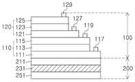
도 1a를 참조하면, 서로 다른 도전형을 갖는 반도체층들(제1 도전형 반도체층(111) 및 제2 도전형 반도체층(115)) 사이에 위치하는 제1 발광층(113)을 포함하는 제1 반도체 적층체(110)가 구비될 수 있다. 또한, 상기 제1 반도체 적층체(110) 상부에는, 서로 다른 도전형을 갖는 반도체층들(제1 도전형 반도체층(121) 및 제2 도전형 반도체층(125)) 사이에 위치하는 제2 발광층(123)을 포함하는 제2 반도체 적층체(120)가 적층되어 발광구조체(100)를 형성할 수 있다. 즉, 본 발명의 일 실시예에서, 상기 발광구조체(100)는 n형 반도체층/발광층/p형 반도체층/n형 반도체층/발광층/p형 반도체층/…으로 배치된 구조를 가질 수 있다.1A, a semiconductor light emitting device includes a first
도 1b는 본 발명의 다른 실시예에 따른 발광 소자를 모식화한 도면이다. 구체적으로 이는, 상기 도 1a의 발광구조체와 다른 구조를 가진 다른 실시예이다.1B is a schematic view of a light emitting device according to another embodiment of the present invention. Specifically, this is another embodiment having a different structure from the light emitting structure of FIG. 1A.
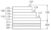
도 1b를 참조하면, 서로 다른 도전형을 갖는 반도체층들(제1 도전형 반도체층(111) 및 제2 도전형 반도체층(115)) 사이에 위치하는 제1 발광층(113)을 포함하는 제1 반도체 적층체(110)가 구비되고, 상기 제2 도전형 반도체층(115) 상부에는 제2 발광층(123)이 배치되고, 상기 제2 발광층(123) 상부에는 상기 제2 도전형 반도체층(115)과 다른 도전형을 갖는, 제1 도전형 반도체층(121)가 배치될 수 있다. 즉, 도 1b의 발광구조체(100)는 n형 반도체층/발광층/p형 반도체층/발광층/n형 반도체층…으로 배치된 구조를 가질 수 있다. 상기 제1 도전형 반도체층(111,121) 및 제2 도전형 반도체층(115, 125)는 도전성 성질을 나타낼 수 있는 불순물(dopant)이 각각 주입된 화합물 반도체층일 수 있다. 구체적으로 예를 들어, 상기 제1 도전형 반도체층(111, 121)은 규소(Si), 질소(N), 인(P) 또는 붕소(B) 등의 n형 불순물이 주입된 질화물계, 산화아연계 또는 갈륨아세나이드계의 화합물 반도체 물질을 포함할 수 있다. 또한, 상기 제2 도전형 반도체층(115, 125)는 마그네슘(Mg), 질소(N), 인(P), 비소(As), 아연(Zn), 리튬(Li) 또는 구리(Cu) 등의 p형 불순물이 주입된 질화물계, 산화아연계 또는 갈륨아세나이드계의 화합물 반도체 물질을 포함할 수 있다. 또한, 상기 각각의 반도체 적층체(110, 120)의 도전형 반도체층에 포함되는 불순물의 종류 및 첨가 농도는 실시예에 따라 다양하게 적용될 수 있다.Referring to FIG. 1B, the first
상기 발광층(113, 123)은 상기 제1 도전형 반도체층(111, 121) 및 상기 제2 도전형 반도체층(115, 125) 사이에서 전자 및 정공의 재결합에 의해 방출되는 밴드갭 에너지를 광으로 방출시키는 역할을 수행하는 것으로, 통상의 발광층 소재를 사용할 수 있다. 구체적으로 상기 발광층(113, 123)은 InxAlyGa(1-x-y)N(0≤x<1, 0≤y<1 및 0≤x+y<1)인 InAlGaN층을 우물로 하고, InaAlbGa(1-a-b)N(0≤a<1, 0≤b<1 및 0≤a+b<1)인 InAlGaN층을 장벽층으로 하는 다중양자우물(multi-quantum well, MQW) 또는 단일양자우물 구조를 가질 수 있다. 여기서, 상기 a 및 b는, 상기 x 및 y와 무관하며, 장벽 구조를 이루는 데에 목적이 있다. 또는, 상기 발광층(113, 123)을 ZnMgO 또는 ZnCdO 등의 산화아연계 물질을 포함할 수 있으며, 실시예에 따라, 상기 발광층(113, 123)은 도핑된 화합물 반도체로 이루어질 수 있다. 상기 발광층(113, 123)은 구성하는 물질의 조성비에 따라 서로 다른 파장영역을 갖는 다양한 색의 광을 방출할 수 있다. 일반적으로, 근자외선광의 파장영역은 약 300nm 내지 410nm 정도이며, 청색광의 파장영역은 440nm 내지 460nm 정도이며, 녹색광의 파장영역은 525nm 내지 535nm 정도이며, 황색광의 파장영역은 550nm 내지 600nm 정도이고, 적색광의 파장은 615nm 내지 630nm 정도이다.The
도 1a를 참조하면, 상기 제1 도전형 반도체층(111, 121) 및 상기 제2 도전형 반도체층(115, 125)에는 각각 제1 전극(117, 127) 및 제2 전극(119, 129)이 형성될 수 있다. 또한, 도 1b를 참조하면, 상기 제1 도전형 반도체층(111, 121) 및 상기 제2 도전형 반도체층(115)에는 각각 제1 전극(117, 127) 및 제 2 전극(119)이 형성될 수 있다. 상기 제1 전극(117, 127) 및 상기 제2 전극(119, 129)은 통상의 발광 소자의 전극 물질로 이루어질 수 있으며, 예를 들어 니켈(Ni), 구리(Cu), 티타늄(Ti), 알루미늄(Al) 또는 금(Au) 등의 금속 또는 광 투과성 및 전기전도도가 우수한 ITO, IZO, TiO2, ZnO, CaO 또는 WO3 등의 투명전극재료로 이루어진 군에서 선택되는 적어도 어느 하나일 수 있다. 상기 제1 전극(117, 127) 및 상기 제2 전극(119, 129)을 통해 상기 제1 반도체 적층체(110) 및 상기 제2 반도체 적층체(120)에 전압을 인가할 수 있으며, 인가된 전압에 의해 각각의 반도체 적층체(110, 120)에 포함된 상기 발광층(113, 123)들은 각각 서로 다른 파장영역을 갖는 광을 방출할 수 있게 된다.1A and 1B, first and
도 1a 내지 도 1b를 참조하면, 상기 제1 반도체 적층체(110) 및 상기 제2 반도체 적층체(120)가 순차적으로 적층된 상기 발광구조체(100)의 일면에 반사층(251), 파장변환층(231) 및 필터층(211)이 순차적으로 적층된 파장변환구조체(200)가 배치될 수 있다. 상세하게는, 상기 발광구조체(100)의 하부에 상기 발광구조체(100)로부터 방출된 광의 일부만을 투과시키는 필터층(211)이 배치되고, 상기 필터층(211)의 하부에 상기 필터층(211)을 투과한 광을 흡수하여 광의 파장영역을 변화시켜 방출하는 파장변환층(231)이 배치되며, 상기 파장변환층(231)의 하부에 상기 파장변환층(231) 및 상기 발광구조체(100)에서 방출된 광을 반사시켜 외부로 방출시키는 반사층(251)이 배치될 수 있다.1A to 1B, a
구체적으로, 상기 필터층(211)은 상기 발광구조체(100)의 각각의 반도체 적층체(110, 120)에서 방출되는 서로 다른 파장영역을 갖는 광 중에서 파장변환 하고자 하는 타겟 대상인 파장영역을 갖는 광만을 투과시켜 상기 필터층(211) 하부에 배치된 상기 파장변환층(231)에 도달하게 할 수 있다. 또한, 상기 필터층(211)은 상기 파장변환층(231)에서 에너지 하향 변환되어 변화된 파장영역으로 방출되는 광을 선택적으로 투과시켜 상기 발광구조체의 상부로 방출시키는 역할을 수행할 수 있다. 이를 통해, 본 발명은 원하는 색을 구현할 수 있는 파장영역을 갖는 광을 발광 소자의 외부로 방출시킬 수 있다.Specifically, the
상기 필터층(211)은 안료 및 안료 담체 또는 수지(투명수지, 에폭시 수지, 실리콘 수지)등을 포함하는 통상의 컬러필터 소재를 사용할 수 있다. 예를 들어, 상기 필터층(211) 구성소재로는 다이크로익 필터(dichroic filter), 장파장 투과 필터(long pass filter), 단파장 투과 필터(short pass filter), 대역 투과 필터(band pass filter) 또는 노치 필터(notch filter) 등의 유전체 필터(dielectric filter)를 사용할 수 있으나, 이에 국한되지는 않는다.The
상기 파장변환층(231)은 파장변환물질로 이루어지며, 흡수된 광에 의해 여기되어 광의 파장영역을 변화시켜 방출하는 역할을 수행할 수 있다. 구체적으로, 상기 필터층(211)이 상기 발광구조체(100)로부터 방출된 제1 파장영역을 갖는 광을 선택적으로 투과시키면, 상기 파장변환층(231)은 상기 필터층(211)을 투과한 상기 제1 파장영역을 갖는 광을 흡수하여 상기 제1 파장영역을 갖는 광의 에너지를 하향 변환(down-conversion)시켜 에너지 하향 변환에 따른 상기 제1 파장영역의 파장보다 상향된 파장영역인, 제2 파장영역을 갖는 광으로 파장영역을 변화시켜 방출할 수 있다. 상기 제1 파장영역 및 제2 파장영역은 구현하고자 하는 광에 따라 일정 범위로 설정되는 것일 수 있다.The
상기 파장변환물질은 변환하여 방출하는 광의 파장영역이 적색, 황색, 녹색 및 청색으로 이루어지는 군에서 선택되는 적어도 하나의 파장 범위를 가질 수 있도록 변환시킬 수 있는 파장변환물질을 사용할 수 있으며, 하향 변환하고자 하는 광의 파장영역에 맞춰 양자점(quantum dots, QD), 양자우물(quantum well, QW)형광체 및 안료 중에서 선택되는 적어도 어느 하나의 공지된 파장변환물질을 사용할 수 있다. 예를 들어, 상기 양자점(QD)은 Ⅱ-Ⅵ족 화합물 또는 Ⅲ-Ⅴ족 화합물로, 더욱 상세하게는, CdSe 양자점, ZnSe 양자점, InGaAs 양자점 또는 InGaN 양자점일 수 있으며, 상기 양자우물(QW)은 InGaN 양자우물층일 수 있으나, 이에 국한되지는 않는다. 상기 양자점 및 상기 양자우물은 통상의 에피택시(epitaxy)법 등을 이용하여 형성할 수 있다.The wavelength converting material may be a wavelength converting material capable of converting at least one wavelength range selected from the group consisting of red, yellow, green, and blue to a wavelength range of light converted and emitted. At least one known wavelength converting material selected from among quantum dots (QD), quantum well (QW) phosphors and pigments may be used in accordance with the wavelength region of the light. For example, the quantum dot (QD) may be a II-VI compound or a III-V compound, and more specifically, a CdSe quantum dot, a ZnSe quantum dot, an InGaAs quantum dot or an InGaN quantum dot, InGaN quantum well layer, but is not limited thereto. The quantum dots and the quantum well can be formed using a general epitaxy method or the like.
또한, 예를 들어, 적색 파장변환물질로는 SrS:Eu 또는 CaS:Eu 등의 황화물계 형광체, SrSiN:Eu, CaSiN:Eu 또는 LaSiN:Eu 등의 질화물계 형광체 또는 산화철(Fe2O3), 산화납(Pb3O4) 또는 황화수은(HgS)등의 안료를 포함할 수 있으나, 이에 한정되지는 않는다. 구체적으로 예를 들어, 황색 파장변환물질로는 YAG:Ce, TbYAG:Ce, GdYAG:Ce 또는 GdTbYAG:Ce 등의 이트륨 알루미늄 가닛(yttrium aluminum garnet, YAG)계 형광체, 메틸 실리케이트, 에틸 실리케이트, 또는 마그네슘알루미늄 실리케이트 등의 실리케이트계 형광체, 또는 황화-카드뮴-황화아연(CdS-ZnS), 크롬산 아연(ZnCrO4) 또는 크롬산 납(PbCrO4) 등의 안료를 포함할 수 있으나, 이에 한정되지는 않는다. 구체적으로 예를 들어, 녹색 파장변환물질은 BaSiO:Eu, SrSiO:Eu, SrAlO:Eu, SrAlO:Eu, SrGaS:Eu, SrSiAlON:Eu, YSiON:Tb, YSiON:Tb 또는 GdSiON:Tn의 형광체, 또는 산화크롬(Cr2O3), 수산화 크롬(Cr2O(OH)4) 또는 염기성 아세트산구리(Cu(C2H3O2)-2Cu(OH)2), 코발트크롬그린(Cr2O3-Al2O3-CoO) 등의 안료를 포함할 수 있으나, 이에 한정되지는 않는다. 구체적으로 예를 들어, 청색 파장변환물질은 Sr(PO)Cl:Eu, SrMgSiO:Eu, BaMgSiO:Eu, BaMgAlO:Eu, SrPO:Eu 또는 SrSiAlON:Eu 등의 형광체, 또는 페릭페로시아니드(Fe4[Fe(CN)6]3) 또는 코발트 블루(CoO-Al2O3)등의 안료를 포함할 수 있으나, 이에 한정되지는 않는다.As the red wavelength conversion material, for example, a sulfide-based phosphor such as SrS: Eu or CaS: Eu, a nitride-based phosphor such as SrSiN: Eu, CaSiN: Eu or LaSiN: Eu, or iron oxide (Fe2 O3 ) (Pb3 O4 ), mercury (HgS), or the like. However, the present invention is not limited thereto. Specifically, for example, the yellow wavelength conversion material may be yttrium aluminum garnet (YAG) -based phosphor such as YAG: Ce, TbYAG: Ce, GdYAG: Ce or GdTbYAG: Ce, methylsilicate, ethylsilicate, Aluminum silicate, or a pigment such as zinc sulfide-cadmium-zinc sulfide (CdS-ZnS), zinc chromate (ZnCrO4 ), or lead chromate (PbCrO4 ). Specifically, for example, the green wavelength conversion material may be a phosphor of BaSiO: Eu, SrSiO: Eu, SrAlO: Eu, SrAlO: Eu, SrGaS: Eu, SrSiAlON: Eu, YSiON: Tb, YSiON: Tb or GdSiON: chromium oxide (Cr2 O3), chromium hydroxide(Cr 2 O (OH) 4 ) or basic copper acetate(Cu (C 2 H 3 O 2) -2Cu (OH) 2), cobalt chromium green (Cr2 O3 -Al2 O3 -CoO), and the like, but it is not limited thereto. Specifically conversion, for example, a blue wavelength as material Sr (PO) Cl: Eu, SrMgSiO: Eu, BaMgSiO: Eu, BaMgAlO: Eu, SrPO: Eu or SrSiAlON: phosphor, or ferric ferro cyanide, such as Eu (Fe4 But are not limited to, pigments such as [Fe (CN)6 ]3 ) or cobalt blue (CoO-Al2 O3 ).
상기 파장변환층(231)은 공지된 형광체 또는 안료의 증착방법을 통해 형성할 수 있으며, 예를 들어, 디스펜싱(dispensing)법, 스핀코팅(spin coating)법, 물리적 기상 증착(physical vapor deposition, PVD)법 등을 이용하여 수행할 수 있다.The
도 1a를 참조하면, 상기 반사층(251)은 상기 파장변환층(231)의 일면에 배치되어, 상기 파장변환층(231) 및 상기 발광구조체(100)에서 방출하는 광을 반사시켜 발광소자의 외부로 방출시키는 기능을 수행할 수 있으며, 또한, 상기 파장변환층(231)을 통과하였으나 변환되지 않은 광의 일부도 반사시킬 수 있다. 상기 반사층(251)은 통상의 조명 장치에서 사용되는 반사층 소재를 적용할 수 있으며, 예를 들어, 알루미늄(Al) 박막과 같은 광을 반사시키는 금속층을 사용할 수 있으나, 이에 국한되지는 않는다.1A, the
상기와 같이, 본 발명은 복수개의 반도체 적층체가 접합된 발광구조체의 일면에 파장변환구조체를 구비함으로써, 상기 파장변환구조체를 통해 상기 발광구조체에서 방출되는 광의 일부를 원하는 파장영역을 갖는 광으로 변환하여 방출시킬 수 있어, 상기 발광구조체에서 방출되는 광과 함께 다양한 색을 갖는 광을 용이하게 구현할 수 있다.As described above, according to the present invention, the wavelength conversion structure is provided on one surface of the light emitting structure to which the plurality of semiconductor stacks are bonded, thereby converting part of the light emitted from the light emitting structure through the wavelength conversion structure into light having a desired wavelength range And light having various colors can be easily realized together with light emitted from the light emitting structure.
도 1c는 전술된 도 1a 내지 도 1b의 구조를 갖는 발광 소자에서 방출되는 광의 흐름을 모식화한 단면도이다. 도 1c를 참조하면, 상기 제1 반도체 적층체(110)에서 발광된 광의 일부는 상기 발광구조체(100)의 상부로 방출되고, 광의 일부는 상기 필터층(211)을 투과하여 상기 파장변환층(231)에 도달하게 된다. 상기 파장변환층(231)에 도달한 상기 제1 반도체 적층체(110)로부터 발광된 광은 상기 파장변환층(231)에 의해 광의 파장영역이 변환되어 상기 제1 반도체 적층체(110)에서 발광시의 파장영역과 다른 파장영역을 갖는 광이 되고, 이러한 광은 상기 반사층(251)에 의해 상기 발광구조체(100)의 상부로 방출될 수 있다. 이에, 상기 발광구조체(100)의 상부로 방출된 광은 상기 제2 반도체 적층체(120)에서 방출된 광, 상기 제1 반도체 적층체(110)에서 방출된 광 및 상기 파장변환층(231)에서 방출된 광이 혼합된 것으로, 각각의 광의 파장영역에 따라 다양한 색을 구현할 수 있다.FIG. 1C is a cross-sectional view schematically illustrating the flow of light emitted from the light emitting device having the structure of FIGS. 1A to 1B. 1C, a part of the light emitted from the
상기와 같이, 본 발명은 발광구조체와 파장변환층 사이에 필터층을 배치하여 상기 발광구조체에서 방출되는 광의 일부만을 통과시킴으로써 원하는 파장영역을 갖는 광으로 변환하여 파장영역이 변환된 광 및 필터층을 통과하지 않고 반사된 광을 모두 활용할 수 있으므로, 발광 소자에서 최종적으로 방출되는 광의 파장영역을 용이하게 제어할 수 있다.As described above, according to the present invention, a filter layer is disposed between the light emitting structure and the wavelength conversion layer to pass only a part of light emitted from the light emitting structure, thereby converting the light into light having a desired wavelength range, It is possible to easily control the wavelength range of the finally emitted light in the light emitting device.
본 발명의 일 실시예에서, 상기 발광구조체(100)는 녹색광을 발광하는 제1 반도체 적층체(110) 및 청색광을 발광하는 제2 반도체 적층체(120)가 순차적으로 적층된 것으로, 상기 파장변환층(231)은 상기 녹색광 또는 상기 청색광을 흡수하여 여기되는 것일 수 있다. 상기 파장변환층(231)에 흡수된 녹색광 또는 청색광은 상기 파장변환층(231)을 구성하는 형광체 및 안료 등의 파장변화물질의 조성에 따라 적색광, 황색광 또는 녹색광 등으로 변환되어 방출될 수 있다. 예를 들어, 상기 필터층(211)을 통해 상기 제1 반도체 적층체(110)의 녹색광이 투과되어 상기 파장변환층(231)에 도달되고, 상기 파장변환층(231)이 황색광을 방출하는 YAG계 형광체를 포함하는 경우, 상기 파장변환층(231)에 도달된 청색광은 상기 YAG계 형광체로 이루어진 상기 파장변환층(231)을 여기시켜 황록색의 형광으로 발생되어 상기 발광구조체(100)의 외부로 방출될 수 있다. 이에, 상기 발광 소자는 상기 제1 반도체 적층체(110)에서 방출된 녹색광, 상기 제2 반도체 적층체(120)에서 방출된 청색광 및 상기 파장변환층(231)에서 변환되어 방출된 황록색광이 합성되어 백색광을 구현할 수 있다.In one embodiment of the present invention, the
도 2a는 본 발명의 다른 실시예에 따른 발광 소자를 모식화한 단면도이다.2A is a schematic cross-sectional view of a light emitting device according to another embodiment of the present invention.
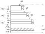
도 2a를 참조하면, 서로 다른 도전형을 갖는 반도체층들(제1 도전형 반도체층(131), 제2 도전형 반도체층(135)) 사이에 위치하는 발광층(133)을 포함하는 제1 반도체 적층체(130)가 구비될 수 있다. 상기 제1 반도체 적층체(130) 상부에는, 서로 다른 도전형을 갖는 반도체층들(제1 도전형 반도체층(141), 제2 도전형 반도체층(145)) 사이에 위치하는 발광층(143)을 포함하는 제2 반도체 적층체(140)가 구비될 수 있다. 상기 제2 반도체 적층체(140) 상부에는, 서로 다른 도전형을 갖는 반도체층들(제1 도전형 반도체층(151), 제2 도전형 반도체층(155)) 사이에 위치하는 발광층(153)을 포함하는 제3 반도체 적층체(150)가 적층되어 발광구조체(100)를 형성할 수 있다. 또한, 상기 제1 도전형 반도체층(131, 141, 151) 및 상기 제2 도전형 반도체층(135, 145, 155)에는 각각 제1 전극(137, 147, 157) 및 제2 전극(139, 149, 159)이 형성될 수 있다.2A, a
도 2a를 참조하면, 상기 3개의 반도체 적층체(130, 140, 150)가 접합된 상기 발광구조체(100)의 하부에 상기 발광구조체(100)로부터 방출된 광의 일부만을 투과시키는 필터층(213)이 배치되고, 상기 필터층(213)의 하부에 상기 필터층(213)을 투과한 광을 흡수하여 광의 파장영역을 변화시켜 방출하는 파장변환층(233)이 배치되며, 상기 파장변환층(233)의 하부에 상기 파장변환층(233)에서 방출된 광을 반사시켜 외부로 방출시키는 반사층(253)이 배치될 수 있다. 상술한 각각의 구성요소의 대한 기능 및 특징에 대한 설명은 도 1a에 개시된 바와 동일하므로, 이에 대한 상세한 설명은 도 1a를 참조할 수 있다.2A, a
도 2b는 전술된 도 2a의 구조를 갖는 발광 소자에서 방출되는 광의 흐름을 모식화한 단면도이다.FIG. 2B is a cross-sectional view schematically illustrating the flow of light emitted from the light emitting device having the structure of FIG. 2A described above.
도 2b를 참조하면, 상기 제1 반도체 적층체(130)에서 발광된 광의 일부는 상기 발광구조체(100)의 상부로 방출되고, 광의 일부는 상기 필터층(213)을 투과하여 상기 파장변환층(233)에 도달하게 된다. 상기 파장변환층(233)에 도달한 상기 제1 반도체 적층체(130)로부터 발광된 광은, 상기 파장변환층(233)에 의해 광의 파장영역이 변환되어 상기 제1 반도체 적층체(130)에서 발광시의 파장영역과 다른 파장영역을 갖는 광이 되고, 이러한 광은 상기 반사층(253)에 의해 상기 발광구조체(100)의 상부로 방출될 수 있다. 이에, 상기 발광구조체(100)의 상부로 방출된 광은 상기 제2 반도체 적층체(140)에서 방출된 광, 상기 제3 반도체 적층체(150)에서 방출된 광, 상기 제1 반도체 적층체(130)에서 방출된 광 및 상기 파장변환층(233)에서 방출된 광이 혼합된 것으로, 각각의 광의 파장영역에 따라 다양한 색을 구현할 수 있다.2B, a part of the light emitted from the
본 발명의 일 실시예에서, 상기 발광구조체(100)는, 근자외선광을 발광하는 제1 반도체 적층체(130), 녹색광을 발광하는 제2 반도체 적층체(140) 및 청색광을 발광하는 제3 반도체 적층체(150)가 순차적으로 적층된 것으로, 상기 파장변환층(233)은 상기 근자외선광, 상기 녹색광 또는 상기 청색광 중에서 선택되는 어느 하나의 광을 흡수하여 여기되는 것일 수 있다. 예를 들어, 상기 필터층(213)을 통해 상기 제1 반도체 적층체(130)의 근자외선광이 투과되어 상기 파장변환층(233)에 도달되고, 상기 파장변환층(233)이 적색광을 방출하는 황화물계 형광체를 포함하는 경우, 상기 파장변환층(233)에 도달된 근자외선광은 상기 황화물계 형광체로 이루어진 상기 파장변환층(233)을 여기시켜 적색광으로 발생되어 상기 발광구조체(100)의 외부로 방출될 수 있다. 이에, 상기 발광 소자는 상기 제3 반도체 적층체(150)에서 방출된 청색광, 상기 제2 반도체 적층체(140)에서 방출된 녹색광, 상기 제1 반도체 적층체(130)에서 방출된 근자외선광 및 상기 파장변환층(233)에서 변환되어 방출된 적색광이 합성되어 백색광을 구현할 수 있다.In one embodiment of the present invention, the
전술된 도 2a 및 도 2b와 같이, 본 발명은 반도체 적층체를 다중 접합하여 각각의 반도체 적층체들로부터 방출된 광을 합성하여 다양한 색의 광을 용이하게 구현할 수 있다. 이러한 구조적 특징을 통해 본 발명은, 종래의 다양한 색의 광을 구현하기 위해 하나의 반도체 적층체에 다양한 형광체를 복수개 배치하는 경우 휘도가 저하되고 색이 불균일했던 문제점을 개선할 수 있으며, 광의 휘도를 유지하면서도 파장변환구조체를 이용하여 광의 색을 용이하게 제어할 수 있다. 이에, 본 발명의 발광 소자는 디스플레이(display) 등의 표시 장치의 화소나 관련분야에 적극 활용될 수 있다.As shown in FIGS. 2A and 2B, the present invention can easily realize various colors of light by combining the light emitted from the respective semiconductor stacks by multiple bonding the semiconductor stacks. According to the present invention, a plurality of phosphors are arranged in a single semiconductor stacked body in order to realize light of various colors in the related art. The present invention can solve the problem that luminance is uneven and color is uneven, It is possible to easily control the color of the light using the wavelength conversion structure. Accordingly, the light emitting device of the present invention can be positively utilized in a pixel or a related field of a display device such as a display.
본 발명의 또 다른 실시예에서, 상기 발광구조체의 타면에, 상기 발광구조체 및 상기 파장변환층에서 방출되는 광을 선택적으로 투과시키기 위한 상부필터가 더 구비될 수 있다.In another embodiment of the present invention, an upper filter may be further provided on the other surface of the light emitting structure to selectively transmit light emitted from the light emitting structure and the wavelength conversion layer.
도 3a는 본 발명의 또 다른 실시예에 따른 발광 소자를 모식화한 단면도이다. 구체적으로 이는, 도 2a의 구조에서 발광구조체의 타면에 상부필터를 더 배치한 것일 수 있다.3A is a schematic cross-sectional view illustrating a light emitting device according to another embodiment of the present invention. Specifically, it may be that an upper filter is further disposed on the other surface of the light emitting structure in the structure of FIG. 2A.
도 3a를 참조하면, 서로 다른 도전형을 갖는 반도체층들(제1 도전형 반도체층(161), 제2 도전형 반도체층(165)) 사이에 위치하는 제1 발광층(163)을 포함하는 제1 반도체 적층체(160)가 구비될 수 있다. 상기 제1 반도체 적층체(160) 상부에는 제2 발광층(173)이 배치되고, 상기 제2 발광층(173) 상부에는 상기 제1 반도체 적층체(160)의 제2 도전형 반도체층(165)과 다른 도전형을 갖는 제1 도전형 반도체층(171)이 배치되어 제2 반도체 적층체(170)가 형성될 수 있다. 상기 제2 반도체 적층체(170) 상부에는, 제3 발광층(183)이 배치되고, 상기 제3 발광층(183) 상부에는 상기 제2 반도체 적층체(170)의 제1 도전형 반도체층(171)과 다른 도전형을 갖는 제2 도전형 반도체(185)가 배치되어 제3 반도체 적층체(180)가 형성되어, 상기 제1 반도체 적층체(160), 상기 제2 반도체 적층체(170) 및 상기 제3 반도체 적층체(180)를 포함하는 발광구조체(100)를 형성할 수 있다. 또한, 상기 제1 도전형 반도체층(161, 171) 및 상기 제2 도전형 반도체층(165, 185)에는 각각 제1 전극(167, 177) 및 제2 전극(179, 189)이 형성될 수 있다.Referring to FIG. 3A, a semiconductor light emitting device includes a first
상기 3개의 반도체 적층체(160, 170, 180)가 접합된 상기 발광구조체(100)의 하부에 상기 발광구조체(100)로부터 방출된 광의 일부만을 투과시키는 필터층(215)이 배치되고, 상기 필터층(215)의 하부에 상기 필터층(215)을 투과한 광을 흡수하여 광의 파장영역을 변화시켜 방출하는 파장변환층(235)이 배치되며, 상기 파장변환층(235)의 하부에 상기 파장변환층(235)에서 방출된 광을 반사시켜 외부로 방출시키는 반사층(255)이 배치될 수 있다. 상술한 각각의 구성요소의 기능 및 특징에 대한 설명은 도 1a에 개시된 바와 동일하므로, 이에 대한 상세한 설명은 도 1a를 참조할 수 있다.A
도 3a를 참조하면, 상기 발광구조체(100)의 타면, 즉, 상기 발광구조체(100)의 최상부에 상부필터(310)가 더 배치될 수 있다. 상기 상부필터(310)는 상기 발광구조체(100)를 구성하는 각각의 반도체 적층체(160, 170, 180)에서 방출된 광들 및 상기 파장변환층(235)에서 방출된 광을 선택적으로 투과시키기는 역할을 수행하는 것으로, 구현하고자 하는 광의 색에 따라 최종적으로 상기 발광 소자에서 방출되는 광의 파장영역을 선택하는 필터기능을 수행할 수 있다. 이를 통해, 본 발명은 백색광을 포함한 다양한 색의 광을 구현하도록 제어하는 것이 용이해질 수 있다.Referring to FIG. 3A, an
도 3b는 전술된 도 3a의 구조를 갖는 발광 소자에서 방출되는 광의 흐름을 모식화한 단면도이다.FIG. 3B is a cross-sectional view schematically illustrating the flow of light emitted from the light emitting device having the structure of FIG. 3A.
도 3b를 참조하면, 상기 제1 반도체 적층체(160)에서 발광된 광의 일부는 상기 발광구조체(100)의 상부 방향으로 방출되고 다른 광의 일부는 상기 제1 반도체 적층체(160) 하부에 배치된 필터층(215)으로 방출되나, 상기 발광구조체(100)의 상부로 방출된 광은 상기 발광구조체(100)의 상부에 배치된 상부필터(310)에 의해 반사되어 최종적으로 상기 발광 소자의 외부로 방출되지 않도록 제어할 수 있다. 반사된 광은 상기 제1 반도체 적층체(160) 하부에 배치된 필터층(215)을 투과하여 상기 필터층(215) 하부에 배치된 파장변환층(235)에 도달하여 파장변환되어 상기 상부필터(310)를 투과할 수 있다. 즉, 전술된 바와 같이, 상기 발광구조체(100) 상부에 필터층(310)을 구비함으로써 상기 변환하고자 하는 광을 손실없이 상기 필터층(215)을 통해 상기 파장변환층(235)으로 도달하게 할 수 있어, 발광구조체 최상부에 배치된 필터층은 파장변환구조체에 도달하는 광량을 증가시키고, 이에 파장변환구조체의 변환효율을 향상시킬 수 있다. 예를 들어, 상기 상부필터(310)의 구성소재로는 다이크로익 필터(dichroic filter), 장파장 투과 필터(long pass filter), 단파장 투과 필터(short pass filter), 대역 투과 필터(band pass filter) 또는 노치 필터(notch filter) 등의 유전체 필터(dielectric filter)를 사용할 수 있으나, 이에 국한되지는 않는다.Referring to FIG. 3B, a part of the light emitted from the first semiconductor stacked
한편, 본 명세서와 도면에 개시된 본 발명의 실시예들은 이해를 돕기 위해 특정 예를 제시한 것에 지나지 않으며, 본 발명의 범위를 한정하고자 하는 것은 아니다. 여기에 개시된 실시예들 이외에도 본 발명의 기술적 사상에 바탕을 둔 다른 변형 예들이 실시 가능하다는 것은, 본 발명이 속하는 기술 분야에서 통상의 지식을 가진 자에게 자명한 것이다.It should be noted that the embodiments of the present invention disclosed in the present specification and drawings are only illustrative of specific examples for the purpose of understanding and are not intended to limit the scope of the present invention. It will be apparent to those skilled in the art that other modifications based on the technical idea of the present invention are possible in addition to the embodiments disclosed herein.
100: 발광구조체
110, 120, 130, 140, 150, 160, 170, 180: 반도체 적층체
111, 121, 131, 141, 151, 161, 171: 제1 도전형 반도체층
113, 123, 133, 143, 153, 163, 173, 183: 발광층
115, 125, 135, 145, 155, 165, 185: 제2 도전형 반도체층
117, 127, 137, 147, 157, 167, 177: 제1 전극
119, 129, 139, 149, 159, 179, 189: 제2 전극
200: 파장변환구조체
211, 213, 215: 필터층
231, 233, 235: 파장변환층
251, 253, 255: 반사층
310: 상부필터100: light emitting structure
110, 120, 130, 140, 150, 160, 170, 180:
111, 121, 131, 141, 151, 161, and 171:
113, 123, 133, 143, 153, 163, 173, 183:
115, 125, 135, 145, 155, 165, 185: the second conductivity type semiconductor layer
117, 127, 137, 147, 157, 167, 177:
119, 129, 139, 149, 159, 179, 189:
200: Wavelength conversion structure
211, 213, 215:
231, 233, 235: wavelength conversion layer
251, 253, 255: reflective layer
310: upper filter
Claims (6)
Translated fromKorean상기 파장변환구조체는,
상기 발광구조체의 일면에 배치되어, 상기 발광구조체로부터 방출된 광의 일부만을 투과시키는 필터층;
상기 필터층의 일면에 배치되어, 상기 필터층을 투과한 광을 흡수하여 광의 파장영역을 변화시켜 방출하는 파장변환층; 및
상기 파장변환층의 일면에 배치되어, 상기 파장변환층 및 상기 발광구조체에서 방출된 광을 반사시켜 외부로 방출시키는 반사층을 포함하는 것을 특징으로 하는 발광 소자.A light emitting structure in which a plurality of semiconductor stacks including a light emitting layer positioned between semiconductor layers having different conductivity types are stacked; and a wavelength conversion structure disposed on one surface of the light emitting structure,
Wherein the wavelength conversion structure comprises:
A filter layer disposed on one surface of the light emitting structure and transmitting only a part of light emitted from the light emitting structure;
A wavelength conversion layer disposed on one surface of the filter layer, the wavelength conversion layer absorbing light transmitted through the filter layer and changing a wavelength range of light to emit the light; And
And a reflective layer disposed on one surface of the wavelength conversion layer and reflecting the light emitted from the wavelength conversion layer and the light emitting structure and emitting the light to the outside.
상기 복수개의 발광구조체에 포함된 발광층들은 각각 서로 다른 파장영역을 갖는 광을 방출하는 것을 특징으로 하는 발광 소자.The method according to claim 1,
Wherein the light emitting layers included in the plurality of light emitting structures emit light having different wavelength regions.
상기 발광구조체는
녹색광을 발광하는 제1 반도체 적층체; 및
청색광을 발광하는 제2 반도체 적층체가 순차적으로 적층된 것으로,
상기 파장변환층은 상기 녹색광 또는 상기 청색광을 흡수하여 여기되는 것을 특징으로 하는 발광 소자.The method according to claim 1,
The light-
A first semiconductor multilayer body emitting green light; And
And a second semiconductor laminate which emits blue light are sequentially laminated,
Wherein the wavelength conversion layer is excited by absorbing the green light or the blue light.
상기 발광구조체는,
근자외선광을 발광하는 제1 반도체 적층체;
녹색광을 발광하는 제2 반도체 적층체; 및
청색광을 발광하는 제3 반도체 적층체가 순차적으로 적층된 것으로,
상기 파장변환층은 상기 근자외선광, 상기 녹색광 또는 상기 청색광 중에서 선택되는 어느 하나의 광을 흡수하여 여기되는 것을 특징으로 하는 발광 소자.The method according to claim 1,
The light-
A first semiconductor multilayer body emitting near ultraviolet light;
A second semiconductor multilayer body emitting green light; And
And a third semiconductor stacked body that emits blue light are sequentially stacked,
Wherein the wavelength conversion layer is excited by absorbing any one of the near ultraviolet light, the green light, and the blue light.
상기 필터층은 상기 발광구조체에서 제1 파장영역을 갖는 광을 선택적으로 투과시키며,
상기 파장변환층은 상기 필터층을 투과한 상기 제1 파장영역을 갖는 광을 흡수하여 광의 에너지를 하향 변환(down-conversion)시켜 제2 파장영역을 갖는 광으로 방출하는 것을 특징으로 하는 발광 소자.The method according to claim 1,
Wherein the filter layer selectively transmits light having a first wavelength range in the light emitting structure,
Wherein the wavelength conversion layer absorbs light having the first wavelength range transmitted through the filter layer and down-converts energy of the light to emit light having a second wavelength range.
상기 발광구조체의 타면에, 상기 발광구조체 및 상기 파장변환층에서 방출되는 광을 선택적으로 투과시키기 위한 상부필터가 더 구비되는 것을 특징으로 하는 발광 소자.The method according to claim 1,
Further comprising an upper filter on the other surface of the light emitting structure for selectively transmitting light emitted from the light emitting structure and the wavelength conversion layer.
Priority Applications (2)
| Application Number | Priority Date | Filing Date | Title |
|---|---|---|---|
| KR1020150151752AKR101739851B1 (en) | 2015-10-30 | 2015-10-30 | Light emitting device comprising wavelength conversion structures |
| PCT/KR2016/012239WO2017074095A1 (en) | 2015-10-30 | 2016-10-28 | Light-emitting element comprising wavelength conversion structure |
Applications Claiming Priority (1)
| Application Number | Priority Date | Filing Date | Title |
|---|---|---|---|
| KR1020150151752AKR101739851B1 (en) | 2015-10-30 | 2015-10-30 | Light emitting device comprising wavelength conversion structures |
Publications (2)
| Publication Number | Publication Date |
|---|---|
| KR20170050334Atrue KR20170050334A (en) | 2017-05-11 |
| KR101739851B1 KR101739851B1 (en) | 2017-05-25 |
Family
ID=58631833
Family Applications (1)
| Application Number | Title | Priority Date | Filing Date |
|---|---|---|---|
| KR1020150151752AActiveKR101739851B1 (en) | 2015-10-30 | 2015-10-30 | Light emitting device comprising wavelength conversion structures |
Country Status (2)
| Country | Link |
|---|---|
| KR (1) | KR101739851B1 (en) |
| WO (1) | WO2017074095A1 (en) |
Cited By (15)
| Publication number | Priority date | Publication date | Assignee | Title |
|---|---|---|---|---|
| WO2019059561A1 (en)* | 2017-09-19 | 2019-03-28 | 주식회사 썬다이오드코리아 | Light-emitting diode having multiple tunnel junction structures |
| KR101972026B1 (en)* | 2017-11-17 | 2019-04-24 | 주식회사 지엘비젼 | Light emitting element |
| WO2019135589A1 (en)* | 2018-01-02 | 2019-07-11 | Seoul Viosys Co., Ltd. | Display device having light emitting stacked structure |
| KR20200091408A (en)* | 2017-12-21 | 2020-07-30 | 서울바이오시스 주식회사 | Light emitting laminated structure and display device having same |
| US10748881B2 (en) | 2017-12-05 | 2020-08-18 | Seoul Viosys Co., Ltd. | Light emitting device with LED stack for display and display apparatus having the same |
| US10784240B2 (en) | 2018-01-03 | 2020-09-22 | Seoul Viosys Co., Ltd. | Light emitting device with LED stack for display and display apparatus having the same |
| KR102170243B1 (en)* | 2019-06-24 | 2020-10-26 | 주식회사 썬다이오드코리아 | Multijunction LED with Eutectic Metal-Alloy Bonding and Method of manufacturing the same |
| US10886327B2 (en) | 2017-12-14 | 2021-01-05 | Seoul Viosys Co., Ltd. | Light emitting stacked structure and display device having the same |
| US10892296B2 (en) | 2017-11-27 | 2021-01-12 | Seoul Viosys Co., Ltd. | Light emitting device having commonly connected LED sub-units |
| US10892297B2 (en) | 2017-11-27 | 2021-01-12 | Seoul Viosys Co., Ltd. | Light emitting diode (LED) stack for a display |
| US11282981B2 (en) | 2017-11-27 | 2022-03-22 | Seoul Viosys Co., Ltd. | Passivation covered light emitting unit stack |
| US11527519B2 (en) | 2017-11-27 | 2022-12-13 | Seoul Viosys Co., Ltd. | LED unit for display and display apparatus having the same |
| US11527513B2 (en) | 2017-12-20 | 2022-12-13 | Seoul Viosys Co., Ltd. | LED unit for display and display apparatus having the same |
| US11552061B2 (en) | 2017-12-22 | 2023-01-10 | Seoul Viosys Co., Ltd. | Light emitting device with LED stack for display and display apparatus having the same |
| US12100696B2 (en) | 2017-11-27 | 2024-09-24 | Seoul Viosys Co., Ltd. | Light emitting diode for display and display apparatus having the same |
Family Cites Families (5)
| Publication number | Priority date | Publication date | Assignee | Title |
|---|---|---|---|---|
| US20040179566A1 (en)* | 2003-03-11 | 2004-09-16 | Aharon El-Bahar | Multi-color stacked semiconductor lasers |
| US20090001389A1 (en)* | 2007-06-28 | 2009-01-01 | Motorola, Inc. | Hybrid vertical cavity of multiple wavelength leds |
| KR101420214B1 (en)* | 2008-01-21 | 2014-07-17 | 엘지이노텍 주식회사 | The nitride-based light- |
| RU2512091C2 (en)* | 2008-12-02 | 2014-04-10 | Конинклейке Филипс Электроникс Н.В. | Light-emitting diode unit |
| KR101662010B1 (en)* | 2010-05-20 | 2016-10-05 | 엘지이노텍 주식회사 | Light Emitting Device |
- 2015
- 2015-10-30KRKR1020150151752Apatent/KR101739851B1/enactiveActive
- 2016
- 2016-10-28WOPCT/KR2016/012239patent/WO2017074095A1/ennot_activeCeased
Cited By (48)
| Publication number | Priority date | Publication date | Assignee | Title |
|---|---|---|---|---|
| US11152537B2 (en) | 2017-09-19 | 2021-10-19 | Sundiode Korea | Light emitting diode with multiple tunnel junction structure |
| WO2019059561A1 (en)* | 2017-09-19 | 2019-03-28 | 주식회사 썬다이오드코리아 | Light-emitting diode having multiple tunnel junction structures |
| KR101972026B1 (en)* | 2017-11-17 | 2019-04-24 | 주식회사 지엘비젼 | Light emitting element |
| US12040351B2 (en) | 2017-11-27 | 2024-07-16 | Seoul Viosys Co., Ltd. | Light emitting diode stack including organic and inorganic layers |
| US12062684B2 (en) | 2017-11-27 | 2024-08-13 | Seoul Viosys Co., Ltd. | Light emitting diode (LED) stack for a display |
| US12142602B2 (en) | 2017-11-27 | 2024-11-12 | Seoul Viosys Co., Ltd. | Light emitting diode for display and display apparatus having the same |
| US12100696B2 (en) | 2017-11-27 | 2024-09-24 | Seoul Viosys Co., Ltd. | Light emitting diode for display and display apparatus having the same |
| US12021111B2 (en) | 2017-11-27 | 2024-06-25 | Seoul Viosys Co., Ltd. | Light emitting diode stack including hydrophilic material layer |
| US10892296B2 (en) | 2017-11-27 | 2021-01-12 | Seoul Viosys Co., Ltd. | Light emitting device having commonly connected LED sub-units |
| US10892297B2 (en) | 2017-11-27 | 2021-01-12 | Seoul Viosys Co., Ltd. | Light emitting diode (LED) stack for a display |
| US12009384B2 (en) | 2017-11-27 | 2024-06-11 | Seoul Viosys Co., Ltd. | Light emitting diode (LED) stack for a display |
| US11935912B2 (en) | 2017-11-27 | 2024-03-19 | Seoul Viosys Co., Ltd. | Light emitting device having commonly connected LED sub-units |
| US20210351230A1 (en) | 2017-11-27 | 2021-11-11 | Seoul Viosys Co., Ltd. | Light emitting diode (led) stack for a display |
| US11282981B2 (en) | 2017-11-27 | 2022-03-22 | Seoul Viosys Co., Ltd. | Passivation covered light emitting unit stack |
| US20220130898A1 (en) | 2017-11-27 | 2022-04-28 | Seoul Viosys Co., Ltd. | Light emitting device having commonly connected led sub-units |
| US11289536B2 (en) | 2017-11-27 | 2022-03-29 | Seoul Viosys Co., Ltd. | Light emitting device having commonly connected LED sub-units |
| US11610939B2 (en) | 2017-11-27 | 2023-03-21 | Seoul Viosys Co., Ltd. | Light emitting diode (LED) stack for a display |
| US11532664B2 (en) | 2017-11-27 | 2022-12-20 | Seoul Viosys Co., Ltd. | Light emitting diode (LED) stack for a display |
| US11563052B2 (en) | 2017-11-27 | 2023-01-24 | Seoul Viosys Co., Ltd. | Light emitting diode (LED) stack for a display |
| US11527519B2 (en) | 2017-11-27 | 2022-12-13 | Seoul Viosys Co., Ltd. | LED unit for display and display apparatus having the same |
| US12356760B2 (en) | 2017-12-05 | 2025-07-08 | Seoul Viosys Co., Ltd. | Light emitting device with LED stack for display and display apparatus having the same |
| US10748881B2 (en) | 2017-12-05 | 2020-08-18 | Seoul Viosys Co., Ltd. | Light emitting device with LED stack for display and display apparatus having the same |
| US11289461B2 (en) | 2017-12-05 | 2022-03-29 | Seoul Viosys Co., Ltd. | Light emitting device with LED stack for display and display apparatus having the same |
| US11804511B2 (en) | 2017-12-05 | 2023-10-31 | Seoul Viosys Co., Ltd. | Light emitting device with LED stack for display and display apparatus having the same |
| US12274106B2 (en) | 2017-12-14 | 2025-04-08 | Seoul Viosys Co., Ltd. | Light emitting stacked structure including epitaxial layers connecting with electrodes and display device having the same |
| US10886327B2 (en) | 2017-12-14 | 2021-01-05 | Seoul Viosys Co., Ltd. | Light emitting stacked structure and display device having the same |
| US11804512B2 (en) | 2017-12-14 | 2023-10-31 | Seoul Viosys Co., Ltd. | Light emitting stacked structure and display device having the same |
| US11527513B2 (en) | 2017-12-20 | 2022-12-13 | Seoul Viosys Co., Ltd. | LED unit for display and display apparatus having the same |
| US11527514B2 (en) | 2017-12-20 | 2022-12-13 | Seoul Viosys Co., Ltd. | LED unit for display and display apparatus having the same |
| US11552057B2 (en) | 2017-12-20 | 2023-01-10 | Seoul Viosys Co., Ltd. | LED unit for display and display apparatus having the same |
| US12107081B2 (en) | 2017-12-20 | 2024-10-01 | Seoul Viosys Co., Ltd. | LED unit for display and display apparatus having the same |
| US12183773B2 (en) | 2017-12-21 | 2024-12-31 | Seoul Viosys Co., Ltd. | Light emitting stacked structure and display device having the same |
| US11756984B2 (en) | 2017-12-21 | 2023-09-12 | Seoul Viosys Co., Ltd. | Light emitting stacked structure and display device having the same |
| US11973104B2 (en) | 2017-12-21 | 2024-04-30 | Seoul Viosys Co., Ltd. | Light emitting stacked structure and display device having the same |
| KR20200091408A (en)* | 2017-12-21 | 2020-07-30 | 서울바이오시스 주식회사 | Light emitting laminated structure and display device having same |
| US11522006B2 (en) | 2017-12-21 | 2022-12-06 | Seoul Viosys Co., Ltd. | Light emitting stacked structure and display device having the same |
| US12334482B2 (en) | 2017-12-22 | 2025-06-17 | Seoul Viosys Co., Ltd. | Light emitting device with LED stack for display and display apparatus having the same |
| US11552061B2 (en) | 2017-12-22 | 2023-01-10 | Seoul Viosys Co., Ltd. | Light emitting device with LED stack for display and display apparatus having the same |
| WO2019135589A1 (en)* | 2018-01-02 | 2019-07-11 | Seoul Viosys Co., Ltd. | Display device having light emitting stacked structure |
| US11114499B2 (en) | 2018-01-02 | 2021-09-07 | Seoul Viosys Co., Ltd. | Display device having light emitting stacked structure |
| US12230666B2 (en) | 2018-01-02 | 2025-02-18 | Seoul Viosys Co., Ltd. | Display device having light emitting stacked structure |
| USRE50439E1 (en) | 2018-01-02 | 2025-05-20 | Seoul Viosys Co., Ltd. | Display device having light emitting stacked structure |
| US11522008B2 (en) | 2018-01-02 | 2022-12-06 | Seoul Viosys Co., Ltd. | Display device having light emitting stacked structure |
| US10784240B2 (en) | 2018-01-03 | 2020-09-22 | Seoul Viosys Co., Ltd. | Light emitting device with LED stack for display and display apparatus having the same |
| US11557577B2 (en) | 2018-01-03 | 2023-01-17 | Seoul Viosys Co., Ltd. | Light emitting device with LED stack for display and display apparatus having the same |
| US12255190B2 (en) | 2018-01-03 | 2025-03-18 | Seoul Viosys Co., Ltd. | Light emitting device with LED stack for display and display apparatus having the same |
| US11923348B2 (en) | 2018-01-03 | 2024-03-05 | Seoul Viosys Co., Ltd. | Light emitting device with LED stack for display and display apparatus having the same |
| KR102170243B1 (en)* | 2019-06-24 | 2020-10-26 | 주식회사 썬다이오드코리아 | Multijunction LED with Eutectic Metal-Alloy Bonding and Method of manufacturing the same |
Also Published As
| Publication number | Publication date |
|---|---|
| KR101739851B1 (en) | 2017-05-25 |
| WO2017074095A1 (en) | 2017-05-04 |
Similar Documents
| Publication | Publication Date | Title |
|---|---|---|
| KR101739851B1 (en) | Light emitting device comprising wavelength conversion structures | |
| US11231148B2 (en) | Light emitting device with improved warm-white color point | |
| US10978614B2 (en) | Light-emitting device | |
| JP5634003B2 (en) | Light emitting device | |
| US7965036B2 (en) | Light-emitting diode device generating light of multi-wavelengths | |
| US8299701B2 (en) | Lighting device having illumination, backlighting and display applications | |
| US9024335B2 (en) | Multi-package white LED device | |
| US20100289044A1 (en) | Wavelength conversion for producing white light from high power blue led | |
| US20140209944A1 (en) | White led apparatus | |
| US20120236532A1 (en) | Led engine for illumination | |
| EP3201953B1 (en) | Light source with tunable emission spectrum | |
| US20190148605A1 (en) | Light emitting devices including narrowband converters for outdoor lighting applications | |
| WO2013028000A2 (en) | Light-emitting element for high-current drive | |
| US20080191229A1 (en) | Light Emitting Device and Phosphor of Alkaline Earth Sulfide Therefor | |
| KR20040092141A (en) | White Semiconductor Light Emitted Device using Green-emitting and Red emitting Phosphor | |
| US8487525B2 (en) | Light emitting device including optical lens | |
| WO2006117984A1 (en) | Nitride phosphor and light-emitting device using same | |
| CN102985511B (en) | Opto-electronic device | |
| US20060175956A1 (en) | Light emitting device | |
| EP1696496A1 (en) | Light emitting device | |
| JP2012191230A (en) | Light-emitting device | |
| CN102723418A (en) | Conformal coating white light LED chip structure possessing fluorescent characteristic passivation layer | |
| KR100684044B1 (en) | White light emitting diode and its manufacturing method | |
| JP2008227550A (en) | Light emitting diode, its production method, and white lighting apparatus |
Legal Events
| Date | Code | Title | Description |
|---|---|---|---|
| A201 | Request for examination | ||
| PA0109 | Patent application | Patent event code:PA01091R01D Comment text:Patent Application Patent event date:20151030 | |
| PA0201 | Request for examination | ||
| E902 | Notification of reason for refusal | ||
| PE0902 | Notice of grounds for rejection | Comment text:Notification of reason for refusal Patent event date:20161008 Patent event code:PE09021S01D | |
| E90F | Notification of reason for final refusal | ||
| PE0902 | Notice of grounds for rejection | Comment text:Final Notice of Reason for Refusal Patent event date:20170220 Patent event code:PE09021S02D | |
| E701 | Decision to grant or registration of patent right | ||
| PE0701 | Decision of registration | Patent event code:PE07011S01D Comment text:Decision to Grant Registration Patent event date:20170330 | |
| PG1501 | Laying open of application | ||
| GRNT | Written decision to grant | ||
| PR0701 | Registration of establishment | Comment text:Registration of Establishment Patent event date:20170519 Patent event code:PR07011E01D | |
| PR1002 | Payment of registration fee | Payment date:20170519 End annual number:3 Start annual number:1 | |
| PG1601 | Publication of registration | ||
| PR1001 | Payment of annual fee | Payment date:20200416 Start annual number:4 End annual number:4 | |
| PR1001 | Payment of annual fee | Payment date:20210414 Start annual number:5 End annual number:5 | |
| PR1001 | Payment of annual fee | Payment date:20230518 Start annual number:7 End annual number:7 | |
| PR1001 | Payment of annual fee | Payment date:20240604 Start annual number:8 End annual number:8 | |
| PR1001 | Payment of annual fee | Payment date:20250514 Start annual number:9 End annual number:9 |