KR20170045851A - Package for Light Emitting Device and Method for Manufacturing thereof - Google Patents
Package for Light Emitting Device and Method for Manufacturing thereofDownload PDFInfo
- Publication number
- KR20170045851A KR20170045851AKR1020150145860AKR20150145860AKR20170045851AKR 20170045851 AKR20170045851 AKR 20170045851AKR 1020150145860 AKR1020150145860 AKR 1020150145860AKR 20150145860 AKR20150145860 AKR 20150145860AKR 20170045851 AKR20170045851 AKR 20170045851A
- Authority
- KR
- South Korea
- Prior art keywords
- light emitting
- emitting diode
- buffer layer
- transparent
- phosphor layer
- Prior art date
- Legal status (The legal status is an assumption and is not a legal conclusion. Google has not performed a legal analysis and makes no representation as to the accuracy of the status listed.)
- Ceased
Links
Images


Classifications
- H01L33/64—
- H01L33/12—
- H01L33/50—
- H—ELECTRICITY
- H10—SEMICONDUCTOR DEVICES; ELECTRIC SOLID-STATE DEVICES NOT OTHERWISE PROVIDED FOR
- H10H—INORGANIC LIGHT-EMITTING SEMICONDUCTOR DEVICES HAVING POTENTIAL BARRIERS
- H10H20/00—Individual inorganic light-emitting semiconductor devices having potential barriers, e.g. light-emitting diodes [LED]
- H10H20/80—Constructional details
- H10H20/81—Bodies
- H10H20/815—Bodies having stress relaxation structures, e.g. buffer layers
- H—ELECTRICITY
- H10—SEMICONDUCTOR DEVICES; ELECTRIC SOLID-STATE DEVICES NOT OTHERWISE PROVIDED FOR
- H10H—INORGANIC LIGHT-EMITTING SEMICONDUCTOR DEVICES HAVING POTENTIAL BARRIERS
- H10H20/00—Individual inorganic light-emitting semiconductor devices having potential barriers, e.g. light-emitting diodes [LED]
- H10H20/80—Constructional details
- H10H20/85—Packages
- H10H20/851—Wavelength conversion means
- H—ELECTRICITY
- H10—SEMICONDUCTOR DEVICES; ELECTRIC SOLID-STATE DEVICES NOT OTHERWISE PROVIDED FOR
- H10H—INORGANIC LIGHT-EMITTING SEMICONDUCTOR DEVICES HAVING POTENTIAL BARRIERS
- H10H20/00—Individual inorganic light-emitting semiconductor devices having potential barriers, e.g. light-emitting diodes [LED]
- H10H20/80—Constructional details
- H10H20/85—Packages
- H10H20/858—Means for heat extraction or cooling
- H—ELECTRICITY
- H01—ELECTRIC ELEMENTS
- H01L—SEMICONDUCTOR DEVICES NOT COVERED BY CLASS H10
- H01L2924/00—Indexing scheme for arrangements or methods for connecting or disconnecting semiconductor or solid-state bodies as covered by H01L24/00
- H01L2924/10—Details of semiconductor or other solid state devices to be connected
- H01L2924/11—Device type
- H01L2924/12—Passive devices, e.g. 2 terminal devices
- H01L2924/1204—Optical Diode
- H01L2924/12041—LED
Landscapes
- Led Device Packages (AREA)
Abstract
Translated fromKoreanDescription
Translated fromKorean본 발명은 발광 소자 패키지 및 그의 제조 방법에 관한 것으로서, 보다 상세하게는 발광 다이오드 소자의 측면에서 제공되는 빛을 차단하고 발광 다이오드 소자의 측면에서 전달되는 열을 외부로 배출시키는 측부를 배치함으로써, 발광 다이오드 소자에서 발광되는 광원의 효율성을 증가시키면서도 발광 다이오드 소자에서 발생되는 열을 효과적으로 외부로 배출시킬 수 있는 발광 소자 패키지 및 그의 제조 방법에 관한 것이다.
The present invention relates to a light emitting device package and a manufacturing method thereof. More particularly, the present invention relates to a light emitting device package and a method of manufacturing the same, in which light emitted from a side surface of a light emitting diode device is cut off, And more particularly, to a light emitting device package capable of effectively discharging heat generated in a light emitting diode device to the outside while increasing efficiency of a light source emitting light from a diode device.
요즘 GaN에 Al 또는 In을 첨가한 발광 소자는 종래의 백열등에 비해 긴 수명, 낮은 전력 소비, 우수한 밝기, 인체에 유해하지 않은 환경 친화적 요소 등으로 인하여 주목받고 있으며, 특히 백색광을 제공하는 발광 소자가 더욱 더 각광받고 있다.Recently, a light emitting device in which Ga or Al is doped with Al or In has been attracting attention due to its long lifetime, low power consumption, excellent brightness and environmental friendliness that are not harmful to the human body, as compared with conventional incandescent lamps. More and more.
이러한 발광 소자는 상술한 장점으로 인하여 자동차 조명, 교통 신호등, 액정 표시 장치의 BLU(Back Light Unit) 등에 이용되고 있다.Such a light emitting device has been used for automobile lighting, a traffic signal, and a backlight unit (BLU) of a liquid crystal display device due to the advantages described above.
최근에, 인공 광원에서 측정된 색좌표가 인간의 눈으로 보았을 때의 색좌표와 동일한 것인지를 평가하는 지표로서 MacAdam Rule이 제시되었다. 이러한 MacAdam Rule은 4 단계 기준을 제공하고 있다. 미주 지역에서는 MacAdam Rule의 3 단계 기준에 부합되지 못하는 인공 광원은 판매가 허가되지 않고 있는 실정이다. MacAdam Rule의 3 단계를 만족시키기 위해서는 백색광의 색 편차를 줄이는 것이 매우 중요하다.Recently, the MacAdam Rule has been proposed as an index for evaluating whether the color coordinates measured in the artificial light source are the same as the color coordinates when viewed with human eyes. These MacAdam Rule provides a four-step criteria. In the Americas, artificial light sources that do not meet the MacAdam Rule's three-step criteria are not allowed to be sold. In order to satisfy the three steps of MacAdam Rule, it is very important to reduce the color deviation of white light.
본 발명의 배경기술은 대한민국 특허청에 공개특허공보 10-2008-0070193호가 2008. 07. 30. 자로 개시되어 있다.
BACKGROUND ART [0002] The background art of the present invention is disclosed in the Korean Intellectual Property Office (KIPO) Patent Publication No. 10-2008-0070193 filed on Jul. 30, 2008.
따라서 본 발명은 종래 기술의 문제점을 해결하기 위하여 안출된 것으로, 본 발명이 이루고자 하는 기술적 과제는, 발광 다이오드 소자의 측면에서 제공되는 빛을 차단하고 발광 다이오드 소자의 측면에서 전달되는 열을 외부로 배출시키는 측부를 배치함으로써, 발광 다이오드 소자에서 발광되는 광원의 효율성을 증가시키면서도 발광 다이오드 소자에서 발생되는 열을 효과적으로 외부로 배출시킬 수 있는 발광 소자 패키지를 제공하는 것이다.SUMMARY OF THE INVENTION The present invention has been made in order to solve the problems of the prior art, and it is an object of the present invention to provide a light emitting diode device which cuts off light provided on a side surface of a light emitting diode device, The present invention provides a light emitting device package capable of effectively discharging heat generated in a light emitting diode device to the outside while increasing the efficiency of a light source emitted from the light emitting diode device.
본 발명이 이루고자 하는 다른 기술적 과제는, 상술한 발광 소자 패키지를 용이하게 제조할 수 있는 발광 소자 패키지의 제조 방법을 제공하는 것이다.According to another aspect of the present invention, there is provided a method of manufacturing a light emitting device package capable of easily manufacturing the light emitting device package.
본 발명이 이루고자 하는 기술적 과제들은 이상에서 언급한 기술적 과제들로 제한되지 않으며, 언급되지 않은 또 다른 기술적 과제들은 아래의 기재로부터 본 발명이 속하는 기술분야에서 통상의 지식을 가진 자에게 명확하게 이해될 수 있을 것이다.
It is to be understood that both the foregoing general description and the following detailed description are exemplary and explanatory and are not intended to limit the invention to the precise forms disclosed. Other objects, which will be apparent to those skilled in the art, It will be possible.
상기와 같은 목적을 달성하기 위하여 본 발명의 일 실시예에 따른 발광 소자 패키지는 소정 영역의 파장의 빛을 제공하는 발광 다이오드 소자, 상기 발광 다이오드 소자의 하면에 형성되어 있는 본딩 패드를 통해서 상기 발광 다이오드 소자와 전기적으로 연결되는 회로 기판, 상기 발광 다이오드 소자의 상면에 배치되는 버퍼층 및 상기 버퍼층의 상면에 배치되며, 두께가 균일하게 형성된 형광체층을 포함하며, 상기 버퍼층은 상기 발광 다이오드 소자의 상면에서 발생되는 열이 상기 형광체층의 하면에 전달되는 것을 억제하는 동시에 상기 형광체층의 하면이 상기 발광 다이오드 소자의 상면에서 이탈하는 것을 억제하고, 상기 형광체층은 상기 발광 다이오드 소자의 상면의 모든 영역을 커버하고도 초과될 수 있도록 배치되며, 상기 발광 다이오드 소자의 측면, 상기 버퍼층의 측면 및 상기 형광체층의 측면을 둘러싸도록 배치되어 상기 발광 다이오드 소자의 측면에서 제공되는 빛을 차단하고 상기 발광 다이오드 소자의 측면에서 전달되는 열을 외부로 배출하며 상기 버퍼층의 측면 및 상기 형광체층의 측면을 보호하는 측부를 포함한다.According to an aspect of the present invention, there is provided a light emitting device package including a light emitting diode (LED) element that emits light of a predetermined wavelength, a light emitting diode (LED) A buffer layer disposed on the upper surface of the light emitting diode, and a phosphor layer formed on the upper surface of the buffer layer and having a uniform thickness, wherein the buffer layer is formed on the upper surface of the light emitting diode Is prevented from being transferred to the lower surface of the phosphor layer and the lower surface of the phosphor layer is prevented from being separated from the upper surface of the light emitting diode element, and the phosphor layer covers all the upper surface of the light emitting diode element Of the light emitting diode A side surface of the buffer layer and a side surface of the phosphor layer to block light provided on a side surface of the light emitting diode device and to discharge heat transmitted from a side surface of the light emitting diode device to the outside, And a side portion that protects the side surface of the phosphor layer.
본 발명의 일 실시예에 따른 발광 소자 패키지는, 상기 형광체층이 형광체와 실리콘에 의해 형성될 수 있다.In the light emitting device package according to an embodiment of the present invention, the phosphor layer may be formed of a phosphor and silicon.
본 발명의 일 실시예에 따른 발광 소자 패키지는, 상기 버퍼층이 투명한 실리콘, 투명한 에폭시, 투명한 유기 폴리머, 또는 투명한 글래스 수지 중 적어도 어느 하나를 포함할 수 있다.The light emitting device package may include at least one of transparent silicon, transparent epoxy, transparent organic polymer, or transparent glass resin.
본 발명의 일 실시예에 따른 발광 소자 패키지는, 상기 측부가 투명한 실리콘, 투명한 에폭시, 투명한 유기 폴리머, 또는 투명한 글래스 수지 중 적어도 어느 하나와, Al2O3, TiO2, Silver 중 적어도 어느 하나의 금속분말을 포함한다.
The light emitting device package according to an embodiment of the present invention may include at least one of transparent silicon, transparent epoxy, transparent organic polymer, or transparent glass resin and at least one metal powder of Al2O3, TiO2, or Silver do.
상기와 같은 목적을 달성하기 위하여 본 발명의 다른 실시예에 따른 발광 소자 패키지는 소정 영역의 파장의 빛을 제공하며, 상면에 본딩 패드가 형성되어 있는 발광 다이오드 소자, 상기 발광 다이오드 소자의 하부에 배치되며 상기 본딩 패드를 통해서 상기 발광 다이오드 소자와 전기적으로 연결되는 회로 기판, 상기 발광 다이오드 소자의 상면의 상기 본딩 패드가 형성된 영역을 제외한 영역에 배치되는 버퍼층 및 상기 버퍼층의 상면에 배치되며, 두께가 균일하고 상기 본딩 패드가 노출되도록 본딩홀이 형성된 형광체층을 포함하며, 상기 버퍼층은 상기 발광 다이오드 소자의 상면에서 발생되는 열이 상기 형광체층의 하면에 전달되는 것을 억제하는 동시에 상기 형광체층의 하면이 상기 발광 다이오드 소자의 상면에서 이탈하는 것을 억제하고, 상기 형광체층은 상기 발광 다이오드 소자의 상면의 모든 영역을 커버하고도 초과될 수 있도록 배치되며, 상기 발광 다이오드 소자의 측면, 상기 버퍼층의 측면 및 상기 형광체층의 측면을 둘러싸도록 배치되어 상기 발광 다이오드 소자의 측면에서 제공되는 빛을 차단하고 상기 발광 다이오드 소자의 측면에서 전달되는 열을 외부로 배출하며 상기 버퍼층의 측면 및 상기 형광체층의 측면을 보호하는 측부를 포함한다.According to another aspect of the present invention, there is provided a light emitting device package including: a light emitting diode device having a light emitting diode device having a light emitting diode device having a light emitting diode device having a light emitting diode device, A buffer layer disposed on an upper surface of the light emitting diode, wherein the bonding pad is formed in a region except for a region where the bonding pad is formed, and a buffer layer disposed on an upper surface of the buffer layer, And a bonding layer formed on the bonding pad so as to expose the bonding pad. The buffer layer suppresses the heat generated from the upper surface of the LED to be transmitted to the lower surface of the phosphor layer, It is possible to suppress the deviation from the upper surface of the light emitting diode element, The phosphor layer is disposed so as to cover and cover all areas of the upper surface of the light emitting diode, and is disposed to surround the side surface of the light emitting diode, the side surface of the buffer layer, and the side surface of the phosphor layer, And a side portion for protecting the side surface of the buffer layer and the side surface of the phosphor layer.
본 발명의 다른 실시예에 따른 발광 소자 패키지는, 상기 형광체층이 형광체와 실리콘에 의해 형성될 수 있다.In the light emitting device package according to another embodiment of the present invention, the phosphor layer may be formed of a phosphor and silicon.
본 발명의 다른 실시예에 따른 발광 소자 패키지는, 상기 버퍼층은 투명한 실리콘, 투명한 에폭시, 투명한 유기 폴리머, 또는 투명한 글래스 수지 중 적어도 어느 하나를 포함할 수 있다.In the light emitting device package according to another embodiment of the present invention, the buffer layer may include at least one of transparent silicon, transparent epoxy, transparent organic polymer, or transparent glass resin.
본 발명의 다른 실시예에 따른 발광 소자 패키지는, 상기 측부가 투명한 실리콘, 투명한 에폭시, 투명한 유기 폴리머, 또는 투명한 글래스 수지 중 적어도 어느 하나와, Al2O3, TiO2, Silver 중 적어도 어느 하나의 금속분말을 포함한다.
The light emitting device package according to another embodiment of the present invention may include at least one of transparent silicon, transparent epoxy, transparent organic polymer, or transparent glass resin and at least one metal powder of Al2O3, TiO2, and Silver do.
상기와 같은 목적을 달성하기 위하여 본 발명의 일 실시예에 따른 발광 소자 패키지의 제조 방법은 소정 영역의 파장의 빛을 제공하며, 하면에 본딩 패드가 형성되어 있는 발광 다이오드 소자를, 회로 기판 위에 마운트하는 단계, 상기 발광 다이오드 소자의 상면에, 상기 발광 다이오드 소자의 상면에서 발생되는 열이 상부로 전달되는 것을 억제하는 동시에 상기 발광 다이오드 소자의 상면에서 부착될 부품이 이탈되는 것을 억제하는 버퍼층을 코팅하는 단계, 두께가 균일하게 형성된 형광체층이 상기 버퍼층의 상면에 상기 발광 다이오드 소자의 상면의 모든 영역을 커버하고도 초과될 수 있도록 배치되어 부착되는 단계 및 상기 발광 다이오드 소자의 측면에서 제공되는 빛을 차단하고 상기 발광 다이오드 소자의 측면에서 전달되는 열을 외부로 배출하며 상기 버퍼층의 측면 및 상기 형광체층의 측면을 보호하는 측부가 상기 발광 다이오드 소자의 측면, 상기 버퍼층의 측면 및 상기 형광체층의 측면을 둘러싸도록 배치되어 부착되는 단계를 포함한다.According to an aspect of the present invention, there is provided a method of manufacturing a light emitting device package, the method comprising: providing a light emitting diode device having a light emitting diode device having a bottom surface thereof with a bonding pad, A buffer layer is formed on the upper surface of the light emitting diode to suppress transfer of heat generated from the upper surface of the light emitting diode to an upper portion of the light emitting diode, A step of disposing and attaching a phosphor layer uniformly formed on the upper surface of the buffer layer so as to cover and cover all areas of the upper surface of the light emitting diode, And discharges the heat transmitted from the side surface of the light emitting diode element to the outside And a side portion protecting the side surface of the buffer layer and the side surface of the phosphor layer is disposed and attached so as to surround the side surface of the light emitting diode device, the side surface of the buffer layer, and the side surface of the phosphor layer.
본 발명의 일 실시예에 따른 발광 소자 패키지의 제조 방법은, 상기 형광체층이 형광체와 실리콘에 의해 형성될 수 있다.In the method of manufacturing a light emitting device package according to an embodiment of the present invention, the phosphor layer may be formed of a phosphor and silicon.
본 발명의 일 실시예에 따른 발광 소자 패키지의 제조 방법은, 상기 버퍼층이 투명한 실리콘, 투명한 에폭시, 투명한 유기 폴리머, 또는 투명한 글래스 수지 중 적어도 어느 하나를 포함할 수 있다.In the method of manufacturing a light emitting device package according to an embodiment of the present invention, the buffer layer may include at least one of transparent silicon, transparent epoxy, transparent organic polymer, or transparent glass resin.
본 발명의 일 실시예에 따른 발광 소자 패키지의 제조 방법은, 상기 측부가 투명한 실리콘, 투명한 에폭시, 투명한 유기 폴리머, 또는 투명한 글래스 수지 중 적어도 어느 하나와, Al2O3, TiO2, Silver 중 적어도 어느 하나의 금속분말을 포함한다.
A method of manufacturing a light emitting device package according to an exemplary embodiment of the present invention is a method of manufacturing a light emitting device package including at least one of a transparent silicon, a transparent epoxy, a transparent organic polymer, or a transparent glass resin and at least one of Al2O3, TiO2, Powder.
상기와 같은 목적을 달성하기 위하여 본 발명의 다른 실시예에 따른 발광 소자 패키지의 제조 방법은 소정 영역의 파장의 빛을 제공하며, 상면에 본딩 패드가 형성되어 있는 발광 다이오드 소자를, 회로 기판 위에 마운트하는 단계, 상기 발광 다이오드 소자의 상면의 상기 본딩 패드가 형성된 영역을 제외한 영역에, 상기 발광 다이오드 소자의 상면에서 발생되는 열이 상부로 전달되는 것을 억제하는 동시에 상기 발광 다이오드 소자의 상면에 부착될 부품이 이탈되는 것을 억제하는 버퍼층을 코팅하는 단계, 두께가 균일하게 형성되고, 상기 발광 다이오드 소자의 본딩 패드가 노출되도록 본딩홀이 형성된 형광체층이 상기 버퍼층의 상면에 상기 발광 다이오드 소자의 상면의 모든 영역을 커버하고도 초과될 수 있도록 배치되어 부착되는 단계 및 상기 발광 다이오드 소자의 측면에서 제공되는 빛을 차단하고 상기 발광 다이오드 소자의 측면에서 전달되는 열을 외부로 배출하며 상기 버퍼층의 측면 및 상기 형광체층의 측면을 보호하는 측부가 상기 발광 다이오드 소자의 측면, 상기 버퍼층의 측면 및 상기 형광체층의 측면을 둘러싸도록 배치되어 부착되는 단계를 포함한다.According to another aspect of the present invention, there is provided a method of manufacturing a light emitting device package, the method comprising: providing a light emitting diode device having a light emitting diode device, A step of preventing the heat generated in the upper surface of the light emitting diode device from being transferred to an upper portion of the upper surface of the light emitting diode device except an area where the bonding pad is formed, A phosphor layer having a bonding hole formed therein so as to expose a bonding pad of the light emitting diode device is formed on the upper surface of the buffer layer in all areas of the upper surface of the light emitting diode device, And arranged so as to be able to be overcome, A side of the buffer layer and a side of the phosphor layer that protects the side surface of the buffer layer and the side of the light emitting diode element, And a side surface of the buffer layer and a side surface of the phosphor layer.
본 발명의 다른 실시예에 따른 발광 소자 패키지의 제조 방법은, 상기 형광체층이 형광체와 실리콘에 의해 형성될 수 있다.In the method of manufacturing a light emitting device package according to another embodiment of the present invention, the phosphor layer may be formed of a phosphor and silicon.
본 발명의 다른 실시예에 따른 발광 소자 패키지의 제조 방법은, 상기 버퍼층이 투명한 실리콘, 투명한 에폭시, 투명한 유기 폴리머, 또는 투명한 글래스 수지 중 적어도 어느 하나를 포함할 수 있다.According to another embodiment of the present invention, the buffer layer may include at least one of transparent silicon, transparent epoxy, transparent organic polymer, or transparent glass resin.
본 발명의 다른 실시예에 따른 발광 소자 패키지의 제조 방법은, 상기 측부가 투명한 실리콘, 투명한 에폭시, 투명한 유기 폴리머, 또는 투명한 글래스 수지 중 적어도 어느 하나와, Al2O3, TiO2, Silver 중 적어도 어느 하나의 금속분말을 포함한다.
The method of manufacturing a light emitting device package according to another embodiment of the present invention is characterized in that the side portion is formed of at least one of transparent silicon, transparent epoxy, transparent organic polymer, or transparent glass resin and at least one of Al2O3, TiO2, Powder.
본 발명의 실시예들에 따른 발광 소자 패키지는 발광 다이오드 소자의 측면에서 제공되는 빛을 차단하고 발광 다이오드 소자의 측면에서 전달되는 열을 외부로 배출시키는 측부를 배치함으로써, 발광 다이오드 소자에서 발광되는 광원의 효율성을 증가시키면서도 발광 다이오드 소자에서 발생되는 열을 효과적으로 외부로 배출시킬 수 있다.
The light emitting device package according to the embodiments of the present invention includes a side portion that cuts off light provided from a side surface of the light emitting diode device and discharges the heat transmitted from the side surface of the light emitting diode device to the outside, The heat generated in the light emitting diode device can be effectively discharged to the outside.
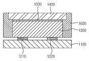
도 1은 본 발명의 일 실시예에 따른 발광 소자 패키지의 단면도.
도 2는 본 발명의 다른 실시예에 따른 발광 소자 패지의 단면도
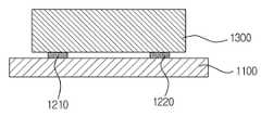
도 3a 내지 도 3d는 도 1의 발광 소자 패키지의 세부 공정을 도시한 단면도.
도 4a 내지 도 4d는 도 2의 발광 소자 패키지의 세부 공정을 도시한 단면도.1 is a cross-sectional view of a light emitting device package according to an embodiment of the present invention;
2 is a cross-sectional view of a light emitting device package according to another embodiment of the present invention
3A to 3D are cross-sectional views illustrating a detailed process of the light emitting device package of FIG.
4A to 4D are cross-sectional views illustrating a detailed process of the light emitting device package of FIG.
이하, 본 발명의 바람직한 실시예를 첨부한 도면을 참조하여 설명하기로 한다.Hereinafter, preferred embodiments of the present invention will be described with reference to the accompanying drawings.
본 발명의 일 실시예에 따른 발광 소자 패키지는 도 1에 도시된 것처럼, 발광 다이오드 소자(1300), 회로 기판(1100), 형광체층(1400), 버퍼층(1500) 및 측부를 포함하여 구성될 수 있다.The light emitting device package according to an embodiment of the present invention may include a light
여기에서, 발광 다이오드 소자(1300)는 소정 영역의 파장의 빛을 제공하며, 구체적으로, 발광 다이오드 소자(1300)는 청색 파장의 빛을 제공하는 발광 다이오드나 자외선 파장의 빛을 제공하는 발광 다이오드일 수 있다.Here, the light
한편, 발광 다이오드 소자(1300)의 하면에는 회로 기판(1100)과 전기적으로 연결되는 본딩 패드(1210, 1220)가 금속 물질로 형성되어 있으며, 이러한 회로 기판(1100)은 발광 다이오드 소자(1300)의 하부에 배치된다.On the other hand,
또한, 형광체층(1400)은 두께가 균일하게 형성되어 발광 다이오드 소자(1300)의 상면에서 발광되는 빛의 파장을 변이시켜 발광 다이오드 소자(1300)가 제공하는 빛을 백색광으로 변환시킨다.여기에서, 형광체층(1400)은 형광체와 실리콘 등에 의해 형성되며, 도 1에 도시된 것처럼, 발광 다이오드 소자(1300)의 상면의 모든 영역을 커버하고도 초과될 수 있도록 배치된다. 상술한 것처럼, 형광체층(1400)이 발광 다이오드 소자(1300)의 상면의 모든 영역을 커버하고도 초과될 수 있도록 배치되면, 발광 다이오드 소자(1300)의 에지 영역에서 발광되는 빛도 백색광으로 변환하여 제공될 수 있으므로, 광 효율이 효과적으로 증가될 수 있다.The
한편, 버퍼층(1500)은 상기 발광 다이오드 소자(1300)의 상면과 상기 형광체층(1400)의 하면 사이에 배치되어, 상기 발광 다이오드 소자(1300)의 상면에서 발생되는 열이 상기 형광체층(1400)의 하면에 전달되는 것을 억제하는 동시에 상기 형광체층(1400)의 하면이 상기 발광 다이오드 소자(1300)의 상면에서 이탈되는 것을 억제한다.The
여기에서, 버퍼층(1500)은 상기 발광 다이오드 소자(1300)의 상면의 일부 또는 전부에만 코팅된 후에 상기 형광체층(1400)이 부착되는 것이 바람직하다.Here, it is preferable that the
또한, 상기 버퍼층(1500)은투명한 실리콘, 투명한 에폭시, 투명한 유기 폴리머, 또는 투명한 글래스 수지 중 적어도 어느 하나를 포함하여 형성되며, 5 ㎛ ~ 150 ㎛ 두께로 형성된다.In addition, the
한편, 측부(1600)는 발광 다이오드 소자(1300)의 측면, 버퍼층(1500)의 측면 및 형광체층(1400)의 측면을 둘러싸도록 배치되어 발광 다이오드 소자(1300)의 측면에서 제공되는 빛을 차단하고 발광 다이오드 소자(1300)의 측면에서 전달되는 열을 외부로 배출하며 버퍼층(1500)의 측면 및 형광체층(1400)의 측면을 보호한다. 여기에서, 측부(1600)는투명한 실리콘, 투명한 에폭시, 투명한 유기 폴리머, 또는 투명한 글래스 수지 중 적어도 어느 하나와, Al2O3, TiO2, Silver 중 적어도 어느 하나의 금속분말을 포함한다.The
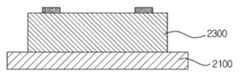
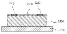
본 발명의 다른 실시예에 따른 발광 소자 패키지는 도 2에 도시된 것처럼, 발광 다이오드 소자(2300), 회로 기판(2100), 형광체층(2400), 버퍼층(2500) 및 측부(2600)를 포함하여 구성될 수 있다.A light emitting device package according to another embodiment of the present invention includes a light
여기에서, 발광 다이오드 소자(2300)는 소정 영역의 파장의 빛을 제공하며, 구체적으로, 발광 다이오드 소자(2300)는 청색 파장의 빛을 제공하는 발광 다이오드나 자외선 파장의 빛을 제공하는 발광 다이오드일 수 있다.Here, the light
한편, 발광 다이오드 소자(2300)의 상면에는 회로 기판(2100)과 전기적으로 연결되는 본딩 패드(2210, 2220)가 금속 물질로 형성되어 있으며, 이러한 회로 기판(2100)은 발광 다이오드 소자(2300)의 하부에 배치된다.On the upper surface of the light
또한, 형광체층(2400)은 두께가 균일하게 형성되어 발광 다이오드 소자(2300)의 상면에서 발광되는 빛의 파장을 변이시켜 발광 다이오드 소자(2300)가 제공하는 빛을 백색광으로 변환시킨다.여기에서, 형광체층(2400)은 형광체와 실리콘 등에 의해 형성된다.The
이러한 형광체층(2400)은 도 2에 도시된 것처럼, 발광 다이오드 소자(2300)의 본딩 패드(2210, 2220)가 노출되도록 상기 형광체층(2400)의 상부에 본딩홀(2410, 2420)이 형성되어 있으며, 발광 다이오드 소자(2300)의 상면의 모든 영역을 커버하고도 초과될 수 있도록 배치된다. 상술한 것처럼, 형광체층(2400)이 발광 다이오드 소자(2300)의 상면의 모든 영역을 커버하고도 초과될 수 있도록 배치되면, 발광 다이오드 소자(2300)의 에지 영역에서 발광되는 빛도 백색광으로 변환하여 제공될 수 있으므로, 광 효율이 효과적으로 증가될 수 있다.2,
한편, 버퍼층(2500)은 상기 발광 다이오드 소자의 상면과 상기 형광체층의 하면 사이의 상기 본딩 패드가 형성된 영역을 제외한 영역에 배치되어, 상기 발광 다이오드 소자의 상면에서 발생되는 열이 상기 형광체층의 하면에 전달되는 것을 억제하는 동시에 상기 형광체층의 하면이 상기 발광 다이오드 소자의 상면에서 이탈되는 것을 억제한다.On the other hand, the
여기에서, 버퍼층(2500)은 상기 발광 다이오드 소자의 상면의 일부 또는 전부에만 코팅된 후에 상기 형광체층이 부착되는 것이 바람직하다.Here, it is preferable that the phosphor layer is attached after the
또한, 상기 버퍼층(2500)은투명한 실리콘, 투명한 에폭시, 투명한 유기 폴리머, 또는 투명한 글래스 수지 중 적어도 어느 하나를 포함하여 형성되며, 5 ㎛ ~ 150 ㎛ 두께로 형성된다.In addition, the
한편, 측부(2600)는 발광 다이오드 소자(2300)의 측면, 버퍼층(2500)의 측면 및 형광체층(2400)의 측면을 둘러싸도록 배치되어 발광 다이오드 소자(2300)의 측면에서 제공되는 빛을 차단하고 발광 다이오드 소자(2300)의 측면에서 전달되는 열을 외부로 배출하며 버퍼층(2500)의 측면 및 형광체층(2400)의 측면을 보호한다. 여기에서, 측부(2600)는투명한 실리콘, 투명한 에폭시, 투명한 유기 폴리머, 또는 투명한 글래스 수지 중 적어도 어느 하나와, Al2O3, TiO2, Silver 중 적어도 어느 하나의 금속분말을 포함한다.On the other hand, the
이하에서는, 도 3a 내지 도 3d를 참조하여, 본 발명의 일 실시예에 따른 발광 다이오드 패키지의 제조 방법에 대해서 설명한다.Hereinafter, a method for fabricating a light emitting diode package according to an embodiment of the present invention will be described with reference to FIGS. 3A to 3D. FIG.
먼저, 도 3a에 도시된 것처럼, 소정 영역의 파장의 빛을 제공하며, 하면에 본딩 패드(1210, 1220)가 형성되어 있는 발광 다이오드 소자(1300)를, 회로 기판(1100) 위에 마운트한다.First, as shown in FIG. 3A, a light emitting
다음으로, 도 3b에 도시된 것처럼, 상기 발광 다이오드 소자(1300)의 상면에, 상기 발광 다이오드 소자(1300)의 상면에서 발생되는 열이 상부로 전달되는 것을 억제하는 동시에 상기 발광 다이오드 소자(1300)의 상면에서 부착될 부품이 이탈되는 것을 억제하는 버퍼층(1500)을 코팅한다.3B, on the upper surface of the light emitting
다음으로, 도 3c에 도시된 것처럼, 두께가 균일하게 형성된 형광체층(1400)이 버퍼층(1500)의 상면에 발광 다이오드 소자(1300)의 상면의 모든 영역을 커버하고도 초과될 수 있도록 배치되어 부착된다.Next, as shown in FIG. 3C, a
다음으로, 도 3d에 도시된 것처럼, 발광 다이오드 소자(1300)의 측면에서 제공되는 빛을 차단하고 발광 다이오드 소자(1300)의 측면에서 전달되는 열을 외부로 배출하며 버퍼층(1500)의 측면 및 형광체층(1400)의 측면을 보호하는 측부(1600)가 발광 다이오드 소자(1300)의 측면, 버퍼층(1500)의 측면 및 형광체층(1400)의 측면을 둘러싸도록 배치되어 부착된다.Next, as shown in FIG. 3D, the light provided on the side of the light emitting
이하에서는, 도 4a 내지 도 4d를 참조하여, 본 발명의 다른 실시예에 따른 발광 다이오드 패키지의 제조 방법에 대해서 설명한다.Hereinafter, a method of manufacturing a light emitting diode package according to another embodiment of the present invention will be described with reference to FIGS. 4A to 4D. FIG.
먼저, 도 4a에 도시된 것처럼, 소정 영역의 파장의 빛을 제공하며, 상면에 본딩 패드(2210, 2220)가 형성되어 있는 발광 다이오드 소자(2300)를, 회로 기판(2100) 위에 마운트한다.First, as shown in FIG. 4A, a light emitting
다음으로, 도 4b에 도시된 것처럼, 상기 발광 다이오드 소자(2300)의 상면의 상기 본딩 패드(2210, 2220)가 형성된 영역을 제외한 영역에, 상기 발광 다이오드 소자(2300)의 상면에서 발생되는 열이 상부로 전달되는 것을 억제하는 동시에 상기 발광 다이오드 소자(2300)의 상면에 부착될 부품이 이탈되는 것을 억제하는 버퍼층(2500)을 코팅한다.4B, the heat generated from the upper surface of the light emitting
다음으로, 도 4c에 도시된 것처럼, 두께가 균일하게 형성되고, 상기 발광 다이오드 소자(2300)의 본딩 패드가 노출되도록 본딩홀(2410, 2420)이 형성된 형광체층(2400)이 버퍼층(2500)의 상면에 발광 다이오드 소자(2300)의 상면의 모든 영역을 커버하고도 초과될 수 있도록 배치되어 부착된다.4C, a
다음으로, 도 4d에 도시된 것처럼, 발광 다이오드 소자(2300)의 측면에서 제공되는 빛을 차단하고 발광 다이오드 소자(2300)의 측면에서 전달되는 열을 외부로 배출하며 버퍼층(2500)의 측면 및 형광체층(2400)의 측면을 보호하는 측부(2600)가 발광 다이오드 소자(2300)의 측면, 버퍼층(2500)의 측면 및 형광체층(2400)의 측면을 둘러싸도록 배치되어 부착된다.4D, the light provided on the side surface of the light emitting
이상, 본 발명을 본 발명의 원리를 예시하기 위한 바람직한 실시예와 관련하여 설명하고 도시하였지만, 본 발명은 그와 같이 도시되고 설명된 그대로의 구성 및 작용으로 한정되는 것이 아니다. While the present invention has been particularly shown and described with reference to exemplary embodiments thereof, it is to be understood that the invention is not limited to the disclosed exemplary embodiments.
오히려, 첨부된 청구범위의 사상 및 범주를 일탈함이 없이 본 발명에 대한 다수의 변경 및 수정이 가능함을 당업자들은 잘 이해할 수 있을 것이다.
On the contrary, those skilled in the art will appreciate that many modifications and variations of the present invention are possible without departing from the spirit and scope of the appended claims.
따라서, 그러한 모든 적절한 변경 및 수정과 균등물들도 본 발명의 범위에 속하는 것으로 간주되어야 할 것이다.
Accordingly, all such appropriate modifications and changes, and equivalents thereof, should be regarded as within the scope of the present invention.
1100, 2100 : 회로 기판
1210, 1220, 2210, 2220 : 본딩 패드
1300, 2300 : 발광 다이오드 소자
1400, 2400 : 형광체층
1500, 2500 : 버퍼층
1600, 2600 : 측부1100, 2100: circuit board
1210, 1220, 2210, 2220: bonding pads
1300, 2300: Light emitting diode element
1400, 2400: phosphor layer
1500, 2500: buffer layer
1600, 2600: side
Claims (16)
Translated fromKorean상기 발광 다이오드 소자의 하면에 형성되어 있는 본딩 패드를 통해서 상기 발광 다이오드 소자와 전기적으로 연결되는 회로 기판;
상기 발광 다이오드 소자의 상면에 배치되는 버퍼층; 및
상기 버퍼층의 상면에 배치되며, 두께가 균일하게 형성된 형광체층을 포함하며,
상기 버퍼층은 상기 발광 다이오드 소자의 상면에서 발생되는 열이 상기 형광체층의 하면에 전달되는 것을 억제하는 동시에 상기 형광체층의 하면이 상기 발광 다이오드 소자의 상면에서 이탈하는 것을 억제하고,
상기 형광체층은 상기 발광 다이오드 소자의 상면의 모든 영역을 커버하고도 초과될 수 있도록 배치되며,
상기 발광 다이오드 소자의 측면, 상기 버퍼층의 측면 및 상기 형광체층의 측면을 둘러싸도록 배치되어 상기 발광 다이오드 소자의 측면에서 제공되는 빛을 차단하고 상기 발광 다이오드 소자의 측면에서 전달되는 열을 외부로 배출하며 상기 버퍼층의 측면 및 상기 형광체층의 측면을 보호하는 측부를 포함하는 발광 다이오드 패키지.
A light emitting diode element for providing light of a wavelength of a predetermined region;
A circuit board electrically connected to the light emitting diode device through a bonding pad formed on a lower surface of the light emitting diode device;
A buffer layer disposed on an upper surface of the light emitting diode; And
And a phosphor layer disposed on the upper surface of the buffer layer and having a uniform thickness,
The buffer layer suppresses the heat generated from the upper surface of the light emitting diode element from being transmitted to the lower surface of the phosphor layer and suppresses the lower surface of the phosphor layer from being separated from the upper surface of the light emitting diode element,
Wherein the phosphor layer covers and covers all areas of the upper surface of the light emitting diode,
A side surface of the buffer layer and a side surface of the phosphor layer to block light provided on a side surface of the light emitting diode device and to discharge heat transmitted from a side surface of the light emitting diode device to the outside And a side portion that protects a side surface of the buffer layer and a side surface of the phosphor layer.
상기 형광체층은 형광체와 실리콘에 의해 형성된 발광 소자 패키지
The method according to claim 1,
The phosphor layer is formed of a phosphor and a light emitting device package
상기 버퍼층은 투명한 실리콘, 투명한 에폭시, 투명한 유기 폴리머, 또는 투명한 글래스 수지 중 적어도 어느 하나를 포함하는 발광 소자 패키지.
The method according to claim 1,
Wherein the buffer layer comprises at least one of transparent silicon, transparent epoxy, transparent organic polymer, or transparent glass resin.
상기 측부는 투명한 실리콘, 투명한 에폭시, 투명한 유기 폴리머, 또는 투명한 글래스 수지 중 적어도 어느 하나와, Al2O3, TiO2, Silver 중 적어도 어느 하나의 금속분말을 포함하는 발광 소자 패키지.
The method according to claim 1,
Wherein the side portion comprises at least one of transparent silicon, transparent epoxy, transparent organic polymer, or transparent glass resin and at least one metal powder of Al2O3, TiO2, or Silver.
상기 발광 다이오드 소자의 하부에 배치되며 상기 본딩 패드를 통해서 상기 발광 다이오드 소자와 전기적으로 연결되는 회로 기판;
상기 발광 다이오드 소자의 상면의 상기 본딩 패드가 형성된 영역을 제외한 영역에 배치되는 버퍼층; 및
상기 버퍼층의 상면에 배치되며, 두께가 균일하고 상기 본딩 패드가 노출되도록 본딩홀이 형성된 형광체층을 포함하며,
상기 버퍼층은 상기 발광 다이오드 소자의 상면에서 발생되는 열이 상기 형광체층의 하면에 전달되는 것을 억제하는 동시에 상기 형광체층의 하면이 상기 발광 다이오드 소자의 상면에서 이탈하는 것을 억제하고,
상기 형광체층은 상기 발광 다이오드 소자의 상면의 모든 영역을 커버하고도 초과될 수 있도록 배치되며,
상기 발광 다이오드 소자의 측면, 상기 버퍼층의 측면 및 상기 형광체층의 측면을 둘러싸도록 배치되어 상기 발광 다이오드 소자의 측면에서 제공되는 빛을 차단하고 상기 발광 다이오드 소자의 측면에서 전달되는 열을 외부로 배출하며 상기 버퍼층의 측면 및 상기 형광체층의 측면을 보호하는 측부를 포함하는 발광 다이오드 패키지.
A light emitting diode element for providing light of a wavelength in a predetermined region and having a bonding pad formed on an upper surface thereof;
A circuit board disposed below the light emitting diode device and electrically connected to the light emitting diode device through the bonding pad;
A buffer layer disposed on an upper surface of the light emitting diode, the bonding pad being disposed in a region except for a region where the bonding pad is formed; And
And a phosphor layer disposed on the upper surface of the buffer layer and having a uniform thickness and a bonding hole to expose the bonding pad,
The buffer layer suppresses the heat generated from the upper surface of the light emitting diode element from being transmitted to the lower surface of the phosphor layer and suppresses the lower surface of the phosphor layer from being separated from the upper surface of the light emitting diode element,
Wherein the phosphor layer covers and covers all areas of the upper surface of the light emitting diode,
A side surface of the buffer layer and a side surface of the phosphor layer to block light provided on a side surface of the light emitting diode device and to discharge heat transmitted from a side surface of the light emitting diode device to the outside And a side portion that protects a side surface of the buffer layer and a side surface of the phosphor layer.
상기 형광체층은 형광체와 실리콘에 의해 형성된 발광 소자 패키지.
6. The method of claim 5,
Wherein the phosphor layer is formed of a phosphor and silicon.
상기 버퍼층은 투명한 실리콘, 투명한 에폭시, 투명한 유기 폴리머, 또는 투명한 글래스 수지 중 적어도 어느 하나를 포함하는 발광 소자 패키지.
6. The method of claim 5,
Wherein the buffer layer comprises at least one of transparent silicon, transparent epoxy, transparent organic polymer, or transparent glass resin.
상기 측부는 투명한 실리콘, 투명한 에폭시, 투명한 유기 폴리머, 또는 투명한 글래스 수지 중 적어도 어느 하나와, Al2O3, TiO2, Silver 중 적어도 어느 하나의 금속분말을 포함하는 발광 소자 패키지.
6. The method of claim 5,
Wherein the side portion comprises at least one of transparent silicon, transparent epoxy, transparent organic polymer, or transparent glass resin and at least one metal powder of Al2O3, TiO2, or Silver.
상기 발광 다이오드 소자의 상면에, 상기 발광 다이오드 소자의 상면에서 발생되는 열이 상부로 전달되는 것을 억제하는 동시에 상기 발광 다이오드 소자의 상면에서 부착될 부품이 이탈되는 것을 억제하는 버퍼층을 코팅하는 단계;
두께가 균일하게 형성된 형광체층이 상기 버퍼층의 상면에 상기 발광 다이오드 소자의 상면의 모든 영역을 커버하고도 초과될 수 있도록 배치되어 부착되는 단계; 및
상기 발광 다이오드 소자의 측면에서 제공되는 빛을 차단하고 상기 발광 다이오드 소자의 측면에서 전달되는 열을 외부로 배출하며 상기 버퍼층의 측면 및 상기 형광체층의 측면을 보호하는 측부가 상기 발광 다이오드 소자의 측면, 상기 버퍼층의 측면 및 상기 형광체층의 측면을 둘러싸도록 배치되어 부착되는 단계를 포함하는 발광 다이오드 패키지의 제조 방법.
Mounting a light emitting diode device on a circuit board, the light emitting diode device providing light of a wavelength of a predetermined region and having a bonding pad formed on a lower surface thereof;
Coating a buffer layer on an upper surface of the light emitting diode device to suppress transfer of heat generated from an upper surface of the light emitting diode device to an upper portion of the light emitting diode device and to prevent a component to be attached from being detached from the upper surface of the light emitting diode device;
A step of arranging and attaching a phosphor layer having a uniform thickness on the upper surface of the buffer layer so as to cover and exceed the entire area of the upper surface of the light emitting diode element; And
Wherein a side portion of the buffer layer and a side portion protecting the side surface of the phosphor layer are formed on a side surface of the light emitting diode device, And a side surface of the buffer layer and a side surface of the phosphor layer.
상기 형광체층은 형광체와 실리콘에 의해 형성된 발광 소자 패키지.
10. The method of claim 9,
Wherein the phosphor layer is formed of a phosphor and silicon.
상기 버퍼층은 투명한 실리콘, 투명한 에폭시, 투명한 유기 폴리머, 또는 투명한 글래스 수지 중 적어도 어느 하나를 포함하는 발광 소자 패키지의 제조 방법.
10. The method of claim 9,
Wherein the buffer layer comprises at least one of transparent silicon, transparent epoxy, transparent organic polymer, or transparent glass resin.
상기 측부는 투명한 실리콘, 투명한 에폭시, 투명한 유기 폴리머, 또는 투명한 글래스 수지 중 적어도 어느 하나와, Al2O3, TiO2, Silver 중 적어도 어느 하나의 금속분말을 포함하는 발광 소자 패키지의 제조 방법.
10. The method of claim 9,
Wherein the side portion comprises at least one of transparent silicon, transparent epoxy, transparent organic polymer, or transparent glass resin and at least one metal powder of Al2O3, TiO2, or Silver.
상기 발광 다이오드 소자의 상면의 상기 본딩 패드가 형성된 영역을 제외한 영역에, 상기 발광 다이오드 소자의 상면에서 발생되는 열이 상부로 전달되는 것을 억제하는 동시에 상기 발광 다이오드 소자의 상면에 부착될 부품이 이탈되는 것을 억제하는 버퍼층을 코팅하는 단계;
두께가 균일하게 형성되고, 상기 발광 다이오드 소자의 본딩 패드가 노출되도록 본딩홀이 형성된 형광체층이 상기 버퍼층의 상면에 상기 발광 다이오드 소자의 상면의 모든 영역을 커버하고도 초과될 수 있도록 배치되어 부착되는 단계; 및
상기 발광 다이오드 소자의 측면에서 제공되는 빛을 차단하고 상기 발광 다이오드 소자의 측면에서 전달되는 열을 외부로 배출하며 상기 버퍼층의 측면 및 상기 형광체층의 측면을 보호하는 측부가 상기 발광 다이오드 소자의 측면, 상기 버퍼층의 측면 및 상기 형광체층의 측면을 둘러싸도록 배치되어 부착되는 단계를 포함하는 발광 다이오드 패키지의 제조 방법.
Mounting a light emitting diode device on a circuit board, the light emitting diode device providing light of a predetermined wavelength and having a bonding pad on an upper surface thereof;
The heat generated in the upper surface of the light emitting diode device is prevented from being transferred to the upper portion of the upper surface of the light emitting diode device except for the region where the bonding pad is formed and the part to be attached to the upper surface of the light emitting diode device is removed Coating a buffer layer on the substrate;
A phosphor layer formed with a bonding hole such that the bonding pad of the LED device is exposed is disposed on the upper surface of the buffer layer so as to cover and cover all the upper surface of the LED device, step; And
Wherein a side portion of the buffer layer and a side portion protecting the side surface of the phosphor layer are formed on a side surface of the light emitting diode device, And a side surface of the buffer layer and a side surface of the phosphor layer.
상기 형광체층은 형광체와 실리콘에 의해 형성된 발광 소자 패키지.
14. The method of claim 13,
Wherein the phosphor layer is formed of a phosphor and silicon.
상기 버퍼층은 투명한 실리콘, 투명한 에폭시, 투명한 유기 폴리머, 또는 투명한 글래스 수지 중 적어도 어느 하나를 포함하는 발광 소자 패키지의 제조 방법.14. The method of claim 13,
Wherein the buffer layer comprises at least one of transparent silicon, transparent epoxy, transparent organic polymer, or transparent glass resin.
상기 측부는 투명한 실리콘, 투명한 에폭시, 투명한 유기 폴리머, 또는 투명한 글래스 수지 중 적어도 어느 하나와, Al2O3, TiO2, Silver 중 적어도 어느 하나의 금속분말을 포함하는 발광 소자 패키지의 제조 방법.
14. The method of claim 13,
Wherein the side portion comprises at least one of transparent silicon, transparent epoxy, transparent organic polymer, or transparent glass resin and at least one metal powder of Al2O3, TiO2, or Silver.
Priority Applications (2)
| Application Number | Priority Date | Filing Date | Title |
|---|---|---|---|
| KR1020150145860AKR20170045851A (en) | 2015-10-20 | 2015-10-20 | Package for Light Emitting Device and Method for Manufacturing thereof |
| PCT/KR2015/014224WO2017069339A1 (en) | 2015-10-20 | 2015-12-24 | Light-emitting device package and manufacturing method therefor |
Applications Claiming Priority (1)
| Application Number | Priority Date | Filing Date | Title |
|---|---|---|---|
| KR1020150145860AKR20170045851A (en) | 2015-10-20 | 2015-10-20 | Package for Light Emitting Device and Method for Manufacturing thereof |
Publications (1)
| Publication Number | Publication Date |
|---|---|
| KR20170045851Atrue KR20170045851A (en) | 2017-04-28 |
Family
ID=58557572
Family Applications (1)
| Application Number | Title | Priority Date | Filing Date |
|---|---|---|---|
| KR1020150145860ACeasedKR20170045851A (en) | 2015-10-20 | 2015-10-20 | Package for Light Emitting Device and Method for Manufacturing thereof |
Country Status (2)
| Country | Link |
|---|---|
| KR (1) | KR20170045851A (en) |
| WO (1) | WO2017069339A1 (en) |
Cited By (3)
| Publication number | Priority date | Publication date | Assignee | Title |
|---|---|---|---|---|
| USD928733S1 (en)* | 2019-11-15 | 2021-08-24 | Logitech Europe S.A. | Audio device |
| USD956714S1 (en) | 2019-12-27 | 2022-07-05 | Samsung Electronics Co., Ltd. | Audio device |
| USD956715S1 (en) | 2019-12-27 | 2022-07-05 | Samsung Electronics Co., Ltd. | Audio device |
Family Cites Families (5)
| Publication number | Priority date | Publication date | Assignee | Title |
|---|---|---|---|---|
| JP3546650B2 (en)* | 1997-07-28 | 2004-07-28 | 日亜化学工業株式会社 | Method of forming light emitting diode |
| KR20100021891A (en)* | 2008-08-18 | 2010-02-26 | 삼성전기주식회사 | Semiconductor chip package and manufacturing method thereof |
| KR101562022B1 (en)* | 2009-02-02 | 2015-10-21 | 삼성디스플레이 주식회사 | Light emitting diode unit display device having the same and manufacturing mathod of the light emitting diode unit |
| KR101752426B1 (en)* | 2010-12-03 | 2017-07-11 | 서울반도체 주식회사 | Light emitting device and light emitting diode package |
| JP2015095588A (en)* | 2013-11-13 | 2015-05-18 | シチズンホールディングス株式会社 | Led package |
- 2015
- 2015-10-20KRKR1020150145860Apatent/KR20170045851A/ennot_activeCeased
- 2015-12-24WOPCT/KR2015/014224patent/WO2017069339A1/ennot_activeCeased
Cited By (3)
| Publication number | Priority date | Publication date | Assignee | Title |
|---|---|---|---|---|
| USD928733S1 (en)* | 2019-11-15 | 2021-08-24 | Logitech Europe S.A. | Audio device |
| USD956714S1 (en) | 2019-12-27 | 2022-07-05 | Samsung Electronics Co., Ltd. | Audio device |
| USD956715S1 (en) | 2019-12-27 | 2022-07-05 | Samsung Electronics Co., Ltd. | Audio device |
Also Published As
| Publication number | Publication date |
|---|---|
| WO2017069339A1 (en) | 2017-04-27 |
Similar Documents
| Publication | Publication Date | Title |
|---|---|---|
| US9496465B2 (en) | Light emitting device | |
| JP6186904B2 (en) | Light emitting device | |
| CN102214774B (en) | Light emitting device package and light unit having the same | |
| CN103403894B (en) | Light emitting module, lamp, illumination apparatus and display device | |
| CN103797597B (en) | Light emitting module, lamp, luminaire and display device | |
| US8545082B2 (en) | Light emitting apparatus and lighting system | |
| US20130009183A1 (en) | Reflective circuit board for led backlight | |
| KR20160138814A (en) | Light emitting device and vehicle lamp comprising the same | |
| TW200723566A (en) | Light emitting diode package with metal reflective layer and method of manufacturing the same | |
| WO2011084001A2 (en) | Aspheric led lens and a light emitting device including the same | |
| JP6485503B2 (en) | Method for manufacturing light emitting device | |
| KR20170045851A (en) | Package for Light Emitting Device and Method for Manufacturing thereof | |
| US8878208B2 (en) | Illuminating device | |
| KR20150122360A (en) | Package for Light Emitting Device and Method for Manufacturing thereof | |
| KR101212654B1 (en) | Package for light emitting diode and method for manufacturing thereof | |
| KR20110125066A (en) | Light emitting device package | |
| KR20170003182A (en) | Light emitting diode | |
| KR101081170B1 (en) | Light emitting device packag and method for fabricating thereof | |
| KR20150092597A (en) | Light emitting device package and lighting apparatus including the same | |
| KR20170043839A (en) | Package for Light Emitting Device and Method for Manufacturing thereof | |
| KR101616474B1 (en) | Package for Light Emitting Device and Method for Manufacturing thereof | |
| KR20150136041A (en) | Package for Light Emitting Device and Method for Manufacturing thereof | |
| TW201538893A (en) | Color temperature adjustment method of light-emitting device | |
| KR20140098523A (en) | Light-emitting device | |
| KR102142718B1 (en) | Light emitting device and light apparatus having thereof |
Legal Events
| Date | Code | Title | Description |
|---|---|---|---|
| A201 | Request for examination | ||
| PA0109 | Patent application | Patent event code:PA01091R01D Comment text:Patent Application Patent event date:20151020 | |
| PA0201 | Request for examination | ||
| E902 | Notification of reason for refusal | ||
| PE0902 | Notice of grounds for rejection | Comment text:Notification of reason for refusal Patent event date:20161018 Patent event code:PE09021S01D | |
| AMND | Amendment | ||
| E601 | Decision to refuse application | ||
| PE0601 | Decision on rejection of patent | Patent event date:20170419 Comment text:Decision to Refuse Application Patent event code:PE06012S01D Patent event date:20161018 Comment text:Notification of reason for refusal Patent event code:PE06011S01I | |
| PG1501 | Laying open of application | ||
| AMND | Amendment | ||
| PX0901 | Re-examination | Patent event code:PX09011S01I Patent event date:20170419 Comment text:Decision to Refuse Application Patent event code:PX09012R01I Patent event date:20161215 Comment text:Amendment to Specification, etc. | |
| PX0601 | Decision of rejection after re-examination | Comment text:Decision to Refuse Application Patent event code:PX06014S01D Patent event date:20170531 Comment text:Amendment to Specification, etc. Patent event code:PX06012R01I Patent event date:20170518 Comment text:Decision to Refuse Application Patent event code:PX06011S01I Patent event date:20170419 Comment text:Amendment to Specification, etc. Patent event code:PX06012R01I Patent event date:20161215 Comment text:Notification of reason for refusal Patent event code:PX06013S01I Patent event date:20161018 |