KR20170045806A - Semiconductor memory device and method of operating the same - Google Patents
Semiconductor memory device and method of operating the sameDownload PDFInfo
- Publication number
- KR20170045806A KR20170045806AKR1020150145731AKR20150145731AKR20170045806AKR 20170045806 AKR20170045806 AKR 20170045806AKR 1020150145731 AKR1020150145731 AKR 1020150145731AKR 20150145731 AKR20150145731 AKR 20150145731AKR 20170045806 AKR20170045806 AKR 20170045806A
- Authority
- KR
- South Korea
- Prior art keywords
- data
- unit
- sub
- command
- page
- Prior art date
- Legal status (The legal status is an assumption and is not a legal conclusion. Google has not performed a legal analysis and makes no representation as to the accuracy of the status listed.)
- Withdrawn
Links
Images


Classifications
- G—PHYSICS
- G06—COMPUTING OR CALCULATING; COUNTING
- G06F—ELECTRIC DIGITAL DATA PROCESSING
- G06F3/00—Input arrangements for transferring data to be processed into a form capable of being handled by the computer; Output arrangements for transferring data from processing unit to output unit, e.g. interface arrangements
- G06F3/06—Digital input from, or digital output to, record carriers, e.g. RAID, emulated record carriers or networked record carriers
- G06F3/0601—Interfaces specially adapted for storage systems
- G06F3/0668—Interfaces specially adapted for storage systems adopting a particular infrastructure
- G06F3/0671—In-line storage system
- G06F3/0673—Single storage device
- G06F3/0679—Non-volatile semiconductor memory device, e.g. flash memory, one time programmable memory [OTP]
- G—PHYSICS
- G11—INFORMATION STORAGE
- G11C—STATIC STORES
- G11C29/00—Checking stores for correct operation ; Subsequent repair; Testing stores during standby or offline operation
- G11C29/04—Detection or location of defective memory elements, e.g. cell constructio details, timing of test signals
- G11C29/08—Functional testing, e.g. testing during refresh, power-on self testing [POST] or distributed testing
- G11C29/12—Built-in arrangements for testing, e.g. built-in self testing [BIST] or interconnection details
- G11C29/38—Response verification devices
- G11C29/42—Response verification devices using error correcting codes [ECC] or parity check
- G—PHYSICS
- G11—INFORMATION STORAGE
- G11C—STATIC STORES
- G11C29/00—Checking stores for correct operation ; Subsequent repair; Testing stores during standby or offline operation
- G11C29/52—Protection of memory contents; Detection of errors in memory contents
- G—PHYSICS
- G06—COMPUTING OR CALCULATING; COUNTING
- G06F—ELECTRIC DIGITAL DATA PROCESSING
- G06F11/00—Error detection; Error correction; Monitoring
- G06F11/07—Responding to the occurrence of a fault, e.g. fault tolerance
- G06F11/08—Error detection or correction by redundancy in data representation, e.g. by using checking codes
- G06F11/10—Adding special bits or symbols to the coded information, e.g. parity check, casting out 9's or 11's
- G06F11/1008—Adding special bits or symbols to the coded information, e.g. parity check, casting out 9's or 11's in individual solid state devices
- G06F11/1048—Adding special bits or symbols to the coded information, e.g. parity check, casting out 9's or 11's in individual solid state devices using arrangements adapted for a specific error detection or correction feature
- G06F11/106—Correcting systematically all correctable errors, i.e. scrubbing
- G—PHYSICS
- G06—COMPUTING OR CALCULATING; COUNTING
- G06F—ELECTRIC DIGITAL DATA PROCESSING
- G06F3/00—Input arrangements for transferring data to be processed into a form capable of being handled by the computer; Output arrangements for transferring data from processing unit to output unit, e.g. interface arrangements
- G06F3/06—Digital input from, or digital output to, record carriers, e.g. RAID, emulated record carriers or networked record carriers
- G06F3/0601—Interfaces specially adapted for storage systems
- G06F3/0602—Interfaces specially adapted for storage systems specifically adapted to achieve a particular effect
- G06F3/0614—Improving the reliability of storage systems
- G06F3/0619—Improving the reliability of storage systems in relation to data integrity, e.g. data losses, bit errors
- G—PHYSICS
- G06—COMPUTING OR CALCULATING; COUNTING
- G06F—ELECTRIC DIGITAL DATA PROCESSING
- G06F3/00—Input arrangements for transferring data to be processed into a form capable of being handled by the computer; Output arrangements for transferring data from processing unit to output unit, e.g. interface arrangements
- G06F3/06—Digital input from, or digital output to, record carriers, e.g. RAID, emulated record carriers or networked record carriers
- G06F3/0601—Interfaces specially adapted for storage systems
- G06F3/0628—Interfaces specially adapted for storage systems making use of a particular technique
- G06F3/0638—Organizing or formatting or addressing of data
- G06F3/064—Management of blocks
- G—PHYSICS
- G11—INFORMATION STORAGE
- G11C—STATIC STORES
- G11C16/00—Erasable programmable read-only memories
- G11C16/02—Erasable programmable read-only memories electrically programmable
- G11C16/06—Auxiliary circuits, e.g. for writing into memory
- G—PHYSICS
- G11—INFORMATION STORAGE
- G11C—STATIC STORES
- G11C29/00—Checking stores for correct operation ; Subsequent repair; Testing stores during standby or offline operation
- G11C29/70—Masking faults in memories by using spares or by reconfiguring
- G11C29/78—Masking faults in memories by using spares or by reconfiguring using programmable devices
- G11C29/783—Masking faults in memories by using spares or by reconfiguring using programmable devices with refresh of replacement cells, e.g. in DRAMs
- G—PHYSICS
- G11—INFORMATION STORAGE
- G11C—STATIC STORES
- G11C11/00—Digital stores characterised by the use of particular electric or magnetic storage elements; Storage elements therefor
- G11C11/02—Digital stores characterised by the use of particular electric or magnetic storage elements; Storage elements therefor using magnetic elements
- G11C11/16—Digital stores characterised by the use of particular electric or magnetic storage elements; Storage elements therefor using magnetic elements using elements in which the storage effect is based on magnetic spin effect
- G11C11/165—Auxiliary circuits
- G11C11/1673—Reading or sensing circuits or methods
- G—PHYSICS
- G11—INFORMATION STORAGE
- G11C—STATIC STORES
- G11C11/00—Digital stores characterised by the use of particular electric or magnetic storage elements; Storage elements therefor
- G11C11/02—Digital stores characterised by the use of particular electric or magnetic storage elements; Storage elements therefor using magnetic elements
- G11C11/16—Digital stores characterised by the use of particular electric or magnetic storage elements; Storage elements therefor using magnetic elements using elements in which the storage effect is based on magnetic spin effect
- G11C11/165—Auxiliary circuits
- G11C11/1675—Writing or programming circuits or methods
Landscapes
- Engineering & Computer Science (AREA)
- Theoretical Computer Science (AREA)
- Physics & Mathematics (AREA)
- General Engineering & Computer Science (AREA)
- General Physics & Mathematics (AREA)
- Human Computer Interaction (AREA)
- Quality & Reliability (AREA)
- Computer Security & Cryptography (AREA)
- For Increasing The Reliability Of Semiconductor Memories (AREA)
- Computer Hardware Design (AREA)
Abstract
Translated fromKorean
Description
Translated fromKorean본 발명은 메모리 분야에 관한 것으로, 보다 상세하게는 반도체 메모리 장치 및 반도체 메모리 장치의 동작 방법에 관한 것이다.The present invention relates to a memory field, and more particularly, to a semiconductor memory device and a method of operating the semiconductor memory device.
반도체 메모리 장치는 플래시 메모리 장치와 같은 불휘발성 메모리 장치와 DRAM과 같은 휘발성 메모리 장치로 구분될 수 있다. DRAM과 같은 휘발성 메모리 장치는 가격이 비교적 저렴하기 때문에 시스템 메모리와 같은 대용량 데이터를 저장하는데 사용되고 있다. 또한 DRAM과 같은 휘발성 반도체 메모리 장치에서는 집적도를 높이기 위하여 공정 스케일을 축소시키고 있다. 공정 스케일의 축소에 따라 비트 에러 비율(bit error rate)을 급격하게 증가하고 수율이 낮아질 것으로 예상된다.The semiconductor memory device may be classified into a nonvolatile memory device such as a flash memory device and a volatile memory device such as a DRAM. Volatile memory devices such as DRAMs are being used to store large amounts of data, such as system memory, because they are relatively inexpensive. In addition, in a volatile semiconductor memory device such as a DRAM, the process scale is reduced in order to increase the degree of integration. It is expected that the bit error rate will increase sharply and the yield will decrease as the process scale decreases.
본 발명의 일 목적은 성능을 높이면서 전력 소모를 감소시킬 수 있는 반도체 메모리 장치를 제공하는 것이다.It is an object of the present invention to provide a semiconductor memory device capable of reducing power consumption while improving performance.
본 발명의 일 목적은 성능을 높이면서 전력 소모를 감소시킬 수 있는 반도체 메모리 장치의 동작 방법을 제공하는 것이다.It is an object of the present invention to provide a method of operating a semiconductor memory device capable of reducing power consumption while increasing performance.
상기 일 목적을 달성하기 위한 본 발명의 일 실시예에 따른 메모리 셀 어레이와 에러 정정 회로를 구비하는 반도체 메모리 장치의 동작 방법에서는 외부의 메모리 컨트롤러로부터 수신된 제1 커맨드에 응답하여 상기 메모리 셀 어레이의 하나의 페이지의 적어도 하나의 서브 페이지를 선택하고, 상기 서브 페이지로부터 적어도 두 개의 서브 유닛들 및 패리티 데이터를 구비하는 제1 유닛의 데이터를 독출하고, 상기 독출된 제1 유닛의 데이터에 대하여 에러를 존재하는지 여부를 판단하고, 상기 독출된 제1 유닛의 데이터에 에러가 존재하는 경우, 상기 제1 유닛의 데이터 중 패리티 데이터를 이용하여 상기 에러를 포함하는 서브 유닛의 데이터를 정정하고, 상기 정정된 서브 유닛을 상기 서브 페이지에 재기입한다.According to an embodiment of the present invention, there is provided an operation method of a semiconductor memory device including a memory cell array and an error correction circuit, including the steps of: receiving a first command from an external memory controller; Selecting at least one subpage of one page, reading data of a first unit having at least two sub-units and parity data from the sub-page, and generating an error for the data of the read first unit Corrects the data of the sub-unit including the error by using the parity data of the data of the first unit, if there is an error in the data of the read first unit, The sub-unit is rewritten in the sub-page.
예시적인 실시예에 있어서, 상기 동작 방법에서는 상기 외부의 메모리 컨트롤러로부터 제2 커맨드를 수신할 수 있다.In an exemplary embodiment, the operating method may receive a second command from the external memory controller.
예시적인 실시예에 있어서, 상기 제1 유닛은 상기 반도체 메모리 장치의 코드워드 단위에 해당하고, 상기 서브 유닛은 상기 반도체 메모리 장치의 프리페치(pre-fetch) 단위에 해당할 수 있다.In an exemplary embodiment, the first unit corresponds to a code word unit of the semiconductor memory device, and the sub-unit corresponds to a pre-fetch unit of the semiconductor memory device.
예시적인 실시예에 있어서, 상기 에러가 존재하는지 여부를 판단하는 것은, 상기 에러 정정 회로에서 상기 독출된 제1 유닛의 데이터에 기초하여 신드롬 데이터를 생성하여 수행될 수 있다.In an exemplary embodiment, determining whether or not the error exists may be performed by generating syndrome data based on the data of the first unit read out in the error correction circuit.
예시적인 실시예에 있어서, 상기 제1 커맨드는 상기 반도체 메모리 장치의 독출 동작을 위한 독출 커맨드와 서로 다른 신호 조합으로 구성되는 스크러빙 커맨드일 수 있다.In an exemplary embodiment, the first command may be a scrubbing command composed of a read command for a read operation of the semiconductor memory device and a different signal combination.
상기 메모리 셀 어레이는 복수의 뱅크 어레이들을 포함하고, 상기 뱅크 어레이들 각각은 복수의 페이지들을 구비하고, 각각의 페이지는 복수의 서브 페이지들을 포함할 수 있다. 상기 제1 커맨드에 의하여 하나의 페이지가 활성화되고, 활성화된 페이지의 적어도 두 개의 서브 페이지에 대하여 정정된 서브 유닛이 재기입될 수 있다.The memory cell array includes a plurality of bank arrays, each of the bank arrays having a plurality of pages, and each page may include a plurality of sub pages. One page is activated by the first command and the corrected subunit can be rewritten for at least two subpages of the activated page.
예시적인 실시예에 있어서, 상기 제1 커맨드는 일정한 주기에 따라 수신되고, 상기 메모리 셀 어레이는 복수의 뱅크 어레이들을 포함하고, 상기 뱅크 어레이들 각각은 복수의 페이지들을 구비할 수 있다. 상기 복수의 페이지들은 상기 제1 커맨드가 수신됨에 따라 순차적으로 활성화되고, 상기 활성화된 하나의 페이지의 복수의 서브 페이지들이 순차적으로 선택될 수 있다.In an exemplary embodiment, the first command is received in a predetermined period, the memory cell array includes a plurality of bank arrays, and each of the bank arrays may have a plurality of pages. The plurality of pages are sequentially activated as the first command is received, and a plurality of sub pages of the activated one page may be sequentially selected.
예시적인 실시예에 있어서, 상기 제1 커맨드는 상기 반도체 메모리 장치의 리프레쉬 동작을 위한 리프레쉬 커맨드일 수 있다.In an exemplary embodiment, the first command may be a refresh command for a refresh operation of the semiconductor memory device.
상기 메모리 셀 어레이는 복수의 뱅크 어레이들을 포함하고, 상기 뱅크 어레이들 각각은 복수의 페이지들을 구비할 수 있다. 상기 리프레쉬 커맨드에 응답하여 어느 하나의 페이지가 활성화되고, 활성화된 페이지의 하나의 서브 페이지에 대하여 정정된 서브 유닛이 재기입될 수 있다.The memory cell array includes a plurality of bank arrays, and each of the bank arrays may include a plurality of pages. One of the pages is activated in response to the refresh command, and the corrected sub-unit can be rewritten to one sub-page of the activated page.
상기 일 목적을 달성하기 위한 본 발명의 일 실시예에 따른 메모리 셀 어레이와 에러 정정 회로를 구비하는 반도체 메모리 장치의 동작 방법에서는, 부의 메모리 컨트롤러로부터 수신된 제1 커맨드에 응답하여 상기 메모리 셀 어레이의 하나의 페이지의 적어도 하나의 서브 페이지를 선택하고, 상기 서브 페이지로부터 적어도 두 개의 서브 유닛들 및 패리티 데이터를 구비하는 제1 유닛의 데이터를 독출하고, 상기 독출된 제1 유닛의 데이터에 대하여 에러를 존재하는지 여부를 판단하고, 상기 독출된 제1 유닛의 데이터에 에러가 존재하는 경우, 상기 제1 유닛의 데이터 중 상기 패리티 데이터를 이용하여 상기 에러를 포함하는 서브 유닛의 데이터를 정정하고, 기입 데이터 및 상기 정정된 서브 유닛의 데이터에 기초하여 기입 패리티 데이터를 생성하고, 상기 기입 데이터 및 상기 패리티 데이터를 적어도 포함하는 수정된 코드워드를 상기 서브 페이지에 기입한다.According to an aspect of the present invention, there is provided a method of operating a semiconductor memory device including a memory cell array and an error correction circuit, the method comprising: Selecting at least one subpage of one page, reading data of a first unit having at least two sub-units and parity data from the sub-page, and generating an error for the data of the read first unit Corrects the data of the subunit including the error by using the parity data among the data of the first unit when there is an error in the data of the read first unit, And generating write parity data based on the data of the corrected sub-unit, And writes the modified code word including at least the write data and the parity data in the sub page.
예시적인 실시예에 있어서, 상기 동작 방법은 상기 외부의 메모리 컨트롤러로부터 제2 커맨드를 더 수신할 수 있다.In an exemplary embodiment, the operating method may further receive a second command from the external memory controller.
예시적인 실시예에 있어서, 상기 제1 유닛은 상기 반도체 메모리 장치의 코드워드 단위에 해당하고, 상기 서브 유닛과 상기 기입 데이터의 크기는 상기 반도체 메모리 장치의 프리페치(pre-fetch) 단위에 해당할 수 있다.In an exemplary embodiment, the first unit corresponds to a code word unit of the semiconductor memory device, and the size of the sub-unit and the write data corresponds to a pre-fetch unit of the semiconductor memory device .
예시적인 실시예에 있어서, 상기 서브 페이지에서 상기 정정된 서브 유닛의 데이터가 기입될 위치와 상기 기입 데이터가 기입될 위치가 다른 경우에, 상기 기입 데이터, 상기 정정된 서브 유닛의 데이터 및 상기 기입 패리티 데이터가 상기 수정된 코드워드로서 상기 서브 페이지에 기입될 수 있다.In the exemplary embodiment, when the position at which the data of the corrected sub-unit is to be written and the position at which the write data is to be written in the sub page are different, the write data, the data of the corrected sub- Data may be written to the subpage as the modified codeword.
예시적인 실시예에 있어서, 상기 서브 페이지에서 상기 정정된 서브 유닛의 데이터가 기입될 위치와 상기 기입 데이터가 기입될 위치가 동일한 경우에, 상기 기입 데이터 및 상기 기입 패리티 데이터가 상기 수정된 코드워드로서 상기 서브 페이지에 기입될 수 있다.In the exemplary embodiment, when the position at which the data of the corrected sub-unit is to be written and the position at which the write data is to be written in the sub-page are the same, the write data and the write parity data are written as the modified code word And can be written in the sub page.
예시적인 실시예에 있어서, 상기 에러가 존재하는지 여부를 판단하는 것은, 상기 에러 정정 회로에서 상기 독출된 제1 유닛의 데이터에 기초하여 신드롬 데이터를 생성하여 수행될 수 있다.In an exemplary embodiment, determining whether or not the error exists may be performed by generating syndrome data based on the data of the first unit read out in the error correction circuit.
예시적인 실시예에 있어서, 상기 제1 커맨드는 상기 반도체 메모리 장치의 기입 동작을 위한 기입 커맨드일 수 있다.In an exemplary embodiment, the first command may be a write command for a write operation of the semiconductor memory device.
상기 메모리 셀 어레이는 복수의 뱅크 어레이들을 포함하고, 상기 뱅크 어레이들 각각은 복수의 페이지들을 구비하고, 상기 제1 커맨드에 의하여 어느 하나의 페이지가 선택되고, 상기 선택된 페이지의 복수의 서브 페이지들이 순차적으로 활성화될 수 있다.Wherein the memory cell array includes a plurality of bank arrays, each of the bank arrays has a plurality of pages, one of the pages is selected by the first command, a plurality of sub pages of the selected page are sequentially Lt; / RTI >
상기 일 목적을 달성하기 위한 본 발명의 일 실시예에 따른 반도체 메모리 장치는 메모리 셀 어레이, 제어 로직 회로 및 에러 정정 회로를 포함한다. 상기 메모리 셀 어레이는 복수의 페이지들을 각각 구비하는 복수의 뱅크 어레이들을 포함한다. 상기 제어 로직 회로는 외부의 메모리 컨트롤러로부터의 커맨드를 디코딩하여 제어 신호들을 생성한다. 상기 에러 정정 회로는 상기 메모리 셀 어레이로부터의 독출 데이터에 대하여 에러 정정 코드(error correction code; 'ECC') 디코딩을 수행한다. 상기 제어 로직 회로는 상기 메모리 컨트롤러로부터 수신된 제1 커맨드에 응답하여 상기 복수의 페이지들 중 하나의 페이지의 적어도 하나의 서브 페이지를 선택하고, 상기 서브 페이지로부터 적어도 두 개의 서브 유닛들 및 패리티 데이터를 구비하는 제1 유닛의 데이터를 독출하여, 에러를 포함하는 서브 유닛의 데이터가 상기 서브 페이지에 재기입되도록 상기 에러 정정 회로를 제어한다.According to an aspect of the present invention, there is provided a semiconductor memory device including a memory cell array, a control logic circuit, and an error correction circuit. The memory cell array includes a plurality of bank arrays each having a plurality of pages. The control logic circuit decodes a command from an external memory controller to generate control signals. The error correction circuit performs error correction code (ECC) decoding on the read data from the memory cell array. Wherein the control logic circuit is responsive to a first command received from the memory controller to select at least one subpage of one page of the plurality of pages and to receive at least two subunits and parity data from the subpage Reads the data of the first unit and controls the error correction circuit so that the data of the sub unit including the error is rewritten in the sub page.
예시적인 실시예에 있어서, 상기 제1 유닛은 상기 반도체 메모리 장치의 코드워드 단위에 해당하고, 상기 서브 유닛은 상기 반도체 메모리 장치의 프리페치(pre-fetch) 단위에 해당할 수 있다.In an exemplary embodiment, the first unit corresponds to a code word unit of the semiconductor memory device, and the sub-unit corresponds to a pre-fetch unit of the semiconductor memory device.
예시적인 실시예에 있어서, 상기 메모리 셀 어레이는 3차원 메모리 셀 어레이이고, 상기 뱅크 어레이들 각각은 복수의 동적 메모리 셀들 또는 복수의 저항성 메모리 셀들을 포함할 수 있다.In an exemplary embodiment, the memory cell array is a three-dimensional memory cell array, and each of the bank arrays may comprise a plurality of dynamic memory cells or a plurality of resistive memory cells.
본 발명의 예시적인 실시예들에 따르면, 반도체 메모리 장치와 이의 동작 방법에서는 스크러빙 모드에서 코드워드의 에러를 정정하고, 에러가 정정된 서브 유닛의 데이터만을 서브 페이지에 재기입함으로써 전력 소모를 감소시킬 수 있다.According to exemplary embodiments of the present invention, in a semiconductor memory device and an operation method thereof, an error of a code word is corrected in a scrubbing mode, and power consumption is reduced by rewriting data of an error corrected sub-unit in a sub- .
도 1은 본 발명의 실시예들에 따른 전자 시스템을 나타내는 블록도이다.
도 2는 본 발명의 실시예들에 따른 도 1의 메모리 시스템의 개략적인 구성을 나타내는 블록도이다.
도 3은 본 발명의 실시예들에 따른 도 2의 반도체 메모리 장치의 구성을 나타내는 블록도이다.
도 4a 내지 도 4e는 도 3에 도시된 메모리 셀을 예시적으로 나타내는 회로도들이다.
도 5는 본 발명의 실시예들에 따른 도 3의 반도체 메모리 장치에서 메모리 셀의 예를 나타낸다.
도 6a 및 도 6b는 도 5의 MTJ 소자의 기입된 데이터에 따른 자화 방향을 나타낸다.
도 7은 스크러빙 모드에서 도 3의 반도체 메모리 장치의 일부를 나타낸다.
도 8은 기입 동작에서 도 3의 반도체 메모리 장치의 일부를 나타낸다.
도 9는 도 3의 반도체 메모리 장치의 하나의 뱅크 어레이와 에러 정정 회로를 나타낸다.
도 10은 스크러빙 모드에서 도 3의 반도체 메모리 장치에서 에러 정정 회로와 입출력 게이팅 회로를 나타낸다.
도 11은 독출 동작과 기입 동작시의 3의 반도체 메모리 장치에서 에러 정정 회로와 입출력 게이팅 회로를 나타낸다.
도 12는 도 7의 반도체 메모리 장치에서 스크러빙 동작이 수행되는 것을 나타낸다.
도 13은 도 8의 반도체 메모리 장치에서 기입 동작이 수행되는 것을 나타낸다.
도 14는 도 8의 반도체 메모리 장치에서 기입 동작이 수행되는 것을 나타낸다.
도 15는 도 10의 에러 정정 회로에서 ECC 인코더를 나타낸다.
도 16은 도 10의 에러 정정 회로에서 ECC 디코더를 나타낸다.
도 17은 본 발명의 실시예들에 따른 반도체 메모리 장치의 동작 방법을 나타내는 흐름도이다.
도 18은 본 발명의 실시예들에 따른 반도체 메모리 장치의 동작 방법을 나타내는 흐름도이다.
도 19는 본 발명의 실시예들에 따른 반도체 메모리 장치를 나타내는 구조도이다.
도 20은 본 발명의 실시예에 따른 반도체 메모리 장치가 적용된 메모리 시스템 나타내는 블록도이다.
도 21은 본 발명의 실시예들에 따른 반도체 메모리 장치를 컴퓨팅 시스템에 응용한 예를 나타내는 블록도이다.1 is a block diagram illustrating an electronic system according to embodiments of the present invention.
Figure 2 is a block diagram illustrating a schematic configuration of the memory system of Figure 1 in accordance with embodiments of the present invention.
3 is a block diagram showing the configuration of the semiconductor memory device of FIG. 2 according to the embodiments of the present invention.
4A to 4E are circuit diagrams exemplarily showing the memory cell shown in FIG.
Figure 5 shows an example of a memory cell in the semiconductor memory device of Figure 3 according to embodiments of the present invention.
6A and 6B show the magnetization directions according to the written data of the MTJ element of FIG.
Fig. 7 shows a part of the semiconductor memory device of Fig. 3 in the scrubbing mode.
Fig. 8 shows a part of the semiconductor memory device of Fig. 3 in the write operation.
9 shows one bank array and error correction circuit of the semiconductor memory device of FIG.
10 shows an error correction circuit and an input / output gating circuit in the semiconductor memory device of FIG. 3 in the scrubbing mode.
11 shows an error correction circuit and an input / output gating circuit in the semiconductor memory device of the third example in the read operation and the write operation.
12 shows that the scrubbing operation is performed in the semiconductor memory device of Fig.
13 shows that a write operation is performed in the semiconductor memory device of Fig.
14 shows that a write operation is performed in the semiconductor memory device of Fig.
15 shows an ECC encoder in the error correction circuit of Fig.
16 shows an ECC decoder in the error correction circuit of Fig.
17 is a flowchart showing a method of operating a semiconductor memory device according to embodiments of the present invention.
18 is a flowchart showing an operation method of the semiconductor memory device according to the embodiments of the present invention.
19 is a structural diagram showing a semiconductor memory device according to embodiments of the present invention.
20 is a block diagram showing a memory system to which a semiconductor memory device according to an embodiment of the present invention is applied.
21 is a block diagram showing an example of application of a semiconductor memory device according to embodiments of the present invention to a computing system.
본문에 개시되어 있는 본 발명의 실시예들에 대해서, 특정한 구조적 내지 기능적 설명들은 단지 본 발명의 실시예를 설명하기 위한 목적으로 예시된 것으로, 본 발명의 실시예들은 다양한 형태로 실시될 수 있으며 본문에 설명된 실시예들에 한정되는 것으로 해석되어서는 아니 된다.For the embodiments of the invention disclosed herein, specific structural and functional descriptions are set forth for the purpose of describing an embodiment of the invention only, and it is to be understood that the embodiments of the invention may be practiced in various forms, The present invention should not be construed as limited to the embodiments described in Figs.
본 발명은 다양한 변경을 가할 수 있고 여러 가지 형태를 가질 수 있는 바, 특정 실시예들을 도면에 예시하고 본문에 상세하게 설명하고자 한다. 그러나, 이는 본 발명을 특정한 개시 형태에 대해 한정하려는 것이 아니며, 본 발명의 사상 및 기술 범위에 포함되는 모든 변경, 균등물 내지 대체물을 포함하는 것으로 이해되어야 한다. 각 도면을 설명하면서 유사한 참조부호를 구성요소에 대해 사용하였다.The present invention is capable of various modifications and various forms, and specific embodiments are illustrated in the drawings and described in detail in the text. It should be understood, however, that the invention is not intended to be limited to the particular forms disclosed, but includes all modifications, equivalents, and alternatives falling within the spirit and scope of the invention. Similar reference numerals have been used for the components in describing each drawing.
제1, 제2 등의 용어는 다양한 구성요소들을 설명하는데 사용될 수 있지만, 상기 구성요소들은 상기 용어들에 의해 한정되어서는 안된다. 상기 용어들은 하나의 구성요소를 다른 구성요소로부터 구별하는 목적으로만 사용된다. 예를 들어, 본 발명의 권리 범위로부터 이탈되지 않은 채 제1 구성요소는 제2 구성요소로 명명될 수 있고, 유사하게 제2 구성요소도 제1 구성요소로 명명될 수 있다.The terms first, second, etc. may be used to describe various elements, but the elements should not be limited by the terms. The terms are used only for the purpose of distinguishing one component from another. For example, without departing from the scope of the present invention, the first component may be referred to as a second component, and similarly, the second component may also be referred to as a first component.
어떤 구성요소가 다른 구성요소에 "연결되어" 있다거나 "접속되어" 있다고 언급된 때에는, 그 다른 구성요소에 직접적으로 연결되어 있거나 또는 접속되어 있을 수도 있지만, 중간에 다른 구성요소가 존재할 수도 있다고 이해되어야 할 것이다. 반면에, 어떤 구성요소가 다른 구성요소에 "직접 연결되어" 있다거나 "직접 접속되어" 있다고 언급된 때에는, 중간에 다른 구성요소가 존재하지 않는 것으로 이해되어야 할 것이다. 구성요소들 간의 관계를 설명하는 다른 표현들, 즉 "~사이에"와 "바로 ~사이에" 또는 "~에 이웃하는"과 "~에 직접 이웃하는" 등도 마찬가지로 해석되어야 한다.It is to be understood that when an element is referred to as being "connected" or "connected" to another element, it may be directly connected or connected to the other element, . On the other hand, when an element is referred to as being "directly connected" or "directly connected" to another element, it should be understood that there are no other elements in between. Other expressions that describe the relationship between components, such as "between" and "between" or "neighboring to" and "directly adjacent to" should be interpreted as well.
본 출원에서 사용한 용어는 단지 특정한 실시예를 설명하기 위해 사용된 것으로, 본 발명을 한정하려는 의도가 아니다. 단수의 표현은 문맥상 명백하게 다르게 뜻하지 않는 한, 복수의 표현을 포함한다. 본 출원에서, "포함하다" 또는 "가지다" 등의 용어는 설시된 특징, 숫자, 단계, 동작, 구성요소, 부분품 또는 이들을 조합한 것이 존재함을 지정하려는 것이지, 하나 또는 그 이상의 다른 특징들이나 숫자, 단계, 동작, 구성요소, 부분품 또는 이들을 조합한 것들의 존재 또는 부가 가능성을 미리 배제하지 않는 것으로 이해되어야 한다.The terminology used in this application is used only to describe a specific embodiment and is not intended to limit the invention. The singular expressions include plural expressions unless the context clearly dictates otherwise. In the present application, the terms "comprise", "having", and the like are intended to specify the presence of stated features, integers, steps, operations, elements, components, or combinations thereof, , Steps, operations, components, parts, or combinations thereof, as a matter of principle.
다르게 정의되지 않는 한, 기술적이거나 과학적인 용어를 포함해서 여기서 사용되는 모든 용어들은 본 발명이 속하는 기술 분야에서 통상의 지식을 가진 자에 의해 일반적으로 이해되는 것과 동일한 의미를 가지고 있다. 일반적으로 사용되는 사전에 정의되어 있는 것과 같은 용어들은 관련 기술의 문맥 상 가지는 의미와 일치하는 의미를 가지는 것으로 해석되어야 하며, 본 출원에서 명백하게 정의하지 않는 한, 이상적이거나 과도하게 형식적인 의미로 해석되지 않는다.Unless defined otherwise, all terms used herein, including technical or scientific terms, have the same meaning as commonly understood by one of ordinary skill in the art to which this invention belongs. Terms such as those defined in commonly used dictionaries are to be interpreted as having a meaning consistent with the contextual meaning of the related art and are to be interpreted as either ideal or overly formal in the sense of the present application Do not.
이하, 첨부한 도면들을 참조하여, 본 발명의 바람직한 실시예를 보다 상세하게 설명하고자 한다. 도면상의 동일한 구성요소에 대해서는 동일한 참조부호를 사용하고 동일한 구성요소에 대해서 중복된 설명은 생략한다.Hereinafter, preferred embodiments of the present invention will be described in detail with reference to the accompanying drawings. The same reference numerals are used for the same constituent elements in the drawings and redundant explanations for the same constituent elements are omitted.
도 1은 본 발명의 실시예들에 따른 전자 시스템을 나타내는 블록도이다.1 is a block diagram illustrating an electronic system according to embodiments of the present invention.
도 1을 참조하면, 전자 시스템(또는, 전자 장치, 10)은 호스트(15) 및 메모리 시스템(20)을 포함할 수 있다. 메모리 시스템(20)은 메모리 컨트롤러(100) 및 복수의 반도체 메모리 장치들(200a~200n)을 포함할 수 있다.Referring to FIG. 1, an electronic system (or electronic device) 10 may include a
호스트(15)는 PCI-E(Peripheral Component Interconnect - Express), ATA(Advanced Technology Attachment), SATA(Serial ATA), PATA(Parallel ATA), 또는 SAS(serial attached SCSI)와 같은 인터페이스 프로토콜을 사용하여 메모리 시스템(20)과 통신할 수 있다. 또한 호스트(15)와 메모리 시스템(20)간의 인터페이스 프로토콜들은 상술한 예에 한정되지 않으며, USB(Universal Serial Bus), MMC(Multi-Media Card), ESDI(Enhanced Small Disk Interface), 또는 IDE(Integrated Drive Electronics) 등과 같은 다른 인터페이스 프로토콜들 중 하나일 수 있다.The
메모리 컨트롤러(Memory Controller; 100)는 메모리 시스템(Memory System; 20)의 동작을 전반적으로 제어하며, 호스트(15)와 메모리 장치들(200a~200n) 사이의 전반적인 데이터 교환을 제어한다. 예컨대, 메모리 컨트롤러(100)는 호스트(15)의 요청에 따라 반도체 메모리 장치들(200a~200n)을 제어하여 데이터를 기입하거나(write) 데이터를 독출한다(read).A
또한, 메모리 컨트롤러(100)는 반도체 메모리 장치들(200a~200n)을 제어하기 위한 동작 커맨드(command)들을 인가하여, 반도체 메모리 장치들(200a~200n)의 동작을 제어한다.In addition, the
실시예에 따라, 반도체 메모리 장치들(200a~200n) 각각은 저항성 메모리 셀들을 구비하는 PRAM(Phase change Random Access Memory), RRAM(Resistive Random Access Memory), MRAM(Magnetic Random Access Memory) 및 FRAM(Ferroelectric Random Access Memory) 중 하나일 일 수 있다. 다른 실시예에서, 반도체 메모리 장치들(200a~200n) 각각은 동적 메모리 셀들을 구비하는 DRAM(dynamic random access) 일 수 있다.Each of the
MRAM은 자기저항(magnetoresistance) 기반의 비휘발성 컴퓨터 메모리 기술이다. MRAM은 여러가지 면에서 휘발성 RAM과 다르다. MRAM은 비휘발성이기 때문에, 메모리 장치 전원이 오프되어도 MRAM은 메모리 내용을 유지할 수 있다.MRAM is a nonvolatile computer memory technology based on magnetoresistance. MRAM differs from volatile RAM in many ways. Since the MRAM is non-volatile, the MRAM can maintain the memory contents even when the memory device is powered off.
일반적으로 비휘발성 RAM이 휘발성 RAM 보다 느리다고 하지만, MRAM은 휘발성 RAM의 독출 및 기입 응답 시간들에 견줄만한 독출 및 기입 응답 시간을 갖는다. 전하로서 데이터를 저장하는 전형적인 RAM 기술과는 달리, MRAM 데이터는 자기저항 요소들에 의해 데이터를 저장한다. 일반적으로, 자기저항 요소들은 2개 자성층들로 이루어지고, 각 자성층은 자화(magnetization)를 가진다.Generally, non-volatile RAM is slower than volatile RAM, but MRAM has read and write response times comparable to volatile RAM read and write response times. Unlike a typical RAM technology for storing data as a charge, MRAM data stores data by magnetoresistive elements. Generally, the magnetoresistive elements are composed of two magnetic layers, and each magnetic layer has magnetization.
MRAM은 두 개의 자성층과 그 사이에 개재된 절연막을 포함하는 자기 터널 접합 패턴(magnetic tunnel junction pattern)을 사용하여 데이터를 읽고 쓰는 불휘발성 메모리 장치이다. 자성층의 자화 방향에 따라 자기 터널 접합 패턴의 저항값이 달라질 수 있는데, 이러한 저항값의 차이를 이용하여 데이터를 프로그래밍 또는 제거할 수 있다.An MRAM is a nonvolatile memory device that reads and writes data using a magnetic tunnel junction pattern including two magnetic layers and an insulating film interposed therebetween. The resistance value of the magnetic tunnel junction pattern may vary depending on the magnetization direction of the magnetic layer. Data can be programmed or removed using the difference in resistance value.
스핀 전달 토크(spin transfer torque: STT) 현상을 이용한 MRAM은 한쪽 방향으로 스핀(spin)이 분극화(polarized)된 전류를 흘려줄 때, 전자의 스핀 전달에 의해 자성층의 자화 방향이 달라지는 방식을 이용한다. 하나의 자성층(고정 층, pinned layer)의 자화 방향이 고정되고, 다른 하나의 자성층(자유 층, free layer)은 프로그램 전류에 의해 발생되는 자기장에 의해 자화 방향이 변할 수 있다.An MRAM using a spin transfer torque (STT) phenomenon uses a method in which a magnetization direction of a magnetic layer is changed by spin transfer of electrons when a spinned polarized current flows in one direction. The magnetization direction of one magnetic layer (pinned layer) is fixed and the magnetization direction of the other magnetic layer (free layer) can be changed by the magnetic field generated by the program current.
프로그램 전류의 자기장은 두 자성층의 자화 방향을 평행(parallel) 하거나 반-평행(anti-parallel) 하게 배열할 수 있다. 자화 방향이 평행하면, 두 자성층들 사이의 저항이 낮은 로우("0") 상태를 나타낸다. 자화 방향이 반-평행하면, 두 자성층들 사이의 저항이 높은 하이("1") 상태를 나타낸다. 자유 층의 자화 방향 스위칭과 그 결과 자성층들 사이의 하이 또는 로우 저항 상태는 MRAM의 기입 및 독출 동작을 제공한다.The magnetic field of the program current can align the magnetization directions of the two magnetic layers in parallel or anti-parallel. When the magnetization directions are parallel, the resistance between the two magnetic layers shows a low ("0") state. When the magnetization direction is anti-parallel, the resistance between the two magnetic layers exhibits a high ("1") state. The magnetization direction switching of the free layer and consequently the high or low resistance state between the magnetic layers provides write and read operations of the MRAM.
MRAM 기술이 비휘발성과 빠른 응답 시간을 제공하지만, MRAM 셀은 스케일링 한계에 부딪히고 기입 디스터번스(disturbance)에 민감하다. MRAM 자성층들 사이의 하이와 로우 저항 상태를 스위칭하기 위하여 인가되는 프로그램 전류는 전형적으로 높다(high). 이에 따라, MRAM 어레이 내 다수개의 셀들이 배열될 때, 하나의 메모리 셀로 인가되는 프로그램 전류는 인접한 셀의 자유 층의 필드 변화를 유발한다. 이러한 기입 디스터번스 문제는 STT 현상을 이용하여 해결할 수 있다. 전형적인 STT-MRAM(Spin Transfer Torque Magnetoresistive Random Access Memory)은 자기 터널 접합(magnetic tunnel junction, MTJ) 소자를 포함할 수 있다. MTJ 소자는 2개의 자성층들(고정 층, 자유 층)과 자성층들 사이의 절연층을 포함하는 자기 저항 데이터 저장 소자이다.While MRAM technology provides non-volatility and fast response time, MRAM cells are subject to scaling limits and are susceptible to write disturbance. The program current applied to switch the high and low resistance states between the MRAM magnetic layers is typically high. Thus, when a plurality of cells in an MRAM array are arranged, a program current applied to one memory cell causes a field change of a free layer of an adjacent cell. The problem of the write disturbance can be solved by using the STT phenomenon. A typical STT-MRAM (Spin Transfer Torque Magnetoresistive Random Access Memory) may include a magnetic tunnel junction (MTJ) device. The MTJ element is a magnetoresistive data storage element including two magnetic layers (a fixed layer, a free layer) and an insulating layer between the magnetic layers.
프로그램 전류는 전형적으로 MTJ 소자를 통해 흐른다. 고정 층은 프로그램 전류의 전자 스핀을 분극화하고, 스핀-분극된 전자 전류가 MTJ를 통과함에 따라 토크가 생성된다. 스핀-분극된 전자 전류는 자유 층에 토크를 가하면서 자유 층과 상호 작용한다. MTJ 소자를 통과하는 스핀-분극화된 전자 전류의 토크가 임계 스위칭 전류 밀도보다 크면, 스핀-분극된 전자 전류에 의해 가해지는 토크는 자유 층의 자화 방향을 스위치하기에 충분하다. 이에 따라, 자유 층의 자화 방향은 고정층에 대하여 평행 또는 반-평행으로 배열할 수 있고, MTJ 사이의 저항 상태가 변화된다.The program current typically flows through the MTJ element. The pinned layer polarizes the electron spin of the program current, and a torque is generated as the spin-polarized electron current passes through the MTJ. The spin-polarized electron current interacts with the free layer while applying a torque to the free layer. If the torque of the spin-polarized electron current passing through the MTJ element is greater than the threshold switching current density, the torque applied by the spin-polarized electron current is sufficient to switch the magnetization direction of the free layer. Accordingly, the magnetization direction of the free layer can be arranged parallel or anti-parallel to the fixed layer, and the resistance state between the MTJs is changed.
STT-MRAM은, 스핀-분극된 전자 전류가 자기 저항 소자 내 자유 층을 스위치하기 위한 외부 자기장의 필요를 없애주는 특징을 갖는다. 게다가, 셀 사이즈 감소와 함께 프로그램 전류 감소에 따라 스케일링이 향상되고, 기입 디스터번스 문제를 해결한다. 추가적으로, STT-MRAM은 높은 터널 자기 저항 비가 가능하고, 하이와 로우 저항 상태들 사이의 높은 비를 허용하여, 자기 도메인(magnetic domain) 내 독출 동작을 향상시킨다.The STT-MRAM has a feature in which the spin-polarized electron current eliminates the need for an external magnetic field for switching the free layer in the magnetoresistive element. In addition, scaling improves with program current reduction with cell size reduction, solving the write disturbance problem. In addition, the STT-MRAM allows a high tunneling magnetoresistance ratio and allows a high ratio between high and low resistance states, thereby improving read operation in the magnetic domain.
MRAM은 DRAM (Dynamic Random Access Memory)의 저비용, 고용량 특성과 SRAM (Static Random Access Memory)의 고속 동작 특성, 그리고 플래쉬 메모리(Fresh Memory)의 불휘발성 특성을 모두 갖는 메모리 장치이다.MRAM is a memory device having both low cost and high capacity characteristics of DRAM (Dynamic Random Access Memory), high-speed operation characteristics of SRAM (Static Random Access Memory), and non-volatile characteristics of flash memory.
도 2는 본 발명의 실시예들에 따른 도 1의 메모리 시스템의 개략적인 구성을 나타내는 블록도이다.Figure 2 is a block diagram illustrating a schematic configuration of the memory system of Figure 1 in accordance with embodiments of the present invention.
도 2에서는 메모리 컨트롤러(100)에 대응되는 하나의 반도체 메모리 장치(200a)만을 예로 들어 설명한다.In FIG. 2, only one
도 2를 참조하면, 메모리 시스템(20)은 메모리 컨트롤러(100)와 반도체 메모리 장치(200a)를 포함할 수 있다. 메모리 컨트롤러(100)와 반도체 메모리 장치(200a)는 각각 대응하는 커맨드 핀(101, 201), 어드레스 핀(102, 202), 데이터 핀(103, 203) 및 별도의 핀(104, 204)을 통하여 서로 연결될 수 있다. 커맨드 핀(101, 201)들은 커맨드 전송선(TL1)을 통하여 커맨드 신호(CMD)를 전송하고, 어드레스 핀들(102, 202)은 어드레스 전송선(TL2)을 통하여 어드레스 신호(ADDR)를 전송하고, 데이터 핀들(103, 203)은 데이터 전송선(TL3)을 통하여 메인 데이터(MD)를 교환하고, 별도의 핀들(104, 204)은 전송선(TL4)을 통하여 데이터 마스크 신호(DM)를 전송할 수 있다. 후술되는 바와 같이, 반도체 메모리 장치(200a)는 마스크 신호(DM)에 응답하여 마스크된 기입 동작을 수행할 수 있다. 실시예에 있어서, 별도의 핀들(104, 204)과 전송선(TL4)은 메모리 시스템(20)에 포함되지 않을 수도 있다.Referring to FIG. 2, the
반도체 메모리 장치(200a)는 메인 데이터(MD)가 저장되는 메모리 셀 어레이(300), 에러 정정 회로(400) 및 에러 정정 회로(400)를 제어하는 제어 로직 회로(또는 제어 로직, 210)를 포함할 수 있다.The
반도체 메모리 장치(200a)는 커맨드 신호(CMD)가 스크러빙 커맨드인 경우에, 메모리 셀 어레이(300)의 하나의 페이지를 활성화시키고, 활성화된 페이지의 복수의 서브 페이지들 중 하나를 선택하고, 선택된 서브 페이지로부터 제1 유닛의 데이터를 독출할 수 있다. 여기서 제1 유닛의 데이터는 적어도 두 개의 서브 유닛의 데이터 및 패리티 데이터를 포함할 수 있다. 반도체 메모리 장치(200a)는 패리티 데이터를 이용하여 제1 유닛의 데이터 중 에러를 포함하는 서브 유닛의 데이터를 정정하고, 정정된 서브 유닛의 데이터를 상기 서브 페이지에 재기입(write-back)하는 스크러빙(scrubbing) 동작을 수행할 수 있다.The
반도체 메모리 장치(200a)는 커맨드 신호(CMD)가 반도체 메모리 장치(200a)를 리프레쉬하기 위한 리프레쉬 커맨드인 경우에도 리프레쉬 동작을 수행하면서 상술한 스크러빙 동작을 수행할 수 있다.The
여기서 제1 유닛의 데이터의 크기는 반도체 메모리 장치(200a)의 코드워드의 크기에 해당할 수 있고, 서브 유닛의 데이터의 크기는 반도체 메모리 장치(200a)의 기입 및 독출 동작시에 프리페치(pre-fetch)되는 데이터의 크기에 해당할 수 있다.Here, the size of the data of the first unit may correspond to the size of the code word of the
도 3은 본 발명의 실시예들에 따른 도 2의 반도체 메모리 장치의 구성을 나타내는 블록도이다.3 is a block diagram showing the configuration of the semiconductor memory device of FIG. 2 according to the embodiments of the present invention.
도 3을 참조하면, 반도체 메모리 장치(200a)는 제어 로직 회로(210), 어드레스 레지스터(220), 뱅크 제어 로직(230), 리프레쉬 카운터(297), 로우 어드레스 멀티플렉서(240), 컬럼 어드레스 래치(250), 로우 디코더(260), 컬럼 디코더(270), 메모리 셀 어레이(300), 센스 앰프부(285), 입출력 게이팅 회로(290), 에러 정정 회로(400) 및 데이터 입출력 버퍼(299)를 포함할 수 있다.3, the
실시예에 따라서, 리프레쉬 카운터(297)는 반도체 메모리 장치(200a)에 포함되지 않을 수도 있다. 즉 메모리 셀 어레이(300)가 복수의 저항성 메모리 셀들로 구현되는 경우, 리프레쉬 카운터(297)는 반도체 메모리 장치(200a)에 포함되지 않을 수도 있다.According to the embodiment, the
상기 메모리 셀 어레이(300)는 제1 내지 제4 뱅크 어레이들(310~340)을 포함할 수 있다. 또한, 상기 로우 디코더(260)는 제1 내지 제4 뱅크 어레이들(310~340)에 각각 연결된 제1 내지 제4 뱅크 로우 디코더들(260a~260d)을 포함하고, 상기 컬럼 디코더(270)는 제1 내지 제4 뱅크 어레이들(310~340)에 각각 연결된 제1 내지 제4 뱅크 컬럼 디코더들(270a~270d)을 포함하며, 상기 센스 앰프부(285)는 제1 내지 제4 뱅크 어레이들(310~340)에 각각 연결된 제1 내지 제4 뱅크 센스 앰프들(285a~285d)을 포함할 수 있다. 제1 내지 제4 뱅크 어레이들(310~340), 제1 내지 제4 뱅크 센스 앰프들(285a~2854), 제1 내지 제4 뱅크 칼럼 디코더들(270a~270d) 및 제1 내지 제4 뱅크 로우 디코더들(260a~260d)은 제1 내지 제4 뱅크들을 각각 구성할 수 있다. 제1 내지 제4 뱅크 어레이들(310~340) 각각은 복수의 워드라인(WL)들과 복수의 비트라인(BTL)들 및 워드라인(WL)들과 비트라인(BTL)들이 교차하는 지점에 형성되는 복수의 메모리 셀(MC)들을 포함할 수 있다. 도 3에는 4개의 뱅크들을 포함하는 반도체 메모리 장치(200a)의 예가 도시되어 있으나, 실시예에 따라, 반도체 메모리 장치(200a)는 임의의 수의 뱅크들을 포함할 수 있다.The
어드레스 레지스터(220)는 메모리 컨트롤러(100)로부터 뱅크 어드레스(BANK_ADDR), 로우 어드레스(ROW_ADDR) 및 컬럼 어드레스(COL_ADDR)를 포함하는 어드레스(ADDR)를 수신할 수 있다. 어드레스 레지스터(220)는 수신된 뱅크 어드레스(BANK_ADDR)를 뱅크 제어 로직(230)에 제공하고, 수신된 로우 어드레스(ROW_ADDR)를 로우 어드레스 멀티플렉서(240)에 제공하며, 수신된 컬럼 어드레스(COL_ADDR)를 컬럼 어드레스 래치(250)에 제공할 수 있다.The
뱅크 제어 로직(230)은 뱅크 어드레스(BANK_ADDR)에 응답하여 뱅크 제어 신호들을 생성할 수 있다. 상기 뱅크 제어 신호들에 응답하여, 제1 내지 제4 뱅크 로우 디코더들(260a~260d) 중 뱅크 어드레스(BANK_ADDR)에 상응하는 뱅크 로우 디코더가 활성화되고, 제1 내지 제4 뱅크 컬럼 디코더들(270a~270d) 중 뱅크 어드레스(BANK_ADDR)에 상응하는 뱅크 컬럼 디코더가 활성화될 수 있다.The
리프레쉬 카운터(297)는 제어 로직 회로(210)로부터의 제어에 따라 메모리 셀 어레이(300)에 포함되는 메모리 셀 로우들을 리프레쉬하기 위한 리프레쉬 로우 어드레스(REF_ADDR)를 생성할 수 있다. 리프레쉬 카운터(297)는 메모리 셀 어레이(300)의 메모리 셀(MC)들이 동적 메모리 셀들로 구성되는 경우에 반도체 메모리 장치(200a)에 포함될 수 있다.The
로우 어드레스 멀티플렉서(240)는 어드레스 레지스터(220)로부터 로우 어드레스(ROW_ADDR)를 수신하고, 리프레쉬 카운터(297)로부터 리프레쉬 로우 어드레스(REF_ADDR)를 수신할 수 있다. 로우 어드레스 멀티플렉서(240)는 로우 어드레스(ROW_ADDR) 또는 리프레쉬 로우 어드레스(REF_ADDR)를 로우 어드레스(RA)로서 선택적으로 출력할 수 있다. 로우 어드레스 멀티플렉서(245)로부터 출력된 로우 어드레스(RA)는 제1 내지 제4 뱅크 로우 디코더들(260a~260d)에 각각 인가될 수 있다.The
제1 내지 제4 뱅크 로우 디코더들(260a~260d) 중 뱅크 제어 로직(230)에 의해 활성화된 뱅크 로우 디코더는 로우 어드레스 멀티플렉서(240)로부터 출력된 로우 어드레스(RA)를 디코딩하여 상기 로우 어드레스에 상응하는 워드 라인을 활성화할 수 있다. 예를 들어, 상기 활성화된 뱅크 로우 디코더는 로우 어드레스에 상응하는 워드 라인에 워드 라인 구동 전압을 인가할 수 있다.The bank row decoder activated by the
컬럼 어드레스 래치(250)는 어드레스 레지스터(220)로부터 컬럼 어드레스(COL_ADDR)를 수신하고, 수신된 컬럼 어드레스(COL_ADDR)를 일시적으로 저장할 수 있다. 또한, 컬럼 어드레스 래치(250)는, 버스트 모드에서, 수신된 컬럼 어드레스(COL_ADDR)를 점진적으로 증가시킬 수 있다. 컬럼 어드레스 래치(250)는 일시적으로 저장된 또는 점진적으로 증가된 컬럼 어드레스(COL_ADDR)를 제1 내지 제4 뱅크 컬럼 디코더들(270a~270d)에 각각 인가할 수 있다.The
제1 내지 제4 뱅크 컬럼 디코더들(270a~270d) 중 뱅크 제어 로직(230)에 의해 활성화된 뱅크 컬럼 디코더는 입출력 게이팅 회로(290)를 통하여 뱅크 어드레스(BANK_ADDR) 및 컬럼 어드레스(COL_ADDR)에 상응하는 센스 앰프를 활성화시킬 수 있다.The bank column decoder activated by the
입출력 게이팅 회로(290)는 입출력 데이터를 게이팅하는 회로들과 함께, 입력 데이터 마스크 로직, 제1 내지 제4 뱅크 어레이들(310~340)로부터 출력된 데이터를 저장하기 위한 독출 데이터 래치들, 및 제1 내지 제4 뱅크 어레이들(310~340)에 데이터를 기입하기 위한 기입 드라이버들을 포함할 수 있다.The input /
제1 내지 제4 뱅크 어레이들(310~340) 중 하나의 뱅크 어레이에서 독출될 데이터는 상기 하나의 뱅크 어레이에 상응하는 센스 앰프에 의해 감지되고, 상기 독출 데이터 래치들에 저장될 수 있다. 제1 내지 제4 뱅크 어레이들(310~340) 중 하나의 뱅크 어레이에 기입될 메인 데이터(MD)는 상기 메모리 컨트롤러(100)로부터 데이터 입출력 버퍼(299)에 제공될 수 있다. 데이터 입출력 버퍼(299)에 제공된 메인 데이터(MD)는 에러 정정 회로(400)에서 코드워드(CW)로 인코딩되어 입출력 게이팅 회로(290)에 제공된다. 코드워드(CW)는 상기 기입 드라이버들을 통하여 상기 하나의 뱅크 어레이에 기입될 수 있다.Data to be read out from one of the bank arrays of the first to
데이터 입출력 버퍼(299)는 기입 동작에서는 메모리 컨트롤러(100)로부터 제공되는 메인 데이터(MD)를 에러 정정 회로(400)에 제공하고, 독출 동작에서는 에러 정정 회로(400)로부터 제공되는 메인 데이터(MD)를 메모리 컨트롤러(100)에 제공할 수 있다.The data input /
에러 정정 회로(400)는 기입 동작에서 데이터 입출력 버퍼(299)로부터 제공되는 메인 데이터(MD)에 기초하여 패리티 데이터를 생성하고, 메인 데이터(MD)와 패리티 데이터를 포함하는 코드워드(CW)를 입출력 게이팅 회로(290)에 제공하고, 입출력 게이팅 회로(290)는 코드워드(CW)를 뱅크 어레이에 기입할 수 있다.The
또한 에러 정정 회로(400)는 독출 동작에서 하나의 뱅크 어레이에서 독출된 코드워드(CW)를 입출력 게이팅 회로(290)로부터 제공받을 수 있다. 에러 정정 회로(400)는 독출된 코드워드(CW)에 포함되는 패리티 데이터를 메인 데이터(MD)에 대한 디코딩을 수행하여 메인 데이터(MD)에 포함되는 싱글 비트 에러를 정정하여 데이터 입출력 버퍼(299)에 제공할 수 있다.In addition, the
또한 에러 정정 회로(400)는 스크러빙 동작에서 활성화된 페이지의 복수의 서브 페이지들 중 선택된 하나의 서브 페이지로부터 독출된 제1 유닛의 데이터 중 패리티 데이터를 이용하여 제1 유닛의 데이터 중 에러를 포함하는 서브 유닛의 데이터를 정정하고, 정정된 서브 유닛의 데이터를 상기 서브 페이지에 재기입(write-back)하는 스크러빙 동작을 수행할 수 있다.In addition, the
제어 로직 회로(210)는 반도체 메모리 장치(200a)의 동작을 제어할 수 있다. 예를 들어, 제어 로직 회로(210)는 반도체 메모리 장치(200a)가 기입 동작 또는 독출 동작을 수행하도록 제어 신호들을 생성할 수 있다. 제어 로직 회로(210)은 상기 메모리 컨트롤러(100)로부터 수신되는 커맨드(CMD)를 디코딩하는 커맨드 디코더(211) 및 반도체 메모리 장치(200a)의 동작 모드를 설정하기 위한 모드 레지스터(212)를 포함할 수 있다.The
예를 들어, 커맨드 디코더(211)는 기입 인에이블 신호(/WE), 로우 어드레스 스트로브 신호(/RAS), 컬럼 어드레스 스트로브 신호(/CAS), 칩 선택 신호(/CS) 등을 디코딩하여 커맨드(CMD)에 상응하는 상기 제어 신호들을 생성할 수 있다. 특히 제어 로직 회로(210)는 커맨드(CMD)를 디코딩하여 입출력 게이팅 회로(290)를 제어하는 제1 제어 신호(CTL1)와 에러 정정 회로(400)를 제2 제어 신호(CTL2)를 생성할 수 있다.For example, the
제어 로직 회로(210)는 커맨드(CMD)가 스크러빙 동작을 지시하는 스크러빙 커맨드인 경우에, 입출력 게이팅 회로(290)와 에러 정정 회로(400)가 상술한 스크러빙 동작을 수행하도록 제1 제어 신호(CTL1)와 제2 제어 신호(CTL2)를 생성할 수 있다.The
커맨드(CMD)가 스크러빙 커맨드인 경우에, 스크러빙 커맨드는 반도체 메모리 장치(200a)의 독출 동작을 위한 독출 커맨드와는 서로 다른 신호 조합으로 구성될 수 있다.When the command CMD is a scrubbing command, the scrubbing command may be composed of a signal combination different from a read command for a read operation of the
도 4a 내지 도 4e는 도 3에 도시된 메모리 셀을 예시적으로 나타내는 회로도들이다.4A to 4E are circuit diagrams exemplarily showing the memory cell shown in FIG.
도 4a 내지 도 4d에서는 도 3의 메모리 셀(MC)이 저항성 메모리 셀로 구현된 경우를 나타내고, 도 4e는 도 3의 메모리 셀(MC)이 동적 메모리 셀로 구현된 경우를 나타낸다.4A to 4D show a case where the memory cell MC of FIG. 3 is implemented as a resistive memory cell, and FIG. 4E shows a case where the memory cell MC of FIG. 3 is implemented as a dynamic memory cell.
도 4a는 선택 소자가 없는 저항성 메모리 셀을 나타낸다. 도 4b 내지 도 4d는 선택 소자를 포함하는 저항성 메모리 셀을 나타낸다.Figure 4A shows a resistive memory cell without a selection element. Figures 4B-4D show a resistive memory cell comprising a selection device.
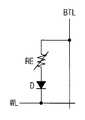
도 4a를 참조하면, 메모리 셀(MC)은 비트 라인(BTL) 및 워드 라인(WL)에 연결되는 저항성 소자(RE)를 포함한다. 이처럼 선택 소자가 없는 구조를 갖는 저항성 메모리 셀은 비트 라인(BTL)과 워드 라인(WL) 사이에 인가되는 전압에 의해서 데이터를 저장한다.Referring to FIG. 4A, a memory cell MC includes a resistive element RE connected to a bit line BTL and a word line WL. The resistive memory cell having such a structure without a selection element stores data by a voltage applied between the bit line BTL and the word line WL.
도 4b를 참조하면, 메모리 셀(MC)은 저항성 소자(RE)와 다이오드(D)를 포함한다. 저항성 소자(RE)는 데이터를 저장하기 위한 저항성 물질을 포함한다. 다이오드(D)는 워드 라인(WL) 및 비트 라인(BTL)의 바이어스에 따라 저항성 소자(RE)에 전류를 공급 또는 차단하는 선택 소자(또는, 스위칭 소자)이다. 다이오드(D)는 저항성 소자(RE)와 워드 라인(WL) 사이에 연결되며, 저항성 소자(RE)는 비트 라인(BTL)과 다이오드(D) 사이에 연결된다. 다이오드(D)와 저항성 소자(RE)의 위치는 서로 바뀔 수 있다. 다이오드(D)는 워드 라인(WL) 전압에 의해 턴온 또는 턴오프 된다. 따라서, 비선택된 워드 라인(WL)에 일정 레벨 이상의 전압을 제공하면, 저항성 메모리 셀은 구동되지 않는다.Referring to FIG. 4B, the memory cell MC includes a resistive element RE and a diode D. The resistive element RE includes a resistive material for storing data. The diode D is a selection element (or a switching element) that supplies or cuts off the current to the resistive element RE according to the bias of the word line WL and the bit line BTL. The diode D is connected between the resistive element RE and the word line WL and the resistive element RE is connected between the bit line BTL and the diode D. The positions of the diode D and the resistive element RE may be changed from each other. Diode D is turned on or off by the word line (WL) voltage. Therefore, when a voltage higher than a certain level is supplied to the unselected word line WL, the resistive memory cell is not driven.
도 4c를 참조하면, 메모리 셀(MC)은 저항성 소자(RE)와 양방향 다이오드(BD)를 포함한다. 저항성 소자(RE)는 데이터를 저장하기 위한 저항성 물질을 포함한다. 양방향 다이오드(BD)는 저항성 소자(RE)와 워드 라인(WL) 사이에 연결되며, 저항성 소자(RE)는 비트 라인(BTL)과 양방향 다이오드(BD) 사이에 연결된다. 양방향 다이오드(BD)와 저항성 소자(RE)의 위치는 서로 바뀔 수 있다. 양방향 다이오드(BD)는 비선택 저항성 메모리 셀에 흐르게 되는 누설 전류를 차단할 수 있다.Referring to FIG. 4C, the memory cell MC includes a resistive element RE and a bi-directional diode BD. The resistive element RE includes a resistive material for storing data. The bidirectional diode BD is connected between the resistive element RE and the word line WL and the resistive element RE is connected between the bit line BTL and the bidirectional diode BD. The positions of the bidirectional diode BD and the resistive element RE may be mutually changed. The bidirectional diode BD can block the leakage current flowing in the non-selective resistive memory cell.
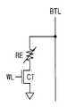
도 4d를 참조하면, 메모리 셀(MC)은 저항성 소자(RE)와 트랜지스터(CT)를 포함한다. 트랜지스터(CT)는 워드 라인(WL)의 전압에 따라 저항성 소자(RE)에 전류를 공급 또는 차단하는 선택 소자(또는, 스위칭 소자)이다. 트랜지스터(CT)는 저항성 소자(RE)와 워드 라인(WL) 사이에 연결되며, 저항성 소자(R)는 비트 라인(BTL)과 트랜지스터(CT) 사이에 연결된다. 트랜지스터(CT)와 저항성 소자(RE)의 위치는 서로 바뀔 수 있다. 메모리 셀(MC)은 워드 라인(WL)에 의해서 구동되는 트랜지스터(CT)의 온-오프 여부에 따라 선택 또는 비선택될 수 있다.Referring to FIG. 4D, the memory cell MC includes a resistive element RE and a transistor CT. The transistor CT is a selection element (or a switching element) that supplies or cuts off the current to the resistive element RE according to the voltage of the word line WL. The transistor CT is connected between the resistive element RE and the word line WL and the resistive element R is connected between the bit line BTL and the transistor CT. The positions of the transistor CT and the resistive element RE may be switched from each other. The memory cell MC may be selected or unselected depending on whether the transistor CT driven by the word line WL is turned on or off.
도 4e를 참조하면, 메모리 셀(MC)은 셀 커패시터(CC)와 트랜지스터(CT)를 포함한다. 트랜지스터(CT)는 워드 라인(WL)의 전압에 따라 셀 커패시터(CC)를 비트라인에 연결 또는 차단하는 선택 소자이다. 트랜지스터(CT)는 셀 커패시터(CC)와 워드라인(WL)과 비트라인(BTL) 사이에 연결되며, 셀 커패시터(CC)는 트랜지스터(CT)와 플레이트 전압(미도시) 사이에 연결된다.Referring to FIG. 4E, the memory cell MC includes a cell capacitor CC and a transistor CT. The transistor CT is a selection device that connects or disconnects the cell capacitor CC to the bit line in accordance with the voltage of the word line WL. The transistor CT is connected between the cell capacitor CC and the word line WL and the bit line BTL and the cell capacitor CC is connected between the transistor CT and the plate voltage (not shown).
도 5는 본 발명의 실시예들에 따른 도 3의 반도체 메모리 장치에서 메모리 셀의 예를 나타낸다.Figure 5 shows an example of a memory cell in the semiconductor memory device of Figure 3 according to embodiments of the present invention.
도 5를 참조하면, 메모리 셀(30)은 STT-MRAM 셀(30)로 구성될 수 있고, STT-MRAM 셀(30)은 MTJ 소자(40)와 셀 트랜지스터(CT)를 포함할 수 있다. 셀 트랜지스터(CT)의 게이트는 워드라인(WL)에 연결되고, 셀 트랜지스터(CT)의 제1 전극은 MTJ 소자(40)를 통해 비트라인(BTL)에 연결된다. 또한 셀 트랜지스터(CT)의 제2 전극은 소스라인(SL)에 연결된다.Referring to FIG. 5, the
MTJ 소자(40)는 자유 층(41)과 고정 층(43) 및 이들 사이에 터널 층(42)을 포함할 수 있다. 고정 층(43)의 자화 방향은 고정되어 있으며, 자유 층(41)의 자화 방향은 기입된 데이터에 따라 고정 층(43)의 자화 방향과 평행이거나 반-평행 방향이 될 수 있다. 고정 층(43)의 자화 방향을 고정시켜 주기 위하여, 예컨대, 반강자성층(anti-ferromagnetic layer, 미도시)이 더 구비될 수 있다.The
STT-MRAM 셀(30)의 기입 동작을 하기 위해서, 워드라인(WL)에 로직 하이의 전압을 인가하여 셀 트랜지스터(CT)를 턴 온시킨다. 비트라인(BL)과 소스 라인(SL)에는 프로그램 전류, 즉 기입 전류가 인가된다. 기입 전류의 방향은 MTJ 소자(40)에 기입될 로직 상태에 의해 결정된다.In order to perform the write operation of the STT-
STT-MRAM 셀의 독출 동작을 하기 위해서, 워드라인(WL)에 로직 하이의 전압을 주어 셀 트랜지스터(CT)를 턴 온시키고, 비트라인(BL)과 소스라인(SL0)으로 독출 전류를 인가한다. 이에 따라, MTJ 소자(40) 양단으로 전압이 디벨롭되고, 센스 앰프(285a)에 의해 센싱되고, MTJ 소자(40)에 기입된 로직 상태를 결정하기 위한 기준 전압과 비교된다. 이에 따라, MTJ 소자(40)에 저장된 데이터를 판별할 수 있다.In order to perform the read operation of the STT-MRAM cell, the cell transistor CT is turned on by applying a logic high voltage to the word line WL, and a read current is applied to the bit line BL and the source line SL0 . Thereby, the voltage is developed at both ends of the
도 6a 및 도 6b는 도 5의 MTJ 소자의 기입된 데이터에 따른 자화 방향을 나타낸다.6A and 6B show the magnetization directions according to the written data of the MTJ element of FIG.
MTJ 소자(40)의 저항 값은 자유 층(41)의 자화 방향에 따라 달라진다. MTJ 소자(40)에 독출 전류(IR)를 흘리면 MTJ 소자(40)의 저항 값에 따른 데이터 전압이 출력된다. 리드 전류(IR)의 세기는 쓰기 전류의 세기보다 매우 작기 때문에, 독출 전류(IR)에 의해 자유 층(41)의 자화 방향이 변화되지 않는다.The resistance value of the
도 6a를 참조하면, MTJ 소자(40)에서 자유 층(41)의 자화 방향과 고정층(43)의 자화 방향이 평행(parallel)하게 배치된다. 따라서, MTJ 소자(40)는 낮은 저항 값을 가진다. 이 경우, 데이터 "0"을 독출할 수 있다.Referring to FIG. 6A, in the
도 6b를 참조하면, MTJ 소자(40)는 자유 층(41)의 자화 방향이 고정 층(43)의 자화 방향과 반-평행(antiparallel)으로 배치된다. 이 때, MTJ 소자(40)는 높은 저항 값을 가진다. 이 경우, 데이터 "1"을 독출할 수 있다.Referring to FIG. 6B, the
본 실시예에서 MTJ 소자(40)는 자유 층(41)과 고정 층(43)을 수평 자기 소자로 도시하였으나, 다른 실시예로서 자유 층(41)과 고정 층(43)은 수직 자기 소자를 이용할 수도 있다.Although the
도 7은 스크러빙 모드에서 도 3의 반도체 메모리 장치의 일부를 나타낸다.Fig. 7 shows a part of the semiconductor memory device of Fig. 3 in the scrubbing mode.
도 7에서는 제어 로직 회로(210), 제1 뱅크 어레이(310), 입출력 게이팅 회로(290) 및 ECC 회로(400)가 도시되어 있다.In FIG. 7, the
도 7을 참조하면, 제1 뱅크 어레이(310)는 노멀 셀 어레이(NCA) 및 리던던시 셀 어레이(RCA)를 포함할 수 있다. 노멀 셀 어레이(NCA)는 복수의 제1 메모리 블록들(MB0~MB15, 311, 312, 313)을 포함할 수 있고, 리던던시 셀 어레이(RCA)는 적어도 하나의 제2 메모리 블록(314)을 포함할 수 있다. 제1 메모리 블록들(311, 312, 313)은 반도체 메모리 장치(200a)의 메모리 용량을 결정하는 블록이다. 제2 메모리 블록(314)은 ECC 용 및/또는 리던던시 리페어 용 블록이다. 제2 메모리 블록(314)은 제1 영역으로 호칭될 수 있다. ECC 용 및/또는 리던던시 리페어 용 블록인 제2 메모리 블록(314)은 제1 메모리 블록들(311, 312, 313)에서 발생하는 불량 셀을 구제하기 위하여 ECC 용, 데이터 라인 리페어 용(data line repair) 및 블록 리페어용(block repair) 것으로 EDB 블록이라 칭할 수 도 있다.Referring to FIG. 7, the
제1 메모리 블록들(311, 312, 313) 각각은 행들 및 열들로 배열되는 복수의 제1 메모리 셀들을 포함하고, 제2 메모리 블록(314)도 행들 및 열들로 배열되는 복수의 제2 메모리 셀들을 포함한다.Each of the first memory blocks 311, 312, and 313 includes a plurality of first memory cells arranged in rows and columns, and a
제1 메모리 블록들(311, 312, 313) 각각의 행들은 예를 들어 8K 워드라인(WL)들로 구성되고, 열들은 예를 들어 1K 비트라인(BTL)들로 구성될 수 있다. 워드라인들(WL)과 비트라인들(BTL)의 교차점에 연결되는 제1 메모리 셀들은 동적 메모리 셀 또는 저항성 메모리 셀들로 구성될 수 있다. 제2 메모리 블록(314)의 행들은 예를 들어 8K 워드라인(WL)들로 구성되고, 열들은 예를 들어 1K 비트라인(RBTL)들로 구성될 수 있다. 워드라인들(WL)과 비트라인들(RBTL)의 교차점에 연결되는 제2 메모리 셀들은 동적 메모리 셀 또는 저항성 메모리 셀들로 구성될 수 있다.The rows of each of the first memory blocks 311, 312, and 313 may be composed of, for example, 8K word lines (WL), and the columns may be composed of, for example, 1K bit lines (BTLs). The first memory cells connected to the intersections of the word lines WL and the bit lines BTL may be composed of dynamic memory cells or resistive memory cells. The rows of the
입출력 게이팅 회로(290)는 제1 메모리 블록들(311, 312, 313) 및 제2 메모리 블록(294)과 각각 연결되는 복수의 스위칭 회로들(291a~291d)을 포함할 수 있다. 반도체 메모리 장치(200a)에서 비트라인들은 액세스할 수 있는 칼럼 로케이션의 최대 수를 나타내는 버스트 길이(burst length, BL)를 지원하기 위하여 버스트 길이에 해당하는 비트라인들이 동시에 액세스될 수 있다. 반도체 메모리 장치(200a)는 예시적으로 버스트 길이가 8로 설정될 수 있다. 이에 따라 비트라인들(BTL)은 128개의 칼럼 선택 신호들 각각에 연결되는 칼럼 선택부에 각각 연결되고 하나의 칼럼 선택부에 의하여 8개의 비트라인들이 동시에 선택될 수 있다.The input /
에러 정정 회로(400)는 스위칭 회로들(291a~291d)과 상응하는 제1 데이터 라인들(GIO[0:127]) 및 제2 데이터 라인들(EDBIO[0:7]) 각각을 통하여 연결될 수 있다.The
제어 로직 회로(210)는 커맨드(CMD)를 디코딩하여 스위칭 회로들(291a~291d)을 제어하는 제1 제어 신호(CTL1)를 입출력 게이팅 회로(290)에 제공하고, 엔진 구성 선택 신호(ECSS)를 포함하는 제2 제어 신호(CTL2)를 에러 정정 회로(400)에 제공할 수 있다.The
커맨드(CMD)가 스크러빙 커맨드인 경우, 제어 로직 회로(210)는 제1 제어 신호(CTL1)를 입출력 게이팅 회로(290)에 인가하여 제1 뱅크 어레이(310)의 하나의 페이지의 서브 페이지에 저장된 제1 유닛의 독출 코드워드(RCW)가 에러 정정 회로(400)에 제공되도록 할 수 있다.When the command CMD is a scrubbing command, the
에러 정정 회로(400)는 제2 제어 신호(CTL2)에 응답하여 제1 유닛의 독출 코드워드(RCW)에 대하여 스크러빙 동작을 수행할 수 있다. 즉 에러 정정 회로(400)는 제1 유닛의 독출 코드워드(RCW)에 포함되는 패리티 데이터를 이용하여 독출 코드워드(RCW)의 서브 유닛의 에러를 정정하고, 에러가 정정된 서브 유닛의 데이터, 즉 부분 코드워드(PCW)를 제1 뱅크 어레이(310)의 서브 페이지에 재기입함으로써 스크러빙 동작을 수행할 수 있다. 이 경우에, 에러가 존재하는 서브 유닛의 데이터만을 제1 뱅크 어레이(310)의 서브 페이지에 재기입함으로써 서브 페이지에 해당하는 데이터를 모두 재기입하는 경우에 비하여 재기입시의 전력 소모를 대폭적으로 감소시킬 수 있다.The
입출력 게이팅 회로(290)와 에러 정정 회로(400)는 제어 로직 회로(210)의 제어에 따라 제1 뱅크 어레이(310)의 하나의 페이지에 포함되는 서브 페이지들에 대하여 상기 스크러빙 동작을 순차적으로 수행할 수 있다.The input /
도 8은 기입 동작에서 도 3의 반도체 메모리 장치의 일부를 나타낸다.Fig. 8 shows a part of the semiconductor memory device of Fig. 3 in the write operation.
도 8을 참조하면, 커맨드(CMD)가 기입 커맨드인 경우, 제어 로직 회로(210)는 제1 제어 신호(CTL1)를 입출력 게이팅 회로(290)에 인가하여 제1 뱅크 어레이(310)의 타겟 페이지의 서브 페이지에 저장된 제1 유닛의 독출 코드워드(RCW)가 에러 정정 회로(400)에 제공되도록 할 수 있다.8, when the command CMD is a write command, the
에러 정정 회로(400)는 제1 유닛의 독출 코드워드(RCW)에 포함되는 패리티 데이터를 이용하여 독출 코드워드(RCW)의 서브 유닛의 에러를 정정하고, 에러가 정정된 서브 유닛의 데이터와 기입 메인 데이터(MD)에 기초하여 기입 패리티 데이터를 생성하고, 정정된 서브 유닛의 데이터, 기입 메인 데이터(MD) 및 기입 패리티 데이터를 포함하는 수정된 코드워드(MCW)를 입출력 게이팅 회로(290)에 제공할 수 있다. 입출력 게이팅 회로(290)는 수정된 코드워드(MCW)를 제1 뱅크 어레이의 타겟 페이지의 서브 페이지에 기입할 수 있다. 입출력 게이팅 회로(290)는 수정된 코드워드(MCW)를 제1 뱅크 어레이의 타겟 페이지의 서브 페이지에 기입하는 경우, 정정된 서브 유닛의 데이터 및 기입 메인 데이터(MD) 중 적어도 하나와 기입 패리티 데이터를 서브 페이지에 기입함으로써 전력 소모를 감소시킬 수 있다.The
도 9는 도 3의 반도체 메모리 장치의 하나의 뱅크 어레이와 에러 정정 회로를 나타낸다.9 shows one bank array and error correction circuit of the semiconductor memory device of FIG.
도 9에서는 제1 뱅크 어레이(310)의 구성을 도시하였으나, 제2 내지 제4 뱅크 어레이(320~340)들 각각의 구성은 제1 뱅크 어레이(310)의 구성과 실질적으로 동일할 수 있다.Although the configuration of the
도 9에서는 제1 뱅크 어레이(310)의 하나의 페이지가 8Kb의 사이즈를 가지고 서브 페이지가 128b를 갖는 예가 도시된다. 또한, 각각의 서브 페이지에 대응하여 8b의 패리티가 저장되며, 128b의 서브 페이지의 데이터와 8b의 패리티가 순차적으로 독출되어 에러 정정 회로(400)로 제공된다. 에러 검출 및 정정과 관련하여 해밍 코드가 에러 정정 회로(400)에 적용될 수 있으며, 독출/기입 시 적용하는 ECC 방식과 코드워드 길이(codeword length)는 본 실시예에 따른 스크러빙 동작에 동일하게 적용될 수 있다.In Fig. 9, an example in which one page of the
제어 로직 회로(210)는 외부의 커맨드에 응답하여 스크러빙 동작이 수행되도록 에러 정정 회로(400)르 제어할 수 있다. 외부의 커맨드로서, 신규하게 정의되는 커맨드에 응답하여 스크러빙 동작이 수행될 수 있으며, 또는 일반적인 커맨드들 중 어느 하나의 커맨드에 응답하여 스크러빙 동작이 수행될 수 있다. 구체적으로는, 메모리 셀 어레이(300)에 대한 독출 동작을 위한 독출 커맨드와 서로 다른 신호의 조합(예컨대, /CS, /RAS, /CAS 및 /WE 등의 신호의 조합)을 갖는 커맨드(예컨대, 스크러빙 커맨드)가 신규하게 정의되고, 상기 커맨드에 응답하여 스크러빙 동작이 수행될 수 있다. 즉, 스크러빙 커맨드를 정의하는 경우, 메모리 컨트롤러(100)와 반도체 메모리 장치(200a) 사이의 협의에 의하여 /CS, /RAS, /CAS 및 /WE 등의 신호의 논리 하이 또는 논리 로우를 설정하여 상기 스크러빙 커맨드를 정의할 수 있다. 또는, 메모리 동작을 위한 다수의 커맨드들 중, 리프레쉬 커맨드에 응답하여 스크러빙 동작이 수행될 수 있다.The
스크러빙 커맨드에 응답하여 하나의 페이지가 활성화되고, 상기 페이지의 일부 또는 전체 서브 페이지들에 대한 스크러빙을 위하여 서브 페이지 단위의 데이터 및 이에 대응하는 패리티들이 독출된다. 독출된 데이터 및 패리티는 에러 정정 회로(400)로 제공되며, 에러 정정 회로(400)는 데이터에 대한 에러 검출 및 정정 동작을 수행한다. 또한, 에러 정정된 서브 유닛은 서브 페이지의 해당 위치에 라이트 백된다.In response to the scrubbing command, one page is activated, and data for sub-page units and corresponding parities are read out for scrubbing of some or all of the sub-pages of the page. The read data and parity are provided to the
상기와 같은 스크러빙 동작에 포함되는 각종 동작들은 다양한 형태로 구현될 수 있다. 예컨대, 스크러빙 커맨드에 응답하여 제1 뱅크 어레이(310)의 어느 하나의 페이지(예를 들어 제1 페이지)가 활성화된다. 상기 활성화된 페이지 내의 하나 이상의 서브 페이지를 순차적으로 선택한다. 선택된 서브 페이지에 대해 스크러빙 동작(에러 검출/정정 및 라이트 백 동작)을 수행한다. 이와 같은 동작이 완료되면 활성화된 페이지를 비활성화시키며, 이후 스크러빙 커맨드가 수신되면 다음의 하나의 페이지(예컨대, 제2 페이지)가 활성화된다.Various operations included in the scrubbing operation may be implemented in various forms. For example, one of the pages (e.g., the first page) of the
한편, 신규하게 정의되는 스크러빙 커맨드를 이용하는 경우와, 어느 하나의 기 정의되는 커맨드를 이용하는 경우, 하나의 커맨드에 응답하여 스크러빙되는 서브 페이지들의 개수는 달리 설정될 수 있다. 스크러빙 커맨드가 신규하게 정의되는 경우, 상기 스크러빙 리프레쉬 커맨드의 수신 주기는 메모리 컨트롤러(100)와 반도체 메모리 장치(200a) 사이에서 새로이 협의될 수 있다. 스펙으로 정의된 리프레쉬 주기(예컨대 64ms)마다 제1 뱅크 어레이(310)의 모든 페이지가 적어도 1회 활성화되도록 스크러빙 커맨드가 반도체 메모리 장치(200a)로 제공되며, 상기 스크러빙 커맨드의 수신 주기는 상기 리프레쉬 주기를 만족하는 범위 내에서 길게 설정될 수 있다. 또한, 상기 스크러빙 커맨드의 수신 주기가 길게 설정될수록, 하나의 스크러빙 리프레쉬 커맨드에 응답하여 선택되는 서브 페이지들의 개수(또는, 스크러빙 되는 서브 페이지들의 개수)를 증가시킬 수 있다.On the other hand, in the case of using a newly defined scrubbing command and in the case of using any predefined command, the number of sub-pages scrubbed in response to one command can be set differently. When the scrubbing command is newly defined, the reception period of the scrubbing refresh command can be newly negotiated between the
반면에, 기 정의된 커맨드로서 오토 리프레쉬 커맨드가 이용되는 경우, 오토 리프레쉬 커맨드의 수신 주기가 스펙으로 정의되어 있으며, 상기 수신 주기 내에서 스크러빙 처리가 가능한 개수의 서브 페이지가 선택되도록 한다. 예컨대, 신규하게 정의되는 스크러빙 커맨드를 이용하는 경우, 하나의 스크러빙 커맨드에 응답하여 하나의 페이지에 포함되는 모든 서브 페이지들에 대한 스크러빙 동작을 수행할 수 있다. 반면에, 오토 리프레쉬 커맨드를 이용하는 경우, 하나의 스크러빙 커맨드에 응답하여 하나의 서브 페이지에 대한 스크러빙 동작을 수행할 수 있다.On the other hand, when the auto refresh command is used as the predefined command, the reception period of the auto refresh command is defined as the specification, and the number of sub pages which can be scrubbed within the reception period is selected. For example, when a newly defined scrubbing command is used, a scrubbing operation can be performed on all subpages included in one page in response to one scrubbing command. On the other hand, when the auto refresh command is used, a scrubbing operation for one sub page can be performed in response to one scrubbing command.
도 10은 스크러빙 모드에서 도 3의 반도체 메모리 장치에서 에러 정정 회로와 입출력 게이팅 회로를 나타낸다.10 shows an error correction circuit and an input / output gating circuit in the semiconductor memory device of FIG. 3 in the scrubbing mode.
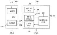
도 10을 참조하면, ECC 회로(400)는 ECC 인코더(410) 및 ECC 디코더(430)를 포함할 수 있다. 입출력 게이팅 회로(290)는 스위칭부(291),기입 드라이버(293) 및 래치부(295)를 포함할 수 있다. 입출력 게이팅 회로(290)는 마스킹 로직(296)을 더 포함할 수 있다. 스위칭부(291)는 도 7 및 도 8의 스위치들(291a~291d)을 포함할 수 있다. 입출력 게이팅 회로(290)는 스크러빙 모드에서 메모리 셀 어레이(300)의 어느 하나의 페이지의 서브 페이지로부터의 독출 코드워드(RCW)를 ECC 디코더(430)에 제공할 수 있다. ECC 디코더(430)는 독출 코드워드(RCW)의 패리티 데이터를 이용하여 독출 코드워드(RCW)의 에러를 정정하여 정정된 코드워드(C_CW)를 입출력 게이팅 회로(290)에 제공할 수 있다. 입출력 게이팅 회로(290)는 ECC 디코더(430)로부터 정정된 코드워드(C_CW)를 제공받아, 에러가 정정된 서브 코드워드만을 상기 서브 페이지에 재기입할 수 있다.Referring to FIG. 10, the
ECC 디코더(430)는 스크러빙 모드에서 제2 제어 신호(CTL2)에 응답하여 상술한 스크러빙 동작을 수행할 수 있다.The
도 11은 독출 동작과 기입 동작시의 3의 반도체 메모리 장치에서 에러 정정 회로와 입출력 게이팅 회로를 나타낸다.11 shows an error correction circuit and an input / output gating circuit in the semiconductor memory device of the third example in the read operation and the write operation.
도 11을 참조하면, 독출 동작에서, 입출력 게이팅 회로(290)는 메모리 셀 어레이(300)의 타겟 페이지로부터의 독출 코드워드(RCW)를 ECC 디코더(430)에 제공하고, ECC 디코더(430)는 독출 코드워드(RCW)의 패리티 데이터를 이용하여 독출 코드워드(RCW)에 포함되는 에러를 정정하여 정정된 메인 데이터(C_MD)를 데이터 입출력 버퍼(299)에 제공할 수 있다.11, in a read operation, the input /
기입 동작에서, 입출력 게이팅 회로(290)는 메모리 셀 어레이(300)의 타겟 페이지의 서브 페이지로부터 독출 코드워드(RCW)를 ECC 디코더(430)에 제공하고, ECC 디코더(430)는 독출 코드워드(RCW)의 에러를 정정하여 정정된 코드워드를 ECC 인코더(410)에 제공할 수 있다. ECC 인코더(410)는 기입 메인 데이터(MD)와 정정된 코드워드에 기초하여 기입 패리티 데이터를 생성하고, 기입 메인 데이터(MD), 정정된 서브 유닛의 데이터 및 기입 패리티 데이터 또는 기입 메인 데이터(MD), 에러를 포함하지 않는 서브 유닛의 데이터 및 기입 패리티 데이터를 포함하는 수정된 코드워드(MCW)를 입출력 게이팅 회로(290)에 제공할 수 있다. 기입 드라이버(293)는 수정된 코드워드(MCW)를 타겟 페이지의 서브 페이지에 기입할 수 있다.
마스킹 로직(296)은 마스크된 기입 동작 시에 메모리 컨트롤러(100)로부터 인가되는 마스크 신호(DM)에 응답하여 기입 드라이버(293)와 ECC 인코더(410)가 마스크된 기입 동작을 수행하도록 할 수 있다.The masking
도 12는 도 7의 반도체 메모리 장치에서 스크러빙 동작이 수행되는 것을 나타낸다.12 shows that the scrubbing operation is performed in the semiconductor memory device of Fig.
도 7, 도 9, 도 10 및 도 12를 참조하면, 커맨드(CMD)가 스크러빙 커맨드인 경우에, 뱅크 어레이(310)의 하나의 페이지의 서브 페이지로부터 64 비트의 제1 서브 유닛(511), 64 비트의 제2 서브 유닛(513) 및 8 비트의 패리티 데이터(PRT)를 포함하는 제1 유닛의 코드워드(CW)가 독출되어(521), ECC 디코더(430)로 제공된다. 제2 서브 유닛(513)은 하나의 에러 비트(ER)를 포함할 수 있다. ECC 디코더(430)는 독출된 제1 유닛의 코드워드(CW)에 대하여 ECC 디코딩(522)를 수행하여 제2 서브 유닛(513)의 에러 비트(ER)를 정정하여 정정된 제2 서브 유닛(513')을 입출력 게이팅 회로(290)에 제공하고, 입출력 게이팅 회로(290)는 정정된 제2 서브 유닛(513')의 데이터를 서브 페이지의 해당 위치에 재기입(write back)한다.Referring to FIGS. 7, 9, 10 and 12, when the command CMD is a scrubbing command, a 64-bit
도 13은 도 8의 반도체 메모리 장치에서 기입 동작이 수행되는 것을 나타낸다.13 shows that a write operation is performed in the semiconductor memory device of Fig.
도 8, 도 9, 도 11 및 도 13을 참조하면, 커맨드(CMD)가 기입 커맨드인 경우에, 뱅크 어레이(310)의 타겟 페이지의 서브 페이지로부터 64 비트의 제1 서브 유닛(511), 64 비트의 제2 서브 유닛(513) 및 8 비트의 패리티 데이터(PRT)를 포함하는 제1 유닛의 코드워드(CW)가 독출되어(531), ECC 디코더(430)로 제공된다. 제2 서브 유닛(513)은 하나의 에러 비트(ER)를 포함할 수 있다. ECC 디코더(430)는 독출된 제1 유닛의 코드워드(CW)에 대하여 ECC 디코딩(522)를 수행하여 제2 서브 유닛(513)의 에러 비트(ER)를 정정하여(532) 정정된 제2 서브 유닛(513')을 ECC 인코더(410)에 제공한다. ECC 인코더(410)는 기입 데이터(MD)와 정정된 제2 서브 유닛(513')에 기초하여 ECC 인코딩을 수행하여 기입 패리티 데이터(PRT')를 생성하고(533) 기입 데이터(MD)와 정정된 제2 서브 유닛(513')과 기입 패리티 데이터(PRT')를 입출력 게이팅 회로(290)에 제공한다. 입출력 게이팅 회로(290)는 기입 데이터(MD)와 정정된 제2 서브 유닛(513')과 기입 패리티 데이터(PRT')를 타겟 페이지의 서브 페이지에 기입한다.8, 9, 11, and 13, when the command CMD is a write command, 64 bits of the
도 14는 도 8의 반도체 메모리 장치에서 기입 동작이 수행되는 것을 나타낸다.14 shows that a write operation is performed in the semiconductor memory device of Fig.
도 8, 도 9, 도 11 및 도 14를 참조하면, 커맨드(CMD)가 기입 커맨드인 경우에, 뱅크 어레이(310)의 타겟 페이지의 서브 페이지로부터 64 비트의 제1 서브 유닛(511), 64 비트의 제2 서브 유닛(513) 및 8 비트의 패리티 데이터(PRT)를 포함하는 제1 유닛의 코드워드(CW)가 독출되어(541), ECC 디코더(430)로 제공된다. 제1 서브 유닛(511)은 하나의 에러 비트(ER)를 포함할 수 있다. ECC 디코더(430)는 독출된 제1 유닛의 코드워드(CW)에 대하여 ECC 디코딩(522)을 수행하여 제1 서브 유닛(511)의 에러 비트(ER)를 정정하여(532) 정정된 제1 서브 유닛(511')을 ECC 인코더(410)에 제공한다. ECC 인코더(410)는 기입 데이터(MD)와 제2 서브 유닛(513)에 기초하여 ECC 인코딩을 수행하여 기입 패리티 데이터(PRT')를 생성하고(533) 기입 데이터(MD)와 기입 패리티 데이터(PRT')를 입출력 게이팅 회로(290)에 제공한다. 입출력 게이팅 회로(290)는 기입 데이터(MD)와 기입 패리티 데이터(PRT')를 타겟 페이지의 서브 페이지에 기입한다.8, 9, 11, and 14, when the command CMD is a write command, 64 bits of the
도 15는 도 10의 에러 정정 회로에서 ECC 인코더를 나타낸다.15 shows an ECC encoder in the error correction circuit of Fig.
도 15를 참조하면, ECC 인코더(410)는 패리티 생성기(411)를 포함할 수 있다. 패리티 생성기(411)는 기입 동작에서 기입 데이터(MD)에 대하여 ECC 인코딩을 수행하여 패리티 데이터(PRT)를 생성하고, 기입 데이터(MD)와 패리티 데이터(PRT)를 포함하는 코드워드(CW)를 입출력 게이팅 회로(290)에 제공할 수 있다.Referring to FIG. 15, the
도 16은 도 10의 에러 정정 회로에서 ECC 디코더를 나타낸다.16 shows an ECC decoder in the error correction circuit of Fig.
도 16을 참조하면, ECC 디코더(430)는 체크 비트 생성기(431), 신드롬 생성기(433) 및 데이터 정정기(435)를 포함할 수 있다.Referring to FIG. 16, the
체크 비트 생성기(431)는 독출 데이터(RMD)를 기초로 하여 체크 비트들(CHB)을 생성할 수 있다. 신드롬 생성기(433)는 체크 비트들(CHB)과 독출 코드워드에 포함되는 패리티 데이터(PRT)를 기초로 독출 데이터(RMD)에 에러가 존재하는지 여부와 에러의 위치를 나타내는 신드롬 데이터(SDR)를 생성할 수 있다. 데이터 정정기(435)는 신드롬 데이터(SDR)에 기초하여 독출 데이터(RMD)의 에러를 정정하고, 스크러빙 모드에서는 정정된 코드워드(C_CW)를 입출력 게이팅 회로(290)에 제공하고, 독출 동작에서는 정정된 메인 데이터(C_MD)를 데이터 입출력 버퍼(299)에 제공할 수 있다.The
도 17은 본 발명의 실시예들에 따른 반도체 메모리 장치의 동작 방법을 나타내는 흐름도이다.17 is a flowchart showing a method of operating a semiconductor memory device according to embodiments of the present invention.
도 2, 도 3, 도 7, 도 9, 도 10, 도 12, 도 15 내지 도 17을 참조하면, 메모리 셀 어레이(300)와 에러 정정 회로(400)를 포함하는 반도체 메모리 장치(200a)의 동작 방법에서는 메모리 컨트롤러(100)로부터 제1 커맨드를 수신한다(S610).Referring to FIGS. 2, 3, 7, 9, 10, 12 and 15 to 17, a
커맨드 디코더(211)는 상기 제1 커맨드를 디코딩하고, 상기 제1 커맨드가 스크러빙 커맨드인 경우에, 상기 제1 커맨드에 응답하여 메모리 셀 어레이(300)의 하나의 뱅크 어레이(310)의 하나의 페이지의 적어도 하나의 서브 페이지를 선택하고, 상기 서브 페이지로부터 적어도 두 개의 서브 유닛들(511, 513) 및 패리티 데이터(PRT)를 구비하는 제1 유닛(CW)의 데이터를 독출한다(S620).The
에러 정정 회로(400)의 ECC 디코더(430)에서 신드롬 데이터(SDR)를 생성하여(S630)하여 제1 유닛(CW)의 데이터에 에러가 존재하는지 여부를 판단한다(S640). 즉 신드롬 생성기(433)는 체크 비트들(CHB)과 패리티 데이터(PRT)의 동일성 여부를 판단하여 신드롬 데이터(SDR)를 생성한다. 신드롬 데이터(SDR)의 적어도 하나의 비트가 '0'이 아닌 경우에는 제1 유닛(CW)의 데이터에 에러가 존재하는 것이다.The
제1 유닛(CW)의 데이터에 에러가 존재하는 경우(S640에서 YES), 신드롬 데이터(SDR)를 기초하여 에러의 위치를 판단하고(S650), 상기 제1 유닛의 데이터(CW) 중 패리티 데이터(PRT)를 이용하여 상기 에러를 포함하는 서브 유닛(513)의 데이터를 정정한다(S660). 입출력 게이팅 회로(290)는 정정된 서브 유닛(513') 데이터만을 뱅크 어레이(310)의 서브 페이지의 해당 위치에 재기입한다(S670).If there is an error in the data of the first unit CW (YES in S640), the position of the error is determined based on the syndrome data SDR (S650), and parity data (PRT) to correct the data of the
스크러빙 동작이 완료된 후나, 제1 유닛(CW)의 데이터에 에러가 존재하지 않는 경우(S640에서 NO), 반도체 메모리 장치(200a)는 메모리 컨트롤러(100)로부터 제2 커맨드를 수신할 수 있다.The
여기서 스크러빙 커맨드는 상술한 바와 같이, 신규하게 정의될 수도 있고, 기 정의된 커맨드들 중 하나를 이용할 수 있다. 구체적으로는, 메모리 셀 어레이(300)에 대한 독출 동작을 위한 독출 커맨드와 서로 다른 신호의 조합(예컨대, /CS, /RAS, /CAS 및 /WE 등의 신호의 조합)을 갖는 커맨드(예컨대, 스크러빙 커맨드)가 신규하게 정의되고, 상기 커맨드에 응답하여 스크러빙 동작이 수행될 수 있다. 즉, 스크러빙 커맨드를 정의하는 경우, 메모리 컨트롤러(100)와 반도체 메모리 장치(200a) 사이의 협의에 의하여 /CS, /RAS, /CAS 및 /WE 등의 신호의 논리 하이 또는 논리 로우를 설정하여 상기 스크러빙 커맨드를 정의할 수 있다.Here, the scrubbing command may be newly defined as described above, or one of the predefined commands may be used. Concretely, a command having a combination of a read command for a read operation with respect to the
또는, 메모리 동작을 위한 다수의 커맨드들 중, 리프레쉬 커맨드에 응답하여 스크러빙 동작이 수행될 수 있다. 스크러빙 커맨드에 응답하여 제1 뱅크 어레이(310)의 어느 하나의 페이지(예를 들어 제1 페이지)가 활성화된다. 상기 활성화된 페이지 내의 하나 이상의 서브 페이지를 순차적으로 선택한다. 선택된 서브 페이지에 대해 스크러빙 동작(에러 검출/정정 및 라이트 백 동작)을 수행할 수 있다. 이와 같은 동작이 완료되면 활성화된 페이지를 비활성화시키며, 이후 스크러빙 커맨드가 수신되면 다음의 하나의 페이지(예컨대, 제2 페이지)가 활성화될 수 있다.Alternatively, a scrubbing operation may be performed in response to a refresh command, among a plurality of commands for a memory operation. In response to the scrubbing command, one of the pages (e.g., the first page) of the
신규하게 정의되는 스크러빙 커맨드를 이용하는 경우, 하나의 스크러빙 커맨드에 응답하여 하나의 페이지에 포함되는 모든 서브 페이지들에 대한 스크러빙 동작을 수행할 수 있다. 반면에, 오토 리프레쉬 커맨드를 이용하는 경우, 하나의 스크러빙 커맨드에 응답하여 하나의 서브 페이지에 대한 스크러빙 동작을 수행할 수 있다.When a newly defined scrubbing command is used, a scrubbing operation can be performed on all subpages included in one page in response to one scrubbing command. On the other hand, when the auto refresh command is used, a scrubbing operation for one sub page can be performed in response to one scrubbing command.
도 18은 본 발명의 실시예들에 따른 반도체 메모리 장치의 동작 방법을 나타내는 흐름도이다.18 is a flowchart showing an operation method of the semiconductor memory device according to the embodiments of the present invention.
도 2, 도 3, 도 8, 도 9, 도 11, 도 13 내지 도 16 및 도 18을 참조하면, 메모리 셀 어레이(300)와 에러 정정 회로(400)를 포함하는 반도체 메모리 장치(200a)의 동작 방법에서는 메모리 컨트롤러(100)로부터 제1 커맨드를 수신한다(S705).Referring to FIGS. 2, 3, 8, 9, 11, 13 to 16, and 18, a
커맨드 디코더(211)는 상기 제1 커맨드를 디코딩하고, 상기 제1 커맨드가 기입 커맨드인 경우에, 상기 제1 커맨드에 응답하여 메모리 셀 어레이(300)의 하나의 뱅크 어레이(310)의 하나의 페이지의 적어도 하나의 서브 페이지를 선택하고, 상기 서브 페이지로부터 적어도 두 개의 서브 유닛들(511, 513) 및 패리티 데이터(PRT)를 구비하는 제1 유닛(CW)의 데이터를 독출한다(S710).The
에러 정정 회로(400)의 ECC 디코더(430)에서 신드롬 데이터(SDR)를 생성하여(S720)하여 제1 유닛(CW)의 데이터에 에러가 존재하는지 여부를 판단한다(S730). 제1 유닛(CW)의 데이터에 에러가 존재하는 경우(S730에서 YES), 신드롬 데이터(SDR)에 기초하여 에러의 위치를 판단하고(S740), 상기 제1 유닛의 데이터(CW) 중 패리티 데이터(PRT)를 이용하여 상기 에러를 포함하는 서브 유닛(511)의 데이터를 정정한다(S750). 에러가 정정된 제1 유닛의 데이터를 ECC 인코더(410)에 제공한다(S760).The
ECC 인코더(410)는 에러가 정정된 제1 유닛의 데이터와 기입 데이터(MD)에 기초하여 코드워드를 정정하고(S760), 정정된 코드워드에 기초하여 새로운 기입 패리티 데이터를 생성한다(S770). ECC 인코더(410)는 수정된 코드워드와 기입 패리티 데이터를 입출력 게이팅 회로(290)에 제공하고, 입출력 게이팅 회로(290)는 기입 데이터 및 기입 패리티 데이터를 적어도 포함하는 수정된 코드워드를 뱅크 어레이의 타겟 페이지의 서브 페이지에 기입한다(S780). 즉 입출력 게이팅 회로(290)는 기입 데이터, 정정된 서브 유닛의 데이터와 기입 패리티 데이터나 기입 데이터 및 기입 패리티 데이터를 뱅크 어레이의 타겟 페이지의 서브 페이지에 기입할 수 있다.The
기입 동작이 완료된 후나, 제1 유닛(CW)의 데이터에 에러가 존재하지 않는 경우(S730에서 NO), 반도체 메모리 장치(200a)는 메모리 컨트롤러(100)로부터 제2 커맨드를 수신할 수 있다.The
도 17 및 도 18에서, 상기 제1 유닛은 반도체 메모리 장치(200a)의 코드워드 단위에 해당하고, 상기 서브 유닛은 상기 반도체 메모리 장치(200a)의 프리페치(pre-fetch) 단위에 해당할 수 있다.17 and 18, the first unit corresponds to a code word unit of the
도 19는 본 발명의 실시예들에 따른 반도체 메모리 장치를 나타내는 구조도이다.19 is a structural diagram showing a semiconductor memory device according to embodiments of the present invention.
도 19에 도시된 바와 같이, 반도체 메모리 장치(600)는 다수의 반도체 레이어들(LA1 내지 LAk, k는 3이상의 자연수)을 구비할 수 있으며, 가장 아래에 위치하는 반도체 레이어(LA1)는 마스터 칩인 것으로 가정하며 또한 나머지 반도체 레이어들(LA2 내지 LAk)은 슬레이브 칩인 것으로 가정한다. 다수의 반도체 레이어들(LA1 내지 LAk)은 관통 실리콘 비아(TSV)를 통해 신호를 서로 송수신하며, 마스터 칩(LA1)은 외면에 형성된 도전 수단(미도시)을 통해 외부의 메모리 컨트롤러(미도시)와 통신한다. 마스터 칩으로서 제1 반도체 레이어(610)와 슬레이브 칩으로서 제k 반도체 레이어(620)를 중심으로 하여 반도체 메모리 장치(600)의 구성 및 동작을 설명하면 다음과 같다.19, the
제1 반도체 레이어(610)는 슬레이브 칩들에 구비되는 메모리 영역(Memory region, 621)을 구동하기 위한 각종 주변 회로들을 구비한다. 예컨데, 제1 반도체 레이어(610)는 메모리의 워드라인을 구동하기 위한 로우 드라이버(X-Driver, 6101)와, 메모리의 비트라인을 구동하기 위한 칼럼 드라이버(Y-Driver, 6102)와, 데이터의 입출력을 제어하기 위한 데이터 입출력부(6103), 외부로부터 커맨드(CMD)를 입력받아 버퍼링하는 커맨드 버퍼(6104)와, 외부로부터 어드레스를 입력받아 버퍼링하는 어드레스 버퍼(6105) 등을 구비할 수 있다. 메모리 영역은 도 3, 도 7 및 도 8을 참조하여 설명한 바와 같이 복수의 뱅크 어레이들을 포함할 수 있다.The
또한 제1 반도체 레이어(610)는 제어 로직(6107)을 더 포함할 수 있다. 제어 로직(6107)은 메모리 컨트롤러(미도시)로부터 제공되는 커맨드 및 어드레스 신호에 기초하여 메모리 영역(621)에 대한 액세스를 제어하고, 제어 신호들을 생성할 수 있다.The
한편, 제k 반도체 레이어(620)는, 메모리 영역(621)에 저장될 데이터에 대하여 ECC 인코딩을 수행하고, 메모리 영역(621)으로부터 독출된 데이터에 대하여 ECC 디코딩을 수행하는 에러 정정 회로(622)를 포함할 수 있다. 에러 정정 회로(622)는 스크러빙 모드에서, 메모리 영역(621)의 하나의 페이지를 활성화시키고, 활성화된 페이지의 복수의 서브 페이지들 중 하나를 선택하고, 선택된 서브 페이지로부터, 적어도 두 개의 서브 유닛의 데이터 및 패리티 데이터를 포함하는 제1 유닛의 데이터를 독출하고 상기 패리티 데이터를 이용하여 제1 유닛의 데이터 중 에러를 포함하는 서브 유닛의 데이터를 정정하고, 정정된 서브 유닛의 데이터를 상기 서브 페이지에 재기입(write-back)하는 스크러빙(scrubbing) 동작을 수행할 수 있다. 따라서 반도체 메모리 장치(600)에서는 스크러빙 동작시의 전력 소모를 감소시킬 수 있다.The
도 20은 본 발명의 실시예에 따른 반도체 메모리 장치가 적용된 메모리 시스템 나타내는 블록도이다.20 is a block diagram showing a memory system to which a semiconductor memory device according to an embodiment of the present invention is applied.
도 20을 참조하면, 메모리 시스템(700)은 메모리 모듈(710) 및 메모리 컨트롤러(720)를 포함할 수 있다. 메모리 모듈(710)은 모듈 보드(Module Board) 상에 장착되는 적어도 하나의 반도체 메모리 장치(730)를 포함할 수 있다. 반도체 메모리 장치(730)는 도 3의 반도체 메모리 장치(200a)로 구현될 수 있다. 예컨대, 반도체 메모리 장치(730)는 DRAM 칩이나 MRAM 칩으로 구현될 수 있다. 또한, 각각의 반도체 메모리 장치(730)는 서로 적층된 복수의 반도체 칩들을 포함할 수 있다. 이 경우, 반도체 칩들은 적어도 하나의 마스터 칩(731)과 적어도 하나의 슬레이브 칩(732)을 포함할 수 있다. 서로 적층된 반도체 칩들 사이의 신호의 전달은 관통 실리콘 비아(TSV)를 통하여 수행될 수 있다.Referring to FIG. 20,
마스터 칩(731)과 슬레이브 칩(732)은 도 3의 반도체 메모리 장치(200a)를 포함할 수 있다. 따라서 반도체 메모리 장치는 도 2 내지 도 18을 참조하여 설명한 바와 같이, 에러 정정 회로와 메모리 셀 어레이를 포함할 수 있다. 에러 정정 회로는 스크러빙 모드에서, 메모리 셀 어레이의 하나의 페이지를 활성화시키고, 활성화된 페이지의 복수의 서브 페이지들 중 하나를 선택하고, 선택된 서브 페이지로부터, 적어도 두 개의 서브 유닛의 데이터 및 패리티 데이터를 포함하는 제1 유닛의 데이터를 독출하고 상기 패리티 데이터를 이용하여 제1 유닛의 데이터 중 에러를 포함하는 서브 유닛의 데이터를 정정하고, 정정된 서브 유닛의 데이터를 상기 서브 페이지에 재기입(write-back)하는 스크러빙(scrubbing) 동작을 수행할 수 있다. 따라서 메모리 시스템(700)에서는 스크러빙 동작시의 전력 소모를 감소시킬 수 있다.The
또한 반도체 메모리 장치(730)에는 3차원 메모리 어레이가 제공될 수 있다. 상기 3차원 메모리 어레이는 실리콘 기판 상에 배치된 액티브 이ㅕ역을 구비하는 하나 이상의 물리적 레벨의 메모리 셀 어레이들 및 상기 메모리 셀들의 동작과 관련된 회로들이 모놀리딕(monolithic) 방식으로 형성될 수 있다. 여기서 'monolithic'이라는 용어는 복수의 레이어들로 구성된 어레이의 각 레벨이 하위 레이어 위에 직접적으로 적층되는 것을 의미한다. 본 발명에 참조로서 포함되는 다음의 특허 문헌들은 상기 3차원 메모리 어레이 대한 적절한 구성들을 기술한다. 상기 3차원 메모리 어레이에서 워드라인들 및/또는 비트라인들이 레벨들 사이에서 공유된다. 상기 특허문헌들은 다음과 같다: 미국 등록 특허 7,679,133; 8,553,466; 8,654,587; 8,559,235; 및 미국 공개 특허 2011/0233648.Also, the
메모리 모듈(710)은 시스템 버스를 통해 메모리 컨트롤러(720)와 통신할 수 있다. 시스템 버스를 통하며 메인 데이터(MD), 커맨드/어드레스(CMD/ADDR) 및 클록 신호(CLK) 등이 메모리 모듈(710)과 메모리 컨트롤러(720) 사이에서 송수신될 수 있다.
도 21은 본 발명의 실시예들에 따른 반도체 메모리 장치를 컴퓨팅 시스템에 응용한 예를 나타내는 블록도이다.21 is a block diagram showing an example of application of a semiconductor memory device according to embodiments of the present invention to a computing system.
도 21을 참조하면, 컴퓨팅 시스템(1100)은 프로세서(1110), 입출력 허브(1120), 입출력 컨트롤러 허브(1130), 적어도 하나의 메모리 모듈(1140) 및 그래픽 카드(1150)를 포함한다. 실시예에 따라, 컴퓨팅 시스템(1100)은 개인용 컴퓨터(Personal Computer; PC), 서버 컴퓨터(Server Computer), 워크스테이션(Workstation), 노트북(Laptop), 휴대폰(Mobile Phone), 스마트 폰(Smart Phone), 개인 정보 단말기(personal digital assistant; PDA), 휴대형 멀티미디어 플레이어(portable multimedia player; PMP), 디지털 카메라(Digital Camera), 디지털 TV(Digital Television), 셋-탑 박스(Set-Top Box), 음악 재생기(Music Player), 휴대용 게임 콘솔(portable game console), 네비게이션(Navigation) 시스템 등과 같은 임의의 컴퓨팅 시스템일 수 있다.21, the
프로세서(1110)는 특정 계산들 또는 태스크들과 같은 다양한 컴퓨팅 기능들을 실행할 수 있다. 예를 들어, 프로세서(1110)는 마이크로프로세서 또는 중앙 처리 장치(Central Processing Unit; CPU)일 수 있다. 실시예에 따라, 프로세서(1110)는 하나의 프로세서 코어(Single Core)를 포함하거나, 복수의 프로세서 코어들(Multi-Core)을 포함할 수 있다. 예를 들어, 프로세서(1110)는 듀얼 코어(Dual-Core), 쿼드 코어(Quad-Core), 헥사 코어(Hexa-Core) 등의 멀티 코어(Multi-Core)를 포함할 수 있다. 또한, 도 21에는 하나의 프로세서(1110)를 포함하는 컴퓨팅 시스템(1100)이 도시되어 있으나, 실시예에 따라, 컴퓨팅 시스템(1100)은 복수의 프로세서들을 포함할 수 있다. 또한, 실시예에 따라, 프로세서(1110)는 내부 또는 외부에 위치한 캐시 메모리(Cache Memory)를 더 포함할 수 있다.The
프로세서(1110)는 메모리 모듈(1140)의 동작을 제어하는 메모리 컨트롤러(1111)를 포함할 수 있다. 프로세서(1110)에 포함된 메모리 컨트롤러(1111)는 집적 메모리 컨트롤러(Integrated Memory Controller; IMC)라 불릴 수 있다. 메모리 컨트롤러(1111)와 메모리 모듈(1140) 사이의 메모리 인터페이스는 복수의 신호선들을 포함하는 하나의 채널로 구현되거나, 복수의 채널들로 구현될 수 있다. 또한, 각 채널에는 하나 이상의 메모리 모듈(1140)이 연결될 수 있다. 실시예에 따라, 메모리 컨트롤러(1111)는 입출력 허브(1120) 내에 위치할 수 있다. 메모리 컨트롤러(1111)를 포함하는 입출력 허브(1520)는 메모리 컨트롤러 허브(Memory Controller Hub; MCH)라 불릴 수 있다.The
메모리 모듈(1140)은 메모리 컨트롤러(1111)로부터 제공된 데이터를 저장하는 반도체 메모리 장치들을 포함할 수 있다. 상기 반도체 메모리 장치들 각각은 도 2 내지 도 17을 참조하여 설명한 바와 같이, 에러 정정 회로와 메모리 셀 어레이를 포함하여 전술한 스크러빙 동작과 전술한 기입 동작을 수행하여 전력 소모를 감소시킬 수 있다.
입출력 허브(1120)는 그래픽 카드(1150)와 같은 장치들과 프로세서(1110) 사이의 데이터 전송을 관리할 수 있다. 입출력 허브(1120)는 다양한 방식의 인터페이스를 통하여 프로세서(1510)에 연결될 수 있다. 예를 들어, 입출력 허브(1120)와 프로세서(1110)는, 프론트 사이드 버스(Front Side Bus; FSB), 시스템 버스(System Bus), 하이퍼트랜스포트(HyperTransport), 라이트닝 데이터 트랜스포트(Lightning Data Transport; LDT), 퀵패스 인터커넥트(QuickPath Interconnect; QPI), 공통 시스템 인터페이스(Common System Interface; CSI) 등의 다양한 표준의 인터페이스로 연결될 수 있다. 도 111에는 하나의 입출력 허브(1120)를 포함하는 컴퓨팅 시스템(1100)이 도시되어 있으나, 실시예에 따라, 컴퓨팅 시스템(1100)은 복수의 입출력 허브들을 포함할 수 있다.The I /
입출력 허브(1120)는 장치들과의 다양한 인터페이스들을 제공할 수 있다. 예를 들어, 입출력 허브(1120)는 가속 그래픽 포트(Accelerated Graphics Port; AGP) 인터페이스, 주변 구성요소 인터페이스-익스프레스(Peripheral Component Interface-Express; PCIe), 통신 스트리밍 구조(Communications Streaming Architecture; CSA) 인터페이스 등을 제공할 수 있다.The I /
그래픽 카드(1150)는 AGP 또는 PCIe를 통하여 입출력 허브(1520)와 연결될 수 있다. 그래픽 카드(1150)는 영상을 표시하기 위한 디스플레이 장치(미도시)를 제어할 수 있다. 그래픽 카드(1150)는 이미지 데이터 처리를 위한 내부 프로세서 및 내부 반도체 메모리 장치를 포함할 수 있다. 실시예에 따라, 입출력 허브(1120)는, 입출력 허브(1120)의 외부에 위치한 그래픽 카드(1150)와 함께, 또는 그래픽 카드(1150) 대신에 입출력 허브(1120)의 내부에 그래픽 장치를 포함할 수 있다. 입출력 허브(1520)에 포함된 그래픽 장치는 집적 그래픽(Integrated Graphics)이라 불릴 수 있다. 또한, 메모리 컨트롤러 및 그래픽 장치를 포함하는 입출력 허브(1120)는 그래픽 및 메모리 컨트롤러 허브(Graphics and Memory Controller Hub; GMCH)라 불릴 수 있다.
입출력 컨트롤러 허브(1130)는 다양한 시스템 인터페이스들이 효율적으로 동작하도록 데이터 버퍼링 및 인터페이스 중재를 수행할 수 있다. 입출력 컨트롤러 허브(1130)는 내부 버스를 통하여 입출력 허브(1120)와 연결될 수 있다. 예를 들어, 입출력 허브(1120)와 입출력 컨트롤러 허브(1130)는 다이렉트 미디어 인터페이스(Direct Media Interface; DMI), 허브 인터페이스, 엔터프라이즈 사우스브릿지 인터페이스(Enterprise Southbridge Interface; ESI), PCIe 등을 통하여 연결될 수 있다.The input /
입출력 컨트롤러 허브(1530)는 주변 장치들과의 다양한 인터페이스들을 제공할 수 있다. 예를 들어, 입출력 컨트롤러 허브(1130)는 범용 직렬 버스(Universal Serial Bus; USB) 포트, 직렬 ATA(Serial Advanced Technology Attachment; SATA) 포트, 범용 입출력(General Purpose Input/Output; GPIO), 로우 핀 카운트(Low Pin Count; LPC) 버스, 직렬 주변 인터페이스(Serial Peripheral Interface; SPI), PCI, PCIe 등을 제공할 수 있다.I / O controller hub 1530 may provide various interfaces with peripheral devices. For example, the input /
실시예에 따라, 프로세서(1110), 입출력 허브(1120) 및 입출력 컨트롤러 허브(1130)는 각각 분리된 칩셋들 또는 집적 회로들로 구현되거나, 프로세서(1110), 입출력 허브(1120) 또는 입출력 컨트롤러 허브(1130) 중 2 이상의 구성요소들이 하나의 칩셋으로 구현될 수 있다.The
본 발명은 반도체 메모리 장치를 사용하는 시스템에 적용될 수 있다. 예를 들어, 본 발명은 휴대폰(Mobile Phone), 스마트 폰(Smart Phone), 개인 정보 단말기(personal digital assistant; PDA), 휴대형 멀티미디어 플레이어(portable multimedia player; PMP), 디지털 카메라(Digital Camera), 캠코더(Camcoder), 개인용 컴퓨터(Personal Computer; PC), 서버 컴퓨터(Server Computer), 워크스테이션(Workstation), 노트북(Laptop), 디지털 TV(Digital Television), 셋-탑 박스(Set-Top Box), 음악 재생기(Music Player), 휴대용 게임 콘솔(Portable Game Console), 네비게이션(Navigation) 시스템, 스마트 카드(Smart Card), 프린터(Printer) 등에 유용하게 이용될 수 있다.The present invention can be applied to a system using a semiconductor memory device. For example, the present invention can be applied to a mobile phone, a smart phone, a personal digital assistant (PDA), a portable multimedia player (PMP), a digital camera, a camcorder A computer, a camcoder, a personal computer (PC), a server computer, a workstation, a laptop, a digital television, a set-top box, A music player, a portable game console, a navigation system, a smart card, a printer, and the like.
상술한 바와 같이, 본 발명의 실시예들을 참조하여 설명하였지만, 해당 기술 분야에서 통상의 지식을 가진 자는 하기의 특허청구범위에 기재된 본 발명의 사상 및 영역으로부터 벗어나지 않는 범위 내에서 본 발명을 다양하게 수정 및 변경시킬 수 있음을 이해할 것이다.While the present invention has been described with reference to exemplary embodiments, it is to be understood that the invention is not limited to the disclosed exemplary embodiments, but, on the contrary, is intended to cover various modifications and equivalent arrangements included within the spirit and scope of the appended claims. It will be understood that the invention may be varied and changed without departing from the scope of the invention.
100: 메모리 컨트롤러200a: 반도체 메모리 장치
210: 제어 로직 회로290: 입출력 게이팅 회로
300: 메모리 셀 어레이400: 에러 정정 회로100:
210: control logic circuit 290: input / output gating circuit
300: memory cell array 400: error correction circuit
Claims (20)
Translated fromKorean외부의 메모리 컨트롤러로부터 수신된 제1 커맨드에 응답하여 상기 메모리 셀 어레이의 하나의 페이지의 적어도 하나의 서브 페이지를 선택하는 단계;
상기 서브 페이지로부터 적어도 두 개의 서브 유닛들 및 패리티 데이터를 구비하는 제1 유닛의 데이터를 독출하는 단계;
상기 독출된 제1 유닛의 데이터에 대하여 에러를 존재하는지 여부를 판단하는 단계;
상기 독출된 제1 유닛의 데이터에 에러가 존재하는 경우, 상기 제1 유닛의 데이터 중 상기 패리티 데이터를 이용하여 상기 에러를 포함하는 서브 유닛의 데이터를 정정하는 단계; 및
상기 정정된 서브 유닛을 상기 서브 페이지에 재기입하는 단계를 포함하는 반도체 메모리 장치의 동작 방법.In an operation method of a semiconductor memory device having a memory cell array and an error correction circuit,
Selecting at least one subpage of one page of the memory cell array in response to a first command received from an external memory controller;
Reading data of a first unit having at least two sub-units and parity data from the sub-page;
Determining whether there is an error in the data of the first unit read out;
Correcting data of the sub unit including the error using the parity data among the data of the first unit when an error exists in the data of the read first unit; And
And rewriting the corrected sub-unit in the sub-page.
상기 외부의 메모리 컨트롤러로부터 제2 커맨드를 수신하는 단계를 더 포함하는 반도체 메모리 장치의 동작 방법.The method according to claim 1,
And receiving a second command from the external memory controller.
상기 제1 유닛은 상기 반도체 메모리 장치의 코드워드 단위에 해당하고, 상기 서브 유닛은 상기 반도체 메모리 장치의 프리페치(pre-fetch) 단위에 해당하는 반도체 메모리 장치의 동작 방법.The method according to claim 1,
Wherein the first unit corresponds to a code word unit of the semiconductor memory device, and the sub-unit corresponds to a pre-fetch unit of the semiconductor memory device.
상기 에러 정정 회로에서 상기 독출된 제1 유닛의 데이터에 기초하여 신드롬 데이터를 생성하여 수행되는 반도체 메모리 장치의 동작 방법.2. The method of claim 1, wherein determining whether the error is present comprises:
And generating syndrome data based on the read data of the first unit in the error correction circuit.
상기 제1 커맨드는 상기 반도체 메모리 장치의 독출 동작을 위한 독출 커맨드와 서로 다른 신호 조합으로 구성되는 스크러빙 커맨드인 반도체 메모리 장치의 동작 방법.The method according to claim 1,
Wherein the first command is a scrubbing command composed of a read command for a read operation of the semiconductor memory device and a different signal combination.
상기 메모리 셀 어레이는 복수의 뱅크 어레이들을 포함하고, 상기 뱅크 어레이들 각각은 복수의 페이지들을 구비하고, 각각의 페이지는 복수의 서브 페이지들을 포함하고,
상기 제1 커맨드에 의하여 하나의 페이지가 활성화되고, 활성화된 페이지의 적어도 두 개의 서브 페이지에 대하여 정정된 서브 유닛이 재기입되는 반도체 메모리 장치의 동작 방법.6. The method of claim 5,
The memory array comprising a plurality of bank arrays, each of the bank arrays having a plurality of pages, each page comprising a plurality of sub-pages,
Wherein one page is activated by the first command and the corrected subunit is rewritten for at least two subpages of the activated page.
상기 제1 커맨드는 일정한 주기에 따라 수신되고,
상기 메모리 셀 어레이는 복수의 뱅크 어레이들을 포함하고, 상기 뱅크 어레이들 각각은 복수의 페이지들을 구비하고,
상기 복수의 페이지들은 상기 제1 커맨드가 수신됨에 따라 순차적으로 활성화되고,
상기 활성화된 하나의 페이지의 복수의 서브 페이지들이 순차적으로 선택되는 반도체 메모리 장치의 동작 방법.The method according to claim 1,
Wherein the first command is received in a predetermined period,
The memory cell array including a plurality of bank arrays, each of the bank arrays having a plurality of pages,
Wherein the plurality of pages are sequentially activated as the first command is received,
And a plurality of subpages of the activated one page are sequentially selected.
상기 제1 커맨드는 상기 반도체 메모리 장치의 리프레쉬 동작을 위한 리프레쉬 커맨드인 반도체 메모리 장치의 동작 방법.The method according to claim 1,
Wherein the first command is a refresh command for a refresh operation of the semiconductor memory device.
상기 메모리 셀 어레이는 복수의 뱅크 어레이들을 포함하고, 상기 뱅크 어레이들 각각은 복수의 페이지들을 구비하고,
상기 리프레쉬 커맨드에 응답하여 어느 하나의 페이지가 활성화되고, 활성화된 페이지의 하나의 서브 페이지에 대하여 정정된 서브 유닛이 재기입되는 반도체 메모리 장치.9. The method of claim 8,
The memory cell array including a plurality of bank arrays, each of the bank arrays having a plurality of pages,
One of the pages is activated in response to the refresh command, and the corrected sub-unit is rewritten to one sub-page of the activated page.
외부의 메모리 컨트롤러로부터 수신된 제1 커맨드에 응답하여 상기 메모리 셀 어레이의 하나의 페이지의 적어도 하나의 서브 페이지를 선택하는 단계;
상기 서브 페이지로부터 적어도 두 개의 서브 유닛들 및 패리티 데이터를 구비하는 제1 유닛의 데이터를 독출하는 단계;
상기 독출된 제1 유닛의 데이터에 대하여 에러를 존재하는지 여부를 판단하는 단계;
상기 독출된 제1 유닛의 데이터에 에러가 존재하는 경우, 상기 제1 유닛의 데이터 중 패리티 데이터를 이용하여 상기 에러를 포함하는 서브 유닛의 데이터를 정정하는 단계;
기입 데이터 및 상기 정정된 서브 유닛의 데이터에 기초하여 기입 패리티 데이터를 생성하는 단계; 및
상기 기입 데이터 및 상기 패리티 데이터를 적어도 포함하는 수정된 코드워드를 상기 서브 페이지에 기입하는 단계를 포함하는 반도체 메모리 장치의 동작 방법.In an operation method of a semiconductor memory device having a memory cell array and an error correction circuit,
Selecting at least one subpage of one page of the memory cell array in response to a first command received from an external memory controller;
Reading data of a first unit having at least two sub-units and parity data from the sub-page;
Determining whether there is an error in the data of the first unit read out;
Correcting data of a subunit including the error by using parity data among data of the first unit when an error exists in data of the read first unit;
Generating write parity data based on write data and data of the corrected sub-unit; And
Writing the modified codeword including at least the write data and the parity data to the subpage.
상기 외부의 메모리 컨트롤러로부터 제2 커맨드를 수신하는 단계를 더 포함하는 반도체 메모리 장치의 동작 방법.11. The method of claim 10,
And receiving a second command from the external memory controller.
상기 제1 유닛은 상기 반도체 메모리 장치의 코드워드 단위에 해당하고, 상기 서브 유닛과 상기 기입 데이터의 크기는 상기 반도체 메모리 장치의 프리페치(pre-fetch) 단위에 해당하는 반도체 메모리 장치의 동작 방법.11. The method of claim 10,
Wherein the first unit corresponds to a code word unit of the semiconductor memory device and the size of the sub unit and the write data corresponds to a pre-fetch unit of the semiconductor memory device.
상기 서브 페이지에서 상기 정정된 서브 유닛의 데이터가 기입될 위치와 상기 기입 데이터가 기입될 위치가 다른 경우에,
상기 기입 데이터, 상기 정정된 서브 유닛의 데이터 및 상기 기입 패리티 데이터가 상기 수정된 코드워드로서 상기 서브 페이지에 기입되는 반도체 메모리 장치의 동작 방법.11. The method of claim 10,
When the position at which the data of the corrected sub-unit is to be written in the sub page differs from the position at which the write data is to be written,
The write data, the corrected sub-unit data, and the write parity data are written to the sub page as the modified code word.
상기 서브 페이지에서 상기 정정된 서브 유닛의 데이터가 기입될 위치와 상기 기입 데이터가 기입될 위치가 동일한 경우에,
상기 기입 데이터 및 상기 기입 패리티 데이터가 상기 수정된 코드워드로서 상기 서브 페이지에 기입되는 반도체 메모리 장치의 동작 방법.11. The method of claim 10,
When the position at which the data of the corrected sub-unit is to be written in the sub page is the same as the position at which the write data is to be written,
Wherein the write data and the write parity data are written in the sub page as the modified code word.
상기 에러 정정 회로에서 상기 독출된 제1 유닛의 데이터에 기초하여 신드롬 데이터를 생성하여 수행되는 반도체 메모리 장치의 동작 방법.11. The method of claim 10, wherein determining whether the error is present comprises:
And generating syndrome data based on the read data of the first unit in the error correction circuit.
상기 제1 커맨드는 상기 반도체 메모리 장치의 기입 동작을 위한 기입 커맨드인 반도체 메모리 장치의 동작 방법.11. The method of claim 10,
Wherein the first command is a write command for a write operation of the semiconductor memory device.
상기 메모리 셀 어레이는 복수의 뱅크 어레이들을 포함하고, 상기 뱅크 어레이들 각각은 복수의 페이지들을 구비하고,
상기 제1 커맨드에 의하여 어느 하나의 페이지가 선택되고, 상기 선택된 페이지의 복수의 서브 페이지들이 순차적으로 활성화되는 반도체 메모리 장치의 동작 방법.17. The method of claim 16,
The memory cell array including a plurality of bank arrays, each of the bank arrays having a plurality of pages,
Wherein one of the pages is selected by the first command and a plurality of sub pages of the selected page are sequentially activated.
외부의 메모리 컨트롤러로부터의 커맨드를 디코딩하여 제어 신호들을 생성하는 제어 로직 회로; 및
상기 메모리 셀 어레이로부터의 독출 데이터에 대하여 에러 정정 코드(error correction code; 'ECC') 디코딩을 수행하는 에러 정정 회로를 포함하고,
상기 제어 로직 회로는 상기 메모리 컨트롤러로부터 수신된 제1 커맨드에 응답하여 상기 복수의 페이지들 중 하나의 페이지의 적어도 하나의 서브 페이지를 선택하고, 상기 서브 페이지로부터 적어도 두 개의 서브 유닛들 및 패리티 데이터를 구비하는 제1 유닛의 데이터를 독출하여, 에러를 포함하는 서브 유닛의 데이터가 상기 서브 페이지에 재기입되도록 상기 에러 정정 회로를 제어하는 반도체 메모리 장치.A memory cell array including a plurality of bank arrays each having a plurality of pages;
A control logic circuit for decoding a command from an external memory controller to generate control signals; And
And an error correction circuit for performing error correction code (ECC) decoding on the read data from the memory cell array,
Wherein the control logic circuit is responsive to a first command received from the memory controller to select at least one subpage of one page of the plurality of pages and to receive at least two subunits and parity data from the subpage Reads out the data of the first unit and controls the error correction circuit so that the data of the sub unit including the error is rewritten in the sub page.
상기 제1 유닛은 상기 반도체 메모리 장치의 코드워드 단위에 해당하고, 상기 서브 유닛은 상기 반도체 메모리 장치의 프리페치(pre-fetch) 단위에 해당하는 반도체 메모리 장치19. The method of claim 18,
Wherein the first unit corresponds to a code word unit of the semiconductor memory device, and the sub-unit corresponds to a semiconductor memory device corresponding to a pre-fetch unit of the semiconductor memory device,
상기 메모리 셀 어레이는 3차원 메모리 셀 어레이이고,
상기 뱅크 어레이들 각각은 복수의 동적 메모리 셀들 또는 복수의 저항성 메모리 셀들을 포함하는 반도체 메모리 장치.19. The method of claim 18,
The memory cell array is a three-dimensional memory cell array,
Each of the bank arrays comprising a plurality of dynamic memory cells or a plurality of resistive memory cells.
Priority Applications (4)
| Application Number | Priority Date | Filing Date | Title |
|---|---|---|---|
| KR1020150145731AKR20170045806A (en) | 2015-10-20 | 2015-10-20 | Semiconductor memory device and method of operating the same |
| US15/290,339US9990163B2 (en) | 2015-10-20 | 2016-10-11 | Methods of operating semiconductor memory devices with selective write-back of data for error scrubbing and related devices |
| CN201610916491.3ACN106997783B (en) | 2015-10-20 | 2016-10-20 | Semiconductor memory device and method of operating semiconductor memory device |
| US15/969,042US10198221B2 (en) | 2015-10-20 | 2018-05-02 | Methods of operating semiconductor memory devices with selective write-back of data for error scrubbing and related devices |
Applications Claiming Priority (1)
| Application Number | Priority Date | Filing Date | Title |
|---|---|---|---|
| KR1020150145731AKR20170045806A (en) | 2015-10-20 | 2015-10-20 | Semiconductor memory device and method of operating the same |
Publications (1)
| Publication Number | Publication Date |
|---|---|
| KR20170045806Atrue KR20170045806A (en) | 2017-04-28 |
Family
ID=58523902
Family Applications (1)
| Application Number | Title | Priority Date | Filing Date |
|---|---|---|---|
| KR1020150145731AWithdrawnKR20170045806A (en) | 2015-10-20 | 2015-10-20 | Semiconductor memory device and method of operating the same |
Country Status (3)
| Country | Link |
|---|---|
| US (2) | US9990163B2 (en) |
| KR (1) | KR20170045806A (en) |
| CN (1) | CN106997783B (en) |
Cited By (6)
| Publication number | Priority date | Publication date | Assignee | Title |
|---|---|---|---|---|
| KR20190060258A (en)* | 2017-11-24 | 2019-06-03 | 에스케이하이닉스 주식회사 | Error scrub method and semiconductor module using the same |
| KR20190137281A (en)* | 2018-06-01 | 2019-12-11 | 삼성전자주식회사 | Semiconductor memory devices, memory systems including the same and method of operating semiconductor memory devices |
| KR20200032765A (en)* | 2017-08-23 | 2020-03-26 | 마이크론 테크놀로지, 인크 | Memory with virtual page size |
| KR20210006664A (en)* | 2019-07-09 | 2021-01-19 | 에스케이하이닉스 주식회사 | Memory system and operation method thereof |
| US11747982B2 (en) | 2017-08-23 | 2023-09-05 | Micron Technology, Inc. | On-demand memory page size |
| CN118380038A (en)* | 2024-06-21 | 2024-07-23 | 晶铁半导体技术(广东)有限公司 | Ferroelectric memory error correction method, system, equipment and product |
Families Citing this family (84)
| Publication number | Priority date | Publication date | Assignee | Title |
|---|---|---|---|---|
| US10049006B2 (en) | 2015-12-08 | 2018-08-14 | Nvidia Corporation | Controller-based memory scrub for DRAMs with internal error-correcting code (ECC) bits contemporaneously during auto refresh or by using masked write commands |
| US9880900B2 (en)* | 2015-12-08 | 2018-01-30 | Nvidia Corporation | Method for scrubbing and correcting DRAM memory data with internal error-correcting code (ECC) bits contemporaneously during self-refresh state |
| US10198204B2 (en)* | 2016-06-01 | 2019-02-05 | Advanced Micro Devices, Inc. | Self refresh state machine MOP array |
| JP2018160166A (en)* | 2017-03-23 | 2018-10-11 | 東芝メモリ株式会社 | Memory system, and resistance change type memory |
| US10141042B1 (en) | 2017-05-23 | 2018-11-27 | Micron Technology, Inc. | Method and apparatus for precharge and refresh control |
| US10884926B2 (en) | 2017-06-16 | 2021-01-05 | Alibaba Group Holding Limited | Method and system for distributed storage using client-side global persistent cache |
| US10678443B2 (en) | 2017-07-06 | 2020-06-09 | Alibaba Group Holding Limited | Method and system for high-density converged storage via memory bus |
| US10496829B2 (en) | 2017-09-15 | 2019-12-03 | Alibaba Group Holding Limited | Method and system for data destruction in a phase change memory-based storage device |
| US10642522B2 (en) | 2017-09-15 | 2020-05-05 | Alibaba Group Holding Limited | Method and system for in-line deduplication in a storage drive based on a non-collision hash |
| KR20190031787A (en) | 2017-09-18 | 2019-03-27 | 삼성전자주식회사 | Memory device with read-modify-write operation in parallel |
| US10789011B2 (en) | 2017-09-27 | 2020-09-29 | Alibaba Group Holding Limited | Performance enhancement of a storage device using an integrated controller-buffer |
| US10860334B2 (en) | 2017-10-25 | 2020-12-08 | Alibaba Group Holding Limited | System and method for centralized boot storage in an access switch shared by multiple servers |
| US10445190B2 (en)* | 2017-11-08 | 2019-10-15 | Alibaba Group Holding Limited | Method and system for enhancing backup efficiency by bypassing encoding and decoding |
| KR20190054533A (en) | 2017-11-14 | 2019-05-22 | 삼성전자주식회사 | Semiconductor memory devices, memory systems including the same and methods of operating semiconductor memory devices |
| US10877898B2 (en) | 2017-11-16 | 2020-12-29 | Alibaba Group Holding Limited | Method and system for enhancing flash translation layer mapping flexibility for performance and lifespan improvements |
| KR102410566B1 (en)* | 2018-02-05 | 2022-06-17 | 삼성전자주식회사 | Semiconductor memory devices, memory systems including the same and method of operating semiconductor memory devices |
| US10891239B2 (en) | 2018-02-07 | 2021-01-12 | Alibaba Group Holding Limited | Method and system for operating NAND flash physical space to extend memory capacity |
| US10496548B2 (en) | 2018-02-07 | 2019-12-03 | Alibaba Group Holding Limited | Method and system for user-space storage I/O stack with user-space flash translation layer |
| US10831404B2 (en) | 2018-02-08 | 2020-11-10 | Alibaba Group Holding Limited | Method and system for facilitating high-capacity shared memory using DIMM from retired servers |
| JP2019158541A (en)* | 2018-03-12 | 2019-09-19 | 株式会社ミツトヨ | X-ray ct apparatus for measurement and method for measuring mass-produced workpieces |
| KR102580944B1 (en)* | 2018-04-20 | 2023-09-20 | 삼성전자주식회사 | Memory device having an error correction fucntion and operating method thereof |
| US11379155B2 (en) | 2018-05-24 | 2022-07-05 | Alibaba Group Holding Limited | System and method for flash storage management using multiple open page stripes |
| US11010245B2 (en)* | 2018-06-21 | 2021-05-18 | Winbond Electronics Corp. | Memory storage apparatus with dynamic data repair mechanism and method of dynamic data repair thereof |
| CN111902804B (en) | 2018-06-25 | 2024-03-01 | 阿里巴巴集团控股有限公司 | System and method for managing resources of a storage device and quantifying I/O request costs |
| US10921992B2 (en) | 2018-06-25 | 2021-02-16 | Alibaba Group Holding Limited | Method and system for data placement in a hard disk drive based on access frequency for improved IOPS and utilization efficiency |
| US10418125B1 (en)* | 2018-07-19 | 2019-09-17 | Marvell Semiconductor | Write and read common leveling for 4-bit wide DRAMs |
| US10871921B2 (en) | 2018-07-30 | 2020-12-22 | Alibaba Group Holding Limited | Method and system for facilitating atomicity assurance on metadata and data bundled storage |
| US10996886B2 (en) | 2018-08-02 | 2021-05-04 | Alibaba Group Holding Limited | Method and system for facilitating atomicity and latency assurance on variable sized I/O |
| US10747673B2 (en) | 2018-08-02 | 2020-08-18 | Alibaba Group Holding Limited | System and method for facilitating cluster-level cache and memory space |
| US11327929B2 (en) | 2018-09-17 | 2022-05-10 | Alibaba Group Holding Limited | Method and system for reduced data movement compression using in-storage computing and a customized file system |
| US10852948B2 (en) | 2018-10-19 | 2020-12-01 | Alibaba Group Holding | System and method for data organization in shingled magnetic recording drive |
| US10795586B2 (en) | 2018-11-19 | 2020-10-06 | Alibaba Group Holding Limited | System and method for optimization of global data placement to mitigate wear-out of write cache and NAND flash |
| US10769018B2 (en) | 2018-12-04 | 2020-09-08 | Alibaba Group Holding Limited | System and method for handling uncorrectable data errors in high-capacity storage |
| US10795767B2 (en) | 2018-12-26 | 2020-10-06 | M31 Technology Corporation | Error correcting system shared by multiple memory devices |
| US10977122B2 (en) | 2018-12-31 | 2021-04-13 | Alibaba Group Holding Limited | System and method for facilitating differentiated error correction in high-density flash devices |
| US10884654B2 (en) | 2018-12-31 | 2021-01-05 | Alibaba Group Holding Limited | System and method for quality of service assurance of multi-stream scenarios in a hard disk drive |
| US11061735B2 (en) | 2019-01-02 | 2021-07-13 | Alibaba Group Holding Limited | System and method for offloading computation to storage nodes in distributed system |
| US11132291B2 (en) | 2019-01-04 | 2021-09-28 | Alibaba Group Holding Limited | System and method of FPGA-executed flash translation layer in multiple solid state drives |
| JP7219397B2 (en)* | 2019-01-18 | 2023-02-08 | 富士通株式会社 | Information processing device, storage control device and storage control program |
| US10860420B2 (en) | 2019-02-05 | 2020-12-08 | Alibaba Group Holding Limited | Method and system for mitigating read disturb impact on persistent memory |
| US11200337B2 (en) | 2019-02-11 | 2021-12-14 | Alibaba Group Holding Limited | System and method for user data isolation |
| US10970212B2 (en) | 2019-02-15 | 2021-04-06 | Alibaba Group Holding Limited | Method and system for facilitating a distributed storage system with a total cost of ownership reduction for multiple available zones |
| US11061834B2 (en) | 2019-02-26 | 2021-07-13 | Alibaba Group Holding Limited | Method and system for facilitating an improved storage system by decoupling the controller from the storage medium |
| US10783035B1 (en) | 2019-02-28 | 2020-09-22 | Alibaba Group Holding Limited | Method and system for improving throughput and reliability of storage media with high raw-error-rate |
| US10891065B2 (en) | 2019-04-01 | 2021-01-12 | Alibaba Group Holding Limited | Method and system for online conversion of bad blocks for improvement of performance and longevity in a solid state drive |
| US10922234B2 (en) | 2019-04-11 | 2021-02-16 | Alibaba Group Holding Limited | Method and system for online recovery of logical-to-physical mapping table affected by noise sources in a solid state drive |
| US10908960B2 (en) | 2019-04-16 | 2021-02-02 | Alibaba Group Holding Limited | Resource allocation based on comprehensive I/O monitoring in a distributed storage system |
| US11169873B2 (en) | 2019-05-21 | 2021-11-09 | Alibaba Group Holding Limited | Method and system for extending lifespan and enhancing throughput in a high-density solid state drive |
| US10860223B1 (en) | 2019-07-18 | 2020-12-08 | Alibaba Group Holding Limited | Method and system for enhancing a distributed storage system by decoupling computation and network tasks |
| US11126561B2 (en) | 2019-10-01 | 2021-09-21 | Alibaba Group Holding Limited | Method and system for organizing NAND blocks and placing data to facilitate high-throughput for random writes in a solid state drive |
| US11042307B1 (en) | 2020-01-13 | 2021-06-22 | Alibaba Group Holding Limited | System and method for facilitating improved utilization of NAND flash based on page-wise operation |
| US11449455B2 (en) | 2020-01-15 | 2022-09-20 | Alibaba Group Holding Limited | Method and system for facilitating a high-capacity object storage system with configuration agility and mixed deployment flexibility |
| US10872622B1 (en) | 2020-02-19 | 2020-12-22 | Alibaba Group Holding Limited | Method and system for deploying mixed storage products on a uniform storage infrastructure |
| US10923156B1 (en) | 2020-02-19 | 2021-02-16 | Alibaba Group Holding Limited | Method and system for facilitating low-cost high-throughput storage for accessing large-size I/O blocks in a hard disk drive |
| US11150986B2 (en) | 2020-02-26 | 2021-10-19 | Alibaba Group Holding Limited | Efficient compaction on log-structured distributed file system using erasure coding for resource consumption reduction |
| US11144250B2 (en) | 2020-03-13 | 2021-10-12 | Alibaba Group Holding Limited | Method and system for facilitating a persistent memory-centric system |
| US11200114B2 (en) | 2020-03-17 | 2021-12-14 | Alibaba Group Holding Limited | System and method for facilitating elastic error correction code in memory |
| US11385833B2 (en) | 2020-04-20 | 2022-07-12 | Alibaba Group Holding Limited | Method and system for facilitating a light-weight garbage collection with a reduced utilization of resources |
| US11281575B2 (en) | 2020-05-11 | 2022-03-22 | Alibaba Group Holding Limited | Method and system for facilitating data placement and control of physical addresses with multi-queue I/O blocks |
| US11461262B2 (en) | 2020-05-13 | 2022-10-04 | Alibaba Group Holding Limited | Method and system for facilitating a converged computation and storage node in a distributed storage system |
| US11494115B2 (en) | 2020-05-13 | 2022-11-08 | Alibaba Group Holding Limited | System method for facilitating memory media as file storage device based on real-time hashing by performing integrity check with a cyclical redundancy check (CRC) |
| US11218165B2 (en) | 2020-05-15 | 2022-01-04 | Alibaba Group Holding Limited | Memory-mapped two-dimensional error correction code for multi-bit error tolerance in DRAM |
| US11556277B2 (en) | 2020-05-19 | 2023-01-17 | Alibaba Group Holding Limited | System and method for facilitating improved performance in ordering key-value storage with input/output stack simplification |
| US11507499B2 (en) | 2020-05-19 | 2022-11-22 | Alibaba Group Holding Limited | System and method for facilitating mitigation of read/write amplification in data compression |
| US11263132B2 (en) | 2020-06-11 | 2022-03-01 | Alibaba Group Holding Limited | Method and system for facilitating log-structure data organization |
| US11422931B2 (en) | 2020-06-17 | 2022-08-23 | Alibaba Group Holding Limited | Method and system for facilitating a physically isolated storage unit for multi-tenancy virtualization |
| US11354200B2 (en) | 2020-06-17 | 2022-06-07 | Alibaba Group Holding Limited | Method and system for facilitating data recovery and version rollback in a storage device |
| US20210397380A1 (en)* | 2020-06-23 | 2021-12-23 | Micron Technology, Inc. | Dynamic page activation |
| US11354233B2 (en) | 2020-07-27 | 2022-06-07 | Alibaba Group Holding Limited | Method and system for facilitating fast crash recovery in a storage device |
| US11379156B2 (en) | 2020-08-19 | 2022-07-05 | Micron Technology, Inc. | Write type indication command |
| US11372774B2 (en) | 2020-08-24 | 2022-06-28 | Alibaba Group Holding Limited | Method and system for a solid state drive with on-chip memory integration |
| US11775382B2 (en)* | 2020-12-09 | 2023-10-03 | Micron Technology, Inc. | Modified parity data using a poison data unit |
| US11487465B2 (en) | 2020-12-11 | 2022-11-01 | Alibaba Group Holding Limited | Method and system for a local storage engine collaborating with a solid state drive controller |
| US11734115B2 (en) | 2020-12-28 | 2023-08-22 | Alibaba Group Holding Limited | Method and system for facilitating write latency reduction in a queue depth of one scenario |
| US11416365B2 (en) | 2020-12-30 | 2022-08-16 | Alibaba Group Holding Limited | Method and system for open NAND block detection and correction in an open-channel SSD |
| US12321263B2 (en) | 2021-02-25 | 2025-06-03 | Internaional Business Machines Corporation | Sensor based memory array data scrubbing |
| US11726699B2 (en) | 2021-03-30 | 2023-08-15 | Alibaba Singapore Holding Private Limited | Method and system for facilitating multi-stream sequential read performance improvement with reduced read amplification |
| US11461173B1 (en) | 2021-04-21 | 2022-10-04 | Alibaba Singapore Holding Private Limited | Method and system for facilitating efficient data compression based on error correction code and reorganization of data placement |
| US11476874B1 (en) | 2021-05-14 | 2022-10-18 | Alibaba Singapore Holding Private Limited | Method and system for facilitating a storage server with hybrid memory for journaling and data storage |
| KR20230012274A (en) | 2021-07-15 | 2023-01-26 | 삼성전자주식회사 | Method of operationg memory device, method of operationg memory controller and memory system |
| US11379306B1 (en)* | 2021-07-29 | 2022-07-05 | Bae Systems Information And Electronic System Integration Inc. | Method for radiation hardening synchronous DRAM |
| US12105961B2 (en)* | 2021-11-09 | 2024-10-01 | Micron Technology, Inc. | Copyback clear command for performing a scan and read in a memory device |
| KR102619353B1 (en)* | 2022-11-07 | 2023-12-29 | 넷솔 주식회사 | Method of operating Memory for having high Reliability and Memory of implementing the same |
| CN119694374A (en)* | 2023-09-25 | 2025-03-25 | 长江存储科技有限责任公司 | Memory device, memory system and operation method thereof, and storage medium |
Family Cites Families (14)
| Publication number | Priority date | Publication date | Assignee | Title |
|---|---|---|---|---|
| US6591393B1 (en) | 2000-02-18 | 2003-07-08 | Hewlett-Packard Development Company, L.P. | Masking error detection/correction latency in multilevel cache transfers |
| US7051264B2 (en) | 2001-11-14 | 2006-05-23 | Monolithic System Technology, Inc. | Error correcting memory and method of operating same |
| US7447950B2 (en) | 2003-05-20 | 2008-11-04 | Nec Electronics Corporation | Memory device and memory error correction method |
| JP4056488B2 (en)* | 2004-03-30 | 2008-03-05 | エルピーダメモリ株式会社 | Semiconductor device testing method and manufacturing method |
| US20080168331A1 (en) | 2007-01-05 | 2008-07-10 | Thomas Vogelsang | Memory including error correction code circuit |
| US7694193B2 (en)* | 2007-03-13 | 2010-04-06 | Hewlett-Packard Development Company, L.P. | Systems and methods for implementing a stride value for accessing memory |
| JP5340264B2 (en) | 2007-04-26 | 2013-11-13 | アギア システムズ インコーポレーテッド | Memory device with error correction function and efficient partial word write operation |
| KR101873526B1 (en)* | 2011-06-09 | 2018-07-02 | 삼성전자주식회사 | On-chip data scrubbing method and apparatus with ECC |
| JP2013070122A (en) | 2011-09-20 | 2013-04-18 | Fujitsu Ltd | Error correction device, error correction method and arithmetic unit |
| CN102779180B (en)* | 2012-06-29 | 2015-09-09 | 华为技术有限公司 | The operation processing method of data-storage system, data-storage system |
| KR20140023806A (en)* | 2012-08-17 | 2014-02-27 | 삼성전자주식회사 | Architecture of magnetic resistance memory device |
| US8760921B2 (en)* | 2012-08-28 | 2014-06-24 | Kabushiki Kaisha Toshiba | Storage device and control method of nonvolatile memory |
| KR102143517B1 (en)* | 2013-02-26 | 2020-08-12 | 삼성전자 주식회사 | Semiconductor Memory Device including error correction circuit and Operating Method thereof |
| US9501352B2 (en)* | 2014-03-05 | 2016-11-22 | Kabushiki Kaisha Toshiba | Memory device |
- 2015
- 2015-10-20KRKR1020150145731Apatent/KR20170045806A/ennot_activeWithdrawn
- 2016
- 2016-10-11USUS15/290,339patent/US9990163B2/enactiveActive
- 2016-10-20CNCN201610916491.3Apatent/CN106997783B/enactiveActive
- 2018
- 2018-05-02USUS15/969,042patent/US10198221B2/enactiveActive
Cited By (7)
| Publication number | Priority date | Publication date | Assignee | Title |
|---|---|---|---|---|
| KR20200032765A (en)* | 2017-08-23 | 2020-03-26 | 마이크론 테크놀로지, 인크 | Memory with virtual page size |
| US11747982B2 (en) | 2017-08-23 | 2023-09-05 | Micron Technology, Inc. | On-demand memory page size |
| US12001715B2 (en) | 2017-08-23 | 2024-06-04 | Micron Technology, Inc. | Memory with virtual page size |
| KR20190060258A (en)* | 2017-11-24 | 2019-06-03 | 에스케이하이닉스 주식회사 | Error scrub method and semiconductor module using the same |
| KR20190137281A (en)* | 2018-06-01 | 2019-12-11 | 삼성전자주식회사 | Semiconductor memory devices, memory systems including the same and method of operating semiconductor memory devices |
| KR20210006664A (en)* | 2019-07-09 | 2021-01-19 | 에스케이하이닉스 주식회사 | Memory system and operation method thereof |
| CN118380038A (en)* | 2024-06-21 | 2024-07-23 | 晶铁半导体技术(广东)有限公司 | Ferroelectric memory error correction method, system, equipment and product |
Also Published As
| Publication number | Publication date |
|---|---|
| US20180246678A1 (en) | 2018-08-30 |
| CN106997783A (en) | 2017-08-01 |
| US9990163B2 (en) | 2018-06-05 |
| CN106997783B (en) | 2021-12-28 |
| US20170109232A1 (en) | 2017-04-20 |
| US10198221B2 (en) | 2019-02-05 |
Similar Documents
| Publication | Publication Date | Title |
|---|---|---|
| US11994948B2 (en) | Semiconductor memory devices, memory systems including the same and methods of operating memory systems | |
| US10198221B2 (en) | Methods of operating semiconductor memory devices with selective write-back of data for error scrubbing and related devices | |
| KR102434053B1 (en) | Semiconductor memory device, memory system including the same and method of operating the same | |
| KR102324769B1 (en) | Error correction circuit, semiconductor memory device and memory system including the same | |
| US10156995B2 (en) | Semiconductor memory devices and methods of operating the same | |
| KR102238706B1 (en) | Semiconductor memory device and memory system including the same | |
| KR102797690B1 (en) | Scrubbing controller of a semiconductor memory device, semiconductor memory device and method of operating a semiconductor memory device | |
| US10404286B2 (en) | Memory modules, memory systems including the same and methods of operating memory systems | |
| US10127102B2 (en) | Semiconductor memory devices and memory systems including the same | |
| KR20170045803A (en) | Semiconductor memory device and memory system including the same | |
| US10423483B2 (en) | Semiconductor memory device and method for controlling write timing of parity data | |
| KR20170014109A (en) | Semiconductor memory device and memory system including the same | |
| KR20160071769A (en) | Semiconductor memory device and memory system including the same |
Legal Events
| Date | Code | Title | Description |
|---|---|---|---|
| PA0109 | Patent application | Patent event code:PA01091R01D Comment text:Patent Application Patent event date:20151020 | |
| PG1501 | Laying open of application | ||
| PC1203 | Withdrawal of no request for examination |