KR20170045445A - Driver circuit charging charge node - Google Patents
Driver circuit charging charge nodeDownload PDFInfo
- Publication number
- KR20170045445A KR20170045445AKR1020150144844AKR20150144844AKR20170045445AKR 20170045445 AKR20170045445 AKR 20170045445AKR 1020150144844 AKR1020150144844 AKR 1020150144844AKR 20150144844 AKR20150144844 AKR 20150144844AKR 20170045445 AKR20170045445 AKR 20170045445A
- Authority
- KR
- South Korea
- Prior art keywords
- voltage
- node
- transistor
- clamp
- circuit
- Prior art date
- Legal status (The legal status is an assumption and is not a legal conclusion. Google has not performed a legal analysis and makes no representation as to the accuracy of the status listed.)
- Ceased
Links
Images


Classifications
- G—PHYSICS
- G11—INFORMATION STORAGE
- G11C—STATIC STORES
- G11C16/00—Erasable programmable read-only memories
- G11C16/02—Erasable programmable read-only memories electrically programmable
- G11C16/06—Auxiliary circuits, e.g. for writing into memory
- G11C16/30—Power supply circuits
- G—PHYSICS
- G11—INFORMATION STORAGE
- G11C—STATIC STORES
- G11C7/00—Arrangements for writing information into, or reading information out from, a digital store
- G11C7/12—Bit line control circuits, e.g. drivers, boosters, pull-up circuits, pull-down circuits, precharging circuits, equalising circuits, for bit lines
- G—PHYSICS
- G11—INFORMATION STORAGE
- G11C—STATIC STORES
- G11C16/00—Erasable programmable read-only memories
- G11C16/02—Erasable programmable read-only memories electrically programmable
- G11C16/06—Auxiliary circuits, e.g. for writing into memory
- G11C16/26—Sensing or reading circuits; Data output circuits
- G11C16/28—Sensing or reading circuits; Data output circuits using differential sensing or reference cells, e.g. dummy cells
- G—PHYSICS
- G11—INFORMATION STORAGE
- G11C—STATIC STORES
- G11C13/00—Digital stores characterised by the use of storage elements not covered by groups G11C11/00, G11C23/00, or G11C25/00
- G11C13/0002—Digital stores characterised by the use of storage elements not covered by groups G11C11/00, G11C23/00, or G11C25/00 using resistive RAM [RRAM] elements
- G11C13/0021—Auxiliary circuits
- G11C13/0023—Address circuits or decoders
- G11C13/0026—Bit-line or column circuits
- G—PHYSICS
- G11—INFORMATION STORAGE
- G11C—STATIC STORES
- G11C13/00—Digital stores characterised by the use of storage elements not covered by groups G11C11/00, G11C23/00, or G11C25/00
- G11C13/0002—Digital stores characterised by the use of storage elements not covered by groups G11C11/00, G11C23/00, or G11C25/00 using resistive RAM [RRAM] elements
- G11C13/0021—Auxiliary circuits
- G11C13/0023—Address circuits or decoders
- G11C13/0028—Word-line or row circuits
- G—PHYSICS
- G11—INFORMATION STORAGE
- G11C—STATIC STORES
- G11C13/00—Digital stores characterised by the use of storage elements not covered by groups G11C11/00, G11C23/00, or G11C25/00
- G11C13/0002—Digital stores characterised by the use of storage elements not covered by groups G11C11/00, G11C23/00, or G11C25/00 using resistive RAM [RRAM] elements
- G11C13/0021—Auxiliary circuits
- G11C13/004—Reading or sensing circuits or methods
- G—PHYSICS
- G11—INFORMATION STORAGE
- G11C—STATIC STORES
- G11C16/00—Erasable programmable read-only memories
- G11C16/02—Erasable programmable read-only memories electrically programmable
- G11C16/04—Erasable programmable read-only memories electrically programmable using variable threshold transistors, e.g. FAMOS
- G11C16/0483—Erasable programmable read-only memories electrically programmable using variable threshold transistors, e.g. FAMOS comprising cells having several storage transistors connected in series
- G—PHYSICS
- G11—INFORMATION STORAGE
- G11C—STATIC STORES
- G11C16/00—Erasable programmable read-only memories
- G11C16/02—Erasable programmable read-only memories electrically programmable
- G11C16/06—Auxiliary circuits, e.g. for writing into memory
- G11C16/08—Address circuits; Decoders; Word-line control circuits
- G—PHYSICS
- G11—INFORMATION STORAGE
- G11C—STATIC STORES
- G11C16/00—Erasable programmable read-only memories
- G11C16/02—Erasable programmable read-only memories electrically programmable
- G11C16/06—Auxiliary circuits, e.g. for writing into memory
- G11C16/10—Programming or data input circuits
- G—PHYSICS
- G11—INFORMATION STORAGE
- G11C—STATIC STORES
- G11C16/00—Erasable programmable read-only memories
- G11C16/02—Erasable programmable read-only memories electrically programmable
- G11C16/06—Auxiliary circuits, e.g. for writing into memory
- G11C16/10—Programming or data input circuits
- G11C16/14—Circuits for erasing electrically, e.g. erase voltage switching circuits
- G11C16/16—Circuits for erasing electrically, e.g. erase voltage switching circuits for erasing blocks, e.g. arrays, words, groups
- G—PHYSICS
- G11—INFORMATION STORAGE
- G11C—STATIC STORES
- G11C16/00—Erasable programmable read-only memories
- G11C16/02—Erasable programmable read-only memories electrically programmable
- G11C16/06—Auxiliary circuits, e.g. for writing into memory
- G11C16/24—Bit-line control circuits
- G—PHYSICS
- G11—INFORMATION STORAGE
- G11C—STATIC STORES
- G11C16/00—Erasable programmable read-only memories
- G11C16/02—Erasable programmable read-only memories electrically programmable
- G11C16/06—Auxiliary circuits, e.g. for writing into memory
- G11C16/26—Sensing or reading circuits; Data output circuits
- G—PHYSICS
- G11—INFORMATION STORAGE
- G11C—STATIC STORES
- G11C5/00—Details of stores covered by group G11C11/00
- G11C5/14—Power supply arrangements, e.g. power down, chip selection or deselection, layout of wirings or power grids, or multiple supply levels
- G11C5/145—Applications of charge pumps; Boosted voltage circuits; Clamp circuits therefor
- G11C5/146—Substrate bias generators
- H—ELECTRICITY
- H03—ELECTRONIC CIRCUITRY
- H03K—PULSE TECHNIQUE
- H03K5/00—Manipulating of pulses not covered by one of the other main groups of this subclass
- H03K5/01—Shaping pulses
- H03K5/08—Shaping pulses by limiting; by thresholding; by slicing, i.e. combined limiting and thresholding
- H—ELECTRICITY
- H03—ELECTRONIC CIRCUITRY
- H03K—PULSE TECHNIQUE
- H03K5/00—Manipulating of pulses not covered by one of the other main groups of this subclass
- H03K5/22—Circuits having more than one input and one output for comparing pulses or pulse trains with each other according to input signal characteristics, e.g. slope, integral
- H03K5/24—Circuits having more than one input and one output for comparing pulses or pulse trains with each other according to input signal characteristics, e.g. slope, integral the characteristic being amplitude
- G—PHYSICS
- G11—INFORMATION STORAGE
- G11C—STATIC STORES
- G11C13/00—Digital stores characterised by the use of storage elements not covered by groups G11C11/00, G11C23/00, or G11C25/00
- G11C13/0002—Digital stores characterised by the use of storage elements not covered by groups G11C11/00, G11C23/00, or G11C25/00 using resistive RAM [RRAM] elements
- G11C13/0021—Auxiliary circuits
- G11C13/004—Reading or sensing circuits or methods
- G11C2013/0054—Read is performed on a reference element, e.g. cell, and the reference sensed value is used to compare the sensed value of the selected cell
- G—PHYSICS
- G11—INFORMATION STORAGE
- G11C—STATIC STORES
- G11C5/00—Details of stores covered by group G11C11/00
- G11C5/14—Power supply arrangements, e.g. power down, chip selection or deselection, layout of wirings or power grids, or multiple supply levels
- G11C5/147—Voltage reference generators, voltage or current regulators; Internally lowered supply levels; Compensation for voltage drops
- G—PHYSICS
- G11—INFORMATION STORAGE
- G11C—STATIC STORES
- G11C7/00—Arrangements for writing information into, or reading information out from, a digital store
- G11C7/06—Sense amplifiers; Associated circuits, e.g. timing or triggering circuits
- G11C7/067—Single-ended amplifiers
Landscapes
- Engineering & Computer Science (AREA)
- Physics & Mathematics (AREA)
- Nonlinear Science (AREA)
- Microelectronics & Electronic Packaging (AREA)
- Power Engineering (AREA)
- Logic Circuits (AREA)
- Amplifiers (AREA)
- Electronic Switches (AREA)
Abstract
Translated fromKoreanDescription
Translated fromKorean본 발명은 반도체 회로에 관한 것으로, 더 상세하게는 충전 노드를 충전하는 구동 회로에 관한 것이다.The present invention relates to a semiconductor circuit, and more particularly to a driving circuit for charging a charging node.
메모리 장치는 복수의 메모리 셀들을 포함한다. 복수의 메모리 셀들이 차지하는 면적을 줄이기 위하여, 복수의 메모리 셀들은 특정한 패턴에 따라 규칙적으로 배치된다. 규칙적인 패턴에 따라 배치된 메모리 셀들은 메모리 셀들을 액세스하기 위한 도전 라인들에 연결된다.The memory device includes a plurality of memory cells. In order to reduce the area occupied by a plurality of memory cells, a plurality of memory cells are regularly arranged according to a specific pattern. The memory cells arranged according to the regular pattern are connected to the conductive lines for accessing the memory cells.
메모리 장치의 집적도가 향상될수록, 하나의 도전 라인에 연결된 메모리 셀들의 수가 증가하고, 도전 라인들 사이의 거리가 감소한다. 이로 인해, 하나의 도전 라인에서 나타나는 저항 부하(Resistive Load) 및 용량 부하(Capacitive Load)가 증가한다. 저항 부하 및 용량 부하가 증가하면, 도전 라인의 전압을 목표 레벨로 구동하는 데에 긴 시간이 요구된다.As the degree of integration of the memory device is improved, the number of memory cells connected to one conductive line increases, and the distance between the conductive lines decreases. As a result, the resistive load and the capacitive load appearing on one conductive line increase. When the resistive load and the capacitive load increase, a long time is required to drive the voltage of the conductive line to the target level.
도전 라인의 전압을 목표 레벨로 구동하는 데에 요구되는 시간이 증가할수록, 메모리 장치의 동작 속도가 저하된다. 따라서, 도전 라인의 저항 부하 및 용량 부하가 증가하여도, 도전 라인의 전압을 빠르게 구동할 수 있는 장치 및 방법이 요구되고 있다.As the time required to drive the voltage of the conductive line to the target level increases, the operating speed of the memory device decreases. Therefore, there is a demand for an apparatus and a method capable of rapidly driving the voltage of the conductive line even when the resistance load and the capacitance load of the conductive line increase.
본 발명의 목적은, 감소된 면적 및 향상된 구동 속도를 갖는 구동 회로를 제공하는 데에 있다.It is an object of the present invention to provide a driving circuit having a reduced area and an improved driving speed.
본 발명의 실시 예들에 따른 구동 회로는, 클램프 게이트, 제1 클램프 노드, 그리고 충전 노드에 연결된 제2 클램프 노드를 갖는 클램프 트랜지스터, 기준 전압이 공급되는 비교 전압 게이트, 제1 전압이 공급되는 제1 비교 전압 노드, 그리고 비교 전압이 출력되는 제2 비교 전압 노드를 갖는 비교 전압 트랜지스터, 충전 노드에 연결되는 증폭 게이트, 비교 전압 트랜지스터의 제2 비교 전압 노드에 연결되어 비교 전압이 공급되는 제1 증폭 노드, 그리고 클램프 트랜지스터의 클램프 게이트에 연결되는 제2 증폭 노드를 갖는 증폭 트랜지스터, 바이어스 전압이 공급되는 바이어스 게이트, 클램프 트랜지스터의 클램프 게이트에 연결되는 제1 바이어스 노드, 그리고 제2 전압이 공급되는 제2 바이어스 노드를 갖는 바이어스 트랜지스터; 그리고 클램프 트랜지스터를 통해 충전 노드로부터 전류를 유출하거나 또는 충전 노드로 전류를 공급하도록 구성되는 충전 회로를 포함한다.A driving circuit according to embodiments of the present invention includes a clamp transistor having a clamp gate, a first clamp node, and a second clamp node connected to a charging node, a comparison voltage gate to which a reference voltage is supplied, A comparison voltage node having a comparison voltage node and a second comparison voltage node outputting a comparison voltage, an amplification gate connected to the charging node, a first amplification node connected to a second comparison voltage node of the comparison voltage transistor, And a second bias node connected to a clamp gate of the clamp transistor, and a second bias node connected to the clamp gate of the clamp transistor, and a second bias node connected to the clamp gate of the clamp transistor, A bias transistor having a node; And a charging circuit configured to draw current from the charging node through the clamp transistor or to supply current to the charging node.
본 발명의 실시 예들에 따른 구동 회로는, 클램프 전압을 수신하는 게이트, 제1 노드, 그리고 충전 노드에 연결된 제2 노드를 갖는 클램프 스위치, 클램프 스위치의 제1 노드에 연결되며, 클램프 스위치를 통해 충전 노드로부터 전류를 유출 또는 충전 노드로 전류를 공급하도록 구성되는 충전 회로, 비교 전압을 출력하도록 구성되는 비교 전압 생성기, 비교 전압과 충전 노드의 전압의 차이를 증폭하여 클램프 전압으로 출력하도록 구성되는 단일 스테이지 증폭기, 그리고 클램프 스위치의 게이트에 연결되고, 비교 전압 생성기, 단일 스테이지 증폭기 및 클램프 스위치의 게이트를 통해 접지 전압이 공급되는 접지 노드로 흐르는 전류량을 조절하도록 구성되는 전류 바이어스 회로를 포함하는 구동 회로.A driving circuit according to embodiments of the present invention includes a clamp switch having a gate for receiving a clamp voltage, a first node, and a second node connected to the charging node, a first switch connected to the first node of the clamp switch, A charging circuit configured to output a current from the node or to supply current to the charging node, a comparison voltage generator configured to output a comparison voltage, a single stage configured to amplify the difference between the voltage of the comparison voltage and the charging node, An amplifier and a current bias circuit coupled to the gate of the clamp switch and configured to adjust the amount of current flowing to the ground node through which the ground voltage is supplied through the gate of the comparison voltage generator, the single stage amplifier and the clamp switch.
불휘발성 메모리 장치의 복수의 메모리 셀들에 연결된 도전 라인을 충전하도록 구성되는 본 발명의 실시 예들에 따른 구동 회로는, 클램프 전압을 수신하는 게이트, 제1 노드, 그리고 도전 라인의 충전 노드에 연결된 제2 노드를 갖는 클램프 스위치, 클램프 스위치의 제1 노드에 연결되며, 클램프 스위치를 통해 충전 노드로부터 전류를 유출 또는 충전 노드로 전류를 공급하도록 구성되는 충전 회로, 비교 전압을 출력하도록 구성되는 비교 전압 생성기, 비교 전압과 충전 노드의 전압의 차이를 증폭하여 클램프 전압으로 출력하도록 구성되는 단일 스테이지 증폭기, 그리고 클램프 스위치의 게이트에 연결되고, 비교 전압 생성기, 단일 스테이지 증폭기 및 클램프 스위치의 게이트를 통해 접지 전압이 공급되는 접지 노드로 흐르는 전류량을 조절하도록 구성되는 전류 바이어스 회로를 포함한다.A driving circuit according to embodiments of the present invention configured to charge a conductive line coupled to a plurality of memory cells of a non-volatile memory device includes a gate receiving the clamp voltage, a first node, and a second node coupled to the charging node of the conductive line. A clamping switch having a node, a charging circuit coupled to a first node of the clamping switch, the charging circuit configured to draw current from the charging node via a clamp switch or to supply current to the charging node, a comparison voltage generator configured to output a comparison voltage, A single stage amplifier configured to amplify the difference between the comparison voltage and the voltage of the charging node and output the amplified difference to the clamp voltage, and a second stage amplifier connected to the gate of the clamp switch, the ground voltage being supplied through the gate of the comparison voltage generator, the single stage amplifier, To adjust the amount of current flowing to the ground node And a bias current circuit that are generated.
본 발명의 실시 예들에 따르면, 구동 회로는 증폭기를 이용하여 클램프 트랜지스터를 구동하도록 구성된다. 따라서, 구동 회로의 구동 속도가 향상된다. 또한, 구동 회로는 단일 스테이지 증폭기로 구성된다. 따라서, 구동 회로를 구성하는 트랜지스터들의 수가 감소하며, 구동 회로가 차지하는 면적이 감소한다.According to embodiments of the present invention, the driver circuit is configured to drive the clamp transistor using an amplifier. Therefore, the driving speed of the driving circuit is improved. Further, the driving circuit is composed of a single stage amplifier. Therefore, the number of transistors constituting the driving circuit is reduced, and the area occupied by the driving circuit is reduced.
도 1은 본 발명의 실시 예들에 따른 구동 회로를 보여준다.
도 2는 도 1의 구동 회로의 응용 예를 보여준다.
도 3은 도 1의 구동 회로의 다른 응용 예를 보여준다.
도 4는 충전 제어 회로의 증폭기의 예를 보여주는 회로도이다.
도 5는 도 1의 구동 회로의 다른 응용 예를 보여준다.
도 6은 도 5의 구동 회로의 응용 예를 보여준다.
도 7은 도 6의 구동 회로를 다른 타입으로 응용한 예를 보여준다.
도 8은 도 7의 구동 회로의 응용 예를 보여준다.
도 9는 본 발명의 실시 예들에 따른 구동 회로가 적용된 불휘발성 메모리 장치의 예를 보여주는 블록도이다.
도 10은 본 발명의 실시 예에 따른 메모리 블록을 보여주는 회로도이다.
도 11은 본 발명의 실시 예들에 따른 구동 회로가 적용되는 페이지 버퍼 회로의 일부를 보여주는 블록도이다.
도 12는 본 발명의 실시 예들에 따른 구동 회로가 적용되는 행 디코더 회로의 일부를 보여주는 블록도이다.
도 13은 본 발명의 실시 예들에 따른 구동 회로가 적용된 불휘발성 메모리 장치의 다른 예를 보여주는 블록도이다.
도 14는 본 발명의 실시 예에 따른 메모리 타일을 보여주는 회로도이다.
도 15는 본 발명의 실시 예들에 따른 구동 회로가 사용되는 행 디코더 회로의 일부 및 감지 증폭기 및 쓰기 드라이버 회로의 일부를 보여주는 블록도이다.
도 16은 본 발명의 실시 예에 따른 스토리지 장치를 보여주는 블록도이다.
도 17은 본 발명의 실시 예에 따른 컴퓨팅 장치를 보여주는 블록도이다.1 shows a driving circuit according to embodiments of the present invention.
Fig. 2 shows an application example of the driving circuit of Fig.
Fig. 3 shows another application example of the driving circuit of Fig.
4 is a circuit diagram showing an example of an amplifier of a charge control circuit.
Fig. 5 shows another application example of the driving circuit of Fig.
Fig. 6 shows an application example of the driving circuit of Fig.
Fig. 7 shows an example in which the driving circuit of Fig. 6 is applied as another type.
Fig. 8 shows an application example of the driving circuit of Fig.
9 is a block diagram showing an example of a nonvolatile memory device to which a driving circuit according to embodiments of the present invention is applied.
10 is a circuit diagram showing a memory block according to an embodiment of the present invention.
11 is a block diagram showing a part of a page buffer circuit to which a driving circuit according to embodiments of the present invention is applied.
12 is a block diagram showing a part of a row decoder circuit to which a driving circuit according to embodiments of the present invention is applied.
13 is a block diagram showing another example of a nonvolatile memory device to which the driving circuit according to the embodiments of the present invention is applied.
14 is a circuit diagram showing a memory tile according to an embodiment of the present invention.
15 is a block diagram showing a part of a row decoder circuit and a part of a sense amplifier and a write driver circuit in which a driving circuit according to embodiments of the present invention is used;
16 is a block diagram illustrating a storage apparatus according to an embodiment of the present invention.
17 is a block diagram illustrating a computing device according to an embodiment of the present invention.
이하에서, 본 발명이 속하는 기술분야에서 통상의 지식을 가진 자가 본 발명의 기술적 사상을 용이하게 실시할 수 있을 정도로 상세히 설명하기 위하여, 본 발명의 실시 예를 첨부된 도면을 참조하여 설명하기로 한다.Hereinafter, embodiments of the present invention will be described in detail with reference to the accompanying drawings, so that those skilled in the art can easily carry out the technical idea of the present invention. .
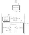
도 1은 본 발명의 실시 예들에 따른 구동 회로(10)를 보여준다. 도 1을 참조하면, 부하 회로(LC, Load Circuit)의 일단에 세팅 전압(VSET)이 공급된다. 세팅 전압(VSET)은 부하 회로(LC)의 내부 배선들에 충전하고자 하는 목표 전압일 수 있다. 구동 회로(10)는 충전 노드(CN, Charge Node)를 포함하는 도전선을 통해 부하 회로(LC)와 연결된다. 충전 노드(CN)를 포함하는 도전선은 세팅 전압(VSET)에 의해 충전될 부하 회로(LC)의 내부 배선들에 전기적으로 연결될 수 있다. 구동 회로(10)는 세팅 전압(VSET)의 소스와 충전 노드(CN)의 사이에서 부하 회로(LC)의 내부 배선들을 통해 전류가 흐르도록 강제할 수 있다. 예를 들어, 구동 회로(10)는 충전 노드(CN)로부터 전류를 유출하거나, 또는 충전 노드(CN)로 전류를 공급할 수 있다. 부하 회로(LC)의 내부 배선들을 통해 전류가 흐르도록 강제함으로써, 구동 회로(10)는 부하 회로(LC)의 내부의 배선들의 전압들이 세팅 전압(VSET)을 추종하는 속도를 향상시킬 수 있다.1 shows a
도 1을 참조하면, 구동 회로(10)는 클램프 스위치(CS, Clamp Switch), 충전 제어 회로(CCC, Charge Control Circuit), 그리고 충전 회로(CC, Charge Circuit)를 포함한다.Referring to FIG. 1, the
클램프 스위치(CS)는 충전 제어 회로(CCC)의 제어에 따라, 충전 회로(CC)가 충전 노드(CN)로부터 유출하는 전류량 또는 충전 회로(CC)가 충전 노드(CN)로 공급하는 전류량을 조절할 수 있다. 예를 들어, 클램프 스위치(CS)는 충전 제어 회로(CCC)로부터 공급되는 클램프 전압(VCLP)을 수신하는 게이트, 충전 회로(CC)와 연결된 제1 노드, 그리고 충전 노드(CN)와 연결된 제2 노드를 갖는 트랜지스터를 포함할(또는 구성될) 수 있다. 예를 들어, 클램프 스위치(CS)는 PMOS 타입 트랜지스터를 포함할(또는 구성될) 수 있다.The clamp switch CS controls the amount of current flowing out from the charging node CN or the amount of current supplied from the charging circuit CC to the charging node CN under the control of the charging control circuit CCC . For example, the clamp switch CS has a gate receiving the clamp voltage VCLP supplied from the charge control circuit CCC, a first node connected to the charging circuit CC and a second node connected to the charging node CN, (Or may be) configured with a transistor having a node. For example, the clamp switch CS may comprise (or be configured) a PMOS type transistor.
충전 제어 회로(CCC)는 클램프 전압(VCLP)을 조절함으로써, 클램프 스위치(CS)를 통해 충전 노드(CN) 또는 부하 회로(LC)로부터 유출(또는 드레인)되는 전류량 또는 충전 노드(CN) 또는 부하 회로(LC)로 공급(또는 유입)되는 전류량을 조절할 수 있다.The charge control circuit CCC adjusts the clamp voltage VCLP so that the amount of current flowing out (or drained) from the charge node CN or the load circuit LC through the clamp switch CS, The amount of current supplied (or introduced) to the circuit LC can be adjusted.
충전 회로(CC)는 방전 트랜지스터(DT, Discharge Transistor), 세팅 트랜지스터(ST, Set Transistor), 그리고 전류 소스(CS, Current Source)를 포함한다. 방전 트랜지스터(DT)는 클램프 스위치(CS) 및 접지 전압이 공급되는 접지 노드 사이에 연결된다. 방전 트랜지스터(DT)는 방전 활성 신호(EN_D)에 응답하여 동작한다. 방전 활성 신호(EN_D)는 부하 회로(LC)의 내부 배선들 또는 충전 노드(CN)를 방전할 때에 활성화될 수 있다. 방전 활성 신호(EN_D)가 활성화되면, 방전 트랜지스터(DT)는 턴-온 되고, 부하 회로(LC)의 내부 배선들 또는 충전 노드(CN)를 접지 노드와 연결할 수 있다.The charging circuit CC includes a discharging transistor DT, a setting transistor ST, and a current source CS. The discharge transistor DT is connected between the clamp switch CS and the ground node to which the ground voltage is supplied. The discharging transistor DT operates in response to the discharging enable signal EN_D. The discharging enable signal EN_D can be activated when discharging the internal wirings of the load circuit LC or the charging node CN. When the discharging enable signal EN_D is activated, the discharging transistor DT is turned on, and the internal wirings of the load circuit LC or the charging node CN can be connected to the ground node.
세팅 트랜지스터(ST) 및 전류 소스(CS)는 클램프 스위치(CS) 및 접지 노드 사이에 직렬 연결된다. 세팅 트랜지스터(ST)는 충전 활성 신호(EN_S)에 응답하여 동작한다. 충전 활성 신호(EN_S)가 활성화되면, 세팅 트랜지스터(ST)는 부하 회로(LC)의 내부 배선들 또는 충전 노드(CS)를 전류 소스(CS)와 연결할 수 있다. 도 1에서, 세팅 트랜지스터(ST)가 클램프 스위치(CS)의 쪽에 배치되고, 전류 소스(CS)가 접지 노드의 쪽에 배치되는 것으로 도시되어 있으나, 세팅 트랜지스터(ST) 및 전류 소스(CS)의 위치는 변경될 수 있다.The setting transistor ST and the current source CS are connected in series between the clamp switch CS and the ground node. The setting transistor ST operates in response to the charging activation signal EN_S. When the charging activation signal EN_S is activated, the setting transistor ST can connect the internal wirings of the load circuit LC or the charging node CS with the current source CS. 1, the setting transistor ST is arranged on the side of the clamp switch CS, and the current source CS is arranged on the side of the ground node. However, the setting transistor ST and the current source CS Can be changed.
또한, 방전 트랜지스터(DT)는 접지 노드와 연결되는 것으로 도시되어 있으나, 방전 트랜지스터(DT)는 접지 노드가 아닌 전압 노드에 연결될 수 있다. 예를 들어, 방전 트랜지스터(DT)는 전원 전압이 인가되는 전원 노드에 연결될 수 있다.Also, although the discharge transistor DT is shown as being connected to the ground node, the discharge transistor DT may be connected to a voltage node other than the ground node. For example, the discharge transistor DT may be connected to a power supply node to which a power supply voltage is applied.
상술된 바와 같이, 본 발명의 실시 예에 따른 구동 회로(10)는 부하 회로(LC)의 내부 배선들 또는 충전 노드(CN)로부터 전류를 유출하거나 또는 부하 회로(LC)의 내부 배선들 또는 충전 노드(CN)로 전류를 공급함으로써, 부하 회로(LC)의 내부 배선들 또는 충전 노드(CN)의 전압이 세팅 전압(VSET)을 추종하는 속도를 향상시킨다.As described above, the
도 1을 참조하여, 클램프 스위치(CS)가 PMOS 타입의 트랜지스터를 포함하는(또는 구성되는) 예가 설명되었다. 그러나, 본 발명의 기술적 사상은 클램프 스위치(CS)가 NMOS 타입의 트랜지스터를 포함하는(구성되는) 때에도 적용될 수 있다.Referring to Fig. 1, an example in which the clamp switch CS includes (or constitutes) a PMOS type transistor has been described. However, the technical idea of the present invention can also be applied when the clamp switch CS includes (constitutes) an NMOS type transistor.
도 2는 도 1의 구동 회로(10)의 응용 예(11)를 보여준다. 도 1과 비교하면, 도 2에서 구동 회로(11)의 충전 제어 회로(CCC1)가 더 상세하게 도시되어 있다. 도 2를 참조하면, 충전 제어 회로(CCC1)는 고정된 활성 레벨 및 고정된 비활성 레벨을 갖는 클램프 전압(VCMP)을 출력하는 전압원일 수 있다. 예를 들어, 충전 활성 신호(EN_S)가 활성화된 때에, 충전 제어 회로(CCC1)는 클램프 스위치(CS)를 턴-온할 수 있는 고정된 레벨을 가진 전압을 클램프 전압(VCLP)으로 출력할 수 있다. 충전 활성 신호(EN_S)가 비활성화된 때에, 충전 제어 회로(CCC1)는 클램프 스위치(CS)를 턴-오프할 수 있는 고정된 레벨을 가진 전압을 클램프 전압(VCLP)으로 출력할 수 있다.Fig. 2 shows an application example 11 of the
도 2에 도시된 구동 회로(11)에서, 부하 회로(LC)의 내부 배선들 또는 충전 노드(CN)를 충전할 때에, 클램프 전압(VCLP)은 고정된 레벨을 갖는다. 부하 회로(LC)의 내부 배선들 또는 충전 노드(CN)의 전압이 세팅 전압(VSET)에 근접할수록, 구동 회로(11)의 구동 능력, 즉 공급 또는 유출하는 전류량이 감소한다. 따라서, 부하 회로(LC)의 내부 배선들 또는 충전 노드(CN)의 충전을 세팅 전압(VSET)까지 완료하는 데에 상대적으로 긴 시간이 소요된다는 문제가 있다.In the driving
도 3은 도 1의 구동 회로(10)의 다른 응용 예(12)를 보여준다. 도 1과 비교하면, 도 3에서 구동 회로(12)의 충전 제어 회로(CCC2)가 더 상세하게 도시되어 있다. 도 3을 참조하면, 충전 제어 회로(CCC2)는 증폭기(AP)를 포함한다. 증폭기(AP)의 양의 입력에 기준 전압(VREF)이 공급된다. 증폭기(AP)의 음의 입력은 충전 노드(CN)에 연결된다. 증폭기(AP)의 출력은 클램프 전압(VCLP)으로서 클램프 스위치(CS)의 게이트에 전달된다.Fig. 3 shows another
충전이 시작될 때의 초기 상태에서, 충전 노드(CN) 또는 부하 회로(LC)의 내부 배선들의 전압들이 기준 전압(VREF)보다 높을 수 있다. 증폭기(AP)는 음의 레벨을 갖는 클램프 전압(VCLP)을 클램프 스위치(CS)의 게이트에 인가할 수 있다. 충전 노드(CN) 또는 부하 회로(LC)의 내부 배선들의 전압들이 기준 전압(VREF)보다 더 높을수록, 증폭기(AP)는 더 낮은 음의 레벨을 갖는 클램프 전압(VCLP)을 클램프 스위치(CS)의 게이트에 인가하며, 따라서 클램프 스위치(CS)는 더 많은 양의 전류를 부하 회로(LC)의 내부 배선들 및 충전 노드(CN)를 통해 흐르도록 강제할 수 있다.In the initial state when the charging starts, the voltages of the internal wirings of the charging node CN or the load circuit LC may be higher than the reference voltage VREF. The amplifier AP can apply the clamp voltage VCLP having a negative level to the gate of the clamp switch CS. The amplifier AP supplies the clamp voltage VCLP having a lower negative level to the clamp switch CS as the voltages of the internal wirings of the charging node CN or the load circuit LC are higher than the reference voltage VREF, So that the clamp switch CS can force a larger amount of current to flow through the internal wiring of the load circuit LC and the charging node CN.
증폭기(AP)의 이득(gain)으로 인해, 기준 전압(VREF)과 부하 회로(LC)의 내부 배선들 또는 충전 노드(CN)의 전압들의 차이가 증폭되어 클램프 전압(VCLP)에 반영된다. 따라서, 증폭기(AP)의 이득(gain)에 의해 클램프 스위치(CS)를 통과하는 전류량이 강화(또는 증폭)되며, 구동 회로(12)의 구동 능력이 향상된다.Due to the gain of the amplifier AP, the difference between the reference voltages VREF and the internal wiring of the load circuit LC or the voltages of the charging node CN is amplified and reflected in the clamp voltage VCLP. Therefore, the amount of current passing through the clamp switch CS is strengthened (or amplified) by the gain of the amplifier AP, and the driving ability of the driving
부하 회로(LC)의 내부 배선들 또는 충전 노드(CN)의 전압이 감소하여 기준 전압(VREF)에 도달하면, 증폭기(AP)는 접지 또는 양의 출력을 클램프 스위치(CS)에 전달하며, 따라서 클램프 스위치(CS)는 턴-오프 된다.When the internal wiring of the load circuit LC or the voltage of the charging node CN is reduced to reach the reference voltage VREF, the amplifier AP transfers the ground or positive output to the clamp switch CS, The clamp switch CS is turned off.
상술된 바와 같이, 충전 제어 회로(CCC2)에 증폭기(AP)가 사용되면, 증폭기(AP)의 이득으로 인해 클램프 스위치(CS)를 통과하는 전류량이 증폭된다. 따라서, 구동 회로(12)의 구동 능력이 향상된다. 또한, 증폭기(AP)가 충전 노드(CN) 및 클램프 스위치(CS)와 피드백 루프를 형성하면, 증폭기(AP)에 의해 충전 노드(CN)의 전압이 기준 전압(VREF)의 레벨로 조절된다. 즉, 기준 전압(VREF)이 세팅 전압(VSET) 또는 그와 유사한 레벨로 설정되면, 구동 회로(12)는 충전 노드(CN) 또는 부하 회로(LC)의 내부 배선들의 전압이 세팅 전압(VSET) 또는 그와 유사한 레벨을 추종하는 것을 지원한다.As described above, when the amplifier AP is used in the charge control circuit CCC2, the amount of current passing through the clamp switch CS is amplified due to the gain of the amplifier AP. Therefore, the driving ability of the driving
그러나, 도 3에 도시된 바와 같이 충전 제어 회로(CCC2)에 증폭기(AP)가 사용되면, 충전 제어 회로(CCC2)의 복잡도가 증가하고, 소비 전류 및 면적이 증가하는 문제가 있다.However, if the amplifier (AP) is used in the charge control circuit (CCC2) as shown in Fig. 3, the complexity of the charge control circuit (CCC2) increases and the consumption current and area increase.
도 4는 충전 제어 회로(CCC2)의 증폭기(AP)의 예를 보여주는 회로도이다. 도 4를 참조하면, 증폭기(AP)는 제1 내지 제8 트랜지스터들(T1~T8)을 포함한다.4 is a circuit diagram showing an example of an amplifier (AP) of the charge control circuit (CCC2). Referring to FIG. 4, the amplifier AP includes first through eighth transistors T1 through T8.
제1 트랜지스터(T1)는 증폭 활성 반전신호(/EN_A)가 공급되는 게이트, 클램프 스위치(CS)에 연결되는 제1 노드, 그리고 접지 노드에 연결되는 제2 노드를 갖는다. 제2 트랜지스터(T2)는 제3 트랜지스터(T3)의 게이트와 연결되는 게이트, 클램프 스위치(CS)와 연결되는 제1 노드, 그리고 접지 노드와 연결되는 제2 노드를 갖는다. 제1 트랜지스터(T1) 및 제2 트랜지스터(T2)는 병렬 연결된다.The first transistor T1 has a gate to which the amplifying active inverted signal / EN_A is supplied, a first node connected to the clamp switch CS, and a second node connected to the ground node. The second transistor T2 has a gate connected to the gate of the third transistor T3, a first node connected to the clamp switch CS, and a second node connected to the ground node. The first transistor T1 and the second transistor T2 are connected in parallel.
제3 트랜지스터(T3)는 제2 트랜지스터(T2)의 게이트와 연결되는 게이트, 제3 트랜지스터(T3)의 게이트와 연결되어 다이오드 연결을 형성하는 제1 노드, 그리고 접지 노드와 연결되는 제2 노드를 갖는다. 제4 트랜지스터(T4)는 증폭 활성 반전 신호(/EN_A)가 공급되는 게이트, 제3 트랜지스터(T3)와 제1 노드와 연결되는 제1 노드, 그리고 접지 노드와 연결되는 제2 노드를 갖는다.The third transistor T3 has a gate connected to the gate of the second transistor T2, a first node connected to the gate of the third transistor T3 to form a diode connection, and a second node connected to the ground node . The fourth transistor T4 has a gate to which the amplifying enable signal / EN_A is supplied, a third transistor T3, a first node connected to the first node, and a second node connected to the ground node.
제5 트랜지스터(T5)는 기준 전압(VREF)이 공급되는 게이트, 제7 트랜지스터(T7)의 제2 노드와 연결되는 제1 노드, 그리고 클램프 스위치(CS)와 연결되는 제2 노드를 갖는다. 제6 트랜지스터(T6)는 충전 노드(CN)와 연결되는 게이트, 제7 트랜지스터(T7)의 제2 노드와 연결되는 제1 노드, 그리고 제3 트랜지스터(T3)의 제1 노드와 연결되는 제2 노드를 갖는다.The fifth transistor T5 has a gate to which the reference voltage VREF is supplied, a first node connected to the second node of the seventh transistor T7, and a second node connected to the clamp switch CS. The sixth transistor T6 has a gate connected to the charge node CN, a first node connected to the second node of the seventh transistor T7, and a second node connected to the first node of the third transistor T3. Node.
제7 트랜지스터(T7)는 증폭 활성 반전 신호(/EN_A)가 공급되는 게이트, 제8 트랜지스터(T8)의 제2 노드와 연결되는 제1 노드, 그리고 제5 트랜지스터(T5)의 제1 노드와 연결되는 제2 노드를 갖는다. 제8 트랜지스터(T8)는 바이어스 전압(BIAS)이 공급되는 게이트, 전원 전압(VCC)이 공급되는 전원 노드와 연결되는 제1 노드, 그리고 제7 트랜지스터(T7)의 제1 노드와 연결되는 제2 노드를 갖는다.The seventh transistor T7 has a gate to which the amplification enable signal / EN_A is supplied, a first node connected to the second node of the eighth transistor T8, and a first node connected to the first node of the fifth transistor T5. Lt; / RTI > The eighth transistor T8 includes a gate to which the bias voltage BIAS is supplied, a first node connected to the power supply node to which the power supply voltage VCC is supplied, and a second node connected to the first node of the seventh transistor T7. Node.
예시적으로, 제1 내지 제4 트랜지스터들(T1~T4)은 NMOS 타입이고, 제5 내지 제8 트랜지스터들(T5~T8)은 PMOS 타입일 수 있다.Illustratively, the first to fourth transistors T1 to T4 may be NMOS transistors and the fifth to eighth transistors T5 to T8 may be PMOS transistors.
제1 트랜지스터(T1), 제4 트랜지스터(T4), 그리고 제7 트랜지스터(T7)는 증폭기(AP)의 활성화 또는 비활성화를 결정할 수 있다. 증폭기(AP)가 활성화될 때에, 증폭 활성 반전 신호(/EN_A)는 로우 레벨을 갖는다. 제1 트랜지스터(T1) 및 제4 트랜지스터(T4)는 턴-오프 되고, 제7 트랜지스터(T7)는 턴-온 된다.The first transistor T1, the fourth transistor T4 and the seventh transistor T7 can determine whether to activate or deactivate the amplifier AP. When the amplifier AP is activated, the amplification active inverted signal / EN_A has a low level. The first transistor T1 and the fourth transistor T4 are turned off and the seventh transistor T7 is turned on.
제2 트랜지스터(T2), 제3 트랜지스터(T3), 제5 트랜지스터(T5) 및 제6 트랜지스터(T6)는 차동 증폭기를 형성할 수 있다. 제8 트랜지스터(T8)는 바이어스 전압(BIAS)에 따라 증폭기(AP) 내부에서 흐르는 전류량을 조절하는 전류 제어기로 기능할 수 있다.The second transistor T2, the third transistor T3, the fifth transistor T5 and the sixth transistor T6 may form a differential amplifier. The eighth transistor T8 may function as a current controller for adjusting the amount of current flowing in the amplifier AP according to the bias voltage BIAS.
증폭기(AP)가 비활성화될 때에, 증폭 활성 반전 신호(/EN_A)는 하이 레벨을 갖는다. 제7 트랜지스터(T7)는 턴-오프 되어, 전류 경로를 차단한다. 제1 트랜지스터(T1)는 턴-온 되어, 클램프 스위치(CS)에 접지 노드를 연결한다. 제4 트랜지스터(T4)는 턴-오프 되어, 제3 트랜지스터(T3)의 제1 노드에 접지 노드를 연결한다.When the amplifier AP is inactivated, the amplification active inverted signal / EN_A has a high level. The seventh transistor T7 is turned off to cut off the current path. The first transistor T1 is turned on and connects the ground node to the clamp switch CS. The fourth transistor T4 is turned off to connect the ground node to the first node of the third transistor T3.
도 3 및 도 4를 참조하면, 충전 제어 회로(CCC2)에 증폭기(AP)를 사용하기 위해, 적어도 8개의 트랜지스터들이 요구된다. 따라서, 구동 회로(12)의 복잡도 및 면적이 증가한다. 또한, 증폭기(AP)는 제5 트랜지스터(T5)를 통한 제1 전류 경로와 제6 트랜지스터(T6)를 통한 제2 전류 경로를 갖는다. 두 개의 전류 경로들을 통해 전류가 소비되므로, 구동 회로(12)의 소비 전류가 증가한다.Referring to Figures 3 and 4, in order to use an amplifier (AP) in the charge control circuit (CCC2), at least eight transistors are required. Thus, the complexity and area of the driving
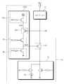
도 5는 도 1의 구동 회로(10)의 다른 응용 예(13)를 보여준다. 도 1과 비교하면, 도 5에서 구동 회로(13)의 충전 제어 회로(CCC3)가 더 상세하게 도시되어 있다. 도 5를 참조하면, 충전 제어 회로(CCC3)는 바이어스 회로(BC), 활성 스위치(ES), 단일 스테이지 증폭기(SSA, Single Stage Amplifier), 그리고 비교 전압 생성기(CVG, Comparison Voltage Generator)를 포함한다.Fig. 5 shows another
바이어스 회로(BC)는 클램프 스위치(CS)의 게이트에 연결된다. 바이어스 회로(BC)는 바이어스 전압(BIAS)에 응답하여, 비교 전압 생성기(CVG), 단일 스테이지 증폭기(SSA) 및 클램프 스위치(CS)의 게이트를 통해 접지 전압이 공급되는 접지 노드로 흐르는 전류량을 조절하도록 구성될 수 있다. 예를 들어, 바이어스 회로(BC)는 바이어스 전압(BIAS)에 응답하여 전류를 출력하는 전류 소스로 기능할 수 있다. 바이어스 회로(BC)는 클램프 스위치(CS)의 게이트 및 접지 노드 사이에 연결되며, 바이어스 전압(BIAS)에 의해 조절되는 트랜지스터를 포함할(또는 구성될) 수 있다. 예를 들어, 바이어스 회로(BIAS)는 NMOS 타입의 트랜지스터를 포함할(또는 구성될) 수 있다.The bias circuit BC is connected to the gate of the clamp switch CS. The bias circuit BC controls the amount of current flowing to the ground node supplied with the ground voltage through the gates of the comparison voltage generator CVG, the single stage amplifier SSA and the clamp switch CS in response to the bias voltage BIAS. . For example, the bias circuit BC may function as a current source that outputs current in response to the bias voltage BIAS. The bias circuit BC is connected between the gate and the ground node of the clamp switch CS and may include (or be configured to be) a transistor that is regulated by the bias voltage BIAS. For example, the bias circuit BIAS may include (or be configured to be) an NMOS type transistor.
활성 스위치(ES)는 바이어스 회로(BC) 및 단일 스테이지 증폭기(SSA)의 사이에 연결된다. 활성 스위치(ES)는 충전 제어 회로(CCC3)의 활성화 또는 비활성화를 결정할 수 있다. 활성 스위치(ES)는 바이어스 회로(BC) 및 단일 스테이지 증폭기(SSA) 사이에 연결되며, 증폭 활성 신호(EN_A)에 응답하여 동작하는 트랜지스터를 포함할(또는 구성될) 수 있다. 증폭 활성 신호(EN_A)가 활성화된 때에, 활성 스위치(ES)의 트랜지스터는 턴-온 되고, 충전 제어 회로(CCC3)가 활성화될 수 있다. 증폭 활성 신호(EN_A)가 비활성화된 때에, 활성 스위치(ES)의 트랜지스터는 턴-오프 되고, 충전 제어 회로(CCC3)가 비활성화될 수 있다. 예를 들어, 활성 스위치(ES)는 PMOS 타입의 트랜지스터를 포함할(또는 구성될) 수 있다.The active switch ES is connected between the bias circuit BC and the single stage amplifier SSA. The activation switch ES can determine activation or deactivation of the charge control circuit CCC3. The active switch ES is connected between the bias circuit BC and the single stage amplifier SSA and may include (or be configured to be) a transistor that operates in response to the amplification enable signal EN_A. When the amplification enable signal EN_A is activated, the transistor of the active switch ES is turned on and the charge control circuit CCC3 can be activated. When the amplification enable signal EN_A is deactivated, the transistor of the active switch ES is turned off and the charge control circuit CCC3 can be deactivated. For example, the active switch ES may comprise (or be comprised of) a transistor of the PMOS type.
단일 스테이지 증폭기(SSA)는 비교 전압 생성기(CVG) 및 활성 스위치(ES)의 사이에 연결된다. 단일 스테이지 증폭기(SSA)는 비교 전압 생성기(CVG)로부터 출력되는 비교 전압(VCOM)과 충전 노드(CN)의 전압의 차이를 증폭하여 활성 스위치(ES)를 통해 클램프 전압(VCLP)으로 출력할 수 있다. 예를 들어, 단일 스테이지 증폭기(SSA)는 충전 노드(CN)에 연결되는 게이트, 비교 전압 생성기(CVG)로부터 비교 전압(VCOM)을 수신하는 제1 노드, 그리고 활성 스위치(ES)를 통해 클램프 전압(VCLP)을 출력하는 제2 노드를 갖는 트랜지스터를 포함할(또는 구성될) 수 있다. 예를 들어, 단일 스테이지 증폭기(SSA)는 PMOS 타입의 트랜지스터를 포함할(또는 구성될) 수 있다.A single stage amplifier (SSA) is connected between the comparison voltage generator (CVG) and the active switch (ES). The single stage amplifier SSA amplifies the difference between the voltage of the comparison node VCOM output from the comparison voltage generator CVG and the voltage of the charging node CN and outputs the amplified difference to the clamp voltage VCLP via the active switch ES have. For example, the single stage amplifier SSA includes a gate connected to the charging node CN, a first node receiving the comparison voltage VCOM from the comparison voltage generator CVG, (Or be configured) a transistor having a second node outputting a first reference voltage (VCLP). For example, a single stage amplifier (SSA) may include (or be comprised of) PMOS type transistors.
비교 전압 생성기(CVG)는 기준 전압(VREF)에 따라 결정되는 비교 전압(VCOM)을 출력할 수 있다. 비교 전압 생성기(CVG)는 기준 전압(VREF)이 공급되는 게이트, 전원 전압(VCC)이 공급되는 전원 노드와 연결되는 제1 노드, 그리고 비교 전압(VCOM)을 출력하는 제2 노드를 갖는 트랜지스터를 포함할(또는 구성될) 수 있다. 예를 들어, 비교 전압 생성기(CVG)는 NMOS 타입의 트랜지스터를 포함할(또는 구성될) 수 있다.The comparison voltage generator CVG can output the comparison voltage VCOM determined according to the reference voltage VREF. The comparison voltage generator CVG includes a transistor having a gate to which a reference voltage VREF is supplied, a first node connected to a power supply node supplied with a power supply voltage VCC, and a second node outputting a comparison voltage VCOM May be included (or configured). For example, the comparison voltage generator CVG may include (or be configured to be) an NMOS type transistor.
구동 회로(13)는 부하 회로(LC)의 내부 배선들 또는 충전 노드(CN)의 전압을 현재 전압보다 낮은 전압으로 구동할 수 있다. 이하에서, 구동 회로(13)의 동작이 더 상세하게 설명된다.The driving
구동 회로(13)가 활성화되면, 활성 스위치(ES)는 턴-온 된다. 간결한 설명을 위하여, 이후의 설명에서 활성 스위치(ES)에 대한 설명은 제외된다. 바이어스 회로(BC)는 일정한 전류를 흐르게 하는 전류 소스로 기능할 수 있다. 비교 전압 생성기(CVG)는 기준 전압(VREF)과 비교하여 비교 전압 생성기(CVG)의 트랜지스터의 문턱 전압만큼 낮은 전압을 비교 전압(VCOM)으로 출력한다.When the driving
단일 스테이지 증폭기(SSA)의 제1 노드에 비교 전압(VCOM)이 공급되고, 제2 노드에 전류 소스로 기능하는 바이어스 회로(BC)가 연결되어 있으므로, 단일 스테이지 증폭기(SSA)는 공통 소스 증폭기(common source amplifier)로 기능할 수 있다. 단일 스테이지 증폭기(SSA)는 음의 이득(gain)을 가질 수 있다. 단일 스테이지 증폭기(SSA)는 비교 전압(VCOM)과 충전 노드(CN)의 전압의 차이를 음의 이득으로 증폭하여 클램프 전압(VCLP)으로 출력할 수 있다.Stage amplifier (SSA) is connected to the common source amplifier (SSB) because the comparison voltage VCOM is supplied to the first node of the single stage amplifier SSA and the bias circuit BC is connected to the second node, common source amplifier). A single stage amplifier (SSA) may have a negative gain. The single stage amplifier SSA can amplify the difference between the voltage of the comparison voltage VCOM and the voltage of the charging node CN with a negative gain and output it as the clamp voltage VCLP.
충전이 시작될 때의 초기 상태에서, 충전 노드(CN) 또는 부하 회로(LC)의 내부 배선들의 전압들은 비교 전압(VCOM)보다 높을 수 있다. 따라서, 단일 스테이지 증폭기(SSA)는 충전 노드(CN)의 전압과 비교 전압(VCOM) 사이의 차이보다 큰 절대값(즉, 증폭된 값) 및 음의 부호를 갖는 전압을 클램프 전압(VCLP)으로 출력할 수 있다. 클램프 전압(VCLP)에 의해 클램프 스위치(CS)는 턴-온 되고, 충전 회로(CC)에 의해 부하 회로(LC) 및 충전 노드(CN)를 통해 전류가 흐른다. 즉, 부하 회로(LC)의 내부 배선들 및 충전 노드(CN)의 전압이 세팅 전압(VSET)을 향해 점차 감소한다.In the initial state at the start of charging, the voltages of the internal wirings of the charging node CN or the load circuit LC may be higher than the comparison voltage VCOM. Thus, the single stage amplifier SSA is capable of amplifying the voltage having the negative sign and the absolute value (i.e., the amplified value) larger than the difference between the voltage of the charging node CN and the comparison voltage VCOM to the clamp voltage VCLP Can be output. The clamp switch CS is turned on by the clamp voltage VCLP and the current flows through the load circuit LC and the charge node CN by the charge circuit CC. That is, the voltage of the internal wirings of the load circuit LC and the charging node CN gradually decreases toward the set voltage VSET.
부하 회로(LC)의 내부 배선들 및 충전 노드(CN)의 전압들이 감소함에 따라, 비교 전압(VCOM)과 충전 노드(CN)의 전압의 차이가 점차 감소한다. 충전 노드(CN)의 전압이 비교 전압(VCOM)과 비교하여 단일 스테이지 증폭기(SSA)의 문턱 전압만큼 낮은 전압에 도달하면, 단일 스테이지 증폭기(SSA)는 접지 레벨 또는 양의 레벨을 갖는 클램프 전압(VCLP)을 출력한다. 따라서, 클램프 스위치(CS)가 턴-오프 된다. 즉, 구동 회로(15)는 충전 노드(CN)의 전압이 기준 전압(VREF)보다 비교 전압 생성기(CVG)의 트랜지스터의 문턱 전압 및 단일 스테이지 증폭기(SSA)의 트랜지스터의 문턱 전압만큼 낮은 전압을 추종하도록 제어한다. 따라서, 기준 전압(VREF)이 세팅 전압(VSET)과 비교하여 단일 스테이지 증폭기(SSA)의 트랜지스터의 문턱 전압 및 비교 전압 생성기(CVG)의 트랜지스터의 문턱 전압만큼 높은 전압으로 설정되면, 구동 회로(13)는 충전 노드(CN) 또는 부하 회로(LC)의 내부 배선들의 전압들을 세팅 전압(VSET) 또는 그와 유사한 레벨의 전압으로 구동한다. 특히, 클램프 스위치(CS)의 구동은 증폭기, 더 상세하게는 단일 스테이지 증폭기(SSA)에 의해 수행되므로, 구동 회로(13)의 구동 능력이 향상된다.As the voltages of the internal wirings of the load circuit LC and the charging node CN decrease, the difference between the voltages of the comparison voltage VCOM and the charging node CN gradually decreases. When the voltage of the charging node CN reaches a voltage as low as the threshold voltage of the single stage amplifier SSA as compared with the comparison voltage VCOM, the single stage amplifier SSA outputs a clamp voltage having a ground level or a positive level VCLP). Thus, the clamp switch CS is turned off. That is, the driving
도 4의 비교기(AP)와 비교하면, 도 5의 충전 제어 회로(CCC3)는 더 적은 수의 트랜지스터들을 이용하여, 기준 전압(VREF)을 이용하여 목표 레벨을 설정하고 이득(gain)을 통해 구동 능력을 향상시키는 동일한 효과를 제공한다. 특히, 도 5의 충전 제어 회로(CCC3)는 하나의 전류 경로만을 사용함으로써, 도 4의 증폭기(AP)와 대비하여 1/5의 전류만을 소비하는 것으로 관측된다. 즉, 도 5의 충전 제어 회로(CCC3)가 사용되면, 목표 레벨을 설정하는 기능 및 구동 능력을 향상시키는 효과를 유지하면서, 감소된 복잡도, 감소된 소비 전력, 그리고 감소된 면적을 차지하는 구동 회로(13)가 제공된다.Compared with the comparator AP of FIG. 4, the charge control circuit CCC3 of FIG. 5 uses a smaller number of transistors to set the target level using the reference voltage VREF and to drive through the gain Provide the same effect of improving the ability. In particular, it is observed that the charge control circuit CCC3 of FIG. 5 consumes only 1/5 of the current compared with the amplifier AP of FIG. 4 by using only one current path. That is, when the charge control circuit (CCC3) of Fig. 5 is used, the driving circuit which occupies the reduced complexity, the reduced power consumption, and the reduced area while maintaining the effect of improving the target level setting function and the driving
도 6은 도 5의 구동 회로(13)의 응용 예(14)를 보여준다. 도 5와 비교하면, 도 6에서 부하 회로(LC)에 세팅 전압(VSET)이 인가되지 않고, 세팅 전압 생성기(SVG)가 구동 회로(14)의 내부에 더 포함된다. 세팅 전압 생성기(SVG)는 세팅 전압(VSET)을 공급하는 전압 노드 및 트랜지스터를 포함한다. 트랜지스터는 세팅 활성 신호(EN_S)에 응답하여, 세팅 전압(VSET)을 출력할 수 있다. 예를 들어, 충전 노드(CN) 또는 부하 회로(LC)의 내부 배선들을 세팅 전압(VSET)으로 세팅할 때에, 세팅 활성 신호(EN_S)가 활성화되고, 세팅 전압 생성기(SVG)의 트랜지스터가 턴-온될 수 있다.Fig. 6 shows an application example 14 of the
도 6에서, 세팅 전압 생성기(SVG)는 클램프 스위치(CS) 및 충전 회로(CC) 사이의 노드에 세팅 전압(VSET)을 공급하는 것으로 도시되어 있다. 그러나, 세팅 전압 생성기(SVG)는 구동 회로(14)의 내에서, 충전 노드(CN)와 전기적으로 연결되는 임의의 노드에 세팅 전압(VSET)을 공급하도록 변경될 수 있다. 예를 들어, 세팅 전압 생성기(SVG)는 충전 노드(CN)와 클램프 스위치(CS) 사이의 노드, 또는 충전 노드(CN)에 직접 세팅 전압(VSET)을 공급하도록 응용될 수 있다.In Fig. 6, the setting voltage generator SVG is shown as supplying the setting voltage VSET to the node between the clamp switch CS and the charging circuit CC. However, the setting voltage generator SVG may be modified within the driving
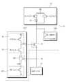
도 7은 도 5의 구동 회로(13)를 다른 타입으로 응용한 예(15)를 보여준다. 예시적으로, 도 5의 구동 회로(13)는 PMOS 타입이고, 도 7의 구동 회로(15)는 NMOS 타입일 수 있다. 도 5의 구동 회로(13)의 클램프 스위치(CS)는 PMOS 트랜지스터인 반면, 도 7의 구동 회로(13)의 클램프 스위치(CS)는 NMOS 트랜지스터일 수 있다. 또한, 도 7의 구동 회로(13)의 충전 제어 회로(CCC4)는 도 5의 구동 회로(13)의 충전 제어 회로(CCC3)와 다소 상이한 구성을 가질 수 있다.Fig. 7 shows an example (15) in which the driving
도 5의 충전 회로(CC)와 비교하면, 도 7의 충전 회로(CC')는 방전 트랜지스터(DT, Discharge Transistor), 세팅 트랜지스터(ST, Set Transistor), 그리고 전류 소스(CS, Current Source)를 포함한다. 방전 트랜지스터(DT)는 클램프 스위치(CS) 및 전원 전압이 공급되는 전원 노드 사이에 연결된다. 방전 트랜지스터(DT)는 방전 활성 신호(EN_D)에 응답하여 동작한다. 방전 활성 신호(EN_D)는 부하 회로(LC)의 내부 배선들 또는 충전 노드(CN)를 방전할 때에 활성화될 수 있다. 방전 활성 신호(EN_D)가 활성화되면, 방전 트랜지스터(DT)는 턴-온 되고, 부하 회로(LC)의 내부 배선들 또는 충전 노드(CN)를 접지 노드와 연결할 수 있다.Compared with the charging circuit CC of FIG. 5, the charging circuit CC 'of FIG. 7 includes a discharging transistor DT, a setting transistor ST, and a current source CS . The discharge transistor DT is connected between the clamp switch CS and the power supply node to which the power supply voltage is supplied. The discharging transistor DT operates in response to the discharging enable signal EN_D. The discharging enable signal EN_D can be activated when discharging the internal wirings of the load circuit LC or the charging node CN. When the discharging enable signal EN_D is activated, the discharging transistor DT is turned on, and the internal wirings of the load circuit LC or the charging node CN can be connected to the ground node.
세팅 트랜지스터(ST) 및 전류 소스(CS)는 클램프 스위치(CS) 및 접지 노드 사이에 직렬 연결된다. 세팅 트랜지스터(ST)는 충전 활성 신호(EN_S)에 응답하여 동작한다. 충전 활성 신호(EN_S)가 활성화되면, 세팅 트랜지스터(ST)는 부하 회로(LC)의 내부 배선들 또는 충전 노드(CS)를 전류 소스(CS)와 연결할 수 있다. 도 7에서, 세팅 트랜지스터(ST)가 전원 노드의 쪽에 배치되고, 전류 소스(CS)가 클램프 스위치(CS)의 쪽에 배치되는 것으로 도시되어 있으나, 세팅 트랜지스터(ST) 및 전류 소스(CS)의 위치는 변경될 수 있다.The setting transistor ST and the current source CS are connected in series between the clamp switch CS and the ground node. The setting transistor ST operates in response to the charging activation signal EN_S. When the charging activation signal EN_S is activated, the setting transistor ST can connect the internal wirings of the load circuit LC or the charging node CS with the current source CS. 7, the setting transistor ST is arranged on the side of the power source node and the current source CS is on the side of the clamp switch CS. However, the setting transistor ST and the current source CS Can be changed.
또한, 방전 트랜지스터(DT)는 전원 노드와 연결되는 것으로 도시되어 있으나, 방전 트랜지스터(DT)는 전원 노드가 아닌 전압 노드에 연결될 수 있다. 예를 들어, 방전 트랜지스터(DT)는 접지 전압이 인가되는 접지 노드에 연결될 수 있다.Also, although the discharge transistor DT is shown connected to the power supply node, the discharge transistor DT may be connected to a voltage node other than the power supply node. For example, the discharge transistor DT may be connected to a ground node to which a ground voltage is applied.
도 7을 참조하면, 충전 제어 회로(CCC4)는 바이어스 회로(BC), 활성 스위치(ES), 단일 스테이지 증폭기(SSA, Single Stage Amplifier), 그리고 비교 전압 생성기(CVG, Comparison Voltage Generator)를 포함한다.7, the charge control circuit CCC4 includes a bias circuit BC, an active switch ES, a single stage amplifier (SSA), and a comparison voltage generator (CVG) .
바이어스 회로(BC)는 클램프 스위치(CS)의 게이트에 연결된다. 바이어스 회로(BC)는 바이어스 전압(BIAS)에 응답하여, 비교 전압 생성기(CVG), 단일 스테이지 증폭기(SSA) 및 클램프 스위치(CS)의 게이트를 통해 접지 전압이 공급되는 접지 노드로 흐르는 전류량을 조절하도록 구성될 수 있다. 예를 들어, 바이어스 회로(BC)는 바이어스 전압(BIAS)에 응답하여 전류를 출력하는 전류 소스로 기능할 수 있다. 바이어스 회로(BC)는 클램프 스위치(CS)의 게이트 및 전원 전압(VCC)이 공급되는 전원 노드 사이에 연결되며, 바이어스 전압(BIAS)에 의해 조절되는 트랜지스터를 포함할(또는 구성될) 수 있다. 예를 들어, 바이어스 회로(BIAS)는 PMOS 타입의 트랜지스터를 포함할(또는 구성될) 수 있다.The bias circuit BC is connected to the gate of the clamp switch CS. The bias circuit BC controls the amount of current flowing to the ground node supplied with the ground voltage through the gates of the comparison voltage generator CVG, the single stage amplifier SSA and the clamp switch CS in response to the bias voltage BIAS. . For example, the bias circuit BC may function as a current source that outputs current in response to the bias voltage BIAS. The bias circuit BC may include (or be configured to be) a transistor which is connected between the gate of the clamp switch CS and the power supply node to which the power supply voltage VCC is supplied, and is regulated by the bias voltage BIAS. For example, the bias circuit BIAS may include (or be configured) a transistor of the PMOS type.
활성 스위치(ES)는 바이어스 회로(BC) 및 단일 스테이지 증폭기(SSA)의 사이에 연결된다. 활성 스위치(ES)는 충전 제어 회로(CCC4)의 활성화 또는 비활성화를 결정할 수 있다. 활성 스위치(ES)는 바이어스 회로(BC) 및 단일 스테이지 증폭기(SSA) 사이에 연결되며, 증폭 활성 신호(EN_A)에 응답하여 동작하는 트랜지스터를 포함할(또는 구성될) 수 있다. 증폭 활성 신호(EN_A)가 활성화된 때에, 활성 스위치(ES)의 트랜지스터는 턴-온 되고, 충전 제어 회로(CCC3)가 활성화될 수 있다. 증폭 활성 신호(EN_A)가 비활성화된 때에, 활성 스위치(ES)의 트랜지스터는 턴-오프 되고, 충전 제어 회로(CCC3)가 비활성화될 수 있다. 예를 들어, 활성 스위치(ES)는 NMOS 타입의 트랜지스터를 포함할(또는 구성될) 수 있다.The active switch ES is connected between the bias circuit BC and the single stage amplifier SSA. The activation switch ES can determine activation or deactivation of the charge control circuit CCC4. The active switch ES is connected between the bias circuit BC and the single stage amplifier SSA and may include (or be configured to be) a transistor that operates in response to the amplification enable signal EN_A. When the amplification enable signal EN_A is activated, the transistor of the active switch ES is turned on and the charge control circuit CCC3 can be activated. When the amplification enable signal EN_A is deactivated, the transistor of the active switch ES is turned off and the charge control circuit CCC3 can be deactivated. For example, the active switch ES may comprise (or be configured) an NMOS type transistor.
단일 스테이지 증폭기(SSA)는 비교 전압 생성기(CVG) 및 활성 스위치(ES)의 사이에 연결된다. 단일 스테이지 증폭기(SSA)는 비교 전압 생성기(CVG)로부터 출력되는 비교 전압(VCOM)과 충전 노드(CN)의 전압의 차이를 증폭하여 활성 스위치(ES)를 통해 클램프 전압(VCLP)으로 출력할 수 있다. 예를 들어, 단일 스테이지 증폭기(SSA)는 충전 노드(CN)에 연결되는 게이트, 비교 전압 생성기(CVG)로부터 비교 전압(VCOM)을 수신하는 제1 노드, 그리고 활성 스위치(ES)를 통해 클램프 전압(VCLP)을 출력하는 제2 노드를 갖는 트랜지스터를 포함할(또는 구성될) 수 있다. 예를 들어, 단일 스테이지 증폭기(SSA)는 NMOS 타입의 트랜지스터를 포함할(또는 구성될) 수 있다.A single stage amplifier (SSA) is connected between the comparison voltage generator (CVG) and the active switch (ES). The single stage amplifier SSA amplifies the difference between the voltage of the comparison node VCOM output from the comparison voltage generator CVG and the voltage of the charging node CN and outputs the amplified difference to the clamp voltage VCLP via the active switch ES have. For example, the single stage amplifier SSA includes a gate connected to the charging node CN, a first node receiving the comparison voltage VCOM from the comparison voltage generator CVG, (Or be configured) a transistor having a second node outputting a first reference voltage (VCLP). For example, a single stage amplifier (SSA) may include (or be comprised of) an NMOS type transistor.
비교 전압 생성기(CVG)는 기준 전압(VREF)에 따라 결정되는 비교 전압(VCOM)을 출력할 수 있다. 비교 전압 생성기(CVG)는 기준 전압(VREF)이 공급되는 게이트, 접지 전압이 공급되는 접지 노드와 연결되는 제1 노드, 그리고 비교 전압(VCOM)을 출력하는 제2 노드를 갖는 트랜지스터를 포함할(또는 구성될) 수 있다. 예를 들어, 비교 전압 생성기(CVG)는 PMOS 타입의 트랜지스터를 포함할(또는 구성될) 수 있다.The comparison voltage generator CVG can output the comparison voltage VCOM determined according to the reference voltage VREF. The comparison voltage generator CVG includes a transistor having a gate to which a reference voltage VREF is supplied, a first node connected to a ground node supplied with a ground voltage, and a second node outputting a comparison voltage VCOM Or may be configured). For example, the comparison voltage generator (CVG) may include (or be configured) a transistor of the PMOS type.
구동 회로(15)는 부하 회로(LC)의 내부 배선들 또는 충전 노드(CN)의 전압을 현재 전압보다 높은 전압으로 구동할 수 있다. 이하에서, 구동 회로(13)의 동작이 더 상세하게 설명된다.The driving
구동 회로(15)가 활성화되면, 활성 스위치(ES)는 턴-온 된다. 간결한 설명을 위하여, 이후의 설명에서 활성 스위치(ES)에 대한 설명은 제외된다. 바이어스 회로(BC)는 일정한 전류를 흐르게 하는 전류 소스로 기능할 수 있다. 비교 전압 생성기(CVG)는 기준 전압(VREF)과 비교하여 비교 전압 생성기(CVG)의 트랜지스터의 문턱 전압만큼 높은 전압을 비교 전압(VCOM)으로 출력한다.When the driving
단일 스테이지 증폭기(SSA)의 제1 노드에 비교 전압(VCOM)이 공급되고, 제2 노드에 전류 소스로 기능하는 바이어스 회로(BC)가 연결되어 있으므로, 단일 스테이지 증폭기(SSA)는 공통 소스 증폭기(common source amplifier)로 기능할 수 있다. 단일 스테이지 증폭기(SSA)는 음의 이득(gain)을 가질 수 있다. 단일 스테이지 증폭기(SSA)는 비교 전압(VCOM)과 충전 노드(CN)의 전압의 차이를 음의 이득으로 증폭하여 클램프 전압(VCLP)으로 출력할 수 있다.Stage amplifier (SSA) is connected to the common source amplifier (SSB) because the comparison voltage VCOM is supplied to the first node of the single stage amplifier SSA and the bias circuit BC is connected to the second node, common source amplifier). A single stage amplifier (SSA) may have a negative gain. The single stage amplifier SSA can amplify the difference between the voltage of the comparison voltage VCOM and the voltage of the charging node CN with a negative gain and output it as the clamp voltage VCLP.
충전이 시작될 때의 초기 상태에서, 충전 노드(CN) 또는 부하 회로(LC)의 내부 배선들의 전압들은 비교 전압(VCOM)보다 낮을 수 있다. 따라서, 단일 스테이지 증폭기(SSA)는 충전 노드(CN)의 전압과 비교 전압(VCOM) 사이의 차이보다 큰 절대값(즉, 증폭된 값) 및 양의 부호를 갖는 전압을 클램프 전압(VCLP)으로 출력할 수 있다. 클램프 전압(VCLP)에 의해 클램프 스위치(CS)는 턴-온 되고, 충전 회로(CC)에 의해 부하 회로(LC) 및 충전 노드(CN)를 통해 전류가 흐른다. 즉, 부하 회로(LC)의 내부 배선들 및 충전 노드(CN)의 전압이 세팅 전압(VSET)을 향해 점차 증가한다.In the initial state at the start of charging, the voltages of the internal wirings of the charging node CN or the load circuit LC may be lower than the comparison voltage VCOM. Thus, the single stage amplifier SSA is capable of amplifying a voltage having a positive sign and an absolute value (i.e., an amplified value) larger than the difference between the voltage of the charging node CN and the comparison voltage VCOM to the clamp voltage VCLP Can be output. The clamp switch CS is turned on by the clamp voltage VCLP and the current flows through the load circuit LC and the charge node CN by the charge circuit CC. That is, the voltage of the internal wirings of the load circuit LC and the charging node CN gradually increases toward the setting voltage VSET.
부하 회로(LC)의 내부 배선들 및 충전 노드(CN)의 전압들이 증가함에 따라, 비교 전압(VCOM)과 충전 노드(CN)의 전압의 차이가 점차 감소한다. 충전 노드(CN)의 전압이 비교 전압(VCOM)과 비교하여 단일 스테이지 증폭기(SSA)의 문턱 전압만큼 높은 전압에 도달하면, 단일 스테이지 증폭기(SSA)는 접지 레벨 또는 음의 레벨을 갖는 클램프 전압(VCLP)을 출력한다. 따라서, 클램프 스위치(CS)가 턴-오프 된다. 즉, 구동 회로(15)는 충전 노드(CN)의 전압이 기준 전압(VREF)보다 비교 전압 생성기(CVG)의 트랜지스터의 문턱 전압 및 단일 스테이지 증폭기(SSA)의 트랜지스터의 문턱 전압만큼 높은 전압을 추종하도록 제어한다. 따라서, 기준 전압(VREF)이 세팅 전압(VSET)과 비교하여 단일 스테이지 증폭기(SSA)의 트랜지스터의 문턱 전압 및 비교 전압 생성기(CVG)의 트랜지스터의 문턱 전압만큼 낮은 전압으로 설정되면, 구동 회로(15)는 충전 노드(CN) 또는 부하 회로(LC)의 내부 배선들의 전압들을 세팅 전압(VSET) 또는 그와 유사한 레벨의 전압으로 구동한다. 특히, 클램프 스위치(CS)의 구동은 증폭기, 더 상세하게는 단일 스테이지 증폭기(SSA)에 의해 수행되므로, 구동 회로(15)의 구동 능력이 향상된다.As the voltages of the internal wirings of the load circuit LC and the charging node CN increase, the difference between the voltages of the comparison voltage VCOM and the charging node CN gradually decreases. When the voltage of the charging node CN reaches a voltage as high as the threshold voltage of the single stage amplifier SSA as compared with the comparison voltage VCOM, the single stage amplifier SSA outputs a clamp voltage having a ground level or a negative level VCLP). Thus, the clamp switch CS is turned off. That is, the driving
도 4의 비교기(AP)와 비교하면, 도 7의 충전 제어 회로(CCC4)는 더 적은 수의 트랜지스터들을 이용하여, 기준 전압(VREF)을 이용하여 목표 레벨을 설정하고 이득(gain)을 통해 구동 능력을 향상시키는 동일한 효과를 제공한다. 특히, 도 7의 충전 제어 회로(CCC4)는 하나의 전류 경로만을 사용함으로써, 도 4의 증폭기(AP)와 대비하여 1/5의 전류만을 소비하는 것으로 관측된다. 즉, 도 7의 충전 제어 회로(CCC4)가 사용되면, 목표 레벨을 설정하는 기능 및 구동 능력을 향상시키는 효과를 유지하면서, 감소된 복잡도, 감소된 소비 전력, 그리고 감소된 면적을 차지하는 구동 회로(15)가 제공된다.Compared with the comparator AP of FIG. 4, the charge control circuit CCC4 of FIG. 7 uses a smaller number of transistors to set the target level using the reference voltage VREF and to drive through the gain Provide the same effect of improving the ability. In particular, it is observed that the charge control circuit CCC4 of Fig. 7 consumes only 1/5 of the current compared to the amplifier AP of Fig. 4 by using only one current path. That is, when the charge control circuit (CCC4) of Fig. 7 is used, the driving circuit which occupies the reduced complexity, the reduced power consumption, and the reduced area while maintaining the effect of improving the target level setting function and the driving
도 8은 도 7의 구동 회로(15)의 응용 예(16)를 보여준다. 도 7과 비교하면, 도 8에서 부하 회로(LC)에 세팅 전압(VSET)이 인가되지 않고, 세팅 전압 생성기(SVG)가 구동 회로(16)의 내부에 더 포함된다. 세팅 전압 생성기(SVG)는 세팅 전압(VSET)을 공급하는 전압 노드 및 트랜지스터를 포함한다. 트랜지스터는 세팅 활성 신호(EN_S)에 응답하여, 세팅 전압(VSET)을 출력할 수 있다. 예를 들어, 충전 노드(CN) 또는 부하 회로(LC)의 내부 배선들을 세팅 전압(VSET)으로 세팅할 때에, 세팅 활성 신호(EN_S)가 활성화되고, 세팅 전압 생성기(SVG)의 트랜지스터가 턴-온될 수 있다.Fig. 8 shows an application example 16 of the
도 8에서, 세팅 전압 생성기(SVG)는 클램프 스위치(CS) 및 충전 회로(CC) 사이의 노드에 세팅 전압(VSET)을 공급하는 것으로 도시되어 있다. 그러나, 세팅 전압 생성기(SVG)는 구동 회로(16)의 내에서, 충전 노드(CN)와 전기적으로 연결되는 임의의 노드에 세팅 전압(VSET)을 공급하도록 변경될 수 있다. 예를 들어, 세팅 전압 생성기(SVG)는 충전 노드(CN)와 클램프 스위치(CS) 사이의 노드, 또는 충전 노드(CN)에 직접 세팅 전압(VSET)을 공급하도록 응용될 수 있다.In Fig. 8, the setting voltage generator SVG is shown as supplying the setting voltage VSET to the node between the clamp switch CS and the charging circuit CC. However, the setting voltage generator SVG may be modified within the driving
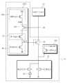
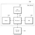
도 9는 본 발명의 실시 예들에 따른 구동 회로가 적용된 불휘발성 메모리 장치의 예를 보여주는 블록도이다. 예시적으로, 도 9에 NAND 플래시 메모리 장치가 도시되어 있다.9 is a block diagram showing an example of a nonvolatile memory device to which a driving circuit according to embodiments of the present invention is applied. Illustratively, a NAND flash memory device is shown in FIG.
도 9를 참조하면, 불휘발성 메모리 장치(110)는 메모리 셀 어레이(111), 행 디코더 회로(113), 페이지 버퍼 회로(115), 데이터 입출력 회로(117), 그리고 제어 로직 회로(119)를 포함한다.9, the
메모리 셀 어레이(111)는 복수의 메모리 블록들(BLK1~BLKz)을 포함한다. 복수의 메모리 블록들(BLK1~BLKz)은 열 방향을 따라 배치될 수 있다. 각 메모리 블록은 행 방향, 열 방향 및 높이 방향을 따라 신장되는 3차원 구조를 가질 수 있다. 각 메모리 블록은 복수의 메모리 셀들을 포함한다. 각 메모리 블록은 적어도 하나의 접지 선택 라인(GSL), 복수의 워드 라인들(WL), 그리고 적어도 하나의 스트링 선택 라인(SSL)을 통해 행 디코더 회로(113)에 연결될 수 있다. 각 메모리 블록은 복수의 비트 라인들(BL)을 통해 페이지 버퍼 회로(115)에 연결될 수 있다. 복수의 비트 라인들(BL)은 열 방향을 따라 신장되며, 복수의 메모리 블록들(BLK1~BLKz)은 복수의 비트 라인들(BL)에 공통으로 연결될 수 있다. 복수의 메모리 블록들(BLK1~BLKz)의 메모리 셀들은 동일한 구조들을 가질 수 있다.The
예시적으로, 복수의 메모리 블록들(BLK1~BLKz) 각각은 소거 동작의 단위일 수 있다. 메모리 셀 어레이(111)의 메모리 셀들은 하나의 메모리 블록의 단위로 소거될 수 있다. 하나의 메모리 블록에 속한 메모리 셀들은 동시에 소거될 수 있다. 다른 예로서, 각 메모리 블록은 복수의 서브 블록들로 분할될 수 있다. 복수의 서브 블록들 각각은 소거 동작의 단위일 수 있다.Illustratively, each of the plurality of memory blocks BLK1 to BLKz may be a unit of an erase operation. The memory cells of the
예시적으로, 복수의 메모리 블록들(BLK1~BLKz) 각각은 블록 어드레스에 의해 식별되는 물리적 저장 공간을 포함할 수 있다. 복수의 워드 라인들(WL) 각각은 행 어드레스에 의해 식별되는 물리적 저장 공간에 대응할 수 있다. 복수의 비트 라인들(BL) 각각은 열 어드레스에 의해 식별되는 물리적 저장 공간에 대응할 수 있다.Illustratively, each of the plurality of memory blocks BLK1 through BLKz may include a physical storage space identified by a block address. Each of the plurality of word lines WL may correspond to a physical storage space identified by a row address. Each of the plurality of bit lines BL may correspond to a physical storage space identified by a column address.
행 디코더 회로(113)는 복수의 접지 선택 라인들(GSL), 복수의 워드 라인들(WL), 그리고 복수의 스트링 선택 라인들(SSL)을 통해 메모리 셀 어레이(111)에 연결된다. 행 디코더 회로(113)는 제어 로직 회로(119)의 제어에 따라 동작한다. 행 디코더 회로(113)는 컨트롤러로부터 입출력 채널을 통해 수신되는 어드레스를 디코딩하고, 디코딩된 어드레스에 따라 스트링 선택 라인들(SSL), 워드 라인들(WL), 그리고 접지 선택 라인들(GSL)에 인가되는 전압들을 제어할 수 있다.The
예를 들어, 프로그램 시에, 행 디코더 회로(113)는, 어드레스에 의해 선택된 메모리 블록의 선택된 워드 라인에 프로그램 전압(VGPM)을 인가하고, 선택된 메모리 블록의 비선택된 워드 라인들에 패스 전압(VPASS)을 인가할 수 있다. 읽기 시에, 행 디코더 회로(113)는 어드레스에 의해 선택된 메모리 블록의 선택된 워드 라인에 선택 읽기 전압(VRD)을 인가하고, 선택된 메모리 블록의 비선택된 워드 라인들에 비선택 읽기 전압(VREAD)을 인가할 수 있다. 소거 시에, 행 디코더 회로(113)는 어드레스에 의해 선택된 메모리 블록의 워드 라인들에 소거 전압들(예를 들어, 접지 전압 또는 접지 전압과 유사한 레벨들을 갖는 저전압들)을 인가할 수 있다.For example, at the time of programming, the
페이지 버퍼 회로(115)는 복수의 비트 라인들(BL)을 통해 메모리 셀 어레이(111)에 연결된다. 페이지 버퍼 회로(115)는 복수의 데이터 라인들(DL)을 통해 데이터 입출력 회로(117)와 연결된다. 페이지 버퍼 회로(115)는 제어 로직 회로(119)의 제어에 따라 동작한다.The
프로그램 시에, 페이지 버퍼 회로(115)는 메모리 셀들에 프로그램될 데이터를 저장할 수 있다. 저장된 데이터에 기반하여, 페이지 버퍼 회로(115)는 복수의 비트 라인들(BL)에 전압들을 인가할 수 있다. 예를 들어, 페이지 버퍼 회로(115)는 쓰기 드라이버로 기능할 수 있다. 읽기 시에, 페이지 버퍼 회로(115)는 비트 라인들(BL)의 전압들을 센싱하고, 센싱 결과를 저장할 수 있다. 예를 들어, 페이지 버퍼 회로(115)는 감지 증폭기로 기능할 수 있다.At the time of programming, the
데이터 입출력 회로(117)는 복수의 데이터 라인들(DL)을 통해 페이지 버퍼 회로(115)와 연결된다. 데이터 입출력 회로(117)는 페이지 버퍼 회로(115)에 의해 읽힌 데이터를 입출력 채널을 통해 컨트롤러로 출력하고, 컨트롤러로부터 입출력 채널을 통해 수신되는 데이터를 페이지 버퍼 회로(115)로 전달할 수 있다.The data input /
제어 로직 회로(119)는 컨트롤러로부터 입출력 채널을 통해 커맨드를 수신하고, 제어 채널을 통해 제어 신호를 수신할 수 있다. 제어 로직 회로(119)는 제어 신호에 응답하여 입출력 채널을 통해 수신되는 커맨드를 수신하고, 입출력 채널을 통해 수신되는 어드레스를 행 디코더 회로(113)로 라우팅하고, 그리고 입출력 채널을 통해 수신되는 데이터를 데이터 입출력 회로(117)로 라우팅할 수 있다. 제어 로직 회로(119)는 수신된 커맨드를 디코딩하고, 디코딩된 커맨드에 따라 불휘발성 메모리 장치(110)를 제어할 수 있다.The
예시적으로, 읽기 시에, 제어 로직 회로(119)는 컨트롤러로부터 제어 채널을 통해 수신되는 읽기 인에이블 신호(/RE)로부터 데이터 스트로브 신호(DQS)를 생성할 수 있다. 생성된 데이터 스트로브 신호(DQS)는 제어 채널을 통해 컨트롤러로 출력될 수 있다. 쓰기 시에, 제어 로직 회로(119)는 컨트롤러로부터 제어 채널을 통해 데이터 스트로브 신호(DQS)를 수신할 수 있다.Illustratively, upon reading, the
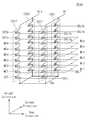
도 10은 본 발명의 실시 예에 따른 메모리 블록(BLKa)을 보여주는 회로도이다. 도 10을 참조하면, 메모리 블록(BLKa)은 복수의 셀 스트링들(CS11~CS21, CS12~CS22)을 포함한다. 복수의 셀 스트링들(CS11~CS21, CS12~CS22)은 행 방향(row direction) 및 열 방향(column direction)을 따라 배열되어, 행들 및 열들을 형성할 수 있다.10 is a circuit diagram showing a memory block BLKa according to an embodiment of the present invention. Referring to FIG. 10, the memory block BLKa includes a plurality of cell strings CS11 to CS21, CS12 to CS22. The plurality of cell strings CS11 to CS21 and CS12 to CS22 may be arranged along a row direction and a column direction to form rows and columns.
예를 들어, 행 방향(row direction)을 따라 배열된 셀 스트링들(CS11, CS12)은 제1 행을 형성하고, 행 방향(row direction)을 따라 배열된 셀 스트링들(CS21, CS22)은 제2 행을 형성할 수 있다. 열 방향(column direction)을 따라 배열된 셀 스트링들(CS11, CS21)은 제1 열을 형성하고, 열 방향(column direction)을 따라 배열된 셀 스트링들(CS12, CS22)은 제2 열을 형성할 수 있다.For example, the cell strings CS11 and CS12 arranged along the row direction form the first row and the cell strings CS21 and CS22 arranged along the row direction form the first row, Two rows can be formed. The cell strings CS11 and CS21 arranged along the column direction form the first column and the cell strings CS12 and CS22 arranged along the column direction form the second column can do.
각 셀 스트링은 복수의 셀 트랜지스터들을 포함할 수 있다. 복수의 셀 트랜지스터들은 접지 선택 트랜지스터들(GST), 메모리 셀들(MC1~MC6), 그리고 스트링 선택 트랜지스터들(SSTa, SSTb)을 포함한다. 각 셀 스트링의 접지 선택 트랜지스터(GST), 메모리 셀들(MC1~MC6), 그리고 스트링 선택 트랜지스터들(SSTa, SSTb)은 셀 스트링들(CS11~CS21, CS12~CS22)이 행들 및 열들을 따라 배열되는 평면(예를 들어, 메모리 블록(BLKa)의 기판 상의 평면)과 수직한 높이 방향으로 적층될 수 있다.Each cell string may include a plurality of cell transistors. The plurality of cell transistors include ground selection transistors GST, memory cells MC1 to MC6, and string selection transistors SSTa and SSTb. The ground selection transistor GST, the memory cells MC1 to MC6 and the string selection transistors SSTa and SSTb of each cell string are arranged such that the cell strings CS11 to CS21 and CS12 to CS22 are arranged along the rows and columns And may be stacked in a height direction perpendicular to the plane (for example, the plane on the substrate of the memory block BLKa).
복수의 셀 트랜지스터들은 절연막에 포획된 전하량에 따라 가변하는 문턱 전압들을 갖는 전하 포획형(charge trap type) 트랜지스터들일 수 있다.The plurality of cell transistors may be charge trap type transistors having threshold voltages varying depending on the amount of charge trapped in the insulating film.
최하단의 접지 선택 트랜지스터들(GST)의 소스들은 공통 소스 라인(CSL)에 공통으로 연결될 수 있다.The sources of the lowermost ground selection transistors (GST) may be connected in common to the common source line (CSL).
제1 행의 셀 스트링들(CS11, CS12)의 접지 선택 트랜지스터들(GST)의 제어 게이트들은 접지 선택 라인(GSL1)에 공통으로 연결되고, 제2 행의 셀 스트링들(CS21, CS22)의 접지 선택 트랜지스터들(GST)의 제어 게이트들은 접지 선택 라인(GSL2)에 공통으로 연결된다. 즉, 서로 다른 행의 셀 스트링들은 서로 다른 접지 선택 라인들에 연결된다.The control gates of the ground selection transistors GST of the cell strings CS11 and CS12 of the first row are commonly connected to the ground selection line GSL1 and the control gates of the cell strings CS21 and CS22 of the second row The control gates of the selection transistors GST are connected in common to the ground selection line GSL2. That is, cell strings in different rows are connected to different ground selection lines.
예시적으로, 동일한 행의 서로 다른 높이의 접지 선택 트랜지스터들이 서로 다른 접지 선택 라인들에 연결되도록 메모리 블록(BLKa)이 변경될 수 있다. 예시적으로, 서로 다른 행의 동일한 높이의 접지 선택 트랜지스터들에 연결되는 접지 선택 트랜지스터들이 서로 연결되어 공통으로 제어되도록 메모리 블록(BLKa)이 변경될 수 있다. 예시적으로, 접지 선택 트랜지스터들에 연결되는 접지 선택 라인들이 서로 연결되어 공통으로 제어되도록 메모리 블록(BLKa)이 변경될 수 있다.Illustratively, the memory block BLKa can be modified such that the ground selection transistors at different heights in the same row are connected to different ground selection lines. Illustratively, the memory block BLKa can be modified such that the ground selection transistors connected to the ground selection transistors at the same height in different rows are coupled together and controlled in common. Illustratively, the memory block BLKa may be modified such that the ground select lines connected to the ground select transistors are coupled together and controlled in common.
기판(또는 접지 선택 트랜지스터들(GST))으로부터 동일한 높이(또는 순서)에 위치한 메모리 셀들의 제어 게이트들은 하나의 워드 라인에 공통으로 연결되고, 서로 다른 높이(또는 순서)에 위치한 메모리 셀들의 제어 게이트들은 서로 다른 워드 라인들(WL1~WL6)에 각각 연결될 수 있다. 예를 들어, 메모리 셀들(MC1)은 워드 라인(WL1)에 공통으로 연결된다. 메모리 셀들(MC2)은 워드 라인(WL2)에 공통으로 연결된다. 메모리 셀들(MC3)은 워드 라인(WL3)에 공통으로 연결된다. 메모리 셀들(MC4)은 워드 라인(WL4)에 공통으로 연결된다. 메모리 셀들(MC5)은 워드 라인(WL5)에 공통으로 연결된다. 메모리 셀들(MC6)은 워드 라인(WL6)에 공통으로 연결된다.The control gates of the memory cells located at the same height (or in sequence) from the substrate (or the ground selection transistors GST) are commonly connected to one word line, and the control gates of the memory cells located at different heights May be connected to different word lines WL1 to WL6, respectively. For example, the memory cells MC1 are commonly connected to the word line WL1. The memory cells MC2 are connected in common to the word line WL2. The memory cells MC3 are commonly connected to the word line WL3. The memory cells MC4 are connected in common to the word line WL4. The memory cells MC5 are commonly connected to the word line WL5. The memory cells MC6 are connected in common to the word line WL6.
복수의 셀 스트링들(CS11~CS21, CS12~CS22)의 동일한 높이(또는 순서)의 제1 스트링 선택 트랜지스터들(SSTa)에서, 서로 다른 행의 제1 스트링 선택 트랜지스터들(SSTa)의 제어 게이트들은 서로 다른 스트링 선택 라인들(SSL1a~SSL2a)에 각각 연결된다. 예를 들어, 셀 스트링들(CS11, CS12)의 제1 스트링 선택 트랜지스터들(SSTa)은 스트링 선택 라인(SSL1a)에 공통으로 연결된다. 셀 스트링들(CS21, CS22)의 제1 스트링 선택 트랜지스터들(SSTa)은 스트링 선택 라인(SSL2a)에 공통으로 연결된다.In the first string selection transistors SSTa of the same height (or order) of the plurality of cell strings CS11 to CS21, CS12 to CS22, the control gates of the first string selection transistors SSTa in different rows And are connected to different string selection lines (SSL1a to SSL2a), respectively. For example, the first string selection transistors SSTa of the cell strings CS11 and CS12 are connected in common to the string selection line SSL1a. The first string selection transistors SSTa of the cell strings CS21 and CS22 are connected in common to the string selection line SSL2a.
복수의 셀 스트링들(CS11~CS21, CS12~CS22)의 동일한 높이(또는 순서)의 제2 스트링 선택 트랜지스터들(SSTb)에서, 서로 다른 행의 제2 스트링 선택 트랜지스터들(SSTb)의 제어 게이트들은 서로 다른 스트링 선택 라인들(SSL1b~SSL2b)에 각각 연결된다. 예를 들어, 셀 스트링들(CS11, CS12)의 제2 스트링 선택 트랜지스터들(SSTb)은 스트링 선택 라인(SSL1b)에 공통으로 연결된다. 셀 스트링들(CS21, CS22)의 제2 스트링 선택 트랜지스터들(SSTb)은 스트링 선택 라인(SSL2b)에 공통으로 연결된다.In the second string selection transistors SSTb of the same height (or order) of the plurality of cell strings CS11 to CS21, CS12 to CS22, the control gates of the second string selection transistors SSTb in different rows And are connected to different string selection lines SSL1b to SSL2b, respectively. For example, the second string selection transistors SSTb of the cell strings CS11 and CS12 are connected in common to the string selection line SSL1b. The second string selection transistors SSTb of the cell strings CS21 and CS22 are connected in common to the string selection line SSL2b.
즉, 서로 다른 행의 셀 스트링들은 서로 다른 스트링 선택 라인들에 연결된다. 동일한 행의 셀 스트링들의 동일한 높이(또는 순서)의 스트링 선택 트랜지스터들은 동일한 스트링 선택 라인에 연결된다. 동일한 행의 셀 스트링들의 서로 다른 높이(또는 순서)의 스트링 선택 트랜지스터들은 서로 다른 스트링 선택 라인들에 연결된다.That is, cell strings in different rows are connected to different string selection lines. The string select transistors of the same height (or sequence) of cell strings in the same row are connected to the same string select line. String selection transistors of different heights (or sequences) of cell strings in the same row are connected to different string selection lines.
예시적으로, 동일한 행의 셀 스트링들의 스트링 선택 트랜지스터들은 하나의 스트링 선택 라인에 공통으로 연결될 수 있다. 예를 들어, 제1 행의 셀 스트링들(CS11, CS12)의 스트링 선택 트랜지스터들(SSTa, SSTb)은 하나의 스트링 선택 라인에 공통으로 연결될 수 있다. 제2 행의 샐 스트링들(CS21, CS22)의 스트링 선택 트랜지스터들(SSTa, SSTb)은 하나의 스트링 선택 라인에 공통으로 연결될 수 있다.By way of example, the string select transistors of the cell strings of the same row may be connected in common to one string select line. For example, the string selection transistors SSTa and SSTb of the cell strings CS11 and CS12 of the first row may be connected in common to one string selection line. The string selection transistors SSTa and SSTb of the sal strings CS21 and CS22 of the second row may be connected in common to one string selection line.
복수의 셀 스트링들(CS11~CS21, CS12~CS22)의 열들은 서로 다른 비트 라인들(BL1, BL2)에 각각 연결된다. 예를 들어, 제1 열의 셀 스트링들(CS11~CS21)의 스트링 선택 트랜지스터들(SSTb)은 비트 라인(BL1)에 공통으로 연결된다. 제2 열의 셀 스트링들(CS12~CS22)의 스트링 선택 트랜지스터들(SST)은 비트 라인(BL2)에 공통으로 연결된다.The columns of the plurality of cell strings CS11 to CS21 and CS12 to CS22 are connected to different bit lines BL1 and BL2, respectively. For example, the string selection transistors SSTb of the cell strings CS11 to CS21 in the first column are connected in common to the bit line BL1. The string selection transistors SST of the cell strings CS12 to CS22 in the second column are connected in common to the bit line BL2.
셀 스트링들(CS11, CS12)은 제1 플레인을 형성할 수 있다. 셀 스트링들(CS21, CS22)은 제2 플레인을 형성할 수 있다.Cell strings CS11 and CS12 may form a first plane. The cell strings CS21 and CS22 may form a second plane.
메모리 블록(BLKa)에서, 각 플레인의 각 높이의 메모리 셀들은 물리 페이지를 형성할 수 있다. 물리 페이지는 메모리 셀들(MC1~MC6)의 쓰기 및 읽기의 단위일 수 있다. 예를 들어, 스트링 선택 라인들(SSL1a, SSL1b, SSL2a, SSL2b)에 의해 메모리 블록(BLKa)의 하나의 플레인이 선택될 수 있다. 스트링 선택 라인들(SSL1a, SSL1b)이 턴-온 전압이 공급되고 스트링 선택 라인들(SSL2a, SSL2b)에 턴-오프 전압이 공급될 때, 제1 플레인의 셀 스트링들(CS11, CS12)이 비트 라인들(BL1, BL2)에 연결된다. 즉, 제1 플레인이 선택된다. 스트링 선택 라인들(SSL2a, SSL2b)에 턴-온 전압이 공급되고 스트링 선택 라인들(SSL1a, SSL1B)에 턴-오프 전압이 공급될 때, 제2 플레인의 셀 스트링들(CS21, CS22)이 비트 라인들(BL1, BL2)에 연결된다. 즉, 제2 플레인이 선택된다. 선택된 플레인에서, 워드 라인들(WL1~WL6)에 의해 메모리 셀들(MC)의 하나의 행이 선택될 수 있다. 선택된 행에서, 제2 워드 라인(WL2)에 선택 전압이 인가되고, 나머지 워드 라인들(WL1, WL3~WL6)에 비선택 전압이 인가될 수 있다. 즉, 스트링 선택 라인들(SSL1a, SSL1b, SSL2a, SSL2b) 및 워드 라인들(WL1~WL6)의 전압들을 조절함으로써, 제2 플레인의 제2 워드 라인(WL2)에 대응하는 물리 페이지가 선택될 수 있다. 선택된 물리 페이지의 메모리 셀들(MC2)에서, 쓰기 또는 읽기가 수행될 수 있다.In the memory block BLKa, memory cells of each height of each plane can form a physical page. The physical page may be a unit of writing and reading of the memory cells MC1 to MC6. For example, one plane of the memory block BLKa may be selected by the string selection lines SSL1a, SSL1b, SSL2a, and SSL2b. When the string selection lines SSL1a and SSL1b are supplied with the turn-on voltage and the turn-off voltage is supplied to the string selection lines SSL2a and SSL2b, the cell strings CS11 and CS12 of the first plane are bit- And connected to lines BL1 and BL2. That is, the first plane is selected. When the turn-on voltage is supplied to the string select lines SSL2a and SSL2b and the turn-off voltage is supplied to the string select lines SSL1a and SSL1B, the cell strings CS21 and CS22 of the second plane are bit- And connected to lines BL1 and BL2. That is, the second plane is selected. In the selected plane, one row of memory cells MC can be selected by the word lines WL1 to WL6. In the selected row, a selection voltage may be applied to the second word line WL2 and a non-selection voltage may be applied to the remaining word lines WL1, WL3 to WL6. That is, by adjusting the voltages of the string selection lines SSL1a, SSL1b, SSL2a, SSL2b and the word lines WL1 to WL6, a physical page corresponding to the second word line WL2 of the second plane can be selected have. In the memory cells MC2 of the selected physical page, writing or reading can be performed.
메모리 셀들(MC) 각각에 둘 이상의 비트들이 기입될 수 있다. 하나의 물리 페이지에 속한 메모리 셀들(MC) 각각에 기입되는 비트들은 논리 페이지들을 형성한다. 하나의 물리 페이지에 속한 메모리 셀들(MC) 각각에 기입되는 첫 번째 비트는 첫 번째 논리 페이지를 형성한다. 하나의 물리 페이지에 속한 메모리 셀들(MC) 각각에 기입되는 N 번째 비트는 N 번째 논리 페이지를 형성한다. 논리 페이지는 데이터 액세스의 단위일 수 있다. 하나의 물리 페이지에서 읽기가 수행될 때에, 논리 페이지의 단위로 데이터가 액세스될 수 있다.More than two bits may be written to each of the memory cells MC. The bits written to each of the memory cells MC belonging to one physical page form logical pages. The first bit written to each of the memory cells MC belonging to one physical page forms the first logical page. The Nth bit written in each of the memory cells MC belonging to one physical page forms an Nth logical page. A logical page may be a unit of data access. When reading is performed in one physical page, data can be accessed in units of logical pages.
메모리 블록(BLKa)에서, 메모리 셀들(MC1~MC6)의 소거는 메모리 블록 단위 또는 서브 블록의 단위로 수행될 수 있다. 메모리 블록 단위로 소거가 수행될 때, 메모리 블록(BLKa)의 모든 메모리 셀들(MC)이 하나의 소거 요청(예를 들어, 외부의 컨트롤러로부터의 소거 요청)에 따라 동시에 소거될 수 있다. 서브 블록의 단위로 수행될 때, 메모리 블록(BLKa)의 메모리 셀들(MC1~MC6) 중 일부는 하나의 소거 요청(예를 들어, 외부의 컨트롤러로부터의 소거 요청)에 따라 동시에 소거되고, 나머지 일부는 소거 금지될 수 있다. 소거되는 메모리 셀들(MC)에 연결된 워드 라인에 저전압(예를 들어, 접지 전압 또는 접지 전압과 유사한 레벨을 갖는 저전압)이 공급되고, 소거 금지된 메모리 셀들(MC)에 연결된 워드 라인은 플로팅될 수 있다.In the memory block BLKa, erasing of the memory cells MC1 to MC6 may be performed in units of memory blocks or units of subblocks. When the erase is performed on a memory block basis, all the memory cells MC of the memory block BLKa can be erased simultaneously according to one erase request (for example, an erase request from an external controller). Some of the memory cells MC1 to MC6 of the memory block BLKa are simultaneously erased in response to one erase request (for example, an erase request from the external controller), and the remaining part Lt; / RTI > A word line connected to the erased memory cells MC is supplied with a low voltage (e.g., a ground voltage or a low voltage having a level similar to the ground voltage), and the word line connected to the erased memory cells MC can be floated have.
도 10에 도시된 메모리 블록(BLKa)은 예시적인 것이다. 본 발명의 기술적 사상은 도 10에 도시된 메모리 블록(BLKa)에 한정되지 않는다. 예를 들어, 셀 스트링들의 행들의 수는 증가 또는 감소될 수 있다. 셀 스트링들의 행들의 수가 변경됨에 따라, 셀 스트링들의 행들에 연결되는 스트링 선택 라인들 또는 접지 선택 라인의 수, 그리고 하나의 비트 라인에 연결되는 셀 스트링들의 수 또한 변경될 수 있다.The memory block BLKa shown in Fig. 10 is an exemplary one. The technical idea of the present invention is not limited to the memory block BLKa shown in Fig. For example, the number of rows of cell strings may be increased or decreased. As the number of rows of cell strings is changed, the number of string select lines or ground select lines connected to the rows of cell strings, and the number of cell strings connected to one bit line can also be changed.
셀 스트링들의 열들의 수는 증가 또는 감소될 수 있다. 셀 스트링들의 열들의 수가 변경됨에 따라, 셀 스트링들의 열들에 연결되는 비트 라인들의 수, 그리고 하나의 스트링 선택 라인에 연결되는 셀 스트링들의 수 또한 변경될 수 있다.The number of columns of cell strings can be increased or decreased. As the number of columns of cell strings changes, the number of bit lines connected to columns of cell strings and the number of cell strings connected to one string selection line can also be changed.
셀 스트링들의 높이는 증가 또는 감소될 수 있다. 예를 들어, 셀 스트링들 각각에 적층되는 접지 선택 트랜지스터들, 메모리 셀들 또는 스트링 선택 트랜지스터들의 수는 증가 또는 감소될 수 있다.The height of the cell strings can be increased or decreased. For example, the number of ground select transistors, memory cells, or string select transistors stacked on each of the cell strings may be increased or decreased.
예시적으로, 하나의 물리 페이지에 속한 메모리 셀들(MC)은 적어도 세 개의 논리 페이지들에 대응할 수 있다. 예를 들어, 하나의 메모리 셀(MC)에 k 개(k는 2보다 큰 양의 정수)의 비트들이 프로그램될 수 있다. 하나의 물리 페이지에 속한 메모리 셀들(MC)에서, 각 메모리 셀(MC)에 프로그램되는 k 개의 비트들은 각각 k 개의 논리 페이지들을 형성할 수 있다.Illustratively, memory cells MC belonging to one physical page may correspond to at least three logical pages. For example, k (k is a positive integer greater than 2) bits can be programmed into one memory cell MC. In the memory cells MC belonging to one physical page, the k bits programmed into each memory cell MC can form k logical pages, respectively.
상술된 바와 같이, 메모리 블록(BLKa)은 3차원 메모리 어레이로 제공된다. 3차원 메모리 어레이는, 실리콘 기판 및 메모리 셀들(MC)의 동작에 연관된 회로의 위에 배치되는 활성 영역을 갖는 메모리 셀들(MC)의 어레이들의 하나 또는 그 이상의 물리 레벨들에 획일적으로(monolithically) 형성될 수 있다. 메모리 셀들(MC)의 동작에 연관된 회로는 기판 내에 또는 기판 위에 위치할 수 있다. 획일적으로 형성되는 것은, 3차원 어레이의 각 레벨의 레이어들이 3차원 어레이의 하위 레벨의 레이어들 위에 직접 증착됨을 의미한다.As described above, the memory block BLKa is provided as a three-dimensional memory array. The three dimensional memory array may be formed monolithically on one or more physical levels of arrays of memory cells MC having active regions disposed above the circuitry associated with the operation of the silicon substrate and memory cells MC . The circuitry associated with the operation of the memory cells MC may be located within or on the substrate. What is uniformly formed means that the layers of each level of the three-dimensional array are directly deposited on the lower-level layers of the three-dimensional array.
본 발명의 기술적 사상에 따른 일 예로서, 3차원 메모리 어레이는 수직의 방향성을 가져, 적어도 하나의 메모리 셀이 다른 하나의 메모리 셀 위에 위치하는 수직 NAND 스트링들(또는 셀 스트링들)을 포함한다. 적어도 하나의 메모리 셀(MC)은 전하 포획 레이어를 포함한다. 각 수직 NAND 스트링은 메모리 셀들(MC) 위에 위치하는 적어도 하나의 선택 트랜지스터를 더 포함한다. 적어도 하나의 선택 트랜지스터는 메모리 셀들(MC)과 동일한 구조를 갖고, 메모리 셀들(MC)과 함께 획일적으로 형성된다.As an example according to the technical idea of the present invention, a three-dimensional memory array includes vertical NAND strings (or cell strings) having vertical directionality, and at least one memory cell is located on another memory cell. At least one memory cell (MC) includes a charge trapping layer. Each vertical NAND string further includes at least one select transistor located above the memory cells MC. At least one selection transistor has the same structure as the memory cells MC and is uniformly formed with the memory cells MC.
3차원 메모리 어레이가 복수의 레벨들로 구성되고, 레벨들 사이에서 워드 라인들 또는 비트 라인들이 공유되는 구성은 미국등록특허공보 제7,679,133호, 미국등록특허공보 제8,553,466호, 미국등록특허공보 제8,654,587호, 미국등록특허공보 제8,559,235호, 그리고 미국공개특허공보 제2011/0233648호에 개시되어 있으며, 본 발명의 레퍼런스로 포함된다.A configuration in which the three-dimensional memory array is composed of a plurality of levels and the word lines or bit lines are shared between levels is disclosed in U.S. Patent No. 7,679,133, U.S. Patent No. 8,553,466, U.S. Patent No. 8,654,587 U.S. Patent No. 8,559,235, and U.S. Published Patent Application No. 2011/0233648, which are incorporated herein by reference.
상술된 바와 같이, 메모리 블록들(BLK1~BLKz)은 비트 라인들(BL)을 공유한다. 각 비트 라인은 각 메모리 블록에서 복수의 셀 스트링들과 연결된다. 따라서, 각 비트 라인의 저항 부하 및 용량 부하로 인해, 각 비트 라인을 목표 전압으로 구동하는 것은 긴 시간을 필요로 한다. 각 비트 라인을 목표 전압으로 구동하는데에 필요한 시간을 감소시키기 위하여, 본 발명의 실시 예들에 따른 구동 회로(13, 14, 15 또는 16)가 사용될 수 있다. 마찬가지로, 각 워드 라인을 목표 전압으로 구동하는데에 필요한 시간을 감소시키기 위하여, 본 발명의 실시 예들에 따른 구동 회로(13, 14, 15 또는 16)가 사용될 수 있다.As described above, the memory blocks BLK1 to BLKz share the bit lines BL. Each bit line is connected to a plurality of cell strings in each memory block. Therefore, due to the resistive load and the capacitive load of each bit line, driving each bit line to the target voltage requires a long time. In order to reduce the time required to drive each bit line to the target voltage, the driving
도 11은 본 발명의 실시 예들에 따른 구동 회로(13, 14, 15 또는 16)가 적용되는 페이지 버퍼 회로(115)의 일부(115_1)를 보여주는 블록도이다. 예시적으로, 하나의 비트 라인(BL)에 대응하는 페이지 버퍼 회로(115)의 일부 구성(115_1)이 도 11에 도시되어 있다. 도 11을 참조하면, 페이지 버퍼 회로(115_1)는 비트 라인(BL)에 연결되는 프리차지 회로(PC) 및 페이지 버퍼(PB)를 포함한다.11 is a block diagram showing a portion 115_1 of the
페이지 버퍼(PB)는 센스 래치(SL), 제1 덤프 회로(DC1), 제1 내지 제k 데이터 래치들(DL1~DLk), 제2 덤프 회로(DC2), 그리고 캐시 래치(CL)를 포함한다.The page buffer PB includes a sense latch SL, a first dump circuit DC1, first to kth data latches DL1 to DLk, a second dump circuit DC2, and a cache latch CL do.
센스 래치(SL)는 저장된 비트에 따라 비트 라인(BL)에 전압(예를 들어, 세팅 전압(VSET))을 인가하는 바이어스 동작, 또는 비트 라인(BL)의 전압에 따라 비트를 저장하는 센싱 동작을 수행할 수 있다. 센스 래치(SL)는 제1 덤프 회로(DC1)를 통해 전달되는 비트를 저장하거나, 또는 저장된 비트를 제1 덤프 회로(DC1)로 전달할 수 있다.The sense latch SL includes a bias operation for applying a voltage (for example, a setting voltage VSET) to the bit line BL in accordance with a stored bit or a sensing operation for storing a bit according to the voltage of the bit line BL Can be performed. The sense latch SL may store the bit transmitted through the first dump circuit DC1 or may transmit the stored bit to the first dump circuit DC1.
제1 덤프 회로(DC1)는 제1 내지 제k 데이터 래치들(DL1~DLk)에 저장된 비트들에 기반하여 센스 래치(DC1)에 비트를 저장하거나 또는 센스 래치(SL)에 저장된 비트를 제1 내지 제k 데이터 래치들(DL1~DLk) 중 하나로 전달하는 덤핑 동작을 수행할 수 있다.The first dump circuit DC1 stores bits in the sense latch DC1 or bits stored in the sense latch SL based on the bits stored in the first to k-th data latches DL1 to DLk, To one of the k-th data latches DL1-DLk.
제1 내지 제k 데이터 래치들(DL1~DLk)은 센스 래치(SL)로부터 제1 덤핑 회로(DC1)를 통해 전달되는 비트들, 즉 비트 라인(BL)에 연결된 메모리 셀로부터 읽힌 비트들을 저장할 수 있다. 또한, 제1 내지 제k 데이터 래치들(DL1~DLk)은 제1 덤핑 회로(DC1)를 통해 센스 래치(SL)로 전달될 비트들, 즉 비트 라인(BL)에 연결된 메모리 셀에 기입될 비트들을 저장할 수 있다. 제1 내지 제k 데이터 래치들(DL1~DLk) 중 선택된 데이터 래치는 저장된 비트를 제2 덤핑 회로(DC2)로 전달할 수 있다. 제1 내지 제k 데이터 래치들(DL1~DLk) 중 선택된 데이터 래치는 제2 덤핑 회로(DC2)로부터 전달된 비트를 저장할 수 있다. 제1 내지 제k 데이터 래치들(DL1~DLk)의 수는 비트 라인(BL)에 연결된 메모리 셀에 기입되는 비트들의 수와 같거나 그보다 많을 수 있다.The first to kth data latches DL1 to DLk are capable of storing bits read from the memory cell connected to the bits transmitted from the sense latch SL via the first dumping circuit DC1, have. The first to k-th data latches DL1 to DLk are connected to the bits to be transferred to the sense latch SL via the first dumping circuit DC1, that is, bits to be written to the memory cells connected to the bit line BL Lt; / RTI > The selected one of the first through k-th data latches DL1-DLk may carry the stored bit to the second dumping circuit DC2. The selected one of the first to k-th data latches DL1 to DLk may store the bit transmitted from the second dumping circuit DC2. The number of the first to k-th data latches DL1 to DLk may be equal to or greater than the number of bits written to the memory cell connected to the bit line BL.
제2 덤핑 회로(DC2)는 제1 내지 제k 데이터 래치들(DL1~DLk) 중 선택된 데이터 래치에 저장된 데이터를 캐시 래치(CL)로 전달할 수 있다. 제2 덤핑 회로(DC2)는 캐시 래치(CL)에 저장된 비트를 제1 내지 제k 데이터 래치들(DL1~DLk) 중 선택된 데이터 래치로 전달할 수 있다.The second dumping circuit DC2 may transfer the data stored in the selected one of the first to k-th data latches DL1 to DLk to the cache latch CL. The second dumping circuit DC2 may transfer the bits stored in the cache latch CL to the selected one of the first to k-th data latches DL1 to DLk.
프리차지 회로(PC)는 도 5 내지 도 8을 참조하여 설명된 구동 회로들(13~16) 중 하나 또는 그 이상을 포함할 수 있다. 예를 들어, 프리차지 회로(PC)는 비트 라인(BL)을 미리 정해진 세팅 전압(VSET)(예를 들어, 전원 전압)으로 충전하도록 구성될 수 있다. 이 때, 프리차지 회로(PC)는 하나 또는 그 이상의 구동 회로들을 이용하여, 비트 라인(BL)이 세팅 전압(VSET) 또는 세팅 전압(VSET)과 유사한 레벨을 추종하도록 제어할 수 있다. 센스 래치(SL)에 의해 비트 라인(BL)이 세팅 전압(VSET)(예를 들어, 전원 전압 또는 접지 전압)으로 바이어스될 때, 비트 라인(BL)의 전압이 세팅 전압(VSET) 또는 그와 유사한 레벨을 추종하도록 제어할 수 있다.The precharge circuit PC may include one or more of the
예시적으로, 센스 래치(SL)는 도 5 내지 도 8을 참조하여 설명된 구동 회로들(13~16) 중 하나 또는 그 이상을 포함할 수 있다. 예를 들어, 센스 래치(SL)는 저장된 비트에 따라 비트 라인(BL)에 접지 전압 또는 전원 전압을 바이어스하도록 구성된다. 센스 래치(SL)는 하나 또는 그 이상의 구동 회로들을 이용하여 바이어스 동작을 수행할 수 있다.Illustratively, the sense latch SL may include one or more of the drive circuits 13-16 as described with reference to Figs. 5-8. For example, the sense latch SL is configured to bias the ground voltage or the supply voltage to the bit line BL according to the stored bit. The sense latch SL may perform a bias operation using one or more driving circuits.
도 12는 본 발명의 실시 예들에 따른 구동 회로(13, 14, 15 또는 16)가 적용되는 행 디코더 회로(113)의 일부(113_1)를 보여주는 블록도이다. 예시적으로, 하나의 메모리 블록에 대응하는 행 디코더 회로(113)의 일부 구성(113_1)이 도 12에 도시되어 있다. 도 12을 참조하면, 행 디코더 회로(113_1)는 메모리 블록의 워드 라인들(WL1~WLn)에 연결되는 패스 트랜지스터들(PTR), 블록 디코더(BDEC), 그리고 워드 라인 드라이버(WLD)를 포함한다.12 is a block diagram showing a part 113_1 of the
워드 라인 드라이버(WLD)는 복수의 내부 라인들(SI)을 구동하도록 구성된다. 예시적으로, 워드 라인 드라이버(WLD)가 구동하는 내부 라인들(SI)의 수는 하나의 메모리 블록에 속한 워드 라인들과 동일할 수 있다. 각 내부 라인은 각 메모리 블록의 각 워드 라인에 대응할 수 있다.The word line driver (WLD) is configured to drive a plurality of internal lines (SI). Illustratively, the number of internal lines (SI) driven by the word line driver (WLD) may be the same as the word lines belonging to one memory block. Each internal line may correspond to each word line of each memory block.
블록 디코더(BDEC)는 행 디코더 회로(113)에 전달되는 블록 어드레스에 기반하여, 복수의 메모리 블록들(BLK1~BLKz, 도 9 참조) 중 하나의 메모리 블록을 선택할 수 있다. 블록 디코더(BDEC)는 선택된 메모리 블록에 대응하는 패스 트랜지스터들(PTR)을 턴-온 할 수 있다. 즉, 블록 디코더(BDEC)는 선택된 메모리 블록의 워드 라인들(WL1~WLn)을 내부 라인들(SI)과 전기적으로 연결할 수 있다.The block decoder BDEC can select one of the plurality of memory blocks BLK1 to BLKz (see FIG. 9), based on the block address transmitted to the
워드 라인 드라이버(WLD)는 도 5 내지 도 8을 참조하여 설명된 구동 회로들(13~16) 중 하나 또는 그 이상을 포함할 수 있다. 워드 라인 드라이버(WLD)는 하나 또는 그 이상의 구동 회로들을 이용하여, 내부 라인들(SI) 및 워드 라인들(WL1~WLn)의 전압들을 구동할 수 있다.The word line driver (WLD) may include one or more of the driving
마찬가지로, 스트링 선택 라인들(SSL)을 구동하는 스트링 선택 라인 드라이버 및 접지 선택 라인들(GSL)을 구동하는 접지 선택 라인 드라이버가 행 디코더 회로(113)에 포함될 수 있다. 스트링 선택 라인 드라이버 및 접지 선택 라인 드라이버는 하나 또는 그 이상의 구동 회로들을 이용하여 스트링 선택 라인들(SSL) 및 접지 선택 라인들(GSL)을 각각 구동하도록 구성될 수 있다.Similarly, the string selection line driver driving the string selection lines SSL and the ground selection line driver driving the ground selection lines GSL may be included in the
도 13은 본 발명의 실시 예들에 따른 구동 회로가 적용된 불휘발성 메모리 장치의 다른 예를 보여주는 블록도이다. 예시적으로, 도 13에 크로스-포인트 타입의 메모리 장치가 도시되어 있다. 크로스-포인트 타입의 메모리 장치는 워드 라인과 비트 라인의 교차점(크로스-포인트)에, 워드 라인 및 비트 라인과 연결되는 메모리 셀이 배치되는 구조를 갖는다. 예시적으로, RRAM (Resistive Random Access Memory), PRAM (Phase-change RAM), FeRAM (Ferroelectric RAM), MRAM (Magnetic RAM)과 같이, 불휘발성 RAM들이 크로스-포인트 타입으로 구현될 수 있다.13 is a block diagram showing another example of a nonvolatile memory device to which the driving circuit according to the embodiments of the present invention is applied. Illustratively, a cross-point type memory device is shown in Fig. A cross-point type memory device has a structure in which memory cells connected to word lines and bit lines are disposed at the intersections (cross-points) of word lines and bit lines. Illustratively, nonvolatile RAMs, such as Resistive Random Access Memory (RRAM), Phase-change RAM (PRAM), Ferroelectric RAM (FeRAM), and Magnetic RAM (MRAM), may be implemented as a cross-point type.
도 13을 참조하면, 불휘발성 메모리 장치(210)는 메모리 셀 어레이(211), 행 디코더 회로(213), 감지 증폭기 및 쓰기 드라이버 회로(215), 데이터 입출력 회로(217), 그리고 제어 로직 회로(219)를 포함한다.13, the
메모리 셀 어레이(111)는 복수의 메모리 타일들(TILE1~TILEz)을 포함한다. 복수의 메모리 타일들(TILE1~TILEz)은 높이 방향을 따라 적층될 수 있다. 각 메모리 타일은 행 방향, 열 방향 및 높이 방향을 따라 신장되는 3차원 구조를 가질 수 있다. 복수의 메모리 타일들(TILE1~TILEz)은 복수의 글로벌 워드 라인들(GWL)을 통해 행 디코더 회로(113)에 공통으로 연결될 수 있다. 복수의 메모리 타일들(TILE1~TILEz)은 복수의 글로벌 비트 라인들(GBL)을 통해 감지 증폭기 및 쓰기 드라이버 회로(215)에 공통으로 연결될 수 있다.The
각 메모리 타일은 복수의 메모리 셀들을 포함한다. 각 메모리 타일의 복수의 메모리 셀들은 복수의 글로벌 워드 라인들(GWL)과 연결되는 복수의 워드 라인들에 연결될 수 있다. 각 메모리 타일에 속한 워드 라인들은 다른 타일들로부터 독립적일 수 있다. 각 메모리 타일의 메모리 셀들은 복수의 글로벌 비트 라인들(GBL)에 연결되는 복수의 비트 라인들에 연결될 수 있다. 각 메모리 타일에 속한 비트 라인들은 다른 타일들로부터 독립적일 수 있다.Each memory tile includes a plurality of memory cells. A plurality of memory cells of each memory tile may be connected to a plurality of word lines connected to a plurality of global word lines (GWL). The word lines belonging to each memory tile may be independent of other tiles. The memory cells of each memory tile may be connected to a plurality of bit lines connected to a plurality of global bit lines GBL. The bit lines belonging to each memory tile may be independent of other tiles.
행 디코더 회로(213)는 복수의 글로벌 워드 라인들(GWL)을 통해 메모리 셀 어레이(211)에 연결된다. 행 디코더 회로(213)는 제어 로직 회로(219)의 제어에 따라 동작한다. 행 디코더 회로(213)는 컨트롤러로부터 입출력 채널을 통해 수신되는 어드레스를 디코딩하고, 디코딩된 어드레스에 따라 글로벌 워드 라인들(GWL)에 인가되는 전압들을 제어할 수 있다.The
감지 증폭기 및 쓰기 드라이버 회로(215)는 복수의 글로벌 비트 라인들(GBL)을 통해 메모리 셀 어레이(211)에 연결된다. 감지 증폭기 및 쓰기 드라이버 회로는 복수의 데이터 라인들(DL)을 통해 데이터 입출력 회로(217)와 연결된다. 감지 증폭기 및 쓰기 드라이버 회로(215)는 제어 로직 회로(219)의 제어에 따라 동작한다.The sense amplifier and write
데이터 입출력 회로(217)는 복수의 데이터 라인들(DL)을 통해 감지 증폭기 및 쓰기 드라이버 회로(215)와 연결된다. 데이터 입출력 회로(217)는 감지 증폭기 및 쓰기 드라이버 회로(215)에 의해 읽힌 데이터를 입출력 채널을 통해 컨트롤러로 출력하고, 컨트롤러로부터 입출력 채널을 통해 수신되는 데이터를 감지 증폭기 및 쓰기 드라이버 회로(215)로 전달할 수 있다.The data input /
제어 로직 회로(219)는 컨트롤러로부터 입출력 채널을 통해 커맨드를 수신하고, 제어 채널을 통해 제어 신호를 수신할 수 있다. 제어 로직 회로(219)는 제어 신호에 응답하여 입출력 채널을 통해 수신되는 커맨드를 수신하고, 입출력 채널을 통해 수신되는 어드레스를 행 디코더 회로(213)로 라우팅하고, 그리고 입출력 채널을 통해 수신되는 데이터를 데이터 입출력 회로(217)로 라우팅할 수 있다. 제어 로직 회로(219)는 수신된 커맨드를 디코딩하고, 디코딩된 커맨드에 따라 불휘발성 메모리 장치(210)를 제어할 수 있다.The
도 14는 본 발명의 실시 예에 따른 메모리 타일(TILEk)을 보여주는 회로도이다. 도 14를 참조하면, 메모리 타일(TILEk)에서, 비트 라인들 및 워드 라인들이 높이 방향을 따라 순차적으로 적층된다. 예를 들어, 도 14에서, 비트 라인들(BL1_1, BL1_2)이 제1 평면에 배치될 수 있다. 비트 라인들(BL1_1, BL1_2)은 열 방향을 따라 신장되며, 행 방향을 따라 서로 이격될 수 있다.14 is a circuit diagram showing a memory tile TILEk according to an embodiment of the present invention. Referring to FIG. 14, in the memory tile TILEk, the bit lines and the word lines are sequentially stacked along the height direction. For example, in FIG. 14, the bit lines BL1_1 and BL1_2 may be arranged in the first plane. The bit lines BL1_1 and BL1_2 extend along the column direction and can be spaced apart from each other along the row direction.
제1 평면 상의 제2 평면에서, 워드 라인들(WL1_1, WL1_2)이 배치될 수 있다. 워드 라인들(WL1_1, WL1_2)은 행 방향을 따라 신장되며, 열 방향을 따라 서로 이격될 수 있다.In the second plane on the first plane, the word lines WL1_1, WL1_2 can be arranged. The word lines WL1_1 and WL1_2 extend along the row direction and can be spaced from each other along the column direction.
제1 평면과 제2 평면의 사이에서, 비트 라인들(BL1_1, BL1_2) 및 워드 라인들(WL1_1, WL1_2)의 크로스-포인트에 메모리 셀들(MC)이 배치될 수 있다. 각 메모리 셀은 하나의 워드 라인 및 하나의 비트 라인에 연결될 수 있다.Between the first plane and the second plane, the memory cells MC can be arranged at the cross-points of the bit lines BL1_1, BL1_2 and the word lines WL1_1, WL1_2. Each memory cell may be connected to one word line and one bit line.
제2 평면 상의 제3 평면에서, 비트 라인들(BL2_1, BL2_2)이 배치될 수 있다. 비트 라인들(BL2_1, BL2_2)은 열 방향을 따라 신장되며, 행 방향을 따라 서로 이격될 수 있다.In the third plane on the second plane, bit lines BL2_1 and BL2_2 may be arranged. The bit lines BL2_1 and BL2_2 extend along the column direction and can be spaced from each other along the row direction.
제2 평면과 제3 평면의 사이에서, 비트 라인들(BL2_1, BL2_2) 및 워드 라인들(WL1_1, WL1_2)의 크로스-포인트에 메모리 셀들(MC)이 배치될 수 있다. 각 메모리 셀은 하나의 워드 라인 및 하나의 비트 라인에 연결될 수 있다.Between the second plane and the third plane, the memory cells MC can be arranged at the cross-points of the bit lines BL2_1, BL2_2 and the word lines WL1_1, WL1_2. Each memory cell may be connected to one word line and one bit line.
제3 평면 상의 제4 평면에서, 워드 라인들(WL2_1, WL2_2)이 배치될 수 있다. 워드 라인들(WL2_1, WL2_2)은 행 방향을 따라 신장되며, 열 방향을 따라 서로 이격될 수 있다.In the fourth plane on the third plane, the word lines WL2_1 and WL2_2 can be arranged. The word lines WL2_1 and WL2_2 extend along the row direction and can be spaced from each other along the column direction.
제3 평면과 제4 평면의 사이에서, 비트 라인들(BL2_1, BL2_2) 및 워드 라인들(WL2_1, WL2_2)의 크로스-포인트에 메모리 셀들(MC)이 배치될 수 있다. 각 메모리 셀은 하나의 워드 라인 및 하나의 비트 라인에 연결될 수 있다.Between the third and fourth planes, the memory cells MC can be arranged at the cross-points of the bit lines BL2_1, BL2_2 and the word lines WL2_1, WL2_2. Each memory cell may be connected to one word line and one bit line.
각 메모리 셀은 가변 저항 소자(VR) 및 선택 소자(S)를 포함할 수 있다. 가변 저항 소자(VR)의 저항값은 워드 라인과 비트 라인의 전압들이 제1 조건에 속할 때에 증가(예를 들어, 셋 또는 쓰기)될 수 있다. 가변 저항 소자(VR)의 저항값은 워드 라인과 비트 라인의 전압들이 제2 조건에 속할 때에 감소(예를 들어, 리셋 또는 소거)될 수 있다. 워드 라인과 비트 라인의 전압들이 제1 조건 및 제2 조건에 속하지 않을 때에, 가변 저항 소자(VR)의 저항값은 유지될 수 있다.Each memory cell may include a variable resistance element (VR) and a selection element (S). The resistance value of the variable resistive element VR may be increased (e.g., set or written) when the voltages of the word line and the bit line belong to the first condition. The resistance value of the variable resistive element VR may be reduced (e.g., reset or erased) when the voltages of the word line and the bit line belong to the second condition. When the voltages of the word line and the bit line do not belong to the first condition and the second condition, the resistance value of the variable resistive element VR can be maintained.
선택 소자(S)는 다이오드를 포함할 수 있다. 선택 소자(S)는 해당 메모리 셀의 선택성을 제공할 수 있다. 예를 들어, 선택 소자(S)는 워드 라인과 비트 라인의 전압들에 따라 전류를 통과시킴으로써, 해당 메모리 셀이 선택되도록 할 수 있다. 선택 소자(S)는 워드 라인과 비트 라인의 전압들에 따라 전류를 차단함으로써, 해당 메모리 셀이 비선택되도록 할 수 있다. 예시적으로, 선택 소자(S)는 트랜지스터로 대체될 수 있다. 예시적으로, 각 메모리 셀(MC)을 선택하기 위해 선택 소자(S)를 사용하는 대신에, 워드 라인 및 비트 라인의 전압을 제어하는 방법이 사용될 수 있다. 예를 들어, 비선택된 메모리 셀에 연결된 워드 라인과 비트 라인의 전압들을 동일하게 제어함으로써, 비선택된 메모리 셀에 전류가 흐르지 않을 수 있다. 선택된 메모리 셀에 연결된 워드 라인과 비트 라인의 전압들을 서로 다르게 제어함으로써, 선택된 메모리 셀에 전류가 흐를 수 있다. 선택 소자(S) 대신에 전압들을 조절하는 방법이 사용되는 경우, 각 메모리 셀에 선택 소자(S)가 제공되지 않을 수 있다.The selection element S may comprise a diode. The selection element S can provide the selectivity of the memory cell. For example, the selection element S may cause the selected memory cell to be selected by passing a current in accordance with the voltages of the word line and the bit line. The selection element S may cause the memory cell to be unselected by interrupting the current in accordance with the voltages of the word line and the bit line. Illustratively, the selection element S may be replaced by a transistor. Illustratively, instead of using the selection element S to select each memory cell MC, a method of controlling the voltage of the word line and the bit line may be used. For example, by controlling the voltages of the word lines and bit lines connected to the unselected memory cells equally, current may not flow through the unselected memory cells. By controlling the voltages of the word line and bit line connected to the selected memory cell differently, current can flow in the selected memory cell. If a method of adjusting voltages instead of the selection element S is used, the selection element S may not be provided in each memory cell.
가변 저항 소자(VR)는 저항성(Resistive) 타입, 상 변화(Phase-change) 타입, 자기(Magnetic) 타입, 또는 강유전(Ferroelectric) 타입일 수 있다.The variable resistive element VR may be a resistive type, a phase-change type, a magnetic type, or a ferroelectric type.
상술된 바와 같이, 메모리 타일들(TILE1~TILEz)은 글로벌 비트 라인들(GBL)을 공유한다. 각 글로벌 비트 라인은 각 메모리 타일에서 복수의 비트 라인들과 연결된다. 따라서, 각 글로벌 비트 라인의 저항 부하 및 용량 부하로 인해, 각 글로벌 비트 라인을 목표 전압으로 구동하는 것은 긴 시간을 필요로 한다. 각 글로벌 비트 라인을 목표 전압으로 구동하는데에 필요한 시간을 감소시키기 위하여, 본 발명의 실시 예들에 따른 구동 회로(13, 14, 15 또는 16)가 사용될 수 있다. 마찬가지로, 각 글로벌 워드 라인을 목표 전압으로 구동하는데에 필요한 시간을 감소시키기 위하여, 본 발명의 실시 예들에 따른 구동 회로(13, 14, 15 또는 16)가 사용될 수 있다.As described above, the memory tiles TILE1 to TILEz share global bit lines GBL. Each global bit line is connected to a plurality of bit lines in each memory tile. Therefore, due to the resistance load and the capacity load of each global bit line, driving each global bit line to the target voltage requires a long time. In order to reduce the time required to drive each global bit line to a target voltage, a
도 15는 본 발명의 실시 예들에 따른 구동 회로(13, 14, 15 또는 16)가 사용되는 행 디코더 회로(213)의 일부(213_1) 및 감지 증폭기 및 쓰기 드라이버 회로(215)의 일부(215_1)를 보여주는 블록도이다.15 shows a portion 213_1 of the
도 15를 참조하면, 행 디코더 회로(213)는 각 글로벌 워드 라인(GWL)에 대응하는 글로벌 워드 라인 드라이버를 포함할 수 있다. 글로벌 워드 라인 드라이버는 도 5 내지 도 8을 참조하여 설명된 구동 회로들(13~16) 중 하나 또는 그 이상을 이용하여 글로벌 워드 라인(GWL)을 구동하도록 구성될 수 있다.Referring to FIG. 15, the
감지 증폭기 및 쓰기 드라이버 회로(215)는 각 글로벌 비트 라인을 구동하는 글로벌 비트 라인 드라이버를 포함할 수 있다. 글로벌 비트 라인 드라이버는 도 5 내지 도 8을 참조하여 설명된 구동 회로들(13~16) 중 하나 또는 그 이상을 이용하여 글로벌 비트 라인(GBL)을 구동하도록 구성될 수 있다.The sense amplifier and write
도 16은 본 발명의 실시 예에 따른 스토리지 장치(100)를 보여주는 블록도이다. 도 16을 참조하면, 스토리지 장치(100)는 불휘발성 메모리 장치(110), 컨트롤러(120), 그리고 RAM (130)을 포함한다.16 is a block diagram showing a
불휘발성 메모리 장치(110)는 컨트롤러(120)의 제어에 따라 쓰기, 읽기 및 소거를 수행할 수 있다. 불휘발성 메모리 장치(110)는 입출력 채널을 통해 컨트롤러(120)로부터 커맨드 및 어드레스를 수신할 수 있다. 불휘발성 메모리 장치(110)는 입출력 채널을 통해 컨트롤러(120)와 데이터를 교환할 수 있다.The
불휘발성 메모리 장치(110)는 플래시 메모리를 포함할 수 있다. 그러나, 불휘발성 메모리 장치(110)는 플래시 메모리를 포함하는 것으로 한정되지 않는다. 불휘발성 메모리 장치(110)는 PRAM (Phase-change RAM), MRAM (Magnetic RAM), RRAM (Resistive RAM), FeRAM (Ferroelectric RAM) 등과 같은 다양한 불휘발성 메모리 장치들 중 적어도 하나를 포함할 수 있다.The
컨트롤러(120)는 불휘발성 메모리 장치(110)를 제어하도록 구성된다. 예를 들어, 컨트롤러(120)는 불휘발성 메모리 장치(110)가 쓰기, 읽기 또는 소거를 수행하도록 입출력 채널 및 제어 채널을 통해 불휘발성 메모리 장치(110)를 제어할 수 있다.The
컨트롤러(120)는 외부의 호스트 장치(미도시)의 제어에 따라 불휘발성 메모리 장치(110)를 제어할 수 있다. 예를 들어, 컨트롤러(120)는 불휘발성 메모리 장치(110)와 통신하는 포맷과 다른 포맷에 따라 외부의 호스트 장치와 통신할 수 있다. 컨트롤러(120)가 불휘발성 메모리 장치(110)와 통신하는 데이터의 단위는 외부의 호스트 장치와 통신하는 데이터의 단위와 다를 수 있다.The
컨트롤러(120)는 RAM (130)을 버퍼 메모리, 캐시 메모리, 또는 동작 메모리로 사용할 수 있다. 컨트롤러(120)는 불휘발성 메모리 장치(110)를 관리하기 위해 필요한 데이터 또는 코드를 RAM (130)에 저장할 수 있다. 예를 들어, 컨트롤러(120)는 불휘발성 메모리 장치(110)를 관리하기 위해 필요한 데이터 또는 코드를 불휘발성 메모리 장치(110)로부터 읽고, RAM (130)에 로딩하여 구동할 수 있다.The
RAM (130)은 DRAM (Dynamic RAM), SRAM (Static RAM), SDRAM (Synchronous DRAM), PRAM (Phase-change RAM), MRAM (Magnetic RAM), RRAM (Resistive RAM), FeRAM (Ferroelectric RAM) 등과 같은 다양한 랜덤 액세스 메모리 장치들 중 적어도 하나를 포함할 수 있다.The
스토리지 장치(100)는 솔리드 스테이트 드라이브(SSD, Solid State Drive) 또는 하드 디스크 드라이브(HDD, Hard Disk Drive)를 포함할 수 있다. 스토리지 장치(100)는 PC 카드(PCMCIA, personal computer memory card international association), 컴팩트 플래시 카드(CF), 스마트 미디어 카드(SM, SMC), 메모리 스틱, 멀티미디어 카드(MMC, RS-MMC, MMCmicro), SD 카드(SD, miniSD, microSD, SDHC), USB (Universal Serial Bus) 메모리 카드, 유니버설 플래시 스토리지(UFS) 등과 같은 메모리 카드들을 포함할 수 있다. 스토리지 장치(100)는 eMMC (embedded MultiMedia Card), UFS, PPN (Perfect Page NAND) 등과 같은 실장형 메모리를 포함할 수 있다.The
도 16에서, 스토리지 장치(100)는 컨트롤러(120)의 외부에 배치되는 RAM (130)을 포함하는 것으로 도시되어 있다. 그러나, 스토리지 장치(100)는 컨트롤러(120)의 외부에 배치되는 RAM (130)을 구비하지 않을 수 있다. 컨트롤러(120)는 내부의 RAM 을 버퍼 메모리, 동작 메모리 또는 캐시 메모리로 사용하도록 구성될 수 있다.In FIG. 16, the
도 1 내지 도 15를 참조하여 설명된 바와 같이, 도 5 내지 도 8을 참조하여 설명된 구동 회로들(13~16) 중 하나 또는 그 이상이 불휘발성 메모리 장치(110)에 적용되면, 불휘발성 메모리 장치(110)의 동작 속도가 향상되고, 복잡도 및 면적이 감소한다. 따라서, 스토리지 장치(100)의 동작 속도가 향상되고, 복잡도 및 면적이 감소한다. 또한, 불휘발성 메모리 장치(110)와 스토리지 장치(100)의 제조 비용이 감소한다.As described with reference to FIGS. 1-15, when one or more of the drive circuits 13-16 described with reference to FIGS. 5-8 is applied to the
도 17은 본 발명의 실시 예에 따른 컴퓨팅 장치(1000)를 보여주는 블록도이다. 도 17을 참조하면, 컴퓨팅 장치(1000)는 프로세서(1100), 메모리(1200), 스토리지 장치(1300), 모뎀(1400), 그리고 사용자 인터페이스(1500)를 포함한다.17 is a block diagram illustrating a
프로세서(1100)는 컴퓨팅 장치(1000)의 제반 동작을 제어하고, 논리 연산을 수행할 수 있다. 프로세서(1100)는 코드 또는 프로그램에 포함된 명령으로 표현되는 동작들을 실행하도록 물리적으로 구성된 회로를 포함하는 하드웨어 기반의 데이터 프로세싱 장치일 수 있다. 예를 들어, 프로세서(1100)는 시스템-온-칩(SoC, System-on-Chip)으로 구성될 수 있다. 프로세서(1100)는 범용 프로세서, 특수 목적 프로세서 또는 어플리케이션 프로세서일 수 있다.The
RAM (1200)은 프로세서(1100)와 통신할 수 있다. RAM (1200)은 프로세서(1100) 또는 컴퓨팅 장치(1000)의 메인 메모리일 수 있다. 프로세서(1100)는 RAM (1200)에 코드 또는 데이터를 임시로 저장할 수 있다. 프로세서(1100)는 RAM (1200)을 이용하여 코드를 실행하고, 데이터를 처리할 수 있다. 프로세서(1100)는 RAM (1200)을 이용하여 운영체제, 어플리케이션과 같은 다양한 소프트웨어들을 실행할 수 있다. 프로세서(1100)는 RAM (1200)을 이용하여 컴퓨팅 장치(1000)의 제반 동작을 제어할 수 있다. RAM (1200)은 SRAM (Static RAM), DRAM (Dynamic RAM), SDRAM (Synchronous DRAM) 등과 같은 휘발성 메모리, 또는 PRAM (Phase-change RAM), MRAM (Magnetic RAM), RRAM (Resistive RAM), FeRAM (Ferroelectric RAM) 등과 같은 불휘발성 메모리 장치를 포함할 수 있다.The
스토리지 장치(1300)는 프로세서(1100)와 통신할 수 있다. 스토리지 장치(1300)는 장기적으로 보존되어야 하는 데이터를 저장할 수 있다. 즉, 프로세서(1100)는 장기적으로 보존되어야 하는 데이터를 스토리지 장치(1300)에 저장할 수 있다. 스토리지 장치(1300)는 컴퓨팅 장치(1000)를 구동하기 위한 부트 이미지를 저장할 수 있다. 스토리지 장치(1300)는 운영체제, 어플리케이션과 같은 다양한 소프트웨어들의 소스 코드들을 저장할 수 있다. 스토리지 장치(1300)는 운영체제, 어플리케이션과 같은 다양한 소프트웨어들에 의해 처리된 데이터를 저장할 수 있다.The
예시적으로, 프로세서(1100)는 스토리지 장치(1300)에 저장된 소스 코드들을 RAM (1200)에 로드하고, RAM (1200)에 로드된 코드들을 실행함으로써, 운영체제, 어플리케이션과 같은 다양한 소프트웨어들을 구동할 수 있다. 프로세서(1100)는 스토리지 장치(1300)에 저장된 데이터를 RAM (1200)에 로드하고, RAM (1200)에 로드된 데이터를 처리할 수 있다. 프로세서(1100)는 RAM (1200)에 저장된 데이터 중 장기적으로 보존하고자 하는 데이터를 스토리지 장치(1300)에 저장할 수 있다.Illustratively, the
스토리지 장치(1300)는 플래시 메모리, PRAM (Phase-change RAM), MRAM (Magnetic RAM), RRAM (Resistive RAM), FRAM (Ferroelectric RAM) 등과 같은 불휘발성 메모리 장치를 포함할 수 있다.The
모뎀(1400)은 프로세서(1100)의 제어에 따라 외부 장치와 통신을 수행할 수 있다. 예를 들어, 모뎀(1400)은 외부 장치와 유선 또는 무선 통신을 수행할 수 있다. 모뎀(140)은 LTE (Long Term Evolution), 와이맥스(WiMax), GSM (Global System for Mobile communication), CDMA (Code Division Multiple Access), 블루투스(Bluetooth), NFC (Near Field Communication), 와이파이(WiFi), RFID (Radio Frequency IDentification) 등과 같은 다양한 무선 통신 방식들, 또는 USB (Universal Serial Bus), SATA (Serial AT Attachment), HSIC (High Speed Interchip), SCSI (Small Computer System Interface), 파이어와이어(Firewire), PCI (Peripheral Component Interconnection), PCIe (PCI express), NVMe (NonVolatile Memory express), UFS (Universal Flash Storage), SD (Secure Digital), SDIO, UART (Universal Asynchronous Receiver Transmitter), SPI (Serial Peripheral Interface), HS-SPI (High Speed SPI), RS232, I2C (Inter-integrated Circuit), HS-I2C, I2S, (Integrated-interchip Sound), S/PDIF (Sony/Philips Digital Interface), MMC (MultiMedia Card), eMMC (embedded MMC) 등과 같은 다양한 유선 통신 방식들 중 적어도 하나에 기반하여 통신을 수행할 수 있다.The
사용자 인터페이스(1500)는 프로세서(1100)의 제어에 따라 사용자와 통신할 수 있다. 예를 들어, 사용자 인터페이스(1500)는 키보드, 키패드, 버튼, 터치 패널, 터치 스크린, 터치 패드, 터치 볼, 카메라, 마이크, 자이로스코프 센서, 진동 센서, 등과 같은 사용자 입력 인터페이스들을 포함할 수 있다. 사용자 인터페이스(150)는 LCD (Liquid Crystal Display), OLED (Organic Light Emitting Diode) 표시 장치, AMOLED (Active Matrix OLED) 표시 장치, LED, 스피커, 모터 등과 같은 사용자 출력 인터페이스들을 포함할 수 있다.The
도 1 내지 도 15를 참조하여 설명된 바와 같이, 도 5 내지 도 8을 참조하여 설명된 구동 회로들(13~16) 중 하나 또는 그 이상이 스토리지 장치(1300)에 적용되면, 스토리지 장치(1300)의 동작 속도가 향상되고, 복잡도 및 면적이 감소한다. 따라서, 컴퓨팅 장치(1000)의 동작 속도가 향상되고, 복잡도 및 면적이 감소한다. 또한, 스토리지 장치(1300)와 컴퓨팅 장치(1000)의 제조 비용이 감소한다.As described with reference to Figs. 1 to 15, when one or more of the drive circuits 13-16 described with reference to Figs. 5-8 is applied to the
본 발명의 상세한 설명에서는 구체적인 실시 예에 관하여 설명하였으나, 본 발명의 범위와 기술적 사상에서 벗어나지 않는 한도 내에서 여러 가지 변형이 가능하다. 그러므로 본 발명의 범위는 상술한 실시 예에 국한되어 정해져서는 안되며 후술하는 특허청구범위뿐만 아니라 이 발명의 특허청구범위와 균등한 것들에 의해 정해져야 한다.While the invention has been shown and described with reference to certain preferred embodiments thereof, it will be understood by those skilled in the art that various changes and modifications may be made without departing from the spirit and scope of the invention. Therefore, the scope of the present invention should not be limited to the above-described embodiments, but should be determined by the equivalents of the claims of the present invention as well as the claims of the following.
LC; 부하 회로
10~16; 구동 회로
CS; 클램프 스위치
CC, CC'; 충전 회로
CCC~CCC4; 충전 제어 회로
BC; 바이어스 회로
CVG; 비교 전압 생성기
SSA; 단일 스테이지 증폭기
ES; 활성 스위치
100; 스토리지 장치
110, 210; 불휘발성 메모리 장치
111, 211; 메모리 셀 어레이
113, 213; 행 디코더 회로
115; 페이지 버퍼 회로
215; 감지 증폭기 및 쓰기 드라이버 회로
117, 217; 데이터 입출력 회로
119, 219; 제어 로직 회로
120; 컨트롤러
130; 랜덤 액세스 메모리(RAM)
1000; 컴퓨팅 장치
1100; 프로세서
1200; 랜덤 액세스 메모리
1300; 스토리지 장치
1400; 모뎀
1500; 사용자 인터페이스LC; Load circuit
10 to 16; Driving circuit
CS; Clamp switch
CC, CC '; Charging circuit
CCC to CCC4; Charge control circuit
BC; Bias circuit
CVG; Comparison voltage generator
SSA; Single stage amplifier
ES; Active switch
100; Storage device
110, 210; Nonvolatile memory device
111, 211; The memory cell array
113, 213; Row decoder circuit
115; Page buffer circuit
215; Sense amplifier and write driver circuit
117, 217; Data input / output circuit
119, 219; Control logic circuit
120; controller
130; Random Access Memory (RAM)
1000; Computing device
1100; Processor
1200; Random access memory
1300; Storage device
1400; modem
1500; User interface
Claims (20)
Translated fromKorean기준 전압이 공급되는 비교 전압 게이트, 제1 전압이 공급되는 제1 비교 전압 노드, 그리고 비교 전압이 출력되는 제2 비교 전압 노드를 갖는 비교 전압 트랜지스터;
상기 충전 노드에 연결되는 증폭 게이트, 상기 비교 전압 트랜지스터의 상기 제2 비교 전압 노드에 연결되어 상기 비교 전압이 공급되는 제1 증폭 노드, 그리고 상기 클램프 트랜지스터의 상기 클램프 게이트에 연결되는 제2 증폭 노드를 갖는 증폭 트랜지스터;
바이어스 전압이 공급되는 바이어스 게이트, 상기 클램프 트랜지스터의 상기 클램프 게이트에 연결되는 제1 바이어스 노드, 그리고 제2 전압이 공급되는 제2 바이어스 노드를 갖는 바이어스 트랜지스터; 그리고
상기 클램프 트랜지스터를 통해 상기 충전 노드로부터 전류를 유출하거나 또는 상기 충전 노드로 전류를 공급하도록 구성되는 충전 회로를 포함하는 구동 회로.A clamp transistor having a clamp gate, a first clamp node, and a second clamp node connected to the charging node;
A comparison voltage transistor having a comparison voltage gate to which a reference voltage is supplied, a first comparison voltage node to which a first voltage is supplied, and a second comparison voltage node to which a comparison voltage is output;
A first amplification node connected to the second comparison voltage node of the comparison voltage transistor and supplied with the comparison voltage, and a second amplification node connected to the clamp gate of the clamp transistor, An amplifying transistor having
A bias transistor having a bias gate to which a bias voltage is supplied, a first bias node connected to the clamp gate of the clamp transistor, and a second bias node to which a second voltage is supplied; And
And a charging circuit configured to discharge current from the charging node through the clamp transistor or to supply current to the charging node.
상기 클램프 트랜지스터 및 상기 증폭 트랜지스터는 PMOS 타입이고, 상기 비교 전압 트랜지스터 및 상기 바이어스 트랜지스터는 NMOS 타입인 구동 회로.The method according to claim 1,
Wherein the clamp transistor and the amplification transistor are PMOS type, and the comparison voltage transistor and the bias transistor are NMOS type.
상기 제1 전압은 전원 전압이고, 상기 제2 전압은 접지 전압인 구동 회로.The method according to claim 1,
Wherein the first voltage is a power supply voltage and the second voltage is a ground voltage.
상기 클램프 트랜지스터 및 상기 증폭 트랜지스터는 NMOS 타입이고, 상기 비교 전압 트랜지스터 및 상기 바이어스 트랜지스터는 PMOS 타입인 구동 회로.The method according to claim 1,
Wherein the clamp transistor and the amplification transistor are NMOS type, and the comparison voltage transistor and the bias transistor are PMOS type.
상기 제1 전압은 접지 전압이고, 상기 제2 전압은 전원 전압인 구동 회로.The method according to claim 1,
Wherein the first voltage is a ground voltage and the second voltage is a power supply voltage.
상기 클램프 트랜지스터의 상기 클램프 게이트 및 상기 증폭 트랜지스터의 상기 제2 증폭 노드 사이에 연결되고, 인에이블 신호에 의해 활성화 또는 비활성화되는 활성 트랜지스터를 더 포함하는 구동 회로.The method according to claim 1,
Further comprising an active transistor connected between said clamping gate of said clamp transistor and said second amplifying node of said amplifying transistor and activated or deactivated by an enable signal.
상기 클램프 트랜지스터의 상기 제2 클램프 노드에 제3 전압을 공급하도록 구성되는 전압 생성기를 더 포함하는 구동 회로.The method according to claim 1,
And a voltage generator configured to supply a third voltage to the second clamp node of the clamp transistor.
상기 증폭 트랜지스터는 상기 충전 노드의 전압이 목표 전압이 되도록 상기 클램프 트랜지스터의 상기 클램프 게이트의 전압을 조절하는 구동 회로.The method according to claim 1,
Wherein the amplifying transistor regulates the voltage of the clamp gate of the clamp transistor so that a voltage of the charging node becomes a target voltage.
상기 기준 전압은, 상기 충전 노드의 목표 전압, 상기 비교 전압 트랜지스터의 문턱 전압, 그리고 상기 증폭 트랜지스터의 문턱 전압에 따라 결정되는 구동 회로.9. The method of claim 8,
Wherein the reference voltage is determined according to a target voltage of the charging node, a threshold voltage of the comparison voltage transistor, and a threshold voltage of the amplifying transistor.
상기 충전 노드는 메모리 셀들에 연결된 워드 라인 및 비트 라인 중 하나에 연결되는 구동 회로.The method according to claim 1,
The charge node being coupled to one of a word line and a bit line coupled to the memory cells.
상기 클램프 스위치의 상기 제1 노드에 연결되며, 상기 클램프 스위치를 통해 상기 충전 노드로부터 전류를 유출 또는 상기 충전 노드로 전류를 공급하도록 구성되는 충전 회로;
비교 전압을 출력하도록 구성되는 비교 전압 생성기;
상기 비교 전압과 상기 충전 노드의 전압의 차이를 증폭하여 상기 클램프 전압으로 출력하도록 구성되는 단일 스테이지 증폭기; 그리고
상기 클램프 스위치의 상기 게이트에 연결되고, 상기 비교 전압 생성기, 상기 단일 스테이지 증폭기 및 상기 클램프 스위치의 상기 게이트를 통해 접지 전압이 공급되는 접지 노드로 흐르는 전류량을 조절하도록 구성되는 전류 바이어스 회로를 포함하는 구동 회로.A clamp switch having a gate receiving the clamp voltage, a first node, and a second node coupled to the charging node;
A charging circuit coupled to the first node of the clamp switch and configured to draw current from the charging node through the clamp switch or to supply current to the charging node;
A comparison voltage generator configured to output a comparison voltage;
A single stage amplifier configured to amplify the difference between the comparison voltage and the voltage of the charging node and output the amplified difference as the clamp voltage; And
And a current bias circuit coupled to the gate of the clamp switch and configured to adjust an amount of current flowing to the ground node through which the ground voltage is supplied through the gate of the clamp voltage comparator, the single stage amplifier, Circuit.
상기 단일 스테이지 증폭기는, 상기 증폭 노드에 연결된 게이트, 상기 비교 전압 생성기에 연결된 제1 노드, 그리고 상기 클램프 스위치의 상기 게이트에 연결된 제2 노드를 갖는 트랜지스터를 포함하는 구동 회로.12. The method of claim 11,
Wherein the single stage amplifier comprises a transistor having a gate coupled to the amplification node, a first node coupled to the comparison voltage generator, and a second node coupled to the gate of the clamp switch.
상기 충전 회로는,
상기 클램프 스위치의 상기 제1 노드 및 제1 전압이 공급되는 제1 전압 노드 사이에 연결되며, 방전 인에이블 신호에 응답하여 활성화되는 제1 트랜지스터;
상기 제1 전압 노드에 연결되며 충전 인에이블 신호에 응답하여 활성화되는 제2 트랜지스터; 그리고
상기 제2 트랜지스터와 상기 클램프 스위치의 상기 제1 노드 사이에 연결되는 전류 소스를 포함하는 구동 회로.12. The method of claim 11,
The charging circuit includes:
A first transistor coupled between the first node of the clamp switch and a first voltage node to which a first voltage is supplied and activated in response to a discharge enable signal;
A second transistor coupled to the first voltage node and activated in response to a charge enable signal; And
And a current source coupled between the second transistor and the first node of the clamp switch.
상기 비교 전압 생성기는, 기준 전압이 공급되는 게이트, 제1 전압이 공급되는 제1 전압 노드에 연결되는 제1 노드, 그리고 상기 클램프 전압을 출력하는 제2 노드를 갖는 트랜지스터를 포함하는 구동 회로.12. The method of claim 11,
Wherein the comparison voltage generator includes a transistor having a gate supplied with a reference voltage, a first node connected to a first voltage node to which a first voltage is supplied, and a second node outputting the clamp voltage.
상기 바이어스 회로는, 바이어스 전압이 공급되는 게이트, 제1 전압이 공급되는 제1 전압 노드에 연결되는 제1 노드, 그리고 상기 클램프 스위치의 상기 게이트에 연결되는 제2 노드를 갖는 트랜지스터를 포함하는 구동 회로.12. The method of claim 11,
Wherein the bias circuit comprises a drive circuit including a transistor having a gate supplied with a bias voltage, a first node connected to a first voltage node to which a first voltage is supplied, and a second node connected to the gate of the clamp switch, .
충전 인에이블 신호에 응답하여 상기 충전 노드에 충전 전압을 공급하도록 구성되는 전압 발생기를 더 포함하는 구동 회로.12. The method of claim 11,
And a voltage generator configured to supply a charging voltage to the charging node in response to the charging enable signal.
제2 클램프 전압을 수신하는 제2 게이트, 제3 노드, 그리고 상기 충전 노드에 연결된 제4 노드를 갖는 제2 클램프 스위치;
상기 제2 클램프 스위치의 상기 제3 노드에 연결되며, 상기 제2 클램프 스위치를 통해 상기 충전 노드로부터 전류를 유출 또는 상기 충전 노드로 전류를 공급하도록 구성되는 제2 충전 회로;
제2 비교 전압을 출력하도록 구성되는 제2 비교 전압 생성기;
상기 제2 비교 전압과 상기 충전 노드의 전압의 차이를 증폭하여 상기 제2 클램프 전압으로 출력하도록 구성되는 제2 단일 스테이지 증폭기; 그리고
상기 제2 클램프 스위치의 상기 제2 게이트에 연결되고, 상기 제2 비교 전압 생성기, 상기 제2 단일 스테이지 증폭기 및 상기 제2 클램프 스위치의 상기 제2 게이트를 통해 접지 전압이 공급되는 접지 노드로 흐르는 전류량을 조절하도록 구성되는 제2 전류 바이어스 회로를 더 포함하는 구동 회로.12. The method of claim 11,
A second clamp switch having a second gate receiving a second clamp voltage, a third node, and a fourth node coupled to the charging node;
A second charging circuit coupled to the third node of the second clamping switch and configured to draw current from the charging node through the second clamping switch or to supply current to the charging node;
A second comparison voltage generator configured to output a second comparison voltage;
A second single stage amplifier configured to amplify the difference between the second comparison voltage and the voltage of the charging node and output the amplified difference to the second clamp voltage; And
An amount of current flowing to the ground node, which is connected to the second gate of the second clamp switch and to which the ground voltage is supplied through the second gate of the second comparison voltage generator, the second single stage amplifier and the second clamp switch, And a second current bias circuit configured to adjust an output voltage of the drive circuit.
상기 클램프 스위치 및 상기 단일 스테이지 증폭기 각각은 PMOS 타입 트랜지스터를 포함하고,
상기 충전 회로 및 상기 바이어스 회로 각각은 NMOS 타입 트랜지스터를 포함하는 구동 회로.18. The method of claim 17,
Each of the clamp switch and the single stage amplifier includes a PMOS type transistor,
Each of said charging circuit and said bias circuit comprising an NMOS type transistor.
상기 제2 클램프 스위치 및 상기 제2 단일 스테이지 증폭기 각각은 NMOS 타입 트랜지스터를 포함하고,
상기 제2 충전 회로 및 상기 제2 바이어스 회로 각각은 PMOS 타입 트랜지스터를 포함하는 구동 회로.18. The method of claim 17,
Each of the second clamp switch and the second single stage amplifier includes an NMOS type transistor,
Wherein each of said second charging circuit and said second bias circuit comprises a PMOS type transistor.
클램프 전압을 수신하는 게이트, 제1 노드, 그리고 상기 도전 라인의 충전 노드에 연결된 제2 노드를 갖는 클램프 스위치;
상기 클램프 스위치의 상기 제1 노드에 연결되며, 상기 클램프 스위치를 통해 상기 충전 노드로부터 전류를 유출 또는 상기 충전 노드로 전류를 공급하도록 구성되는 충전 회로;
비교 전압을 출력하도록 구성되는 비교 전압 생성기;
상기 비교 전압과 상기 충전 노드의 전압의 차이를 증폭하여 상기 클램프 전압으로 출력하도록 구성되는 단일 스테이지 증폭기; 그리고
상기 클램프 스위치의 상기 게이트에 연결되고, 상기 비교 전압 생성기, 상기 단일 스테이지 증폭기 및 상기 클램프 스위치의 상기 게이트를 통해 접지 전압이 공급되는 접지 노드로 흐르는 전류량을 조절하도록 구성되는 전류 바이어스 회로를 포함하는 구동 회로.A drive circuit configured to charge a conductive line connected to a plurality of memory cells of a non-volatile memory device, the drive circuit comprising:
A clamp switch having a gate receiving the clamp voltage, a first node, and a second node coupled to the charging node of the conductive line;
A charging circuit coupled to the first node of the clamp switch and configured to draw current from the charging node through the clamp switch or to supply current to the charging node;
A comparison voltage generator configured to output a comparison voltage;
A single stage amplifier configured to amplify the difference between the comparison voltage and the voltage of the charging node and output the amplified difference as the clamp voltage; And
And a current bias circuit coupled to the gate of the clamp switch and configured to adjust an amount of current flowing to the ground node through which the ground voltage is supplied through the gate of the clamp voltage comparator, the single stage amplifier, Circuit.
Priority Applications (3)
| Application Number | Priority Date | Filing Date | Title |
|---|---|---|---|
| KR1020150144844AKR20170045445A (en) | 2015-10-16 | 2015-10-16 | Driver circuit charging charge node |
| US15/189,136US9685237B2 (en) | 2015-10-16 | 2016-06-22 | Driver circuit charging charge node |
| KR1020220035425AKR102493968B1 (en) | 2015-10-16 | 2022-03-22 | Driver circuit charging charge node |
Applications Claiming Priority (1)
| Application Number | Priority Date | Filing Date | Title |
|---|---|---|---|
| KR1020150144844AKR20170045445A (en) | 2015-10-16 | 2015-10-16 | Driver circuit charging charge node |
Related Child Applications (1)
| Application Number | Title | Priority Date | Filing Date |
|---|---|---|---|
| KR1020220035425ADivisionKR102493968B1 (en) | 2015-10-16 | 2022-03-22 | Driver circuit charging charge node |
Publications (1)
| Publication Number | Publication Date |
|---|---|
| KR20170045445Atrue KR20170045445A (en) | 2017-04-27 |
Family
ID=58524112
Family Applications (2)
| Application Number | Title | Priority Date | Filing Date |
|---|---|---|---|
| KR1020150144844ACeasedKR20170045445A (en) | 2015-10-16 | 2015-10-16 | Driver circuit charging charge node |
| KR1020220035425AActiveKR102493968B1 (en) | 2015-10-16 | 2022-03-22 | Driver circuit charging charge node |
Family Applications After (1)
| Application Number | Title | Priority Date | Filing Date |
|---|---|---|---|
| KR1020220035425AActiveKR102493968B1 (en) | 2015-10-16 | 2022-03-22 | Driver circuit charging charge node |
Country Status (2)
| Country | Link |
|---|---|
| US (1) | US9685237B2 (en) |
| KR (2) | KR20170045445A (en) |
Cited By (1)
| Publication number | Priority date | Publication date | Assignee | Title |
|---|---|---|---|---|
| KR20210105187A (en)* | 2020-02-18 | 2021-08-26 | 에스케이하이닉스 주식회사 | Voltage generating circuit, nonvolatile memory apparatus using the smae |
Families Citing this family (12)
| Publication number | Priority date | Publication date | Assignee | Title |
|---|---|---|---|---|
| KR102529187B1 (en)* | 2016-03-31 | 2023-05-04 | 삼성전자주식회사 | Reception interface circuit supporting multiple communication standards and memory system including the same |
| US10410724B2 (en)* | 2016-04-08 | 2019-09-10 | SK Hynix Inc. | Erase page indicator |
| US10020035B2 (en)* | 2016-09-07 | 2018-07-10 | Toshiba Memory Corporation | Reception circuit |
| US10163494B1 (en)* | 2017-05-31 | 2018-12-25 | Taiwan Semiconductor Manufacturing Co., Ltd. | Memory device and fabrication method thereof |
| US11257542B2 (en)* | 2018-06-27 | 2022-02-22 | Jiangsu Advanced Memory Technology Co., Ltd. | Memory driving device |
| CN110942789A (en)* | 2018-09-21 | 2020-03-31 | 合肥格易集成电路有限公司 | Sensitive amplifier circuit and nonvolatile memory |
| KR102713393B1 (en)* | 2019-02-11 | 2024-10-04 | 삼성전자주식회사 | Nonvolatile memory device and operation method thereof |
| JP2020155647A (en)* | 2019-03-20 | 2020-09-24 | キオクシア株式会社 | Non-volatile storage |
| KR20220078341A (en)* | 2020-12-03 | 2022-06-10 | 에스케이하이닉스 주식회사 | Memory device |
| US12124702B2 (en)* | 2021-11-10 | 2024-10-22 | Samsung Electronics Co., Ltd | Semiconductor memory device capable of controlling a floating state of adjacent word lines and an operating method thereof |
| US12217793B2 (en)* | 2021-11-16 | 2025-02-04 | Samsung Electronics Co., Ltd. | Data transfer circuits in nonvolatile memory devices and nonvolatile memory devices including the same |
| WO2025065412A1 (en)* | 2023-09-27 | 2025-04-03 | 长江存储科技有限责任公司 | Current bias circuit, memory and memory system |
Family Cites Families (20)
| Publication number | Priority date | Publication date | Assignee | Title |
|---|---|---|---|---|
| JPS60150297A (en)* | 1984-01-13 | 1985-08-07 | Nec Corp | Memory |
| KR100381956B1 (en) | 2001-02-02 | 2003-04-26 | 삼성전자주식회사 | Sense amplifier circuit for use in a flash memory device |
| US6999345B1 (en)* | 2002-11-06 | 2006-02-14 | Halo Lsi, Inc. | Method of sense and program verify without a reference cell for non-volatile semiconductor memory |
| US7050346B2 (en)* | 2003-07-29 | 2006-05-23 | Kabushiki Kaisha Toshiba | Non-volatile semiconductor memory device and electric device with the same |
| JP2005190626A (en) | 2003-12-26 | 2005-07-14 | Sharp Corp | Semiconductor readout circuit |
| US7082069B2 (en) | 2004-12-03 | 2006-07-25 | Macronix International Co., Ltd. | Memory array with fast bit line precharge |
| KR100706826B1 (en) | 2005-09-08 | 2007-04-12 | 주식회사 하이닉스반도체 | Bitline Precharge Voltage Generator |
| KR101226685B1 (en) | 2007-11-08 | 2013-01-25 | 삼성전자주식회사 | Vertical type semiconductor device and Method of manufacturing the same |
| US7586802B2 (en) | 2008-02-07 | 2009-09-08 | Macronix International Co. Ltd. | Memory, bit-line pre-charge circuit and bit-line pre-charge method |
| KR20100040424A (en) | 2008-10-10 | 2010-04-20 | 주식회사 하이닉스반도체 | Non volatile memory device and method for bit line precharging using thereof |
| KR20100050872A (en) | 2008-11-06 | 2010-05-14 | 주식회사 하이닉스반도체 | Voltage driving circuit for semiconductor memory device |
| KR20100097891A (en) | 2009-02-27 | 2010-09-06 | 삼성전자주식회사 | Non-volatile memory device and current copy circuit for the same |
| KR101691092B1 (en) | 2010-08-26 | 2016-12-30 | 삼성전자주식회사 | Nonvolatile memory device, operating method thereof and memory system including the same |
| US8553466B2 (en) | 2010-03-04 | 2013-10-08 | Samsung Electronics Co., Ltd. | Non-volatile memory device, erasing method thereof, and memory system including the same |
| US9536970B2 (en) | 2010-03-26 | 2017-01-03 | Samsung Electronics Co., Ltd. | Three-dimensional semiconductor memory devices and methods of fabricating the same |
| KR101682666B1 (en) | 2010-08-11 | 2016-12-07 | 삼성전자주식회사 | Nonvolatile memory devicwe, channel boosting method thereof, programming method thereof, and memory system having the same |
| CN102820056B (en) | 2011-06-07 | 2015-05-20 | 中国科学院上海微系统与信息技术研究所 | Data readout circuit for phase change memorizer |
| JP2014078302A (en)* | 2012-10-11 | 2014-05-01 | Panasonic Corp | Cross-point-type resistance variable nonvolatile storage and reading method of cross-point-type resistance variable nonvolatile storage |
| US8737137B1 (en)* | 2013-01-22 | 2014-05-27 | Freescale Semiconductor, Inc. | Flash memory with bias voltage for word line/row driver |
| JP5667260B1 (en) | 2013-08-20 | 2015-02-12 | ウィンボンド エレクトロニクス コーポレーション | Semiconductor memory device |
- 2015
- 2015-10-16KRKR1020150144844Apatent/KR20170045445A/ennot_activeCeased
- 2016
- 2016-06-22USUS15/189,136patent/US9685237B2/enactiveActive
- 2022
- 2022-03-22KRKR1020220035425Apatent/KR102493968B1/enactiveActive
Cited By (1)
| Publication number | Priority date | Publication date | Assignee | Title |
|---|---|---|---|---|
| KR20210105187A (en)* | 2020-02-18 | 2021-08-26 | 에스케이하이닉스 주식회사 | Voltage generating circuit, nonvolatile memory apparatus using the smae |
Also Published As
| Publication number | Publication date |
|---|---|
| US9685237B2 (en) | 2017-06-20 |
| US20170110197A1 (en) | 2017-04-20 |
| KR102493968B1 (en) | 2023-01-31 |
| KR20220042093A (en) | 2022-04-04 |
Similar Documents
| Publication | Publication Date | Title |
|---|---|---|
| KR102493968B1 (en) | Driver circuit charging charge node | |
| KR102293078B1 (en) | Nonvolatile memory device | |
| KR102637160B1 (en) | Storage device including nonvolatile memory device and operating method of storage device | |
| KR102333743B1 (en) | Nonvolatile memory device and method of operating nonvolatile memory device | |
| KR102311916B1 (en) | Storage device | |
| KR102470606B1 (en) | Nonvolatile memory device and storage device including nonvolatile memory device | |
| KR102358053B1 (en) | Storage device including a plurality of nonvolatile memory chips | |
| KR102292183B1 (en) | Method of operating nonvolatile memory and method of operating storage device including nonvolatile memory | |
| KR102377469B1 (en) | Nonvolatile memory device, storage device including nonvolatile memory device and operating method of nonvolatile memory device | |
| KR102316441B1 (en) | Storage device and operating method of storage device | |
| KR102403253B1 (en) | Storage device including nonvolatile memory device | |
| KR102294848B1 (en) | Storage device including nonvolatile memory device and controller | |
| KR102229970B1 (en) | Solid state drive including nonvolatile memory, random access memory and memory controller | |
| KR102291505B1 (en) | Storage device and operating method of storage device | |
| KR102291309B1 (en) | Nonvolatile memory device and storage device including nonvolatile memory device | |
| KR102365171B1 (en) | Nonvolatile memory device and operating method of nonvolatile memory device | |
| KR102313017B1 (en) | Storage device comprising nonvolatile memory and controller controlling write of nonvolatile memory device and operating method of storage device | |
| KR102606497B1 (en) | Nonvolatile memory device and erasing method of nonvolatile memory device | |
| KR102606468B1 (en) | Nonvolatile memory device, storage device including nonvolatile memory device and programming method for programming data into nonvolatile memory device | |
| CN112927734B (en) | Memory device and method of operating the same | |
| KR102295058B1 (en) | Semiconductor memory system and semiconductor memory device and operating method for semiconductor memory device | |
| CN108735247B (en) | Driver circuit for charging charging nodes |
Legal Events
| Date | Code | Title | Description |
|---|---|---|---|
| PA0109 | Patent application | Patent event code:PA01091R01D Comment text:Patent Application Patent event date:20151016 | |
| PG1501 | Laying open of application | ||
| A201 | Request for examination | ||
| PA0201 | Request for examination | Patent event code:PA02012R01D Patent event date:20200707 Comment text:Request for Examination of Application Patent event code:PA02011R01I Patent event date:20151016 Comment text:Patent Application | |
| E902 | Notification of reason for refusal | ||
| PE0902 | Notice of grounds for rejection | Comment text:Notification of reason for refusal Patent event date:20210625 Patent event code:PE09021S01D | |
| AMND | Amendment | ||
| E601 | Decision to refuse application | ||
| PE0601 | Decision on rejection of patent | Patent event date:20211227 Comment text:Decision to Refuse Application Patent event code:PE06012S01D Patent event date:20210625 Comment text:Notification of reason for refusal Patent event code:PE06011S01I | |
| X091 | Application refused [patent] | ||
| E601 | Decision to refuse application | ||
| E801 | Decision on dismissal of amendment | ||
| PE0601 | Decision on rejection of patent | Patent event date:20220221 Comment text:Decision to Refuse Application Patent event code:PE06012S01D Patent event date:20210625 Comment text:Notification of reason for refusal Patent event code:PE06011S01I | |
| PE0801 | Dismissal of amendment | Patent event code:PE08012E01D Comment text:Decision on Dismissal of Amendment Patent event date:20220221 Patent event code:PE08011R01I Comment text:Amendment to Specification, etc. Patent event date:20220126 Patent event code:PE08011R01I Comment text:Amendment to Specification, etc. Patent event date:20210805 | |
| PA0107 | Divisional application | Comment text:Divisional Application of Patent Patent event date:20220322 Patent event code:PA01071R01D |