KR20170044583A - Method for forming monocrystalline silicon ingot and wafers - Google Patents
Method for forming monocrystalline silicon ingot and wafersDownload PDFInfo
- Publication number
- KR20170044583A KR20170044583AKR1020160122925AKR20160122925AKR20170044583AKR 20170044583 AKR20170044583 AKR 20170044583AKR 1020160122925 AKR1020160122925 AKR 1020160122925AKR 20160122925 AKR20160122925 AKR 20160122925AKR 20170044583 AKR20170044583 AKR 20170044583A
- Authority
- KR
- South Korea
- Prior art keywords
- ingot
- silica
- forming
- diameter
- monocrystalline silicon
- Prior art date
- Legal status (The legal status is an assumption and is not a legal conclusion. Google has not performed a legal analysis and makes no representation as to the accuracy of the status listed.)
- Granted
Links
Images
Classifications
- C—CHEMISTRY; METALLURGY
- C30—CRYSTAL GROWTH
- C30B—SINGLE-CRYSTAL GROWTH; UNIDIRECTIONAL SOLIDIFICATION OF EUTECTIC MATERIAL OR UNIDIRECTIONAL DEMIXING OF EUTECTOID MATERIAL; REFINING BY ZONE-MELTING OF MATERIAL; PRODUCTION OF A HOMOGENEOUS POLYCRYSTALLINE MATERIAL WITH DEFINED STRUCTURE; SINGLE CRYSTALS OR HOMOGENEOUS POLYCRYSTALLINE MATERIAL WITH DEFINED STRUCTURE; AFTER-TREATMENT OF SINGLE CRYSTALS OR A HOMOGENEOUS POLYCRYSTALLINE MATERIAL WITH DEFINED STRUCTURE; APPARATUS THEREFOR
- C30B15/00—Single-crystal growth by pulling from a melt, e.g. Czochralski method
- C30B15/20—Controlling or regulating
- C30B15/22—Stabilisation or shape controlling of the molten zone near the pulled crystal; Controlling the section of the crystal
- C—CHEMISTRY; METALLURGY
- C30—CRYSTAL GROWTH
- C30B—SINGLE-CRYSTAL GROWTH; UNIDIRECTIONAL SOLIDIFICATION OF EUTECTIC MATERIAL OR UNIDIRECTIONAL DEMIXING OF EUTECTOID MATERIAL; REFINING BY ZONE-MELTING OF MATERIAL; PRODUCTION OF A HOMOGENEOUS POLYCRYSTALLINE MATERIAL WITH DEFINED STRUCTURE; SINGLE CRYSTALS OR HOMOGENEOUS POLYCRYSTALLINE MATERIAL WITH DEFINED STRUCTURE; AFTER-TREATMENT OF SINGLE CRYSTALS OR A HOMOGENEOUS POLYCRYSTALLINE MATERIAL WITH DEFINED STRUCTURE; APPARATUS THEREFOR
- C30B29/00—Single crystals or homogeneous polycrystalline material with defined structure characterised by the material or by their shape
- C30B29/02—Elements
- C30B29/06—Silicon
- H—ELECTRICITY
- H01—ELECTRIC ELEMENTS
- H01L—SEMICONDUCTOR DEVICES NOT COVERED BY CLASS H10
- H01L21/00—Processes or apparatus adapted for the manufacture or treatment of semiconductor or solid state devices or of parts thereof
- H01L21/02—Manufacture or treatment of semiconductor devices or of parts thereof
- H01L21/02002—Preparing wafers
- C—CHEMISTRY; METALLURGY
- C30—CRYSTAL GROWTH
- C30B—SINGLE-CRYSTAL GROWTH; UNIDIRECTIONAL SOLIDIFICATION OF EUTECTIC MATERIAL OR UNIDIRECTIONAL DEMIXING OF EUTECTOID MATERIAL; REFINING BY ZONE-MELTING OF MATERIAL; PRODUCTION OF A HOMOGENEOUS POLYCRYSTALLINE MATERIAL WITH DEFINED STRUCTURE; SINGLE CRYSTALS OR HOMOGENEOUS POLYCRYSTALLINE MATERIAL WITH DEFINED STRUCTURE; AFTER-TREATMENT OF SINGLE CRYSTALS OR A HOMOGENEOUS POLYCRYSTALLINE MATERIAL WITH DEFINED STRUCTURE; APPARATUS THEREFOR
- C30B15/00—Single-crystal growth by pulling from a melt, e.g. Czochralski method
- C30B15/02—Single-crystal growth by pulling from a melt, e.g. Czochralski method adding crystallising materials or reactants forming it in situ to the melt
- C30B15/04—Single-crystal growth by pulling from a melt, e.g. Czochralski method adding crystallising materials or reactants forming it in situ to the melt adding doping materials, e.g. for n-p-junction
- C—CHEMISTRY; METALLURGY
- C30—CRYSTAL GROWTH
- C30B—SINGLE-CRYSTAL GROWTH; UNIDIRECTIONAL SOLIDIFICATION OF EUTECTIC MATERIAL OR UNIDIRECTIONAL DEMIXING OF EUTECTOID MATERIAL; REFINING BY ZONE-MELTING OF MATERIAL; PRODUCTION OF A HOMOGENEOUS POLYCRYSTALLINE MATERIAL WITH DEFINED STRUCTURE; SINGLE CRYSTALS OR HOMOGENEOUS POLYCRYSTALLINE MATERIAL WITH DEFINED STRUCTURE; AFTER-TREATMENT OF SINGLE CRYSTALS OR A HOMOGENEOUS POLYCRYSTALLINE MATERIAL WITH DEFINED STRUCTURE; APPARATUS THEREFOR
- C30B33/00—After-treatment of single crystals or homogeneous polycrystalline material with defined structure
- H—ELECTRICITY
- H01—ELECTRIC ELEMENTS
- H01L—SEMICONDUCTOR DEVICES NOT COVERED BY CLASS H10
- H01L21/00—Processes or apparatus adapted for the manufacture or treatment of semiconductor or solid state devices or of parts thereof
- H01L21/02—Manufacture or treatment of semiconductor devices or of parts thereof
- H01L21/02041—Cleaning
- H01L21/02057—Cleaning during device manufacture
- H01L21/02068—Cleaning during device manufacture during, before or after processing of conductive layers, e.g. polysilicon or amorphous silicon layers
- H—ELECTRICITY
- H01—ELECTRIC ELEMENTS
- H01L—SEMICONDUCTOR DEVICES NOT COVERED BY CLASS H10
- H01L21/00—Processes or apparatus adapted for the manufacture or treatment of semiconductor or solid state devices or of parts thereof
- H01L21/02—Manufacture or treatment of semiconductor devices or of parts thereof
- H01L21/02104—Forming layers
- H01L21/02107—Forming insulating materials on a substrate
- H01L21/02109—Forming insulating materials on a substrate characterised by the type of layer, e.g. type of material, porous/non-porous, pre-cursors, mixtures or laminates
- H01L21/02112—Forming insulating materials on a substrate characterised by the type of layer, e.g. type of material, porous/non-porous, pre-cursors, mixtures or laminates characterised by the material of the layer
- H01L21/02123—Forming insulating materials on a substrate characterised by the type of layer, e.g. type of material, porous/non-porous, pre-cursors, mixtures or laminates characterised by the material of the layer the material containing silicon
- H—ELECTRICITY
- H01—ELECTRIC ELEMENTS
- H01L—SEMICONDUCTOR DEVICES NOT COVERED BY CLASS H10
- H01L21/00—Processes or apparatus adapted for the manufacture or treatment of semiconductor or solid state devices or of parts thereof
- H01L21/02—Manufacture or treatment of semiconductor devices or of parts thereof
- H01L21/02104—Forming layers
- H01L21/02365—Forming inorganic semiconducting materials on a substrate
- H01L21/02518—Deposited layers
- H01L21/02587—Structure
- H01L21/0259—Microstructure
- H01L21/02598—Microstructure monocrystalline
- H—ELECTRICITY
- H01—ELECTRIC ELEMENTS
- H01L—SEMICONDUCTOR DEVICES NOT COVERED BY CLASS H10
- H01L21/00—Processes or apparatus adapted for the manufacture or treatment of semiconductor or solid state devices or of parts thereof
- H01L21/02—Manufacture or treatment of semiconductor devices or of parts thereof
- H01L21/04—Manufacture or treatment of semiconductor devices or of parts thereof the devices having potential barriers, e.g. a PN junction, depletion layer or carrier concentration layer
- H01L21/18—Manufacture or treatment of semiconductor devices or of parts thereof the devices having potential barriers, e.g. a PN junction, depletion layer or carrier concentration layer the devices having semiconductor bodies comprising elements of Group IV of the Periodic Table or AIIIBV compounds with or without impurities, e.g. doping materials
- H01L21/30—Treatment of semiconductor bodies using processes or apparatus not provided for in groups H01L21/20 - H01L21/26
- H01L21/324—Thermal treatment for modifying the properties of semiconductor bodies, e.g. annealing, sintering
Landscapes
- Engineering & Computer Science (AREA)
- Chemical & Material Sciences (AREA)
- Crystallography & Structural Chemistry (AREA)
- Organic Chemistry (AREA)
- Metallurgy (AREA)
- Materials Engineering (AREA)
- General Physics & Mathematics (AREA)
- Power Engineering (AREA)
- Microelectronics & Electronic Packaging (AREA)
- Computer Hardware Design (AREA)
- Manufacturing & Machinery (AREA)
- Physics & Mathematics (AREA)
- Condensed Matter Physics & Semiconductors (AREA)
- Crystals, And After-Treatments Of Crystals (AREA)
- Mechanical Treatment Of Semiconductor (AREA)
Abstract
Description
Translated fromKorean본 발명은 단결정성 실리콘 잉곳을 형성하는 분야와 반도체 제조 분야에 관한 것이고, 구체적으로 단결정성 실리콘 잉곳 및 웨이퍼를 형성하기 위한 방법에 관한 것이다.BACKGROUND OF THE INVENTION 1. Field of the Invention The present invention relates to a field of forming a monocrystalline silicon ingot and a semiconductor manufacturing field, and more specifically, to a method for forming a monocrystalline silicon ingot and a wafer.
원통형 단결정성 실리콘을 성장시키기 위한 방법인 초크랄스키(CZ) 방법에 의해 형성된 단결정성 실리콘 잉곳은 실리콘 장치를 제조하기 위한 원시 재료로서의 역할을 한다. 잉곳은 슬라이스되고, 에칭되며, 세척되고, 폴리시되어서 웨이퍼를 형성한다.The monocrystalline silicon ingot formed by the Czochralski (CZ) method, which is a method for growing cylindrical monocrystalline silicon, serves as a raw material for manufacturing a silicon device. The ingots are sliced, etched, cleaned, and polished to form a wafer.
CZ 방법에 따르면, 폴리실리콘을 용융시키기 위해 도가니에서 가열되고, 지름이 약 10mm인 막대 모양의 시드 결정은 용융된 폴리실리콘에 담근다. 시드 결정이 회전되고 서서히 올려질 때, 단결정은 용융된 폴리실리콘 내의 실리콘 원자에 의해 연속적인 격자로 성장된다. 환경이 안정되면, 안정하게 결정화가 진행되고, 결국에는 단결정성 실리콘 잉곳, 원통형 단결정 실리콘이 형성된다.According to the CZ method, rod-shaped seed crystals heated in a crucible to melt polysilicon and having a diameter of about 10 mm are immersed in molten polysilicon. As the seed crystal is rotated and slowly raised, the single crystal is grown into a continuous lattice by the silicon atoms in the molten polysilicon. When the environment is stabilized, crystallization progresses stably, and finally a single crystal silicon ingot and a cylindrical single crystal silicon are formed.
용융된 폴리실리콘은 석영 도가니에서 대개 오염된다. 오염물의 하나인 산소 원자는 사전 결정된 농도까지 격자(lattice)를 침투하는데, 이는 용융된 폴리실리콘의 온도에서 실리콘 내의 산소의 용해성과 고체 실리콘 내의 산소의 실제 편절 계수(segregation coefficient)에 의존한다. 잉곳 내에 침투된 산소의 농도는 제작 공정에서의 일반적인 온도에서, 고체 실리콘 내의 산소의 용해도 보다 크다. 산소의 용해도는 결정이 냉각되면서 급격하게 감소되고, 산소의 용해도는 잉곳에서 포화된다.Molten polysilicon is usually contaminated in quartz crucibles. One of the contaminants, oxygen atoms, penetrates the lattice to a predetermined concentration, which depends on the solubility of oxygen in the silicon at the temperature of the molten polysilicon and the actual segregation coefficient of oxygen in the solid silicon. The concentration of oxygen permeated into the ingot is greater than the solubility of oxygen in the solid silicon at the normal temperature in the fabrication process. The solubility of oxygen is drastically reduced as the crystal is cooled, and the solubility of oxygen is saturated in the ingot.
그리고 나서, 잉곳은 웨이퍼로 슬라이스 된다. 웨이퍼 내의 침입형 산소는 이후의 열 공정에서 산소 침투를 형성한다. 이들 산소 침투가 반도체 장치의 활성 영역에 위치되면, 게이트 산화물의 무결성은 손상될 수 있고, 원치 않은 누설 전류가 허용될 수 있다.The ingot is then sliced into wafers. Interstitial oxygen in the wafer forms oxygen penetration in a subsequent thermal process. If these oxygen penetrations are located in the active region of the semiconductor device, the integrity of the gate oxide can be compromised and unwanted leakage currents can be tolerated.
본 발명의 목적은 방법을 통해서, 단결정성 실리콘 잉곳 및 웨이퍼를 형성하기 위한 방법을 제공하는 것이고, 산소 및 탄소 불순물은 감소될 수 있고, 이후에 형성될 반도체 장치의 성능은 향상될 수 있다.An object of the present invention is to provide a method for forming a monocrystalline silicon ingot and a wafer through a method, wherein oxygen and carbon impurities can be reduced, and the performance of the semiconductor device to be formed subsequently can be improved.
본 발명은 듀테륨 원자로 도핑된 실리카를 준비하는 단계와, 잉곳을 형성하기 위한 초크랄스키 방법을 적용함에 의하여, 폴리실리콘 물질과 함께 원시 도핑 물질로서 도핑된 실리카를 용융시키는 단계 - 상기 도핑된 실리카와 상기 폴리실리콘 물질은 혼합됨 - 를 포함하는, 단결정성 실리콘 잉곳을 형성하기 위한 방법을 제공한다.The present invention relates to a method for preparing a doped silica, comprising: preparing silica doped with a deuterium atom; melting the doped silica as a raw doping material with a polysilicon material by applying a Czochralski method for forming an ingot, Wherein the polysilicon material is mixed. ≪ RTI ID = 0.0 > [0011] < / RTI >
더구나, 듀테륨 원자로 상기 실리카를 도핑할 때, 듀테륨 원자의 투여량은 1E12~1E18 ions/cm2일 수 있고, 및/또는 듀테륨 원자의 에너지는 1keV~100keV일 수 있다.Also, when the silica doped with a deuterium atom, the dosage of deuterium atoms may be a 1E12 ~ 1E18 ions / cm2, and / or energy of the deuterium atom may be a 1keV ~ 100keV.
단결정성 실리콘 잉곳을 형성하기 위한 방법에서, 초크랄스키 방법은, 사전 결정된 온도에서 도가니 내의 폴리실리콘 물질과 함께 도핑된 실리카를 용융시키는 단계와, 용융된 폴리실리콘 조각내에 담겨진 시드 결정을 사전 결정된 당김 속도(pull rate)로 당겨서 단결정을 성장시키고, 단결정의 목 길이(neck length)가 사전 결정된 길이에 도달할 때 어깨 단계(shoulder stage)로 전이시키기 위해 당김 속도를 늦추는 단계; 어깨 단계에서 느려진 당김 속도로 선형 냉각 속도를 유지하여 잉곳에 대한 사전 결정된 지름을 형성하고, 일정한 지름 성장 단계로 전이시키는 단계; 및 잉곳의 지름이 사전 결정된 지름에 도달할 때, 선형 냉각을 중지하지만 냉각으로 빠르게 단결정을 당기고, 올림 속도(lifting rate)로 도가니를 올리며, 지름 가변 속도(diameter variety rate)에 따라 당김 속도를 서서히 조절하고, 잉곳의 지름을 안정화시킨 이후에 자동 일정한 지름 성장 단계로 전이하기 위해 자동 일정한 지름 성장 프로그램을 실행하는 단계를 포함함에 의해 선택적으로 구현될 수 있다.In a method for forming a monocrystalline silicon ingot, the Czochralski method comprises melting the doped silica with the polysilicon material in the crucible at a predetermined temperature, and subjecting the seed crystal contained in the molten polysilicon slice to a predetermined pulling Pulling the single crystal by pulling at a pull rate and slowing the pulling rate to transition to a shoulder stage when the neck length of the single crystal reaches a predetermined length; Maintaining a linear cooling rate at a slow pulling speed in a shoulder step to form a predetermined diameter for the ingot and transitioning to a constant diameter growth step; And when the diameter of the ingot reaches a predetermined diameter, the linear cooling is stopped, but the cooling is rapidly pulled by the single crystal, the crucible is lifted at the lifting rate, and the pulling rate is gradually increased according to the diameter variety rate And performing an automatic constant diameter growth program to transition to an automatic constant diameter growth step after stabilizing the diameter of the ingot.
더구나, 단결정성 실리콘 잉곳을 형성하기 위한 방법에서, 잉곳의 지름은 당김 속도와 사전 결정된 온도를 통해 선택적으로 제어될 수 있고, 실리카는 폴리실리콘 등으로부터 선택될 수 있다.Moreover, in the method for forming a monocrystalline silicon ingot, the diameter of the ingot can be selectively controlled through the pulling speed and the predetermined temperature, and the silica can be selected from polysilicon and the like.
본 발명에 따르면, 단결정성 실리콘 웨이퍼를 형성하기 위한 방법이 제공된다. 상기 언급된 방법에 따라 형성된 잉곳은 적어도 하나의 웨이퍼를 형성하기 위한 재료로서 사용될 수 있다.According to the present invention, a method for forming a monocrystalline silicon wafer is provided. The ingot formed according to the above-mentioned method can be used as a material for forming at least one wafer.
단결정성 실리콘 웨이퍼를 형성하기 위한 방법에서, 잉곳을 웨이퍼로 변화시키기 위해, 슬라이싱, 그라인딩, 폴리싱, 표면 프로파일링 및 세척을 실행하는 단계를 더 포함한다.In a method for forming a monocrystalline silicon wafer, further comprises performing slicing, grinding, polishing, surface profiling and cleaning to change the ingot to a wafer.
본 발명은 이익이 되며, 잉곳 내의 혼합된 다른 불순물과 산소의 함량을 감소시킬 수 있는데, 이는 초크랄스키 방법에서 잉곳을 형성하기 위한 원시 도핑 물질로서, 침입형 듀테륨 원자로 도핑된 실리카에서 오고, 핫 캐리어에 대한 저항성을 강화하고, 누설 전류를 낮추며 반도체 장치의 성능과 신뢰성을 개선하는데, 이는 반도체 장치를 형성하기 위한 공정에서 침입형 듀테륨 원자가 확산되어서 댕글링 본드에 부착됨에 의한, 댕글링 본드의 감소에 기인하는 것으로 제한되지 않는다.The present invention is beneficial and can reduce the content of other impurities and oxygen mixed in the ingot, which is the raw doping material for forming the ingot in the Czochralski process, coming from silica doped with interstitial deuterium atoms, Enhancing the resistance to carriers, lowering the leakage current, and improving the performance and reliability of semiconductor devices, which results from the reduction of dangling bonds due to the diffusion of intrinsic deuterium atoms into the dangling bonds in the process for forming semiconductor devices But is not limited to.
본 발명의 다양한 목적과 이점은 첨부된 도면과 함께 읽을 때, 이하의 상세한 설명으로부터 더욱 용이하게 이해될 것이다.
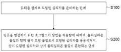
도 1은 본 발명의 실시예에 따른 단결정성 실리콘 잉곳을 형성하기 위한 순서도를 도시한다.Various objects and advantages of the present invention will become more readily apparent from the following detailed description when read in conjunction with the accompanying drawings.
1 shows a flow chart for forming a monocrystalline silicon ingot according to an embodiment of the present invention.
본 개시물과 그 이점의 좀 더 완벽한 이해를 위해, 첨부 도면과 함께 이하의 상세한 설명이 이제 참조되는데, 상기 도면에서 유사한 참조 번호는 유사한 특징부를 가리킨다. 기술 분야에서 통상의 기술을 가진 자는 본 명세서에 기술된 것을 포함하여 예시 실시예를 실행하기 위한 다른 변형예를 이해할 것이다. 도면은 특정 스케일로 제한되지 않고, 유사한 참조 번호는 유사한 요소를 나타내는데 사용된다. 개시물과 첨부된 청구항에서 사용되는 바와 같이, 용어 "예시 실시예", "예시적인 실시예" 및 "본 실시예"는 동일한 실시예를 언급하더라도 그럴 필요는 없고, 다양한 예시 실시예가 본 개시물의 범위나 사상에서 벗어남 없이 용이하게 결합되고 교환될 수 있다. 더구나, 본 명세서에 사용된 용어는 본 개시물의 한정사항으로 의도되지 않고, 단지 예시 실시예를 기술하기 위함이다. 이와 관련하여, 본 명세서에서 사용된 바와 같은, 용어 "이내(in)"는 "이내(in)" 및 "상(on)"을 포함하고, 용어 "하나", "하나의" 및 "그"는 단수와 복수 참조를 포함할 수 있다. 더구나, 본 명세서에서 사용된 바와 같이, 용어 "의하여(by)"는 문맥에 따라 "로부터(from)"도 의미할 수 있다. 더구나, 본 명세서에서 사용된 바와 같이, 용어 "만일"은 문맥에 따라 "때(when)" 또는 "하면(upon)"도 의미할 수 있다. 더구나, 본 명세서에서 사용된 바와 같이, 단어 "및/또는"은 관련하여 나열된 항목의 하나 이상의 모든 가능한 조합을 말하고 포함할 수 있다.BRIEF DESCRIPTION OF THE DRAWINGS For a more complete understanding of the present disclosure and advantages thereof, reference is now made to the following description, taken in conjunction with the accompanying drawings, in which like reference numerals refer to like features. Those of ordinary skill in the art will understand other modifications for carrying out the exemplary embodiments, including those described herein. The drawings are not limited to a particular scale, and like reference numerals are used to refer to like elements. As used in the disclosure and the appended claims, the terms "exemplary embodiment "," exemplary embodiment ", and "exemplary embodiment" are not necessarily to be construed to limit the present invention Can be easily combined and exchanged without departing from the scope or spirit. Moreover, the terminology used herein is not intended to be limiting of the disclosure, but is for the purpose of describing exemplary embodiments only. In this regard, as used herein, the term "in" includes "in" and "on," and the terms "one," " May include singular and plural references. Moreover, as used herein, the term " by "may also mean" from "depending on the context. Moreover, as used herein, the term "if" can also mean " when "or" upon "depending on the context. Moreover, as used herein, the words "and / or" may refer to and include one or more all possible combinations of the listed items in relation.
본 발명의 실시예에 따르면, 단결정성 실리콘 잉곳을 형성하기 위한 방법이 제공된다. 본 방법은 듀테륨 원자로 도핑된 실리카를 준비하는 단계 S100; 및 잉곳을 형성하기 위한 초크랄스키 방법을 적용함에 의하여, 폴리실리콘 물질과 함께 원시 도핑 물질로서 도핑된 실리카를 용융시키는 단계 S200 - 상기 도핑된 실리카와 상기 폴리실리콘 물질은 혼합됨 - 를 포함한다.According to an embodiment of the present invention, a method for forming a monocrystalline silicon ingot is provided. The method includes the steps of: preparing S100 doped silica; And melting the doped silica as a raw doping material together with the polysilicon material by applying the Czochralski method to form the ingot S200, wherein the doped silica and the polysilicon material are mixed.
단계 S100에서, 실리카는 단결정성 실리콘, 불순물이 있는 실리카등으로부터 선택될 수 있다. 초크랄스키 방법이 적용되기 이전에, 실리카는 듀테륨 원자로 도핑되어서 그 사이에 침입형 듀테륨 원자를 형성한다. 그리고 나서, 실리카 내의 산소와 다른 불순물의 함량이 감소되어서, 잉곳에 의해 생성되는 웨이퍼(들)를 통해 형성된 반도체 장치의 성능과 신뢰성을 향상시키기 위한 가능성을 높인다. 더구나, 듀테륨 원자로 실리카를 도핑할 때, 가령, 듀테륨 원자의 투여량은 1E12~1E18 ions/cm2 및 바람직하게는 1E15 ions/cm2일 수 있다.In step S100, the silica may be selected from monocrystalline silicon, impurity-containing silica, and the like. Before the Czochralski method is applied, silica is doped with a deuterium atom to form an interstitial deuterium atom therebetween. The content of oxygen and other impurities in the silica is then reduced to increase the likelihood of improving the performance and reliability of the semiconductor device formed through the wafer (s) produced by the ingot. Also, when doped with a deuterium atom silica, for example, the dosage of deuterium atoms may be 1E12 ~ 1E18 ions / cm2, and preferably 1E15 ions / cm2.
더구나, 듀테륨 원자로 실리카를 도핑할 때, 듀테륨 원자의 에너지는 1keV~100keV일 수 있고, 바람직하게는 50keV일 수 있다. 특정한 에너지 또는 투여량은 실리카의 크기에 따라 가변될 수 있다는 점에 유의한다.Moreover, when doping the deuterium atomic silica, the energy of the deuterium atom can be 1 keV to 100 keV, preferably 50 keV. It should be noted that the specific energy or dose may vary depending on the size of the silica.
단계 S200에서, 도핑된 실리카는 잉곳을 형성하기 위한 초크랄스키 방법을 위한 원시 도핑 물질로서의 역할을 한다. 구체적으로, 초크랄스키 방법은, 사전 결정된 온도에서 폴리실리콘 물질과 함께 용융될 도핑된 실리카를 도가니에 넣는 단계와, 용융된 물질내에 담겨진 시드 결정을 사전 결정된 당김 속도(pull rate)로 당겨서 단결정을 성장시키고, 단결정의 목 길이(neck length)가 사전 결정된 길이에 도달할 때 어깨 단계(shoulder stage)로 전이시키기 위해 당김 속도를 늦추는 단계; 어깨 단계에서 느려진 당김 속도로 선형 냉각 속도를 유지하여 잉곳에 대한 사전 결정된 지름을 형성하고, 일정한 지름 성장 단계로 전이시키는 단계; 및 잉곳의 지름이 사전 결정된 지름에 도달할 때, 선형 냉각을 중지하지만 냉각으로 빠르게 단결정을 당기고, 올림 속도(lifting rate)로 도가니를 올리며, 지름 가변 속도(diameter variety rate)에 따라 당김 속도를 서서히 조절하고, 잉곳의 지름을 안정화시킨 이후에 자동 일정한 지름 성장 단계로 전이하기 위해 자동 일정한 지름 성장 프로그램을 실행하는 단계를 더 포함할 수 있다. 더구나, 잉곳의 지름은 선택적으로 당김 속도 및 사전 결정된 온도를 통해 제어될 수 있고, 공정 요구사항에 따라 설계될 수 있다.In step S200, the doped silica serves as a raw doping material for the Czochralski method to form the ingot. Specifically, the Czochralski method comprises the steps of placing a doped silica to be melted together with a polysilicon material at a predetermined temperature into a crucible, and pulling the seed crystal contained in the molten material at a predetermined pull rate to form a single crystal Slowing the pulling rate to transition to a shoulder stage when the neck length of the single crystal reaches a predetermined length; Maintaining a linear cooling rate at a slow pulling speed in a shoulder step to form a predetermined diameter for the ingot and transitioning to a constant diameter growth step; And when the diameter of the ingot reaches a predetermined diameter, the linear cooling is stopped, but the cooling is rapidly pulled by the single crystal, the crucible is lifted at the lifting rate, and the pulling rate is gradually increased according to the diameter variety rate And performing an automatic constant diameter growth program to transition to an automatic constant diameter growth step after stabilizing the diameter of the ingot. Moreover, the diameter of the ingot can optionally be controlled through pulling speed and predetermined temperature, and can be designed according to process requirements.
본 발명에 따르면, 단결정성 실리콘 웨이퍼를 형성하기 위한 방법이 더욱 제공된다. 상기 언급된 방법에 따라 형성된 잉곳이 재료로 사용되어서 웨이퍼를 형성한다. 구체적으로, 슬라이싱, 그라인딩, 폴리싱, 표면 프로파일링 및 세척의 추가 단계가 잉곳을 웨이퍼로 변화시키기 위해 실행될 수 잇다. 그리고 나서, 반도체 장치는 웨이퍼상에 형성될 수 있다. 침입된 장소내에 수용된 듀테륨 원자 및 웨이퍼 내의 산소 원자와 다른 불순물의 낮은 함량 때문에, 열 공정에서 대개 발생하는 산소 침전은 현저하게 감소되어서, 장치 활성 영역에서 게이트 산화물의 무결성을 보호하고 원치 않은 누설 전류를 피할 수 있다.According to the present invention, a method for forming a monocrystalline silicon wafer is further provided. The ingot formed according to the above-mentioned method is used as a material to form a wafer. Specifically, additional steps of slicing, grinding, polishing, surface profiling and cleaning can be performed to change the ingot into a wafer. Then, the semiconductor device can be formed on the wafer. Owing to the low content of deuterium atoms and other oxygen atoms and other impurities contained in the intruded sites, the oxygen precipitation that usually occurs in the thermal process is significantly reduced to protect the integrity of the gate oxide in the device active region, Can be avoided.
요약하면, 본 발명에 따른 실시예의 단결정성 실리콘 잉곳과 웨이퍼를 형성하기 위한 방법에서, 잉곳 내에서 혼합된 산소와 다른 불순물의 함량은 감소될 수 있고, 이는 초크랄스키 방법에서 잉곳을 형성하기 위한 원시 도핑 물질로서, 침입형 듀테륨 원자로 도핑된 실리카에서 오고, 핫 캐리어에 대한 저항성을 강화하고, 누설 전류를 낮추며 반도체 장치의 성능과 신뢰성을 개선하는데, 이는 반도체 장치를 형성하기 위한 공정에서 침입형 듀테륨 원자가 확산되어서 댕글링 본드에 부착됨에 의한, 댕글링 본드의 감소에 기인한다.In summary, in a method for forming a wafer with a monocrystalline silicon ingot in an embodiment according to the present invention, the content of oxygen and other impurities mixed in the ingot can be reduced, which is advantageous for forming ingots in the Czochralski process As a raw doping material, it comes from silica doped with an interstitial deuterium atom, enhances resistance to hot carriers, lowers leakage currents and improves the performance and reliability of semiconductor devices, Due to the reduction of the dangling bonds due to the diffusion of the atoms and attachment to the dangling bonds.
개시된 원리에 따른 다양한 실시예가 상기에 기술되지만, 이들은 단지 예시로서 제시되는 것이지 제한하는 것이 아니라는 것을 이해해야 한다. 따라서, 예시적 실시예(들)의 너비와 범위는 상기 기술된 임의의 실시예에 의해 제한되어서는 아니되고, 청구항 및 본 개시물에서 나온 이들의 등가예에 따라서만 정의되어야 한다. 더구나, 상기 이점 및 특징은 기술된 실시예에서 제공되나, 이러한 문제가 된 청구항의 상기 이점의 일부나 전부를 달성하는 공정 및 구조로의 적용을 제한해서는 아니된다.While various embodiments in accordance with the disclosed principles are described above, it should be understood that they have been presented by way of example only, and not limitation. Thus, the breadth and scope of the exemplary embodiment (s) should not be limited by any of the above-described embodiments, but should be defined only in accordance with the claims and their equivalents from the disclosure. Moreover, the benefits and features are provided in the described embodiments, but should not limit the application to processes and structures that achieve some or all of the benefits of the problem in question.
또한, 본 명세서의 섹션 제목은 37 C.F.R 1.77하의 제안에 준수하여 제공되거나, 아니면 조직적인 큐를 제공한다. 이들 제목은 본 개시물에서 나올 수 있는 임의의 청구항에서 나온 발명을 제한하거나 특징 지을 수 없다. 구체적으로, "배경 기술"에서의 기술의 설명은 이러한 기술이 본 개시물에서의 발명의 종래 기술이라는 인정으로 해석되지 않는다. 더구나, 본 개시물에서 단수로 "발명"으로의 임의의 언급은 본 개시물에서 신규성의 단일점만이 있다고 주장하는데 사용되어서는 아니된다. 복수의 발명은 본 개시물로부터 나온 복수의 청구항의 제한에 따라 제시될 수 있고, 따라서 이러한 청구항은 발명(들), 및 따라서 보호되는 이들의 등가예를 정의한다. 모든 예시에서, 이러한 청구항의 범위는 본 개시물의 관점에서 자체적인 장벙으로 해석되어야 하고, 본 명세서의 제목에 의해 제약되어서는 아니된다.In addition, the section headings in this specification are provided in compliance with the proposals under 37 C.F.R 1.77, or provide a systematic queue. These headings can not limit or characterize the invention from any claim that may come from this disclosure. Specifically, the description of the technique in the "background art" is not to be construed as an admission that such a technique is prior art to the invention in this disclosure. Moreover, any reference in this disclosure to the "invention" in the singular should not be used to say that there is a single point of novelty in this disclosure. A plurality of inventions may be suggested in accordance with the limitations of the claims from the present disclosure, and such claims define the invention (s), and therefore equivalents thereof, to be protected. In all instances, the scope of such claims should be construed in their spirit in light of this disclosure, and should not be limited by the title of this specification.
Claims (9)
Translated fromKorean듀테륨 원자로 도핑된 실리카를 준비하는 단계와,
잉곳을 형성하기 위한 초크랄스키 방법을 적용함에 의하여, 폴리실리콘 물질과 함께 원시 도핑 물질로서 도핑된 실리카를 용융시키는 단계 - 상기 도핑된 실리카와 상기 폴리실리콘 물질은 혼합됨 - 를 포함하는, 단결정성 실리콘 잉곳을 형성하기 위한 방법.A method for forming a monocrystalline silicon ingot,
Preparing a deuterium-doped silica,
Melting a doped silica as a raw doping material together with a polysilicon material by applying a Czochralski method for forming an ingot, wherein the doped silica and the polysilicon material are mixed, A method for forming a silicon ingot.
사전 결정된 온도에서 도가니 내의 폴리실리콘 물질과 함께 도핑된 실리카를 용융시키는 단계와,
용융된 폴리실리콘 조각내에 담겨진 시드 결정을 사전 결정된 당김 속도(pull rate)로 당겨서 단결정을 성장시키고, 단결정의 목 길이(neck length)가 사전 결정된 길이에 도달할 때 어깨 단계(shoulder stage)로 전이시키기 위해 당김 속도를 늦추는 단계;
어깨 단계에서 느려진 당김 속도로 선형 냉각 속도를 유지하여 잉곳에 대한 사전 결정된 지름을 형성하고, 일정한 지름 성장 단계로 전이시키는 단계; 및
잉곳의 지름이 사전 결정된 지름에 도달할 때, 선형 냉각을 중지하지만 냉각으로 빠르게 단결정을 당기고, 올림 속도(lifting rate)로 도가니를 올리며, 지름 가변 속도(diameter variety rate)에 따라 당김 속도를 서서히 조절하고, 잉곳의 지름을 안정화시킨 이후에 자동 일정한 지름 성장 단계로 전이하기 위해 자동 일정한 지름 성장 프로그램을 실행하는 단계를 더 포함하는 것을 특징으로 하는 단결정성 실리콘 잉곳을 형성하기 위한 방법.The method of claim 1, wherein the Czochralski method comprises:
Melting the doped silica with the polysilicon material in the crucible at a predetermined temperature,
The seed crystal contained in the molten polysilicon slice is pulled at a predetermined pull rate to grow a single crystal and the transition to the shoulder stage when the neck length of the single crystal reaches a predetermined length Slowing the pulling speed;
Maintaining a linear cooling rate at a slow pulling speed in a shoulder step to form a predetermined diameter for the ingot and transitioning to a constant diameter growth step; And
When the diameter of the ingot reaches a predetermined diameter, the linear cooling is stopped, but the cooling rapidly pulls the single crystal, raises the crucible at the lifting rate, and slowly adjusts the pulling speed according to the diameter variety rate And performing an automatic constant diameter growth program to transition to an automatic constant diameter growth step after stabilizing the diameter of the ingot. ≪ Desc / Clms Page number 13 >
Applications Claiming Priority (2)
| Application Number | Priority Date | Filing Date | Title |
|---|---|---|---|
| CN201510672144.6ACN106591944B (en) | 2015-10-15 | 2015-10-15 | The forming method of monocrystal silicon and wafer |
| CN201510672144.6 | 2015-10-15 |
Publications (2)
| Publication Number | Publication Date |
|---|---|
| KR20170044583Atrue KR20170044583A (en) | 2017-04-25 |
| KR101902629B1 KR101902629B1 (en) | 2018-09-28 |
Family
ID=58456649
Family Applications (1)
| Application Number | Title | Priority Date | Filing Date |
|---|---|---|---|
| KR1020160122925AActiveKR101902629B1 (en) | 2015-10-15 | 2016-09-26 | Method for forming monocrystalline silicon ingot and wafers |
Country Status (6)
| Country | Link |
|---|---|
| US (1) | US20170107640A1 (en) |
| JP (1) | JP2017075084A (en) |
| KR (1) | KR101902629B1 (en) |
| CN (1) | CN106591944B (en) |
| DE (1) | DE102016118224A1 (en) |
| TW (1) | TWI589737B (en) |
Families Citing this family (1)
| Publication number | Priority date | Publication date | Assignee | Title |
|---|---|---|---|---|
| CN106591939A (en)* | 2015-10-15 | 2017-04-26 | 上海新昇半导体科技有限公司 | Monocrystalline silicon ingot and wafer forming method |
Family Cites Families (19)
| Publication number | Priority date | Publication date | Assignee | Title |
|---|---|---|---|---|
| US4092405A (en)* | 1976-06-01 | 1978-05-30 | Avco Everett Research Laboratory, Inc. | Separation of deuterium from hydrogen |
| JPH05294789A (en)* | 1992-04-20 | 1993-11-09 | Toshiba Corp | Method for pulling up silicon crystal |
| JP2000323443A (en)* | 1999-05-14 | 2000-11-24 | Mitsubishi Materials Silicon Corp | Manufacture of semiconductor wafer |
| US6285011B1 (en)* | 1999-10-12 | 2001-09-04 | Memc Electronic Materials, Inc. | Electrical resistance heater for crystal growing apparatus |
| JP2004035353A (en)* | 2002-07-05 | 2004-02-05 | Sumitomo Mitsubishi Silicon Corp | Process for preparing silicon single crystal |
| JP5023451B2 (en)* | 2004-08-25 | 2012-09-12 | 株式会社Sumco | Silicon wafer manufacturing method, silicon single crystal growth method |
| US7148124B1 (en)* | 2004-11-18 | 2006-12-12 | Alexander Yuri Usenko | Method for forming a fragile layer inside of a single crystalline substrate preferably for making silicon-on-insulator wafers |
| JP4821179B2 (en)* | 2005-06-20 | 2011-11-24 | 株式会社Sumco | Method for growing silicon single crystal |
| JP4862290B2 (en)* | 2005-06-20 | 2012-01-25 | 株式会社Sumco | Silicon single crystal manufacturing method |
| JP4806974B2 (en)* | 2005-06-20 | 2011-11-02 | 株式会社Sumco | Silicon single crystal growth method |
| EP1981065B1 (en)* | 2005-12-27 | 2014-12-03 | Shin-Etsu Chemical Company, Ltd. | Process for producing soi wafer |
| JP4760729B2 (en)* | 2006-02-21 | 2011-08-31 | 株式会社Sumco | Silicon single crystal wafer for IGBT and manufacturing method of silicon single crystal wafer for IGBT |
| US20080050879A1 (en)* | 2006-08-23 | 2008-02-28 | Taiwan Semiconductor Manufacturing Co., Ltd. | Methods of forming metal-containing gate structures |
| US8262797B1 (en)* | 2007-03-13 | 2012-09-11 | Solaicx, Inc. | Weir design providing optimal purge gas flow, melt control, and temperature stabilization for improved single crystal growth in a continuous Czochralski process |
| US20090162970A1 (en)* | 2007-12-20 | 2009-06-25 | Yang Michael X | Material modification in solar cell fabrication with ion doping |
| CN101435105A (en)* | 2008-12-01 | 2009-05-20 | 浙江碧晶科技有限公司 | Method for preparing low oxygen content silicon crystal |
| JP2010141272A (en)* | 2008-12-15 | 2010-06-24 | Sumco Corp | Epitaxial wafer and its production method |
| US8545623B2 (en)* | 2009-06-18 | 2013-10-01 | Sumco Phoenix Corporation | Method and apparatus for controlling the growth process of a monocrystalline silicon ingot |
| JP2012140285A (en)* | 2010-12-28 | 2012-07-26 | Siltronic Japan Corp | Method for producing silicon single crystal ingot |
- 2015
- 2015-10-15CNCN201510672144.6Apatent/CN106591944B/enactiveActive
- 2016
- 2016-03-14TWTW105107811Apatent/TWI589737B/enactive
- 2016-06-09USUS15/178,080patent/US20170107640A1/ennot_activeAbandoned
- 2016-06-22JPJP2016123431Apatent/JP2017075084A/enactivePending
- 2016-09-26KRKR1020160122925Apatent/KR101902629B1/enactiveActive
- 2016-09-27DEDE102016118224.9Apatent/DE102016118224A1/ennot_activeCeased
Also Published As
| Publication number | Publication date |
|---|---|
| TWI589737B (en) | 2017-07-01 |
| DE102016118224A1 (en) | 2017-04-20 |
| TW201713801A (en) | 2017-04-16 |
| US20170107640A1 (en) | 2017-04-20 |
| JP2017075084A (en) | 2017-04-20 |
| CN106591944B (en) | 2018-08-24 |
| CN106591944A (en) | 2017-04-26 |
| KR101902629B1 (en) | 2018-09-28 |
Similar Documents
| Publication | Publication Date | Title |
|---|---|---|
| CN100472001C (en) | Silicon wafer, SOI substrate, silicon single crystal growth method, silicon wafer manufacturing method and SOI substrate manufacturing method | |
| JP6142054B1 (en) | Method for growing single crystal silicon | |
| DE112014002781B9 (en) | Process for controlling oxygen precipitation in heavily doped silicon wafers, cut from ingots grown according to the Czochralski process, and silicon wafers | |
| CN105900219A (en) | Silicon wafer and method for producing same | |
| US9303332B2 (en) | Silicon single crystal substrate and method of manufacturing the same | |
| SG189506A1 (en) | Method of manufacturing silicon single crystal, silicon single crystal, and wafer | |
| TWI628317B (en) | Method for growing monocrystalline silicon by using czochralski method | |
| KR101902629B1 (en) | Method for forming monocrystalline silicon ingot and wafers | |
| KR101865467B1 (en) | Method for forming monocrystalline silicon ingot and wafer | |
| US10100431B2 (en) | Method for growing monocrystalline silicon and monocrystalline silicon ingot prepared thereof | |
| TW201623703A (en) | Method of fabrication of an ingot of n-type single-crystal silicon with a controlled concentration of oxygen-based thermal donors | |
| TWI628316B (en) | Methods for forming monocrystalline silicon ingot and wafer | |
| KR102429972B1 (en) | High resistivity wafer manufacturing method | |
| KR102737899B1 (en) | Method for manufacturing silicon single crystals | |
| JPS59102891A (en) | Preparation of silicon single crystal | |
| Abe et al. | the history of silicon single crystals and then CZ (Czochralski) crystal growth technology has followed it at the same time of | |
| CN107154353B (en) | Method for heat treatment of wafer | |
| Abe et al. | the history of silicon single crystals and then CZ (Czochralski) | |
| Abe | the IC (integrated circuit) invention. Controls of dopants (BР) and light elements (CNO), elimination of heavy metals (Cu, Fe) have been done but a behavior of the point defects has | |
| KR20060072691A (en) | Silicon Wafer and Manufacturing Method Thereof | |
| KR20130097924A (en) | Single crystal silicon ingot growing method, single crystal silicon ingot, and epitaxial silicon wafer | |
| KR20020093689A (en) | Silicon wafer having controlled distribution of defects, process for the preparation of the same |
Legal Events
| Date | Code | Title | Description |
|---|---|---|---|
| A201 | Request for examination | ||
| PA0109 | Patent application | Patent event code:PA01091R01D Comment text:Patent Application Patent event date:20160926 | |
| PA0201 | Request for examination | ||
| PG1501 | Laying open of application | ||
| E902 | Notification of reason for refusal | ||
| PE0902 | Notice of grounds for rejection | Comment text:Notification of reason for refusal Patent event date:20170830 Patent event code:PE09021S01D | |
| E902 | Notification of reason for refusal | ||
| PE0902 | Notice of grounds for rejection | Comment text:Notification of reason for refusal Patent event date:20180226 Patent event code:PE09021S01D | |
| E701 | Decision to grant or registration of patent right | ||
| PE0701 | Decision of registration | Patent event code:PE07011S01D Comment text:Decision to Grant Registration Patent event date:20180822 | |
| GRNT | Written decision to grant | ||
| PR0701 | Registration of establishment | Comment text:Registration of Establishment Patent event date:20180919 Patent event code:PR07011E01D | |
| PR1002 | Payment of registration fee | Payment date:20180919 End annual number:3 Start annual number:1 | |
| PG1601 | Publication of registration | ||
| PR1001 | Payment of annual fee | Payment date:20210728 Start annual number:4 End annual number:4 | |
| PR1001 | Payment of annual fee | Payment date:20220706 Start annual number:5 End annual number:5 | |
| PR1001 | Payment of annual fee | Payment date:20250626 Start annual number:8 End annual number:8 |