KR20170037503A - The organic light emitting display device and manufacturing method, using the organic light emitting display electronics devices - Google Patents
The organic light emitting display device and manufacturing method, using the organic light emitting display electronics devicesDownload PDFInfo
- Publication number
- KR20170037503A KR20170037503AKR1020160099570AKR20160099570AKR20170037503AKR 20170037503 AKR20170037503 AKR 20170037503AKR 1020160099570 AKR1020160099570 AKR 1020160099570AKR 20160099570 AKR20160099570 AKR 20160099570AKR 20170037503 AKR20170037503 AKR 20170037503A
- Authority
- KR
- South Korea
- Prior art keywords
- light emitting
- organic light
- emitting display
- adhesive layer
- display panel
- Prior art date
- Legal status (The legal status is an assumption and is not a legal conclusion. Google has not performed a legal analysis and makes no representation as to the accuracy of the status listed.)
- Ceased
Links
Images


Classifications
- H—ELECTRICITY
- H10—SEMICONDUCTOR DEVICES; ELECTRIC SOLID-STATE DEVICES NOT OTHERWISE PROVIDED FOR
- H10K—ORGANIC ELECTRIC SOLID-STATE DEVICES
- H10K59/00—Integrated devices, or assemblies of multiple devices, comprising at least one organic light-emitting element covered by group H10K50/00
- H10K59/40—OLEDs integrated with touch screens
- H01L27/323—
- G—PHYSICS
- G02—OPTICS
- G02F—OPTICAL DEVICES OR ARRANGEMENTS FOR THE CONTROL OF LIGHT BY MODIFICATION OF THE OPTICAL PROPERTIES OF THE MEDIA OF THE ELEMENTS INVOLVED THEREIN; NON-LINEAR OPTICS; FREQUENCY-CHANGING OF LIGHT; OPTICAL LOGIC ELEMENTS; OPTICAL ANALOGUE/DIGITAL CONVERTERS
- G02F1/00—Devices or arrangements for the control of the intensity, colour, phase, polarisation or direction of light arriving from an independent light source, e.g. switching, gating or modulating; Non-linear optics
- G02F1/01—Devices or arrangements for the control of the intensity, colour, phase, polarisation or direction of light arriving from an independent light source, e.g. switching, gating or modulating; Non-linear optics for the control of the intensity, phase, polarisation or colour
- G02F1/13—Devices or arrangements for the control of the intensity, colour, phase, polarisation or direction of light arriving from an independent light source, e.g. switching, gating or modulating; Non-linear optics for the control of the intensity, phase, polarisation or colour based on liquid crystals, e.g. single liquid crystal display cells
- G02F1/133—Constructional arrangements; Operation of liquid crystal cells; Circuit arrangements
- G02F1/1333—Constructional arrangements; Manufacturing methods
- G02F1/13338—Input devices, e.g. touch panels
- G—PHYSICS
- G06—COMPUTING OR CALCULATING; COUNTING
- G06F—ELECTRIC DIGITAL DATA PROCESSING
- G06F3/00—Input arrangements for transferring data to be processed into a form capable of being handled by the computer; Output arrangements for transferring data from processing unit to output unit, e.g. interface arrangements
- G06F3/01—Input arrangements or combined input and output arrangements for interaction between user and computer
- G06F3/03—Arrangements for converting the position or the displacement of a member into a coded form
- G06F3/041—Digitisers, e.g. for touch screens or touch pads, characterised by the transducing means
- G06F3/0412—Digitisers structurally integrated in a display
- G—PHYSICS
- G06—COMPUTING OR CALCULATING; COUNTING
- G06F—ELECTRIC DIGITAL DATA PROCESSING
- G06F3/00—Input arrangements for transferring data to be processed into a form capable of being handled by the computer; Output arrangements for transferring data from processing unit to output unit, e.g. interface arrangements
- G06F3/01—Input arrangements or combined input and output arrangements for interaction between user and computer
- G06F3/03—Arrangements for converting the position or the displacement of a member into a coded form
- G06F3/041—Digitisers, e.g. for touch screens or touch pads, characterised by the transducing means
- G06F3/0414—Digitisers, e.g. for touch screens or touch pads, characterised by the transducing means using force sensing means to determine a position
- G06F3/04142—Digitisers, e.g. for touch screens or touch pads, characterised by the transducing means using force sensing means to determine a position the force sensing means being located peripherally, e.g. disposed at the corners or at the side of a touch sensing plate
- G—PHYSICS
- G06—COMPUTING OR CALCULATING; COUNTING
- G06F—ELECTRIC DIGITAL DATA PROCESSING
- G06F3/00—Input arrangements for transferring data to be processed into a form capable of being handled by the computer; Output arrangements for transferring data from processing unit to output unit, e.g. interface arrangements
- G06F3/01—Input arrangements or combined input and output arrangements for interaction between user and computer
- G06F3/03—Arrangements for converting the position or the displacement of a member into a coded form
- G06F3/041—Digitisers, e.g. for touch screens or touch pads, characterised by the transducing means
- G06F3/0416—Control or interface arrangements specially adapted for digitisers
- G—PHYSICS
- G09—EDUCATION; CRYPTOGRAPHY; DISPLAY; ADVERTISING; SEALS
- G09G—ARRANGEMENTS OR CIRCUITS FOR CONTROL OF INDICATING DEVICES USING STATIC MEANS TO PRESENT VARIABLE INFORMATION
- G09G3/00—Control arrangements or circuits, of interest only in connection with visual indicators other than cathode-ray tubes
- G09G3/001—Control arrangements or circuits, of interest only in connection with visual indicators other than cathode-ray tubes using specific devices not provided for in groups G09G3/02 - G09G3/36, e.g. using an intermediate record carrier such as a film slide; Projection systems; Display of non-alphanumerical information, solely or in combination with alphanumerical information, e.g. digital display on projected diapositive as background
- G09G3/003—Control arrangements or circuits, of interest only in connection with visual indicators other than cathode-ray tubes using specific devices not provided for in groups G09G3/02 - G09G3/36, e.g. using an intermediate record carrier such as a film slide; Projection systems; Display of non-alphanumerical information, solely or in combination with alphanumerical information, e.g. digital display on projected diapositive as background to produce spatial visual effects
- G—PHYSICS
- G09—EDUCATION; CRYPTOGRAPHY; DISPLAY; ADVERTISING; SEALS
- G09G—ARRANGEMENTS OR CIRCUITS FOR CONTROL OF INDICATING DEVICES USING STATIC MEANS TO PRESENT VARIABLE INFORMATION
- G09G3/00—Control arrangements or circuits, of interest only in connection with visual indicators other than cathode-ray tubes
- G09G3/20—Control arrangements or circuits, of interest only in connection with visual indicators other than cathode-ray tubes for presentation of an assembly of a number of characters, e.g. a page, by composing the assembly by combination of individual elements arranged in a matrix no fixed position being assigned to or needed to be assigned to the individual characters or partial characters
- G09G3/22—Control arrangements or circuits, of interest only in connection with visual indicators other than cathode-ray tubes for presentation of an assembly of a number of characters, e.g. a page, by composing the assembly by combination of individual elements arranged in a matrix no fixed position being assigned to or needed to be assigned to the individual characters or partial characters using controlled light sources
- G09G3/30—Control arrangements or circuits, of interest only in connection with visual indicators other than cathode-ray tubes for presentation of an assembly of a number of characters, e.g. a page, by composing the assembly by combination of individual elements arranged in a matrix no fixed position being assigned to or needed to be assigned to the individual characters or partial characters using controlled light sources using electroluminescent panels
- G09G3/32—Control arrangements or circuits, of interest only in connection with visual indicators other than cathode-ray tubes for presentation of an assembly of a number of characters, e.g. a page, by composing the assembly by combination of individual elements arranged in a matrix no fixed position being assigned to or needed to be assigned to the individual characters or partial characters using controlled light sources using electroluminescent panels semiconductive, e.g. using light-emitting diodes [LED]
- G09G3/3208—Control arrangements or circuits, of interest only in connection with visual indicators other than cathode-ray tubes for presentation of an assembly of a number of characters, e.g. a page, by composing the assembly by combination of individual elements arranged in a matrix no fixed position being assigned to or needed to be assigned to the individual characters or partial characters using controlled light sources using electroluminescent panels semiconductive, e.g. using light-emitting diodes [LED] organic, e.g. using organic light-emitting diodes [OLED]
- G09G3/3225—Control arrangements or circuits, of interest only in connection with visual indicators other than cathode-ray tubes for presentation of an assembly of a number of characters, e.g. a page, by composing the assembly by combination of individual elements arranged in a matrix no fixed position being assigned to or needed to be assigned to the individual characters or partial characters using controlled light sources using electroluminescent panels semiconductive, e.g. using light-emitting diodes [LED] organic, e.g. using organic light-emitting diodes [OLED] using an active matrix
- G09G3/3233—Control arrangements or circuits, of interest only in connection with visual indicators other than cathode-ray tubes for presentation of an assembly of a number of characters, e.g. a page, by composing the assembly by combination of individual elements arranged in a matrix no fixed position being assigned to or needed to be assigned to the individual characters or partial characters using controlled light sources using electroluminescent panels semiconductive, e.g. using light-emitting diodes [LED] organic, e.g. using organic light-emitting diodes [OLED] using an active matrix with pixel circuitry controlling the current through the light-emitting element
- H—ELECTRICITY
- H10—SEMICONDUCTOR DEVICES; ELECTRIC SOLID-STATE DEVICES NOT OTHERWISE PROVIDED FOR
- H10K—ORGANIC ELECTRIC SOLID-STATE DEVICES
- H10K50/00—Organic light-emitting devices
- H10K50/80—Constructional details
- H10K50/84—Passivation; Containers; Encapsulations
- H10K50/841—Self-supporting sealing arrangements
- H—ELECTRICITY
- H10—SEMICONDUCTOR DEVICES; ELECTRIC SOLID-STATE DEVICES NOT OTHERWISE PROVIDED FOR
- H10K—ORGANIC ELECTRIC SOLID-STATE DEVICES
- H10K59/00—Integrated devices, or assemblies of multiple devices, comprising at least one organic light-emitting element covered by group H10K50/00
- H10K59/10—OLED displays
- H10K59/12—Active-matrix OLED [AMOLED] displays
- H10K59/131—Interconnections, e.g. wiring lines or terminals
- H10K59/1315—Interconnections, e.g. wiring lines or terminals comprising structures specially adapted for lowering the resistance
- H—ELECTRICITY
- H10—SEMICONDUCTOR DEVICES; ELECTRIC SOLID-STATE DEVICES NOT OTHERWISE PROVIDED FOR
- H10K—ORGANIC ELECTRIC SOLID-STATE DEVICES
- H10K59/00—Integrated devices, or assemblies of multiple devices, comprising at least one organic light-emitting element covered by group H10K50/00
- H10K59/80—Constructional details
- H10K59/87—Passivation; Containers; Encapsulations
- H10K59/871—Self-supporting sealing arrangements
- H10K59/872—Containers
- G—PHYSICS
- G06—COMPUTING OR CALCULATING; COUNTING
- G06F—ELECTRIC DIGITAL DATA PROCESSING
- G06F2203/00—Indexing scheme relating to G06F3/00 - G06F3/048
- G06F2203/041—Indexing scheme relating to G06F3/041 - G06F3/045
- G06F2203/04103—Manufacturing, i.e. details related to manufacturing processes specially suited for touch sensitive devices
- G—PHYSICS
- G06—COMPUTING OR CALCULATING; COUNTING
- G06F—ELECTRIC DIGITAL DATA PROCESSING
- G06F2203/00—Indexing scheme relating to G06F3/00 - G06F3/048
- G06F2203/041—Indexing scheme relating to G06F3/041 - G06F3/045
- G06F2203/04105—Pressure sensors for measuring the pressure or force exerted on the touch surface without providing the touch position
- G—PHYSICS
- G09—EDUCATION; CRYPTOGRAPHY; DISPLAY; ADVERTISING; SEALS
- G09G—ARRANGEMENTS OR CIRCUITS FOR CONTROL OF INDICATING DEVICES USING STATIC MEANS TO PRESENT VARIABLE INFORMATION
- G09G2300/00—Aspects of the constitution of display devices
- G09G2300/08—Active matrix structure, i.e. with use of active elements, inclusive of non-linear two terminal elements, in the pixels together with light emitting or modulating elements
- G09G2300/0809—Several active elements per pixel in active matrix panels
- G09G2300/0842—Several active elements per pixel in active matrix panels forming a memory circuit, e.g. a dynamic memory with one capacitor
- G—PHYSICS
- G09—EDUCATION; CRYPTOGRAPHY; DISPLAY; ADVERTISING; SEALS
- G09G—ARRANGEMENTS OR CIRCUITS FOR CONTROL OF INDICATING DEVICES USING STATIC MEANS TO PRESENT VARIABLE INFORMATION
- G09G2320/00—Control of display operating conditions
- G09G2320/06—Adjustment of display parameters
- G09G2320/0626—Adjustment of display parameters for control of overall brightness
- G09G2320/0646—Modulation of illumination source brightness and image signal correlated to each other
- H—ELECTRICITY
- H10—SEMICONDUCTOR DEVICES; ELECTRIC SOLID-STATE DEVICES NOT OTHERWISE PROVIDED FOR
- H10K—ORGANIC ELECTRIC SOLID-STATE DEVICES
- H10K2102/00—Constructional details relating to the organic devices covered by this subclass
- H10K2102/301—Details of OLEDs
- H10K2102/311—Flexible OLED
- H—ELECTRICITY
- H10—SEMICONDUCTOR DEVICES; ELECTRIC SOLID-STATE DEVICES NOT OTHERWISE PROVIDED FOR
- H10K—ORGANIC ELECTRIC SOLID-STATE DEVICES
- H10K59/00—Integrated devices, or assemblies of multiple devices, comprising at least one organic light-emitting element covered by group H10K50/00
- H10K59/10—OLED displays
- H10K59/12—Active-matrix OLED [AMOLED] displays
- H10K59/1201—Manufacture or treatment
Landscapes
- Engineering & Computer Science (AREA)
- Physics & Mathematics (AREA)
- Theoretical Computer Science (AREA)
- General Engineering & Computer Science (AREA)
- General Physics & Mathematics (AREA)
- Human Computer Interaction (AREA)
- Nonlinear Science (AREA)
- Optics & Photonics (AREA)
- Computer Hardware Design (AREA)
- Crystallography & Structural Chemistry (AREA)
- Chemical & Material Sciences (AREA)
- Mathematical Physics (AREA)
- Microelectronics & Electronic Packaging (AREA)
- Electroluminescent Light Sources (AREA)
- Devices For Indicating Variable Information By Combining Individual Elements (AREA)
Abstract
Translated fromKoreanDescription
Translated fromKorean본 발명은 유기 발광 표시 장치 및 그 제조 방법, 그리고 상기 유기 발광 표시 장치를 사용한 전자 기기에 관한 것이다.The present invention relates to an organic light emitting display, a method of manufacturing the same, and an electronic apparatus using the organic light emitting display.
현재, 새로운 세대의 터치 기술, 즉 터치 센싱 기술이 개발되면서 터치 장치는 가볍게 누르는 힘과 강하게 누르는 힘을 감지할 수 있고 대응되게 서로 다른 기능을 표시할 수 있다.Nowadays, as a new generation of touch technology, namely touch sensing technology, is developed, the touch device can sense the light pressing force and the strong pressing force and can display different functions correspondingly.
그러나 기존의 터치 장치는 일반적으로 압력 센서를 커버 플레이트 유리의 4개의 코너의 하방에 설치하여 힘의 크기와 인가되는 힘의 방향 및 위치를 판단한다. 이러한 제품에는 베젤의 폭을 협소시키지 못하고 설계상에서 별도의 처리가 필요되는 결점이 존재한다.However, in the conventional touch device, the pressure sensor is generally disposed below the four corners of the cover plate glass to determine the magnitude of the force and the direction and position of the applied force. These products have drawbacks in that the width of the bezel can not be narrowed and separate processing is required in the design.
관련기술에 존재하는 상기 문제 및/또는 기타 문제에 감안하여, 본 발명의 제1 양태에 따르면,In view of the above problems and / or other problems existing in the related art, according to the first aspect of the present invention,
터치 스크린과,With a touch screen,
상면이 상기 터치 스크린의 하면에 밀착되고, 하면에는 배면 점착층이 커버되게 설치되는 표시 패널과,A display panel in which an upper surface is in close contact with a lower surface of the touch screen and a lower surface adhesive layer is provided in a lower surface,
상면이 상기 배면 점착층에 점착되는 FPC(Flexible Printed Circuit)과,An FPC (Flexible Printed Circuit) whose upper surface is adhered to the backside adhesive layer,
상기 배면 점착층에 배치되는 복수개의 압력 센서를 포함하는 유기 발광 표시 장치가 제공된다.There is provided an organic light emitting display including a plurality of pressure sensors disposed on the backing adhesive layer.
바람직하게는, 상기 복수개의 압력 센서가 상기 FPC의 상면에 점착된다.Preferably, the plurality of pressure sensors are adhered to the upper surface of the FPC.
바람직하게는, 상기 표시 패널은 4개의 코너를 구비하고, 상기 4개의 코너 하방에는 각각 상기 압력 센서가 설치된다.Preferably, the display panel has four corners, and the pressure sensor is provided below each of the four corners.
바람직하게는, 상기 표시 패널의 상기 4개의 코너 하면이 상기 압력 센서에 접촉된다.Preferably, the four corner bottoms of the display panel are in contact with the pressure sensor.
바람직하게는, 상기 유기 발광 표시 장치는 AMOLED표시 장치이다.Preferably, the organic light emitting display device is an AMOLED display device.
바람직하게는, 상기 터치 스크린의 상면에 설치되는 1개의 투명한 커버 플레이트를 더 포함한다.Preferably, the touch screen further includes one transparent cover plate installed on the upper surface of the touch screen.
바람직하게는, 상기 투명한 커버 플레이트의 재질은 유리 또는 아크릴이다.Preferably, the material of the transparent cover plate is glass or acrylic.
본 발명의 제2 양태에 따르면,According to a second aspect of the present invention,
FPC및 복수개의 압력 센서를 제공하고, 상기 복수개의 압력 센서를 상기 FPC의 상면에 점착시키는 단계(1A)와,(1A) of providing an FPC and a plurality of pressure sensors, and adhering the plurality of pressure sensors to the upper surface of the FPC;
터치 스크린 및 표시 패널을 제공하고, 상기 터치 스크린의 하면을 상기 표시 패널의 상면에 밀착시키는 단계(1B)와,(1B) providing a touch screen and a display panel, and adhering the lower surface of the touch screen to the upper surface of the display panel;
상기 표시 패널의 하면에 배면 점착층을 밀착시키는 단계(1C)와,(1C) of adhering a rear surface adhesive layer to the lower surface of the display panel,
상기 FPC의 상면을 상기 배면 점착층의 하면에 점착시켜 상기 복수개의 압력 센서가 상기 배면 점착층에 삽입하도록 하는 단계(2)를 포함하는 유기 발광 표시 장치의 제조 방법이 제공된다.And a step (2) of adhering the upper surface of the FPC to the lower surface of the backing adhesive layer so that the plurality of pressure sensors are inserted into the backing adhesive layer.
바람직하게는, 상기 단계(2)에서, 상기 복수개의 압력 센서를, 상기 압력 센서가 상기 터치 스크린의 하면에 접촉할 때 까지 상기 배면 점착층에 삽입시킨다.Preferably, in the step (2), the plurality of pressure sensors are inserted into the backing adhesive layer until the pressure sensor contacts the lower surface of the touch screen.
바람직하게는, 상기 유기 발광 표시 장치는 AMOLED표시 장치이다.Preferably, the organic light emitting display device is an AMOLED display device.
본 발명의 제3 양태에 따르면,According to a third aspect of the present invention,
상기 유기 발광 표시 장치를 포함하는 전자 기기가 제공된다.An electronic device including the organic light emitting display device is provided.
본 발명의 유기 발광 표시 장치는 간단한 구조를 이용하여 압력 센서를 표시 패널의 하방에 설치하고 커버 플레이트 유리의 베젤 위치를 점하지 않아 커버 플레이트 유리의 베젤을 임의의 폭으로 축소할 수 있어 디스플레이의 비례를 증대시키고 사용자의 사용체험성을 강화시키고, 또한, 본 발명은 특히 AMOLED장치에 적용될 수 있다.INDUSTRIAL APPLICABILITY According to the OLED display of the present invention, the pressure sensor is disposed below the display panel by using a simple structure, and the bezel of the cover plate glass can be reduced to an arbitrary width without focusing on the position of the bezel of the cover plate glass. And the user's experience of use is enhanced. Further, the present invention can be applied to AMOLED devices in particular.
도 1은 본 발명의 실시예1에 따른 유기 발광 표시 장치의 단면구조를 나타내는 도면이다.
도 2는 본 발명의 실시예1에 따른 유기 발광 표시 장치의 평면구조를 나타내는 도면이다.
도 3은 실시예1의 유기 발광 표시 장치의 제조 방법의 단계(1A)을 나타내는 도면이다.
도 4는 실시예1의 유기 발광 표시 장치의 제조 방법의 단계(1C)를 나타내는 도면이다.
도 5는 실시예1의 유기 발광 표시 장치의 제조 방법의 단계(2)를 나타내는 도면이다.
도 6은 실시예2의 유기 발광 표시 장치의 단면구조를 나타내는 도면이다.1 is a view showing a cross-sectional structure of an organic light emitting diode display according to a first embodiment of the present invention.
2 is a view showing a planar structure of an OLED display according to a first embodiment of the present invention.
Fig. 3 is a view showing step (1A) of the manufacturing method of the organic light emitting display device according to the first embodiment.
Fig. 4 is a view showing step (1C) of the method of manufacturing the organic light emitting display device of Example 1. Fig.
5 is a view showing step (2) of the manufacturing method of the organic light emitting display device according to the first embodiment.
6 is a diagram showing a cross-sectional structure of an organic light emitting display device according to Embodiment 2. FIG.
첨부된 도면을 참조하면서 예시적인 실시양태에 대하여 더 전면적으로 설명한다. 그러나 본 발명은 예시적인 실시양태에 한정되는 것이 아니라, 예시적인 실시양태는 다양한 방식으로 실시될 수 있음이 이해되어야 한다. 이러한 실시양태를 제공하는 것은 본 발명이 전면적 및 완전해지도록 하는데 목적이 있으며 또한 예시적인 실시양태의 사상을 당업자에게 전면적으로 전달하기 위해서이다. 도면에서, 동일한 참조부호는 동일 또는 유사한 구조를 나타내므로 이에 대한 중복된 설명은 생략한다.BRIEF DESCRIPTION OF THE DRAWINGS Exemplary embodiments will now be described more fully with reference to the accompanying drawings. It should be understood, however, that the invention is not limited to the exemplary embodiments, but that the exemplary embodiments may be practiced in various ways. It is to be understood that providing such an embodiment is intended to provide a thorough and complete disclosure of the present invention, and also to convey to others skilled in the art the subject matter of the exemplary embodiments. In the drawings, the same reference numerals denote the same or similar structures, and a duplicate description thereof will be omitted.
설명된 특징, 구조 또는 특성은 임의의 적절한 방식을 통해 하나 또는 복수의 실시양태에 결합될 수 있다. 하기의 설명에서, 다양한 구체적인 세부 사항을 제공하여 본 발명의 실시양태를 충분히 이해하도록 한다. 그러나, 본 분야의 통상의 지식을 가진 에게 있어서, 세부 사항 중의 하나 또는 복수를 특정하는 것이 아니고, 다른 방법, 요소, 재료 등을 이용하여, 본 발명의 기술안을 실천할 수 있는 것이 자명하다. 어떤 상황에서는, 본 발명의 취지를 흐리지 않게 하기 위하여 공지 구조, 재료 또는 조작을 상세하게 예시 또는 설명하지 않는다.The described features, structures, or characteristics may be combined in any suitable manner into one or more embodiments. In the following description, numerous specific details are set forth to provide a thorough understanding of embodiments of the invention. However, it will be apparent to those skilled in the art that the techniques of the present invention can be practiced using other methods, elements, materials and the like, rather than specifying one or more of the details. In some circumstances, well-known structures, materials, or operations are not illustrated or described in detail in order not to obscure the spirit of the present invention.
본 발명의 도면은 단지 상대적 위치 관계 및 전기적 연결관계를 예시할 뿐이고, 어떤 부위 층의 두께는 이해의 편의상, 과다하게 예시되어 표현되었으나, 도면의 층의 두께는 실제적인 층의 두께의 비례관계를 의미하지 않는다.Although the drawings of the present invention merely illustrate relative positional and electrical connections, the thickness of any of the veneer layers has been excessively illustrated for ease of understanding, but the thickness of the layers in the figures is proportional to the thickness of the actual layer It does not mean.
실시예1Example 1
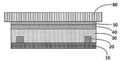
도 1은 본 발명의 실시예1에 따른 유기 발광 표시 장치의 구조를 나타내는 도면이고, 상기 유기 발광 표시 장치는, 터치 스크린(50)과, 표시 패널(40)과, 배면 점착층(30)과, FPC(10) 과, 복수개의 압력 센서(20)을 포함한다.1 is a view illustrating a structure of an organic light emitting display according to a first embodiment of the present invention. The organic light emitting display includes a
여기서, 표시 패널(40)의 상면이 터치 스크린(50)의 하면에 밀착되고, 표시 패널(40)의 하면에는 배면 점착층(30)이 커버되게 설치되며, FPC(10)의 상면이 배면 점착층(30)에 점착되고, 복수개의 압력 센서(20)는 배면 점착층(30)에 배치된다.The upper surface of the
본 실시예에서, 터치 스크린(50)의 위에는 투명한 커버 플레이트(60)가 설치되고 투명한 커버 플레이트(60)의 재질은 유리 또는 아크릴 등 일 수 있지만 본 발명은 이에 대해 한정하지 않는다.In this embodiment, the
바람직하게는, 도 1에 도시된 바와 같이, 복수개의 압력 센서(20)가 FPC(10)의 상면에 점착된다.Preferably, a plurality of
도 2는 유기 발광 표시 장치를 나타내는 평면도이고, 바람직하게는, 본 실시예에서, 상기 표시 장치는 구형이나 이에 한정하지 않는다. 도 2에는 표시 패널(40)이 투명한 커버 플레이트(60)의 하방에 설치되는 것이 도시되고, 표시 패널(40)은 4개의 코너를 구비하며, 4개의 코너의 하방의 각각에는 모두 하나의 압력 센서(20)가 설치된다. 따라서 힘의 크기 및 힘을 인가하는 방향과 위치를 더 정확하게 판단할 수 있다.2 is a plan view showing the organic light emitting diode display device. Preferably, in the present embodiment, the display device is spherical, but not limited thereto. 2, the
바람직하게는, 본 실시예의 유기 발광 표시 장치는 AMOLED표시 장치이다.Preferably, the organic light emitting display device of the present embodiment is an AMOLED display device.
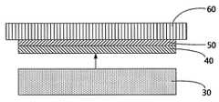
도 3 내지 도 5는 본 실시예의 유기 발광 표시 장치의 제조 과정을 나타내는 도면이다. 상기 제조 과정은 하기의 단계를 포함할 수 있다.FIGS. 3 to 5 are views showing a manufacturing process of the OLED display of the present embodiment. The manufacturing process may include the following steps.
단계(1A): 도 3에 도시된 바와 같이(화살이 가리키는 방향이 점착방향임. 하기에서도 동일함), FPC(10) 및 복수개의 압력 센서(20)을 제공하고, 복수개의 압력 센서(20)를 FPC(10)의 상면에 점착시킨다.Step 1A: As shown in Fig. 3 (the direction indicated by the arrow is the sticking direction). The
단계(1B): 터치 스크린(50) 및 표시 패널(40)을 제공하고, 터치 스크린(50)의 하면을 표시 패널(40)의 상면에 밀착시킨다.Step 1B: The
단계(1C): 도 4에 도시된 바와 같이, 표시 패널(40)의 하면에 배면 점착층(30)을 밀착시킨다.Step 1C: As shown in FIG. 4, the backside
참고로, 단계(1A), 단계(1B) 및 단계(1C)에서, 문자A, B, C는 단계의 선후순서를 가리키는 것이 아니다. 단계(1A), 단계(1B) 및 단계(1C)는 각각 진행되며, 선후순서를 갖지 않는다.For reference, in steps 1A, 1B, and 1C, the letters A, B, and C do not indicate the order of the steps. Steps 1A, 1B, and 1C proceed, respectively, and do not have a post-order.
단계2: 도 5에 도시된 바와 같이, 단계(1A)에서 얻은 FPC(10)의 상면을 단계1B 및 1C에서 얻은 배면 점착층(30)의 하면에 점착시켜 복수개의 압력 센서(20)가 배면 점착층(30)에 압입되어 배면 점착층(30)에 삽입된다.Step 2: As shown in Fig. 5, the upper surface of the
실시예2Example 2
도 6은 본 발명의 실시예2에 따른 유기 발광 표시 장치의 구조를 나타내는 도면이다. 도 6에 도시된 바와 같이, 실시예2의 유기 발광 표시 장치는, 압력 센서(20)가 배면 점착층(30)에 설치되고, 압력 센서(20)가 표시 패널(40)에 접촉된다는 점에서 실시예1와 차이가 있다.6 is a view showing a structure of an organic light emitting diode display according to a second embodiment of the present invention. 6, the organic light emitting display according to the second embodiment differs from the organic light emitting display according to the first embodiment in that the
실시예2의 유기 발광 표시 장치의 제조 방법은, 단계(2)에서, 복수개의 압력 센서(20)를, 복수개의 압력 센서(20)가 표시 패널(40)의 하면에 접촉될 때 까지 배면 점착층(30)에 삽입한다는 점에서 실시예1와 차이가 있다.The method of manufacturing an organic light emitting display according to the second embodiment is characterized in that a plurality of
상기 차이점 외에, 실시예2의 유기 발광 표시 장치의 구조 및 제조 방법은 실시예1와 기본상 동일하므로 여기서 설명을 생략한다.In addition to the above differences, the structure and manufacturing method of the organic light emitting diode display device of the second embodiment are basically the same as those of the first embodiment, and thus description thereof is omitted here.
본 발명의 상기 실시예에 따른 유기 발광 표시 장치는 예를 들면 스마트 폰, 태블릿 PC 등 단말 전자 기기에 적용될 수 있다. 예를 들면, 단말 전자 기기의 제어 버튼 또는 스위칭 소자와 조합하여 사용될 수 있고, 또한 단말 전자 기기의 커버 플레이트 유리 또는 케이스 내에 삽입하여 독립적으로 사용될 수도 있다.The OLED display according to the embodiment of the present invention can be applied to terminal electronic devices such as a smart phone, a tablet PC, and the like. For example, it can be used in combination with a control button or a switching element of the terminal electronic device, or can be used independently by inserting it into the cover plate glass or case of the terminal electronic device.
본 명세서는 실시양태에 의하여 설명되지만 각각의 실시양태가 하나의 독립적인 기술안만을 포함하는 것이 아니다. 명세서의 상기 서술방식은 단지 명확하게 하기 위한 것이다. 본 분야의 통상의 지식을 가진 자(당업자)는 명세서를 하나의 전체로 간주해야 하고, 각각의 실시양태의 기술안은 적절하게 조합되어 당업자가 이해할 수 있는 다른 실시양태를 형성할 수 도 있다.Although the specification is described in terms of embodiments, each embodiment does not include only one independent description. The above description of the specification is for the sake of clarity only. Those skilled in the art will recognize that the specification is taken as a whole and that the description of each embodiment may be suitably combined to form other embodiments that will be apparent to those skilled in the art.
상기의 상세한 설명은 단지 본 발명의 실행 가능한 실시양태에 대한 구체적인 설명일 뿐, 본 발명의 보호범위를 한정하지 않는다. 본 발명의 기술 사상을 벗어나지 않는 한, 동등한 실시양태 또는 변경은 모두 본 발명의 보호범위에 포함된다.The foregoing detailed description is only a detailed description of the operable embodiments of the present invention, and does not limit the scope of protection of the present invention. It is intended that the present invention cover the modifications and variations of this invention provided they come within the scope of the appended claims and their equivalents.
Claims (8)
Translated fromKorean상면이 상기 터치 스크린의 하면에 밀착되고, 하면에는 배면 점착층이 커버되게 설치되는 표시 패널과,
상면이 상기 배면 점착층에 점착되는 FPC과,
상기 배면 점착층에 배치되는 복수개의 압력 센서를 포함하는 유기 발광 표시 장치.With a touch screen,
A display panel in which an upper surface is in close contact with a lower surface of the touch screen and a lower surface adhesive layer is provided in a lower surface,
An FPC having an upper surface adhered to the back surface adhesive layer,
And a plurality of pressure sensors disposed on the back surface adhesive layer.
상기 복수개의 압력 센서는 상기 FPC의 상면에 점착되는 것을 특징으로 하는 유기 발광 표시 장치.The method according to claim 1,
Wherein the plurality of pressure sensors are adhered to the upper surface of the FPC.
상기 표시 패널은 4개의 코너를 구비하고, 상기 4개의 코너 하방에는 각각 상기 압력 센서가 설치되며,
상기 표시 패널의 상기 4개의 코너 하면이 상기 압력 센서에 접촉되는 것을 특징으로 하는 유기 발광 표시 장치.The method according to claim 1,
Wherein the display panel has four corners, the pressure sensors are provided below the four corners,
Wherein the four corner surfaces of the display panel are in contact with the pressure sensor.
상기 터치 스크린의 상면에 설치되는 투명한 커버 플레이트를 더 포함하는 것을 특징으로 하는 유기 발광 표시 장치.4. The method according to any one of claims 1 to 3,
And a transparent cover plate provided on an upper surface of the touch screen.
터치 스크린 및 표시 패널을 제공하고, 상기 터치 스크린의 하면을 상기 표시 패널의 상면에 밀착시키는 단계(1B)와,
상기 표시 패널의 하면에 배면 점착층을 밀착시키는 단계(1C)와,
상기 FPC의 상면을 상기 배면 점착층의 하면에 점착시켜 상기 복수개의 압력 센서가 상기 배면 점착층에 삽입하도록 하는 단계(2)를 포함하는 유기 발광 표시 장치의 제조 방법.(1A) of providing an FPC and a plurality of pressure sensors, and adhering the plurality of pressure sensors to the upper surface of the FPC;
(1B) providing a touch screen and a display panel, and adhering the lower surface of the touch screen to the upper surface of the display panel;
(1C) of adhering a rear surface adhesive layer to the lower surface of the display panel,
And adhering the upper surface of the FPC to the lower surface of the backing adhesive layer so that the plurality of pressure sensors are inserted into the backing adhesive layer (2).
상기 단계(2)에서, 상기 복수개의 압력 센서를, 상기 압력 센서가 상기 터치 스크린의 하면에 접촉할 때 까지 상기 배면 점착층에 삽입시키는 것을 특징으로 하는 유기 발광 표시 장치의 제조 방법.6. The method of claim 5,
Wherein the plurality of pressure sensors are inserted into the backside adhesive layer until the pressure sensor contacts the lower surface of the touch screen in the step (2).
Applications Claiming Priority (2)
| Application Number | Priority Date | Filing Date | Title |
|---|---|---|---|
| CN201510618243.6 | 2015-09-25 | ||
| CN201510618243.6ACN105117072A (en) | 2015-09-25 | 2015-09-25 | Organic light-emitting display device and manufacturing method thereof |
Publications (1)
| Publication Number | Publication Date |
|---|---|
| KR20170037503Atrue KR20170037503A (en) | 2017-04-04 |
Family
ID=54665083
Family Applications (1)
| Application Number | Title | Priority Date | Filing Date |
|---|---|---|---|
| KR1020160099570ACeasedKR20170037503A (en) | 2015-09-25 | 2016-08-04 | The organic light emitting display device and manufacturing method, using the organic light emitting display electronics devices |
Country Status (6)
| Country | Link |
|---|---|
| US (1) | US20170090632A1 (en) |
| EP (1) | EP3147947A1 (en) |
| JP (1) | JP2017063183A (en) |
| KR (1) | KR20170037503A (en) |
| CN (1) | CN105117072A (en) |
| TW (1) | TWM526185U (en) |
Cited By (1)
| Publication number | Priority date | Publication date | Assignee | Title |
|---|---|---|---|---|
| US10942385B2 (en) | 2018-03-30 | 2021-03-09 | Samsung Display Co., Ltd. | Display device |
Families Citing this family (6)
| Publication number | Priority date | Publication date | Assignee | Title |
|---|---|---|---|---|
| CN105653086A (en)* | 2015-12-28 | 2016-06-08 | 信利光电股份有限公司 | Touch display screen and manufacture method thereof |
| CN107329615B (en)* | 2017-06-30 | 2020-06-16 | 上海天马微电子有限公司 | Display panel and display device |
| CN107562278A (en)* | 2017-09-13 | 2018-01-09 | 苏州欧菲光科技有限公司 | Contactor control device and electronic installation |
| CN107704141B (en)* | 2017-11-10 | 2020-09-29 | Oppo广东移动通信有限公司 | Touch screen of electronic equipment and electronic equipment |
| KR102771506B1 (en)* | 2019-04-12 | 2025-02-21 | 삼성디스플레이 주식회사 | Display device |
| CN110286790B (en) | 2019-06-21 | 2021-11-12 | 京东方科技集团股份有限公司 | Touch panel and display device |
Family Cites Families (28)
| Publication number | Priority date | Publication date | Assignee | Title |
|---|---|---|---|---|
| US6492979B1 (en)* | 1999-09-07 | 2002-12-10 | Elo Touchsystems, Inc. | Dual sensor touchscreen utilizing projective-capacitive and force touch sensors |
| KR100459230B1 (en)* | 2002-11-14 | 2004-12-03 | 엘지.필립스 엘시디 주식회사 | touch panel for display device |
| JP5043641B2 (en)* | 2007-12-28 | 2012-10-10 | キヤノン株式会社 | Input device |
| US20090237374A1 (en)* | 2008-03-20 | 2009-09-24 | Motorola, Inc. | Transparent pressure sensor and method for using |
| KR20090112118A (en)* | 2008-04-23 | 2009-10-28 | 엘지이노텍 주식회사 | Display |
| TW200945137A (en)* | 2008-04-28 | 2009-11-01 | Altek Corp | Touch screen |
| US9116569B2 (en)* | 2008-11-26 | 2015-08-25 | Blackberry Limited | Touch-sensitive display method and apparatus |
| TWI393935B (en)* | 2009-01-08 | 2013-04-21 | Prime View Int Co Ltd | Touch-control structure for a flexible display device |
| KR101322951B1 (en)* | 2009-03-27 | 2013-10-29 | 엘지디스플레이 주식회사 | Organic Light Emitting Display Device |
| JP2011086191A (en)* | 2009-10-16 | 2011-04-28 | Sony Corp | Electronic apparatus |
| US8633916B2 (en)* | 2009-12-10 | 2014-01-21 | Apple, Inc. | Touch pad with force sensors and actuator feedback |
| JP5269250B2 (en)* | 2010-04-08 | 2013-08-21 | 日本写真印刷株式会社 | Information detector including pressure detector and pressure detector |
| TW201102702A (en)* | 2010-05-11 | 2011-01-16 | Mastouch Optoelectronics Technologies Co Ltd | Capacitive touch panel |
| TWI441050B (en)* | 2010-11-26 | 2014-06-11 | Au Optronics Corp | Touch display module and operating method thereof |
| US9223445B2 (en)* | 2010-12-02 | 2015-12-29 | Atmel Corporation | Position-sensing and force detection panel |
| TWI518564B (en)* | 2011-04-13 | 2016-01-21 | Touch display with front light module | |
| EP2713294A4 (en)* | 2011-06-01 | 2014-07-02 | Huawei Device Co Ltd | Terminal authentication method and device thereof |
| US8988384B2 (en)* | 2011-09-23 | 2015-03-24 | Apple Inc. | Force sensor interface for touch controller |
| WO2013107474A1 (en)* | 2012-01-20 | 2013-07-25 | Sony Ericsson Mobile Communications Ab | Touch screen, portable electronic device, and method of operating a touch screen |
| KR102058699B1 (en)* | 2013-01-24 | 2019-12-26 | 삼성디스플레이 주식회사 | flexible display device having touch and bending sensing function |
| CN103593100B (en)* | 2013-05-21 | 2017-09-29 | 敦泰科技有限公司 | A kind of capacitance plate method of toch control and its relevant device |
| US9619044B2 (en)* | 2013-09-25 | 2017-04-11 | Google Inc. | Capacitive and resistive-pressure touch-sensitive touchpad |
| US10120478B2 (en)* | 2013-10-28 | 2018-11-06 | Apple Inc. | Piezo based force sensing |
| US20150138112A1 (en)* | 2013-11-20 | 2015-05-21 | Nextinput, Inc. | Force sensor module for applying a preload force to a force sensor |
| JP6243828B2 (en)* | 2013-11-29 | 2017-12-06 | 株式会社 ハイディープHiDeep Inc. | Feedback method according to touch level and touch input device performing the same |
| US20160328065A1 (en)* | 2015-01-12 | 2016-11-10 | Rockwell Collins, Inc. | Touchscreen with Dynamic Control of Activation Force |
| US9857928B2 (en)* | 2015-09-08 | 2018-01-02 | Microsoft Technology Licensing, Llc | Force sensitive device |
| US9720546B2 (en)* | 2015-09-15 | 2017-08-01 | Microsoft Technology Licensing, Llc | Calibration of a force sensitive device |
- 2015
- 2015-09-25CNCN201510618243.6Apatent/CN105117072A/enactivePending
- 2016
- 2016-03-28TWTW105204290Upatent/TWM526185U/enunknown
- 2016-04-20USUS15/133,702patent/US20170090632A1/ennot_activeAbandoned
- 2016-04-29EPEP16167730.7Apatent/EP3147947A1/ennot_activeWithdrawn
- 2016-08-04KRKR1020160099570Apatent/KR20170037503A/ennot_activeCeased
- 2016-08-15JPJP2016159128Apatent/JP2017063183A/enactivePending
Cited By (3)
| Publication number | Priority date | Publication date | Assignee | Title |
|---|---|---|---|---|
| US10942385B2 (en) | 2018-03-30 | 2021-03-09 | Samsung Display Co., Ltd. | Display device |
| US11493795B2 (en) | 2018-03-30 | 2022-11-08 | Samsung Display Co., Ltd. | Display device |
| US11906830B2 (en) | 2018-03-30 | 2024-02-20 | Samsung Display Co., Ltd. | Display device |
Also Published As
| Publication number | Publication date |
|---|---|
| JP2017063183A (en) | 2017-03-30 |
| CN105117072A (en) | 2015-12-02 |
| EP3147947A1 (en) | 2017-03-29 |
| TWM526185U (en) | 2016-07-21 |
| US20170090632A1 (en) | 2017-03-30 |
Similar Documents
| Publication | Publication Date | Title |
|---|---|---|
| KR20170037503A (en) | The organic light emitting display device and manufacturing method, using the organic light emitting display electronics devices | |
| CN107491215B (en) | Pressure touch display panel, detection method thereof and display device | |
| TWI482055B (en) | Information input device and pressure detecting unit used for information input device | |
| US8665226B2 (en) | Capacitive touch panel | |
| CN203982334U (en) | The contact panel with fingerprint identification function | |
| TW201706803A (en) | Touch 3D-signal input equipment and multi-function touch panel | |
| US10019085B2 (en) | Sensor layer having a patterned compliant layer | |
| KR101594174B1 (en) | Tri-axis Sensing Type Capacitive Touch Screen with Display Device | |
| JP2015099165A (en) | Pressure detection device and information input device | |
| KR20150095449A (en) | Touch sensor and method for manufacturing the touch sensor | |
| TWI628533B (en) | Electronic device | |
| JP2022523895A (en) | Curved functional film structure and its manufacturing method | |
| US20130194181A1 (en) | Pointing device and method for manufacturing pointing device | |
| US9733780B2 (en) | Touch panel | |
| CN106406588B (en) | Touch display device | |
| KR20130128711A (en) | Touch panel and method for manufacturing the same | |
| CN107562245A (en) | Touch display unit and electronic equipment | |
| US11740701B2 (en) | Haptics structure and method for fabricating the same, touch display panel and touch display device | |
| TW201140015A (en) | Pressure detecting unit | |
| TWM491208U (en) | Touch panel | |
| CN204833207U (en) | Touch -control display device | |
| CN104145238A (en) | Front member of a capacitive display screen of an electronic device | |
| JP5350861B2 (en) | Pressure detection unit | |
| KR20110010848U (en) | Decorative frame of touch panel | |
| JP2011034282A (en) | Input function-equipped protection panel allowing obtaining of input sense |
Legal Events
| Date | Code | Title | Description |
|---|---|---|---|
| PA0109 | Patent application | Patent event code:PA01091R01D Comment text:Patent Application Patent event date:20160804 | |
| PG1501 | Laying open of application | ||
| A201 | Request for examination | ||
| PA0201 | Request for examination | Patent event code:PA02012R01D Patent event date:20210628 Comment text:Request for Examination of Application Patent event code:PA02011R01I Patent event date:20160804 Comment text:Patent Application | |
| E902 | Notification of reason for refusal | ||
| PE0902 | Notice of grounds for rejection | Comment text:Notification of reason for refusal Patent event date:20230104 Patent event code:PE09021S01D | |
| E902 | Notification of reason for refusal | ||
| PE0902 | Notice of grounds for rejection | Comment text:Notification of reason for refusal Patent event date:20230706 Patent event code:PE09021S01D | |
| E601 | Decision to refuse application | ||
| PE0601 | Decision on rejection of patent | Patent event date:20240311 Comment text:Decision to Refuse Application Patent event code:PE06012S01D Patent event date:20230706 Comment text:Notification of reason for refusal Patent event code:PE06011S01I Patent event date:20230104 Comment text:Notification of reason for refusal Patent event code:PE06011S01I |