KR20170032840A - Semiconductor device and method of forming the same - Google Patents
Semiconductor device and method of forming the sameDownload PDFInfo
- Publication number
- KR20170032840A KR20170032840AKR1020160109935AKR20160109935AKR20170032840AKR 20170032840 AKR20170032840 AKR 20170032840AKR 1020160109935 AKR1020160109935 AKR 1020160109935AKR 20160109935 AKR20160109935 AKR 20160109935AKR 20170032840 AKR20170032840 AKR 20170032840A
- Authority
- KR
- South Korea
- Prior art keywords
- germanium
- layer
- epitaxial structure
- semiconductor fin
- substrate
- Prior art date
- Legal status (The legal status is an assumption and is not a legal conclusion. Google has not performed a legal analysis and makes no representation as to the accuracy of the status listed.)
- Granted
Links
Images


Classifications
- H—ELECTRICITY
- H10—SEMICONDUCTOR DEVICES; ELECTRIC SOLID-STATE DEVICES NOT OTHERWISE PROVIDED FOR
- H10D—INORGANIC ELECTRIC SEMICONDUCTOR DEVICES
- H10D30/00—Field-effect transistors [FET]
- H10D30/01—Manufacture or treatment
- H10D30/021—Manufacture or treatment of FETs having insulated gates [IGFET]
- H10D30/024—Manufacture or treatment of FETs having insulated gates [IGFET] of fin field-effect transistors [FinFET]
- H—ELECTRICITY
- H10—SEMICONDUCTOR DEVICES; ELECTRIC SOLID-STATE DEVICES NOT OTHERWISE PROVIDED FOR
- H10D—INORGANIC ELECTRIC SEMICONDUCTOR DEVICES
- H10D62/00—Semiconductor bodies, or regions thereof, of devices having potential barriers
- H10D62/60—Impurity distributions or concentrations
- H01L29/785—
- H—ELECTRICITY
- H01—ELECTRIC ELEMENTS
- H01L—SEMICONDUCTOR DEVICES NOT COVERED BY CLASS H10
- H01L21/00—Processes or apparatus adapted for the manufacture or treatment of semiconductor or solid state devices or of parts thereof
- H01L21/02—Manufacture or treatment of semiconductor devices or of parts thereof
- H01L21/02104—Forming layers
- H01L21/02365—Forming inorganic semiconducting materials on a substrate
- H01L21/02518—Deposited layers
- H01L21/02521—Materials
- H01L21/02524—Group 14 semiconducting materials
- H01L21/02532—Silicon, silicon germanium, germanium
- H01L21/2053—
- H—ELECTRICITY
- H01—ELECTRIC ELEMENTS
- H01L—SEMICONDUCTOR DEVICES NOT COVERED BY CLASS H10
- H01L21/00—Processes or apparatus adapted for the manufacture or treatment of semiconductor or solid state devices or of parts thereof
- H01L21/02—Manufacture or treatment of semiconductor devices or of parts thereof
- H01L21/04—Manufacture or treatment of semiconductor devices or of parts thereof the devices having potential barriers, e.g. a PN junction, depletion layer or carrier concentration layer
- H01L21/18—Manufacture or treatment of semiconductor devices or of parts thereof the devices having potential barriers, e.g. a PN junction, depletion layer or carrier concentration layer the devices having semiconductor bodies comprising elements of Group IV of the Periodic Table or AIIIBV compounds with or without impurities, e.g. doping materials
- H01L21/26—Bombardment with radiation
- H01L21/263—Bombardment with radiation with high-energy radiation
- H01L21/265—Bombardment with radiation with high-energy radiation producing ion implantation
- H01L21/26506—Bombardment with radiation with high-energy radiation producing ion implantation in group IV semiconductors
- H01L29/66348—
- H01L29/66795—
- H01L29/7831—
- H—ELECTRICITY
- H10—SEMICONDUCTOR DEVICES; ELECTRIC SOLID-STATE DEVICES NOT OTHERWISE PROVIDED FOR
- H10D—INORGANIC ELECTRIC SEMICONDUCTOR DEVICES
- H10D30/00—Field-effect transistors [FET]
- H10D30/60—Insulated-gate field-effect transistors [IGFET]
- H10D30/62—Fin field-effect transistors [FinFET]
- H10D30/6219—Fin field-effect transistors [FinFET] characterised by the source or drain electrodes
- H—ELECTRICITY
- H10—SEMICONDUCTOR DEVICES; ELECTRIC SOLID-STATE DEVICES NOT OTHERWISE PROVIDED FOR
- H10D—INORGANIC ELECTRIC SEMICONDUCTOR DEVICES
- H10D30/00—Field-effect transistors [FET]
- H10D30/60—Insulated-gate field-effect transistors [IGFET]
- H10D30/791—Arrangements for exerting mechanical stress on the crystal lattice of the channel regions
- H10D30/797—Arrangements for exerting mechanical stress on the crystal lattice of the channel regions being in source or drain regions, e.g. SiGe source or drain
- H—ELECTRICITY
- H10—SEMICONDUCTOR DEVICES; ELECTRIC SOLID-STATE DEVICES NOT OTHERWISE PROVIDED FOR
- H10D—INORGANIC ELECTRIC SEMICONDUCTOR DEVICES
- H10D62/00—Semiconductor bodies, or regions thereof, of devices having potential barriers
- H10D62/10—Shapes, relative sizes or dispositions of the regions of the semiconductor bodies; Shapes of the semiconductor bodies
- H10D62/117—Shapes of semiconductor bodies
- H—ELECTRICITY
- H10—SEMICONDUCTOR DEVICES; ELECTRIC SOLID-STATE DEVICES NOT OTHERWISE PROVIDED FOR
- H10D—INORGANIC ELECTRIC SEMICONDUCTOR DEVICES
- H10D62/00—Semiconductor bodies, or regions thereof, of devices having potential barriers
- H10D62/80—Semiconductor bodies, or regions thereof, of devices having potential barriers characterised by the materials
- H10D62/82—Heterojunctions
- H10D62/822—Heterojunctions comprising only Group IV materials heterojunctions, e.g. Si/Ge heterojunctions
- H—ELECTRICITY
- H10—SEMICONDUCTOR DEVICES; ELECTRIC SOLID-STATE DEVICES NOT OTHERWISE PROVIDED FOR
- H10D—INORGANIC ELECTRIC SEMICONDUCTOR DEVICES
- H10D62/00—Semiconductor bodies, or regions thereof, of devices having potential barriers
- H10D62/80—Semiconductor bodies, or regions thereof, of devices having potential barriers characterised by the materials
- H10D62/83—Semiconductor bodies, or regions thereof, of devices having potential barriers characterised by the materials being Group IV materials, e.g. B-doped Si or undoped Ge
- H10D62/834—Semiconductor bodies, or regions thereof, of devices having potential barriers characterised by the materials being Group IV materials, e.g. B-doped Si or undoped Ge further characterised by the dopants
Landscapes
- Physics & Mathematics (AREA)
- Engineering & Computer Science (AREA)
- High Energy & Nuclear Physics (AREA)
- Condensed Matter Physics & Semiconductors (AREA)
- General Physics & Mathematics (AREA)
- Manufacturing & Machinery (AREA)
- Computer Hardware Design (AREA)
- Microelectronics & Electronic Packaging (AREA)
- Power Engineering (AREA)
- Health & Medical Sciences (AREA)
- Toxicology (AREA)
- Insulated Gate Type Field-Effect Transistor (AREA)
Abstract
Description
Translated fromKorean우선권 주장 및 상호참조Priority claim and cross-reference
본 출원은, 2015년 9월 15일 출원된 미국 가출원 번호 62/218,901의 우선권을 주장하며, 이는 참조에 의해 여기에 포함된다.This application claims priority to U.S. Provisional Application No. 62 / 218,901, filed September 15, 2015, which is incorporated herein by reference.
트랜지스터 성능을 개선할 뿐 아니라 트랜지스터의 크기를 감소시키기 위해, 벌크 기판으로부터 형성된 핀에 채널 및 소스/드레인 영역이 위치되어 있는 트랜지스터가 개발되었다. 이러한 비평면 디바이스는 다중게이트(multiple-gate) finFET으로 지칭될 수 있다. 다중게이트 finFET은 채널 영역을 형성하도록 핀형 실리콘 바디에 걸쳐 가로지르는 게이트 전극을 가질 수 있다.To improve the transistor performance as well as reduce the size of the transistor, transistors have been developed in which the channel and source / drain regions are located in the pins formed from the bulk substrate. Such non-planar devices can be referred to as multiple-gate finFETs. A multi-gate finFET may have a gate electrode across the fin-shaped silicon body to form a channel region.
반도체 디바이스는 기판, 적어도 하나의 반도체 핀, 및 적어도 하나의 에피텍시 구조물을 포함한다. 반도체 핀은 기판 상에 존재한다. 반도체 핀은 위에 적어도 하나의 리세스가 구비된다. 에피텍시 구조물은 반도체 핀의 리세스에 존재한다. 에피텍시 구조물은 반도체 핀으로부터 기판으로의 방향을 따라 배열된 최상부 부분, 제1 부분 및 제2 부분을 포함한다. 제1 부분은 최상부 부분의 게르마늄 원자 퍼센티지 및 제2 부분의 게르마늄 원자 퍼센티지보다 더 높은 게르마늄 원자 퍼센티지를 갖는다.A semiconductor device includes a substrate, at least one semiconductor fin, and at least one epitaxial structure. Semiconductor fins are present on the substrate. The semiconductor fin is provided with at least one recess thereon. The epitaxial structure is present in the recess of the semiconductor fin. The epitaxial structure includes a top portion, a first portion and a second portion arranged along a direction from the semiconductor fin to the substrate. The first portion has a germanium atomic percentage of the uppermost portion and a germanium atomic percentage higher than the germanium atomic percentage of the second portion.
본 개시의 양상은 첨부 도면과 함께 볼 때 다음의 상세한 설명으로부터 가장 잘 이해된다. 산업계에서의 표준 실시에 따라 다양한 특징부들이 실축척대로 도시되지 않은 것을 유의하여야 한다. 사실상, 다양한 특징부들의 치수는 설명을 명확하게 하기 위해 임의로 증가되거나 감소되었을 수 있다.
도 1은 일부 실시예에 따른 예시적인 반도체 디바이스의 사시도이다.
도 2는 2-2 라인을 따라 취한 도 1의 반도체 디바이스의 단면도이다.
도 3은 일부 실시예에 따른 게르마늄 원자 퍼센티지 프로파일이다.
도 4는 일부 실시예에 따른 붕소 농도 프로파일이다.
도 5a 내지 도 12a는, 도 1의 게이트 구조물의 세로 방향에 평행한 라인과 같은 라인을 따라 취한, 일부 실시예에 따른 다양한 단계에서의 반도체 디바이스를 형성하는 방법의 단면도들이다.
도 5b 내지 도 12b는 도 1의 라인 2와 같은 라인을 따라 취한, 도 5a 내지 도 12a에 대응하는 상이한 단면도들이다.The aspects of the disclosure are best understood from the following detailed description when taken in conjunction with the accompanying drawings. It should be noted that according to standard practice in industry, various features are not drawn to scale. Indeed, the dimensions of the various features may be arbitrarily increased or decreased to clarify the description.
1 is a perspective view of an exemplary semiconductor device according to some embodiments.
Figure 2 is a cross-sectional view of the semiconductor device of Figure 1 taken along line 2-2.
Figure 3 is a germanium atomic percentage profile according to some embodiments.
4 is a boron concentration profile according to some embodiments.
5A-12A are cross-sectional views of a method of forming a semiconductor device at various stages, according to some embodiments, taken along the same line as the line parallel to the longitudinal direction of the gate structure of FIG.
Figs. 5B-12B are different cross-sectional views corresponding to Figs. 5A-12A taken along the same line as
다음의 개시는 제공되는 주제의 상이한 특징들을 구현하기 위한 많은 다양한 실시예 또는 예를 제공한다. 컴포넌트 및 구성의 구체적 예가 본 개시를 단순화하도록 아래에 기재된다. 이들은 물론 단지 예일 뿐이며 한정하고자 하는 것이 아니다. 예를 들어, 이어지는 다음 기재에 있어서 제2 특징부 상에 또는 위에 제1 특징부를 형성하는 것은, 제1 및 제2 특징부가 직접 접촉하여 형성되는 실시예를 포함할 수 있고, 제1 및 제2 특징부가 직접 접촉하지 않도록 제1 특징부와 제2 특징부 사이에 추가의 특징부가 형성될 수 있는 실시예도 또한 포함할 수 있다. 또한, 본 개시는 다양한 예에서 참조 번호 및/또는 문자를 반복할 수 있다. 이 반복은 단순하고 명확하게 하기 위한 목적인 것이며, 그 자체가 설명되는 일부 실시예 및/또는 구성 간의 관계를 지시하는 것은 아니다.The following disclosure provides many different embodiments or examples for implementing different features of the subject matter provided. Specific examples of components and configurations are described below to simplify the present disclosure. These are, of course, merely examples and not intended to be limiting. For example, in the following description, forming the first feature on or on the second feature may include an embodiment wherein the first and second features are formed in direct contact, and the first and second An embodiment may also be provided in which additional features may be formed between the first feature and the second feature such that the feature does not come into direct contact. In addition, the present disclosure may repeat the reference numerals and / or characters in various examples. This repetition is for the sake of simplicity and clarity and does not in itself indicate the relationship between some embodiments and / or configurations described.
또한, “밑에”, “아래에”, “하부”, “위에”, “상부” 등과 같은 공간적으로 상대적인 용어는 도면에 예시된 바와 같이 하나의 구성요소 또는 특징부의 또다른 구성요소(들) 또는 특징부(들)에 대한 관계를 기재하고자 설명을 쉽게 하기 위해 여기에서 사용될 수 있다. 공간적으로 상대적인 용어는 도면에 도시된 배향에 더하여 사용중이거나 동작중인 디바이스의 상이한 배향들을 망라하도록 의도된다. 장치는 달리 배향될 수 있고(90도 회전되거나 또는 다른 배향으로), 여기에서 사용된 공간적으로 상대적인 기술자는 마찬가지로 그에 따라 해석될 수 있다.Also, spatially relative terms such as "below," "below," "below," "above," "above," and the like, Can be used herein to facilitate describing the relationship to the feature (s). Spatially relative terms are intended to encompass different orientations of the device in use or operating in addition to the orientation shown in the figures. Devices can be oriented differently (rotated 90 degrees or in different orientations), and the spatially relative descriptors used herein can be interpreted accordingly.
finFET의 소스 및 드레인 영역은 에피텍시 성장에 의해 반도체 핀 상에 형성될 수 있다. 본 개시의 실시예는 일부 개선된 에피텍시 소스 및 드레인 영역을 제공한다. 이들 실시예는 벌크 실리콘 기판 상에 단일 반도체 핀 또는 복수의 핀을 갖는 반도체 디바이스를 형성하는 것에 관련하여 아래에 설명된다. 당해 기술 분야에서의 통상의 지식을 가진 자라면, 본 개시의 실시예는 다른 구성으로 사용될 수도 있다는 것을 알 것이다.The source and drain regions of the finFET may be formed on the semiconductor fin by epitaxial growth. Embodiments of the present disclosure provide some improved epitaxial source and drain regions. These embodiments are described below in connection with forming a single semiconductor pin or a semiconductor device having a plurality of fins on a bulk silicon substrate. Those of ordinary skill in the art will recognize that embodiments of the present disclosure may be used in other configurations.
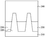
도 1은 일부 실시예에 따른 예시적인 반도체 디바이스의 사시도이다. 반도체 디바이스는 기판(110)을 포함한다. 일부 실시예에서, 기판(110)은 벌크 실리콘 기판을 포함한다. 일부 실시예에서, 기판(110)은 결정질 구조의 실리콘일 수 있다. 일부 다른 실시예에서, 기판(110)은 게르마늄과 같은 다른 원소 반도체를 포함할 수 있거나, 또는 실리콘 카바이드, 갈륨 비소화물, 인듐 비소화물, 또는 인듐 인화물과 같은 화합물 반도체를 포함할 수 있다. 또 다른 일부 실시예에서, 기판(110)은 SOI(silicon-on-insulator) 기판을 포함한다. SOI 기판은 SIMOX(separation by implantation of oxygen), 웨이퍼 본딩, 및/또는 기타 적합한 방법을 사용하여 제조될 수 있다.1 is a perspective view of an exemplary semiconductor device according to some embodiments. The semiconductor device includes a
반도체 디바이스는 반도체 핀(120)을 둘러싸는 쉘로우 트렌치 아이솔레이션(STI; shallow trench isolation) 구조물(130)을 더 포함한다. STI 구조물(130)은 실리콘 산화물과 같은 임의의 적합한 절연 재료를 포함할 수 있다. 일부 실시예에서, STI 구조물(130)은 예를 들어 약 30 nm 내지 약 60 nm 범위의 두께를 갖는다.The semiconductor device further includes a shallow trench isolation (STI)
반도체 디바이스(100)는 적어도 하나의 게이트 구조물(140)을 더 포함한다. 게이트 구조물(140)은 반도체 핀(120)의 일부 상에 형성된다. 게이트 구조물(140)은 게이트 유전체 층(141) 및 게이트 전극 층(142)을 포함한다. 게이트 유전체 층(141)은 게이트 전극 층(144)과 기판(110) 사이에 존재하고, 반도체 핀(120) 상에 형성된다. 전자 고갈을 막는 게이트 유전체 층(141)은 예를 들어, 금속 산화물, 금속 질화물, 금속 실리케이트, 전이 금속 산화물, 전이 금속 질화물, 전이 금속 실리케이트, 금속의 산질화물, 금속 알루미네이트, 지르코늄 실리케이트, 지르코늄 알루미네이트, 또는 이들의 조합과 같은 하이 k(high-k) 유전체 재료를 포함할 수 있다. 일부 실시예는 하프늄 산화물(HfO2), 하프늄 실리콘 산화물(HfSiO), 하프늄 실리콘 산질화물(HfSiON), 하프늄 탄탈 산화물(HfTaO), 하프늄 티타늄 산화물(HfTiO), 하프늄 지르코늄 산화물(HfZrO), 란탄 산화물(LaO), 지르코늄 산화물(ZrO), 티타늄 산화물(TiO), 탄탈 산화물(Ta2O5), 이트륨 산화물(Y2O3), 스트론튬 티타늄 산화물(SrTiO3, STO), 바륨 티타늄 산화물(BaTiO3, BTO), 바륨 지르코늄 산화물(BaZrO), 하프늄 란탄 산화물(HfLaO), 란탄 실리콘 산화물(LaSiO), 알루미늄 실리콘 산화물(AlSiO), 알루미늄 산화물(Al2O3), 실리콘 질화물(Si3N4), 산질화물(SiON), 및 이들의 조합을 포함할 수 있다. 게이트 유전체 층(141)은 실리콘 산화물(예컨대, 계면 층)의 하나의 층 및 하이 k 재료의 또다른 층과 같은 다층 구조물을 가질 수 있다.The semiconductor device 100 further includes at least one
게이트 전극 층(142)은 게이트 유전체 층(141) 및 게이트 유전체 층(141)에 의해 커버된 반도체 핀(120)의 부분을 커버하도록 기판(110) 위에 형성된다. 일부 실시예에서, 게이트 전극 층(142)은 폴리실리콘, 비정질 실리콘 등과 같은 반도체 재료를 포함한다. 게이트 전극 층(142)은 도핑 또는 미도핑 성막될 수 있다. 예를 들어, 일부 실시예에서, 게이트 전극 층(142)은 LPCVD(low-pressure chemical vapor deposition)에 의해 미도핑 성막된 폴리실리콘을 포함한다. 도포되면, 폴리실리콘은 반도체 디바이스의 타입에 기초하여 예를 들어 인 이온(또는 다른 n 타입 도펀트) 또는 붕소(또는 다른 p 타입 도펀트)로 도핑될 수 있다. 폴리실리콘은 또한, 예를 들어 인시추(in-situ) 도핑된 폴리실리콘의 퍼니스 성막(furnace deposition)에 의해 성막될 수 있다. 대안으로서, 게이트 전극 층(142)은 텅스텐(W), 니켈(Ni), 알루미늄(Al), 탄탈(Ta), 티타늄(Ti), 또는 이들의 임의의 조합과 같은 금속을 포함하는 폴리실리콘 금속 합금 또는 금속 게이트를 포함할 수 있다.A
반도체 핀(120)은 게이트 구조물(140)에 의해 커버되어 감싸진 채널 영역(도시되지 않음)을 포함한다. 반도체 핀(120)은 n 타입 finFET(NMOS 디바이스) 또는 p 타입 finFET(PMOS 디바이스)에 대해 적합한 채널을 제공하도록 도핑될 수 있다. 반도체 핀(120)은 이온 주입, 확산, 어닐링 및/또는 기타 적합한 프로세스와 같은 프로세스를 사용하여 도핑될 수 있다.The
반도체 디바이스는 스페이서 쌍(150)을 더 포함한다. 스페이서(150)는 각각 기판(110) 위에 그리고 게이트 구조물(140)의 대향 측부에 인접하게 형성된다. 반도체 핀(120)의 부분들은 스페이서(150)에 의해 커버된다. 일부 실시예에서, 스페이서(150)는 실리콘 산화물, 실리콘 질화물, 실리콘 산질화물, 또는 기타 적합한 재료를 포함할 수 있다. 스페이서(150)는 단일 층 또는 다층 구조물을 포함할 수 있다.The semiconductor device further includes a spacer pair (150).
도 1의 라인 2를 따라 취한 단면도인 도 2를 참조한다. 반도체 핀(120)은 스페이서(150) 사이에 적어도 하나의 리세스(121)를 포함한다. 리세스(121)는 스페이서(150) 및 게이트 구조물(140)에 의해 커버되지 않은 반도체 핀(120)의 부분 상에 형성된다. 보다 구체적으로, 게이트 구조물(140) 및 스페이서(150) 둘 다에 의해 노출된 반도체 핀(120)의 부분이 반도체 핀(120)에 리세스(121)를 형성하도록 부분적으로 제거된다(또는 부분적으로 리세스됨).2, which is a cross-sectional view taken along
반도체 디바이스(100)는 적어도 하나의 에피텍시 구조물(160)을 더 포함한다. 에피텍시 구조물(160)은 반도체 핀(120) 상에 형성된다. 보다 구체적으로, 에피텍시 구조물(160)은 반도체 핀(120)의 리세스(121)에 형성된다. 일부 실시예에서, 반도체 핀(120)은 최상부(topmost) 표면(122)을 갖는다. 에피텍시 구조물(160)은 최상부 표면(122) 아래로 기판(110)을 향해 연장한다. 일부 실시예에서, 복수의 에피텍시 구조물(160)이 각각 반도체 핀(120) 상에 에피텍셜 성장될 수 있다. 에피텍시 성장은 수직 성장 및 수평 성장을 포함하기 때문에, 반도체 핀(120)으로부터 성장된 하나의 에피텍시 구조물(160)의 일부는 이웃하는 반도체 핀(120)으로부터 성장된 에피텍시 구조물(160)의 일부와 결국 합쳐진다. 그리하여, 상이한 반도체 핀(120) 상에 형성된 에피텍시 구조물(160)이 연속 에피텍시 구조물로 합쳐질 수 있으며, 이는 그 위에 형성될 소스/드레인에 유용할 수 있다.The semiconductor device 100 further includes at least one
에피텍시 구조물(160)은 하나 이상의 에피텍시 또는 에피텍셜(에피) 프로세스를 사용함으로써 형성될 수 있으며, 그리하여 Si 특징부, SiGe 특징부, 및/또는 기타 적합한 특징부가 반도체 핀(120) 상에 결정질 상태로 형성될 수 있다. 일부 실시예에서, 에피텍시 구조물(160)의 격자 상수는 반도체 핀(120)의 채널의 격자 상수와 상이하며, 그리하여 반도체 디바이스의 캐리어 모빌리티를 개선하고 디바이스 성능을 향상시키도록 채널이 에피텍시 구조물(160)에 의해 변형 또는 스트레싱될 수 있다.The
반도체 디바이스(100)는 층간 유전체(ILD; interlayer dielectric) 층(180)을 더 포함한다. ILD 층(180)은 에피텍시 구조물(160)을 커버하도록 기판(110) 상에 형성된다. ILD 층(180)은 실리콘 산화물, 실리콘 질화물, 실리콘 산질화물, 실리콘 카바이드, 저유전상수 유전체 재료, 또는 이들의 조합을 포함할 수 있다.The semiconductor device 100 further includes an interlayer dielectric (ILD)
반도체 디바이스는 소스/드레인 컨택(190)을 더 포함한다. 소스/드레인 컨택(190)은 ILD 층(180)을 통해 형성되고, 에피텍시 구조물(160)의 상부 표면(169)과 접촉한다. 일부 실시예에서, 소스/드레인 컨택(!90)은 W, Co, Cu, Al 또는 기타 적합한 전도성 재료를 포함한다. 도 1에 도시된 바와 같이, 상이한 반도체 핀(120) 상에 형성된 에피텍시 구조물(160)이 연속 에피텍시 구조물로 합쳐질 때, 소스/드레인 컨택(190)은 이들 에피텍시 구조물(160) 상에 형성될 수 있다.The semiconductor device further includes a source / drain contact (190). A source /
일부 실시예에서, 에피텍시 구조물(160)은 게르마늄 함유 구조물이다. 예를 들어, 에피텍시 구조물(160)은 실리콘 게르마늄을 포함할 수 있다. 에피텍시 구조물(160)은 화학적 기상 증착(CVD; chemical vapor deposition)을 사용하여 형성될 수 있다. 전구체는 각각 SiH4 및 GeH4와 같은 실리콘 함유 가스 및 게르마늄 함유 가스를 포함할 수 있고, 실리콘 함유 가스 및 게르마늄 함유 가스의 부분 압력은 게르마늄 원자 퍼센티지 및 실리콘 원자 퍼센티지를 수정하도록 조정된다. 일부 실시예에서, 결과적인 에피텍시 구조물(160)은 최상부 부분(PT), 제1 부분(P1), 및 제2 부분(P2)을 포함한다. 상부 부분(PT), 제1 부분(P1), 및 제2 부분(P2)은 반도체 핀(120)으로부터 기판(110)으로의 방향을 따라 배열된다. 제1 부분(P1)은 최상부 부분(PT)의 게르마늄 원자 퍼센티지 및 제2 부분(P2)의 게르마늄 원자 퍼센티지보다 더 높은 게르마늄 원자 퍼센티지를 갖는다. 다르게 말하자면, 제1 부분(P1) 위의 최상부 부분(PT) 및 제1 부분(P1) 아래의 제2 부분(P2) 둘 다 제1 부분(P1)보다 적은 게르마늄을 함유하며, 이는 적합한 크기 및 형상의 상부 표면(169)을 갖도록 결과적인 에피텍시 구조물(160)에 유용할 수 있고 그 위에 형성된 소스/드레인 컨택(190)에 유용할 수 있다. 일부 실시예에서, SiH4와 같은 실리콘 함유 가스의 유량에 대한, GeH4와 같은 게르마늄 함유 가스의 유량의 비는, 에피텍시 구조물(160)의 에피텍시 성장 동안 최상부 부분(PT), 제1 부분(P1), 및 제2 부분(P2)의 전술한 게르마늄 원자 퍼센티지를 형성하도록 제어되거나 조정될 수 있다. 일부 실시예에서, 게르마늄 원자 퍼센티지는 게르마늄 농도로 지칭될 수 있다.In some embodiments, the
일부 실시예에서, 에피텍시 구조물(160)은 제1 부분(P1)과 제2 부분(P2) 사이의 중간 매립 층(161)을 포함한다. 중간 매립 층(161)의 게르마늄 원자 퍼센티지는 기판(110)으로부터 반도체 핀(120)으로의 방향을 따라 증가한다. 다르게 말하자면, 중간 매립 층(161)의 게르마늄 원자 퍼센티지는 제2 부분(P2)으로부터 제1 부분(P1)으로의 방향을 따라 증가한다. 이는 소스/드레인 컨택(109)의 형성에 유용하도록 적합한 크기 및 형상으로 형성될 에피텍시 구조물(160)의 상부 표면(169)에 유용할 수 있다. 일부 실시예에서, 중간 매립 층(161)은 게르마늄 원자 퍼센티지가 위쪽으로 점차 증가하여 구배되는 구배(gradient) 게르마늄 함유 층이다. 일부 실시예에서, 중간 매립 층(161)의 최하부 위치(즉, 제2 부분(P2))는 약 25% 내지 약 55% 범위의 게르마늄 원자 퍼센티지를 갖고, 최하부 위치 위의 중간 매립 층(161)의 다른 위치의 게르마늄 원자 퍼센티지는 위쪽으로 증가한다. 일부 실시예에서, SiH4와 같은 실리콘 함유 가스의 유량에 대한, GeH4와 같은 게르마늄 함유 가스의 유량의 비는, 중간 매립 층(161)의 에피텍시 성장 동안 중간 매립 층(161)의 전술한 구배 게르마늄 원자 퍼센티지를 형성하도록 제어되거나 조정될 수 있다.In some embodiments, the
일부 실시예에서, 에피텍시 구조물(160)은 상부 매립 층(162)을 더 포함한다. 상부 매립 층(162)은 중간 매립 층(161)과 최상부 부분(PT) 사이에 위치된다. 상부 매립 층(162)은 기판(110)으로부터 반도페 핀(120)으로의 방향을 따라 감소하는 게르마늄 원자 퍼센티지를 갖는다. 다르게 말하자면, 상부 매립 층(162)의 게르마늄 원자 퍼센티지는 제1 부분(P1)으로부터 최상부 부분(PT)으로의 방향을 따라 감소한다. 이는 중간 매립 층(161)보다 더 적은 게르마늄을 함유하는 최상부 부분(PT)의 형성에 유용할 수 있다. 일부 실시예에서, 상부 매립 층(162)은 게르마늄 원자 퍼센티지가 위쪽으로 점차 감소하여 구배되는 구배 게르마늄 함유 층이다. 일부 실시예에서, 상부 매립 층(162)의 최하부 위치(즉, 제1 부분(P1))는 약 45 % 내지 약 55% 범위의 게르마늄 원자 퍼센티지를 갖고, 최하부 위치 위의 상부 매립 층(162)의 다른 위치의 게르마늄 원자 퍼센티지는 위쪽으로 감소한다. 일부 실시예에서, SiH4와 같은 실리콘 함유 가스의 유량에 대한, GeH4와 같은 게르마늄 함유 가스의 유량의 비는, 상부 매립 층(162)의 에피텍시 성장 동안 상부 매립 층(162)의 전술한 구배 게르마늄 원자 퍼센티지를 형성하도록 제어되거나 조정될 수 있다.In some embodiments, the
일부 실시예에서, 에피텍시 구조물(160)은 최상부 층(163)을 더 포함한다. 최상부 부분(PT)은 아래의 상부 및 중간 매립 층(162 및 161)에 대향하는 최상부 층(163)의 최상부 표면 상에 위치된다. 다르게 말하자면, 상부 매립 층(162)은 최상부 층(163)과 중간 매립 층(161) 사이에 위치된다. 최상부 층(163)은 중간 매립 층(161)의 게르마늄 원자 퍼센티지보다 적은 게르마늄 원자 퍼센티지를 갖는다. 최상부 층(163)의 게르마늄 원자 퍼센티지는 기판(110)으로부터 반도체 핀(120)으로의 방향을 따라 적어도 부분적으로 감소한다. 구체적으로, 최상부 층(163)의 적어도 상부 부분의 게르마늄 원자 퍼센티지는 위쪽으로 감소하며, 이는 최상부 층(163)의 다른 아래의 위치보다 더 적은 게르마늄을 함유하는 최상부 부분(PT)의 형성에 유용할 수 있다. 일부 실시예에서, 최상부 층(163)의 게르마늄 원자 퍼센티지는 약 15% 내지 약 25% 범위이다. 일부 실시예에서, 최상부 층(163)의 최대 게르마늄 원자 퍼센티지는 상부 매립 층(162)의 최소 게르마늄 원자 퍼센티지와 최대 게르마늄 원자 퍼센티지 사이 범위이다. 다르게 말하자면, 상부 매립 층(162)에 바로 인접한 최상부 층(163)의 하부 부분은 최상부 층(163)의 최대 게르마늄 원자 퍼센티지에 도달하도록 기판(110)으로부터 반도체 핀(120)으로의 방향을 따라 증가하는 게르마늄 원자 퍼센티지를 가질 수 있는 반면에, 최상부 층(163)의 상부 부분의 게르마늄 원자 퍼센티지는 최상부 층(163)의 최소 게르마늄 원자 퍼센티지에 도달하도록 동일 방향을 따라 감소한다. 일부 실시예에서, SiH4와 같은 실리콘 함유 가스의 유량에 대한, GeH4와 같은 게르마늄 함유 가스의 유량의 비는, 최상부 층(163)의 에피텍시 성장 동안 최상부 층(163)의 전술한 게르마늄 원자 퍼센티지 프로파일을 형성하도록 제어되거나 조정될 수 있다.In some embodiments, the
일부 실시예에서, 에피텍시 구조물(160)은 하부 매립 층(164)을 더 포함한다. 하부 매립 층(164)은 제2 부분(P2) 아래에 있다. 제2 부분(P2)의 게르마늄 원자 퍼센티지는 하부 매립 층(164)의 최대 게르마늄 원자 퍼센티지와 최소 게르마늄 원자 퍼센티지 사이 범위이다. 이는 소스/드레인 컨택(109)의 형성에 유용하도록 적합한 크기 및 형상으로 형성될 에피텍시 구조물(160)의 상부 표면(169)에 유용할 수 있다. 다르게 말하자면, 하부 매립 층(164)의 게르마늄 원자 퍼센티지는 공간적으로 다양하고, 이의 최대 게르마늄 원자 퍼센티지는 제2 부분(P2)의 게르마늄 원자 퍼센티지보다 더 높으며, 하부 매립 층(164)의 최소 게르마늄 원자 퍼센티지는 제2 부분(P2)의 게르마늄 원자 퍼센티지보다 더 낮다. 일부 실시예에서, 하부 매립 층(164)의 게르마늄 원자 퍼센티지는 약 25% 내지 약 35% 범위이다. 일부 실시예에서, SiH4와 같은 실리콘 함유 가스의 유량에 대한, GeH4와 같은 게르마늄 함유 가스의 유량의 비는, 하부 매립 층(164)의 에피텍시 성장 동안 하부 매립 층(164)의 전술한 게르마늄 원자 퍼센티지 프로파일을 형성하도록 제어되거나 조정될 수 있다.In some embodiments, the
일부 실시예에서, 반도체 디바이스는 도핑 층(170)을 더 포함한다. 도핑 층(170)은 에피텍시 구조물(160) 아래에 있다. 다르게 말하자면, 도핑 층(170)은 에피텍시 구조물(160) 아래에 위치된다. 에피텍시 구조물(160)은 도핑 층(170) 상에 컨포멀하게(conformally) 형성된다. 도핑 층(170)은 리세스(121)의 표면을 통해 반도체 핀(120)으로 붕소와 같은 적합한 p 타입 불순물을 도핑함으로써 형성될 수 있다. 도핑 층(170)은 하부 매립 층(164) 아래에 있다. 도핑 층(170)은 기판(110)으로부터 반도페 핀(120)으로의 방향을 따라 증가하는 게르마늄 원자 퍼센티지를 갖는다. 다르게 말하자면, 도핑 층(170)의 게르마늄 원자 퍼센티지는 아래쪽으로 감소한다. 이는 소스/드레인 컨택(190)의 형성에 유용하도록 적합한 크기 및 형상으로 형성될 에피텍시 구조물(160)의 상부 표면(169)에 유용할 수 있다. 일부 실시예에서, SiH4와 같은 실리콘 함유 가스의 유량에 대한, GeH4와 같은 게르마늄 함유 가스의 유량의 비는, 도핑 층(170)의 형성 동안 도핑 층(170)의 전술한 게르마늄 원자 퍼센티지 프로파일을 형성하도록 제어되거나 조정될 수 있다.In some embodiments, the semiconductor device further comprises a
도 3은 일부 실시예에 따른 게르마늄 원자 퍼센티지 프로파일이다. 도 3에서, 프로파일 L1은 도핑 층(170)의 게르마늄 원자 퍼센티지 프로파일이고, 프로파일 L2는 하부 매립 층(164)의 게르마늄 원자 퍼센티지 프로파일이고, 프로파일 L3은 중간 매립 층(161)의 게르마늄 원자 퍼센티지 프로파일이고, 프로파일 L4는 상부 매립 층(162)의 게르마늄 원자 퍼센티지 프로파일이고, 프로파일 L5는 최상부 층(163)의 게르마늄 원자 퍼센티지 프로파일이다. 이러한 게르마늄 원자 퍼센티지 프로파일(L1-L5)을 갖는 이러한 에피텍시 구조물(160) 및 도핑 층(170)에 의해, 에피텍시 구조물(160)의 상부 표면(169)은 그 위에 형성된 소스/드레인 컨택(190)에 유용하도록 적합한 크기 및 형상으로 형성될 수 있다. 일부 실시예에서, SiH4와 같은 실리콘 함유 가스의 유량에 대한, GeH4와 같은 게르마늄 함유 가스의 유량의 비는, 에피텍시 구조물(160) 및 도핑 층(170)의 형성 동안 게르마늄 원자 퍼센티지 프로파일(L1-L5)을 형성하도록 제어되거나 조정될 수 있다.Figure 3 is a germanium atomic percentage profile according to some embodiments. In Figure 3, profile L1 is the germanium atomic percentage profile of the doped
에피텍시 구조물(160)은 반도체 디바이스의 소스 영역 또는 드레인 영역으로서의 역할을 하도록 적합한 불순물로 도핑된다. 일부 실시예에서, 에피텍시 구조물(160)은 붕소와 같은 p 타입 불순물로 도핑되고, 에피텍시 구조물(160)의 붕소 농도는 공간적으로 다양하다. 다르게 말하자면, 에피텍시 구조물(160)의 붕소 농도는 불균등하게 분포된다. 일부 실시예에서, p 타입 불순물의 농도는 주입 프로세스에 사용된 p 타입 도펀트의 주입량(dose)과 상관되고, 따라서 붕소 도펀트의 주입량은 에피텍시 구조물(160)의 공간적으로 다양한 붕소 농도를 형성하도록 제어되거나 조정될 수 있다. 붕소 도핑된 에피텍시 구조물(160)은 p 타입 소스/드레인 영역으로서 작용할 수 있다. 따라서, 반도체 디바이스는 p 타입 finFET으로서 작용할 수 있다.
일부 실시예에서, 에피텍시 구조물(160)의 붕소 농도는 도핑 층(170)으로부터 최상부 층(163)으로 실질적으로 증가한다. 다르게 말하자면, 도핑 층(170)의 붕소 농도는 하부 매립 층(164)의 붕소 농도보다 더 낮다. 하부 매립 층(164)의 붕소 농도는 중간 매립 층(161)의 붕소 농도보다 더 낮다. 중간 매립 층(161)의 붕소 농도는 상부 매립 층(162)의 붕소 농도보다 더 낮다. 상부 매립 층(162)의 붕소 농도는 최상부 층(163)의 붕소 농도보다 더 낮다. 일부 실시예에서, 도핑 층(170)의 붕소 농도는 기판(110)으로부터 반도체 핀(120)으로의 방향을 따라 왔다갔다한다(oscillate). 예를 들어, 일부 실시예에 따른 붕소 농도 프로파일인 도 4를 참조한다. 도 4에서, 프로파일 L6은 도핑 층(170)의 붕소 농도 프로파일이고, 프로파일 L7은 하부 매립 층(164)의 붕소 농도 프로파일이고, 프로파일 L8은 중간 매립 층(161)의 붕소 농도 프로파일이고, 프로파일 L9는 상부 매립 층(162)의 붕소 농도 프로파일이고, 프로파일 L10은 최상부 층(163)의 붕소 농도 프로파일이다. 이러한 붕소 농도 프로파일(L6-L10)을 갖는 붕소 도핑된 에피텍시 구조물(160) 및 붕소 도핑 층(170)에 의해, 에피텍시 구조물(160)의 상부 표면(169)은 그 위에 형성된 소스/드레인 컨택(190)에 유용하도록 적합한 크기 및 형상으로 형성될 수 있다. 주입 프로세스에 사용된 붕소 도펀트의 주입량은 붕소 농도 프로파일(L6 내지 L10)을 구현하도록 제어되거나 조정될 수 있다. 일부 실시예에서, 도핑 층(170)의 붕소 농도는 약 1e17 cm-3 내지 약 1e21 cm-3 범위이고, 하부 매립 층(164)의 붕소 농도는 약 3e20 cm-3 내지 약 5e20 cm-3 범위이고, 중간 매립 층(161)의 붕소 농도는 약 6e20 cm-3 내지 약 10e20 cm-3 범위이고, 상부 매립 층(162)의 붕소 농도는 약 6e20 cm-3 내지 약 10e20 cm-3 범위이고, 최상부 층(163)의 붕소 농도는 약 8e20 cm-3 내지 약 11e20 cm-3 범위이다.In some embodiments, the boron concentration of the
일부 실시예에서, 결과적인 붕소 도핑된 에피텍시 구조물(160)은 약 45 nm 내지 약 65 nm 범위의 깊이를 갖는다. 결과적인 붕소 도핑된 에피텍시 구조물(160)의 상부 표면(169)은 반도체 핀(120)의 최상부 표면(122)보다 더 높을 수 있고, 상부 표면(169)으로부터 최상부 표면(122)까지의 수직 거리는 5 nm일 수 있다. 다르게 말하자면, 에피텍시 구조물(160)의 일부는 리세스(121)의 초과부(excess)에 형성되며, 이는 소스/드레인 컨택(190)의 형성에 유용할 수 있다. 일부 실시예에서, 최상부 층(163)은 약 2.7 nm 내지 약 7.5 nm 범위의 두께를 가질 수 있고, 최상부 층(163)을 제외한 에피텍시 구조물(160)의 다른 부분의 최대 폭은 약 35 nm 내지 약 55 nm 범위일 수 있다. 이 최대 폭은 도 1에 도시된 바와 같이 에피텍시 구조물(160)의 배열 방향을 따라 측정된다.In some embodiments, the resulting boron doped
도 5a 내지 도 12a는, 도 1의 게이트 구조물(140)의 세로 방향에 평행한 라인과 같은 라인을 따라 취한, 일부 실시예에 따른 다양한 단계에서의 반도체 디바이스를 형성하는 방법의 단면도들이다. 도 5b 내지 도 12b는 도 1의 라인 2와 같은 라인을 따라 취한, 도 5a 내지 도 12a에 대응하는 상이한 단면도들이다.5A-12A are cross-sectional views of a method of forming a semiconductor device at various stages, according to some embodiments, taken along the same line as the line parallel to the longitudinal direction of the
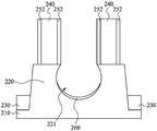
도 5a 및 도 5b를 참조한다. 반도체 핀(220)이 기판(210)에 형성되고, 반도체 핀(220)의 일부가 기판(210)으로부터 돌출된다. 반도체 핀(220)은 예를 들어 포토리소그래피 기술을 사용하여 기판(210)을 패터닝 및 에칭함으로써 형성될 수 있다. 일부 실시예에서, 포토레지스트 재료의 층(도시되지 않은)이 기판(210) 위에 성막된다. 포토레지스트 재료의 층은 원하는 패턴(이 경우에는 반도체 핀(220))에 따라 조사되고(노출되고) 포토레지스트 재료의 일부를 제거하도록 현상된다. 남아있는 포토레지스트 재료는 에칭과 같은 후속 프로세싱 단계로부터 아래의 재료를 보호한다. 산화물 또는 실리콘 질화물 마스크와 같은 다른 마스크도 또한 에칭 프로세스에 사용될 수 있다는 것을 유의하여야 한다.5A and 5B. A
도 5a 및 도 5b에서, 복수의 STI 구조물(230)이 기판(210) 상에 형성된다. STI 구조물(230)은 전구체로서 TEOS(tetra-ethyl-ortho-silicate) 및 산소를 사용하여 화학적 기상 증착(CVD; chemical vapor deposition)에 의해 형성될 수 있다. 일부 다른 실시예에서, STI 구조물(230)은 기판(210)으로 산소, 질소, 탄소 등과 같은 이온을 주입함으로써 형성될 수 있다. 또 일부 다른 실시예에서, STI 구조물(230)은 SOI 웨이퍼의 절연체 층이다.In FIGS. 5A and 5B, a plurality of
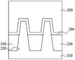
도 6a 및 도 6b를 참조한다. 더미 게이트 구조물(240)이 간격을 두고 반도체 핀(220)의 일부 상에 형성되며 반도체 핀(220)의 또다른 부분을 노출시킨다. 더미 게이트 구조물(240)은 폴리실리콘을 포함하고, 이들은 CVD 프로세스와 같은 성막 프로세스에 의해 형성될 수 있다.6A and 6B. A
도 7a 및 도 7b를 참조한다. 유전체 층(250)이 반도체 핀(220) 및 더미 게이트 구조물(240) 위에 컨포멀하게 형성된다. 일부 실시예에서, 유전체 층(250)은 실리콘 산화물, 실리콘 질화물, 실리콘 산질화물, 또는 기타 적합한 재료를 포함할 수 있다. 유전체 층(250)은 단일 층 또는 다층 구조물을 포함할 수 있다. 유전체 층(250)은 원자층 증착(ALD; atomic layer deposition) 프로세스, CVD 프로세스, PVD 프로세스 또는 스퍼터 성막 프로세스 또는 기타 적합한 기술과 같은 성막 프로세스에 의해 형성될 수 있다.7A and 7B. A
도 8a 및 도 8b를 참조한다. 반도체 핀(220)의 일부가 노출되도록 유전체 층(250)의 일부와 아래의 반도체 핀(220)의 일부를 제거하기 위한 제거 프로세스가 수행된다. 도 8b에 도시된 바와 같이, 이 제거 프로세스는 각각의 반도체 핀(220) 상에 노출된 리세스(221)를 형성할 수 있다. 도 8b에 도시된 바와 같이, 유전체 층(250)의 일부 남은 부분은 더미 게이트 구조물(240)의 2개의 대향 측부 상에 위치된 한 쌍의 스페이서(252)로서 작용한다. 일부 실시예에서, 스페이서(252)는 리세스(221)에 형성되는 후속 형성된 에피텍시 구조물을 오프셋시키는데 사용될 수 있다. 스페이서(252)는 에피텍시 구조물의 프로파일을 설계하거나 수정하기 위해 더 사용될 수 있다.8A and 8B. A removal process is performed to remove a portion of the
제거 프로세스는 건식 에칭 프로세스, 습식 에칭 프로세스, 또는 건식 및 습식 에칭 프로세스의 조합일 수 있다. 제거는 에칭 프로세스를 용이하게 하도록 리소그래피 프로세스를 포함할 수 있다. 리소그래피 프로세스는 포토레지스트 코팅(예컨대, 스핀온 코팅), 소프트 베이킹, 마스크 정렬, 노광, 노광-후 베이킹, 포토레지스트 현상, 린싱, 건조(예컨대, 하드 베이킹), 기타 적합한 프로세스, 또는 이들의 조합을 포함할 수 있다. 대안으로서, 리소그래피 프로세스는 마스크리스 포토리소그래피, 전자빔 기록 및 이온빔 기록과 같은 다른 방법에 의해 구현되거나 교체된다. 또 일부 다른 실시예에서, 리소그래피 프로세스는 나노임프린트 기술을 구현할 수 있다. 일부 실시예에서, 리세스(221)를 HF 또는 기타 적합한 용액으로 세척하는 예비세척이 수행될 수 있으며, 이는 후속 에피텍시 성장에 유용할 수 있다.The removal process may be a dry etch process, a wet etch process, or a combination of a dry and wet etch process. Removal may include a lithographic process to facilitate the etching process. The lithographic process may be performed by any suitable process known in the art, including but not limited to photoresist coating (e.g., spin-on coating), soft bake, mask alignment, exposure, post-exposure baking, photoresist development, rinsing, drying . Alternatively, the lithographic process is implemented or replaced by other methods such as maskless photolithography, electron beam recording, and ion beam recording. In still other embodiments, the lithographic process can implement nanoimprint techniques. In some embodiments, a prewash that cleans the
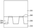
도 9a 및 도 9b를 참조한다. 도핑 층(260)이 반도체 핀(220)의 리세스(221)에 형성된다. 도핑 층(260)은 붕소와 같은 적합한 p 타입 불순물로 도핑된다. 예를 들어, 도핑 층(260)은 리세스(221)의 노출된 표면을 통해 반도체 핀(220)으로 붕소를 도핑함으로써 형성될 수 있다. 도핑 층(260)은 인시추(in-situ) 도핑 프로세스에 의해 형성될 수 있다. 도핑 프로세스는 노출된 표면을 통해 반도체 핀(220)으로 붕소와 같은 p 타입 불순물을 주입하는 주입 프로세스를 포함할 수 있다. 도핑 층(260)은 도 4에 도시된 바와 같은 게르마늄 원자 퍼센티지 프로파일(L1)을 가질 수 있다. 이 게르마늄 원자 퍼센티지 프로파일은, 예를 들어 SiH4와 같은 실리콘 함유 가스의 유량에 대한, GeH4와 같은 게르마늄 함유 가스의 유량의 비를 제어함으로써 달성될 수 있다. 도핑 층(260)은 도 5에 도시된 바와 같은 붕소 농도 프로파일(L6)을 가질 수 있다. 이 붕소 농도 프로파일은, 예를 들어 주입 프로세스에 사용된 붕소 도펀트의 주입량을 제어함으로써 달성될 수 있다.9A and 9B. A
도 10a 및 도 10b를 참조한다. 복수의 에피텍시 구조물(270)이 각각 반도체 핀(220)의 리세스(221)에 그리고 도핑 층(260) 위에 형성된다. 에피텍시 구조물(270)은 하나 이상의 에피텍시 또는 에피텍셜(에피) 프로세스를 사용하여 형성될 수 있으며, 그리하여 Si 특징부, SiGe 특징부, 및/또는 기타 적합한 특징부가 반도체 핀(220) 상에 결정질 상태로 형성될 수 있다. 일부 실시예에서, 에피텍시 프로세스는 CVD 성막 기술(예컨대, 기상 에피텍시(VPE; vapor-phase epitaxy) 및/또는 초고진공 CVD(UHV-CVD; ultra-high vacuum CVD), 분자 빔 에피텍시, 및/또는 기타 적합한 프로세스를 포함한다. 에피텍시 프로세스는 반도체 핀(220)의 조성물(예컨대, 실리콘)과 상호작용하는 기상 및/또는 액상 전구체를 사용할 수 있다.10A and 10B. A plurality of
에피텍시 구조물(270)은 게르마늄 함유 구조물이다. 예를 들어, 에피텍시 구조물(270)은 실리콘 게르마늄을 포함할 수 있다. 에피텍시 구조물(270)은 화학적 기상 증착(CVD)을 사용하여 형성될 수 있다. 전구체는 각각 SiH4 및 GeH4와 같은 실리콘 함유 가스 및 게르마늄 함유 가스를 포함할 수 있고, 실리콘 함유 가스 및 게르마늄 함유 가스의 부분 압력은 게르마늄 원자 퍼센티지 및 실리콘 원자 퍼센티지를 수정하도록 조정된다. 구체적으로, SiH4와 같은 실리콘 함유 가스의 유량에 대한, GeH4와 같은 게르마늄 함유 가스의 유량의 비는, 에피텍시 구조물(270)의 에피텍시 성장 동안 도 4에 도시된 바와 같은 게르마늄 원자 퍼센티지 프로파일(L2-L5)을 형성하도록 제어되거나 조정될 수 있다. 에피텍셜 성장은 수직 성장 및 수평 성장을 포함하기 때문에, 일부 실시예에서, 반도체 핀(220)으로부터 성장된 하나의 에피텍시 구조물(270)의 일부는 이웃하는 반도체 핀(220)으로부터 성장된 에피텍시 구조물(270)의 일부와 결국 합쳐진다. 그리하여, 상이한 반도체 핀(220) 상에 형성된 에피텍시 구조물(270)이 연속 에피텍시 구조물로 합쳐질 수 있으며, 이는 그 위에 형성될 소스/드레인 컨택에 유용할 수 있다.The
반도체 디바이스의 소스 영역 또는 드레인 영역으로서 작용하도록 에피텍시 구조물(270)로 적합한 불순물을 도핑하기 위한 도핑 프로세스가 수행된다. 예를 들어, 에피텍시 구조물(270)은 인시추 도핑될 수 있다. 도핑 종은 BF2와 같은 p 타입 도펀트, 인이나 비소와 같은 n 타입 도펀트, 및/또는 이들의 조합을 포함한 기타 적합한 도펀트를 포함한다. 에피텍시 구조물(270)이 인시추 도핑되지 않는 경우, 에피텍시 구조물(270)을 도핑하도록 제2 주입 프로세스(즉, 접합 주입 프로세스)가 수행된다. 주입은 에피텍시 구조물(270)로 도펀트를 주입하도록 수행될 수 있다. 에피텍시 구조물(270)을 활성화하도록 하나 이상의 어닐링 프로세스가 수행될 수 있다. 어닐링 프로세스는 급속 열 어닐링(RTA; rapid thermal annealing) 및/또는 레이저 어닐링 프로세스를 포함한다.A doping process is performed to dope suitable
일부 실시예에서, 도핑 프로세스는, 결과적인 에피텍시 구조물(270)의 붕소 농도가 공간적으로 다양하거나 불균등하게 분포되도록 에피텍시 구조물(270)로 붕소 도펀트를 불균등하게 도핑하도록 수행된다. 구체적으로, 에피텍시 구조물(270)은 도 5에 도시된 바와 같은 붕소 농도 프로파일(L7-10)을 가질 수 있다. 예를 들어, 에피텍시 구조물(270)에 수행된 주입 프로세스 동안 도 5에 도시된 바와 같은 붕소 농도 프로파일(L7-10)을 형성하도록 붕소 도펀트의 주입량이 제어되거나 조정될 수 있다. 이는 그 위에 형성되는 소스/드레인 컨택에 유용하도록 적합한 크기 및 형상으로 형성된 에피텍시 구조물(270)의 상부 표면(271)에 유용할 수 있다.In some embodiments, the doping process is performed to unevenly dope the boron dopant into the
도 11a 및 도 11b를 참조한다. 더미 게이트 구조물(240)을 게이트 구조물(280)로 교체하는 게이트 라스트(gate last) 프로세스(또는 교체 게이트 프로세스)가 수행된다. 게이트 구조물(280)은 게이트 유전체 층(281) 및 게이트 전극 층(282)을 포함할 수 있다. 게이트 전극 층(282)은 일함수 금속을 포함할 수 있다. 프로세스에서 게이트 구조물(280)을 나중에 제공하는 것은, 소스/드레인 에피텍시 구조물(270)의 형성 동안 일함수 금속의 안정성 문제를 피할 수 있다. 게이트 라스트 프로세스는, 에칭 프로세스에 의해 더미 게이트 구조물(240)을 제거하고, 성막 프로세스에 의해 게이트 유전체 층(281)을 형성하고, 성막 프로세스에 의해 게이트 전극 층(282)을 형성하고, 성막 프로세스에 의해 게이트 전극 층(282) 상에 유전체 캡핑 층을 형성하고, CMP 프로세스에 의해 유전체 캡핑 층의 원치않는 부분을 제거하는 것을 포함할 수 있다.11A and 11B. A gate last process (or alternate gate process) is performed to replace the
더미 게이트 구조물(240)을 제거하기 전에, 층간 유전체(ILD; interlayer dielectric) 층(290)이 에피텍시 구조물(270) 위에 형성된다. ILD 층(290)은 실리콘 산화물, 실리콘 질화물, 실리콘 산질화물, 실리콘 카바이드, 저유전상수의 유전체 재료 또는 이들의 조합을 포함한다. ILD 층(290)은 CVD 프로세스와 같은 성막 프로세스에 의해 형성될 수 있다.Prior to removing the
도 12a 및 도 12b를 참조한다. 소스/드레인 컨택(300)이 ILD 층(290)을 통해 형성되고, 에피텍시 구조물(270)의 상부 표면(271)과 접촉한다. 소스/드레인 컨택(300)의 형성은, ILD 층(290)을 통해 아래로 에피텍시 구조물(270)까지 에칭하는 에칭 프로세스에 의해 컨택 홀을 형성하고, 소스/드레인 컨택(300)을 형성하도록 CVD 프로세스와 같은 성막 프로세스에 의해 컨택 홀에 금속을 성막하는 것을 포함할 수 있다.12A and 12B. A source /
일부 실시예에서, 게르마늄 원자 퍼센티지 프로파일 및 p 타입 불순물 농도 프로파일이 적합한 크기 및 형상으로 형성된 에피텍시 구조물의 상부 표면을 이루므로, 소스/드레인 컨택이 보다 용이하게 상부 표면 상에 형성될 수 있고, 컨택 저항도 감소될 수 있다.In some embodiments, the germanium atomic percentage profile and the p-type impurity concentration profile make up the top surface of the epitaxial structure formed into a suitable size and shape, so that the source / drain contact can be more easily formed on the top surface, Contact resistance can also be reduced.
일부 실시예에 따르면, 반도체 디바이스는 기판, 적어도 하나의 반도체 핀, 및 적어도 하나의 에피텍시 구조물을 포함한다. 반도체 핀은 기판 상에 존재한다. 반도체 핀은 위에 적어도 하나의 리세스가 구비된다. 에피텍시 구조물은 반도체 핀의 리세스에 존재한다. 에피텍시 구조물은 반도체 핀으로부터 기판으로의 방향을 따라 배열된 최상부 부분, 제1 부분 및 제2 부분을 포함한다. 제1 부분은 최상부 부분의 게르마늄 원자 퍼센티지 및 제2 부분의 게르마늄 원자 퍼센티지보다 더 높은 게르마늄 원자 퍼센티지를 갖는다.According to some embodiments, a semiconductor device includes a substrate, at least one semiconductor fin, and at least one epitaxial structure. Semiconductor fins are present on the substrate. The semiconductor fin is provided with at least one recess thereon. The epitaxial structure is present in the recess of the semiconductor fin. The epitaxial structure includes a top portion, a first portion and a second portion arranged along a direction from the semiconductor fin to the substrate. The first portion has a germanium atomic percentage of the uppermost portion and a germanium atomic percentage higher than the germanium atomic percentage of the second portion.
일부 실시예에 따르면, 반도체 디바이스는 기판, 적어도 하나의 반도체 핀, 및 적어도 하나의 에피텍시 구조물을 포함한다. 반도체 핀은 위에 적어도 하나의 리세스가 구비된다. 에피텍시 구조물은 반도체 핀의 리세스에 존재한다. 에피텍시 구조물은 최상부 층 및 상기 최상부 층 아래의 제1 구배 게르마늄 함유 층을 포함한다. 제1 구배 게르마늄 함유 층은, 최상부 층의 게르마늄 원자 퍼센티지보다 더 높으며 기판으로부터 반도체 핀으로의 방향을 따라 증가하는 게르마늄 원자 퍼센티지를 갖는다.According to some embodiments, a semiconductor device includes a substrate, at least one semiconductor fin, and at least one epitaxial structure. The semiconductor fin is provided with at least one recess thereon. The epitaxial structure is present in the recess of the semiconductor fin. The epitaxial structure comprises a top layer and a first-order germanium-containing layer below the top layer. The first-order germanium-containing layer is higher than the germanium atomic percentage of the topmost layer and has a germanium atomic percentage that increases along the direction from the substrate to the semiconductor fin.
일부 실시예에 따르면, 반도체 디바이스의 형성 방법은, 기판 상에 적어도 하나의 반도체 핀을 형성하는 단계, 적어도 하나의 리세스를 형성하도록 반도체 핀의 적어도 하나의 부분을 제거하는 단계, 및 반도체 핀의 리세스에 적어도 하나의 에피텍시 구조물을 형성하는 단계를 포함하고, 에피텍시 구조물은 반도체 핀으로부터 기판으로의 방향을 따라 배열된 최상부 부분, 제1 부분 및 제2 부분을 포함하며, 제1 부분의 게르마늄 농도는 최상부 부분의 게르마늄 농도 및 제2 부분의 게르마늄 농도보다 더 높다.According to some embodiments, a method of forming a semiconductor device includes forming at least one semiconductor fin on a substrate, removing at least one portion of the semiconductor fin to form at least one recess, Wherein the epitaxial structure comprises a top portion, a first portion and a second portion arranged along a direction from the semiconductor fin to the substrate, wherein the first portion and the second portion are arranged in a direction from the semiconductor fin to the substrate, The germanium concentration of the portion is higher than the germanium concentration of the uppermost portion and the germanium concentration of the second portion.
전술한 바는 당해 기술 분야에서의 숙련자들이 본 개시의 양상을 보다 잘 이해할 수 있도록 여러 실시예들의 특징을 나타낸 것이다. 당해 기술 분야에서의 숙련자라면, 여기에서 소개된 실시예와 동일한 목적을 수행하고/하거나 동일한 이점을 달성하기 위해 다른 프로세스 및 구조를 설계 또는 수정하기 위한 기반으로서 본 개시를 용이하게 사용할 수 있다는 것을 알아야 한다. 당해 기술 분야에서의 숙련자는 또한, 이러한 등가의 구성이 본 개시의 진정한 의미 및 범위로부터 벗어나지 않으며, 본 개시의 진정한 의미 및 범위에서 벗어나지 않고서 다양한 변경, 치환 및 대안을 행할 수 있다는 것을 알아야 한다.The foregoing presents features of various embodiments in order that those skilled in the art may better understand the aspects of the disclosure. It should be understood by those skilled in the art that the present disclosure can readily be used as a basis for designing or modifying other processes and structures to accomplish the same purposes and / or to achieve the same advantages as the embodiments disclosed herein do. Those skilled in the art will also appreciate that such equivalent constructions do not depart from the true spirit and scope of this disclosure, and that various changes, substitutions and alternatives may be made without departing from the true spirit and scope of this disclosure.
Claims (10)
Translated fromKorean기판;
상기 기판 상에 존재하는 적어도 하나의 반도체 핀으로서, 위에 적어도 하나의 리세스가 구비되는, 상기 적어도 하나의 반도체 핀; 및
상기 반도체 핀의 리세스에 존재하는 적어도 하나의 에피텍시 구조물을 포함하고,
상기 에피텍시 구조물은, 상기 반도체 핀으로부터 상기 기판으로의 방향을 따라 배열된 최상부(topmost) 부분, 제1 부분 및 제2 부분을 포함하고, 상기 제1 부분은 상기 최상부 부분의 게르마늄 원자 퍼센티지 및 상기 제2 부분의 게르마늄 원자 퍼센티지보다 더 높은 게르마늄 원자 퍼센티지를 갖는 것인 반도체 디바이스.A semiconductor device comprising:
Board;
At least one semiconductor fin on said substrate, said at least one semiconductor fin having at least one recess on said substrate; And
At least one epitaxial structure present in the recess of the semiconductor fin,
Wherein the epitaxial structure comprises a topmost portion, a first portion and a second portion arranged in a direction from the semiconductor fin to the substrate, the first portion comprising a germanium atomic percentage and a germanium atomic percentage of the topmost portion, And has a germanium atomic percentage higher than the germanium atomic percentage of the second portion.
기판;
상기 기판 상에 존재하는 적어도 하나의 반도체 핀으로서, 위에 적어도 하나의 리세스가 구비되는, 상기 적어도 하나의 반도체 핀; 및
상기 반도체 핀의 리세스에 존재하는 적어도 하나의 에피텍시 구조물을 포함하고,
상기 에피텍시 구조물은 최상부 층 및 상기 최상부 층 아래의 제1 구배(gradient) 게르마늄 함유 층을 포함하며, 상기 제1 구배 게르마늄 함유 층은, 상기 최상부 층의 게르마늄 원자 퍼센티지보다 더 높으며 상기 기판으로부터 상기 반도체 핀으로의 방향을 따라 증가하는 게르마늄 원자 퍼센티지를 갖는 것인 반도체 디바이스.A semiconductor device comprising:
Board;
At least one semiconductor fin on said substrate, said at least one semiconductor fin having at least one recess on said substrate; And
At least one epitaxial structure present in the recess of the semiconductor fin,
Wherein the epitaxial structure comprises a top layer and a first germanium containing layer below the top layer wherein the first layer of germanium containing germanium is higher than the germanium atomic percentage of the top layer and comprises And has a germanium atomic percentage increasing along a direction toward the semiconductor fin.
기판 상에 적어도 하나의 반도체 핀을 형성하는 단계;
적어도 하나의 리세스를 형성하도록 상기 반도체 핀의 적어도 하나의 부분을 제거하는 단계; 및
상기 반도체 핀의 리세스에 적어도 하나의 에피텍시 구조물을 형성하는 단계를 포함하고,
상기 에피텍시 구조물은 상기 반도체 핀으로부터 상기 기판으로의 방향을 따라 배열된 최상부 부분, 제1 부분 및 제2 부분을 포함하며, 상기 제1 부분의 게르마늄 농도는 상기 최상부 부분의 게르마늄 농도 및 상기 제2 부분의 게르마늄 농도보다 더 높은 것인 반도체 디바이스의 형성 방법.
A method of forming a semiconductor device,
Forming at least one semiconductor fin on the substrate;
Removing at least one portion of the semiconductor fin to form at least one recess; And
Forming at least one epitaxial structure in the recess of the semiconductor fin,
Wherein the epitaxial structure comprises a top portion, a first portion and a second portion arranged along a direction from the semiconductor fin to the substrate, the germanium concentration of the first portion being greater than the germanium concentration of the top portion and the germanium concentration of the first portion Lt; RTI ID = 0.0 > germanium < / RTI > concentration of the two portions.
Applications Claiming Priority (4)
| Application Number | Priority Date | Filing Date | Title |
|---|---|---|---|
| US201562218901P | 2015-09-15 | 2015-09-15 | |
| US62/218,901 | 2015-09-15 | ||
| US15/164,824 | 2016-05-25 | ||
| US15/164,824US10032873B2 (en) | 2015-09-15 | 2016-05-25 | Semiconductor device and method of forming the same |
Publications (2)
| Publication Number | Publication Date |
|---|---|
| KR20170032840Atrue KR20170032840A (en) | 2017-03-23 |
| KR101879042B1 KR101879042B1 (en) | 2018-07-16 |
Family
ID=58257540
Family Applications (1)
| Application Number | Title | Priority Date | Filing Date |
|---|---|---|---|
| KR1020160109935AActiveKR101879042B1 (en) | 2015-09-15 | 2016-08-29 | Semiconductor device and method of forming the same |
Country Status (4)
| Country | Link |
|---|---|
| US (4) | US10032873B2 (en) |
| KR (1) | KR101879042B1 (en) |
| CN (1) | CN106847916B (en) |
| TW (1) | TWI603477B (en) |
Cited By (6)
| Publication number | Priority date | Publication date | Assignee | Title |
|---|---|---|---|---|
| KR20200036733A (en)* | 2018-09-27 | 2020-04-07 | 타이완 세미콘덕터 매뉴팩쳐링 컴퍼니 리미티드 | Semiconductor device and methods of forming same |
| KR20200086607A (en)* | 2019-01-08 | 2020-07-17 | 삼성전자주식회사 | Semiconductor devices |
| KR20210011834A (en)* | 2019-07-23 | 2021-02-02 | 삼성전자주식회사 | Semiconductor device |
| KR20220029359A (en)* | 2020-08-31 | 2022-03-08 | 타이완 세미콘덕터 매뉴팩쳐링 컴퍼니 리미티드 | Epitaxial features |
| US12132113B2 (en) | 2019-01-08 | 2024-10-29 | Samsung Electronics Co., Ltd. | Multi-bridge channel transistors with stacked source/drain structure and method of forming the same |
| US12446254B2 (en) | 2024-02-13 | 2025-10-14 | Taiwan Semiconductor Manufacturing Company, Ltd. | Semiconductor device and methods of forming same |
Families Citing this family (20)
| Publication number | Priority date | Publication date | Assignee | Title |
|---|---|---|---|---|
| US9691898B2 (en)* | 2013-12-19 | 2017-06-27 | Taiwan Semiconductor Manufacturing Co., Ltd. | Germanium profile for channel strain |
| DE102016113434B4 (en)* | 2015-09-15 | 2020-11-19 | Taiwan Semiconductor Manufacturing Company, Ltd. | Semiconductor device and method of forming the same |
| US11152251B2 (en) | 2017-07-31 | 2021-10-19 | Taiwan Semiconductor Manufacturing Co., Ltd. | Method for manufacturing semiconductor device having via formed by ion beam |
| KR102385567B1 (en)* | 2017-08-29 | 2022-04-12 | 삼성전자주식회사 | Semiconductor devices and method of manufacturing semiconductor devices |
| CN111033756A (en) | 2017-09-29 | 2020-04-17 | 英特尔公司 | Apparatus, method and system for providing a stressed channel of a transistor |
| KR102606237B1 (en)* | 2018-02-09 | 2023-11-24 | 삼성전자주식회사 | integrated circuit semiconductor device including MOS(metal oxide semiconductor) transistor |
| US10763363B2 (en)* | 2018-04-10 | 2020-09-01 | Taiwan Semiconductor Manufacturing Co., Ltd. | Gradient doped region of recessed fin forming a FinFET device |
| US10840355B2 (en)* | 2018-05-01 | 2020-11-17 | Taiwan Semiconductor Manufacturing Company, Ltd. | Increasing source/drain dopant concentration to reduced resistance |
| US11227918B2 (en)* | 2018-07-31 | 2022-01-18 | Taiwan Semiconductor Manufacturing Company, Ltd. | Melt anneal source and drain regions |
| US11264237B2 (en)* | 2018-09-28 | 2022-03-01 | Taiwan Semiconductor Manufacturing Company, Ltd. | Method of epitaxy and semiconductor device |
| US10867861B2 (en)* | 2018-09-28 | 2020-12-15 | Taiwan Semiconductor Manufacturing Company, Ltd. | Fin field-effect transistor device and method of forming the same |
| US11257928B2 (en) | 2018-11-27 | 2022-02-22 | Taiwan Semiconductor Manufacturing Company, Ltd. | Method for epitaxial growth and device |
| US11621325B2 (en) | 2019-03-28 | 2023-04-04 | Intel Corporation | Source or drain structures with low resistivity |
| CN113611736B (en)* | 2020-05-29 | 2022-11-22 | 联芯集成电路制造(厦门)有限公司 | Semiconductor element and manufacturing method thereof |
| US11923436B2 (en)* | 2020-08-07 | 2024-03-05 | Taiwan Semiconductor Manufacturing Co., Ltd. | Source/drain structure for semiconductor device |
| US12068322B2 (en)* | 2021-01-29 | 2024-08-20 | Taiwan Semiconductor Manufacturing Co., Ltd. | Method of forming a multi-layer epitaxial source/drain region having varying concentrations of boron and germanium therein |
| US11990511B2 (en) | 2021-08-27 | 2024-05-21 | Taiwan Semiconductor Manufacturing Co., Ltd. | Source/drain device and method of forming thereof |
| KR102845855B1 (en)* | 2021-09-28 | 2025-08-14 | 삼성전자주식회사 | Semiconductor device and method for manufacturing the same |
| CN116504828A (en)* | 2022-01-19 | 2023-07-28 | 联华电子股份有限公司 | semiconductor element |
| US20240055485A1 (en)* | 2022-08-12 | 2024-02-15 | Taiwan Semiconductor Manufacturing Company, Ltd. | Semiconductor device and methods of fabrication thereof |
Citations (4)
| Publication number | Priority date | Publication date | Assignee | Title |
|---|---|---|---|---|
| US6943116B2 (en)* | 2002-02-22 | 2005-09-13 | Infineon Technologies Ag | Method for fabricating a p-channel field-effect transistor on a semiconductor substrate |
| US20130280875A1 (en)* | 2011-06-15 | 2013-10-24 | Taiwan Semiconductor Manufacturing Company, Ltd. | Method of manufacturing strained source/drain structures |
| KR20140111575A (en)* | 2013-03-11 | 2014-09-19 | 타이완 세미콘덕터 매뉴팩쳐링 컴퍼니 리미티드 | Finfet with rounded source/drain profile |
| KR20160011742A (en)* | 2014-07-22 | 2016-02-02 | 삼성전자주식회사 | Semiconductor device |
Family Cites Families (40)
| Publication number | Priority date | Publication date | Assignee | Title |
|---|---|---|---|---|
| JP3634830B2 (en)* | 2002-09-25 | 2005-03-30 | 株式会社東芝 | Power semiconductor device |
| US20060091490A1 (en)* | 2004-11-03 | 2006-05-04 | Hung-Wei Chen | Self-aligned gated p-i-n diode for ultra-fast switching |
| US7312128B2 (en)* | 2004-12-01 | 2007-12-25 | Applied Materials, Inc. | Selective epitaxy process with alternating gas supply |
| US8017487B2 (en)* | 2006-04-05 | 2011-09-13 | Globalfoundries Singapore Pte. Ltd. | Method to control source/drain stressor profiles for stress engineering |
| US7538387B2 (en)* | 2006-12-29 | 2009-05-26 | Taiwan Semiconductor Manufacturing Company, Ltd. | Stack SiGe for short channel improvement |
| JP5141029B2 (en)* | 2007-02-07 | 2013-02-13 | 富士通セミコンダクター株式会社 | Semiconductor device and manufacturing method thereof |
| US7667271B2 (en) | 2007-04-27 | 2010-02-23 | Taiwan Semiconductor Manufacturing Company, Ltd. | Fin field-effect transistors |
| KR101264113B1 (en)* | 2007-07-16 | 2013-05-13 | 삼성전자주식회사 | CMOS device having strained channel and method of fabricating the same |
| US7973372B2 (en)* | 2009-03-27 | 2011-07-05 | National Semiconductor Corporation | Semiconductor structure in which source and drain extensions of field-effect transistor are defined with different dopants |
| US8497528B2 (en) | 2010-05-06 | 2013-07-30 | Taiwan Semiconductor Manufacturing Company, Ltd. | Method for fabricating a strained structure |
| US8440517B2 (en) | 2010-10-13 | 2013-05-14 | Taiwan Semiconductor Manufacturing Company, Ltd. | FinFET and method of fabricating the same |
| US9245805B2 (en) | 2009-09-24 | 2016-01-26 | Taiwan Semiconductor Manufacturing Company, Ltd. | Germanium FinFETs with metal gates and stressors |
| US8362575B2 (en) | 2009-09-29 | 2013-01-29 | Taiwan Semiconductor Manufacturing Company, Ltd. | Controlling the shape of source/drain regions in FinFETs |
| US8610240B2 (en) | 2009-10-16 | 2013-12-17 | Taiwan Semiconductor Manufacturing Company, Ltd. | Integrated circuit with multi recessed shallow trench isolation |
| US8729627B2 (en) | 2010-05-14 | 2014-05-20 | Taiwan Semiconductor Manufacturing Company, Ltd. | Strained channel integrated circuit devices |
| US8796759B2 (en) | 2010-07-15 | 2014-08-05 | Taiwan Semiconductor Manufacturing Company, Ltd. | Fin-like field effect transistor (FinFET) device and method of manufacturing same |
| US8367498B2 (en) | 2010-10-18 | 2013-02-05 | Taiwan Semiconductor Manufacturing Company, Ltd. | Fin-like field effect transistor (FinFET) device and method of manufacturing same |
| US8962400B2 (en) | 2011-07-07 | 2015-02-24 | Taiwan Semiconductor Manufacturing Company, Ltd. | In-situ doping of arsenic for source and drain epitaxy |
| US8841701B2 (en) | 2011-08-30 | 2014-09-23 | Taiwan Semiconductor Manufacturing Company, Ltd. | FinFET device having a channel defined in a diamond-like shape semiconductor structure |
| US8723272B2 (en) | 2011-10-04 | 2014-05-13 | Taiwan Semiconductor Manufacturing Company, Ltd. | FinFET device and method of manufacturing same |
| US8723236B2 (en) | 2011-10-13 | 2014-05-13 | Taiwan Semiconductor Manufacturing Company, Ltd. | FinFET device and method of manufacturing same |
| US8603891B2 (en)* | 2012-01-20 | 2013-12-10 | Micron Technology, Inc. | Methods for forming vertical memory devices and apparatuses |
| US9171925B2 (en) | 2012-01-24 | 2015-10-27 | Taiwan Semiconductor Manufacturing Company, Ltd. | Multi-gate devices with replaced-channels and methods for forming the same |
| US8847293B2 (en) | 2012-03-02 | 2014-09-30 | Taiwan Semiconductor Manufacturing Company, Ltd. | Gate structure for semiconductor device |
| US8836016B2 (en) | 2012-03-08 | 2014-09-16 | Taiwan Semiconductor Manufacturing Company, Ltd. | Semiconductor structures and methods with high mobility and high energy bandgap materials |
| US8785285B2 (en) | 2012-03-08 | 2014-07-22 | Taiwan Semiconductor Manufacturing Company, Ltd. | Semiconductor devices and methods of manufacture thereof |
| US8680576B2 (en) | 2012-05-16 | 2014-03-25 | Taiwan Semiconductor Manufacturing Company, Ltd. | CMOS device and method of forming the same |
| US8729634B2 (en) | 2012-06-15 | 2014-05-20 | Taiwan Semiconductor Manufacturing Company, Ltd. | FinFET with high mobility and strain channel |
| KR20140042460A (en)* | 2012-09-28 | 2014-04-07 | 삼성전자주식회사 | Semiconductor device |
| US8809139B2 (en) | 2012-11-29 | 2014-08-19 | Taiwan Semiconductor Manufacturing Company, Ltd. | Fin-last FinFET and methods of forming same |
| US8853025B2 (en) | 2013-02-08 | 2014-10-07 | Taiwan Semiconductor Manufacturing Company, Ltd. | FinFET/tri-gate channel doping for multiple threshold voltage tuning |
| US9093514B2 (en) | 2013-03-06 | 2015-07-28 | Taiwan Semiconductor Manufacturing Co., Ltd. | Strained and uniform doping technique for FINFETs |
| US8906789B2 (en) | 2013-03-13 | 2014-12-09 | Taiwan Semiconductor Manufacturing Co., Ltd. | Asymmetric cyclic desposition etch epitaxy |
| US9064893B2 (en)* | 2013-05-13 | 2015-06-23 | United Microelectronics Corp. | Gradient dopant of strained substrate manufacturing method of semiconductor device |
| US9337337B2 (en) | 2013-08-16 | 2016-05-10 | Taiwan Semiconductor Manufacturing Company, Ltd. | MOS device having source and drain regions with embedded germanium-containing diffusion barrier |
| US20150187664A1 (en)* | 2013-12-26 | 2015-07-02 | Intermolecular Inc. | High Productivity Combinatorial Testing of Multiple Work Function Materials on the Same Semiconductor Substrate |
| KR102164542B1 (en)* | 2014-05-21 | 2020-10-12 | 삼성전자 주식회사 | Semiconductor Devices Having Buried Gate Structures and Methods of the Same |
| US9269777B2 (en)* | 2014-07-23 | 2016-02-23 | Taiwan Semiconductor Manufacturing Company, Ltd. | Source/drain structures and methods of forming same |
| US9455140B2 (en)* | 2014-10-28 | 2016-09-27 | Globalfoundries Inc. | Methods of forming doped epitaxial SiGe material on semiconductor devices |
| US9601574B2 (en)* | 2014-12-29 | 2017-03-21 | Taiwan Semiconductor Manufacturing Company, Ltd. | V-shaped epitaxially formed semiconductor layer |
- 2016
- 2016-05-25USUS15/164,824patent/US10032873B2/enactiveActive
- 2016-08-29KRKR1020160109935Apatent/KR101879042B1/enactiveActive
- 2016-09-07TWTW105128966Apatent/TWI603477B/enactive
- 2016-09-12CNCN201610815934.XApatent/CN106847916B/enactiveActive
- 2017
- 2017-11-20USUS15/817,779patent/US10505001B2/enactiveActive
- 2019
- 2019-09-13USUS16/570,160patent/US11024718B2/enactiveActive
- 2021
- 2021-05-25USUS17/329,929patent/US11749724B2/enactiveActive
Patent Citations (4)
| Publication number | Priority date | Publication date | Assignee | Title |
|---|---|---|---|---|
| US6943116B2 (en)* | 2002-02-22 | 2005-09-13 | Infineon Technologies Ag | Method for fabricating a p-channel field-effect transistor on a semiconductor substrate |
| US20130280875A1 (en)* | 2011-06-15 | 2013-10-24 | Taiwan Semiconductor Manufacturing Company, Ltd. | Method of manufacturing strained source/drain structures |
| KR20140111575A (en)* | 2013-03-11 | 2014-09-19 | 타이완 세미콘덕터 매뉴팩쳐링 컴퍼니 리미티드 | Finfet with rounded source/drain profile |
| KR20160011742A (en)* | 2014-07-22 | 2016-02-02 | 삼성전자주식회사 | Semiconductor device |
Cited By (10)
| Publication number | Priority date | Publication date | Assignee | Title |
|---|---|---|---|---|
| KR20200036733A (en)* | 2018-09-27 | 2020-04-07 | 타이완 세미콘덕터 매뉴팩쳐링 컴퍼니 리미티드 | Semiconductor device and methods of forming same |
| US10991826B2 (en) | 2018-09-27 | 2021-04-27 | Taiwan Semiconductor Manufacturing Company, Ltd. | Semiconductor device and methods of forming same |
| US11522086B2 (en) | 2018-09-27 | 2022-12-06 | Taiwan Semiconductor Manufacturing Company, Ltd. | Semiconductor device and methods of forming same |
| US11935955B2 (en) | 2018-09-27 | 2024-03-19 | Taiwan Semiconductor Manufacturing Company, Ltd. | Semiconductor device and methods of forming same |
| KR20200086607A (en)* | 2019-01-08 | 2020-07-17 | 삼성전자주식회사 | Semiconductor devices |
| US12132113B2 (en) | 2019-01-08 | 2024-10-29 | Samsung Electronics Co., Ltd. | Multi-bridge channel transistors with stacked source/drain structure and method of forming the same |
| KR20210011834A (en)* | 2019-07-23 | 2021-02-02 | 삼성전자주식회사 | Semiconductor device |
| KR20220029359A (en)* | 2020-08-31 | 2022-03-08 | 타이완 세미콘덕터 매뉴팩쳐링 컴퍼니 리미티드 | Epitaxial features |
| US12279451B2 (en) | 2020-08-31 | 2025-04-15 | Taiwan Semiconductor Manufacturing Co., Ltd. | Semiconductor device including source/drain feature with multiple epitaxial layers |
| US12446254B2 (en) | 2024-02-13 | 2025-10-14 | Taiwan Semiconductor Manufacturing Company, Ltd. | Semiconductor device and methods of forming same |
Also Published As
| Publication number | Publication date |
|---|---|
| TW201712877A (en) | 2017-04-01 |
| US20210288151A1 (en) | 2021-09-16 |
| US10505001B2 (en) | 2019-12-10 |
| CN106847916B (en) | 2020-07-03 |
| US11024718B2 (en) | 2021-06-01 |
| US20170077244A1 (en) | 2017-03-16 |
| US20200006498A1 (en) | 2020-01-02 |
| KR101879042B1 (en) | 2018-07-16 |
| CN106847916A (en) | 2017-06-13 |
| TWI603477B (en) | 2017-10-21 |
| US10032873B2 (en) | 2018-07-24 |
| US11749724B2 (en) | 2023-09-05 |
| US20180108742A1 (en) | 2018-04-19 |
Similar Documents
| Publication | Publication Date | Title |
|---|---|---|
| KR101879042B1 (en) | Semiconductor device and method of forming the same | |
| US9356150B2 (en) | Method for incorporating impurity element in EPI silicon process | |
| US10050148B2 (en) | Semiconductor device and method of forming the same | |
| TWI496291B (en) | Semiconductor component and method of forming same | |
| US8310013B2 (en) | Method of fabricating a FinFET device | |
| KR101808941B1 (en) | Semiconductor device and fabricating method thereof | |
| US11374115B2 (en) | Method for forming semiconductor device having boron-doped germanium tin epitaxy structure | |
| US12433016B2 (en) | Nanostructure with various widths | |
| US20230387024A1 (en) | Semiconductor device and manufacturing method thereof | |
| US10002796B1 (en) | Dual epitaxial growth process for semiconductor device | |
| US12237380B2 (en) | Semiconductor device and method of forming the same | |
| US20250220981A1 (en) | Source/drain structure for semiconductor devices and manufacturing methods thereof |
Legal Events
| Date | Code | Title | Description |
|---|---|---|---|
| A201 | Request for examination | ||
| PA0109 | Patent application | Patent event code:PA01091R01D Comment text:Patent Application Patent event date:20160829 | |
| PA0201 | Request for examination | ||
| PG1501 | Laying open of application | ||
| E902 | Notification of reason for refusal | ||
| PE0902 | Notice of grounds for rejection | Comment text:Notification of reason for refusal Patent event date:20170817 Patent event code:PE09021S01D | |
| E701 | Decision to grant or registration of patent right | ||
| PE0701 | Decision of registration | Patent event code:PE07011S01D Comment text:Decision to Grant Registration Patent event date:20180413 | |
| GRNT | Written decision to grant | ||
| PR0701 | Registration of establishment | Comment text:Registration of Establishment Patent event date:20180710 Patent event code:PR07011E01D | |
| PR1002 | Payment of registration fee | Payment date:20180710 End annual number:3 Start annual number:1 | |
| PG1601 | Publication of registration | ||
| PR1001 | Payment of annual fee | Payment date:20220629 Start annual number:5 End annual number:5 | |
| PR1001 | Payment of annual fee | Payment date:20250624 Start annual number:8 End annual number:8 |