KR20170030697A - Non-volatile memory device having uniform threshold voltage and method of programming the same - Google Patents
Non-volatile memory device having uniform threshold voltage and method of programming the sameDownload PDFInfo
- Publication number
- KR20170030697A KR20170030697AKR1020150127678AKR20150127678AKR20170030697AKR 20170030697 AKR20170030697 AKR 20170030697AKR 1020150127678 AKR1020150127678 AKR 1020150127678AKR 20150127678 AKR20150127678 AKR 20150127678AKR 20170030697 AKR20170030697 AKR 20170030697A
- Authority
- KR
- South Korea
- Prior art keywords
- terminal
- memory cell
- current
- transistor
- field effect
- Prior art date
- Legal status (The legal status is an assumption and is not a legal conclusion. Google has not performed a legal analysis and makes no representation as to the accuracy of the status listed.)
- Withdrawn
Links
- 238000000034methodMethods0.000titleclaimsdescription28
- 230000008878couplingEffects0.000claimsabstractdescription125
- 238000010168coupling processMethods0.000claimsabstractdescription116
- 238000005859coupling reactionMethods0.000claimsabstractdescription116
- 239000003990capacitorSubstances0.000claimsabstractdescription93
- 238000007667floatingMethods0.000claimsabstractdescription86
- 230000005669field effectEffects0.000claimsdescription88
- 230000005641tunnelingEffects0.000claimsdescription41
- 230000000977initiatory effectEffects0.000claims1
- 239000010410layerSubstances0.000description105
- 238000010586diagramMethods0.000description18
- 238000002955isolationMethods0.000description15
- 101000854873Homo sapiens V-type proton ATPase 116 kDa subunit a 4Proteins0.000description12
- 101000806601Homo sapiens V-type proton ATPase catalytic subunit AProteins0.000description12
- 102100020737V-type proton ATPase 116 kDa subunit a 4Human genes0.000description12
- 230000008569processEffects0.000description11
- 239000000758substrateSubstances0.000description9
- 101000805729Homo sapiens V-type proton ATPase 116 kDa subunit a 1Proteins0.000description8
- 102100037979V-type proton ATPase 116 kDa subunit a 1Human genes0.000description8
- 238000004519manufacturing processMethods0.000description7
- 230000007423decreaseEffects0.000description4
- 239000004065semiconductorSubstances0.000description3
- 230000005689Fowler Nordheim tunnelingEffects0.000description2
- 230000008901benefitEffects0.000description2
- 239000000969carrierSubstances0.000description2
- 238000005516engineering processMethods0.000description2
- 230000007246mechanismEffects0.000description2
- 230000000295complement effectEffects0.000description1
- 230000006870functionEffects0.000description1
- 230000010354integrationEffects0.000description1
- 229910044991metal oxideInorganic materials0.000description1
- 150000004706metal oxidesChemical class0.000description1
- 239000002356single layerSubstances0.000description1
Images


Classifications
- G—PHYSICS
- G11—INFORMATION STORAGE
- G11C—STATIC STORES
- G11C16/00—Erasable programmable read-only memories
- G11C16/02—Erasable programmable read-only memories electrically programmable
- G11C16/06—Auxiliary circuits, e.g. for writing into memory
- G11C16/10—Programming or data input circuits
- G—PHYSICS
- G11—INFORMATION STORAGE
- G11C—STATIC STORES
- G11C16/00—Erasable programmable read-only memories
- G11C16/02—Erasable programmable read-only memories electrically programmable
- G11C16/04—Erasable programmable read-only memories electrically programmable using variable threshold transistors, e.g. FAMOS
- G11C16/0408—Erasable programmable read-only memories electrically programmable using variable threshold transistors, e.g. FAMOS comprising cells containing floating gate transistors
- G—PHYSICS
- G11—INFORMATION STORAGE
- G11C—STATIC STORES
- G11C16/00—Erasable programmable read-only memories
- G11C16/02—Erasable programmable read-only memories electrically programmable
- G11C16/06—Auxiliary circuits, e.g. for writing into memory
- G11C16/10—Programming or data input circuits
- G11C16/12—Programming voltage switching circuits
- G—PHYSICS
- G11—INFORMATION STORAGE
- G11C—STATIC STORES
- G11C16/00—Erasable programmable read-only memories
- G11C16/02—Erasable programmable read-only memories electrically programmable
- G11C16/06—Auxiliary circuits, e.g. for writing into memory
- G11C16/26—Sensing or reading circuits; Data output circuits
- G—PHYSICS
- G11—INFORMATION STORAGE
- G11C—STATIC STORES
- G11C16/00—Erasable programmable read-only memories
- G11C16/02—Erasable programmable read-only memories electrically programmable
- G11C16/06—Auxiliary circuits, e.g. for writing into memory
- G11C16/30—Power supply circuits
- G—PHYSICS
- G11—INFORMATION STORAGE
- G11C—STATIC STORES
- G11C16/00—Erasable programmable read-only memories
- G11C16/02—Erasable programmable read-only memories electrically programmable
- G11C16/06—Auxiliary circuits, e.g. for writing into memory
- G11C16/34—Determination of programming status, e.g. threshold voltage, overprogramming or underprogramming, retention
- G11C16/3436—Arrangements for verifying correct programming or erasure
- G11C16/3454—Arrangements for verifying correct programming or for detecting overprogrammed cells
- G11C16/3459—Circuits or methods to verify correct programming of nonvolatile memory cells
- G—PHYSICS
- G11—INFORMATION STORAGE
- G11C—STATIC STORES
- G11C16/00—Erasable programmable read-only memories
- G11C16/02—Erasable programmable read-only memories electrically programmable
- G11C16/06—Auxiliary circuits, e.g. for writing into memory
- G11C16/34—Determination of programming status, e.g. threshold voltage, overprogramming or underprogramming, retention
- G11C16/3436—Arrangements for verifying correct programming or erasure
- G11C16/3468—Prevention of overerasure or overprogramming, e.g. by verifying whilst erasing or writing
- G11C16/3481—Circuits or methods to verify correct programming of nonvolatile memory cells whilst programming is in progress, e.g. by detecting onset or cessation of current flow in cells and using the detector output to terminate programming
Landscapes
- Engineering & Computer Science (AREA)
- Microelectronics & Electronic Packaging (AREA)
- Read Only Memory (AREA)
- Non-Volatile Memory (AREA)
- Semiconductor Memories (AREA)
Abstract
Translated fromKorean
Description
Translated fromKorean본 개시의 여러 실시예들은 불휘발성 메모리장치에 관한 것으로서, 특히 균일한 프로그램 문턱전압값을 갖는 불휘발성 메모리장치 및 그 프로그램 방법에 관한 것이다.Various embodiments of the present disclosure are directed to a non-volatile memory device, and more particularly, to a non-volatile memory device having a uniform program threshold voltage value and a method of programming the same.
전원공급이 중단되어도 메모리 셀에 저장된 데이터가 지워지지 않고 그대로 유지되는 불휘발성 메모리 소자 중 데이터를 전기적으로 프로그램 및 소거할 수 있는 불휘발성 메모리장치에 대한 다양한 구조가 제안되었다. 불휘발성 메모리장치의 단위 메모리 셀 구조로서 종래에는 데이터를 저장하기 위한 플로팅게이트와, 유전막을 사이에 두고 플로팅게이트 위에 형성되는 컨트롤게이트가 순차적으로 적층되는 적층게이트(stacked gate) 구조가 주로 채택되었다. 최근 전자장치의 크기가 소형화되고 반도체소자의 제조기술이 발달함에 따라, 하나의 반도체칩 내에 여러가지 기능을 수행하는 다양한 반도체소자들, 즉 로직소자들 및 메모리소자들이 함께 포함되는 시스템온칩(SOC; System On Chip)이 첨단 디지털제품의 핵심부품으로 떠오르고 있으며, 이에 따라 시스템온칩(SOC)에 내장되는 내장형 불휘발성 메모리장치(embedded non-volatile memory device)의 제조기술이 요구되고 있다.Various structures have been proposed for nonvolatile memory devices capable of electrically programming and erasing data among nonvolatile memory devices in which data stored in memory cells are not erased even when power supply is interrupted. As a unit memory cell structure of a nonvolatile memory device, a stacked gate structure in which a floating gate for storing data and a control gate formed over a floating gate are sequentially stacked is adopted. 2. Description of the Related Art [0002] With the recent miniaturization of electronic devices and the development of semiconductor device manufacturing technology, a system-on-chip (SOC) system in which various semiconductor elements, such as logic elements and memory elements, On chip has emerged as a key component of high-end digital products, and accordingly, a manufacturing technology of an embedded non-volatile memory device embedded in a system-on-chip (SOC) is required.
내장형 불휘발성 메모리장치를 제조하기 위해서는 로직소자들과 불휘발성 메모리장치를 동일한 공정단계로 제조하게 된다. 로직소자들, 예컨대 모스(MOS) 소자들은 통상적으로 싱글 게이트 구조의 트랜지스터를 채용하며, 따라서 적층게이트 구조를 채용하는 불휘발성 메모리장치를 로직소자들과 함께 동일한 기판에 집적하는 경우 그 제조과정이 매우 복잡해지게 된다. 이와 같은 문제를 해결하기 위해 적층 게이트 구조가 아닌 단일층 게이트 구조인 싱글 폴리 불휘발성 메모리장치가 내장형 불휘발성 메모리장치로서의 적용범위를 점점 넓히고 있는 실정이다. 싱글 폴리 불휘발성 메모리장치를 채용하면 로직소자를 제조하는데 적용되는 일반적인 상보형 모스(CMOS; Complementary Metal Oxide Semiconductor)의 제조공정을 적용하여 용이하게 시스템온칩(SOC)을 구현할 수 있다.To fabricate an embedded nonvolatile memory device, the logic devices and the nonvolatile memory device are fabricated in the same process step. Logic devices, such as MOS devices, typically employ transistors of a single gate structure, so that when a non-volatile memory device employing a stacked gate structure is integrated with the logic devices on the same substrate, It becomes complicated. In order to solve such a problem, a single poly nonvolatile memory device, which is a single layer gate structure rather than a stacked gate structure, is widening its application range as an embedded nonvolatile memory device. When a single poly nonvolatile memory device is employed, a system-on-a-chip (SOC) can be easily implemented by applying a general complementary metal oxide semiconductor (CMOS) manufacturing process applied to manufacture logic devices.
본 출원이 해결하고자 하는 과제는, 서로 다른 특성들을 갖는 메모리셀들이 모두 균일한 프로그램 문턱전압값을 갖도록 할 수 있는 불휘발성 메모리장치를 제공하는 것이다.SUMMARY OF THE INVENTION It is an object of the present invention to provide a nonvolatile memory device in which memory cells having different characteristics can have a uniform program threshold voltage value.
본 출원이 해결하고자 하는 다른 과제는, 위와 같은 불휘발성 메모리장치의 프로그램 방법을 제공하는 것이다.Another problem to be solved by the present application is to provide a programming method of such a nonvolatile memory device.
일 예에 따른 불휘발성 메모리장치는, 플로팅게이트단자를 갖는 셀 트랜지스터와, 플로팅게이트단자에 결합되는 커플링 커패시터를 포함하는 메모리셀과, 커플링 커패시터와 바이어스 인가단자 사이에 배치되는 스위칭부와, 그리고 메모리셀의 프로그램 동작시 메모리셀을 흐르는 전류와 기준전류를 비교하여 발생되는 출력신호에 의해 스위칭부의 스위칭 동작을 제어하는 비교부를 포함한다.A nonvolatile memory device according to an exemplary embodiment includes a memory cell including a cell transistor having a floating gate terminal, a coupling capacitor coupled to the floating gate terminal, a switching section disposed between the coupling capacitor and the bias applying terminal, And a comparison unit for controlling the switching operation of the switching unit by an output signal generated by comparing a reference current with a current flowing through the memory cell during a program operation of the memory cell.
일 예에 따른 불휘발성 메모리장치의 프로그램 방법은, 메모리셀에 프로그램 전압을 인가하여 프로그램 동작을 시작하는 단계와, 그리고 프로그램 동작에 의해 메모리셀에 흐르는 전류를 기준전류와 비교하여 전류가 기준전류보다 작으면 프로그램 전압의 인가를 중단시키는 단계를 포함한다.According to an exemplary embodiment of the present invention, there is provided a method of programming a nonvolatile memory device, comprising: starting a program operation by applying a program voltage to a memory cell; and comparing the current flowing through the memory cell with a reference current, And stopping the application of the program voltage if it is small.
여러 실시예들에 따르면, 불휘발성 메모리장치의 프로그램 동작시 셀트랜지스터의 전류값과 기준값을 비교하고 그 결과에 따라 셀트랜지스터의 커플링 바이어스 인가를 제어함으로써, 셀트랜지스터가 프로그램 동작에 의해 기설정된 타겟 문턱전압값과 동일한 크기의 프로그램 문턱전압값을 갖도록 할 수 있다는 이점이 제공된다.According to various embodiments, by comparing the current value of the cell transistor with the reference value in the program operation of the nonvolatile memory device and controlling the coupling bias of the cell transistor according to the result, An advantage of being able to have a program threshold voltage value equal in magnitude to the threshold voltage value is provided.
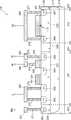
도 1은 일 예에 따른 불휘발성 메모리장치를 나타내 보인 회로도이다.
도 2는 도 1의 불휘발성 메모리장치의 메모리셀의 일 예를 나타내 보인 단면도이다.
도 3은 도 1의 불휘발성 메모리장치의 프로그램 동작을 설명하기 위해 나타내 보인 회로도이다.
도 4는 도 1의 불휘발성 메모리장치의 프로그램 과정에서 서로 다른 특성을 갖는 셀 트랜지스터들의 프로그램 동작을 비교하기 위해 나타내 보인 도면이다.
도 5는 다른 예에 따른 불휘발성 메모리장치를 나타내 보인 회로도이다.
도 6은 도 5의 불휘발성 메모리장치의 프로그램 동작을 설명하기 위해 나타내 보인 회로도이다.
도 7은 또 다른 예에 따른 불휘발성 메모리장치를 나타내 보인 회로도이다.
도 8은 도 7의 불휘발성 메모리장치의 메모리셀의 일 예를 나타내 보인 단면도이다.
도 9는 도 7의 불휘발성 메모리장치의 프로그램 동작을 설명하기 위해 나타내 보인 회로도이다.
도 10은 또 다른 예에 따른 불휘발성 메모리장치를 나타내 보인 회로도이다.
도 11은 도 10의 불휘발성 메모리장치의 프로그램 동작을 설명하기 위해 나타내 보인 회로도이다.1 is a circuit diagram showing a nonvolatile memory device according to an example.
2 is a cross-sectional view showing an example of a memory cell of the nonvolatile memory device of FIG.
3 is a circuit diagram showing a program operation of the nonvolatile memory device of FIG.
FIG. 4 is a diagram for comparing programming operations of cell transistors having different characteristics in the programming process of the nonvolatile memory device of FIG. 1. Referring to FIG.
5 is a circuit diagram showing a nonvolatile memory device according to another example.
6 is a circuit diagram showing the program operation of the nonvolatile memory device of FIG.
7 is a circuit diagram showing a nonvolatile memory device according to another example.
8 is a cross-sectional view showing an example of a memory cell of the nonvolatile memory device of FIG.
9 is a circuit diagram for explaining a program operation of the nonvolatile memory device of FIG.
10 is a circuit diagram showing a nonvolatile memory device according to another example.
11 is a circuit diagram for explaining the programming operation of the nonvolatile memory device of FIG.
불휘발성 메모리장치는 웨이퍼 단위로 제조가 이루어질 수 있다. 집적도에 따라 달라지기는 하지만, 한장의 웨이퍼에 적게는 수백개에서 많게는 수만개의 메모리소자들이 집적될 수 있다. 웨이퍼 단위로 제조공정이 이루어짐에 따라, 웨이퍼의 위치에 따른 제조공정의 편차로 인해, 불휘발성 메모리장치들은 각각 균일하지 않는 특성을 가질 수 있다. 이와 같은 균일하지 않는 특성으로 인하여, 불휘발성 메모리장치를 프로그램시키는 경우 균일하지 않는 문턱전압 분포를 나타낸다. 문턱전압 편차가 임계치 이내인 경우 프로그램 알고리듬(algorithm)의 다양한 변화 등을 통해 정상적인 동작이 이루어지도록 할 수 있지만, 문턱전압 편차가 큰 경우 정상적인 동작이 어려운 경우도 발생할 수 있다. 본 출원의 여러 실시예에서는 불휘발성 메모리장치의 프로그램 동작시 셀트랜지스터의 전류값과 기준값을 비교하고 그 결과에 따라 셀트랜지스터의 커플링 바이어스 인가를 제어함으로써, 프로그램이 이루어진 셀트랜지스터들이 균일한 문턱전압값을 갖도록 할 수 있다.The nonvolatile memory device can be manufactured on a wafer-by-wafer basis. Depending on the degree of integration, hundreds to tens of thousands of memory devices may be integrated on a single wafer. As the fabrication process is performed on a wafer-by-wafer basis, due to variations in the manufacturing process depending on the position of the wafer, the non-volatile memory devices may each have non-uniform characteristics. Due to this non-uniform nature, non-volatile memory devices exhibit an uneven threshold voltage distribution when programmed. When the threshold voltage deviation is within the threshold value, normal operation can be performed through various changes of the program algorithm. However, when the threshold voltage deviation is large, normal operation may be difficult. In the embodiments of the present invention, the comparison of the current value of the cell transistor with the reference value in the program operation of the nonvolatile memory device and the application of the coupling bias of the cell transistor is controlled according to the result, Value.
본 출원의 예의 기재에서 "제1" 및 "제2"와 같은 기재는 부재를 구분하기 위한 것이며, 부재 자체를 한정하거나 특정한 순서를 의미하는 것으로 사용된 것은 아니다. 또한, 어느 부재의 "상"에 위치하거나 "상부", "하부", 또는 "측면"에 위치한다는 기재는 상대적인 위치 관계를 의미하는 것이지 그 부재에 직접 접촉하거나 또는 사이 계면에 다른 부재가 더 도입되는 특정한 경우를 한정하는 것은 아니다. 또한, 어느 한 구성 요소가 다른 구성 요소에 "연결되어 있다"거나 "접속되어 있다"의 기재는, 다른 구성 요소에 전기적 또는 기계적으로 직접 연결되어 있거나 또는 접속되어 있을 수 있으며, 또는, 중간에 다른 별도의 구성 요소들이 개재되어 연결 관계 또는 접속 관계를 구성할 수도 있다.In the description of the examples of the present application, descriptions such as " first "and" second "are for distinguishing members, and are not used to limit members or to denote specific orders. Further, the description that a substrate located on the "upper", "lower", or "side" of a member means a relative positional relationship means that the substrate is in direct contact with the member, or another member The present invention is not limited to a particular case. It is also to be understood that the description of "connected" or "connected" to one component may be directly or indirectly electrically or mechanically connected to another component, Separate components may be interposed to form a connection relationship or a connection relationship.
도 1은 일 예에 따른 불휘발성 메모리장치를 나타내 보인 회로도이다. 도 1을 참조하면, 불휘발성 메모리장치(100)는, 메모리셀(110)과, 스위칭부(120)와, 비교부(130)와, 그리고 그라운드연결부(140)를 포함하여 구성된다. 메모리셀(110)은, 셀 트랜지스터(112), 선택 트랜지스터(114), 및 커플링 커패시터(116)를 포함한다. 일 예에서 셀 트랜지스터(112) 및 선택 트랜지스터(114)는, 각각 n채널형 모스 전계효과트랜지스터로 구성될 수 있다. 셀 트랜지스터(112)는 플로팅게이트단자(FG)를 가지며, 선택 트랜지스터(114)는 선택게이트단자(G2)를 갖는다. 셀 트랜지스터(112)의 드레인단자(D1)와 선택 트랜지스터(120)의 소스단자(S2)는 상호 결합된다. 선택 트랜지스터(114)의 선택게이트단자(G2) 및 드레인단자(D2)는, 각각 워드라인(WL) 및 비트라인(BL)에 결합된다. 셀 트랜지스터(111)의 소스단자(S1)는 소스라인(SL)에 결합된다. 셀 트랜지스터(111)의 플로팅게이트단자(FG)는 커플링 커패시터(116)에 결합된다. 일 예에서 커플링 커패시터(116)는 모스 커패시터 구조로 구성될 수 있다.1 is a circuit diagram showing a nonvolatile memory device according to an example. Referring to FIG. 1, a
스위칭부(120)는, 바이어스 인가단자(CG) 및 커플링 커패시터(116) 사이에 배치된다. 스위칭부(120)는, 바이어스 인가단자(CG)와 커플링 커패시터(116)를 전기적으로 단락시키거나 개방시키는 스위칭소자(122)를 포함할 수 있다. 일 예에서 스위칭소자(122)는 모스 전계효과트랜지스터로 구현될 수 있지만, 이는 단지 하나의 예로서 스위칭동작을 수행할 수 있는 다른 여러 소자들 중 하나로 구현될 수도 있다. 스위칭소자(122)가 스위칭 온(switching on) 되는 동안, 즉 바이어스 인가단자(CG)와 커플링 커패시터(116)가 전기적으로 단락되어 있는 동안에는, 셀 트랜지스터(114)의 플로팅게이트단자(FG)로 바이어스 인가단자(CG)에 인가되는 바이어스 전압에 커플링되는 커플링 전압이 유도된다. 플로팅게이트단자(FG)에 유도되는 커플링 전압은 커플링 커패시터(116)가 갖는 커플링 비(coupling ratio)에 의해 결정될 수 있다. 스위칭소자(122)가 스위칭 오프(switching off) 되는 동안, 즉 바이어스 인가단자(CG)와 커플링 커패시터(116)가 전기적으로 개방되어 있는 동안에는, 셀 트랜지스터(114)의 플로팅게이트단자(FG)에 커플링 전압이 유도되지 않는다.The
비교부(130)는, 비교기(132)와 기준전류를 발생시키는 정전류원(134)을 포함하여 구성될 수 있다. 비교기(132)는, 메모리셀(110)에 흐르는 전류가 입력되는 제1 입력단자와, 정전류원(134)으로부터의 기준전류가 입력되는 제2 입력단자와, 그리고 출력단자를 갖는 전류비교기로 구성될 수 있다. 정전류원(134)에 의해 발생되는 기준전류는, 프로그램 동작에 의해 메모리셀(110)이 가질 수 있는 여러 문턱전압값들 중에서 타겟(target) 문턱전압값에 대응되는 전류값으로 설정될 수 있다. 일 예에서 메모리셀(110)에 흐르는 전류가 기준전류보다 큰 경우, 비교기(132)는 하이(high) 레벨의 출력신호(OUT)를 출력시킨다. 반면에 기준전류가 메모리셀(110)에 흐르는 전류보다 큰 경우, 비교기(132)는 로우(low) 레벨의 출력신호(OUT)를 출력시킨다.The
비교기(132)로부터의 출력신호(OUT)는 스위칭부(120)에 전달되어 스위칭소자(122)를 스위칭 온 시키거나, 또는 스위칭 오프시킨다. 일 예에서 메모리셀(110)에 흐르는 전류가 기준전류보다 큰 시간 동안에 비교기(132)로부터 출력되는 하이 레벨의 출력신호(OUT)는 스위칭소자(122)를 스위칭 온 상태로 유지되도록 한다. 따라서 이 기간 동안에 바이어스 입력단자(CG)로부터 입력되는 바이어스전압이 커플링 커패시터(116)에 인가된다. 반면에 메모리셀(110)에 흐르는 전류가 기준전류보다 작아지게 되면, 비교기(132)로부터 로우 레벨의 출력신호(OUT)가 출력되고, 이 로우 레벨의 출력신호(OUT)는 스위칭 소자(122)를 스위칭 오프 시킨다. 따라서 바이어스 입력단자(CG)로부터 입력되는 바이어스전압은 커플링 커패시터(116)에 인가되지 않는다.The output signal OUT from the
그라운드연결부(140)는, 메모리셀(110)과 그라운드단자(GND) 사이에 배치된다. 그라운드연결부(140)는, n채널형 모스 전계효과트랜지스터(142)로 구성될 수 있다. n채널형 모스 전계효과트랜지스터(142)는, 게이트단자(G3), 드레인단자(D3), 및 소스단자(S3)를 갖는다. 게이트단자(G3)에는 게이트제어신호가 입력되며, 이 게이트제어신호에 의해 n채널형 모스 전계효과트랜지스터(142)는 턴 온되거나 턴 오프된다. 프로그램 동작이 이루어지는 동안 n채널형 모스 전계효과트랜지스터(142)는 턴 오프되며, 리드 동작이 이루어지는 동안 n채널형 모스 전계효과트랜지스터(142)는 턴 온 된다. 드레인단자(D3)는 소스라인(SL)을 통해 셀 트랜지스터(114)의 소스단자(S1)에 결합된다. 또한 드레인단자(D3)는, 비교기(132)의 제1 입력단자에도 결합된다. 소스단자(S3)는 그라운드단자(GND)에 결합된다. n채널형 모스 전계효과트랜지스터(142)가 턴 온 되면, 셀 트랜지스터(112)의 소스단자(S1)가 결합되는 소스라인(SL)은 그라운드단자(GND)에 결합되며, 따라서 셀 트랜지스터(112)의 소스단자(S1)에는 그라운드 전압인 0V가 인가된다. 소스라인(SL)에 그라운드 전압이 인가되는 리드 동작 동안에는 n채널형 모스 전계효과트랜지스터(142)의 턴 온 상태가 유지된다. 반면에 n채널형 모스 전계효과트랜지스터(142)가 턴 오프 되면, 소스라인(SL)은 비교기(132)의 제1 입력단자에 결합된다. 따라서 이 경우 비교기(132)의 제1 입력단자에는 셀 트랜지스터(112)에 흐르는 전류가 입력된다. 프로그램 전류를 검출하여 셀 트랜지스터(112)의 문턱전압값을 균일하게 하기 위해, 프로그램 동작 동안에는 n채널형 모스 전계효과트랜지스터(142)의 턴 오프 상태가 유지된다.The
도 2는 도 1의 불휘발성 메모리장치의 메모리셀의 일 예를 나타내 보인 단면도이다. 본 예에 따른 불휘발성 메모리장치의 메모리셀(110)은, 싱글 폴리 메모리셀(single poly memory cell)일 수 있다. 구체적으로, 기판(210) 상부 영역에 n형의 딥웰(DNW; Deep N Well)(212)이 배치된다. 기판(210)은 p형의 도전형을 가질 수 있다. 기판(210)은, 메모리셀 영역(201), 커플링 영역(202), 및 아이솔레이션 영역들(203, 204, 205)을 갖는다. 아이솔레이션 영역들(203, 204) 각각은 메모리셀 영역(201)의 양 측면에 배치된다. 아이솔레이션 영역들(204, 205) 각각은 커플링 영역(202) 양 측면에 배치된다. n형의 딥웰(212)의 상부 영역에는 p형의 제1 웰영역(231) 및 p형의 제2 웰영역(232)이 상호 이격되도록 배치된다. p형의 제1 웰영역(231)은, 메모리셀 영역(201) 내에 배치된다. p형의 제2 웰영역(232)은 커플링 영역(202) 내에 배치된다. 아이솔레이션 영역(203)의 n형의 딥웰(212) 상부영역에는 n형의 제1 웰영역(233)이 배치된다. 아이솔레이션 영역(204)의 n형의 딥웰(212) 상부영역에는 n형의 제2 웰영역(234)이 배치된다. 아이솔레이션 영역(205)의 n형의 딥웰(212) 상부영역에는 n형의 제3 웰영역(235)이 배치된다.2 is a cross-sectional view showing an example of a memory cell of the nonvolatile memory device of FIG. The
p형의 제1 웰영역(231) 상부와 p형의 제2 웰영역(232) 상부에는 제1 게이트절연층(241) 및 플로팅게이트층(251)이 배치된다. p형의 제1 웰영역(231) 상부에는 제2 게이트절연층(242) 및 선택게이트층(252)이 배치된다. 제1 게이트절연층(241) 및 플로팅게이트층(251)과, 제2 게이트절연층(242) 및 선택게이트층(252)은 일정 간격 상호 이격되도록 배치된다. 비록 도면에서 플로팅게이트층(251)은 서로 분리되어 있는 것으로 도시되어 있지만, 본 단면 구조에서 나타나지 않는 다른 부분에서 서로 연결된다.A first
n형의 제1 웰영역(233)의 상부영역에는 n+형의 웰컨택영역(261)이 배치된다. p형의 제1 웰영역(231) 상부영역에는, n+형의 소스영역(262), n+형의 드레인영역(263), n+형의 접합영역(264)이 상호 이격되도록 배치된다. n+형의 소스영역(262) 및 n+형의 접합영역(264)은 플로팅게이트층(251)의 양 측면에 정렬되도록 배치된다. n+형의 드레인영역(263) 및 n+형의 접합영역(264)은 선택게이트층(252)의 양 측면에 정렬되도록 배치된다. 따라서 n+형의 접합영역(264)은, p형의 제1 웰영역(231) 상부영역에서 플로팅게이트층(251)과 선택게이트층(252) 사이에 배치된다. p형의 제1 웰영역(231) 상부영역에는 p+형의 제1 컨택영역(265)이 n+형의 소스영역(262)과 일정 간격 이격되도록 배치된다. p형의 제2 웰영역(232) 상부영역에는 p+형의 제2 컨택영역(266)과 n+형의 컨택영역(267)이 상호 이격되도록 배치된다. p+형의 제2 컨택영역(266)과 n+형의 컨택영역(267)은, p형의 제2 웰영역(232) 상부의 플로팅게이트층(251)의 양 측면들에 각각 정렬되도록 배치된다.An n + -type
n+형의 웰컨택영역(261)은 제1 컨택플러그(271)를 통해 제1 배선층패턴(281)에 전기적으로 결합된다. 제1 배선층패턴(281)은 웰바이어스라인(WBL)에 결합된다. 웰바이어스라인(WBL)을 통해 인가되는 바이어스는, 아이솔레이션 기능을 수행할 수 있는 크기를 가지며, n형의 제1 웰영역(233), n형의 제2 웰영역(234), 및 n형의 제3 웰영역(235)에 전달된다. 딥웰(212)과, p+형의 제1 컨택영역(265) 및 n+형의 소스영역(262)은, 각각 제2 컨택플러그(272) 및 제3 컨택플러그(273)를 통해 제2 배선층패턴(282)에 전기적으로 결합된다. 제2 배선층패턴(282)은 소스라인(SL)에 결합된다. 선택게이트층(252)은 제4 컨택플러그(274)를 통해 제3 배선층패턴(283)에 전기적으로 결합된다. 제3 배선층패턴(283)은 워드라인(WL)에 결합된다. n+형의 드레인영역(263)은 제5 컨택플러그(275)를 통해 제4 배선층패턴(284)에 전기적으로 결합된다. 제4 배선층패턴(284)은 비트라인(BL)에 결합된다. p+형의 제2 컨택영역(266) 및 n+형의 컨택영역(267)은, 각각 제6 컨택플러그(276) 및 제7 컨택플러그(277)를 통해 제5 배선층패턴(285)에 전기적으로 결합된다. 제5 배선층패턴(285)은 바이어스 인가단자(CG)에 결합된다. p형의 제2 웰영역(232)과, 그 위에 배치되는 제1 게이트절연층패턴(241) 및 플로팅게이트층(251)은, 커플링 커패시터(116)를 구성한다.The n + -type
메모리셀 영역(201) 내의 p형의 제1 웰영역(231), n+형의 소스영역(262), n+형의 접합영역(264), 제1 게이트절연층(241), 및 플로팅게이트층(251)은, 도 1의 메모리셀(110)의 셀 트랜지스터(112)를 구성한다. 메모리셀 영역(201) 내의 p형의 제1 웰영역(231), n+형의 드레인영역(263), n+형의 접합영역(264), 제2 게이트절연층(242), 및 선택게이트층(252)은, 도 1의 메모리셀(110)의 선택 트랜지스터(114)를 구성한다. n+형의 접합영역(264)은, 셀 트랜지스터(도 1의 112)의 드레인영역으로 작용하면서, 동시에 선택 트랜지스터(도 1의 114)의 소스영역으로도 작용한다. 커플링 영역(202) 내의 p형의 제2 웰영역(232), 제1 게이트절연층(241), 및 플로팅게이트층(251)은, 도 1의 메모리셀(110)의 커플링 커패시터(116)를 구성한다.The p + -type
메모리셀(110)의 프로그램 동작 수행을 위해, 워드라인(WL)에 게이트 턴온 전압을 인가한다. 바이어스 인가단자(CG)에는 포지티브 프로그램전압을 인가한다. 비트라인(BL)에는 포지티브 비트라인전압을 인가한다. p형의 제1 웰영역(231) 및 p형의 제2 웰영역(232)에는 그라운드전압을 인가한다. 바이어스 인가단자(CG)로부터의 포지티브 프로그램전압은, p형의 제2 웰영역(232)에 인가된다. 커플링 커패시터(116)의 커플링 동작에 의해, 플로팅게이트층(251)에는 p형의 제2 웰영역(232)에 인가되는 포지티브 프로그램전압에 커플링된 커플링 프로그램전압이 유도된다. 워드라인(WL)에 인가되는 게이트 턴온 전압은 선택 트랜지스터를 턴 온 시킨다. 이에 따라 턴 온 된 선택 트랜지스터에 연결된 셀 트랜지스터가 선택된다. 선택 트랜지스터가 턴 온 됨에 따라, n+형의 드레인영역(263) 및 n+형의 접합영역(264) 사이에는 반전층(inversion layer)이 형성되고, 이에 따라 n+형의 접합영역(264)에는 비트라인(BL)으로부터의 포지티브 비트라인전압이 전달된다. 한편, 플로팅게이트층(251)에 커플링 프로그램전압이 유도되며, 셀 트랜지스터도 턴 온 된다. 즉, n+형의 소스영역(262) 및 n+형의 접합영역(264) 사이에 반전층이 형성된다. 플로팅게이트층(251)에 커플링 프로그램전압이 유도되고, p형의 제1 웰영역(231)에는 그라운드 바이어스가 인가됨에 따라, 플로팅게이트층(251)과 반전층 사이에는 커플링 프로그램전압에 해당하는 전위차가 생긴다. 이 전위차에 의해 반전층 내의 캐리어들, 즉 전자들이 제1 게이트절연층(241)을 통과하여 플로팅게이트층(251)으로 터널링하는 F-N 터널링(Fowler-Nordheim tunneling) 메커니즘에 의한 프로그램 동작이 이루어진다. 프로그램 동작이 수행되는 동안, 즉 플로팅게이트층(251)으로 전자들이 터널링되는 동안 플로팅게이트층(251)에 가해지는 전압은 떨어진다. 전압이 감소됨에 따라 n+형의 드레인영역(263)으로부터 n+형의 접합영역(264)을 통해 n+형의 소스영역(262)으로 흐르는, 즉 비트라인(BL)으로부터 소스라인(SL)으로 흐르는 전류량은 감소된다.In order to perform the programming operation of the
도 3은 도 1의 불휘발성 메모리장치의 프로그램 동작을 설명하기 위해 나타내 보인 회로도이다. 도 3에서 도 1과 동일한 참조부호는 동일한 구성요소를 나타내며, 따라서 이하에서 중복되는 설명은 생략하기로 한다. 도 3을 참조하면, 셀 트랜지스터(112)에 대한 프로그램 동작을 수행하기 위해, 선택 트랜지스터(114)의 워드라인(WL)을 통해 선택게이트단자(G2)에 게이트 턴온전압(+VG)을 인가하고, 비트라인(BL)에는 프로그램 비트라인전압(+VBL1)을 인가한다. 이에 따라 선택 트랜지스터(114)는 턴 온 되어 셀 트랜지스터(112)가 선택된다. 스위칭소자(122)가 스위칭 온 상태, 즉 스위칭소자(122)가 닫힌 상태에서 바이어스 인가단자(CG)를 통해 포지티브 프로그램전압(+VPP1)을 인가한다. 커플링 커패시터(116)의 커플링 동작에 의해, 셀 트랜지스터(112)의 플로팅게이트단자(FG)에는 포지티브 프로그램전압(+VPP1)에 커플링된 커플링 전압이 인가된다. 포지티브 프로그램전압(+VPP1)은, 커플링 전압에 의해 셀 트랜지스터(112)에서 F-N 터널링이 이루어질 수 있는 정도의 크기를 갖는다. 일 예에서 커플링 커패시터(116)의 커플링 비(coupling ratio)가 대략 90% 이상인 경우, 포지티브 프로그램전압(+VPP1)은 대략 16V일 수 있다. 셀 트랜지스터(112)에 대한 프로그램 동작이 이루어지는 동안, 그라운드연결부(140)를 구성하는 n채널형 모스 전계효과트랜지스터(142)는 턴 오프된다.3 is a circuit diagram showing a program operation of the nonvolatile memory device of FIG. In FIG. 3, the same reference numerals as those in FIG. 1 denote the same components, and a duplicate description will be omitted below. 3, a gate turn-on voltage (+ VG) is applied to the select gate terminal G2 through the word line WL of the
이와 같은 프로그램 과정에서, 셀 트랜지스터(112)의 드레인단자(D1) 및 소스단자(S1) 사이와, 선택 트랜지스터(114)의 드레인단자(D2) 및 소스단자(S2) 사이에는 각각 반전층이 형성된다. 셀 트랜지스터(112)에서는 반전층 내의 전자들이 플로팅게이트단자(FG)로 터널링되고, 이에 따라 셀 트랜지스터(112)의 문턱전압값은 타겟 문턱전??값을 향해 변화된다. 이 과정에서 비트라인(BL)으로부터 선택 트랜지스터(114) 및 셀 트랜지스터(112)를 통해 비교기(132)의 제1 입력단자로 프로그램 전류(Ip)가 흐른다. 프로그램 전류(Ip)는, 셀 트랜지스터(112)의 변화하는 문턱전압값에 따라 그 값이 변화한다. 플로팅게이트단자(FG)로의 전자들의 터널링이 이루어짐에 따라 셀 트랜지스터(112)의 문턱전압값은 점점 커지고, 이에 따라 프로그램 전류(Ip)의 크기는 점점 작아진다.In such a program process, an inversion layer is formed between the
비교기(132)는, 제1 입력단자로 흐르는 프로그램 전류(Ip)의 값과, 정전류원(134)으로부터 제2 입력단자로 흐르는 기준 전류(Iref)의 값을 비교한다. 기준 전류(Iref)는, 프로그램 동작에 의해 셀 트랜지스터(112)가 가질 수 있는 문턱전압값들 중에서 타겟 문턱전압값에 대응되는 전류값으로 설정된다. 프로그램 전류(Ip) 값이 기준 전류(Iref) 값보다 큰 구간에서는, 셀 트랜지스터(112)의 문턱전압값이 타겟 문턱전압값까지 아직 도달하지 않은 상태를 의미한다. 프로그램 전류(Ip) 값이 기준 전류(Iref) 값과 동일한 시점에서는, 셀 트랜지스터(112)의 문턱전압값이 타겟 문턱전압값과 동일한 상태를 의미한다. 프로그램 전류(Ip) 값이 기준 전류(Iref) 값보다 작은 구간에서는, 셀 트랜지스터(112)의 문턱전압값이 타겟 문턱전압값보다 커진 상태를 의미한다.The
비교기(132)는, 프로그램 전류(Ip) 값이 기준 전류(Iref) 값보다 큰 동안 하이 레벨의 출력신호(OUT)를 발생시킨다. 반면에 프로그램 전류(Ip) 값이 기준 전류(Iref) 값보다 작은 동안에는 로우 레벨의 출력신호(OUT)를 발생시킨다. 하이 레벨의 출력신호(OUT)는, 스위칭소자(122)를 스위칭 온 상태를 유지시킨다. 다라서 셀 트랜지스터(112)의 플로팅게이트단자(FG)에 커플링전압이 계속 유도되며, 셀 트랜지스터(112)에 대한 프로그램 동작이 유지된다. 비교기(132)로부터 로우 레벨의 출력신호(OUT)가 발생되게 되면, 즉 셀 트랜지스터(112)의 문턱전??값이 타겟 문턱전압값에 도달되게 되면, 로우 레벨의 출력신호(OUT)에 의해 스위칭소자(122)는 스위칭 온 상태에서 스위칭 오프 상태가 된다. 이에 따라 바이어스 인가단자(CG)와 커플링 커패시터(116)의 전기적 연결라인은 개방(open)된다. 셀 트랜지스터(112)의 플로팅게이트단자(FG)에는 더 이상 커플링전압이 유도되지 못하고, 그 결과 셀 트랜지스터(112)의 프로그램 동작은 종료된다. 비교기(132)로부터의 출력신호(OUT)의 레벨은 서로 반대가 될 수도 있다. 이 경우 출력신호(OUT)의 레벨에 따른 스위칭소자(122)의 스위칭동작 또한 반대가 된다.The
도 4는 도 1의 불휘발성 메모리장치의 프로그램 과정에서 서로 다른 특성을 갖는 셀 트랜지스터들의 프로그램 동작을 비교하기 위해 나타내 보인 도면이다. 본 예에서 비교 대상인 제1 셀 트랜지스터(CELL A)와 제2 셀 트랜지스터(CELL B)는, 각각 도 1 내지 도 3을 참조하여 설명한 구조 및 등가회로와 동일한 구조 및 등가회로로 구성되며, 단지 그 제조과정에서 서로 다른 특성을 나타는 셀 트랜지스터들이다. 이와 같은 서로 다른 특성은, 게이트절연층의 두께 차이나, 또는 접합영역에서의 도핑 농도의 편차 등의 원인에 의해 유발될 수 있다. 도 4를 도 3과 함께 참조하면, 제1 셀 트랜지스터(CELL A)와 제2 셀 트랜지스터(CELL B)를 모두 선택하여 두 셀 트랜지스터들에 대한 프로그램 동작을 제1 시점(T1)에서 동시에 수행되도록 할 수 있다. 프로그램 동작이 수행되는 과정에서, 제1 셀 트랜지스터(CELL A)에 흐르는 프로그램 전류(Ip)가 기준 전류(Iref)보다 큰 동안에는 제1 셀 트랜지스터(CELL A)에 연결된 비교기(132)가 하이(HIGH) 레벨의 출력신호(OUT1)를 유지하며, 이에 따라 제1 셀 트랜지스터(CELL A)에 대한 프로그램 동작이 유지된다. 마찬가지로 제2 셀 트랜지스터(CELL B)에 흐르는 프로그램 전류(Ip)가 기준 전류(Iref)보다 큰 동안에도 제2 셀 트랜지스터(CELL B)가 연결된 비교기(132)가 하이(HIGH) 레벨의 출력신호(OUT2)를 유지하며, 이에 따라 제2 셀 트랜지스터(CELL B)에 대한 프로그램 동작 또한 유지된다.FIG. 4 is a diagram for comparing programming operations of cell transistors having different characteristics in the programming process of the nonvolatile memory device of FIG. 1. Referring to FIG. In this example, the first cell transistor CELL A and the second cell transistor CELL B to be compared are configured with the same structure and equivalent circuit as those of the structure and the equivalent circuit described with reference to Figs. 1 to 3, They are cell transistors that exhibit different characteristics in the manufacturing process. These different characteristics may be caused by a difference in the thickness of the gate insulating layer or a variation in the doping concentration in the junction region. Referring to FIG. 4 together with FIG. 3, the first cell transistor CELL A and the second cell transistor CELL B are both selected to perform a program operation for two cell transistors at a first
앞서 언급한 바와 같이, 제1 셀 트랜지스터(CELL A)와 제2 셀 트랜지스터(CELL B)은 서로 다른 특성을 가지며, 이에 따라 동일한 바이어스 조건하에서 제1 셀 트랜지스터(CELL A)의 문턱전압값이 타겟 문턱전??값에 도달하는 시점과, 제2 셀 트랜지스터(CELL B)의 문턱전압값이 타겟 문턱전압값에 도달하는 시점은 다를 수 있다. 그럼에도 불구하고, 제1 셀 트랜지스터(CELL A)에 대한 프로그램 동작과 제2 셀 트랜지스터(CELL B)에 대한 프로그램 동작을 동일한 시간 동안 수행하게 되면, 프로그램된 두 셀 트랜지스터들이 갖는 문턱전압값들의 편차가 커지며, 따라서 이 셀 트랜지스터들로 구성되는 셀 어레이의 동작 편차도 함께 커진다.As described above, the first cell transistor CELL A and the second cell transistor CELL B have different characteristics, and therefore, under the same bias condition, the threshold voltage value of the first cell transistor CELL A becomes the target The time point when the threshold voltage value reaches the threshold voltage value and the time point at which the threshold voltage value of the second cell transistor CELL B reaches the target threshold voltage value may be different. Nevertheless, when the program operation for the first cell transistor CELL A and the program operation for the second cell transistor CELL B are performed for the same time, the deviation of the threshold voltage values of the programmed two-cell transistors So that the operating deviation of the cell array composed of these cell transistors also increases.
본 예에서는 이와 같은 문제를 방지하기 위해, 제1 셀 트랜지스터(CELL A)의 프로그램 전류(Ip)가 기준 전류(Iref)보다 작아지기 시작하는 시점(T2)에 제1 셀 트랜지스터(CELL A)에 연결된 비교기(132)의 출력신호(OUT1)는 하이(HIGH) 레벨의 출력신호로부터 로우(LOW) 레벨의 출력신호로 전환된다. 그 결과 제1 셀 트랜지스터(CELL A)에 연결된 스위칭소자(122)는 스위칭 오프되고, 제1 셀 트랜지스터(CELL A)에 대한 프로그램 동작은 종료된다. 이 시점(T2)에서 제2 셀 트랜지스터(CELL B)의 경우 프로그램 전류(Ip)가 기준 전류(Iref)보다 여전히 클 수 있다. 따라서 제2 셀 트랜지스터(CELL B)에 연결된 비교기(132)의 출력신호(OUT2)는 하이(HIGH) 레벨의 출력신호를 유지하고, 그 결과 제2 셀 트랜지스터(CELL B)에 대한 프로그램 동작은 계속 수행된다. 제2 셀 트랜지스터(CELL B)의 프로그램 전류(Ip)가 기준 전류(Iref)보다 작아지기 시작하는 시점(T3)에 제2 셀 트랜지스터(CELL B)에 연결된 비교기(132)의 출력신호(OUT2)는 하이(HIGH) 레벨의 출력신호로부터 로우(LOW) 레벨의 출력신호로 전환된다. 그 결과 제2 셀 트랜지스터(CELL B)에 연결된 스위칭소자(122)는 스위칭 오프되고, 제2 셀 트랜지스터(CELL B)에 대한 프로그램 동작은 종료된다. 이와 같은 프로그램 동작 제어를 통해, 서로 다른 특성의 제1 셀 트랜지스터(CELL A) 및 제2 셀 트랜지스터(CELL B)가 동일한 크기의 문턱전압을 나타내도록 할 수 있다.In order to prevent such a problem, in this example, the first cell transistor CELL A is connected to the first cell transistor CELL A at a time point T2 at which the program current Ip of the first cell transistor CELL A starts to become smaller than the reference current Iref The output signal OUT1 of the connected
도 5는 다른 예에 따른 불휘발성 메모리장치를 나타내 보인 회로도이다. 도 5를 참조하면, 불휘발성 메모리장치(300)는, 메모리셀(310)과, 스위칭부(320)와, 전류전달부(330)와, 비교부(340), 그라운드연결부(350)를 포함하여 구성된다. 메모리셀(310)은, 셀 트랜지스터(312), 선택 트랜지스터(314), 및 커플링 커패시터(316)를 포함한다. 일 예에서 셀 트랜지스터(312) 및 선택 트랜지스터(314)는 n채널형 모스 전계효과트랜지스터로 구성될 수 있다. 셀 트랜지스터(312)는 플로팅게이트단자(FG)를 가지며, 선택 트랜지스터(314)는 선택게이트단자(G2)를 갖는다. 셀 트랜지스터(312)의 드레인단자(D1)와 선택 트랜지스터(314)의 소스단자(S2)는 상호 결합된다. 선택 트랜지스터(314)의 선택게이트단자(G2) 및 드레인단자(D2)는, 각각 워드라인(WL) 및 비트라인(BL)에 결합된다. 셀 트랜지스터(311)의 소스단자(S1)는 소스라인(SL)에 결합된다. 셀 트랜지스터(312)의 플로팅게이트단자(FG)는 커플링 커패시터(316)에 결합된다. 일 예에서 커플링 커패시터(316)는 모스 커패시터 구조로 구성될 수 있다. 메모리셀(310)의 단면 구조는 도 2를 참조하여 설명한 메모리셀(110)의 단면 구조와 동일할 수 있다.5 is a circuit diagram showing a nonvolatile memory device according to another example. 5, the
스위칭부(320)는, 바이어스 인가단자(CG) 및 커플링 커패시터(316) 사이에 배치된다. 스위칭부(320)는, 바이어스 인가단자(CG)와 커플링 커패시터(316)를 전기적으로 단락시키거나 개방시키는 스위칭소자(322)를 포함할 수 있다. 일 예에서 스위칭소자(322)는 모스 전계효과트랜지스터로 구현될 수 있지만, 이는 단지 하나의 예로서 스위칭동작을 수행할 수 있는 다른 여러 소자들 중 하나로 구현될 수도 있다. 스위칭소자(322)가 스위칭 온(switching on) 되는 동안, 즉 바이어스 인가단자(CG)와 커플링 커패시터(316)를 전기적으로 단락시키는 동안에는, 바이어스 인가단자(CG)에 인가되는 바이어스 전압에 커플링되는 커플링 전압이 셀 트랜지스터(314)의 플로팅게이트단자(FG)에 유도된다. 플로팅게이트단자(FG)에 유도되는 커플링 전압은 커플링 비(coupling ratio)에 의해 결정될 수 있다. 스위칭소자(322)가 스위칭 오프(switching off) 되는 동안, 즉 바이어스 인가단자(CG)와 커플링 커패시터(316)가 전기적으로 개방되어 있는 동안에는, 셀 트랜지스터(314)의 플로팅게이트단자(FG)에는 커플링 전압이 유도되지 않는다.The switching
전류전달부(330)는, 메모리셀(310)을 흐르는 전류를 비교부(340)에 전달한다. 전류전달부(330)는, 제1 모스 전계효과트랜지스터(332) 및 제2 모스 전계효과트랜지스터(334)로 구성되는 전류 미러(current mirror) 회로를 포함할 수 있다. 전류 미러 회로는 부하(load) 상태에 영향을 받지 않고 출력전류를 발생시킬 수 있다는 장점을 갖는다. 제1 모스 전계효과트랜지스터(332)의 게이트단자(G4)와 제2 모스 전계효과트랜지스터(334)의 게이트단자(G5)는 서로 결합된다. 제1 모스 전계효과트랜지스터(332)의 소스단자(S4)와 제2 모스 전계효과트랜지스터(334)의 소스단자(S5)는 그라운드단자(GND)에 공통으로 결합된다. 제1 모스 전계효과트랜지스터(332)의 드레인단자(D4)는 셀 트랜지스터(312)의 소스단자(S1) 및 제1 모스 전계효과트랜지스터(332)의 게이트단자(G4)에 결합된다. 제2 모스 전계효과트랜지스터(334)의 드레인단자(D5)는 비교부(340)에 결합된다. 제2 모스 전계효과트랜지스터(334)의 드레인단자(D5)로부터 소스단자(S4)로 흐르는 전류(Ipb)는, 제1 모스 전계효과트랜지스터(332)의 드레인단자(D4)로부터 소스단자(S4)로 흐르는 전류(Ipa)와 같은 크기를 갖는다.The
비교부(340)는, 비교기(342)와 기준전류를 발생시키는 정전류원(344)을 포함하여 구성될 수 있다. 비교기(342)는, 제1 입력단자 및 제2 입력단자와, 그리고 출력단자를 갖는 전류비교기로 구성될 수 있다. 제1 입력단자는 전류전달부(330)의 제2 모스 전계효과트랜지스터(334)의 드레인단자(D5)에 결합된다. 제2 입력단자는 기준전류(Iref)를 발생시키는 정전류원(344)과 결합된다. 출력단자(OUT)는 스위칭부(320)와 결합된다. 정전류원(334)에 의해 발생되는 기준전류(Iref)는, 프로그램 동작에 의해 메모리셀(310)이 가질 수 있는 여러 문턱전압값들 중에서 타겟(target) 문턱전압값에 대응되는 전류값으로 설정될 수 있다. 일 예에서 메모리셀(310)에 흐르는 전류(Ipa=Ipb)가 기준전류(Iref)보다 큰 경우, 비교기(342)는 하이(high) 레벨의 출력신호(OUT)를 출력시킨다. 반면에 기준전류(Iref)가 메모리셀(310)에 흐르는 전류(Ipa=Ipb)보다 큰 경우, 비교기(342)는 로우(low) 레벨의 출력신호(OUT)를 출력시킨다.The
비교기(342)로부터의 출력신호(OUT)는 스위칭부(320)에 전달되어 스위칭소자(322)를 스위칭 온 시키거나, 또는 스위칭 오프시킨다. 일 예에서 전류전달부(330)에 의해 전달되는 메모리셀(310)에 흐르는 전류(Ipa=Ipb)가 기준전류(Iref)보다 큰 동안에 비교기(342)로부터 출력되는 하이 레벨의 출력신호(OUT)는 스위칭소자(322)를 스위칭 온 상태로 유지되도록 한다. 따라서 이 기간 동안에 바이어스 입력단자(CG)로부터 입력되는 바이어스전압이 커플링 커패시터(316)에 인가된다. 반면에 전류전달부(330)에 의해 전달되는 메모리셀(310)에 흐르는 전류(Ipa=Ipb)가 기준전류(Iref)보다 작아지게 되면, 비교기(342)로부터 로우 레벨의 출력신호(OUT)가 출력되고, 이 로우 레벨의 출력신호(OUT)는 스위칭 소자(322)를 스위칭 오프 시킨다. 따라서 바이어스 입력단자(CG)로부터 입력되는 바이어스전압은 커플링 커패시터(316)에 인가되지 않는다.The output signal OUT from the
그라운드연결부(350)는, 메모리셀(310)과 그라운드단자(GND) 사이에 배치된다. 그라운드연결부(350)는, n채널형 모스 전계효과트랜지스터(352)로 구성될 수 있다. n채널형 모스 전계효과트랜지스터(352)는, 게이트단자(G3), 드레인단자(D3), 및 소스단자(S3)를 갖는다. 게이트단자(G3)에는 게이트제어신호가 입력되며, 이 게이트제어신호에 의해 n채널형 모스 전계효과트랜지스터(352)는 턴 온되거나 턴 오프된다. 드레인단자(D3)는 소스라인(SL)을 통해 셀 트랜지스터(314)의 소스단자(S1)에 결합된다. 소스단자(S3)는 그라운드단자(GND)에 결합된다. n채널형 모스 전계효과트랜지스터(352)가 턴 온 되면, 셀 트랜지스터(312)의 소스단자(S1)가 결합되는 소스라인(SL)은 그라운드단자(GND)에 결합되며, 따라서 셀 트랜지스터(312)의 소스단자(S1)에는 그라운드 전압인 0V가 인가된다. 소스라인(SL)에 그라운드 전압이 인가되는 리드 동작 동안에는 n채널형 모스 전계효과트랜지스터(352)의 턴 온 상태가 유지된다. 반면에 n채널형 모스 전계효과트랜지스터(352)가 턴 오프 되면, 소스라인(SL)을 통해 흐르는 전류(Ipa)는 전류전달부(330)에 의해 비교기(342)로 전달된다. 프로그램 전류를 검출하여 셀 트랜지스터(312)의 문턱전압값을 균일하게 하기 위해, 프로그램 동작 동안에는 n채널형 모스 전계효과트랜지스터(352)의 턴 오프 상태가 유지된다.The
도 6은 도 5의 불휘발성 메모리장치의 프로그램 동작을 설명하기 위해 나타내 보인 회로도이다. 도 6에서 도 5와 동일한 참조부호는 동일한 구성요소를 나타내며, 따라서 이하에서 중복되는 설명은 생략하기로 한다. 도 6을 참조하면, 셀 트랜지스터(312)에 대한 프로그램 동작을 수행하기 위해, 선택 트랜지스터(314)의 워드라인(WL)을 통해 선택게이트단자(G2)에 게이트 턴온전압(+VG)을 인가하고, 비트라인(BL)에는 프로그램 비트라인전압(+VBL1)을 인가한다. 이에 따라 선택 트랜지스터(314)는 턴 온 되어 셀 트랜지스터(312)가 선택된다. 스위칭소자(322)가 스위칭 온 상태, 즉 스위칭소자(322)가 닫힌 상태에서 바이어스 인가단자(CG)를 통해 포지티브 프로그램전압(+VPP1)을 인가한다. 커플링 커패시터(316)의 커플링 동작에 의해, 셀 트랜지스터(312)의 플로팅게이트단자(FG)에는 포지티브 프로그램전압(+VPP1)에 커플링된 커플링 전압이 인가된다. 포지티브 프로그램전압(+VPP1)은, 커플링 전압에 의해 셀 트랜지스터(312)에서 F-N 터널링이 이루어질 수 있는 정도의 크기를 갖는다. 일 예에서 커플링 커패시터(316)의 커플링 비(coupling ratio)가 대략 90% 이상인 경우, 포지티브 프로그램전압(+VPP1)은 대략 +16V일 수 있다. 셀 트랜지스터(312)에 대한 프로그램 동작이 이루어지는 동안, 그라운드연결부(350)를 구성하는 n채널형 모스 전계효과트랜지스터(352)는 턴 오프된다.6 is a circuit diagram showing the program operation of the nonvolatile memory device of FIG. In FIG. 6, the same reference numerals as those in FIG. 5 denote the same elements, and a duplicate description will be omitted below. 6, a gate turn-on voltage (+ VG) is applied to the select gate terminal G2 through the word line WL of the
이와 같은 프로그램 과정에서, 셀 트랜지스터(312)의 드레인단자(D1) 및 소스단자(S1) 사이와, 선택 트랜지스터(314)의 드레인단자(D2) 및 소스단자(S2) 사이에는 각각 반전층이 형성된다. 셀 트랜지스터(312)에서는 반전층 내의 전자들이 플로팅게이트단자(FG)로 터널링되고, 이에 따라 셀 트랜지스터(312)의 문턱전압값은 타겟 문턱전??값을 향해 변화된다. 이 과정에서 비트라인(BL)으로부터 선택 트랜지스터(314) 및 셀 트랜지스터(312)를 통해 소스라인(SL)으로 프로그램 전류(Ipa)가 흐른다. 전류전달부(330)를 구성하는 전류 미러 회로에 프로그램 전류(Ipa)와 동일한 프로그램 전류(Ipb)가 발생된다. 프로그램 전류(Ipa=Ipb)는, 셀 트랜지스터(312)의 변화하는 문턱전압값에 따라 그 값이 변화한다. 플로팅게이트단자(FG)로의 전자들의 터널링이 이루어짐에 따라 셀 트랜지스터(312)의 문턱전압값은 점점 커지고, 이에 따라 프로그램 전류(Ipa=Ipb)의 크기는 점점 작아진다.In this program process, an inversion layer is formed between the drain terminal D1 and the source terminal S1 of the
비교기(342)는, 제1 입력단자에 결합되는 신호라인으로 흐르는 프로그램 전류(Ipb=Ipa)의 값과, 정전류원(344)으로부터 제2 입력단자에 결합되는 신호라인으로 흐르는 기준 전류(Iref)의 값을 비교한다. 기준 전류(Iref)는, 프로그램 동작에 의해 셀 트랜지스터(312)가 가질 수 있는 문턱전압값들 중에서 타겟 문턱전압값에 대응되는 전류값으로 설정된다. 프로그램 전류(Ipb=Ipa) 값이 기준 전류(Iref) 값보다 큰 구간에서는, 셀 트랜지스터(312)의 문턱전압값이 타겟 문턱전압값까지 아직 도달하지 않은 상태를 의미한다. 프로그램 전류(Ipb=Ipa) 값이 기준 전류(Iref) 값과 동일한 시점에서는, 셀 트랜지스터(312)의 문턱전압값이 타겟 문턱전압값과 동일한 상태를 의미한다. 프로그램 전류(Ipb=Ipa) 값이 기준 전류(Iref) 값보다 작은 구간에서는, 셀 트랜지스터(312)의 문턱전압값이 타겟 문턱전압값보다 커진 상태를 의미한다.The
비교기(342)는, 프로그램 전류(Ipb=Ipa) 값이 기준 전류(Iref) 값보다 큰 동안 하이 레벨의 출력신호(OUT)를 발생시킨다. 반면에 프로그램 전류(Ipb=Ipa) 값이 기준 전류(Iref) 값보다 작은 동안에는 로우 레벨의 출력신호(OUT)를 발생시킨다. 하이 레벨의 출력신호(OUT)는, 스위칭소자(322)를 스위칭 온 상태를 유지시킨다. 다라서 셀 트랜지스터(312)의 플로팅게이트단자(FG)에 커플링전압이 계속 유도되며, 셀 트랜지스터(312)에 대한 프로그램 동작이 유지된다. 비교기(342)로부터 로우 레벨의 출력신호(OUT)가 발생되게 되면, 즉 셀 트랜지스터(312)의 문턱전??값이 타겟 문턱전압값에 도달되게 되면, 로우 레벨의 출력신호(OUT)에 의해 스위칭소자(322)는 스위칭 온 상태에서 스위칭 오프 상태가 된다. 이에 따라 바이어스 인가단자(CG)와 커플링 커패시터(316)의 전기적 연결라인은 개방(open)된다. 셀 트랜지스터(312)의 플로팅게이트단자(FG)에는 더 이상 커플링전압이 유도되지 못하고, 그 결과 셀 트랜지스터(312)의 프로그램 동작은 종료된다. 비교기(342)로부터의 출력신호(OUT)의 레벨은 서로 반대가 될 수도 있다. 이 경우 출력신호(OUT)의 레벨에 따른 스위칭소자(322)의 스위칭동작 또한 반대가 된다.The
도 7은 또 다른 예에 따른 불휘발성 메모리장치를 나타내 보인 회로도이다. 도 7을 참조하면, 불휘발성 메모리장치(400)는, 메모리셀(410)과, 스위칭부(420)와, 그리고 비교부(430)를 포함하여 구성된다. 불휘발성 메모리장치(400)는 그라운드연결부(440)를 포함할 수 있다. 메모리셀(410)은, 셀 트랜지스터(412), 선택 트랜지스터(414), 커플링 커패시터(415), 및 터널링 커패시터(416)를 포함한다. 일 예에서 셀 트랜지스터(412) 및 선택 트랜지스터(414)는 n채널형 모스 전계효과트랜지스터로 구성될 수 있다. 셀 트랜지스터(412)는 플로팅게이트단자(FG)를 가지며, 선택 트랜지스터(414)는 선택게이트단자(G2)를 갖는다. 셀 트랜지스터(412)의 드레인단자(D1)와 선택 트랜지스터(420)의 소스단자(S2)는 상호 결합된다. 선택 트랜지스터(414)의 선택게이트단자(G2) 및 드레인단자(D2)는, 각각 워드라인(WL) 및 비트라인(BL)에 결합된다. 셀 트랜지스터(412)의 소스단자(S1)는 소스라인(SL)에 결합된다. 셀 트랜지스터(412)의 플로팅게이트단자(FG)는, 커플링 커패시터(415) 및 터널링 커패시터(416)에 결합된다. 커플링 커패시터(415) 및 터널링 커패시터(416)는, 셀 트랜지스터(411)의 플로팅게이트단자(FG)에 대해 병렬로 배치된다. 일 예에서 커플링 커패시터(415) 및 터널링 커패시터(416)는 각각 모스 커패시터 구조로 구성될 수 있다.7 is a circuit diagram showing a nonvolatile memory device according to another example. Referring to FIG. 7, the
스위칭부(420)는, 제1 바이어스 인가단자(CG) 및 제2 바이어스 인가단자(TC)와, 메모리셀(410) 사이에 배치된다. 스위칭부(420)는, 제1 스위칭소자(421) 및 제2 스위칭소자(422)를 포함할 수 있다. 제1 스위칭소자(421)는, 제1 바이어스 인가단자(CG)와 커플링 커패시터(415) 사이에 배치되며, 제1 바이어스 인가단자(CG)와 커플링 커패시터(415)를 전기적으로 단락시키거나 개방시킨다. 제2 스위칭소자(422)는, 제2 바이어스 인가단자(TG)와 터널링 커패시터(416) 사이에 배치되며, 제2 바이어스 인가단자(TG)와 터널링 커패시터(416)를 전기적으로 단락시키거나 개방시킨다. 일 예에서 제1 스위칭소자(421) 및 제2 스위칭소자(422)는 모스 전계효과트랜지스터로 구현될 수 있지만, 이는 단지 하나의 예로서 스위칭동작을 수행할 수 있는 다른 여러 소자들 중 하나로 구현될 수도 있다. 제1 스위칭소자(421) 및 제2 스위칭소자(422)가 스위칭 온(switching on) 되는 동안, 즉 제1 바이어스 인가단자(CG)와 커플링 커패시터(415)가 전기적으로 단락되는 동안에는, 제1 바이어스 인가단자(CG)에 인가되는 바이어스 전압에 커플링되는 커플링 전압이 셀 트랜지스터(412)의 플로팅게이트단자(FG)에 유도된다. 플로팅게이트단자(FG)에 유도되는 커플링 전압은 커플링 비(coupling ratio)에 의해 결정될 수 있다. 제1 스위칭소자(421) 및 제2 스위칭소자(422)가 스위칭 오프(switching off) 되는 동안, 즉 제1 바이어스 인가단자(CG)와 커플링 커패시터(416)가 전기적으로 개방되어 있는 동안에는, 셀 트랜지스터(412)의 플로팅게이트단자(FG)에는 커플링 전압이 유도되지 않는다. 셀 트랜지스터(412)에 대한 프로그램 동작이 이루어지는 동안, 제1 스위칭소자(421) 및 제2 스위칭소자(422)는, 함께 스위칭 온 상태를 유지하거나, 또는 함께 스위칭 오프 상태를 유지한다.The
비교부(430)는, 비교기(432)와 기준전류를 발생시키는 정전류원(434)을 포함하여 구성될 수 있다. 비교기(432)는, 메모리셀(410)에 흐르는 전류가 입력되는 제1 입력단자와, 정전류원(434)으로부터의 기준전류가 입력되는 제2 입력단자와, 그리고 출력단자를 갖는 전류비교기로 구성될 수 있다. 정전류원(434)에 의해 발생되는 기준전류는, 프로그램 동작에 의해 메모리셀(410)이 가질 수 있는 여러 문턱전압값들 중에서 타겟(target) 문턱전압값에 대응되는 전류값으로 설정될 수 있다. 일 예에서 메모리셀(410)에 흐르는 전류가 기준전류보다 큰 경우, 비교기(432)는 하이(high) 레벨의 출력신호(OUT)를 출력시킨다. 반면에 기준전류가 메모리셀(410)에 흐르는 전류보다 큰 경우, 비교기(432)는 로우(low) 레벨의 출력신호(OUT)를 출력시킨다.The
비교기(432)로부터의 출력신호(OUT)는 스위칭부(420)에 전달되어 제1 스위칭소자(421) 및 제2 스위칭소자(422)를 스위칭 온 시키거나, 또는 스위칭 오프시킨다. 일 예에서 메모리셀(410)에 흐르는 전류가 정전류원(434)에 의한 기준전류보다 큰 동안에 비교기(432)로부터 출력되는 하이 레벨의 출력신호(OUT)는 제1 스위칭소자(421) 및 제2 스위칭소자(422)를 스위칭 온 상태로 유지되도록 한다. 따라서 이 기간 동안에 제1 바이어스 입력단자(CG)로부터 입력되는 제1 바이어스전압과 제2 바이어스 입력단자(TG)로부터 입력되는 제2 바이어스전압이 각각 커플링 커패시터(415) 및 터널링 커패시터(416)에 인가된다. 반면에 메모리셀(410)에 흐르는 전류가 기준전류보다 작아지게 되면, 비교기(432)로부터 로우 레벨의 출력신호(OUT)가 출력되고, 이 로우 레벨의 출력신호(OUT)는 제2 스위칭 소자(422)를 스위칭 오프 시킨다. 따라서 바이어스 입력단자(CG)로부터 입력되는 바이어스전압은 커플링 커패시터(416)에 인가되지 않는다.The output signal OUT from the
그라운드연결부(440)는, 메모리셀(410)과 그라운드단자(GND) 사이에 배치된다. 그라운드연결부(440)는, n채널형 모스 전계효과트랜지스터(442)로 구성될 수 있다. n채널형 모스 전계효과트랜지스터(442)는, 게이트단자(G3), 드레인단자(D3), 및 소스단자(S3)를 갖는다. 게이트단자(G3)에는 게이트제어신호가 입력되며, 이 게이트제어신호에 의해 n채널형 모스 전계효과트랜지스터(442)는 턴 온되거나 턴 오프된다. 드레인단자(D3)는 소스라인(SL)을 통해 셀 트랜지스터(412)의 소스단자(S1)에 결합된다. 또한 드레인단자(D3)는, 비교기(432)의 입력단자에도 결합된다. 소스단자(S3)는 그라운드단자(GND)에 결합된다. n채널형 모스 전계효과트랜지스터(442)가 턴 온 되면, 셀 트랜지스터(412)의 소스단자(S1)가 결합되는 소스라인(SL)은 그라운드단자(GND)에 직접 결합되며, 따라서 셀 트랜지스터(412)의 소스단자(S1)에는 그라운드 전압인 0V가 인가된다. 소스라인(SL)에 그라운드 전압이 인가되는 리드 동작 동안에는 n채널형 모스 전계효과트랜지스터(442)의 턴 온 상태가 유지된다. 반면에 n채널형 모스 전계효과트랜지스터(442)가 턴 오프 되면, 소스라인(SL)은 비교기(432)의 제1 입력단자에 결합된다. 따라서 이 경우 비교기(432)이 제1 입력단자에는 셀 트랜지스터(412)에 흐르는 전류가 입력된다. 프로그램 전류를 검출하여 셀 트랜지스터(412)의 문턱전압값을 균일하게 하기 위해, 프로그램 동작 동안에는 n채널형 모스 전계효과트랜지스터(442)의 턴 오프 상태가 유지된다.The
도 8은 도 7의 불휘발성 메모리장치의 메모리셀의 일 예를 나타내 보인 단면도이다. 본 예에 따른 불휘발성 메모리장치의 메모리셀(410)은, 싱글 폴리 메모리셀(single poly memory cell)일 수 있다. 구체적으로, 기판(510) 상부 영역에 n형의 딥웰(DNW; Deep N Well)(512)이 배치된다. 기판(510)은 p형의 도전형을 가질 수 있다. 기판(510)은, 터널링 영역(501), 메모리셀 영역(502), 커플링 영역(503), 및 아이솔레이션 영역들(504, 505, 506, 507)을 갖는다. 아이솔레이션 영역들(504, 505) 각각은 터널링 영역(501)의 양 측면에 배치된다. 아이솔레이션 영역들(505, 506) 각각은 메모리셀 영역(502)의 양 측면에 배치된다. 아이솔레이션 영역들(506, 507) 각각은 커플링 영역(503) 양 측면에 배치된다. n형의 딥웰(512)의 상부 영역에는 p형의 제1 웰영역(531), p형의 제2 웰영역(532), 및 p형의 제3 웰영역(533)이 상호 이격되도록 배치된다. p형의 제1 웰영역(531)은, 메모리셀 영역(502) 내에 배치된다. p형의 제2 웰영역(532)은 터널링 영역(501) 내에 배치된다. p형의 제3 웰영역(533)은 커플링 영역(503) 내에 배치된다. 아이솔레이션 영역(504)의 n형의 딥웰(512) 상부영역에는 n형의 제1 웰영역(534)이 배치된다. 아이솔레이션 영역(505)의 n형의 딥웰(512) 상부영역에는 n형의 제2 웰영역(535)이 배치된다. 아이솔레이션 영역(506)의 n형의 딥웰(512) 상부영역에는 n형의 제3 웰영역(536)이 배치된다. 아이솔레이션 영역(507)의 n형의 딥웰(512) 상부영역에는 n형의 제4 웰영역(537)이 배치된다.8 is a cross-sectional view showing an example of a memory cell of the nonvolatile memory device of FIG. The
p형의 제1 웰영역(531) 상부와, p형의 제2 웰영역(532) 상부와, 그리고 p형의 제3 웰영역(533) 상부에는 제1 게이트절연층(541) 및 플로팅게이트층(551)이 배치된다. p형의 제1 웰영역(531) 상부에는 제2 게이트절연층(542) 및 선택게이트층(552)이 배치된다. 제1 게이트절연층(541) 및 플로팅게이트층(551)과, 제2 게이트절연층(542) 및 선택게이트층(552)은, p형의 제1 웰영역(531) 위에서 일정 간격 상호 이격되도록 배치된다. 비록 도면에서 p형의 제1 웰영역(531) 상부와, p형의 제2 웰영역(532) 상부와, 그리고 p형의 제3 웰영역(533) 상부에 배치되는 플로팅게이트층(551)은 서로 분리되어 있는 것으로 도시되어 있지만, 본 단면 구조에서 나타나지 않는 다른 부분에서 전기적으로 서로 연결된다.A first
n형의 제1 웰영역(534)의 상부영역에는 n+형의 웰컨택영역(561)이 배치된다. p형의 제2 웰영역(532) 상부영역에는, p+형의 제1 컨택영역(562) 및 n+형의 제1 컨택영역(563)이 상호 이격되도록 배치된다. p+형의 제1 컨택영역(562)과 n+형의 제1 컨택영역(563)은, p형의 제2 웰영역(532) 상부의 플로팅게이트층(551)의 양 측면들에 각각 정렬되도록 배치된다. p형의 제1 웰영역(531) 상부영역에는, n+형의 소스영역(564), n+형의 드레인영역(565), n+형의 접합영역(566)이 상호 이격되도록 배치된다. n+형의 소스영역(564) 및 n+형의 접합영역(566)은 p형의 제1 웰영역(531) 상부의 플로팅게이트층(551)의 양 측면에 정렬되도록 배치된다. n+형의 드레인영역(565) 및 n+형의 접합영역(566)은 p형의 제1 웰영역(531) 상부의 선택게이트층(552)의 양 측면에 정렬되도록 배치된다. 따라서 n+형의 접합영역(566)은, p형의 제1 웰영역(531) 상부영역에서 플로팅게이트층(551)과 선택게이트층(552) 사이에 배치된다. p형의 제1 웰영역(531) 상부영역에는 p+형의 제2 컨택영역(567)이 n+형의 소스영역(564)과 일정 간격 이격되도록 배치된다. p형의 제3 웰영역(533) 상부영역에는 p+형의 제3 컨택영역(568)과 n+형의 제2 컨택영역(569)이 상호 이격되도록 배치된다. p+형의 제3 컨택영역(568)과 n+형의 제2 컨택영역(569)은, p형의 제3 웰영역(533) 상부의 플로팅게이트층(551)의 양 측면들에 각각 정렬되도록 배치된다.An n + -type
n+형의 웰컨택영역(561)은 제1 컨택플러그(571)를 통해 제1 배선층패턴(581)에 전기적으로 결합된다. 제1 배선층패턴(581)은 웰바이어스라인(WBL)에 결합된다. p+형의 제1 컨택영역(562) n+형의 제1 컨택영역(563)은, 각각 제2 컨택플러그(572) 및 제3 컨택플러그(573)를 통해 제2 배선층패턴(582)에 전기적으로 결합된다. 제2 배선층패턴(582)은 제2 바이어스 인가라인(TG)에 결합된다. p+형의 제2 컨택영역(567) 및 n+형의 소스영역(564)은, 각각 제4 컨택플러그(574) 및 제5 컨택플러그(575)를 통해 제3 배선층패턴(583)에 전기적으로 결합된다. 제3 배선층패턴(583)은 소스라인(SL)에 결합된다. 선택게이트층(552)은 제6 컨택플러그(576)를 통해 제4 배선층패턴(584)에 전기적으로 결합된다. 제4 배선층패턴(584)은 워드라인(WL)에 결합된다. n+형의 드레인영역(565)은 제7 컨택플러그(577)를 통해 제5 배선층패턴(585)에 전기적으로 결합된다. 제5 배선층패턴(585)은 비트라인(BL)에 결합된다. p+형의 제3 컨택영역(568) 및 n+형의 제2 컨택영역(569)은, 각각 제8 컨택플러그(578) 및 제9 컨택플러그(579)를 통해 제6 배선층패턴(586)에 전기적으로 결합된다. 제6 배선층패턴(586)은 제1 바이어스 인가단자(CG)에 결합된다. p형의 제3 웰영역(533)과, 그 위에 배치되는 제1 게이트절연층패턴(541) 및 플로팅게이트층(551)은, 커플링 커패시터(415)를 구성한다. p형의 제2 웰영역(532)과, 그 위에 배치되는 제1 게이트절연층패턴(541) 및 플로팅게이트층(551)은, 터널링 커패시터(416)를 구성한다.The n + -type
메모리셀 영역(502) 내의 p형의 제1 웰영역(531), n+형의 소스영역(564), n+형의 접합영역(566), 제1 게이트절연층(541), 및 플로팅게이트층(551)은, 도 7의 메모리셀(410)의 셀 트랜지스터(412)를 구성한다. 메모리셀 영역(502) 내의 p형의 제1 웰영역(531), n+형의 드레인영역(565), n+형의 접합영역(566), 제2 게이트절연층(542), 및 선택게이트층(552)은, 도 7의 메모리셀(410)의 선택 트랜지스터(414)를 구성한다. n+형의 접합영역(566)은, 셀 트랜지스터(도 4의 412)의 드레인영역으로 작용하면서, 동시에 선택 트랜지스터(도 4의 414)의 소스영역으로도 작용한다. 커플링 영역(503) 내의 p형의 제3 웰영역(533), 제1 게이트절연층(541), 및 플로팅게이트층(551)은, 도 1의 메모리셀(410)의 커플링 커패시터(415)를 구성한다. 터널링 영역(501) 내의 p형의 제2 웰영역(532), 제1 게이트절연층(541), 및 플로팅게이트층(551)은, 도 1의 메모리셀(410)의 터널링 커패시터(416)를 구성한다.The
메모리셀(410)의 프로그램 동작 수행을 위해, 워드라인(WL)에 게이트 턴온 전압을 인가한다. 제1 바이어스 인가단자(CG)에는 포지티브 프로그램전압을 인가한다. 제2 바이어스 인가단자(TG)에는 네가티브 프로그램전압을 인가한다. 비트라인(BL)에는 포지티브 비트라인전압을 인가한다. p형의 제1 웰영역(531)에는 그라운드전압을 인가한다. 바이어스 인가단자(CG)로부터의 포지티브 프로그램전압은, p형의 제3 웰영역(533)에 인가된다. 커플링 커패시터(416)에 의해, p형의 제3 웰영역(533)에 인가되는 포지티브 프로그램전압에 커플링된 커플링 프로그램전압이 플로팅게이트층(551)에 유도된다. 플로팅게이트층(551)에 커플링 프로그램전압이 유도됨에 따라, 터널링 영역(501)의 p+형 제1 컨택영역(562) 및 n+형 제1 컨택영역(563) 사이에는 반전층이 형성된다. 플로팅게이트층(551)에 커플링 프로그램전압이 유도되고, p형의 제2 웰영역(532)에 네가티브 프로그램전압이 인가됨에 따라, 플로팅게이트층(551)과 반전층 사이에는 커플링 프로그램전압과 네가티브 프로그램전압의 차이에 해당하는 전위차가 생긴다. 이 전위차에 의해, 터널링 영역(501)에 형성된 반전층 내의 캐리어들, 즉 전자들이 제1 게이트절연층(541)을 통과하여 플로팅게이트층(551)으로 터널링하는 F-N 터널링(Fowler-Nordheim tunneling) 메커니즘에 의한 프로그램 동작이 이루어진다.In order to perform the programming operation of the
한편, 메모리셀 영역(502)에서, 워드라인(WL)에 게이트 턴온 전압이 인가됨에 따라, 선택 트랜지스터가 턴 온 되어, 턴 온 된 선택 트랜지스터에 연결되는 셀 트랜지스터가 선택된다. 선택 트랜지스터가 턴 온 됨에 따라, n+형의 드레인영역(565) 및 n+형의 접합영역(566) 사이에는 반전층이 형성되고, 이에 따라 n+형의 접합영역(566)에는 비트라인(BL)으로부터의 포지티브 비트라인전압이 전달된다. 한편, 플로팅게이트층(551)에 커플링 프로그램전압이 유도됨에 따라, 셀 트랜지스터가 턴 온 된다. 즉, n+형의 소스영역(564) 및 n+형의 접합영역(566) 사이에 반전층이 형성된다. 이에 따라 비트라인(BL)으로부터 소스라인(BL)까지 전류 이동 경로가 만들어진다. 터널링 영역(501) 내에서 F-N 터널링이 발생되는 동안 플로팅게이트층(551)에 가해지는 전압은 떨어지고, 이로 인해 메모리셀 영역(502)에서 비트라인(BL)으로부터 소스라인(SL)으로 흐르는 전류량은 감소된다.On the other hand, in the
도 9는 도 7의 불휘발성 메모리장치의 프로그램 동작을 설명하기 위해 나타내 보인 회로도이다. 도 9에서 도 7과 동일한 참조부호는 동일한 구성요소를 나타내며, 따라서 이하에서 중복되는 설명은 생략하기로 한다. 도 9를 참조하면, 셀 트랜지스터(412)에 대한 프로그램 동작을 수행하기 위해, 선택 트랜지스터(414)의 워드라인(WL)을 통해 선택게이트단자(G2)에 게이트 턴온전압(+VG)을 인가하고, 비트라인(BL)에는 프로그램 비트라인전압(+VBL2)을 인가한다. 이에 따라 선택 트랜지스터(414)는 턴 온 되어 셀 트랜지스터(412)가 선택된다. 제1 스위칭소자(421)가 스위칭 온 상태, 즉 제1 스위칭소자(421)가 닫힌 상태에서 제1 바이어스 인가단자(CG)를 통해 포지티브 프로그램전압(+VPP2)을 인가한다. 제2 스위칭소자(422)가 스위칭 온 상태, 즉 제2 스위칭소자(422)가 닫힌 상태에서 제2 바이어스 인가단자(TG)를 통해 네가티브 프로그램전압(-VPP2)을 인가한다. 커플링 커패시터(415)의 커플링 동작에 의해, 셀 트랜지스터(412)의 플로팅게이트단자(FG)에는 포지티브 프로그램전압(+VPP2)에 커플링된 커플링 전압이 인가된다. 포지티브 프로그램전압(+VPP2)과 네가티브 프로그램전압(-VPP2)은 그 크기가 동일하고 다만 극성만 반대일 수 있다. 포지티브 프로그램전압(+VPP2)은, 커플링 전압에 의해 셀 트랜지스터(412)에서 F-N 터널링이 이루어질 수 있도록 하는 크기의 절반의 크기를 갖는다. 일 예에서 커플링 커패시터(415)의 커플링 비(coupling ratio)가 대략 90% 이상인 경우, 포지티브 프로그램전압(+VPP2)은 대략 8V일 수 있다. 셀 트랜지스터(412)에 대한 프로그램 동작이 이루어지는 동안, 그라운드연결부(440)를 구성하는 n채널형 모스 전계효과트랜지스터(442)는 턴 오프된다.9 is a circuit diagram for explaining a program operation of the nonvolatile memory device of FIG. In FIG. 9, the same reference numerals as those in FIG. 7 denote the same elements, and a duplicate description will be omitted below. 9, a gate turn-on voltage (+ VG) is applied to the select gate terminal G2 through the word line WL of the
이와 같은 프로그램 과정에서, 셀 트랜지스터(412)의 드레인단자(D1) 및 소스단자(S1) 사이와, 선택 트랜지스터(414)의 드레인단자(D2) 및 소스단자(S2) 사이에는 각각 반전층이 형성된다. 셀 트랜지스터(412)에서는, 포지티브 프로그램전압(+VPP2)에 의해 커플링된 포지티브 커프링 프로그램전압과, 네가티브 프로그램전압(-VPP2)의 전위차에 의해 전자들이 플로팅게이트단자(FG)로 터널링되고, 이에 따라 셀 트랜지스터(412)의 문턱전압값은 타겟 문턱전??값을 향해 변화된다. 이 과정에서 비트라인(BL)으로부터 선택 트랜지스터(414) 및 셀 트랜지스터(412)를 통해 비교기(432)의 제1 입력단자로 프로그램 전류(Ip)가 흐른다. 프로그램 전류(Ip)는, 셀 트랜지스터(412)의 변화하는 문턱전압값에 따라 그 값이 변화한다. 플로팅게이트단자(FG)로의 전자들의 터널링이 이루어짐에 따라 셀 트랜지스터(412)의 문턱전압값은 점점 커지고, 이에 따라 프로그램 전류(Ip)의 크기는 점점 작아진다.In such a program process, an inversion layer is formed between the drain terminal D1 and the source terminal S1 of the
비교기(432)는, 제1 입력단자로 흐르는 프로그램 전류(Ip)의 값과, 정전류원(434)으로부터 제2 입력단자로 흐르는 기준 전류(Iref)의 값을 비교한다. 기준 전류(Iref)는, 프로그램 동작에 의해 셀 트랜지스터(412)가 가질 수 있는 문턱전압값들 중에서 타겟 문턱전압값에 대응되는 전류값으로 설정된다. 프로그램 전류(Ip) 값이 기준 전류(Iref) 값보다 큰 구간에서는, 셀 트랜지스터(412)의 문턱전압값이 타겟 문턱전압값까지 아직 도달하지 않은 상태를 의미한다. 프로그램 전류(Ip) 값이 기준 전류(Iref) 값과 동일한 시점에서는, 셀 트랜지스터(412)의 문턱전압값이 타겟 문턱전압값과 동일한 상태를 의미한다. 프로그램 전류(Ip) 값이 기준 전류(Iref) 값보다 작은 구간에서는, 셀 트랜지스터(412)의 문턱전압값이 타겟 문턱전압값보다 커진 상태를 의미한다.The
비교기(432)는, 프로그램 전류(Ip) 값이 기준 전류(Iref) 값보다 큰 동안 하이 레벨의 출력신호(OUT)를 발생시킨다. 반면에 프로그램 전류(Ip) 값이 기준 전류(Iref) 값보다 작은 동안에는 로우 레벨의 출력신호(OUT)를 발생시킨다. 하이 레벨의 출력신호(OUT)는, 제1 스위칭소자(421) 및 제2 스위칭소자(422)를 스위칭 온 상태로 유지시킨다. 따라서 셀 트랜지스터(412)의 플로팅게이트단자(FG) 및 터널링 커패시터(416)의 일단에는 각각 포지티브 커플링 프로그램전압 및 네가티브 프로그램전압이 계속 인가되며, 셀 트랜지스터(412)에 대한 프로그램 동작은 유지된다. 비교기(432)로부터 로우 레벨의 출력신호(OUT)가 발생되게 되면, 즉 셀 트랜지스터(412)의 문턱전??값이 타겟 문턱전압값에 도달되게 되면, 로우 레벨의 출력신호(OUT)에 의해 제1 스위칭소자(421) 및 제2 스위칭소자(422)는 모두 스위칭 온 상태에서 스위칭 오프 상태가 된다. 이에 따라 제1 바이어스 인가단자(CG)와 커플링 커패시터(415)의 전기적 연결라인과, 제2 바이어스 인가단자(TG)와 터널링 커패시터(416)의 전기적 연결라인은 개방(open)된다. 셀 트랜지스터(412)의 플로팅게이트단자(FG)에는 더 이상 커플링전압이 유도되지 못하고, 그 결과 셀 트랜지스터(412)의 프로그램 동작은 종료된다. 비교기(432)로부터의 출력신호(OUT)의 레벨은 서로 반대가 될 수도 있다. 이 경우 출력신호(OUT)의 레벨에 따른 스위칭소자(422)의 스위칭동작 또한 반대가 된다.The
도 10은 또 다른 예에 따른 불휘발성 메모리장치를 나타내 보인 회로도이다. 도 10을 참조하면, 불휘발성 메모리장치(600)는, 메모리셀(610)과, 스위칭부(620)와, 전류전달부(630)와, 그리고 비교부(640)를 포함하여 구성된다. 불휘발성 메모리장치(600)는 그라운드연결부(650)를 포함할 수 있다. 메모리셀(610)은, 셀 트랜지스터(612), 선택 트랜지스터(614), 커플링 커패시터(615), 및 터널링 커패시터(616)를 포함한다. 일 예에서 셀 트랜지스터(612) 및 선택 트랜지스터(614)는 n채널형 모스 전계효과트랜지스터로 구성될 수 있다. 셀 트랜지스터(612)는 플로팅게이트단자(FG)를 가지며, 선택 트랜지스터(614)는 선택게이트단자(G2)를 갖는다. 셀 트랜지스터(612)의 드레인단자(D1)와 선택 트랜지스터(614)의 소스단자(S2)는 상호 결합된다. 선택 트랜지스터(614)의 선택게이트단자(G2) 및 드레인단자(D2)는, 각각 워드라인(WL) 및 비트라인(BL)에 결합된다. 셀 트랜지스터(612)의 소스단자(S1)는 소스라인(SL)에 결합된다. 셀 트랜지스터(612)의 플로팅게이트단자(FG)는, 커플링 커패시터(615) 및 터널링 커패시터(616)에 결합된다. 커플링 커패시터(615) 및 터널링 커패시터(616)는, 셀 트랜지스터(612)의 플로팅게이트단자(FG)에 대해 병렬로 배치된다. 일 예에서 커플링 커패시터(615) 및 터널링 커패시터(616)는 각각 모스 커패시터 구조로 구성될 수 있다. 메모리셀(610)의 단면 구조는 도 8을 참조하여 설명한 메모리셀(410)의 단면 구조와 동일할 수 있다.10 is a circuit diagram showing a nonvolatile memory device according to another example. 10, the
스위칭부(620)는, 제1 바이어스 인가단자(CG) 및 제2 바이어스 인가단자(TC)와, 메모리셀(610) 사이에 배치된다. 스위칭부(620)는, 제1 스위칭소자(621) 및 제2 스위칭소자(622)를 포함할 수 있다. 제1 스위칭소자(621)는, 제1 바이어스 인가단자(CG)와 커플링 커패시터(615) 사이에 배치되며, 제1 바이어스 인가단자(CG)와 커플링 커패시터(615)를 전기적으로 단락시키거나 개방시킨다. 제2 스위칭소자(622)는, 제2 바이어스 인가단자(TG)와 터널링 커패시터(616) 사이에 배치되며, 제2 바이어스 인가단자(TG)와 터널링 커패시터(616)를 전기적으로 단락시키거나 개방시킨다. 일 예에서 제1 스위칭소자(621) 및 제2 스위칭소자(622)는 모스 전계효과트랜지스터로 구현될 수 있지만, 이는 단지 하나의 예로서 스위칭동작을 수행할 수 있는 다른 여러 소자들 중 하나로 구현될 수도 있다. 제1 스위칭소자(621) 및 제2 스위칭소자(622)가 스위칭 온 되는 동안, 즉 제1 바이어스 인가단자(CG)와 커플링 커패시터(615)가 전기적으로 단락되는 동안에는, 제1 바이어스 인가단자(CG)에 인가되는 바이어스 전압에 커플링되는 커플링 전압이 셀 트랜지스터(612)의 플로팅게이트단자(FG)에 유도된다. 플로팅게이트단자(FG)에 유도되는 커플링 전압은 커플링 비(coupling ratio)에 의해 결정될 수 있다. 제1 스위칭소자(621) 및 제2 스위칭소자(622)가 스위칭 오프(switching off) 되는 동안, 즉 제1 바이어스 인가단자(CG)와 커플링 커패시터(615)가 전기적으로 개방되어 있는 동안에는, 셀 트랜지스터(612)의 플로팅게이트단자(FG)에는 커플링 전압이 유도되지 않는다.The switching
전류전달부(630)는, 메모리셀(610)을 흐르는 전류를 비교부(640)에 전달한다. 전류전달부(630)는, 제1 모스 전계효과트랜지스터(632) 및 제2 모스 전계효과트랜지스터(634)로 구성되는 전류 미러(current mirror) 회로를 포함할 수 있다. 제1 모스 전계효과트랜지스터(632)의 게이트단자(G4)와 제2 모스 전계효과트랜지스터(634)의 게이트단자(G5)는 서로 결합된다. 제1 모스 전계효과트랜지스터(632)의 소스단자(S4)와 제2 모스 전계효과트랜지스터(634)의 소스단자(S5)는 그라운드단자(GND)에 공통으로 결합된다. 제1 모스 전계효과트랜지스터(632)의 드레인단자(D4)는 셀 트랜지스터(612)의 소스단자(S1) 및 제1 모스 전계효과트랜지스터(632)의 게이트단자(G4)에 결합된다. 제2 모스 전계효과트랜지스터(634)의 드레인단자(D5)는 비교부(640)에 결합된다. 제2 모스 전계효과트랜지스터(634)의 드레인단자(D5)로부터 소스단자(S4)로 흐르는 전류(Ipb)는, 제1 모스 전계효과트랜지스터(632)의 드레인단자(D4)로부터 소스단자(S5)로 흐르는 전류(Ipa)와 같은 크기를 갖는다.The
비교부(640)는, 비교기(642)와 기준전류를 발생시키는 정전류원(644)을 포함하여 구성될 수 있다. 비교기(642)는, 제1 입력단자 및 제2 입력단자와, 그리고 출력단자를 갖는 전류비교기로 구성될 수 있다. 제1 입력단자는 전류전달부(630)의 제2 모스 전계효과트랜지스터(634)의 드레인단자(D5)에 결합된다. 제2 입력단자는 기준전류(Iref)를 발생시키는 정전류원(644)과 결합된다. 출력단자(OUT)는 스위칭부(620)와 결합된다. 정전류원(644)에 의해 발생되는 기준전류(Iref)는, 프로그램 동작에 의해 메모리셀(610)이 가질 수 있는 여러 문턱전압값들 중에서 타겟(target) 문턱전압값에 대응되는 전류값으로 설정될 수 있다. 일 예에서 메모리셀(610)에 흐르는 전류(Ipa=Ipb)가 기준전류(Iref)보다 큰 경우, 비교기(642)는 하이(high) 레벨의 출력신호(OUT)를 출력시킨다. 반면에 기준전류(Iref)가 메모리셀(610)에 흐르는 전류(Ipa=Ipb)보다 큰 경우, 비교기(642)는 로우(low) 레벨의 출력신호(OUT)를 출력시킨다.The
비교기(642)로부터의 출력신호(OUT)는 스위칭부(620)에 전달되어 스위칭소자(622)를 스위칭 온 시키거나, 또는 스위칭 오프시킨다. 일 예에서 전류전달부(630)에 의해 전달되는 메모리셀(610)에 흐르는 전류(Ipa=Ipb)가 기준전류(Iref)보다 큰 동안에 비교기(642)로부터 출력되는 하이 레벨의 출력신호(OUT)는 제1 스위칭소자(621) 및 제2 스위칭소자(622)를 스위칭 온 상태로 유지되도록 한다. 따라서 이 기간 동안에 제1 바이어스 입력단자(CG)로부터 입력되는 포지티브 프로그램전압과, 제2 바이어스 입력단자(TG)로부터 입력되는 네가티브 프로그램전압이, 각각 커플링 커패시터(615) 및 터널링 커패시터(616)에 인가된다. 반면에 전류전달부(630)에 의해 전달되는 메모리셀(610)에 흐르는 전류(Ipa=Ipb)가 기준전류(Iref)보다 작아지게 되면, 비교기(642)로부터 로우 레벨의 출력신호(OUT)가 출력되고, 이 로우 레벨의 출력신호(OUT)는 제2 스위칭 소자(622)를 스위칭 오프 시킨다. 따라서 제1 바이어스 입력단자(CG)로부터 입력되는 포지티브 프로그램전압과, 제2 바이어스 입력단자(TG)로부터 입력되는 네가티브 프로그램전압은, 각각 커플링 커패시터(615) 및 터널링 커패시터(616)에 더이상 인가되지 않는다.The output signal OUT from the
그라운드연결부(650)는, 메모리셀(610)과 그라운드단자(GND) 사이에 배치된다. 그라운드연결부(650)는, n채널형 모스 전계효과트랜지스터(652)로 구성될 수 있다. n채널형 모스 전계효과트랜지스터(652)는, 게이트단자(G3), 드레인단자(D3), 및 소스단자(S3)를 갖는다. 게이트단자(G3)에는 게이트제어신호가 입력되며, 이 게이트제어신호에 의해 n채널형 모스 전계효과트랜지스터(652)는 턴 온되거나 턴 오프된다. 드레인단자(D3)는 소스라인(SL)을 통해 셀 트랜지스터(614)의 소스단자(S1)에 결합된다. 소스단자(S3)는 그라운드단자(GND)에 결합된다. n채널형 모스 전계효과트랜지스터(652)가 턴 온 되면, 셀 트랜지스터(612)의 소스단자(S1)가 결합되는 소스라인(SL)은 그라운드단자(GND)에 결합되며, 따라서 셀 트랜지스터(612)의 소스단자(S1)에는 그라운드 전압인 0V가 인가된다. 소스라인(SL)에 그라운드 전압이 인가되는 리드 동작 동안에는 n채널형 모스 전계효과트랜지스터(652)의 턴 온 상태가 유지된다. 반면에 n채널형 모스 전계효과트랜지스터(652)가 턴 오프 되면, 소스라인(SL)을 통해 흐르는 전류(Ipa)는 전류전달부(630)에 의해 비교기(642)로 전달된다. 프로그램 전류를 검출하여 셀 트랜지스터(612)의 문턱전압값을 균일하게 하기 위해, 프로그램 동작 동안에는 n채널형 모스 전계효과트랜지스터(652)의 턴 오프 상태가 유지된다.The
도 11은 도 10의 불휘발성 메모리장치의 프로그램 동작을 설명하기 위해 나타내 보인 회로도이다. 도 11에서 도 10과 동일한 참조부호는 동일한 구성요소를 나타내며, 따라서 이하에서 중복되는 설명은 생략하기로 한다. 도 11을 참조하면, 셀 트랜지스터(612)에 대한 프로그램 동작을 수행하기 위해, 선택 트랜지스터(614)의 워드라인(WL)을 통해 선택게이트단자(G2)에 게이트 턴온전압(+VG)을 인가하고, 비트라인(BL)에는 프로그램 비트라인전압(+VBL2)을 인가한다. 이에 따라 선택 트랜지스터(614)는 턴 온 되어 셀 트랜지스터(612)가 선택된다. 제1 스위칭소자(621)가 스위칭 온 상태, 즉 제1 스위칭소자(621)가 닫힌 상태에서 제1 바이어스 인가단자(CG)를 통해 포지티브 프로그램전압(+VPP2)을 인가한다. 제2 스위칭소자(622)가 스위칭 온 상태, 즉 제2 스위칭소자(622)가 닫힌 상태에서 제2 바이어스 인가단자(TG)를 통해 네가티브 프로그램전압(-VPP2)을 인가한다. 커플링 커패시터(615)의 커플링 동작에 의해, 셀 트랜지스터(612)의 플로팅게이트단자(FG)에는 포지티브 프로그램전압(+VPP2)에 커플링된 커플링 전압이 인가된다. 포지티브 프로그램전압(+VPP2)과 네가티브 프로그램전압(-VPP2)은 그 크기가 동일하고 다만 극성만 반대일 수 있다. 포지티브 프로그램전압(+VPP2)은, 커플링 전압에 의해 셀 트랜지스터(612)에서 F-N 터널링이 이루어질 수 있도록 하는 크기의 절반의 크기를 갖는다. 일 예에서 커플링 커패시터(615)의 커플링 비(coupling ratio)가 대략 90% 이상인 경우, 포지티브 프로그램전압(+VPP2)은 대략 8V일 수 있다. 셀 트랜지스터(612)에 대한 프로그램 동작이 이루어지는 동안, 그라운드연결부(640)를 구성하는 n채널형 모스 전계효과트랜지스터(642)는 턴 오프된다.11 is a circuit diagram for explaining the programming operation of the nonvolatile memory device of FIG. In FIG. 11, the same reference numerals as those in FIG. 10 denote the same elements, and a duplicate description will be omitted below. 11, a gate turn-on voltage (+ VG) is applied to the select gate terminal G2 through the word line WL of the
이와 같은 프로그램 과정에서, 셀 트랜지스터(612)의 드레인단자(D1) 및 소스단자(S1) 사이와, 선택 트랜지스터(614)의 드레인단자(D2) 및 소스단자(S2) 사이에는 각각 반전층이 형성된다. 셀 트랜지스터(612)에서는, 포지티브 프로그램전압(+VPP2)에 의해 커플링된 포지티브 커프링 프로그램전압과, 네가티브 프로그램전압(-VPP2)의 전위차에 의해 전자들이 플로팅게이트단자(FG)로 터널링되고, 이에 따라 셀 트랜지스터(612)의 문턱전압값은 타겟 문턱전??값을 향해 변화된다. 이 과정에서 비트라인(BL)으로부터 선택 트랜지스터(614) 및 셀 트랜지스터(612)를 통해 소스라인(SL)으로 프로그램 전류(Ipa)가 흐른다. 전류전달부(630)를 구성하는 전류 미러 회로에 프로그램 전류(Ipa)와 동일한 프로그램 전류(Ipb)가 발생된다. 프로그램 전류(Ipa=Ipb)는, 셀 트랜지스터(612)의 변화하는 문턱전압값에 따라 그 값이 변화한다. 플로팅게이트단자(FG)로의 전자들의 터널링이 이루어짐에 따라 셀 트랜지스터(612)의 문턱전압값은 점점 커지고, 이에 따라 프로그램 전류(Ipa=Ipb)의 크기는 점점 작아진다.In this program process, an inversion layer is formed between the drain terminal D1 and the source terminal S1 of the
비교기(642)는, 제1 입력단자에 결합되는 신호라인으로 흐르는 프로그램 전류(Ipb=Ipa)의 값과, 정전류원(644)으로부터 제2 입력단자에 결합되는 신호라인으로 흐르는 기준 전류(Iref)의 값을 비교한다. 기준 전류(Iref)는, 프로그램 동작에 의해 셀 트랜지스터(612)가 가질 수 있는 문턱전압값들 중에서 타겟 문턱전압값에 대응되는 전류값으로 설정된다. 프로그램 전류(Ipb=Ipa) 값이 기준 전류(Iref) 값보다 큰 구간에서는, 셀 트랜지스터(612)의 문턱전압값이 타겟 문턱전압값까지 아직 도달하지 않은 상태를 의미한다. 프로그램 전류(Ipb=Ipa) 값이 기준 전류(Iref) 값과 동일한 시점에서는, 셀 트랜지스터(612)의 문턱전압값이 타겟 문턱전압값과 동일한 상태를 의미한다. 프로그램 전류(Ipb=Ipa) 값이 기준 전류(Iref) 값보다 작은 구간에서는, 셀 트랜지스터(612)의 문턱전압값이 타겟 문턱전압값보다 커진 상태를 의미한다.The
비교기(642)는, 프로그램 전류(Ipb=Ipa) 값이 기준 전류(Iref) 값보다 큰 동안 하이 레벨의 출력신호(OUT)를 발생시킨다. 반면에 프로그램 전류(Ipb=Ipa) 값이 기준 전류(Iref) 값보다 작은 동안에는 로우 레벨의 출력신호(OUT)를 발생시킨다. 하이 레벨의 출력신호(OUT)는, 제1 스위칭소자(621) 및 제2 스위칭소자(622)를 스위칭 온 상태로 유지시킨다. 따라서 셀 트랜지스터(612)의 플로팅게이트단자(FG) 및 터널링 커패시터(616)의 일단에는 각각 포지티브 커플링 프로그램전압 및 네가티브 프로그램전압이 계속 인가되며, 셀 트랜지스터(612)에 대한 프로그램 동작은 유지된다. 비교기(642)로부터 로우 레벨의 출력신호(OUT)가 발생되게 되면, 즉 셀 트랜지스터(612)의 문턱전??값이 타겟 문턱전압값에 도달되게 되면, 로우 레벨의 출력신호(OUT)에 의해 제1 스위칭소자(621) 및 제2 스위칭소자(622)는 스위칭 온 상태에서 스위칭 오프 상태가 된다. 이에 따라 제1 바이어스 인가단자(CG)와 커플링 커패시터(615)의 전기적 연결라인과, 제2 바이어스 인가단자(TG)와 터널링 커패시터(616)의 전기적 연결라인은 개방(open)된다. 셀 트랜지스터(612)의 플로팅게이트단자(FG)에는 더 이상 커플링전압이 유도되지 못하고, 그 결과 셀 트랜지스터(612)의 프로그램 동작은 종료된다. 비교기(632)로부터의 출력신호(OUT)의 레벨은 서로 반대가 될 수도 있다. 이 경우 출력신호(OUT)의 레벨에 따른 제1 스위칭소자(621) 및 제2 스위칭소자(622)의 스위칭동작 또한 반대가 된다.The
상술한 바와 같이 본 출원의 실시 형태들을 도면들을 예시하며 설명하지만, 이는 본 출원에서 제시하고자 하는 바를 설명하기 위한 것이며, 세밀하게 제시된 형상으로 본 출원에서 제시하고자 하는 바를 한정하고자 한 것은 아니다.Although the embodiments of the present application as described above illustrate and describe the drawings, it is intended to illustrate what is being suggested in the present application and is not intended to limit what is presented in the present application in a detailed form.
100...불휘발성 메모리장치110...메모리셀
112...셀 트랜지스터114...선택 트랜지스터
116...커플링 커패시터120...스위칭부
122...스위칭소자130...비교부
132...비교기134...정전류원
140...그라운드연결부142...n채널 모스 전계효과트랜지스터100 ...
112 ...
116 ...
122 ... switching
132 ...
140 ...
Claims (22)
Translated fromKorean상기 커플링 커패시터와 바이어스 인가단자 사이에 배치되는 스위칭부; 및
상기 메모리셀의 프로그램 동작시 상기 메모리셀을 흐르는 전류와 기준전류를 비교하여 발생되는 출력신호에 의해 상기 스위칭부의 스위칭 동작을 제어하는 비교부를 포함하는 불휘발성 메모리장치.A memory cell including a cell transistor having a floating gate terminal and a coupling capacitor coupled to the floating gate terminal;
A switching unit disposed between the coupling capacitor and the bias applying terminal; And
And a comparator for controlling a switching operation of the switching unit by an output signal generated by comparing a reference current with a current flowing through the memory cell during a programming operation of the memory cell.
상기 메모리셀은, 게이트단자와, 상기 셀 트랜지스터의 드레인단자에 결합되는 소스단자와, 그리고 드레인단자를 갖는 선택 트랜지스터를 포함하며,
상기 게이트단자 및 드레인단자는, 각각 워드라인 및 비트라인에 결합되는 불휘발성 메모리장치.The method according to claim 1,
Wherein the memory cell includes a selection transistor having a gate terminal, a source terminal coupled to the drain terminal of the cell transistor, and a drain terminal,
Wherein the gate terminal and the drain terminal are coupled to a word line and a bit line, respectively.
상기 스위칭부는, 상기 출력신호에 의해 단락되거나 개방되는 적어도 하나 이상의 스위치소자를 포함하는 불휘발성 메모리장치.The method according to claim 1,
Wherein the switching unit includes at least one switch element shorted or opened by the output signal.
상기 기준전류를 발생시키는 정전류원; 및
상기 메모리셀에 흐르는 전류와 상기 정전류원으로부터의 기준전류를 입력받아 상기 출력신호를 발생시키는 전류 비교기를 포함하는 불휘발성 메모리장치.The apparatus according to claim 1,
A constant current source for generating the reference current; And
And a current comparator that receives the current flowing through the memory cell and the reference current from the constant current source and generates the output signal.
상기 정전류원에 의해 발생되는 기준전류는, 프로그램 동작에 의해 상기 메모리셀이 가질 수 있는 문턱전압값들 중에서 타겟 문턱전압값에 대응되는 전류값을 갖는 불휘발성 메모리장치.5. The method of claim 4,
Wherein the reference current generated by the constant current source has a current value corresponding to a target threshold voltage value among threshold voltage values that the memory cell can have by a program operation.
상기 전류 비교기는, 상기 메모리셀에 흐르는 전류가 상기 기준전류보다 큰 경우 상기 스위칭부를 스위칭 온 시키는 제1 출력신호를 발생시키고, 상기 메모리셀에 흐르는 전류가 상기 기준전류보다 작은 경우 상기 스위칭부를 스위칭 오프시키는 제2 출력신호를 발생시키는 불휘발성 메모리장치.5. The method of claim 4,
Wherein the current comparator generates a first output signal for switching on the switching unit when the current flowing through the memory cell is greater than the reference current and switches the switching unit off when the current flowing through the memory cell is smaller than the reference current, To generate a second output signal.
상기 메모리셀과 그라운드단자 사이에 배치되어 상기 메모리셀의 프로그램 동작과 리드 동작시 상기 셀 트랜지스터의 소스단자의 전위를 변경하는 그라운드연결부를 더 포함하는 불휘발성 메모리장치.The method according to claim 1,
And a ground connection portion which is disposed between the memory cell and the ground terminal and changes a potential of a source terminal of the cell transistor during a programming operation and a read operation of the memory cell.
상기 그라운드연결부는, 모스 전계효과트랜지스터를 포함하는 불휘발성 메모리장치.8. The method of claim 7,
Wherein the ground connection portion includes a MOS field effect transistor.
상기 모스 전계효과트랜지스터는, 게이트단자와, 상기 셀 트랜지스터의 소스단자 및 상기 비교부에 결합되는 드레인단자와, 상기 그라운드단자에 결합되는 소스단자를 갖는 불휘발성 메모리장치.9. The method of claim 8,
The MOS field effect transistor having a gate terminal, a source terminal of the cell transistor, a drain terminal coupled to the comparison section, and a source terminal coupled to the ground terminal.
상기 모스 전계효과트랜지스터는, 상기 메모리셀의 프로그램 동작시 턴 오프되고, 상기 메모리셀의 리드 동작시 턴 온되는 불휘발성 메모리장치.10. The method of claim 9,
Wherein the MOS field effect transistor is turned off at the time of programming operation of the memory cell and turned on at the time of the read operation of the memory cell.
상기 메모리셀을 흐르는 전류를 상기 비교부에 전달하는 전류전달부를 더 포함하는 불휘발성 메모리장치.The method according to claim 1,
And a current transfer unit for transferring a current flowing through the memory cell to the comparison unit.
상기 전류전달부는, 게이트단자가 서로 결합되고 소스단자는 그라운드단자에 공통으로 결합되는 제1 모스 전계효과트랜지스터 및 제2 모스 전계효과트랜지스터를 포함하고,
상기 제1 모스 전계효과트랜지스터의 드레인단자는 상기 셀 트랜지스터의 소스단자 및 제1 모스 전계효과트랜지스터의 게이트단자에 결합되며, 그리고
상기 제2 모스 전계효과트랜지스터의 드레인단자는 상기 비교부에 결합되는 불휘발성 메모리장치.12. The method of claim 11,
Wherein the current transfer portion includes a first MOS field effect transistor and a second MOS field effect transistor in which gate terminals are coupled to each other and a source terminal is commonly coupled to a ground terminal,
The drain terminal of the first MOS field effect transistor is coupled to the source terminal of the cell transistor and the gate terminal of the first MOS field effect transistor,
And a drain terminal of the second MOS field effect transistor is coupled to the comparator.
상기 기준전류를 발생시키는 정전류원; 및
상기 제2 모스 전계효과트랜지스터의 드레인단자와 상기 정전류원이 각각 결합되는 제1 입력단자 및 제2 입력단자와, 출력단자를 갖는 전류비교기를 포함하는 불휘발성 메모리장치.13. The apparatus according to claim 12,
A constant current source for generating the reference current; And
And a current comparator having a first input terminal and a second input terminal to which the drain terminal of the second MOS field effect transistor and the constant current source are coupled, respectively, and an output terminal.
상기 메모리셀과 비교부 사이에 배치되어 상기 메모리셀의 프로그램 동작과 리드 동작시 상기 셀 트랜지스터의 소스단자의 전위를 변경하는 그라운드연결부를 더 포함하되,
상기 그라운드연결부는, 게이트단자와, 상기 셀 트랜지스터의 소스단자 및 상기 제1 모스 전계효과트랜지스터의 드레인단자에 결합되는 드레인단자와, 그라운드단자에 결합되는 소스단자를 갖는 모스 전계효과트랜지스터를 포함하며,
상기 모스 전계효과트랜지스터는, 상기 메모리셀의 프로그램 동작시 턴 오프되고, 상기 메모리셀의 리드 동작시 턴 온되는 불휘발성 메모리장치.13. The method of claim 12,
And a ground connection portion disposed between the memory cell and the comparison portion for changing a potential of a source terminal of the cell transistor during a programming operation and a read operation of the memory cell,
The ground connection portion includes a MOS field effect transistor having a gate terminal, a source terminal of the cell transistor, a drain terminal coupled to a drain terminal of the first MOS field effect transistor, and a source terminal coupled to a ground terminal,
Wherein the MOS field effect transistor is turned off at the time of programming operation of the memory cell and turned on at the time of the read operation of the memory cell.
상기 메모리셀은, 상기 플로팅게이트단자에 결합되고, 상기 커플링 커패시터와는 병렬로 배치되는 터널링 커패시터를 더 포함하는 불휘발성 메모리장치.The method according to claim 1,
Wherein the memory cell further comprises a tunneling capacitor coupled to the floating gate terminal and disposed in parallel with the coupling capacitor.
상기 커플링 커패시터와 제1 바이어스 인가단자 사이에 배치되는 제1 스위칭소자; 및
상기 터널링 커패시터와 제2 바이어스 인가단자 사이에 배치되는 제2 스위칭소자를 포함하며,
상기 제1 스위칭소자 및 제2 스위칭소자는, 상기 출력신호에 의해 단락되거나 개방되는 불휘발성 메모리장치.16. The apparatus of claim 15,
A first switching element disposed between the coupling capacitor and the first bias applying terminal; And
And a second switching element disposed between the tunneling capacitor and the second bias application terminal,
Wherein the first switching element and the second switching element are short-circuited or open by the output signal.
상기 메모리셀을 흐르는 전류를 상기 비교부에 전달하는 전류전달부를 더 포함하는 불휘발성 메모리장치.16. The method of claim 15,
And a current transfer unit for transferring a current flowing through the memory cell to the comparison unit.
상기 전류전달부는, 게이트단자가 서로 결합되고 소스단자는 그라운드단자에 공통으로 결합되는 제1 모스 전계효과트랜지스터 및 제2 모스 전계효과트랜지스터를 포함하고,
상기 제1 모스 전계효과트랜지스터의 드레인단자는 상기 셀 트랜지스터의 소스단자 및 제1 모스 전계효과트랜지스터의 게이트단자에 결합되며, 그리고
상기 제2 모스 전계효과트랜지스터의 드레인단자는 상기 비교부에 결합되는 불휘발성 메모리장치.18. The method of claim 17,
Wherein the current transfer portion includes a first MOS field effect transistor and a second MOS field effect transistor in which gate terminals are coupled to each other and a source terminal is commonly coupled to a ground terminal,
The drain terminal of the first MOS field effect transistor is coupled to the source terminal of the cell transistor and the gate terminal of the first MOS field effect transistor,
And a drain terminal of the second MOS field effect transistor is coupled to the comparator.
상기 기준전류를 발생시키는 정전류원; 및
상기 제2 모스 전계효과트랜지스터의 드레인단자와 상기 정전류원이 각각 결합되는 제1 입력단자 및 제2 입력단자와, 출력단자를 갖는 전류비교기를 포함하는 불휘발성 메모리장치.18. The apparatus of claim 17,
A constant current source for generating the reference current; And
And a current comparator having a first input terminal and a second input terminal to which the drain terminal of the second MOS field effect transistor and the constant current source are coupled, respectively, and an output terminal.
상기 메모리셀과 비교부 사이에 배치되어 상기 메모리셀의 프로그램 동작과 리드 동작시 상기 셀 트랜지스터의 소스단자의 전위를 변경하는 그라운드연결부를 더 포함하되,
상기 그라운드연결부는, 게이트단자와, 상기 셀 트랜지스터의 소스단자 및 상기 제1 모스 전계효과트랜지스터의 드레인단자에 결합되는 드레인단자와, 그라운드단자에 결합되는 소스단자를 갖는 모스 전계효과트랜지스터를 포함하며,
상기 모스 전계효과트랜지스터는, 상기 메모리셀의 프로그램 동작시 턴 오프되고, 상기 메모리셀의 리드 동작시 턴 온되는 불휘발성 메모리장치.19. The method of claim 18,
And a ground connection portion disposed between the memory cell and the comparison portion for changing a potential of a source terminal of the cell transistor during a programming operation and a read operation of the memory cell,
The ground connection portion includes a MOS field effect transistor having a gate terminal, a source terminal of the cell transistor, a drain terminal coupled to a drain terminal of the first MOS field effect transistor, and a source terminal coupled to a ground terminal,
Wherein the MOS field effect transistor is turned off at the time of programming operation of the memory cell and turned on at the time of the read operation of the memory cell.
상기 프로그램 동작에 의해 상기 메모리셀에 흐르는 전류를 기준전류와 비교하여 상기 전류가 기준전류보다 작으면 상기 프로그램 전압의 인가를 중단시키는 단계를 포함하는 불휘발성 메모리장치의 프로그램 방법.Initiating a program operation by applying a program voltage to a memory cell; And
Comparing the current flowing in the memory cell with the reference current by the program operation, and stopping the application of the program voltage if the current is smaller than the reference current.
상기 기준전류는, 상기 프로그램 동작에 의해 상기 메모리셀이 가질 수 있는 문턱전압값들 중에서 타겟 문턱전압값에 대응되는 전류로 설정하는 불휘발성 메모리장치의 프로그램 방법.22. The method of claim 21,
Wherein the reference current sets a current corresponding to a target threshold voltage value among threshold voltage values that the memory cell can have by the program operation.
Priority Applications (4)
| Application Number | Priority Date | Filing Date | Title |
|---|---|---|---|
| KR1020150127678AKR20170030697A (en) | 2015-09-09 | 2015-09-09 | Non-volatile memory device having uniform threshold voltage and method of programming the same |
| US15/012,440US9837158B2 (en) | 2015-09-09 | 2016-02-01 | Nonvolatile memory device and method of programming the same |
| CN201610096525.9ACN106531214B (en) | 2015-09-09 | 2016-02-22 | Nonvolatile memory device and programming method thereof |
| TW105112402ATWI690927B (en) | 2015-09-09 | 2016-04-21 | Nonvolatile memory device and method of programming the same |
Applications Claiming Priority (1)
| Application Number | Priority Date | Filing Date | Title |
|---|---|---|---|
| KR1020150127678AKR20170030697A (en) | 2015-09-09 | 2015-09-09 | Non-volatile memory device having uniform threshold voltage and method of programming the same |
Publications (1)
| Publication Number | Publication Date |
|---|---|
| KR20170030697Atrue KR20170030697A (en) | 2017-03-20 |
Family
ID=58190160
Family Applications (1)
| Application Number | Title | Priority Date | Filing Date |
|---|---|---|---|
| KR1020150127678AWithdrawnKR20170030697A (en) | 2015-09-09 | 2015-09-09 | Non-volatile memory device having uniform threshold voltage and method of programming the same |
Country Status (4)
| Country | Link |
|---|---|
| US (1) | US9837158B2 (en) |
| KR (1) | KR20170030697A (en) |
| CN (1) | CN106531214B (en) |
| TW (1) | TWI690927B (en) |
Families Citing this family (3)
| Publication number | Priority date | Publication date | Assignee | Title |
|---|---|---|---|---|
| GB201819570D0 (en)* | 2018-11-30 | 2019-01-16 | Univ Surrey | Multiple-gate transistor |
| US11165417B2 (en)* | 2019-09-19 | 2021-11-02 | Infineon Technologies Ag | Efficient high-voltage digital I/O protection |
| US11901004B2 (en)* | 2022-04-08 | 2024-02-13 | Taiwan Semiconductor Manufacturing Company, Ltd. | Memory array, memory structure and operation method of memory array |
Family Cites Families (35)
| Publication number | Priority date | Publication date | Assignee | Title |
|---|---|---|---|---|
| US5172196A (en)* | 1984-11-26 | 1992-12-15 | Kabushiki Kaisha Toshiba | Nonvolatile semiconductor memory device |
| US4866389A (en)* | 1988-06-17 | 1989-09-12 | Ventritex | Circuit and method for measuring battery voltage by time of discharge of a capacitor |
| DE4110407A1 (en)* | 1990-03-30 | 1991-10-02 | Toshiba Kawasaki Kk | SEMICONDUCTOR MEMORY ARRANGEMENT |
| US6222762B1 (en)* | 1992-01-14 | 2001-04-24 | Sandisk Corporation | Multi-state memory |
| US5694356A (en)* | 1994-11-02 | 1997-12-02 | Invoice Technology, Inc. | High resolution analog storage EPROM and flash EPROM |
| US5852640A (en)* | 1995-06-26 | 1998-12-22 | Kliza; Phillip S. | Clock distribution apparatus with current sensed skew cancelling |
| US5896315A (en)* | 1997-04-11 | 1999-04-20 | Programmable Silicon Solutions | Nonvolatile memory |
| JP3039458B2 (en)* | 1997-07-07 | 2000-05-08 | 日本電気株式会社 | Non-volatile semiconductor memory |
| JPH11306775A (en)* | 1998-04-17 | 1999-11-05 | Tadahiro Omi | Semiconductor memory device |
| US6490200B2 (en)* | 2000-03-27 | 2002-12-03 | Sandisk Corporation | Non-volatile memory with improved sensing and method therefor |
| US20040004861A1 (en)* | 2002-07-05 | 2004-01-08 | Impinj, Inc. A Delware Corporation | Differential EEPROM using pFET floating gate transistors |
| US20050030827A1 (en)* | 2002-09-16 | 2005-02-10 | Impinj, Inc., A Delaware Corporation | PMOS memory cell |
| US7471570B2 (en)* | 2005-09-19 | 2008-12-30 | Texas Instruments Incorporated | Embedded EEPROM array techniques for higher density |
| KR100762691B1 (en)* | 2005-11-07 | 2007-10-01 | 삼성에스디아이 주식회사 | DCC converter and organic light emitting display device using the same |
| US7339832B2 (en)* | 2005-11-21 | 2008-03-04 | Atmel Corporation | Array source line (AVSS) controlled high voltage regulation for programming flash or EE array |
| US7561055B2 (en)* | 2006-01-10 | 2009-07-14 | Guardian Industries Corp. | Rain sensor with capacitive-inclusive circuit |
| EP1876709B1 (en)* | 2006-07-04 | 2008-08-27 | Infineon Technologies AG | Charge pump and bootstrap capacitor |
| TWI442368B (en)* | 2006-10-26 | 2014-06-21 | Semiconductor Energy Lab | Electronic device, display device, and semiconductor device, and driving method thereof |
| US7616501B2 (en)* | 2006-12-04 | 2009-11-10 | Semiconductor Components Industries, L.L.C. | Method for reducing charge loss in analog floating gate cell |
| GB0721567D0 (en)* | 2007-11-02 | 2007-12-12 | Cambridge Display Tech Ltd | Pixel driver circuits |
| ATE509350T1 (en)* | 2007-12-21 | 2011-05-15 | Em Microelectronic Marin Sa | LOW ENERGY CONSUMPTION NON-VOLATILE MEMORY READING DEVICE AND METHOD OF USE |
| TW200943298A (en)* | 2008-04-11 | 2009-10-16 | Nat Univ Tsing Hua | Nonvolatile analog memory |
| JP5479799B2 (en)* | 2009-07-23 | 2014-04-23 | ルネサスエレクトロニクス株式会社 | Semiconductor device |
| US7974134B2 (en) | 2009-11-13 | 2011-07-05 | Sandisk Technologies Inc. | Voltage generator to compensate sense amplifier trip point over temperature in non-volatile memory |
| US8878511B2 (en)* | 2010-02-04 | 2014-11-04 | Semiconductor Components Industries, Llc | Current-mode programmable reference circuits and methods therefor |
| US8680840B2 (en)* | 2010-02-11 | 2014-03-25 | Semiconductor Components Industries, Llc | Circuits and methods of producing a reference current or voltage |
| US9030870B2 (en)* | 2011-08-26 | 2015-05-12 | Micron Technology, Inc. | Threshold voltage compensation in a multilevel memory |
| US9070466B2 (en)* | 2012-09-06 | 2015-06-30 | Infineon Technologies Ag | Mismatch error reduction method and system for STT MRAM |
| KR102115440B1 (en)* | 2012-11-14 | 2020-05-27 | 에스케이하이닉스 주식회사 | Nonvolatile memory device and method of driving the same |
| JP6405097B2 (en)* | 2013-02-28 | 2018-10-17 | 株式会社半導体エネルギー研究所 | Semiconductor device |
| CN104051007A (en)* | 2013-03-12 | 2014-09-17 | 北京卓锐微技术有限公司 | Non-volatile multitime programmable memory |
| US9123430B2 (en)* | 2013-06-14 | 2015-09-01 | Sandisk 3D Llc | Differential current sense amplifier and method for non-volatile memory |
| US9812193B2 (en)* | 2013-11-08 | 2017-11-07 | SK Hynix Inc. | Threshold estimation using bit flip counts and minimums |
| US9384792B2 (en)* | 2014-04-09 | 2016-07-05 | Globalfoundries Inc. | Offset-cancelling self-reference STT-MRAM sense amplifier |
| US9424944B2 (en)* | 2014-10-31 | 2016-08-23 | Sandisk Technologies Llc | Detecting voltage threshold drift |
- 2015
- 2015-09-09KRKR1020150127678Apatent/KR20170030697A/ennot_activeWithdrawn
- 2016
- 2016-02-01USUS15/012,440patent/US9837158B2/enactiveActive
- 2016-02-22CNCN201610096525.9Apatent/CN106531214B/enactiveActive
- 2016-04-21TWTW105112402Apatent/TWI690927B/enactive
Also Published As
| Publication number | Publication date |
|---|---|
| CN106531214B (en) | 2020-08-18 |
| US9837158B2 (en) | 2017-12-05 |
| CN106531214A (en) | 2017-03-22 |
| TW201711045A (en) | 2017-03-16 |
| TWI690927B (en) | 2020-04-11 |
| US20170069386A1 (en) | 2017-03-09 |
Similar Documents
| Publication | Publication Date | Title |
|---|---|---|
| US7046549B2 (en) | Nonvolatile memory structure | |
| US7209392B2 (en) | Single poly non-volatile memory | |
| CN104425513B (en) | Programmable storage | |
| KR102178025B1 (en) | OTP Cell Having a Reduced Layout Area | |
| US8339831B2 (en) | Single polysilicon non-volatile memory | |
| US8093664B2 (en) | Non-volatile semiconductor memory device and depletion-type MOS transistor | |
| CN102612717A (en) | Twin well split-channel otp memory cell | |
| US9502426B1 (en) | One time programming non-volatile memory cell | |
| US9780106B2 (en) | Two-transistor non-volatile memory cell and related program and read methods | |
| CN108475526B (en) | Low-leakage ReRAM FPGA configuration unit | |
| US11127469B2 (en) | Nonvolatile semiconductor storage device | |
| US9007838B2 (en) | Semiconductor integrated circuit having a permanently conductive non-volatile memory element | |
| US8208312B1 (en) | Non-volatile memory element integratable with standard CMOS circuitry | |
| KR20170030697A (en) | Non-volatile memory device having uniform threshold voltage and method of programming the same | |
| US8134859B1 (en) | Method of sensing a programmable non-volatile memory element | |
| US10008267B2 (en) | Method for operating flash memory | |
| US10446564B2 (en) | Non-volatile memory allowing a high integration density | |
| US20090185429A1 (en) | Non-volatile memory with single floating gate and method for operating the same | |
| CN111900172B (en) | Multi-time programmable memory unit and memory device | |
| US8199578B2 (en) | Single polysilicon layer non-volatile memory and operating method thereof | |
| US9805800B1 (en) | Electrically programmable read only memory devices having uniform program characteristic and methods of programming the same | |
| KR20020058460A (en) | Nonvolatile memory device |
Legal Events
| Date | Code | Title | Description |
|---|---|---|---|
| PA0109 | Patent application | Patent event code:PA01091R01D Comment text:Patent Application Patent event date:20150909 | |
| PG1501 | Laying open of application | ||
| PC1203 | Withdrawal of no request for examination |