KR20170026537A - Fingerprint recognition chip packaging structure and packaging method - Google Patents
Fingerprint recognition chip packaging structure and packaging methodDownload PDFInfo
- Publication number
- KR20170026537A KR20170026537AKR1020177002507AKR20177002507AKR20170026537AKR 20170026537 AKR20170026537 AKR 20170026537AKR 1020177002507 AKR1020177002507 AKR 1020177002507AKR 20177002507 AKR20177002507 AKR 20177002507AKR 20170026537 AKR20170026537 AKR 20170026537A
- Authority
- KR
- South Korea
- Prior art keywords
- circuit board
- sensing chip
- cover layer
- sensing
- chip
- Prior art date
- Legal status (The legal status is an assumption and is not a legal conclusion. Google has not performed a legal analysis and makes no representation as to the accuracy of the status listed.)
- Granted
Links
Images


Classifications
- G—PHYSICS
- G06—COMPUTING OR CALCULATING; COUNTING
- G06V—IMAGE OR VIDEO RECOGNITION OR UNDERSTANDING
- G06V40/00—Recognition of biometric, human-related or animal-related patterns in image or video data
- G06V40/10—Human or animal bodies, e.g. vehicle occupants or pedestrians; Body parts, e.g. hands
- G06V40/12—Fingerprints or palmprints
- G06V40/13—Sensors therefor
- G06V40/1306—Sensors therefor non-optical, e.g. ultrasonic or capacitive sensing
- G—PHYSICS
- G06—COMPUTING OR CALCULATING; COUNTING
- G06F—ELECTRIC DIGITAL DATA PROCESSING
- G06F18/00—Pattern recognition
- G06K9/00—
- G—PHYSICS
- G06—COMPUTING OR CALCULATING; COUNTING
- G06V—IMAGE OR VIDEO RECOGNITION OR UNDERSTANDING
- G06V40/00—Recognition of biometric, human-related or animal-related patterns in image or video data
- G06V40/10—Human or animal bodies, e.g. vehicle occupants or pedestrians; Body parts, e.g. hands
- G06V40/12—Fingerprints or palmprints
- G06V40/13—Sensors therefor
- G06V40/1329—Protecting the fingerprint sensor against damage caused by the finger
- G—PHYSICS
- G06—COMPUTING OR CALCULATING; COUNTING
- G06V—IMAGE OR VIDEO RECOGNITION OR UNDERSTANDING
- G06V40/00—Recognition of biometric, human-related or animal-related patterns in image or video data
- G06V40/10—Human or animal bodies, e.g. vehicle occupants or pedestrians; Body parts, e.g. hands
- G06V40/12—Fingerprints or palmprints
- G06V40/1365—Matching; Classification
- H—ELECTRICITY
- H01—ELECTRIC ELEMENTS
- H01L—SEMICONDUCTOR DEVICES NOT COVERED BY CLASS H10
- H01L21/00—Processes or apparatus adapted for the manufacture or treatment of semiconductor or solid state devices or of parts thereof
- H01L21/02—Manufacture or treatment of semiconductor devices or of parts thereof
- H01L21/04—Manufacture or treatment of semiconductor devices or of parts thereof the devices having potential barriers, e.g. a PN junction, depletion layer or carrier concentration layer
- H01L21/50—Assembly of semiconductor devices using processes or apparatus not provided for in a single one of the groups H01L21/18 - H01L21/326 or H10D48/04 - H10D48/07 e.g. sealing of a cap to a base of a container
- H01L21/56—Encapsulations, e.g. encapsulation layers, coatings
- H—ELECTRICITY
- H01—ELECTRIC ELEMENTS
- H01L—SEMICONDUCTOR DEVICES NOT COVERED BY CLASS H10
- H01L23/00—Details of semiconductor or other solid state devices
- H01L23/02—Containers; Seals
- H01L23/04—Containers; Seals characterised by the shape of the container or parts, e.g. caps, walls
- H—ELECTRICITY
- H01—ELECTRIC ELEMENTS
- H01L—SEMICONDUCTOR DEVICES NOT COVERED BY CLASS H10
- H01L23/00—Details of semiconductor or other solid state devices
- H01L23/28—Encapsulations, e.g. encapsulating layers, coatings, e.g. for protection
- H01L23/29—Encapsulations, e.g. encapsulating layers, coatings, e.g. for protection characterised by the material, e.g. carbon
- H01L23/293—Organic, e.g. plastic
- H01L23/295—Organic, e.g. plastic containing a filler
- H—ELECTRICITY
- H01—ELECTRIC ELEMENTS
- H01L—SEMICONDUCTOR DEVICES NOT COVERED BY CLASS H10
- H01L23/00—Details of semiconductor or other solid state devices
- H01L23/28—Encapsulations, e.g. encapsulating layers, coatings, e.g. for protection
- H01L23/31—Encapsulations, e.g. encapsulating layers, coatings, e.g. for protection characterised by the arrangement or shape
- H01L23/3107—Encapsulations, e.g. encapsulating layers, coatings, e.g. for protection characterised by the arrangement or shape the device being completely enclosed
- H01L23/3121—Encapsulations, e.g. encapsulating layers, coatings, e.g. for protection characterised by the arrangement or shape the device being completely enclosed a substrate forming part of the encapsulation
- H—ELECTRICITY
- H01—ELECTRIC ELEMENTS
- H01L—SEMICONDUCTOR DEVICES NOT COVERED BY CLASS H10
- H01L23/00—Details of semiconductor or other solid state devices
- H01L23/28—Encapsulations, e.g. encapsulating layers, coatings, e.g. for protection
- H01L23/31—Encapsulations, e.g. encapsulating layers, coatings, e.g. for protection characterised by the arrangement or shape
- H01L23/3107—Encapsulations, e.g. encapsulating layers, coatings, e.g. for protection characterised by the arrangement or shape the device being completely enclosed
- H01L23/3135—Double encapsulation or coating and encapsulation
- H—ELECTRICITY
- H01—ELECTRIC ELEMENTS
- H01L—SEMICONDUCTOR DEVICES NOT COVERED BY CLASS H10
- H01L23/00—Details of semiconductor or other solid state devices
- H01L23/58—Structural electrical arrangements for semiconductor devices not otherwise provided for, e.g. in combination with batteries
- H01L23/60—Protection against electrostatic charges or discharges, e.g. Faraday shields
- H—ELECTRICITY
- H01—ELECTRIC ELEMENTS
- H01L—SEMICONDUCTOR DEVICES NOT COVERED BY CLASS H10
- H01L24/00—Arrangements for connecting or disconnecting semiconductor or solid-state bodies; Methods or apparatus related thereto
- H01L24/01—Means for bonding being attached to, or being formed on, the surface to be connected, e.g. chip-to-package, die-attach, "first-level" interconnects; Manufacturing methods related thereto
- H01L24/02—Bonding areas ; Manufacturing methods related thereto
- H01L24/04—Structure, shape, material or disposition of the bonding areas prior to the connecting process
- H01L24/05—Structure, shape, material or disposition of the bonding areas prior to the connecting process of an individual bonding area
- H—ELECTRICITY
- H01—ELECTRIC ELEMENTS
- H01L—SEMICONDUCTOR DEVICES NOT COVERED BY CLASS H10
- H01L24/00—Arrangements for connecting or disconnecting semiconductor or solid-state bodies; Methods or apparatus related thereto
- H01L24/01—Means for bonding being attached to, or being formed on, the surface to be connected, e.g. chip-to-package, die-attach, "first-level" interconnects; Manufacturing methods related thereto
- H01L24/10—Bump connectors ; Manufacturing methods related thereto
- H01L24/12—Structure, shape, material or disposition of the bump connectors prior to the connecting process
- H01L24/13—Structure, shape, material or disposition of the bump connectors prior to the connecting process of an individual bump connector
- H—ELECTRICITY
- H01—ELECTRIC ELEMENTS
- H01L—SEMICONDUCTOR DEVICES NOT COVERED BY CLASS H10
- H01L24/00—Arrangements for connecting or disconnecting semiconductor or solid-state bodies; Methods or apparatus related thereto
- H01L24/01—Means for bonding being attached to, or being formed on, the surface to be connected, e.g. chip-to-package, die-attach, "first-level" interconnects; Manufacturing methods related thereto
- H01L24/10—Bump connectors ; Manufacturing methods related thereto
- H01L24/15—Structure, shape, material or disposition of the bump connectors after the connecting process
- H01L24/16—Structure, shape, material or disposition of the bump connectors after the connecting process of an individual bump connector
- H—ELECTRICITY
- H01—ELECTRIC ELEMENTS
- H01L—SEMICONDUCTOR DEVICES NOT COVERED BY CLASS H10
- H01L24/00—Arrangements for connecting or disconnecting semiconductor or solid-state bodies; Methods or apparatus related thereto
- H01L24/01—Means for bonding being attached to, or being formed on, the surface to be connected, e.g. chip-to-package, die-attach, "first-level" interconnects; Manufacturing methods related thereto
- H01L24/18—High density interconnect [HDI] connectors; Manufacturing methods related thereto
- H01L24/23—Structure, shape, material or disposition of the high density interconnect connectors after the connecting process
- H01L24/24—Structure, shape, material or disposition of the high density interconnect connectors after the connecting process of an individual high density interconnect connector
- H—ELECTRICITY
- H01—ELECTRIC ELEMENTS
- H01L—SEMICONDUCTOR DEVICES NOT COVERED BY CLASS H10
- H01L24/00—Arrangements for connecting or disconnecting semiconductor or solid-state bodies; Methods or apparatus related thereto
- H01L24/01—Means for bonding being attached to, or being formed on, the surface to be connected, e.g. chip-to-package, die-attach, "first-level" interconnects; Manufacturing methods related thereto
- H01L24/26—Layer connectors, e.g. plate connectors, solder or adhesive layers; Manufacturing methods related thereto
- H01L24/31—Structure, shape, material or disposition of the layer connectors after the connecting process
- H01L24/32—Structure, shape, material or disposition of the layer connectors after the connecting process of an individual layer connector
- H—ELECTRICITY
- H01—ELECTRIC ELEMENTS
- H01L—SEMICONDUCTOR DEVICES NOT COVERED BY CLASS H10
- H01L24/00—Arrangements for connecting or disconnecting semiconductor or solid-state bodies; Methods or apparatus related thereto
- H01L24/01—Means for bonding being attached to, or being formed on, the surface to be connected, e.g. chip-to-package, die-attach, "first-level" interconnects; Manufacturing methods related thereto
- H01L24/42—Wire connectors; Manufacturing methods related thereto
- H01L24/47—Structure, shape, material or disposition of the wire connectors after the connecting process
- H01L24/48—Structure, shape, material or disposition of the wire connectors after the connecting process of an individual wire connector
- H—ELECTRICITY
- H01—ELECTRIC ELEMENTS
- H01L—SEMICONDUCTOR DEVICES NOT COVERED BY CLASS H10
- H01L24/00—Arrangements for connecting or disconnecting semiconductor or solid-state bodies; Methods or apparatus related thereto
- H01L24/80—Methods for connecting semiconductor or other solid state bodies using means for bonding being attached to, or being formed on, the surface to be connected
- H01L24/82—Methods for connecting semiconductor or other solid state bodies using means for bonding being attached to, or being formed on, the surface to be connected by forming build-up interconnects at chip-level, e.g. for high density interconnects [HDI]
- H—ELECTRICITY
- H01—ELECTRIC ELEMENTS
- H01L—SEMICONDUCTOR DEVICES NOT COVERED BY CLASS H10
- H01L24/00—Arrangements for connecting or disconnecting semiconductor or solid-state bodies; Methods or apparatus related thereto
- H01L24/80—Methods for connecting semiconductor or other solid state bodies using means for bonding being attached to, or being formed on, the surface to be connected
- H01L24/83—Methods for connecting semiconductor or other solid state bodies using means for bonding being attached to, or being formed on, the surface to be connected using a layer connector
- H—ELECTRICITY
- H01—ELECTRIC ELEMENTS
- H01L—SEMICONDUCTOR DEVICES NOT COVERED BY CLASS H10
- H01L2224/00—Indexing scheme for arrangements for connecting or disconnecting semiconductor or solid-state bodies and methods related thereto as covered by H01L24/00
- H01L2224/01—Means for bonding being attached to, or being formed on, the surface to be connected, e.g. chip-to-package, die-attach, "first-level" interconnects; Manufacturing methods related thereto
- H01L2224/02—Bonding areas; Manufacturing methods related thereto
- H01L2224/04—Structure, shape, material or disposition of the bonding areas prior to the connecting process
- H01L2224/05—Structure, shape, material or disposition of the bonding areas prior to the connecting process of an individual bonding area
- H01L2224/0554—External layer
- H01L2224/0555—Shape
- H01L2224/05556—Shape in side view
- H01L2224/05558—Shape in side view conformal layer on a patterned surface
- H—ELECTRICITY
- H01—ELECTRIC ELEMENTS
- H01L—SEMICONDUCTOR DEVICES NOT COVERED BY CLASS H10
- H01L2224/00—Indexing scheme for arrangements for connecting or disconnecting semiconductor or solid-state bodies and methods related thereto as covered by H01L24/00
- H01L2224/01—Means for bonding being attached to, or being formed on, the surface to be connected, e.g. chip-to-package, die-attach, "first-level" interconnects; Manufacturing methods related thereto
- H01L2224/10—Bump connectors; Manufacturing methods related thereto
- H01L2224/12—Structure, shape, material or disposition of the bump connectors prior to the connecting process
- H01L2224/13—Structure, shape, material or disposition of the bump connectors prior to the connecting process of an individual bump connector
- H01L2224/13001—Core members of the bump connector
- H01L2224/1302—Disposition
- H01L2224/13025—Disposition the bump connector being disposed on a via connection of the semiconductor or solid-state body
- H—ELECTRICITY
- H01—ELECTRIC ELEMENTS
- H01L—SEMICONDUCTOR DEVICES NOT COVERED BY CLASS H10
- H01L2224/00—Indexing scheme for arrangements for connecting or disconnecting semiconductor or solid-state bodies and methods related thereto as covered by H01L24/00
- H01L2224/01—Means for bonding being attached to, or being formed on, the surface to be connected, e.g. chip-to-package, die-attach, "first-level" interconnects; Manufacturing methods related thereto
- H01L2224/10—Bump connectors; Manufacturing methods related thereto
- H01L2224/12—Structure, shape, material or disposition of the bump connectors prior to the connecting process
- H01L2224/13—Structure, shape, material or disposition of the bump connectors prior to the connecting process of an individual bump connector
- H01L2224/13001—Core members of the bump connector
- H01L2224/13099—Material
- H01L2224/131—Material with a principal constituent of the material being a metal or a metalloid, e.g. boron [B], silicon [Si], germanium [Ge], arsenic [As], antimony [Sb], tellurium [Te] and polonium [Po], and alloys thereof
- H01L2224/13101—Material with a principal constituent of the material being a metal or a metalloid, e.g. boron [B], silicon [Si], germanium [Ge], arsenic [As], antimony [Sb], tellurium [Te] and polonium [Po], and alloys thereof the principal constituent melting at a temperature of less than 400°C
- H—ELECTRICITY
- H01—ELECTRIC ELEMENTS
- H01L—SEMICONDUCTOR DEVICES NOT COVERED BY CLASS H10
- H01L2224/00—Indexing scheme for arrangements for connecting or disconnecting semiconductor or solid-state bodies and methods related thereto as covered by H01L24/00
- H01L2224/01—Means for bonding being attached to, or being formed on, the surface to be connected, e.g. chip-to-package, die-attach, "first-level" interconnects; Manufacturing methods related thereto
- H01L2224/18—High density interconnect [HDI] connectors; Manufacturing methods related thereto
- H01L2224/23—Structure, shape, material or disposition of the high density interconnect connectors after the connecting process
- H01L2224/24—Structure, shape, material or disposition of the high density interconnect connectors after the connecting process of an individual high density interconnect connector
- H01L2224/241—Disposition
- H01L2224/24151—Connecting between a semiconductor or solid-state body and an item not being a semiconductor or solid-state body, e.g. chip-to-substrate, chip-to-passive
- H01L2224/24221—Connecting between a semiconductor or solid-state body and an item not being a semiconductor or solid-state body, e.g. chip-to-substrate, chip-to-passive the body and the item being stacked
- H01L2224/24225—Connecting between a semiconductor or solid-state body and an item not being a semiconductor or solid-state body, e.g. chip-to-substrate, chip-to-passive the body and the item being stacked the item being non-metallic, e.g. insulating substrate with or without metallisation
- H—ELECTRICITY
- H01—ELECTRIC ELEMENTS
- H01L—SEMICONDUCTOR DEVICES NOT COVERED BY CLASS H10
- H01L2224/00—Indexing scheme for arrangements for connecting or disconnecting semiconductor or solid-state bodies and methods related thereto as covered by H01L24/00
- H01L2224/01—Means for bonding being attached to, or being formed on, the surface to be connected, e.g. chip-to-package, die-attach, "first-level" interconnects; Manufacturing methods related thereto
- H01L2224/26—Layer connectors, e.g. plate connectors, solder or adhesive layers; Manufacturing methods related thereto
- H01L2224/31—Structure, shape, material or disposition of the layer connectors after the connecting process
- H01L2224/32—Structure, shape, material or disposition of the layer connectors after the connecting process of an individual layer connector
- H01L2224/321—Disposition
- H01L2224/32151—Disposition the layer connector connecting between a semiconductor or solid-state body and an item not being a semiconductor or solid-state body, e.g. chip-to-substrate, chip-to-passive
- H01L2224/32221—Disposition the layer connector connecting between a semiconductor or solid-state body and an item not being a semiconductor or solid-state body, e.g. chip-to-substrate, chip-to-passive the body and the item being stacked
- H01L2224/32225—Disposition the layer connector connecting between a semiconductor or solid-state body and an item not being a semiconductor or solid-state body, e.g. chip-to-substrate, chip-to-passive the body and the item being stacked the item being non-metallic, e.g. insulating substrate with or without metallisation
- H—ELECTRICITY
- H01—ELECTRIC ELEMENTS
- H01L—SEMICONDUCTOR DEVICES NOT COVERED BY CLASS H10
- H01L2224/00—Indexing scheme for arrangements for connecting or disconnecting semiconductor or solid-state bodies and methods related thereto as covered by H01L24/00
- H01L2224/01—Means for bonding being attached to, or being formed on, the surface to be connected, e.g. chip-to-package, die-attach, "first-level" interconnects; Manufacturing methods related thereto
- H01L2224/42—Wire connectors; Manufacturing methods related thereto
- H01L2224/44—Structure, shape, material or disposition of the wire connectors prior to the connecting process
- H01L2224/45—Structure, shape, material or disposition of the wire connectors prior to the connecting process of an individual wire connector
- H01L2224/45001—Core members of the connector
- H01L2224/45099—Material
- H01L2224/451—Material with a principal constituent of the material being a metal or a metalloid, e.g. boron (B), silicon (Si), germanium (Ge), arsenic (As), antimony (Sb), tellurium (Te) and polonium (Po), and alloys thereof
- H01L2224/45117—Material with a principal constituent of the material being a metal or a metalloid, e.g. boron (B), silicon (Si), germanium (Ge), arsenic (As), antimony (Sb), tellurium (Te) and polonium (Po), and alloys thereof the principal constituent melting at a temperature of greater than or equal to 400°C and less than 950°C
- H01L2224/45124—Aluminium (Al) as principal constituent
- H—ELECTRICITY
- H01—ELECTRIC ELEMENTS
- H01L—SEMICONDUCTOR DEVICES NOT COVERED BY CLASS H10
- H01L2224/00—Indexing scheme for arrangements for connecting or disconnecting semiconductor or solid-state bodies and methods related thereto as covered by H01L24/00
- H01L2224/01—Means for bonding being attached to, or being formed on, the surface to be connected, e.g. chip-to-package, die-attach, "first-level" interconnects; Manufacturing methods related thereto
- H01L2224/42—Wire connectors; Manufacturing methods related thereto
- H01L2224/44—Structure, shape, material or disposition of the wire connectors prior to the connecting process
- H01L2224/45—Structure, shape, material or disposition of the wire connectors prior to the connecting process of an individual wire connector
- H01L2224/45001—Core members of the connector
- H01L2224/45099—Material
- H01L2224/451—Material with a principal constituent of the material being a metal or a metalloid, e.g. boron (B), silicon (Si), germanium (Ge), arsenic (As), antimony (Sb), tellurium (Te) and polonium (Po), and alloys thereof
- H01L2224/45138—Material with a principal constituent of the material being a metal or a metalloid, e.g. boron (B), silicon (Si), germanium (Ge), arsenic (As), antimony (Sb), tellurium (Te) and polonium (Po), and alloys thereof the principal constituent melting at a temperature of greater than or equal to 950°C and less than 1550°C
- H01L2224/45139—Silver (Ag) as principal constituent
- H—ELECTRICITY
- H01—ELECTRIC ELEMENTS
- H01L—SEMICONDUCTOR DEVICES NOT COVERED BY CLASS H10
- H01L2224/00—Indexing scheme for arrangements for connecting or disconnecting semiconductor or solid-state bodies and methods related thereto as covered by H01L24/00
- H01L2224/01—Means for bonding being attached to, or being formed on, the surface to be connected, e.g. chip-to-package, die-attach, "first-level" interconnects; Manufacturing methods related thereto
- H01L2224/42—Wire connectors; Manufacturing methods related thereto
- H01L2224/44—Structure, shape, material or disposition of the wire connectors prior to the connecting process
- H01L2224/45—Structure, shape, material or disposition of the wire connectors prior to the connecting process of an individual wire connector
- H01L2224/45001—Core members of the connector
- H01L2224/45099—Material
- H01L2224/451—Material with a principal constituent of the material being a metal or a metalloid, e.g. boron (B), silicon (Si), germanium (Ge), arsenic (As), antimony (Sb), tellurium (Te) and polonium (Po), and alloys thereof
- H01L2224/45138—Material with a principal constituent of the material being a metal or a metalloid, e.g. boron (B), silicon (Si), germanium (Ge), arsenic (As), antimony (Sb), tellurium (Te) and polonium (Po), and alloys thereof the principal constituent melting at a temperature of greater than or equal to 950°C and less than 1550°C
- H01L2224/45144—Gold (Au) as principal constituent
- H—ELECTRICITY
- H01—ELECTRIC ELEMENTS
- H01L—SEMICONDUCTOR DEVICES NOT COVERED BY CLASS H10
- H01L2224/00—Indexing scheme for arrangements for connecting or disconnecting semiconductor or solid-state bodies and methods related thereto as covered by H01L24/00
- H01L2224/01—Means for bonding being attached to, or being formed on, the surface to be connected, e.g. chip-to-package, die-attach, "first-level" interconnects; Manufacturing methods related thereto
- H01L2224/42—Wire connectors; Manufacturing methods related thereto
- H01L2224/44—Structure, shape, material or disposition of the wire connectors prior to the connecting process
- H01L2224/45—Structure, shape, material or disposition of the wire connectors prior to the connecting process of an individual wire connector
- H01L2224/45001—Core members of the connector
- H01L2224/45099—Material
- H01L2224/451—Material with a principal constituent of the material being a metal or a metalloid, e.g. boron (B), silicon (Si), germanium (Ge), arsenic (As), antimony (Sb), tellurium (Te) and polonium (Po), and alloys thereof
- H01L2224/45138—Material with a principal constituent of the material being a metal or a metalloid, e.g. boron (B), silicon (Si), germanium (Ge), arsenic (As), antimony (Sb), tellurium (Te) and polonium (Po), and alloys thereof the principal constituent melting at a temperature of greater than or equal to 950°C and less than 1550°C
- H01L2224/45147—Copper (Cu) as principal constituent
- H—ELECTRICITY
- H01—ELECTRIC ELEMENTS
- H01L—SEMICONDUCTOR DEVICES NOT COVERED BY CLASS H10
- H01L2224/00—Indexing scheme for arrangements for connecting or disconnecting semiconductor or solid-state bodies and methods related thereto as covered by H01L24/00
- H01L2224/01—Means for bonding being attached to, or being formed on, the surface to be connected, e.g. chip-to-package, die-attach, "first-level" interconnects; Manufacturing methods related thereto
- H01L2224/42—Wire connectors; Manufacturing methods related thereto
- H01L2224/44—Structure, shape, material or disposition of the wire connectors prior to the connecting process
- H01L2224/45—Structure, shape, material or disposition of the wire connectors prior to the connecting process of an individual wire connector
- H01L2224/45001—Core members of the connector
- H01L2224/45099—Material
- H01L2224/451—Material with a principal constituent of the material being a metal or a metalloid, e.g. boron (B), silicon (Si), germanium (Ge), arsenic (As), antimony (Sb), tellurium (Te) and polonium (Po), and alloys thereof
- H01L2224/45163—Material with a principal constituent of the material being a metal or a metalloid, e.g. boron (B), silicon (Si), germanium (Ge), arsenic (As), antimony (Sb), tellurium (Te) and polonium (Po), and alloys thereof the principal constituent melting at a temperature of greater than 1550°C
- H01L2224/45184—Tungsten (W) as principal constituent
- H—ELECTRICITY
- H01—ELECTRIC ELEMENTS
- H01L—SEMICONDUCTOR DEVICES NOT COVERED BY CLASS H10
- H01L2224/00—Indexing scheme for arrangements for connecting or disconnecting semiconductor or solid-state bodies and methods related thereto as covered by H01L24/00
- H01L2224/01—Means for bonding being attached to, or being formed on, the surface to be connected, e.g. chip-to-package, die-attach, "first-level" interconnects; Manufacturing methods related thereto
- H01L2224/42—Wire connectors; Manufacturing methods related thereto
- H01L2224/47—Structure, shape, material or disposition of the wire connectors after the connecting process
- H01L2224/48—Structure, shape, material or disposition of the wire connectors after the connecting process of an individual wire connector
- H01L2224/4805—Shape
- H01L2224/4809—Loop shape
- H01L2224/48091—Arched
- H—ELECTRICITY
- H01—ELECTRIC ELEMENTS
- H01L—SEMICONDUCTOR DEVICES NOT COVERED BY CLASS H10
- H01L2224/00—Indexing scheme for arrangements for connecting or disconnecting semiconductor or solid-state bodies and methods related thereto as covered by H01L24/00
- H01L2224/01—Means for bonding being attached to, or being formed on, the surface to be connected, e.g. chip-to-package, die-attach, "first-level" interconnects; Manufacturing methods related thereto
- H01L2224/42—Wire connectors; Manufacturing methods related thereto
- H01L2224/47—Structure, shape, material or disposition of the wire connectors after the connecting process
- H01L2224/48—Structure, shape, material or disposition of the wire connectors after the connecting process of an individual wire connector
- H01L2224/481—Disposition
- H01L2224/48105—Connecting bonding areas at different heights
- H01L2224/48106—Connecting bonding areas at different heights the connector being orthogonal to a side surface of the semiconductor or solid-state body, e.g. parallel layout
- H—ELECTRICITY
- H01—ELECTRIC ELEMENTS
- H01L—SEMICONDUCTOR DEVICES NOT COVERED BY CLASS H10
- H01L2224/00—Indexing scheme for arrangements for connecting or disconnecting semiconductor or solid-state bodies and methods related thereto as covered by H01L24/00
- H01L2224/01—Means for bonding being attached to, or being formed on, the surface to be connected, e.g. chip-to-package, die-attach, "first-level" interconnects; Manufacturing methods related thereto
- H01L2224/42—Wire connectors; Manufacturing methods related thereto
- H01L2224/47—Structure, shape, material or disposition of the wire connectors after the connecting process
- H01L2224/48—Structure, shape, material or disposition of the wire connectors after the connecting process of an individual wire connector
- H01L2224/481—Disposition
- H01L2224/48151—Connecting between a semiconductor or solid-state body and an item not being a semiconductor or solid-state body, e.g. chip-to-substrate, chip-to-passive
- H01L2224/48221—Connecting between a semiconductor or solid-state body and an item not being a semiconductor or solid-state body, e.g. chip-to-substrate, chip-to-passive the body and the item being stacked
- H01L2224/48225—Connecting between a semiconductor or solid-state body and an item not being a semiconductor or solid-state body, e.g. chip-to-substrate, chip-to-passive the body and the item being stacked the item being non-metallic, e.g. insulating substrate with or without metallisation
- H01L2224/48227—Connecting between a semiconductor or solid-state body and an item not being a semiconductor or solid-state body, e.g. chip-to-substrate, chip-to-passive the body and the item being stacked the item being non-metallic, e.g. insulating substrate with or without metallisation connecting the wire to a bond pad of the item
- H—ELECTRICITY
- H01—ELECTRIC ELEMENTS
- H01L—SEMICONDUCTOR DEVICES NOT COVERED BY CLASS H10
- H01L2224/00—Indexing scheme for arrangements for connecting or disconnecting semiconductor or solid-state bodies and methods related thereto as covered by H01L24/00
- H01L2224/73—Means for bonding being of different types provided for in two or more of groups H01L2224/10, H01L2224/18, H01L2224/26, H01L2224/34, H01L2224/42, H01L2224/50, H01L2224/63, H01L2224/71
- H01L2224/732—Location after the connecting process
- H01L2224/73251—Location after the connecting process on different surfaces
- H01L2224/73265—Layer and wire connectors
- H—ELECTRICITY
- H01—ELECTRIC ELEMENTS
- H01L—SEMICONDUCTOR DEVICES NOT COVERED BY CLASS H10
- H01L2224/00—Indexing scheme for arrangements for connecting or disconnecting semiconductor or solid-state bodies and methods related thereto as covered by H01L24/00
- H01L2224/73—Means for bonding being of different types provided for in two or more of groups H01L2224/10, H01L2224/18, H01L2224/26, H01L2224/34, H01L2224/42, H01L2224/50, H01L2224/63, H01L2224/71
- H01L2224/732—Location after the connecting process
- H01L2224/73251—Location after the connecting process on different surfaces
- H01L2224/73267—Layer and HDI connectors
- H—ELECTRICITY
- H01—ELECTRIC ELEMENTS
- H01L—SEMICONDUCTOR DEVICES NOT COVERED BY CLASS H10
- H01L2224/00—Indexing scheme for arrangements for connecting or disconnecting semiconductor or solid-state bodies and methods related thereto as covered by H01L24/00
- H01L2224/80—Methods for connecting semiconductor or other solid state bodies using means for bonding being attached to, or being formed on, the surface to be connected
- H01L2224/82—Methods for connecting semiconductor or other solid state bodies using means for bonding being attached to, or being formed on, the surface to be connected by forming build-up interconnects at chip-level, e.g. for high density interconnects [HDI]
- H01L2224/821—Forming a build-up interconnect
- H01L2224/82106—Forming a build-up interconnect by subtractive methods
- H—ELECTRICITY
- H01—ELECTRIC ELEMENTS
- H01L—SEMICONDUCTOR DEVICES NOT COVERED BY CLASS H10
- H01L2224/00—Indexing scheme for arrangements for connecting or disconnecting semiconductor or solid-state bodies and methods related thereto as covered by H01L24/00
- H01L2224/91—Methods for connecting semiconductor or solid state bodies including different methods provided for in two or more of groups H01L2224/80 - H01L2224/90
- H01L2224/92—Specific sequence of method steps
- H01L2224/922—Connecting different surfaces of the semiconductor or solid-state body with connectors of different types
- H01L2224/9222—Sequential connecting processes
- H01L2224/92242—Sequential connecting processes the first connecting process involving a layer connector
- H01L2224/92247—Sequential connecting processes the first connecting process involving a layer connector the second connecting process involving a wire connector
- H—ELECTRICITY
- H01—ELECTRIC ELEMENTS
- H01L—SEMICONDUCTOR DEVICES NOT COVERED BY CLASS H10
- H01L24/00—Arrangements for connecting or disconnecting semiconductor or solid-state bodies; Methods or apparatus related thereto
- H01L24/01—Means for bonding being attached to, or being formed on, the surface to be connected, e.g. chip-to-package, die-attach, "first-level" interconnects; Manufacturing methods related thereto
- H01L24/42—Wire connectors; Manufacturing methods related thereto
- H01L24/44—Structure, shape, material or disposition of the wire connectors prior to the connecting process
- H01L24/45—Structure, shape, material or disposition of the wire connectors prior to the connecting process of an individual wire connector
- H—ELECTRICITY
- H01—ELECTRIC ELEMENTS
- H01L—SEMICONDUCTOR DEVICES NOT COVERED BY CLASS H10
- H01L24/00—Arrangements for connecting or disconnecting semiconductor or solid-state bodies; Methods or apparatus related thereto
- H01L24/91—Methods for connecting semiconductor or solid state bodies including different methods provided for in two or more of groups H01L24/80 - H01L24/90
- H01L24/92—Specific sequence of method steps
- H—ELECTRICITY
- H01—ELECTRIC ELEMENTS
- H01L—SEMICONDUCTOR DEVICES NOT COVERED BY CLASS H10
- H01L2924/00—Indexing scheme for arrangements or methods for connecting or disconnecting semiconductor or solid-state bodies as covered by H01L24/00
- H01L2924/0001—Technical content checked by a classifier
- H01L2924/00014—Technical content checked by a classifier the subject-matter covered by the group, the symbol of which is combined with the symbol of this group, being disclosed without further technical details
- H—ELECTRICITY
- H01—ELECTRIC ELEMENTS
- H01L—SEMICONDUCTOR DEVICES NOT COVERED BY CLASS H10
- H01L2924/00—Indexing scheme for arrangements or methods for connecting or disconnecting semiconductor or solid-state bodies as covered by H01L24/00
- H01L2924/10—Details of semiconductor or other solid state devices to be connected
- H01L2924/1015—Shape
- H01L2924/10155—Shape being other than a cuboid
- H—ELECTRICITY
- H01—ELECTRIC ELEMENTS
- H01L—SEMICONDUCTOR DEVICES NOT COVERED BY CLASS H10
- H01L2924/00—Indexing scheme for arrangements or methods for connecting or disconnecting semiconductor or solid-state bodies as covered by H01L24/00
- H01L2924/15—Details of package parts other than the semiconductor or other solid state devices to be connected
- H01L2924/181—Encapsulation
Landscapes
- Engineering & Computer Science (AREA)
- Power Engineering (AREA)
- Microelectronics & Electronic Packaging (AREA)
- Computer Hardware Design (AREA)
- Physics & Mathematics (AREA)
- General Physics & Mathematics (AREA)
- Condensed Matter Physics & Semiconductors (AREA)
- Theoretical Computer Science (AREA)
- Human Computer Interaction (AREA)
- Multimedia (AREA)
- Manufacturing & Machinery (AREA)
- Bioinformatics & Computational Biology (AREA)
- Artificial Intelligence (AREA)
- Bioinformatics & Cheminformatics (AREA)
- Life Sciences & Earth Sciences (AREA)
- Computer Vision & Pattern Recognition (AREA)
- Data Mining & Analysis (AREA)
- Evolutionary Biology (AREA)
- Evolutionary Computation (AREA)
- General Engineering & Computer Science (AREA)
- Measurement Of Length, Angles, Or The Like Using Electric Or Magnetic Means (AREA)
- Image Input (AREA)
- Measurement Of The Respiration, Hearing Ability, Form, And Blood Characteristics Of Living Organisms (AREA)
Abstract
Translated fromKoreanDescription
Translated fromKorean본 발명은 반도체 제조의 기술 분야에 관한 것으로, 특히 지문 인식 칩의 패키지 구조 및 패키징 방법에 관한 것이다.BACKGROUND OF THE INVENTION 1. Field of the Invention The present invention relates to a technical field of semiconductor manufacturing, and more particularly to a package structure and a packaging method of a fingerprint recognition chip.
현대 사회의 발전에 따라 개인 신원 확인 및 개인 정보 보안의 중요성에 대한 관심이 점차 증가하고 있다. 사람의 지문 고유성과 불변성으로 인해 지문 인식 기술은 높은 보안 성과 높은 신뢰성을 가지며 사용이 간편하고 편리하다. 그 결과, 지문 인식 기술은 다양한 개인 정보 보안 보호 분야에 널리 적용되고 있다. 과학과 기술의 지속적인 발전으로 다양한 전자 제품의 정보 보안 문제는 항상 기술 개발의 초점 포인트 중 하나이다. 특히 휴대 전화, 랩탑 컴퓨터, 태블릿 컴퓨터, 디지털 카메라와 같은 모바일 단말기의 정보 보안 요구 사항에 있어서는 더욱 시급한 상황이다.With the development of modern society, there is an increasing interest in the importance of personal identification and personal information security. Due to the uniqueness and invariance of human fingerprint, fingerprint recognition technology has high security, high reliability, and is easy to use and convenient. As a result, fingerprint recognition technology has been widely applied to a variety of personal information security protection fields. With the continuous development of science and technology, information security issues of various electronic products are always one of the focus points of technology development. Especially in mobile devices such as mobile phones, laptop computers, tablet computers, and digital cameras.
종래의 지문 인식 장치는 전기 용량(전기장) 방식(capacitive (electrical field))이나 전기 유도 방식으로 센싱(sensing)을 구현하여 사용되었다. 지문 인식 장치는 사용자의 지문을 추출하여 사용자의 지문정보를 획득하고 상기 사용자의 지문을 전기 신호로 출력할 수 있다. 특히, 종래의 지문 인식 장치의 개략적 단면도인 도 1을 참조한다. 지문 인식 장치는 기판 (100)과, 기판 (100)의 표면에 결합된 지문 인식 칩(101)과, 지문 인식 칩(101)의 표면을 덮는 유리 기판 (102)을 포함할 수 있다.Conventional fingerprint recognition devices have been used by implementing sensing in a capacitive (electrical field) mode or an electric induction mode. The fingerprint recognition device extracts the fingerprint of the user, obtains the fingerprint information of the user, and outputs the fingerprint of the user as an electric signal. In particular, reference is made to Fig. 1, which is a schematic cross-sectional view of a conventional fingerprint recognition device. The fingerprint recognition apparatus may include a
전기용량 지문 인식 칩을 예로 들 수 있다. 지문 인식 칩 (101)은 하나 이상의 평행판 축전지(capacitor plates)를 포함한다. 사용자의 손가락의 표피(epidermis) 또는 피하층(subcutaneous layer)은 돌출부(ridges) 및 함몰부(depressed valleys)를 포함하고, 사용자의 손가락(103)이 유리 기판(102)의 표면에 접촉할 때 지문 인식칩(101)과 돌출부 사이의 거리와 지문 인식 칩(101)과 함몰부 사이의 거리가 다르다. 그러므로, 사용자의 손가락 (103)의 돌출부와 평행판 축전지 사이의 정전용량(capacitance values)은 사용자의 손가락 (103)의 함몰부와 평행판 축전지 사이의 정전용량과 다르다. 지문 인식 칩(101)은 서로 다른 정전용량을 획득하고 정전용량에 대응하는 전기 신호로 변환하여 전기 신호를 출력할 수 있다.An example is a capacitive fingerprint recognition chip. The
지문 인식 장치는 수신된 전기 신호를 수집한 후에 사용자의 지문 정보를 획득 할 수 있다.The fingerprint recognition device can acquire the fingerprint information of the user after collecting the received electric signal.
실제로, 종래의 지문 인식 장치는 지문 인식 장치의 제조 및 적용을 제한하는 지문 인식 칩의 감도에 대한 높은 요구를 갖고 있었다.Indeed, conventional fingerprint recognition devices have high demands on the sensitivity of fingerprint recognition chips that limit the manufacture and application of fingerprint recognition devices.
본 발명은 지문 인식 칩의 패키지 구조 및 패키징 방법에 관한 것으로서, 센싱 칩의 감도 요구도가 감소되어 보다 광범위하게 적용될 수 있다.The present invention relates to a package structure and a packaging method of a fingerprint recognition chip, and the sensitivity requirement of the sensing chip is reduced and can be more widely applied.
상술한 문제점을 해결하기 위해, 본 발명에 따른 지문 인식 칩의 패키지 구조가 제공된다.In order to solve the above problems, a package structure of a fingerprint recognition chip according to the present invention is provided.
패키지 구조는 회로기판 표면(substrate surface)을 포함하는 회로기판을 포함한다. 패키지 구조는 회로기판 표면에 결합 된 센싱 칩(sensing chip)을 더 포함할 수 있다. 센싱 칩은 제1 표면 및 제1 표면에 대향하는 제 2 표면을 포함할 수 있다. 센싱 칩의 제1 표면은 센싱 영역(sensing region)을 포함할 수 있다. 센싱 칩의 제 2 표면은 회로기판 표면 상에 위치할 수 있다. 상기 패키지 구조는 적어도 상기 센싱 칩의 센싱 영역의 표면 상에 위치하는 커버층을 더 포함할 수 있다. 상기 커버층은 폴리머로 이루어질 수 있다. 또한 패키지 구조는 회로기판 표면 및 센싱 칩의 제1 표면에 위치한 플라스틱 패키징 층을 포함할 수 있다. 커버층은 플라스틱 패키징 층으로부터 노출될 수 있다.The package structure includes a circuit board including a substrate surface. The package structure may further include a sensing chip coupled to the circuit board surface. The sensing chip may include a first surface and a second surface opposite the first surface. The first surface of the sensing chip may include a sensing region. The second surface of the sensing chip may be located on a circuit board surface. The package structure may further comprise at least a cover layer located on a surface of the sensing region of the sensing chip. The cover layer may be made of a polymer. The package structure may also include a plastic packaging layer located on the circuit board surface and the first surface of the sensing chip. The cover layer may be exposed from the plastic packaging layer.
선택적으로, 커버층은 20 미크론 내지 100 미크론 범위의 두께를 가질 수 있다. 커버층은 8H 이상의 모스 경도를 가질 수 있다. 커버 층은 7 이상의 유전 상수를 가질 수 있다.Optionally, the cover layer may have a thickness in the range of 20 microns to 100 microns. The cover layer may have a Mohs hardness of 8H or more. The cover layer may have a dielectric constant of at least 7.
선택적으로, 상기 폴리머는 감광성 재료로 이루어질 수 있다.Optionally, the polymer may be comprised of a photosensitive material.
선택적으로, 감광성 입자가 커버층에 제공될 수 있다. 상기 감광성 입자는 6 미크론보다 작은 크기를 가질 수 있다.Optionally, photosensitive particles may be provided in the cover layer. The photosensitive particles may have a size of less than 6 microns.
선택적으로, 상기 센싱 칩의 제1 표면은 센싱 영역을 둘러싸는 주변 영역을 더 포함할 수 있다.Optionally, the first surface of the sensing chip may further include a peripheral region surrounding the sensing region.
선택적으로, 상기 센싱 칩은 상기 주변 영역에 위치한 에지 홈(edge groove)을 더 포함할 수 있다. 상기 에지 홈은 센싱 칩의 측벽으로부터 노출될 수 있다. 상기 센싱 칩은 상기 센싱 칩의 주변 영역에 위치하는 칩 회로를 더 포함할 수 있다. 칩 회로는 센싱 칩의 주변 영역의 표면 및 에지 홈의 측벽의 표면 및 바닥 표면에 위치할 수 있다. 에지 홈의 바닥에 위치하는 상기 칩 회로의 일부분이 제1 접속 단자를 포함할 수 있다.Alternatively, the sensing chip may further include an edge groove located in the peripheral region. The edge grooves may be exposed from the side walls of the sensing chip. The sensing chip may further include a chip circuit located in a peripheral region of the sensing chip. The chip circuitry may be located on the surface of the peripheral region of the sensing chip and on the surface and bottom surface of the side walls of the edge grooves. A portion of the chip circuit located at the bottom of the edge groove may comprise a first connection terminal.
선택적으로, 상기 에지 홈은 상기 센싱 영역을 둘러싸는 연속 홈일 수 있다. 또는 상기 에지 홈이 상기 센싱 영역을 둘러싸는 복수의 분리된 홈들을 포함 할 수 있다.Optionally, the edge groove may be a continuous groove surrounding the sensing region. Or the edge groove may comprise a plurality of discrete grooves surrounding the sensing area.
선택적으로, 회로기판 표면에 제2 접속 단자가 설치될 수 있다.Optionally, a second connection terminal may be provided on the circuit board surface.
선택적으로, 패키지 구조는 도전성 와이어를 더 포함 할 수 있다. 상기 도전성 와이어의 양 끝단은 상기 제1 접속 단자 및 상기 제2 접속 단자에 각각 접속될 수 있다.Optionally, the package structure may further comprise a conductive wire. And both ends of the conductive wire may be connected to the first connection terminal and the second connection terminal, respectively.
선택적으로, 패키지 구조는 상기 센싱 칩의 측벽의 표면, 상기 회로기판 표면 및 상기 에지 홈에 위치하는 도전층을 더 포함할 수 있다. 상기 도전층의 양 끝단은 제1 접속 단자 및 제2 접속 단자에 각각 접속될 수 있다.Optionally, the package structure may further include a conductive layer located on a surface of the side wall of the sensing chip, on the circuit board surface, and in the edge groove. And both ends of the conductive layer may be connected to the first connection terminal and the second connection terminal, respectively.
선택적으로, 상기 센싱 칩과 상기 회로기판 사이에 위치하는 제1 본딩층(first bonding layer)을 더 포함할 수 있다.Alternatively, a first bonding layer may be disposed between the sensing chip and the circuit board.
선택적으로, 상기 센싱 칩을 관통하여 연장되는 도전성 플러그(conductive plug)를 더 포함할 수 있다. 상기 도전성 플러그는 상기 센싱 칩의 제2 표면에 노출되며 상기 도전성 플러그의 끝단 중 하나가 상기 제1 연결 단자에 연결될 수 있다. 상기 센싱 칩의 상기 제2 표면으로부터 노출된 상기 도전성 플러그의 상부에 위치하는 땜납층(solder layer)을 더 포함할 수 있다. 상기 제 2 접속 단자의 표면에 용접되는 땜납층을 더 포함할 수 있다.Alternatively, the sensing chip may further include a conductive plug extending through the sensing chip. The conductive plug may be exposed to a second surface of the sensing chip and one end of the conductive plug may be connected to the first connection terminal. And a solder layer positioned above the conductive plug exposed from the second surface of the sensing chip. And a solder layer welded to a surface of the second connection terminal.
선택적으로, 패키지 구조는 회로기판 표면 상에 배치된 보호링을 더 포함할 수 있다. 상기 보호링은 상기 센싱 칩, 상기 커버층 및 상기 플라스틱 패키징 층을 둘러쌀 수 있다.Optionally, the package structure may further comprise a protective ring disposed on the circuit board surface. The protective ring may surround the sensing chip, the cover layer and the plastic packaging layer.
선택적으로, 상기 보호링은 금속으로 이루어지고, 상기 보호링은 상기 회로기판을 통해 접지될 수 있다.[0112] Optionally, the protective ring is made of metal, and the protective ring can be grounded through the circuit board.
선택적으로, 패키지 구조는 플라스틱 패키징 층, 상기 센싱 칩 및 상기 보호링을 감싸는 하우징을 더 포함할 수 있다. 커버층은 하우징으로부터 노출될 수 있으며, 커버층의 색상은 하우징의 색상과 동일 할 수 있다.Optionally, the package structure may further include a plastic packaging layer, a sensing chip and a housing surrounding the protection ring. The cover layer may be exposed from the housing and the color of the cover layer may be the same as the color of the housing.
선택적으로, 패키지 구조는 상기 플라스틱 패키징 층 및 상기 센싱 칩을 감싸는 하우징을 더 포함할 수 있다. 상기 커버층은 상기 하우징으로부터 노출되며, 상기 커버층의 색상은 상기 하우징의 색상과 동일할 수 있다.Alternatively, the package structure may further include a housing surrounding the plastic packaging layer and the sensing chip. The cover layer is exposed from the housing, and the color of the cover layer may be the same as the color of the housing.
선택적으로, 상기 회로기판은 강성 회로기판 또는 플렉시블 회로기판일 수 있고, 상기 회로기판의 끝단은 상기 센싱 칩과 외부 회로를 전기적으로 연결하는 연결부를 포함할 수 있다.Alternatively, the circuit board may be a rigid circuit board or a flexible circuit board, and an end of the circuit board may include a connection portion for electrically connecting the sensing chip and an external circuit.
따라서, 상기 구조 중 어느 하나를 형성하기 위한 패키징 방법이 본 발명에 따라 제공된다. 상기 방법은 회로기판을 제공하는 단계를 포함할 수 있다. 회로기판은 회로기판 표면을 포함한다. 상기 방법은 센싱 칩을 회로기판 표면에 연결하는 단계를 더 포함할 수 있다. 센싱 칩은 제1 표면 및 제1 표면에 대향하는 제2 표면을 포함할 수 있다. 센싱 칩의 제1 표면은 센싱 지역을 포함할 수 있다. 센싱 칩의 제 2 표면은 회로기판 표면에 위치할 수 있다. 상기 방법은 센싱 칩의 센싱 영역의 적어도 일부에 커버층을 형성하는 단계를 더 포함할 수 있다. 커버층은 폴리머(polymer)로 이루어질 수 있다. 상기 방법은 회로기판 표면 및 상기 센싱 칩의 제1 표면에 플라스틱 패키징 층을 형성하는 단계를 더 포함할 수 있다. 커버 층은 상기 플라스틱 패키징 층으로부터 노출될 수 있다.Accordingly, a packaging method for forming any one of the above structures is provided according to the present invention. The method may include providing a circuit board. The circuit board includes a circuit board surface. The method may further comprise connecting the sensing chip to a circuit board surface. The sensing chip may include a first surface and a second surface opposite the first surface. The first surface of the sensing chip may include a sensing area. The second surface of the sensing chip may be located on the circuit board surface. The method may further comprise forming a cover layer on at least a portion of the sensing area of the sensing chip. The cover layer may be made of a polymer. The method may further comprise forming a plastic packaging layer on the circuit board surface and the first surface of the sensing chip. A cover layer may be exposed from the plastic packaging layer.
선택적으로, 상기 커버층이 폴리머로 이루어지고, 상기 폴리머가 감광성 재료로 이루어진 경우에 상기 커버 층을 형성하는 공정은 회로기판 표면 및 상기 센싱 칩의 제1 표면에 코팅 공정을 통해 커버 필름을 형성하는 단계 및 상기 회로기판의 표면 및 상기 센싱 영역이 아닌 상기 센싱 칩의 제1 표면의 다른 부분에 상기 커버 필름을 제거하여 상기 센싱 영역의 표면 상에 커버 층을 형성하는 단계를 포함할 수 있다.Alternatively, when the cover layer is made of a polymer and the polymer is made of a photosensitive material, the step of forming the cover layer may include forming a cover film on the circuit board surface and the first surface of the sensing chip through a coating process And forming the cover layer on the surface of the sensing area by removing the cover film on the surface of the circuit board and the other part of the first surface of the sensing chip other than the sensing area.
선택적으로, 코팅 공정은 스핀 코팅 공정 또는 스프레이 코팅 공정을 포함 할 수 있다.Alternatively, the coating process may comprise a spin coating process or a spray coating process.
본 발명의 기술적 해결 방안은 종래 기술과 비교하여 다음과 같은 장점을 갖는다.The technical solution of the present invention has the following advantages in comparison with the prior art.
본 발명에 따른 패키지 구조에서, 상기 센싱 칩의 제2 표면은 회로기판 표면에 결합될 수 있으며, 센싱 칩의 제1 표면은 센싱 영역을 포함할 수 있고, 상기 센싱 영역은 사용자의 지문을 추출할 수 있다. 커버층은 센싱 침의 센싱 지역의 표면에 형성될 수 있고, 커버층은 센싱 칩의 센싱 영역을 보호하는 것을 특징으로 할 수 있으며, 사용자의 손가락이 커버층에 닿았을 때 센싱 지역은 사용자의 지문을 추출할 수 있고, 센싱 칩은 사용자의 지문을 전기 신호로 변환하여 전기 신호를 출력할 수 있다. 커버층은 폴리머로 이루어 질 수 있다. 폴리머는 연성, 유연성 및 우수한 피복 성능을 가지므로, 커버층은 얇은 두께를 가질 수 있으며, 센싱 칩을 보호하기에 충분한 높은 경도를 가질 수 있다. 또한, 커버층 표면과 감지 칩 사이의 거리가 줄어들어 감지 칩이 사용자의 지문을 쉽게 감지 할 수 있다. 따라서, 패키지 구조는 센싱 칩의 감도에 대한 요구가 감소되고, 따라서 지문 인식 칩을 위한 패키지 구조가 보다 더 광범위하게 적용될 수 있다. 또한, 커버층이 폴리머로 구성되어 있기 때문에, 커버층의 저비용화가 가능해져, 패키지 구조의 제조 비용을 저감 할 수 있다.In the package structure according to the present invention, the second surface of the sensing chip may be coupled to the circuit board surface, and the first surface of the sensing chip may include a sensing area, . The cover layer can be formed on the surface of the sensing area of the sensing needle and the cover layer can protect the sensing area of the sensing chip. When the user's finger touches the cover layer, And the sensing chip can convert the fingerprint of the user into an electric signal and output the electric signal. The cover layer may be made of a polymer. Since the polymer has ductility, flexibility and good coating performance, the cover layer can have a thin thickness and can have a high hardness sufficient to protect the sensing chip. In addition, the distance between the cover layer surface and the sensing chip is reduced, so that the sensing chip can easily detect the user's fingerprint. Thus, the package structure reduces the need for sensitivity of the sensing chip, and thus the package structure for the fingerprint recognition chip can be applied more widely. Further, since the cover layer is made of a polymer, it is possible to reduce the cost of the cover layer, and the manufacturing cost of the package structure can be reduced.
또한, 커버층은 20 미크론 내지 100 미크론 범위의 두께를 가지며, 커버층은 8H 이상의 모스 경도를 가지고, 커버층은 7 이상의 유전 상수를 가질 수 있다. 커버층은 얇은 두께를 가질 수 있고, 센싱 칩의 센싱 영역을 보호하기에 충분한 높은 경도를 가질 수 있다. 센싱 칩이 커버층의 표면상에서 사용자의 지문을 더 쉽게 검출할 수 있으며, 센싱 칩의 감도에 대한 요구가 낮아질 수 있다. 커버층의 유전율이 크기 때문에 커버층은 전기적 절연 용량이 크고, 따라서 커버층은 센싱 칩의 센싱 영역을 보호하기 위하여 큰 용량을 가질 수 있다.Further, the cover layer has a thickness in the range of 20 microns to 100 microns, the cover layer has a Mohs hardness of 8H or more, and the cover layer can have a dielectric constant of 7 or more. The cover layer may have a thin thickness and may have a high hardness sufficient to protect the sensing area of the sensing chip. The sensing chip can more easily detect the user's fingerprint on the surface of the cover layer and the sensitivity to the sensitivity of the sensing chip can be lowered. Because of the large permittivity of the cover layer, the cover layer has a high electrical insulation capacity, and thus the cover layer can have a large capacity to protect the sensing area of the sensing chip.
또한, 보호링은 회로기판 표면에 위치할 수 있으며, 보호링은 센싱 칩, 커버층 및 플라스틱 패키징 층을 감쌀 수 있다. 보호링은 센싱 칩에 의해 출력된 신호의 잡음을 제거함으로써 센싱 영역에 의해 감지된 사용자의 지문 데이터의 정확성의 감소를 회피하여 센싱 칩에 대한 정전기 보호를 제공할 수 있으며, 이에 따라 센싱 칩에 의해 출력 된 신호를 더 정확하게 할 수 있다.The protective ring may also be located on the circuit board surface, and the protective ring may wrap the sensing chip, the cover layer and the plastic packaging layer. The protection ring can eliminate the noise of the signal output by the sensing chip, thereby avoiding the reduction in the accuracy of the user's fingerprint data sensed by the sensing area, thereby providing electrostatic protection for the sensing chip, The output signal can be made more accurate.
본 발명의 패키징 방법에 있어서, 상기 센싱 칩의 제1 표면은 사용자의 지문을 추출하는 센싱 영역을 포함할 수 있고, 상기 센싱 칩의 센싱 영역의 표면에는 상기 커버층이 형성될 수 있으며, 커버층은 센싱 칩의 센싱 영역을 보호하도록 구성될 수 있다. 지문 검출을 수행하기 위해 사용자의 손가락을 커버층의 표면에 놓을 수 있다. 커버층은 폴리머로 이루어질 수 있다. 폴리머는 우수한 연성, 유연성 및 우수한 피복 성능을 가지므로, 형성된 커버층은 두께가 얇고, 센싱 칩을 보호하기에 충분한 경도를 가질 수 있다. 또한, 커버층 표면과 센싱 칩 사이의 거리가 감소하여 센싱 영역이 사용자의 지문 데이터를 더 쉽게 얻을 수 있다. 형성된 패키지 구조는 센싱 칩의 감도에 대한 요구가 감소될 수 있고, 이에 따라서 패키지 방법은 보다 광범위하게 적용될 수 있다. 또한, 커버층이 폴리머로 구성되어 있기 때문에, 커버층의 저비용화가 가능 해져, 패키지 구조의 제조 비용을 저감할 수 있다.In the packaging method of the present invention, the first surface of the sensing chip may include a sensing area for extracting a fingerprint of a user, the cover layer may be formed on a surface of the sensing area of the sensing chip, May be configured to protect the sensing area of the sensing chip. The user's finger may be placed on the surface of the cover layer to perform fingerprint detection. The cover layer may be made of a polymer. Since the polymer has excellent ductility, flexibility and excellent coating performance, the formed cover layer is thin and may have sufficient hardness to protect the sensing chip. In addition, the distance between the surface of the cover layer and the sensing chip is reduced, so that the user's fingerprint data can be more easily obtained in the sensing area. The formed package structure can reduce the sensitivity to the sensitivity of the sensing chip, and accordingly, the packaging method can be applied more widely. Further, since the cover layer is made of a polymer, it is possible to reduce the cost of the cover layer, and the manufacturing cost of the package structure can be reduced.
또한 커버층이 폴리머로 이루어 지고, 폴리머는 직접 노광(exposed) 및 현상(developed)될 수 있는 감광성 재료로 이루어질 수 있고, 상기 커버층을 형성하는 공정은 회로기판 표면 및 상기 센싱 칩의 표면에 코팅 공정을 통해 커버 필름을 형성할 수 있으며, 상기 커버 필름을 직접 노광 및 현상하여 상기 회로기판 표면의 커버 필름 및 센싱 영역이 아닌 센싱 칩의 제1 표면의 다른 부분을 제거할 수 있으며, 센싱 영역의 표면 상에 커버층을 형성할 수 있다. 감지 영역의 표면 상에 커버 층을 형성한다. 커버층을 형성하는 공정은 간단하며, 회로기판 및 감지 칩에 작은 손상만을 야기하게 함으로써 형성된 패키지 구조물의 신뢰성 및 안정성을 향상시키는 것을 용이하게 할 수 있다.The cover layer may be made of a polymer and the polymer may be made of a photosensitive material that can be exposed and developed directly. The process of forming the cover layer may be performed by coating the circuit board surface and the surface of the sensing chip with a coating And the cover film can be directly exposed and developed to remove other parts of the first surface of the sensing chip rather than the cover film and the sensing area of the surface of the circuit board, A cover layer can be formed on the surface. A cover layer is formed on the surface of the sensing area. The process of forming the cover layer is simple and can easily improve the reliability and stability of the formed package structure by causing only small damage to the circuit board and the sensing chip.
도 1은 종래의 지문 인식 장치의 개략적인 단면도이다;
도 2는 본 발명의 바람직한 실시 예에 따른 지문 인식 칩의 패키지 구조의 개략도이다;
도 3은 본 발명의 또 다른 바람직한 실시 예에 따른 지문 인식 칩의 패키지 구조의 개략도이다;
도 4는 본 발명의 또 다른 바람직한 실시 예에 따른 지문 인식 칩의 패키지 구조의 개략도이다;
도 5는 본 발명의 또 다른 바람직한 실시 예에 따른 지문 인식 칩의 패키지 구조를 도시 한 개략도이다;
도 6은 본 발명의 또 다른 바람직한 실시 예에 따른 지문 인식 칩의 패키지 구조를 나타낸 개략도이다; 및
도 7 내지 도 12는 본 발명의 실시 예에 따른 지문 인식 칩의 패키징 방법을 설명하기 위한 개략적인 단면도이다;1 is a schematic cross-sectional view of a conventional fingerprint recognition device;
2 is a schematic view of a package structure of a fingerprint recognition chip according to a preferred embodiment of the present invention;
3 is a schematic view of a package structure of a fingerprint recognition chip according to another preferred embodiment of the present invention;
4 is a schematic view of a package structure of a fingerprint recognition chip according to another preferred embodiment of the present invention;
5 is a schematic view showing a package structure of a fingerprint recognition chip according to another preferred embodiment of the present invention;
6 is a schematic view showing a package structure of a fingerprint recognition chip according to another preferred embodiment of the present invention; And
FIGS. 7 to 12 are schematic cross-sectional views illustrating a packaging method of a fingerprint recognition chip according to an embodiment of the present invention;
본 발명은 지문 인식 칩의 패키지 구조 및 패키징 방법에 관한 것으로서, 센싱 칩의 감도 요구도가 감소되어 보다 광범위하게 적용될 수 있다.The present invention relates to a package structure and a packaging method of a fingerprint recognition chip, and the sensitivity requirement of the sensing chip is reduced and can be more widely applied.
배경 기술에서 설명한 바와 같이, 종래의 지문 인식 장치는 지문 인식 칩의 감도에 대한 요구가 높으며, 제조 및 응용에 한계가 있다.As described in the background art, the conventional fingerprint recognition device has a high sensitivity to the sensitivity of the fingerprint recognition chip and has limitations in its manufacture and application.
도 1을 참조하면 지문 인식 칩(101)의 표면은 유리 회로기판(102)으로 덮일 수 있다. 유리 회로기판 (102)은 지문 인식 칩 (101)을 보호하도록 구성될 수 있다. 사용자의 손가락 (103)이 유리 회로기판(102)에 직접 접촉하기 때문에, 유리 회로기판 (102)이 충분히 보호될 수 있도록 유리 기판 (102)의 두께가 두꺼워질 수 있다. 실제로, 유리 회로기판(102)의 두께가 두꺼워질 수 있기 때문에, 지문 인식 칩(101)은 사용자의 지문을 정확하게 추출할 수 있도록 높은 감도가 요구된다. 따라서 감도가 높은 지문 인식 칩은 제조가 어렵고 제조원가가 높기 때문에 제조 및 응용에 한계가 있었다.Referring to FIG. 1, the surface of the
구체적으로, 전기용량 지문 인식 장치를 일 예로 들 수 있다. 사용자의 손가락(103)이 유리 회로기판(102)의 표면에 놓여지면, 사용자의 손가락(103)과 지문 인식 칩 (101) 내의 평행판 축전지 사이에 축전지가 형성될 수 있다. 사용자의 손가락(103)과 평행판 축전지는 축전지의 두 전극이고, 유리 회로기판(102)은 축전지의 두 전극 사이의 유전체일 수 있다. 유리 회로기판 (102)의 두께가 두껍기 때문에, 사용자의 손가락(103)과 평행판 축전지 사이의 정전용량이 클 수 있다. 사용자의 손가락(103)의 돌출부와 함몰부 사이의 높이 차가 작기 때문에, 돌출부와 평행판 축전지 사이의 정전용량과 함몰부와 평행판 축전지 사이의 정전용량의 차이도 매우 작다. 정전용량의 차이를 정확하게 검출하기 위해서는 지문 인식 칩(101)이 고감도일 필요성이 존재한다.Specifically, a capacitive fingerprint recognition device is an example. When the user's
상기 문제점을 해결하기 위해, 본 발명에 따른 지문 인식 칩의 패키지 구조 및 패키징 방법이 제공된다. 본 발명에 따른 패키지 구조에서, 센싱 칩의 센싱 영역의 표면은 커버층으로 덮여 있을 수 있다. 종래의 유리 회로기판을 대체하기 위해 제공된 커버층은 사용자의 손가락이 직접 접촉될 수 있고, 센싱 칩을 보호하도록 구성될 수 있다. 상기 커버 층은 폴리머로 이루어질 수 있다. 상기 폴리머는 연성이 우수하고 유연성이 우수하며 두께가 얇고 센싱 칩을 보호할 수 있는 높은 경도를 가지고 있다. 또한, 커버층의 표면과 센싱 칩 사이의 거리가 감소됨으로 인해 센싱 칩이 사용자의 지문을 쉽게 감지 할 수 있다. 따라서, 패키지 구조는 센싱 칩의 감도에 대한 요구가 감소되고, 이로 인하여 지문 인식 칩을 위한 패키지 구조가 보다 광범위하게 적용될 수 있다.In order to solve the above problems, a package structure and a packaging method of a fingerprint recognition chip according to the present invention are provided. In the package structure according to the present invention, the surface of the sensing area of the sensing chip may be covered with a cover layer. The cover layer provided to replace the conventional glass circuit board can be configured to directly touch the user's finger and protect the sensing chip. The cover layer may be made of a polymer. The polymer is excellent in ductility, excellent in flexibility, thin in thickness, and high in hardness to protect the sensing chip. Further, the distance between the surface of the cover layer and the sensing chip is reduced, so that the sensing chip can easily sense the fingerprint of the user. Therefore, the package structure reduces the sensitivity to the sensitivity of the sensing chip, and consequently, the package structure for the fingerprint recognition chip can be applied more widely.
본 발명의 목적, 특징 및 이점을 더 잘 이해하기 위해, 본 발명의 실시 예를 도면을 참조하여 이하에서 상세하게 설명하도록 한다.BRIEF DESCRIPTION OF THE DRAWINGS For a better understanding of the objects, features and advantages of the present invention, embodiments of the present invention will be described in detail below with reference to the drawings.
도 2 내지 도 6은 본 발명의 일 실시 예에 따른 지문 인식 칩의 패키지 구조의 개략도이다.2 to 6 are schematic views of a package structure of a fingerprint recognition chip according to an embodiment of the present invention.
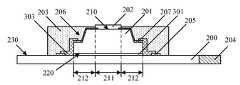
도 2를 참조한다. 본 발명의 실시 예에 따르면 지문 인식 칩의 패키지 구조는 회로기판(200), 센싱 칩 (201), 커버층 (202) 및 플라스틱 패키징 층(203)을 포함할 수 있다.See FIG. The package structure of the fingerprint recognition chip may include the
본 발명의 일 실시 예에 따르면 센싱 칩(201)은 회로기판(200)의 기판 표면에 결합될 수 있다. 센싱 칩(201)은 제1 표면 (210) 및 제1 표면 (210)에 대향하는 제2 표면 (220)을 포함할 수 있다. 센싱 칩 (201)의 제1 표면 (210)은 센싱 영역 (211)을 포함할 수 있다. 센싱 칩 (201)의 제2 표면(220)은 회로기판(200)의 기판 표면에 위치할 수 있다.According to an embodiment of the present invention, the
본 발명의 일 실시 예에 따르면 커버층(202)은 적어도 센싱 칩(201)의 센싱 영역(211)의 표면에 위치할 수 있다. 상기 실시 예에 따르면 커버층(202)은 폴리머로 이루어 질 수 있다.According to one embodiment of the present invention, the
본 발명의 일 실시 예에 따르면 플라스틱 패키징 층(203)은 회로기판(200)의 기판 표면 및 센싱 칩 (201)의 표면에 위치할 수 있다. 커버층 (202)은 플라스틱 패키징 층 (203)으로부터 노출될 수 있다.According to one embodiment of the present invention, the
이하, 지문 인식 칩의 패키지 구조에 대하여 상세하게 설명한다.Hereinafter, the package structure of the fingerprint recognition chip will be described in detail.
회로기판(200)은 센싱 칩(201)을 고정하고, 센싱 칩(201)을 다른 장치 또는 회로에 전기적으로 연결할 수 있다. 회로기판(200)은 센싱 칩(201)이 배치 될 장치 또는 단자에 따라 강성 회로기판 또는 플렉시블 회로기판일 수 있다. 본 발명의 일 실시 예에 따르면, 회로기판 (200)은 강성 회로기판일 수 있다. 강성 회로기판은 PCB 기판, 유리 기판, 금속 기판, 반도체 기판 또는 폴리머 기판일 수 있다.The
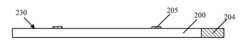
회로기판(200)의 회로기판 표면(230)을 포함할 수 있다. 센싱 칩(201)은 회로기판 (200)의 회로기판 표면(230)에 연결될 수 있다. 회로기판(200)의 회로기판 표면(230)에는 배선층(도시되지 않음)이 위치할 수 있으며, 회로기판(200)의 회로기판 표면(230)에 위치하는 제2 접속 단자(205)에 배선층이 접속될 수 있다. 제2 접속 단자(205)는 센싱 칩(201)의 표면에 위치한 칩 회로에 연결될 수 있다. 회로기판(200)은 센싱 칩(201)을 고정할 수 있으며, 센싱 칩(201)을 다른 장치 또는 회로에 전기적으로 연결할 수 있다. 회로기판(200)은 센싱 칩(201)이 설치될 장치 또는 단자에 따라 강성 회로기판 또는 플렉시블 회로기판일 수 있다. 본 발명의 일 실시 예에서, 회로기판 (200)은 강성 회로기판일 수 있다. 강성 회로기판은 PCB 기판, 유리 기판, 금속 기판, 반도체 기판 또는 폴리머 기판일 수 있다.And may include the
본 발명의 일 실시 예에 따르면, 회로기판(200)의 끝 단은 연결부(204)를 포함할 수 있다. 연결부(204)는 도전성 물질로 이루어질 수 있다. 연결부(204)는 외부 회로 또는 장치와 회로기판(200)의 회로기판 표면(230)의 배선층을 통해 연결될 수 있으며, 연결부(204)는 전기 신호를 전송할 수 있다.According to an embodiment of the present invention, the end of the
센싱칩(201)의 제1 표면(210)에 위치한 센싱 영역(211)은 사용자의 지문 정보를 감지하여 수신하도록 구성될 수 있다. 센싱 영역(211)에는 축전지 구조 또는 인덕터 구조가 제공 될 수 있으며, 축전지 구조 또는 인덕터 구조는 사용자의 지문 정보를 획득하도록 구성될 수 있다.The
본 발명의 일 실시 예에 따르면 적어도 하나의 평행판 축전지가 센싱 영역 (211)에 제공될 수 있다. 사용자의 손가락이 커버층(202)의 표면에 닿으면, 평행판 축전지, 커버층(202) 및 사용자의 손가락에 의해 축전지 구조가 형성될 수 있다. 센싱 영역(211)은 사용자의 손가락 표면의 돌출부와 평행판 축전지 사이의 정전용량 및 사용자의 손가락 표면의 함몰부와 평행판 축전지 사이의 정전용량을 획득할 수 있고, 칩 회로를 통하여 정전용량의 차이를 계산하고, 정전용량의 차이를 출력하여 사용자의 지문 데이터를 획득할 수 있다.According to one embodiment of the present invention, at least one parallel-plate battery may be provided in the
센싱칩(201)의 제1 표면(210)은 센싱 영역(211)을 둘러싸는 주변 영역(212)을 더 포함할 수 있다. 센싱칩(201)의 제1 표면(210)의 주변 영역(212)에는 칩 회로(미도시)가 제공될 수 있다. 칩 회로는 센싱 영역(211)의 축전지 구조 또는 인덕터 구조에 전기적으로 연결되며, 축전지 구조 또는 인덕터 구조에 의해 출력된 전기 신호를 처리할 수 있다.The
센싱 칩(201)은 주변 영역(212)에 위치한 에지 홈(206)을 더 포함할 수 있다. 에지 홈(206)은 센싱 칩(201)의 측벽으로부터 노출될 수 있다. 또한 센싱 칩(201)의 주변 영역(212)에 위치한 칩 회로는 에지 홈(206)의 바닥 표면 및 측벽의 표면 상에 위치할 수 있다. 에지 홈(206)의 바닥 표면에 위치하는 칩 회로의 일부는 제1 접속 단자(207)에 연결될 수 있다.The
에지 홈(206)은 칩 회로의 출력 단자, 즉 제1 접속 단자(207)를 형성하도록 구성된다. 회로기판(200)의 기판 표면에 제1 접속 단자(207)와 제2 접속 단자(205)를 전기적으로 연결함으로써, 센싱 칩(201)이 회로 기판(200)에 결합될 수 있다.The
본 발명의 일 실시 예에 따르면 에지 홈(206)은 센싱 영역(211)을 둘러싸는 연속적인 홈일 수 있다. 하나 이상의 제1 접속 단자(207)는 연속적인 에지 홈(206)의 바닥 표면에 제공될 수 있다. 본 발명의 다른 실시 예에 따르면 상기 에지 홈(206)는 상기 센싱 영역(211)을 둘러싸는 복수의 분리된 홈들을 포함할 수 있다. 하나 이상의 제1 접속 단자(207)는 개별적인 홈(206)이 각각 제공될 수 있다. 제1 접속 단자 (207)의 수 및 분포는 칩 회로의 특정 회로 레이아웃 요구조건에 기초하여 결정될 수 있다.According to one embodiment of the present invention, the
본 발명의 일 실시 예에 따르면, 에지 홈(206)의 측벽은 센싱 칩(201)의 표면에 대하여 경사져 있을 수 있다. 에지 홈(206)의 측벽과 바닥 표면 사이의 각은 둔각(obtuse angle)일 수 있다. 에지 홈(206)의 경사진 측벽의 표면은 칩 회로 및 센싱 영역(211)과 제1 연결 단자(207) 사이의 회로 레이아웃을 용이하게 형성할 수 있다.According to one embodiment of the present invention, the sidewalls of the
커버층(202)은 센싱 칩(201)의 센싱 영역(211)을 덮을 수 있다. 커버층(202)는 센싱 영역 (211)을 둘러싸는 주변 영역 (212)의 일부를 덮을 수도 있다. 커버층(202)은 폴리머로 이루어질 수 있다. 폴리머는 양호한 연성, 우수한 유연성 및 피복 성능을 가질 수 있다. 따라서, 커버층(202)은 두께가 얇고 경도가 높기 때문에 사용자의 지문을 감지하고 센싱 영역 (211)을 보호할 수 있는 커버층(202)의 용량을 확보하기 위하여 센싱 칩(201)의 용량을 향상시킬 수 있다.The
커버층(202)은 20 미크론 내지 100 미크론 범위의 두께를 가질 수 있다. 커버층(202)의 두께는 작을 수 있다. 사용하는 손가락이 커버층(202)의 표면에 닿을 때, 손가락과 센싱 영역(211) 사이의 거리는 감소된다. 따라서, 센싱 영역(211)에 의해 사용자의 지문을 보다 쉽게 감지할 수 있어 센싱 칩(201)의 감도에 대한 요구를 줄일 수 있다.The
본 발명의 일 실시 예에 따르면 평행판 축전지는 센싱 영역 (211)에 위치할 수 있다. 커버층(202)의 두께가 얇기 때문에 사용자의 손가락과 평행판 축전지 사이의 거리가 감소될 수 있다. 그 결과, 사용자의 손가락과 평행판 축전지 사이의 정전용량은 작아질 수 있으며. 따라서 사용자의 손가락 표면의 돌출부와 평행판 축전지 사이의 정전용량과 함몰부와 평행판 축전지 사이의 정전용량 사이의 차이는 커질 수 있으며, 이에 따라 센싱 영역(211)은 사용자의 지문정보를 쉽게 획득 할 수 있다.According to one embodiment of the present invention, the parallel plate battery may be located in the
커버층(202)은 8H 이상인 모스 경도를 가질 수 있다. 커버층 (202)의 경도는 높을 수 있다. 따라서, 커버층(202)의 두께가 얇더라도 커버 층(202)은 센싱 칩(201)의 센싱 영역(211)을 보호 할 수 있으며, 센싱 칩(201)은 사용자의 손가락이 커버층(202)의 표면위로 움직일 때 손상을 받지 아니할 수 있다. 또한, 커버층(202)의 경도가 높기 때문에, 커버층(202)에 변형이 발생하기 어렵다. 사용자의 손가락이 커버층 (202)의 표면에 압력을 주더라도, 커버층(202)의 두께는 거의 변화하지 않으므로, 센싱 영역(211)의 검출 결과의 정확성이 보장될 수 있다.The
본 발명의 일 실시 예에 따르면 커버층(202)은 7 이상의 유전 상수를 가질 수 있다. 커버층(202)의 전기적 절연 용량은 크다. 따라서, 센싱 영역(211)을 보호하기 위한 커버층 (202)의 용량은 클 수 있다.According to an embodiment of the present invention, the
본 발명의 일 실시 예에 따르면 커버층(202)의 두께는 얇을 수 있으며, 사용자의 손가락과 평행판 축전기 사이의 정전용량은 커버층(202)의 두께에 반비례하며, 유전 상수에 비례할 수 있다. 따라서, 커버층(202)의 두께가 얇고 유전율이 크면 사용자의 손가락과 평행판 축전기 사이의 정전용량은 센싱 영역(211)에서 감지 할 수 있는 범위 내에 있을 수 있으므로, 정전용량이 너무 크거나 작아서 센싱 영역(211)의 탐색을 실패하는 것을 회피할 수 있다.According to one embodiment of the present invention, the thickness of the
또한, 커버층(202)의 두께가 20~100 미크론이고 유전율이 7 이상인 경우에, 커버 층(202)의 유전율은 커버층(202)의 두께가 증가함에 따라 증가하기 때문에, 센싱 영역(211)에 의해 검출 가능한 안정된 범위 내에서 사용자의 손가락과 평행판 축전기 사이의 정전용량을 안정화시킬 수 있다.In addition, since the dielectric constant of the
본 발명의 일 실시 예에 따르면 커버층(202)은 에폭시 수지(epoxy resin), 폴리미드 수지(polyimide resin), 벤조사이클로뷰텐 수지(polybenzoxazole resin), 폴리벤즈옥사졸 수지(Polybenzoxazole resin), 폴리부틸렌테레프탈레이드(polybutylene terephthalate), 폴리카보네이트(polycarbonate), 폴리에틸렌테레프탈레이트(polyethylene terephthalate), 폴리에틸렌(polyethylene), 폴리프로필렌(polypropylene), 폴리올레핀(polyolefin), 폴리우레탄(polyurethane), 폴리올레핀(polyolefin), 폴리에테르술폰(polyethersulfone), 폴리아미드(polyamide), 폴리 우레탄(polyurethane), 에틸렌초산비닐 공중합체(ethylene-vinyl acetate copolymer), 폴리비닐 알코올(polyvinyl alcohol)또는 적합한 폴리머로 이루어질 수 있다.According to an embodiment of the present invention, the
본 발명의 일 실시 예에 따르면 폴리머는 감광성 재료로 만들어 질 수 있다. 감광성 입자는 폴리머 내에 제공되고, 감광성 입자와 함께 폴리머는 노광 및 현상되어 패턴을 형성 할 수 있다. 감광성 입자는 6 미크론보다 작은 크기를 가지므로, 폴리머를 노출시킴으로써 형성된 커버층(202)의 크기는 정확하고 쉽게 제어할 수 있다.According to one embodiment of the present invention, the polymer may be made of a photosensitive material. Photosensitive particles are provided in the polymer, and the polymer together with the photosensitive particles can be exposed and developed to form a pattern. Since the photosensitive particles have a size of less than 6 microns, the size of the
본 발명의 일 실시 예에 따르면 지문 인식 칩 패키지는 도전성 와이어 (208)를 더 포함할 수 있다. 도전선(208)의 양 끝단은 제1 접속 단자(207) 및 제2 접속 단자(205)에 각각 접속되어 칩 회로와 회로 기판(200)의 기판 표면상 배선층(wiring layer)을 전기적으로 접속 할 수 있다. 배선층은 연결부(204)와 전기적으로 접속될 수 있으며, 센싱 칩(201)의 표면의 칩 회로와 센싱 영역 (211)은 외부 회로 또는 장치와 전기 신호를 송수신할 수 있다. 도전성 와이어(208)는 구리, 텅스텐, 알루미늄, 금 또는 은과 같은 금속으로 만들어질 수 있다.According to an embodiment of the present invention, the fingerprint recognition chip package may further include the
본 발명의 일 실시 예에 따르면 지문 인식 칩의 패키지 구조는 도전성 와이어(208)를 통해 제1 접속 단자(207)와 제2 접속 단자(205)가 접속 됨으로써 지문 인식 칩의 패키지 구조는 센싱 칩(201)과 회로 기판(200) 사이에 위치하는 제1 본딩층(301)을 더 포함할 수 있다. 상기 본딩층(301)은 회로 기판(200)의 기판 표면(230)위에 센싱 칩(201)을 고정할 수 있다.According to an embodiment of the present invention, the package structure of the fingerprint recognition chip is such that the
본 발명의 일 실시 예에 따르면 지문 인식 칩의 패키지 구조는 회로 기판(200)의 기판 표면 위에 위치하는 보호링(209)을 더 포함할 수 있다. 보호링(209)은 센싱 칩(201), 커버층(202) 및 플라스틱 패키징 층(203)을 둘러쌀 수 있다. 보호링 (209)은 금속으로 이루어질 수 있다. 보호링(209)은 회로 기판(200)을 통해 접지될 수 있다. 보호링(209)은 회로 기판(200)의 기판 표면(230)위에 고정될 수 있다.According to an embodiment of the present invention, the package structure of the fingerprint recognition chip may further include a
본 발명의 일 실시 예에 따르면 보호링(209)은 센싱 칩(201), 커버층(202) 및 플라스틱 패키징 층(203) 주위에 위치할 수 있으며 플라스틱 패키징 층(203)의 일부분을 덮을 수 있으며, 커버층(202)의 표면은 보호링으로부터 노출될 수 있다. 또 다른 실시 예에 따르면 보호링은 센싱 칩(201) 및 플라스틱 패키징 층(203) 주위에만 위치될 수 있으며, 플라스틱 패키징 층(203)의 표면 및 커버층(202)의 표면은 보호링으로부터 노출될 수 있다.According to one embodiment of the present invention, the
보호링(209)은 구리, 텅스텐, 알루미늄, 금 또는 은과 같은 금속으로 제조될 수 있다. 보호링 (209)은 센싱 칩에 대해 정전기 보호를 제공할 수 있다. 보호링 (209)은 금속으로 이루어져 있기 때문에, 보호링 (209)은 도전성을 갖는다. 사용자의 손가락이 커버층(202)에 닿으면 정전기가 발생할 수 있고, 보호링(209)을 통해 회로 기판(200)으로 정전기(electrostatic)가 전달될 수 있고, 이로 인하여 정전기 전압(electrostatic voltage)이 너무 커서 파손되는 것으로부터 커버층(202)을 보호할 수 있다. 이러한 방식으로, 센싱 칩(201)이 보호되고, 지문 검출의 정확성이 향상될 수 있다. 센싱 칩이 출력하는 신호 잡음이 제거되어 센싱 칩이 출력하는 신호가 더욱 정확해질 수 있다.The
본 발명의 일 실시 예에 따르면 도 3에 도시 된 바와 같이 지문 인식 칩의 패키지 구조는 센싱 칩(201)의 측벽 표면, 회로 기판(200)의 제1 표면 (210) 및 에지 홈(206)을 가질 수 있다. 센싱 영역(211)과 회로 기판(200)의 기판 표면상의 배선층과의 전기적 접속을 달성하기 위해, 도전층 (303)의 양 끝단은 제 1 접속 단자 (207) 및 제 2 접속 단자 (205) 및 회로 기판(200)의 기판 표면에 배선층을 포함할 수 있다. 지문 인식 칩의 패키지 구조는 센싱 칩 (201)과 회로 기판(200)사이에 위치하는 제 1 본딩층(301)을 더 포함할 수 있다.3, the package structure of the fingerprint recognition chip includes a side wall surface of the
본 발명의 또 다른 실시 예에 따르면 도 4에 도시 된 바와 같이 센싱 칩(201)은 센싱 칩(201)을 통해 연장되는 도전성 플러그(conductive plug)(304)를 더 포함할 수 있다. 도전성 플러그 (304)는 센싱 칩(201)의 제2 표면(220)으로부터 노출될 수 있다. 도전성 플러그 (304)의 한쪽 끝단은 제1 접속 단자 (207)에 연결될 수 있다. 센싱 칩(201)은 센싱 칩(201)의 제2 표면 (220)으로부터 노출된 도전성 플러그(304)의 상단에 위치한 땜납층(solder layer)(305)을 더 포함할 수 있다. 센싱 영역(211)과 회로 기판(200)의 기판 표면 상의 배선층 사이와 칩 회로 및 회로 기판(200)의 기판 표면 상의 배선층의 사이에 전기적인 연결을 달성하기 위하여 땜납층(305)은 제2 접속 단자(205)의 표면에 용접될 수 있다. 센싱 칩 (201)은 땜납층 (305)을 통해 회로 기판(200)의 기판 표면(230)에 용접되므로, 센싱 칩(201)은 회로 기판(200)에 고정될 수 있다.According to another embodiment of the present invention, as shown in FIG. 4, the
본 발명의 일 실시 예에 따르면 도 5에 도시 된 바와 같이, 지문 인식 칩의 패키지 구조는 플라스틱 패키징 층(203), 센싱 칩(201) 및 보호링 (209)을 둘러싸는 하우징(400)을 더 포함할 수 있다. 커버층(202)은 하우징(400)으로부터 노출될 수 있으며, 이로 인하여 지문을 검출하기 위하여 사용자의 손가락을 이용하여 커버층(202)의 표면과 접촉될 수 있다. 커버 층(202)의 색은 하우징(400)의 색상과 동일할 수 있다. 예를 들어, 하우징 (400)이 흑색이면, 커버층(202)은 흑색이고; 하우징(400)이 백색 인 경우, 커버 층(202)은 백색일 수 있다. 이와 같이, 지문 인식 칩의 패키지 구조는 전체적으로 조화로운 외관을 가질 수 있다.5, the package structure of the fingerprint recognition chip includes a
본 발명의 또 다른 실시 예에 따르면 도 6에 도시 된 바와 같이 지문 인식 칩의 패키지 구조는 보호링(209)을 포함하지 않을 수 있으며, 지문 인식 칩의 패키지 구조는 플라스틱 패키징 층(203) 및 센싱 칩(201)을 둘러싸는 하우징을 포함할 수 있다. 커버층(202)은 하우징(400)으로부터 노출될 수 있다. 커버 층 (202)의 색상은 하우징 (400)의 색상과 동일할 수 있다.6, the package structure of the fingerprint recognition chip may not include the
본 발명의 일 실시 예에 따르면 센싱 칩의 제2 표면은 회로 기판의 기판 표면에 결합될 수 있으며, 센싱 칩의 제 1 표면은 센싱 영역을 포함하고 센싱 영역은 사용자의 지문을 추출할 수 있다. 커버층은 센싱 칩의 센싱 영역의 표면에 위치할 수 있으며, 커버층은 센싱 칩의 센싱 영역을 보호할 수 있으며, 센싱 영역은 커버층의 표면에 사용자의 손가락이 닿을 때 사용자의 지문을 추출할 수 있고, 센싱 칩은 사용자의 지문을 전기 신호로 변환하여 전기 신호를 출력할 수 있다. 커버층은 폴리머로 이루어질 수 있다. 폴리머는 우수한 연성, 유연성 및 우수한 피복 성능을 가지므로, 커버층의 두께가 얇고, 센싱 칩을 보호하기에 충분한 경도를 가질 수 있다. 또한, 커버층 표면과 센싱 칩 사이의 거리가 줄어들어 센싱 칩이 사용자의 지문을 쉽게 감지 할 수 있다. 따라서, 이러한 패키지 구조는 센싱 칩의 감도에 대한 요구가 감소할 수 있으며, 지문 인식 칩의 패키지 구조가 보다 광범위하게 적용될 수 있다. 또한, 커버층이 폴리머로 이루어질 수 있기 때문에, 커버층의 저비용화가 가능해져, 패키지 구조의 제조 비용을 절감할 수 있다.According to an embodiment of the present invention, the second surface of the sensing chip may be coupled to the substrate surface of the circuit board, the first surface of the sensing chip may include a sensing region, and the sensing region may extract a fingerprint of the user. The cover layer can be located on the surface of the sensing area of the sensing chip, the cover layer can protect the sensing area of the sensing chip, and the sensing area can extract the fingerprint of the user when the user's finger touches the surface of the cover layer And the sensing chip can convert the fingerprint of the user into an electric signal and output an electric signal. The cover layer may be made of a polymer. Since the polymer has excellent ductility, flexibility and excellent coating performance, the thickness of the cover layer is thin, and it can have sufficient hardness to protect the sensing chip. In addition, the distance between the surface of the cover layer and the sensing chip is reduced, so that the sensing chip can easily sense the fingerprint of the user. Therefore, such a package structure can reduce the sensitivity of the sensing chip, and the package structure of the fingerprint recognition chip can be applied more widely. Further, since the cover layer can be made of a polymer, it is possible to reduce the cost of the cover layer, and the manufacturing cost of the package structure can be reduced.
이에 대응하여, 도 7 내지 도 12에 도시 된 바와 같이 본 발명의 일 실시 예에 따라 상술된 지문 인식 칩의 패키지 구조를 형성하기 위한 패키징 방법이 더 제공된다.Correspondingly, as shown in FIGS. 7 to 12, a packaging method for forming the package structure of the above-described fingerprint recognition chip according to an embodiment of the present invention is further provided.
도 7에 도시 된 바와 같이, 회로기판(200)이 제공될 수 있다.As shown in Fig. 7, a
회로 기판(200)은 센싱 칩(201)이 배치될 장치 또는 단자에 따라 강성 회로기판 또는 플렉시블 회로기판일 수 있다. 본 발명의 일 실시 예에 따르면, 회로기판 (200)은 강성 회로기판일 수 있다. 강성 회로기판은 PCB 기판, 유리 기판, 금속 기판, 반도체 기판 또는 폴리머 기판일 수 있다.The
회로 기판(200)은 기판 표면(230)을 포함할 수 있다. 그 후에 형성된 센서 칩은 기판 표면(230)에 결합될 수 있다. 배선층 및 제2 접속 단자(205)는 회로 기판(200)의 기판 표면(230)에 형성될 수 있다. 배선층은 제2 접속 단자(205)에 접속될 수 있다.The
본 발명의 일 실시 예에 따르면 회로 기판 (200)의 한 쪽 끝단에 연결부(204)가 형성될 수 있다. 연결 (204)는 도전성 물질로 이루어질 수 있다. 배선층은 연결부(204)에 접속될 수 있으며, 이로 인하여 배선층 및 제2 접속 단자는 외부 회로 또는 디바이스에 전기적으로 접속될 수 있다.According to an embodiment of the present invention, a connecting
도 8에 도시된 바와 같이, 센싱 칩(201)은 회로 기판(200)의 기판 표면(230)에 고정될 수 있다. 센싱 칩(201)은 제1 표면 (210) 및 제1 표면(210)에 대향하는 제2 표면(220)을 포함할 수 있다. 센싱 칩 (201)의 제1 표면(210)은 센싱 영역(211)을 포함할 수 있다. 센싱 칩(201)의 제2 표면(220)은 회로 기판(200)의 기판 표면에 위치할 수 있다.As shown in FIG. 8, the
센싱 영역(211)은 사용자의 지문 정보를 감지하여 수신할 수 있다. 축전지 구조 또는 인덕터 구조는 센싱 영역(211)에 제공 될 수 있다. 축전지 구조 또는 인덕터 구조는 사용자의 지문 정보를 획득하도록 구성될 수 있다.The
센싱 영역(211)은 사용자의 손가락 표면의 돌출부와 평행판 축전기 사이의 정전용량과 사용자의 손가락 표면의 함몰부와 평행판 축전기 사이의 정전용량과의 차이를 구할 수 있으며, 칩 회로를 통해 상기 정전용량들의 차이를 구할 수 있으며, 상기 정전용량들의 차이를 출력하여 사용자의 지문 데이터를 획득할 수 있다.The
센싱 칩(201)은 센싱 영역(211)을 둘러싸는 주변 영역(212)을 더 포함할 수 있다. 센싱 칩(201)의 주변 영역(212)에 에지 홈(206)이 형성될 수 있다. 홈 (206)은 센싱 칩 (201)의 측벽으로부터 노출될 수 있다. 제1 접속 단자(207)는 홈(206)의 하단에 형성될 수 있다. 칩 회로는 센싱 칩(201)의 제1 표면(210)에 형성될 수 있다. 칩 회로는 홈(206)의 내부로 연장될 수 있으며, 제1 접속 단자(207)에 접속될 수 있다. 제1 접속 단자(207)는 칩 회로의 출력 단자일 수 있다.The
본 발명의 일 실시 예에 따르면 에지 홈(206)은 센싱 영역(211)을 둘러싸는 연속적인 홈일 수 있다. 연속적인 에지 홈(206)의 바닥 표면에는 하나 이상의 제1 접속 단자(207)가 형성될 수 있다. 본 발명의 또 다른 실시 예에 따르면 에지 홈(206)은 센싱 영역(211)을 둘러싸는 복수의 별개의 홈들을 포함할 수 있다. 하나 이상의 제1 연결 단자들(207)은 별개의 에지 홈들(206)에 각각에 형성될 수 있다.According to one embodiment of the present invention, the
본 발명의 일 실시 예에 따르면 에지 홈(206)의 측벽은 센싱 칩(201)의 표면에 대해 경사져 있을 수 있다. 측벽과 에지 홈(206)의 바닥 사이의 각도는 둔각일 수 있다. 에지 홈(206)에 칩 회로가 형성될 경우에는 칩 회로의 레이아웃 형성을 위해 칩 회로의 재료로 포토리소그래피 (photolithography) 및 에칭(etching) 프로세스를 수행하여 경사진 측벽의 표면을 형성하는 것이 용이하다.According to an embodiment of the present invention, the sidewalls of the
본 발명의 일 실시 예에 따르면 센싱 칩은 제1 본딩층(301)을 통해 회로 기판(200)의 기판 표면(230)에 고정될 수 있다. 이어서, 제1 접속 단자(207)는 도전성 와이어 또는 도전층을 통해 제2 접속 단자(205)에 접속될 수 있다.According to an embodiment of the present invention, the sensing chip may be fixed to the
본 발명의 또 다른 실시 예에 따르면 도 4에 도시 된 바와 같이, 센싱 칩(201)을 관통하여 연장되는 도전성 플러그(304)가 센싱 칩(201)에 형성될 수 있다. 도전성 플러그(304)는 센싱 칩(201)의 제2 표면(220)으로부터 노출될 수 있다. 도전성 플러그(304)의 한쪽 끝단은 제1 접속 단자(207)에 접속될 수 있다. 센싱 칩(201)의 제2 표면(220)으로부터 노출된 도전성 플러그 (304)의 상단에는 땜납층(305)이 형성될 수 있다. 땜납층(305)은 제2 연결 단자(205)의 표면에 용접될 수 있으며, 센싱 칩(201)과 회로 기판(200)을 서로 고정시킬 수 있다.According to another embodiment of the present invention, as shown in FIG. 4, a
도 9에 도시 된 바와 같이, 코팅 공정을 통해 회로 기판(200)의 기판 표면과 센싱 칩(201)의 표면에 커버 필름(202a)이 형성될 수 있다. 커버 필름(202a)은 폴리머로 이루어질 수 있다.As shown in FIG. 9, a
커버 필름 (202a)은 이후에 커버층을 형성하도록 구성될 수 있다. 폴리머는 우수한 연성, 유연성 및 유동성을 가지고 있으며 높은 피복 성능을 가지고 있다. 따라서, 두께가 얇은 커버 필름 (202a)은 코팅 공정을 통해 센싱 영역 (211)의 표면에 형성될 수 있으며, 그 결과 이후에 센싱 영역(211)의 표면에 형성될 커버층의 두께가 얇아질 수 있다. 커버층의 두께가 얇으면, 사용자의 지문을 감지하기 위한 센싱 칩(201)의 수용력(capacity)이 향상되고 그에 따라 센싱 칩(201)의 감지 감도에 대한 요구도 낮아질 수 있다.The
코팅 공정은 스핀 코팅 공정(spin coating process), 스프레이 코팅 공정(spray coating process) 또는 증발 공정(evaporation process)을 포함할 수 있다. 커버 필름(202a)을 형성하기 위한 재료가 유체이기 때문에, 회로 기판(200)의 기판 표면의 커버 필름(202a)은 큰 두께를 가지는 반면에 센서 칩(201)의 표면에 형성된 커버 필름 (202a)은 얇은 두께를 가질 수 있다. 센싱 칩(201)의 표면에 형성된 커버 필름 (202a)의 두께는 20 ~ 100 미크론일 수 있다.The coating process may include a spin coating process, a spray coating process, or an evaporation process. The
커버 필름(202a)은 에폭시 수지(epoxy resin), 폴리미드 수지(polyimide resin), 벤조사이클로뷰텐 수지(benzocyclobutene resin), 폴리벤즈옥사졸 수지(Polybenzoxazole resin),폴리부틸렌테레프탈레이드(polybutylene terephthalate), 폴리카보네이트(polycarbonate), 폴리에틸렌테레프탈레이트(polyethylene terephthalate), 폴리에틸렌(polyethylene), 폴리프로필렌(polypropylene), 폴리올레핀(polyolefin), 폴리우레탄(polyurethane), 폴리올레핀(polyolefin), 폴리에테르술폰polyethersulfone), 폴리아미드(polyamide), 폴리 우레탄(polyurethane), 에틸렌초산비닐 공중합체(ethylene-vinyl acetate copolymer), 폴리비닐 알코올(polyvinyl alcohol)또는 적합한 폴리머로 이루어질 수 있다.The
본 발명의 일 실시 예에 따르면 폴리머는 감광성 재료로 이루어 질 수 잇다. 감광성 입자는 폴리머 내에서 제공될 수 있으며, 감광성 입자와 함께 폴리머는 노광 및 현상될 수 있다. 따라서, 커버층 (202a)을 직접 노광함으로써 커버층을 형성 할 수 있다. 감광성 입자는 6 미크론보다 작은 크기를 가지므로, 노광에 의해 후속적으로 형성되는 커버층(202)의 크기를 더 정밀하고 쉽게 제어할 수 있다.According to one embodiment of the present invention, the polymer may be made of a photosensitive material. Photosensitive particles may be provided in the polymer and the polymer may be exposed and developed with the photosensitive particles. Therefore, the cover layer can be formed by directly exposing the
도 10에 도시 된 바와 같이, 센싱 영역(211)의 표면에 커버층 (202)을 형성하기 위하여 회로 기판(200)의 기판 표면 및 센싱 영역(211)아닌 센싱 칩(201)의 제1 표면의 다른 부분(도 9에 도시 된 바와 같이)의 커버 필름 (202a)을 제거할 수 있다 (도 9에 도시 된 바와 같이).10, in order to form the
본 발명의 일 실시 예에 따르면 커버 필름 (202a)을 형성하기 위한 폴리머는 감광성 재료로 이루어질 수 있으며, 이로 인하여 노광 및 현상 공정을 통해 센싱 영역(211)이외의 커버 필름(202a)을 제거하여 커버층(202)을 형성할 수 있다. 또한, 노광 및 현상 후, 형성된 커버층(202)에 응고 공정(solidification process)을 실시하여 커버층(202)의 재료를 고화시킬 수 있다. 형성된 커버층(202)은 센싱 영역(211)의 표면을 덮을 뿐만 아니라, 센싱 영역(211)을 둘러싸는 주변 영역(212)의 부분도 덮을 수 있다.According to one embodiment of the present invention, the polymer for forming the
본 발명의 또 다른 실시 예에 따르면 커버층(202)을 형성하는 공정은 커버 필름(202a)의 표면에 마스크 층을 형성하는 단계, 상기 마스크 층은 커버층(202)응 형성하기 위한 대응 위치 및 패턴으로 정의될 수 있으며; 커버층(202)을 형성하기 위하여 회로 기판(200)의 기판 표면과 센싱 칩(201)의 표면이 노출될 때까지 마스크 층을 마스크로하여 커버 필름(202a)을 에칭(etching)하는 단계를 포함할 수 있다.According to another embodiment of the present invention, the process of forming the
커버층(202)은 20 미크론에서 100 미크론의 두께를 가지므로, 센싱 영역(211)이 사용자의 손가락의 지문 정보를 용이하게 검출할 수 있다.Since the
응고 공정(solidification process) 후에, 커버 필름(202a)은 8H 이상의 모스 경도를 가질 수 있다. 커버층(202)의 경도가 높기 때문에, 사용자의 손가락이 커버층(202)의 표면에서 움직이는 경우에도 센싱 칩 (201)은 손상되지 아니한다. 또한, 커버층(202)의 경도가 높기 때문에, 커버층(202)에 변형이 생기기 어렵다. 사용자의 손가락이 커버층(202)의 표면을 눌러도, 커버 층(202)의 두께의 변화는 거의 생기지 아니한다. 이로 인하여 센싱 영역(211)의 검출 결과에 대한 정밀도가 확보될 수 있다.After the solidification process, the
커버층(202)은 7 이상의 유전 상수를 가질 수 있다. 커버층(202)의 전기 절연 용량(Electrical isolation capacity)은 클 수 있다. 따라서, 센싱 영역(211)을 보호하기 위한 커버층(202)의 수용력(of the cover layer)은 클 수 있다. 또한, 본 발명이 일 실시 예에 따르면 커버층(202)의 두께가 얇고 유전율이 클 경우, 사용자의 손가락과 평행판 축전기 사이의 정전용량은 센싱 영역(211)에 의해 검출 가능한 범위 내에 있을 수 있으므로, 감지 실패를 회피할 수 있다.The
도 11에 도시 된 바와 같이, 커버층(202)이 형성된 후에, 회로 기판(200)은 센싱 칩(201)에 결합될 수 있다.As shown in FIG. 11, after the
본 발명의 일 실시 예에 따르면 센싱 칩(201)은 제1 본딩층(301)을 통해 회로 기판(200)의 기판 표면에 고정될 수 있으며, 회로 기판(200)은 도전성 와이어 또는 도전 층을 통해 센싱 칩(201)에 결합 될 수 있다.According to an embodiment of the present invention, the
본 발명의 일 실시 예에 따르면 센싱 칩(201)을 회로 기판(200)의 기판 표면에 결합시키는 과정에서 도전성 와이어(208)를 제공하고, 도전성 와이어 (208)의 양 끝단을 제1 연결 단자(207) 및 제2 연결 단자(205)에 용접을 통하여 연결하는 것을 포함할 수 있다. 도전성 와이어(208)는 구리, 텅스텐, 알루미늄, 금 또는 은과 같은 금속으로 이루어질 수 있다.According to an embodiment of the present invention, a
본 발명의 일 실시 예에 따르면 도 3에 도시 된 바와 같이, 센싱 칩(201)을 회로 기판(200)의 기판 표면에 결합시키는 공정은 회로 기판(200)의 기판 표면,센싱 칩(201)의 측벽의 표면, 에지 홈 내부에 도전층(303)을 형성하는 단계를 포함할 수 있다. 도전층(303)의 양 끝단은 제1 접속 단자(207) 및 제2 접속 단자(205)에 각각 연결될 수 있다. 도전층 (303)을 형성하는 공정은 증착 공정(deposition process), 도금 공정(plating process) 또는 화학 도금 공정(chemical plating process)를 포함할 수 있으며 도전 필름의 일부분을 에칭하여 도전층(303)을 형성할 수 있다. 도전층(303)은 구리, 텅스텐, 알루미늄, 은, 금, 티탄(titanium), 탄탈(tantalum), 니켈(nickel), 질화티탄 (titanium nitride), 질화탄탈(tantalum nitride )또는 이들의 임의의 조합과 같은 금속으로 이루어 질 수 있다.3, the process of bonding the
도 12에 도시 된 바와 같이, 플라스틱 패키징 층(203)은 회로 기판(200)의 기판 표면 및 센싱 칩(201)의 표면에 형성될 수 있으며. 커버층(202)은 플라스틱 패키징 층(203)으로부터 노출될 수 있다.12, a
플라스틱 패키징 층(203)은 에폭시 수지, 폴리에틸렌, 폴리 프로필렌, 폴리올레핀, 폴리 아미드, 폴리 우레탄 또는 다른 적절한 성형 재료로 제조될 수 있다. 플라스틱 패키징 층(203)을 형성하는 공정은 사출 성형 공정(injection molding process), 트랜스퍼 성형 공정(transfer molding process), 스크린 인쇄 공정(screen printing process) 또는 다른 적절한 공정을 포함할 수 있다.The
본 발명의 일 실시 예에 따르면 도 2에 도시 된 바와 같이, 플라스틱 패키징 층(203)이 형성된 후에, 보호링(209)이 회로 기판(200)의 기판 표면에 형성될 수 있다. 보호 링(209)은 센싱 칩(201), 커버층(202) 플라스틱 패키징 층을 둘러쌀 수 있다. 보호 링(209)은 금속으로 이루어질 수 있다. 보호 링 (209)은 기판 (200)을 통해 접지된다. 보호링(209)은 구리, 텅스텐, 알루미늄, 금 또는 은과 같은 금속으로 이루어질 수 있다.According to one embodiment of the present invention, as shown in FIG. 2, after the
보호링(209)은 너무 큰 정전 전압(electrostatic voltage)으로 인해 커버층(202)이 고장 나버리는 것을 보호하기 위하여 센싱 칩에 정전기 보호를 제공할 수 있다. 이러한 방식으로 센싱 칩(201)은 보호될 수 있으며, 지문 검출의 정확성이 향상될 수 있다. 센싱 칩이 출력하는 신호 잡음이 제거되어 센싱 칩이 출력하는 신호가 더욱 정확해질 수 있다.The
본 발명의 일 실시 예에 따르면 센싱 칩의 제1 표면은 사용자의 지문을 추출하도록 구성된 센싱 영역을 포함할 수 있으며, 센싱 칩의 센싱 영역의 표면에 커버층이 형성될 수 있고, 센싱 칩의 센싱 영역을 보호하도록 커버층이 구성될 수 있으며, 커버층의 표면은 사용자의 손가락의 지문을 검출을 위해 사용될 수 있다. 커버층은 폴리머로 이루어 질 수 있다. 폴리머는 우수한 연성, 유연성 및 우수한 피복 성능을 가질 수 있으며, 형성된 커버층의 두께가 얇고, 센싱 칩을 보호하기에 충분한 경도를 가질 수 있다. 또한, 커버층의 표면과 센싱 칩 사이의 거리가 감소되어 센싱 영역이 사용자의 지문 데이터를 쉽게 감지할 수 있다. 따라서, 형성된 패키지 구조는 센싱 칩의 감도에 대한 요구가 감소됨으로써 패키지 방법이 보다 광범위하게 적용될 수 있다. 또한, 커버층이 폴리머로 구성되어 있기 때문에, 커버층의 저비용화가 가능해져, 패키지 구조의 제조 비용을 저감 할 수 있다.According to an embodiment of the present invention, the first surface of the sensing chip may include a sensing area configured to extract a fingerprint of a user, a cover layer may be formed on a surface of the sensing area of the sensing chip, A cover layer can be constructed to protect the area, and the surface of the cover layer can be used for detecting the fingerprint of the user's finger. The cover layer may be made of a polymer. The polymer may have excellent ductility, flexibility and good coating performance, and the formed cover layer may be thin and of sufficient hardness to protect the sensing chip. In addition, the distance between the surface of the cover layer and the sensing chip is reduced, so that the sensing area can easily sense the user's fingerprint data. Thus, the formed package structure can be applied to a wider range of packaging methods by reducing the need for sensitivity of the sensing chip. Further, since the cover layer is made of a polymer, it is possible to reduce the cost of the cover layer, and the manufacturing cost of the package structure can be reduced.
본 발명은 상술한 설명에 의해 개시되지만, 이에 한정되지 아니한다. 당업자는 본 발명의 사상 및 범위를 벗어나지 않고 다양한 변경 및 변형을 수행할 수 있다. 그러므로, 본 개시의 범위는 청구 범위에 의해 한정된다.The present invention is disclosed by way of the above description, but is not limited thereto. Those skilled in the art can make various changes and modifications without departing from the spirit and scope of the invention. Therefore, the scope of the present disclosure is defined by the claims.
Claims (20)
Translated fromKorean회로기판 표면을 포함하는 회로기판;
상기 회로기판 표면에 결합된 센싱 칩, 상기 센싱 칩은 제1 표면 및 상기 제 1 표면에 대향하는 제2 표면을 포함하며, 상기 센싱 칩의 제1 표면은 센싱 영역을 포함하고, 상기 센싱 칩의 제2 표면은 회로기판 표면에 위치하며;
적어도 상기 센싱 칩의 센싱 영역의 표면에 위치하는 커버층, 상기 커버 층은 폴리머로 이루어지고; 및
상기 회로기판 표면 및 상기 센싱 칩의 제 1 표면에 위치한 플라스틱 포장 층, 상기 커버 층은 상기 플라스틱 포장 층으로부터 노출되어있는 것을 특징으로 하는 지문 인식 칩의 패키지 구조.In a package structure of a fingerprint recognition chip,
A circuit board including a circuit board surface;
A sensing chip coupled to the surface of the circuit board, the sensing chip including a first surface and a second surface opposite the first surface, the first surface of the sensing chip including a sensing area, The second surface is located on the circuit board surface;
A cover layer located at least on a surface of the sensing region of the sensing chip, the cover layer being made of a polymer; And
A plastic packaging layer located on the surface of the circuit board and a first surface of the sensing chip; and the cover layer is exposed from the plastic packaging layer.
상기 커버 층의 두께는 20 ㎛ 이상 100 ㎛ 이하이고, 상기 커버 층의 모스 경도는 8H 이상이며, 상기 커버 층의 유전 상수는 7보다 크거나 같은 것을 특징으로 하는 지문 인식 칩의 패키지 구조.The method according to claim 1,
Wherein a thickness of the cover layer is 20 占 퐉 or more and 100 占 퐉 or less, a Mohs hardness of the cover layer is 8H or more, and a dielectric constant of the cover layer is greater than or equal to 7.
상기 폴리머는 감광성 재료로 이루어지는 것을 특징으로 하는 지문 인식 칩의 패키지 구조.The method according to claim 1,
Wherein the polymer is made of a photosensitive material.
상기 감광성 입자는 상기 커버 층에 제공되고, 상기 감광성 입자는 6 미크론 미만의 크기를 갖는 것을 특징으로 하는 지문 인식 칩의 패키지 구조.The method of claim 3,
Wherein the photosensitive particles are provided in the cover layer, and the photosensitive particles have a size of less than 6 microns.
상기 센싱 칩의 제1 표면은 상기 센싱 영역을 둘러싸는 주변 영역을 더 포함하는 것을 특징으로 하는 지문 인식 칩의 패키지 구조.The method according to claim 1,
Wherein the first surface of the sensing chip further includes a peripheral region surrounding the sensing region.
에지 홈은 상기 주변 영역에 위치하며, 상기 에지 홈은 센싱 칩의 측벽으로부터 노출되고; 및
칩 회로는 상기 센싱 칩의 주변 영역 상에 위치하며, 상기 칩 회로는 상기 센싱 칩의 주변 영역의 표면 및 상기 에지 홈의 측벽 및 바닥 표면에 위치하고, 상기 에지 홈의 바닥에 위치하는 상기 칩 회로의 일부분이 제1 접속 단자를 포함하는 것을 특징으로 하는 지문 인식 칩의 패키지 구조.The method of claim 5,
Edge grooves are located in the peripheral region, and the edge grooves are exposed from the side walls of the sensing chip; And
Wherein the chip circuit is located on a peripheral region of the sensing chip, the chip circuit being located on a surface of a peripheral region of the sensing chip and on a side wall and a bottom surface of the edge groove, And a part of the first connection terminal includes a first connection terminal.
상기 에지 홈은 상기 센싱 영역을 둘러싸는 연속적인 홈; 또는
상기 에지 홈이 상기 센싱 영역을 둘러싸는 복수의 분리된 홈들인 것을 특징으로 하는 지문 인식 칩의 패키지 구조.The method according to claim 6,
The edge groove comprising a continuous groove surrounding the sensing region; or
Wherein the edge groove is a plurality of discrete grooves surrounding the sensing region.
회로기판 표면에 제 2 접속 단자가 제공되는 것을 특징으로 하는 지문 인식 칩의 패키지 구조.The method according to claim 6,
And a second connection terminal is provided on a surface of the circuit board.
상기 도전성 와이어를 더 포함하고, 상기 도전성 와이어의 양 끝단은 상기 제1 접속 단자 및 상기 제2 접속 단자에 각각 연결되는 것을 특징으로 하는 지문 인식 칩의 패키지 구조.9. The method of claim 8,
Further comprising the conductive wire, wherein both ends of the conductive wire are connected to the first connection terminal and the second connection terminal, respectively.
상기 센싱 칩의 측벽의 표면, 상기 회로기판 표면 및 상기 에지 홈에 위치하는 도전층을 더 포함하고, 상기 도전층의 양 끝단은 제 1 접속 단자 및 제 2 접속 단자에 각각 연결되는 것을 특징으로 하는 지문 인식 칩의 패키지 구조.9. The method of claim 8,
Further comprising a conductive layer positioned on the surface of the side wall of the sensing chip, the surface of the circuit board, and the edge groove, and both ends of the conductive layer are connected to the first connection terminal and the second connection terminal, respectively The package structure of the fingerprint recognition chip.
상기 센싱 칩과 상기 회로기판 사이에 위치하는 제1 본딩층을 더 포함하는 것을 특징으로 하는 지문 인식 칩의 패키지 구조.11. The method according to claim 9 or 10,
Further comprising a first bonding layer positioned between the sensing chip and the circuit board.
상기 센싱 칩을 관통하여 연장되는 도전성 플러그를 더 포함하고, 상기 도전성 플러그는 상기 센싱 칩의 제2 표면에 노출되며 상기 도전성 플러그의 끝단 중 하나가 상기 제 1 연결 단자에 연결되고; 및
상기 센싱 칩의 상기 제2 표면으로부터 노출된 상기 도전성 플러그의 상단에 위치하며, 상기 제 2 접속 단자의 표면에 용접되는 땜납층을 더 포함하는 것을 특징으로 하는 지문 인식 칩의 패키지 구조.9. The method of claim 8,
Further comprising a conductive plug extending through the sensing chip, wherein the conductive plug is exposed to a second surface of the sensing chip and one of the ends of the conductive plug is connected to the first connection terminal; And
Further comprising a solder layer located at an upper end of the conductive plug exposed from the second surface of the sensing chip and welded to a surface of the second connection terminal.
상기 회로기판 표면에 배치된 보호링을 더 포함하고, 상기 보호링은 상기 센싱 칩, 상기 커버층 및 상기 플라스틱 패키징 층을 둘러싸는 것을 특징으로 하는 지문 인식 칩의 패키지 구조.The method according to claim 1,
Further comprising a protective ring disposed on the surface of the circuit board, wherein the protective ring surrounds the sensing chip, the cover layer, and the plastic packaging layer.
상기 보호링은 금속으로 이루어지고, 상기 보호링은 상기 회로기판을 통해 접지되는 것을 특징으로 하는 지문 인식 칩의 패키지 구조.14. The method of claim 13,
Wherein the protection ring is made of metal, and the protection ring is grounded through the circuit board.
상기 플라스틱 패키징 층, 상기 센싱 칩 및 상기 보호링을 감싸는 하우징을 더 포함하고, 상기 커버층은 상기 하우징으로부터 노출되며, 상기 커버층의 색상은 상기 하우징과 동일한 것을 특징으로 하는 지문 인식 칩의 패키지 구조.14. The method of claim 13,
Wherein the cover layer is exposed from the housing, and the color of the cover layer is the same as that of the housing. .
상기 플라스틱 패키징 층 및 상기 센싱 칩을 감싸는 하우징을 더 포함하고, 상기 커버층은 상기 하우징으로부터 노출되며, 상기 커버층의 색상은 상기 하우징과 동일한 것을 특징으로 하는 지문 인식 칩의 패키지 구조.The method according to claim 1,
Wherein the cover layer is exposed from the housing, and the color of the cover layer is the same as that of the housing.
상기 회로기판은 강성 회로기판 또는 플렉시블 회로기판이고, 상기 회로기판의 끝단은 상기 센싱 칩과 외부 회로를 전기적으로 연결하는 연결부를 포함하는 것을 특징으로 하는 지문 인식 칩의 패키지 구조.The method according to claim 1,
Wherein the circuit board is a rigid circuit board or a flexible circuit board, and an end of the circuit board includes a connection portion for electrically connecting the sensing chip and an external circuit.
회로기판 표면을 포함하는 회로기판을 제공하는 단계;
회로 기판 표면에 센싱 칩을 결합하는 단계, 상기 센싱 칩은 제1 표면 및 1 표면에 대향하는 2 표면을 포함하며, 상기 센싱 칩의 제1 표면은 센싱 영역을 포함하며, 상기 센싱 칩의 제2 표면은 회로기판 표면에 위치하고;
상기 센싱 칩의 센싱 영역의 적어도 일부에 폴리머로 이루어진 커버층을 형성하는 단계; 및
상기 회로기판 표면 및 상기 센싱 칩의 제1 표면에 플라스틱 패키징 층을 형성하는 단계, 상기 커버층은 상기 플라스틱 패키징 층으로부터 노출되는 것을 포함하는 것을 특징으로 하는 지문 인식 칩의 패키징 방법.18. A packaging method for forming a structure according to any one of claims 1 to 17,
Providing a circuit board comprising a circuit board surface;
Wherein the sensing chip includes a first surface and a second surface opposite to the first surface, wherein the first surface of the sensing chip includes a sensing area, and the second surface of the sensing chip The surface is located on the circuit board surface;
Forming a cover layer of polymer on at least a part of the sensing area of the sensing chip; And
Forming a plastic packaging layer on the circuit board surface and the first surface of the sensing chip, wherein the cover layer is exposed from the plastic packaging layer.
상기 커버층이 폴리머로 이루어지고, 상기 폴리머가 감광성 재료로 이루어진 경우에 상기 커버층을 형성하는 공정은,
상기 회로기판 표면 및 상기 센싱 칩의 제1 표면에 코팅 공정을 통해 커버 필름을 형성하는 단계; 및
상기 회로기판의 표면 및 상기 센싱 영역이 아닌 상기 센싱 칩의 제1 표면의 다른 부분에 상기 커버 필름을 제거하여 상기 센싱 영역의 표면 상에 커버 층을 형성하는 단계를 더 포함하는 것을 특징으로 하는 지문 인식 칩의 패키징 방법.19. The method of claim 18,
Wherein when the cover layer is made of a polymer and the polymer is made of a photosensitive material,
Forming a cover film on the circuit board surface and the first surface of the sensing chip through a coating process; And
Further comprising the step of removing the cover film on the surface of the circuit board and the other part of the first surface of the sensing chip other than the sensing area to form a cover layer on the surface of the sensing area A method of packaging a recognition chip.
상기 코팅 공정은 스핀 코팅 공정 또는 스프레이 코팅 공정을 포함하는 것을 특징으로 하는 지문 인식 칩의 패키징 방법.20. The method of claim 19,
Wherein the coating process comprises a spin coating process or a spray coating process.
Applications Claiming Priority (3)
| Application Number | Priority Date | Filing Date | Title |
|---|---|---|---|
| CN201410309750.7ACN104051366B (en) | 2014-07-01 | 2014-07-01 | Fingerprint recognition chip-packaging structure and method for packing |
| CN201410309750.7 | 2014-07-01 | ||
| PCT/CN2015/082714WO2016000596A1 (en) | 2014-07-01 | 2015-06-30 | Fingerprint recognition chip packaging structure and packaging method |
Publications (2)
| Publication Number | Publication Date |
|---|---|
| KR20170026537Atrue KR20170026537A (en) | 2017-03-08 |
| KR101881040B1 KR101881040B1 (en) | 2018-08-16 |
Family
ID=51504030
Family Applications (1)
| Application Number | Title | Priority Date | Filing Date |
|---|---|---|---|
| KR1020177002507AActiveKR101881040B1 (en) | 2014-07-01 | 2016-06-30 | Fingerprint recognition chip packaging structure and packaging method |
Country Status (5)
| Country | Link |
|---|---|
| US (1) | US10133907B2 (en) |
| KR (1) | KR101881040B1 (en) |
| CN (1) | CN104051366B (en) |
| TW (1) | TWI569384B (en) |
| WO (1) | WO2016000596A1 (en) |
Cited By (1)
| Publication number | Priority date | Publication date | Assignee | Title |
|---|---|---|---|---|
| US10809833B2 (en) | 2018-01-02 | 2020-10-20 | Samsung Display Co., Ltd. | Fingerprint sensor, touch sensor having fingerprint sensor, and display device having touch sensor |
Families Citing this family (41)
| Publication number | Priority date | Publication date | Assignee | Title |
|---|---|---|---|---|
| CN104051366B (en)* | 2014-07-01 | 2017-06-20 | 苏州晶方半导体科技股份有限公司 | Fingerprint recognition chip-packaging structure and method for packing |
| CN104201115A (en)* | 2014-09-12 | 2014-12-10 | 苏州晶方半导体科技股份有限公司 | Wafer-level fingerprint recognition chip packaging structure and method |
| CN104201116B (en)* | 2014-09-12 | 2018-04-20 | 苏州晶方半导体科技股份有限公司 | Fingerprint recognition chip packaging method and encapsulating structure |
| CN104615981B (en)* | 2015-01-27 | 2018-05-22 | 华进半导体封装先导技术研发中心有限公司 | A kind of fingerprint recognition modular structure and preparation method thereof |
| CN104615980B (en)* | 2015-01-27 | 2018-11-23 | 华进半导体封装先导技术研发中心有限公司 | A kind of fingerprint identification device and preparation method thereof |
| KR102097179B1 (en)* | 2015-04-07 | 2020-04-03 | 앰코테크놀로지코리아(주) | Package of finger print sensor and fabricating method thereof |
| CN104779223A (en)* | 2015-04-10 | 2015-07-15 | 华进半导体封装先导技术研发中心有限公司 | Fingerprint identification chip packaging structure provided with unilateral groove and manufacturing method |
| CN104866812A (en)* | 2015-04-17 | 2015-08-26 | 麦克思股份有限公司 | Fingerprint identification device and touch display device provided with fingerprint identification device |
| TWI584438B (en)* | 2015-04-17 | 2017-05-21 | 瑞鼎科技股份有限公司 | Structure and method of packaging multi-function integrated circuit |
| CN104966707A (en)* | 2015-04-30 | 2015-10-07 | 深圳莱宝高科技股份有限公司 | Fingerprint acquisition packaging structure and packaging method thereof |
| US10885294B2 (en) | 2015-05-14 | 2021-01-05 | Motorola Mobility Llc | Finger print sensor with passive proximity detection for power savings in an electronic device |
| CN104851853A (en)* | 2015-05-19 | 2015-08-19 | 苏州晶方半导体科技股份有限公司 | Fingerprint identification chip packaging structure and packaging method |
| CN104851813A (en)* | 2015-05-19 | 2015-08-19 | 苏州晶方半导体科技股份有限公司 | Fingerprint identification chip packaging structure and packaging method |
| CN104850840A (en)* | 2015-05-19 | 2015-08-19 | 苏州晶方半导体科技股份有限公司 | Chip packaging method and chip packaging structure |
| CN106356348A (en)* | 2015-07-24 | 2017-01-25 | 晨星半导体股份有限公司 | Capacitive sensor structure, circuit board structure with capacitive sensor and packaging structure of capacitive sensor |
| WO2017035765A1 (en)* | 2015-09-01 | 2017-03-09 | Shanghai Oxi Technology Co., Ltd | Fingerprint imaging device structure and method for packaging the same |
| US10672937B2 (en) | 2015-09-02 | 2020-06-02 | Pixart Imaging Inc. | Optical sensor module and sensor chip thereof |
| CN106531749A (en)* | 2015-09-14 | 2017-03-22 | 原相科技股份有限公司 | sensing chip packaging structure and manufacturing method thereof |
| US10152146B2 (en)* | 2015-09-16 | 2018-12-11 | Microsoft Technology Licensing, Llc | Cosmetically hidden electrostatic discharge protection structures |
| US10248826B2 (en) | 2015-10-21 | 2019-04-02 | Motorola Mobility Llc | Fingerprint sensor with proximity detection, and corresponding devices, systems, and methods |
| US10402616B2 (en)* | 2015-10-21 | 2019-09-03 | Motorola Mobility Llc | Fingerprint sensor with proximity detection, and corresponding devices, systems, and methods |
| CN106062951B (en)* | 2016-05-30 | 2019-06-28 | 深圳信炜科技有限公司 | Bio-sensing module, bio-sensing chip and electronic equipment |
| WO2017206034A1 (en) | 2016-05-30 | 2017-12-07 | 深圳信炜科技有限公司 | Biosensing chip and electronic device |
| US10536568B2 (en) | 2016-07-01 | 2020-01-14 | Huawei Technologies Co., Ltd. | Waterproof fingerprint recognition module and electronic device |
| CN106409784A (en)* | 2016-08-23 | 2017-02-15 | 南通富士通微电子股份有限公司 | Fingerprint identification module and preparation method thereof |
| TWI631632B (en)* | 2016-08-31 | 2018-08-01 | 矽品精密工業股份有限公司 | Package structure and method for fabricating the same |
| WO2018082087A1 (en)* | 2016-11-07 | 2018-05-11 | 深圳市汇顶科技股份有限公司 | Fingerprint recognition module and fingerprint recognition chip packaging structure |
| WO2018132993A1 (en)* | 2017-01-19 | 2018-07-26 | 深圳市汇顶科技股份有限公司 | Fingerprint recognition device |
| CN106897712B (en)* | 2017-03-13 | 2020-01-14 | Oppo广东移动通信有限公司 | Fingerprint module, display screen and mobile terminal |
| KR101910518B1 (en) | 2017-04-11 | 2018-10-22 | 삼성전자주식회사 | Biometric sensor and device comprising the same |
| TWI705538B (en)* | 2018-06-29 | 2020-09-21 | 同欣電子工業股份有限公司 | Manufacturing method of fingerprint sensing package module |
| CN108596164B (en)* | 2018-07-18 | 2024-06-04 | 昆山丘钛生物识别科技有限公司 | Fingerprint module and electronic equipment |
| CN109152196A (en)* | 2018-07-25 | 2019-01-04 | 江苏凯尔生物识别科技有限公司 | A kind of fingerprint recognition mould group installation method and fingerprint recognition mould group |
| WO2020237546A1 (en)* | 2019-05-29 | 2020-12-03 | 深圳市汇顶科技股份有限公司 | Fingerprint recognition device and electronic device |
| KR102611843B1 (en)* | 2019-10-21 | 2023-12-07 | 선전 구딕스 테크놀로지 컴퍼니, 리미티드 | Fingerprint recognition devices and electronic devices |
| CN111524813B (en)* | 2020-05-06 | 2021-12-17 | 江苏永鼎股份有限公司 | Biological identification packaging structure and forming method thereof |
| TWI730812B (en)* | 2020-06-15 | 2021-06-11 | 義隆電子股份有限公司 | Fingerprint sensing chip module for a smart card and packaging method of the same |
| CN113065390A (en)* | 2021-02-03 | 2021-07-02 | 深圳阜时科技有限公司 | A narrow strip fingerprint chip, side fingerprint chip module and electronic equipment |
| CN115265608A (en)* | 2021-04-30 | 2022-11-01 | 深圳市汇顶科技股份有限公司 | Capacitive sensor and manufacturing method thereof |
| CN113611217A (en)* | 2021-08-11 | 2021-11-05 | 昆山国显光电有限公司 | Display panels and display devices |
| CN118781633B (en)* | 2024-09-09 | 2024-11-22 | 浙江德施曼科技智能股份有限公司 | Fingerprint recognition components and smart door locks |
Citations (7)
| Publication number | Priority date | Publication date | Assignee | Title |
|---|---|---|---|---|
| CN1694260A (en)* | 2005-04-15 | 2005-11-09 | 宜霖科技股份有限公司 | Contact image intercepting structure |
| KR20080062577A (en)* | 2006-12-29 | 2008-07-03 | 주식회사 하이닉스반도체 | Laminated package and its manufacturing method |
| JP2011066649A (en)* | 2009-09-17 | 2011-03-31 | Kyocera Kinseki Corp | Method of manufacturing piezoelectric device |
| CN102244047A (en)* | 2010-05-11 | 2011-11-16 | 精材科技股份有限公司 | Chip package and method for forming the same |
| KR20130043161A (en)* | 2010-06-18 | 2013-04-29 | 오쎈테크, 인코포레이티드 | Finger sensor including encapsulating layer over sensing area and related methods |
| CN103793689A (en)* | 2014-01-27 | 2014-05-14 | 南昌欧菲光科技有限公司 | Fingerprint recognition sensor packaging structure, electronic device and method for manufacturing fingerprint recognition sensor |
| CN103886299A (en)* | 2014-03-27 | 2014-06-25 | 成都费恩格尔微电子技术有限公司 | Packaging structure of capacitive fingerprint sensor |
Family Cites Families (15)
| Publication number | Priority date | Publication date | Assignee | Title |
|---|---|---|---|---|
| JP4024335B2 (en) | 1996-01-26 | 2007-12-19 | ハリス コーポレイション | Integrated circuit device having an opening exposing die of integrated circuit and manufacturing method thereof |
| CN1164076A (en)* | 1996-01-26 | 1997-11-05 | 哈里公司 | Enhanced security fingerprint sensor package and related methods |
| US6677110B2 (en)* | 2001-03-30 | 2004-01-13 | Fuji Photo Film Co., Ltd. | Dye-forming coupler, silver halide photographic light-sensitive material, and azomethine dye compound |
| JP4702586B2 (en)* | 2001-09-10 | 2011-06-15 | 日本電気株式会社 | Fingerprint sensor, fingerprint sensor mounting structure, and fingerprint detector having the fingerprint sensor |
| JP4438265B2 (en)* | 2001-09-28 | 2010-03-24 | 日本電気株式会社 | Image input device and electronic device incorporating the same |
| JP4258532B2 (en)* | 2006-06-30 | 2009-04-30 | カシオ計算機株式会社 | Thin film device substrate and manufacturing method thereof |
| US7781852B1 (en)* | 2006-12-05 | 2010-08-24 | Amkor Technology, Inc. | Membrane die attach circuit element package and method therefor |
| CN100555646C (en)* | 2006-12-06 | 2009-10-28 | 台湾沛晶股份有限公司 | Thin image chip packaging structure |
| US7705613B2 (en)* | 2007-01-03 | 2010-04-27 | Abhay Misra | Sensitivity capacitive sensor |
| TWI384602B (en)* | 2008-06-13 | 2013-02-01 | Unimicron Technology Corp | Package substrate embedded with photosensitive semiconductor wafer and preparation method thereof |
| NO20093601A1 (en)* | 2009-12-29 | 2011-06-30 | Idex Asa | surface Sensor |
| US20120090757A1 (en)* | 2010-10-18 | 2012-04-19 | Qualcomm Mems Technologies, Inc. | Fabrication of touch, handwriting and fingerprint sensor |
| TWI529390B (en)* | 2012-11-21 | 2016-04-11 | 茂丞科技股份有限公司 | Biometrics sensor module, assembly, manufacturing method and electronic apparatus using such biometrics sensor module |
| CN104051366B (en)* | 2014-07-01 | 2017-06-20 | 苏州晶方半导体科技股份有限公司 | Fingerprint recognition chip-packaging structure and method for packing |
| CN204029788U (en)* | 2014-07-01 | 2014-12-17 | 苏州晶方半导体科技股份有限公司 | Fingerprint recognition chip-packaging structure |
- 2014
- 2014-07-01CNCN201410309750.7Apatent/CN104051366B/enactiveActive
- 2015
- 2015-06-26TWTW104120855Apatent/TWI569384B/enactive
- 2015-06-30WOPCT/CN2015/082714patent/WO2016000596A1/enactiveApplication Filing
- 2015-06-30USUS15/322,086patent/US10133907B2/enactiveActive
- 2016
- 2016-06-30KRKR1020177002507Apatent/KR101881040B1/enactiveActive
Patent Citations (7)
| Publication number | Priority date | Publication date | Assignee | Title |
|---|---|---|---|---|
| CN1694260A (en)* | 2005-04-15 | 2005-11-09 | 宜霖科技股份有限公司 | Contact image intercepting structure |
| KR20080062577A (en)* | 2006-12-29 | 2008-07-03 | 주식회사 하이닉스반도체 | Laminated package and its manufacturing method |
| JP2011066649A (en)* | 2009-09-17 | 2011-03-31 | Kyocera Kinseki Corp | Method of manufacturing piezoelectric device |
| CN102244047A (en)* | 2010-05-11 | 2011-11-16 | 精材科技股份有限公司 | Chip package and method for forming the same |
| KR20130043161A (en)* | 2010-06-18 | 2013-04-29 | 오쎈테크, 인코포레이티드 | Finger sensor including encapsulating layer over sensing area and related methods |
| CN103793689A (en)* | 2014-01-27 | 2014-05-14 | 南昌欧菲光科技有限公司 | Fingerprint recognition sensor packaging structure, electronic device and method for manufacturing fingerprint recognition sensor |
| CN103886299A (en)* | 2014-03-27 | 2014-06-25 | 成都费恩格尔微电子技术有限公司 | Packaging structure of capacitive fingerprint sensor |
Cited By (1)
| Publication number | Priority date | Publication date | Assignee | Title |
|---|---|---|---|---|
| US10809833B2 (en) | 2018-01-02 | 2020-10-20 | Samsung Display Co., Ltd. | Fingerprint sensor, touch sensor having fingerprint sensor, and display device having touch sensor |
Also Published As
| Publication number | Publication date |
|---|---|
| CN104051366B (en) | 2017-06-20 |
| TW201603207A (en) | 2016-01-16 |
| KR101881040B1 (en) | 2018-08-16 |
| US10133907B2 (en) | 2018-11-20 |
| US20170140195A1 (en) | 2017-05-18 |
| TWI569384B (en) | 2017-02-01 |
| WO2016000596A1 (en) | 2016-01-07 |
| CN104051366A (en) | 2014-09-17 |
Similar Documents
| Publication | Publication Date | Title |
|---|---|---|
| KR101881040B1 (en) | Fingerprint recognition chip packaging structure and packaging method | |
| KR101878695B1 (en) | Fingerprint recognition chip packaging structure and packaging method | |
| TWI626598B (en) | Fingerprint identification chip packaging structure and packaging method | |
| KR101911710B1 (en) | Fingerprint recognition chip packaging structure and packaging method | |
| KR101974011B1 (en) | Chip packaging method and package structure | |
| TWI570819B (en) | Fingerprint identification chip packaging structure and packaging method | |
| US20180108585A1 (en) | Chip packaging structure and packaging method | |
| TWI575668B (en) | Chip package structure and wafer packaging method | |
| CN204029788U (en) | Fingerprint recognition chip-packaging structure | |
| CN204029787U (en) | Fingerprint recognition chip-packaging structure | |
| CN204029789U (en) | Fingerprint recognition chip-packaging structure | |
| CN204179070U (en) | Fingerprint recognition chip-packaging structure | |
| CN204179071U (en) | Wafer scale fingerprint recognition chip-packaging structure |
Legal Events
| Date | Code | Title | Description |
|---|---|---|---|
| A201 | Request for examination | ||
| PA0105 | International application | Patent event date:20170126 Patent event code:PA01051R01D Comment text:International Patent Application | |
| PA0201 | Request for examination | Patent event code:PA02012R01D Patent event date:20170126 Comment text:Request for Examination of Application | |
| PG1501 | Laying open of application | ||
| E902 | Notification of reason for refusal | ||
| PE0902 | Notice of grounds for rejection | Comment text:Notification of reason for refusal Patent event date:20180213 Patent event code:PE09021S01D | |
| E701 | Decision to grant or registration of patent right | ||
| PE0701 | Decision of registration | Patent event code:PE07011S01D Comment text:Decision to Grant Registration Patent event date:20180627 | |
| GRNT | Written decision to grant | ||
| PR0701 | Registration of establishment | Comment text:Registration of Establishment Patent event date:20180717 Patent event code:PR07011E01D | |
| PR1002 | Payment of registration fee | Payment date:20180717 End annual number:3 Start annual number:1 | |
| PG1601 | Publication of registration | ||
| PR1001 | Payment of annual fee | Payment date:20210607 Start annual number:4 End annual number:4 | |
| PR1001 | Payment of annual fee | Payment date:20220615 Start annual number:5 End annual number:5 | |
| PR1001 | Payment of annual fee | Payment date:20230619 Start annual number:6 End annual number:6 | |
| PR1001 | Payment of annual fee | Payment date:20240701 Start annual number:7 End annual number:7 | |
| PR1001 | Payment of annual fee | Payment date:20250626 Start annual number:8 End annual number:8 |