KR20170018135A - Readout circuit and organic light emitting display device having the same - Google Patents
Readout circuit and organic light emitting display device having the sameDownload PDFInfo
- Publication number
- KR20170018135A KR20170018135AKR1020150110599AKR20150110599AKR20170018135AKR 20170018135 AKR20170018135 AKR 20170018135AKR 1020150110599 AKR1020150110599 AKR 1020150110599AKR 20150110599 AKR20150110599 AKR 20150110599AKR 20170018135 AKR20170018135 AKR 20170018135A
- Authority
- KR
- South Korea
- Prior art keywords
- voltage
- current
- sensing
- pixels
- switching element
- Prior art date
- Legal status (The legal status is an assumption and is not a legal conclusion. Google has not performed a legal analysis and makes no representation as to the accuracy of the status listed.)
- Granted
Links
- 238000006243chemical reactionMethods0.000claimsabstractdescription42
- 239000003990capacitorSubstances0.000claimsdescription17
- 238000000034methodMethods0.000claimsdescription7
- 238000005070samplingMethods0.000claimsdescription3
- 238000005259measurementMethods0.000claims1
- 238000010586diagramMethods0.000description10
- 101150037603cst-1 geneProteins0.000description5
- 102100031699Choline transporter-like protein 1Human genes0.000description4
- 102100039496Choline transporter-like protein 4Human genes0.000description4
- 101000940912Homo sapiens Choline transporter-like protein 1Proteins0.000description4
- 101000889282Homo sapiens Choline transporter-like protein 4Proteins0.000description4
- 102100035954Choline transporter-like protein 2Human genes0.000description2
- 102100039497Choline transporter-like protein 3Human genes0.000description2
- 101000948115Homo sapiens Choline transporter-like protein 2Proteins0.000description2
- 101000889279Homo sapiens Choline transporter-like protein 3Proteins0.000description2
- 230000006866deteriorationEffects0.000description2
- 230000000694effectsEffects0.000description2
- 238000004519manufacturing processMethods0.000description2
- 238000012986modificationMethods0.000description2
- 230000004048modificationEffects0.000description2
- 230000004075alterationEffects0.000description1
- 239000000470constituentSubstances0.000description1
- 229920006395saturated elastomerPolymers0.000description1
Images


Classifications
- G—PHYSICS
- G09—EDUCATION; CRYPTOGRAPHY; DISPLAY; ADVERTISING; SEALS
- G09G—ARRANGEMENTS OR CIRCUITS FOR CONTROL OF INDICATING DEVICES USING STATIC MEANS TO PRESENT VARIABLE INFORMATION
- G09G3/00—Control arrangements or circuits, of interest only in connection with visual indicators other than cathode-ray tubes
- G09G3/20—Control arrangements or circuits, of interest only in connection with visual indicators other than cathode-ray tubes for presentation of an assembly of a number of characters, e.g. a page, by composing the assembly by combination of individual elements arranged in a matrix no fixed position being assigned to or needed to be assigned to the individual characters or partial characters
- G09G3/22—Control arrangements or circuits, of interest only in connection with visual indicators other than cathode-ray tubes for presentation of an assembly of a number of characters, e.g. a page, by composing the assembly by combination of individual elements arranged in a matrix no fixed position being assigned to or needed to be assigned to the individual characters or partial characters using controlled light sources
- G09G3/30—Control arrangements or circuits, of interest only in connection with visual indicators other than cathode-ray tubes for presentation of an assembly of a number of characters, e.g. a page, by composing the assembly by combination of individual elements arranged in a matrix no fixed position being assigned to or needed to be assigned to the individual characters or partial characters using controlled light sources using electroluminescent panels
- G09G3/32—Control arrangements or circuits, of interest only in connection with visual indicators other than cathode-ray tubes for presentation of an assembly of a number of characters, e.g. a page, by composing the assembly by combination of individual elements arranged in a matrix no fixed position being assigned to or needed to be assigned to the individual characters or partial characters using controlled light sources using electroluminescent panels semiconductive, e.g. using light-emitting diodes [LED]
- G09G3/3208—Control arrangements or circuits, of interest only in connection with visual indicators other than cathode-ray tubes for presentation of an assembly of a number of characters, e.g. a page, by composing the assembly by combination of individual elements arranged in a matrix no fixed position being assigned to or needed to be assigned to the individual characters or partial characters using controlled light sources using electroluminescent panels semiconductive, e.g. using light-emitting diodes [LED] organic, e.g. using organic light-emitting diodes [OLED]
- G09G3/3225—Control arrangements or circuits, of interest only in connection with visual indicators other than cathode-ray tubes for presentation of an assembly of a number of characters, e.g. a page, by composing the assembly by combination of individual elements arranged in a matrix no fixed position being assigned to or needed to be assigned to the individual characters or partial characters using controlled light sources using electroluminescent panels semiconductive, e.g. using light-emitting diodes [LED] organic, e.g. using organic light-emitting diodes [OLED] using an active matrix
- G09G3/3233—Control arrangements or circuits, of interest only in connection with visual indicators other than cathode-ray tubes for presentation of an assembly of a number of characters, e.g. a page, by composing the assembly by combination of individual elements arranged in a matrix no fixed position being assigned to or needed to be assigned to the individual characters or partial characters using controlled light sources using electroluminescent panels semiconductive, e.g. using light-emitting diodes [LED] organic, e.g. using organic light-emitting diodes [OLED] using an active matrix with pixel circuitry controlling the current through the light-emitting element
- G—PHYSICS
- G09—EDUCATION; CRYPTOGRAPHY; DISPLAY; ADVERTISING; SEALS
- G09G—ARRANGEMENTS OR CIRCUITS FOR CONTROL OF INDICATING DEVICES USING STATIC MEANS TO PRESENT VARIABLE INFORMATION
- G09G2300/00—Aspects of the constitution of display devices
- G09G2300/08—Active matrix structure, i.e. with use of active elements, inclusive of non-linear two terminal elements, in the pixels together with light emitting or modulating elements
- G09G2300/0809—Several active elements per pixel in active matrix panels
- G09G2300/0819—Several active elements per pixel in active matrix panels used for counteracting undesired variations, e.g. feedback or autozeroing
- G—PHYSICS
- G09—EDUCATION; CRYPTOGRAPHY; DISPLAY; ADVERTISING; SEALS
- G09G—ARRANGEMENTS OR CIRCUITS FOR CONTROL OF INDICATING DEVICES USING STATIC MEANS TO PRESENT VARIABLE INFORMATION
- G09G2300/00—Aspects of the constitution of display devices
- G09G2300/08—Active matrix structure, i.e. with use of active elements, inclusive of non-linear two terminal elements, in the pixels together with light emitting or modulating elements
- G09G2300/0809—Several active elements per pixel in active matrix panels
- G09G2300/0842—Several active elements per pixel in active matrix panels forming a memory circuit, e.g. a dynamic memory with one capacitor
- G09G2300/0861—Several active elements per pixel in active matrix panels forming a memory circuit, e.g. a dynamic memory with one capacitor with additional control of the display period without amending the charge stored in a pixel memory, e.g. by means of additional select electrodes
- G—PHYSICS
- G09—EDUCATION; CRYPTOGRAPHY; DISPLAY; ADVERTISING; SEALS
- G09G—ARRANGEMENTS OR CIRCUITS FOR CONTROL OF INDICATING DEVICES USING STATIC MEANS TO PRESENT VARIABLE INFORMATION
- G09G2320/00—Control of display operating conditions
- G09G2320/02—Improving the quality of display appearance
- G09G2320/029—Improving the quality of display appearance by monitoring one or more pixels in the display panel, e.g. by monitoring a fixed reference pixel
- G09G2320/0295—Improving the quality of display appearance by monitoring one or more pixels in the display panel, e.g. by monitoring a fixed reference pixel by monitoring each display pixel
- G—PHYSICS
- G09—EDUCATION; CRYPTOGRAPHY; DISPLAY; ADVERTISING; SEALS
- G09G—ARRANGEMENTS OR CIRCUITS FOR CONTROL OF INDICATING DEVICES USING STATIC MEANS TO PRESENT VARIABLE INFORMATION
- G09G2320/00—Control of display operating conditions
- G09G2320/04—Maintaining the quality of display appearance
- G09G2320/043—Preventing or counteracting the effects of ageing
- G—PHYSICS
- G09—EDUCATION; CRYPTOGRAPHY; DISPLAY; ADVERTISING; SEALS
- G09G—ARRANGEMENTS OR CIRCUITS FOR CONTROL OF INDICATING DEVICES USING STATIC MEANS TO PRESENT VARIABLE INFORMATION
- G09G2320/00—Control of display operating conditions
- G09G2320/06—Adjustment of display parameters
- G09G2320/0693—Calibration of display systems
Landscapes
- Engineering & Computer Science (AREA)
- Physics & Mathematics (AREA)
- Computer Hardware Design (AREA)
- General Physics & Mathematics (AREA)
- Theoretical Computer Science (AREA)
- Electroluminescent Light Sources (AREA)
- Control Of El Displays (AREA)
- Control Of Indicators Other Than Cathode Ray Tubes (AREA)
Abstract
Translated fromKoreanDescription
Translated fromKorean본 발명은 표시 장치에 관한 것으로, 보다 상세하게는 리드아웃 회로 및 이를 포함하는 유기 발광 표시 장치에 관한 것이다.The present invention relates to a display device, and more particularly, to a lead-out circuit and an organic light emitting display device including the same.
유기 발광 다이오드는 양극으로부터 제공되는 정공들과 음극으로부터 제공되는 전자들이 양극 및 음극 사이의 발광층에서 결합하여 발광한다. 유기 발광 다이오드를 사용하면, 시야각이 넓고, 응답속도가 빠르며, 두께가 얇고, 전력소모가 낮은 표시 장치를 구현할 수 있다.In the organic light emitting diode, the holes provided from the anode and the electrons provided from the cathode combine in the light emitting layer between the anode and the cathode to emit light. When the organic light emitting diode is used, a display device having a wide viewing angle, a fast response speed, a thin thickness, and low power consumption can be realized.
유기 발광 표시 장치는 시간이 경과함에 따라 구동 시간에 상응하여 구동 트랜지스터의 열화 현상이 발생한다. 구동 트랜지스터의 열화에 의해 화소들 간의 특성 편차가 발생하는 경우, 줄무늬가 시인되는 등 표시 품질이 저하될 수 있다. 이와 같은 문제점을 극복하기 위하여 구동 트랜지스터의 특성 편차를 측정하고, 측정된 특성 편차를 보상하는 다양한 방법들이 연구되고 있다.In the organic light emitting display, deterioration of the driving transistor occurs in accordance with driving time with time. When a characteristic deviation occurs between the pixels due to the deterioration of the driving transistor, the display quality may be degraded such as the appearance of stripes. In order to overcome such a problem, various methods of measuring the characteristic deviation of the driving transistor and compensating the measured characteristic deviation have been studied.
본 발명의 일 목적은 표시 패널의 개구율을 높이고 표시 품질을 향상시킬 수 있는 유기 발광 표시 장치를 제공하는 것이다.It is an object of the present invention to provide an organic light emitting display device capable of increasing the aperture ratio of a display panel and improving display quality.
본 발명의 다른 목적은 구동 트랜지스터의 문턱 전압 및 이동도를 측정할 수 있는 리드아웃 회로를 제공하는 것이다.Another object of the present invention is to provide a lead-out circuit capable of measuring a threshold voltage and a mobility of a driving transistor.
다만, 본 발명의 목적은 상기 목적들로 한정되는 것이 아니며, 본 발명의 사상 및 영역으로부터 벗어나지 않는 범위에서 다양하게 확장될 수 있을 것이다.It should be understood, however, that the present invention is not limited to the above-described embodiments, and may be variously modified without departing from the spirit and scope of the present invention.
본 발명의 일 목적을 달성하기 위하여, 본 발명의 실시예들에 따른 유기 발광 표시 장치는 복수의 화소들을 포함하는 표시 패널, 복수의 스캔 라인들을 통해 상기 화소들에 스캔 신호를 제공하는 스캔 구동부, 복수의 데이터 라인들을 통해 상기 화소들에 데이터 신호를 제공하는 데이터 구동부, 및 복수의 센싱 라인들을 통해 상기 화소들에 연결되는 리드아웃 회로를 포함할 수 있다. 상기 리드아웃 회로는 상기 센싱 라인들 중 하나로부터 상기 리드아웃 회로로 흐르는 전류를 전압으로 변환하는 전류-전압 변환부, 상기 센싱 라인들 중 상기 하나의 전압 및 상기 전류-전압 변환부의 출력 단자의 전압을 디지털 데이터로 변환하는 아날로그-디지털 변환부, 및 상기 센싱 라인들 중 상기 하나, 상기 전류-전압 변환부, 및 상기 아날로그-디지털 변환부 사이의 연결을 제어하는 스위치부를 포함할 수 있다.According to an aspect of the present invention, there is provided an organic light emitting display including a display panel including a plurality of pixels, a scan driver for providing a scan signal to the pixels through a plurality of scan lines, A data driver for supplying a data signal to the pixels through a plurality of data lines, and a readout circuit connected to the pixels through a plurality of sensing lines. The readout circuit includes a current-to-voltage conversion unit for converting a current flowing from one of the sensing lines to the lead-out circuit into a voltage, a current-to-voltage conversion unit for converting the one of the sensing lines and the voltage And a switch unit for controlling a connection between the one of the sensing lines, the current-voltage conversion unit, and the analog-digital conversion unit.
일 실시예에 의하면, 상기 스위치부는 상기 센싱 라인들 중 상기 하나 및 제1 기준 전원 사이에 위치하는 제1 스위칭 소자, 상기 센싱 라인들 중 상기 하나 및 상기 아날로그-디지털 변환부 사이에 위치하는 제2 스위칭 소자, 상기 센싱 라인들 중 상기 하나 및 상기 전류-전압 변환부 사이에 위치하는 제3 스위칭 소자, 상기 상기 전류-전압 변환부 및 상기 아날로그-디지털 변환부 사이에 위치하는 제4 스위칭 소자, 및 상기 아날로그-디지털 변환부 및 리셋 전원 사이에 위치하는 제5 스위칭 소자를 포함할 수 있다.According to an embodiment, the switch unit may include a first switching element located between the one of the sensing lines and the first reference power supply, a second one of the sensing lines and a second one of the sensing lines, A third switching element located between the one of the sensing lines and the current-to-voltage converter, a fourth switching element located between the current-to-voltage converter and the analog-to-digital converter, And a fifth switching device positioned between the analog-digital converter and the reset power source.
일 실시예에 의하면, 상기 제1 스위칭 소자는 표시 구간에서 턴-온되고, 상기 제2 스위칭 소자 및 제3 스위칭 소자는 상기 표시 구간에서 턴-오프될 수 있다.According to an embodiment, the first switching element may be turned on in the display period, and the second switching element and the third switching element may be turned off in the display period.
일 실시예에 의하면, 상기 제2 스위칭 소자는 전압 센싱 구간의 적어도 일부에서 턴-온되고, 상기 제3 스위칭 소자, 상기 제4 스위칭 소자, 및 상기 제5 스위칭 소자는 상기 전압 센싱 구간에서 턴-오프될 수 있다.According to an embodiment, the second switching element is turned on at least a part of a voltage sensing period, and the third switching element, the fourth switching element, and the fifth switching element are turned on in the voltage sensing period, Off.
일 실시예에 의하면, 상기 제1 스위칭 소자는 상기 전압 센싱 구간의 적어도 일부에서 턴-온될 수 있다.According to an embodiment, the first switching element may be turned on at least a part of the voltage sensing period.
일 실시예에 의하면, 상기 제1 스위칭 소자 및 상기 제2 스위칭 소자는 전류 센싱 구간에서 턴-오프되고, 상기 제3 스위칭 소자 및 상기 제4 스위칭 소자는 상기 전류 센싱 구간에서 턴-온될 수 있다.According to an embodiment, the first switching element and the second switching element may be turned off in the current sensing period, and the third switching element and the fourth switching element may be turned on in the current sensing period.
일 실시예에 의하면, 상기 제5 스위칭 소자는 상기 전류 센싱 구간의 적어도 일부에서 턴-온될 수 있다.According to an embodiment, the fifth switching element may be turned on at least a part of the current sensing period.
일 실시예에 의하면, 상기 아날로그-디지털 변환부는 상기 센싱 라인들 중 상기 하나의 전압 또는 상기 전류-전압 변환부의 출력 단자의 전압을 샘플링 및 홀딩하여 측정 전압으로 출력하는 샘플링-홀딩 회로, 및 상기 측정 전압을 디지털 데이터로 변환하는 아날로그-디지털 변환 회로를 포함할 수 있다.According to one embodiment, the analog-to-digital converter includes a sampling-and-holding circuit for sampling and holding the voltage of the one of the sensing lines or the voltage of the output terminal of the current-voltage converter, And an analog-to-digital conversion circuit for converting the voltage to digital data.
일 실시예에 의하면, 상기 전류-전압 변환부는 상기 스위치부를 통해 상기 센싱 라인들 중 상기 하나와 연결되는 제1 입력 단자, 제2 기준 전압이 인가되는 제2 입력 단자, 및 상기 스위치부를 통해 상기 아날로그-디지털 변환부에 연결되는 출력 단자를 포함하는 증폭기, 및 상기 증폭기의 상기 출력 단자 및 상기 증폭기의 상기 제1 입력 단자 사이에 연결된 피드백 커패시터를 포함할 수 있다.According to one embodiment, the current-voltage conversion unit includes a first input terminal connected to the one of the sensing lines through the switch unit, a second input terminal to which a second reference voltage is applied, An amplifier including an output terminal coupled to the digital-to-digital converter, and a feedback capacitor coupled between the output terminal of the amplifier and the first input terminal of the amplifier.
일 실시예에 의하면, 상기 스위치부는 상기 증폭기의 상기 제1 입력 단자 및 상기 증폭기의 상기 제2 입력 단자 사이에 위치하는 제6 스위칭 소자를 포함할 수 있다.According to one embodiment, the switch portion may include a sixth switching element positioned between the first input terminal of the amplifier and the second input terminal of the amplifier.
일 실시예에 의하면, 상기 제6 스위칭 소자는 전류 센싱 구간의 적어도 일부에서 턴-온될 수 있다.According to an embodiment, the sixth switching device may be turned on at least a part of the current sensing period.
일 실시예에 의하면, 상기 화소들 각각은 제1 노드에 연결된 게이트 전극, 제1 전원에 연결된 제1 전극, 및 제2 노드에 연결된 제2 전극을 포함하는 제1 트랜지스터, 상기 스캔 라인들 중 하나에 연결된 게이트 전극, 상기 데이터 라인들 중 하나에 연결된 제1 전극, 및 상기 제1 노드에 연결된 제2 전극을 포함하는 제2 트랜지스터, 상기 스캔 라인들 중 상기 하나에 연결된 게이트 전극, 상기 제2 노드에 연결된 제1 전극 및 상기 센싱 라인들 중 상기 하나에 연결된 제2 전극을 포함하는 제3 트랜지스터, 상기 제1 노드 및 상기 제2 노드 사이에 연결된 스토리지 커패시터, 및 상기 제2 노드에 연결된 제1 전극 및 상기 제1 전원 또는 제2 전원에 선택적으로 연결되는 제2 전극을 포함하는 유기 발광 다이오드를 포함할 수 있다.According to one embodiment, each of the pixels includes a first transistor including a gate electrode connected to the first node, a first electrode connected to the first power source, and a second electrode connected to the second node, one of the scan lines A second transistor having a gate electrode coupled to the first node, a first electrode coupled to one of the data lines, and a second electrode coupled to the first node, a gate electrode coupled to the one of the scan lines, And a second electrode coupled to the one of the sensing lines, a storage capacitor coupled between the first node and the second node, and a second capacitor coupled between the first electrode coupled to the second node, And an organic light emitting diode including a second electrode selectively connected to the first power source or the second power source.
일 실시예에 의하면, 상기 유기 발광 다이오드의 상기 제2 전극은 표시 구간에서 상기 제2 전원에 연결되고, 전압 센싱 구간 및 전류 센싱 구간에서 상기 제1 전원에 연결될 수 있다.According to an exemplary embodiment, the second electrode of the organic light emitting diode may be connected to the second power source during a display period and may be connected to the first power source during a voltage sensing period and a current sensing period.
일 실시예에 의하면, 상기 화소들 중 상기 스캔 라인들 중 하나와 연결된 적어도 2개의 화소들은 상기 센싱 라인들 중 하나와 연결될 수 있다.According to an embodiment, at least two pixels connected to one of the scan lines among the pixels may be connected to one of the sensing lines.
일 실시예에 의하면, 상기 화소들 중 상기 스캔 라인들 중 하나와 연결된 제1 내지 제3 화소들은 상기 센싱 라인들 중 하나와 연결되고, 상기 제1 내지 제3 화소들은 각각 적색 유기 발광 다이오드, 녹색 유기 발광 다이오드, 및 청색 유기 발광 다이오드를 포함할 수 있다.According to an embodiment of the present invention, first through third pixels connected to one of the scan lines among the pixels are connected to one of the sensing lines, and the first through third pixels are respectively connected to a red organic light emitting diode, Organic light emitting diodes, and blue organic light emitting diodes.
일 실시예에 의하면, 상기 제1 내지 제3 화소들 중 하나는 전압 센싱 구간 및 전류 센싱 구간에서 상기 데이터 신호로서 기 지정된 제1 데이터 전압을 수신하고, 상기 제1 내지 제3 화소들 중 상기 하나를 제외한 나머지 화소들은 상기 전압 센싱 구간 및 상기 전류 센싱 구간에서 상기 데이터 신호로서 블랙 데이터에 상응하는 제2 데이터 전압을 수신할 수 있다.According to one embodiment, one of the first to third pixels receives a first data voltage designated as the data signal in a voltage sensing period and a current sensing period, and the first one of the first to third pixels May receive the second data voltage corresponding to the black data as the data signal in the voltage sensing period and the current sensing period.
본 발명의 다른 목적을 달성하기 위하여, 발명의 실시예들에 따른 리드아웃 회로는 센싱 라인으로부터 흐르는 전류를 전압으로 변환하는 전류-전압 변환부, 상기 센싱 라인의 전압 및 상기 전류-전압 변환부의 출력 단자의 전압을 디지털 데이터로 변환하는 아날로그-디지털 변환부, 및 상기 센싱 라인, 상기 전류-전압 변환부, 및 상기 아날로그-디지털 변환부 사이의 연결을 제어하는 스위치부를 포함할 수 있다.According to still another aspect of the present invention, there is provided a readout circuit comprising: a current-to-voltage converter converting a current flowing from a sensing line into a voltage; An analog-to-digital converter for converting the voltage of the terminal into digital data, and a switch for controlling connection between the sensing line, the current-voltage converter, and the analog-to-digital converter.
일 실시예에 의하면, 상기 스위치부는 상기 센싱 라인 및 제1 기준 전원 사이에 위치하는 제1 스위칭 소자, 상기 센싱 라인 및 상기 아날로그-디지털 변환부 사이에 위치하는 제2 스위칭 소자, 상기 센싱 라인 및 상기 전류-전압 변환부 사이에 위치하는 제3 스위칭 소자, 상기 상기 전류-전압 변환부 및 상기 아날로그-디지털 변환부 사이에 위치하는 제4 스위칭 소자, 및 상기 아날로그-디지털 변환부 및 리셋 전원 사이에 위치하는 제5 스위칭 소자를 포함할 수 있다.According to an embodiment, the switch unit may include a first switching element located between the sensing line and the first reference power supply, a second switching element located between the sensing line and the analog-to-digital converter, A third switching element positioned between the current-to-voltage conversion units, a fourth switching element positioned between the current-to-voltage conversion unit and the analog-to-digital conversion unit, and a fourth switching device positioned between the analog- And a fifth switching device that is connected to the second switching device.
일 실시예에 의하면, 상기 전류-전압 변환부는 상기 스위치부를 통해 상기 센싱 라인과 연결되는 제1 입력 단자, 제2 기준 전압이 인가되는 제2 입력 단자, 및 상기 스위치부를 통해 상기 아날로그-디지털 변환부에 연결되는 출력 단자를 포함하는 증폭기, 및 상기 증폭기의 상기 출력 단자 및 상기 증폭기의 상기 제1 입력 단자 사이에 연결된 피드백 커패시터를 포함할 수 있다.According to an embodiment, the current-voltage conversion unit includes a first input terminal connected to the sensing line through the switch unit, a second input terminal to which a second reference voltage is applied, and a second input terminal connected to the analog- And a feedback capacitor coupled between the output terminal of the amplifier and the first input terminal of the amplifier.
일 실시예에 의하면, 상기 스위치부는 상기 증폭기의 상기 제1 입력 단자 및 상기 증폭기의 상기 제2 입력 단자 사이에 위치하는 제6 스위칭 소자를 포함할 수 있다.According to one embodiment, the switch portion may include a sixth switching element positioned between the first input terminal of the amplifier and the second input terminal of the amplifier.
본 발명의 실시예들에 따른 유기 발광 표시 장치는 구동 트랜지스터의 문턱 전압 및 이동도를 선택적으로 센싱하는 리드아웃 회로를 구비한다. 상기 유기 발광 표시 장치에 포함된 화소는 동일한 스캔 신호에 의해 턴-온되는 데이터 라인에 연결된 트랜지스터와 센싱 라인에 연결된 트랜지스터를 구비한다. 또한, 동일한 스캔 라인에 연결된 2개 이상의 인접한 화소들은 센싱 라인을 공유한다. 따라서, 상기 유기 발광 표시 장치는 간단한 구조를 갖는 화소 및 리드아웃 회로를 포함함으로써 표시 패널의 개구율을 높이고, 제조 비용을 절감하며, 구동 트랜지스터의 문턱 전압 및 이동도를 선택적으로 측정할 수 있다.The OLED display according to embodiments of the present invention includes a readout circuit for selectively sensing a threshold voltage and a mobility of a driving transistor. The pixels included in the organic light emitting display include a transistor connected to a data line turned on by the same scan signal and a transistor coupled to a sensing line. Also, two or more adjacent pixels connected to the same scan line share a sensing line. Accordingly, the OLED display device includes a pixel having a simple structure and a readout circuit, thereby increasing the aperture ratio of the display panel, reducing the manufacturing cost, and selectively measuring the threshold voltage and the mobility of the driving transistor.
본 발명의 실시예들에 따른 리드아웃 회로는 간단한 구조를 가지며, 구동 트랜지스터의 문턱 전압 및 이동도를 선택적으로 측정할 수 있다.The lead-out circuit according to embodiments of the present invention has a simple structure and can selectively measure the threshold voltage and the mobility of the driving transistor.
다만, 본 발명의 효과는 상기 효과들로 한정되는 것이 아니며, 본 발명의 사상 및 영역으로부터 벗어나지 않는 범위에서 다양하게 확장될 수 있을 것이다.However, the effects of the present invention are not limited to the above effects, and may be variously extended without departing from the spirit and scope of the present invention.
도 1은 본 발명의 일 실시예에 따른 유기 발광 표시 장치를 나타내는 블록도이다.
도 2는 도 1의 유기 발광 표시 장치에 포함된 화소의 일 예를 나타내는 회로도이다.
도 3은 도 1의 유기 발광 표시 장치에 포함된 리드아웃 회로의 일 예를 나타내는 회로도이다.
도 4 및 도 5는 표시 구간에서 유기 발광 표시 장치의 동작을 설명하기 위한 도면들이다.
도 6 및 도 7은 전압 센싱 구간에서 유기 발광 표시 장치의 동작을 설명하기 위한 도면들이다.
도 8 및 도 9는 전류 센싱 구간에서 유기 발광 표시 장치의 동작을 설명하기 위한 도면들이다.
도 10은 본 발명의 다른 실시예에 따른 유기 발광 표시 장치를 나타내는 블록도이다.
도 11은 도 10의 유기 발광 표시 장치에 포함된 화소의 일 예를 나타내는 회로도이다.1 is a block diagram illustrating an organic light emitting display according to an embodiment of the present invention.
2 is a circuit diagram showing an example of a pixel included in the OLED display of FIG.
3 is a circuit diagram showing an example of a lead-out circuit included in the organic light emitting diode display of FIG.
FIGS. 4 and 5 are views for explaining the operation of the OLED display in the display period.
6 and 7 are views for explaining the operation of the OLED display in a voltage sensing period.
8 and 9 are views for explaining the operation of the OLED display in a current sensing period.
10 is a block diagram illustrating an organic light emitting display according to another embodiment of the present invention.
11 is a circuit diagram showing an example of a pixel included in the organic light emitting diode display of FIG.
이하, 첨부한 도면들을 참조하여, 본 발명의 실시예들을 보다 상세하게 설명하고자 한다. 도면상의 동일한 구성 요소에 대해서는 동일하거나 유사한 참조 부호를 사용한다.Hereinafter, embodiments of the present invention will be described in detail with reference to the accompanying drawings. The same or similar reference numerals are used for the same components in the drawings.
도 1은 본 발명의 일 실시예에 따른 유기 발광 표시 장치를 나타내는 블록도이다.1 is a block diagram illustrating an organic light emitting display according to an embodiment of the present invention.
도 1을 참조하면, 유기 발광 표시 장치(1000A)는 표시 패널(100A), 스캔 구동부(300), 데이터 구동부(400), 리드아웃 회로(500), 전원 공급부(700), 및 제어부(900)를 포함할 수 있다.1, an organic
표시 패널(100A)은 복수의 화소(PX)들을 포함할 수 있다. 예를 들어, 표시 패널(100A)은 스캔 라인들(SL1 내지 SLn) 및 데이터 라인들(DL1 내지 DLm)의 교차부마다 위치되는 n*m 개의 화소(PX)들을 포함할 수 있다. 일 실시예에서, 스캔 라인들(SL1 내지 SLn) 중 하나와 연결된 2개의 화소들은 표시 패널(100A)의 개구율을 높이기 위해 하나의 센싱 라인에 연결될 수 있다. 즉, 동일한 수평 라인 상에 위치하고 서로 인접한 제1 화소 및 제2 화소는 하나의 센싱 라인을 공유할 수 있다.The
스캔 구동부(300)는 제1 제어 신호(CTL1)에 기초하여 스캔 라인들(SL1 내지 SLn)을 통해 화소(PX)들에 스캔 신호를 제공할 수 있다.The
데이터 구동부(400)는 제2 제어 신호(CTL2)에 기초하여 데이터 라인들(DL1 내지 DLm)을 통해 화소(PX)들에 데이터 신호를 제공할 수 있다.The
리드아웃 회로(500)는 복수의 센싱 라인들(RL1 내지 RL(m/2))을 통해 화소(PX)들에 연결될 수 있다. 리드아웃 회로(500)는 제3 제어 신호(CTL3)에 기초하여 구동 트랜지스터의 특성 편차(즉, 문턱 전압 및 이동도)를 측정하고, 측정된 특성 편차에 대한 피드백 정보(FB)를 제어부(900)로 제공할 수 있다.The lead-out
리드아웃 회로(500)는 전압 센싱 구간에서 구동 트랜지스터의 문턱 전압을 측정할 수 있다. 예를 들어, 전압 센싱 구간은 표시 구간들 사이에 존재할 수 있다. 따라서, 유기 발광 표시 장치(1000A)가 구동하는 중에 구동 트랜지스터의 문턱 전압이 측정되고, 실시간으로 문턱 전압에 대한 보상이 수행될 수 있다. 리드아웃 회로(500)는 전류 센싱 구간에서 구동 트랜지스터의 이동도를 측정할 수 있다. 예를 들어, 전류 센싱 구간은 전원 종료 전에 수행될 수 있다.The
일 실시예에서, 리드아웃 회로(500)는 센싱 라인으로부터 리드아웃 회로(500)로 흐르는 전류를 전압으로 변환하는 전류-전압 변환부, 센싱 라인의 전압 및 전류-전압 변환부의 출력 단자의 전압을 디지털 데이터로 변환하는 아날로그-디지털 변환부, 및 센싱 라인, 전류-전압 변환부, 및 아날로그-디지털 변환부 사이의 연결을 제어하는 스위치부를 포함할 수 있다. 리드아웃 회로(500)에 대해서는 도 3을 참조하여 자세히 설명하기로 한다.In one embodiment, the lead-
전원 공급부(700)는 제4 제어 신호(CTL4)에 기초하여 전원을 표시 패널(100A)에 제공할 수 있다. 전원 공급부(700)는 제1 전원(ELVDD) 및 제2 전원(ELVSS)을 생성하여 표시 패널(100A)에 제공할 수 있다. 일 실시예에서, 전원 공급부(700)는 표시 구간에서 유기 발광 다이오드의 제2 전극이 제2 전원(ELVSS)에 연결되고, 전압 센싱 구간 및 전류 센싱 구간에서 유기 발광 다이오드의 제2 전극이 제1 전원(ELVDD)에 연결되도록 제어될 수 있다.The
제어부(900)는 입력 제어 신호(CTL)를 수신하고, 스캔 구동부(300), 데이터 구동부(400), 리드아웃 회로(500), 및 전원 공급부(700)를 제어하기 위해 입력 제어 신호(CTL)에 기초하여 제1 내지 제4 제어 신호들(CTL1 내지 CTL4)를 생성할 수 있다. 또한, 제어부(900)는 구동 트랜지스터의 특성 편차에 대한 피드백 정보(FB)를 리드아웃 회로(500)로부터 수신할 수 있다. 제어부(900)는 구동 트랜지스터의 특성 편차를 보상하기 위해 피드백 정보(FB)에 기초하여 입력 영상 데이터(IDATA)를 출력 영상 데이터(ODATA)로 변환할 수 있다.The
따라서, 유기 발광 표시 장치(1000A)는 간단한 구조를 갖는 화소(PX) 및 리드아웃 회로(500)를 포함함으로써 표시 패널(100A)의 개구율을 높이고, 제조 비용을 절감하며, 구동 트랜지스터의 문턱 전압 및 이동도를 선택적으로 측정할 수 있다.Therefore, the organic light emitting
도 2는 도 1의 유기 발광 표시 장치에 포함된 화소의 일 예를 나타내는 회로도이다.2 is a circuit diagram showing an example of a pixel included in the OLED display of FIG.
도 2를 참조하면, 화소들(PX1/PX2)은 동일한 스캔 신호에 의해 턴-온되는 데이터 라인(DL(j-1)/DLj)에 연결된 트랜지스터(T2-1/T2-2)와 센싱 라인(RL(j/2))에 연결된 트랜지스터(T3-1/T3-2)를 포함할 수 있다. 또한, 동일한 스캔 라인(SLi) 상에 위치하는 제1 화소(PX1) 및 제2 화소(PX2)는 하나의 센싱 라인(RL(j/2))을 공유할 수 있다.Referring to FIG. 2, the pixels PX1 / PX2 are connected to the data lines DL (j-1) / DLj, which are turned on by the same scan signal, And a transistor T3-1 / T3-2 coupled to the reference potential RL (j / 2). In addition, the first pixel PX1 and the second pixel PX2 located on the same scan line SLi may share one sensing line RL (j / 2).
일 실시예에서, 화소들(PX1/PX2) 각각은 제1 트랜지스터(T1-1/T1-2), 제2 트랜지스터(T2-1/T2-2), 제3 트랜지스터(T3-1/T3-2), 스토리지 커패시터(CST-1/CST-2), 및 유기 발광 다이오드(OLED-1/OLED-2)를 포함할 수 있다. 제1 트랜지스터(T1-1/T1-2)는 제1 노드(N1-1/N1-2)에 연결된 게이트 전극, 제1 전원(ELVDD)에 연결된 제1 전극, 및 제2 노드(N2-1/N2-2)에 연결된 제2 전극을 포함할 수 있다. 제2 트랜지스터(T2-1/T2-2)는 스캔 라인(SLi)에 연결된 게이트 전극, 데이터 라인(DL(j-1)/DLj)에 연결된 제1 전극, 및 제1 노드(N1-1/N1-2)에 연결된 제2 전극을 포함할 수 있다. 제3 트랜지스터(T3-1/T3-2)는 스캔 라인(SLi)에 연결된 게이트 전극, 제2 노드(N2-1/N2-2)에 연결된 제1 전극 및 센싱 라인(RL(j/2))에 연결된 제2 전극을 포함할 수 있다. 스토리지 커패시터(CST-1/CST-2)는 제1 노드(N1-1/N1-2) 및 제2 노드(N2-1/N2-2) 사이에 연결될 수 있다. 유기 발광 다이오드(OLED-1/OLED-2)는 제2 노드(N2-1/N2-2)에 연결된 제1 전극 및 제1 전원(ELVDD) 또는 제2 전원(ELVSS)에 선택적으로 연결되는 제2 전극을 포함할 수 있다.In one embodiment, each of the pixels PX1 / PX2 includes a first transistor T1-1 / T1-2, a second transistor T2-1 / T2-2, a third transistor T3-1 / T3- 2, a storage capacitor CST-1 / CST-2, and an organic light emitting diode OLED-1 / OLED-2. The first transistor T1-1 / T1-2 includes a gate electrode connected to the first node N1-1 / N1-2, a first electrode connected to the first power source ELVDD, and a second node N2-1 / N2-2). ≪ / RTI > The second transistor T2-1 / T2-2 includes a gate electrode connected to the scan line SLi, a first electrode connected to the data line DL (j-1) / DLj and a first electrode connected to the first node N1-1 / And a second electrode connected to the second electrode N1-2. The third transistor T3-1 / T3-2 includes a gate electrode connected to the scan line SLi, a first electrode connected to the second node N2-1 / N2-2 and a first electrode connected to the sensing line RL (j / 2) And a second electrode connected to the second electrode. The storage capacitor CST-1 / CST-2 may be connected between the first node N1-1 / N1-2 and the second node N2-1 / N2-2. The organic light emitting diode OLED-1 / OLED-2 includes a first electrode coupled to the second node N2-1 / N2-2 and a first electrode coupled to the first power source ELVDD or the second power source ELVSS Two electrodes may be included.
일 실시예에서, 유기 발광 다이오드(OLED-1/OLED-2)의 제2 전극은 표시 구간에서 제2 전원(ELVSS)에 연결되고, 전압 센싱 구간 및 전류 센싱 구간에서 제1 전원(ELVDD)에 연결될 수 있다. 즉, 표시 구간에서 구동 전류가 유기 발광 다이오드(OLED-1/OLED-2)를 통해 흐르도록 유기 발광 다이오드(OLED-1/OLED-2)의 제2 전극에 제2 전원(ELVSS)이 연결될 수 있다. 또한, 전압 센싱 구간 및 전류 센싱 구간에서 유기 발광 다이오드(OLED-1/OLED-2)에 전류가 흐르는 것을 방지하기 위해 유기 발광 다이오드(OLED-1/OLED-2)의 제2 전극에 제1 전원(ELVDD)이 연결될 수 있다.In one embodiment, the second electrode of the organic light emitting diode OLED-1 / OLED-2 is connected to the second power source ELVSS in the display period, and the first electrode of the organic light emitting diode OLED- Can be connected. That is, the second power source (ELVSS) may be connected to the second electrode of the organic light emitting diode OLED-1 / OLED-2 so that a driving current flows through the organic light emitting diode OLED-1 / have. In order to prevent a current from flowing in the organic light emitting diode OLED-1 / OLED-2 during a voltage sensing period and a current sensing period, a second power source is connected to a second electrode of the organic light emitting diode OLED- (ELVDD) can be connected.
따라서, 동일한 스캔 라인(SLi) 상에 위치하는 제1 화소(PX1) 및 제2 화소(PX2)는 하나의 센싱 라인(RL(j/2))을 공유함으로서 표시 패널의 개구율을 향상시킬 수 있다. 또한, 만일 전원 라인을 통해 구동 트랜지스터의 특성 편차를 측정하는 경우, 데이터 라인과 전원 라인이 동일한 방향으로 형성되므로 공급되는 전원의 전압 강하 현상이 발생될 수 있다. 하지만, 상기 화소들(PX1/PX2)은 데이터 라인과 전원 라인이 직교하도록 배치되므로, 전압 강하의 영향이 감소될 수 있다.Therefore, the first pixel PX1 and the second pixel PX2 located on the same scan line SLi can improve the aperture ratio of the display panel by sharing one sensing line RL (j / 2) . In addition, if the characteristic deviation of the driving transistor is measured through the power supply line, since the data line and the power supply line are formed in the same direction, a voltage drop of the supplied power supply may occur. However, since the data lines and the power source lines are arranged so that the pixels PX1 / PX2 are orthogonal to each other, the influence of the voltage drop can be reduced.
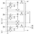
도 3은 도 1의 유기 발광 표시 장치에 포함된 리드아웃 회로의 일 예를 나타내는 회로도이다.3 is a circuit diagram showing an example of a lead-out circuit included in the organic light emitting diode display of FIG.
도 3을 참조하면, 리드아웃 회로(500)은 아날로그-디지털 변환부(510), 전류-전압 변환부(530), 및 스위치부를 포함할 수 있다.Referring to FIG. 3, the
아날로그-디지털 변환부(510)는 센싱 라인(RL(j/2))의 전압 및 전류-전압 변환부(530)의 출력 단자의 전압을 디지털 데이터로 변환할 수 있다. 일 실시예에서, 아날로그-디지털 변환부(510)는 샘플링-홀딩 회로(511) 및 아날로그-디지털 변환 회로(513)를 포함할 수 있다. 샘플링-홀딩 회로(511)는 센싱 라인(RL(j/2))의 전압 또는 전류-전압 변환부(530)의 출력 단자의 전압을 샘플링 및 홀딩하여 측정 전압으로 출력할 수 있다. 아날로그-디지털 변환 회로(513)는 측정 전압을 디지털 데이터로 변환할 수 있다.The analog-to-
전류-전압 변환부(530)는 센싱 라인(RL(j/2))으로부터 리드아웃 회로(500)로 흐르는 전류를 전압으로 변환할 수 있다. 예를 들어, 전류-전압 변환부(530)는 입력된 전류의 크기를 전압으로 변경하는 트랜스임피던스 증폭기(transimpedance amplifier)일 수 있다.The current-
일 실시예에서, 전류-전압 변환부(530)는 증폭기(531) 및 피드백 커패시터(CF)를 포함할 수 있다. 증폭기(531)는 스위치부를 통해 센싱 라인(RL(j/2))과 연결되는 제1 입력 단자, 제2 기준 전압(VRF2)이 인가되는 제2 입력 단자, 및 스위치부를 통해 아날로그-디지털 변환부(510)에 연결되는 출력 단자를 포함할 수 있다. 피드백 커패시터(CF)는 증폭기(531)의 출력 단자 및 증폭기(531)의 제1 입력 단자 사이에 연결될 수 있다.In one embodiment, the current-to-
스위치부는 센싱 라인(RL(j/2)), 전류-전압 변환부(530), 및 아날로그-디지털 변환부(510) 사이의 연결을 제어할 수 있다. 스위치부는 표시 구간에서 센싱 라인(RL(j/2))에 제1 기준 전원(VRF1)의 전압이 인가되도록 제어될 수 있다. 스위치부는 전압 센싱 구간에서 구동 트랜지스터의 문턱 전압을 측정하기 위해 센싱 라인(RL(j/2))과 아날로그-디지털 변환부(510)가 연결되도록 제어될 수 있다. 스위치부는 전류 센싱 구간에서 구동 트랜지스터의 이동도를 측정하기 위해 센싱 라인(RL(j/2))과 전류-전압 변환부(530)가 연결되고, 아날로그-디지털 변환부(510)과 전류-전압 변환부(530)가 연결되도록 제어될 수 있다.The switch section can control the connection between the sensing line RL (j / 2), the current-
일 실시예에서, 스위치부는 제1 내지 제6 스위칭 소자들(SW1 내지 SW6)을 포함할 수 있다. 제1 스위칭 소자(SW1)는 센싱 라인(RL(j/2)) 및 제1 기준 전원(VRF1) 사이에 위치할 수 있다. 제2 스위칭 소자(SW2)는 센싱 라인(RL(j/2)) 및 아날로그-디지털 변환부(510) 사이에 위치할 수 있다. 제3 스위칭 소자(SW3)는 센싱 라인(RL(j/2)) 및 전류-전압 변환부(530) 사이에 위치할 수 있다. 제4 스위칭 소자(SW4)는 전류-전압 변환부(530) 및 아날로그-디지털 변환부(510) 사이에 위치할 수 있다. 제5 스위칭 소자(SW5)는 아날로그-디지털 변환부(510) 및 리셋 전원(VRS) 사이에 위치할 수 있다. 제6 스위칭 소자(SW6)는 증폭기(531)의 제1 입력 단자 및 증폭기(531)의 제2 입력 단자 사이에 위치할 수 있다. 다만, 제1 내지 제6 스위칭 소자들(SW1 내지 SW6)의 동작에 대해서는 도 4 내지 도 9를 참조하여 자세히 설명하기로 한다.In one embodiment, the switch unit may include the first to sixth switching elements SW1 to SW6. The first switching element SW1 may be located between the sensing line RL (j / 2) and the first reference power supply VRF1. The second switching element SW2 may be located between the sensing line RL (j / 2) and the analog-to-
도 4 및 도 5는 표시 구간에서 유기 발광 표시 장치의 동작을 설명하기 위한 도면들이다.FIGS. 4 and 5 are views for explaining the operation of the OLED display in the display period.
도 4 및 도 5를 참조하면, 리드아웃 회로(500)는 표시 구간에서 센싱 라인(RL(j/2))에 제1 기준 전원(VRF1)의 전압을 인가하고, 화소들은 순차적으로 출력되는 스캔 신호에 응답하여 데이터 신호에 상응하는 빛을 발광할 수 있다.4 and 5, the lead-
표시 구간의 일 수평 기간(1H) 동안, 리드아웃 회로(500)의 제1 스위칭 소자(SW1)는 턴-온되고, 제2 내지 제6 스위칭 소자들(SW2 내지 SW6)은 턴-오프될 수 있다. 따라서, 리드아웃 회로(500)는 표시 구간에서 구동 트랜지스터의 특성 편차를 측정하지 않고 영상이 정상적으로 표시되도록 센싱 라인(RL(j/2))에 제1 기준 전원(VRF1)을 인가할 수 있다. 스캔 구동부는 스캔 라인들에 스캔 신호를 순차적으로 출력할 수 있다. 예를 들어, 제2 트랜지스터(T2-1/T2-2) 및 제3 트랜지스터(T3-1/T3-2)는 스캔 신호에 각각 응답하여 동시에 턴-온될 수 있다. 스토리지 커패시터(CST-1/CST-2)는 데이터 신호(VDATA(j-1)/VDATA(j))와 제1 기준 전압(VRF1)의 차이에 상응하는 충전 전압을 충전할 수 있다. 제2 트랜지스터(T2-1/T2-2) 및 제3 트랜지스터(T3-1/T3-2)가 턴-오프되더라도 스토리지 커패시터(CST-1/CST-2)는 충전 전압을 구동 트랜지스터인 제1 트랜지스터(T1-1/T1-2)의 구동 전압으로 공급할 수 있다. 유기 발광 다이오드(OLED-1/OLED-2)의 제2 전극에는 제2 전원(ELVSS)의 전압이 인가될 수 있다. 따라서, 유기 발광 다이오드(OLED-1/OLED-2)에는 구동 전압에 대응하는 구동 전류가 흐르고, 화소들은 데이터 신호에 상응하는 빛을 발광할 수 있다.During one horizontal period (1H) of the display period, the first switching device SW1 of the
도 6 및 도 7은 전압 센싱 구간에서 유기 발광 표시 장치의 동작을 설명하기 위한 도면들이다.6 and 7 are views for explaining the operation of the OLED display in a voltage sensing period.
도 6 및 도 7을 참조하면, 리드아웃 회로(500)는 전압 센싱 구간(PV)에서 센싱 라인(RL(j/2))과 아날로그-디지털 변환부를 연결하고 제1 화소의 구동 트랜지스터인 제1 트랜지스터(T1-1)의 문턱 전압을 측정할 수 있다.Referring to FIGS. 6 and 7, the lead-
센싱 라인(RL(j/2))을 공유하는 제1 및 제2 화소들은 전압 센싱 구간(PV)에서 연결된 스캔 라인(SL(i))으로부터 스캔 신호를 수신할 수 있다. 하나의 전압 센싱 구간(PV)에서 센싱 라인(RL(j/2))을 통해 하나의 구동 트랜지스터의 문턱 전압을 측정할 수 있으므로, 제1 화소는 전압 센싱 구간(PV)에서 데이터 신호로서 기 지정된 제1 데이터 전압(VDATA)을 수신하고 제2 화소는 데이터 신호로서 블랙 데이터에 상응하는 제2 데이터 전압(BLACK)을 수신할 수 있다. 또한, 전압 센싱 구간(PV)에서 제3 스위칭 소자(SW3), 제4 스위칭 소자(SW4), 제5 스위칭 소자(SW5), 및 제6 스위칭 소자(SW6)는 턴-오프될 수 있다.The first and second pixels sharing the sensing line RL (j / 2) may receive the scan signal from the scan line SL (i) connected in the voltage sensing period PV. Since the threshold voltage of one driving transistor can be measured through the sensing line RL (j / 2) in one voltage sensing period PV, the first pixel can be pre-specified as a data signal in the voltage sensing period PV The second pixel receives a first data voltage (VDATA) and the second pixel receives a second data voltage (BLACK) corresponding to black data as a data signal. In the voltage sensing period PV, the third, fourth, fifth, and sixth switching elements SW3, SW4, SW5, and SW6 may be turned off.
전압 센싱 구간(PV)의 제1 구간(PV1)에서 제1 스위칭 소자(SW1)는 턴-온되고, 제2 스위칭 소자(SW2)는 턴-오프될 수 있다. 따라서, 제1 구간(PV1)에서 센싱 라인(RL(j/2))에 제1 기준 전압(VRF1)이 인가되고, 센싱 라인(RL(j/2))은 초기화될 수 있다.The first switching device SW1 may be turned on and the second switching device SW2 may be turned off in the first section PV1 of the voltage sensing period PV. Therefore, the first reference voltage VRF1 may be applied to the sensing line RL (j / 2) in the first section PV1 and the sensing line RL (j / 2) may be initialized.
전압 센싱 구간(PV)의 제2 구간(PV2)에서 제1 스위칭 소자(SW1) 및 제2 스위칭 소자(SW2)는 턴-온될 수 있다. 따라서, 제2 구간(PV2)에서 아날로그-디지털 변환부의 샘플링-홀딩 회로(511)에 제1 기준 전원(VRF1)의 전압이 인가되고, 샘플링-홀딩 회로(511)는 초기화될 수 있다.In the second period PV2 of the voltage sensing period PV, the first switching device SW1 and the second switching device SW2 may be turned on. Therefore, in the second section PV2, the voltage of the first reference power supply VRF1 is applied to the sampling-and-holding
전압 센싱 구간(PV)의 제3 구간(PV3)에서 제1 스위칭 소자(SW1)는 턴-오프되고, 제2 스위칭 소자(SW2)는 턴-온될 수 있다. 제1 화소에서, 제1 트랜지스터(T1-1)로부터 흐르는 전류가 턴-온된 제3 트랜지스터(T3-1)와 센싱 라인(RL(j/2))을 경유하여 출력되고, 제1 트랜지스터(T1-1)로부터 흐르는 전류에 비례하여 센싱 라인(RL(j/2))의 전압이 상승할 수 있다. 스토리지 커패시터(CST-1)의 전압이 제1 트랜지스터(T1-1)의 문턱 전압(VTH)에 도달하면, 센싱 라인(RL(j/2))의 전압은 제1 데이터 전압(VDATA)과 제1 트랜지스터(T1-1)의 문턱 전압(VTH)과의 차이 전압(VDATA - VTH)에서 포화 상태가 될 수 있다. 이 때, 센싱 라인(RL(j/2))의 전압(VDATA - VTH)을 샘플링함으로써, 구동 트랜지스터인 제1 트랜지스터(T1-1)의 문턱 전압(VTH)를 측정할 수 있다.The first switching device SW1 may be turned off and the second switching device SW2 may be turned on in the third period PV3 of the voltage sensing period PV. In the first pixel, a current flowing from the first transistor T1-1 is output via the third transistor T3-1 and the sensing line RL (j / 2) which are turned on, and the first transistor T1 -1), the voltage of the sensing line RL (j / 2) may rise. When the voltage of the storage capacitor CST-1 reaches the threshold voltage VTH of the first transistor T1-1, the voltage of the sensing line RL (j / 2) becomes equal to the first data voltage VDATA, Can be saturated at a difference voltage (VDATA - VTH) from the threshold voltage (VTH) of one transistor (T1-1). At this time, the threshold voltage VTH of the first transistor T1-1 as the driving transistor can be measured by sampling the voltage VDATA-VTH of the sensing line RL (j / 2).
도 8 및 도 9는 전류 센싱 구간에서 유기 발광 표시 장치의 동작을 설명하기 위한 도면들이다.8 and 9 are views for explaining the operation of the OLED display in a current sensing period.
도 8 및 도 9를 참조하면, 리드아웃 회로(500)는 전류 센싱 구간(PI)에서 센싱 라인(RL(j/2))과 전류-전압 변환부를 연결하고 전류-전압 변환부와 아날로그-디지털 변환부를 연결하며, 구동 트랜지스터인 제1 트랜지스터(T1-1)의 이동도를 측정할 수 있다.8 and 9, the lead-
센싱 라인(RL(j/2))을 공유하는 제1 및 제2 화소들은 전류 센싱 구간(PI)에서 연결된 스캔 라인(SL(i))으로부터 스캔 신호를 수신할 수 있다. 하나의 전류 센싱 구간(PI)에서 센싱 라인(RL(j/2))을 통해 하나의 구동 트랜지스터의 이동도를 측정할 수 있으므로, 제1 화소는 전류 센싱 구간(PI)에서 데이터 신호로서 기 지정된 제1 데이터 전압(VDATA)을 수신하고 제2 화소는 데이터 신호로서 블랙 데이터에 상응하는 제2 데이터 전압(BLACK)을 수신할 수 있다. 또한, 전류 센싱 구간(PI)에서 전류-전압 변환부를 동작시키기 위해 제1 스위칭 소자(SW1) 및 제2 스위칭 소자(SW2)는 턴-오프되고, 제3 스위칭 소자(SW3) 및 제4 스위칭 소자(SW4)는 턴-온될 수 있다.The first and second pixels sharing the sensing line RL (j / 2) may receive the scan signal from the scan line SL (i) connected in the current sensing period PI. Since the mobility of one driving transistor can be measured through the sensing line RL (j / 2) in one current sensing period PI, the first pixel can be pre-specified as a data signal in the current sensing period PI The second pixel receives a first data voltage (VDATA) and the second pixel receives a second data voltage (BLACK) corresponding to black data as a data signal. In order to operate the current-voltage converter in the current sensing period PI, the first switching device SW1 and the second switching device SW2 are turned off and the third switching device SW3 and the fourth switching device SW2 are turned off. The switch SW4 may be turned on.
전류 센싱 구간(PI)의 제1 구간(PI1)에서 제5 스위칭 소자(SW5) 및 제6 스위칭 소자(SW6)는 턴-온될 수 있다. 따라서, 제1 구간(PV1)에서 센싱 라인(RL(j/2))에 제2 기준 전원(VRF2)의 전압이 인가되고, 센싱 라인(RL(j/2))은 초기화될 수 있다. 또한, 제1 구간(PV1)에서 아날로그-디지털 변환부의 샘플링-홀딩 회로(511)에 리셋 전원(VRS)의 전압이 인가되고, 아날로그-디지털 변환부의 샘플링-홀딩 회로(511)는 초기화될 수 있다.The fifth switching element SW5 and the sixth switching element SW6 may be turned on in the first period PI1 of the current sensing period PI. Therefore, the voltage of the second reference power supply VRF2 is applied to the sensing line RL (j / 2) in the first section PV1 and the sensing line RL (j / 2) can be initialized. Also, in the first section PV1, the voltage of the reset power source VRS is applied to the sampling-and-holding
전류 센싱 구간(PI)의 제2 구간(PI2)에서 제5 스위칭 소자(SW5) 및 제6 스위칭 소자(SW6)는 턴-오프될 수 있다. 따라서, 아날로그-디지털 변환부의 샘플링-홀딩 회로(511)에는 리셋 전원(VRS)의 전압이 더 이상 인가되지 않는다. 제1 화소에서, 구동 트랜지스터인 제1 트랜지스터(T1-1)의 게이트 전극에는 제1 데이터 전압이 인가될 수 있다. 전류-전압 변환부에 포함된 증폭기의 가상 단락(virtual short)에 의해 제1 트랜지스터(T1-1)의 제2 전극에는 제2 기준 전압(VRF2)이 인가될 수 있다. 그 결과, 제1 트랜지스터(T1-1)의 구동 전압은 제1 데이터 전압(VDATA)과 제2 기준 전압(VRF2)의 차이 전압(VDATA-VRF2)이 될 수 있다. 트랜스임피던스 증폭기(transimpedance amplifier)인 전류-전압 변환부의 동작에 의해 샘플링-홀딩 회로(511)에 인가되는 전압(VADC)은 리셋 전원(VRS)의 전압으로부터 점차 감소할 수 있다. 여기서, 제1 트랜지스터의 이동도는 [수학식 1]을 이용하여 도출할 수 있다.The fifth switching element SW5 and the sixth switching element SW6 may be turned off in the second period PI2 of the current sensing period PI. Therefore, the voltage of the reset power supply VRS is no longer applied to the sampling-and-holding
[수학식 1][Equation 1]

여기서, VADC는 샘플링-홀딩 회로에 인가되는 전압, VRS는 리셋 전원의 전압, C는 피드백 커패시터의 커패시턴스, t는 전압이 하강된 시간, I는 측정 전류를 나타낸다. 따라서, 측정 전류값은 피드백 커패시터의 커패시턴스, 전압 하강 시간, 전압 하강 시간에 따른 하강된 전압을 이용하여 계산될 수 있다.Here, VADC represents the voltage applied to the sampling-holding circuit, VRS represents the voltage of the reset power source, C represents the capacitance of the feedback capacitor, t represents the time when the voltage has fallen, and I represents the measured current. Therefore, the measured current value can be calculated by using the capacitance of the feedback capacitor, the voltage drop time, and the dropped voltage according to the voltage drop time.
도 10은 본 발명의 다른 실시예에 따른 유기 발광 표시 장치를 나타내는 블록도이다.10 is a block diagram illustrating an organic light emitting display according to another embodiment of the present invention.
도 10을 참조하면, 유기 발광 표시 장치(1000B)는 표시 패널(100B), 스캔 구동부(300), 데이터 구동부(400), 리드아웃 회로(500), 전원 공급부(700), 및 제어부(900)를 포함할 수 있다. 다만, 본 실시예에 따른 유기 발광 표시 장치(1000B)는 동일한 스캔 라인에 연결된 3개의 화소들이 동일한 센싱 라인을 공유하는 것을 제외하면, 도 1의 유기 발광 표시 장치와 실질적으로 동일하므로, 동일 또는 유사한 구성 요소에 대해서는 동일한 참조 번호를 사용하고, 중복되는 설명은 생략하기로 한다.10, the
표시 패널(100B)은 복수의 화소(PX)들을 포함할 수 있다. 예를 들어, 표시 패널(100B)은 스캔 라인들(SL1 내지 SLn) 및 데이터 라인들(DL1 내지 DLm)의 교차부마다 위치되는 n*m 개의 화소(PX)들을 포함할 수 있다. 스캔 라인들(SL1 내지 SLn) 중 하나와 연결된 3개의 화소들은 표시 패널(100B)의 개구율을 높이기 위해 하나의 센싱 라인에 연결될 수 있다. 즉, 동일한 수평 라인 상에 위치하고 서로 인접한 제1 내지 제3 화소들은 하나의 센싱 라인을 공유할 수 있다.The
스캔 구동부(300)는 제1 제어 신호(CTL1)에 기초하여 스캔 라인들(SL1 내지 SLn)을 통해 화소(PX)들에 스캔 신호를 제공할 수 있다.The
데이터 구동부(400)는 제2 제어 신호(CTL2)에 기초하여 데이터 라인들(DL1 내지 DLm)을 통해 화소(PX)들에 데이터 신호를 제공할 수 있다.The
리드아웃 회로(500)는 복수의 센싱 라인들(RL1 내지 RL(m/2))을 통해 화소(PX)들에 연결될 수 있다. 리드아웃 회로(500)는 제3 제어 신호(CTL3)에 기초하여 구동 트랜지스터의 특성 편차(즉, 문턱 전압 및 이동도)를 측정하고, 측정된 특성 편차에 대한 피드백 정보(FB)를 제어부(900)로 제공할 수 있다.The lead-
전원 공급부(700)는 제4 제어 신호(CTL4)에 기초하여 전원을 표시 패널(100B)에 제공할 수 있다. 전원 공급부(700)는 제1 전원(ELVDD) 및 제2 전원(ELVSS)을 생성하여 표시 패널(100B)에 제공할 수 있다.The
제어부(900)는 입력 제어 신호(CTL)를 수신하고, 스캔 구동부(300), 데이터 구동부(400), 리드아웃 회로(500), 및 전원 공급부(700)를 제어하기 위해 입력 제어 신호(CTL)에 기초하여 제1 내지 제4 제어 신호들(CTL1 내지 CTL4)를 생성할 수 있다. 또한, 제어부(900)는 구동 트랜지스터의 특성 편차에 대한 피드백 정보(FB)를 리드아웃 회로(500)로부터 수신할 수 있다. 제어부(900)는 구동 트랜지스터의 특성 편차를 보상하기 위해 피드백 정보(FB)에 기초하여 입력 영상 데이터(IDATA)를 출력 영상 데이터(ODATA)로 변환할 수 있다.The
도 11은 도 10의 유기 발광 표시 장치에 포함된 화소의 일 예를 나타내는 회로도이다.11 is a circuit diagram showing an example of a pixel included in the organic light emitting diode display of FIG.
도 11을 참조하면, 화소들(PX1/PX2/PX3)은 동일한 스캔 신호에 의해 턴-온되는 데이터 라인(DL(j-2)/DL(j-1)/DLj)에 연결된 트랜지스터(T2-1/T2-2/T2-3)와 센싱 라인(RL(j/3))에 연결된 트랜지스터(T3-1/T3-2/T3-3)를 포함할 수 있다.11, the pixels PX1 / PX2 / PX3 are connected to the data lines DL (j-2) / DL (j-1) / DLj which are turned on by the same scan signal, (T3-1 / T3-2 / T3-3) connected to the sensing line RL (j / 3).
일 실시예에서, 화소들(PX1/PX2/PX3) 각각은 제1 트랜지스터(T1-1/T1-2/T1-3), 제2 트랜지스터(T2-1/T2-2/T2-3), 제3 트랜지스터(T3-1/T3-1/T3-1), 스토리지 커패시터(CST-1/CST-2/CST-3), 및 유기 발광 다이오드(OLED-1/OLED-2/OLED-3)를 포함할 수 있다. 다만, 화소의 구조에 대해서는 상술한 바 있으므로, 그에 대한 중복되는 설명은 생략하기로 한다.In one embodiment, each of the pixels PX1 / PX2 / PX3 includes a first transistor T1-1 / T1-2 / T1-3, a second transistor T2-1 / T2-2 / T2-3, (OLED-1 / OLED-2 / OLED-3), the third transistor (T3-1 / T3-1 / T3-1), the storage capacitor . ≪ / RTI > However, since the structure of the pixel has been described above, a duplicate description thereof will be omitted.
동일한 스캔 라인(SLi) 상에 위치하는 제1 내지 제3 화소들(PX1 내지 PX3)은 하나의 센싱 라인(RL(j/3))을 공유할 수 있다. 예를 들어, 표시 패널(100B)에는 화소들이 스트라이프(stripe) 구조로 배치되고, 제1 내지 제3 화소들(PX1 내지 PX3)은 각각 적색 유기 발광 다이오드, 녹색 유기 발광 다이오드, 및 청색 유기 발광 다이오드를 포함할 수 있다. 복수의 화소들이 하나의 센싱 라인(RL(j/3))을 공유하는 경우 센싱 라인(RL(j/3))의 개수를 줄일 수 있으므로 표시 패널(100B)의 개구율을 높일 수 있다.The first through third pixels PX1 through PX3 located on the same scan line SLi may share one sensing line RL (j / 3). For example, in the
일 실시예에서, 제1 내지 제3 화소들(PX1 내지 PX3) 중 하나는 전압 센싱 구간 및 전류 센싱 구간에서 데이터 신호로서 기 지정된 제1 데이터 전압을 수신할 수 있다. 또한, 제1 내지 제3 화소들(PX1 내지 PX3) 중 하나를 제외한 나머지 화소들은 전압 센싱 구간 및 전류 센싱 구간에서 데이터 신호로서 블랙 데이터에 상응하는 제2 데이터 전압을 수신할 수 있다. 하나의 전압 센싱 구간 또는 전류 센싱 구간에서 센싱 라인(RL(j/3))을 통해 하나의 구동 트랜지스터의 문턱 전압 또는 이동도를 측정할 수 있으므로, 제1 내지 제3 화소들(PX1 내지 PX3) 중 하나를 제외한 나머지 화소들은 전압 센싱 구간 및 전류 센싱 구간에서 데이터 신호로서 블랙 데이터에 상응하는 제2 데이터 전압을 수신할 수 있다.In one embodiment, one of the first to third pixels PX1 to PX3 may receive the first data voltage, which is previously designated as a data signal in the voltage sensing period and the current sensing period. The remaining pixels except for one of the first through third pixels PX1 through PX3 may receive a second data voltage corresponding to black data as a data signal in a voltage sensing period and a current sensing period. The threshold voltage or the mobility of one driving transistor can be measured through the sensing line RL (j / 3) in one voltage sensing period or current sensing period, so that the first to third pixels PX1 to PX3, May receive the second data voltage corresponding to the black data as the data signal in the voltage sensing period and the current sensing period.
따라서, 동일한 스캔 라인(SLi) 상에 위치하는 제1 내지 제3 화소들(PX1 내지 PX3)은 하나의 센싱 라인(RL(j/3))을 공유함으로서 표시 패널(100B)의 개구율을 향상시킬 수 있다.Therefore, the first through third pixels PX1 through PX3 located on the same scan line SLi share one sensing line RL (j / 3), thereby improving the aperture ratio of the
이상, 본 발명의 실시예들에 따른 리드아웃 회로 및 이를 포함하는 유기 발광 표시 장치에 대하여 도면을 참조하여 설명하였지만, 상기 설명은 예시적인 것으로서 본 발명의 기술적 사상을 벗어나지 않는 범위에서 해당 기술 분야에서 통상의 지식을 가진 자에 의하여 수정 및 변경될 수 있을 것이다. 예를 들어, 상기에서는 리드아웃 회로와 데이터 구동부가 분리된 것으로 설명하였으나, 리드아웃 회로와 데이터 구동부는 동일한 집적 회로에 구현될 수 있다.While the present invention has been particularly shown and described with reference to exemplary embodiments thereof, it is to be understood that the invention is not limited to the disclosed exemplary embodiments, Modifications and alterations may occur to those skilled in the art. For example, in the above description, the readout circuit and the data driver are separated, but the readout circuit and the data driver may be implemented in the same integrated circuit.
본 발명은 표시 장치를 구비한 전자 기기에 다양하게 적용될 수 있다. 예를 들어, 본 발명은 컴퓨터, 노트북, 휴대폰, 스마트폰, 스마트패드, 피엠피(PMP), 피디에이(PDA), MP3 플레이어, 디지털 카메라, 비디오 캠코더 등에 적용될 수 있다.The present invention can be variously applied to an electronic apparatus having a display device. For example, the present invention can be applied to a computer, a notebook, a mobile phone, a smart phone, a smart pad, a PMP, a PDA, an MP3 player, a digital camera, a video camcorder,
상기에서는 본 발명의 실시예들을 참조하여 설명하였지만, 해당 기술분야에서 통상의 지식을 가진 자는 하기의 특허청구범위에 기재된 본 발명의 사상 및 영역으로부터 벗어나지 않는 범위 내에서 본 발명을 다양하게 수정 및 변경시킬 수 있음을 이해할 것이다.While the present invention has been particularly shown and described with reference to exemplary embodiments thereof, it will be understood by those skilled in the art that various changes and modifications may be made therein without departing from the spirit and scope of the invention as defined in the appended claims. You will understand.
100A, 100B: 표시 패널300: 스캔 구동부
400: 데이터 구동부500: 리드아웃 회로
510: 아날로그-디지털 변환부530: 전류-전압 변환부
700: 전원 공급부900: 제어부
1000A, 1000B: 유기 발광 표시 장치100A, 100B: display panel 300: scan driver
400: Data driver 500: Lead-out circuit
510: analog-to-digital conversion unit 530: current-voltage conversion unit
700: Power supply unit 900: Control unit
1000A, 1000B: organic light emitting display
Claims (20)
Translated fromKorean복수의 스캔 라인들을 통해 상기 화소들에 스캔 신호를 제공하는 스캔 구동부;
복수의 데이터 라인들을 통해 상기 화소들에 데이터 신호를 제공하는 데이터 구동부; 및
복수의 센싱 라인들을 통해 상기 화소들에 연결되는 리드아웃 회로를 포함하고,
상기 리드아웃 회로는
상기 센싱 라인들 중 하나로부터 상기 리드아웃 회로로 흐르는 전류를 전압으로 변환하는 전류-전압 변환부;
상기 센싱 라인들 중 상기 하나의 전압 및 상기 전류-전압 변환부의 출력 단자의 전압을 디지털 데이터로 변환하는 아날로그-디지털 변환부; 및
상기 센싱 라인들 중 상기 하나, 상기 전류-전압 변환부, 및 상기 아날로그-디지털 변환부 사이의 연결을 제어하는 스위치부를 포함하는 것을 특징으로 하는 유기 발광 표시 장치.A display panel including a plurality of pixels;
A scan driver for supplying a scan signal to the pixels through a plurality of scan lines;
A data driver for supplying a data signal to the pixels through a plurality of data lines; And
And a readout circuit connected to the pixels through a plurality of sensing lines,
The lead-out circuit
A current-to-voltage converter converting a current flowing from one of the sensing lines to the readout circuit into a voltage;
An analog-to-digital converter converting the one of the sensing lines and the voltage of the output terminal of the current-voltage converter into digital data; And
And a switch unit for controlling connection between the one of the sensing lines, the current-voltage conversion unit, and the analog-digital conversion unit.
상기 센싱 라인들 중 상기 하나 및 제1 기준 전원 사이에 위치하는 제1 스위칭 소자;
상기 센싱 라인들 중 상기 하나 및 상기 아날로그-디지털 변환부 사이에 위치하는 제2 스위칭 소자;
상기 센싱 라인들 중 상기 하나 및 상기 전류-전압 변환부 사이에 위치하는 제3 스위칭 소자;
상기 상기 전류-전압 변환부 및 상기 아날로그-디지털 변환부 사이에 위치하는 제4 스위칭 소자; 및
상기 아날로그-디지털 변환부 및 리셋 전원 사이에 위치하는 제5 스위칭 소자를 포함하는 것을 특징으로 하는 유기 발광 표시 장치.The apparatus as claimed in claim 1,
A first switching device positioned between the one of the sensing lines and the first reference power supply;
A second switching element positioned between the one of the sensing lines and the analog-to-digital conversion section;
A third switching device positioned between the one of the sensing lines and the current-voltage conversion unit;
A fourth switching device positioned between the current-voltage conversion unit and the analog-digital conversion unit; And
And a fifth switching element located between the analog-digital converter and the reset power source.
상기 제2 스위칭 소자 및 제3 스위칭 소자는 상기 표시 구간에서 턴-오프되는 것을 특징으로 하는 유기 발광 표시 장치The method of claim 2, wherein the first switching element is turned on in a display period,
And the second switching element and the third switching element are turned off in the display period.
상기 제3 스위칭 소자, 상기 제4 스위칭 소자, 및 상기 제5 스위칭 소자는 상기 전압 센싱 구간에서 턴-오프되는 것을 특징으로 하는 유기 발광 표시 장치.3. The method of claim 2, wherein the second switching element is turned on at least a portion of a voltage sensing period,
Wherein the third switching element, the fourth switching element, and the fifth switching element are turned off in the voltage sensing period.
상기 제3 스위칭 소자 및 상기 제4 스위칭 소자는 상기 전류 센싱 구간에서 턴-온되는 것을 특징으로 하는 유기 발광 표시 장치.The method of claim 2, wherein the first switching element and the second switching element are turned off in a current sensing period,
And the third switching device and the fourth switching device are turned on in the current sensing period.
상기 센싱 라인들 중 상기 하나의 전압 또는 상기 전류-전압 변환부의 출력 단자의 전압을 샘플링 및 홀딩하여 측정 전압으로 출력하는 샘플링-홀딩 회로; 및
상기 측정 전압을 디지털 데이터로 변환하는 아날로그-디지털 변환 회로를 포함하는 것을 특징으로 하는 유기 발광 표시 장치.The apparatus as claimed in claim 1, wherein the analog-to-digital converter
A sampling-holding circuit for sampling and holding the voltage of the one of the sensing lines or the voltage of the output terminal of the current-voltage conversion unit and outputting the voltage as a measurement voltage; And
And an analog-to-digital conversion circuit for converting the measured voltage into digital data.
상기 스위치부를 통해 상기 센싱 라인들 중 상기 하나와 연결되는 제1 입력 단자, 제2 기준 전압이 인가되는 제2 입력 단자, 및 상기 스위치부를 통해 상기 아날로그-디지털 변환부에 연결되는 출력 단자를 포함하는 증폭기; 및
상기 증폭기의 상기 출력 단자 및 상기 증폭기의 상기 제1 입력 단자 사이에 연결된 피드백 커패시터를 포함하는 것을 특징으로 하는 유기 발광 표시 장치.2. The apparatus of claim 1, wherein the current-voltage converter
A first input terminal connected to the one of the sensing lines through the switch unit, a second input terminal to which a second reference voltage is applied, and an output terminal connected to the analog-digital converter through the switch unit amplifier; And
And a feedback capacitor connected between the output terminal of the amplifier and the first input terminal of the amplifier.
상기 증폭기의 상기 제1 입력 단자 및 상기 증폭기의 상기 제2 입력 단자 사이에 위치하는 제6 스위칭 소자를 포함하는 것을 특징으로 하는 유기 발광 표시 장치.10. The apparatus as claimed in claim 9, wherein the switch unit
And a sixth switching element positioned between the first input terminal of the amplifier and the second input terminal of the amplifier.
제1 노드에 연결된 게이트 전극, 제1 전원에 연결된 제1 전극, 및 제2 노드에 연결된 제2 전극을 포함하는 제1 트랜지스터;
상기 스캔 라인들 중 하나에 연결된 게이트 전극, 상기 데이터 라인들 중 하나에 연결된 제1 전극, 및 상기 제1 노드에 연결된 제2 전극을 포함하는 제2 트랜지스터;
상기 스캔 라인들 중 상기 하나에 연결된 게이트 전극, 상기 제2 노드에 연결된 제1 전극 및 상기 센싱 라인들 중 상기 하나에 연결된 제2 전극을 포함하는 제3 트랜지스터;
상기 제1 노드 및 상기 제2 노드 사이에 연결된 스토리지 커패시터; 및
상기 제2 노드에 연결된 제1 전극 및 상기 제1 전원 또는 제2 전원에 선택적으로 연결되는 제2 전극을 포함하는 유기 발광 다이오드를 포함하는 것을 특징으로 하는 유기 발광 표시 장치.2. The method of claim 1, wherein each of the pixels
A first transistor including a gate electrode coupled to a first node, a first electrode coupled to a first power supply, and a second electrode coupled to a second node;
A second transistor including a gate electrode coupled to one of the scan lines, a first electrode coupled to one of the data lines, and a second electrode coupled to the first node;
A third transistor including a gate electrode connected to the one of the scan lines, a first electrode connected to the second node, and a second electrode connected to the one of the sensing lines;
A storage capacitor coupled between the first node and the second node; And
And an organic light emitting diode including a first electrode connected to the second node and a second electrode selectively connected to the first power source or the second power source.
상기 제1 내지 제3 화소들은 각각 적색 유기 발광 다이오드, 녹색 유기 발광 다이오드, 및 청색 유기 발광 다이오드를 포함하는 것을 특징으로 하는 유기 발광 표시 장치.15. The display device of claim 14, wherein the first to third pixels connected to one of the scan lines among the pixels are connected to one of the sensing lines,
Wherein the first to third pixels include a red organic light emitting diode, a green organic light emitting diode, and a blue organic light emitting diode, respectively.
상기 제1 내지 제3 화소들 중 상기 하나를 제외한 나머지 화소들은 상기 전압 센싱 구간 및 상기 전류 센싱 구간에서 상기 데이터 신호로서 블랙 데이터에 상응하는 제2 데이터 전압을 수신하는 것을 특징으로 하는 유기 발광 표시 장치.The method of claim 15, wherein one of the first to third pixels receives the first data voltage designated as the data signal in the voltage sensing period and the current sensing period,
Wherein the pixels other than the one of the first through third pixels receive the second data voltage corresponding to the black data as the data signal in the voltage sensing period and the current sensing period. .
상기 센싱 라인의 전압 및 상기 전류-전압 변환부의 출력 단자의 전압을 디지털 데이터로 변환하는 아날로그-디지털 변환부; 및
상기 센싱 라인, 상기 전류-전압 변환부, 및 상기 아날로그-디지털 변환부 사이의 연결을 제어하는 스위치부를 포함하는 리드아웃 회로.A current-to-voltage converter for converting a current flowing from the sensing line into a voltage;
An analog-digital converter for converting the voltage of the sensing line and the voltage of the output terminal of the current-voltage converter into digital data; And
And a switch section for controlling a connection between the sensing line, the current-voltage conversion section, and the analog-digital conversion section.
상기 센싱 라인 및 제1 기준 전원 사이에 위치하는 제1 스위칭 소자;
상기 센싱 라인 및 상기 아날로그-디지털 변환부 사이에 위치하는 제2 스위칭 소자;
상기 센싱 라인 및 상기 전류-전압 변환부 사이에 위치하는 제3 스위칭 소자;
상기 상기 전류-전압 변환부 및 상기 아날로그-디지털 변환부 사이에 위치하는 제4 스위칭 소자; 및
상기 아날로그-디지털 변환부 및 리셋 전원 사이에 위치하는 제5 스위칭 소자를 포함하는 것을 특징으로 하는 리드아웃 회로.18. The apparatus of claim 17, wherein the switch portion
A first switching device positioned between the sensing line and a first reference power supply;
A second switching element positioned between the sensing line and the analog-digital converter;
A third switching device positioned between the sensing line and the current-voltage conversion unit;
A fourth switching device positioned between the current-voltage conversion unit and the analog-digital conversion unit; And
And a fifth switching element positioned between the analog-to-digital converter and the reset power supply.
상기 스위치부를 통해 상기 센싱 라인과 연결되는 제1 입력 단자, 제2 기준 전압이 인가되는 제2 입력 단자, 및 상기 스위치부를 통해 상기 아날로그-디지털 변환부에 연결되는 출력 단자를 포함하는 증폭기; 및
상기 증폭기의 상기 출력 단자 및 상기 증폭기의 상기 제1 입력 단자 사이에 연결된 피드백 커패시터를 포함하는 것을 특징으로 하는 리드아웃 회로.18. The method of claim 17, wherein the current-voltage converter
An amplifier including a first input terminal connected to the sensing line through the switch unit, a second input terminal to which a second reference voltage is applied, and an output terminal connected to the analog-digital converter through the switch unit; And
And a feedback capacitor coupled between the output terminal of the amplifier and the first input terminal of the amplifier.
상기 증폭기의 상기 제1 입력 단자 및 상기 증폭기의 상기 제2 입력 단자 사이에 위치하는 제6 스위칭 소자를 포함하는 것을 특징으로 하는 리드아웃 회로.
20. The apparatus of claim 19, wherein the switch portion
And a sixth switching element located between the first input terminal of the amplifier and the second input terminal of the amplifier.
Priority Applications (2)
| Application Number | Priority Date | Filing Date | Title |
|---|---|---|---|
| KR1020150110599AKR102377779B1 (en) | 2015-08-05 | 2015-08-05 | Readout circuit and organic light emitting display device having the same |
| US15/059,848US9928776B2 (en) | 2015-08-05 | 2016-03-03 | Readout circuit and organic light emitting display device having the same |
Applications Claiming Priority (1)
| Application Number | Priority Date | Filing Date | Title |
|---|---|---|---|
| KR1020150110599AKR102377779B1 (en) | 2015-08-05 | 2015-08-05 | Readout circuit and organic light emitting display device having the same |
Publications (2)
| Publication Number | Publication Date |
|---|---|
| KR20170018135Atrue KR20170018135A (en) | 2017-02-16 |
| KR102377779B1 KR102377779B1 (en) | 2022-03-24 |
Family
ID=58052808
Family Applications (1)
| Application Number | Title | Priority Date | Filing Date |
|---|---|---|---|
| KR1020150110599AActiveKR102377779B1 (en) | 2015-08-05 | 2015-08-05 | Readout circuit and organic light emitting display device having the same |
Country Status (2)
| Country | Link |
|---|---|
| US (1) | US9928776B2 (en) |
| KR (1) | KR102377779B1 (en) |
Cited By (1)
| Publication number | Priority date | Publication date | Assignee | Title |
|---|---|---|---|---|
| WO2021096070A1 (en)* | 2019-11-13 | 2021-05-20 | 삼성디스플레이 주식회사 | Display device |
Families Citing this family (15)
| Publication number | Priority date | Publication date | Assignee | Title |
|---|---|---|---|---|
| CN106940978B (en)* | 2017-05-15 | 2019-10-25 | 上海天马有机发光显示技术有限公司 | Organic light emitting display panel and its driving method, organic light-emitting display device |
| CN106940984B (en)* | 2017-05-17 | 2019-12-13 | 上海天马有机发光显示技术有限公司 | organic light emitting display panel, driving method thereof and organic light emitting display device |
| CN107610643B (en)* | 2017-09-29 | 2020-11-10 | 京东方科技集团股份有限公司 | Compensation circuit and control method thereof, display panel and display device |
| CN107610647B (en)* | 2017-11-07 | 2020-04-10 | 京东方科技集团股份有限公司 | Driving module and method of pixel circuit and display device |
| KR102513528B1 (en) | 2018-07-16 | 2023-03-24 | 삼성디스플레이 주식회사 | Organic light emitting display device and a method of driving the same |
| KR20200019529A (en)* | 2018-08-14 | 2020-02-24 | 삼성전자주식회사 | Display driving circuit and operating method thereof |
| KR20200025880A (en)* | 2018-08-31 | 2020-03-10 | 삼성전자주식회사 | Display device and control method thereof |
| KR102575560B1 (en)* | 2018-11-08 | 2023-09-08 | 삼성디스플레이 주식회사 | Display device and method for driving the same |
| CN109493794B (en) | 2019-01-24 | 2020-05-29 | 鄂尔多斯市源盛光电有限责任公司 | Pixel circuit, pixel driving method and display device |
| KR102566281B1 (en)* | 2019-02-18 | 2023-08-16 | 삼성디스플레이 주식회사 | Display device and driving method thereof |
| US11062648B2 (en)* | 2019-05-13 | 2021-07-13 | Novatek Microelectronics Corp. | Display device and method of sensing the same |
| KR102693254B1 (en)* | 2019-08-20 | 2024-08-12 | 삼성디스플레이 주식회사 | Display device and driving method thereof |
| KR102819369B1 (en)* | 2019-12-26 | 2025-06-11 | 엘지디스플레이 주식회사 | DRD type display panel and Organic light emitting diode display device using the display panel |
| KR20240106225A (en)* | 2022-12-29 | 2024-07-08 | 엘지디스플레이 주식회사 | Display Device and Driving Method of the same |
| TWI876750B (en)* | 2023-01-30 | 2025-03-11 | 南韓商Lg顯示器股份有限公司 | Display panel, pixel circuit arranged therein and display device including the same |
Citations (4)
| Publication number | Priority date | Publication date | Assignee | Title |
|---|---|---|---|---|
| KR20110100219A (en)* | 2008-12-18 | 2011-09-09 | 글로벌 오엘이디 테크놀러지 엘엘씨 | Digital-Drive Electroluminescent Displays with Aging Compensation |
| KR20130024744A (en)* | 2011-08-30 | 2013-03-08 | 엘지디스플레이 주식회사 | Organic light emitting diode display device for sensing pixel current and method for sensing pixel current thereof |
| US20140022289A1 (en)* | 2012-07-19 | 2014-01-23 | Lg Display Co., Ltd. | Organic Light Emitting Diode Display Device for Sensing Pixel Current and Pixel Current Sensing Method Thereof |
| US20140176625A1 (en)* | 2012-12-21 | 2014-06-26 | Lg Display Co., Ltd. | ORGANIC LIGHT EMITTING DIODE DISPLAY DEVICE AND METHOD of DRIVING THE SAME |
Family Cites Families (1)
| Publication number | Priority date | Publication date | Assignee | Title |
|---|---|---|---|---|
| US9236011B2 (en) | 2011-08-30 | 2016-01-12 | Lg Display Co., Ltd. | Organic light emitting diode display device for pixel current sensing in the sensing mode and pixel current sensing method thereof |
- 2015
- 2015-08-05KRKR1020150110599Apatent/KR102377779B1/enactiveActive
- 2016
- 2016-03-03USUS15/059,848patent/US9928776B2/enactiveActive
Patent Citations (5)
| Publication number | Priority date | Publication date | Assignee | Title |
|---|---|---|---|---|
| KR20110100219A (en)* | 2008-12-18 | 2011-09-09 | 글로벌 오엘이디 테크놀러지 엘엘씨 | Digital-Drive Electroluminescent Displays with Aging Compensation |
| KR101267900B1 (en)* | 2008-12-18 | 2013-05-28 | 글로벌 오엘이디 테크놀러지 엘엘씨 | Digital-Drive Electroluminescent Display with Aging Compensation |
| KR20130024744A (en)* | 2011-08-30 | 2013-03-08 | 엘지디스플레이 주식회사 | Organic light emitting diode display device for sensing pixel current and method for sensing pixel current thereof |
| US20140022289A1 (en)* | 2012-07-19 | 2014-01-23 | Lg Display Co., Ltd. | Organic Light Emitting Diode Display Device for Sensing Pixel Current and Pixel Current Sensing Method Thereof |
| US20140176625A1 (en)* | 2012-12-21 | 2014-06-26 | Lg Display Co., Ltd. | ORGANIC LIGHT EMITTING DIODE DISPLAY DEVICE AND METHOD of DRIVING THE SAME |
Cited By (2)
| Publication number | Priority date | Publication date | Assignee | Title |
|---|---|---|---|---|
| WO2021096070A1 (en)* | 2019-11-13 | 2021-05-20 | 삼성디스플레이 주식회사 | Display device |
| US11848335B2 (en) | 2019-11-13 | 2023-12-19 | Samsung Display Co., Ltd. | Display device |
Also Published As
| Publication number | Publication date |
|---|---|
| KR102377779B1 (en) | 2022-03-24 |
| US9928776B2 (en) | 2018-03-27 |
| US20170039952A1 (en) | 2017-02-09 |
Similar Documents
| Publication | Publication Date | Title |
|---|---|---|
| KR102377779B1 (en) | Readout circuit and organic light emitting display device having the same | |
| US20230038819A1 (en) | Systems and methods of pixel calibration based on improved reference values | |
| US11056065B2 (en) | Light-emitting display for compensating degradation of organic light-emitting diode and method of driving the same | |
| US11049459B2 (en) | Light-emitting display and method of driving the same | |
| CN107799060B (en) | Organic light emitting display and degradation sensing method thereof | |
| US11030951B2 (en) | Light-emitting display and method of driving the same | |
| TWI576811B (en) | Sensing circuit and organic light emitting diode ?display device having the same | |
| US9818341B2 (en) | Organic light-emitting display device and method of driving the same | |
| CN101551970B (en) | Light-emitting device, display device and drive control method for light-emitting device | |
| US20200058252A1 (en) | Display driving circuit and operating method thereof | |
| KR102686300B1 (en) | Method for compensating degradation of display device | |
| KR100966502B1 (en) | Driving circuit and driving method of light emitting display device | |
| KR102595281B1 (en) | Data Driver and Display Device using the same | |
| CN110853582B (en) | Pixel, control method thereof and organic light emitting diode display | |
| KR102344969B1 (en) | Organic light emitting display panel and organic light emitting display device | |
| CN111899691B (en) | External compensation circuit, array substrate and detection method | |
| KR102445128B1 (en) | organic light emitting display device | |
| US20230377494A1 (en) | Display, pixel circuit, and method | |
| US10971078B2 (en) | Pixel measurement through data line | |
| WO2019090896A1 (en) | Oled display device | |
| CN115938281A (en) | display device | |
| KR102344732B1 (en) | Light Emitting Display Device and Driving Method thereof | |
| JP7425278B2 (en) | Detection circuit, its driving method, driving circuit, and device | |
| CN103489396B (en) | Pixel driving method of display and display thereof | |
| KR20210042765A (en) | Organic light emtting display device |
Legal Events
| Date | Code | Title | Description |
|---|---|---|---|
| PA0109 | Patent application | Patent event code:PA01091R01D Comment text:Patent Application Patent event date:20150805 | |
| PG1501 | Laying open of application | ||
| A201 | Request for examination | ||
| PA0201 | Request for examination | Patent event code:PA02012R01D Patent event date:20200715 Comment text:Request for Examination of Application Patent event code:PA02011R01I Patent event date:20150805 Comment text:Patent Application | |
| E902 | Notification of reason for refusal | ||
| PE0902 | Notice of grounds for rejection | Comment text:Notification of reason for refusal Patent event date:20210629 Patent event code:PE09021S01D | |
| E701 | Decision to grant or registration of patent right | ||
| PE0701 | Decision of registration | Patent event code:PE07011S01D Comment text:Decision to Grant Registration Patent event date:20211220 | |
| PR0701 | Registration of establishment | Comment text:Registration of Establishment Patent event date:20220318 Patent event code:PR07011E01D | |
| PR1002 | Payment of registration fee | Payment date:20220321 End annual number:3 Start annual number:1 | |
| PG1601 | Publication of registration |