KR20170003199A - Thin film type coil component and method of manufacturing the same - Google Patents
Thin film type coil component and method of manufacturing the sameDownload PDFInfo
- Publication number
- KR20170003199A KR20170003199AKR1020150093569AKR20150093569AKR20170003199AKR 20170003199 AKR20170003199 AKR 20170003199AKR 1020150093569 AKR1020150093569 AKR 1020150093569AKR 20150093569 AKR20150093569 AKR 20150093569AKR 20170003199 AKR20170003199 AKR 20170003199A
- Authority
- KR
- South Korea
- Prior art keywords
- coil pattern
- coil
- pattern
- region
- thin film
- Prior art date
- Legal status (The legal status is an assumption and is not a legal conclusion. Google has not performed a legal analysis and makes no representation as to the accuracy of the status listed.)
- Ceased
Links
Images


Classifications
- H—ELECTRICITY
- H01—ELECTRIC ELEMENTS
- H01F—MAGNETS; INDUCTANCES; TRANSFORMERS; SELECTION OF MATERIALS FOR THEIR MAGNETIC PROPERTIES
- H01F17/00—Fixed inductances of the signal type
- H01F17/0006—Printed inductances
- C—CHEMISTRY; METALLURGY
- C25—ELECTROLYTIC OR ELECTROPHORETIC PROCESSES; APPARATUS THEREFOR
- C25D—PROCESSES FOR THE ELECTROLYTIC OR ELECTROPHORETIC PRODUCTION OF COATINGS; ELECTROFORMING; APPARATUS THEREFOR
- C25D7/00—Electroplating characterised by the article coated
- C—CHEMISTRY; METALLURGY
- C23—COATING METALLIC MATERIAL; COATING MATERIAL WITH METALLIC MATERIAL; CHEMICAL SURFACE TREATMENT; DIFFUSION TREATMENT OF METALLIC MATERIAL; COATING BY VACUUM EVAPORATION, BY SPUTTERING, BY ION IMPLANTATION OR BY CHEMICAL VAPOUR DEPOSITION, IN GENERAL; INHIBITING CORROSION OF METALLIC MATERIAL OR INCRUSTATION IN GENERAL
- C23C—COATING METALLIC MATERIAL; COATING MATERIAL WITH METALLIC MATERIAL; SURFACE TREATMENT OF METALLIC MATERIAL BY DIFFUSION INTO THE SURFACE, BY CHEMICAL CONVERSION OR SUBSTITUTION; COATING BY VACUUM EVAPORATION, BY SPUTTERING, BY ION IMPLANTATION OR BY CHEMICAL VAPOUR DEPOSITION, IN GENERAL
- C23C14/00—Coating by vacuum evaporation, by sputtering or by ion implantation of the coating forming material
- C23C14/22—Coating by vacuum evaporation, by sputtering or by ion implantation of the coating forming material characterised by the process of coating
- C23C14/34—Sputtering
- C—CHEMISTRY; METALLURGY
- C23—COATING METALLIC MATERIAL; COATING MATERIAL WITH METALLIC MATERIAL; CHEMICAL SURFACE TREATMENT; DIFFUSION TREATMENT OF METALLIC MATERIAL; COATING BY VACUUM EVAPORATION, BY SPUTTERING, BY ION IMPLANTATION OR BY CHEMICAL VAPOUR DEPOSITION, IN GENERAL; INHIBITING CORROSION OF METALLIC MATERIAL OR INCRUSTATION IN GENERAL
- C23F—NON-MECHANICAL REMOVAL OF METALLIC MATERIAL FROM SURFACE; INHIBITING CORROSION OF METALLIC MATERIAL OR INCRUSTATION IN GENERAL; MULTI-STEP PROCESSES FOR SURFACE TREATMENT OF METALLIC MATERIAL INVOLVING AT LEAST ONE PROCESS PROVIDED FOR IN CLASS C23 AND AT LEAST ONE PROCESS COVERED BY SUBCLASS C21D OR C22F OR CLASS C25
- C23F1/00—Etching metallic material by chemical means
- C23F1/02—Local etching
- C—CHEMISTRY; METALLURGY
- C23—COATING METALLIC MATERIAL; COATING MATERIAL WITH METALLIC MATERIAL; CHEMICAL SURFACE TREATMENT; DIFFUSION TREATMENT OF METALLIC MATERIAL; COATING BY VACUUM EVAPORATION, BY SPUTTERING, BY ION IMPLANTATION OR BY CHEMICAL VAPOUR DEPOSITION, IN GENERAL; INHIBITING CORROSION OF METALLIC MATERIAL OR INCRUSTATION IN GENERAL
- C23F—NON-MECHANICAL REMOVAL OF METALLIC MATERIAL FROM SURFACE; INHIBITING CORROSION OF METALLIC MATERIAL OR INCRUSTATION IN GENERAL; MULTI-STEP PROCESSES FOR SURFACE TREATMENT OF METALLIC MATERIAL INVOLVING AT LEAST ONE PROCESS PROVIDED FOR IN CLASS C23 AND AT LEAST ONE PROCESS COVERED BY SUBCLASS C21D OR C22F OR CLASS C25
- C23F1/00—Etching metallic material by chemical means
- C23F1/10—Etching compositions
- C23F1/14—Aqueous compositions
- C23F1/16—Acidic compositions
- C23F1/18—Acidic compositions for etching copper or alloys thereof
- C—CHEMISTRY; METALLURGY
- C23—COATING METALLIC MATERIAL; COATING MATERIAL WITH METALLIC MATERIAL; CHEMICAL SURFACE TREATMENT; DIFFUSION TREATMENT OF METALLIC MATERIAL; COATING BY VACUUM EVAPORATION, BY SPUTTERING, BY ION IMPLANTATION OR BY CHEMICAL VAPOUR DEPOSITION, IN GENERAL; INHIBITING CORROSION OF METALLIC MATERIAL OR INCRUSTATION IN GENERAL
- C23F—NON-MECHANICAL REMOVAL OF METALLIC MATERIAL FROM SURFACE; INHIBITING CORROSION OF METALLIC MATERIAL OR INCRUSTATION IN GENERAL; MULTI-STEP PROCESSES FOR SURFACE TREATMENT OF METALLIC MATERIAL INVOLVING AT LEAST ONE PROCESS PROVIDED FOR IN CLASS C23 AND AT LEAST ONE PROCESS COVERED BY SUBCLASS C21D OR C22F OR CLASS C25
- C23F1/00—Etching metallic material by chemical means
- C23F1/10—Etching compositions
- C23F1/14—Aqueous compositions
- C23F1/16—Acidic compositions
- C23F1/28—Acidic compositions for etching iron group metals
- C—CHEMISTRY; METALLURGY
- C23—COATING METALLIC MATERIAL; COATING MATERIAL WITH METALLIC MATERIAL; CHEMICAL SURFACE TREATMENT; DIFFUSION TREATMENT OF METALLIC MATERIAL; COATING BY VACUUM EVAPORATION, BY SPUTTERING, BY ION IMPLANTATION OR BY CHEMICAL VAPOUR DEPOSITION, IN GENERAL; INHIBITING CORROSION OF METALLIC MATERIAL OR INCRUSTATION IN GENERAL
- C23F—NON-MECHANICAL REMOVAL OF METALLIC MATERIAL FROM SURFACE; INHIBITING CORROSION OF METALLIC MATERIAL OR INCRUSTATION IN GENERAL; MULTI-STEP PROCESSES FOR SURFACE TREATMENT OF METALLIC MATERIAL INVOLVING AT LEAST ONE PROCESS PROVIDED FOR IN CLASS C23 AND AT LEAST ONE PROCESS COVERED BY SUBCLASS C21D OR C22F OR CLASS C25
- C23F1/00—Etching metallic material by chemical means
- C23F1/10—Etching compositions
- C23F1/14—Aqueous compositions
- C23F1/16—Acidic compositions
- C23F1/30—Acidic compositions for etching other metallic material
- C—CHEMISTRY; METALLURGY
- C25—ELECTROLYTIC OR ELECTROPHORETIC PROCESSES; APPARATUS THEREFOR
- C25D—PROCESSES FOR THE ELECTROLYTIC OR ELECTROPHORETIC PRODUCTION OF COATINGS; ELECTROFORMING; APPARATUS THEREFOR
- C25D3/00—Electroplating: Baths therefor
- C25D3/02—Electroplating: Baths therefor from solutions
- C25D3/12—Electroplating: Baths therefor from solutions of nickel or cobalt
- C—CHEMISTRY; METALLURGY
- C25—ELECTROLYTIC OR ELECTROPHORETIC PROCESSES; APPARATUS THEREFOR
- C25D—PROCESSES FOR THE ELECTROLYTIC OR ELECTROPHORETIC PRODUCTION OF COATINGS; ELECTROFORMING; APPARATUS THEREFOR
- C25D5/00—Electroplating characterised by the process; Pretreatment or after-treatment of workpieces
- C25D5/02—Electroplating of selected surface areas
- C25D5/022—Electroplating of selected surface areas using masking means
- C—CHEMISTRY; METALLURGY
- C25—ELECTROLYTIC OR ELECTROPHORETIC PROCESSES; APPARATUS THEREFOR
- C25D—PROCESSES FOR THE ELECTROLYTIC OR ELECTROPHORETIC PRODUCTION OF COATINGS; ELECTROFORMING; APPARATUS THEREFOR
- C25D5/00—Electroplating characterised by the process; Pretreatment or after-treatment of workpieces
- C25D5/34—Pretreatment of metallic surfaces to be electroplated
- C—CHEMISTRY; METALLURGY
- C25—ELECTROLYTIC OR ELECTROPHORETIC PROCESSES; APPARATUS THEREFOR
- C25D—PROCESSES FOR THE ELECTROLYTIC OR ELECTROPHORETIC PRODUCTION OF COATINGS; ELECTROFORMING; APPARATUS THEREFOR
- C25D5/00—Electroplating characterised by the process; Pretreatment or after-treatment of workpieces
- C25D5/48—After-treatment of electroplated surfaces
- C—CHEMISTRY; METALLURGY
- C25—ELECTROLYTIC OR ELECTROPHORETIC PROCESSES; APPARATUS THEREFOR
- C25D—PROCESSES FOR THE ELECTROLYTIC OR ELECTROPHORETIC PRODUCTION OF COATINGS; ELECTROFORMING; APPARATUS THEREFOR
- C25D7/00—Electroplating characterised by the article coated
- C25D7/001—Magnets
- H—ELECTRICITY
- H01—ELECTRIC ELEMENTS
- H01F—MAGNETS; INDUCTANCES; TRANSFORMERS; SELECTION OF MATERIALS FOR THEIR MAGNETIC PROPERTIES
- H01F17/00—Fixed inductances of the signal type
- H01F17/0006—Printed inductances
- H01F17/0013—Printed inductances with stacked layers
- H—ELECTRICITY
- H01—ELECTRIC ELEMENTS
- H01F—MAGNETS; INDUCTANCES; TRANSFORMERS; SELECTION OF MATERIALS FOR THEIR MAGNETIC PROPERTIES
- H01F27/00—Details of transformers or inductances, in general
- H01F27/28—Coils; Windings; Conductive connections
- H01F27/2804—Printed windings
- H—ELECTRICITY
- H01—ELECTRIC ELEMENTS
- H01F—MAGNETS; INDUCTANCES; TRANSFORMERS; SELECTION OF MATERIALS FOR THEIR MAGNETIC PROPERTIES
- H01F41/00—Apparatus or processes specially adapted for manufacturing or assembling magnets, inductances or transformers; Apparatus or processes specially adapted for manufacturing materials characterised by their magnetic properties
- H01F41/02—Apparatus or processes specially adapted for manufacturing or assembling magnets, inductances or transformers; Apparatus or processes specially adapted for manufacturing materials characterised by their magnetic properties for manufacturing cores, coils, or magnets
- H01F41/04—Apparatus or processes specially adapted for manufacturing or assembling magnets, inductances or transformers; Apparatus or processes specially adapted for manufacturing materials characterised by their magnetic properties for manufacturing cores, coils, or magnets for manufacturing coils
- H01F41/041—Printed circuit coils
- H01F41/042—Printed circuit coils by thin film techniques
- H—ELECTRICITY
- H01—ELECTRIC ELEMENTS
- H01F—MAGNETS; INDUCTANCES; TRANSFORMERS; SELECTION OF MATERIALS FOR THEIR MAGNETIC PROPERTIES
- H01F27/00—Details of transformers or inductances, in general
- H01F27/28—Coils; Windings; Conductive connections
- H01F27/2804—Printed windings
- H01F2027/2809—Printed windings on stacked layers
Landscapes
- Chemical & Material Sciences (AREA)
- Engineering & Computer Science (AREA)
- Metallurgy (AREA)
- Materials Engineering (AREA)
- Chemical Kinetics & Catalysis (AREA)
- Organic Chemistry (AREA)
- Power Engineering (AREA)
- Electrochemistry (AREA)
- Mechanical Engineering (AREA)
- General Chemical & Material Sciences (AREA)
- Manufacturing & Machinery (AREA)
- Microelectronics & Electronic Packaging (AREA)
- Coils Or Transformers For Communication (AREA)
- Manufacturing Cores, Coils, And Magnets (AREA)
Abstract
Translated fromKoreanDescription
Translated fromKorean본 개시는 박막형 코일 부품 및 그 제조방법에 관한 것이다.
The present disclosure relates to a thin film coil component and a manufacturing method thereof.
박막형 코일 부품은 각종 전자 기기에서 노이즈를 제거하기 위하여 사용되는 전자부품이다.The thin film coil component is an electronic component used to remove noise from various electronic devices.
최근 전자 제품들의 소형화, 슬림화 및 고기능화로 발전함에 따라 노이즈 제거 성능을 향상시킴과 동시에 소형화 및 박막화가 가능한 박막형 코일 부품이 개발되고 있다.Background Art [0002] Thin film coil parts capable of improving noise reduction performance and being capable of miniaturization and thinning have been developed as electronic products are developed with miniaturization, slimness and high functionality.
박막형 코일 부품의 인덕턴스(inductance) 및 직류 저항 등의 특성을 향상시키기 위해서는 코일패턴이 차지하는 부피가 커져야 한다.In order to improve the characteristics such as inductance and DC resistance of the thin film coil component, the volume occupied by the coil pattern must be large.
일반적으로, 코일패턴은 포토레지스트(photoresist) 공법으로 형성하는데, 포토레지스트 패턴(photoresist pattern)을 형성하는 경우, 패턴의 넓이나 인접한 패턴들 사이의 간격을 좁히는데 한계가 있다. 상기 포토레지스트 공법상의 한계로 인하여, 인접한 코일패턴의 간격을 좁히는데 한계가 있다.Generally, a coil pattern is formed by a photoresist method. However, when forming a photoresist pattern, there is a limitation in narrowing a width of a pattern or an interval between adjacent patterns. Due to the limitations of the photoresist process, there is a limit to narrowing the interval between adjacent coil patterns.
또한, 복수의 코일패턴을 포함하는 박막형 코일 부품은 인접한 코일패턴의 기생 커패시턴스(capacitance)로 인하여 전기적 소실이 증가할 수 있다. 이는 인접하는 코일패턴의 코일패턴이 접촉하는 면적에 의하여 결정되는데, 상기 접촉하는 면적이 작을수록 기생 커패시턴스는 감소하게 된다.
In addition, the thin film coil component including a plurality of coil patterns may increase electrical loss due to parasitic capacitance of adjacent coil patterns. This is determined by the contact area of the coil patterns of the adjacent coil patterns. The smaller the contact area, the smaller the parasitic capacitance.
따라서, 인접한 코일패턴의 간격을 유지하되, 코일패턴의 부피를 증가시킬 수 있는 제조방법이 중요하며, 코일패턴 사이의 발생하는 기생 커패시턴스를 감소시킬 수 있는 박막형 코일 부품을 얻는 것이 매우 중요한 실정이다.
Therefore, it is very important to obtain a thin film coil component capable of reducing the parasitic capacitance generated between coil patterns, which is important in manufacturing method capable of increasing the volume of the coil pattern while maintaining the interval between adjacent coil patterns.
하기의 특허문헌 1 및 2는 박막형 코일 부품 및 그 제조방법에 관한 발명이다.
The following Patent Documents 1 and 2 are inventions relating to a thin film coil component and a manufacturing method thereof.
한편, 복수의 코일패턴을 가지는 박막형 코일 부품은 코일패턴 사이의 기생 커패시턴스로 인하여 전기적 손실이 증가한다.
On the other hand, in a thin film coil component having a plurality of coil patterns, electrical loss increases due to parasitic capacitance between coil patterns.
본 개시의 여러 목적 중 하나는 코일패턴 사이의 기생 커패시턴스를 감소시키며, 인덕턴스 및 저항 특성이 향상된 박막형 코일 부품을 제공하는 것이다.
One of the objects of the present disclosure is to provide a thin film coil component in which parasitic capacitance between coil patterns is reduced, and inductance and resistance characteristics are improved.
본 개시를 통하여 제안하는 여러 해결 수단 중 하나는 박막형 코일 부품의 코일패턴의 부피를 증가시키면서 코일패턴 단면의 상단면 및 하단면의 면적을 다르게 하여, 인덕턴스 및 저항 특성을 향상시킬 수 있으며, 동시에 코일패턴 사이의 기생 커패시턴스를 감소시킬 수 있도록 하는 것이다.One of the various solutions proposed through the present disclosure is to increase the volume of the coil pattern of the thin film coil component and make the area of the upper end face and the lower end face of the end face of the coil pattern different from each other to improve the inductance and resistance characteristic, So that the parasitic capacitance between the patterns can be reduced.
본 개시의 일 실시 예에 따른 박막형 코일 부품은 기생 커패시턴스가 감소되며, 인덕턴스 및 저항 특성을 향상시킬 수 있다.
The thin film coil component according to one embodiment of the present disclosure can reduce the parasitic capacitance and improve the inductance and resistance characteristics.
도 1은 본 개시의 일 실시 예에 따른 박막형 코일 부품의 단면도를 개략적으로 도시한 것이다.
도 2는 본 개시의 일 실시 예에 따른 코일패턴의 단면을 광학 현미경으로 관찰한 사진이다.
도 3은 본 개시의 일 실시 예에 따른 박막형 코일 부품의 코일패턴의 단면 형상을 도시한 것이며, 도 4f의 A부를 확대하여 도시한 것이다.
도 4a 내지 도 4f는 본 개시의 일 실시 예에 따른 박막형 코일 부품의 제조방법을 설명하기 위한 공정 단면도를 개략적으로 도시한 것이다.1 schematically illustrates a cross-sectional view of a thin film coil component according to one embodiment of the present disclosure;
2 is a photograph of a section of a coil pattern according to an embodiment of the present disclosure observed with an optical microscope.
Fig. 3 is a cross-sectional view of a coil pattern of a thin-film coil component according to an embodiment of the present disclosure, and is an enlarged view of part A of Fig. 4f.
4A to 4F schematically show a process sectional view for explaining a method of manufacturing a thin film coil component according to an embodiment of the present disclosure.
이하, 첨부된 도면을 참조하여 본 개시에 대해 보다 상세히 설명한다. 도면에서 요소들의 형상 및 크기 등은 보다 명확한 설명을 위해 과장될 수 있다.
Hereinafter, the present disclosure will be described in more detail with reference to the accompanying drawings. The shape and size of elements in the drawings may be exaggerated for clarity.
이하, 본 개시에 의한 박막형 코일 부품에 대하여 설명한다.Hereinafter, the thin film coil component according to the present disclosure will be described.
도 1은 본 개시의 일 실시 예에 따른 박막형 코일 부품의 단면도를 개략적으로 도시한 것이며, 도 2는 본 개시의 일 실시 예에 따른 코일패턴의 단면을 광학 현미경으로 관찰한 사진이다.FIG. 1 is a schematic cross-sectional view of a thin film coil component according to one embodiment of the present disclosure, and FIG. 2 is a photograph of a cross section of a coil pattern according to an embodiment of the present disclosure, observed with an optical microscope.
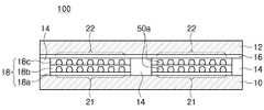
도 1을 참조하면 본 개시의 일 실시 예에 따른 박막형 코일 부품(100)은 기판(10); 상기 기판의 상부에 배치된 코일패턴(21, 22, 50a); 상기 코일패턴(21, 22, 50a)의 단면은 상단면 및 하단면 사이에 위치한 내부 영역 중 적어도 일 영역이 상기 상단면 및 하단면의 폭보다 큰 형상인 것을 만족한다.
Referring to Figure 1, a thin
상기 기판(10)은 자성체 기판일 수 있다. 상기 기판(10)상에 절연층(18)이 배치된다.The
구체적으로, 상기 박막형 코일 부품(100)는 상기 기판(10)상에 제1 절연층(18a), 상기 제1 절연층(18a)상에 배치된 제2 절연층(18b), 상기 제2 절연층(18b) 내에 형성된 코일패턴(21), 상기 제2 절연층(18b)상에 배치된 제3 절연층(18c), 상기 제3 절연층(18c) 내에 형성된 코일패턴(22) 순으로 적층된 구조를 가질 수 있다. 또한, 상기 박막형 코일 부품은 상기 적층된 코일패턴 상에 배치된 접착층(16) 및 상기 접착층(16) 상에 배치된 기판(12)을 포함하며, 상기 코일패턴(21, 22)의 단부에는 자성층(14)이 형성된다.Specifically, the thin
상기 절연층(18)은 폴리이미드 또는 에폭시 수지일 수 있다.The
상기 기판(10)의 상부에 코일패턴(21, 22, 50a)이 형성되며, 상기 코일패턴(21, 22, 50a)은 금, 은, 백금, 구리, 니켈 및 팔라듐 중 적어도 하나 또는 이들의 합금을 포함할 수 있다.The
상기 코일패턴(21, 22, 50a)은 도전성을 부여할 수 있는 재료로 이루어지면 족하며, 상기 나열된 금속에 한정되는 것은 아니다The
상기 코일패턴(21, 22, 50a)의 단면은 적층방향으로 상단면, 하단면 및 상단면과 하단면의 사이에 배치된 일 영역으로 이루어진 단면형상을 가진다.
The end faces of the
자성재료로 이루어진 기판(10)에는 철(Fe) 성분이 함유될 수 있는데, 이때, 코일들 사이의 간격이 좁은 경우 이러한 철 등의 성분에 의하여 통전 현상이 유발될 수 있다.The
상기 박막형 코일 부품은 상기 기판(10)과 상기 코일패턴(21) 사이에 배치된 제1 절연층(18a)을 포함할 수 있다. 상기 제1 절연층(18a)는 상기 기판과 코일 기판의 절연하는 역할을 할 수 있다.
The thin film coil component may include a first
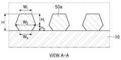
도 3은 본 개시의 일 실시 예에 따른 박막형 코일 부품의 코일패턴의 단면 형상을 도시한 것이다.3 illustrates a cross-sectional shape of a coil pattern of a thin film coil component according to an embodiment of the present disclosure.
도 3을 참조하면, 상기 코일패턴(50a)은 상단면 및 하단면 사이에 위치한 내부 영역 중 적어도 일 영역이 상기 상단면 및 하단면의 폭보다 큰 형상을 만족한다.Referring to FIG. 3, the
상기 코일패턴(50a)에서 상기 일 영역이 상기 상단면 및 하단면보다 폭이 크면, 코일패턴(50a)의 부피를 향상시켜 코일부품의 인덕턴스 및 저항 특성을 향상시킬 수 있다.
If the one area of the
복수의 코일패턴이 적층된 박막형 코일부품에서, 상하에 인접하는 코일패턴 간에 기생 커패시턴스(capacitance)가 발생할 수 있다. 이때 인접하는 코일패턴 간에 대응되는 면적을 감소시키면 기생 커패시턴스를 감소시킬 수 있다.In a thin film coil component in which a plurality of coil patterns are laminated, parasitic capacitance may occur between coil patterns adjacent to the upper and lower sides. At this time, if the area corresponding to the adjacent coil pattern is reduced, the parasitic capacitance can be reduced.
본 개시의 박막형 코일 부품의 코일패턴(50a)의 단면은 상단면이 하단면보다 폭이 작은 단면 형상을 가지며, 이로 인해 코일패턴 간의 발생하는 기생 커패시턴스를 감소시킬 수 있어 코일 부품의 전기적 손실을 감소시킬 수 있다.
The cross section of the
상기 코일패턴과 기판이 접촉되는 면인 하부의 면적이 너무 좁아지면 코일패턴이 기판에서 분리되는 현상이 발생할 수 있어 코일부품의 신뢰성이 저하될 수 있으며, 상기 코일패턴의 하단면의 면적이 너무 넓으면 코일패턴의 단면 및 부피가 오히려 감소되는 문제점이 발생할 수 있다.If the area of the lower portion of the coil pattern that is in contact with the substrate is too narrow, the coil pattern may be separated from the substrate, thereby reducing the reliability of the coil component. If the area of the lower end surface of the coil pattern is too wide The cross-section and the volume of the coil pattern may be rather reduced.
따라서, 상기 코일패턴(50a)의 단면은 상단면 및 하단면 사이에 위치한 내부 영역 중 적어도 일 영역이 상기 상단면 및 하단면의 폭보다 큰 형상을 만족함으로써, 기생 커패시턴스의 감소와 함께 인덕턴스 및 저항 특성을 향상시킬 수 있다.
Accordingly, the cross section of the
상기 코일패턴(50a)의 단면은 상기 코일패턴의 상단면에서 일 영역까지의 높이를 H1 및 하단면에서 일 영역까지의 높이를 H2라 할 때, H1>H2일 수 있다.The cross section of the
상기 코일패턴(50a)의 일 영역은 코일패턴의 전체 두께(H)에서 H1 및 H2의 두께로 분리되는 위치에 배치된다.One region of the
도 2를 참조하면, 상기 코일패턴(50a)의 단면은 하단면에 언터컷이 형성된 사다리꼴의 단면 형상을 가짐을 알 수 있다.
Referring to FIG. 2, the end face of the
인접하는 코일패턴은 절연성을 확보하기 위한 최소한의 이격 거리를 유지해야한다. 상기 코일패턴의 이격 거리가 작을수록 코일패턴의 부피가 증가될 수 있다.The adjacent coil pattern must maintain a minimum separation distance to ensure insulation. The smaller the spacing distance of the coil pattern is, the larger the volume of the coil pattern can be.
따라서, 상기 코일패턴(50a)의 간격은 상기 일 영역 폭의 0.15 내지 0.45배일 수 있으며, 상기 범위를 만족하는 범위에서 상기 코일패턴의 단면형상이 이루어질 수 있다.
Therefore, the interval of the
이하, 본 개시의 박막형 코일 부품의 제조방법에 대하여 설명한다.Hereinafter, a method of manufacturing the thin film coil component of the present disclosure will be described.
도 4a 내지 도 4f는 본 개시의 일 실시 예에 따른 박막형 코일 부품의 제조방법을 설명하기 위한 공정 단면도를 개략적으로 도시한 것이며, 도 3은 도 4f의 A부를 확대하여 도시한 것이다.FIGS. 4A to 4F are schematic sectional views of a process for explaining a method of manufacturing a thin film coil component according to an embodiment of the present disclosure, and FIG. 3 is an enlarged view of part A of FIG. 4F.
도 4a 내지 도 4f에 도시한 바와 같이, 본 개시의 일 실시 예에 따른 박막형 코일 부품의 제조방법은 기판(10) 표면에 금속 씨드층(20)을 형성하는 단계; 상기 금속 씨드층(20) 상에 포토레지스트 패턴(30)을 형성하는 단계; 상기 포토레지스트 패턴(30) 사이에 노출된 상기 금속 씨드층(20)의 표면에 금속을 도금하는 단계; 상기 포토레지스트 패턴(30)을 제거하여 제1 코일패턴(40, 41)을 형성하는 단계; 및 상기 제1 코일패턴(40, 41)을 에칭하여 제2 코일패턴(50a)을 형성하는 단계;를 포함한다.
As shown in FIGS. 4A to 4F, a method of manufacturing a thin film coil component according to an embodiment of the present disclosure includes: forming a
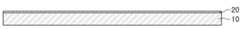
먼저, 도 4a 및 4b를 참조하면, 기판(10) 표면에 금속 씨드층(20)을 형성한다.First, referring to FIGS. 4A and 4B, a
상기 기판(10)은 자성체 기판일 수 있으며, 상기 금속 씨드층(20)은 후속 도금 공정을 수행하기 위한 씨드 물질을 스퍼터링(sputtering) 등의 방식으로 상기 기판(10)의 표면에 형성될 수 있다.
The
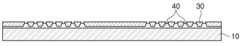
다음으로, 도 4c를 참조하면, 상기 금속 씨드층(20) 상에 포토레지스트 패턴(30)을 형성한다.Next, referring to FIG. 4C, a
상기 포토레지스트 패턴(30)은 네거티브 타입(negative type) 포토레지스트로 형성될 수 있다.The
상기 네거티브 타입 포토레지스트를 사용하면, 사다리꼴 단면 형상을 가지는 제1 코일패턴을 얻을 수 있다.When the negative type photoresist is used, a first coil pattern having a trapezoidal cross-sectional shape can be obtained.
상기 포토레지스트 패턴은 금속 씨드층 상에 도포한 후 도금될 영역을 제거함으로써 형성될 수 있다.
The photoresist pattern may be formed by applying a coating on the metal seed layer and then removing the region to be plated.
다음으로, 도 4d를 참조하면, 상기 포토레지스트 패턴(30) 사이에 노출된 상기 금속 씨드층(20)의 표면에 금속을 도금하여 도전재(40)를 형성할 수 있다.Next, referring to FIG. 4D, a
상기 금속은 금, 은, 백금, 구리, 니켈 및 팔라듐 중 적어도 하나 또는 이들의 합금을 포함할 수 있다.The metal may include at least one of gold, silver, platinum, copper, nickel, and palladium, or an alloy thereof.
상기 도금은 전해도금으로 수행될 수 있다.
The plating may be performed by electrolytic plating.
다음으로, 도 4e를 참조하면, 상기 포토레지스트 패턴(30)을 제거하여 제1 코일패턴(40, 41)을 형성한다.Next, referring to FIG. 4E, the
상기 제1 코일패턴(40, 41)은 상기 도전재(40)와 금속 씨드층(41)을 포함한다.
The
다음으로, 도 4f를 참조하면, 상기 제1 코일패턴(40, 41)을 에칭하여 제2 코일패턴(50a)을 형성한다.Next, referring to FIG. 4F, the
상기 제2 코일패턴(50a)은 제1 코일패턴(40, 41)에 과산화수소와 황산 등을 이용한 습식에칭(wet etching)하여 형성될 수 있다.The
상기 도금 공정이 과도하게 진행되어 코일패턴이 접촉되거나, 최소한의 이격 거리가 확보되지 않을 수 있으므로, 습식 에칭을 수행할 수 있다.The plating process may be excessively advanced so that the coil pattern may contact or the minimum separation distance may not be secured, so that wet etching can be performed.
상기 습식 에칭에 의하여 제2 코일패턴의 최소 이격거리를 확보할 수 있으며, 제2 코일패턴 사이의 쇼트가 발생하는 문제점을 방지할 수 있다.
The minimum etching distance of the second coil pattern can be ensured by the wet etching and the problem of short-circuiting between the second coil patterns can be prevented.
상기 제2 코일패턴(50a)의 단면은 습식 에칭으로 인하여 하부에 언더컷(undercut)을 가질 수 있다.The cross section of the
상기 제2 코일패턴(50a)의 단면 형상은 상단면 및 하단면 사이에 위치한 내부 영역 중 적어도 일 영역이 상기 상단면 및 하단면의 폭보다 큰 것을 만족한다.The cross-sectional shape of the
상기 제2 코일패턴(50a)에서 상기 일 영역이 상기 상단면 및 하단면보다 폭이 크면, 코일패턴의 부피를 향상시켜 코일부품의 인덕턴스 및 저항 특성을 향상시킬 수 있다.If the one area of the
상기 제2 코일패턴(50a)의 단면은 상단면이 하단면보다 폭이 작은 단면 형상을 가지며, 이로 인해 코일패턴 간의 발생하는 기생 커패시턴스를 감소시킬 수 있어 코일 부품의 전기적 손실을 감소시킬 수 있다.The end face of the
따라서, 상기 제2 코일패턴(50a)의 단면은 상단면 및 하단면 사이에 위치한 내부 영역 중 적어도 일 영역이 상기 상단면 및 하단면의 폭보다 큰 형상을 만족함으로써, 기생 커패시턴스의 감소와 함께 인덕턴스 및 저항 특성을 향상시킬 수 있다.
Therefore, the cross section of the
상기 제2 코일패턴(50a)은 상기 제2 코일패턴의 단면 형상에서 상단면에서 일 영역까지의 높이를 H1 및 하단면에서 일 영역까지의 높이를 H2라 할 때, H1>H2일 수 있다.The
상기 제2 코일패턴(50a)의 일 영역은 코일패턴의 전체 두께(H)에서 H1 및 H2의 두께로 분리되는 위치에 배치된다.One region of the
본 개시의 일 실시 예에 따른 박막형 코일 부품은 언더컷을 가지는 사다리꼴 단면 형상인 코일패턴을 가지며, 이로 인해 코일패턴 사이에 발생하는 기생 커패시턴스를 최소화할 수 있어 전기적 손실을 줄일 수 있으며, 코일패턴의 부피를 증가시켜 인덕턴스 및 저항 특성을 향상시킬 수 있다.
The thin film coil component according to an embodiment of the present disclosure has a coil pattern having a trapezoidal cross-sectional shape with an undercut, thereby minimizing the parasitic capacitance generated between the coil patterns, thereby reducing the electrical loss, The inductance and resistance characteristics can be improved.
본 개시는 상술한 실시형태 및 첨부된 도면에 의해 제한되는 것이 아니며 첨부된 청구범위에 의해 제한하고자 한다.The present disclosure is not limited by the above-described embodiments and the accompanying drawings, but is intended to be limited by the appended claims.
따라서, 청구범위에 기재된 본 개시의 기술적 사상을 벗어나지 않는 범위 내에서 당 기술분야의 통상의 지식을 가진 자에 의해 다양한 형태의 치환, 변형 및 변경이 가능할 것이며, 이 또한 본 개시의 범위에 속한다고 할 것이다.
Accordingly, various modifications, substitutions, and alterations can be made by those skilled in the art without departing from the spirit of the present disclosure, which is also within the scope of the present disclosure something to do.
10, 12: 기판
14: 자성층
16: 접착층
18: 절연막
20: 금속 씨드층
21, 22, 50a: 코일패턴
30: 포토레지스트 패턴
40: 도전재10, 12: substrate
14: magnetic layer
16:
18: Insulating film
20: metal seed layer
21, 22, 50a: Coil pattern
30: Photoresist pattern
40: conductive material
Claims (16)
Translated fromKorean상기 기판의 상부에 배치된 코일패턴;
상기 코일패턴의 단면은 상단면 및 하단면 사이에 위치한 내부 영역 중 적어도 일 영역이 상기 상단면 및 하단면의 폭보다 큰 형상인 박막형 코일 부품.
Board;
A coil pattern disposed on the substrate;
Wherein a cross section of the coil pattern has a shape in which at least one region of an inner region located between an upper end surface and a lower end surface is larger than a width of the upper end surface and the lower end surface.
상기 코일패턴의 단면은 상단면에서 상기 일 영역까지의 높이를 H1 및 상기 하단면에서 상기 일 영역까지의 높이를 H2라 할 때, H1>H2인 박막형 코일 부품.
The method according to claim 1,
Wherein a cross-section of the coil pattern is H1 > H2 when the height from the top surface to the one region is H1 and the height from the bottom surface to the one region is H2.
상기 코일패턴의 간격은 상기 일 영역의 폭의 0.15 내지 0.45배인 박막형 코일 부품.
The method according to claim 1,
Wherein the interval of the coil patterns is 0.15 to 0.45 times the width of the one region.
상기 코일패턴은 금, 은, 백금, 구리, 니켈 및 팔라듐 중 적어도 하나 또는 이들의 합금을 포함하는 박막형 코일 부품.
The method according to claim 1,
Wherein the coil pattern comprises at least one of gold, silver, platinum, copper, nickel, and palladium or an alloy thereof.
상기 기판은 자성체 기판인 박막형 코일 부품.
The method according to claim 1,
Wherein the substrate is a magnetic substrate.
상기 기판상에 배치된 절연층;을 포함하는 박막형 코일 부품.
The method according to claim 1,
And an insulating layer disposed on the substrate.
상기 코일패턴의 단면은 하단면에 언터컷이 형성된 사다리꼴의 단면 형상을 가지는 박막형 코일 부품.
The method according to claim 6,
Sectional shape of the coil pattern has a trapezoidal cross-sectional shape in which an undersurface is formed on the lower end surface.
상기 코일패턴은 상기 절연층 내에 배치되는 박막형 코일 부품.
The method according to claim 6,
Wherein the coil pattern is disposed in the insulating layer.
상기 금속 씨드층 상에 포토레지스트 패턴을 형성하는 단계;
상기 포토레지스트 패턴 사이에 노출된 상기 금속 씨드층의 표면에 금속을 도금하는 단계;
상기 포토레지스트 패턴을 제거하여 제1 코일패턴을 형성하는 단계; 및
상기 제1 코일패턴을 에칭하여 제2 코일패턴을 형성하는 단계;를 포함하는 박막형 코일 부품의 제조방법.
Forming a metal seed layer on the substrate surface;
Forming a photoresist pattern on the metal seed layer;
Plating a metal on the surface of the metal seed layer exposed between the photoresist patterns;
Removing the photoresist pattern to form a first coil pattern; And
And etching the first coil pattern to form a second coil pattern.
상기 제2 코일패턴의 단면은 하부에 언더컷(undercut)을 가지는 박막형 코일 부품의 제조방법.
10. The method of claim 9,
And a cross section of the second coil pattern has an undercut in an undercut.
상기 제2 코일패턴의 단면은 상단면 및 하단면 사이에 위치한 내부 영역 중 적어도 일 영역이 상기 상단면 및 하단면의 폭보다 큰 형상인 박막형 코일 부품의 제조방법.
10. The method of claim 9,
Wherein a cross section of the second coil pattern has a shape in which at least one region of the inner region located between the upper end surface and the lower end surface is larger than the width of the upper end surface and the lower end surface.
상기 제2 코일패턴의 단면은 상단면에서 일 영역까지의 높이를 H1 및 하단면에서 일 영역까지의 높이를 H2라 할 때, H1>H2인 박막형 코일 부품의 제조방법.
10. The method of claim 9,
Wherein a section of the second coil pattern has a height H1 from the top surface to one region and a height H2 to one region from the bottom surface to H1> H2.
상기 도금하는 단계에서, 상기 금속은 금, 은, 백금, 구리, 니켈 및 팔라듐 중 적어도 하나 또는 이들의 합금을 포함하는 박막형 코일 부품의 제조방법.
10. The method of claim 9,
Wherein the metal comprises at least one of gold, silver, platinum, copper, nickel, and palladium or an alloy thereof in the plating step.
상기 도금하는 단계는 전해도금으로 수행되는 박막형 코일 부품의 제조방법.
10. The method of claim 9,
Wherein the plating is performed by electrolytic plating.
상기 포토레지스트 패턴은 네거티브 타입(negative type) 포토레지스트로 형성되는 박막형 코일 부품의 제조방법.
10. The method of claim 9,
Wherein the photoresist pattern is formed of a negative type photoresist.
상기 제2 코일패턴은 제1 코일패턴을 습식 에칭하여 형성되는 박막형 코일 부품의 제조방법.
10. The method of claim 9,
Wherein the second coil pattern is formed by wet-etching the first coil pattern.
Priority Applications (2)
| Application Number | Priority Date | Filing Date | Title |
|---|---|---|---|
| KR1020150093569AKR20170003199A (en) | 2015-06-30 | 2015-06-30 | Thin film type coil component and method of manufacturing the same |
| US14/989,713US10026539B2 (en) | 2015-06-30 | 2016-01-06 | Thin film type coil component and method of manufacturing the same |
Applications Claiming Priority (1)
| Application Number | Priority Date | Filing Date | Title |
|---|---|---|---|
| KR1020150093569AKR20170003199A (en) | 2015-06-30 | 2015-06-30 | Thin film type coil component and method of manufacturing the same |
Publications (1)
| Publication Number | Publication Date |
|---|---|
| KR20170003199Atrue KR20170003199A (en) | 2017-01-09 |
Family
ID=57684022
Family Applications (1)
| Application Number | Title | Priority Date | Filing Date |
|---|---|---|---|
| KR1020150093569ACeasedKR20170003199A (en) | 2015-06-30 | 2015-06-30 | Thin film type coil component and method of manufacturing the same |
Country Status (2)
| Country | Link |
|---|---|
| US (1) | US10026539B2 (en) |
| KR (1) | KR20170003199A (en) |
Families Citing this family (6)
| Publication number | Priority date | Publication date | Assignee | Title |
|---|---|---|---|---|
| CN209747274U (en)* | 2017-03-01 | 2019-12-06 | 株式会社村田制作所 | Mounting substrates, electrical components, vibration plates, and electrical components |
| CN107705971A (en)* | 2017-08-30 | 2018-02-16 | 歌尔股份有限公司 | A kind of manufacture method of coil, coil, electronic equipment |
| KR102505437B1 (en)* | 2017-12-26 | 2023-03-03 | 삼성전기주식회사 | Wire wound inductor and manufacturing method thereof |
| JP6962284B2 (en)* | 2018-07-17 | 2021-11-05 | 株式会社村田製作所 | Inductor parts |
| US11031244B2 (en)* | 2018-08-14 | 2021-06-08 | Lam Research Corporation | Modification of SNO2 surface for EUV lithography |
| KR20220099006A (en)* | 2021-01-05 | 2022-07-12 | 삼성전기주식회사 | Coil component |
Citations (2)
| Publication number | Priority date | Publication date | Assignee | Title |
|---|---|---|---|---|
| JP2006332147A (en) | 2005-05-24 | 2006-12-07 | Matsushita Electric Ind Co Ltd | Coil conductor, method for manufacturing the same, and method for manufacturing a coil component using the same |
| KR20130104808A (en) | 2012-03-15 | 2013-09-25 | 삼성전기주식회사 | Method for manufacturing common mode filter and common mode filter |
Family Cites Families (11)
| Publication number | Priority date | Publication date | Assignee | Title |
|---|---|---|---|---|
| US6600404B1 (en)* | 1998-01-12 | 2003-07-29 | Tdk Corporation | Planar coil and planar transformer, and process of fabricating a high-aspect conductive device |
| JP2001244123A (en)* | 2000-02-28 | 2001-09-07 | Kawatetsu Mining Co Ltd | Surface mount type planar magnetic element and method of manufacturing the same |
| EP1708209A4 (en)* | 2004-01-23 | 2014-11-12 | Murata Manufacturing Co | Chip inductor and process for producing the same |
| JP4293603B2 (en)* | 2004-02-25 | 2009-07-08 | Tdk株式会社 | Coil component and manufacturing method thereof |
| JP4012526B2 (en)* | 2004-07-01 | 2007-11-21 | Tdk株式会社 | Thin film coil and manufacturing method thereof, and coil structure and manufacturing method thereof |
| WO2006057115A1 (en)* | 2004-11-25 | 2006-06-01 | Murata Manufacturing Co., Ltd. | Coil component |
| JP2006286931A (en)* | 2005-03-31 | 2006-10-19 | Tdk Corp | Thin film device |
| JP2007266105A (en)* | 2006-03-27 | 2007-10-11 | Tdk Corp | Thin-film device |
| JP5962754B2 (en)* | 2012-03-27 | 2016-08-03 | 株式会社村田製作所 | Electronic components |
| KR101792281B1 (en)* | 2012-12-14 | 2017-11-01 | 삼성전기주식회사 | Power Inductor and Manufacturing Method for the Same |
| KR20150035280A (en)* | 2013-09-27 | 2015-04-06 | 삼성전기주식회사 | coil sheet and manufacturing method of the same |
- 2015
- 2015-06-30KRKR1020150093569Apatent/KR20170003199A/ennot_activeCeased
- 2016
- 2016-01-06USUS14/989,713patent/US10026539B2/enactiveActive
Patent Citations (2)
| Publication number | Priority date | Publication date | Assignee | Title |
|---|---|---|---|---|
| JP2006332147A (en) | 2005-05-24 | 2006-12-07 | Matsushita Electric Ind Co Ltd | Coil conductor, method for manufacturing the same, and method for manufacturing a coil component using the same |
| KR20130104808A (en) | 2012-03-15 | 2013-09-25 | 삼성전기주식회사 | Method for manufacturing common mode filter and common mode filter |
Also Published As
| Publication number | Publication date |
|---|---|
| US20170004917A1 (en) | 2017-01-05 |
| US10026539B2 (en) | 2018-07-17 |
Similar Documents
| Publication | Publication Date | Title |
|---|---|---|
| KR102163415B1 (en) | Coil component and method of manufacturing the same | |
| KR20170003199A (en) | Thin film type coil component and method of manufacturing the same | |
| KR101514499B1 (en) | Method for manufacturing common mode filter and common mode filter | |
| KR102642913B1 (en) | Multilayered electronic component and manufacturing method thereof | |
| KR102680004B1 (en) | Inductor | |
| US9741490B2 (en) | Power inductor and manufacturing method thereof | |
| KR102016490B1 (en) | Coil Component | |
| CN110544574B (en) | Coil electronic component | |
| US9173291B2 (en) | Circuit board and method for manufacturing the same | |
| US20160071643A1 (en) | Coil unit for power inductor, manufacturing method of coil unit for power inductor, power inductor and manufacturing method of power inductor | |
| KR20190000606A (en) | Thin film type inductor | |
| KR20150035280A (en) | coil sheet and manufacturing method of the same | |
| US20140102770A1 (en) | Core substrate, manufacturing method thereof, and structure for metal via | |
| US10984942B2 (en) | Coil component | |
| JP7334558B2 (en) | inductor components | |
| KR101973449B1 (en) | Inductor | |
| KR20200069626A (en) | Coil electronic component | |
| KR101792272B1 (en) | Semiconductor substrate and method for producing semiconductor substrate | |
| US12424375B2 (en) | Coil electronic component | |
| KR102186153B1 (en) | Chip electronic component and manufacturing method thereof | |
| KR20200052595A (en) | Coil electronic component | |
| KR20140067360A (en) | Power inductor with high inductance and manufacturing method thereof | |
| CN110739132A (en) | Coil assembly and method of manufacturing the same | |
| CN102983121A (en) | Manufacturing method and structure of three-dimensional inductive carrier with metal core | |
| JP2011176067A (en) | Solid-state electrolytic capacitor |
Legal Events
| Date | Code | Title | Description |
|---|---|---|---|
| PA0109 | Patent application | Patent event code:PA01091R01D Comment text:Patent Application Patent event date:20150630 | |
| PG1501 | Laying open of application | ||
| PA0201 | Request for examination | Patent event code:PA02012R01D Patent event date:20181129 Comment text:Request for Examination of Application Patent event code:PA02011R01I Patent event date:20150630 Comment text:Patent Application | |
| E902 | Notification of reason for refusal | ||
| PE0902 | Notice of grounds for rejection | Comment text:Notification of reason for refusal Patent event date:20191217 Patent event code:PE09021S01D | |
| AMND | Amendment | ||
| E601 | Decision to refuse application | ||
| PE0601 | Decision on rejection of patent | Patent event date:20200220 Comment text:Decision to Refuse Application Patent event code:PE06012S01D Patent event date:20191217 Comment text:Notification of reason for refusal Patent event code:PE06011S01I | |
| AMND | Amendment | ||
| PX0901 | Re-examination | Patent event code:PX09011S01I Patent event date:20200220 Comment text:Decision to Refuse Application Patent event code:PX09012R01I Patent event date:20200211 Comment text:Amendment to Specification, etc. | |
| PX0601 | Decision of rejection after re-examination | Comment text:Decision to Refuse Application Patent event code:PX06014S01D Patent event date:20200407 Comment text:Amendment to Specification, etc. Patent event code:PX06012R01I Patent event date:20200317 Comment text:Decision to Refuse Application Patent event code:PX06011S01I Patent event date:20200220 Comment text:Amendment to Specification, etc. Patent event code:PX06012R01I Patent event date:20200211 Comment text:Notification of reason for refusal Patent event code:PX06013S01I Patent event date:20191217 | |
| X601 | Decision of rejection after re-examination |