KR20170002764A - Method of fabricating semiconductor device - Google Patents
Method of fabricating semiconductor deviceDownload PDFInfo
- Publication number
- KR20170002764A KR20170002764AKR1020150092375AKR20150092375AKR20170002764AKR 20170002764 AKR20170002764 AKR 20170002764AKR 1020150092375 AKR1020150092375 AKR 1020150092375AKR 20150092375 AKR20150092375 AKR 20150092375AKR 20170002764 AKR20170002764 AKR 20170002764A
- Authority
- KR
- South Korea
- Prior art keywords
- etchant
- etching
- etchants
- stack structure
- material layer
- Prior art date
- Legal status (The legal status is an assumption and is not a legal conclusion. Google has not performed a legal analysis and makes no representation as to the accuracy of the status listed.)
- Ceased
Links
Images


Classifications
- H—ELECTRICITY
- H01—ELECTRIC ELEMENTS
- H01L—SEMICONDUCTOR DEVICES NOT COVERED BY CLASS H10
- H01L21/00—Processes or apparatus adapted for the manufacture or treatment of semiconductor or solid state devices or of parts thereof
- H01L21/70—Manufacture or treatment of devices consisting of a plurality of solid state components formed in or on a common substrate or of parts thereof; Manufacture of integrated circuit devices or of parts thereof
- H01L21/71—Manufacture of specific parts of devices defined in group H01L21/70
- H01L21/768—Applying interconnections to be used for carrying current between separate components within a device comprising conductors and dielectrics
- H01L21/76801—Applying interconnections to be used for carrying current between separate components within a device comprising conductors and dielectrics characterised by the formation and the after-treatment of the dielectrics, e.g. smoothing
- H01L21/76802—Applying interconnections to be used for carrying current between separate components within a device comprising conductors and dielectrics characterised by the formation and the after-treatment of the dielectrics, e.g. smoothing by forming openings in dielectrics
- H01L21/76807—Applying interconnections to be used for carrying current between separate components within a device comprising conductors and dielectrics characterised by the formation and the after-treatment of the dielectrics, e.g. smoothing by forming openings in dielectrics for dual damascene structures
- H01L21/76811—Applying interconnections to be used for carrying current between separate components within a device comprising conductors and dielectrics characterised by the formation and the after-treatment of the dielectrics, e.g. smoothing by forming openings in dielectrics for dual damascene structures involving multiple stacked pre-patterned masks
- H—ELECTRICITY
- H01—ELECTRIC ELEMENTS
- H01L—SEMICONDUCTOR DEVICES NOT COVERED BY CLASS H10
- H01L22/00—Testing or measuring during manufacture or treatment; Reliability measurements, i.e. testing of parts without further processing to modify the parts as such; Structural arrangements therefor
- H01L22/20—Sequence of activities consisting of a plurality of measurements, corrections, marking or sorting steps
- H01L22/26—Acting in response to an ongoing measurement without interruption of processing, e.g. endpoint detection, in-situ thickness measurement
- H—ELECTRICITY
- H01—ELECTRIC ELEMENTS
- H01J—ELECTRIC DISCHARGE TUBES OR DISCHARGE LAMPS
- H01J37/00—Discharge tubes with provision for introducing objects or material to be exposed to the discharge, e.g. for the purpose of examination or processing thereof
- H01J37/32—Gas-filled discharge tubes
- H01J37/32917—Plasma diagnostics
- H01J37/32935—Monitoring and controlling tubes by information coming from the object and/or discharge
- H01J37/32963—End-point detection
- H—ELECTRICITY
- H01—ELECTRIC ELEMENTS
- H01L—SEMICONDUCTOR DEVICES NOT COVERED BY CLASS H10
- H01L21/00—Processes or apparatus adapted for the manufacture or treatment of semiconductor or solid state devices or of parts thereof
- H01L21/02—Manufacture or treatment of semiconductor devices or of parts thereof
- H01L21/04—Manufacture or treatment of semiconductor devices or of parts thereof the devices having potential barriers, e.g. a PN junction, depletion layer or carrier concentration layer
- H01L21/18—Manufacture or treatment of semiconductor devices or of parts thereof the devices having potential barriers, e.g. a PN junction, depletion layer or carrier concentration layer the devices having semiconductor bodies comprising elements of Group IV of the Periodic Table or AIIIBV compounds with or without impurities, e.g. doping materials
- H01L21/28—Manufacture of electrodes on semiconductor bodies using processes or apparatus not provided for in groups H01L21/20 - H01L21/268
- H01L21/28008—Making conductor-insulator-semiconductor electrodes
- H—ELECTRICITY
- H01—ELECTRIC ELEMENTS
- H01L—SEMICONDUCTOR DEVICES NOT COVERED BY CLASS H10
- H01L21/00—Processes or apparatus adapted for the manufacture or treatment of semiconductor or solid state devices or of parts thereof
- H01L21/02—Manufacture or treatment of semiconductor devices or of parts thereof
- H01L21/04—Manufacture or treatment of semiconductor devices or of parts thereof the devices having potential barriers, e.g. a PN junction, depletion layer or carrier concentration layer
- H01L21/18—Manufacture or treatment of semiconductor devices or of parts thereof the devices having potential barriers, e.g. a PN junction, depletion layer or carrier concentration layer the devices having semiconductor bodies comprising elements of Group IV of the Periodic Table or AIIIBV compounds with or without impurities, e.g. doping materials
- H01L21/30—Treatment of semiconductor bodies using processes or apparatus not provided for in groups H01L21/20 - H01L21/26
- H01L21/302—Treatment of semiconductor bodies using processes or apparatus not provided for in groups H01L21/20 - H01L21/26 to change their surface-physical characteristics or shape, e.g. etching, polishing, cutting
- H01L21/306—Chemical or electrical treatment, e.g. electrolytic etching
- H01L21/3065—Plasma etching; Reactive-ion etching
- H—ELECTRICITY
- H01—ELECTRIC ELEMENTS
- H01L—SEMICONDUCTOR DEVICES NOT COVERED BY CLASS H10
- H01L21/00—Processes or apparatus adapted for the manufacture or treatment of semiconductor or solid state devices or of parts thereof
- H01L21/02—Manufacture or treatment of semiconductor devices or of parts thereof
- H01L21/04—Manufacture or treatment of semiconductor devices or of parts thereof the devices having potential barriers, e.g. a PN junction, depletion layer or carrier concentration layer
- H01L21/18—Manufacture or treatment of semiconductor devices or of parts thereof the devices having potential barriers, e.g. a PN junction, depletion layer or carrier concentration layer the devices having semiconductor bodies comprising elements of Group IV of the Periodic Table or AIIIBV compounds with or without impurities, e.g. doping materials
- H01L21/30—Treatment of semiconductor bodies using processes or apparatus not provided for in groups H01L21/20 - H01L21/26
- H01L21/31—Treatment of semiconductor bodies using processes or apparatus not provided for in groups H01L21/20 - H01L21/26 to form insulating layers thereon, e.g. for masking or by using photolithographic techniques; After treatment of these layers; Selection of materials for these layers
- H01L21/3105—After-treatment
- H01L21/311—Etching the insulating layers by chemical or physical means
- H01L21/31105—Etching inorganic layers
- H01L21/31111—Etching inorganic layers by chemical means
- H01L21/31116—Etching inorganic layers by chemical means by dry-etching
- H—ELECTRICITY
- H01—ELECTRIC ELEMENTS
- H01L—SEMICONDUCTOR DEVICES NOT COVERED BY CLASS H10
- H01L21/00—Processes or apparatus adapted for the manufacture or treatment of semiconductor or solid state devices or of parts thereof
- H01L21/02—Manufacture or treatment of semiconductor devices or of parts thereof
- H01L21/04—Manufacture or treatment of semiconductor devices or of parts thereof the devices having potential barriers, e.g. a PN junction, depletion layer or carrier concentration layer
- H01L21/18—Manufacture or treatment of semiconductor devices or of parts thereof the devices having potential barriers, e.g. a PN junction, depletion layer or carrier concentration layer the devices having semiconductor bodies comprising elements of Group IV of the Periodic Table or AIIIBV compounds with or without impurities, e.g. doping materials
- H01L21/30—Treatment of semiconductor bodies using processes or apparatus not provided for in groups H01L21/20 - H01L21/26
- H01L21/31—Treatment of semiconductor bodies using processes or apparatus not provided for in groups H01L21/20 - H01L21/26 to form insulating layers thereon, e.g. for masking or by using photolithographic techniques; After treatment of these layers; Selection of materials for these layers
- H01L21/3205—Deposition of non-insulating-, e.g. conductive- or resistive-, layers on insulating layers; After-treatment of these layers
- H01L21/321—After treatment
- H01L21/3213—Physical or chemical etching of the layers, e.g. to produce a patterned layer from a pre-deposited extensive layer
- H01L21/32133—Physical or chemical etching of the layers, e.g. to produce a patterned layer from a pre-deposited extensive layer by chemical means only
- H01L21/32135—Physical or chemical etching of the layers, e.g. to produce a patterned layer from a pre-deposited extensive layer by chemical means only by vapour etching only
- H—ELECTRICITY
- H01—ELECTRIC ELEMENTS
- H01L—SEMICONDUCTOR DEVICES NOT COVERED BY CLASS H10
- H01L21/00—Processes or apparatus adapted for the manufacture or treatment of semiconductor or solid state devices or of parts thereof
- H01L21/70—Manufacture or treatment of devices consisting of a plurality of solid state components formed in or on a common substrate or of parts thereof; Manufacture of integrated circuit devices or of parts thereof
- H01L21/71—Manufacture of specific parts of devices defined in group H01L21/70
- H01L21/768—Applying interconnections to be used for carrying current between separate components within a device comprising conductors and dielectrics
- H01L21/76801—Applying interconnections to be used for carrying current between separate components within a device comprising conductors and dielectrics characterised by the formation and the after-treatment of the dielectrics, e.g. smoothing
- H01L21/76802—Applying interconnections to be used for carrying current between separate components within a device comprising conductors and dielectrics characterised by the formation and the after-treatment of the dielectrics, e.g. smoothing by forming openings in dielectrics
- H01L21/76807—Applying interconnections to be used for carrying current between separate components within a device comprising conductors and dielectrics characterised by the formation and the after-treatment of the dielectrics, e.g. smoothing by forming openings in dielectrics for dual damascene structures
- H01L21/76813—Applying interconnections to be used for carrying current between separate components within a device comprising conductors and dielectrics characterised by the formation and the after-treatment of the dielectrics, e.g. smoothing by forming openings in dielectrics for dual damascene structures involving a partial via etch
- H—ELECTRICITY
- H01—ELECTRIC ELEMENTS
- H01L—SEMICONDUCTOR DEVICES NOT COVERED BY CLASS H10
- H01L21/00—Processes or apparatus adapted for the manufacture or treatment of semiconductor or solid state devices or of parts thereof
- H01L21/70—Manufacture or treatment of devices consisting of a plurality of solid state components formed in or on a common substrate or of parts thereof; Manufacture of integrated circuit devices or of parts thereof
- H01L21/71—Manufacture of specific parts of devices defined in group H01L21/70
- H01L21/768—Applying interconnections to be used for carrying current between separate components within a device comprising conductors and dielectrics
- H01L21/76801—Applying interconnections to be used for carrying current between separate components within a device comprising conductors and dielectrics characterised by the formation and the after-treatment of the dielectrics, e.g. smoothing
- H01L21/76829—Applying interconnections to be used for carrying current between separate components within a device comprising conductors and dielectrics characterised by the formation and the after-treatment of the dielectrics, e.g. smoothing characterised by the formation of thin functional dielectric layers, e.g. dielectric etch-stop, barrier, capping or liner layers
- H01L21/76832—Multiple layers
- H—ELECTRICITY
- H01—ELECTRIC ELEMENTS
- H01L—SEMICONDUCTOR DEVICES NOT COVERED BY CLASS H10
- H01L21/00—Processes or apparatus adapted for the manufacture or treatment of semiconductor or solid state devices or of parts thereof
- H01L21/70—Manufacture or treatment of devices consisting of a plurality of solid state components formed in or on a common substrate or of parts thereof; Manufacture of integrated circuit devices or of parts thereof
- H01L21/71—Manufacture of specific parts of devices defined in group H01L21/70
- H01L21/768—Applying interconnections to be used for carrying current between separate components within a device comprising conductors and dielectrics
- H01L21/76838—Applying interconnections to be used for carrying current between separate components within a device comprising conductors and dielectrics characterised by the formation and the after-treatment of the conductors
- H01L21/76841—Barrier, adhesion or liner layers
- H01L21/76853—Barrier, adhesion or liner layers characterized by particular after-treatment steps
- H01L21/76855—After-treatment introducing at least one additional element into the layer
- H01L21/76856—After-treatment introducing at least one additional element into the layer by treatment in plasmas or gaseous environments, e.g. nitriding a refractory metal liner
- H—ELECTRICITY
- H10—SEMICONDUCTOR DEVICES; ELECTRIC SOLID-STATE DEVICES NOT OTHERWISE PROVIDED FOR
- H10B—ELECTRONIC MEMORY DEVICES
- H10B43/00—EEPROM devices comprising charge-trapping gate insulators
- H10B43/20—EEPROM devices comprising charge-trapping gate insulators characterised by three-dimensional arrangements, e.g. with cells on different height levels
- H10B43/23—EEPROM devices comprising charge-trapping gate insulators characterised by three-dimensional arrangements, e.g. with cells on different height levels with source and drain on different levels, e.g. with sloping channels
- H10B43/27—EEPROM devices comprising charge-trapping gate insulators characterised by three-dimensional arrangements, e.g. with cells on different height levels with source and drain on different levels, e.g. with sloping channels the channels comprising vertical portions, e.g. U-shaped channels
- H—ELECTRICITY
- H01—ELECTRIC ELEMENTS
- H01J—ELECTRIC DISCHARGE TUBES OR DISCHARGE LAMPS
- H01J2237/00—Discharge tubes exposing object to beam, e.g. for analysis treatment, etching, imaging
- H01J2237/32—Processing objects by plasma generation
- H01J2237/33—Processing objects by plasma generation characterised by the type of processing
- H01J2237/334—Etching
- H—ELECTRICITY
- H01—ELECTRIC ELEMENTS
- H01L—SEMICONDUCTOR DEVICES NOT COVERED BY CLASS H10
- H01L22/00—Testing or measuring during manufacture or treatment; Reliability measurements, i.e. testing of parts without further processing to modify the parts as such; Structural arrangements therefor
- H01L22/10—Measuring as part of the manufacturing process
- H01L22/12—Measuring as part of the manufacturing process for structural parameters, e.g. thickness, line width, refractive index, temperature, warp, bond strength, defects, optical inspection, electrical measurement of structural dimensions, metallurgic measurement of diffusions
- H—ELECTRICITY
- H10—SEMICONDUCTOR DEVICES; ELECTRIC SOLID-STATE DEVICES NOT OTHERWISE PROVIDED FOR
- H10B—ELECTRONIC MEMORY DEVICES
- H10B41/00—Electrically erasable-and-programmable ROM [EEPROM] devices comprising floating gates
- H10B41/20—Electrically erasable-and-programmable ROM [EEPROM] devices comprising floating gates characterised by three-dimensional arrangements, e.g. with cells on different height levels
- H10B41/23—Electrically erasable-and-programmable ROM [EEPROM] devices comprising floating gates characterised by three-dimensional arrangements, e.g. with cells on different height levels with source and drain on different levels, e.g. with sloping channels
- H10B41/27—Electrically erasable-and-programmable ROM [EEPROM] devices comprising floating gates characterised by three-dimensional arrangements, e.g. with cells on different height levels with source and drain on different levels, e.g. with sloping channels the channels comprising vertical portions, e.g. U-shaped channels
Landscapes
- Engineering & Computer Science (AREA)
- Physics & Mathematics (AREA)
- Power Engineering (AREA)
- Manufacturing & Machinery (AREA)
- Computer Hardware Design (AREA)
- Microelectronics & Electronic Packaging (AREA)
- Chemical & Material Sciences (AREA)
- General Physics & Mathematics (AREA)
- Condensed Matter Physics & Semiconductors (AREA)
- Chemical Kinetics & Catalysis (AREA)
- General Chemical & Material Sciences (AREA)
- Plasma & Fusion (AREA)
- Inorganic Chemistry (AREA)
- Analytical Chemistry (AREA)
- Drying Of Semiconductors (AREA)
Abstract
Translated fromKoreanDescription
Translated fromKorean본 발명은 반도체 소자의 제조 방법에 관련된 것으로, 더욱 상세하게는 신뢰성이 보다 향상된 반도체 소자의 제조 방법에 관련된 것이다.BACKGROUND OF THE
소형화, 다기능화 및/또는 낮은 제조 단가 등의 특성들로 인하여 반도체 소자는 전자 산업에서 널리 사용되고 있다. 하지만, 전자 사업의 발전과 함께 반도체 소자는 점점 더 고집적화 되고 있어, 여러 문제점들을 야기시키고 있다. 예컨대, 반도체 소자의 고집적화에 의해 반도체 소자 내 패턴들의 선폭 및/또는 간격이 감소되는 반면에 상기 패턴들의 높이 및/또는 종횡비가 증가되고 있다. 이에 따라, 박막들의 증착 공정 및/또는 식각 공정의 산포가 점점 나빠져, 반도체 소자의 신뢰성이 저하되고 있다.Semiconductor devices are widely used in the electronics industry due to their small size, versatility and / or low manufacturing cost. However, with the development of electronic business, semiconductor devices are becoming more and more highly integrated, causing many problems. For example, the height and / or aspect ratio of the patterns are increasing while the line width and / or spacing of the patterns in the semiconductor elements are reduced by the high integration of the semiconductor elements. As a result, the deposition process of the thin films and / or the scattering of the etching process is getting worse and the reliability of the semiconductor device is lowered.
본 발명이 이루고자 하는 일 기술적 과제는 향상된 신뢰성을 가지며 보다 고집적화된 반도체 소자를 제조하는 방법을 제공하는데 있다.SUMMARY OF THE INVENTION It is an object of the present invention to provide a method of manufacturing a highly integrated semiconductor device having improved reliability.
본 발명이 해결하고자 하는 과제는 이상에서 언급한 과제에 제한되지 않으며, 언급되지 않은 또 다른 과제들은 아래의 기재로부터 당업자에게 명확하게 이해될 수 있을 것이다.The problems to be solved by the present invention are not limited to the above-mentioned problems, and other problems not mentioned can be clearly understood by those skilled in the art from the following description.
본 발명의 개념에 따른 일 실시예는 반도체 소자의 제조 방법을 제공한다. 상기 반도체 소자의 제조 방법은, 기판 상에, 제1 에천트로 식각되는 제1 물질막들 및 제2 에천트로 식각되는 제2 물질막들이 교번하여 적층된 스택 구조물을 형성하고; 상기 스택 구조물 상에 마스크 패턴을 형성하고; 상기 마스크 패턴을 이용하여 상기 스택 구조물의 상부를 제1 공정으로 식각하여 개구를 형성하고; 및 상기 마스크 패턴을 이용하여 상기 스택 구조물의 하부를 제2 공정으로 식각하여 상기 기판을 노출시키도록 상기 개구를 확장하되, 상기 제1 공정은, 상기 식각 공정으로 발생되는 제1 및 제2 식각 반응 가스들의 EPD 신호를 이용하여 상기 제1 및 제2 에천트들을 변경하여 상기 상부의 제1 및 제2 물질막들을 식각하는 것을 포함하고, 상기 제1 공정을 수행하는 동안 상기 개구의 깊이에 대한 상기 제1 및 제2 에천트들의 주입 시간 함수를 획득하며, 상기 제2 공정은, 상기 획득된 함수를 이용하여 상기 제1 및 제2 에천트들을 변경하여, 상기 하부의 제1 및 제2 물질막들을 식각하는 것을 포함한다.One embodiment according to the concept of the present invention provides a method of manufacturing a semiconductor device. The method of manufacturing a semiconductor device includes forming a stack structure on a substrate by alternately stacking first material films etched by a first etchant and second material films etched by a second etchant; Forming a mask pattern on the stack structure; Etching the upper portion of the stack structure using the mask pattern to a first process to form an opening; And exposing the substrate by using a mask pattern to expose the substrate by etching a lower portion of the stack structure with a second process, wherein the first process comprises: a first and a second etching reaction And etching the first and second material layers of the upper portion by changing the first and second etchants using an EPD signal of the gases, wherein, during the first process, The first and second etchant time functions of the first and second etchants, and wherein the second process comprises: altering the first and second etchants using the obtained function, Lt; / RTI >
본 발명의 일 실시예에 따르면, 상기 제1 공정은: n번째 제1 물질막을 상기 제1 에천트를 이용하여 식각하는 단계; 상기 제1 식각 반응 가스의 EPD 신호를 검출하는 단계; 상기 제1 식각 반응 가스의 EPD 신호의 제1 신호값을 제1 기준값과 비교하는 단계; 상기 제1 신호값이 상기 제1 기준값보다 큰 경우, 상기 제1 에천트의 주입을 중단하는 단계; 상기 주입된 제1 에천트의 레서피를 저장하는 단계; m번째 제2 물질막을 상기 제2 에천트를 이용하여 식각하는 단계; 상기 제2 식각 반응 가스의 EPD 신호의 제2 신호값을 제1 기준값과 비교하는 단계; 상기 제2 신호값이 상기 제1 기준값보다 큰 경우, 상기 제2 에천트의 주입을 중단하는 단계; 상기 주입된 제2 에천트의 레서피를 저장하는 단계; 및 상기의 단계들을 반복하는 것을 포함할 수 있다.According to an embodiment of the present invention, the first step may include: etching the nth first material layer using the first etchant; Detecting an EPD signal of the first etching reaction gas; Comparing a first signal value of the EPD signal of the first etchant gas with a first reference value; Stopping the injection of the first etchant if the first signal value is greater than the first reference value; Storing the recipe of the injected first etchant; etching the mth second material layer using the second etchant; Comparing a second signal value of the EPD signal of the second etchant gas with a first reference value; Stopping the injection of the second etchant if the second signal value is greater than the first reference value; Storing the recipe of the injected second etchant; And repeating the above steps.
본 발명의 다른 실시예에 따르면, 상기 제1 및 제2 신호값들 중 적어도 하나가 상기 제1 기준값보다 작으면, 상기 제1 공정이 종료될 수 있다.According to another embodiment of the present invention, if at least one of the first and second signal values is smaller than the first reference value, the first process may be terminated.
본 발명의 또 다른 실시예에 따르면, 상기 제1 식각 반응 가스의 EPD 신호는 제1 시작점에서 제1 최고점으로 증가하고, 상기 제1 최고점에서 점차 감소하는데, 상기 제1 신호값은 상기 제1 시작점 및 상기 제1 최고점 사이의 차이이며, 상기 제2 식각 반응 가스의 EPD 신호는 제2 시작점에서 제2 최고점으로 증가하고, 상기 제2 최고점에서 점차 감소하는데, 상기 제2 신호값은 상기 제2 시작점 및 상기 제2 최고점 사이의 차이일 수 있다.According to another embodiment of the present invention, the EPD signal of the first etchant gas increases from a first starting point to a first peak and gradually decreases from the first peak, Wherein the EPD signal of the second etchant gas increases from a second starting point to a second peak and gradually decreases at the second peak, the second signal value being a difference between the first starting point and the second starting point, And the second peak.
본 발명의 또 다른 실시예에 따르면, 상기 제2 공정은: 상기 제1 공정에서 획득된 상기 개구 깊이에 대한 제1 에천트의 주입 시간 함수에 따라 상기 제1 에천트를 주입하여, n-k번째 제1 물질막을 식각하는 단계; 상기 함수에 의해 결정된 시간에 따라 상기 제1 에천트의 주입을 중지하는 단계; 상기 제1 공정에서 획득된 상기 개구 깊이에 대한 제2 에천트의 주입 시간 함수에 따라 상기 제2 에천트를 주입하여, m-k번째 제2 물질막을 식각하는 단계; 상기 함수에 의해 결정된 시간에 따라 상기 제2 에천트의 주입을 중지하는 단계; 및 상기의 단계들을 반복하는 것을 포함할 수 있다.According to still another embodiment of the present invention, the second step includes: injecting the first etchant according to a first etchant injection time function for the depth of the opening obtained in the first step, 1 etching the material film; Stopping the injection of the first etchant according to the time determined by the function; Etching the m-kth second material layer by injecting the second etchant according to a second etchant injection time function for the opening depth obtained in the first process; Stopping the injection of the second etchant according to the time determined by the function; And repeating the above steps.
본 발명의 또 다른 실시예에 따르면, 상기 반도체 소자의 제조 방법은: 상기 제1 공정을 수행하는 동안 상기 개구의 깊이에 대한 제1 및 제2 에천트들의 주입 양 함수를 획득하고; 및 상기 제1 공정을 수행하는 동안 상기 개구의 깊이에 대한 제1 및 제2 에천트들 내 식각 가스의 비율을 획득하는 것을 더 포함할 수 있다.According to another embodiment of the present invention, a method of fabricating a semiconductor device includes: obtaining an implantation function of the first and second etchants with respect to the depth of the opening during the first process; And obtaining a ratio of etch gases in the first and second etchants to the depth of the aperture during the first process.
본 발명의 또 다른 실시예에 따르면, 상기 제1 공정은: n-k번째 제1 물질막을 상기 제1 에천트로 식각하는 단계; n-k번째 제1 식각 반응 가스의 EPD 신호의 제1 신호값이 제1 기준값보다 큰 경우, 상기 제1 신호값을 제2 기준값과 비교하는 단계; 상기 제1 신호값이 상기 제2 기준값보다 작은 경우, 상기 제1 에천트의 주입을 중단하고 상기 제1 에천트의 레서피를 저장하는 단계; 상기 n-k번째 제1 물질막을 식각한 제1 에천트의 레서피를 변경하는 단계; n-k-1번째 제1 물질막을 상기 레서피가 변경된 제1 에천트로 식각하는 단계; 및 상기 단계들을 반복하는 포함할 수 있다.According to another embodiment of the present invention, the first step includes: etching the n-kth first material layer to the first etchant; comparing the first signal value with a second reference value when the first signal value of the EPD signal of the n-kth first etching reaction gas is greater than a first reference value; Stopping the injection of the first etchant and storing the recipe of the first etchant if the first signal value is less than the second reference value; Changing a recipe of the first etchant in which the n-kth first material layer is etched; etching the n-k-1 th first material film to a first etchant in which the recipe is changed; And repeating the steps.
본 발명의 또 다른 실시예에 따르면, 상기 제1 및 제2 에천트들 각각의 레서피는, 상기 제1 및 제2 에천트들의 주입 양, 상기 제1 및 제2 에천트들의 주입 시간, 및 상기 제1 및 제2 에천트들 내 식각 가스와 캐리어 가스 사이의 비율 중 적어도 하나를 포함할 수 있다.According to another embodiment of the present invention, the recipe of each of the first and second etchants includes a quantity of injection of the first and second etchants, an injection time of the first and second etchants, And a ratio between the etch gas and the carrier gas in the first and second etchants.
본 발명의 또 다른 실시예에 따르면, 상기 제1 신호값이 상기 제2 기준값보다 큰 경우, 상기 n-k번째 제1 물질막을 식각한 제1 에천트의 레서피를 변경 없이, 상기 n-k-1번째 제1 물질막을 식각할 수 있다.According to another embodiment of the present invention, when the first signal value is larger than the second reference value, the recipe of the first etchant etching the nkth first material layer is not changed, The material film can be etched.
본 발명의 개념에 따른 다른 실시예는 반도체 소자의 제조 방법을 제공한다. 상기 반도체 소자의 제조 방법은: 기판 상에 제1 에천트로 식각되는 제1 물질막들 및 제2 에천트로 식각되는 제2 물질막들이 교번하여 적층된 스택 구조물을 형성하고; 상기 스택 구조물 상에 마스크 패턴을 형성하고; 상기 마스크 패턴을 이용하여 상기 스택 구조물의 상부를 제1 공정으로 식각하여 개구를 형성하고; 상기 마스크 패턴을 이용하여 상기 스택 구조물의 중부를 제2 공정으로 식각하여 상기 개구를 확장하고; 및 상기 마스크 패턴을 이용하여 상기 스택 구조물의 하부를 제3 공정으로 식각하여 상기 기판을 노출시키도록 상기 개구를 확장하되, 상기 제1 및 제2 공정들 각각은, 상기 식각 공정으로 발생되는 제1 및 제2 식각 가스들의 EPD 신호를 이용하여 상기 제1 및 제2 에천트들을 변경하여 상기 상부 및 중부의 제1 및 제2 물질막들을 식각하는 것을 포함하고, 상기 제1 공정을 수행하는 동안 상기 개구의 깊이에 대한 제1 및 제2 에천트들의 주입 시간 함수를 획득하고, 상기 제2 공정을 수행하는 동안 상기 개구의 깊이에 대한 제1 및 제2 에천트들의 레서피 변화 함수를 획득하고, 상기 제3 공정은 상기 제1 및 제2 공정들에 의해 획득된 함수들을 이용하여 상기 제1 및 제2 에천트들을 변경하여, 상기 하부의 제1 및 제2 물질막들을 식각하는 것을 포함한다.Another embodiment according to the concept of the present invention provides a method of manufacturing a semiconductor device. The method comprising: forming a stack structure on a substrate by alternately stacking first material films etched with a first etchant and second material films etched with a second etchant; Forming a mask pattern on the stack structure; Etching the upper portion of the stack structure using the mask pattern to a first process to form an opening; Etching the central portion of the stack structure to a second process using the mask pattern to expand the opening; And exposing the substrate using a mask pattern to expose the substrate by etching a lower portion of the stack structure with a third process, wherein each of the first and second processes includes: And etching the first and second material layers of the upper and middle portions by changing the first and second etchants using an EPD signal of the second etch gases, Obtaining an injection time function of the first and second etchants with respect to the depth of the opening and obtaining a recipe change function of the first and second etchants with respect to the depth of the opening during the second process, The third step includes altering the first and second etchants using the functions obtained by the first and second processes to etch the underlying first and second material layers.
본 발명의 일 실시예에 따르면, 상기 제1 및 제2 에천트들의 레서피는, 상기 제1 및 제2 에천트들 각각의 주입 시간, 상기 제1 및 제2 에천트들의 주입 양 및 상기 제1 및 제2 에천트들 각각 내 식각 가스 및 캐리어 가스 사이의 비율 중 적어도 하나를 포함할 수 있다.According to an embodiment of the present invention, the recipe of the first and second etchants may include at least one of an injection time of each of the first and second etchants, an injection amount of the first and second etchants, And a ratio between etch gas and carrier gas in each of the second etchants.
본 발명의 다른 실시예에 따르면, 상기 제1 공정은: n번째 제1 물질막을 상기 제1 에천트를 이용하여 식각하는 단계; 상기 제1 식각 반응 가스의 EPD 신호를 검출하는 단계; 상기 제1 식각 반응 가스의 EPD 신호의 제1 신호값을 제1 기준값과 비교하는 단계; 상기 제1 신호값이 상기 제1 기준값보다 큰 경우, 상기 제1 에천트의 주입을 중단하는 단계; 상기 주입된 제1 에천트의 레서피를 저장하는 단계; m번째 제2 물질막을 상기 제2 에천트를 이용하여 식각하는 단계; 상기 제2 식각 반응 가스의 EPD 신호의 제2 신호값을 제1 기준값과 비교하는 단계; 상기 제2 신호값이 상기 제1 기준값보다 큰 경우, 상기 제2 에천트의 주입을 중단하는 단계; 상기 주입된 제2 에천트의 레서피를 저장하는 단계; 및 상기의 단계들을 반복하는 것을 포함할 수 있다.According to another embodiment of the present invention, the first step includes: etching the nth first material layer using the first etchant; Detecting an EPD signal of the first etching reaction gas; Comparing a first signal value of the EPD signal of the first etchant gas with a first reference value; Stopping the injection of the first etchant if the first signal value is greater than the first reference value; Storing the recipe of the injected first etchant; etching the mth second material layer using the second etchant; Comparing a second signal value of the EPD signal of the second etchant gas with a first reference value; Stopping the injection of the second etchant if the second signal value is greater than the first reference value; Storing the recipe of the injected second etchant; And repeating the above steps.
본 발명의 또 다른 실시예에 따르면, 상기 제2 공정은: n-k번째 제1 물질막을 상기 제1 에천트로 식각하는 단계; n-k번째 제1 식각 반응 가스의 EPD 신호의 제1 신호값이 상기 제1 기준값보다 큰 경우, 상기 제1 신호값을 제2 기준값과 비교하는 단계; 상기 제1 신호값이 상기 제2 기준값보다 작은 경우, 상기 제1 에천트의 주입을 중단하고 상기 제1 에천트의 레서피를 저장하는 단계; 상기 n-k번째 제1 물질막을 식각한 제1 에천트의 레서피를 변경하는 단계; m-k번째 제2 물질막을 상기 제2 에천트로 식각하는 단계; m-k번째 제2 식각 반응 가스의 EPD 신호의 제2 신호값이 상기 제1 기준값보다 큰 경우, 상기 제2 신호값을 제2 기준값과 비교하는 단계; 상기 제2 신호값이 상기 제2 기준값보다 작은 경우, 상기 제2 에천트의 주입을 중단하고 상기 제2 에천트의 레서피를 저장하는 단계; 상기 m-k-1번째 제2 물질막을 식각한 제2 에천트의 레서피를 변경하는 단계; m-k-1번째 제1 물질막을 상기 레서피가 변경된 제2 에천트로 식각하는 단계; 및 상기 단계들을 반복하는 포함할 수 있다.According to another embodiment of the present invention, the second step includes: etching the n-kth first material layer to the first etchant; comparing the first signal value with a second reference value when the first signal value of the EPD signal of the n-kth first etching reaction gas is greater than the first reference value; Stopping the injection of the first etchant and storing the recipe of the first etchant if the first signal value is less than the second reference value; Changing a recipe of the first etchant in which the n-kth first material layer is etched; etching the m-kth second material layer with the second etchant; comparing the second signal value with a second reference value when the second signal value of the EPD signal of the m-kth second etching reaction gas is greater than the first reference value; Stopping the injection of the second etchant and storing the recipe of the second etchant if the second signal value is smaller than the second reference value; Modifying the recipe of the second etchant by etching the m-k-1 th second material layer; etching the (m-k-1) -th first material film to a second etchant in which the recipe is changed; And repeating the steps.
본 발명의 또 다른 실시예에 따르면, 상기 제1 및 제2 신호값들 중 적어도 하나가 상기 제1 기준값보다 작으면, 상기 제2 공정이 종료되고 상기 제3 공정이 시작될 수 있다.According to another embodiment of the present invention, if at least one of the first and second signal values is smaller than the first reference value, the second process may be terminated and the third process may be started.
본 발명의 또 다른 실시예에 따르면, 상기 제2 공정은: 상기 제1 및 제2 공정들에서 획득된 함수에 따라 상기 제1 에천트를 주입하여, n-k번째 제1 물질막을 식각하는 단계; 상기 함수에 의해 결정된 레서피에 따라 상기 제1 에천트의 주입을 중지하는 단계; 상기 제1 및 제2 공정들에서 획득된 함수에 따라 상기 제2 에천트를 주입하여, m-k번째 제2 물질막을 식각하는 단계; 상기 함수에 의해 결정된 레서피에 따라 상기 제2 에천트의 주입을 중지하는 단계; 및 상기의 단계들을 반복하는 것을 포함할 수 있다.According to another embodiment of the present invention, the second step may include the steps of: etching the n-kth first material layer by injecting the first etchant according to the functions obtained in the first and second processes; Stopping the injection of the first etchant according to a recipe determined by the function; Etching the m-kth second material layer by implanting the second etchant according to the function obtained in the first and second processes; Stopping the injection of the second etchant according to the recipe determined by the function; And repeating the above steps.
본 발명의 개념에 따른 실시예들에 의하면, 제1 및 제2 물질막들이 교번적으로 수직 적층된 스택 구조물의 높이가 높을수록 스택 구조물의 하부를 식각하기 용이하지 않은데, 상부를 식각 반응 가스의 EPD 신호를 이용하여 식각하는 동안 제1 및 제2 물질막들의 위치에 따른 제1 및 제2 에천트들의 주입 시간 함수를 획득하고, 이를 이용하여 하부를 식각하여 높은 구조의 스택 구조물의 식각 문제점을 극복할 수 있다.According to embodiments of the present invention, as the height of the stack structure in which the first and second material films are alternately stacked vertically is high, it is difficult to etch the bottom of the stack structure. The EPD signal is used to obtain the injection time function of the first and second etchants according to the positions of the first and second material films, and etching is performed using the EPD signals to etch the bottom of the stack structure. It can be overcome.
또한, 상부를 식각할수록 상기 EPD 신호가 감소되는데, 제1 및 제2 에천트들의 레서피를 변경함(가스 램핑 공정)으로써 상기의 문제를 극복할 수 있다.Also, the EPD signal decreases as the upper portion is etched. The above problem can be overcome by changing the recipe of the first and second etchants (gas ramping process).
도 1a 내지 도 1f는 본 발명의 일 실시예에 따른 반도체 소자를 제조하는 방법을 설명하기 위한 단면도들이다.
도 2 및 도 3은 본 발명의 일 실시예에 따른 반도체 소자의 제조 방법을 설명하기 위한 순서도들이다.
도 4는 시간에 따른 반응 식각 가스의 EPD 신호를 도시한 그래프이다.
도 5는 본 발명의 다른 실시예에 따른 반도체 소자의 제조 방법을 설명하기 위한 순서도이다.
도 6은 가스 램핑 공정을 설명하기 위한 그래프이다.
도 7a 내지 도 7j는 본 발명의 일 실시예에 따른 반도체 소자를 제조하는 방법을 설명하기 위한 단면도들이다.
도 8은 본 발명의 실시예들에 따라 형성된 반도체 소자를 포함하는 전자 시스템의 일 예를 간략히 도시한 블록도이다.
도 9는 본 발명의 실시예들에 따라 형성된 반도체 소자를 포함하는 메모리 카드를 간략히 도시한 블록도이다.1A to 1F are cross-sectional views illustrating a method of manufacturing a semiconductor device according to an embodiment of the present invention.
2 and 3 are flowcharts for explaining a method of manufacturing a semiconductor device according to an embodiment of the present invention.
4 is a graph showing the EPD signal of the reactive etching gas over time.
5 is a flowchart illustrating a method of manufacturing a semiconductor device according to another embodiment of the present invention.
6 is a graph for explaining the gas ramping process.
7A to 7J are cross-sectional views illustrating a method of manufacturing a semiconductor device according to an embodiment of the present invention.
8 is a block diagram briefly illustrating an example of an electronic system including a semiconductor device formed in accordance with embodiments of the present invention.
9 is a block diagram schematically illustrating a memory card including semiconductor devices formed in accordance with embodiments of the present invention.
이상의 본 발명의 목적들, 다른 목적들, 특징들 및 이점들은 첨부된 도면과 관련된 이하의 바람직한 실시예들을 통해서 쉽게 이해될 것이다. 그러나 본 발명은 여기서 설명되는 실시예들에 한정되지 않고 다른 형태로 구체화될 수도 있다. 오히려, 여기서 소개되는 실시예들은 개시된 내용이 철저하고 완전해질 수 있도록 그리고 당업자에게 본 발명의 사상이 충분히 전달될 수 있도록 하기 위해 제공되는 것이다.BRIEF DESCRIPTION OF THE DRAWINGS The above and other objects, features, and advantages of the present invention will become more readily apparent from the following description of preferred embodiments with reference to the accompanying drawings. However, the present invention is not limited to the embodiments described herein but may be embodied in other forms. Rather, the embodiments disclosed herein are provided so that the disclosure can be thorough and complete, and will fully convey the scope of the invention to those skilled in the art.
본 명세서에서, 어떤 구성 요소가 다른 구성 요소 상에 있다고 언급되는 경우에 그것은 다른 구성요소 상에 직접 형성될 수 있거나 또는 그들 사이에 제 3의 구성요소가 개재될 수도 있다는 것을 의미한다. 또한, 도면들에 있어서, 구성요소들의 두께는 기술적 내용의 효과적인 설명을 위해 과장된 것이다.In this specification, when an element is referred to as being on another element, it may be directly formed on another element, or a third element may be interposed therebetween. Further, in the drawings, the thickness of the components is exaggerated for an effective description of the technical content.
본 명세서에서 기술하는 실시예들은 본 발명의 이상적인 예시도인 단면도 및/또는 평면도들을 참고하여 설명될 것이다. 도면들에 있어서, 막 및 영역들의 두께는 기술적 내용의 효과적인 설명을 위해 과장된 것이다. 따라서, 제조 기술 및/또는 허용 오차 등에 의해 예시도의 형태가 변형될 수 있다. 따라서, 본 발명의 실시예들은 도시된 특정 형태로 제한되는 것이 아니라 제조 공정에 따라 생성되는 형태의 변화도 포함하는 것이다. 예를 들면, 직각으로 도시된 식각 영역은 라운드지거나 소정 곡률을 가지는 형태일 수 있다. 따라서, 도면에서 예시된 영역들은 속성을 가지며, 도면에서 예시된 영역들의 모양은 소자의 영역의 특정 형태를 예시하기 위한 것이며 발명의 범주를 제한하기 위한 것이 아니다. 본 명세서의 다양한 실시예들에서 제1, 제2 등의 용어가 다양한 구성요소들을 기술하기 위해서 사용되었지만, 이들 구성요소들이 이 같은 용어들에 의해서 한정되어서는 안 된다. 이들 용어들은 단지 어느 구성요소를 다른 구성요소와 구별시키기 위해서 사용되었을 뿐이다. 여기에 설명되고 예시되는 실시예들은 그것의 상보적인 실시예들도 포함한다.Embodiments described herein will be described with reference to cross-sectional views and / or plan views that are ideal illustrations of the present invention. In the drawings, the thicknesses of the films and regions are exaggerated for an effective description of the technical content. Thus, the shape of the illustrations may be modified by manufacturing techniques and / or tolerances. Accordingly, the embodiments of the present invention are not limited to the specific forms shown, but also include changes in the shapes that are generated according to the manufacturing process. For example, the etched area shown at right angles may be rounded or may have a shape with a certain curvature. Thus, the regions illustrated in the figures have attributes, and the shapes of the regions illustrated in the figures are intended to illustrate specific forms of regions of the elements and are not intended to limit the scope of the invention. Although the terms first, second, etc. have been used in various embodiments of the present disclosure to describe various components, these components should not be limited by these terms. These terms have only been used to distinguish one component from another. The embodiments described and exemplified herein also include their complementary embodiments.
본 명세서에서 사용된 용어는 실시예들을 설명하기 위한 것이며 본 발명을 제한하고자 하는 것은 아니다. 본 명세서에서, 단수형은 문구에서 특별히 언급하지 않는 한 복수형도 포함한다. 명세서에서 사용되는 '포함한다(comprises)' 및/또는 '포함하는(comprising)'은 언급된 구성요소는 하나 이상의 다른 구성요소의 존재 또는 추가를 배제하지 않는다.The terminology used herein is for the purpose of illustrating embodiments and is not intended to be limiting of the present invention. In the present specification, the singular form includes plural forms unless otherwise specified in the specification. The terms "comprises" and / or "comprising" used in the specification do not exclude the presence or addition of one or more other elements.
이하, 도면들을 참조하여, 본 발명의 실시예들에 대해 상세히 설명하기로 한다.Hereinafter, embodiments of the present invention will be described in detail with reference to the drawings.
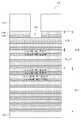
도 1a 내지 도 1f는 본 발명의 일 실시예에 따른 반도체 소자를 제조하는 방법을 설명하기 위한 단면도들이다. 도 2 및 도 3은 본 발명의 일 실시예에 따른 반도체 소자를 제조하는 방법을 설명하기 위한 순서도들이다.1A to 1F are cross-sectional views illustrating a method of manufacturing a semiconductor device according to an embodiment of the present invention. 2 and 3 are flowcharts for explaining a method of manufacturing a semiconductor device according to an embodiment of the present invention.
도 1a를 참조하면, 기판(100) 상에 복수의 제1 물질막들(110) 및 복수의 제2 물질막들(120)을 교번적으로 적층하여 스택 구조물(STK)을 형성할 수 있다.Referring to FIG. 1A, a plurality of
상기 제1 물질막들(110)은 n개가 적층되고, 상기 제2 물질막들(120)은 m개가 적층될 수 있다. 상기 제1 물질막들(110) 각각은 동일한 제1 두께를 가지며, 상기 제2 물질막들(120) 각각은 동일한 제2 두께를 가질 수 있다.N pieces of the
본 발명의 일 실시예에 따르면, 상기 제1 물질막(110)은 제1 에천트에 의해 식각되고, 상기 제2 물질막(120)은 제2 에천트에 의해 식각될 수 있다. 또한, 상기 제1 물질막(110)은 상기 제2 에천트에 의해 실질적으로 식각되지 않으며, 상기 제2 물질막(120)은 상기 제1 에천트에 의해 실질적으로 식각되지 않을 수 있다. 상기 제1 및 제2 에천트들 각각은 제1 및 제2 물질막들(110, 120)을 실질적으로 식각하는 식각 가스와 캐리어 가스를 포함할 수 있다.According to an embodiment of the present invention, the
일 측면에 따르면, 상기 제1 물질막(110)이 실리콘 산화막과 같은 산화막을 포함하면, 상기 제1 에천트는 CxFy계열의 식각 가스를 포함할 수 있다. 상기 제2 물질막(120)은 실리콘 질화막과 같은 질화막을 포함하면, 상기 제2 에천트는 CxHyFz계열의 식각 가스를 포함할 수 있다.According to an aspect, when the
상기 스택 구조물(STK)은 상부 및 하부를 포함할 수 있다. 일 실시예에 따르면, 상기 스택 구조물(STK)의 하부는 첫 번째 제1 물질막(110)부터 n-k번째 제1 물질막(110)까지, 및 첫 번째 제2 물질막(120)부터 m-k번째 제2 물질막(120)까지를 포함할 수 있다. 상기 스택 구조물(STK)의 상부는 n-k+1번째 제1 물질막(110)부터 n번째 제1 물질막(110)까지, 및 m-k+1번째 제2 물질막(120)부터 m번째 제2 물질막(120)까지를 포함할 수 있다. 이때, n>k>1이며, n 및 k는 양의 정수이다. 상기 스택 구조물(STK)의 상부 및 하부들 구간은 식각 공정에 따라 변경될 수 있다.The stack structure STK may include upper and lower portions. The lower portion of the stack structure STK may extend from the
도 1b를 참조하면, 상기 스택 구조물(STK) 상에 마스크 패턴(130)을 형성할 수 있다. 상기 마스크 패턴(130)은 식각될 부분의 스택 구조물(STK)의 상부면을 노출시킬 수 있다.Referring to FIG. 1B, a
상기 마스크 패턴(130)은 상기 제1 및 제2 에천트들에 의해 실질적으로 식각되지 않은 물질을 포함할 수 있다. 일 예로, 상기 마스크 패턴(130)은 레지스트를 포함할 수 있다.The
도 1c 및 도 2를 참조하면, 상기 마스크 패턴(130)을 식각 마스크로 사용하여, 상기 제1 에천트를 이용하여 n번째 제1 물질막(110)을 식각하여 n번째 제1 패턴(110P)을 형성할 수 있다.(단계 S100) 일 측면에 따르면, 상기 제1 물질막(110)이 실리콘 산화막을 포함하고, 상기 제1 에천트가 CxFy를 포함하는 경우, 상기 제1 물질막(110)의 식각으로 발생되는 제1 식각 반응 가스는 CxOy를 포함할 수 있다.1C and 2, the n-th
본 발명의 일 실시예에 따르면, 상기 제1 물질막(110)의 식각은 제1 식각 종말점을 검출하여 중지될 수 있다.(단계 S110) 상기 제1 식각 종말점을 검출하는 방법은 분광법(optical emission spectroscopy) 방식, 간섭현상을 이용하는 방식, RF 발생기 시스템에서 발생하는 RF파의 전압과 전류를 검출하는 방식을 포함할 수 있다.According to an embodiment of the present invention, the etching of the
본 실시예에서 상기 분광법 방식으로 상기 제1 식각 종말점(first end point: first EDP)을 검출하는 것을 예시적으로 설명하기로 한다. 그러나, 본 발명이 이로 한정되는 것을 아니다. 상기 제1 물질막(110)은 상기 제1 에천트에 의해 식각되고, 그 반응 산물로 제1 식각 반응 가스를 배출할 수 있다. 상기 분광법을 이용하는 식각 종말점 검출 방법은 상기 제1 식각 반응 가스의 제1 EPD 신호를 시간에 따라 검출하며, 시간에 따라 변하는 상기 제1 EPD 신호를 이용하는 방법이다. 상기 제1 EPD 신호는 제1 시작점에서 점진적으로 증가하다가 제1 최고점(peak)에 도달하고 점진적으로 감소할 수 있다. 예컨대, 상기 제1 식각 종말점은, 상기 제1 최고점을 지난 후, 상기 제1 최고점의 90%에 해당되는 지점일 수 있다. 이 지점에서 상기 제1 에천트의 주입을 중지하고 m번째 제2 물질막(120)의 식각을 위한 제2 에천트의 주입을 준비할 수 있다.In this embodiment, the detection of the first end point (first EDP) by the spectroscopic method will be described as an example. However, the present invention is not limited thereto. The
이때, 상기 제1 EPD 신호에서 상기 제1 시작점과 상기 제1 최고점의 사이의 차이를 제1 신호값이라 한다. 상기 스택 구조물의 제1 물질막들(110)을 각각 식각하면 할수록 상기 제1 신호값들은 점차 감소할 수 있다.Here, a difference between the first starting point and the first peak in the first EPD signal is referred to as a first signal value. As the first material layers 110 of the stack structure are etched, the first signal values may gradually decrease.
상기 n번째 제1 물질막(110)의 식각 공정으로 상기 m번째 제2 물질막(120)의 상부면을 부분적으로 노출시키는 개구(140)를 형성할 수 있다. 상기 개구(140)는 상기 스택 구조물(STK)의 식각 공정을 진행할수록 깊어질 수 있다. 일 측면에 따르면, 상기 개구(140)에 의해 노출되는 상기 n번째 제1 패턴(110P)의 측면은, 상기 개구(140)에서 상기 n번째 제1 패턴(110P) 쪽으로 오목한 곡면을 가질 수 있다.The
본 발명의 일 실시예에 따르면, 상기 n번째 제1 물질막(110)을 식각하기 위한 상기 제1 에천트의 주입 레서피(recipe)가 저장될 수 있다.(단계 S130) 상기 제1 에천트의 레서피는 예를 들면, 제1 에천트의 주입 시간, 제1 에천트의 주입 양 및 상기 제1 에천트 내 식각 가스와 캐리어 가스 사이의 비율 등을 포함할 수 있다. 상기 스택 구조물(STK)의 제1 물질막들(110) 각각을 식각하기 위한 제1 에천트의 레서피는 지속적으로 저장되며, 상기 개구(140)의 깊이에 대한 제1 에천트의 레서피의 경향성(trend)을 획득할 수 있다. 예를 들면, 상기 스택 구조물의 제1 물질막들(110)을 식각할수록 상기 제1 에천트의 주입 시간은 점차 증가하는 경향성을 가질 수 있다. 나아가, 상기 개구(140)의 깊이에 대한 제1 에천트의 주입 시간 함수를 획득할 수 있다.According to an embodiment of the present invention, an injection recipe of the first etchant for etching the nth
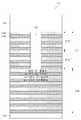
도 1d를 참조하면, 상기 마스크 패턴(130)을 식각 마스크로 사용하여, 상기 제2 에천트를 이용하여(단계 S140) 상기 m번째 제2 물질막(120)을 식각하여, m번째 제2 패턴(120P)을 형성할 수 있다. 일 측면에 따르면, 상기 제2 물질막(120)이 실리콘 질화막을 포함하고, 상기 제2 에천트가 CxHyFz를 포함하는 경우, 상기 제2 물질막(120)의 식각으로 발생되는 제2 식각 반응 가스는 CxNy를 포함할 수 있다.Referring toFIG. 1D , the m-th
본 발명의 일 실시예에 따르면, 상기 제2 물질막(120)의 식각은 제2 식각 종말점을 검출하여 중지될 수 있다.(단계 S150) 상기 제2 물질막(120)은 상기 제2 에천트에 의해 식각되고, 그 반응 산물로 제2 식각 반응 가스를 배출할 수 있다. 상기 제2 식각 반응 가스의 제2 EPD 신호를 시간에 따라 검출하며, 시간에 따라 변하는 상기 제2 EPD 신호를 이용하여 제2 식각 종말점을 검출할 수 있다. 상기 제2 식각 반응 가스의 신호는 제2 시작점에서 점진적으로 증가하다가 제2 최고점에 도달하고 점진적으로 감소할 수 있다. 예컨대, 상기 제2 식각 종말점은 상기 제2 최고점이 지난 후 상기 제2 최고점의 90%에 해당되는 지점일 수 있다. 이 지점에서 상기 제2 에천트의 주입을 중지하고, n-1번째 제1 물질막(110)의 식각을 위한 제1 에천트의 주입을 준비할 수 있다.According to an embodiment of the present invention, the etching of the
이때, 상기 제2 EPD 신호에서 상기 제2 시작점과 상기 제2 최고점 사이의 차이를 제2 신호값이라 한다. 상기 스택 구조물의 제2 물질막들(120)을 각각 식각하면 할수록 상기 제2 신호값들은 점차 감소할 수 있다.In this case, a difference between the second starting point and the second peak in the second EPD signal is referred to as a second signal value. As the second material layers 120 of the stack structure are etched, the second signal values may gradually decrease.
상기 m번째 제2 물질막(120)의 식각 공정으로 상기 개구(140)를 더 깊어지고, 상기 개구(140)는 n-1번째 제1 물질막(110)의 상부면을 부분적으로 노출시킬 수 있다. 일 측면에 따르면, 상기 개구(140)에 의해 노출된 상기 m번째 제2 패턴(120P)의 측면은, 상기 개구(140)에서 상기 m번째 제2 패턴(120P) 쪽으로 오목한 곡면을 가질 수 있다.The
본 발명의 일 실시예에 따르면, 상기 m번째 제2 물질막(120)을 식각하기 위한 상기 제2 에천트의 주입 레서피가 저장될 수 있다.(단계 S160) 상기 제2 에천트의 레서피는 예를 들면, 제2 에천트의 주입 시간, 제2 에천트의 주입 양 및 제2 에천트 내 식각 가스와 캐리어 가스 사이의 비율 등을 포함할 수 있다. 상기 스택 구조물(STK)의 제2 물질막들(120) 각각을 식각하기 위한 제2 에천트의 레서피는 지속적으로 저장되며, 상기 개구(140)의 깊이에 따른 제2 에천트의 레서피의 경향성을 획득할 수 있다. 예를 들면, 스택 구조물의 제2 물질막들(120)을 식각할수록 상기 제2 에천트의 주입 시간은 점차 증가하는 경향성을 가질 수 있다. 나아가, 상기 개구(140)의 깊이에 대한 제2 에천트의 주입 시간 함수를 획득할 수 있다.According to an embodiment of the present invention, the injection recipe of the second etchant for etching the mth
도 1c 및 도 1d에서 설명된 공정을 반복적으로 수행하여, 상기 스택 구조물(STK)의 제1 및 제2 물질막들(110, 120)을 적층된 순서와 반대로 즉, 상기 마스크 패턴(140)에 인접한 순서대로 식각하여 제1 패턴들(110P) 및 제2 패턴들(120P)을 형성할 수 있다.1C and 1D, the first and
그러나, 상기 스택 구조물(STK) 내 제1 및 제2 물질막들(110, 120)을 모두 식각하기 용이하지 않다. 특히, 스택 구조물(STK)의 하부의 제1 및 제2 물질막들(110, 120)을 식각하기 힘들다. 이하에서 상세하게 설명하기로 한다.However, it is not easy to etch both the first and
도 4는 시간에 따른 제1 및 제2 식각 반응 가스들의 제1 및 제2 EPD 신호들의 신호를 도시한 그래프이다. 도 4를 참조하면, 시간에 따라 상기 제1 및 제2 신호값들이 지속적으로 감소할 수 있다. 이는, 식각 공정이 지속할수록 상기 스택 구조물(STK)에 형성되는 개구(140)의 깊이가 깊어지고, 상기 제1 및 제2 에천트들은 상기 개구(140)를 통해 주입되고, 상기 제1 및 제2 식각 반응 가스들은 상기 개구(140)를 통해 배출되는데, 상기 개구(140)의 깊이가 깊어질수록 상기 제1 및 제2 에천트들과 제1 및 제2 식각 반응 가스들의 출입이 용이하지 않기 때문일 수 있다.4 is a graph showing the signals of the first and second EPD signals of the first and second etching reaction gases with time. Referring to FIG. 4, the first and second signal values may continuously decrease with time. This is because as the etching process continues, the depth of the
전술한 바와 같이 상기 제1 및 제2 신호값들이 감소하여 0인 경우, 도 1c 및 도 1d에서 설명된 공정으로 제1 및 제2 물질막들(110, 120)을 식각할 수 없다. 일 측면에 따르면, 상기 제1 및 제2 신호값들 각각이 0이 되기 전부터 도 1c 및 도 1d에서 설명된 공정으로 제1 및 제2 물질막들(110, 120)을 식각하기 용이하지 않을 수 있다. 따라서, 0보다 큰 제1 기준값을 정하여 상기 제1 기준값보다 작은 시점부터 다른 방법(도 1f 및 도 2 참조)으로 제1 및 제2 물질막들(110, 120)을 식각해야 한다. 상기 제1 기준값은 목적하는 공정 마다 완성되는 반도체 소자에 따라 상이할 수 있다.As described above, when the first and second signal values decrease to 0, the first and
본 발명의 일 실시예에 따르면, 상기 제1 및 제2 신호값들 각각을 매 단계 확인하여, 상기 제1 및 제2 신호값들을 상기 제1 기준값과 비교하여(단계 S160), 도 1c 및 도 1d에서 설명된 공정으로 제1 및 제2 물질막들(110, 120)을 식각할지 결정할 수 있다.According to an embodiment of the present invention, the first and second signal values are checked at each step, and the first and second signal values are compared with the first reference value (step S160) It is possible to determine whether to etch the first and
일 측면 따르면, 상기 제1 및 제2 신호값들 중 적어도 하나가 제1 기준값보다 큰 경우, 도 1c 및 도 1d에서 설명된 제1 공정으로 제1 및 제2 물질막들을 식각할 수 있다.(단계 S100, 단계 S140) 즉, 상기 제1 공정으로 스택 구조물(STK)의 상부를 식각할 수 있다. 나아가, 상기 제1 및 제2 신호값들 중 적어도 하나가 제1 기준값보다 작은 시점이 상기 제1 공정이 종료하는 시점일 수 있다.According to an aspect, if at least one of the first and second signal values is greater than a first reference value, the first and second material layers may be etched by the first process described in Figures 1C and 1D. Steps S100 and S140). That is, the upper portion of the stack structure (STK) may be etched in the first step. Further, a time point at which at least one of the first and second signal values is less than a first reference value may be a time point at which the first process ends.
상기 제1 및 제2 신호값들 각각이 상기 제1 기준값보다 작은 경우에는(단계 S120, 단계 S160, 단계 S200), 도 1f 및 도 2에 도시된 바와 같이 스택 구조물(STK)의 하부는 상기 스택 구조물(STK)의 상부와는 상이한 제2 공정으로 식각될 수 있다. 상기 제2 공정은 도 2에서 A 공정에 대응될 수 있다.If the first and second signal values are smaller than the first reference value (step S120, step S160, step S200), the lower part of the stack structure STK as shown in FIG. 1F and FIG. 2, Can be etched into a second process different from the top of the structure (STK). The second process may correspond to the process A in Fig.
이하, 상기 스택 구조물(STK)의 하부를 식각하는 공정(A 공정)을 보다 상세하게 설명하기로 한다.Hereinafter, the process of etching the bottom of the stack structure (STK) (A process) will be described in more detail.
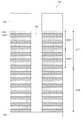
전술한 바와 같이 상기 스택 구조물(STK)의 상부를 식각하는 동안 상기 제1 및 제2 에천트들 각각의 레서피들을 매번 저장하여(단계 S130, 단계 S170), 상기 제1 및 제2 에천트들의 레서피들의 경향성을 획득할 수 있다. 일 예로, 상기 개구(140)의 깊이에 대한 상기 제1 및 제2 에천트들의 주입 시간 함수를 획득할 수 있다. 다른 예로, 상기 개구(140)의 깊이에 대한 상기 제1 및 제2 에천트들의 주입 양 함수를 획득할 수 있다. 또 다른 예로, 상기 개구(140)의 깊이에 대한 상기 제1 및 제2 에천트들 내 식각 가스의 비율을 획득할 수 있다.As described above, during the etching of the upper part of the stack structure (STK), the recipes of the first and second etchants are stored each time (step S130, step S170), and the recipe of the first and second etchants Can be obtained. As an example, the injection time function of the first and second etchants with respect to the depth of the
상기 스택 구조물(STK)의 하부는 상기 개구(140)의 깊이에 대한 상기 제1 및 제2 에천트들의 주입 시간 함수를 기반으로 제1 및 제2 에천트들을 변경하여, 상기 스택 구조물(STK) 하부의 제1 및 제2 물질막들(110, 120)을 각각 식각할 수 있다.The lower portion of the stack structure (STK) changes the first and second etchants based on the injection time function of the first and second etchants with respect to the depth of the opening (140) The first and
도 1f 및 3을 참조하면, 상기 제1 신호값이 상기 제1 기준값보다 작으면(단계 S200), 상기 스택 구조물(STK) 상부를 식각하는 동안 획득된 함수들을 이용하여 상기 제1 에천트를 주입하여 n-k번째 제1 물질막(110)을 식각할 수 있다.(단계 S210) 상기 함수들에 따라 제1 에천트 주입을 중지하여(단계 S220) n-k번째 제1 물질 패턴(110P)을 형성할 수 있다. 상기 함수들을 이용하여 제2 에천트를 주입하여 m-k번째 제2 물질막(120)을 식각할 수 있다. (단계 S230) 상기 함수들에 따라 상기 제2 에천트 주입을 중지하여(단계 S240) m-k번째 제2 물질 패턴(120P)을 형성할 수 있다. 에천트를 주입할 준비를 수행할 수 있다. 도 3의 공정은 첫 번째 제1 물질막(110) 또는 첫 번째 제2 물질막(120)까지(단계 S250) 반복적으로 수행될 수 있다.Referring to FIGS. 1F and 3, if the first signal value is smaller than the first reference value (step S200), the first etchant is injected using the functions obtained during the etching of the upper part of the stack structure STK The nk-th
도 1b 내지 도 1f, 도 2 및 도 3에서 설명된 상기 식각 공정으로 상기 스택 구조물(STK)은, 서로 교번적으로 적층된 제1 패턴들(110P) 및 상기 제2 패턴들(120P)과, 상기 스택 구조물(STK)을 관통하는 개구(140)를 포함할 수 있다. 상기 개구(140)에 의해 노출된 상기 스택 구조물(STK)의 내측면은 엠보싱(embossing) 구조를 가질 수 있다.The stack structure (STK) may be formed by stacking
하기에서 설명되는 공정은 상기 스택 구조물의 상부를 식각하는 동안 선택적으로 추가될 수 있다. 이하의 공정을 편의 상 가스 램핑(gas ramping) 공정이라 한다.The process described below can be selectively added while etching the top of the stack structure. The following process is referred to as a gas ramping process for convenience.
도 5는 본 발명의 다른 실시예에 따른 반도체 소자의 제조 방법을 설명하기 위한 순서도이다. 도 5에 도시된 공정을 도 2 및 도 3에서 설명된 공정에 추가하거나, 생략할 수 있다.5 is a flowchart illustrating a method of manufacturing a semiconductor device according to another embodiment of the present invention. The process shown in Fig. 5 may be added to the process described in Figs. 2 and 3, or may be omitted.
도 4에서, 상기 스택 구조물(STK)의 상부의 하단부 구간은, 상기 상부의 상단부 구간보다 제1 및 2 최고점들이 낮아지고, 인접한 제1 및 제2 최고점들 사이 폭이 넓어지는 것을 알 수 있다. 상기 제1 및 2 최고점들이 낮아지는 것은 개구(140, 도 1d 참조)가 깊어짐에 따라 제1 및 제2 식각 반응 가스들의 검출되는 양이 적어지는 것을 의미하며, 상기 제1 및 제2 최고점들 사이 폭이 넓어지는 것은 상기 제1 및 제2 식각 반응 가스들이 검출되는 시간이 증가하는 것을 의미할 수 있다. 상기 제1 및 제2 식각 반응 가스들의 검출되는 양이 감소하고 검출되는 시간이 증가한다는 것은 상기 제1 및 제2 에천트들이 상기 제1 및 제2 물질막들(110, 120)까지 도달하는 거리가 증가하고, 그 거리를 이동하는 동안 제1 및 제2 에천트들은 이미 식각된 제1 및 제2 패턴들(110P, 120P)에서 소모되거나, 이동하는 동안 소멸될 수 있다.In FIG. 4, it can be seen that the first and second highest peaks of the upper part of the upper part of the stack structure STK are lower than the upper part of the upper part of the upper part of the stack structure STK, and the width between adjacent first and second peaks is widened. The lowering of the first and second highest peaks means that the detected amount of the first and second etch reactants is decreased as the opening 140 (see FIG. 1D) is deepened, and between the first and second highest peaks The widening of the width may mean that the time for detecting the first and second etching reactive gases is increased. The decrease in the detected amount of the first and second etching reactive gases and the increase in the detected time means that the distance between the first and second etchants reaching the first and
상기의 구간에서는, 상기 제1 및 제2 신호값들이 상기 제1 기준값보다는 크지만 제1 및 제2 물질막들(110, 120)을 식각하는 공정이 시간이 길어질 수 있다. 따라서, 상기 구간의 제1 및 제2 물질막들(110, 120)을 효율적으로 식각하기 위하여, 도 5에 도시된 가스 램핑 공정을 이용할 수 있다.In the above section, although the first and second signal values are larger than the first reference value, the process of etching the first and
도 6은 가스 램핑 공정을 설명하기 위한 그래프이다. 도 6을 참조하면, 개구가 깊어질수록(공정의 시간이 증가할수록) 상기 주입되는 제1 에천트 및 제2 에천트의 양이 단계적으로 증가될 수 있다. 이는 가스 램핑의 일 예이며, 제1 및 제2 에천트들의 주입 시간을 단계적으로 증가시키거나, 제1 및 제2 에천트들 각각 내의 캐리어 가스에 대한 식각 가스의 양을 단계적으로 증가시킬 수 있다.6 is a graph for explaining the gas ramping process. Referring to FIG. 6, the amount of the first etchant and the second etchant to be injected may be increased step by step as the opening is deeper (the time of the process is increased). This is an example of gas ramping and may increase the injection time of the first and second etchants step by step or increase the amount of etch gas for the carrier gas in each of the first and second etchants .
도 1d 및 도 5에 도시된 n-d번째 제1 물질막(110) 및 n-d-1번째 제1 물질막(110)을 식각하는 것을 예시적으로 설명한다. n-d번째 제1 물질막(110)을 제1 에천트로 식각하는 동안, 제1 식각 종말점이 검출되고, 제1 신호값이 상기 제1 기준값보다 큰 경우, 상기 제1 신호값을 제2 기준값과 비교하는 단계(단계 S300)를 더 수행할 수 있다. 이때, 상기 제2 기준값은 상기 제1 기준값보다는 크다.The etching of the n-d-th
상기 제1 신호값이 상기 제2 기준값보다 크다면, n-d-1번째 제1 물질막(110)은 n-d번째 제1 물질막을 식각할 때 사용한 제1 에천트의 레서피를 이용하여 상기 제1 에천트를 주입할 수 있다. 도 1c에서 설명한 공정과 실질적으로 동일할 수 있다. (단계 S400~단계 S420)If the first signal value is larger than the second reference value, the nd-1 th
상기 제1 신호값이 상기 제2 기준값보다 작다면, n-d-1번째 제1 물질막(110)부터 가스 램핑 동작(단계 S310)이 추가될 수 있다. 일 예로, n-d-1번째 제1 물질막(110)은 상기 n-d번째 제1 물질막(110)을 식각하는 제1 에천트의 레서피와 상이한 레서피로 식각될 수 있다.(단계 S310, 단계 S320) 예를 들면, 상기 n-d-1번째 제1 물질막(110)의 제1 에천트가 n-d번째 제1 물질막(110)의 제1 에천트보다 그 양이 많거나, 그 주입 시간이 길거나, 그 내 캐리어 가스에 대한 식각 가스의 비율이 많을 수 있다. 상기 n-d-1번째 제1 물질막(110)의 식각은 제1 EPD 신호에 의한 제1 식각 종말점 검출(단계 S330) 후 중지될 수 있다. 상기 제1 에천트의 레서피는 저장될 수 있다.If the first signal value is smaller than the second reference value, a gas ramping operation (step S310) may be added from the (n-d-1) th
상기 가스 램핑 공정이 수행되는 시점 즉, n-d-1번째 제1 물질막부터 n-k번째 제1 물질막까지 매 단계 변경된 레서피에 따라 제1 에천트가 주입될 수 있다. 예를 들면, 상기 제1 에천트의 양은 단계적으로 증가하고, 주입 시간은 단계적으로 증가하고, 캐리어 가스에 대한 식각 가스의 비율이 증가할 수 있다. 상기 n-d-1번째 제1 물질막부터 n-k+1번째 제1 물질막까지 주입되는 제1 에천트들의 레서피들은 각각 저장되며, 상기 개구의 깊이에 따른 제1 에천트의 레서피 경향성을 획득할 수 있다. 나아가, 상기 개구(140)의 깊이에 대한 제1 에천트의 레서피 함수를 획득할 수 있다.The first etchant may be injected at a time when the gas ramping process is performed, that is, according to a recipe that is changed every step from the (n-d) -th first material film to the (n-k) th first material film. For example, the amount of the first etchant may increase stepwise, the injection time may increase stepwise, and the ratio of etch gas to carrier gas may increase. Recipes of the first etchants injected from the first nd-1 th material layer to the n-k + 1 th first material layer are respectively stored, and the recipe tendency of the first etchant is obtained according to the depth of the opening . Further, a recipe function of the first etchant with respect to the depth of the
상기의 공정을 반복하면, 상기 제1 신호값이 제1 기준값보다 작다면,(단계 S340) 상기 가스 램핑 공정을 종료하고 도 3에서 설명된 스택 구조물(STK)의 하부의 식각 공정이 시작될 수 있다. 상기 스택 구조물(STK)의 하부의 식각은 상기 제1 및 제2 에천트들의 레서피 함수를 기반으로 제1 및 제2 에천트들을 변경하여 제1 및 제2 물질막들(110, 120)을 식각할 수 있다.If the first signal value is smaller than the first reference value (step S340), the gas ramping process is terminated and the etching process of the lower part of the stack structure STK described in FIG. 3 may be started . Etching of the lower portion of the stack structure STK changes the first and second etchants based on the recipe function of the first and second etchants to etch the first and
도 7a 내지 도 7j는 본 발명의 일 실시예에 따른 반도체 소자를 제조하는 방법을 설명하기 위한 단면도들이다. 본 실시예의 반도체 소자는 전하 트랩형 플래시 메모리 소자를 예시적으로 설명하기로 하지만 본 발명이 이로 한정되지는 않는다.7A to 7J are cross-sectional views illustrating a method of manufacturing a semiconductor device according to an embodiment of the present invention. Although the semiconductor device of this embodiment is illustratively described as a charge trap type flash memory device, the present invention is not limited thereto.
도 7a를 참조하면, 기판(200) 상에 복수의 절연막들(210) 및 복수의 희생막들(220)이 교번된 스택 구조물(STK)을 형성할 수 있다.Referring to FIG. 7A, a stack structure STK in which a plurality of insulating
상기 절연막들(210) 각각은 실리콘 산화물을 포함하고, 상기 희생막들(220) 각각은 실리콘 질화물을 포함할 수 있다.Each of the insulating
도 7b를 참조하면, 상기 스택 구조물(STK)의 절연막들(210) 및 희생막들(220)을 식각하여, 상기 스택 구조물(STK)을 관통하는 관통 홀(230)이 형성될 수 있다. 상기 콘택 홀은 기판을 노출시킬 수 있다.Referring to FIG. 7B, the insulating
상기 식각 공정은 도 1a 내지 도 1f, 도 2 내지 도 4에서 설명된 공정을 이용하여 수행될 수 있다. 본 실시예에서 상기 절연막들(210) 및 상기 희생막들(220) 각각은 도 1a 내지 도 1f의 제1 물질막들(110) 및 제2 물질막들(120)에 각각 대응될 수 있다.The etching process may be performed using the process described in Figs. 1A to 1F, 2 to 4. In this embodiment, each of the insulating
도 7b에 도시된 바와 같이, 상기 관통 홀(230)에 의해 노출된 절연막들(210) 및 희생막들(220) 각각의 측면은 오목한 곡면을 가질 수 있다.As shown in FIG. 7B, the side surfaces of each of the insulating
도 7c를 참조하면, 상기 관통 홀(230) 측면을 따라 터널 절연막(232) 및 전하 저장막(234)을 형성할 수 있다. 상기 터널 절연막(232) 및 상기 전하 저장막(234)은 상기 관통 홀(230)을 매립하지 않을 수 있다.Referring to FIG. 7C, a
상기 터널 절연막(232)은 상기 전하 저장막(234)보다 큰 밴드 갭을 갖는 물질 중 하나일 수 있다. 예를 들어, 상기 터널 절연막(232)은 알루미늄 산화막 및 하프늄 산화막 등과 같은 고유전막들 중의 하나일 수 있다. 상기 전하 저장막은(234) 실리콘 질화막과 같은 트랩 사이트가 풍부한 절연막, 부유 게이트 전극, 또는 도전성 나노 닷들(conductive nano dots)을 포함하는 절연막 중의 하나일 수 있다.The
도 7d를 참조하면, 상기 관통 홀(230)을 도전물로 채워 수직 액티브 패턴(240) 및 도전 패드(242)를 형성할 수 있다.Referring to FIG. 7D, the vertical
일 측면에 따르면, 상기 수직 액티브 패턴(240)을 형성하는 것은, 상기 콘택 홀(230)의 측면을 따라 연장되어 상기 기판과 연결되는 반도체 패턴(235)을 형성한 후, 상기 반도체 패턴(235) 내부를 채우는 절연막(237)을 형성하는 것을 포함할 수 있다. 상기 반도체 패턴(235)은 실리콘(Si), 게르마늄(Ge) 또는 이들의 혼합물을 포함할 수 있으며, 불순물이 도핑된 반도체이거나 불순물이 도핑되지 않은 상태의 진성 반도체(intrinsic semiconductor)일 수도 있다. 또한, 단결정, 비정질(amorphous), 및 다결정(polycrystalline) 중에서 선택된 적어도 어느 하나를 포함하는 결정 구조를 가질 수 있다. 한편, 상기 수직 액티브 패턴(240)은 속이 빈 파이프 형태(pipe-shaped) 또는 마카로니 형태(macaroni-shaped)일 수 있다. 이때, 상기 수직 액티브 패턴(240)의 하단은 닫힌 상태(closed state)일 수 있다.Forming the vertical
상기 도전 패드(242)는 상기 수직 액티브 패턴(240)의 상단에 형성될 수 있다. 상기 도전 패드(242)는 불순물이 도핑된 불순물 영역이거나, 도전 물질로 이루어질 수 있다. 상기 수직 액티브 패턴(240), 상기 도전 패드(242) 및 상기 스택 구조물(STK)의 상부면을 덮는 캡핑 유전막(244)을 형성할 수 있다.The
도 7e를 참조하면, 상기 절연 패턴들(210P) 및 상기 희생 패턴들(220P)이 형성된 스택 구조물(STK)을 식각하여, 일 방향으로 연장하는 트렌치(250)를 형성할 수 있다. 상기 식각 공정에 의해 상기 트렌치(250)를 형성함과 동시에, 상기 수직 액티브 패턴(240)을 따라 다수의 절연 패턴들(210P) 및 희생 패턴들(220P)이 번갈아 배치될 수 있다.Referring to FIG. 7E, the stack structure STK having the insulating
상기 식각 공정은 도 1a 내지 도 1f, 도 2 내지 도 4에서 설명된 공정을 이용하여 수행될 수 있다. 본 실시예에서 상기 절연 패턴들(210P) 및 상기 희생 패턴들(220P) 각각은 도 1a 내지 도 1f의 제1 패턴들 및 제2 패턴들에 각각 대응될 수 있다.The etching process may be performed using the process described in Figs. 1A to 1F, 2 to 4. In this embodiment, each of the insulating
도 7e에 도시된 바와 같이, 상기 트렌치(250)에 의해 노출된 상기 절연 패턴들(210P) 및 상기 희생 패턴들(220P) 각각의 측면은 오목한 곡면을 가질 수 있다.7E, the sides of each of the
도 7f를 참조하면, 상기 트렌치(250)에 의해 노출된 희생 패턴들(220P)을 제거하여, 상기 절연 패턴들(210P) 사이에 리세스들(252)을 형성할 수 있다.Referring to FIG. 7F, the
도 7g를 참조하면, 상기 리세스들(252)에 블로킹 절연막(254)을 컨포멀하게 형성할 수 있다. 상기 블로킹 절연막(254)은 터널 절연막(232)보다 작고 전하 저장막(234)보다 큰 밴드 갭을 갖는 물질들 중의 한가지일 수 있다. 예를 들어, 블록킹 절연막(254)은 알루미늄 산화막 및 하프늄 산화막 등과 같은 고유전막들 중의 하나일 수 있다.Referring to FIG. 7G, a blocking insulating
도 7h를 참조하면, 상기 블로킹 절연막(254)이 형성된 리세스들 각각을 채우는 게이트 패턴(255)을 형성할 수 있다. 상기 게이트 패턴(255)은 베리어 금속막(도시되지 않음) 및 금속막(도시되지 않음)이 차례로 적층된 구조일 수 있다. 상기 베리어 금속막은 예를 들어, TiN, TaN 또는 WN와 같은 금속 질화막으로 이루어질 수 있다. 그리고, 상기 금속막은 예를 들어, W, Al, Ti, Ta, Co 또는 Cu와 같은 금속 물질들로 이루어질 수 있다.Referring to FIG. 7H, a
일 측면에 따르면, 상기 게이트 패턴(255)을 형성하는 것은, 상기 트렌치(250)를 부분적으로 또는 완전하게 채우는 베리어막 및 도전막을 순차적으로 형성한 후, 상기 트렌치(250) 내에 잔류하는 베리어막 및 도전막을 식각하여, 게이트 패턴(255)을 형성할 수 있다. 이에 엠보싱 형상을 갖는 스택 구조물(STK)의 측면은 상기 식각 공정을 통해 수직인 면을 가질 수 있다.According to an aspect of the present invention, forming the
도 7i를 참조하면, 상기 트렌치(250)에 의해 노출된 기판(200)에 공통 소스 영역(257)을 형성할 수 있다. 상기 공통 소스 영역(257)은 상기 기판(200)에 도핑된 불순물과 다른 타입의 불순물이 도핑된 영역일 수 있다.Referring to FIG. 7I, a
이어서, 상기 트렌치(250) 측면에 컨포멀하게 스페이서(259)를 형성한 후, 상기 스페이서(259)가 형성된 트렌치(250)를 매립하며, 상기 공통 소스 영역(257)과 전기적으로 연결되는 공통 소스 라인(260)을 형성할 수 있다. 상기 공통 소스 라인(260)은 금속(ex, 텅스텐, 구리 또는 알루미늄 등), 도전성 금속질화물(ex, 질화티타늄 또는 질화탄탈늄 등) 및 전이 금속(ex, 티타늄 또는 탄탈늄 등) 등에서 선택된 적어도 하나를 포함할 수 있다.A
도 7j를 참조하면, 상기 공통 소스 라인(260) 및 상기 수직 액티브 패턴(240)의 상부면을 덮는 층간 절연막(262)을 형성할 수 있다. 상기 층간 절연막(262)을 관통하여, 상기 수직 액티브 패턴(240)에 접촉하는 비트 라인 플러그(264)와 상기 비트 라인 플러그(264)와 전기적으로 연결되는 비트 라인(BL)을 형성할 수 있다.Referring to FIG. 7J, an
상기 비트 라인 플러그(264) 및 비트 라인(BL)은 금속(ex, 텅스텐, 구리 또는 알루미늄 등), 도전성 금속질화물(ex, 질화티타늄 또는 질화탄탈늄 등) 및 전이 금속(ex, 티타늄 또는 탄탈늄 등) 등에서 선택된 적어도 하나를 포함할 수 있다.The
도 8은 본 발명의 실시예들에 따라 형성된 반도체 소자를 포함하는 전자 시스템의 일 예를 간략히 도시한 블록도이다.8 is a block diagram briefly illustrating an example of an electronic system including a semiconductor device formed in accordance with embodiments of the present invention.
도 8을 참조하면, 본 발명의 일 실시 예에 따른 전자 시스템(1100)은 컨트롤러(1110), 입출력 장치(1120, I/O), 기억 장치(1130, memory device), 인터페이스(1140) 및 버스(1150, bus)를 포함할 수 있다. 상기 컨트롤러(1110), 입출력 장치(1120), 기억 장치(1130) 및/또는 인터페이스(1140)는 버스(1150)를 통하여 서로 결합 될 수 있다. 버스(1150)는 데이터들이 이동되는 통로(path)에 해당한다. 컨트롤러(1110), 입출력 장치(1120, I/O), 기억 장치(1130, memory device), 및/또는 인터페이스(1140)은 본 발명의 실시예들에 따라 제조된 반도체 소자를 포함할 수 있다.8, an
컨트롤러(1110)는 마이크로프로세서, 디지털 신호 프로세스, 마이크로컨트롤러, 및 이들과 유사한 기능을 수행할 수 있는 논리 소자들 중에서 적어도 하나를 포함할 수 있다. 입출력 장치(1120)는 키패드(keypad), 키보드 및 디스플레이 장치등을 포함할 수 있다. 기억 장치(1130)는 데이터 및/또는 명령어 등을 저장할 수 있다. 인터페이스(1140)는 통신 네트워크로 데이터를 전송하거나 통신 네트워크로부터 데이터를 수신하는 기능을 수행할 수 있다. 인터페이스(1140)는 유선 또는 무선 형태일 수 있다. 예컨대, 인터페이스(1140)는 안테나 또는 유무선 트랜시버 등을 포함할 수 있다. 도시하지 않았지만, 전자 시스템(1100)은 컨트롤러(1110)의 동작을 향상시키기 위한 동작 기억 소자로서, 고속의 디램 소자 및/또는 에스램 소자 등을 더 포함할 수도 있다.The
전자 시스템(1100)은 개인 휴대용 정보 단말기(PDA, personal digital assistant) 포터블 컴퓨터(portable computer), 웹 타블렛(web tablet), 무선 전화기(wireless phone), 모바일 폰(mobile phone), 디지털 뮤직 플레이어(digital music player), 메모리 카드(memory card), 또는 정보를 무선환경에서 송신 및/또는 수신할 수 있는 모든 전자 제품에 적용될 수 있다.
도 9은 본 발명의 실시예들에 따라 형성된 반도체 소자를 포함하는 메모리 카드를 간략히 도시한 블록도이다.9 is a block diagram schematically illustrating a memory card including semiconductor devices formed in accordance with embodiments of the present invention.
도 9를 참조하면, 고용량의 데이터 저장 능력을 지원하기 위한 메모리 카드(1200)는 본 발명에 따른 반도체 소자를 포함하는 메모리 장치(1210)를 장착한다. 본 발명에 따른 메모리 카드(1200)는 호스트(Host)와 플래시 메모리 장치(1210) 간의 제반 데이터 교환을 제어하는 메모리 컨트롤러(1220)를 포함한다.Referring to FIG. 9, a
SRAM(1221)은 프로세싱 유닛(1222)의 동작 메모리로써 사용된다. 호스트 인터페이스(1223)는 메모리 카드(1200)와 접속되는 호스트의 데이터 교환 프로토콜을 구비한다. 에러 정정 블록(1224)은 멀티 비트 플래시 메모리 장치(1210)로부터 독출된 데이터에 포함되는 에러를 검출 및 정정한다. 메모리 인터페이스(1225)는 본 발명의 플래시 메모리 장치(1210)와 인터페이싱 한다. 프로세싱 유닛(1222)은 메모리 컨트롤러(1220)의 데이터 교환을 위한 제반 제어 동작을 수행한다. 비록 도면에는 도시되지 않았지만, 본 발명에 따른 메모리 카드(1200)는 호스트(Host)와의 인터페이싱을 위한 코드 데이터를 저장하는 ROM(미도시됨) 등이 더 제공될 수 있음은 이 분야의 통상적인 지식을 습득한 자들에게 자명하다.The
이상, 첨부된 도면을 참조하여 본 발명의 실시예를 설명하였지만, 본 발명이 속하는 기술분야에서 통상의 지식을 가진 자는 본 발명이 그 기술적 사상이나 필수적인 특징으로 변경하지 않고서 다른 구체적인 형태로 실시될 수 있다는 것을 이해할 수 있을 것이다. 그러므로 이상에서 기술한 실시예에는 모든 면에서 예시적인 것이며 한정적이 아닌 것으로 이해해야만 한다.While the present invention has been described in connection with what is presently considered to be practical exemplary embodiments, it is to be understood that the invention is not limited to the disclosed embodiments, but, on the contrary, It will be understood. It is therefore to be understood that the above-described embodiments are illustrative and not restrictive in every respect.
100: 기판
110: 제1 물질막
120: 제2 물질막
130: 마스크 패턴
140: 개구
110P: 제1 패턴
120P: 제2 패턴100: substrate
110: First material film
120: Second material film
130: mask pattern
140: opening
110P: 1st pattern
120P: second pattern
Claims (10)
Translated fromKorean상기 스택 구조물 상에 마스크 패턴을 형성하고;
상기 마스크 패턴을 이용하여 상기 스택 구조물의 상부를 제1 공정으로 식각하여 개구를 형성하고; 및
상기 마스크 패턴을 이용하여 상기 스택 구조물의 하부를 제2 공정으로 식각하여 상기 기판을 노출시키도록 상기 개구를 확장하되,
상기 제1 공정은, 상기 제1 공정으로 발생되는 제1 및 제2 식각 반응 가스들의 EPD 신호를 이용하여 상기 제1 및 제2 에천트들을 변경하여 상기 상부의 제1 및 제2 물질막들을 식각하는 것을 포함하고,
상기 제1 공정을 수행하는 동안 상기 개구의 깊이에 따른 상기 제1 및 제2 에천트들의 주입 시간 함수를 획득하며,
상기 제2 공정은, 상기 획득된 함수를 이용하여 상기 제1 및 제2 에천트들을 변경하여, 상기 하부의 제1 및 제2 물질막들을 식각하는 것을 포함하는 반도체 소자의 제조 방법.Forming a stack structure on the substrate by alternately stacking the first material films etched with the first etchant and the second material films etched with the second etchant;
Forming a mask pattern on the stack structure;
Etching the upper portion of the stack structure using the mask pattern to a first process to form an opening; And
Exposing the substrate to expose the substrate by etching a lower portion of the stack structure with a second process using the mask pattern,
In the first process, the first and second etchants are changed using the EPD signals of the first and second etching reaction gases generated in the first process, , ≪ / RTI >
Obtaining an injection time function of the first and second etchants along the depth of the opening during the first process,
Wherein the second step includes altering the first and second etchants using the obtained function to etch the underlying first and second material layers.
상기 제1 공정은:
n번째 제1 물질막을 상기 제1 에천트를 이용하여 식각하는 단계;
상기 제1 식각 반응 가스의 EPD 신호를 검출하는 단계;
상기 제1 식각 반응 가스의 EPD 신호의 제1 신호값을 제1 기준값과 비교하는 단계;
상기 제1 신호값이 상기 제1 기준값보다 큰 경우, 상기 제1 에천트의 주입을 중단하는 단계;
상기 주입된 제1 에천트의 레서피를 저장하는 단계;
m번째 제2 물질막을 상기 제2 에천트를 이용하여 식각하는 단계;
상기 제2 식각 반응 가스의 EPD 신호의 제2 신호값을 제1 기준값과 비교하는 단계;
상기 제2 신호값이 상기 제1 기준값보다 큰 경우, 상기 제2 에천트의 주입을 중단하는 단계;
상기 주입된 제2 에천트의 레서피를 저장하는 단계; 및
상기의 단계들을 반복하는 것을 포함하는 반도체 소자의 제조 방법.The method according to claim 1,
Wherein the first step comprises:
etching the nth first material layer using the first etchant;
Detecting an EPD signal of the first etching reaction gas;
Comparing a first signal value of the EPD signal of the first etchant gas with a first reference value;
Stopping the injection of the first etchant if the first signal value is greater than the first reference value;
Storing the recipe of the injected first etchant;
etching the mth second material layer using the second etchant;
Comparing a second signal value of the EPD signal of the second etchant gas with a first reference value;
Stopping the injection of the second etchant if the second signal value is greater than the first reference value;
Storing the recipe of the injected second etchant; And
And repeating the above steps.
상기 제1 및 제2 신호값들 중 적어도 하나가 상기 제1 기준값보다 작으면, 상기 제1 공정이 종료되는 반도체 소자의 제조 방법.3. The method of claim 2,
Wherein the first process is terminated when at least one of the first and second signal values is smaller than the first reference value.
상기 제1 식각 반응 가스의 EPD 신호는 제1 시작점에서 제1 최고점으로 증가하고, 상기 제1 최고점에서 점차 감소하는데, 상기 제1 신호값은 상기 제1 시작점 및 상기 제1 최고점 사이의 차이이며,
상기 제2 식각 반응 가스의 EPD 신호는 제2 시작점에서 제2 최고점으로 증가하고, 상기 제2 최고점에서 점차 감소하는데, 상기 제2 신호값은 상기 제2 시작점 및 상기 제2 최고점 사이의 차이인 반도체 소자의 제조 방법.3. The method of claim 2,
Wherein the EPD signal of the first etchant gas increases from a first starting point to a first peak and gradually decreases from the first peak, the first signal value being a difference between the first starting point and the first peak,
Wherein the EPD signal of the second etchant gas increases from a second starting point to a second peak and gradually decreases at the second peak, wherein the second signal value is a difference between the second starting point and the second peak, / RTI >
상기 제2 공정은:
상기 제1 공정에서 획득된 상기 개구 깊이에 대한 제1 에천트의 주입 시간 함수에 따라 상기 제1 에천트를 주입하여, n-k번째 제1 물질막을 식각하는 단계;
상기 함수에 의해 결정된 시간에 따라 상기 제1 에천트의 주입을 중지하는 단계;
상기 제1 공정에서 획득된 상기 개구 깊이에 대한 제2 에천트의 주입 시간 함수에 따라 상기 제2 에천트를 주입하여, m-k번째 제2 물질막을 식각하는 단계;
상기 함수에 의해 결정된 시간에 따라 상기 제2 에천트의 주입을 중지하는 단계; 및
상기의 단계들을 반복하는 것을 포함하는 반도체 소자의 제조 방법.The method according to claim 1,
Said second step comprising:
Etching the nkth first material layer by injecting the first etchant according to a first etchant injection time function for the opening depth obtained in the first process;
Stopping the injection of the first etchant according to the time determined by the function;
Etching the mkth second material layer by injecting the second etchant according to a second etchant injection time function for the opening depth obtained in the first process;
Stopping the injection of the second etchant according to the time determined by the function; And
And repeating the above steps.
상기 제1 공정을 수행하는 동안 상기 개구의 깊이에 대한 제1 및 제2 에천트들의 주입 양 함수를 획득하고; 및
상기 제1 공정을 수행하는 동안 상기 개구의 깊이에 대한 제1 및 제2 에천트들 내 식각 가스의 비율을 획득하는 것을 더 포함하는 반도체 소자의 제조 방법.The method according to claim 1,
Obtaining an injection quantity function of the first and second etchants with respect to the depth of the aperture during the first process; And
Further comprising obtaining a ratio of etch gases in the first and second etchants to the depth of the opening during the first process.
상기 제1 공정은:
n-k번째 제1 물질막을 상기 제1 에천트로 식각하는 단계;
n-k번째 제1 식각 반응 가스의 EPD 신호의 제1 신호값이 제1 기준값보다 큰 경우, 상기 제1 신호값을 제2 기준값과 비교하는 단계;
상기 제1 신호값이 상기 제2 기준값보다 작은 경우, 상기 제1 에천트의 주입을 중단하고 상기 제1 에천트의 레서피를 저장하는 단계;
상기 n-k번째 제1 물질막을 식각한 제1 에천트의 레서피를 변경하는 단계;
n-k-1번째 제1 물질막을 상기 레서피가 변경된 제1 에천트로 식각하는 단계; 및
상기 단계들을 반복하는 포함하는 반도체 소자의 제조 방법.The method according to claim 1,
Wherein the first step comprises:
etching the nkth first material layer with the first etchant;
comparing the first signal value with a second reference value when the first signal value of the EPD signal of the nkth first etching reaction gas is greater than a first reference value;
Stopping the injection of the first etchant and storing the recipe of the first etchant if the first signal value is less than the second reference value;
Changing the recipe of the first etchant to etch the nkth first material layer;
nk-1 < th > first material layer into a first etchant in which the recipe is changed; And
And repeating the above steps.
상기 제1 및 제2 에천트들 각각의 레서피는, 상기 제1 및 제2 에천트들의 주입 양, 상기 제1 및 제2 에천트들의 주입 시간, 및 상기 제1 및 제2 에천트들 내 식각 가스와 캐리어 가스 사이의 비율 중 적어도 하나를 포함하는 반도체 소자의 제조 방법.8. The method of claim 7,
Wherein the recipe for each of the first and second etchants is formed by at least one of an implantation amount of the first and second etchants, an injection time of the first and second etchants, And a ratio between the gas and the carrier gas.
상기 제1 신호값이 상기 제2 기준값보다 큰 경우, 상기 n-k번째 제1 물질막을 식각한 제1 에천트의 레서피를 변경 없이, 상기 n-k-1번째 제1 물질막을 식각하는 반도체 소자의 제조 방법.8. The method of claim 7,
If the first signal value is greater than the second reference value, etching the nk-1th first material layer without changing the recipe of the first etchant etching the nkth first material layer.
상기 스택 구조물 상에 마스크 패턴을 형성하고;
상기 마스크 패턴을 이용하여 상기 스택 구조물의 상부를 제1 공정으로 식각하여 개구를 형성하고;
상기 마스크 패턴을 이용하여 상기 스택 구조물의 중부를 제2 공정으로 식각하여 상기 개구를 확장하고; 및
상기 마스크 패턴을 이용하여 상기 스택 구조물의 하부를 제3 공정으로 식각하여 상기 기판을 노출시키도록 상기 개구를 확장하되,
상기 제1 및 제2 공정들 각각은, 상기 제1 및 제2 공정들에서 발생되는 제1 및 제2 식각 가스들의 EPD 신호를 이용하여 상기 제1 및 제2 에천트들을 변경하여 상기 상부 및 중부의 제1 및 제2 물질막들을 식각하는 것을 포함하고,
상기 제1 공정을 수행하는 동안 상기 개구의 깊이에 대한 제1 및 제2 에천트들의 주입 시간 함수를 획득하고,
상기 제2 공정을 수행하는 동안 상기 개구의 깊이에 대한 제1 및 제2 에천트들의 레서피 변화 함수를 획득하고,
상기 제3 공정은 상기 제1 및 제2 공정들에 의해 획득된 함수들을 이용하여 상기 제1 및 제2 에천트들을 변경하여, 상기 하부의 제1 및 제2 물질막들을 식각하는 것을 포함하는 반도체 소자의 제조 방법.Forming a stacked stack structure on the substrate by alternately stacking first material films etched with a first etchant and second material films etched with a second etchant;
Forming a mask pattern on the stack structure;
Etching the upper portion of the stack structure using the mask pattern to a first process to form an opening;
Etching the central portion of the stack structure to a second process using the mask pattern to expand the opening; And
Exposing the substrate to expose the substrate by etching a lower portion of the stack structure in a third process using the mask pattern,
Wherein each of the first and second processes alters the first and second etchants using the EPD signals of the first and second etch gases generated in the first and second processes, Etching the first and second material layers of the first and second material layers,
Obtaining an injection time function of the first and second etchants with respect to the depth of the opening during the first process,
Obtaining a recipe change function of the first and second etchants with respect to the depth of the opening during the second process,
Wherein the third step includes altering the first and second etchants using functions obtained by the first and second processes to etch the underlying first and second material layers, / RTI >
Priority Applications (2)
| Application Number | Priority Date | Filing Date | Title |
|---|---|---|---|
| KR1020150092375AKR20170002764A (en) | 2015-06-29 | 2015-06-29 | Method of fabricating semiconductor device |
| US15/165,684US9847266B2 (en) | 2015-06-29 | 2016-05-26 | Method of fabricating semiconductor device |
Applications Claiming Priority (1)
| Application Number | Priority Date | Filing Date | Title |
|---|---|---|---|
| KR1020150092375AKR20170002764A (en) | 2015-06-29 | 2015-06-29 | Method of fabricating semiconductor device |
Publications (1)
| Publication Number | Publication Date |
|---|---|
| KR20170002764Atrue KR20170002764A (en) | 2017-01-09 |
Family
ID=57602743
Family Applications (1)
| Application Number | Title | Priority Date | Filing Date |
|---|---|---|---|
| KR1020150092375ACeasedKR20170002764A (en) | 2015-06-29 | 2015-06-29 | Method of fabricating semiconductor device |
Country Status (2)
| Country | Link |
|---|---|
| US (1) | US9847266B2 (en) |
| KR (1) | KR20170002764A (en) |
Cited By (1)
| Publication number | Priority date | Publication date | Assignee | Title |
|---|---|---|---|---|
| CN111211051A (en)* | 2020-01-02 | 2020-05-29 | 长江存储科技有限责任公司 | Step etching method, system, electronic device, and computer-readable storage medium |
Families Citing this family (2)
| Publication number | Priority date | Publication date | Assignee | Title |
|---|---|---|---|---|
| US11888025B2 (en) | 2020-10-26 | 2024-01-30 | United Microelectronics Corp. | Silicon on insulator (SOI) device and forming method thereof |
| CN119381341A (en)* | 2024-06-17 | 2025-01-28 | 深圳市昇维旭技术有限公司 | Semiconductor structure and method for forming the same |
Family Cites Families (27)
| Publication number | Priority date | Publication date | Assignee | Title |
|---|---|---|---|---|
| JPH08148474A (en) | 1994-11-16 | 1996-06-07 | Sony Corp | Dry etching end point detecting method and device |
| US5907774A (en)* | 1997-05-29 | 1999-05-25 | Texas Instruments Incorporated | Corrugated post capacitor and method of fabricating using selective silicon deposition |
| US6081334A (en) | 1998-04-17 | 2000-06-27 | Applied Materials, Inc | Endpoint detection for semiconductor processes |
| US6106662A (en) | 1998-06-08 | 2000-08-22 | Speedfam-Ipec Corporation | Method and apparatus for endpoint detection for chemical mechanical polishing |
| US6276987B1 (en) | 1998-08-04 | 2001-08-21 | International Business Machines Corporation | Chemical mechanical polishing endpoint process control |
| KR20000014109A (en) | 1998-08-17 | 2000-03-06 | 윤종용 | Etching method of semiconductor device |
| JP3415074B2 (en) | 1999-08-24 | 2003-06-09 | 日本電信電話株式会社 | X-ray mask manufacturing method and apparatus |
| IL133326A0 (en) | 1999-12-06 | 2001-04-30 | Nova Measuring Instr Ltd | Method and system for endpoint detection |
| US6891627B1 (en) | 2000-09-20 | 2005-05-10 | Kla-Tencor Technologies Corp. | Methods and systems for determining a critical dimension and overlay of a specimen |
| JP3946471B2 (en) | 2001-07-24 | 2007-07-18 | シャープ株式会社 | Manufacturing method of semiconductor device |
| JP2003249483A (en)* | 2002-02-26 | 2003-09-05 | Seiko Epson Corp | Method for manufacturing semiconductor device |
| KR100473857B1 (en) | 2002-06-12 | 2005-03-10 | (주)쎄미시스코 | Method For Detecting An End Point In A Dry Etching Process |
| US6979578B2 (en) | 2002-08-13 | 2005-12-27 | Lam Research Corporation | Process endpoint detection method using broadband reflectometry |
| US6908846B2 (en) | 2002-10-24 | 2005-06-21 | Lam Research Corporation | Method and apparatus for detecting endpoint during plasma etching of thin films |
| US6982175B2 (en) | 2003-02-14 | 2006-01-03 | Unaxis Usa Inc. | End point detection in time division multiplexed etch processes |
| KR100532553B1 (en) | 2003-03-25 | 2005-12-01 | 두산디앤디 주식회사 | Method and apparatus for detecting polishing end point of semiconductor wafer |
| US7135410B2 (en) | 2003-09-26 | 2006-11-14 | Lam Research Corporation | Etch with ramping |
| JP4357397B2 (en) | 2004-09-30 | 2009-11-04 | 株式会社日立ハイテクノロジーズ | Sample processing method by plasma processing |
| US7662646B2 (en) | 2006-03-17 | 2010-02-16 | Tokyo Electron Limited | Plasma processing method and plasma processing apparatus for performing accurate end point detection |
| WO2008035678A1 (en) | 2006-09-19 | 2008-03-27 | Tokyo Electron Limited | Plasma cleaning process and plasma cvd method |
| US8211809B2 (en)* | 2008-09-02 | 2012-07-03 | Unisantis Electronics Singapore Pte Ltd. | Method of producing semiconductor device |
| US8538572B2 (en) | 2009-06-30 | 2013-09-17 | Lam Research Corporation | Methods for constructing an optimal endpoint algorithm |
| JP5608384B2 (en) | 2010-02-05 | 2014-10-15 | 東京エレクトロン株式会社 | Semiconductor device manufacturing method and plasma etching apparatus |
| JP2012083521A (en) | 2010-10-12 | 2012-04-26 | Dainippon Printing Co Ltd | Manufacturing method of halftone phase shift photomask |
| KR20130011569A (en) | 2011-07-22 | 2013-01-30 | 삼성전자주식회사 | Method for forming a contact hole and etcher for forming the same |
| US8598040B2 (en) | 2011-09-06 | 2013-12-03 | Lam Research Corporation | ETCH process for 3D flash structures |
| US8906810B2 (en) | 2013-05-07 | 2014-12-09 | Lam Research Corporation | Pulsed dielectric etch process for in-situ metal hard mask shape control to enable void-free metallization |
- 2015
- 2015-06-29KRKR1020150092375Apatent/KR20170002764A/ennot_activeCeased
- 2016
- 2016-05-26USUS15/165,684patent/US9847266B2/ennot_activeExpired - Fee Related
Cited By (2)
| Publication number | Priority date | Publication date | Assignee | Title |
|---|---|---|---|---|
| CN111211051A (en)* | 2020-01-02 | 2020-05-29 | 长江存储科技有限责任公司 | Step etching method, system, electronic device, and computer-readable storage medium |
| CN111211051B (en)* | 2020-01-02 | 2023-01-06 | 长江存储科技有限责任公司 | Step etching method, system, electronic device and computer readable storage medium |
Also Published As
| Publication number | Publication date |
|---|---|
| US9847266B2 (en) | 2017-12-19 |
| US20160379903A1 (en) | 2016-12-29 |
Similar Documents
| Publication | Publication Date | Title |
|---|---|---|
| US10263006B2 (en) | Semiconductor memory devices | |
| US8728893B2 (en) | Method of fabricating a three-dimentional semiconductor memory device | |
| US9899411B2 (en) | Three-dimensional semiconductor memory device and method for fabricating the same | |
| US9490130B2 (en) | Method of manufacturing three-dimensional semiconductor memory device in which an oxide layer is formed at bottom of vertical structure of the device | |
| US8901745B2 (en) | Three-dimensional semiconductor devices | |
| US9379134B2 (en) | Semiconductor memory devices having increased distance between gate electrodes and epitaxial patterns and methods of fabricating the same | |
| KR101924020B1 (en) | Semiconductor device and method of fabricating the same | |
| US8816418B2 (en) | Semiconductor memory devices and methods of fabricating the same | |
| US8637917B2 (en) | Semiconductor devices including vertical channel pattern | |
| KR101873331B1 (en) | A semiconductor memory device and a method of forming the same | |
| US20110303971A1 (en) | Three-dimensional semiconductor memory device and method for manufacturing the same | |
| KR20100137155A (en) | 3D semiconductor memory device | |
| KR20130027154A (en) | Three dimensional semiconductor device and method of fabricating the same | |
| US9076687B2 (en) | Methods of forming semiconductor devices, including forming patterns by performing an oxidation process | |
| KR20140073165A (en) | Method for forming fine patterns of semiconductor device | |
| US8952448B2 (en) | Three-dimensional semiconductor memory devices and methods for manufacturing same | |
| CN103633145B (en) | Semiconductor devices and its manufacturing method | |
| KR20130063070A (en) | Resist ram device and method of manufacturing the same | |
| US8445343B2 (en) | Methods of fabricating semiconductor devices including semiconductor layers formed in stacked insulating layers | |
| KR20170002764A (en) | Method of fabricating semiconductor device | |
| KR101774508B1 (en) | Three dimensional semiconductor memory device Method for manufacturing the same | |
| KR20120056114A (en) | Semiconductor Device and method fabricating the same |
Legal Events
| Date | Code | Title | Description |
|---|---|---|---|
| PA0109 | Patent application | Patent event code:PA01091R01D Comment text:Patent Application Patent event date:20150629 | |
| PG1501 | Laying open of application | ||
| A201 | Request for examination | ||
| PA0201 | Request for examination | Patent event code:PA02012R01D Patent event date:20200623 Comment text:Request for Examination of Application Patent event code:PA02011R01I Patent event date:20150629 Comment text:Patent Application | |
| E902 | Notification of reason for refusal | ||
| PE0902 | Notice of grounds for rejection | Comment text:Notification of reason for refusal Patent event date:20220220 Patent event code:PE09021S01D | |
| E601 | Decision to refuse application | ||
| PE0601 | Decision on rejection of patent | Patent event date:20220429 Comment text:Decision to Refuse Application Patent event code:PE06012S01D Patent event date:20220220 Comment text:Notification of reason for refusal Patent event code:PE06011S01I |