KR20170000894A - Semiconductor device and method for manufacturing the same - Google Patents
Semiconductor device and method for manufacturing the sameDownload PDFInfo
- Publication number
- KR20170000894A KR20170000894AKR1020150089889AKR20150089889AKR20170000894AKR 20170000894 AKR20170000894 AKR 20170000894AKR 1020150089889 AKR1020150089889 AKR 1020150089889AKR 20150089889 AKR20150089889 AKR 20150089889AKR 20170000894 AKR20170000894 AKR 20170000894A
- Authority
- KR
- South Korea
- Prior art keywords
- film
- bowing
- upper support
- forming
- etching process
- Prior art date
- Legal status (The legal status is an assumption and is not a legal conclusion. Google has not performed a legal analysis and makes no representation as to the accuracy of the status listed.)
- Granted
Links
Images


Classifications
- H—ELECTRICITY
- H10—SEMICONDUCTOR DEVICES; ELECTRIC SOLID-STATE DEVICES NOT OTHERWISE PROVIDED FOR
- H10D—INORGANIC ELECTRIC SEMICONDUCTOR DEVICES
- H10D1/00—Resistors, capacitors or inductors
- H10D1/60—Capacitors
- H10D1/68—Capacitors having no potential barriers
- H10D1/692—Electrodes
- H10D1/711—Electrodes having non-planar surfaces, e.g. formed by texturisation
- H10D1/716—Electrodes having non-planar surfaces, e.g. formed by texturisation having vertical extensions
- H01L27/10876—
- H—ELECTRICITY
- H01—ELECTRIC ELEMENTS
- H01L—SEMICONDUCTOR DEVICES NOT COVERED BY CLASS H10
- H01L21/00—Processes or apparatus adapted for the manufacture or treatment of semiconductor or solid state devices or of parts thereof
- H01L21/02—Manufacture or treatment of semiconductor devices or of parts thereof
- H01L21/04—Manufacture or treatment of semiconductor devices or of parts thereof the devices having potential barriers, e.g. a PN junction, depletion layer or carrier concentration layer
- H01L21/18—Manufacture or treatment of semiconductor devices or of parts thereof the devices having potential barriers, e.g. a PN junction, depletion layer or carrier concentration layer the devices having semiconductor bodies comprising elements of Group IV of the Periodic Table or AIIIBV compounds with or without impurities, e.g. doping materials
- H01L21/30—Treatment of semiconductor bodies using processes or apparatus not provided for in groups H01L21/20 - H01L21/26
- H01L21/31—Treatment of semiconductor bodies using processes or apparatus not provided for in groups H01L21/20 - H01L21/26 to form insulating layers thereon, e.g. for masking or by using photolithographic techniques; After treatment of these layers; Selection of materials for these layers
- H01L21/3105—After-treatment
- H01L21/311—Etching the insulating layers by chemical or physical means
- H01L21/31105—Etching inorganic layers
- H01L21/31111—Etching inorganic layers by chemical means
- H01L21/31116—Etching inorganic layers by chemical means by dry-etching
- H—ELECTRICITY
- H01—ELECTRIC ELEMENTS
- H01L—SEMICONDUCTOR DEVICES NOT COVERED BY CLASS H10
- H01L21/00—Processes or apparatus adapted for the manufacture or treatment of semiconductor or solid state devices or of parts thereof
- H01L21/02—Manufacture or treatment of semiconductor devices or of parts thereof
- H01L21/04—Manufacture or treatment of semiconductor devices or of parts thereof the devices having potential barriers, e.g. a PN junction, depletion layer or carrier concentration layer
- H01L21/18—Manufacture or treatment of semiconductor devices or of parts thereof the devices having potential barriers, e.g. a PN junction, depletion layer or carrier concentration layer the devices having semiconductor bodies comprising elements of Group IV of the Periodic Table or AIIIBV compounds with or without impurities, e.g. doping materials
- H01L21/30—Treatment of semiconductor bodies using processes or apparatus not provided for in groups H01L21/20 - H01L21/26
- H01L21/31—Treatment of semiconductor bodies using processes or apparatus not provided for in groups H01L21/20 - H01L21/26 to form insulating layers thereon, e.g. for masking or by using photolithographic techniques; After treatment of these layers; Selection of materials for these layers
- H01L21/3105—After-treatment
- H01L21/311—Etching the insulating layers by chemical or physical means
- H01L21/31144—Etching the insulating layers by chemical or physical means using masks
- H01L27/10861—
- H—ELECTRICITY
- H10—SEMICONDUCTOR DEVICES; ELECTRIC SOLID-STATE DEVICES NOT OTHERWISE PROVIDED FOR
- H10B—ELECTRONIC MEMORY DEVICES
- H10B12/00—Dynamic random access memory [DRAM] devices
- H10B12/01—Manufacture or treatment
- H10B12/02—Manufacture or treatment for one transistor one-capacitor [1T-1C] memory cells
- H10B12/03—Making the capacitor or connections thereto
- H10B12/033—Making the capacitor or connections thereto the capacitor extending over the transistor
- H—ELECTRICITY
- H01—ELECTRIC ELEMENTS
- H01L—SEMICONDUCTOR DEVICES NOT COVERED BY CLASS H10
- H01L2924/00—Indexing scheme for arrangements or methods for connecting or disconnecting semiconductor or solid-state bodies as covered by H01L24/00
- H01L2924/19—Details of hybrid assemblies other than the semiconductor or other solid state devices to be connected
- H01L2924/1901—Structure
- H01L2924/1904—Component type
- H01L2924/19041—Component type being a capacitor
Landscapes
- Engineering & Computer Science (AREA)
- Chemical & Material Sciences (AREA)
- Manufacturing & Machinery (AREA)
- Microelectronics & Electronic Packaging (AREA)
- General Physics & Mathematics (AREA)
- Computer Hardware Design (AREA)
- Physics & Mathematics (AREA)
- Power Engineering (AREA)
- Condensed Matter Physics & Semiconductors (AREA)
- Chemical Kinetics & Catalysis (AREA)
- General Chemical & Material Sciences (AREA)
- Inorganic Chemistry (AREA)
- Semiconductor Memories (AREA)
Abstract
Translated fromKoreanDescription
Translated fromKorean본 발명은 반도체 장치 및 그 제조 방법에 관한 것으로서, 보다 상세하게는 캐패시터를 포함하는 반도체 장치 및 그 제조 방법에 관한 것이다.The present invention relates to a semiconductor device and a manufacturing method thereof, and more particularly, to a semiconductor device including a capacitor and a manufacturing method thereof.
반도체 장치가 고집적화됨에 따라, 제한된 면적 내에서 충분한 정전 용량(capacitance)을 갖는 캐패시터(capacitor)가 요구된다. 캐패시터의 정전 용량은 전극의 표면적 및 유전막의 유전 상수에 비례하며, 유전막의 등가 산화막 두께와 반비례한다. 이에 따라, 제한된 면적 내에서 캐패시터의 정전용량을 증가시키는 방법으로는, 3차원 구조의 캐패시터를 형성하여 전극의 표면 면적을 증가시키거나, 유전막의 등가산화막 두께(equivalent oxide thickness)를 감소시키거나, 유전 상수(dielectric constant)가 높은 유전막을 이용하는 방법이 있다.As a semiconductor device becomes highly integrated, a capacitor having a sufficient capacitance within a limited area is required. The capacitance of the capacitor is proportional to the surface area of the electrode and the dielectric constant of the dielectric film, and is inversely proportional to the equivalent oxide thickness of the dielectric film. As a method for increasing the capacitance of the capacitor within a limited area, there is a method of increasing the surface area of the electrode by forming a capacitor having a three-dimensional structure, reducing the equivalent oxide thickness of the dielectric layer, There is a method using a dielectric film having a high dielectric constant.
본 발명이 해결하고자 하는 과제는 정전 용량이 증가된 캐패시터를 포함하는 반도체 장치의 제조 방법을 제공하는데 있다.SUMMARY OF THE INVENTION It is an object of the present invention to provide a method of manufacturing a semiconductor device including a capacitor having increased capacitance.
본 발명이 해결하고자 하는 과제는 이상에서 언급한 과제에 제한되지 않으며, 언급되지 않은 또 다른 과제들은 아래의 기재로부터 당업자에게 명확하게 이해될 수 있을 것이다.The problems to be solved by the present invention are not limited to the above-mentioned problems, and other problems not mentioned can be clearly understood by those skilled in the art from the following description.
상기 해결하고자 하는 과제를 달성하기 위하여 본 발명의 일 실시예에 따른 반도체 장치의 제조 방법은 기판 상에 상부 몰드막, 보잉 방지막, 및 상부 지지막을 차례로 형성하는 것; 건식 식각 공정을 이용하여, 상기 상부 몰드막, 상기 보잉 방지막, 및 상기 상부 지지막을 관통하는 스토리지 노드 홀을 형성하는 것; 상기 스토리지 노드 홀 내에 하부 전극을 형성하는 것; 상기 상부 지지막 및 상기 보잉 방지막을 패터닝하여, 상기 상부 몰드막의 일부를 노출하는 것; 제1 습식 식각 공정을 이용하여, 상기 상부 몰드막 및 상기 보잉 방지막을 제거하는 것; 및 상기 하부 전극을 덮는 유전막 및 상부 전극을 차례로 형성하는 것을 포함할 수 있다. 상기 건식 식각 공정에 대하여, 상기 보잉 방지막은 상기 상부 지지막과 실질적으로 동일한 식각 속도를 가질 수 있다. 상기 제1 습식 식각 공정에 대하여, 상기 보잉 방지막은 상기 상부 지지막보다 큰 식각 속도를 가질 수 있다. 상기 상부 지지막의 두께와 상기 보잉 방지막의 두께의 합은 상기 스토리지 노드 홀의 깊이의 15% 내지 25%일 수 있다.According to an aspect of the present invention, there is provided a method of fabricating a semiconductor device, the method comprising: sequentially forming an upper mold film, a bowing prevention film, and an upper support film on a substrate; Forming a storage node hole through the upper mold film, the anti-bowing film, and the upper support film using a dry etching process; Forming a lower electrode in the storage node hole; Patterning the upper support film and the anti-bowing film to expose a part of the upper mold film; Removing the upper mold film and the anti-bowing film using a first wet etching process; And forming a dielectric film and an upper electrode covering the lower electrode in order. For the dry etching process, the anti-bowing film may have substantially the same etch rate as the upper support film. For the first wet etching process, the anti-bowing film may have a larger etch rate than the upper support film. The sum of the thickness of the upper support film and the thickness of the anti-bowing film may be 15% to 25% of the depth of the storage node hole.
몇몇 실시예들에 따르면, 상기 상부 지지막의 두께는 상기 스토리지 노드 홀의 깊이의 7% 내지 14%일 수 있다.According to some embodiments, the thickness of the top support film may be 7% to 14% of the depth of the storage node hole.
몇몇 실시예들에 따르면, 상기 상부 지지막의 두께는 70nm 내지 140nm일 수 있다.According to some embodiments, the thickness of the upper support film may be between 70 nm and 140 nm.
몇몇 실시예들에 따르면, 상기 건식 식각 공정에 대하여, 상기 보잉 방지막의 식각 속도는 상기 상부 지지막의 식각 속도의 0.8배 내지 1.2배일 수 있다.According to some embodiments, with respect to the dry etching process, the etching rate of the anti-bowing film may be 0.8 to 1.2 times the etching rate of the upper support film.
몇몇 실시예들에 따르면, 상기 제1 습식 식각 공정에 대하여, 상기 보잉 방지막의 식각 속도는 상기 상부 지지막의 식각 속도의 20배 내지 500배일 수 있다.According to some embodiments, for the first wet etch process, the etch rate of the anti-bowing film may be 20 to 500 times the etch rate of the upper support film.
몇몇 실시예들에 따르면, 상기 제1 습식 식각 공정에 대하여, 상기 보잉 방지막의 식각 속도는 50nm/min 내지 500nm/min일 수 있다.According to some embodiments, for the first wet etching process, the etching rate of the anti-bowing film may be 50 nm / min to 500 nm / min.
몇몇 실시예들에 따르면, 상기 제1 습식 식각 공정에 대하여, 상기 상부 지지막의 식각 속도는 1nm/min 내지 2.5nm/min일 수 있다.According to some embodiments, for the first wet etch process, the etch rate of the upper support film may be between 1 nm / min and 2.5 nm / min.
몇몇 실시예들에 따르면, 상기 제1 습식 식각 공정에 대하여, 상기 상부 몰딩막의 식각 속도는 상기 보잉 방지막의 식각 속도의 1배 내지 20배일 수 있다.According to some embodiments, for the first wet etching process, the etching rate of the upper molding film may be 1 to 20 times the etching rate of the anti-bowing film.
몇몇 실시예들에 따르면, 상기 보잉 방지막은 Si(1-x)Nx를 포함하되, 0.51<x<0.55일 수 있다.According to some embodiments, the BOING barrier includes Si(1-x) Nx , where 0.51 < x < 0.55.
몇몇 실시예들에 따르면, 상기 보잉 방지막은 도핑된 O 또는 P를 더 포함할 수 있다.According to some embodiments, the anti-bowing film may further include doped O or P.
몇몇 실시예들에 따르면, 상기 제1 습식 식각 공정은 LAL 용액을 이용하여 수행될 수 있다.According to some embodiments, the first wet etch process may be performed using a LAL solution.
몇몇 실시예들에 따르면, 상기 상부 지지막은 SiCN을 포함할 수 있다.According to some embodiments, the top support film may comprise SiCN.
몇몇 실시예들에 따르면, 상기 반도체 장치의 제조 방법은 상기 상부 몰드막을 형성하기 전에, 상기 기판 상에 하부 몰드막 및 하부 지지막을 차례로 형성하는 것을 더 포함할 수 있다. 상기 스토리지 노드 홀은 상기 하부 몰드막 및 상기 하부 지지막을 관통 수 있다.According to some embodiments, the method of manufacturing the semiconductor device may further include forming a lower mold film and a lower support film in order on the substrate before forming the upper mold film. The storage node hole may penetrate the lower mold film and the lower support film.
몇몇 실시예들에 따르면, 상기 반도체 장치의 제조 방법은 상기 유전막을 형성하기 전에, 상기 하부 지지막을 패터닝하여, 상기 하부 몰드막의 일부를 노출하는 것; 및 제2 습식 식각 공정을 이용하여, 상기 하부 몰드막을 제거하는 것을 더 포함할 수 있다. 상기 제1 습식 공정에 의해, 상기 보잉 방지막의 일부가 잔류할 수 있다. 상기 제2 습식 공정에 의해, 상기 보잉 방지막의 상기 잔류하는 일부가 제거될 수 있다.According to some embodiments, the manufacturing method of the semiconductor device includes patterning the lower supporting film before forming the dielectric film to expose a part of the lower mold film; And removing the lower mold film using a second wet etching process. By the first wet process, a part of the bowing prevention film may remain. By the second wet process, the residual portion of the anti-bowing film can be removed.
상기 해결하고자 하는 과제를 달성하기 위하여 본 발명의 다른 실시예에 따른 반도체 장치의 제조 방법은 기판 상에 상부 몰드막, 보잉 방지막, 및 상부 지지막을 차례로 형성하는 것; 상기 상부 몰드막, 상기 보잉 방지막, 및 상기 상부 지지막을 관통하는 스토리지 노드 홀을 형성하는 것; 상기 스토리지 노드 홀 내에 하부 전극을 형성하는 것; 상기 상부 지지막 및 상기 보잉 방지막을 패터닝하여, 상기 상부 몰드막의 일부를 노출하는 것; 상기 상부 몰드막 및 상기 보잉 방지막을 제거하는 것; 및 상기 하부 전극을 덮는 유전막 및 상부 전극을 차례로 형성하는 것을 포함할 수 있다. 상기 보잉 방지막은 0.51<x<0.55인 Si(1-x)Nx를 포함할 수 있고, 상기 상부 지지막은 SiCN을 포함할 수 있다.According to another aspect of the present invention, there is provided a method of fabricating a semiconductor device, the method comprising: sequentially forming an upper mold film, a bowing prevention film, and an upper support film on a substrate; Forming a storage node hole through the upper mold film, the anti-bowing film, and the upper support film; Forming a lower electrode in the storage node hole; Patterning the upper support film and the anti-bowing film to expose a part of the upper mold film; Removing the upper mold film and the anti-bowing film; And forming a dielectric film and an upper electrode covering the lower electrode in order. The anti-bowing film may include Si(1-x) Nx of 0.51 < x < 0.55, and the upper support film may include SiCN.
몇몇 실시예들에 따르면, 상기 상부 몰드막은 실리콘 산화물을 포함할 수 있다.According to some embodiments, the top mold film may comprise silicon oxide.
몇몇 실시예들에 따르면, 상기 스토리지 노드 홀을 형성하는 것은 건식 식각 공정을 수행하는 것을 포함할 수 있다. 상기 건식 식각 공정에 대하여, 상기 보잉 방지막의 식각 속도는 상기 상부 지지막의 식각 속도와 실질적으로 동일할 수 있다.According to some embodiments, forming the storage node hole may comprise performing a dry etching process. With respect to the dry etching process, the etching rate of the anti-bowing film may be substantially equal to the etching rate of the upper support film.
몇몇 실시예들에 따르면, 상기 상부 몰드막 및 상기 보잉 방지막을 제거하는 것은 습식 식각 공정을 수행하는 것을 포함할 수 있다. 상기 습식 식각 공정에 대하여, 상기 보잉 방지막의 식각 속도는 상기 상부 지지막의 식각 속도의 20배 내지 500배일 수 있다.According to some embodiments, removing the top mold film and the anti-bowing film may comprise performing a wet etch process. For the wet etching process, the etching rate of the anti-bowing film may be 20 to 500 times the etching rate of the upper support film.
몇몇 실시예들에 따르면, 상기 습식 식각 공정에 대하여, 상기 상부 몰딩막의 식각 속도는 상기 보잉 방지막의 식각 속도의 1배 내지 20배일 수 있다.According to some embodiments, for the wet etching process, the etching rate of the upper molding film may be 1 to 20 times the etching rate of the anti-bowing film.
몇몇 실시예들에 따르면, 상기 상부 지지막의 두께와 상기 보잉 방지막의 두께의 합은 상기 스토리지 노드 홀의 깊이의 15% 내지 25%일 수 있다.According to some embodiments, the sum of the thickness of the upper support film and the thickness of the anti-bowing film may be 15% to 25% of the depth of the storage node hole.
기타 실시예들의 구체적인 사항들은 상세한 설명 및 도면들에 포함되어 있다.The details of other embodiments are included in the detailed description and drawings.
본 발명의 실시예들에 따른 반도체 장치의 제조 방법에 의하면, 보잉 방지막이 상부 지지막과 상부 몰드막 사이에 형성될 수 있다. 건식 식각 공정에 대하여, 보잉 방지막은 상부 지지막과 실질적으로 동일한 식각 속도를 가지되, 상부 몰드막 및 하부 몰드막보다 작은 식각 속도를 가질 수 있다. 이에 따라, 상부 지지막, 보잉 방지막, 상부 몰드막, 및 하부 몰드막을 관통하는 스토리지 노드 홀을 형성하는 건식 식각 공정에서, 보잉 방지막은 스토리지 노드 홀의 내측벽이 움푹 파이는 보잉 현상을 억제할 수 있다.According to the method of manufacturing the semiconductor device according to the embodiments of the present invention, the anti-bowing film can be formed between the upper support film and the upper mold film. For the dry etching process, the anti-bowing film has an etch rate that is substantially the same as that of the upper support film, and may have a lower etch rate than the upper mold film and the lower mold film. Accordingly, in the dry etching process for forming the storage node holes passing through the upper support film, the anti-bowing film, the upper mold film, and the lower mold film, the bowing prevention film can suppress the bowing phenomenon that the inner wall of the storage node hole sinks .
나아가, 습식 식각 공정에 대하여, 보잉 방지막은 하부 및 상부 지지 패턴들보다 큰 식각 속도를 가질 수 있으며, 보잉 방지막은 하부 몰드막 및 상부 몰드막을 제거하는 습식 식각 공정에서 제거될 수 있다. 이에 따라, 보잉 방지막의 두께에 해당하는 만큼 캐패시터의 정전 용량이 증가될 수 있다.Further, for the wet etching process, the anti-bowing film may have an etching rate greater than that of the lower and upper supporting patterns, and the anti-bowing film may be removed in the wet etching process for removing the lower mold film and the upper mold film. Accordingly, the capacitance of the capacitor can be increased corresponding to the thickness of the bowing prevention film.
도 1a는 본 발명의 실시예들에 따른 반도체 장치를 나타내는 평면도이다.
도 1b는 도 1a의 I-I'선에 따른 단면도이다.
도 2 내지 도 9는 본 발명의 실시예들에 따른 반도체 장치의 제조 방법을 나타내는 단면도들로서, 도 1a의 I-I'선에 대응한다.
도 10은 본 발명의 실시예들에 따른 반도체 장치를 포함하는 메모리 시스템의 일 예를 나타내는 개략 블록도이다.
도 11은 본 발명의 실시예들에 따른 반도체 장치를 포함하는 따른 전자 시스템의 블록도이다.1A is a plan view showing a semiconductor device according to embodiments of the present invention.
1B is a cross-sectional view taken along the line I-I 'in FIG. 1A.
FIGS. 2 to 9 are cross-sectional views illustrating a method of manufacturing a semiconductor device according to embodiments of the present invention, corresponding to line I-I 'in FIG. 1A.
10 is a schematic block diagram illustrating an example of a memory system including a semiconductor device according to embodiments of the present invention.
11 is a block diagram of an accompanying electronic system including a semiconductor device in accordance with embodiments of the present invention.
본 발명의 이점 및 특징, 그리고 그것들을 달성하는 방법은 첨부되는 도면과 함께 상세하게 후술되어 있는 실시예를 참조하면 명확해질 것이다. 그러나 본 발명은 이하에서 개시되는 실시예에 한정되는 것이 아니라 서로 다른 다양한 형태로 구현될 수 있으며, 단지 본 실시예는 본 발명의 개시가 완전하도록 하고, 본 발명이 속하는 기술분야에서 통상의 지식을 가진 자에게 발명의 범주를 완전하게 알려주기 위해 제공되는 것이며, 본 발명은 청구항의 범주에 의해 정의될 뿐이다. 명세서 전문에 걸쳐 동일 참조 부호는 동일 구성 요소를 지칭한다.BRIEF DESCRIPTION OF THE DRAWINGS The advantages and features of the present invention, and how to accomplish them, will become apparent by reference to the embodiments described in detail below with reference to the accompanying drawings. The present invention may, however, be embodied in many different forms and should not be construed as being limited to the embodiments set forth herein. Rather, these embodiments are provided so that this disclosure will be thorough and complete, and will fully convey the concept of the invention to those skilled in the art. Is provided to fully convey the scope of the invention to those skilled in the art, and the invention is only defined by the scope of the claims. Like reference numerals refer to like elements throughout the specification.
본 명세서에서 사용된 용어는 실시예들을 설명하기 위한 것이며 본 발명을 제한하고자 하는 것은 아니다. 본 명세서에서, 단수형은 문구에서 특별히 언급하지 않는 한 복수형도 포함한다. 명세서에서 사용되는 '포함한다(comprises)' 및/또는 '포함하는(comprising)'은 언급된 구성요소, 단계, 동작 및/또는 소자는 하나 이상의 다른 구성요소, 단계, 동작 및/또는 소자의 존재 또는 추가를 배제하지 않는다.The terminology used herein is for the purpose of illustrating embodiments and is not intended to be limiting of the present invention. In the present specification, the singular form includes plural forms unless otherwise specified in the specification. As used herein, the terms 'comprises' and / or 'comprising' mean that the stated element, step, operation and / or element does not imply the presence of one or more other elements, steps, operations and / Or additions.
또한, 본 명세서에서 기술하는 실시예들은 본 발명의 이상적인 예시도인 단면도 및/또는 평면도들을 참고하여 설명될 것이다. 도면들에 있어서, 막 및 영역들의 두께는 기술적 내용의 효과적인 설명을 위해 과장된 것이다. 따라서, 제조 기술 및/또는 허용 오차 등에 의해 예시도의 형태가 변형될 수 있다. 따라서, 본 발명의 실시예들은 도시된 특정 형태로 제한되는 것이 아니라 제조 공정에 따라 생성되는 형태의 변화도 포함하는 것이다. 예를 들면, 직각으로 도시된 식각 영역은 라운드지거나 소정 곡률을 가지는 형태일 수 있다. 따라서, 도면에서 예시된 영역들은 개략적인 속성을 가지며, 도면에서 예시된 영역들의 모양은 소자의 영역의 특정 형태를 예시하기 위한 것이며 발명의 범주를 제한하기 위한 것이 아니다.In addition, the embodiments described herein will be described with reference to cross-sectional views and / or plan views, which are ideal illustrations of the present invention. In the drawings, the thicknesses of the films and regions are exaggerated for an effective description of the technical content. Thus, the shape of the illustrations may be modified by manufacturing techniques and / or tolerances. Accordingly, the embodiments of the present invention are not limited to the specific forms shown, but also include changes in the shapes that are generated according to the manufacturing process. For example, the etched area shown at right angles may be rounded or may have a shape with a certain curvature. Thus, the regions illustrated in the figures have schematic attributes, and the shapes of the regions illustrated in the figures are intended to illustrate specific types of regions of the elements and are not intended to limit the scope of the invention.
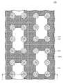
도 1a는 본 발명의 실시예들에 따른 반도체 장치를 나타내는 평면도이다. 도 1b는 도 1a의 I-I'선에 따른 단면도이다.1A is a plan view showing a semiconductor device according to embodiments of the present invention. 1B is a cross-sectional view taken along the line I-I 'in FIG. 1A.
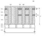
도 1a 및 도 1b를 참조하면, 반도체 장치(100)는 기판(110), 하부 절연막(112), 콘택 플러그들(114), 식각 저지막(120), 하부 전극들(130), 하부 지지 패턴(140), 상부 지지 패턴(145), 유전막(150), 및 상부 전극(160)을 포함할 수 있다. 하부 전극들(130), 유전막(150), 및 상부 전극(160)은 캐패시터(capacitor)를 구성할 수 있으며, 상기 캐패시터의 정전 용량은 하부 전극들(130) 및 상부 전극(160) 사이에 개재되는 유전막(150)의 면적에 비례할 수 있다.1A and 1B, a
기판(110)은 반도체 기판, 예를 들어, 실리콘(Si) 기판, 게르마늄(Ge) 기판, 또는 실리콘-게르마늄(Si-Ge) 기판일 수 있다. 도시하지 않았으나, 기판(110) 상에는 서로 교차하는 복수개의 워드 라인들(미도시) 및 비트 라인들(미도시)이 배치될 수 있으며, 각각의 워드 라인들의 양 옆의 기판(110) 내에는 도핑 영역들이 배치될 수 있다.The
하부 절연막(112)은 기판(110) 상에 배치될 수 있다. 하부 절연막(112)은 절연 물질을 포함할 수 있다. 예를 들어, 하부 절연막(112)은 실리콘 산화물, 실리콘 질화물, 및 실리콘 산질화물 중에서 적어도 하나를 포함할 수 있다.The lower
콘택 플러그들(114)의 각각은 하부 절연막(112)을 관통할 수 있다. 콘택 플러그들(114)의 각각은 기판(110) 내의 상기 도핑 영역들(미도시) 중 어느 하나에 전기적으로 연결될 수 있다. 콘택 플러그들(114)은 도전성 물질을 포함할 수 있다. 일 예로, 콘택 플러그들(114)은 불순물이 도핑된 반도체 물질(예를 들어, 도핑된 다결정 실리콘), 금속-반도체 화합물(예를 들어, 텅스텐 실리사이드), 도전성 금속질화물(예를 들어, 티타늄 질화물, 탄탈늄 질화물, 또는 텅스텐 질화물), 또는 금속(예를 들어, 티타늄, 텅스텐, 또는 탄탈늄) 중에서 적어도 하나를 포함할 수 있다.Each of the contact plugs 114 may penetrate the lower insulating
식각 저지막(120)은 하부 절연막(112) 상에 배치될 수 있다. 식각 저지막(120)은, 일 예로, 실리콘 질화물 또는 실리콘 산질화물을 포함할 수 있다. 몇몇 실시예들에서, 식각 저지막(120)은 생략될 수 있다.The
하부 전극들(130)은 하부 절연막(112) 상에 배치될 수 있다. 하부 전극들(130)의 각각은 식각 저지막(120)을 관통하여 콘택 플러그들(114)의 각각에 전기적으로 연결될 수 있다. 몇몇 실시예들에 따르면, 도 1a에 도시된 바와 같이, 평면적 관점에서 하부 전극들(130)은 행 방향 및 열 방향으로 배열될 수 있다. 하지만, 이에 한정되는 것은 아니며, 다른 실시예들에 따르면, 평면적 관점에서 하부 전극들(130)은 지그재그(zigzag)로 배열될 수 있다.The
하부 전극들(130)의 각각은 기판(110)의 상면에 수직한 방향으로 연장될 수 있다. 몇몇 실시예들에 따르면, 도 1a 및 도 1b에 도시된 바와 같이, 하부 전극들(130)의 각각은 하부가 막힌 실린더(cylinder) 형태를 가질 수 있다. 하지만, 이에 한정되는 것은 아니며, 하부 전극들(130)의 각각은 다양한 형태, 예를 들어 필라(pillar) 형태를 가질 수 있다. 이하, 본 발명의 실시예들에 따른 반도체 장치를 설명하기 위한 도면들은 상기 하부 전극들(130)이 실린더 형태인 경우를 일례로 도시하였다.Each of the
하부 전극들(130)이 실린더 형태인 경우, 하부 전극들(130)의 각각은 기판(110)에 평행하게 연장되는 평판부 및 상기 평판부의 가장자리로부터 위로 연장되는 측벽부를 포함할 수 있다. 하부 전극들(130)의 상기 평판부의 하부 면은 콘택 플러그(114)의 상부 면과 접할 수 있다.When the
하부 전극들(130)은 도전성 물질을 포함할 수 있다. 일 예로, 하부 전극들(130)은 불순물이 도핑된 반도체 물질(예를 들어, 도핑된 다결정 실리콘), 도전성 금속질화물(예를 들어, 티타늄 질화물, 탄탈늄 질화물, 또는 텅스텐 질화물), 금속(예를 들어, 루세늄, 이리듐, 티타늄, 또는 탄탈늄), 또는 도전성 금속산화물(예를 들어, 산화 이리듐) 중에서 적어도 하나를 포함할 수 있다.The
본 발명의 실시예들에 따른 반도체 장치에 의하면, 캐패시터의 정전용량(capacitance)은 하부 전극(130)의 표면적에 비례한다. 따라서, 제한된 면적 내에 형성되는 하부 전극(130)의 표면적을 증가시키기 위해 하부 전극들(130)의 높이(DT)가 증가될 수 있다. 이에 따라, 캐패시터의 정전 용량이 증가될수록 하부 전극(130)의 종횡비(하부 전극의 폭에 대한 하부 전극의 높이 비)가 증가될 수 있다. 하부 전극들(130)의 높이(DT)는, 일 예로, 약 700nm 내지 약 1300nm일 수 있다.According to the semiconductor device according to the embodiments of the present invention, the capacitance of the capacitor is proportional to the surface area of the
하부 지지 패턴(140) 및 상부 지지 패턴(145)은 식각 저지막(120) 상에 배치될 수 있다. 상부 지지 패턴(145)은 기판(110)의 상면에 수직한 방향으로 연장된 하부 전극들(130)의 상부에 인접하게 배치될 수 있고, 하부 지지 패턴(140)은 상부 지지 패턴(145)과 식각 저지막(120) 사이에 배치될 수 있다. 하부 및 상부 지지 패턴들(140, 145)은 하부 전극들(130)의 측벽 일부와 접할 수 있다. 이를 통해, 하부 및 상부 지지 패턴들(140, 145)은 하부 전극들(130)을 수평적으로 지지하여 하부 전극들(130)의 휨 또는 쓰러짐을 방지할 수 있다. 하부 전극들(130)을 지지하는 패턴들은 2개인 것으로 도시되어 있으나 이에 한정되는 것은 아니다. 몇몇 실시예들에 따르면, 추가적인 지지 패턴들(미도시)이 식각 저지막(120) 상에 제공될 수 있다. 이와 달리, 다른 실시예들에 따르면, 하부 지지 패턴(140)은 생략될 수 있다.The
상부 지지 패턴(145)은 소정의 영역에서 제1 개구부들(145a)을 가질 수 있다. 제1 개구부들(145a)은 직사각형 형태, 바(bar) 형태, 또는 라인 형태일 수 있으나, 이에 한정되는 것은 아니며 다양하게 변형될 수 있다. 도 1a에는 제1 개구부들(145a)이 직사각형 형태인 경우가 도시되어 있다.The
하부 지지 패턴(140)은 소정의 영역에서 제2 개구부들(미도시)을 가질 수 있다. 제1 개구부들(145a)와 마찬가지로, 제2 개구부들(미도시)은 직사각형 형태, 바(bar) 형태, 또는 라인 형태일 수 있으나, 이에 한정되는 것은 아니며 다양하게 변형될 수 있다. 평면적 관점에서, 제2 개구부들(미도시)은 제1 개구부들(145a)와 중첩될 수 있다.The
지지 패턴들(140, 145)의 두께가 커질수록, 지지 패턴들(140, 145)이 하부 전극들(130)을 지지하는 강도는 커진다. 하지만, 지지 패턴들(140, 145)의 두께가 커질수록, 하부 전극들(130)과 상부 전극(160) 사이에 개재되는 유전막(150)의 면적이 감소하여 캐패시터의 정전 용량은 작아질 수 있다. 따라서, 지지 패턴들(140, 145)의 두께는 상기 두 인자(강도 및 정전 용량)을 고려하여 결정될 수 있다. 일 예로, 상부 지지 패턴(145)의 두께(TH1)는 약 70nm 내지 약 140nm일 수 있으며, 하부 지지 패턴(140)의 두께(TH2)는 상부 지지 패턴(145)의 두께(TH1)보다 작거나 같을 수 있다. 달리 말해, 상부 지지 패턴(145)의 두께(TH1)는 하부 전극들(130)의 각각의 높이(DT)의 7% 내지 14%일 수 있으며, 하부 지지 패턴(140)의 두께(TH2)는 하부 전극들(130)의 각각의 높이(DT)의 7%이하일 수 있다. 하부 지지 패턴(140) 및 상부 지지 패턴(145)은 SiCN을 포함할 수 있다.As the thickness of the
유전막(150)은 하부 전극들(130)의 표면 상에 균일한 두께로 형성될 수 있다. 유전막(150)은 하부 및 상부 지지 패턴들(140, 145)의 표면, 및 식각 저지막(120)의 상면 상으로 연장될 수 있으며 그 두께는 균일할 수 있다. 유전막(150)은, 일 예로, 금속 산화물(예를 들어, HfO2, ZrO2, Al2O3, La2O3, Ta2O3, 또는 TiO2)과 페브로스카이트(perovskite) 구조의 유전 물질(예를 들어, SrTiO3(STO), (Ba,Sr)TiO3(BST), BaTiO3, PZT, 또는 PLZT) 중에서 선택된 어느 하나의 단일막 또는 이들 막의 조합으로 형성될 수 있다. 유전막(150)은, 일 예로, 약 5nm 내지 약 15nm의 두께를 가질 수 있다.The
상부 전극(160)은 유전막(150) 상에 형성되어 하부 전극들(130)을 덮을 수 있다. 도 1a 및 도 1b에 도시된 바와 같이, 하부 전극들(130)의 각각이 실린더 형태를 갖는 경우, 상부 전극(160)은 상기 실린더의 내부를 채울 수 있다. 이에 따라, 상부 전극(160) 및 하부 전극들(130)의 각각 사이에는 유전막(150)이 개재될 수 있다. 상부 전극(160)은 도전성 물질을 포함할 수 있다. 일 예로, 상부 전극(160)은 불순물이 도핑된 반도체 물질(예를 들어, 도핑된 다결정 실리콘), 도전성 금속질화물(예를 들어, 티타늄 질화물, 탄탈늄 질화물, 또는 텅스텐 질화물), 금속(예를 들어, 루세늄, 이리듐, 티타늄, 또는 탄탈늄), 또는 도전성 금속산화물(예를 들어, 산화 이리듐) 중에서 적어도 하나를 포함할 수 있다.The
도 2 내지 도 9는 본 발명의 실시예들에 따른 반도체 장치의 제조 방법을 나타내는 단면도들로서, 도 1a의 I-I'선에 대응한다. 도 1a 및 도 1b를 참조하여 설명한 본 발명의 실시예들에 따른 반도체 장치와 실질적으로 동일한 구성에 대하여는 동일한 참조 번호가 제공되며, 설명의 간소화를 위하여 중복되는 설명은 생략될 수 있다.FIGS. 2 to 9 are cross-sectional views illustrating a method of manufacturing a semiconductor device according to embodiments of the present invention, corresponding to line I-I 'in FIG. 1A. The same reference numerals are given to substantially the same configurations as those of the semiconductor device according to the embodiments of the present invention described with reference to FIGS. 1A and 1B, and redundant description may be omitted for the sake of simplicity of description.
도 2를 참조하면, 기판(110) 상에 하부 절연막(112)이 형성될 수 있다. 기판(110)은 반도체 기판, 예를 들어, 실리콘(Si) 기판, 게르마늄(Ge) 기판, 또는 실리콘-게르마늄(Si-Ge) 기판일 수 있다. 도시하지 않았으나, 기판(110) 상에는 서로 교차하는 복수개의 워드 라인들(미도시) 및 비트 라인들(미도시)이 형성될 수 있으며, 각각의 워드 라인들의 양 옆의 기판(110) 내에는 도핑 영역들이 형성될 수 있다. 하부 절연막(112)은 실리콘 산화물, 실리콘 질화물, 및 실리콘 산질화물 중에서 적어도 하나를 포함할 수 있다.Referring to FIG. 2, a lower insulating
기판(110) 상에 하부 절연막(112)을 관통하는 콘택 플러그들(114)이 형성될 수 있다. 콘택 플러그들(114)을 형성하는 것은 하부 절연막(112)을 관통하는 콘택 홀들을 형성하는 것, 상기 콘택 홀들을 채우는 도전 층(미도시)을 형성하는 것, 및 하부 절연막(112)의 상면이 노출될 때까지 상기 도전 층(미도시)을 평탄화하는 것을 포함할 수 있다. 콘택 플러그들(114)은 도전성 물질을 포함할 수 있다. 일 예로, 콘택 플러그들(114)은 불순물이 도핑된 반도체 물질(예를 들어, 도핑된 다결정 실리콘), 금속-반도체 화합물(예를 들어, 텅스텐 실리사이드), 도전성 금속질화물(예를 들어, 티타늄 질화물, 탄탈늄 질화물, 또는 텅스텐 질화물), 또는 금속(예를 들어, 티타늄, 텅스텐, 또는 탄탈늄) 중에서 적어도 하나를 포함할 수 있다.Contact plugs 114 penetrating the lower insulating
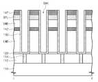
하부 절연막(112) 상에, 식각 저지막(120), 하부 몰드막(LMD), 하부 지지막(142), 상부 몰드막(UMD), 보잉 방지막(BPL), 및 상부 지지막(147)이 차례로 형성될 수 있다. 상기 막들(120, MLD, 142, UMD, BPL, 및 147)의 각각은 화학 기상 증착법(Chemical Vapor Deposition: CVD)에 의해 형성될 수 있다.The lower mold film LMD, the
식각 저지막(120)은 하부 몰드막(LMD)에 대하여 습식 식각 선택성을 갖는 물질을 포함할 수 있다. 일 예로, 식각 저지막(120)은 실리콘 질화물 또는 실리콘 산질화물을 포함할 수 있다. 하부 몰드막(LMD) 및 상부 몰드막(UMD)은 실리콘 산화물을 포함할 수 있다. 하부 지지막(142) 및 상부 지지막(147)은 SiCN을 포함할 수 있다. 보잉 방지막(BPL)은 Si(1-x)Nx를 포함할 수 있으며, 0.51<x<0.55일 수 있다. 몇몇 실시예들에 따르면, 보잉 방지막(BPL)을 형성하는 것은 O 또는 P를 도핑하는 것을 포함할 수 있으며, 이에 따라, 보잉 방지막(BPL)은 O가 도핑된 Si(1-x)Nx, 또는 P가 도핑된 Si(1-x)Nx를 포함할 수 있다.The
상부 지지막(147)의 두께(TH1)와 보잉 방지막(BPL)의 두께(TH3)의 합(TH4)은 상기 막들(120, MLD, 142, UMD, BPL, 및 147)의 전체 두께(DT)의 약 15% 내지 25%일 수 있다. 상부 지지막(147)의 두께(TH1)는 상기 막들(120, MLD, 142, UMD, BPL, 및 147)의 전체 두께(DT)의 약 7% 내지 14%일 수 있다.The sum TH4 of the thickness TH1 of the
구체적으로, 상부 지지막(147)의 두께(TH1)와 보잉 방지막(BPL)의 두께(TH3)의 합(TH4)은 약 150nm 내지 약 250nm일 수 있고, 상부 지지막(147)의 두께(TH1)는 약 70nm 내지 약 140nm일 수 있다. 하부 지지막(142)의 두께(TH2)는 상부 지지막(147)의 두께(TH1)와 같거나 작을 수 있다. 상기 막들(120, MLD, 142, UMD, BPL, 및 147)의 전체 두께(DT)는 약 700nm 내지 약 1300nm일 수 있다.More specifically, the sum TH4 of the thickness TH1 of the
도 3을 참조하면, 식각 저지막(120), 하부 몰드막(LMD), 하부 지지막(142), 상부 몰드막(UMD), 보잉 방지막(BPL), 및 상부 지지막(147)을 관통하는 스토리지 노드 홀들(SNH)이 형성될 수 있다. 스토리지 노드 홀들(SNH)을 형성하는 것은 건식 식각 공정을 이용하여 수행될 수 있다. 스토리지 노드 홀들(SNH)에 의해 콘택 플러그들(114)이 노출될 수 있다. 스토리지 노드 홀들(SNH)의 각각의 깊이(DT)는 상기 막들(120, MLD, 142, UMD, BPL, 및 147)의 전체 두께(DT)와 동일할 수 있으며, 약 700nm 내지 약 1300nm일 수 있다.Referring to FIG. 3, the
하부 지지막(142) 및 상부 지지막(147)은 SiCN을 포함하고, 보잉 방지막(BPL)은 Si(1-x)Nx(0.51<x<0.55)를 포함하며, 하부 몰드막(LMD) 및 상부 몰드막(UMD)은 실리콘 산화물을 포함하는 경우, 상기 건식 식각 공정에 대하여, 보잉 방지막(BPL)은 하부 지지막(142) 및 상부 지지막(147)과 실질적으로 동일한 식각 속도를 가질 수 있다. 예를 들어, 상기 건식 식각 공정에 대하여, 보잉 방지막(BPL)의 식각 속도는 하부 지지막(142) 및 상부 지지막(147)의 식각 속도의 0.8배 내지 1.2배일 수 있다. 이와 달리, 상기 건식 식각 공정에 대하여, 하부 몰드막(LMD) 및 상부 몰드막(UMD)의 식각 속도는 보잉 방지막(BPL), 하부 지지막(142) 및 상부 지지막(147)의 식각 속도보다 클 수 있다.The
보잉 방지막(BPL)을 포함하지 않는 일반적인 반도체 장치의 제조 방법에 따르면, 건식 식각 공정을 이용하여 스토리지 노드 홀(SNH)들을 형성하는 공정에서, 실리콘 산화물을 포함하는 하부 몰드막(LMD) 및 상부 몰드막(UMD)의 식각 속도는 SiCN을 포함하는 하부 지지막(142) 및 상부 지지막(147)의 식각 속도보다 크다. 이에 따라, 건식 식각 공정이 길어지면, 상부 몰드막(UMD)의 측벽 중 일부가 움푹 파이는 보잉(bowing) 현상이 발생할 수 있다. 특히, 스토리지 노드 홀들(SNH)의 깊이(DT)가 약 700nm 내지 약 1300nm와 같이 깊은 경우, 건식 식각 공정 시간이 길어져 보잉 현상이 발생할 확률은 높아진다. 이는, 상부 몰드막(UMD)이 상기 건식 식각 공정에 오래 노출되기 때문일 수 있다. 건식 식각 공정에 대하여, 낮은 식각 속도를 갖는 상부 지지막(147)의 두께(TH1)를 크게 하면(예를 들어, 약 150nm 내지 약 250nm, 혹은 스토리지 노드 홀(SNH)의 깊이(DT)의 15% 내지 25%) 보잉 현상은 억제될 수 있으나, 커진 두께에 해당하는 만큼 캐패시터의 정전 용량이 작아진다.According to a general method of manufacturing a semiconductor device that does not include a BOE (BPL), in a process of forming storage node holes (SNHs) using a dry etching process, a lower mold film (LMD) The etch rate of the film UMD is greater than the etch rate of the
본 발명의 실시예들에 따른 반도체 장치의 제조 방법에 의하면, 보잉 방지막(BPL)이 상부 지지막(147)과 상부 몰드막(UMD) 사이에 형성될 수 있다. 상기 건식 식각 공정에 대하여, 보잉 방지막(BPL)은 상부 지지막(147)과 실질적으로 동일한 식각 속도를 가지므로 (즉, 상부 몰드막(UMD)보다 낮은 식각 속도를 가지므로), 보잉 방지막(BPL)은 상부 지지막(147)과 함께, 건식 식각 공정이 수행되는 동안에 보잉 현상이 발생하는 것을 방지할 수 있다. 이에 따라, 상부 지지막(147)의 두께(TH1)와 보잉 방지막(BPL)의 두께(TH3)의 합(TH4)을 충분히 크게 함으로써(예를 들어, 약 150nm 내지 약 250nm, 혹은 스토리지 노드 홀(SNH)의 깊이(DT)의 15% 내지 25%) 보잉 현상을 억제할 수 있다.According to the method for manufacturing a semiconductor device according to the embodiments of the present invention, the BOE prevention film BPL can be formed between the
나아가, 본 발명의 실시예들에 따른 반도체 장치의 제조 방법에 의하면, 후술할 바와 같이, 보잉 방지막(BPL)은 하부 몰드막(LMD) 및 상부 몰드막(UMD)을 제거하는 후속 습식 식각 공정에서 제거될 수 있다. 따라서, 보잉 방지막(BPL)의 두께(TH3)에 해당하는 만큼 캐패시터의 정전 용량이 증가될 수 있다.Further, according to the method of manufacturing a semiconductor device according to embodiments of the present invention, as described later, the BoN prevention film (BPL) is formed in a subsequent wet etching process for removing the lower mold film LMD and the upper mold film UMD Can be removed. Accordingly, the capacitance of the capacitor can be increased by the thickness TH3 of the bowing prevention film BPL.
도 4를 참조하면, 스토리지 노드 홀들(SNH) 내에 하부 전극들(130)이 형성될 수 있다. 하부 전극들(130)을 형성하는 것은 스토리지 노드 홀들(SNH)의 내벽을 덮도록 하부 전극막(미도시)을 증착하는 것 및 상부 지지막(147)의 상면이 노출될 때까지 상기 하부 전극막을 평탄화 하는 것을 포함할 수 있다. 상기 평탄화 공정은 화학적-기계적 연마(chemical-mechenical polishing: CMP)를 이용하여 수행될 수 있다.Referring to FIG. 4, the
상기 하부 전극막은 물리 기상 증착법(Physical Vapor Deposition: PVD) 또는 화학 기상 증착법(Chemical Vapor Deposition: CVD)을 이용하여 형성될 수 있다. 하부 전극들(130)은 도전성 물질을 포함할 수 있다. 일 예로, 하부 전극들(130)은 불순물이 도핑된 반도체 물질(예를 들어, 도핑된 다결정 실리콘), 도전성 금속질화물(예를 들어, 티타늄 질화물, 탄탈늄 질화물, 또는 텅스텐 질화물), 금속(예를 들어, 루세늄, 이리듐, 티타늄, 또는 탄탈늄), 또는 도전성 금속산화물(예를 들어, 산화 이리듐) 중에서 적어도 하나를 포함할 수 있다.The lower electrode film may be formed using physical vapor deposition (PVD) or chemical vapor deposition (CVD). The
하부 전극들(130)의 각각은 콘택 플러그들(114)의 각각에 전기적으로 연결될 수 있다.Each of the
도 5를 참조하면, 상부 지지막(147) 및 보잉 방지막(BPL)을 패터닝함으로써 상부 지지 패턴(145) 및 보잉 방지 패턴(BPP)이 형성될 수 있다. 도 1a에 도시된 바와 같이, 상부 지지 패턴(145)은 개구부들(145a)을 가질 수 있다. 도시되지는 않았으나, 보잉 방지 패턴(BPP)도 평면적 관점에서 상부 지지 패턴(145)의 개구부들(145a)와 중첩되는 개구부들(미도시)을 가질 수 있다. 상부 지지 패턴(145)의 개구부들(145a) 및 보잉 방지 패턴(BPP)의 상기 개구부들에 의하여 상부 몰드막(UMD)의 일부가 노출될 수 있다. 상부 지지막(147) 및 보잉 방지막(BPL)을 패터닝하는 것은 건식 식각 공정에 의해 수행될 수 있다.Referring to FIG. 5, the
도 6을 참조하면, 습식 식각 공정을 이용하여 상부 몰드막(UMD)이 제거될 수 있다. 상기 습식 식각 공정을 HF 및 NH4F를 포함하는 LAL(Low Ammoniumfluoride Liquid) 용액을 이용하여 수행될 수 있다.Referring to FIG. 6, the upper mold film (UMD) can be removed using a wet etching process. It may be performed using the LAL (Low Ammoniumfluoride Liquid) solution for the wet etching process including HF and NH4 F.
상부 지지 패턴(145)은 SiCN을 포함하고, 보잉 방지 패턴(BPP)은 Si(1-x)Nx(0.51<x<0.55)를 포함하며, 상부 몰드막(UMD)은 실리콘 산화물을 포함하는 경우, 상기 습식 식각 공정에 대하여, 보잉 방지 패턴(BPP)은 상부 지지 패턴(145)보다 큰 식각 속도를 가질 수 있다. 또한, 상기 습식 식각 공정에 대하여, 상부 몰드막(UMD)의 식각 속도는 보잉 방지 패턴(BPP)의 식각 속도와 같거나 클 수 있다.The
구체적으로, 상기 습식 식각 공정에 대하여, 보잉 방지 패턴(BPP)의 식각 속도는 상부 지지 패턴(145)의 식각 속도의 20배 내지 500배일 수 있고, 상부 몰드막(UMD)의 식각 속도는 보잉 방지 패턴(BPP)의 식각 속도의 1배 내지 20배일 수 있다.Specifically, in the wet etching process, the etching rate of the anti-bowing pattern BPP may be 20 to 500 times the etching rate of the
더 구체적으로, 상기 습식 식각 공정에 대하여, 상부 지지 패턴(145)의 식각 속도는 약 1nm/min 내지 약 2.5nm/min일 수 있고, 보잉 방지 패턴(BPP)의 식각 속도는 약 50nm/min 내지 약 500nm/min일 수 있고, 그리고 상부 몰드막(UMD)의 식각 속도는 약 500nm/min 내지 약 1000nm/min일 수 있다.More specifically, for the wet etch process, the etch rate of the
상기 습식 식각 공정에 의하여, 보잉 방지 패턴(BPP)의 적어도 일부가 함께 제거될 수 있다. 몇몇 실시예에 따르면, 도 6에 도시된 바와 같이, 보잉 방지 패턴(BPP)의 일부만 제거되어 잔류 보잉 방지 패턴(RBPP)이 형성될 수 있다. 다른 실시예들에 따르면, 도 6에 도시된 바와 달리, 보잉 방지 패턴(BPP)이 완전히 제거될 수 있다.By the wet etching process, at least a part of the anti-bowing pattern (BPP) can be removed together. According to some embodiments, as shown in FIG. 6, only a part of the anti-flying pattern BPP may be removed to form the remaining anti-flying pattern RBPP. According to other embodiments, unlike the one shown in Fig. 6, the anti-bowing pattern BPP can be completely removed.
도 7을 참조하면, 하부 지지막(142)을 패터닝함으로써 하부 지지 패턴(140)이 형성될 수 있다. 하부 지지 패턴(140)은 상부 지지 패턴(145)의 개구부들(도 1a의 145a)와 중첩되는 개구부들을 가질 수 있다. 하부 지지 패턴(140)의 개구부들에 의해 하부 몰드막(LMD)의 일부가 노출될 수 있다. 하부 지지막(142)을 패터닝하는 것은 건식 식각 공정에 의해 수행될 수 있다.Referring to FIG. 7, the lower supporting
도 8을 참조하면, 습식 식각 공정을 이용하여 하부 몰드막(LMD)이 제거될 수 있다. 상기 습식 식각 공정을 HF 및 NH4F를 포함하는 LAL 용액을 이용하여 수행될 수 있다.Referring to FIG. 8, the lower mold film (LMD) can be removed using a wet etching process. The wet etching process may be performed using a LAL solution containing HF and NH4 F.
하부 및 상부 지지 패턴들(140, 145)은 SiCN을 포함하고, 잔류 보잉 방지 패턴(RBPP)은 Si(1-x)Nx(0.51<x<0.55)를 포함하며, 하부 몰드막(LMD)은 실리콘 산화물을 포함하는 경우, 상기 습식 식각 공정에 대하여, 잔류 보잉 방지 패턴(RBPP)은 하부 및 상부 지지 패턴들(140, 145)보다 큰 식각 속도를 가질 수 있다. 또한, 상기 습식 식각 공정에 대하여, 하부 몰드막(LMD)의 식각 속도는 잔류 보잉 방지 패턴(RBPP)의 식각 속도와 같거나 클 수 있다.The lower and
구체적으로, 상기 습식 식각 공정에 대하여, 잔류 보잉 방지 패턴(RBPP)의 식각 속도는 하부 및 상부 지지 패턴들(140, 145)의 식각 속도의 20배 내지 500배일 수 있고, 하부 몰드막(LMD)의 식각 속도는 잔류 보잉 방지 패턴(RBPP)의 식각 속도의 1배 내지 20배일 수 있다.Specifically, in the wet etching process, the etch rate of the residual anti-bowing pattern RBPP may be 20 to 500 times the etch rate of the lower and
더 구체적으로, 상기 습식 식각 공정에 대하여, 하부 및 상부 지지 패턴들(140, 145)의 식각 속도는 약 1nm/min 내지 약 2.5nm/min일 수 있고, 잔류 보잉 방지 패턴(RBPP)의 식각 속도는 약 50nm/min 내지 약 500nm/min일 수 있고, 그리고 하부 몰드막(LMD)의 식각 속도는 약 500nm/min 내지 약 1000nm/min일 수 있다.More specifically, for the wet etching process, the etch rate of the lower and
도 6 및 7에 도시된 바와 같이, 잔류 보잉 방지 패턴(RBPP)이 존재하는 경우, 상기 습식 식각 공정에 의하여, 잔류 보잉 방지 패턴(RBPP)이 제거될 수 있다.As shown in FIGS. 6 and 7, when the remaining anti-flying pattern (RBPP) is present, the residual anti-flying pattern (RBPP) can be removed by the wet etching process.
도 5 내지 8을 참조하여 설명한 일련의 공정들을 통하여, 하부 전극들(130)이 노출될 수 있다.Through the series of processes described with reference to FIGS. 5 to 8, the
도 9를 참조하면, 노출된 하부 전극들(130)을 덮는 유전막(150)이 형성될 수 있다. 유전막(150)은 하부 전극들(130)의 표면, 하부 및 상부 지지 패턴들(140, 145)의 표면, 및 식각 저지막(120)의 상면을 따라 컨포말하게 형성될 수 있다. 유전막(150)은, 일 예로, 금속 산화물(예를 들어, HfO2, ZrO2, Al2O3, La2O3, Ta2O3, 또는 TiO2)과 페브로스카이트(perovskite) 구조의 유전 물질(예를 들어, SrTiO3(STO), (Ba,Sr)TiO3(BST), BaTiO3, PZT, 또는 PLZT) 중에서 선택된 어느 하나의 단일막 또는 이들 막의 조합으로 형성될 수 있다. 그리고 유전막(150)은, 일 예로, 약 5nm 내지 약 15nm의 두께를 가질 수 있다. 유전막(150)은 물리 기상 증착법(Physical Vapor Deposition: PVD) 또는 원자층 증착법(Atomic Layer Deposition: ALD)을 이용하여 형성될 수 있다.Referring to FIG. 9, a
도 1b를 다시 참조하면, 유전막(150)을 덮는 상부 전극(160)이 형성될 수 있다. 상부 전극(160)은 도전성 물질을 포함할 수 있다. 일 예로, 상부 전극(160)은 불순물이 도핑된 반도체 물질(예를 들어, 도핑된 다결정 실리콘), 도전성 금속질화물(예를 들어, 티타늄 질화물, 탄탈늄 질화물, 또는 텅스텐 질화물), 금속(예를 들어, 루세늄, 이리듐, 티타늄, 또는 탄탈늄), 또는 도전성 금속산화물(예를 들어, 산화 이리듐) 중에서 적어도 하나를 포함할 수 있다. 상부 전극(160)은 물리 기상 증착법(Physical Vapor Deposition: PVD) 또는 원자층 증착법(Atomic Layer Deposition: ALD)을 이용하여 형성될 수 있다.Referring again to FIG. 1B, an
하부 전극들(130), 유전막(150), 및 상부 전극(160)은 캐패시터를 구성할 수 있으며, 상기 캐패시터의 정전 용량은 하부 전극들(130) 및 상부 전극(160) 사이에 개재되는 유전막(150)의 면적에 비례할 수 있다.The
본 발명의 실시예들에 따른 반도체 장치의 제조 방법에 의하면, 보잉 방지막(BPL)이 상부 지지막(147)과 상부 몰드막(UMD) 사이에 형성될 수 있다. 건식 식각 공정에 대하여, 보잉 방지막(BPL)은 상부 지지막(147)과 실질적으로 동일한 식각 속도를 가지되, 상부 몰드막(UMD) 및 하부 몰드막(LMD)보다 작은 식각 속도를 가질 수 있다. 이에 따라, 스토리지 노드 홀들(SNH)을 형성하는 건식 식각 공정에서, 보잉 방지막(BPL)은 보잉 현상이 발생하는 것을 억제할 수 있다.According to the method for manufacturing a semiconductor device according to the embodiments of the present invention, the BOE prevention film BPL can be formed between the
나아가, 습식 식각 공정에 대하여, 보잉 방지막(BPL)은 하부 및 상부 지지 패턴들(140, 145)보다 큰 식각 속도를 가질 수 있다. 이에 따라, 보잉 방지막(BPL)은 하부 몰드막(LMD) 및 상부 몰드막(UMD)을 제거하는 후속 습식 식각 공정에서 제거될 수 있다. 보잉 방지막(BPL)의 두께(TH3)에 해당하는 만큼 캐패시터의 정전 용량이 증가될 수 있다.Further, with respect to the wet etching process, the anti-bowing film (BPL) may have an etching rate larger than that of the lower and
도 10은 본 발명의 실시예들에 따른 반도체 장치를 포함하는 메모리 시스템의 일 예를 나타내는 개략 블록도이다.10 is a schematic block diagram illustrating an example of a memory system including a semiconductor device according to embodiments of the present invention.
도 10을 참조하면, 본 발명의 일 실시 예에 따른 메모리 시스템(1100)은 컨트롤러(1110), 입출력 장치(1120, I/O), 기억 장치(1130, memory device), 인터페이스(1140) 및 버스(1150, bus)를 포함할 수 있다. 상기 컨트롤러(1110), 입출력 장치(1120), 기억 장치(1130) 및/또는 인터페이스(1140)는 버스(1150)를 통하여 서로 결합 될 수 있다. 버스(1150)는 데이터들이 이동되는 통로(path)에 해당한다. 컨트롤러(1110), 입출력 장치(1120, I/O), 기억 장치(1130, memory device), 및/또는 인터페이스(1140)은 본 발명의 실시예들에 따른 반도체 장치를 포함할 수 있다.10, a
컨트롤러(1110)는 마이크로프로세서, 디지털 신호 프로세스, 마이크로컨트롤러, 및 이들과 유사한 기능을 수행할 수 있는 논리 소자들 중에서 적어도 하나를 포함할 수 있다. 입출력 장치(1120)는 키패드(keypad), 키보드 및 디스플레이 장치등을 포함할 수 있다. 기억 장치(1130)는 데이터 및/또는 명령어등을 저장할 수 있다. 인터페이스(1140)는 통신 네트워크로 데이터를 전송하거나 통신 네트워크로부터 데이터를 수신하는 기능을 수행할 수 있다. 인터페이스(1140)는 유선 또는 무선 형태일 수 있다. 예컨대, 인터페이스(1140)는 안테나 또는 유무선 트랜시버 등을 포함할 수 있다. 도시하지 않았지만, 메모리 시스템(1100)은 컨트롤러(1110)의 동작을 향상시키기 위한 동작 기억 소자로서, 고속의 디램 소자 및/또는 에스램 소자 등을 더 포함할 수도 있다.The
메모리 시스템(1100)은 개인 휴대용 정보 단말기(PDA, personal digital assistant) 포터블 컴퓨터(portable computer), 웹 타블렛(web tablet), 무선 전화기(wireless phone), 모바일 폰(mobile phone), 디지털 뮤직 플레이어(digital music player), 메모리 카드(memory card), 또는 정보를 무선환경에서 송신 및/또는 수신할 수 있는 모든 전자 제품에 적용될 수 있다.The
도 11은 본 발명의 실시예들에 따른 반도체 장치를 포함하는 따른 전자 시스템의 블록도이다.11 is a block diagram of an accompanying electronic system including a semiconductor device in accordance with embodiments of the present invention.
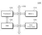
도 11을 참조하면, 전자 시스템(1200)은 본 발명의 실시예들에 따른 반도체 장치를 적어도 하나 포함할 수 있다. 전자 시스템(1200)은 모바일 기기나 컴퓨터 등을 포함할 수 있다. 예를 들어, 전자 시스템(1200)은 메모리 시스템(1210), 프로세서(1220), 램(1230), 및 유저인터페이스(1240)를 포함할 수 있고, 이들은 버스(Bus, 1250)를 이용하여 서로 데이터 통신을 할 수 있다. 프로세서(1220)는 프로그램을 실행하고 전자 시스템(1200)을 제어하는 역할을 할 수 있다. 램(1230)은 프로세서(1220)의 동작 메모리로서 사용될 수 있다. 예를 들어, 프로세서(1220) 및 램(1230)은 각각 본 발명의 실시예들에 따른 반도체 장치를 포함할 수 있다. 이와 달리, 프로세서(1220)와 램(1230)이 하나의 패키지에 포함될 수 있다. 유저 인터페이스(1240)는 전자 시스템(1200)에 데이터를 입력 또는 출력하는데 이용될 수 있다. 메모리 시스템(1210)은 프로세서(1220)의 동작을 위한 코드, 프로세서(1220)에 의해 처리된 데이터 또는 외부에서 입력된 데이터를 저장할 수 있다.Referring to FIG. 11,
상기 전자 시스템(1200)은 모바일 시스템, 개인용 컴퓨터, 산업용 컴퓨터 또는 다양한 기능을 수행하는 로직 시스템 등으로 구현될 수 있다. 예컨대, 상기 모바일 시스템은 개인 휴대용 정보 단말기(PDA; Personal Digital Assistant), 휴대용 컴퓨터, 웹 타블렛(web tablet), 모바일 폰(mobile phone), 무선폰(wireless phone), 랩톱(laptop) 컴퓨터, 메모리 카드, 디지털 뮤직 시스템(digital music system) 그리고 정보 전송/수신 시스템 중 어느 하나일 수 있다. 상기 전자 시스템(1200)이 무선 통신을 수행할 수 있는 장비인 경우에, 상기 전자 시스템(1200)은 CDMA, GSM, NADC, E-TDMA, WCDMA, CDMA2000과 같은 3세대 통신 시스템 같은 통신 인터페이스 프로토콜에서 사용될 수 있다.The
이상, 첨부된 도면을 참조하여 본 발명의 실시예를 설명하였지만, 본 발명이 속하는 기술분야에서 통상의 지식을 가진 자는 본 발명이 그 기술적 사상이나 필수적인 특징을 변경하지 않고서 다른 구체적인 형태로 실시될 수 있다는 것을 이해할 수 있을 것이다. 그러므로 이상에서 기술한 실시예에는 모든 면에서 예시적인 것이며 한정적이 아닌 것으로 이해해야만 한다.While the present invention has been described in connection with what is presently considered to be practical exemplary embodiments, it is to be understood that the invention is not limited to the disclosed embodiments, but, on the contrary, It will be understood. It is therefore to be understood that the above-described embodiments are illustrative and not restrictive in every respect.
Claims (10)
Translated fromKorean건식 식각 공정을 이용하여, 상기 상부 몰드막, 상기 보잉 방지막, 및 상기 상부 지지막을 관통하는 스토리지 노드 홀을 형성하는 것;
상기 스토리지 노드 홀 내에 하부 전극을 형성하는 것;
상기 상부 지지막 및 상기 보잉 방지막을 패터닝하여, 상기 상부 몰드막의 일부를 노출하는 것;
제1 습식 식각 공정을 이용하여, 상기 상부 몰드막 및 상기 보잉 방지막을 제거하는 것; 및
상기 하부 전극을 덮는 유전막 및 상부 전극을 차례로 형성하는 것을 포함하되,
상기 건식 식각 공정에 대하여, 상기 보잉 방지막은 상기 상부 지지막과 실질적으로 동일한 식각 속도를 가지고,
상기 제1 습식 식각 공정에 대하여, 상기 보잉 방지막은 상기 상부 지지막보다 큰 식각 속도를 가지고,
상기 상부 지지막의 두께와 상기 보잉 방지막의 두께의 합은 상기 스토리지 노드 홀의 깊이의 15% 내지 25%인 반도체 장치의 제조 방법.Forming an upper mold film, a bowing prevention film, and an upper support film in this order on a substrate;
Forming a storage node hole through the upper mold film, the anti-bowing film, and the upper support film using a dry etching process;
Forming a lower electrode in the storage node hole;
Patterning the upper support film and the anti-bowing film to expose a part of the upper mold film;
Removing the upper mold film and the anti-bowing film using a first wet etching process; And
Forming a dielectric film covering the lower electrode and an upper electrode in order,
For the dry etching process, the BOE prevention film has an etching rate substantially the same as that of the upper support film,
In the first wet etching process, the bowing prevention film has a larger etching rate than the upper supporting film,
Wherein the sum of the thickness of the upper support film and the thickness of the anti-bowing film is 15% to 25% of the depth of the storage node hole.
상기 제1 습식 식각 공정에 대하여, 상기 보잉 방지막의 식각 속도는 상기 상부 지지막의 식각 속도의 20배 내지 500배인 반도체 장치의 제조 방법.The method according to claim 1,
Wherein the etching rate of the anti-bowing film is 20 to 500 times the etching rate of the upper support film in the first wet etching step.
상기 제1 습식 식각 공정에 대하여, 상기 보잉 방지막의 식각 속도는 50nm/min 내지 500nm/min인 반도체 장치의 제조 방법.3. The method of claim 2,
Wherein, in the first wet etching step, the etching rate of the anti-bowing film is 50 nm / min to 500 nm / min.
상기 제1 습식 식각 공정에 대하여, 상기 상부 지지막의 식각 속도는 1nm/min 내지 2.5nm/min인 반도체 장치의 제조 방법.3. The method of claim 2,
Wherein, in the first wet etching step, the etching rate of the upper support film is 1 nm / min to 2.5 nm / min.
상기 보잉 방지막은 Si(1-x)Nx를 포함하되, 0.51<x<0.55인 반도체 장치의 제조 방법.The method according to claim 1,
Wherein the BOE prevention film contains Si(1-x) Nx , wherein 0.51 < x < 0.55.
상기 상부 몰드막을 형성하기 전에, 상기 기판 상에 하부 몰드막 및 하부 지지막을 차례로 형성하는 것을 더 포함하되,
상기 스토리지 노드 홀은 상기 하부 몰드막 및 상기 하부 지지막을 관통하는 반도체 장치의 제조 방법.The method according to claim 1,
Further comprising forming a lower mold film and a lower support film on the substrate in order before forming the upper mold film,
And the storage node hole penetrates the lower mold film and the lower support film.
상기 유전막을 형성하기 전에,
상기 하부 지지막을 패터닝하여, 상기 하부 몰드막의 일부를 노출하는 것; 및
제2 습식 식각 공정을 이용하여, 상기 하부 몰드막을 제거하는 것을 더 포함하되,
상기 제1 습식 공정에 의해, 상기 보잉 방지막의 일부가 잔류하고,
상기 제2 습식 공정에 의해, 상기 보잉 방지막의 상기 잔류하는 일부가 제거되는 반도체 장치의 제조 방법.The method according to claim 6,
Before forming the dielectric film,
Patterning the lower support film to expose a portion of the lower mold film; And
Further comprising removing the lower mold film using a second wet etch process,
A part of the bowing prevention film remains by the first wet process,
And the residual portion of the anti-flying film is removed by the second wet process.
상기 상부 몰드막, 상기 보잉 방지막, 및 상기 상부 지지막을 관통하는 스토리지 노드 홀을 형성하는 것;
상기 스토리지 노드 홀 내에 하부 전극을 형성하는 것;
상기 상부 지지막 및 상기 보잉 방지막을 패터닝하여, 상기 상부 몰드막의 일부를 노출하는 것;
상기 상부 몰드막 및 상기 보잉 방지막을 제거하는 것; 및
상기 하부 전극을 덮는 유전막 및 상부 전극을 차례로 형성하는 것을 포함하되,
상기 보잉 방지막은 0.51<x<0.55인 Si(1-x)Nx를 포함하고,
상기 상부 지지막은 SiCN을 포함하는 반도체 장치의 제조 방법.Forming an upper mold film, a bowing prevention film, and an upper support film in this order on a substrate;
Forming a storage node hole through the upper mold film, the anti-bowing film, and the upper support film;
Forming a lower electrode in the storage node hole;
Patterning the upper support film and the anti-bowing film to expose a part of the upper mold film;
Removing the upper mold film and the anti-bowing film; And
Forming a dielectric film covering the lower electrode and an upper electrode in order,
Wherein the BOE prevention film comprises Si(1-x) Nx of 0.51 < x < 0.55,
Wherein the upper support film comprises SiCN.
상기 스토리지 노드 홀을 형성하는 것은 건식 식각 공정을 수행하는 것을 포함하고,
상기 건식 식각 공정에 대하여, 상기 보잉 방지막의 식각 속도는 상기 상부 지지막의 식각 속도와 실질적으로 동일한 반도체 장치의 제조 방법.9. The method of claim 8,
Forming the storage node hole comprises performing a dry etching process,
Wherein the etching rate of the anti-bowing film is substantially the same as the etching rate of the upper support film in the dry etching process.
상기 상부 몰드막 및 상기 보잉 방지막을 제거하는 것은 습식 식각 공정을 수행하는 것을 포함하고,
상기 습식 식각 공정에 대하여, 상기 보잉 방지막의 식각 속도는 상기 상부 지지막의 식각 속도의 20배 내지 500배인 반도체 장치의 제조 방법.
9. The method of claim 8,
Removing the upper mold film and the anti-bowing film comprises performing a wet etching process,
Wherein the etching rate of the anti-bowing film is 20 to 500 times the etching rate of the upper support film in the wet etching process.
Priority Applications (2)
| Application Number | Priority Date | Filing Date | Title |
|---|---|---|---|
| KR1020150089889AKR102279720B1 (en) | 2015-06-24 | 2015-06-24 | Semiconductor device and method for manufacturing the same |
| US15/191,552US9570448B2 (en) | 2015-06-24 | 2016-06-24 | Semiconductor device and method for manufacturing the same |
Applications Claiming Priority (1)
| Application Number | Priority Date | Filing Date | Title |
|---|---|---|---|
| KR1020150089889AKR102279720B1 (en) | 2015-06-24 | 2015-06-24 | Semiconductor device and method for manufacturing the same |
Publications (2)
| Publication Number | Publication Date |
|---|---|
| KR20170000894Atrue KR20170000894A (en) | 2017-01-04 |
| KR102279720B1 KR102279720B1 (en) | 2021-07-22 |
Family
ID=57602723
Family Applications (1)
| Application Number | Title | Priority Date | Filing Date |
|---|---|---|---|
| KR1020150089889AActiveKR102279720B1 (en) | 2015-06-24 | 2015-06-24 | Semiconductor device and method for manufacturing the same |
Country Status (2)
| Country | Link |
|---|---|
| US (1) | US9570448B2 (en) |
| KR (1) | KR102279720B1 (en) |
Cited By (3)
| Publication number | Priority date | Publication date | Assignee | Title |
|---|---|---|---|---|
| KR20180086902A (en)* | 2017-01-24 | 2018-08-01 | 삼성전자주식회사 | Semiconductor device |
| US11056355B2 (en) | 2018-10-04 | 2021-07-06 | Samsung Electronics Co., Ltd. | Semiconductor device and method of fabricating the same |
| CN115020408A (en)* | 2021-03-05 | 2022-09-06 | 长鑫存储技术有限公司 | Semiconductor structure and forming method thereof |
Families Citing this family (14)
| Publication number | Priority date | Publication date | Assignee | Title |
|---|---|---|---|---|
| CN108269789B (en)* | 2016-12-30 | 2022-05-03 | 联华电子股份有限公司 | Capacitor structure and manufacturing method thereof |
| KR102403619B1 (en)* | 2017-09-18 | 2022-05-30 | 삼성전자주식회사 | Semiconductor device and method for manufacturing the same |
| CN110544697B (en) | 2018-05-28 | 2020-12-01 | 联华电子股份有限公司 | Semiconductor memory device and method of forming the same |
| KR102557019B1 (en)* | 2018-07-02 | 2023-07-20 | 삼성전자주식회사 | Semiconductor memory device |
| KR102661837B1 (en) | 2018-07-23 | 2024-05-02 | 삼성전자주식회사 | A semiconductor device |
| CN111326654A (en)* | 2018-12-13 | 2020-06-23 | 夏泰鑫半导体(青岛)有限公司 | Semiconductor device and method for manufacturing the same |
| KR102515421B1 (en)* | 2018-12-20 | 2023-03-28 | 삼성전자주식회사 | Method for fabricating semiconductor device |
| CN117766453A (en)* | 2019-04-08 | 2024-03-26 | 群创光电股份有限公司 | Transfer connector and method for manufacturing electronic device |
| CN112786593B (en)* | 2019-11-11 | 2024-12-10 | 长鑫存储技术有限公司 | Semiconductor device and method for forming the same |
| US11935917B2 (en) | 2020-07-27 | 2024-03-19 | Changxin Memory Technologies, Inc. | Semiconductor structure forming method and semiconductor structure |
| CN113990870B (en)* | 2020-07-27 | 2024-09-20 | 长鑫存储技术有限公司 | Method for forming semiconductor structure and semiconductor structure |
| CN114171464B (en)* | 2020-09-11 | 2024-07-02 | 长鑫存储技术有限公司 | Semiconductor structure and manufacturing method thereof |
| CN114171463B (en)* | 2020-09-11 | 2024-06-21 | 长鑫存储技术有限公司 | Semiconductor structure and manufacturing method thereof |
| TWI799136B (en)* | 2022-02-15 | 2023-04-11 | 力晶積成電子製造股份有限公司 | Method of manufacturing semiconductor device |
Citations (4)
| Publication number | Priority date | Publication date | Assignee | Title |
|---|---|---|---|---|
| KR20120028509A (en)* | 2010-09-15 | 2012-03-23 | 삼성전자주식회사 | Method of forming a capacitor and method of manufacturing a semiconductor device using the same |
| KR20130023770A (en)* | 2011-08-29 | 2013-03-08 | 에스케이하이닉스 주식회사 | Method for fabricating capacitor |
| KR20130100463A (en)* | 2012-03-02 | 2013-09-11 | 삼성전자주식회사 | A semiconductor memory device and a method of forming the same |
| KR20140070739A (en)* | 2012-11-26 | 2014-06-11 | 삼성전자주식회사 | Semiconductor device and method for fabricating the same |
Family Cites Families (12)
| Publication number | Priority date | Publication date | Assignee | Title |
|---|---|---|---|---|
| US7067385B2 (en) | 2003-09-04 | 2006-06-27 | Micron Technology, Inc. | Support for vertically oriented capacitors during the formation of a semiconductor device |
| US7125781B2 (en) | 2003-09-04 | 2006-10-24 | Micron Technology, Inc. | Methods of forming capacitor devices |
| KR100655751B1 (en) | 2004-10-01 | 2006-12-11 | 삼성전자주식회사 | Manufacturing Method of Semiconductor Device |
| KR100885922B1 (en) | 2007-06-13 | 2009-02-26 | 삼성전자주식회사 | Semiconductor element and method of forming the semiconductor element |
| KR101357303B1 (en) | 2007-07-10 | 2014-01-28 | 삼성전자주식회사 | Semiconductor device and method of fabricating the same semiconductor |
| KR20100078971A (en) | 2008-12-30 | 2010-07-08 | 주식회사 하이닉스반도체 | Semiconductor device and method for manufacturing of the same |
| KR101111922B1 (en) | 2009-08-18 | 2012-06-27 | 주식회사 하이닉스반도체 | Semiconductor device and method of manufacturing the same |
| KR20130049393A (en) | 2011-11-04 | 2013-05-14 | 에스케이하이닉스 주식회사 | Method for fabricating semiconductor device |
| US20130228837A1 (en) | 2012-03-01 | 2013-09-05 | Elpida Memory, Inc. | Semiconductor device |
| KR101934421B1 (en) | 2012-11-13 | 2019-01-03 | 삼성전자 주식회사 | Semiconductor device and method for fabricating the same |
| KR101934037B1 (en) | 2012-11-21 | 2018-12-31 | 삼성전자주식회사 | Semiconductor device having supporter and method of forming the same |
| KR20140087357A (en) | 2012-12-28 | 2014-07-09 | 에스케이하이닉스 주식회사 | Capacitor of semiconductor device and method for fabricating the same |
- 2015
- 2015-06-24KRKR1020150089889Apatent/KR102279720B1/enactiveActive
- 2016
- 2016-06-24USUS15/191,552patent/US9570448B2/enactiveActive
Patent Citations (4)
| Publication number | Priority date | Publication date | Assignee | Title |
|---|---|---|---|---|
| KR20120028509A (en)* | 2010-09-15 | 2012-03-23 | 삼성전자주식회사 | Method of forming a capacitor and method of manufacturing a semiconductor device using the same |
| KR20130023770A (en)* | 2011-08-29 | 2013-03-08 | 에스케이하이닉스 주식회사 | Method for fabricating capacitor |
| KR20130100463A (en)* | 2012-03-02 | 2013-09-11 | 삼성전자주식회사 | A semiconductor memory device and a method of forming the same |
| KR20140070739A (en)* | 2012-11-26 | 2014-06-11 | 삼성전자주식회사 | Semiconductor device and method for fabricating the same |
Cited By (4)
| Publication number | Priority date | Publication date | Assignee | Title |
|---|---|---|---|---|
| KR20180086902A (en)* | 2017-01-24 | 2018-08-01 | 삼성전자주식회사 | Semiconductor device |
| US11056355B2 (en) | 2018-10-04 | 2021-07-06 | Samsung Electronics Co., Ltd. | Semiconductor device and method of fabricating the same |
| US11749536B2 (en) | 2018-10-04 | 2023-09-05 | Samsung Electronics Co., Ltd. | Semiconductor device and method of fabricating the same |
| CN115020408A (en)* | 2021-03-05 | 2022-09-06 | 长鑫存储技术有限公司 | Semiconductor structure and forming method thereof |
Also Published As
| Publication number | Publication date |
|---|---|
| US20160379985A1 (en) | 2016-12-29 |
| KR102279720B1 (en) | 2021-07-22 |
| US9570448B2 (en) | 2017-02-14 |
Similar Documents
| Publication | Publication Date | Title |
|---|---|---|
| KR20170000894A (en) | Semiconductor device and method for manufacturing the same | |
| KR101916221B1 (en) | Semiconductor device and method of manufacturing the same | |
| US9576902B2 (en) | Semiconductor device including landing pad | |
| KR102424964B1 (en) | Semiconductor device and method for fabricating the same | |
| KR101926610B1 (en) | Semiconductor device and method of manufacturing the same | |
| US9640426B2 (en) | Semiconductor device with self-aligned air gap and method for fabricating the same | |
| KR101934093B1 (en) | Semiconductor device and method for manufacturing the same | |
| US9159729B2 (en) | Capacitor of semiconductor device and method of fabricating the same | |
| US9178026B2 (en) | Semiconductor devices and methods fabricating same | |
| KR102085523B1 (en) | Semiconductor device and fabricating method thereof | |
| US9287349B2 (en) | Semiconductor memory devices and methods of forming the same | |
| CN108155173B (en) | Semiconductor device including bit line | |
| US9362289B2 (en) | Semiconductor device including landing pad | |
| US20160126246A1 (en) | Integrated circuit devices having metal-insulator-silicon contact and methods of fabricating the same | |
| KR102182153B1 (en) | Semiconductor device and method of fabricating the same | |
| KR20030066859A (en) | Capacitor Of Semiconductor Device And Method Of Fabricating The Same | |
| US9269720B1 (en) | Methods of fabricating semiconductor devices | |
| KR20140075875A (en) | Semiconductor device | |
| KR102265271B1 (en) | Semiconductor devices and method for forming the same | |
| US11056355B2 (en) | Semiconductor device and method of fabricating the same | |
| US20160118331A1 (en) | Semiconductor device and method of manufacturing the same | |
| US20170170185A1 (en) | Method of fabricating a semiconductor device | |
| US9123657B2 (en) | Method of fabricating semiconductor devices | |
| KR20150005817A (en) | Semiconductor device and method of manufacturing the same | |
| KR20110111141A (en) | Capacitor and its formation method |
Legal Events
| Date | Code | Title | Description |
|---|---|---|---|
| PA0109 | Patent application | Patent event code:PA01091R01D Comment text:Patent Application Patent event date:20150624 | |
| PG1501 | Laying open of application | ||
| A201 | Request for examination | ||
| PA0201 | Request for examination | Patent event code:PA02012R01D Patent event date:20200622 Comment text:Request for Examination of Application Patent event code:PA02011R01I Patent event date:20150624 Comment text:Patent Application | |
| E701 | Decision to grant or registration of patent right | ||
| PE0701 | Decision of registration | Patent event code:PE07011S01D Comment text:Decision to Grant Registration Patent event date:20210526 | |
| GRNT | Written decision to grant | ||
| PR0701 | Registration of establishment | Comment text:Registration of Establishment Patent event date:20210714 Patent event code:PR07011E01D | |
| PR1002 | Payment of registration fee | Payment date:20210715 End annual number:3 Start annual number:1 | |
| PG1601 | Publication of registration | ||
| PR1001 | Payment of annual fee | Payment date:20240626 Start annual number:4 End annual number:4 | |
| PR1001 | Payment of annual fee | Payment date:20250624 Start annual number:5 End annual number:5 |