KR20160145069A - Memory device and semiconductor device - Google Patents
Memory device and semiconductor deviceDownload PDFInfo
- Publication number
- KR20160145069A KR20160145069AKR1020167031080AKR20167031080AKR20160145069AKR 20160145069 AKR20160145069 AKR 20160145069AKR 1020167031080 AKR1020167031080 AKR 1020167031080AKR 20167031080 AKR20167031080 AKR 20167031080AKR 20160145069 AKR20160145069 AKR 20160145069A
- Authority
- KR
- South Korea
- Prior art keywords
- wiring
- transistor
- oxide semiconductor
- film
- electrically connected
- Prior art date
- Legal status (The legal status is an assumption and is not a legal conclusion. Google has not performed a legal analysis and makes no representation as to the accuracy of the status listed.)
- Granted
Links
Images


Classifications
- G—PHYSICS
- G11—INFORMATION STORAGE
- G11C—STATIC STORES
- G11C11/00—Digital stores characterised by the use of particular electric or magnetic storage elements; Storage elements therefor
- G11C11/21—Digital stores characterised by the use of particular electric or magnetic storage elements; Storage elements therefor using electric elements
- G11C11/34—Digital stores characterised by the use of particular electric or magnetic storage elements; Storage elements therefor using electric elements using semiconductor devices
- G11C11/40—Digital stores characterised by the use of particular electric or magnetic storage elements; Storage elements therefor using electric elements using semiconductor devices using transistors
- G11C11/401—Digital stores characterised by the use of particular electric or magnetic storage elements; Storage elements therefor using electric elements using semiconductor devices using transistors forming cells needing refreshing or charge regeneration, i.e. dynamic cells
- G11C11/4063—Auxiliary circuits, e.g. for addressing, decoding, driving, writing, sensing or timing
- G11C11/407—Auxiliary circuits, e.g. for addressing, decoding, driving, writing, sensing or timing for memory cells of the field-effect type
- G11C11/409—Read-write [R-W] circuits
- G11C11/4091—Sense or sense/refresh amplifiers, or associated sense circuitry, e.g. for coupled bit-line precharging, equalising or isolating
- G—PHYSICS
- G11—INFORMATION STORAGE
- G11C—STATIC STORES
- G11C11/00—Digital stores characterised by the use of particular electric or magnetic storage elements; Storage elements therefor
- G11C11/21—Digital stores characterised by the use of particular electric or magnetic storage elements; Storage elements therefor using electric elements
- G11C11/34—Digital stores characterised by the use of particular electric or magnetic storage elements; Storage elements therefor using electric elements using semiconductor devices
- G11C11/40—Digital stores characterised by the use of particular electric or magnetic storage elements; Storage elements therefor using electric elements using semiconductor devices using transistors
- G11C11/401—Digital stores characterised by the use of particular electric or magnetic storage elements; Storage elements therefor using electric elements using semiconductor devices using transistors forming cells needing refreshing or charge regeneration, i.e. dynamic cells
- G11C11/4063—Auxiliary circuits, e.g. for addressing, decoding, driving, writing, sensing or timing
- G11C11/407—Auxiliary circuits, e.g. for addressing, decoding, driving, writing, sensing or timing for memory cells of the field-effect type
- G11C11/409—Read-write [R-W] circuits
- G11C11/4094—Bit-line management or control circuits
- G—PHYSICS
- G11—INFORMATION STORAGE
- G11C—STATIC STORES
- G11C11/00—Digital stores characterised by the use of particular electric or magnetic storage elements; Storage elements therefor
- G11C11/21—Digital stores characterised by the use of particular electric or magnetic storage elements; Storage elements therefor using electric elements
- G11C11/34—Digital stores characterised by the use of particular electric or magnetic storage elements; Storage elements therefor using electric elements using semiconductor devices
- G11C11/40—Digital stores characterised by the use of particular electric or magnetic storage elements; Storage elements therefor using electric elements using semiconductor devices using transistors
- G11C11/401—Digital stores characterised by the use of particular electric or magnetic storage elements; Storage elements therefor using electric elements using semiconductor devices using transistors forming cells needing refreshing or charge regeneration, i.e. dynamic cells
- G11C11/4063—Auxiliary circuits, e.g. for addressing, decoding, driving, writing, sensing or timing
- G11C11/407—Auxiliary circuits, e.g. for addressing, decoding, driving, writing, sensing or timing for memory cells of the field-effect type
- G11C11/409—Read-write [R-W] circuits
- G11C11/4097—Bit-line organisation, e.g. bit-line layout, folded bit lines
- G—PHYSICS
- G11—INFORMATION STORAGE
- G11C—STATIC STORES
- G11C29/00—Checking stores for correct operation ; Subsequent repair; Testing stores during standby or offline operation
- G11C29/04—Detection or location of defective memory elements, e.g. cell constructio details, timing of test signals
- G—PHYSICS
- G11—INFORMATION STORAGE
- G11C—STATIC STORES
- G11C7/00—Arrangements for writing information into, or reading information out from, a digital store
- G11C7/10—Input/output [I/O] data interface arrangements, e.g. I/O data control circuits, I/O data buffers
- G11C7/1051—Data output circuits, e.g. read-out amplifiers, data output buffers, data output registers, data output level conversion circuits
- G11C7/1069—I/O lines read out arrangements
- H01L27/10805—
- H01L29/7869—
- H—ELECTRICITY
- H10—SEMICONDUCTOR DEVICES; ELECTRIC SOLID-STATE DEVICES NOT OTHERWISE PROVIDED FOR
- H10B—ELECTRONIC MEMORY DEVICES
- H10B12/00—Dynamic random access memory [DRAM] devices
- H10B12/30—DRAM devices comprising one-transistor - one-capacitor [1T-1C] memory cells
- H—ELECTRICITY
- H10—SEMICONDUCTOR DEVICES; ELECTRIC SOLID-STATE DEVICES NOT OTHERWISE PROVIDED FOR
- H10D—INORGANIC ELECTRIC SEMICONDUCTOR DEVICES
- H10D30/00—Field-effect transistors [FET]
- H10D30/60—Insulated-gate field-effect transistors [IGFET]
- H10D30/67—Thin-film transistors [TFT]
- H10D30/674—Thin-film transistors [TFT] characterised by the active materials
- H10D30/6755—Oxide semiconductors, e.g. zinc oxide, copper aluminium oxide or cadmium stannate
- H—ELECTRICITY
- H10—SEMICONDUCTOR DEVICES; ELECTRIC SOLID-STATE DEVICES NOT OTHERWISE PROVIDED FOR
- H10D—INORGANIC ELECTRIC SEMICONDUCTOR DEVICES
- H10D30/00—Field-effect transistors [FET]
- H10D30/60—Insulated-gate field-effect transistors [IGFET]
- H10D30/67—Thin-film transistors [TFT]
- H10D30/6757—Thin-film transistors [TFT] characterised by the structure of the channel, e.g. transverse or longitudinal shape or doping profile
- H—ELECTRICITY
- H10—SEMICONDUCTOR DEVICES; ELECTRIC SOLID-STATE DEVICES NOT OTHERWISE PROVIDED FOR
- H10D—INORGANIC ELECTRIC SEMICONDUCTOR DEVICES
- H10D86/00—Integrated devices formed in or on insulating or conducting substrates, e.g. formed in silicon-on-insulator [SOI] substrates or on stainless steel or glass substrates
- H10D86/40—Integrated devices formed in or on insulating or conducting substrates, e.g. formed in silicon-on-insulator [SOI] substrates or on stainless steel or glass substrates characterised by multiple TFTs
- H10D86/421—Integrated devices formed in or on insulating or conducting substrates, e.g. formed in silicon-on-insulator [SOI] substrates or on stainless steel or glass substrates characterised by multiple TFTs having a particular composition, shape or crystalline structure of the active layer
- H10D86/423—Integrated devices formed in or on insulating or conducting substrates, e.g. formed in silicon-on-insulator [SOI] substrates or on stainless steel or glass substrates characterised by multiple TFTs having a particular composition, shape or crystalline structure of the active layer comprising semiconductor materials not belonging to the Group IV, e.g. InGaZnO
- H—ELECTRICITY
- H10—SEMICONDUCTOR DEVICES; ELECTRIC SOLID-STATE DEVICES NOT OTHERWISE PROVIDED FOR
- H10D—INORGANIC ELECTRIC SEMICONDUCTOR DEVICES
- H10D86/00—Integrated devices formed in or on insulating or conducting substrates, e.g. formed in silicon-on-insulator [SOI] substrates or on stainless steel or glass substrates
- H10D86/40—Integrated devices formed in or on insulating or conducting substrates, e.g. formed in silicon-on-insulator [SOI] substrates or on stainless steel or glass substrates characterised by multiple TFTs
- H10D86/60—Integrated devices formed in or on insulating or conducting substrates, e.g. formed in silicon-on-insulator [SOI] substrates or on stainless steel or glass substrates characterised by multiple TFTs wherein the TFTs are in active matrices
Landscapes
- Engineering & Computer Science (AREA)
- Microelectronics & Electronic Packaging (AREA)
- Computer Hardware Design (AREA)
- Semiconductor Memories (AREA)
- Thin Film Transistor (AREA)
- Dram (AREA)
- Metal-Oxide And Bipolar Metal-Oxide Semiconductor Integrated Circuits (AREA)
- Electrodes Of Semiconductors (AREA)
- Noodles (AREA)
- Bipolar Transistors (AREA)
Abstract
Translated fromKoreanDescription
Translated fromKorean본 발명의 일 형태는 기억 장치 및 이 기억 장치를 포함하는 반도체 장치에 관한 것이다.One aspect of the present invention relates to a storage device and a semiconductor device including the storage device.
다만, 본 발명의 일 형태는 상술한 기술 분야에 한정되지 않는다. 본 명세서 등에 개시(開示)되는 발명의 일 형태의 기술 분야는 물건, 방법, 또는 제작 방법에 관한 것이다. 본 발명의 일 형태는 공정(process), 기계(machine), 제품(manufacture), 또는 조성물(composition of matter)에 관한 것이다. 구체적으로, 본 명세서에 개시되는 본 발명의 일 형태의 기술 분야의 예에는, 반도체 장치, 표시 장치, 액정 표시 장치, 발광 장치, 조명 장치, 전력 기억 장치, 기억 장치, 이들 중 어느 것의 구동 방법, 및 이들 중 어느 것의 제작 방법이 포함된다.However, one aspect of the present invention is not limited to the above-described technical fields. One technical field of the invention disclosed in this specification and the like relates to a thing, a method, or a manufacturing method. An aspect of the present invention relates to a process, a machine, a manufacture, or a composition of matter. Specifically, examples of the technical field of one aspect of the present invention disclosed in this specification include a semiconductor device, a display device, a liquid crystal display device, a light emitting device, a lighting device, a power storage device, a storage device, And methods of making any of these.
DRAM(Dynamic Random Access Memory)은 전하를 용량 소자에 공급함으로써 데이터를 저장한다. 따라서, 용량 소자에 대한 전하의 공급을 제어하는 트랜지스터의 오프 전류가 작은 것이 바람직하다. 이것은, 오프 전류는 데이터 유지 기간을 길게 할 수 있고, 리프레시 동작의 빈도를 줄일 수 있기 때문이다. 특허문헌 1에는, 산화물 반도체막을 포함하며 오프 전류가 낮은 트랜지스터를 사용함으로써, 저장된 내용을 오랫동안 유지할 수 있는 반도체 장치에 대하여 기재되어 있다.Dynamic random access memory (DRAM) stores data by supplying charge to the capacitive element. Therefore, it is preferable that the off current of the transistor for controlling the supply of the charge to the capacitor element is small. This is because the off current can lengthen the data holding period and reduce the frequency of the refresh operation.
DRAM은 다른 기억 장치에 비하여 대형 기억 용량에 장점이 있지만, 칩 사이즈의 증가를 억제하면서 집적도가 높은 LSI를 실현하기 위해서는, 다른 기억 장치와 마찬가지로 단위 면적당 기억 용량을 증가시킬 필요가 있다.DRAM has advantages over a large memory capacity in comparison with other memory devices. However, in order to realize an LSI having a high degree of integration while suppressing an increase in chip size, it is necessary to increase the memory capacity per unit area like other memory devices.
상기 기술 배경의 관점에서, 본 발명의 일 형태의 목적은 레이아웃 면적이 저감되고 단위 면적당 기억 용량이 증가되는 기억 장치를 제공하는 것이다. 본 발명의 일 형태의 다른 목적은 소형화된 반도체 장치를 실현하는 것이다.In view of the above technical background, an object of one aspect of the present invention is to provide a storage device in which the layout area is reduced and the storage capacity per unit area is increased. Another object of one aspect of the present invention is to realize a miniaturized semiconductor device.
본 발명의 일 형태의 목적은 신규 반도체 장치 등을 제공하는 것이다. 또한 이들 목적의 기재는 다른 목적의 존재를 방해하는지는 않는다. 본 발명의 일 형태에서, 이들 목적 모두를 달성할 필요는 없다. 다른 목적들이 명세서, 도면, 및 청구항 등의 기재로부터 명백해질 것이며 도출될 수 있다.An object of one aspect of the present invention is to provide a novel semiconductor device or the like. Also, the description of these objects does not preclude the presence of other objects. In an aspect of the present invention, it is not necessary to achieve all of these objects. Other objects will be apparent from and elucidated with reference to the specification, drawings, and claims.
본 발명의 일 형태의 기억 장치는 제 1 배선 및 제 2 배선에 전기적으로 접속되고 제 1 층에 위치하는 센스 앰프, 및 제 1 층 위의 제 2 층에 위치하는 제 1 회로와 제 2 회로를 포함한다. 제 1 회로는 제 3 배선의 전위에 따라 온 상태 및 오프 상태가 되는 제 1 스위치, 및 제 1 스위치를 통하여 제 1 배선에 전기적으로 접속되는 제 1 용량 소자를 포함한다. 제 2 회로는 제 4 배선의 전위에 따라 온 상태 및 오프 상태가 되는 제 2 스위치, 및 제 2 스위치를 통하여 제 2 배선에 전기적으로 접속되는 제 2 용량 소자를 포함한다. 제 1 배선은 제 2 층에서 제 3 배선과 교차하고 제 4 배선과 교차하지 않는다. 제 2 배선은 제 2 층에서 제 4 배선과 교차하고 제 3 배선과 교차하지 않는다.A memory device of one embodiment of the present invention includes a sense amplifier electrically connected to a first wiring and a second wiring and located in a first layer and a first circuit and a second circuit located in a second layer on the first layer . The first circuit includes a first switch which is turned on and off according to the potential of the third wiring, and a first capacitor electrically connected to the first wiring through the first switch. The second circuit includes a second switch which is turned on and off according to the potential of the fourth wiring, and a second capacitor electrically connected to the second wiring through the second switch. The first wiring crosses the third wiring in the second layer and does not cross the fourth wiring. The second wiring crosses the fourth wiring in the second layer and does not intersect with the third wiring.
본 발명의 일 형태의 기억 장치에서, 제 1 스위치 또는 제 2 스위치는 트랜지스터를 포함한다. 트랜지스터는 산화물 반도체막을 포함하고, 트랜지스터의 채널 형성 영역이 산화물 반도체막에 포함되어도 좋다.In one embodiment of the storage device of the present invention, the first switch or the second switch includes a transistor. The transistor includes an oxide semiconductor film, and the channel forming region of the transistor may be included in the oxide semiconductor film.
본 발명의 일 형태의 기억 장치에서, 산화물 반도체막은 In, Ga, 및 Zn을 포함하여도 좋다.In the storage device of one embodiment of the present invention, the oxide semiconductor film may contain In, Ga, and Zn.
일 형태의 반도체 장치는, 상기 기억 장치 및 논리 회로를 포함하여도 좋다.One type of semiconductor device may include the storage device and the logic circuit.
본 발명의 일 형태에 따르면, 레이아웃 면적이 저감되고 단위 면적당 기억 용량이 증가된 기억 장치, 또는 소형화된 반도체 장치를 제공할 수 있다.According to one aspect of the present invention, it is possible to provide a memory device in which the layout area is reduced and the memory capacity per unit area is increased, or a miniaturized semiconductor device can be provided.
본 발명의 일 형태는 신규 반도체 장치 등을 제공할 수 있다. 또한 이들 효과의 기재는 다른 효과의 존재를 방해하지는 않는다. 본 발명의 일 형태는 상기에 열거된 목적 모두를 달성할 필요는 없다. 다른 효과들이 명세서, 도면, 및 청구항 등의 기재로부터 명백해질 것이며 이 기재로부터 도출될 수 있다.One aspect of the present invention can provide a novel semiconductor device or the like. The description of these effects also does not preclude the presence of other effects. One aspect of the present invention need not achieve all of the above-listed objects. Other effects will become apparent from and elucidated from the description of the specification, drawings, claims and the like.
도 1은 기억 장치의 구조를 도시한 도면.
도 2는 기억 장치의 구조를 도시한 도면.
도 3은 기억 장치의 구조를 도시한 도면.
도 4는 기억 장치의 구조를 도시한 도면.
도 5는 기억 장치의 구조를 도시한 도면.
도 6은 메모리 셀, 센스 앰프, 프리차지 회로, 스위치 회로, 및 메인 앰프의 접속 구조를 도시한 도면.
도 7은 타이밍 차트를 도시한 도면.
도 8은 어레이의 레이아웃을 도시한 도면.
도 9는 기억 장치의 구조를 도시한 도면.
도 10은 반도체 장치의 단면 구조를 도시한 도면.
도 11의 (A)~(C)는 트랜지스터의 구조를 도시한 도면.
도 12의 (A)~(C)는 트랜지스터의 구조를 도시한 도면.
도 13은 반도체 장치의 단면 구조를 도시한 도면.
도 14의 (A)~(F) 각각은 전자 기기를 도시한 도면.
도 15의 (A)~(C)는 테스트 회로의 구조를 도시한 도면.
도 16은 트랜지스터의 특성을 나타낸 것.
도 17의 (A) 및 (B)는 테스트 회로의 파형을 나타낸 것.
도 18의 (A) 및 (B)는 셀 어레이의 특성을 도시한 도면.
도 19는 테스트 회로의 구조를 도시한 도면.
도 20은 셀 어레이의 특성을 도시한 도면.BRIEF DESCRIPTION OF THE DRAWINGS Fig.
2 is a diagram showing a structure of a storage device;
3 is a diagram showing a structure of a storage device;
4 is a diagram showing a structure of a storage device;
5 is a diagram showing a structure of a storage device;
6 is a view showing a connection structure of a memory cell, a sense amplifier, a precharge circuit, a switch circuit, and a main amplifier.
7 is a timing chart.
8 is a view showing the layout of the array;
9 is a view showing a structure of a storage device;
10 is a cross-sectional view of a semiconductor device;
11A to 11C are diagrams showing the structure of a transistor.
12 (A) to 12 (C) are diagrams showing the structure of a transistor.
13 is a cross-sectional view of a semiconductor device;
Figs. 14A to 14F each show an electronic device. Fig.
15 (A) to 15 (C) are diagrams showing the structure of a test circuit.
16 shows characteristics of the transistor.
17 (A) and 17 (B) show the waveforms of a test circuit.
18A and 18B are diagrams showing the characteristics of a cell array.
19 shows a structure of a test circuit;
20 shows characteristics of a cell array;
본 발명의 실시형태에 대하여 도면을 참조하여 아래에서 자세히 설명한다. 다만, 본 발명은 아래의 기재에 한정되지 않고, 본 발명의 취지 및 범위에서 벗어남이 없이 그 형태 및 자세한 사항이 다양하게 변경될 수 있다는 것은 당업자에 의하여 쉽게 이해된다. 따라서, 본 발명은 아래의 실시형태들의 기재에 한정되어 해석되지 말아야 한다.Embodiments of the present invention will be described in detail below with reference to the drawings. It is to be understood by those skilled in the art that the present invention is not limited to the following description, and that various changes in form and details may be made therein without departing from the spirit and scope of the present invention. Therefore, the present invention should not be construed as being limited to description of the embodiments below.
또한 본 발명의 일 형태의 반도체 장치는, 마이크로프로세서, 화상 처리 회로, 반도체 표시 장치를 위한 컨트롤러, DSP(Digital Signal Processor), 마이크로 컨트롤러, 이차 전지 등의 전지를 위한 제어 회로, 및 보호 회로 등, 기억 장치를 포함한 각종 반도체 집적 회로를 그 범주에 포함한다. 본 발명의 일 형태의 반도체 장치는, 상술한 반도체 집적 회로 중 어느 것을 사용한 RF 태그, 및 반도체 표시 장치 등의 각종 장치를 그 범주에 포함한다. 반도체 표시 장치는, 액정 표시 장치, 유기 발광 소자로 대표되는 발광 소자가 각 화소에 제공된 발광 장치, 전자 페이퍼, DMD(Digital Micromirror Device), PDP(Plasma Display Panel), FED(Field Emission Display), 및 기억 장치가 구동 회로에 포함된 다른 반도체 표시 장치를 그 범위에 포함한다.Further, a semiconductor device according to one embodiment of the present invention can be used for a microprocessor, an image processing circuit, a controller for a semiconductor display device, a control circuit for a battery such as a digital signal processor (DSP) And various semiconductor integrated circuits including memory devices are included in the category. The semiconductor device of one form of the present invention includes various devices such as an RF tag and a semiconductor display device using any of the above-described semiconductor integrated circuits. Semiconductor display devices include liquid crystal display devices, light emitting devices represented by organic light emitting devices, light emitting devices provided in each pixel, electronic paper, DMD (Digital Micromirror Device), PDP (Plasma Display Panel), FED The range includes another semiconductor display device in which the memory device is included in the drive circuit.
또한 트랜지스터의 "소스"는, 활성층으로서 기능하는 반도체막의 일부인 소스 영역, 또는 이 반도체막에 접속되는 소스 전극을 뜻한다. 마찬가지로, 트랜지스터의 "드레인"은 상기 반도체막의 일부인 드레인 영역, 또는 상기 반도체막에 접속되는 드레인 전극을 뜻한다. "게이트"는 게이트 전극을 뜻한다.The "source" of the transistor means a source region that is a part of a semiconductor film functioning as an active layer, or a source electrode connected to the semiconductor film. Similarly, the "drain" of the transistor means a drain region which is a part of the semiconductor film or a drain electrode connected to the semiconductor film. "Gate" refers to the gate electrode.
트랜지스터의 "소스" 및 "드레인"이라는 용어는 트랜지스터의 도전형 또는 단자에 인가되는 전위의 레벨에 따라 서로 바뀐다. 일반적으로, n채널형 트랜지스터에서는, 저전위가 인가되는 단자는 소스라고 불리고, 고전위가 인가되는 단자는 드레인이라고 불린다. p채널형 트랜지스터에서는, 저전위가 인가되는 단자는 드레인이라고 불리고, 고전위가 인가되는 단자는 소스라고 불린다. 본 명세서에서, 편의상 소스 및 드레인이 고정되는 것으로 추정하여 트랜지스터의 접속 관계를 설명하는 경우가 있지만, 실제로는 상기 전위의 관계에 따라 소스 및 드레인의 명칭은 서로 바뀐다.The terms "source" and "drain" of a transistor are interchanged depending on the conductivity type of the transistor or the level of the potential applied to the terminal. In general, in an n-channel transistor, a terminal to which a low potential is applied is called a source, and a terminal to which a high potential is applied is called a drain. In a p-channel transistor, a terminal to which a low potential is applied is called a drain, and a terminal to which a high potential is applied is called a source. In this specification, there is a case where the source and drain are assumed to be fixed for convenience, and the connection relation of the transistors is explained. Actually, the names of the source and the drain are changed according to the relation of the potential.
회로도에서는 다른 구성요소들이 서로 접속될 때도, 실제로는 배선의 일부가 전극으로서 기능하는 경우 등 하나의 도전막이 복수의 구성요소의 기능을 갖는 경우가 있다. "접속"이라는 용어는, 하나의 도전막이 복수의 구성요소의 기능을 갖는 경우도 뜻한다.In the circuit diagram, even when other components are connected to each other, in some cases, one conductive film has a function of a plurality of components, such as a case where a part of the wiring actually functions as an electrode. The term "connection " also means that one conductive film has the function of a plurality of components.
<기억 장치의 구조예><Structure example of memory device>
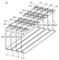
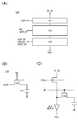
도 1은 본 발명의 일 형태에 따른 기억 장치의 구조예를 도시한 것이다. 도 1에 나타낸 기억 장치(10)는 센스 앰프(11), 및 센스 앰프(11)에 전기적으로 접속되는 메모리 셀(12a) 및 메모리 셀(12b)을 포함한다. 본 발명의 일 형태에서, 센스 앰프(11)는 제 1 층에 위치하고, 메모리 셀(12a 및 12b)은 제 1 층 위의 제 2 층에 위치한다.1 shows an example of the structure of a storage device according to an embodiment of the present invention. The
센스 앰프(11) 및 메모리 셀(12a 및 12b)이 하나의 층에 제공되는 경우에 비하여, 제 2 층에서의 메모리 셀(12a 및 12b)의 적어도 일부가 제 1 층에서의 센스 앰프(11)와 중첩되는 경우에는, 기억 장치(10)의 레이아웃 면적을 저감시킬 수 있고 단위 면적당 기억 용량을 증가시킬 수 있다.At least a portion of the
센스 앰프(11)는 기준 전위와, 메모리 셀(12a 또는 12b)로부터 출력되는 데이터-함유 신호의 전위의 전위차를 증폭하고, 증폭된 전위차를 유지한다. 구체적으로, 메모리 셀(12a)로부터 출력되는 데이터-함유 신호의 전위는 배선(BLa)을 통하여 센스 앰프(11)에 공급된다. 마찬가지로, 메모리 셀(12b)로부터 출력되는 데이터-함유 신호의 전위는 배선(BLb)을 통하여 센스 앰프(11)에 공급된다.The
메모리 셀(12a 및 12b) 각각은 스위칭 트랜지스터(13) 및 용량 소자(14)를 포함한다. 구체적으로, 메모리 셀(12a)의 트랜지스터(13)는, 트랜지스터(13)의 게이트에 접속된 배선(WLa)의 전위에 따라 온 상태 및 오프 상태가 된다. 또한, 용량 소자(14)는 트랜지스터(13)를 통하여 배선(BLa)에 전기적으로 접속된다. 마찬가지로, 메모리 셀(12b)의 트랜지스터(13)는, 트랜지스터(13)의 게이트에 접속된 배선(WLb)의 전위에 따라 온 상태 및 오프 상태가 된다. 또한, 용량 소자(14)는 트랜지스터(13)를 통하여 배선(BLb)에 전기적으로 접속된다.Each of the
도 1은 하나의 배선(BLa)이 하나의 메모리 셀(12a)에 전기적으로 접속되고, 하나의 배선(BLb)이 하나의 메모리 셀(12b)에 전기적으로 접속되는 예를 나타낸 것이다. 또한 본 발명의 일 형태의 기억 장치(10)에서는, 하나의 배선(BLa)이 복수의 메모리 셀(12a)에 전기적으로 접속되고, 하나의 배선(BLb)이 복수의 메모리 셀(12b)에 전기적으로 접속되어도 좋다.1 shows an example in which one wiring BLa is electrically connected to one
기억 장치(10)에 포함되는 메모리 셀(12a 및 12b)의 레이아웃에 관해서는, 접힘형(folded type) 또는 개방형(open type) 등을 사용할 수 있다. 접힘형의 경우, 배선(BLa 또는 BLb)으로부터 출력되는 데이터-함유 신호의 전위에 대한 배선(WLa 또는 WLb)의 전위 변화의 영향을 방지할 수 있다. 개방형의 경우, 메모리 셀(12a 및 12b)을 접힘형의 경우보다 높은 밀도로 레이아웃할 수 있어, 메모리 셀(12a 및 12b)을 포함하는 셀 어레이 전체를 작게 할 수 있다.As to the layout of the
도 1은 개방형 메모리 셀(12a 및 12b)을 포함하는 기억 장치(10)의 구조예를 나타낸 것이다. 구체적으로, 도 1에 나타낸 기억 장치(10)의 제 2 층에서, 배선(BLa)이 배선(WLa)과 교차하고 배선(WLb)과 교차하지 않고, 배선(BLb)이 배선(WLb)과 교차하고 배선(WLa)과 교차하지 않는다.1 shows an example of the structure of a
본 발명의 일 형태의 개방형에서는, 복수의 메모리 셀(12a) 및 복수의 메모리 셀(12b)이 형성되는 영역을 접힘형의 경우보다 작게 할 수 있다. 따라서, 제 1 층에 복수의 센스 앰프(11)를 가깝게 배치하더라도, 각 센스 앰프(11)에 대응하는 복수의 메모리 셀(12a 및 12b)을, 다른 메모리 셀의 영역으로 침입하는 일 없이 제 2 층에 배치할 수 있다. 본 발명의 일 형태는 개방형을 채용하기 때문에, 기억 장치(10)의 레이아웃 면적을 저감하고 단위 면적당 기억 용량을 증가시킬 수 있다.In the open type of one embodiment of the present invention, the area where the plurality of
또한, 메모리 셀(12a 및 12b) 및 센스 앰프(11)가 적층되기 때문에, 메모리 셀(12a 및 12b)을 센스 앰프(11)에 전기적으로 접속시키는 배선(배선(BLa), 배선(BLb) 등)의 길이를 줄일 수 있다. 배선의 저항을 작게 할 수 있어, 기억 장치(10)에서 소비 전력의 저감 및 고속 동작을 실현할 수 있다.Since the
또한 메모리 셀(12a 및 12b)은 하나의 센스 앰프(11)와 중첩되어도 좋고, 각각 상이한 센스 앰프(11)와 중첩되어도 좋다.The
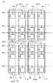
도 2는 하나의 센스 앰프(11)에 전기적으로 접속되는 메모리 셀(12a 및 12b)이 상기 센스 앰프(11)와 중첩되는 개방형 기억 장치(10)의 구조예를 나타낸 것이다. 도 3은 도 2에서의 기억 장치(10)의 상면도이다.2 shows an example of the structure of an open
도 2 및 도 3의 기억 장치(10)는, 제 1 층에서의 하나의 센스 앰프(11)와 상기 센스 앰프(11)에 전기적으로 접속되는 복수의 메모리 셀(12a) 및 복수의 메모리 셀(12b)을 4개 세트 포함한다. 도 2 및 도 3에서 4개의 센스 앰프(11)를 센스 앰프(11-1, 11-2, 11-3, 및 11-4)로 나타낸다. 본 발명의 일 형태의 기억 장치(10)에 포함되는 세트의 수는 하나, 2개, 3개이어도 좋고, 4개보다 많아도 좋다.The
도 2 및 도 3에서는, 복수의 메모리 셀(12a)을 포함하는 영역(15a) 및 복수의 메모리 셀(12b)을 포함하는 영역(15b)이, 복수의 메모리 셀(12a 및 12b)에 전기적으로 접속되는 센스 앰프(11)와 중첩된다.2 and 3, a
또한 도 2 및 도 3에서는, 센스 앰프(11-1, 11-2, 11-3, 및 11-4)가 각각 배선(BLa1, BLa2, BLa3, 및 BLa4)에 전기적으로 접속되고, 각각 배선(BLb1, BLb2, BLb3, 및 BLb4)에 전기적으로 접속된다. 영역(15a)의 복수의 메모리 셀(12a)은 BLa1~BLa4로 나타내는 하나의 배선(BLa)에 전기적으로 접속된다. 영역(15b)의 복수의 메모리 셀(12b)은 BLb1~BLb4로 나타내는 배선(BLb) 중 하나에 전기적으로 접속된다.2 and 3, the sense amplifiers 11-1, 11-2, 11-3, and 11-4 are electrically connected to the wirings BLa1, BLa2, BLa3, and BLa4, respectively, BLb1, BLb2, BLb3, and BLb4. A plurality of
각각 상이한 센스 앰프(11-1~11-4)에 전기적으로 접속되는 메모리 셀(12a)을 포함하는 4개의 영역(15a)은 복수의 배선(WLa)을 공유한다. 구체적으로, 하나의 배선(WLa)은 각각 상이한 배선(BLa1~BLa4)에 전기적으로 접속되는 각 영역(15a)에서의 4개의 메모리 셀(12a)에 전기적으로 접속된다. 마찬가지로, 각각 상이한 센스 앰프(11-1~11-4)에 전기적으로 접속되는 메모리 셀(12b)을 포함하는 4개의 영역(15b)은 복수의 배선(WLb)을 공유한다. 구체적으로, 하나의 배선(WLb)은 각각 상이한 배선(BLb1~BLb4)에 전기적으로 접속되는 4개의 메모리 셀(12b)에 전기적으로 접속된다.The four
도 2 및 도 3에 나타낸 개방형 기억 장치(10)에서는, 각 배선(BLa)이 제 2 층에서 배선(WLa)과 교차하고 배선(WLb)과는 교차하지 않는다. 마찬가지로, 각 배선(BLb)이 제 2 층에서 배선(WLb)과 교차하고 배선(WLa)과는 교차하지 않는다.In the open-
이 구조에 의하여, 도 2 및 도 3에 나타낸 기억 장치(10)의 레이아웃 면적을 저감할 수 있고 단위 면적당 기억 용량을 증가시킬 수 있다.With this structure, the layout area of the
도 4는 개방형 기억 장치(10)의 구조예를 나타낸 것이다. 이 기억 장치(10)에서는, 메모리 셀(12a)이 상이한 2개의 센스 앰프(11)에 전기적으로 접속되고 이들 센스 앰프(11) 중 하나와 중첩되고, 메모리 셀(12b)이 상기 2개의 센스 앰프(11)에 전기적으로 접속되고 이들 센스 앰프(11) 중 다른 하나와 중첩된다. 도 5는 도 4에 나타낸 기억 장치(10)의 상면도이다.Fig. 4 shows an example of the structure of the open
도 4 및 도 5의 기억 장치(10)는, 제 1 층에서의 하나의 센스 앰프(11)와 센스 앰프(11)에 전기적으로 접속되는 복수의 메모리 셀(12a) 및 복수의 메모리 셀(12b)을 4개 세트 포함한다. 도 4 및 도 5에서도 4개의 센스 앰프(11)를 센스 앰프(11-1, 11-2, 11-3, 및 11-4)로 나타낸다. 본 발명의 일 형태의 기억 장치(10)의 세트의 수는 2개, 3개이어도 좋고, 4개보다 많아도 좋다.4 and 5 includes a plurality of
도 4 및 도 5에서, 센스 앰프(11-1)에 전기적으로 접속되는 메모리 셀(12a) 및 센스 앰프(11-2)에 전기적으로 접속되는 메모리 셀(12a)이 센스 앰프(11-1)와 중첩된다. 센스 앰프(11-1)에 전기적으로 접속되는 메모리 셀(12b) 및 센스 앰프(11-2)에 전기적으로 접속되는 메모리 셀(12b)이 센스 앰프(11-2)와 중첩된다. 센스 앰프(11-3)에 전기적으로 접속되는 메모리 셀(12a) 및 센스 앰프(11-4)에 전기적으로 접속되는 메모리 셀(12a)이 센스 앰프(11-3)와 중첩된다. 센스 앰프(11-3)에 전기적으로 접속되는 메모리 셀(12b) 및 센스 앰프(11-4)에 전기적으로 접속되는 메모리 셀(12b)이 센스 앰프(11-4)와 중첩된다.4 and 5, the
또한 도 4 및 도 5에서는, 센스 앰프(11-1~11-4)가 각각 배선(BLa1~BLa4)에 전기적으로 접속되고, 각각 BLb1~BLb4에 전기적으로 접속된다. 하나의 영역(15a)의 복수의 메모리 셀(12a)은 BLa1~BLa4로 나타내는 하나의 배선(BLa)에 전기적으로 접속된다. 하나의 영역(15b)의 복수의 메모리 셀(12b)은 BLb1~BLb4로 나타내는 하나의 배선(BLb)에 전기적으로 접속된다.4 and 5, the sense amplifiers 11-1 to 11-4 are electrically connected to the wirings BLa1 to BLa4, respectively, and are electrically connected to BLb1 to BLb4, respectively. A plurality of
도 4 및 도 5의 기억 장치(10)에서, 각각 상이한 센스 앰프(11-1~11-4)에 전기적으로 접속되는 메모리 셀(12a)을 포함하는 4개의 영역(15a)이 복수의 배선(WLa)을 공유한다. 각각 상이한 센스 앰프(11-1~11-4)에 전기적으로 접속되는 메모리 셀(12b)을 포함하는 4개의 영역(15b)이 복수의 배선(WLb)을 공유한다.4 and 5, four
구체적으로, 각각 상이한 센스 앰프(11-1~11-4)에 전기적으로 접속되는 메모리 셀(12a)을 포함하는 4개의 영역(15a)에서, 하나의 배선(WLa)은, 각각 상이한 배선(BLa1~BLa4)에 전기적으로 접속되는 4개의 메모리 셀(12a)에 전기적으로 접속된다. 각각 상이한 센스 앰프(11-1~11-4)에 전기적으로 접속되는 메모리 셀(12b)을 포함하는 4개의 영역(15b)에서, 하나의 배선(WLb)은, 각각 상이한 배선(BLb1~BLb4)에 전기적으로 접속되는 4개의 메모리 셀(12b)에 전기적으로 접속된다.Specifically, in the four
도 4 및 도 5에 나타낸 개방형 기억 장치(10)에서는, 임의의 배선(BLa)이 제 2 층에서 배선(WLa)과 교차하고 배선(WLb)과는 교차하지 않는다. 마찬가지로, 하나의 배선(BLb)이 제 2 층에서 배선(WLb)과 교차하고 배선(WLa)과는 교차하지 않는다.In the
이 구조에 의하여, 도 4 및 도 5에 나타낸 기억 장치(10)의 레이아웃 면적을 저감할 수 있고 단위 면적당 기억 용량을 증가시킬 수 있다.With this structure, the layout area of the
<기억 장치의 구체적인 구조예><Example of specific structure of memory device>
다음에, 본 발명의 일 형태에 따른 기억 장치(10)의 구체적인 구조예에 대하여 설명한다.Next, a specific structural example of the
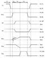
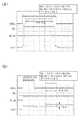
도 6은 메모리 셀(12a 및 12b), 메모리 셀(12a 및 12b)에 전기적으로 접속되는 센스 앰프(11), 프라차지 회로(20), 스위치 회로(21), 및 메인 앰프(23)의 접속의 예를 나타낸 것이다.Fig. 6 is a circuit diagram showing the connection of the
프리차지 회로(20)는 배선(BLa 및 BLb)의 전위를 초기화하는 기능을 갖는다. 스위치 회로(21)는 배선(BLa 및 BLb)과 메인 앰프(23)의 도통 상태를 전환하는 기능을 갖는다. 본 실시형태에서는, 센스 앰프(11)에 더하여, 프리차지 회로(20) 또는 스위치 회로(21)를 메모리 셀(12a 및 12b)과 중첩되도록 제 1 층에 제공할 수도 있다. 이하에서, 센스 앰프(11), 프리차지 회로(20), 및 스위치 회로(21)를 집합적으로 구동 회로(22)라고 한다.The
메모리 셀(12a)은 배선(BLa)을 통하여 구동 회로(22)에 전기적으로 접속된다. 메모리 셀(12b)은 배선(BLb)을 통하여 구동 회로(22)에 전기적으로 접속된다.The
도 6에서는 하나의 메모리 셀(12a)이 하나의 배선(BLa)을 통하여 구동 회로(22)에 전기적으로 접속되지만, 복수의 메모리 셀(12a)이 하나의 배선(BLa)을 통하여 구동 회로(22)에 전기적으로 접속되어도 좋다. 도 6에서는 하나의 메모리 셀(12b)이 하나의 배선(BLb)을 통하여 구동 회로(22)에 전기적으로 접속되지만, 복수의 메모리 셀(12b)이 하나의 배선(BLb)을 통하여 구동 회로(22)에 전기적으로 접속되어도 좋다. 또한 같은 배선(BLa)에 접속되는 메모리 셀(12a)은 각각 상이한 배선(WLa)에 전기적으로 접속되고, 같은 배선(BLb)에 접속되는 메모리 셀(12b)은 각각 상이한 배선(WLb)에 전기적으로 접속된다.6, one
도 6에서의 센스 앰프(11)는 래치형 센스 앰프이다. 구체적으로, 도 6의 센스 앰프(11)는 p채널형 트랜지스터(30 및 31) 및 n채널형 트랜지스터(32 및 33)를 포함한다. 트랜지스터(30)의 소스 및 드레인 중 한쪽은 배선(SP)에 전기적으로 접속되고, 다른 쪽은 트랜지스터(31 및 33)의 게이트 및 배선(BLa)에 전기적으로 접속된다. 트랜지스터(32)의 소스 및 드레인 중 한쪽은 트랜지스터(31 및 33)의 게이트 및 배선(BLa)에 전기적으로 접속되고, 다른 쪽은 배선(SN)에 전기적으로 접속된다. 트랜지스터(31)의 소스 및 드레인 중 한쪽은 배선(SP)에 전기적으로 접속되고, 다른 쪽은 트랜지스터(30 및 32)의 게이트 및 배선(BLb)에 전기적으로 접속된다. 트랜지스터(33)의 소스 및 드레인 중 한쪽은 트랜지스터(30 및 32)의 게이트 및 배선(BLb)에 전기적으로 접속되고, 다른 쪽은 배선(SN)에 전기적으로 접속된다.The
프리차지 회로(20)는 n채널형 트랜지스터(34~36)를 포함한다. 트랜지스터(34~36)는 p채널형 트랜지스터이어도 좋다. 트랜지스터(34)의 소스 및 드레인 중 한쪽은 배선(BLa)에 전기적으로 접속되고, 다른 쪽은 배선(Pre)에 전기적으로 접속된다. 트랜지스터(35)의 소스 및 드레인 중 한쪽은 배선(BLb)에 전기적으로 접속되고, 다른 쪽은 배선(Pre)에 전기적으로 접속된다. 트랜지스터(36)의 소스 및 드레인 중 한쪽은 배선(BLa)에 전기적으로 접속되고, 다른 쪽은 배선(BLb)에 전기적으로 접속된다. 트랜지스터(34~36)의 게이트는 배선(PL)에 전기적으로 접속된다.The
스위치 회로(21)는 n채널형 트랜지스터(37 및 38)를 포함한다. 트랜지스터(37 및 38)는 p채널형 트랜지스터이어도 좋다. 트랜지스터(37)의 소스 및 드레인 중 한쪽은 배선(BLa)에 전기적으로 접속되고, 다른 쪽은 배선(IOa)에 전기적으로 접속된다. 트랜지스터(38)의 소스 및 드레인 중 한쪽은 배선(BLb)에 전기적으로 접속되고, 다른 쪽은 배선(IOb)에 전기적으로 접속된다. 트랜지스터(37 및 38)의 게이트는 배선(CSL)에 전기적으로 접속된다.The
배선(IOa 및 IOb)은 메인 앰프(23)에 전기적으로 접속된다.The wirings IOa and IOb are electrically connected to the
다음에, 도 6에 나타낸 메모리 셀(12a 및 12b), 구동 회로(22), 및 메인 앰프(23)의 데이터 판독의 동작예에 대하여 도 7의 타이밍 차트를 참조하여 설명한다.Next, an operation example of data reading of the
우선, 기간(T1)에서, 프리차지 회로(20)에 포함되는 트랜지스터(34~36)를 온 상태로 하여 배선(BLa 및 BLb)의 전위를 초기화한다. 구체적으로, 도 7에서, 배선(PL)에 하이 레벨 전위(VH_PL)를 공급하여 프리차지 회로(20)에서 트랜지스터(34~36)를 온 상태로 한다. 이런 방식으로, 배선(Pre)의 전위(Vpre)가 배선(BLa 및 BLb)에 공급된다.First, in the period T1, the
또한 기간(T1)에서는, 배선(CSL)에 로 레벨 전위(VL_CSL)가 공급되기 때문에, 스위치 회로(21)에서 트랜지스터(37 및 38)는 오프 상태이다. 배선(WLa)에는 로 레벨 전위(VL_WL)가 공급되기 때문에, 메모리 셀(12a)에서 트랜지스터(13)는 오프 상태이다. 배선(WLb)에도 로 레벨 전위(VL_WL)가 공급되기 때문에, 메모리 셀(12b)에서 트랜지스터(13)는 오프 상태이다(도 7에는 나타내지 않았음). 배선(SP 및 SN)에는 전위(Vpre)가 공급되기 때문에, 센스 앰프(11)는 오프 상태이다.In the period T1, since the low level potential VL_CSL is supplied to the wiring CSL, the
그리고, 배선(PL)에 로 레벨 전위(VL_PL)를 공급하여 프리차지 회로(20)에서 트랜지스터(34~36)를 오프 상태로 한다. 기간(T2)에서, 배선(WLa)이 선택된다. 구체적으로, 도 7에서, 배선(WLa)에 하이 레벨 전위(VH_WL)를 공급하여 배선(WLa)을 선택하고 메모리 셀(12a)에서 트랜지스터(13)를 온 상태로 한다. 이로써 배선(BLa) 및 용량 소자(14)는 트랜지스터(13)를 통하여 서로 전기적으로 접속된다. 배선(BLa) 및 용량 소자(14)가 서로 전기적으로 접속되기 때문에, 용량 소자(14)에 유지된 전하량에 따라 배선(BLa)의 전위가 변화한다.Then, a low level potential VL_PL is supplied to the wiring line PL to turn off the
도 7의 타이밍 차트는, 용량 소자(14)에 축적된 전하량이 큰 경우를 예로서 나타낸다. 구체적으로, 용량 소자(14)에 축적된 전하량이 큰 경우에는 용량 소자(14)로부터 배선(BLa)에 전하가 방출되어, 배선(BLa)의 전위가 전위(Vpre)로부터 ΔV1만큼 상승된다. 용량 소자(14)에 축적된 전하량이 작은 경우에는, 배선(BLa)으로부터 용량 소자(14)에 전하가 흘러, 배선(BLa)의 전위가 ΔV2만큼 저하된다.The timing chart of Fig. 7 shows an example in which the amount of charge accumulated in the
또한 기간(T2)에서, 배선(CSL)에는 로 레벨 전위(VL_CSL)가 계속 공급되고 있기 때문에, 스위치 회로(21)에서 트랜지스터(37 및 38)는 오프 상태를 유지한다. 배선(SP 및 SN)에는 전위(Vpre)가 계속 공급되고 있기 때문에, 센스 앰프(11)는 오프 상태를 유지한다.Since the low level potential VL_CSL is continuously supplied to the wiring CSL in the period T2, the
기간(T3)에서, 배선(SP)에 하이 레벨 전위(VH_SP)를 공급하고 배선(SN)에 로 레벨 전위(VL_SN)를 공급하여, 센스 앰프(11)를 온 상태로 한다. 센스 앰프(11)는 배선(BLa와 BLb)의 전위차(도 7에서는 ΔV1)를 증폭하는 기능을 갖는다. 따라서, 도 7의 타이밍 차트에서, 센스 앰프(11)를 온 상태로 함으로써, 배선(BLa)의 전위는 전위(Vpre+ΔV1)로부터 상승되어 배선(SP)의 전위(VH_SP)에 가까워진다. 배선(BLb)의 전위는 전위(Vpre)로부터 저하되어 배선(SN)의 전위(VL_SN)에 가까워진다.During the period T3, the high level potential VH_SP is supplied to the wiring SP and the low level potential VL_SN is supplied to the wiring SN to turn the
또한 기간(T3)의 초기에 배선(BLa)의 전위가 Vpre-ΔV2인 경우에는, 센스 앰프(11)가 온 상태가 됨으로써, 배선(BLa)의 전위가 전위(Vpre-ΔV2)로부터 저하되어 배선(SN)의 전위(VL_SN)에 가까워진다. 배선(BLb)의 전위는 전위(Vpre)로부터 상승되어 배선(SP)의 전위(VH_SP)에 가까워진다.When the potential of the wiring BLa is Vpre -? V2 at the beginning of the period T3, the potential of the wiring BLa is lowered from the potential Vpre -? V2 by turning on the
기간(T3)에서는, 배선(PL)에 로 레벨 전위(VL_PL)가 계속 공급되고 있어 프리차지 회로(20)에서 트랜지스터(34~36)는 오프 상태를 유지한다. 배선(CSL)에는 로 레벨 전위(VL_CSL)가 계속 공급되고 있어, 스위치 회로(21)에서 트랜지스터(37 및 38)는 오프 상태를 유지한다. 배선(WLa)에는 하이 레벨 전위(VH_WL)가 계속 공급되고 있어, 메모리 셀(12a)에서 트랜지스터(13)는 온 상태를 유지한다. 그 결과, 배선(BLa)의 전위(VH_SP)에 따른 전하가 메모리 셀(12a)에서의 용량 소자(14)에 축적된다.During the period T3, the low level potential VL_PL is continuously supplied to the wiring PL, and the
다음에, 기간(T4)에서, 배선(CSL)에 공급되는 전위를 변화시켜 스위치 회로(21)를 온 상태로 한다. 구체적으로, 도 7에서, 배선(CSL)에 하이 레벨 전위(VH_CSL)를 공급하여, 스위치 회로(21)에서 트랜지스터(37 및 38)를 온 상태로 한다. 이 방식으로, 배선(BLa)의 전위 및 배선(BLb)의 전위가 배선(IOa 및 IOb)을 통하여 메인 앰프(23)에 공급된다. 메인 앰프(23)로부터 출력되는 전위(Vout)의 레벨은, 배선(IOa)의 전위가 배선(IOb)의 전위보다 높은지 여부에 의존한다. 이 이유로, 전위(Vout)를 포함하는 신호는 메모리 셀(12a)로부터 판독되는 데이터를 반영한다.Next, in the period T4, the potential supplied to the wiring CSL is changed so that the
또한 기간(T4)에서는, 배선(PL)에 로 레벨 전위(VL_PL)가 계속 공급되고 있어, 프리차지 회로(20)에서 트랜지스터(34 및 36)는 오프 상태를 유지한다. 또한, 배선(WLa)에는 하이 레벨 전위(VH_WL)가 계속 공급되고 있어, 메모리 셀(12a)에서 트랜지스터(13)는 온 상태를 유지한다. 배선(SP)에 하이 레벨 전위(VH_SP)가 계속 공급되고 있고 배선(SN)에 로 레벨 전위(VL_SN)가 계속 공급되고 있기 때문에, 센스 앰프(11)는 온 상태를 유지한다. 그 결과, 배선(BLa)의 전위(VH_SP)에 대응하는 전하가 메모리 셀(12a)의 용량 소자(14)에 축적된다.Further, during the period T4, the low level potential VL_PL is continuously supplied to the wiring line PL, and the
기간(T4)이 끝나면, 배선(CSL)에 공급되는 전위를 변화시켜 스위치 회로(21)를 오프 상태로 한다. 구체적으로, 도 7에서, 배선(CSL)에 로 레벨 전위(VL_CSL)를 공급하여 스위치 회로(21)에서 트랜지스터(37 및 38)를 오프 상태로 한다.At the end of the period T4, the potential supplied to the wiring CSL is changed so that the
또한 기간(T4)이 끝나면 배선(WLa)을 비선택으로 한다. 구체적으로, 도 7에서, 배선(WLa)에 로 전위(VL_WL)를 공급함으로써, 배선(WLa)을 비선택으로 하여 메모리 셀(12a)에서 트랜지스터(13)를 오프 상태로 한다. 이 동작을 거쳐, 배선(BLa)의 전위(VH_SP)에 대응하는 전하가 용량 소자(14)에 유지되기 때문에, 데이터 판독 후에도 메모리 셀(12a)에 데이터가 유지된다.When the period T4 ends, the wiring WLa is made non-selected. Specifically, in FIG. 7, the potential VL_WL is supplied to the wiring line WLa, thereby making the wiring line WLa non-selected and turning off the
기간(T1~T4)의 동작을 거쳐, 메모리 셀(12a)로부터 데이터가 판독된다. 메모리 셀(12b)의 데이터도 마찬가지로 판독될 수 있다.Data is read from the
또한 데이터 판독과 같은 동작에 의하여 다른 데이터를 메모리 셀(12a 또는 12b)에 기록할 수 있다. 우선, 프리차지 회로(20)에 포함되는 트랜지스터(34~36)를 온 상태로 하여 배선(BLa 및 BLb)의 전위를 초기화한다. 그리고, 데이터가 기록되는 메모리 셀(12a)에 전기적으로 접속되는 배선(WLa) 또는 데이터가 기록되는 메모리 셀(12b)에 전기적으로 접속되는 배선(WLb)을 선택하여 메모리 셀(12a 또는 12b)에서 트랜지스터(13)를 온 상태로 한다. 이로써, 배선(BLa 또는 BLb)과 용량 소자(14)가 트랜지스터(13)를 통하여 서로 전기적으로 접속된다. 그 후, 배선(SP)에 하이 레벨 전위(VH_SP)를 공급하고 배선(SN)에 로 레벨 전위(VL_SN)를 공급함으로써, 센스 앰프(11)를 온 상태로 한다. 그러고 나서, 배선(CSL)에 공급되는 전위를 변화시켜 스위치 회로(21)를 온 상태로 한다. 구체적으로, 배선(CSL)에 하이 레벨 전위(VH_CSL)를 공급하여, 스위치 회로(21)에서 트랜지스터(37 및 38)를 온 상태로 한다. 결과적으로, 배선들(BLa 및 IOa)이 서로 전기적으로 접속되고, 배선들(BLb 및 IOb)이 서로 전기적으로 접속된다. 기록하는 데이터에 대응하는 전위를 배선(IOa 및 IOb)에 공급함으로써, 기록하는 데이터에 대응하는 전위를 스위치 회로(21)를 통하여 배선(BLa 및 BLb)에 공급한다. 이 동작에 의하여, 배선(BLa 또는 BLb)의 전위에 따라 용량 소자(14)에 전하가 축적되므로, 메모리 셀(12a 또는 12b)에 데이터가 기록된다.Further, other data can be written to the
또한 배선(BLa)에 배선(IOa)의 전위가 공급되고 배선(BLb)에 배선(IOb)의 전위가 공급된 후에는, 스위치 회로(21)에서 트랜지스터(37 및 38)를 오프 상태로 하고 나서도 센스 앰프(11)가 오프 상태이기만 하면, 배선(BLa)의 전위와 배선(BLb)의 전위 사이의 레벨의 관계는 센스 앰프(11)에 의하여 유지된다. 따라서, 스위치 회로(21)에서 트랜지스터(37 및 38)를 온 상태로 하는 타이밍은 배선(WLa)의 선택 전이어도 선택 후이어도 좋다.After the potential of the wiring Ioa is supplied to the wiring BLa and the potential of the wiring Iob is supplied to the wiring BLb, the
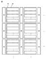
도 8은 메모리 셀(12a 및 12b)을 각각 포함하는 셀 어레이(41), 구동 회로(22), 및 배선(WLa 및 WLb)의 전위를 제어하는 행 디코더(42)를 포함하는 어레이(40)의 레이아웃의 예를 나타낸 것이다. 어레이(40)는 본 발명의 일 형태의 기억 장치의 일 형태이다.8 shows an
도 8의 어레이(40)에서는, 제 1 층에서의 구동 회로(22)가 제 2 층에서의 셀 어레이(41)와 중첩된다. 셀 어레이(41)에 포함되는 메모리 셀(12a 및 12b)의 개수 및 구동 회로(22)의 개수는 설계자가 결정할 수 있다.In the
행 디코더(42)는 제 1 층 또는 제 2 층에 위치하고, 인접한 셀 어레이(41)에 포함되는 메모리 셀(12a 및 12b)에 전기적으로 접속되는 배선(WLa 및 WLb)의 전위를 제어한다.The
도 9는 도 8에 나타낸 어레이(40), 및 어레이(40)의 동작을 제어하는 구동 회로(43)를 포함하는 기억 장치(44)의 구조예를 나타낸 것이다. 기억 장치(44)는 본 발명의 일 형태의 기억 장치의 일 형태이다.Fig. 9 shows an example of the structure of the
구체적으로, 도 9의 기억 장치(44)의 구동 회로(43)는 버퍼(45), 메인 앰프(23), 열 디코더(46), 기록 회로(47), 및 행 디코더(48)를 포함한다.9 includes a
버퍼(45)는, 구동 회로(43) 또는 어레이(40)를 구동하기 위하여 사용되는 신호, 및 어레이(40)에 기록되는 데이터의, 기억 장치(44)에 대한 입력을 제어한다. 또한 버퍼(45)는 어레이(40)로부터 판독되는 데이터의, 기억 장치(44)로부터의 출력을 제어한다.The
행 디코더(48)는 도 8의 어레이(40)에 포함되는 복수의 행 디코더(42)로부터 지정된 어드레스에 기초하여 행 디코더(42)를 선택한다. 선택된 행 디코더(42)는 도 6에 나타낸 배선(WLa 또는 WLb)을 선택한다.The
열 디코더(46)는 스위치 회로(21)의 동작을 제어하여, 데이터 기록 또는 판독 시에 지정된 어드레스에 따라 열 방향의 메모리 셀(12a 및 12b)을 선택하는 기능을 갖는다. 구체적으로, 도 6의 기억 장치(10)의 열 디코더(46)는 배선(CSL)의 전위를 제어하는 기능을 갖는다.The
스위치 회로(21)는 배선(BLa 및 BLb)과 메인 앰프(23)의 도통 상태, 및 배선(BLa 및 BLb)과 기록 회로(47)의 도통 상태를 전환하는 기능을 갖는다. 기록 회로(47)는 지정된 어드레스의 메모리 셀(12a 또는 12b)에 스위치 회로(21)를 통하여 데이터를 기록하는 기능을 갖는다. 구체적으로, 도 6에 나타낸 기억 장치(10)의 기록 회로(47)는 데이터에 따라 배선(IOa 및 IOb)에 전위를 공급하는 기능을 갖는다.The
메인 앰프(23)는, 센스 앰프(11)에 의하여 증폭된 배선(BLa 및 BLb)의 전위를 사용하여, 데이터를 판독하는 기능을 갖는다.The
또한 기억 장치(44)는, 지정된 메모리 셀(12a 또는 12b)의 어드레스를 임시적으로 저장할 수 있는 어드레스 버퍼를 포함하여도 좋다.The
<기억 장치의 단면 구조의 예 1>≪ Example 1 of sectional structure of memory device >
도 10은 본 발명의 일 형태에 따른 기억 장치의 단면 구조의 예를 도시한 것이다. 또한 도 10은 도 6에 나타낸 기억 장치(10)에 포함되는 트랜지스터(13), 용량 소자(14), 및 트랜지스터(30)의 단면도이다. 기억 장치의 단면 구조를 도시한 도 10에서, 단결정 기판에 채널 형성 영역을 포함하는 트랜지스터(30)가 제 1 층에 위치하고, 용량 소자(14) 및 산화물 반도체막에 채널 형성 영역을 포함하는 트랜지스터(13)가 제 1층 위의 제 2 층에 위치한다.10 shows an example of a cross-sectional structure of a storage device according to an embodiment of the present invention. 10 is a cross-sectional view of the
트랜지스터(30)는 비정질, 미결정, 다결정, 또는 단결정 상태의 실리콘 또는 저마늄 등의 반도체막 또는 반도체 기판에 채널 형성 영역을 포함하여도 좋다. 실리콘 박막을 사용하여 트랜지스터(30)를 형성하는 경우, 그 박막에는, PECVD(Plasma-Enhanced Chemical Vapor Deposition)법 등의 기상 성장법 또는 스퍼터링법에 의하여 형성되는 비정질 실리콘; 레이저 어닐링 등의 처리에 의한 비정질 실리콘의 결정화로 얻어지는 다결정 실리콘; 및 단결정 실리콘 웨이퍼에 수소 이온 등을 주입함으로써 이 실리콘 웨이퍼의 표면 부분을 분리시켜 얻어지는 단결정 실리콘 등을 사용할 수 있다.The
트랜지스터(30)가 형성되는 반도체 기판(601)은 예를 들어, 실리콘 기판, 저마늄 기판, 또는 실리콘 저마늄 기판일 수 있다. 도 10에서는 반도체 기판(601)으로서 단결정 실리콘 기판이 사용된다.The
트랜지스터(30)는 소자 분리법에 의하여 전기적으로 분리된다. 소자 분리법으로서는, 선택 산화법(LOCOS법: local oxidation of silicon method), 트렌치 분리법(STI법: shallow trench isolation method) 등을 사용할 수 있다. 도 10은 트랜지스터(30)를 전기적으로 분리시키기 위하여 트렌치 분리법을 사용한 예를 도시한 것이다. 구체적으로, 도 10에서는, 에칭 등에 의하여 반도체 기판(601)에 형성된 트렌치에 산화 실리콘 등을 포함하는 절연체를 매립하여 소자 분리 영역(610)을 형성함으로써, 트랜지스터(30)를 소자 분리에 의하여 전기적으로 분리시킨다.The
트랜지스터(30) 위에 절연막(611)이 제공된다. 절연막(611)에는 개구가 형성된다. 개구에는, 트랜지스터(30)의 소스 및 드레인에 전기적으로 접속되는 도전막(625 및 626)이 형성된다.An insulating
도전막(625)은 절연막(611) 위에 형성되는 도전막(634)에 전기적으로 접속된다. 도전막(626)은 절연막(611) 위에 형성되는 도전막(635)에 전기적으로 접속된다.The
도전막(634~636) 위에 절연막(612)이 형성된다. 절연막(612)에는 개구가 형성된다. 개구에는, 도전막(636)에 전기적으로 접속되는 도전막(637)이 형성된다. 도전막(637)은 절연막(612) 위에 형성되는 도전막(651)에 전기적으로 접속된다.An insulating
도전막(651) 위에 절연막(613)이 형성된다. 절연막(613)에는 개구가 형성된다. 개구에는, 도전막(651)에 전기적으로 접속되는 도전막(652)이 형성된다. 도전막(652)은 절연막(613) 위에 형성되는 도전막(653)에 전기적으로 접속된다. 절연막(613) 위에는 도전막(644)이 형성된다.An insulating
도전막(653) 및 도전막(644) 위에 절연막(661)이 형성된다. 도 10에서는, 절연막(661) 위에 트랜지스터(13) 및 용량 소자(14)가 형성된다.An insulating
트랜지스터(13)는, 절연막(661) 위에, 산화물 반도체를 포함하는 반도체막(701), 반도체막(701) 위의 소스 및 드레인으로서 기능하는 도전막(721 및 722), 반도체막(701) 및 도전막(721 및 722) 위의 게이트 절연막(662), 및 게이트 절연막(662) 위에 있으며 도전막들(721 및 722) 사이에서 반도체막(701)과 중첩되는 게이트 전극(731)을 포함한다. 또한 도전막(721 및 722)은 절연막(661)에 형성된 개구에서 도전막(644 및 653)에 각각 전기적으로 접속된다.The
트랜지스터(13)의 반도체막(701)에서는, 도전막(721)과 중첩되는 영역과 게이트 전극(731)과 중첩되는 영역 사이에 영역(710)이 있다. 또한, 트랜지스터(13)의 반도체막(701)에서는, 도전막(722)과 중첩되는 영역과 게이트 전극(731)과 중첩되는 영역 사이에 영역(711)이 있다. 아르곤, p형 도전성을 반도체막(701)에 부여하는 불순물, 또는 n형 도전성을 반도체막(701)에 부여하는 불순물을, 도전막(721 및 722) 및 게이트 전극(731)을 마스크로서 사용하여 영역(710 및 711)에 첨가하면, 반도체막(701)에서 영역(710 및 711)의 저항을 게이트 전극(731)과 중첩되는 영역보다 낮게 할 수 있다.The
용량 소자(14)는, 절연막(661) 위의 도전막(722), 도전막(722)과 중첩되는 게이트 절연막(662), 및 게이트 절연막(662)을 개재(介在)하여 도전막(722)과 중첩되는 도전막(655)을 포함한다. 게이트 절연막(662) 위에 도전막을 형성하고 이 도전막을 원하는 형상으로 가공함으로써, 게이트 전극(731)과 함께 도전막(655)을 형성할 수 있다.The
트랜지스터(13) 및 용량 소자(14) 위에 절연막(663)이 제공된다.An insulating
도 10에 나타낸 기억 장치에서, 트랜지스터(13)의 소스 전극 또는 드레인 전극으로서 기능하는 도전막(722)과 트랜지스터(30)의 소스 전극 또는 드레인 전극으로서 기능하는 도전막(652)을 전기적으로 접속시키는 도전막(634, 637, 651, 및 653)은 배선(BLa)에 상당한다. 이들 도전막에 더하여, 도전막(722)의 일부 또는 도전막(625)의 일부가 배선(BLa)에 포함되어도 좋다.A
도 10에서 트랜지스터(13)는 반도체막(701)의 적어도 한 측에 게이트 전극(731)을 갖지만, 트랜지스터(13)는 반도체막(701)을 개재한 한 쌍의 게이트 전극을 가져도 좋다.The
트랜지스터(13)가 반도체막(701)을 개재한 한 쌍의 게이트 전극을 갖는 경우, 게이트 전극들 중 한쪽은 온/오프 상태를 제어하기 위한 신호를 공급받을 수 있고, 게이트 전극들 중 다른 쪽은 다른 배선으로부터 전위를 공급받을 수 있다. 이 경우, 한 쌍의 게이트 전극에 같은 레벨의 전위가 공급되어도 좋고, 또는 게이트 전극들 중 다른 쪽에만 접지 전위 등의 고정 전위가 공급되어도 좋다. 게이트 전극들 중 다른 쪽에 공급되는 전위의 레벨을 제어함으로써, 트랜지스터의 문턱 전압을 제어할 수 있다.When the
도 10에서 트랜지스터(13)는 하나의 게이트 전극(731)에 대응하는 하나의 채널 형성 영역을 포함하는 싱글 게이트 구조를 갖는다. 그러나, 트랜지스터(13)는 서로 전기적으로 접속된 복수의 게이트 전극이 제공되어 하나의 활성층에 복수의 채널 형성 영역이 포함되는 멀티 게이트 구조를 가져도 좋다.In FIG. 10, the
<트랜지스터>≪ Transistor &
다음에, 산화물 반도체막에 채널 형성 영역이 형성된 트랜지스터(90)의 구조예에 대하여 설명한다.Next, an example of the structure of the
도 11의 (A)~(C)는 일례로서 산화물 반도체막에 채널 형성 영역을 포함하는 트랜지스터(90)의 구조를 도시한 것이다. 도 11의 (A)는 트랜지스터(90)의 상면도이다. 또한, 트랜지스터(90)의 레이아웃을 명확하게 하기 위하여 도 11의 (A)에는 절연막을 도시하지 않았다. 도 11의 (B)는 도 11의 (A)의 상면도에서의 일점쇄선 A1-A2를 따르는 단면도이다. 도 11의 (C)는 도 11의 (A)의 상면도에서의 일점쇄선 A3-A4를 따르는 단면도이다.11A to 11C illustrate the structure of a
도 11의 (A)~(C)에 도시된 바와 같이, 트랜지스터(90)는 기판(97) 위에 형성된 절연막(91) 위에 순차적으로 적층된 산화물 반도체막(92a) 및 산화물 반도체막(92b); 산화물 반도체막(92b)에 전기적으로 접속되며 소스 전극 및 드레인 전극으로서 기능하는 도전막(93) 및 도전막(94); 산화물 반도체막(92b), 도전막(93), 및 도전막(94) 위의 산화물 반도체막(92c); 게이트 절연막으로서 기능하며 산화물 반도체막(92c) 위에 위치하는 절연막(95); 및 게이트 전극으로서 기능하고 절연막(95) 위에 있으며 산화물 반도체막(92a~92c)과 중첩되는 도전막(96)을 포함한다. 또한, 기판(97)은 유리 기판, 반도체 기판 등이어도 좋고, 또는 반도체 소자가 유리 기판 또는 반도체 기판 위에 형성된 소자 기판이어도 좋다.As shown in Figs. 11A to 11C, the
도 12의 (A)~(C)는 트랜지스터(90)의 구조의 다른 구체적인 예를 도시한 것이다. 도 12의 (A)는 트랜지스터(90)의 상면도이다. 또한, 트랜지스터(90)의 레이아웃을 명확하게 하기 위하여 도 12의 (A)에는 절연막을 도시하지 않았다. 도 12의 (B)는 도 12의 (A)의 상면도에서의 일점쇄선 A1-A2를 따르는 단면도이다. 도 12의 (C)는 도 12의 (A)의 상면도에서의 일점쇄선 A3-A4를 따르는 단면도이다.Figs. 12A to 12C show other specific examples of the structure of the
도 12의 (A)~(C)에 도시된 바와 같이, 트랜지스터(90)는 절연막(91) 위에 순차적으로 적층된 산화물 반도체막(92a~92c); 산화물 반도체막(92c)에 전기적으로 접속되며 소스 전극 및 드레인 전극으로서 기능하는 도전막(93 및 94); 게이트 절연막으로서 기능하며 산화물 반도체막(92c) 및 도전막(93 및 94) 위에 위치하는 절연막(95); 및 게이트 전극으로서 기능하고 절연막(95) 위에 있으며 산화물 반도체막(92a~92c)과 중첩되는 도전막(96)을 포함한다.As shown in FIGS. 12A to 12C, the
도 11의 (A)~(C) 및 도 12의 (A)~(C) 각각에는 산화물 반도체막(92a~92c)이 적층되는 트랜지스터(90)의 구조예를 도시하였다. 그러나, 트랜지스터(90)에 포함되는 산화물 반도체막의 구조는 복수의 산화물 반도체막을 포함하는 적층 구조에 한정되지 않고, 단층 구조이어도 좋다.An example of the structure of the
트랜지스터(90)가 산화물 반도체막(92a~92c)이 순차적으로 적층된 반도체막을 포함하는 경우, 산화물 반도체막(92a 및 92c) 각각은, 산화물 반도체막(92b)에 포함되는 금속 원소 중 적어도 하나를 포함하며, 산화물 반도체막(92b)보다 전도대 하단의 에너지가 0.05eV, 0.07eV, 0.1eV, 또는 0.15eV 이상이며 2eV, 1eV, 0.5eV, 또는 0.4eV 이하만큼 진공 준위에 가까운 산화물막이다. 산화물 반도체막(92b)이 적어도 인듐을 포함하면, 캐리어 이동도가 증가되므로 바람직하다.In the case where the
트랜지스터(90)가 상술한 구조의 반도체막을 포함하는 경우, 게이트 전극에 전압을 인가함으로써 반도체막에 전계가 인가되면, 반도체막들 중에서 전도대 하단이 가장 낮은 산화물 반도체막(92b)에 채널 영역이 형성된다. 즉, 산화물 반도체막(92c)이 산화물 반도체막(92b)과 절연막(95) 사이에 제공되기 때문에, 절연막(95)으로부터 분리되어 있는 산화물 반도체막(92b)에 채널 영역이 형성될 수 있다.When an electric field is applied to the semiconductor film by applying a voltage to the gate electrode, a channel region is formed in the
산화물 반도체막(92c)은 산화물 반도체막(92b)에 포함되는 금속 원소 중 적어도 하나를 포함하기 때문에, 산화물 반도체막(92b)과 산화물 반도체막(92c) 사이의 계면에서 계면 산란이 일어나기 어렵다. 따라서, 상기 계면에서 캐리어의 이동이 저해되기 어려워, 트랜지스터(90)의 전계 효과 이동도의 증가로 이어진다.Since the
산화물 반도체막(92b 및 92a) 사이의 계면에 계면 준위(interface state)가 형성되면 상기 계면에 가까운 영역에도 채널 영역이 형성되고, 이것이 트랜지스터(90)의 문턱 전압을 변동시킨다. 그러나, 산화물 반도체막(92a)은 산화물 반도체막(92b)에 포함되는 금속 원소 중 적어도 하나를 포함하기 때문에 산화물 반도체막들(92b와 92a) 사이의 계면에는 계면 준위가 형성되기 어렵다. 따라서, 상술한 구조에 의하여 문턱 전압 등의 트랜지스터(90)의 전기적 특성의 변동을 저감할 수 있다.When an interface state is formed at the interface between the
또한 캐리어의 흐름을 저해하는, 산화물 반도체막들 사이에 존재하는 불순물로 인한 계면 준위가 산화물 반도체막들의 계면에 형성되지 않도록, 복수의 산화물 반도체막을 적층하는 것이 바람직하다. 이것은, 적층된 산화물 반도체막들 사이에 불순물이 존재하면, 산화물 반도체막들 사이에서 전도대 하단의 에너지 연속성이 없어져 계면 부근에서 캐리어가 포획되거나 또는 재결합에 의하여 소멸되기 때문이다. 막들 사이에 존재하는 불순물을 저감함으로써, 적어도 하나의 공통의 금속을 주성분으로서 포함하는 복수의 산화물 반도체막을 단순히 적층하는 경우에 비하여, 연속 접합(여기서는 특히 전도대 하단이 막들 사이에서 연속적으로 변화되는 U형의 우물(well) 구조)이 형성되기 쉬워진다.It is also preferable to laminate a plurality of oxide semiconductor films so as to prevent the interfacial level due to the impurities existing between the oxide semiconductor films from deteriorating the carrier flow at the interface of the oxide semiconductor films. This is because, if impurities are present between the stacked oxide semiconductor films, the energy continuity at the lower end of the conduction band is lost between the oxide semiconductor films, and the carriers are trapped near the interface or disappear by recombination. (In this case, in particular, the case where the lower end of the conduction band is continuously changed in the form of a U-shape, in which the lower end of the conduction band is continuously changed between the films), compared with the case where a plurality of oxide semiconductor films containing at least one common metal as a main component are simply laminated, Well structure is likely to be formed.
이러한 연속 접합을 형성하기 위해서는, 로드록 체임버(load lock chamber)를 포함하는 멀티 체임버 퇴적 장치(스퍼터링 장치)를 사용하여 막들을 대기에 노출시키지 않고 연속적으로 형성할 필요가 있다. 스퍼터링 장치에서의 각 체임버는, 크라이오 펌프 등의 흡착 진공 배기 펌프를 사용한 고진공 배기(5×10⁻⁷Pa~1×10⁻⁴Pa 정도의 진공으로)를 수행하여, 산화물 반도체에 대하여 불순물인 물 등을 가능한 한 제거하는 것이 바람직하다. 또는, 터보 분자 펌프 및 콜드 트랩을 조합하여 사용하여, 배기 시스템을 통한 체임버로의 가스 역류를 방지하는 것이 바람직하다.In order to form such a continuous junction, it is necessary to continuously form the films without exposing them to the atmosphere by using a multi-chamber deposition apparatus (sputtering apparatus) including a load lock chamber. Each of the chambers in the sputtering apparatus is subjected to high vacuum evacuation (in a vacuum of about 5 × 10⁻⁷ Pa to 1 × 10⁻⁴ Pa) using an adsorption vacuum evacuation pump such as a cryo pump to remove impurities It is preferable to remove water and the like as much as possible. Alternatively, it is desirable to use a combination of a turbo molecular pump and a cold trap to prevent gas back flow through the exhaust system to the chamber.
고순도 진성의 산화물 반도체를 얻기 위해서는 체임버의 고진공 배기뿐만 아니라 스퍼터링에 사용하는 가스의 고순도화도 중요하다. 상술한 가스로서 사용하는 산소 가스 또는 아르곤 가스가 -40℃ 이하, 바람직하게는 -80℃ 이하, 더 바람직하게는 -100℃ 이하의 이슬점을 갖고 고순도화되면, 산화물 반도체막에 수분 등이 들어가는 것을 가능한 한 방지할 수 있다. 구체적으로, 산화물 반도체막(92b)이 In-M-Zn 산화물막(M은 Ga, Y, Zr, La, Ce, 또는 Nd를 나타냄)이고 산화물 반도체막(92b)의 형성에 금속 원소의 원자수비가 In:M:Zn=x1:y1:z1인 타깃을 사용하는 경우,x1/y1이 1/3 이상 6 이하인 것이 바람직하고, 1 이상 6 이하인 것이 더 바람직하고,z1/y1이 1/3 이상 6 이하인 것이 바람직하고, 1 이상 6 이하인 것이 더 바람직하다. 또한,z1/y1이 1 이상 6 이하이면, 산화물 반도체막(92b)으로서 CAAC-OS(c-axis aligned crystalline oxide semiconductor)막이 형성되기 쉽다. 타깃의 금속 원소의 원자수비의 대표적인 예는 In:M:Zn=1:1:1 및 In:M:Zn=3:1:2이다.In order to obtain oxide semiconductors of high purity and intrinsic nature, high purity of gases used for sputtering as well as high vacuum evacuation of the chamber is also important. When the oxygen gas or argon gas used as the above-described gas has a dew point of -40 占 폚 or lower, preferably -80 占 폚 or lower, more preferably -100 占 폚 or lower and has a higher purity, moisture or the like may enter the oxide semiconductor film Can be prevented. Specifically, when the
구체적으로, 산화물 반도체막(92a) 및 산화물 반도체막(92c)이 In-M-Zn 산화물막(M은 Ga, Y, Zr, La, Ce, 또는 Nd를 나타냄)이고 산화물 반도체막(92a 및 92c)의 형성에 금속 원소의 원자수비가 In:M:Zn=x2:y2:z2인 타깃을 사용하는 경우,x2/y2가x1/y1 미만인 것이 바람직하고,z2/y2가 1/3 이상 6 이하인 것이 바람직하고, 1 이상 6 이하인 것이 더 바람직하다. 또한,z2/y2가 1 이상 6 이하이면, 산화물 반도체막(92a 및 92c)으로서 CAAC-OS막이 형성되기 쉽다. 타깃의 금속 원소의 원자수비의 대표적인 예는 In:M:Zn=1:3:2, In:M:Zn=1:3:4, In:M:Zn=1:3:6, 및 In:M:Zn=1:3:8이다.Specifically, the
산화물 반도체막(92a) 및 산화물 반도체막(92c) 각각은 3nm 이상 100nm 이하, 바람직하게는 3nm 이상 50nm 이하의 두께를 갖는다. 산화물 반도체막(92b)의 두께는 3nm 이상 200nm 이하, 바람직하게는 3nm 이상 100nm 이하, 더 바람직하게는 3nm 이상 50nm 이하이다.Each of the
3층의 반도체막에서 3개의 산화물 반도체막(92a~92c)은 비정질 및 결정성 중 어느 쪽일 수 있다. 또한, 채널 영역이 형성되는 산화물 반도체막(92b)이 결정 구조를 가지면, 트랜지스터(90)가 안정적인 전기 특성을 가질 수 있어 바람직하다.In the three-layered semiconductor film, the three
또한 채널 형성 영역이란 트랜지스터(90)의 반도체막에서, 게이트 전극과 중첩되며 소스 전극과 드레인 전극 사이에 있는 영역을 말한다. 채널 영역이란 채널 형성 영역에서 전류가 주로 흐르는 영역을 말한다.The channel forming region is a region overlapping the gate electrode in the semiconductor film of the
예를 들어, 스퍼터링법으로 형성된 In-Ga-Zn 산화물막을 산화물 반도체막(92a 및 92c) 각각으로서 사용하는 경우, 산화물 반도체막(92a 및 92c)은 원자수비 1:3:2로 In, Ga, 및 Zn을 포함하는 In-Ga-Zn 산화물 타깃을 사용하여 퇴적될 수 있다. 퇴적 조건은 다음과 같을 수 있다: 퇴적 가스로서 아르곤 가스(유량: 30sccm) 및 산소 가스(유량: 15sccm)를 사용하고; 압력이 0.4Pa이고; 기판 온도가 200℃이고; DC 전력이 0.5kW이다.For example, when the In-Ga-Zn oxide film formed by the sputtering method is used as each of the
산화물 반도체막(92b)이 CAAC-OS막인 경우, 산화물 반도체막(92b)은 In-Ga-Zn 산화물(원자수비에서 In:Ga:Zn=1:1:1)을 포함하는 단결정 타깃을 사용하여 퇴적되는 것이 바람직하다. 퇴적 조건은 다음과 같을 수 있다: 퇴적 가스로서 아르곤 가스(유량: 30sccm) 및 산소 가스(유량: 15sccm)를 사용하고; 압력이 0.4Pa이고; 기판 온도가 300℃이고; DC 전력이 0.5kW이다.When the
산화물 반도체막(92a~92c)은 스퍼터링법으로 형성할 수 있지만, 다른 방법, 예를 들어 열 CVD법으로 형성하여도 좋다. 열 CVD법의 예로서는 MOCVD(Metal Organic Chemical Vapor Deposition)법 또는 ALD(Atomic Layer Deposition)를 채용하여도 좋다.The
전자 공여체(donor)로서 기능하는 수분 및 수소 등 불순물의 저감, 및 산소 빈자리의 저감에 의하여 얻어진 고순도화된 산화물 반도체(purified oxide semiconductor)에는 캐리어 발생원이 적기 때문에, 고순도화된 산화물 반도체는 진성(i형) 반도체 또는 실질적으로 i형 반도체가 될 수 있다. 이 이유로, 고순도화된 산화물 반도체막에 채널 형성 영역을 갖는 트랜지스터는 오프 전류가 매우 낮고, 신뢰성이 높다. 그러므로, 상기 산화물 반도체막에 채널 형성 영역이 형성되는 트랜지스터는, 양의 문턱 전압의 전기적 특성(노멀리 오프 특성이라고도 함)을 갖게 되기 쉽다.Since highly purified oxide semiconductors obtained by reduction of impurities such as moisture and hydrogen, which function as donor, and oxygen vacancy reduction have fewer carrier generating sources, highly purified oxide semiconductors have intrinsic (i Type) semiconductor or a substantially i-type semiconductor. For this reason, a transistor having a channel formation region in a high-purity oxide semiconductor film has very low off current and high reliability. Therefore, the transistor in which the channel formation region is formed in the oxide semiconductor film tends to have an electrical characteristic (also referred to as normally off characteristic) of a positive threshold voltage.
구체적으로, 고순도화된 산화물 반도체막에 채널 형성 영역을 갖는 트랜지스터의 낮은 오프 전류는, 다양한 실험에 의하여 증명될 수 있다. 예를 들어, 소자가 1×106μm의 채널 폭과 10μm의 채널 길이를 가지더라도, 소스 전극과 드레인 전극 사이의 전압(드레인 전압)이 1V~10V일 때, 오프 전류는 반도체 파라미터 분석기의 측정 한계 이하, 즉 1×10-13A 이하일 수 있다. 이 경우, 채널 폭으로 정규화된 트랜지스터의 오프 전류는 100zA/μm 이하인 것을 알 수 있다. 또한, 용량 소자와 트랜지스터를 서로 접속하고, 용량 소자에/로부터 흐르는 전하를 상기 트랜지스터로 제어하는 회로를 사용하여, 오프 전류를 측정하였다. 측정에서는, 트랜지스터의 채널 형성 영역에 고순도화된 산화물 반도체막을 사용하였고, 용량 소자에서의 단위 시간당 전하량의 변화로부터, 상기 트랜지스터의 오프 전류를 측정하였다. 그 결과, 트랜지스터의 소스 전극과 드레인 전극 사이의 전압이 3V인 경우, 수십 욕토암페어 퍼 마이크로미터(yA/μm)라는 더 낮은 오프 전류가 얻어지는 것을 알 수 있다. 따라서, 고순도화된 산화물 반도체막에 채널 형성 영역을 포함하는 트랜지스터는, 결정성 실리콘 트랜지스터보다 오프 전류가 훨씬 낮다.Specifically, the low off current of the transistor having the channel forming region in the high-purity oxide semiconductor film can be verified by various experiments. For example, even when the device has a channel width of 1 x 106 μm and a channel length of 10 μm, when the voltage (drain voltage) between the source electrode and the drain electrode is 1V to 10V, the off current is measured by the semiconductor parameter analyzer Or less, that is, 1 x 10 <-13 > A or less. In this case, it can be seen that the off current of the transistor normalized to the channel width is 100 zA / μm or less. The off current was measured using a circuit connecting the capacitor and the transistor to each other and controlling the charge flowing into / from the capacitor with the transistor. In the measurement, a high-purity oxide semiconductor film was used in the channel forming region of the transistor, and the off current of the transistor was measured from the change in the charge per unit time in the capacitor. As a result, it can be seen that when the voltage between the source electrode and the drain electrode of the transistor is 3 V, a lower off current of several tens of amperes per ampere meter (yA / μm) is obtained. Therefore, the transistor including the channel formation region in the highly-purified oxide semiconductor film has much lower off current than the crystalline silicon transistor.
반도체막으로서 산화물 반도체막을 사용하는 경우, 산화물 반도체로서 적어도 인듐(In) 또는 아연(Zn)이 포함되는 것이 바람직하다. 또한, 이러한 산화물 반도체를 사용하여 형성되는 트랜지스터들의 전기적 특성의 변동을 저감하기 위한 스태빌라이저로서, In 및 Zn에 더하여 갈륨(Ga)이 포함되는 것이 바람직하다. 스태빌라이저로서 주석(Sn)이 포함되는 것이 바람직하다. 스태빌라이저로서 하프늄(Hf)이 포함되는 것이 바람직하다. 스태빌라이저로서 알루미늄(Al)이 포함되는 것이 바람직하다. 스태빌라이저로서 지르코늄(Zr)이 포함되는 것이 바람직하다.When an oxide semiconductor film is used as the semiconductor film, it is preferable that at least indium (In) or zinc (Zn) is contained as the oxide semiconductor. In addition, it is preferable that gallium (Ga) is included in addition to In and Zn as a stabilizer for reducing variations in electrical characteristics of transistors formed using such an oxide semiconductor. It is preferable that tin (Sn) is included as a stabilizer. It is preferable that hafnium (Hf) is included as the stabilizer. It is preferable that aluminum (Al) is included as a stabilizer. It is preferable that zirconium (Zr) is included as the stabilizer.
산화물 반도체 중에서, 탄소화 실리콘, 질화 갈륨, 또는 산화 갈륨과 달리, In-Ga-Zn 산화물 또는 In-Sn-Zn 산화물 등은 스퍼터링법 또는 습식법에 의하여 전기적 특성이 좋은 트랜지스터를 형성할 수 있기 때문에 양산성이 높다는 이점이 있다. 또한, 탄소화 실리콘, 질화 갈륨, 또는 산화 갈륨과 달리, In-Ga-Zn 산화물을 사용하면, 전기적 특성이 좋은 트랜지스터를 유리 기판 위에 형성할 수 있다. 대형 기판을 사용할 수도 있다.In the oxide semiconductor, unlike the carbonized silicon, gallium nitride, or gallium oxide, the In-Ga-Zn oxide or the In-Sn-Zn oxide can form a transistor having good electrical characteristics by the sputtering method or the wet method, There is an advantage that the sex is high. In addition, unlike carbonized silicon, gallium nitride, or gallium oxide, when an In-Ga-Zn oxide is used, a transistor having good electrical characteristics can be formed on a glass substrate. A large substrate may also be used.
다른 스태빌라이저로서, 란타넘(La), 세륨(Ce), 프라세오디뮴(Pr), 네오디뮴(Nd), 사마륨(Sm), 유로퓸(Eu), 가돌리늄(Gd), 터븀(Tb), 디스프로슘(Dy), 홀뮴(Ho), 어븀(Er), 툴륨(Tm), 이터븀(Yb), 및 루테튬(Lu) 중에서 선택되는 하나 이상의 란타노이드가 포함되어도 좋다.Other stabilizers include lanthanum La, cerium, praseodymium Pr, neodymium Nd, samarium Sm, europium Eu, gadolinium Gd, terbium Tb, dysprosium Dy, At least one lanthanoid selected from holmium (Ho), erbium (Er), thulium (Tm), ytterbium (Yb), and lutetium (Lu) may be included.
산화물 반도체로서, 다음 산화물 중 어느 것을 사용할 수 있고, 예를 들어: 산화 인듐, 산화 갈륨, 산화 주석, 산화 아연, In-Zn 산화물, Sn-Zn 산화물, Al-Zn 산화물, Zn-Mg 산화물, Sn-Mg 산화물, In-Mg 산화물, In-Ga 산화물, In-Ga-Zn 산화물(IGZO라고도 함), In-Al-Zn 산화물, In-Sn-Zn 산화물, Sn-Ga-Zn 산화물, Al-Ga-Zn 산화물, Sn-Al-Zn 산화물, In-Hf-Zn 산화물, In-La-Zn 산화물, In-Pr-Zn 산화물, In-Nd-Zn 산화물, In-Ce-Zn 산화물, In-Sm-Zn 산화물, In-Eu-Zn 산화물, In-Gd-Zn 산화물, In-Tb-Zn 산화물, In-Dy-Zn 산화물, In-Ho-Zn 산화물, In-Er-Zn 산화물, In-Tm-Zn 산화물, In-Yb-Zn 산화물, In-Lu-Zn 산화물, In-Sn-Ga-Zn 산화물, In-Hf-Ga-Zn 산화물, In-Al-Ga-Zn 산화물, In-Sn-Al-Zn 산화물, In-Sn-Hf-Zn 산화물, 및 In-Hf-Al-Zn 산화물을 사용할 수 있다.As the oxide semiconductor, any of the following oxides can be used. For example, indium oxide, gallium oxide, tin oxide, zinc oxide, In-Zn oxide, Sn-Zn oxide, Al-Zn oxide, Zn- Zn oxide, In-Zn-Zn oxide, Sn-Zn-Zn oxide, In-Ga-Zn oxide, In-Al-Zn oxide, In- In-Sm-Zn oxide, Sn-Al-Zn oxide, In-Hf-Zn oxide, In-La-Zn oxide, In- Zn oxide, In-Eu-Zn oxide, In-Gd-Zn oxide, In-Tb-Zn oxide, In-Dy-Zn oxide, In- In-Zn-Zn oxide, In-Zn-Zn oxide, In-Sn-Zn-Zn oxide, In- Oxide, an In-Sn-Hf-Zn oxide, and an In-Hf-Al-Zn oxide can be used.
예를 들어, In-Ga-Zn 산화물이란 In, Ga, 및 Zn을 포함하는 산화물을 말하고, Ga 및 Zn에 대한 In의 비율에 한정은 없다. 또한, In-Ga-Zn 산화물이 In, Ga, 및 Zn 이외의 금속 원소를 포함하여도 좋다. In-Ga-Zn 산화물은, 전계가 인가되지 않을 때에 저항이 충분히 높기 때문에, 오프 전류를 충분히 저감할 수 있다. 또한, In-Ga-Zn 산화물은 이동도가 높다.For example, the In-Ga-Zn oxide refers to an oxide including In, Ga, and Zn, and the ratio of In to Ga and Zn is not limited. Further, the In-Ga-Zn oxide may include a metal element other than In, Ga, and Zn. Since the resistance of the In-Ga-Zn oxide is sufficiently high when no electric field is applied, the off current can be sufficiently reduced. In addition, the In-Ga-Zn oxide has high mobility.
예를 들어, In-Sn-Zn 산화물을 사용하는 경우, 높은 이동도를 비교적 쉽게 얻을 수 있다. 한편, In-Ga-Zn 산화물을 사용하는 경우, 벌크 내의 결함 밀도를 저감함으로써 이동도를 증가시킬 수 있다.For example, when an In-Sn-Zn oxide is used, high mobility can be relatively easily obtained. On the other hand, when the In-Ga-Zn oxide is used, the mobility can be increased by reducing the defect density in the bulk.
트랜지스터(90)에서, 소스 및 드레인 전극들에 사용하는 도전 재료에 따라서는 소스 및 드레인 전극들 내의 금속이 산화물 반도체막으로부터 산소를 추출할 수 있다. 이 경우, 산화물 반도체막에서 소스 전극 또는 드레인 전극과 접하는 영역에 산소 빈자리가 생기고, 그 영역이 n형 영역으로 변화한다. n형 영역은 소스 영역 또는 드레인 영역으로서 기능하여, 산화물 반도체막과 소스 전극 또는 드레인 전극 사이의 접촉 저항을 저감시킨다. 따라서, n형 영역의 형성에 의하여 트랜지스터(90)의 이동도 및 온 전류가 증가되어, 트랜지스터(90)를 사용한 반도체 장치의 고속 동작을 실현할 수 있다.In the
또한, 소스 전극 및 드레인 전극 내의 금속에 의한 산소의 추출은, 소스 전극 및 드레인 전극을 스퍼터링법으로 형성할 때, 또는 소스 전극 및 드레인 전극의 형성 후에 가열 처리를 수행할 때에 일어날 가능성이 있다. 산소에 결합되기 쉬운 도전 재료를 사용하여 소스 전극 및 드레인 전극을 형성함으로써, n형 영역이 형성되기 더 쉬워진다. 이러한 도전 재료의 예에는 Al, Cr, Cu, Ta, Ti, Mo, 및 W가 포함된다.The extraction of oxygen by the metal in the source electrode and the drain electrode is likely to occur when the source electrode and the drain electrode are formed by the sputtering method or when the heat treatment is performed after formation of the source electrode and the drain electrode. By forming the source electrode and the drain electrode using a conductive material that is easily bonded to oxygen, the n-type region is more easily formed. Examples of such conductive materials include Al, Cr, Cu, Ta, Ti, Mo, and W.
적층된 산화물 반도체막들을 포함하는 반도체막을 트랜지스터(90)에 사용하는 경우, 채널 영역으로서 기능하는 산화물 반도체막(92b)까지 n형 영역이 연장되어, 트랜지스터(90)의 이동도 및 온 전류가 더 증가되고 반도체 장치가 고속으로 동작할 수 있게 되므로 바람직하다.When the semiconductor film including the stacked oxide semiconductor films is used for the
절연막(91)은 가열에 의하여 산소의 일부를 산화물 반도체막(92a~92c)에 공급하는 기능을 갖는 것이 바람직하다. 절연막(91)의 결함 수는 작은 것이 바람직하고, 실리콘의 댕글링 본드로 인한 대표적인g=2.001에서의 스핀 밀도가 1×10¹⁸spins/cm3 이하인 것이 바람직하다. 스핀 밀도는 전자 스핀 공명(ESR: Electron Spin Resonance) 분광법으로 측정된다.The insulating
가열에 의하여 산소의 일부를 산화물 반도체막(92a~92c)에 공급하는 기능을 갖는 절연막(91)은 산화물인 것이 바람직하다. 상기 산화물의 예에는 산화 알루미늄, 산화 마그네슘, 산화 실리콘, 산화질화 실리콘, 질화산화 실리콘, 산화 갈륨, 산화 저마늄, 산화 이트륨, 산화 지르코늄, 산화 란타넘, 산화 네오디뮴, 산화 하프늄, 및 산화 탄탈럼이 포함된다. 절연막(91)은 플라스마 CVD법 또는 스퍼터링법 등에 의하여 형성될 수 있다.The insulating
또한, 본 명세서에서 산화질화물은 질소보다 산소를 더 많이 포함하고, 질화산화물은 산소보다 질소를 더 많이 포함한다.Also, in the present specification, the oxynitride contains more oxygen than nitrogen and the nitridation oxide contains more nitrogen than oxygen.
또한 도 11의 (A)~(C) 및 도 12의 (A)~(C)에 도시된 트랜지스터(90)에서 도전막(96)은, 도전막(93 및 94)과는 중첩되지 않는, 채널 영역을 포함하는 산화물 반도체막(92b)의 단부들, 즉 도전막(93 및 94)이 위치하는 영역과는 다른 영역에 있는 산화물 반도체막(92b)의 단부들과 중첩된다. 단부들을 형성하기 위한 에칭에 의하여 산화물 반도체막(92b)의 단부들이 플라스마에 노출될 때에, 에칭 가스로부터 생성된 염소 라디칼, 플루오린 라디칼, 또는 다른 라디칼이 산화물 반도체에 포함되는 금속 원소와 결합되기 쉽다. 이 이유로, 산화물 반도체막의 단부들에서는 금속 원소와 결합된 산소가 쉽게 방출되기 때문에 산소 빈자리가 형성되기 쉽고, 이에 따라 산화물 반도체막의 단부들이 n형 도전성을 갖게 되기 쉽다. 그러나, 도 11의 (A)~(C) 및 도 12의 (A)~(C)에 도시된 트랜지스터(90)에서 도전막(93 및 94)과 중첩되지 않는 산화물 반도체막(92b)의 단부들이 도전막(96)과 중첩되기 때문에, 도전막(96)의 전위를 제어함으로써 상기 단부들에 인가되는 전계를 제어할 수 있다. 결과적으로 산화물 반도체막(92b)의 단부들을 통하여 도전막들(93 및 94) 사이를 흐르는 전류를, 도전막(96)에 인가되는 전위에 의하여 제어할 수 있다. 이와 같은 트랜지스터(90)의 구조를 s-channel(surrounded channel) 구조라고 한다.The
s-channel 구조에 의하여 구체적으로, 트랜지스터(90)가 오프 상태가 되는 전위가 도전막(96)에 공급되는 경우에는, 상기 단부들을 통하여 도전막들(93 및 94) 사이를 흐르는 오프 전류의 양을 저감할 수 있다. 이 이유로, 트랜지스터(90)에서 높은 온 전류를 얻기 위하여 채널 길이를 줄인 결과 산화물 반도체막(92b)의 단부들에서의 도전막들(93 및 94) 사이의 거리가 줄어들더라도, 트랜지스터(90)는 낮은 오프 전류를 가질 수 있다. 결과적으로 짧은 채널 길이에 의하여, 트랜지스터(90)는 온 상태에서 높은 온 전류를, 오프 상태에서 낮은 오프 전류를 가질 수 있다.Specifically, when the potential at which the
s-channel 구조에 의하여 구체적으로, 트랜지스터(90)가 온 상태가 되는 전위가 도전막(96)에 공급되는 경우에는, 산화물 반도체막(92b)의 단부들을 통하여 도전막들(93 및 94) 사이를 흐르는 전류의 양을 증가시킬 수 있다. 상기 전류는 트랜지스터(90)의 전계 효과 이동도의 증가 및 온 전류의 증가에 기여한다. 산화물 반도체막(92b)의 단부들이 도전막(96)과 중첩되면, 캐리어가 산화물 반도체막(92b)과 절연막(95)의 계면 부근의 영역에 한정되지 않고 산화물 반도체막(92b)의 넓은 영역을 흐르기 때문에, 트랜지스터(90)의 캐리어 이동의 양이 증가된다. 이 결과, 트랜지스터(90)의 온 전류가 증가되고, 전계 효과 이동도가 예를 들어 10cm2/V·s 이상 또는 20cm2/V·s 이상으로 증가된다. 또한, 여기서 전계 효과 이동도는 산화물 반도체막의 물리적 성질로서의 이동도의 근사값이 아니라, 전류 구동 능력의 지표인, 트랜지스터의 포화 영역에서의 외관상의 전계 효과 이동도이다.Specifically, when the potential at which the
산화물 반도체막의 구조에 대하여 이하에서 설명한다.The structure of the oxide semiconductor film will be described below.
본 명세서에서, "평행"이라는 용어는, 2개의 직선 사이에 형성되는 각도가 -10° 이상 10° 이하인 것을 가리키고, 따라서 각도 -5° 이상 5° 이하도 포함된다. "실질적으로 평행"이라는 용어는, 2개의 직선 사이에 형성되는 각도가 -30° 이상 30° 이하인 것을 가리킨다. "수직"이라는 용어는, 2개의 직선 사이에 형성되는 각도가 80° 이상 100° 이하인 것을 가리키고, 따라서 각도 85° 이상 95° 이하도 포함된다. "실질적으로 수직"이라는 용어는, 2개의 직선 사이에 형성되는 각도가 60° 이상 120° 이하인 것을 가리킨다.In this specification, the term "parallel" indicates that an angle formed between two straight lines is not less than -10 DEG and not more than 10 DEG, and therefore includes an angle of not less than -5 DEG and not more than 5 DEG. The term "substantially parallel" indicates that an angle formed between two straight lines is not less than -30 DEG and not more than 30 DEG. The term "vertical" indicates that an angle formed between two straight lines is 80 DEG or more and 100 DEG or less, and thus, an angle of 85 DEG or more and 95 DEG or less is also included. The term "substantially vertical" indicates that an angle formed between two straight lines is 60 degrees or more and 120 degrees or less.
본 명세서에 있어서, 삼방정계 및 능면체정계(rhombohedral crystal system)는 육방정계에 포함된다.In this specification, a rhombohedral crystal system is included in a hexagonal system.
산화물 반도체막은 비단결정 산화물 반도체막과 단결정 산화물 반도체막으로 분류된다. 또는 산화물 반도체는, 예를 들어 결정성 산화물 반도체와 비정질 산화물 반도체로 분류된다.The oxide semiconductor film is classified into a non-single crystal oxide semiconductor film and a single crystal oxide semiconductor film. Or an oxide semiconductor is classified into, for example, a crystalline oxide semiconductor and an amorphous oxide semiconductor.
비단결정 산화물 반도체의 예에는, CAAC-OS(C-Axis Aligned Crystalline Oxide Semiconductor), 다결정 산화물 반도체, 미결정 산화물 반도체, 및 비정질 산화물 반도체가 포함된다. 또한, 결정성 산화물 반도체의 예에는, 단결정 산화물 반도체, CAAC-OS, 다결정 산화물 반도체, 및 미결정 산화물 반도체가 포함된다.Examples of the non-single crystal oxide semiconductor include C-Axis Aligned Crystalline Oxide Semiconductor (CAAC-OS), a polycrystalline oxide semiconductor, a microcrystalline oxide semiconductor, and an amorphous oxide semiconductor. Examples of the crystalline oxide semiconductor include a single crystal oxide semiconductor, a CAAC-OS, a polycrystalline oxide semiconductor, and a microcrystalline oxide semiconductor.
우선, CAAC-OS막에 대하여 설명한다.First, the CAAC-OS film will be described.
CAAC-OS막은 복수의 c축 배향된 결정부를 갖는 산화물 반도체막이다.The CAAC-OS film is an oxide semiconductor film having a plurality of c-axis oriented crystal portions.
TEM(Transmission Electron Microscope)에 의하여 CAAC-OS막의 명시야상과 회절 패턴의 복합 분석 이미지(고분해능 TEM 이미지라고도 함)를 관찰하면, 복수의 결정부가 명확하게 관찰된다. 그러나, 고분해능 TEM 이미지에서도 결정부들 사이의 경계, 즉 결정립계가 명확히 관찰되지 않는다. 그러므로, CAAC-OS막에서는 결정립계에 기인한 전자 이동도의 저하가 일어나기 어렵다.When a composite analysis image (also referred to as a high resolution TEM image) of a clear sky and a diffraction pattern of a CAAC-OS film is observed by a TEM (Transmission Electron Microscope), a plurality of crystal portions are clearly observed. However, even in a high-resolution TEM image, the boundary between crystal portions, i.e., grain boundaries, is not clearly observed. Therefore, it is difficult for the CAAC-OS film to lower the electron mobility due to the grain boundaries.
샘플 표면에 실질적으로 평행한 방향에서 CAAC-OS막의 고분해능 단면 TEM 이미지를 관찰하면, 결정부에서 금속 원자가 층상으로 배열되어 있다. 금속 원자의 각 층은 CAAC-OS막이 형성되는 표면(이하에서 CAAC-OS막이 형성되는 표면을 형성 표면이라고 함) 또는 CAAC-OS막의 상면을 반영한 형태를 가지고, CAAC-OS막의 형성 표면 또는 상면에 평행하게 배열된다.Observing a high-resolution cross-sectional TEM image of the CAAC-OS film in a direction substantially parallel to the sample surface, the metal atoms are arranged in layers in the crystal part. Each layer of the metal atoms has a shape that reflects the surface on which the CAAC-OS film is formed (hereinafter referred to as the surface on which the CAAC-OS film is formed) or the top surface of the CAAC-OS film, Are arranged in parallel.
샘플 표면에 실질적으로 수직인 방향에서 CAAC-OS막의 고분해능 평면 TEM 이미지를 관찰하면, 결정부에서 금속 원자가 삼각 또는 육각 형상으로 배열되어 있다. 그러나, 상이한 결정부 간에서 금속 원자의 배열에 규칙성은 없다.Observing the high-resolution plane TEM image of the CAAC-OS film in a direction substantially perpendicular to the sample surface, the metal atoms are arranged in a triangular or hexagonal shape in the crystal part. However, there is no regularity in the arrangement of metal atoms in different crystal units.
X선 회절(XRD: X-ray diffraction) 장치를 사용하여 CAAC-OS막의 구조 분석을 수행한다. 예를 들어 InGaZnO4 결정을 포함하는 CAAC-OS막을 out-of-plane법으로 분석하면 회절각(2θ)이 31° 부근일 때 피크가 나타나는 경우가 많다. 이 피크는, InGaZnO4 결정의 (009)면에서 유래하며, CAAC-OS막의 결정이 c축 배향을 가지고, c축이 CAAC-OS막의 형성 표면 또는 상면에 실질적으로 수직인 방향으로 배열되어 있는 것을 가리킨다.The structure analysis of the CAAC-OS membrane is performed using an X-ray diffraction (XRD) apparatus. For example, when the CAAC-OS film containing InGaZnO4 crystal is analyzed by out-of-plane method, a peak often appears when the diffraction angle (2θ) is near 31 °. This peak originates from the (009) plane of the InGaZnO4 crystal and indicates that the crystal of the CAAC-OS film has a c-axis orientation and the c-axis is arranged in a direction substantially perpendicular to the formation surface or the upper surface of the CAAC-OS film Point.
또한, InGaZnO4 결정을 갖는 CAAC-OS막을 out-of-plane법으로 분석하면, 2θ가 31° 부근일 때의 피크에 더하여, 2θ가 36° 부근일 때도 피크가 관찰될 수 있다. 2θ가 36° 부근일 때의 피크는 CAAC-OS막의 일부에, c축 배향을 가지지 않는 결정이 포함되는 것을 가리킨다. CAAC-OS막에서는 2θ가 31° 부근일 때에 피크가 나타나고, 2θ가 36° 부근일 때에 피크가 나타나지 않는 것이 바람직하다.Further, when the CAAC-OS film having InGaZnO4 crystal is analyzed by the out-of-plane method, a peak can be observed in addition to the peak at 2θ of about 31 °, and the peak at about 2θ of 36 °. The peak when the 2 [theta] is around 36 [deg.] Indicates that a part of the CAAC-OS film contains a crystal having no c-axis orientation. In the CAAC-OS film, it is preferable that a peak appears when 2? Is close to 31 占 and a peak does not appear when 2? Is close to 36 占.
CAAC-OS막은 불순물 농도가 낮은 산화물 반도체막이다. 불순물은 수소, 탄소, 실리콘, 또는 전이 금속 원소 등, 산화물 반도체막의 주성분 외의 원소이다. 특히, 산화물 반도체막에 포함되는 금속 원소보다 산소에 대한 결합력이 높은 실리콘 등의 원소는, 산화물 반도체막으로부터 산소를 빼앗음으로써 산화물 반도체막의 원자 배열을 흐트러지게 하여 결정성의 저하를 초래한다. 철 또는 니켈 등의 중금속, 아르곤 또는 이산화탄소 등은 원자 반경(또는 분자 반경)이 크기 때문에 산화물 반도체막에 포함되면 산화물 반도체막의 원자 배열을 흐트러지게 하여 결정성을 저하시킨다. 또한, 산화물 반도체막에 포함되는 불순물은 캐리어 트랩 또는 캐리어 발생원으로서 기능할 수 있다.The CAAC-OS film is an oxide semiconductor film having a low impurity concentration. The impurity is an element other than the main component of the oxide semiconductor film such as hydrogen, carbon, silicon, or a transition metal element. Particularly, an element such as silicon, which has a higher bonding force with respect to oxygen than a metal element contained in the oxide semiconductor film, removes oxygen from the oxide semiconductor film, thereby disordering the atomic arrangement of the oxide semiconductor film and causing deterioration of crystallinity. Heavy metals such as iron or nickel, argon, carbon dioxide, or the like have a large atomic radius (or a molecular radius), so that if included in an oxide semiconductor film, the atomic arrangement of the oxide semiconductor film is disturbed and crystallinity is lowered. Further, impurities contained in the oxide semiconductor film can function as a carrier trap or a carrier generation source.
CAAC-OS막은 결함 상태의 밀도가 낮은 산화물 반도체막이다. 산화물 반도체막의 산소 빈자리는 캐리어 트랩으로서 기능하거나, 또는 수소를 포획하면 캐리어 발생원으로서 기능하는 경우가 있다.The CAAC-OS film is an oxide semiconductor film having a low defect density state. The oxygen vacancy of the oxide semiconductor film functions as a carrier trap, or capturing hydrogen may function as a carrier generation source in some cases.
불순물 농도가 낮고 결함 상태의 밀도가 낮은(산소 빈자리의 수가 적은) 상태를 "고순도 진성" 또는 "실질적으로 고순도 진성" 상태라고 한다. 고순도 진성 또는 실질적으로 고순도 진성의 산화물 반도체막은 캐리어 발생원이 적기 때문에 낮은 캐리어 밀도를 가질 수 있다. 따라서, 이 산화물 반도체막을 포함하는 트랜지스터는 좀처럼 음의 문턱 전압을 가지지 않는다(좀처럼 노멀리 온이 되지 않는다). 고순도 진성 또는 실질적으로 고순도 진성의 산화물 반도체막은 캐리어 트랩이 적다. 그러므로, 이 산화물 반도체막을 포함하는 트랜지스터는 전기적 특성의 변동이 작고 신뢰성이 높다. 산화물 반도체막의 캐리어 트랩에 의하여 포획된 전하는 방출될 때까지 긴 시간이 걸려 마치 고정 전하처럼 작용하는 경우가 있다. 그러므로 불순물 농도가 높고 결함 상태의 밀도가 높은 산화물 반도체막을 포함하는 트랜지스터는 불안정한 전기적 특성을 갖는 경우가 있다.A state in which the impurity concentration is low and the density of the defect state is low (the number of oxygen vacancies is small) is referred to as "high purity intrinsic" or "substantially high purity intrinsic" state. High purity intrinsic or substantially high purity intrinsic oxide semiconductor films can have a low carrier density because of the small carrier source. Therefore, the transistor including this oxide semiconductor film hardly has a negative threshold voltage (it rarely turns on normally). An oxide semiconductor film of high purity intrinsic or substantially high purity has a small carrier trap. Therefore, the transistor including the oxide semiconductor film has small variations in electrical characteristics and high reliability. It may take a long time until the charge trapped by the carrier trap of the oxide semiconductor film is released to act as a fixed charge. Therefore, a transistor including an oxide semiconductor film having a high impurity concentration and a high density of a defect state may have unstable electric characteristics.
CAAC-OS막을 사용한 트랜지스터에서는, 가시광 또는 자외광의 조사로 인한 전기적 특성의 변화가 작다.In a transistor using a CAAC-OS film, changes in electrical characteristics due to irradiation of visible light or ultraviolet light are small.
다음에, 미결정 산화물 반도체막에 대하여 설명한다.Next, the microcrystalline oxide semiconductor film will be described.
미결정 산화물 반도체막은 고분해능 TEM 이미지에서 결정부가 관찰되는 영역, 및 고분해능 TEM 이미지에서 결정부가 명확히 관찰되지 않는 영역을 갖는다. 대부분의 경우, 미결정 산화물 반도체에서의 결정부는 1nm 이상 100nm 이하, 또는 1nm 이상 10nm 이하이다. 크기가 1nm 이상 10nm 이하, 또는 1nm 이상 3nm 이하의 미결정을 특히 나노결정(nc)이라고 한다. 나노결정을 포함하는 산화물 반도체막을 nc-OS(nanocrystalline oxide semiconductor)막이라고 한다. nc-OS의 고분해능 TEM 이미지에서, 예를 들어 결정립계가 명확히 관찰되지 않는 경우가 있다.The microcrystalline oxide semiconductor film has a region in which the crystalline portion is observed in the high-resolution TEM image and a region in which the crystalline portion is not clearly observed in the high-resolution TEM image. In most cases, the crystal portion in the microcrystalline oxide semiconductor is 1 nm or more and 100 nm or less, or 1 nm or more and 10 nm or less. A microcrystalline having a size of 1 nm or more and 10 nm or less, or 1 nm or more and 3 nm or less is called a nanocrystal (nc). An oxide semiconductor film containing nanocrystals is called a nc-OS (nanocrystalline oxide semiconductor) film. In a high-resolution TEM image of nc-OS, for example, grain boundaries may not be clearly observed.
nc-OS막에서 미소 영역(예를 들어 사이즈가 1nm 이상 10nm 이하인 영역, 특히 사이즈가 1nm 이상 3nm 이하인 영역)은 주기적인 원자 배열을 갖는다. 또한 nc-OS막은 상이한 결정부들 사이에서 결정의 배향에 규칙성을 갖지 않는다. 그러므로, 막 전체에서 배향성이 관찰되지 않는다. 따라서, nc-OS막은 분석 방법에 따라서는 비정질 산화물 반도체막과 구별할 수 없는 경우가 있다. 예를 들어 결정부보다 직경이 큰 X선을 사용한 XRD 장치를 사용하여 out-of-plane법으로 nc-OS막의 구조 분석을 수행하면, 결정면을 가리키는 피크가 나타나지 않는다. 또한, 결정부의 직경보다 프로브 직경이 큰(예를 들어 50nm 이상) 전자 빔을 사용하여 얻어진 nc-OS막의 전자 회절 패턴(제한 시야 전자 회절 패턴)에서는 헤일로 패턴이 나타난다. 한편, 프로브 직경이 결정부의 직경과 가깝거나 작은 전자 빔을 사용하여 얻어진 nc-OS막의 나노빔 전자 회절 패턴에서는 스폿이 나타난다. 또한, nc-OS막의 나노빔 전자 회절 패턴에서는, 원형(고리형)의 패턴의 휘도가 높은 영역이 나타나는 경우가 있다. 또한, nc-OS막의 나노빔 전자 회절 패턴에서는, 고리형 영역에서 복수의 스폿이 나타나는 경우가 있다.In the nc-OS film, a minute region (for example, a region having a size of 1 nm or more and 10 nm or less, particularly a region having a size of 1 nm or more and 3 nm or less) has a periodic atomic arrangement. In addition, the nc-OS film has no regularity in crystal orientation among the different crystal portions. Therefore, no orientation is observed in the whole film. Therefore, the nc-OS film may not be distinguishable from the amorphous oxide semiconductor film depending on the analysis method. For example, when the structure analysis of the nc-OS film is performed by an out-of-plane method using an XRD apparatus using X-rays having a diameter larger than that of the crystal portion, no peak indicating a crystal face appears. Further, in the electron diffraction pattern (limited viewing electron diffraction pattern) of the nc-OS film obtained by using an electron beam having a larger probe diameter (for example, 50 nm or more) than the diameter of the crystal portion, a halo pattern appears. On the other hand, a spot appears in the nano-beam electron diffraction pattern of the nc-OS film obtained by using an electron beam whose probe diameter is close to or smaller than the diameter of the crystal portion. Further, in the nano-beam electron diffraction pattern of the nc-OS film, a region having a high luminance of a circular (annular) pattern may appear. In the nano-beam electron diffraction pattern of the nc-OS film, a plurality of spots may appear in the annular region.
nc-OS막은 비정질 산화물 반도체막보다 규칙성을 더 갖는 산화물 반도체막이기 때문에, nc-OS막은 비정질 산화물 반도체막보다 낮은 결함 상태의 밀도를 갖는다. 하지만, nc-OS막에서 상이한 결정부들 사이에서 결정 배향의 규칙성이 없기 때문에 nc-OS막은 CAAC-OS막보다 결함 상태의 밀도가 높다.Since the nc-OS film is an oxide semiconductor film having more regularity than the amorphous oxide semiconductor film, the nc-OS film has a density of a defect state lower than that of the amorphous oxide semiconductor film. However, the nc-OS film has a higher defect density than the CAAC-OS film because there is no regularity of crystal orientation among the different crystal portions in the nc-OS film.
다음에, 비정질 산화물 반도체막에 대하여 설명한다.Next, the amorphous oxide semiconductor film will be described.
비정질 산화물 반도체막은 흐트러진 원자 배열을 가지고 결정부를 가지지 않는 산화물 반도체막이며, 석영과 같이 무정형 상태로 존재하는 산화물 반도체막이 그 일례이다.The amorphous oxide semiconductor film is an oxide semiconductor film having a disordered atomic arrangement and no crystal portion, and is an oxide semiconductor film such as quartz that exists in an amorphous state.
비정질 산화물 반도체막의 고분해능 TEM 이미지에서 결정부를 찾을 수 없다.No crystalline portion can be found in the high-resolution TEM image of the amorphous oxide semiconductor film.
XRD 장치를 사용하여 out-of-plane법에 의하여 비정질 산화물 반도체막의 구조 분석을 수행하면, 결정면을 나타내는 피크가 나타나지 않는다. 비정질 산화물 반도체막의 전자 회절을 수행하면 헤일로 패턴이 관찰된다. 또한, 비정질 산화물 반도체막의 나노빔 전자 회절을 수행하면 스폿이 관찰되지 않고 헤일로 패턴만 나타난다.When the structure analysis of the amorphous oxide semiconductor film is carried out by the out-of-plane method using an XRD apparatus, no peak indicating a crystal plane appears. When the electron diffraction of the amorphous oxide semiconductor film is performed, a halo pattern is observed. Further, when the nano-beam electron diffraction of the amorphous oxide semiconductor film is performed, no spot is observed and only a halo pattern appears.
또한, 산화물 반도체막은 nc-OS막과 비정질 산화물 반도체막의 중간의 물리적 특성을 갖는 구조를 가져도 좋다. 이러한 구조를 갖는 산화물 반도체막을 특히 a-like(amorphous-like) OS막이라고 한다.Further, the oxide semiconductor film may have a structure having physical properties intermediate between the nc-OS film and the amorphous oxide semiconductor film. An oxide semiconductor film having such a structure is called an a-like (amorphous-like) OS film in particular.
a-like OS막의 고분해능 TEM 이미지에서, 보이드(void)가 보이는 경우가 있다. 또한, 고분해능 TEM 이미지에서는, 결정부가 명확히 관찰되는 영역 및 결정부가 관찰되지 않는 영역이 있다. a-like OS막에서는, TEM 관찰에 사용되는 미량의 전자 빔에 의하여 결정화가 일어나 결정부의 성장이 보이는 경우가 있다. 한편, 양질의 nc-OS막에서는, TEM 관찰에 사용되는 미량의 전자 빔에 의하여는 결정화가 거의 관찰되지 않는다.In a high-resolution TEM image of an a-like OS film, a void may be seen. Further, in the high-resolution TEM image, there are a region in which the crystalline portion is clearly observed and a region in which the crystalline portion is not observed. In the a-like OS film, crystallization occurs due to a small amount of electron beams used for TEM observation, and the growth of the crystal part may be seen. On the other hand, in a high-quality nc-OS film, crystallization is hardly observed by a small amount of electron beams used for TEM observation.
또한, a-like OS막 및 nc-OS막의 결정부의 크기는 고분해능 TEM 이미지를 사용하여 계측할 수 있다. 예를 들어, InGaZnO4 결정은 In-O층들 사이에 Ga-Zn-O층이 2층 포함되는 층상 구조를 갖는다. InGaZnO4 결정의 단위 격자는 In-O층 3층 및 Ga-Zn-O층 6층을 포함하는 9층이 c축 방향으로 적층되는 구조를 갖는다. 따라서, 이들 근접한 층 사이의 간격은 (009)면의 격자면 간격(d값이라고도 함)과 같은 정도이고, 결정 구조 해석에 따르면 0.29nm이다. 그러므로, 고분해능 TEM 이미지에서의 격자 줄무늬(lattice fringe)에 주목하면, 간격이 0.28nm~0.30nm인 격자 줄무늬 각각이 InGaZnO4 결정의 a-b면에 대응한다.In addition, the size of crystal portions of the a-like OS film and the nc-OS film can be measured using a high resolution TEM image. For example, the InGaZnO4 crystal has a layered structure including two layers of Ga-Zn-O layers between the In-O layers. The unit lattice of InGaZnO4 crystal has a structure in which nine layers including three layers of In-O layer and six layers of Ga-Zn-O layer are laminated in the c-axis direction. Therefore, the distance between these adjacent layers is approximately equal to the lattice plane interval (also referred to as d value) of the (009) plane, and is 0.29 nm according to the crystal structure analysis. Therefore, paying attention to the lattice fringes in the high resolution TEM image, each of the lattice stripes having the interval of 0.28 nm to 0.30 nm corresponds to the ab plane of the InGaZnO4 crystal.
또한 산화물 반도체의 밀도는 그 구조에 따라 달라지는 경우가 있다. 예를 들어, 어떤 산화물 반도체막의 조성이 정해지면, 이 산화물 반도체막의 밀도와 이 산화물 반도체막과 동일한 조성을 갖는 단결정 산화물 반도체막의 밀도를 비교함으로써 이 산화물 반도체의 구조를 추정할 수 있다. 예를 들어, a-like OS막의 밀도는 동일한 조성을 갖는 단결정 산화물 반도체막의 밀도의 78.6% 이상 92.3% 미만이다. 예를 들어, nc-OS막 및 CAAC-OS막 각각의 밀도는 동일한 조성을 갖는 단결정 산화물 반도체막의 밀도의 92.3% 이상 100% 미만이다. 또한, 밀도가 단결정 산화물 반도체막의 밀도의 78% 미만인 산화물 반도체는 퇴적하기 어렵다.In addition, the density of the oxide semiconductor may vary depending on the structure thereof. For example, if the composition of a certain oxide semiconductor film is determined, the structure of the oxide semiconductor can be estimated by comparing the density of the oxide semiconductor film with the density of the single crystal oxide semiconductor film having the same composition as the oxide semiconductor film. For example, the density of the a-like OS film is 78.6% or more and less than 92.3% of the density of the single crystal semiconductor film having the same composition. For example, the density of each of the nc-OS film and the CAAC-OS film is 92.3% to less than 100% of the density of the single crystal semiconductor film having the same composition. Further, an oxide semiconductor whose density is less than 78% of the density of the single crystal semiconductor film is difficult to deposit.
상술한 설명의 구체적인 예를 든다. 예를 들어, 원자수비가 In:Ga:Zn=1:1:1인 산화물 반도체막의 경우, 능면체정 구조를 갖는 단결정 InGaZnO4의 밀도는 6.357g/cm3이다. 따라서, 원자수비가 In:Ga:Zn=1:1:1인 산화물 반도체막의 경우, a-like OS의 밀도는 5.0g/cm3 이상 5.9g/cm3 미만이다. 예를 들어, 원자수비가 In:Ga:Zn=1:1:1인 산화물 반도체막의 경우, nc-OS막 및 CAAC-OS막 각각의 밀도는 5.9g/cm3 이상 6.3g/cm3 미만이다.A specific example of the above description will be given. For example, in the case of an oxide semiconductor film having an atomic ratio of In: Ga: Zn = 1: 1: 1, the density of single crystal InGaZnO4 having a rhombohedral structure is 6.357 g / cm3 . Therefore, the atomic ratio In: Ga: Zn = 1: 1: 1 is an oxide semiconductor film case, a like-OS density is 5.0g / cm3 at least 5.9g / cm3 less than the. For example, the atomic ratio In: Ga: Zn = 1: 1: 1 if the oxide semiconductor film, and each film density nc-OS-OS CAAC film is 5.9g / cm3 at least 6.3g / cm3 less than .
또한, 특정의 조성을 갖는 산화물 반도체가 단결정 구조에 존재할 수 없을 가능성이 있다. 이 경우, 조성이 상이한 단결정 산화물 반도체들을 적절한 비율로 조합함으로써, 원하는 조성을 갖는 단결정 산화물 반도체의 밀도와 동등한 밀도를 계산할 수 있다. 원하는 조성을 갖는 단결정 산화물 반도체의 밀도는, 조성이 상이한 단결정 산화물 반도체들의 조합비에 따라 가중 평균을 사용하여 계산할 수 있다. 또한, 밀도를 계산하기 위해서는 가능한 한 적은 종류의 단결정 산화물 반도체를 사용하는 것이 바람직하다.In addition, there is a possibility that an oxide semiconductor having a specific composition can not exist in a single crystal structure. In this case, the density equivalent to the density of the single-crystal oxide semiconductor having the desired composition can be calculated by combining the single-crystal oxide semiconductors having different compositions in appropriate ratios. The density of the single crystal oxide semiconductor having the desired composition can be calculated using the weighted average depending on the combination ratio of the single crystal oxide semiconductors having different compositions. In order to calculate the density, it is preferable to use as few single-crystal oxide semiconductors as possible.
또한 산화물 반도체막은, 예를 들어 비정질 산화물 반도체막, a-like OS막, 미결정 산화물 반도체막, 및 CAAC-OS막 중 2개 이상의 막을 포함하는 적층막이어도 좋다.The oxide semiconductor film may be a laminated film including two or more films of, for example, an amorphous oxide semiconductor film, an a-like OS film, a microcrystalline oxide semiconductor film, and a CAAC-OS film.
CAAC-OS막의 퇴적에는 다음의 조건을 사용하는 것이 바람직하다.For the deposition of the CAAC-OS film, it is preferable to use the following conditions.
퇴적 중에 CAAC-OS막에 들어가는 불순물의 양을 저감함으로써, 불순물에 의하여 결정 상태가 파괴되는 것을 방지할 수 있다. 예를 들어, 처리 체임버 내에 존재하는 불순물(예를 들어 수소, 물, 이산화탄소, 또는 질소)의 농도를 저감할 수 있다. 또한, 퇴적 가스의 불순물 농도를 저감할 수 있다. 구체적으로는, 이슬점이 -80℃ 이하, 바람직하게는 -100℃ 이하인 퇴적 가스를 사용한다.By reducing the amount of impurities that enter the CAAC-OS film during deposition, it is possible to prevent the crystal state from being destroyed by impurities. For example, the concentration of impurities (e.g., hydrogen, water, carbon dioxide, or nitrogen) present in the processing chamber can be reduced. In addition, the impurity concentration of the deposition gas can be reduced. Concretely, a deposition gas having a dew point of -80 占 폚 or lower, preferably -100 占 폚 or lower is used.
퇴적 중의 기판 가열 온도를 높임으로써, 스퍼터드(sputtered) 입자가 기판 표면에 도달한 후에 스퍼터드 입자의 마이그레이션(migration)이 일어나기 쉬워진다. 구체적으로는, 퇴적 중의 기판 가열 온도는 100℃ 이상 740℃ 이하, 바람직하게는 200℃ 이상 500℃ 이하이다. 퇴적 중의 기판 가열 온도를 높임으로써, 평판상의 스퍼터드 입자가 기판에 도달하였을 때 기판 표면상에서 마이그레이션이 일어나, 스퍼터드 입자의 평평한 면이 기판에 부착된다.By increasing the substrate heating temperature during deposition, migration of the sputtered particles tends to occur after the sputtered particles reach the substrate surface. Specifically, the substrate heating temperature during deposition is 100 占 폚 or higher and 740 占 폚 or lower, preferably 200 占 폚 or higher and 500 占 폚 or lower. By raising the substrate heating temperature during deposition, migration occurs on the substrate surface when the planar sputtered particles reach the substrate, and the flat surface of the sputtered particles adheres to the substrate.
또한 퇴적 시의 플라스마 대미지를 저감하기 위하여 퇴적 가스에서의 산소의 비율을 증가시키고 전력을 최적화하는 것이 바람직하다. 퇴적 가스에서의 산소의 비율은 30vol% 이상, 바람직하게는 100vol%이다.It is also desirable to increase the proportion of oxygen in the deposition gas and optimize the power to reduce plasma damage during deposition. The ratio of oxygen in the deposition gas is 30 vol% or more, preferably 100 vol%.
타깃의 예로서 In-Ga-Zn 산화물 타깃에 대하여 이하에서 설명한다.An In-Ga-Zn oxide target will be described below as an example of a target.
InOX 분말, GaOY 분말, 및 ZnOZ 분말을 소정의 몰비(molar ratio)로 혼합하고, 압력을 가하고, 1000℃ 이상 1500℃ 이하의 온도로 가열 처리를 행함으로써 다결정인 In-Ga-Zn 산화물 타깃을 만든다. 또한X,Y, 및Z는 임의의 양수(positive number)이다. 여기서, GaOY 분말 및 ZnOZ 분말에 대한 InOX 분말의 소정의 몰비는 예를 들어, 2:2:1, 8:4:3, 3:1:1, 1:1:1, 4:2:3, 2:1:3 또는 3:1:2이다. 분말의 종류, 및 분말을 혼합하는 몰비는 원하는 타깃에 따라 적절히 결정할 수 있다. 몰비가 In:Ga:Zn=2:1:3인 타깃을 사용하여 형성된 CAAC-OS막은 소정의 면적에서 CAAC-OS의 회절 패턴이 관찰되는 영역의 비율(CAAC의 비율이라고도 함)이 특히 높을 수 있기 때문에, 이 CAAC-OS막에 채널 형성 영역을 갖는 트랜지스터는 우수한 주파수 특성을 가질 수 있다.In-Ga-Zn oxide, which is a polycrystal, is obtained by mixing InOX powder, GaOY powder and ZnOZ powder at a predetermined molar ratio, applying a pressure, and performing heat treatment at a temperature of 1000 ° C or higher and 1500 ° C or lower. Create a target. Also,X ,Y , andZ are positive numbers. Here, the predetermined molar ratio of the InOx powder to the GaOY powder and the ZnOZ powder is, for example, 2: 2: 1, 8: 4: 3, 3: 1: 1, 1: : 3, 2: 1: 3, or 3: 1: 2. The kind of the powder and the molar ratio of mixing the powder can be appropriately determined according to the desired target. The CAAC-OS film formed using a target having a molar ratio of In: Ga: Zn = 2: 1: 3 may have a particularly high ratio (also referred to as a ratio of CAAC) of a region in which a diffraction pattern of CAAC- The transistor having the channel forming region in this CAAC-OS film can have excellent frequency characteristics.
알칼리 금속은 산화물 반도체에 포함되는 원소가 아니기 때문에 불순물이다. 마찬가지로, 알칼리 토금속은 알칼리 토금속이 산화물 반도체의 구성요소가 아닐 때는 불순물이다. 산화물 반도체막과 접하는 절연막이 산화물일 때, 알칼리 금속 중 Na가 상기 절연막 내로 확산되어 Na+가 된다. 또한, 산화물 반도체막에서 Na는 산화물 반도체의 구성요소인 금속과 산소의 결합을 절단하거나, 또는 그 안에 들어간다. 이 결과, 트랜지스터의 전기적 특성이 열화되어, 예를 들어 문턱 전압의 음으로의 변동에 따라 트랜지스터가 노멀리 온 상태가 되거나 또는 이동도가 저하된다. 또한, 트랜지스터의 특성도 변동된다. 구체적으로, 이차 이온 질량 분석에 의한 Na 농도의 측정값은 5×10¹⁶/cm3 이하인 것이 바람직하고, 1×10¹⁶/cm3 이하인 것이 더 바람직하고, 1×10¹⁵/cm3 이하인 것이 더욱 바람직하다. 마찬가지로, Li 농도의 측정값은 5×10¹⁵/cm3 이하인 것이 바람직하고, 1×10¹⁵/cm3 이하인 것이 더 바람직하다. 마찬가지로, K 농도의 측정값은 5×10¹⁵/cm3 이하인 것이 바람직하고, 1×10¹⁵/cm3 이하인 것이 더 바람직하다.The alkali metal is an impurity because it is not an element contained in the oxide semiconductor. Likewise, the alkaline earth metal is an impurity when the alkaline earth metal is not a constituent element of the oxide semiconductor. When the insulating film in contact with the oxide semiconductor film is an oxide, Na in the alkali metal diffuses into the insulating film and becomes Na+ . Further, in the oxide semiconductor film, Na cuts or enters into a bond between metal and oxygen, which is a component of the oxide semiconductor. As a result, the electrical characteristics of the transistor are deteriorated, for example, the transistor is brought into the normally-on state or the mobility is lowered according to the variation of the threshold voltage to the negative. In addition, the characteristics of the transistor also fluctuate. Specifically, the measurement value of Na concentration by secondary ion mass spectrometry is preferably 5 x 10¹⁶ / cm3 or less, more preferably 1 x 10¹⁶ / cm3 or less, and more preferably 1 x 10¹⁵ / cm3 or less desirable. Similarly, the measured value of the Li concentration is preferably 5 x 10¹⁵ / cm3 or less, more preferably 1 x 10¹⁵ / cm3 or less. Similarly, the measured value of the K concentration is preferably 5 x 10¹⁵ / cm3 or less, more preferably 1 x 10¹⁵ / cm3 or less.
인듐을 포함하는 금속 산화물을 사용할 때, 산소와의 결합 에너지가 인듐보다 높은 실리콘 또는 탄소가 인듐과 산소의 결합을 절단함으로써 산소 빈자리가 형성될 수 있다. 따라서, 산화물 반도체막에 실리콘 또는 탄소가 포함되면, 알칼리 금속 또는 알칼리 토금속을 사용하는 경우와 마찬가지로 트랜지스터의 전기적 특성이 열화되기 쉽다. 그러므로, 산화물 반도체막에서의 실리콘 및 탄소의 농도는 낮은 것이 바람직하다. 구체적으로, 이차 이온 질량 분석으로 측정되는 탄소 농도 또는 실리콘 농도는 1×10¹⁸/cm3 이하이다. 이 경우, 트랜지스터의 전기적 특성의 열화를 방지할 수 있어 반도체 장치의 신뢰성이 향상될 수 있다.When a metal oxide containing indium is used, oxygen vacancies can be formed by breaking bonds between indium and oxygen in which silicon or carbon having binding energy with oxygen is higher than indium. Therefore, if the oxide semiconductor film contains silicon or carbon, the electrical characteristics of the transistor are likely to deteriorate similarly to the case of using an alkali metal or an alkaline earth metal. Therefore, it is preferable that the concentration of silicon and carbon in the oxide semiconductor film is low. Specifically, the carbon concentration or silicon concentration measured by the secondary ion mass spectrometry is 1 x 10¹⁸ / cm3 or less. In this case, deterioration of the electrical characteristics of the transistor can be prevented, and the reliability of the semiconductor device can be improved.
<기억 장치의 단면 구조의 예 2>≪ Example 2 of sectional structure of memory device >
도 13은 본 발명의 일 형태에 따른 기억 장치의 단면 구조를 예로서 도시한 것이다. 또한 도 13은 도 6에 나타낸 기억 장치(10)에 포함되는 트랜지스터(13), 용량 소자(14), 및 트랜지스터(30)의 단면도이다. 구체적으로, 파선 A1-A2를 따르는 영역은 트랜지스터(13), 용량 소자(14), 및 트랜지스터(30)의 채널 길이 방향의 구조를 나타낸다. 파선 A3-A4를 따르는 영역은 트랜지스터(13 및 30)의 채널 폭 방향의 구조를 나타낸다. 본 발명의 일 형태에서, 하나의 트랜지스터의 채널 길이 방향은 다른 트랜지스터의 채널 길이 방향과 반드시 같을 필요는 없다.13 shows a cross-sectional structure of a storage device according to an embodiment of the present invention as an example. 13 is a cross-sectional view of the
채널 길이 방향은 소스 영역 및 드레인 영역으로서 기능하는 한 쌍의 불순물 영역들 사이에서 캐리어가 최단 거리로 이동하는 방향을 뜻한다. 채널 폭 방향은 기판에 평행한 면 내에서 채널 길이 방향과 수직인 방향을 뜻한다.The channel length direction refers to a direction in which carriers move in the shortest distance between a pair of impurity regions functioning as a source region and a drain region. The channel width direction refers to a direction perpendicular to the channel length direction within a plane parallel to the substrate.
도 13은 산화물 반도체막에 채널 형성 영역을 포함하는 트랜지스터(13)가, 단결정 실리콘 기판에 채널 형성 영역을 포함하는 트랜지스터(30) 위에 형성되는 예를 도시한 것이다.13 shows an example in which a
트랜지스터(30)가 형성될 수 있는 기판(400)은 예를 들어, 실리콘 기판, 저마늄 기판, 또는 실리콘 저마늄 기판일 수 있다. 도 13에서, 단결정 실리콘 기판을 기판(400)으로서 사용한다.The
트랜지스터(30)는 소자 분리법에 의하여 전기적으로 분리된다. 소자 분리법으로서는, 트렌치 분리법(STI법: Shallow Trench Isolation method) 등을 사용한다. 도 13에서, 트랜지스터(30)는 트렌치 분리에 의하여 전기적으로 분리된다. 구체적으로, 도 13에서는, 에칭 등에 의하여 기판(400)에 형성된 트렌치에 산화 실리콘 등을 포함하는 절연체를 매립하고, 에칭 등에 의하여 이 절연체를 제거함으로써 형성되는 소자 분리 영역(401)을 사용하여 트랜지스터(30)를 소자 분리로 전기적으로 분리시킨다.The
트랜지스터(30)가 인접한 트랜지스터와 같은 극성을 갖는 경우, 인접한 트랜지스터들 사이에 소자 분리를 수행하지 않아도 된다. 이 경우, 레이아웃 면적을 저감할 수 있다.When the
트렌치 이외의 영역에서의 기판(400)의 볼록부에는, 트랜지스터(30)의 불순물 영역(402 및 403) 및 불순물 영역(402 및 403) 사이에 위치하는 채널 형성 영역(404)이 제공된다. 또한, 트랜지스터(30)는 채널 형성 영역(404)을 덮는 절연막(405), 및 절연막(405)을 개재하여 채널 형성 영역(404)과 중첩되는 게이트 전극(406)을 포함한다.The convex portion of the
트랜지스터(30)에서는 채널 형성 영역(404)의 볼록부의 측부 및 상부가 절연막(405)을 개재하여 게이트 전극(406)과 중첩되어, 채널 형성 영역(404)의 측부 및 상부를 포함하는 넓은 범위에서 캐리어가 흐른다. 그러므로, 기판 위에서 트랜지스터(30)가 차지하는 면적을 줄일 수 있고, 트랜지스터(30)에서의 이동 캐리어의 수를 늘릴 수 있다. 이 결과, 트랜지스터(30)의 온 전류 및 전계 효과 이동도가 증가된다. 채널 형성 영역(404)에서의 볼록부의 채널 폭 방향의 길이(채널 폭)를W, 채널 형성 영역(404)에서의 볼록부의 두께를T로 가정한다. 채널 폭W에 대한 두께T의 종횡비(aspect ratio)가 높으면, 캐리어가 흐르는 영역이 더 커진다. 그러므로, 트랜지스터(30)의 온 전류를 더 증가시킬 수 있고 트랜지스터(30)의 전계 효과 이동도를 더 증가시킬 수 있다.The side and top of the convex portion of the
또한, 벌크의 반도체 기판을 사용하여 트랜지스터(30)를 형성하는 경우, 상기 종횡비는 0.5 이상인 것이 바람직하고, 1 이상인 것이 더 바람직하다.When the
트랜지스터(30) 위에 절연막(411)이 제공된다. 절연막(411)에 개구가 형성된다. 개구에서는, 도전막(412 및 413)이 각각 불순물 영역(402 및 403)에 전기적으로 접속된다.An insulating
도전막(412)은 절연막(411) 위에 형성된 도전막(416)에 전기적으로 접속된다. 도전막(413)은 절연막(411) 위에 형성된 도전막(417)에 전기적으로 접속된다.The
도전막(416 및 417) 위에 절연막(420)이 형성된다. 절연막(420) 위에, 산소, 수소, 및 물의 확산을 방지하는 차단 효과를 갖는 절연막(421)이 제공된다. 절연막(421)은 밀도가 높고 치밀할수록, 또는 댕글링 본드가 적고 화학적으로 안정적일수록, 높은 차단 효과를 갖는다. 산소, 수소, 및 물의 확산을 차단하는 효과를 갖는 절연막(421)은 예를 들어, 산화 알루미늄, 산화질화 알루미늄, 산화 갈륨, 산화질화 갈륨, 산화 이트륨, 산화질화 이트륨, 산화 하프늄, 또는 산화질화 하프늄을 사용하여 형성될 수 있다. 수소 및 물의 확산을 차단하는 효과를 갖는 절연막(421)은 예를 들어 질화 실리콘 또는 질화산화 실리콘을 사용하여 형성될 수 있다.An insulating
절연막(421) 위에는 절연막(422)이 형성된다. 트랜지스터(13) 및 용량 소자(14)는 절연막(422) 위에 제공된다.An insulating
트랜지스터(13)는 절연막(422) 위에, 산화물 반도체를 포함하는 반도체막(430), 반도체막(430)에 전기적으로 접속되며 소스 전극 및 드레인 전극으로서 기능하는 도전막(432 및 433), 반도체막(430)을 덮는 게이트 절연막(431), 및 게이트 절연막(431)을 개재하여 반도체막(430)과 중첩되는 게이트 전극(434)을 포함한다. 또한, 절연막(420~422)에 개구가 형성된다. 도전막(433)은 상기 개구에서 도전막(417)에 접속된다.The
또한 도 13에는, 트랜지스터(13)에 포함되는 반도체막(430)이, 절연막(422) 위에 순서대로 적층된 산화물 반도체막(430a~430c)을 포함하는 예를 도시하였다. 도전막(432 및 433)이 산화물 반도체막(430a 및 430b) 위에 제공된다. 산화물 반도체막(430b)과 게이트 절연막(431) 사이 및 도전막(432 및 433)과 게이트 절연막(431) 사이에 산화물 반도체막(430c)이 제공된다. 그러나, 본 발명의 일 형태에서는, 트랜지스터(13)에 포함되는 반도체막(430)이 단일의 금속 산화물막이어도 좋다.13 shows an example in which the
용량 소자(14)는 도전막(433), 도전막(433)과 중첩되는 산화물 반도체막(430c) 및 게이트 절연막(431), 및 산화물 반도체막(430c) 및 게이트 절연막(431)을 개재하여 도전막(433)과 중첩되는 도전막(440)을 포함한다. 도전막(440)은, 게이트 절연막(431) 위에 도전막을 형성하고 이 도전막을 원하는 형상으로 가공함으로써 게이트 전극(434)과 함께 형성할 수 있다.The
도 13에 나타낸 기억 장치에서, 트랜지스터(13)의 소스 전극 또는 드레인 전극으로서 기능하는 도전막(433)과 트랜지스터(30)의 소스 전극 또는 드레인 전극으로서 기능하는 도전막(413)을 전기적으로 접속시키는 도전막(417)이 배선(BLa)에 상당한다. 이 도전막에 더하여, 도전막(413)의 일부 또는 도전막(433)의 일부가 배선(BLa)에 포함되어도 좋다.The
또한 도 13에서, 트랜지스터(13)는 반도체막(430)의 한 편에 적어도 게이트 전극(434)을 포함하고, 절연막(422)을 개재하여 반도체막(430)과 중첩되는 게이트 전극을 더 포함하여도 좋다.13, the
트랜지스터(13)가 한 쌍의 게이트 전극을 포함하면, 온/오프 상태를 제어하는 신호가 게이트 전극들 중 하나에 공급되고, 게이트 전극들 중 다른 하나에 다른 소자로부터의 전위가 공급되어도 좋다. 이 경우, 한 쌍의 게이트 전극에 같은 레벨의 전위가 공급되어도 좋고, 또는 게이트 전극들 중 다른 쪽에만 접지 전위 등의 고정 전위가 공급되어도 좋다. 게이트 전극들 중 다른 쪽에 공급되는 전위의 레벨을 조절함으로써, 트랜지스터의 문턱 전압을 제어할 수 있다.When the
도 13에서, 트랜지스터(13)는, 하나의 게이트 전극(434)에 대응한 하나의 채널 형성 영역이 제공된 싱글 게이트 구조를 갖는다. 그러나, 트랜지스터(13)는, 하나의 활성층에 복수의 채널 형성 영역이 포함되도록 전기적으로 접속된 복수의 게이트 전극이 제공된 멀티 게이트 구조를 가져도 좋다.In Fig. 13, the
<전자 기기의 예><Examples of electronic devices>
본 발명의 일 형태의 기억 장치는 표시 장치, 퍼스널 컴퓨터, 기록 매체가 제공된 화상 재생 장치(대표적으로는 DVD(Digital Versatile Disc) 등의 기록 매체의 내용을 재생하고 재생된 화상을 표시하는 디스플레이를 갖는 장치)에 사용될 수 있다. 상기 이외에, 본 발명의 형태에 따른 기억 장치가 제공될 수 있는 전자 기기로서는, 휴대 전화, 휴대형 게임기, 휴대 정보 단말, 전자 책 리더, 비디오 카메라, 디지털 스틸 카메라, 고글형 디스플레이(헤드 마운트 디스플레이), 내비게이션 시스템, 음향 재생 장치(예를 들어, 카 오디오 시스템 및 디지털 오디오 플레이어), 복사기, 팩시밀리, 프린터, 복합기, 현금 자동 입출금기(ATM), 자동 판매기, 및 의료 장치 등을 들 수 있다. 도 14의 (A)~(F) 각각은 이들 전자 기기의 구체적인 예를 도시한 것이다.A storage device of one form of the present invention is a storage device having a display device, a personal computer, and a display device for reproducing the contents of a recording medium such as a DVD (Digital Versatile Disc) Device). Portable devices, portable information terminals, electronic book readers, video cameras, digital still cameras, goggle-type displays (head-mounted displays), and the like can be used as the electronic devices in which the storage device according to the embodiment of the present invention can be provided. A navigation system, a sound reproducing device (for example, a car audio system and a digital audio player), a copier, a facsimile, a printer, a multifunctional apparatus, an ATM, a vending machine, and a medical device. Each of Figs. 14A to 14F shows specific examples of these electronic devices.
도 14의 (A)는 하우징(5001), 하우징(5002), 표시부(5003), 표시부(5004), 마이크로폰(5005), 스피커(5006), 조작 키(5007), 및 스타일러스(stylus)(5008) 등을 포함하는 휴대형 게임기를 도시한 것이다. 본 발명의 일 형태에 따른 기억 장치는 휴대형 게임기에 포함되는 다양한 집적 회로에 사용될 수 있다. 또한 도 14의 (A)에 도시된 휴대형 게임기는 2개의 표시부(5003 및 5004)를 포함하지만, 휴대형 게임기에 포함되는 표시부의 개수는 2개에 제한되지 않는다.14A shows a
도 14의 (B)는 제 1 하우징(5601), 제 2 하우징(5602), 제 1 표시부(5603), 제 2 표시부(5604), 연결부(5605), 및 조작 키(5606) 등을 포함하는 휴대 정보 단말을 도시한 것이다. 본 발명의 일 형태에 따른 기억 장치는 휴대 정보 단말에 포함되는 다양한 집적 회로에 사용될 수 있다. 제 1 표시부(5603)는 제 1 하우징(5601)에 제공되고, 제 2 표시부(5604)는 제 2 하우징(5602)에 제공된다. 제 1 하우징(5601)과 제 2 하우징(5602)은 연결부(5605)로 서로 접속되고, 제 1 하우징(5601)과 제 2 하우징(5602) 사이의 각도는 연결부(5605)에 의하여 변경할 수 있다. 제 1 표시부(5603)의 영상은 제 1 하우징(5601)과 제 2 하우징(5602) 사이의 연결부(5605)에서의 각도에 따라 전환되어도 좋다. 위치 입력 기능을 갖는 표시 장치가 제 1 표시부(5603) 및 제 2 표시부(5604) 중 적어도 한쪽으로서 사용되어도 좋다. 또한, 위치 입력 기능은 표시 장치에 터치 패널을 제공함으로써 추가할 수 있다. 또는, 위치 입력 기능은 포토센서로 불리는 광전 변환 소자를 표시 장치의 화소 영역에 제공함으로써 추가할 수 있다.14B includes a
도 14의 (C)는 하우징(5401), 표시부(5402), 키보드(5403), 및 포인팅 디바이스(5404) 등을 포함하는 노트북형 컴퓨터를 도시한 것이다. 본 발명의 일 형태에 따른 기억 장치는, 노트북형 퍼스널 컴퓨터에 포함되는 다양한 집적 회로에 사용될 수 있다.14C shows a notebook-type computer including a
도 14의 (D)는 제 1 하우징(5301), 제 2 하우징(5302), 거울(5303), 및 연결부(5304) 등을 포함하는 손거울을 도시한 것이다. 제 1 하우징(5301) 및 제 2 하우징(5302)은 연결부(5304)에 의하여 접속되고, 제 1 하우징(5301)과 제 2 하우징(5302) 사이의 각도는 연결부(5304)에 의하여 변경할 수 있다. 제 1 하우징(5301) 및 제 2 하우징(5302)에는 조명 장치가 사용된다. 조명 장치는 평면의 발광 소자를 포함한다. 발광 소자는, 제 1 하우징(5301)과 제 2 하우징(5302) 사이의 연결부(5304)에서의 각도에 따라 발광 상태 및 비발광 상태가 전환되는 구조를 가져도 좋다. 본 발명의 일 형태의 기억 장치는, 조명 장치의 동작을 제어하기 위한 다양한 집적 회로에 사용될 수 있다.FIG. 14D shows a hand mirror including a
도 14의 (E)는 곡면을 갖는 하우징(5701), 및 표시부(5702) 등을 포함하는 표시 장치를 도시한 것이다. 본 발명의 일 형태의 기억 장치는, 표시부(5702)로서 사용되는 표시 장치의 동작을 제어하기 위한 다양한 집적 회로로서 사용될 수 있다.FIG. 14E shows a display device including a
도 14의 (F)는, 곡면을 갖는 하우징(5901)에, 표시부(5902), 마이크로폰(5907), 스피커(5904), 카메라(5903), 외부 접속부(5906), 동작 버튼(5905)을 포함하는 휴대 전화를 도시한 것이다. 본 발명의 일 형태의 기억 장치는, 표시부(5902)로서 사용되는 표시 장치의 동작을 제어하기 위한 다양한 집적 회로로서 사용될 수 있다.14F includes a
<실시예><Examples>
실시예에서는 본 발명의 일 형태의 셀 어레이에 수행된 평가에 대하여 설명한다.In the embodiment, the evaluation performed on the cell array of one embodiment of the present invention will be described.
도 15의 (A)는 평가를 위하여 제작된 테스트 회로의 구성을 나타낸 것이다. 테스트 회로(100)는 스위치 회로(101), 셀 어레이(102), 및 소스 폴로어 회로(103)를 포함한다. 도 19는 제작된 테스트 회로의 상면도이다.15 (A) shows a configuration of a test circuit manufactured for evaluation. The
셀 어레이(102)는 8행 8열의 64개의 메모리 셀을 포함한다. 도 15의 (B)는 메모리 셀의 구성을 나타낸 것이다. 메모리 셀(110)은 트랜지스터(111) 및 용량 소자(112)를 포함한다. 바꿔 말하면, 메모리 셀(110)은 도 1의 메모리 셀(12a 또는 12b)과 마찬가지로, 하나의 트랜지스터 및 하나의 용량 소자를 포함한다.The
트랜지스터(111)로서, 산화물 반도체막이 채널 형성 영역을 포함하는 트랜지스터(이하에서 OS 트랜지스터라고도 함)를 사용하였다. 산화물 반도체막으로서는 IGZO를 포함하는 CAAC-OS막을 사용하였다. 신호선(BL)의 용량을 8.7fF, 용량 소자(112)의 용량을 3.9fF로 하였다. 용량 3.9fF는 종래의 DRAM의 용량의 1/6이다.As the
메모리 셀(110)의 신호선의 전위를 모니터할 수 있도록, 데이터의 판독에는, OS 트랜지스터를 포함하는 소스 폴로어 회로(103)를 사용하였다.In order to monitor the potential of the signal line of the
도 16은 IGZO를 포함하는 CAAC-OS막을 포함하는 트랜지스터(111)의 Id-Vg 특성을 나타낸 것이다. 또한 트랜지스터(111)의 채널 폭(W) 및 채널 길이(L)를 각각 40nm 및 60nm로 하였다. 측정에서 드레인 전압(Vd)을 1.8V로 하였다.16 shows Id-Vg characteristics of the
도 16에 나타낸 바와 같이, 트랜지스터(111)의 오프 전류는 측정 하한(1×10-13A) 미만이고, 매우 작다. 이러한 트랜지스터(111)를 사용하는 메모리 셀(110)은 데이터를 매우 오랫동안 유지할 수 있다. 그 결과, 리프레시 동작의 빈도 및 소비 전력을 현저히 저감시킬 수 있다.As shown in Fig. 16, the off current of the
트랜지스터(111)의 오프 전류가 작기 때문에, 용량 소자(112)의 용량을 저감시킬 수 있다. 따라서, 메모리 셀(110)의 기록 및 판독 속도가 빨라지고, 메모리 셀(110)의 고속 동작을 실현할 수 있다.Since the off current of the
제작된 셀 어레이(102)는 신호선(BL)마다 8개의 메모리 셀을 포함하는 개방형이다. 도 1~도 5와 같이, 센스 앰프 위에 셀 어레이(102)를 제공하면, 칩 면적을 증대시키는 일이 없이 칩당 센스 앰프의 수를 늘릴 수 있기 때문에, 신호선(BL)당 메모리 셀의 수를 줄일 수 있고, 신호선(BL)의 용량도 저감시킬 수 있다.The fabricated
다음에, 테스트 회로(100)의 평가 결과에 대하여 설명한다. 도 17의 (A) 및 (B)는 신호선(CSEL, WL, BL_IN, 및 OUT)(도 15의 (C) 참조)의 파형을 나타낸 것이다. 도 17의 (A)는 데이터 "1"의 기록의 파형, 도 17의 (B)는 데이터 "1"의 판독의 파형을 각각 나타낸 것이다. 여기서, 기록 시에 신호선(WL)의 전위가 하이인 기간이 기록 시간에 상당하고, 판독 시에 신호선(WL)의 전위가 하이인 기간이 판독 시간에 상당한다. 도 17의 (B)에서, 프리차지 후의 신호선(BL)의 전위와 메모리 셀(110)에 유지되는 전하가 방출된 후(판독 기간 후)의 신호선(BL)의 전위의 전위차를 ΔV로 나타낸다.Next, evaluation results of the
또한 신호선(WL)에 공급되는 하이 전위 및 로 전위는 각각 3.0V 및 -1.0V로 하였다. 신호선(BL_IN)에 공급되는 하이 전위 및 로 전위는 각각 1.8V 및 0.0V로 하였다. 신호선(BL)에 공급되는 프리차지 전위는 0.8V로 하였다.The high potential and the low potential supplied to the signal line WL were 3.0 V and -1.0 V, respectively. The high potential and the low potential supplied to the signal line BL_IN were 1.8 V and 0.0 V, respectively. The pre-charge potential supplied to the signal line BL was 0.8V.
ΔV와 소스 폴로어 회로(103)의 소스 폴로어 특성으로부터, 신호선(BL)에서의 판독 신호(신호 전압(Vsig))를 얻었다.(Signal voltage Vsig) in the signal line BL was obtained from the source follower characteristic of the
셀 어레이(102)의 동작 속도의 평가 결과에 대하여 설명한다. 도 18의 (A)는 셀 어레이(102)에서의 기록 시간과 신호 전압(Vsig)의 관계를 나타낸 것이다. 또한 ΔV는 소스 폴로어 회로(103)를 통하여 출력된 신호 전압(Vsig)에 상당한다. 여기서는, 기록을 수행하고 나서, 판독을 기록 시간과 같은 시간 수행한 결과를 나타낸다.The evaluation results of the operation speed of the
기록 시간 및 판독 시간이 10ns 이상일 때, Vsig는 포화되고 Vsig의 절대값은 200mV 이상이다. 이것은 기록이 문제없이 수행되는 것을 뜻한다. 기록 시간 및 판독 시간이 5ns일 때도 Vsig의 절대값은 100mV 이상이다. 이 결과는 셀 어레이(102)가, 기록 및 판독에 필요한 시간이 짧고 고속 동작이 가능한 것을 나타낸다.When the recording time and the reading time are 10 ns or more, Vsig is saturated and the absolute value of Vsig is 200 mV or more. This means that the recording is performed without problems. Even when the recording time and the reading time are 5 ns, the absolute value of Vsig is 100 mV or more. This result indicates that the time required for the
도 20은 16개의 메모리 셀에서 측정된 전압 신호(Vsig)의 평균값을 나타낸 것이다. 도 20으로부터 알 수 있는 듯이, 기록 시간 및 판독 시간이 양쪽 모두 10nm 이상일 때, Vsig는 포화되고 Vsig의 절대값은 150mV 이상이다. 또한, 기록 시간 및 판독 시간이 양쪽 모두 5nm 이상일 때도 Vsig의 절대값은 150mV 이상이다.20 shows the average value of the voltage signal Vsig measured in 16 memory cells. As can be seen from FIG. 20, when the recording time and the reading time are both 10 nm or more, Vsig is saturated and the absolute value of Vsig is 150 mV or more. In addition, even when the recording time and the reading time are both 5 nm or more, the absolute value of Vsig is 150 mV or more.
도 18의 (B)는 셀 어레이(102)의 유지 특성을 나타낸 것이다. 데이터 "1"의 유지 시간과 Vsig의 관계를 나타낸다. 또한 기록 시간 및 판독 시간은 양쪽 모두 5ns로 하고, 유지 동안의 신호선(BL) 및 신호선(WL)의 전위를 각각 0.0V 및 -1.0V로 한다.18 (B) shows the holding characteristics of the
도 18의 (B)로부터 알 수 있는 듯이, 데이터가 1시간 유지된 후에도, Vsig는 160mV보다 많이 유지되고, Vsig의 변동이 작다. 이 결과는 셀 어레이(102)가 데이터를 매우 오랫동안 유지할 수 있어, 셀 어레이(102)의 리프레시 동작의 빈도를 현저히 저감시킬 수 있다.As can be seen from FIG. 18 (B), even after the data is held for one hour, Vsig is maintained more than 160 mV, and the variation of Vsig is small. The result is that the
셀 어레이(102)의 리프레시 동작의 간격을 1시간으로 가정한다. 이것은 종래의 DRAM의 리프레시 동작의 간격(약 64ms)의 56,250배 정도이다. 이것은, 셀 어레이(102)가 리프레시 동작에서의 소비 전력을 종래의 DRAM의 약 1/56,250 아래로 저감할 수 있다는 것을 나타낸다.It is assumed that the interval of the refresh operation of the
상술한 바와 같이, CAAC-OS를 포함하는 OS 트랜지스터를 메모리 셀에 사용함으로써, 데이터가 매우 오랫동안 유지될 수 있고, 리프레시 동작에서의 소비 전력이 저감될 수 있는 반도체 장치를 실현할 수 있다. 또한, 유지 용량 소자의 용량이 작고 고속 동작이 가능한 반도체 장치를 제공할 수 있다.As described above, by using the OS transistor including the CAAC-OS in the memory cell, it is possible to realize a semiconductor device in which data can be held for a very long time and power consumption in the refresh operation can be reduced. In addition, it is possible to provide a semiconductor device with a small capacity of the storage capacitor element and capable of high-speed operation.
10: 기억 장치, 11: 센스 앰프, 11-1: 센스 앰프, 11-2: 센스 앰프, 11-3: 센스 앰프, 11-4: 센스 앰프, 12a: 메모리 셀, 12b: 메모리 셀, 13: 트랜지스터, 14: 용량 소자, 15a: 영역, 15b: 영역, 20: 프리차지 회로, 21: 스위치 회로, 22: 구동 회로, 23: 메인 앰프, 30: 트랜지스터, 31: 트랜지스터, 32: 트랜지스터, 33: 트랜지스터, 34: 트랜지스터, 35: 트랜지스터, 36: 트랜지스터, 37: 트랜지스터, 38: 트랜지스터, 40: 어레이, 41: 셀 어레이, 42: 행 디코더, 43: 구동 회로, 44: 기억 장치, 45: 버퍼, 46: 열 디코더, 47: 회로, 48: 행 디코더, 90: 트랜지스터, 91: 절연막, 92a: 산화물 반도체막, 92b: 산화물 반도체막, 92c: 산화물 반도체막, 93: 도전막, 94: 도전막, 95: 절연막, 96: 도전막, 97: 기판, 100: 테스트 회로, 101: 스위치 회로, 102: 셀 어레이, 103: 소스 폴로어 회로, 110: 메모리 셀, 111: 트랜지스터, 112: 용량 소자, 400: 기판, 401: 소자 분리 영역, 402: 불순물 영역, 403: 불순물 영역, 404: 채널 형성 영역, 405: 절연막, 406: 게이트 전극, 411: 절연막, 412: 도전막, 413: 도전막, 416: 도전막, 417: 도전막, 420: 절연막, 421: 절연막, 422: 절연막, 430: 반도체막, 430a: 산화물 반도체막, 430b: 산화물 반도체막, 430c: 산화물 반도체막, 431: 게이트 절연막, 432: 도전막, 433: 도전막, 434: 게이트 전극, 440: 도전막, 601: 반도체 기판, 610: 소자 분리 영역, 611: 절연막, 612: 절연막, 613: 절연막, 625: 도전막, 626: 도전막, 634: 도전막, 635: 도전막, 637: 도전막, 644: 도전막, 651: 도전막, 652: 도전막, 653: 도전막, 655: 도전막, 661: 절연막, 662: 게이트 절연막, 663: 절연막, 701: 반도체막, 710: 영역, 711: 영역, 721: 도전막, 722: 도전막, 731: 게이트 전극, 5001: 하우징, 5002: 하우징, 5003: 표시부, 5004: 표시부, 5005: 마이크로폰, 5006: 스피커, 5007: 조작 키, 5008: 스타일러스, 5301: 하우징, 5302: 하우징, 5303: 거울, 5304: 연결부, 5401: 하우징, 5402: 표시부, 5403: 키보드, 5404: 포인팅 디바이스, 5601: 하우징, 5602: 하우징, 5603: 표시부, 5604: 표시부, 5605: 연결부, 5606: 조작 키, 5701: 하우징, 5702: 표시부, 5901: 하우징, 5902: 표시부, 5903: 카메라, 5904: 스피커, 5905: 버튼, 5906: 외부 접속부, 5907: 마이크로폰.
본 출원은 2014년 4월 10일에 일본 특허청에 출원된 일련 번호 2014-080872의 일본 특허 출원, 2014년 4월 28일에 일본 특허청에 출원된 일련 번호 2014-092831의 일본 특허 출원, 및 2014년 9월 4일에 일본 특허청에 출원된 일련 번호 2014-180022의 일본 특허 출원에 기초하고, 본 명세서에 그 전문이 참조로 통합된다.A sense amplifier, 11-3: a sense amplifier, 12a: a memory cell, 12b: a memory cell, 13: a sense amplifier, And a driving circuit for driving the driving transistor and the driving transistor for driving the driving transistor so that the driving transistor can be turned on and off. A plurality of memory cells arranged in rows and columns are arranged in a matrix form so that the memory cells are arranged in rows and columns. The present invention relates to a semiconductor device and a method of manufacturing the same. More particularly, the present invention relates to a semiconductor device, a semiconductor device, a semiconductor device, and a semiconductor device, The present invention relates to a semiconductor memory device, and more particularly, to a semiconductor memory device having a memory cell array and a method of fabricating the same. The present invention relates to a semiconductor device and a method of manufacturing the same, and more particularly, to a semiconductor device and a method for manufacturing the same. The present invention relates to a semiconductor device and a method of fabricating the same, and more particularly, to a semiconductor device having a gate insulating film, And a conductive film is formed on the semiconductor substrate so as to cover the entire surface of the semiconductor substrate with the insulating film formed therebetween. 652 conductive film 653 conductive film 655 conductive film 661 insulating film 662 conductive film 663 conductive film 634 conductive film 637 conductive film 654 conductive film 651 conductive film 652 conductive film 653 conductive film 655 conductive film 661 insulating film 662 conductive film 634 conductive film 637 conductive film 637 conductive film 637 conductive film 651 conductive film 652 conductive film 653 conductive film 655 conductive film 661 insulating film 662 conductive film A gate insulating film, 663: an insulating film, 701: a semiconductor film, 710: a region, 711: a region, 721: a conductive film, 722: a conductive film, 731: a gate electrode, 5001: a housing, 5002: , 5005: microphone, 5301: housing, 5302: housing, 5303: mirror, 5304: connection portion, 5401: housing, 5402: display portion, 5403: keyboard, 5404: pointing device, 5601: housing, 5902: Housing 5603: Display section 5604: Display section 5605: Connection section 5606: Operation key 5701: Housing 5702: Display section 5901: Housing 5902: Display section 5903: Camera 5904: Speaker 5905: : External connection, 5907: Microphone.
The present application is based on Japanese patent application serial no. 2014-080872 filed on April 10, 2014, Japanese patent application serial no. 2014-092831 filed with the Japanese Patent Office on April 28, 2014, Based on Japanese patent application serial no. 2014-180022 filed with the Japanese Patent Office on Sep. 4, the entire contents of which are incorporated herein by reference.
Claims (12)
Translated fromKorean제 1 층에서의 센스 앰프; 및
상기 제 1 층 위의 제 2 층에서의 제 1 회로 및 제 2 회로를 포함하고,
상기 센스 앰프는 제 1 배선 및 제 2 배선에 전기적으로 접속되고,
상기 제 1 회로는, 제 3 배선의 전위에 따라 온 상태 및 오프 상태가 되는 제 1 스위치, 및 상기 제 1 스위치를 통하여 상기 제 1 배선에 전기적으로 접속되는 제 1 용량 소자를 포함하고,
상기 제 2 회로는, 제 4 배선의 전위에 따라 온 상태 및 오프 상태가 되는 제 2 스위치, 및 상기 제 2 스위치를 통하여 상기 제 2 배선에 전기적으로 접속되는 제 2 용량 소자를 포함하고,
상기 제 1 배선은 상기 제 2 층에서 상기 제 3 배선과 교차하고,
상기 제 2 배선은 상기 제 2 층에서 상기 제 4 배선과 교차하고,
상기 제 1 배선은 상기 제 4 배선과 교차하지 않고,
상기 제 2 배선은 상기 제 3 배선과 교차하지 않는, 기억 장치.In the storage device,
A sense amplifier in the first layer; And
A first circuit and a second circuit in a second layer above said first layer,
The sense amplifier is electrically connected to the first wiring and the second wiring,
The first circuit includes a first switch that is turned on and off according to a potential of the third wiring and a first capacitor electrically connected to the first wiring through the first switch,
The second circuit includes a second switch which is turned on and off according to the potential of the fourth wiring and a second capacitor electrically connected to the second wiring through the second switch,
The first wiring crosses the third wiring in the second layer,
The second wiring crosses the fourth wiring in the second layer,
The first wiring does not intersect with the fourth wiring,
And the second wiring does not intersect with the third wiring.
상기 제 1 스위치 및 상기 제 2 스위치 각각은 트랜지스터를 포함하고,
상기 트랜지스터는 채널 형성 영역을 포함하는 산화물 반도체막을 포함하는, 기억 장치.The method according to claim 1,
Wherein each of the first switch and the second switch includes a transistor,
Wherein the transistor includes an oxide semiconductor film including a channel forming region.
상기 산화물 반도체막은 In, Ga, 및 Zn을 포함하는, 기억 장치.3. The method of claim 2,
Wherein the oxide semiconductor film includes In, Ga, and Zn.
제 1 항에 따른 기억 장치; 및
논리 회로를 포함하는, 반도체 장치.In the semiconductor device,
A storage device according to claim 1; And
A semiconductor device comprising a logic circuit.
센스 앰프를 포함하는 제 1 층;
상기 센스 앰프에 전기적으로 접속되는 제 1 배선 및 제 2 배선; 및
제 3 배선, 제 4 배선, 제 1 영역, 및 제 2 영역을 포함하는, 상기 제 1 층 위의 제 2 층을 포함하고,
상기 제 1 영역 및 상기 제 2 영역은 상기 센스 앰프와 중첩되고,
상기 제 1 영역은, 각각이 제 1 트랜지스터를 포함하며 상기 제 1 배선 및 상기 제 3 배선과 전기적으로 접속되는 복수의 제 1 메모리 셀을 포함하고,
상기 제 2 영역은, 각각이 제 2 트랜지스터를 포함하며 상기 제 2 배선 및 상기 제 4 배선에 전기적으로 접속되는 복수의 제 2 메모리 셀을 포함하고,
상기 제 1 배선은 상기 제 3 배선과 교차하고,
상기 제 2 배선은 상기 제 4 배선과 교차하고,
상기 제 1 배선은 상기 제 4 배선과 교차하지 않고,
상기 제 2 배선은 상기 제 3 배선과 교차하지 않는, 기억 장치.In the storage device,
A first layer comprising a sense amplifier;
A first wiring and a second wiring electrically connected to the sense amplifier; And
And a second layer over the first layer, the third layer including a third wiring, a fourth wiring, a first region, and a second region,
The first region and the second region overlap the sense amplifier,
The first region includes a plurality of first memory cells each including a first transistor and electrically connected to the first wiring and the third wiring,
The second region includes a plurality of second memory cells each including a second transistor and electrically connected to the second wiring and the fourth wiring,
The first wiring crosses the third wiring,
The second wiring crosses the fourth wiring,
The first wiring does not intersect with the fourth wiring,
And the second wiring does not intersect with the third wiring.
상기 제 1 트랜지스터 및 상기 제 2 트랜지스터 각각은 채널 형성 영역을 포함하는 산화물 반도체막을 포함하는, 기억 장치.6. The method of claim 5,
Wherein each of the first transistor and the second transistor includes an oxide semiconductor film including a channel forming region.
상기 산화물 반도체막은 In, Ga, 및 Zn을 포함하는, 기억 장치.The method according to claim 6,
Wherein the oxide semiconductor film includes In, Ga, and Zn.
제 5 항에 따른 기억 장치; 및
논리 회로를 포함하는, 반도체 장치.In the semiconductor device,
A storage device according to claim 5; And
A semiconductor device comprising a logic circuit.
제 1 센스 앰프 및 제 2 센스 앰프를 포함하는 제 1 층;
상기 제 1 센스 앰프에 전기적으로 접속되는 제 1 배선 및 제 2 배선;
상기 제 2 센스 앰프에 전기적으로 접속되는 제 3 배선 및 제 4 배선; 및
제 5 배선, 제 6 배선, 제 1 영역, 제 2 영역, 제 3 영역, 및 제 4 영역을 포함하는, 상기 제 1 층 위의 제 2 층을 포함하고,
상기 제 1 영역 및 상기 제 3 영역은 상기 제 1 센스 앰프와 중첩되고,
상기 제 2 영역 및 상기 제 4 영역은 상기 제 2 센스 앰프와 중첩되고,
상기 제 1 영역은, 각각이 제 1 트랜지스터를 포함하며 상기 제 1 배선 및 상기 제 5 배선에 전기적으로 접속되는 복수의 제 1 메모리 셀을 포함하고,
상기 제 2 영역은, 각각이 제 2 트랜지스터를 포함하며 상기 제 2 배선 및 상기 제 6 배선에 전기적으로 접속되는 복수의 제 2 메모리 셀을 포함하고,
상기 제 3 영역은, 각각이 제 3 트랜지스터를 포함하며 상기 제 3 배선 및 상기 제 5 배선에 전기적으로 접속되는 복수의 제 3 메모리 셀을 포함하고,
상기 제 4 영역은, 각각이 제 4 트랜지스터를 포함하며 상기 제 4 배선 및 상기 제 6 배선에 전기적으로 접속되는 복수의 제 4 메모리 셀을 포함하고,
상기 제 1 배선 및 상기 제 3 배선 각각은 상기 제 5 배선과 교차하고,
상기 제 2 배선 및 상기 제 4 배선 각각은 상기 6 배선과 교차하고,
상기 제 1 배선 및 상기 제 3 배선은 상기 제 6 배선과 교차하지 않고,
상기 제 2 배선 및 상기 제 4 배선은 상기 제 5 배선과 교차하지 않는, 기억 장치.In the storage device,
A first layer including a first sense amplifier and a second sense amplifier;
A first wiring and a second wiring electrically connected to the first sense amplifier;
A third wiring and a fourth wiring electrically connected to the second sense amplifier; And
And a second layer on the first layer, the second layer including a fifth wiring, a sixth wiring, a first region, a second region, a third region, and a fourth region,
The first region and the third region overlap the first sense amplifier,
The second region and the fourth region overlap the second sense amplifier,
Wherein the first region includes a plurality of first memory cells each including a first transistor and electrically connected to the first wiring and the fifth wiring,
The second region includes a plurality of second memory cells each including a second transistor and electrically connected to the second wiring and the sixth wiring,
The third region includes a plurality of third memory cells each including a third transistor and electrically connected to the third wiring and the fifth wiring,
The fourth region includes a plurality of fourth memory cells each including a fourth transistor and electrically connected to the fourth wiring and the sixth wiring,
Each of the first wiring and the third wiring crosses the fifth wiring,
Each of the second wiring and the fourth wiring crosses the sixth wiring,
The first wiring and the third wiring do not cross the sixth wiring,
And the second wiring and the fourth wiring do not intersect with the fifth wiring.
상기 제 1 트랜지스터, 상기 제 2 트랜지스터, 상기 제 3 트랜지스터, 및 상기 제 4 트랜지스터 각각은 채널 형성 영역을 포함하는 산화물 반도체막을 포함하는, 기억 장치.10. The method of claim 9,
Wherein each of the first transistor, the second transistor, the third transistor, and the fourth transistor includes an oxide semiconductor film including a channel forming region.
상기 산화물 반도체막은 In, Ga, 및 Zn을 포함하는, 기억 장치.11. The method of claim 10,
Wherein the oxide semiconductor film includes In, Ga, and Zn.
제 9 항에 따른 기억 장치; 및
논리 회로를 포함하는, 반도체 장치.In the semiconductor device,
A storage device according to claim 9; And
A semiconductor device comprising a logic circuit.
Applications Claiming Priority (7)
| Application Number | Priority Date | Filing Date | Title |
|---|---|---|---|
| JP2014080872 | 2014-04-10 | ||
| JPJP-P-2014-080872 | 2014-04-10 | ||
| JP2014092831 | 2014-04-28 | ||
| JPJP-P-2014-092831 | 2014-04-28 | ||
| JPJP-P-2014-180022 | 2014-09-04 | ||
| JP2014180022 | 2014-09-04 | ||
| PCT/IB2015/052387WO2015155635A1 (en) | 2014-04-10 | 2015-04-01 | Memory device and semiconductor device |
Publications (2)
| Publication Number | Publication Date |
|---|---|
| KR20160145069Atrue KR20160145069A (en) | 2016-12-19 |
| KR102351193B1 KR102351193B1 (en) | 2022-01-17 |
Family
ID=54265619
Family Applications (1)
| Application Number | Title | Priority Date | Filing Date |
|---|---|---|---|
| KR1020167031080AActiveKR102351193B1 (en) | 2014-04-10 | 2015-04-01 | Memory device and semiconductor device |
Country Status (5)
| Country | Link |
|---|---|
| US (2) | US9478276B2 (en) |
| JP (5) | JP6661280B2 (en) |
| KR (1) | KR102351193B1 (en) |
| TW (3) | TWI695375B (en) |
| WO (1) | WO2015155635A1 (en) |
Cited By (3)
| Publication number | Priority date | Publication date | Assignee | Title |
|---|---|---|---|---|
| US11270997B2 (en) | 2017-11-30 | 2022-03-08 | Semiconductor Energy Laboratory Co., Ltd. | Memory device |
| US11423975B2 (en) | 2018-02-23 | 2022-08-23 | Semiconductor Energy Laboratory Co., Ltd. | Memory device and method of operating the same |
| US11984147B2 (en) | 2019-04-26 | 2024-05-14 | Semiconductor Energy Laboratory Co., Ltd. | Semiconductor device including sense amplifier and operation method of semiconductor device |
Families Citing this family (23)
| Publication number | Priority date | Publication date | Assignee | Title |
|---|---|---|---|---|
| JP6525421B2 (en)* | 2014-03-13 | 2019-06-05 | 株式会社半導体エネルギー研究所 | Semiconductor device |
| TWI695375B (en)* | 2014-04-10 | 2020-06-01 | 日商半導體能源研究所股份有限公司 | Memory device and semiconductor device |
| JP6635670B2 (en) | 2014-04-11 | 2020-01-29 | 株式会社半導体エネルギー研究所 | Semiconductor device |
| WO2015170220A1 (en)* | 2014-05-09 | 2015-11-12 | Semiconductor Energy Laboratory Co., Ltd. | Memory device and electronic device |
| WO2016055903A1 (en) | 2014-10-10 | 2016-04-14 | Semiconductor Energy Laboratory Co., Ltd. | Semiconductor device, circuit board, and electronic device |
| JPWO2016181256A1 (en)* | 2015-05-12 | 2018-03-08 | 株式会社半導体エネルギー研究所 | Semiconductor devices, electronic components and electronic equipment |
| US9627034B2 (en) | 2015-05-15 | 2017-04-18 | Semiconductor Energy Laboratory Co., Ltd. | Electronic device |
| US10019025B2 (en) | 2015-07-30 | 2018-07-10 | Semiconductor Energy Laboratory Co., Ltd. | Semiconductor device and electronic device |
| US9899087B1 (en)* | 2015-11-06 | 2018-02-20 | Green Mountain Semiconductor Inc. | Content addressable dynamic random-access memory with parallel search functionality |
| US10622059B2 (en) | 2016-03-18 | 2020-04-14 | Semiconductor Energy Laboratory Co., Ltd. | Oxide semiconductor based memory device |
| US10032492B2 (en) | 2016-03-18 | 2018-07-24 | Semiconductor Energy Laboratory Co., Ltd. | Semiconductor device, driver IC, computer and electronic device |
| US10008502B2 (en)* | 2016-05-04 | 2018-06-26 | Semiconductor Energy Laboratory Co., Ltd. | Memory device |
| TWI734781B (en) | 2016-05-20 | 2021-08-01 | 日商半導體能源研究所股份有限公司 | Semiconductor device, electronic component, and electronic device |
| US10210915B2 (en)* | 2016-06-10 | 2019-02-19 | Semiconductor Energy Laboratory Co., Ltd. | Memory device and semiconductor device including the same |
| US10032777B1 (en) | 2017-06-05 | 2018-07-24 | United Microelectronics Corp. | Array of dynamic random access memory cells |
| WO2019038618A1 (en) | 2017-08-24 | 2019-02-28 | Semiconductor Energy Laboratory Co., Ltd. | Sense amplifier, semiconductor device, operation method thereof, and electronic device |
| WO2019049013A1 (en) | 2017-09-06 | 2019-03-14 | 株式会社半導体エネルギー研究所 | SEMICONDUCTOR DEVICE |
| JP7328146B2 (en) | 2017-09-06 | 2023-08-16 | 株式会社半導体エネルギー研究所 | Storage devices and electronic equipment |
| TWI732090B (en) | 2018-01-16 | 2021-07-01 | 聯華電子股份有限公司 | Memory device and method for operating the same |
| US10636470B2 (en)* | 2018-09-04 | 2020-04-28 | Micron Technology, Inc. | Source follower-based sensing scheme |
| TWI863940B (en) | 2019-01-25 | 2024-12-01 | 日商半導體能源研究所股份有限公司 | Semiconductor device and electronic device including the same |
| US12225705B2 (en) | 2019-02-22 | 2025-02-11 | Semiconductor Energy Laboratory Co., Ltd. | Memory device having error detection function, semiconductor device, and electronic device |
| KR20230017555A (en)* | 2021-07-28 | 2023-02-06 | 에스케이하이닉스 주식회사 | Semiconductor memory dedvice |
Citations (3)
| Publication number | Priority date | Publication date | Assignee | Title |
|---|---|---|---|---|
| JP2011151383A (en) | 2009-12-25 | 2011-08-04 | Semiconductor Energy Lab Co Ltd | Semiconductor device |
| KR20120089588A (en)* | 2011-02-02 | 2012-08-13 | 가부시키가이샤 한도오따이 에네루기 켄큐쇼 | Semiconductor memory device |
| US20130155790A1 (en)* | 2011-12-15 | 2013-06-20 | Semiconductor Energy Laboratory Co., Ltd. | Storage device |
Family Cites Families (156)
| Publication number | Priority date | Publication date | Assignee | Title |
|---|---|---|---|---|
| JPS60198861A (en) | 1984-03-23 | 1985-10-08 | Fujitsu Ltd | Thin film transistor |
| JPH0244256B2 (en) | 1987-01-28 | 1990-10-03 | Kagaku Gijutsucho Mukizaishitsu Kenkyushocho | INGAZN2O5DESHIMESARERUROTSUHOSHOKEINOSOJOKOZOOJUSURUKAGOBUTSUOYOBISONOSEIZOHO |
| JPS63210023A (en) | 1987-02-24 | 1988-08-31 | Natl Inst For Res In Inorg Mater | Compound having a hexagonal layered structure represented by InGaZn↓4O↓7 and its manufacturing method |
| JPH0244260B2 (en) | 1987-02-24 | 1990-10-03 | Kagaku Gijutsucho Mukizaishitsu Kenkyushocho | INGAZN5O8DESHIMESARERUROTSUHOSHOKEINOSOJOKOZOOJUSURUKAGOBUTSUOYOBISONOSEIZOHO |
| JPH0244258B2 (en) | 1987-02-24 | 1990-10-03 | Kagaku Gijutsucho Mukizaishitsu Kenkyushocho | INGAZN3O6DESHIMESARERUROTSUHOSHOKEINOSOJOKOZOOJUSURUKAGOBUTSUOYOBISONOSEIZOHO |
| JPH0244262B2 (en) | 1987-02-27 | 1990-10-03 | Kagaku Gijutsucho Mukizaishitsu Kenkyushocho | INGAZN6O9DESHIMESARERUROTSUHOSHOKEINOSOJOKOZOOJUSURUKAGOBUTSUOYOBISONOSEIZOHO |
| JPH0244263B2 (en) | 1987-04-22 | 1990-10-03 | Kagaku Gijutsucho Mukizaishitsu Kenkyushocho | INGAZN7O10DESHIMESARERUROTSUHOSHOKEINOSOJOKOZOOJUSURUKAGOBUTSUOYOBISONOSEIZOHO |
| KR940008180B1 (en) | 1990-12-27 | 1994-09-07 | 가부시끼가이샤 한도다이 에네르기 겐꾸쇼 | Liquid crystal electro-optical device and its driving method |
| JPH05251705A (en) | 1992-03-04 | 1993-09-28 | Fuji Xerox Co Ltd | Thin-film transistor |
| JP3212795B2 (en)* | 1994-03-15 | 2001-09-25 | 株式会社東芝 | Dynamic semiconductor memory device |
| JP3479375B2 (en) | 1995-03-27 | 2003-12-15 | 科学技術振興事業団 | Metal oxide semiconductor device in which a pn junction is formed with a thin film transistor made of a metal oxide semiconductor such as cuprous oxide, and methods for manufacturing the same |
| KR100394896B1 (en) | 1995-08-03 | 2003-11-28 | 코닌클리케 필립스 일렉트로닉스 엔.브이. | A semiconductor device including a transparent switching element |
| JP3625598B2 (en) | 1995-12-30 | 2005-03-02 | 三星電子株式会社 | Manufacturing method of liquid crystal display device |
| JP3496431B2 (en) | 1997-02-03 | 2004-02-09 | カシオ計算機株式会社 | Display device and driving method thereof |
| JP3883641B2 (en) | 1997-03-27 | 2007-02-21 | 株式会社半導体エネルギー研究所 | Contact structure and active matrix display device |
| JP3308880B2 (en) | 1997-11-07 | 2002-07-29 | キヤノン株式会社 | Liquid crystal display and projection type liquid crystal display |
| JP4170454B2 (en) | 1998-07-24 | 2008-10-22 | Hoya株式会社 | Article having transparent conductive oxide thin film and method for producing the same |
| JP2000150861A (en) | 1998-11-16 | 2000-05-30 | Tdk Corp | Oxide thin film |
| JP3276930B2 (en) | 1998-11-17 | 2002-04-22 | 科学技術振興事業団 | Transistor and semiconductor device |
| TW460731B (en) | 1999-09-03 | 2001-10-21 | Ind Tech Res Inst | Electrode structure and production method of wide viewing angle LCD |
| EP1174758A4 (en) | 1999-12-03 | 2007-07-18 | Mitsubishi Electric Corp | LIQUID CRYSTAL DISPLAY |
| JP3835967B2 (en) | 2000-03-03 | 2006-10-18 | アルパイン株式会社 | LCD display |
| CN1220098C (en) | 2000-04-28 | 2005-09-21 | 夏普株式会社 | Display device, display device driving method, and electronic equipment incorporating display device |
| JP2002026312A (en) | 2000-07-06 | 2002-01-25 | National Institute Of Advanced Industrial & Technology | Semiconductor device |
| JP4089858B2 (en) | 2000-09-01 | 2008-05-28 | 国立大学法人東北大学 | Semiconductor device |
| KR20020038482A (en) | 2000-11-15 | 2002-05-23 | 모리시타 요이찌 | Thin film transistor array, method for producing the same, and display panel using the same |
| US6664634B2 (en)* | 2001-03-15 | 2003-12-16 | Micron Technology, Inc. | Metal wiring pattern for memory devices |
| JP3997731B2 (en) | 2001-03-19 | 2007-10-24 | 富士ゼロックス株式会社 | Method for forming a crystalline semiconductor thin film on a substrate |
| JP2002289859A (en) | 2001-03-23 | 2002-10-04 | Minolta Co Ltd | Thin film transistor |
| JP4090716B2 (en) | 2001-09-10 | 2008-05-28 | 雅司 川崎 | Thin film transistor and matrix display device |
| JP3925839B2 (en) | 2001-09-10 | 2007-06-06 | シャープ株式会社 | Semiconductor memory device and test method thereof |
| JP4164562B2 (en) | 2002-09-11 | 2008-10-15 | 独立行政法人科学技術振興機構 | Transparent thin film field effect transistor using homologous thin film as active layer |
| WO2003040441A1 (en) | 2001-11-05 | 2003-05-15 | Japan Science And Technology Agency | Natural superlattice homologous single crystal thin film, method for preparation thereof, and device using said single crystal thin film |
| JP4083486B2 (en) | 2002-02-21 | 2008-04-30 | 独立行政法人科学技術振興機構 | Method for producing LnCuO (S, Se, Te) single crystal thin film |
| JP4218249B2 (en) | 2002-03-07 | 2009-02-04 | 株式会社日立製作所 | Display device |
| CN1445821A (en) | 2002-03-15 | 2003-10-01 | 三洋电机株式会社 | Forming method of ZnO film and ZnO semiconductor layer, semiconductor element and manufacturing method thereof |
| JP3933591B2 (en) | 2002-03-26 | 2007-06-20 | 淳二 城戸 | Organic electroluminescent device |
| JP4103425B2 (en) | 2002-03-28 | 2008-06-18 | セイコーエプソン株式会社 | Electro-optical device, electronic apparatus, and projection display device |
| JP2003308693A (en)* | 2002-04-11 | 2003-10-31 | Mitsubishi Electric Corp | Semiconductor storage device |
| US7339187B2 (en) | 2002-05-21 | 2008-03-04 | State Of Oregon Acting By And Through The Oregon State Board Of Higher Education On Behalf Of Oregon State University | Transistor structures |
| JP2004022625A (en) | 2002-06-13 | 2004-01-22 | Murata Mfg Co Ltd | Semiconductor device and method of manufacturing the semiconductor device |
| US7105868B2 (en) | 2002-06-24 | 2006-09-12 | Cermet, Inc. | High-electron mobility transistor with zinc oxide |
| US7067843B2 (en) | 2002-10-11 | 2006-06-27 | E. I. Du Pont De Nemours And Company | Transparent oxide semiconductor thin film transistors |
| JP4166105B2 (en) | 2003-03-06 | 2008-10-15 | シャープ株式会社 | Semiconductor device and manufacturing method thereof |
| JP2004273732A (en) | 2003-03-07 | 2004-09-30 | Sharp Corp | Active matrix substrate and manufacturing method thereof |
| JP4108633B2 (en) | 2003-06-20 | 2008-06-25 | シャープ株式会社 | THIN FILM TRANSISTOR, MANUFACTURING METHOD THEREOF, AND ELECTRONIC DEVICE |
| US7262463B2 (en) | 2003-07-25 | 2007-08-28 | Hewlett-Packard Development Company, L.P. | Transistor including a deposited channel region having a doped portion |
| US7297977B2 (en) | 2004-03-12 | 2007-11-20 | Hewlett-Packard Development Company, L.P. | Semiconductor device |
| US7282782B2 (en) | 2004-03-12 | 2007-10-16 | Hewlett-Packard Development Company, L.P. | Combined binary oxide semiconductor device |
| US7145174B2 (en) | 2004-03-12 | 2006-12-05 | Hewlett-Packard Development Company, Lp. | Semiconductor device |
| CN1998087B (en) | 2004-03-12 | 2014-12-31 | 独立行政法人科学技术振兴机构 | Amorphous oxide and thin film transistor |
| KR100612415B1 (en)* | 2004-04-09 | 2006-08-16 | 삼성전자주식회사 | Transistor having all around channel region and manufacturing method thereof |
| US7211825B2 (en) | 2004-06-14 | 2007-05-01 | Yi-Chi Shih | Indium oxide-based thin film transistors and circuits |
| JP2006100760A (en) | 2004-09-02 | 2006-04-13 | Casio Comput Co Ltd | Thin film transistor and manufacturing method thereof |
| US7285501B2 (en) | 2004-09-17 | 2007-10-23 | Hewlett-Packard Development Company, L.P. | Method of forming a solution processed device |
| US7298084B2 (en) | 2004-11-02 | 2007-11-20 | 3M Innovative Properties Company | Methods and displays utilizing integrated zinc oxide row and column drivers in conjunction with organic light emitting diodes |
| US7453065B2 (en) | 2004-11-10 | 2008-11-18 | Canon Kabushiki Kaisha | Sensor and image pickup device |
| US7829444B2 (en) | 2004-11-10 | 2010-11-09 | Canon Kabushiki Kaisha | Field effect transistor manufacturing method |
| US7791072B2 (en) | 2004-11-10 | 2010-09-07 | Canon Kabushiki Kaisha | Display |
| KR100953596B1 (en) | 2004-11-10 | 2010-04-21 | 캐논 가부시끼가이샤 | Light emitting device |
| EP2453481B1 (en) | 2004-11-10 | 2017-01-11 | Canon Kabushiki Kaisha | Field effect transistor with amorphous oxide |
| AU2005302964B2 (en) | 2004-11-10 | 2010-11-04 | Canon Kabushiki Kaisha | Field effect transistor employing an amorphous oxide |
| US7863611B2 (en) | 2004-11-10 | 2011-01-04 | Canon Kabushiki Kaisha | Integrated circuits utilizing amorphous oxides |
| US7579224B2 (en) | 2005-01-21 | 2009-08-25 | Semiconductor Energy Laboratory Co., Ltd. | Method for manufacturing a thin film semiconductor device |
| TWI505473B (en) | 2005-01-28 | 2015-10-21 | Semiconductor Energy Lab | Semiconductor device, electronic device, and method of manufacturing semiconductor device |
| TWI445178B (en) | 2005-01-28 | 2014-07-11 | Semiconductor Energy Lab | Semiconductor device, electronic device, and method of manufacturing semiconductor device |
| US7858451B2 (en) | 2005-02-03 | 2010-12-28 | Semiconductor Energy Laboratory Co., Ltd. | Electronic device, semiconductor device and manufacturing method thereof |
| US7948171B2 (en) | 2005-02-18 | 2011-05-24 | Semiconductor Energy Laboratory Co., Ltd. | Light emitting device |
| US20060197092A1 (en) | 2005-03-03 | 2006-09-07 | Randy Hoffman | System and method for forming conductive material on a substrate |
| US8681077B2 (en) | 2005-03-18 | 2014-03-25 | Semiconductor Energy Laboratory Co., Ltd. | Semiconductor device, and display device, driving method and electronic apparatus thereof |
| KR100575005B1 (en)* | 2005-03-23 | 2006-05-02 | 삼성전자주식회사 | Memory Device with Shared Open Bitline Sense Amplifier Architecture |
| US7544967B2 (en) | 2005-03-28 | 2009-06-09 | Massachusetts Institute Of Technology | Low voltage flexible organic/transparent transistor for selective gas sensing, photodetecting and CMOS device applications |
| US7645478B2 (en) | 2005-03-31 | 2010-01-12 | 3M Innovative Properties Company | Methods of making displays |
| US8300031B2 (en) | 2005-04-20 | 2012-10-30 | Semiconductor Energy Laboratory Co., Ltd. | Semiconductor device comprising transistor having gate and drain connected through a current-voltage conversion element |
| JP2006344849A (en) | 2005-06-10 | 2006-12-21 | Casio Comput Co Ltd | Thin film transistor |
| US7402506B2 (en) | 2005-06-16 | 2008-07-22 | Eastman Kodak Company | Methods of making thin film transistors comprising zinc-oxide-based semiconductor materials and transistors made thereby |
| US7691666B2 (en) | 2005-06-16 | 2010-04-06 | Eastman Kodak Company | Methods of making thin film transistors comprising zinc-oxide-based semiconductor materials and transistors made thereby |
| US7507618B2 (en) | 2005-06-27 | 2009-03-24 | 3M Innovative Properties Company | Method for making electronic devices using metal oxide nanoparticles |
| KR100711890B1 (en) | 2005-07-28 | 2007-04-25 | 삼성에스디아이 주식회사 | OLED display and manufacturing method thereof |
| JP2006013536A (en)* | 2005-08-05 | 2006-01-12 | Matsushita Electric Ind Co Ltd | Semiconductor memory device |
| JP2007059128A (en) | 2005-08-23 | 2007-03-08 | Canon Inc | Organic EL display device and manufacturing method thereof |
| JP4280736B2 (en) | 2005-09-06 | 2009-06-17 | キヤノン株式会社 | Semiconductor element |
| JP2007073705A (en) | 2005-09-06 | 2007-03-22 | Canon Inc | Oxide semiconductor channel thin film transistor and method for manufacturing the same |
| JP5116225B2 (en) | 2005-09-06 | 2013-01-09 | キヤノン株式会社 | Manufacturing method of oxide semiconductor device |
| JP4850457B2 (en) | 2005-09-06 | 2012-01-11 | キヤノン株式会社 | Thin film transistor and thin film diode |
| JP2007081335A (en)* | 2005-09-16 | 2007-03-29 | Renesas Technology Corp | Semiconductor device |
| EP1770788A3 (en) | 2005-09-29 | 2011-09-21 | Semiconductor Energy Laboratory Co., Ltd. | Semiconductor device having oxide semiconductor layer and manufacturing method thereof |
| JP5037808B2 (en) | 2005-10-20 | 2012-10-03 | キヤノン株式会社 | Field effect transistor using amorphous oxide, and display device using the transistor |
| CN101577231B (en) | 2005-11-15 | 2013-01-02 | 株式会社半导体能源研究所 | Semiconductor device and method of manufacturing the same |
| TWI292281B (en) | 2005-12-29 | 2008-01-01 | Ind Tech Res Inst | Pixel structure of active organic light emitting diode and method of fabricating the same |
| US7867636B2 (en) | 2006-01-11 | 2011-01-11 | Murata Manufacturing Co., Ltd. | Transparent conductive film and method for manufacturing the same |
| JP4977478B2 (en) | 2006-01-21 | 2012-07-18 | 三星電子株式会社 | ZnO film and method of manufacturing TFT using the same |
| US7576394B2 (en) | 2006-02-02 | 2009-08-18 | Kochi Industrial Promotion Center | Thin film transistor including low resistance conductive thin films and manufacturing method thereof |
| US7977169B2 (en) | 2006-02-15 | 2011-07-12 | Kochi Industrial Promotion Center | Semiconductor device including active layer made of zinc oxide with controlled orientations and manufacturing method thereof |
| JP2007272203A (en) | 2006-03-06 | 2007-10-18 | Nec Corp | Display device |
| KR20070101595A (en) | 2006-04-11 | 2007-10-17 | 삼성전자주식회사 | ZnO TFT |
| US20070252928A1 (en) | 2006-04-28 | 2007-11-01 | Toppan Printing Co., Ltd. | Structure, transmission type liquid crystal display, reflection type display and manufacturing method thereof |
| JP5028033B2 (en) | 2006-06-13 | 2012-09-19 | キヤノン株式会社 | Oxide semiconductor film dry etching method |
| KR100745885B1 (en)* | 2006-07-28 | 2007-08-02 | 주식회사 하이닉스반도체 | Semiconductor device and manufacturing method thereof |
| JP4609797B2 (en) | 2006-08-09 | 2011-01-12 | Nec液晶テクノロジー株式会社 | Thin film device and manufacturing method thereof |
| JP4999400B2 (en) | 2006-08-09 | 2012-08-15 | キヤノン株式会社 | Oxide semiconductor film dry etching method |
| FR2905027B1 (en) | 2006-08-21 | 2013-12-20 | Lg Philips Lcd Co Ltd | LIQUID CRYSTAL DISPLAY DEVICE AND ITS CONTROL METHOD |
| JP4332545B2 (en) | 2006-09-15 | 2009-09-16 | キヤノン株式会社 | Field effect transistor and manufacturing method thereof |
| JP4274219B2 (en) | 2006-09-27 | 2009-06-03 | セイコーエプソン株式会社 | Electronic devices, organic electroluminescence devices, organic thin film semiconductor devices |
| JP5164357B2 (en) | 2006-09-27 | 2013-03-21 | キヤノン株式会社 | Semiconductor device and manufacturing method of semiconductor device |
| US7622371B2 (en) | 2006-10-10 | 2009-11-24 | Hewlett-Packard Development Company, L.P. | Fused nanocrystal thin film semiconductor and method |
| US7772021B2 (en) | 2006-11-29 | 2010-08-10 | Samsung Electronics Co., Ltd. | Flat panel displays comprising a thin-film transistor having a semiconductive oxide in its channel and methods of fabricating the same for use in flat panel displays |
| JP2008140684A (en) | 2006-12-04 | 2008-06-19 | Toppan Printing Co Ltd | Color EL display and manufacturing method thereof |
| KR101303578B1 (en) | 2007-01-05 | 2013-09-09 | 삼성전자주식회사 | Etching method of thin film |
| WO2008084545A1 (en)* | 2007-01-11 | 2008-07-17 | Renesas Technology Corp. | Semiconductor device |
| US8207063B2 (en) | 2007-01-26 | 2012-06-26 | Eastman Kodak Company | Process for atomic layer deposition |
| KR100851215B1 (en) | 2007-03-14 | 2008-08-07 | 삼성에스디아이 주식회사 | Thin film transistor and organic light emitting display device using same |
| US7795613B2 (en) | 2007-04-17 | 2010-09-14 | Toppan Printing Co., Ltd. | Structure with transistor |
| KR101325053B1 (en) | 2007-04-18 | 2013-11-05 | 삼성디스플레이 주식회사 | Thin film transistor substrate and manufacturing method thereof |
| KR20080094300A (en) | 2007-04-19 | 2008-10-23 | 삼성전자주식회사 | Thin film transistors and methods of manufacturing the same and flat panel displays comprising thin film transistors |
| KR101334181B1 (en) | 2007-04-20 | 2013-11-28 | 삼성전자주식회사 | Thin Film Transistor having selectively crystallized channel layer and method of manufacturing the same |
| CN101663762B (en) | 2007-04-25 | 2011-09-21 | 佳能株式会社 | Oxynitride semiconductor |
| JP2009003437A (en) | 2007-05-18 | 2009-01-08 | Semiconductor Energy Lab Co Ltd | Liquid crystal display and manufacturing method therefor |
| KR101345376B1 (en) | 2007-05-29 | 2013-12-24 | 삼성전자주식회사 | Fabrication method of ZnO family Thin film transistor |
| US8102346B2 (en) | 2007-09-20 | 2012-01-24 | Sony Corporation | Electro-optical device and electronic apparatus including the same |
| JP2009099887A (en) | 2007-10-19 | 2009-05-07 | Hitachi Displays Ltd | Display device |
| US8059443B2 (en)* | 2007-10-23 | 2011-11-15 | Hewlett-Packard Development Company, L.P. | Three-dimensional memory module architectures |
| US8202365B2 (en) | 2007-12-17 | 2012-06-19 | Fujifilm Corporation | Process for producing oriented inorganic crystalline film, and semiconductor device using the oriented inorganic crystalline film |
| JP5325446B2 (en) | 2008-04-16 | 2013-10-23 | 株式会社日立製作所 | Semiconductor device and manufacturing method thereof |
| TWI469354B (en) | 2008-07-31 | 2015-01-11 | Semiconductor Energy Lab | Semiconductor device and method of manufacturing same |
| JP4623179B2 (en) | 2008-09-18 | 2011-02-02 | ソニー株式会社 | Thin film transistor and manufacturing method thereof |
| JP5451280B2 (en) | 2008-10-09 | 2014-03-26 | キヤノン株式会社 | Wurtzite crystal growth substrate, manufacturing method thereof, and semiconductor device |
| KR20160072845A (en) | 2008-10-24 | 2016-06-23 | 가부시키가이샤 한도오따이 에네루기 켄큐쇼 | Semiconductor device and method for manufacturing the same |
| JP5759091B2 (en)* | 2009-01-30 | 2015-08-05 | ピーエスフォー ルクスコ エスエイアールエルPS4 Luxco S.a.r.l. | Semiconductor memory device and manufacturing method of semiconductor memory device |
| US8450144B2 (en) | 2009-03-26 | 2013-05-28 | Semiconductor Energy Laboratory Co., Ltd. | Semiconductor device and method for manufacturing the same |
| KR101775180B1 (en)* | 2010-02-12 | 2017-09-05 | 가부시키가이샤 한도오따이 에네루기 켄큐쇼 | Semiconductor device and method for driving the same |
| WO2012002186A1 (en) | 2010-07-02 | 2012-01-05 | Semiconductor Energy Laboratory Co., Ltd. | Semiconductor device |
| KR101973212B1 (en)* | 2010-11-05 | 2019-04-26 | 가부시키가이샤 한도오따이 에네루기 켄큐쇼 | Semiconductor device |
| TWI541981B (en) | 2010-11-12 | 2016-07-11 | 半導體能源研究所股份有限公司 | Semiconductor device |
| US8854865B2 (en) | 2010-11-24 | 2014-10-07 | Semiconductor Energy Laboratory Co., Ltd. | Semiconductor memory device |
| US9048142B2 (en) | 2010-12-28 | 2015-06-02 | Semiconductor Energy Laboratory Co., Ltd. | Semiconductor device |
| JP5993141B2 (en) | 2010-12-28 | 2016-09-14 | 株式会社半導体エネルギー研究所 | Storage device |
| KR102026718B1 (en) | 2011-01-14 | 2019-09-30 | 가부시키가이샤 한도오따이 에네루기 켄큐쇼 | Memory device, semiconductor device, and detecting method |
| US8780614B2 (en)* | 2011-02-02 | 2014-07-15 | Semiconductor Energy Laboratory Co., Ltd. | Semiconductor memory device |
| JP5898527B2 (en) | 2011-03-04 | 2016-04-06 | 株式会社半導体エネルギー研究所 | Semiconductor device |
| US8772849B2 (en) | 2011-03-10 | 2014-07-08 | Semiconductor Energy Laboratory Co., Ltd. | Semiconductor memory device |
| US8686486B2 (en) | 2011-03-31 | 2014-04-01 | Semiconductor Energy Laboratory Co., Ltd. | Memory device |
| JP2012256406A (en) | 2011-04-08 | 2012-12-27 | Semiconductor Energy Lab Co Ltd | Memory device and semiconductor device using the same |
| JP6014362B2 (en) | 2011-05-19 | 2016-10-25 | 株式会社半導体エネルギー研究所 | Method for manufacturing semiconductor device |
| TWI616873B (en) | 2011-05-20 | 2018-03-01 | 半導體能源研究所股份有限公司 | Storage device and signal processing circuit |
| US8958263B2 (en) | 2011-06-10 | 2015-02-17 | Semiconductor Energy Laboratory Co., Ltd. | Semiconductor device |
| CN103022012B (en) | 2011-09-21 | 2017-03-01 | 株式会社半导体能源研究所 | Semiconductor storage |
| US8981367B2 (en) | 2011-12-01 | 2015-03-17 | Semiconductor Energy Laboratory Co., Ltd. | Semiconductor device |
| US9076505B2 (en) | 2011-12-09 | 2015-07-07 | Semiconductor Energy Laboratory Co., Ltd. | Memory device |
| US9312257B2 (en) | 2012-02-29 | 2016-04-12 | Semiconductor Energy Laboratory Co., Ltd. | Semiconductor device |
| JP6139187B2 (en) | 2012-03-29 | 2017-05-31 | 株式会社半導体エネルギー研究所 | Semiconductor device |
| JP6310194B2 (en)* | 2012-07-06 | 2018-04-11 | 株式会社半導体エネルギー研究所 | Semiconductor device |
| TWI799011B (en)* | 2012-09-14 | 2023-04-11 | 日商半導體能源研究所股份有限公司 | Semiconductor device and method for fabricating the same |
| JP6335616B2 (en) | 2013-04-30 | 2018-05-30 | 株式会社半導体エネルギー研究所 | Semiconductor device |
| KR102257058B1 (en) | 2013-06-21 | 2021-05-26 | 가부시키가이샤 한도오따이 에네루기 켄큐쇼 | Semiconductor device |
| TWI695375B (en)* | 2014-04-10 | 2020-06-01 | 日商半導體能源研究所股份有限公司 | Memory device and semiconductor device |
- 2015
- 2015-03-31TWTW104110454Apatent/TWI695375B/ennot_activeIP Right Cessation
- 2015-03-31TWTW109113198Apatent/TWI735206B/enactive
- 2015-03-31TWTW110123846Apatent/TWI767772B/ennot_activeIP Right Cessation
- 2015-04-01KRKR1020167031080Apatent/KR102351193B1/enactiveActive
- 2015-04-01WOPCT/IB2015/052387patent/WO2015155635A1/enactiveApplication Filing
- 2015-04-03JPJP2015076806Apatent/JP6661280B2/enactiveActive
- 2015-04-06USUS14/679,111patent/US9478276B2/enactiveActive
- 2016
- 2016-10-18USUS15/296,309patent/US9865325B2/ennot_activeExpired - Fee Related
- 2020
- 2020-02-12JPJP2020021222Apatent/JP6952145B2/enactiveActive
- 2021
- 2021-08-19JPJP2021133993Apatent/JP2021192437A/ennot_activeWithdrawn
- 2023
- 2023-05-18JPJP2023082458Apatent/JP2023109895A/ennot_activeWithdrawn
- 2025
- 2025-06-17JPJP2025100966Apatent/JP2025131845A/enactivePending
Patent Citations (3)
| Publication number | Priority date | Publication date | Assignee | Title |
|---|---|---|---|---|
| JP2011151383A (en) | 2009-12-25 | 2011-08-04 | Semiconductor Energy Lab Co Ltd | Semiconductor device |
| KR20120089588A (en)* | 2011-02-02 | 2012-08-13 | 가부시키가이샤 한도오따이 에네루기 켄큐쇼 | Semiconductor memory device |
| US20130155790A1 (en)* | 2011-12-15 | 2013-06-20 | Semiconductor Energy Laboratory Co., Ltd. | Storage device |
Cited By (4)
| Publication number | Priority date | Publication date | Assignee | Title |
|---|---|---|---|---|
| US11270997B2 (en) | 2017-11-30 | 2022-03-08 | Semiconductor Energy Laboratory Co., Ltd. | Memory device |
| US11423975B2 (en) | 2018-02-23 | 2022-08-23 | Semiconductor Energy Laboratory Co., Ltd. | Memory device and method of operating the same |
| US12347482B2 (en) | 2018-02-23 | 2025-07-01 | Semiconductor Energy Laboratory Co., Ltd. | Memory device including plurality of overlap memory cell arrays with folded bit-lines |
| US11984147B2 (en) | 2019-04-26 | 2024-05-14 | Semiconductor Energy Laboratory Co., Ltd. | Semiconductor device including sense amplifier and operation method of semiconductor device |
Also Published As
| Publication number | Publication date |
|---|---|
| TW202141490A (en) | 2021-11-01 |
| JP2016054282A (en) | 2016-04-14 |
| TW201541454A (en) | 2015-11-01 |
| JP6952145B2 (en) | 2021-10-20 |
| KR102351193B1 (en) | 2022-01-17 |
| TWI767772B (en) | 2022-06-11 |
| US9478276B2 (en) | 2016-10-25 |
| WO2015155635A1 (en) | 2015-10-15 |
| JP2025131845A (en) | 2025-09-09 |
| US20170040048A1 (en) | 2017-02-09 |
| JP2021192437A (en) | 2021-12-16 |
| TWI735206B (en) | 2021-08-01 |
| JP6661280B2 (en) | 2020-03-11 |
| US9865325B2 (en) | 2018-01-09 |
| US20150294710A1 (en) | 2015-10-15 |
| JP2020098932A (en) | 2020-06-25 |
| TW202032553A (en) | 2020-09-01 |
| TWI695375B (en) | 2020-06-01 |
| JP2023109895A (en) | 2023-08-08 |
Similar Documents
| Publication | Publication Date | Title |
|---|---|---|
| JP6952145B2 (en) | Storage device | |
| JP6902087B2 (en) | Semiconductor device | |
| US10490258B2 (en) | Semiconductor device with stacked structure of memory cells over sensing amplifiers, circuit board and electronic device | |
| KR101912575B1 (en) | Driving method of semiconductor device | |
| KR101840474B1 (en) | Semiconductor device and method for driving semiconductor device | |
| JP2020074365A (en) | Semiconductor device | |
| US9350358B2 (en) | Semiconductor device | |
| JP6628838B2 (en) | Storage device | |
| JP6885986B2 (en) | Semiconductor device | |
| JP2014082357A (en) | Semiconductor device | |
| JP2015041388A (en) | Storage device and semiconductor device |
Legal Events
| Date | Code | Title | Description |
|---|---|---|---|
| PA0105 | International application | Patent event date:20161107 Patent event code:PA01051R01D Comment text:International Patent Application | |
| PG1501 | Laying open of application | ||
| PA0201 | Request for examination | Patent event code:PA02012R01D Patent event date:20200327 Comment text:Request for Examination of Application | |
| E902 | Notification of reason for refusal | ||
| PE0902 | Notice of grounds for rejection | Comment text:Notification of reason for refusal Patent event date:20210210 Patent event code:PE09021S01D | |
| E601 | Decision to refuse application | ||
| PE0601 | Decision on rejection of patent | Patent event date:20210823 Comment text:Decision to Refuse Application Patent event code:PE06012S01D Patent event date:20210210 Comment text:Notification of reason for refusal Patent event code:PE06011S01I | |
| AMND | Amendment | ||
| PX0901 | Re-examination | Patent event code:PX09011S01I Patent event date:20210823 Comment text:Decision to Refuse Application | |
| PX0701 | Decision of registration after re-examination | Patent event date:20211015 Comment text:Decision to Grant Registration Patent event code:PX07013S01D Patent event date:20210923 Comment text:Amendment to Specification, etc. Patent event code:PX07012R01I Patent event date:20210823 Comment text:Decision to Refuse Application Patent event code:PX07011S01I | |
| X701 | Decision to grant (after re-examination) | ||
| GRNT | Written decision to grant | ||
| PR0701 | Registration of establishment | Comment text:Registration of Establishment Patent event date:20220111 Patent event code:PR07011E01D | |
| PR1002 | Payment of registration fee | Payment date:20220112 End annual number:3 Start annual number:1 | |
| PG1601 | Publication of registration |