KR20160143942A - Method of manufacturing semiconductor device - Google Patents
Method of manufacturing semiconductor deviceDownload PDFInfo
- Publication number
- KR20160143942A KR20160143942AKR1020150079338AKR20150079338AKR20160143942AKR 20160143942 AKR20160143942 AKR 20160143942AKR 1020150079338 AKR1020150079338 AKR 1020150079338AKR 20150079338 AKR20150079338 AKR 20150079338AKR 20160143942 AKR20160143942 AKR 20160143942A
- Authority
- KR
- South Korea
- Prior art keywords
- ion beam
- substrate
- gate
- pattern
- sacrificial gate
- Prior art date
- Legal status (The legal status is an assumption and is not a legal conclusion. Google has not performed a legal analysis and makes no representation as to the accuracy of the status listed.)
- Ceased
Links
Images


Classifications
- H01L29/785—
- H—ELECTRICITY
- H10—SEMICONDUCTOR DEVICES; ELECTRIC SOLID-STATE DEVICES NOT OTHERWISE PROVIDED FOR
- H10D—INORGANIC ELECTRIC SEMICONDUCTOR DEVICES
- H10D30/00—Field-effect transistors [FET]
- H10D30/01—Manufacture or treatment
- H10D30/021—Manufacture or treatment of FETs having insulated gates [IGFET]
- H10D30/024—Manufacture or treatment of FETs having insulated gates [IGFET] of fin field-effect transistors [FinFET]
- H—ELECTRICITY
- H01—ELECTRIC ELEMENTS
- H01L—SEMICONDUCTOR DEVICES NOT COVERED BY CLASS H10
- H01L21/00—Processes or apparatus adapted for the manufacture or treatment of semiconductor or solid state devices or of parts thereof
- H01L21/02—Manufacture or treatment of semiconductor devices or of parts thereof
- H01L21/04—Manufacture or treatment of semiconductor devices or of parts thereof the devices having potential barriers, e.g. a PN junction, depletion layer or carrier concentration layer
- H01L21/18—Manufacture or treatment of semiconductor devices or of parts thereof the devices having potential barriers, e.g. a PN junction, depletion layer or carrier concentration layer the devices having semiconductor bodies comprising elements of Group IV of the Periodic Table or AIIIBV compounds with or without impurities, e.g. doping materials
- H01L21/30—Treatment of semiconductor bodies using processes or apparatus not provided for in groups H01L21/20 - H01L21/26
- H01L21/302—Treatment of semiconductor bodies using processes or apparatus not provided for in groups H01L21/20 - H01L21/26 to change their surface-physical characteristics or shape, e.g. etching, polishing, cutting
- H01L21/306—Chemical or electrical treatment, e.g. electrolytic etching
- H01L21/3065—Plasma etching; Reactive-ion etching
- H—ELECTRICITY
- H01—ELECTRIC ELEMENTS
- H01L—SEMICONDUCTOR DEVICES NOT COVERED BY CLASS H10
- H01L21/00—Processes or apparatus adapted for the manufacture or treatment of semiconductor or solid state devices or of parts thereof
- H01L21/02—Manufacture or treatment of semiconductor devices or of parts thereof
- H01L21/04—Manufacture or treatment of semiconductor devices or of parts thereof the devices having potential barriers, e.g. a PN junction, depletion layer or carrier concentration layer
- H01L21/18—Manufacture or treatment of semiconductor devices or of parts thereof the devices having potential barriers, e.g. a PN junction, depletion layer or carrier concentration layer the devices having semiconductor bodies comprising elements of Group IV of the Periodic Table or AIIIBV compounds with or without impurities, e.g. doping materials
- H01L21/30—Treatment of semiconductor bodies using processes or apparatus not provided for in groups H01L21/20 - H01L21/26
- H01L21/31—Treatment of semiconductor bodies using processes or apparatus not provided for in groups H01L21/20 - H01L21/26 to form insulating layers thereon, e.g. for masking or by using photolithographic techniques; After treatment of these layers; Selection of materials for these layers
- H01L21/3105—After-treatment
- H01L21/311—Etching the insulating layers by chemical or physical means
- H01L21/31105—Etching inorganic layers
- H01L21/31111—Etching inorganic layers by chemical means
- H01L21/31116—Etching inorganic layers by chemical means by dry-etching
- H01L29/6656—
- H01L29/7845—
- H—ELECTRICITY
- H10—SEMICONDUCTOR DEVICES; ELECTRIC SOLID-STATE DEVICES NOT OTHERWISE PROVIDED FOR
- H10D—INORGANIC ELECTRIC SEMICONDUCTOR DEVICES
- H10D30/00—Field-effect transistors [FET]
- H10D30/01—Manufacture or treatment
- H10D30/021—Manufacture or treatment of FETs having insulated gates [IGFET]
- H10D30/024—Manufacture or treatment of FETs having insulated gates [IGFET] of fin field-effect transistors [FinFET]
- H10D30/0241—Manufacture or treatment of FETs having insulated gates [IGFET] of fin field-effect transistors [FinFET] doping of vertical sidewalls, e.g. using tilted or multi-angled implants
- H—ELECTRICITY
- H10—SEMICONDUCTOR DEVICES; ELECTRIC SOLID-STATE DEVICES NOT OTHERWISE PROVIDED FOR
- H10D—INORGANIC ELECTRIC SEMICONDUCTOR DEVICES
- H10D62/00—Semiconductor bodies, or regions thereof, of devices having potential barriers
- H10D62/80—Semiconductor bodies, or regions thereof, of devices having potential barriers characterised by the materials
- H10D62/83—Semiconductor bodies, or regions thereof, of devices having potential barriers characterised by the materials being Group IV materials, e.g. B-doped Si or undoped Ge
- H10D62/832—Semiconductor bodies, or regions thereof, of devices having potential barriers characterised by the materials being Group IV materials, e.g. B-doped Si or undoped Ge being Group IV materials comprising two or more elements, e.g. SiGe
- H—ELECTRICITY
- H10—SEMICONDUCTOR DEVICES; ELECTRIC SOLID-STATE DEVICES NOT OTHERWISE PROVIDED FOR
- H10D—INORGANIC ELECTRIC SEMICONDUCTOR DEVICES
- H10D64/00—Electrodes of devices having potential barriers
- H10D64/01—Manufacture or treatment
- H10D64/017—Manufacture or treatment using dummy gates in processes wherein at least parts of the final gates are self-aligned to the dummy gates, i.e. replacement gate processes
- H—ELECTRICITY
- H01—ELECTRIC ELEMENTS
- H01L—SEMICONDUCTOR DEVICES NOT COVERED BY CLASS H10
- H01L2924/00—Indexing scheme for arrangements or methods for connecting or disconnecting semiconductor or solid-state bodies as covered by H01L24/00
- H01L2924/10—Details of semiconductor or other solid state devices to be connected
- H01L2924/11—Device type
- H01L2924/13—Discrete devices, e.g. 3 terminal devices
- H01L2924/1304—Transistor
- H01L2924/1306—Field-effect transistor [FET]
- H01L2924/13067—FinFET, source/drain region shapes fins on the silicon surface
- H—ELECTRICITY
- H10—SEMICONDUCTOR DEVICES; ELECTRIC SOLID-STATE DEVICES NOT OTHERWISE PROVIDED FOR
- H10D—INORGANIC ELECTRIC SEMICONDUCTOR DEVICES
- H10D30/00—Field-effect transistors [FET]
- H10D30/60—Insulated-gate field-effect transistors [IGFET]
- H10D30/751—Insulated-gate field-effect transistors [IGFET] having composition variations in the channel regions
- H—ELECTRICITY
- H10—SEMICONDUCTOR DEVICES; ELECTRIC SOLID-STATE DEVICES NOT OTHERWISE PROVIDED FOR
- H10D—INORGANIC ELECTRIC SEMICONDUCTOR DEVICES
- H10D30/00—Field-effect transistors [FET]
- H10D30/60—Insulated-gate field-effect transistors [IGFET]
- H10D30/791—Arrangements for exerting mechanical stress on the crystal lattice of the channel regions
- H10D30/797—Arrangements for exerting mechanical stress on the crystal lattice of the channel regions being in source or drain regions, e.g. SiGe source or drain
- H—ELECTRICITY
- H10—SEMICONDUCTOR DEVICES; ELECTRIC SOLID-STATE DEVICES NOT OTHERWISE PROVIDED FOR
- H10D—INORGANIC ELECTRIC SEMICONDUCTOR DEVICES
- H10D62/00—Semiconductor bodies, or regions thereof, of devices having potential barriers
- H10D62/80—Semiconductor bodies, or regions thereof, of devices having potential barriers characterised by the materials
- H10D62/82—Heterojunctions
- H10D62/822—Heterojunctions comprising only Group IV materials heterojunctions, e.g. Si/Ge heterojunctions
Landscapes
- Engineering & Computer Science (AREA)
- Physics & Mathematics (AREA)
- Chemical & Material Sciences (AREA)
- Condensed Matter Physics & Semiconductors (AREA)
- General Physics & Mathematics (AREA)
- Manufacturing & Machinery (AREA)
- Computer Hardware Design (AREA)
- Microelectronics & Electronic Packaging (AREA)
- Power Engineering (AREA)
- Chemical Kinetics & Catalysis (AREA)
- General Chemical & Material Sciences (AREA)
- Inorganic Chemistry (AREA)
- Plasma & Fusion (AREA)
- Insulated Gate Type Field-Effect Transistor (AREA)
- Materials Engineering (AREA)
Abstract
Translated fromKoreanDescription
Translated fromKorean본 발명은 반도체 소자의 제조 방법에 관한 것으로, 보다 상세하게는 핀 전계 효과 트랜지스터를 포함하는 반도체 소자의 제조 방법에 관한 것이다.The present invention relates to a method of manufacturing a semiconductor device, and more particularly, to a method of manufacturing a semiconductor device including a fin field effect transistor.
반도체 소자는 모스 전계 효과 트랜지스터들(MOS(Metal Oxide Semiconductor) FET)로 구성된 집적회로를 포함한다. 반도체 소자의 크기 및 디자인 룰(Design rule)이 점차 축소됨에 따라, 모스 전계 효과 트랜지스터들의 크기 축소(scale down)도 점점 가속화되고 있다. 모스 전계 효과 트랜지스터들의 크기 축소에 의해 반도체 소자의 동작 특성이 저하될 수 있다. 이에 따라, 반도체 소자의 고집적화에 따른 한계를 극복하면서 보다 우수한 성능을 갖는 반도체 소자를 형성하기 위한 다양한 방법이 연구되고 있다.Semiconductor devices include integrated circuits comprised of MOS field effect transistors (MOS). As the size and design rules of semiconductor devices are gradually shrinking, the scale down of MOS field effect transistors is also accelerating. The operating characteristics of the semiconductor device may be degraded by reducing the size of the MOS field effect transistors. Accordingly, various methods for forming semiconductor devices with superior performance while overcoming the limitations of high integration of semiconductor devices have been researched.
본 발명이 이루고자 하는 일 기술적 과제는 전기적 특성이 향상된 반도체 소자의 제조 방법을 제공하는데 있다.SUMMARY OF THE INVENTION The present invention is directed to a method of manufacturing a semiconductor device having improved electrical characteristics.
본 발명이 이루고자 하는 다른 기술적 과제는 클래딩층 형성 공정의 공정 마진을 증대시키는 반도체 소자의 제조 방법을 제공하는데 있다.Another object of the present invention is to provide a method of manufacturing a semiconductor device that increases a process margin of a cladding layer forming process.
본 발명이 해결하고자 하는 과제는 이상에서 언급한 과제에 제한되지 않으며, 언급되지 않은 또 다른 과제들은 아래의 기재로부터 당업자에게 명확하게 이해될 수 있을 것이다.The problems to be solved by the present invention are not limited to the above-mentioned problems, and other problems not mentioned can be clearly understood by those skilled in the art from the following description.
상기 과제를 달성하기 위한 본 발명의 일 실시예에 따른 반도체 소자의 제조 방법은 기판 상에 제1 방향으로 연장되는 핀 구조체를 형성하는 것; 상기 제1 방향과 교차하는 제2 방향으로 연장되어 상기 핀 구조체를 가로지르는 희생 게이트 패턴을 형성하는 것; 상기 핀 구조체 및 상기 희생 게이트 패턴을 덮는 게이트 스페이서막을 형성하는 것; 상기 기판 상에, 제1 입사각 범위를 가지고 조사되는 제1 이온 빔, 및 제2 입사각 범위를 가지고 조사되는 제2 이온 빔을 제공하는 것, 상기 제1 및 2 이온 빔들은 동시에 조사되고; 상기 제1 이온 빔 및 상기 제2 이온 빔을 이용하여 상기 게이트 스페이서막을 패터닝하여, 상기 희생 게이트 패턴의 측벽들 상에 게이트 스페이서들을 형성하는 것; 상기 희생 게이트 패턴의 양 측에 소스/드레인 영역들을 형성하는 것; 및 상기 희생 게이트 패턴을 게이트 전극으로 교체하는 것을 포함하고, 평면적 관점에서, 상기 제1 이온 빔은 상기 제2 방향을 따라 조사되고, 상기 제2 이온 빔은 상기 제2 방향의 반대 방향을 따라 조사된다.According to an aspect of the present invention, there is provided a method of manufacturing a semiconductor device, including: forming a fin structure extending in a first direction on a substrate; Forming a sacrificial gate pattern extending in a second direction that intersects the first direction and traversing the pin structure; Forming a gate spacer film covering the pin structure and the sacrificial gate pattern; Providing on the substrate a first ion beam irradiated with a first incident angle range and a second ion beam irradiated with a second incident angle range, the first and second ion beams being simultaneously irradiated; Patterning the gate spacer film using the first ion beam and the second ion beam to form gate spacers on sidewalls of the sacrificial gate pattern; Forming source / drain regions on both sides of the sacrificial gate pattern; And replacing the sacrificial gate pattern with a gate electrode, wherein in a plan view, the first ion beam is irradiated along the second direction, and the second ion beam is irradiated along a direction opposite to the second direction do.
일 실시예에 따르면, 상기 제1 입사각의 범위 및 제2 입사각의 범위의 각각은 10 내지 50도 이되, 상기 제1 입사각의 범위 및 상기 제2 입사각의 범위는 상기 기판의 상면에 수직인 법선에 대해 기울어진 각도의 범위로 정의될 수 있다.According to an embodiment, the range of the first incident angle and the range of the second incident angle are each 10 to 50 degrees, and the range of the first angle of incidence and the range of the second angle of incidence are set to be normal to the upper surface of the substrate Can be defined as a range of angles that are inclined with respect to each other.
일 실시예에 따르면, 상기 제1 입사각의 범위는 상기 제2 입사각의 범위와 실질적으로 동일할 수 있다.According to an embodiment, the range of the first angle of incidence may be substantially the same as the range of the second angle of incidence.
일 실시예에 따르면, 상기 제1 이온 빔 및 상기 제2 이온 빔을 제공하는 것은: 상기 기판 상에 소스 가스를 공급하는 것; 플라즈마 파워를 이용하여 상기 소스 가스를 플라즈마로 변환시키는 것; 및 상기 기판에 이온 추출 전압을 인가하여, 상기 플라즈마로부터 상기 제1 이온 빔 및 상기 제2 이온 빔을 추출하는 것을 포함할 수 있다.According to one embodiment, providing the first ion beam and the second ion beam comprises: supplying a source gas onto the substrate; Converting the source gas to plasma using plasma power; And applying an ion extraction voltage to the substrate to extract the first ion beam and the second ion beam from the plasma.
일 실시예에 따르면, 상기 소스 가스는 플로린 계열의 식각 가스와 산소 가스의 혼합 가스를 포함할 수 있다.According to one embodiment, the source gas may include a mixed gas of a fluorine series etching gas and an oxygen gas.
일 실시예에 따르면, 상기 플로린 계열의 식각 가스는 CH3F, CF4, C2F6, SiF4 또는 NF3 를 포함할 수 있다.According to one embodiment, the fluorine series etching gas may include CH3F, CF4, C2F6, SiF4, or NF3.
일 실시예에 따르면, 상 상기 소스 가스 내의 상기 산소 가스의 분압 비율은 50 내지 80%일 수 있다.According to one embodiment, the partial pressure ratio of the oxygen gas in the source gas may be 50 to 80%.
일 실시예에 따르면, 상기 이온 추출 전압은 펄스 형태로 인가되고, 상기 이온 추출 전압의 듀티 사이클(duty cycle)은 50 내지 75% 일 수 있다.According to one embodiment, the ion extraction voltage is applied in the form of a pulse, and the duty cycle of the ion extraction voltage may be 50 to 75%.
일 실시예에 따르면, 상기 이온 추출 전압은 200 내지 1000V 일 수 있다.According to one embodiment, the ion extraction voltage may be 200-1000V.
일 실시예에 따르면, 상기 핀 구조체는 버퍼 패턴 및 상기 버퍼 패턴 상의 활성 패턴을 포함하되, 상기 버퍼 패턴은 상기 활성 패턴에 인장성 스트레인 또는 압축성 스트레인을 제공할 수 있다.According to one embodiment, the pin structure includes a buffer pattern and an active pattern on the buffer pattern, wherein the buffer pattern may provide a tensile or compressive strain to the active pattern.
일 실시예에 따르면, 상기 핀 구조체는 상기 희생 게이트 패턴 아래의 제1 부분, 및 상기 희생 게이트 양 측의 제2 부분들을 포함하고, 상기 게이트 스페이서막은 상기 제2 부분들의 상면 및 측벽들을 덮고, 상기 게이트 스페이서막을 패터닝 하는 것은, 상기 제1 이온 빔 및 상기 제2 이온 빔을 이용하여 상기 제2 부분들 각각의 상기 상면 및 상기 측벽들 상의 상기 게이트 스페이서막을 전부 제거하는 포함하되, 상기 측벽들은 상기 제2 방향으로 서로 마주할 수 있다.According to one embodiment, the fin structure includes a first portion under the sacrificial gate pattern and second portions on both sides of the sacrificial gate, the gate spacer film covering the top and sidewalls of the second portions, Patterning the gate spacer film comprises removing all of the gate spacer film on the top and sidewalls of each of the second portions using the first ion beam and the second ion beam, They can face each other in two directions.
일 실시예에 따르면, 상기 소스/드레인 영역들을 형성하는 것은, 에피택시얼 공정을 수행하여 상기 제2 부분들 상에 클래딩층들을 형성하는 것을 포함하되, 상기 클래딩층들 각각은: 상기 기판의 상면에 대해 실질적으로 네거티브하게 경사진 제1 측벽; 상기 기판의 상기 상면에 대해 실직적으로 포지티브하게 경사진 제2 측벽; 및 상기 제1 및 제2 측벽들과 연결되는 제3 측벽을 포함하되, 상기 기판에 인접한 상기 제3 측벽의 일단은 상기 제1 측벽의 일단과 연결되고, 상기 제3 측벽의 타단은 상기 제2 측벽의 일단과 연결될 수 있다.According to one embodiment, forming the source / drain regions comprises performing an epitaxial process to form cladding layers on the second portions, each of the cladding layers comprising: an upper surface A first sidewall that is substantially negatively inclined relative to the first sidewall; A second side wall that is inclined substantially positively with respect to the upper surface of the substrate; And a third sidewall connected to the first and second sidewalls, wherein one end of the third sidewall adjacent to the substrate is connected to one end of the first sidewall, and the other end of the third sidewall is connected to the second And may be connected to one end of the side wall.
일 실시예에 따르면, 상기 제3 측벽은 상기 기판의 상기 상면에 실질적으로 수직일 수 있다.According to one embodiment, the third sidewall may be substantially perpendicular to the top surface of the substrate.
일 실시예에 따르면, 상기 소스 드레인 영역들을 형성하는 것은, 상기 클레딩츨들의 형성 전에, 상기 제2 부분들의 일부를 불순물로 도핑하는 것을 더 포함할 수 있다.According to one embodiment, forming the source drain regions may further comprise doping a portion of the second portions with an impurity before forming the clamping leads.
상기 과제를 달성하기 위한 본 발명의 다른 실시예에 따른 반도체 소자의 제조 방법은 기판 상에 핀 구조체를 형성하는 것; 상기 핀 구조체를 가로지르는 희생 게이트 패턴을 형성하는 것; 상기 희생 게이트 패턴이 형성된 상기 기판 상에 게이트 스페이서막을 형성하는 것; 이온 빔 식각 공정으로 상기 게이트 스페이서막을 식각하여, 상기 희생 게이트 패턴의 측벽들 상에 게이트 스페이서들을 형성하는 것; 상기 희생 게이트 패턴의 양 측의 상기 핀 구조체 상에 클래딩층들을 형성하는 것; 및 상기 희생 게이트 패턴을 게이트 전극으로 교체하는 것을 포함하고, 상기 이온 빔 식각 공정은 일정 입사각 범위를 갖는 이온 빔을 이용하여 수행되되, 평면적 관점에서, 상기 이온 빔은 상기 핀 구조체를 가로지르는 방향을 따라 조사한다.According to another aspect of the present invention, there is provided a method of manufacturing a semiconductor device, including: forming a fin structure on a substrate; Forming a sacrificial gate pattern across the pin structure; Forming a gate spacer film on the substrate on which the sacrificial gate pattern is formed; Etching the gate spacer film by an ion beam etching process to form gate spacers on sidewalls of the sacrificial gate pattern; Forming cladding layers on the pin structure on either side of the sacrificial gate pattern; And replacing the sacrificial gate pattern with a gate electrode, wherein the ion beam etching process is performed using an ion beam having a range of incident angles, wherein, from a planar viewpoint, the ion beam has a direction crossing the pin structure Investigate accordingly.
일 실시예에 따르면, 상기 이온 빔은 제1 입사각 범위를 갖는 제1 이온 빔, 및 제2 입사각 범위를 갖는 제2 이온 빔을 포함하되, 상기 제1 이온 빔 및 상기 제2 이온 빔은 상기 기판의 상면에 수직인 법선을 기준으로 서로 대칭될 수 있다.According to one embodiment, the ion beam includes a first ion beam having a first angle of incidence range and a second ion beam having a second angle of incidence, wherein the first ion beam and the second ion beam are incident on the substrate Can be symmetrical to each other with reference to a normal line perpendicular to the upper surface of the substrate.
일 실시예에 따르면, 상기 제1 입사각의 범위 및 제2 입사각의 범위의 각각은 10 내지 50도 이고, 상기 제1 입사각의 범위 및 상기 제2 입사각의 범위는 상기 법선에 대해 기울어진 각도의 범위로 정의될 수 있다.According to an embodiment, each of the range of the first incident angle and the range of the second incident angle is 10 to 50 degrees, and the range of the first incident angle and the range of the second incident angle are in a range of a tilt angle with respect to the normal . ≪ / RTI >
일 실시예에 따르면, 상기 클래딩층들 각각은: 상기 기판의 상면에 대해 실질적으로 네거티브하게 경사진 제1 측벽; 상기 기판의 상기 상면에 대해 실직적으로 포지티브하게 경사진 제2 측벽; 및 상기 제1 및 제2 측벽들과 연결되는 제3 측벽을 포함하되, 상기 제3 측벽의 길이는, 상기 제1 및 제2 측벽들 각각의 길이보다 클 수 있다.According to one embodiment, each of the cladding layers comprises: a first side wall inclined substantially negatively with respect to an upper surface of the substrate; A second side wall that is inclined substantially positively with respect to the upper surface of the substrate; And a third sidewall connected to the first and second sidewalls, wherein a length of the third sidewall may be greater than a length of each of the first and second sidewalls.
일 실시예에 따르면, 상기 클래딩층들의 형성 전에, 상기 희생 게이트 패턴의 양 측의 상기 핀 구조체의 일부에 불순물을 도핑하는 것을 더 포함할 수 있다.According to one embodiment, prior to the formation of the cladding layers, it may further comprise doping a portion of the fin structure on either side of the sacrificial gate pattern.
상기 과제를 달성하기 위한 본 발명의 다른 실시예에 따른 반도체 소자의 제조 방법은 기판 상에, 상기 기판과 다른 격자 상수를 갖는 버퍼층을 형성하는 것; 상기 버퍼층으로부터 돌출되고, 제1 방향으로 연장되는 핀 구조체를 형성하는 것, 상기 기판 상에 상기 핀 구조체의 상부를 노출하는 소자분리막들을 형성하는 것; 상기 제1 방향과 교차하는 제2 방향으로 연장되어 상기 핀 구조체를 가로지르는 희생 게이트 패턴을 형성하는 것; 상기 희생 게이트 패턴이 형성된 상기 기판 상에 게이트 스페이서막을 형성하는 것; 이온 빔 식각 공정으로 상기 게이트 스페이서막을 식각하여, 상기 희생 게이트 패턴의 측벽들 상에 게이트 스페이서들을 형성하는 것; 상기 희생 게이트 패턴의 양 측의 상기 핀 구조체의 일부에 불순물을 도핑하는 것; 상기 희생 게이트 패턴의 양 측의 상기 핀 구조체 상에 클래딩층들을 형성하는 것; 및 상기 희생 게이트 패턴을 게이트 전극으로 교체하는 것을 포함하고, 상기 이온 빔 식각 공정은, 제1 입사각 범위를 가지고 조사되는 제1 이온 빔, 및 제2 입사각 범위를 가지고 조사되는 제2 이온 빔을 이용하여 수행되되, 평면적 관점에서, 상기 제1 이온 빔은 상기 제2 방향을 따라 조사되고, 상기 제2 이온 빔은 상기 제2 방향의 반대 방향을 따라 조사된다.According to another aspect of the present invention, there is provided a method of fabricating a semiconductor device, comprising: forming a buffer layer on a substrate having a lattice constant different from that of the substrate; Forming a pin structure that protrudes from the buffer layer and extends in a first direction; forming device isolation films exposing an upper portion of the pin structure on the substrate; Forming a sacrificial gate pattern extending in a second direction that intersects the first direction and traversing the pin structure; Forming a gate spacer film on the substrate on which the sacrificial gate pattern is formed; Etching the gate spacer film by an ion beam etching process to form gate spacers on sidewalls of the sacrificial gate pattern; Doping a portion of the fin structure on either side of the sacrificial gate pattern; Forming cladding layers on the pin structure on either side of the sacrificial gate pattern; And replacing the sacrificial gate pattern with a gate electrode, wherein the ion beam etching process comprises using a first ion beam irradiated with a first incident angle range and a second ion beam irradiated with a second incident angle range Wherein in a plan view, the first ion beam is irradiated along the second direction, and the second ion beam is irradiated along the direction opposite to the second direction.
본 발명의 개념에 따르면, 핀 구조체는 버퍼 패턴 및 활성 패턴을 포함할 수 있고, 활성 패턴의 격자 상수는 버퍼 패턴의 격자 상수와 다를 수 있다. 이에 따라, 버퍼 패턴은 활성 패턴에 인장성 또는 압축성 스트레스를 제공할 수 있다. 활성 패턴은 핀 구조체 상에 형성된 트랜지스터의 채널로 기능할 수 있다. 버퍼 패턴이 활성 패턴에 인장성 또는 압축성 스트레스를 제공함에 따라, 채널 특성이 개선된 반도체 소자의 제조 방법이 제공될 수 있다.According to the concept of the present invention, the pin structure may include a buffer pattern and an active pattern, and the lattice constant of the active pattern may be different from the lattice constant of the buffer pattern. Thus, the buffer pattern can provide tensile or compressive stress to the active pattern. The active pattern can function as a channel of the transistor formed on the pin structure. As the buffer pattern provides tensile or compressive stress to the active pattern, a method of manufacturing a semiconductor device with improved channel characteristics can be provided.
더하여, 일정한 방향성을 갖는 이온 빔을 이용한 식각 공정으로 희생 게이트 패턴의 측벽들 상에 게이트 스페이서를 형성함에 따라, 희생 게이트 패턴 양 측의 핀 구조체의 식각 손상이 최소화될 수 있다. 이에 따라, 희생 게이트 패턴 양 측의 핀 구조체 상에 형성되는 클래딩층이 핀 구조체로부터 균일하게 성장되어 클래딩층의 형성 공정의 공정 마진이 증대될 수 있다. 결과적으로, 전기적 특성이 향상되고, 클래딩층 형성 공정의 공정 마진이 증대된 반도체 소자의 제조 방법이 제공될 수 있다.In addition, etch damage of the fin structure on both sides of the sacrificial gate pattern can be minimized by forming gate spacers on the sidewalls of the sacrificial gate pattern by an etching process using an ion beam having a certain directionality. As a result, the cladding layer formed on the pin structure on both sides of the sacrificial gate pattern can be uniformly grown from the fin structure, and the process margin in the process of forming the cladding layer can be increased. As a result, a method of manufacturing a semiconductor device in which the electrical characteristics are improved and the process margin of the cladding layer forming process is increased can be provided.
도 1, 도 3, 도 5, 도 12, 도 14 및 도 16은 본 발명의 일 실시예에 따른 반도체 소자의 제조방법을 설명하기 위한 사시도들이다.
도 2, 도 4, 도 6, 도 13, 도 15, 및 도 17은 각각 도 1, 도 3, 도 5, 도 12, 도 14 및 도 16의 Ⅰ-Ⅰ', Ⅱ-Ⅱ', 및 Ⅲ-Ⅲ' 에 따른 단면도들이다.
도 7은 본 발명의 개념에 따른 이온 빔 식각 공정을 수행하는 이온 빔 식각 장비의 일 예를 나타내는 개략도이다.
도 8은 도 7의 이온 빔 제어부를 설명하기 위한 평면도이고, 도 9는 도 7의 이온 빔 제어부를 통과하여 기판으로 조사되는 이온 빔을 설명하기 위한 개념도이다.
도 10 및 도 11은 본 발명의 이온 빔 식각 공정이 수행되는 상태를 설명하기 위한 도면들로, 각각 도 13의 Ⅰ-Ⅰ' 및 Ⅲ-Ⅲ' 에 따른 단면도들이다.
도 18은 본 발명의 실시예들에 따른 반도체 소자를 포함하는 시모스 에스램 셀(CMOS SRAM cell)의 등가 회로도이다.
도 19는 본 발명의 실시예들에 따른 반도체 소자를 포함하는 전자 시스템의 블록도이다.
도 20은 본 발명의 실시예들에 따른 반도체 소자를 포함하는 전자 장치의 구성을 보여주는 블록도이다.
도 21은 전자 시스템이 모바일 폰에 적용되는 예를 도시한다.FIGS. 1, 3, 5, 12, 14, and 16 are perspective views illustrating a method of manufacturing a semiconductor device according to an embodiment of the present invention.
2, 4, 6, 13, 15, and 17 are sectional views taken along lines I-I ', II-II', and III in FIGS. 1, 3, 5, 12, Sectional views taken along line III-III '.
7 is a schematic view showing an example of an ion beam etching apparatus for performing an ion beam etching process according to the concept of the present invention.
FIG. 8 is a plan view for explaining the ion beam control unit of FIG. 7, and FIG. 9 is a conceptual view for explaining an ion beam irradiated to the substrate through the ion beam control unit of FIG.
FIGS. 10 and 11 are views for explaining a state in which the ion beam etching process of the present invention is performed, and are cross-sectional views according to I-I 'and III-III' of FIG. 13, respectively.
18 is an equivalent circuit diagram of a CMOS SRAM cell including a semiconductor device according to embodiments of the present invention.
19 is a block diagram of an electronic system including a semiconductor device according to embodiments of the present invention.
20 is a block diagram showing the configuration of an electronic device including a semiconductor device according to embodiments of the present invention.
Fig. 21 shows an example in which an electronic system is applied to a mobile phone.
본 발명의 구성 및 효과를 충분히 이해하기 위하여, 첨부한 도면을 참조하여 본 발명의 바람직한 실시예들을 설명한다. 그러나 본 발명은 이하에서 개시되는 실시예들에 한정되는 것이 아니라, 여러가지 형태로 구현될 수 있고 다양한 변경을 가할 수 있다. 단지, 본 실시예들의 설명을 통해 본 발명의 개시가 완전하도록 하며, 본 발명이 속하는 기술 분야의 통상의 지식을 가진 자에게 발명의 범주를 완전하게 알려주기 위하여 제공되는 것이다.In order to fully understand the structure and effects of the present invention, preferred embodiments of the present invention will be described with reference to the accompanying drawings. However, the present invention is not limited to the embodiments described below, but may be embodied in various forms and various modifications may be made. It will be apparent to those skilled in the art that the present invention may be embodied in many other specific forms without departing from the spirit or essential characteristics thereof.
본 명세서에서, 어떤 구성요소가 다른 구성요소 상에 있다고 언급되는 경우에 그것은 다른 구성요소 상에 직접 형성될 수 있거나 또는 그들 사이에 제 3의 구성요소가 개재될 수도 있다는 것을 의미한다. 또한, 도면들에 있어서, 구성요소들의 두께는 기술적 내용의 효과적인 설명을 위해 과장된 것이다. 명세서 전체에 걸쳐서 동일한 참조번호로 표시된 부분은 동일한 구성요소들을 나타낸다.In this specification, when an element is referred to as being on another element, it may be directly formed on another element, or a third element may be interposed therebetween. Further, in the drawings, the thickness of the components is exaggerated for an effective description of the technical content. The same reference numerals denote the same elements throughout the specification.
본 명세서에서 기술하는 실시예들은 본 발명의 이상적인 예시도인 단면도 및/또는 평면도들을 참고하여 설명될 것이다. 도면들에 있어서, 막 및 영역들의 두께는 기술적 내용의 효과적인 설명을 위해 과장된 것이다. 따라서, 도면에서 예시된 영역들은 개략적인 속성을 가지며, 도면에서 예시된 영역들의 모양은 소자의 영역의 특정 형태를 예시하기 위한 것이며 발명의 범주를 제한하기 위한 것이 아니다. 본 명세서의 다양한 실시예들에서 제1, 제2, 제3 등의 용어가 다양한 구성요소들을 기술하기 위해서 사용되었지만, 이들 구성요소들이 이 같은 용어들에 의해서 한정되어서는 안 된다. 이들 용어들은 단지 어느 구성요소를 다른 구성요소와 구별시키기 위해서 사용되었을 뿐이다. 여기에 설명되고 예시되는 실시예들은 그것의 상보적인 실시예들도 포함한다.Embodiments described herein will be described with reference to cross-sectional views and / or plan views that are ideal illustrations of the present invention. In the drawings, the thicknesses of the films and regions are exaggerated for an effective description of the technical content. Thus, the regions illustrated in the figures have schematic attributes, and the shapes of the regions illustrated in the figures are intended to illustrate specific types of regions of the elements and are not intended to limit the scope of the invention. Although the terms first, second, third, etc. in the various embodiments of the present disclosure are used to describe various components, these components should not be limited by these terms. These terms have only been used to distinguish one component from another. The embodiments described and exemplified herein also include their complementary embodiments.
본 명세서에서 사용된 용어는 실시예들을 설명하기 위한 것이며 본 발명을 제한하고자 하는 것은 아니다. 본 명세서에서, 단수형은 문구에서 특별히 언급하지 않는 한 복수형도 포함한다. 명세서에서 사용되는 '포함한다(comprises)' 및/또는 '포함하는(comprising)'은 언급된 구성요소는 하나 이상의 다른 구성요소의 존재 또는 추가를 배제하지 않는다.The terminology used herein is for the purpose of illustrating embodiments and is not intended to be limiting of the present invention. In the present specification, the singular form includes plural forms unless otherwise specified in the specification. The terms "comprises" and / or "comprising" used in the specification do not exclude the presence or addition of one or more other elements.
이하, 첨부한 도면을 참조하여 본 발명의 바람직한 실시예들을 설명함으로써 본 발명을 상세히 설명한다.DETAILED DESCRIPTION OF THE PREFERRED EMBODIMENTS Hereinafter, preferred embodiments of the present invention will be described in detail with reference to the accompanying drawings.
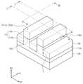
도 1, 도 3, 도 5, 도 12, 도 14 및 도 16은 본 발명의 일 실시예에 따른 반도체 소자의 제조방법을 설명하기 위한 사시도들이다. 도 2, 도 4, 도 6, 도 13, 도 15, 및 도 17은 각각 도 1, 도 3, 도 5, 도 12, 도 14 및 도 16의 Ⅰ-Ⅰ', Ⅱ-Ⅱ', 및 Ⅲ-Ⅲ' 에 따른 단면도들이다.FIGS. 1, 3, 5, 12, 14, and 16 are perspective views illustrating a method of manufacturing a semiconductor device according to an embodiment of the present invention. 2, 4, 6, 13, 15, and 17 are sectional views taken along lines I-I ', II-II', and III in FIGS. 1, 3, 5, 12, Sectional views taken along line III-III '.
도 1 및 도 2를 참조하면, 기판(100) 상에 버퍼층(110a)이 형성될 수 있고, 버퍼층(110a) 상에 핀 구조체들(FS)이 형성될 수 있다. 핀 구조체들(FS)은 제1 방향(D1)으로 연장되고, 제1 방향(D1)과 교차하는 제2 방향(D2)을 따라 배열될 수 있다. 핀 구조체들(FS) 각각은 버퍼층(110a)으로부터 위로 돌출되고 제1 방향(D1)으로 연장되는 버퍼 패턴(110b), 및 버퍼 패턴(110b)의 상면 상에 제공되어 제1 방향(D1)으로 연장되는 활성패턴(120)을 포함할 수 있다. 즉, 핀 구조체들(FS)은 제1 방향(D1) 및 제2 방향(D2) 모두에 수직한 제3 방향(D3)을 따라 버퍼층(110a)으로부터 돌출될 수 있다. 제1 방향(D1) 및 제2 방향(D2)은 기판(100)의 상면에 평행한 방향들일 수 있다.Referring to FIGS. 1 and 2, a
핀 구조체들(FS)을 형성하는 것은, 기판(100) 상에 예비 버퍼층(미도시) 및 활성층(미도시)을 차례로 형성하는 것, 및 활성층 및 예비 버퍼층을 패터닝하여 핀 구조체들(FS)을 정의하는 트렌치들(T)을 형성하는 것을 포함할 수 있다. 예비 버퍼층은 기판(100)과 다른 격자 상수를 갖는 물질을 포함할 수 있다. 예비 버퍼층의 격자 상수는 기판(100)의 격자 상수보다 클 수 있다. 일 예로, 기판(100)이 실리콘 기판인 경우, 예비 버퍼층은 실리콘-게르마늄을 포함할 수 있다. 예비 버퍼층은, 일 예로, 기판(100)을 시드로 이용하는 선택적 에피택시얼 성장(Selective Epitaxial Growth; SEG) 공정을 이용하여 형성될 수 있다. 다른 예로, 예비 버퍼층은 화학기상증착법(Chemical Vapor Deposition; CVD) 또는 분자 빔 에피택시(Molecular Beam Epitaxy: MBE) 방법을 이용하여 형성될 수 있다.The formation of the pin structures FS is accomplished by sequentially forming a buffer layer (not shown) and an active layer (not shown) on the
활성층은 예비 버퍼층과 다른 격자 상수를 갖는 물질을 포함할 수 있다. 일 실시예에 따르면, 활성층은 예비 버퍼층보다 작은 격자 상수를 갖는 물질을 포함할 수 있다. 일 예로, 예비 버퍼층은 Si1-xGex으로 형성되고, 활성층은 Si으로 형성될 수 있다. 다른 예로, 예비 버퍼층은 Si1-xGex을 포함하고, 활성층은 Si1-yGe (여기서, x>y)을 포함할 수 있다. 이에 따라, 예비 버퍼층은 활성층에 인장성 스트레인(tensile strain)을 제공할 수 있다. 이 경우, 본 발명의 반도체 소자는 NMOSFET 일 수 있다. 다른 실시예에 따르면, 활성층은 예비 버퍼층보다 큰 격자 상수를 갖는 물질을 포함할 수 있다. 일 예로, 예비 버퍼층은 Si1-xGex을 포함하고, 활성층은 Ge을 포함할 수 있다. 다른 예로, 예비 버퍼층은 Si1-zGez을 포함하고, 활성층은 Si1-wGew(여기서, z<w)을 포함할 수 있다. 이에 따라, 예비 버퍼층은 활성층에 압축성 스트레인(compressive strain )을 제공할 수 있다. 이 경우, 본 발명의 반도체 소자는 PMOSFET 일 수 있다. 예비 버퍼층과 활성층이 서로 다른 격자 상수를 가짐에 따라, 예비 버퍼층은 스트레인이 완화된 상태일 수 있는 반면, 활성층은 스트레인이 가해진 상태일 수 있다. 활성층은, 일 예로, 예비 버퍼층을 시드로 이용하는 선택적 에피택시얼 성장(Selective Epitaxial Growth; SEG) 공정을 이용하여 형성될 수 있다. 다른 예로, 활성층은 화학기상증착법(Chemical Vapor Deposition; CVD) 또는 분자 빔 에피택시(Molecular Beam Epitaxy: MBE) 방법을 이용하여 형성될 수 있다.The active layer may include a material having a different lattice constant from the spare buffer layer. According to one embodiment, the active layer may comprise a material having a smaller lattice constant than the spare buffer layer. For example, the spare buffer layer may be formed of Si1-x Gex , and the active layer may be formed of Si. As another example, the spare buffer layer may include Si1-x Gex , and the active layer may include Si1-y Ge (where x> y). Accordingly, the spare buffer layer can provide a tensile strain to the active layer. In this case, the semiconductor device of the present invention may be an NMOSFET. According to another embodiment, the active layer may comprise a material having a lattice constant greater than that of the spare buffer layer. As an example, the spare buffer layer may comprise Si1-x Gex and the active layer may comprise Ge. In another example, the spare buffer layer comprises Si1-z Gez , and the active layer may comprise Si1-w Gew (where z <w). Accordingly, the spare buffer layer can provide a compressive strain to the active layer. In this case, the semiconductor device of the present invention may be a PMOSFET. As the spare buffer layer and the active layer have different lattice constants, the spare buffer layer may be in a relaxed state while the active layer may be in a strained state. The active layer can be formed, for example, using a selective epitaxial growth (SEG) process using a spare buffer layer as a seed. In another example, the active layer may be formed using Chemical Vapor Deposition (CVD) or Molecular Beam Epitaxy (MBE).
트렌치들(T)을 형성하는 것은, 활성층 상에 핀 구조체들(FS)이 형성될 영역을 정의하는 마스크 패턴(미도시)을 형성하는 것, 및 마스크 패턴을 식각 마스크로 활성층 및 예비 버퍼층을 이방성 식각하는 것을 포함할 수 있다. 식각 공정 동안, 활성층이 식각되어 활성 패턴들(120)이 형성될 수 있고, 예비 버퍼층의 상부가 식각되어 버퍼 패턴들(110b)이 형성될 수 있다. 식각 공정 동안 식각되지 않은 예비 버퍼층의 하부는 버퍼층(110a)으로 정의될 수 있다.The formation of the trenches T includes forming a mask pattern (not shown) defining an area where pin structures FS are to be formed on the active layer, and forming the active layer and the spare buffer layer with anisotropy Etch. ≪ / RTI > During the etching process, the active layer may be etched to form the
핀 구조체들(FS)의 양 측에 소자분리막들(130)이 형성될 수 있다. 소자분리막들(130)은 트렌치들(T)을 채우도록 형성될 수 있다. 소자분리막들(130)을 형성하는 것은, 기판(100) 상에 트렌치들(T)을 채우는 절연막을 형성하는 것, 및 마스크 패턴이 노출될 때까지 절연막을 평탄화하는 것을 포함할 수 있다. 소자분리막들(130)의 상부가 리세스되어 핀 구조체들(FS)의 상부가 노출될 수 있다. 즉, 활성 패턴들(120)의 적어도 일부가 소자분리막들(130)에 의해 노출될 수 있다. 이에 따라, 소자분리막들(130)의 상면(130U)은 핀 구조체들(FS)의 상면(FS_U)(즉, 활성 패턴들(120)의 상면(120U))보다 낮을 수 있다. 소자분리막들(130)은 일 예로, 실리콘 산화물, 실리콘 질화물 또는 실리콘 산질화물을 포함할 수 있다.The
일 실시예에 따르면, 도 2에 도시된 바와 같이, 소자분리막들(130)의 상면(130U)은 활성 패턴들(120)의 하면(120L)보다 낮을 수 있다. 이 경우, 버퍼 패턴들(110b)의 상부가 소자분리막들(130)에 의해 노출될 수 있다. 다른 실시예에 따르면, 도시된 바와 달리, 소자분리막들(130)의 상면(130U)은 활성 패턴들(120)의 하면(120L)보다 높을 수 있다. 이 경우, 버퍼 패턴들(111b)은 소자분리막들(130)에 의해 노출되지 않을 수 있다. 소자분리막들(130)의 상부를 리세스하는 것은, 일 예로, 습식 식각 공정을 이용하여 수행될 수 있고, 핀 구조체들(FS)에 대하여 식각 선택성을 갖는 식각 조건을 이용하여 수행될 수 있다. 소자분리막들(130)의 상부를 리세스하는 동안, 마스크 패턴들이 제거될 수 있다.2, the
도 3 및 도 4를 참조하면, 기판(100) 상에 핀 구조체들(FS) 및 소자분리막들(130)을 덮는 식각 정지막 및 희생 게이트막이 차례로 형성될 수 있다. 식각 정지막은 일 예로, 실리콘 산화막을 포함할 수 있다. 희생 게이트막은 식각 정지막에 대하여 식각 선택성을 갖는 물질을 포함할 수 있다. 희생 게이트막은 일 예로, 폴리 실리콘을 포함할 수 있다.Referring to FIGS. 3 and 4, an etch stop layer and a sacrificial gate layer may be sequentially formed on the
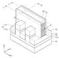
희생 게이트막을 패터닝하여, 희생 게이트 패턴(134)이 형성될 수 있다. 희생 게이트 패턴(134)은 제2 방향(D2)로 연장되어 핀 구조체들(FS)을 가로지를 수 있다. 희생 게이트 패턴(134)을 형성하는 것은, 희생 게이트막 상에 게이트 마스크 패턴(136)을 형성하는 것, 및 게이트 마스크 패턴(136)을 식각 마스크로 하여 희생 게이트막을 식각하는 것을 포함할 수 있다. 게이트 마스크 패턴(136)은 일 예로, 실리콘 질화물을 포함할 수 있다. 희생 게이트막을 식각하는 것은, 식각 정지막에 대하여 식각 선택성을 갖는 식각 공정을 수행하는 것을 포함할 수 있다.By patterning the sacrificial gate film, a
희생 게이트 패턴(134)이 형성된 후, 희생 게이트 패턴(134) 양 측의 식각 정지막을 제거하여 희생 게이트 패턴(134) 아래에 식각 정지 패턴(132)이 형성될 수 있다. 식각 정지 패턴(132)은 희생 게이트 패턴(134)의 바닥면을 따라 연장되어, 핀 구조체들(FS)의 상면 및 측벽들, 및 소자분리막들(130)의 상면들을 덮을 수 있다. 식각 정지 패턴(132), 희생 게이트 패턴(134), 및 게이트 마스크 패턴(136)은 희생 게이트 구조체로 정의될 수 있다.After the
희생 게이트 패턴(134)이 핀 구조체들(FS)을 가로지르도록 형성됨에 따라, 핀 구조체들(FS) 내에 제1 부분(P1) 및 제2 부분들(P2)이 정의될 수 있다. 제1 부분(P1)은 희생 게이트 패턴(134) 아래에 위치하고 희생 게이트 패턴(134)과 수직적으로 중첩하는 핀 구조체들(FS)의 일 부분이고, 제2 부분들(P2)은 희생 게이트 패턴(134) 양 측에 위치하고 제1 부분(P1)에 의해 수평적으로 분리된 핀 구조체들(FS)의 다른 부분들이다. 제1 부분(P1)의 상면은 제2 부분들(P2)의 각각의 상면과 실질적으로 동일 평면 상에 위치할 수 있다.As the
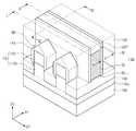
이어서, 기판(100) 상에 게이트 스페이서막(140)이 콘포말하게 형성될 수 있다. 게이트 스페이서막(140)은, 희생 게이트 패턴(134)의 양 측의 소자분리막들(130)의 상면, 핀 구조체들(FS)의 제2 부분(P2)의 상면 및 측벽들과, 희생 게이트 구조체의 상면 및 측벽들을 덮을 수 있다. 게이트 스페이서막(140)은 일 예로, 실리콘 질화물, 실리콘 탄화질화물, 또는 실리콘 산화탄화질화물을 포함할 수 있다. 게이트 스페이서막(140)은 CVD 또는 ALD와 같은 증착 공정에 의해 형성될 수 있다.Then, a
도 5 및 도 6을 참조하면, 게이트 스페이서막(140)이 패터닝되어, 희생 게이트 패턴(134)의 측벽들 상에 게이트 스페이서들(GSP)이 형성될 수 있다. 게이트 스페이서막(140)의 패터닝은 이온 빔 식각 공정을 이용하여 수행될 수 있다. 이온 빔 식각 공정의 수행 동안, 기판(100) 상으로 조사되는 이온 빔은 일정한 방향성을 가질 수 있다. 구체적으로, 이온 빔은, 평면적 관점에서, 일 방향(예를 들면, 희생 게이트 패턴(134)이 연장되는 방향)을 따라 조사될 수 있다. 이에 더하여, 이온 빔은, 일 단면의 관점에서, 기판(100)의 상면에 수직인 방향에 대해 일정 각도 범위로 기울어져 조사될 수 있다.Referring to FIGS. 5 and 6, the
이온 빔 식각 공정에 의해, 핀 구조체들(FS)의 제2 부분들(P2)의 상면, 및 희생 게이트 패턴(134)의 양 측의 소자분리막들(130)의 상면이 노출될 수 있다. 또한, 식각 공정 동안, 핀 구조체들(FS)의 제2 부분들(P2)의 측벽들이 노출될 수 있다. 식각 공정 동안 게이트 마스크 패턴(136)의 일부가 식각될 수 있고, 식각 공정 후 게이트 마스크 패턴(136)의 잔부가 희생 게이트 패턴(134) 상에 남을 수 있다. 결과적으로, 게이트 스페이서막(140)이 희생 게이트 패턴(134)의 측벽들 상에 잔존하여, 게이트 스페이서들(GSP)이 형성될 수 있다. 이하, 도 7 내지 도 11을 참조하여, 본 발명의 개념에 따른 이온 빔 식각 공정에 대해 상세히 설명한다.The upper surface of the second portions P2 of the fin structures FS and the upper surface of the
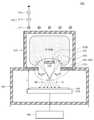
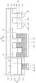
도 7은 본 발명의 개념에 따른 이온 빔 식각 공정을 수행하는 이온 빔 식각 장비의 일 예를 나타내는 개략도이다. 도 8은 도 7의 이온 빔 제어부를 설명하기 위한 평면도이고, 도 9는 도 7의 이온 빔 제어부를 통과하여 기판으로 조사되는 이온 빔을 설명하기 위한 개념도이다. 도 10 및 도 11은 본 발명의 이온 빔 식각 공정이 수행되는 상태를 설명하기 위한 도면들로, 각각 도 3의 Ⅰ-Ⅰ' 및 Ⅲ-Ⅲ' 에 따른 단면도들이다.7 is a schematic view showing an example of an ion beam etching apparatus for performing an ion beam etching process according to the concept of the present invention. FIG. 8 is a plan view for explaining the ion beam control unit of FIG. 7, and FIG. 9 is a conceptual view for explaining an ion beam irradiated to the substrate through the ion beam control unit of FIG. FIGS. 10 and 11 are views for explaining a state in which the ion beam etching process of the present invention is performed, and are cross-sectional views according to I-I 'and III-III' of FIG. 3, respectively.
도 7 내지 도 9를 참조하면, 이온 빔 식각 장비(500)는 이온 빔(IB1, IB2)을 발생시키는 소스 챔버(502), 이온 빔(IB1, IB2)을 이용한 이온 빔 식각 공정을 수행하는 공정 챔버(514), 플라즈마 생성 유닛(540) 및 바이어스 소스(550)를 포함할 수 있다. 소스 챔버(502) 및 공정 챔버(514)는 서로 연결되어 통할 수 있다. `7 to 9, the ion
소스 챔버(502) 내로 소스 가스가 공급될 수 있다. 소스 가스는 반응성 가스를 포함할 수 있다. 예를 들어, 게이트 스페이서막(140)이 질화물 계열(즉, 실리콘 질화물, 실리콘 탄화질화물, 또는 실리콘 산화탄화질화물)의 물질로 형성된 경우, 소스 가스는 플로린 계열의 식각 가스와 산소(O2) 가스의 혼합 가스를 포함할 수 있다. 플로린 계열의 식각 가스는 일 예로, CH3F, CF4, C2F6, SiF4 또는 NF3를 포함할 수 있으나, 본 발명의 실시예들이 이에 한정되는 것은 아니다. 본 발명의 개념에 따르면, 소스 가스의 산소 분율(즉, 소스 가스 내의 산소 가스의 분압 비율)은 50% 이상일 수 있다. 바람직하게, 산소 가스의 분압 비율은 50 내지 80% 일 수 있다. 산소 가스의 분압 비율이 50% 이하인 경우, 이온 빔 식각 공정의 식각 선택성이 떨어질 수 있다(즉, 게이트 스페이서막(140)과 활성 패턴들(120)의 식각 선택비가 낮아질 수 있다). 산소 가스의 분압 비율이 80% 이상인 경우, 게이트 스페이서막(140)의 식각률이 감소될 수 있다.Source gas may be supplied into the
플라즈마 생성 유닛(540)은 소스 챔버(502) 내로 공급된 소스 가스를 플라즈마(PLASMA)로 변환시킬 수 있다. 소스 챔버(502) 내부의 플라즈마(PLASMA)는 이온 빔(IB1, IB2)의 소스가 될 수 있다. 일 실시예에 있어서, 플라즈마 생성 유닛(540)은 플라즈마 파워 생성기(546) 및 플라즈마 파워 생성기(546)에 연결된 전극(542)을 포함할 수 있다. 플라즈마 파워 생성기(546)는 플라즈마 파워를 생성하여 전극(542)에 인가할 수 있다. 예컨대, 플라즈마 파워는 라디오 주파수 파워(radio frequency (RF) power)일 수 있다. 전극(542)은 폐루프 형태 또는 코일형태일 수 있다. 플라즈마(PLASMA)는 전극(542)에 인가된 플라즈마 파워에 의해 유도될 수 있다. 플라즈마 파워(즉, RF 파워)는 요구되는 플라즈마(PLASMA)의 밀도에 따라 다양하게 조절될 수 있다. 본 발명의 개념에 따른 이온 빔 식각 공정은 일 예로, 0.5 내지 10kW의 플라즈마 파워를 이용하여 수행될 수 있으나, 본 발명의 실시예들이 이에 한정되는 것은 아니다.The
이에 더하여, 플라즈마 생성 유닛(540)은 플라즈마 파워 생성기(546) 및 전극(542) 사이에 연결된 매칭 유닛(544, matching unit)을 더 포함할 수 있다. 플라즈마 파워는 플라즈마 파워 생성기(546)로부터 매칭 유닛(544)을 통하여 전극(542)에 전달될 수 있다. 매칭 유닛(544)은 플라즈마 파워의 전달 효율을 증가시킬 수 있다. 하지만, 본 발명은 상술된 플라즈마 생성 유닛(540)에 한정되지 않는다. 즉, 플라즈마 생성 유닛(540)는 플라즈마를 생성시키는 다른 형태로 구현될 수도 있다.In addition, the
공정 챔버(514)는 식각 대상이 되는 기판(100)을 로드하기 위한 스테이지(510)를 포함할 수 있다. 스테이지(510)는 스테이지(510)의 상면에 수직한 회전축을 따라 회전 가능하도록 구성되고, 스테이지(510)의 상면에 평행한 직교 좌표축을 따라 직선 이동 가능하도록 구성될 수 있다. 또한, 스테이지(510)는 그의 상면에 수직한 방향으로 직선 이동 가능하도록 구성될 수 있다. 스테이지(510)의 회전 및 직선 이동에 의해, 스테이지(510) 상의 기판(100) 또한 회전 및 직선 이동될 수 있다. 이온 빔 식각 공정이 수행되는 동안, 스테이지(510)는 x 방향(도 8 참조) 또는 x 방향의 반대 방향으로 직선 이동될 수 있다.The process chamber 514 may include a
바이어스 소스(550)는 기판(100)에 이온 추출 전압(ion extraction voltage)을 인가할 수 있다. 본 발명의 실시예들에 따른 이온 빔 식각 공정은 일 예로, 200 내지 1000 V의 이온 추출 전압을 이용하여 수행될 수 있다. 기판(100)에 이온 추출 전압이 인가됨에 따라, 플라즈마(PLASMA)로부터 제공되는 이온들이 플라즈마 쉬스(plasma sheath, 520)를 가로질러 기판(100)으로 조사될 수 있다. 기판(100)으로 조사되는 이온들은 이온 빔(IB1, IB2)을 구성할 수 있다. 여기서, 플라즈마 쉬스(520)는 플라즈마(PLASMA)와 기판(100) 사이에 플라즈마(PLASMA)보다 적은 수의 전자들을 갖는 일 영역으로 정의될 수 있다. 본 발명이 개념에 따르면, 바이어스 소스(550)는 펄스 방식으로 구동될 수 있다. 일 예로, 바이어스 소스(550)는 펄스 DC 파워 서플라이(Pulsed DC Power Supply)일 수 있다. 그러나, 본 발명의 실시예들이 이에 한정되는 것은 아니다. 기판(100)에 인가되는 이온 추출 전압은 일정한 주기로 온(on)/오프(off)될 수 있다. 본 발명의 실시예들에 따른 이온 빔 식각 공정에서, 이온 추출 전압의 듀티 사이클(duty cycle)은 50 내지 75% 일 수 있다. 여기서, 듀티 사이클(duty cycle)은 이온 추출 전압이 온(on)/오프(off) 되는 주기에서 이온 추출 전압이 온(on) 상태인 시간의 비율로 정의될 수 있다.The
상술한 산소 가스의 분압 비율과 함께, 이온 추출 전압의 듀티 사이클을 제어하여, 게이트 스페이서막(140)과 활성 패턴들(120)의 식각 선택비를 조절할 수 있다. 본 실시예에서, 활성 패턴들(120)에 대한 게이트 스페이서막(140)의 식각 선택비는 20:1 내지 50:1 일 수 있다.The etch selectivity of the
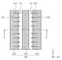
소스 챔버(502) 내부에 이온 빔 제어부(530)가 제공될 수 있다. 이온 빔 제어부(530)는, 수평적으로 서로 이격되어 제공되고, 기판(100)으로부터 동일한 레벨에 위치하는 제1 절연체(532) 및 제2 절연체(534)를 포함할 수 있다. 일 예로, 제1 및 제2 절연체들(532, 534)은 스테이지(510)로부터 일 거리(d)만큼 이격될 수 있다. 스테이지(510)와 제1 및 제2 절연체들(532, 534) 사이의 간격(d)은 스테이지(510)의 수직 이동에 의해 조절될 수 있다. 일 실시예에 따르면, 스테이지(510)와 제1 및 제2 절연체들(532, 534) 사이의 간격(d)은 0(zero) 보다 크되, 100mm 이하 일 수 있다. 이하, 스테이지(510)와 제1 및 제2 절연체들(532, 534) 사이의 간격(d)은 Z-갭(d)으로 지칭될 수 있다.An
이온 빔 제어부(530)는 제1 절연체(532) 및 제2 절연체(534) 사이에 제공되고, 제1 절연체(532) 및 제2 절연체(534)보다 기판(100)으로부터 높은 레벨에 위치하는 제3 절연체(536)를 더 포함할 수 있다. 절연체들(532, 534, 536)은 일 예로, 석영(quartz), 유리, 실리콘 질화물 등으로 형성될 수 있다. 도 8에 도시된 바와 같이, 평면적 관점에서, 제1 내지 제3 절연체들(532, 534, 536)각각은 일 방향(즉, y 방향)으로 연장되는 바 형태를 가질 수 있다. 그러나, 본 발명의 개념은 이에 한정되지 않고, 제1 내지 제3 절연체들(532, 534, 536)은 다양한 형태를 가질 수 있다. 이온 빔 제어부(530)는 플라즈마 시스(520) 내의 전기장(520E)의 형태를 변경시켜, 플라즈마(PLASMA)와 플라즈마 시스(520) 사이의 경계선(524)의 형태를 제어할 수 있다. 일 실시예에 따르면, 플라즈마(PLASMA)는 기판(100) 상에 제공될 수 있고, 이온 빔 제어부(530)는 플라즈마(PLASMA)와 기판(100) 사이에 제공될 수 있다. 이온 빔 제어부(530)는 플라즈마(PLASMA)와 플라즈마 시스(520) 사이의 경계선(524)의 형태를 제어함으로써, 스테이지(510) 상에 로드된 기판(100)의 표면 상으로 조사되는 이온 빔(IB1, IB2)의 형태 및 그의 입사각을 제어할 수 있다.The
상세하게, 플라즈마(PLASMA)로부터 제공되는 이온들은 제1 절연체(532)와 제3 절연체(536) 사이의 경계선(524)을 가로질러 제1 절연체(532)와 제3 절연체(536) 사이의 제1 갭 영역(G1)을 통해 기판(100) 상으로 조사될 수 있다. 더하여, 플라즈마(PLASMA)로부터 제공되는 이온들은 제2 절연체(534)와 제3 절연체(536) 사이의 경계선(524)을 가로질러 제2 절연체(534)와 제3 절연체(536) 사이의 제2 갭 영역(G2)을 통해 기판(100) 상으로 조사될 수 있다. 제1 갭 영역(G1)을 통해 기판(100) 상으로 조사되는 이온들은 제1 이온 빔(IB1)을 구성할 수 있고, 제2 갭 영역(G2)을 통해 기판(100) 상으로 조사되는 이온들은 제2 이온 빔(IB2)을 구성할 수 있다. 제1 및 제2 이온 빔들(IB1, IB2)은 기판(100) 상으로 동시에 조사될 수 있다.The ions provided from the plasma PLASMA are applied to the
한편, 도 8에 도시된 바와 같이, 갭 영역들(G1, G2)은 절연체들(532, 534, 536)의 연장 방향(예를 들어, y 방향)으로 장축을 갖는 장방형 형상을 가질 수 있다. 즉, 평면적 관점에서, 갭 영역들(G1, G2)은, 단축 방향(예를 들어, x 방향)에 따른 폭 및 장축 방향(예를 들어, y 방향)에 따른 길이를 가질 수 있다. 갭 영역들(G1, G2)의 길이는 일 예로, 기판(100)의 직경과 같거나 클 수 있다. 갭 영역들(G1, G2)을 통과하는 이온 빔(IB1, IB2)은 상술한 갭 영역들(G1, G2)의 폭 및 길이에 대응하는 범위로 기판(100) 상의 일 영역에 조사될 수 있다. 즉, 이온 빔(IB1, IB2) 은 리본 빔 형태로 구현될 수 있다. 리본 빔 형태로 구현되는 이온 빔(IB1, IB2)은 복수의 빔렛들(BL1, BL2)을 포함할 수 있다.8, the gap regions G1 and G2 may have a rectangular shape having a long axis in the extending direction (for example, the y direction) of the
평면적 관점에서, 제1 이온 빔(IB1)의 빔렛들(BL1)은 x 방향으로 조사될 수 있고, 제2 이온 빔(IB2)의 빔렛들(BL2)은 x 방향의 반대 방향(즉, -x 방향)으로 조사될 수 있다.From a plan viewpoint, the beamlets BL1 of the first ion beam IB1 may be irradiated in the x direction and the beamlets BL2 of the second ion beam IB2 may be irradiated in the direction opposite to the x direction (i.e., -x Direction).
이에 더하여, 이온 빔(IB1, IB2)의 빔렛들(BL1, BL2)은, 일정 각도 범위 내에서, 기판(100)의 상면에 수직한 법선(100S)에 대해 기울어져 조사될 수 있다. 즉, 이온 빔(IB1, IB2)은 입사각 범위(range of incident angle)를 가질 수 있다. 예를 들어, 도 9에 도시된 바와 같이, 제1 이온 빔(IB1)은 서로 다른 제1 내지 제3 입사각들(a1, a2, a3)을 갖는 빔렛들(BL1)을 포함할 수 있다. 이 때, 제1 입사각(a1)이 제1 이온 빔(IB1)의 최소 입사각에 해당하고, 제3 입사각(a3)이 제1 이온 빔(IB1)의 최대 입사각에 해당하는 경우, 제1 이온 빔(IB1)은 제1 입사각(a1)과 제3 입사각(a3) 사이의 제1 입사각 범위를 가질 수 있다. 마찬가지로, 제2 이온 빔(IB2)은 서로 다른 제4 내지 제6 입사각들(b1, b2, b3)을 갖는 빔렛들(BL2)을 포함할 수 있다. 이 때, 제4 입사각(b1)이 제2 이온 빔(IB2)의 최소 입사각에 해당하고, 제6 입사각(b3)이 제2 이온 빔(IB2)의 최대 입사각에 해당하는 경우, 제2 이온 빔(IB2)은 제4 입사각(b1)과 제6 입사각(b3) 사이의 제2 입사각 범위를 가질 수 있다. 일 실시예에 따르면, 제1 이온 빔(IB1)의 제1 입사각의 범위는 제2 이온 빔(IB2)의 제2 입사각의 범위와 실질적으로 동일할 수 있다. 이 경우, 제1 이온 빔(IB1)과 제2 이온 빔(IB2)는 법선(100S)을 기준으로 서로 대칭될 수 있다. 일 예로, 제1 이온 빔(IB1)의 제1 입사각의 범위 및 제2 이온 빔(IB2)의 제2 입사각의 범위의 각각은 0도 보다 크고 60도 작을 수 있다. 바람직하게, 제1 입사각의 범위 및 제2 입사각의 범위의 각각은 10 내지 50도 일 수 있다.In addition, the beamlets BL1 and BL2 of the ion beams IB1 and IB2 can be irradiated with inclination with respect to the
이와 같은 제1 입사각의 범위 및 제2 입사각의 범위는 핀 구조체들(FS) 사이의 간격, 게이트 스페이서막(149)의 두께, 및 핀 구조체들(FS)와 소자분리막들(130)의 단차 등을 고려하여 설계될 수 있다. 더하여, 빔렛들(BL1, BL2) 각각의 입사각은 혹은 이온 빔(IB1, IB2)의 입사각의 범위는, 플라즈마 파워, 이온 빔 추출 전압 또는 Z-갭(d) 등과 같은 다양한 공정 파라미터들에 의해 조절될 수 있다.The range of the first angle of incidence and the range of the second angle of incidence are set such that the distance between the fin structures FS, the thickness of the gate spacer film 149, and the step height of the pin structures FS and the
본 발명의 개념에 따른 이온 빔 식각은 상술한 이온 빔 식각 장비(500)에서 수행될 수 있다. 상세하게, 게이트 스페이서막(140)이 형성된 기판(100)이 이온 빔 식각 장비(500)의 스테이지(510)에 로딩될 수 있다. 이 때, 스테이지(510) 상의 기판(100)은, 희생 게이트 패턴(134)의 연장 방향이 갭 영역들(G1, G2)의 단축 방향(즉, x 또는 -x 방향)과 평행하도록 정렬될 수 있다. 기판(100)의 정렬은 일 예로, 스테이지(510)이 회전에 의해 수행될 수 있다. 이 후, 정렬된 기판(100) 상으로 이온 빔(IB1, IB2)이 조사될 수 있다. 희생 게이트 패턴(134)의 연장 방향이 갭 영역들(G1, G2)의 단축 방향과 평행하도록 정렬됨에 따라, 이온 빔(IB1, IB2)은, 평면적 관점에서, 희생 게이트 패턴(134)의 연장 방향을 따라 기판(100) 상에 조사될 수 있다. 즉, 도 10 및 도 11에 도시된 바와 같이, 이온 빔(IB1, IB2)은, 핀 구조체들(FS)의 제2 방향(D2)으로 마주하는 측벽들 상으로 기울어져 조사될 수 있고, 희생 게이트 패턴(134)의 제1 방향(D1)으로 마주하는 측벽들 상으로는 조사되지 않을 수 있다. 더하여, 이온 빔(IB1, IB2)은 핀 구조체들(FS)의 상면, 희생 게이트 패턴(134)의 상면, 및 희생 게이트 패턴(134) 양 측의 소자분리막들의 상면 상으로 조사될 수 있다. 이온 빔 식각 공정이 수행되는 동안, 이온 빔(IB1, IB2)이 기판(100)의 전 영역에 골고루 조사되도록 기판(100)이 스캐닝될 수 있다. 기판(100)의 스캐닝은 스테이지(510)의 x 또는 -x 방향에 따른 직선 이동에 의해 수행될 수 있다. 기판(100)의 스캐닝은, 희생 게이트 패턴(134)의 양 측의 소자분리막들(130)의 상면, 핀 구조체들(FS)의 제2 부분들(P2)의 상면 및 측벽들과, 게이트 마스크 패턴(136)의 상면이 노출될 때까지 반복 수행될 수 있다.The ion beam etching according to the concept of the present invention can be performed in the ion
일반적으로, 기판(100)의 상면에 수직한 방향으로 식각이 진행되는 이방성 식각(예를 들어, 반응성 이온 식각) 방법을 이용하여 게이트 스페이서(GSP)를 형성하는 경우, 핀 구조체들(FS)의 상면 및 희생 게이트 패턴(134)의 상면 상의 게이트 스페이서막(140)이 전부 제거된 후에도, 핀 구조체들(FS)의 측벽들 상의 게이트 스페이서막(140)을 식각하기 위한 식각이 계속될 수 있다. 이에 따라, 먼저 노출된 핀 구조체들(FS)의 상부가 과식각될 수 있고, 희생 게이트 패턴(134)의 측벽들 상의 게이트 스페이서막(140)도 과식각될 수 있다. 핀 구조체들(FS)의 상부가 과식각되어 핀 구조체들(FS)의 높이가 낮아지면, 후술할 클래딩층들(145)의 형성 공정의 공정 마진이 감소될 수 있다. 그러나, 본 발명의 개념에 따른 이온 빔 식각 공정으로 게이트 스페이서막(140)을 제거하는 경우, 핀 구조체들(FS)의 측벽들 상의 게이트 스페이서막(140)이 효과적으로 제거되어, 핀 구조체들(FS)의 손상을 최소화하면서 게이트 스페이서들(GSP)을 형성할 수 있다. 나아가, 게이트 스페이서(GSP)의 손상도 최소화될 수 있다. 이어서, 본 발명의 일 실시예에 따른 반도체 소자의 제조 방법에 대해 계속 설명한다.In general, when a gate spacer (GSP) is formed using an anisotropic etching (for example, a reactive ion etching) method in which etching is performed in a direction perpendicular to the upper surface of the
도 12 및 도 13을 참조하면, 희생 게이트 패턴(134)의 양 측에 클래딩층들(145)이 형성될 수 있다. 클래딩층들(145)은 핀 구조체들(FS)의 제2 부분들(P2) 상에 각각 형성될 수 있다. 클래딩층들(145)의 각각은 핀 구조체들(FS)의 제2 부분들(P2)의 각각의 상면 및 측벽들을 덮을 수 있다. 즉, 클래딩층들(145)의 각각은 활성 패턴들(120)의 제2 영역들(R2)의 각각의 상면 및 측벽들을 덮을 수 있다.Referring to FIGS. 12 and 13, cladding layers 145 may be formed on both sides of the
클래딩층들(145)을 형성하는 것은, 소자분리막들(130)에 의해 노출된 핀 구조체들(FS)의 상부를 시드로 이용하여 선택적 에피택시얼 성장 공정을 수행하는 것을 포함할 수 있다. 즉, 클래딩층들(145)은 에피택시얼층일 수 있다. 클래딩층들(145)이 PMOSFET을 구성하는 경우, 클래딩층들(145)은 활성 패턴들(120)에 압축성 스트레인을 제공하는 물질로 형성될 수 있다. 일 예로, 활성 패턴들(120)이 SiGe을 포함하는 경우, 클래딩층들(145)은 활성 패턴들(120)보다 큰 격자 상수를 갖는 SiGe층(즉, 활성 패턴들(120)보다 높은 게르마늄 농도를 갖는 SiGe층)으로 형성될 수 있다. 이와 달리, 클래딩층들(145)이 NMOSFET을 구성하는 경우, 클래딩층들(145)은 활성 패턴들(120)에 인장성 스트레인을 제공하는 물질로 형성될 수 있다. 일 예로, 활성 패턴들(120)이 SiGe을 포함하는 경우, 클래딩층들(145)은 활성 패턴들(120)보다 격자 상수가 작은 Si층 또는 SiC층으로 형성되거나, 활성 패턴들(120)보다 게르마늄 농도가 낮은 SiGe층으로 형성될 수 있다. 그러나, 본 발명의 실시예들이 이에 한정되는 것은 아니다.The formation of the cladding layers 145 may include performing a selective epitaxial growth process using the top of the fin structures FS exposed by the
클래딩층들(145) 각각은 기판(100)의 상면에 대해 실질적으로 네거티브하게 경사진 제1 측벽(145S1), 기판(100)의 상면에 대해 실질적으로 포지티브하게 경사진 제3 측벽(145S3), 및 이들 사이의 제2 측벽(145S2)을 가질 수 있다. 제2 측벽(145S2)은 기판(100)의 상면에 실질적으로 수직할 수 있으나, 본 발명의 실시예들이 이에 한정되는 것은 아니다. 기판(100)에 인접한 제2 측벽(145S2)의 일단은 제1 측벽(145S1)의 일단에 연결되고, 제2 측벽(145S2)의 타단은 제3 측벽(145S3)의 일단에 연결될 수 있다. 일 단면의 관점에서, 제2 측벽(145S2)의 길이는 제1 및 제3 측벽들(145S1, 145S3) 각각의 길이보다 클 수 있다. 여기서, 일 단면에 따른 제1 내지 제3 측벽들(145S~145S3)의 길이는 제1 내지 제3 측벽들(145S~145S3)의 단면 프로파일을 따라 측정한 길이로 정의될 수 있다. 본 발명의 개념에 따르면, 게이트 스페이서들(GSP)의 형성 동안 핀 구조체들(FS)의 제2 부분들(P2)의 손실이 최소화됨에 따라, 에피택시얼 성장 공정의 수행 시, 클래딩층들(145)의 측방 성장이 억제될 수 있다. 이에 따라, 상술한 바와 같은 클래딩층들(145)의 측벽 형상이 구현될 수 있다. 한편, 서로 인접한 클래딩층들(145)이 서로 다른 타입의 MOSFET을 구성하는 경우, 이들이 서로 연결되는 것을 방지할 필요가 있다. 본 발명의 개념에 따르면, 클래딩층들(145)의 형성 시, 그의 측방 성장이 억제되므로 서로 인접한 핀 구조체들(FS) 상의 클래딩층들(145)이 서로 접하여 연결되는 것이 방지될 수 있다. 결과적으로, 클래딩층들(145) 형성을 위한 공정의 공정 마진이 증대될 수 있다.Each of the cladding layers 145 includes a first sidewall 145S1 that is substantially tilted negatively with respect to the top surface of the
클래딩층들(145)에 불순물을 도핑시켜 소스/드레인 영역들(SD)을 형성할 수 있다. 예를 들면, 클래딩층들(145)은 선택적 에피택시얼 성장 공정과 동시에 또는 선택적 에피택시얼 성장 공정 후, 인 또는 아세닉 같은 n형의 불순물, 혹은 보론과 같은 p형의 불순물로 도핑될 수 있다. 일 실시예에 따르면, 불순물 도핑 공정 중에 핀 구조체들(FS)의 제2 부분들(P2)의 일부도 불순물로 도핑될 수 있다. 그러나, 이 경우, 제2 부분들(P2)의 불순물의 도핑 농도는 충분하지 않을 수 있다. 본 발명의 개념에 따르면, 클래딩층들(145)의 형성 전에, 핀 구조체들(FS)의 제2 부분들(P2)에 n형 또는 p형의 불순물을 도핑하는 불순물 도핑 공정이 수행될 수 있다. 이에 따라, 핀 구조체들(FS)의 제2 부분들(P2)은 충분한 불순물의 도핑 농도를 가질 수 있다. 클래딩층들(145) 및 불순물이 도핑된 제2 부분들(P2)의 일부는 소스/드레인 영역들(SD)로 정의될 수 있다. 핀 구조체들(FS)의 제2 부분들(P2)이 충분한 불순물의 도핑 농도를 가짐에 따라, 소스/드레인 영역들(SD)의 전기적 특성이 향상될 수 있다. 핀 구조체들(FS)의 제2 부분들(P2)의 불순물 도핑은, 일 예로, ALD 도핑, 플라즈마 도핑, 이온 주입 또는 MLD(monolayer doing) 방식에 의해 수행될 수 있다. 결과적으로, 소스/드레인 영역들(SD)은 희생 게이트 패턴(134)의 양 측에 형성될 수 있다.The cladding layers 145 may be doped with impurities to form the source / drain regions SD. For example, the cladding layers 145 may be doped with an n-type impurity such as phosphorus or arsenic, or a p-type impurity such as boron, either simultaneously with the selective epitaxial growth process or after the selective epitaxial growth process have. According to one embodiment, a portion of the second portions P2 of the pin structures FS during the impurity doping process may also be doped with impurities. However, in this case, the doping concentration of the impurities of the second portions P2 may not be sufficient. According to the concept of the present invention, before the formation of the cladding layers 145, an impurity doping process may be performed in which the second portions P2 of the fin structures FS are doped with n-type or p-type impurities . Accordingly, the second portions P2 of the pin structures FS can have a doping concentration of sufficient impurities. Cladding layers 145 and portions of the second portions P2 doped with impurities may be defined as source / drain regions SD. The electrical characteristics of the source / drain regions SD can be improved as the second portions P2 of the pin structures FS have sufficient doping concentration of impurities. Impurity doping of the second portions P2 of the pin structures FS can be performed by, for example, ALD doping, plasma doping, ion implantation, or MLD (monolayer doing) method. As a result, the source / drain regions SD may be formed on both sides of the
도 14 및 도 15를 참조하면, 소스/드레인 영역들(SD)이 형성된 기판(100) 상에 하부 층간 절연막(150)이 형성될 수 있다. 하부 층간 절연막(150)은 소스/드레인 영역들(SD) 및 희생 게이트 패턴(134)을 덮도록 형성될 수 있다. 하부 층간 절연막(150)은 클래딩층들(145)도 덮을 수 있다, 하부 층간 절연막(150)은 실리콘 산화막, 실리콘 질화막, 실리콘 산질화막, 또는 저유전막들 중 적어도 하나를 포함할 수 있다.Referring to FIGS. 14 and 15, a lower
이어서, 게이트 마스크 패턴(136), 희생 게이트 패턴(134), 및 식각 정지 패턴(132)이 제거되어, 게이트 스페이서들(GSP) 사이에 게이트 영역(160)이 형성될 수 있다. 게이트 영역(160)은 핀 구조체들(FS)의 제1 부분(P1)을 노출할 수 있다. 게이트 마스크 패턴(136)을 제거하는 식각 공정 동안, 하부 층간 절연막(150)의 일부가 식각될 수 있다. 게이트 영역(160)을 형성하는 것은, 게이트 스페이서들(GSP), 하부 층간절연막(150), 및 식각 정지 패턴(132)에 대하여 식각 선택성을 갖는 식각 공정을 수행하여 희생 게이트 패턴(134)을 식각하는 것을 포함할 수 있다. 더하여, 게이트 영역(160)을 형성하는 것은, 식각 정지 패턴(132)을 제거하여 핀 구조체들(FS)의 제1 부분(P1)을 노출하는 것을 포함할 수 있다.The
도 16 및 도 17을 참조하면, 게이트 영역(160)을 채우는 게이트 절연 패턴(GD) 및 게이트 전극(GE)이 형성될 수 있다. 구체적으로, 게이트 영역(160)을 포함하는 기판(100) 상에 게이트 절연막(미도시)이 형성되어, 게이트 영역(160)의 일부를 채울 수 있다. 게이트 절연막은 핀 구조체들(FS)의 제1 부분(P1)을 덮도록 형성될 수 있다. 게이트 절연막은 고유전막들 중 적어도 하나를 포함할 수 있다. 일 예로, 게이트 절연막은 하프늄 산화물, 하프늄 실리케이트, 지르코늄 산화물, 또는 지르코늄 실리케이트 중 적어도 하나를 포함할 수 있으나, 이러한 물질들에 한정되는 것은 아니다. 게이트 절연막은 일 예로, 원자층 증착 공정 또는 회학 기상 증착 공정을 수행하여 형성될 수 있다. 게이트 절연막 상에 게이트 막(미도시)이 형성되어, 게이트 영역(160)의 잔부를 채울 수 있다. 게이트 막은 도전성 금속 질화물(일 예로, 티타늄 질화물, 탄탈륨 질화물, 또는 텅스텐 질화물) 및 금속(일 예로, 알루미늄, 또는 텅스텐) 중 적어도 하나를 포함할 수 있다. 차례로 적층된 게이트 절연막 및 게이트 막을 평탄화하여 게이트 절연 패턴(GD) 및 게이트 전극(GE)이 형성될 수 있다. 평탄화 공정에 의해 하부 층간절연막(150) 및 게이트 스페이서들(GSP)의 상면들이 노출될 수 있다. 게이트 절연 패턴(GD)은 게이트 전극(GE)의 바닥면을 따라 연장될 수 있고, 게이트 전극(GE)의 양 측벽들 상으로 연장되어 게이트 전극(GE)과 게이트 스페이서들(GSP) 사이에 개재될 수 있다.16 and 17, a gate insulating pattern GD and a gate electrode GE filling the
게이트 전극(GE)의 상부가 리세스될 수 있다. 리세스 공정 동안, 게이트 절연 패턴(GD)의 상부도 제거될 수 있고, 이에 따라, 게이트 영역(160) 내에 리세스 영역이 정의될 수 있다. 리세스 영역 내에 게이트 캐핑 패턴(GP)이 형성될 수 있다. 게이트 캐핑 패턴(GP)을 형성하는 것은, 하부 층간 절연막(150) 상에 리세스 영역을 채우는 캐핑막을 형성하는 것, 및 하부 층간 절연막(150)이 노출될 때까지 캐핑막을 평탄화하는 것을 포함할 수 있다. 게이트 캐핑 패턴(GP)은 일 예로, 실리콘 질화물을 포함할 수 있다.The upper portion of the gate electrode GE can be recessed. During the recess process, the upper portion of the gate insulation pattern GD can also be removed, so that a recess region can be defined in the
게이트 절연 패턴(GD), 게이트 전극(GE), 게이트 캐핑 패턴(GP), 및 게이트 스페이서들(GSP)은 게이트 구조체(GS)로 정의될 수 있다. 게이트 구조체(GS)는 제2 방향(D2)으로 연장될 수 있다,The gate insulating pattern GD, the gate electrode GE, the gate capping pattern GP, and the gate spacers GSP may be defined as a gate structure GS. The gate structure GS may extend in the second direction D2,
일 실시예에 따르면, 게이트 구조체(GS)를 포함하는 기판(100) 상에 상부 층간 절연막(미도시)이 형성될 수 있다. 상부 층간 절연막은 산화물, 질화물, 및/또는 산질화물을 포함할 수 있다. 상부 층간 절연막 및 하부 층간 절연막(150)을 관통하여 소스/드레인 영역들(SD)을 노출하는 제1 콘택 홀들(미도시)이 형성될 수 있다. 제1 콘택 홀들을 형성하는 식각 공정에 의해, 소스/드레인 영역들(SD)의 상부가 부분적으로 제거될 수 있다. 상부 층간 절연막 및 하부 층간 절연막(150)을 관통하여 게이트 전극(GE)을 노출하는 제2 콘택 홀(미도시)이 형성될 수 있다. 이 후, 제1 콘택 홀들을 채우는 제1 콘택 플러그들, 및 제2 콘택 홀을 채우는 제2 콘택 플러그가 형성될 수 있다. 상부 층간 절연막 상에 제1 및 제2 콘택 플러그들에 접속하는 배선들이 형성될 수 있다. 배선들및 제1 및 제2 콘택 플러그들을 통해 소스/드레인 영역들(SD) 및 게이트 전극(GE)에 전압을 인가하도록 구성될 수 있다. 제1 및 제2 콘택 플러그들 및 배선들은 도전 물질을 포함할 수 있다.According to one embodiment, an upper interlayer insulating film (not shown) may be formed on the
본 발명의 개념에 따르면, 핀 구조체는 버퍼 패턴 및 활성 패턴을 포함할 수 있고, 활성 패턴의 격자 상수는 버퍼 패턴의 격자 상수와 다를 수 있다. 이에 따라, 버퍼 패턴은 활성 패턴에 인장성 또는 압축성 스트레스를 제공할 수 있다. 활성 패턴은 핀 구조체 상에 형성된 트랜지스터의 채널로 기능할 수 있다. 버퍼 패턴이 활성 패턴에 인장성 또는 압축성 스트레스를 제공함에 따라, 채널 특성이 개선된 반도체 소자의 제조 방법이 제공될 수 있다.According to the concept of the present invention, the pin structure may include a buffer pattern and an active pattern, and the lattice constant of the active pattern may be different from the lattice constant of the buffer pattern. Thus, the buffer pattern can provide tensile or compressive stress to the active pattern. The active pattern can function as a channel of the transistor formed on the pin structure. As the buffer pattern provides tensile or compressive stress to the active pattern, a method of manufacturing a semiconductor device with improved channel characteristics can be provided.
더하여, 일정한 방향성을 갖는 이온 빔을 이용한 식각 공정으로 희생 게이트 패턴의 측벽들 상에 게이트 스페이서를 형성함에 따라, 희생 게이트 패턴 양 측의 핀 구조체의 식각 손상이 최소화될 수 있다. 이에 따라, 희생 게이트 패턴 양 측의 핀 구조체 상에 형성되는 클래딩층이 핀 구조체로부터 균일하게 성장되어 클래딩층의 형성 공정의 공정 마진이 증대될 수 있다. 결과적으로, 전기적 특성이 향상되고, 클래딩층 형성 공정의 공정 마진이 증대된 반도체 소자의 제조 방법이 제공될 수 있다.In addition, etch damage of the fin structure on both sides of the sacrificial gate pattern can be minimized by forming gate spacers on the sidewalls of the sacrificial gate pattern by an etching process using an ion beam having a certain directionality. As a result, the cladding layer formed on the pin structure on both sides of the sacrificial gate pattern can be uniformly grown from the fin structure, and the process margin in the process of forming the cladding layer can be increased. As a result, a method of manufacturing a semiconductor device in which the electrical characteristics are improved and the process margin of the cladding layer forming process is increased can be provided.
도 18은 본 발명의 실시예들에 따른 반도체 소자를 포함하는 시모스 에스램 셀(CMOS SRAM cell)의 등가 회로도이다. 도 18을 참조하면, 시모스 에스램 셀은 한 쌍의 구동 트랜지스터들(driver transistors: TD1, TD2), 한 쌍의 전송 트랜지스터들(transfer transistors: TT1, TT2), 및 한 쌍의 부하 트랜지스터들(load transistors: TL1, TL2)을 포함할 수 있다. 구동 트랜지스터들(TD1, TD2)은 풀다운 트랜지스터(pull-down transistor)일 수 있고, 전송 트랜지스터들(TT1, TT2)은 패스 트랜지스터(paSS transistor)일 수 있고, 부하 트랜지스터들(TL1, TL2)은 풀업 트랜지스터(pull-up transistor)일 수 있다. 구동 트랜지스터들(TD1, TD2) 및 전송 트랜지스터들(TT1, TT2)은 NMOS 트랜지스터들일 수 있고, 부하 트랜지스터들(TL1, TL2)은 PMOS 트랜지스터들일 수 있다. 본 발명의 실시예들에 따른 트랜지스터들은 구동 트랜지스터들(TD1, TD2), 전송 트랜지스터들(TT1, TT2) 및 부하 트랜지스터들(TL1, TL2) 중의 하나일 수 있다.18 is an equivalent circuit diagram of a CMOS SRAM cell including a semiconductor device according to embodiments of the present invention. Referring to FIG. 18, a CMOS circuit includes a pair of driver transistors (TD1 and TD2), a pair of transfer transistors (TT1 and TT2), and a pair of load transistors transistors: TL1, TL2). The driving transistors TD1 and TD2 may be pull-down transistors, the transfer transistors TT1 and TT2 may be paSS transistors and the load transistors TL1 and TL2 may be pull- May be a pull-up transistor. The driving transistors TD1 and TD2 and the transfer transistors TT1 and TT2 may be NMOS transistors and the load transistors TL1 and TL2 may be PMOS transistors. The transistors according to embodiments of the present invention may be one of the driving transistors TD1 and TD2, the transfer transistors TT1 and TT2 and the load transistors TL1 and TL2.
제1 구동 트랜지스터(TD1)와 제1 전송 트랜지스터(TT1)는 서로 직렬로 연결될 수 있다. 제1 구동 트랜지스터(TD1)의 소스 영역은 접지선(VSS)에 전기적으로 연결되고, 제1 전송 트랜지스터(TT1)의 드레인 영역은 제1 비트 라인(BL1)에 전기적으로 연결될 수 있다. 제2 구동 트랜지스터(TD2)와 제2 전송 트랜지스터(TT2)는 직렬로 연결될 수 있다. 제2 구동 트랜지스터(TD2)의 소스 영역은 접지선(VSS)에 전기적으로 연결되고, 제2 전송 트랜지스터(TT2)의 드레인 영역은 제2 비트 라인(BL2)에 전기적으로 연결될 수 있다.The first driving transistor TD1 and the first transfer transistor TT1 may be connected in series with each other. The source region of the first driving transistor TD1 may be electrically connected to the ground line VSS and the drain region of the first transfer transistor TT1 may be electrically connected to the first bit line BL1. The second driving transistor TD2 and the second transfer transistor TT2 may be connected in series. The source region of the second driving transistor TD2 may be electrically connected to the ground line VSS and the drain region of the second transfer transistor TT2 may be electrically connected to the second bit line BL2.
제1 부하 트랜지스터(TL1)의 소스 영역 및 드레인 영역은 각각 전원선(Vcc) 및 제1 구동 트랜지스터(TD1)의 드레인 영역에 전기적으로 연결될 수 있다. 제2 부하 트랜지스터(TL2)의 소스 영역 및 드레인 영역은 전원선(Vcc) 및 제2 구동 트랜지스터(TD2)의 드레인 영역에 전기적으로 연결될 수 있다. 제1 부하 트랜지스터(TL1)의 드레인 영역, 제1 구동 트랜지스터(TD1)의 드레인 영역 및 제1 전송 트랜지스터(TT1)의 소스 영역은 제1 노드(N1)에 해당한다. 제2 부하 트랜지스터(TL2)의 드레인 영역, 제2 구동 트랜지스터(TD2)의 드레인 영역 및 제2 전송 트랜지스터(TT2)의 소스 영역은 제2 노드(N2)에 해당한다. 제1 구동 트랜지스터(TD1)의 게이트 전극(GE) 및 제1 부하 트랜지스터(TL1)의 게이트 전극(GE)은 제2 노드(N2)에 전기적으로 연결되고, 제2 구동 트랜지스터(TD2)의 게이트 전극(GE) 및 제2 부하 트랜지스터(TL2)의 게이트 전극(GE)은 제1 노드(N1)에 전기적으로 연결될 수 있다. 제1 및 제2 전송 트랜지스터들(TT1, TT2)의 게이트 전극(GE)들은 워드라인(WL)에 전기적으로 연결될 수 있다. 제1 구동 트랜지스터(TD1), 제1 전송 트랜지스터(TT1), 및 제1 부하 트랜지스터(TL1)는 제1 하프 셀(H1)을 구성하고, 제2 구동 트랜지스터(TD2), 제2 전송 트랜지스터(TT2), 및 제2 부하 트랜지스터(TL2)는 제2 하프 셀(H2)을 구성할 수 있다.The source region and the drain region of the first load transistor TL1 may be electrically connected to the power source line Vcc and the drain region of the first driving transistor TD1, respectively. The source region and the drain region of the second load transistor TL2 may be electrically connected to the power source line Vcc and the drain region of the second driving transistor TD2. The drain region of the first load transistor TL1, the drain region of the first driving transistor TD1, and the source region of the first transfer transistor TT1 correspond to the first node N1. The drain region of the second load transistor TL2, the drain region of the second driving transistor TD2, and the source region of the second transfer transistor TT2 correspond to the second node N2. The gate electrode GE of the first driving transistor TD1 and the gate electrode GE of the first load transistor TL1 are electrically connected to the second node N2, The gate electrode GE of the first load transistor GE and the second load transistor TL2 may be electrically connected to the first node N1. The gate electrodes GE of the first and second transfer transistors TT1 and TT2 may be electrically connected to the word line WL. The first driving transistor TD1, the first transfer transistor TT1 and the first load transistor TL1 constitute the first half cell H1 and the second driving transistor TD2 and the second transfer transistor TT2 And the second load transistor TL2 can constitute the second half cell H2.
도 19는 본 발명의 실시예들에 따른 반도체 소자를 포함하는 전자 시스템의 블록도이다.19 is a block diagram of an electronic system including a semiconductor device according to embodiments of the present invention.
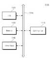
도 19를 참조하면, 본 발명의 실시예에 따른 전자 시스템(1100)은 컨트롤러(1110, controller), 입출력 장치(1120, I/O), 기억 장치(1130, memory device), 인터페이스(1140) 및 버스(1150, bus)를 포함할 수 있다. 컨트롤러(1110), 입출력 장치(1120), 기억 장치(1130) 및/또는 인터페이스(1140)는 버스(1150)를 통하여 서로 결합 될 수 있다. 버스(1150)는 데이터들이 이동되는 통로(path)에 해당한다.Referring to Figure 19, an
컨트롤러(1110)는 마이크로프로세서, 디지털 신호 프로세스, 마이크로 컨트롤러, 및 이들과 유사한 기능을 수행할 수 있는 논리 소자들 중에서 적어도 하나를 포함할 수 있다. 입출력 장치(1120)는 키패드(keypad), 키보드 및 디스플레이 장치 등을 포함할 수 있다. 기억 장치(1130)는 데이터 및/또는 명령어 등을 저장할 수 있다. 인터페이스(1140)는 통신 네트워크로 데이터를 전송하거나 통신 네트워크로부터 데이터를 수신하는 기능을 수행할 수 있다. 인터페이스(1140)는 유선 또는 무선 형태일 수 있다. 예컨대, 인터페이스(1140)는 안테나 또는 유무선 트랜시버 등을 포함할 수 있다. 도시하지 않았지만, 전자 시스템(1100)은 컨트롤러(1110)의 동작을 향상시키기 위한 동작 메모리로서, 고속의 디램 및/또는 에스램등을 더 포함할 수도 있다. 본 발명의 실시예들에 따른 반도체 소자는 기억 장치(1130) 내에 제공되거나, 컨트롤러(1110), 입출력 장치(1120, I/O) 등의 일부로 제공될 수 있다.The
전자 시스템(1100)은 개인 휴대용 정보 단말기(PDA, personal digital aSSistant) 포터블 컴퓨터(portable computer), 웹 타블렛(web tablet), 무선 전화기(wireleSS phone), 모바일 폰(mobile phone), 디지털 뮤직 플레이어(digital music player), 메모리 카드(memory card), 또는 정보를 무선환경에서 송신 및/또는 수신할 수 있는 모든 전자 제품에 적용될 수 있다.
도 20은 본 발명의 실시예들에 따른 반도체 소자를 포함하는 전자 장치의 구성을 보여주는 블록도이다.20 is a block diagram showing the configuration of an electronic device including a semiconductor device according to embodiments of the present invention.
도 20을 참조하면, 전자 장치(1200)는 반도체 칩(1200)을 포함할 수 있다. 반도체 칩(1200)은 프로세서(Processor; 1201), 임베디드 메모리(Embedded Memory; 1203) 및 캐시 메모리(Cache Memory; 1205)를 포함할 수 있다.Referring to FIG. 20, the
프로세서(1201)는 하나 이상의 프로세서 코어들(Processor Core; C1-Cn)을 포함할 수 있다. 하나 이상의 프로세서 코어들(C1-Cn)은 데이터 및 신호를 처리할 수 있다. 프로세서 코어들(C1-Cn)은 본 발명의 실시예들에 따른 반도체 소자를 포함할 수 있다.The processor 1201 may include one or more processor cores (C1-Cn). One or more processor cores (C1-Cn) may process data and signals. The processor cores C1-Cn may comprise semiconductor devices according to embodiments of the present invention.
전자 장치(1200)는 처리된 데이터 및 신호를 이용하여 고유의 기능을 수행할 수 있다. 일 예로, 프로세서(1201)는 어플리케이션 프로세서(Application Processor)일 수 있다.The
임베디드 메모리(1203)는 프로세서(1201)와 제1 데이터(DAT1)를 교환할 수 있다. 제1 데이터(DAT1)는 하나 이상의 프로세서 코어들(C1-Cn)에 의해 처리된 또는 처리될 데이터이다. 임베디드 메모리(1203)는 제1 데이터(DAT1)를 관리할 수 있다. 예를 들어, 임베디드 메모리(1203)는 제1 데이터(DAT1)를 버퍼링(Buffering)할 수 있다. 즉, 임베디드 메모리(1203)는 프로세서(1201)의 버퍼 메모리 또는 워킹 메모리(Working Memory)로서 작동할 수 있다.The embedded memory 1203 can exchange the first data DAT1 with the processor 1201. [ The first data DAT1 is data to be processed or processed by one or more processor cores C1-Cn. The embedded memory 1203 can manage the first data DAT1. For example, the embedded memory 1203 may buffer the first data DAT1. That is, the embedded memory 1203 may operate as a buffer memory or a working memory of the processor 1201.
일 실시예에 따르면, 전자 장치(1200)는 웨어러블(Wearable) 전자 장치에 적용될 수 있다. 웨어러블 전자 장치는 많은 양의 연산을 필요로 하는 기능보다 적은 양의 연산을 필요로 하는 기능을 더 많이 수행할 수 있다. 따라서, 전자 장치(1200)가 웨어러블 전자 장치에 적용될 경우, 임베디드 메모리(1203)는 큰 버퍼 용량을 갖지 않아도 무방할 수 있다.According to one embodiment, the
임베디드 메모리(1203)는 SRAM일 수 있다. SRAM은 DRAM 보다 빠른 속도로 작동할 수 있다. SRAM이 반도체 칩(1200)에 임베디드되면, 작은 크기를 갖고 빠른 속도로 작동하는 전자 장치(1200)가 구현될 수 있다. 나아가, SRAM이 반도체 칩(1200)에 임베디드되면, 전자 장치(1200)의 작동 전력(Active Power)의 소모량이 감소할 수 있다. SRAM은 본 발명의 실시예들에 따른 반도체 소자를 포함할 수 있다.The embedded memory 1203 may be an SRAM. SRAM can operate faster than DRAM. When the SRAM is embedded in the
캐시 메모리(1205)는 하나 이상의 프로세서 코어들(C1 내지 Cn)과 함께 반도체 칩(1200) 위에 실장될 수 있다. 캐시 메모리(1205)는 캐시 데이터(DATc)를 저장할 수 있다. 캐시 데이터(DATc)는 하나 이상의 프로세서 코어들(C1 내지 Cn)에 의해 이용되는 데이터일 수 있다. 캐시 메모리(1205)는 적은 저장 용량을 갖지만, 매우 빠른 속도로 작동할 수 있다. 일 예로, 캐시 메모리(1205)는 본 발명의 실시예들에 따른 반도체 소자를 포함하는 SRAM(Static Random Access Memory)을 포함할 수 있다. 캐시 메모리(1205)는 본 발명의 실시예들에 따른 반도체 소자를 포함하는 SRAM(Static Random Access Memory)을 포함할 수 있다. 캐시 메모리(1205)가 이용되는 경우, 프로세서(1201)가 임베디드 메모리(1203)에 접근하는 횟수 및 시간이 감소할 수 있다. 따라서, 캐시 메모리(1205)가 이용되는 경우, 전자 장치(1200)의 작동 속도가 빨라질 수 있다.The cache memory 1205 may be mounted on the
이해를 돕기 위해, 도 20에서, 캐시 메모리(1205)는 프로세서(1201)와 별개의 구성 요소로 도시되었다. 그러나, 캐시 메모리(1205)는 프로세서(1201)에 포함되도록 구성될 수 있다. 도 20은 본 발명의 기술 사상의 보호 범위를 제한하기 위한 것은 아니다.For ease of understanding, in FIG. 20, cache memory 1205 is shown as a separate component from processor 1201. However, the cache memory 1205 may be configured to be included in the processor 1201. 20 is not intended to limit the scope of protection of the technical idea of the present invention.
프로세서(1201), 임베디드 메모리(1203) 및 캐시 메모리(1205)는 다양한 인터페이스 규약에 기초하여 데이터를 전송할 수 있다. 예컨대, 프로세서(1201), 임베디드 메모리(1203) 및 캐시 메모리(1205)는 USB(Universal Serial Bus), SCSI(Small Computer System Interface), PCI(Peripheral Component Interconnect) Express, ATA(Advanced Technology Attachment), PATA(Parallel ATA), SATA(Serial ATA), SAS(Serial Attached SCSI), IDE(Integrated Drive Electronics), UFS(Universal Flash Storage) 등 중에서 하나 이상의 인터페이스 규약에 기초하여 데이터를 전송할 수 있다.The processor 1201, the embedded memory 1203, and the cache memory 1205 can transfer data based on various interface conventions. For example, the processor 1201, the embedded memory 1203, and the cache memory 1205 may be connected to a computer system such as a Universal Serial Bus (USB), a Small Computer System Interface (SCSI), a Peripheral Component Interconnect (PCI) Express, an Advanced Technology Attachment (ATA) Data can be transferred based on one or more of interface conventions, such as Parallel ATA, Serial ATA, Serial Attached SCSI (SAS), Integrated Drive Electronics (IDE), Universal Flash Storage (UFS)
전자 시스템(도 19의 1100)은 다양한 전자기기들의 전자 제어 장치에 적용될 수 있다. 도 21은 전자 시스템(도 19의 1100)이 모바일 폰(2000)에 적용되는 예를 도시한다. 그 밖에, 전자 시스템(도 19의 1100)은 휴대용 노트북, MP3 플레이어, 네비게이션(Navigation), 고상 디스크(Solid state disk; SSD), 자동차 또는 가전 제품(Household appliances)에 적용될 수 있다.The electronic system (1100 in Fig. 19) can be applied to electronic control devices of various electronic devices. Fig. 21 shows an example in which the electronic system (1100 in Fig. 19) is applied to the
이상, 첨부된 도면을 참조하여 본 발명의 실시예를 설명하였지만, 본 발명이 속하는 기술분야에서 통상의 지식을 가진 자는 본 발명이 그 기술적 사상이나 필수적인 특징을 변경하지 않고서 다른 구체적인 형태로 실시될 수 있다는 것을 이해할 수 있을 것이다. 그러므로 이상에서 기술한 실시예에는 모든 면에서 예시적인 것이며 한정적이 아닌 것으로 이해해야만 한다.While the present invention has been described in connection with what is presently considered to be practical exemplary embodiments, it is to be understood that the invention is not limited to the disclosed embodiments, but, on the contrary, It will be understood. It is therefore to be understood that the above-described embodiments are illustrative and not restrictive in every respect.
Claims (10)
Translated fromKorean상기 제1 방향과 교차하는 제2 방향으로 연장되어 상기 핀 구조체를 가로지르는 희생 게이트 패턴을 형성하는 것;
상기 핀 구조체 및 상기 희생 게이트 패턴을 덮는 게이트 스페이서막을 형성하는 것;
상기 기판 상에, 제1 입사각 범위를 가지고 조사되는 제1 이온 빔, 및 제2 입사각 범위를 가지고 조사되는 제2 이온 빔을 제공하는 것, 상기 제1 및 2 이온 빔들은 동시에 조사되고;
상기 제1 이온 빔 및 상기 제2 이온 빔을 이용하여 상기 게이트 스페이서막을 패터닝하여, 상기 희생 게이트 패턴의 측벽들 상에 게이트 스페이서들을 형성하는 것;
상기 희생 게이트 패턴의 양 측에 소스/드레인 영역들을 형성하는 것; 및
상기 희생 게이트 패턴을 게이트 전극으로 교체하는 것을 포함하고,
평면적 관점에서, 상기 제1 이온 빔은 상기 제2 방향을 따라 조사되고, 상기 제2 이온 빔은 상기 제2 방향의 반대 방향을 따라 조사되는 반도체 소자의 제조 방법.Forming a pin structure extending in a first direction on the substrate;
Forming a sacrificial gate pattern extending in a second direction that intersects the first direction and traversing the pin structure;
Forming a gate spacer film covering the pin structure and the sacrificial gate pattern;
Providing on the substrate a first ion beam irradiated with a first incident angle range and a second ion beam irradiated with a second incident angle range, the first and second ion beams being simultaneously irradiated;
Patterning the gate spacer film using the first ion beam and the second ion beam to form gate spacers on sidewalls of the sacrificial gate pattern;
Forming source / drain regions on both sides of the sacrificial gate pattern; And
And replacing the sacrificial gate pattern with a gate electrode,
From a plan viewpoint, the first ion beam is irradiated along the second direction, and the second ion beam is irradiated along the opposite direction of the second direction.
상기 제1 입사각의 범위 및 제2 입사각의 범위의 각각은 10 내지 50도 이되,
상기 제1 입사각의 범위 및 상기 제2 입사각의 범위는 상기 기판의 상면에 수직인 법선에 대해 기울어진 각도의 범위로 정의되는 반도체 소자의 제조 방법.The method according to claim 1,
Wherein each of the range of the first incident angle and the range of the second incident angle is 10 to 50 degrees,
Wherein the range of the first angle of incidence and the range of the second angle of incidence are defined as ranges of angles inclined with respect to a normal perpendicular to the upper surface of the substrate.
상기 제1 이온 빔 및 상기 제2 이온 빔을 제공하는 것은:
상기 기판 상에 소스 가스를 공급하는 것;
플라즈마 파워를 이용하여 상기 소스 가스를 플라즈마로 변환시키는 것; 및
상기 기판에 이온 추출 전압을 인가하여, 상기 플라즈마로부터 상기 제1 이온 빔 및 상기 제2 이온 빔을 추출하는 것을 포함하는 반도체 소자의 제조 방법.The method according to claim 1,
Providing the first ion beam and the second ion beam comprises:
Supplying a source gas onto the substrate;
Converting the source gas to plasma using plasma power; And
And applying an ion extraction voltage to the substrate to extract the first ion beam and the second ion beam from the plasma.
상기 소스 가스는 플로린 계열의 식각 가스와 산소 가스의 혼합 가스를 포함하는 반도체 소자의 제조 방법.The method of claim 3,
Wherein the source gas comprises a mixed gas of an etching gas and a fluorine series gas.
상기 플로린 계열의 식각 가스는 CH3F, CF4, C2F6, SiF4 또는 NF3 를 포함하는 반도체 소자의 제조 방법.5. The method of claim 4,
Wherein the fluorine-based etching gas includes CH3F, CF4, C2F6, SiF4, or NF3.
상기 소스 가스 내의 상기 산소 가스의 분압 비율은 50 내지 80%인 반도체 소자의 제조 방법.6. The method of claim 5,
Wherein a partial pressure ratio of the oxygen gas in the source gas is 50 to 80%.
상기 이온 추출 전압은 펄스 형태로 인가되고,
상기 이온 추출 전압의 듀티 사이클(duty cycle)은 50 내지 75% 인 반도체 소자의 제조 방법.The method of claim 3,
The ion extraction voltage is applied in the form of a pulse,
Wherein the duty cycle of the ion extraction voltage is 50 to 75%.
상기 핀 구조체는 상기 희생 게이트 패턴 아래의 제1 부분, 및 상기 희생 게이트 양 측의 제2 부분들을 포함하고,
상기 게이트 스페이서막은 상기 제2 부분들의 상면 및 측벽들을 덮고,
상기 게이트 스페이서막을 패터닝 하는 것은, 상기 제1 이온 빔 및 상기 제2 이온 빔을 이용하여 상기 제2 부분들 각각의 상기 상면 및 상기 측벽들 상의 상기 게이트 스페이서막을 전부 제거하는 포함하되,
상기 측벽들은 상기 제2 방향으로 서로 마주하는 반도체 소자의 제조 방법.The method according to claim 1,
Wherein the pin structure includes a first portion under the sacrificial gate pattern and second portions on both sides of the sacrificial gate,
The gate spacer film covers the top and sidewalls of the second portions,
Wherein patterning the gate spacer film comprises removing all of the gate spacer film on the top and sidewalls of each of the second portions using the first ion beam and the second ion beam,
And the sidewalls face each other in the second direction.
상기 소스/드레인 영역들을 형성하는 것은, 에피택시얼 공정을 수행하여 상기 제2 부분들 상에 클래딩층들을 형성하는 것을 포함하되,
상기 클래딩층들 각각은:
상기 기판의 상면에 대해 실질적으로 네거티브하게 경사진 제1 측벽;
상기 기판의 상기 상면에 대해 실직적으로 포지티브하게 경사진 제2 측벽; 및
상기 제1 및 제2 측벽들과 연결되는 제3 측벽을 포함하되,
상기 기판에 인접한 상기 제3 측벽의 일단은 상기 제1 측벽의 일단과 연결되고, 상기 제3 측벽의 타단은 상기 제2 측벽의 일단과 연결되는 반도체 소자의 제조 방법.9. The method of claim 8,
Forming the source / drain regions comprises: performing an epitaxial process to form cladding layers on the second portions,
Wherein each of the cladding layers comprises:
A first side wall inclined substantially negatively with respect to an upper surface of the substrate;
A second side wall that is inclined substantially positively with respect to the upper surface of the substrate; And
And a third sidewall connected to the first and second sidewalls,
Wherein one end of the third sidewall adjacent to the substrate is connected to one end of the first sidewall and the other end of the third sidewall is connected to one end of the second sidewall.
상기 소스 드레인 영역들을 형성하는 것은,
상기 클레딩츨들의 형성 전에, 상기 제2 부분들의 일부를 불순물로 도핑하는 것을 더 포함하는 반도체 소자의 제조 방법.10. The method of claim 9,
Forming source and drain regions,
Further comprising doping a portion of the second portions with an impurity before formation of the clamping dots.
Priority Applications (2)
| Application Number | Priority Date | Filing Date | Title |
|---|---|---|---|
| KR1020150079338AKR20160143942A (en) | 2015-06-04 | 2015-06-04 | Method of manufacturing semiconductor device |
| US15/131,611US9793381B2 (en) | 2015-06-04 | 2016-04-18 | Method for manufacturing a semiconductor device |
Applications Claiming Priority (1)
| Application Number | Priority Date | Filing Date | Title |
|---|---|---|---|
| KR1020150079338AKR20160143942A (en) | 2015-06-04 | 2015-06-04 | Method of manufacturing semiconductor device |
Publications (1)
| Publication Number | Publication Date |
|---|---|
| KR20160143942Atrue KR20160143942A (en) | 2016-12-15 |
Family
ID=57452631
Family Applications (1)
| Application Number | Title | Priority Date | Filing Date |
|---|---|---|---|
| KR1020150079338ACeasedKR20160143942A (en) | 2015-06-04 | 2015-06-04 | Method of manufacturing semiconductor device |
Country Status (2)
| Country | Link |
|---|---|
| US (1) | US9793381B2 (en) |
| KR (1) | KR20160143942A (en) |
Families Citing this family (6)
| Publication number | Priority date | Publication date | Assignee | Title |
|---|---|---|---|---|
| US11437516B2 (en)* | 2016-11-28 | 2022-09-06 | Taiwan Semiconductor Manufacturing Co., Ltd. | Mechanisms for growing epitaxy structure of finFET device |
| CN109524302B (en)* | 2017-09-20 | 2020-12-15 | 华邦电子股份有限公司 | Semiconductor component and method of manufacturing the same |
| US10068902B1 (en)* | 2017-09-26 | 2018-09-04 | Globalfoundries Inc. | Integrated circuit structure incorporating non-planar field effect transistors with different channel region heights and method |
| US10510870B2 (en)* | 2018-02-21 | 2019-12-17 | Varian Semiconductor Equipment Associates, Inc. | Techniques for forming device having etch-resistant isolation oxide |
| US10950434B2 (en)* | 2018-06-27 | 2021-03-16 | Taiwan Semiconductor Manufacturing Co., Ltd. | Methods of reducing gate spacer loss during semiconductor manufacturing |
| GB2582242A (en)* | 2018-11-30 | 2020-09-23 | Oxford Instruments Nanotechnology Tools Ltd | Charged particle beam source, surface processing apparatus and surface processing method |
Family Cites Families (28)
| Publication number | Priority date | Publication date | Assignee | Title |
|---|---|---|---|---|
| KR100485387B1 (en)* | 2002-11-26 | 2005-04-27 | 삼성전자주식회사 | Method for monitoring an ion implanter and ion implanter having a shadow jig for performing the same |
| JP2005294789A (en)* | 2004-03-10 | 2005-10-20 | Toshiba Corp | Semiconductor device and manufacturing method thereof |
| JP2007073831A (en) | 2005-09-08 | 2007-03-22 | Toshiba Corp | Manufacturing method of semiconductor device |
| US7452766B2 (en) | 2006-08-31 | 2008-11-18 | Micron Technology, Inc. | Finned memory cells and the fabrication thereof |
| US8518767B2 (en) | 2007-02-28 | 2013-08-27 | International Business Machines Corporation | FinFET with reduced gate to fin overlay sensitivity |
| US7667271B2 (en)* | 2007-04-27 | 2010-02-23 | Taiwan Semiconductor Manufacturing Company, Ltd. | Fin field-effect transistors |
| US7872303B2 (en) | 2008-08-14 | 2011-01-18 | International Business Machines Corporation | FinFET with longitudinal stress in a channel |
| US8124507B2 (en)* | 2009-06-24 | 2012-02-28 | Panasonic Corporation | Semiconductor device and method for fabricating the same |
| US8716797B2 (en) | 2009-11-03 | 2014-05-06 | International Business Machines Corporation | FinFET spacer formation by oriented implantation |
| US9312179B2 (en) | 2010-03-17 | 2016-04-12 | Taiwan-Semiconductor Manufacturing Co., Ltd. | Method of making a finFET, and finFET formed by the method |
| US8486769B2 (en) | 2010-11-19 | 2013-07-16 | Taiwan Semiconductor Manufacturing Company, Ltd. | Method for forming metrology structures from fins in integrated circuitry |
| US8633076B2 (en) | 2010-11-23 | 2014-01-21 | Taiwan Semiconductor Manufacturing Company, Ltd. | Method for adjusting fin width in integrated circuitry |
| US8383485B2 (en) | 2011-07-13 | 2013-02-26 | Taiwan Semiconductor Manufacturing Co., Ltd. | Epitaxial process for forming semiconductor devices |
| KR101894221B1 (en)* | 2012-03-21 | 2018-10-04 | 삼성전자주식회사 | Field effect transistor and semiconductor device including the same |
| WO2013154842A1 (en) | 2012-04-11 | 2013-10-17 | Tokyo Electron Limited | Aspect ratio dependent deposition to improve gate spacer profile, fin-loss and hardmask-loss for finfet scheme |
| US9142633B2 (en) | 2012-12-13 | 2015-09-22 | GlobalFoundries, Inc. | Integrated circuits and methods for fabricating integrated circuits with silicide contacts on non-planar structures |
| US8815691B2 (en) | 2012-12-21 | 2014-08-26 | Taiwan Semiconductor Manufacturing Company, Ltd. | Method of fabricating a gate all around device |
| US8921191B2 (en) | 2013-02-05 | 2014-12-30 | GlobalFoundries, Inc. | Integrated circuits including FINFET devices with lower contact resistance and reduced parasitic capacitance and methods for fabricating the same |
| US9831345B2 (en) | 2013-03-11 | 2017-11-28 | Taiwan Semiconductor Manufacturing Company, Ltd. | FinFET with rounded source/drain profile |
| US8796093B1 (en) | 2013-03-14 | 2014-08-05 | International Business Machines Corporation | Doping of FinFET structures |
| KR102055379B1 (en)* | 2013-08-08 | 2019-12-13 | 삼성전자 주식회사 | Semiconductor device having tri-gate and manufacturing method thereof |
| KR102175854B1 (en)* | 2013-11-14 | 2020-11-09 | 삼성전자주식회사 | Semiconductor device and method of manufacturing the same |
| US9548213B2 (en)* | 2014-02-25 | 2017-01-17 | International Business Machines Corporation | Dielectric isolated fin with improved fin profile |
| KR102212267B1 (en)* | 2014-03-19 | 2021-02-04 | 삼성전자주식회사 | Semiconductor device and method for fabricating the same |
| KR102017611B1 (en)* | 2014-04-04 | 2019-09-04 | 삼성전자주식회사 | Semiconductor device and method of manufacturing the same |
| CN105470132B (en)* | 2014-09-03 | 2018-08-10 | 中芯国际集成电路制造(上海)有限公司 | The forming method of fin field effect pipe |
| KR102265956B1 (en)* | 2014-09-29 | 2021-06-17 | 삼성전자주식회사 | Semiconductor devices having a source/drain and Method for fabricating the same |
| US9484461B2 (en)* | 2014-09-29 | 2016-11-01 | Taiwan Semiconductor Manufacturing Company, Ltd. | Integrated circuit structure with substrate isolation and un-doped channel |
- 2015
- 2015-06-04KRKR1020150079338Apatent/KR20160143942A/ennot_activeCeased
- 2016
- 2016-04-18USUS15/131,611patent/US9793381B2/ennot_activeExpired - Fee Related
Also Published As
| Publication number | Publication date |
|---|---|
| US20160359020A1 (en) | 2016-12-08 |
| US9793381B2 (en) | 2017-10-17 |
Similar Documents
| Publication | Publication Date | Title |
|---|---|---|
| CN106128958B (en) | Method for manufacturing semiconductor device | |
| US9935017B2 (en) | Methods of manufacturing semiconductor devices by forming source/drain regions before gate electrode separation | |
| CN106024868B (en) | semiconductor device | |
| CN113707658B (en) | Semiconductor device and method of manufacturing the same | |
| US9960241B2 (en) | Semiconductor device for manufacturing | |
| KR102170701B1 (en) | Semiconductor device and method of fabricating the same | |
| KR102290538B1 (en) | Semiconductor device and method for manufacturing the same | |
| US9536881B2 (en) | Semiconductor devices having fin shaped channels | |
| US20150035061A1 (en) | Semiconductor Device and Method for Fabricating the Same | |
| KR102395073B1 (en) | Semiconductor device | |
| US9536950B2 (en) | Semiconductor device and method of fabricating the same | |
| KR102050214B1 (en) | Method for fabricating semiconductor device | |
| US20160086841A1 (en) | Method for forming pattern of semiconductor device and semiconductor device formed using the same | |
| KR20160143942A (en) | Method of manufacturing semiconductor device | |
| KR20160122909A (en) | Semiconductor device and method for manufacturing the same | |
| KR20140088419A (en) | Field effect transistor | |
| US9466703B2 (en) | Method for fabricating semiconductor device | |
| US20160307767A1 (en) | Semiconductor device and method of fabricating the same | |
| KR102307207B1 (en) | Semiconductor devices including field effect transistors | |
| KR102354473B1 (en) | Semiconductor device and method for manufacturing the same | |
| KR20160135010A (en) | Semiconductor devices including field effect transistors | |
| US20160322495A1 (en) | Semiconductor device and method of manufacturing the same | |
| KR20160121682A (en) | Semiconductor dievices and methods of manufacturing the same |
Legal Events
| Date | Code | Title | Description |
|---|---|---|---|
| PA0109 | Patent application | Patent event code:PA01091R01D Comment text:Patent Application Patent event date:20150604 | |
| PG1501 | Laying open of application | ||
| A201 | Request for examination | ||
| PA0201 | Request for examination | Patent event code:PA02012R01D Patent event date:20200526 Comment text:Request for Examination of Application Patent event code:PA02011R01I Patent event date:20150604 Comment text:Patent Application | |
| E902 | Notification of reason for refusal | ||
| PE0902 | Notice of grounds for rejection | Comment text:Notification of reason for refusal Patent event date:20211019 Patent event code:PE09021S01D | |
| E601 | Decision to refuse application | ||
| PE0601 | Decision on rejection of patent | Patent event date:20220103 Comment text:Decision to Refuse Application Patent event code:PE06012S01D Patent event date:20211019 Comment text:Notification of reason for refusal Patent event code:PE06011S01I |