KR20160143614A - Semiconductor device - Google Patents
Semiconductor deviceDownload PDFInfo
- Publication number
- KR20160143614A KR20160143614AKR1020160162494AKR20160162494AKR20160143614AKR 20160143614 AKR20160143614 AKR 20160143614AKR 1020160162494 AKR1020160162494 AKR 1020160162494AKR 20160162494 AKR20160162494 AKR 20160162494AKR 20160143614 AKR20160143614 AKR 20160143614A
- Authority
- KR
- South Korea
- Prior art keywords
- layer
- oxide semiconductor
- film
- thin film
- semiconductor layer
- Prior art date
- Legal status (The legal status is an assumption and is not a legal conclusion. Google has not performed a legal analysis and makes no representation as to the accuracy of the status listed.)
- Granted
Links
Images


Classifications
- H—ELECTRICITY
- H10—SEMICONDUCTOR DEVICES; ELECTRIC SOLID-STATE DEVICES NOT OTHERWISE PROVIDED FOR
- H10D—INORGANIC ELECTRIC SEMICONDUCTOR DEVICES
- H10D30/00—Field-effect transistors [FET]
- H10D30/60—Insulated-gate field-effect transistors [IGFET]
- H10D30/67—Thin-film transistors [TFT]
- H10D30/6757—Thin-film transistors [TFT] characterised by the structure of the channel, e.g. transverse or longitudinal shape or doping profile
- H01L29/7869—
- H—ELECTRICITY
- H10—SEMICONDUCTOR DEVICES; ELECTRIC SOLID-STATE DEVICES NOT OTHERWISE PROVIDED FOR
- H10D—INORGANIC ELECTRIC SEMICONDUCTOR DEVICES
- H10D30/00—Field-effect transistors [FET]
- H10D30/60—Insulated-gate field-effect transistors [IGFET]
- H10D30/67—Thin-film transistors [TFT]
- H10D30/674—Thin-film transistors [TFT] characterised by the active materials
- H10D30/6755—Oxide semiconductors, e.g. zinc oxide, copper aluminium oxide or cadmium stannate
- H—ELECTRICITY
- H01—ELECTRIC ELEMENTS
- H01L—SEMICONDUCTOR DEVICES NOT COVERED BY CLASS H10
- H01L21/00—Processes or apparatus adapted for the manufacture or treatment of semiconductor or solid state devices or of parts thereof
- H01L21/02—Manufacture or treatment of semiconductor devices or of parts thereof
- H01L21/02104—Forming layers
- H01L21/02107—Forming insulating materials on a substrate
- H01L21/02109—Forming insulating materials on a substrate characterised by the type of layer, e.g. type of material, porous/non-porous, pre-cursors, mixtures or laminates
- H01L21/02112—Forming insulating materials on a substrate characterised by the type of layer, e.g. type of material, porous/non-porous, pre-cursors, mixtures or laminates characterised by the material of the layer
- H01L21/02123—Forming insulating materials on a substrate characterised by the type of layer, e.g. type of material, porous/non-porous, pre-cursors, mixtures or laminates characterised by the material of the layer the material containing silicon
- H01L21/02164—Forming insulating materials on a substrate characterised by the type of layer, e.g. type of material, porous/non-porous, pre-cursors, mixtures or laminates characterised by the material of the layer the material containing silicon the material being a silicon oxide, e.g. SiO2
- H—ELECTRICITY
- H01—ELECTRIC ELEMENTS
- H01L—SEMICONDUCTOR DEVICES NOT COVERED BY CLASS H10
- H01L21/00—Processes or apparatus adapted for the manufacture or treatment of semiconductor or solid state devices or of parts thereof
- H01L21/02—Manufacture or treatment of semiconductor devices or of parts thereof
- H01L21/02104—Forming layers
- H01L21/02107—Forming insulating materials on a substrate
- H01L21/02296—Forming insulating materials on a substrate characterised by the treatment performed before or after the formation of the layer
- H01L21/02318—Forming insulating materials on a substrate characterised by the treatment performed before or after the formation of the layer post-treatment
- H01L21/02321—Forming insulating materials on a substrate characterised by the treatment performed before or after the formation of the layer post-treatment introduction of substances into an already existing insulating layer
- H01L21/02323—Forming insulating materials on a substrate characterised by the treatment performed before or after the formation of the layer post-treatment introduction of substances into an already existing insulating layer introduction of oxygen
- H—ELECTRICITY
- H01—ELECTRIC ELEMENTS
- H01L—SEMICONDUCTOR DEVICES NOT COVERED BY CLASS H10
- H01L21/00—Processes or apparatus adapted for the manufacture or treatment of semiconductor or solid state devices or of parts thereof
- H01L21/02—Manufacture or treatment of semiconductor devices or of parts thereof
- H01L21/02104—Forming layers
- H01L21/02365—Forming inorganic semiconducting materials on a substrate
- H01L21/02518—Deposited layers
- H01L21/02521—Materials
- H01L21/02565—Oxide semiconducting materials not being Group 12/16 materials, e.g. ternary compounds
- H—ELECTRICITY
- H01—ELECTRIC ELEMENTS
- H01L—SEMICONDUCTOR DEVICES NOT COVERED BY CLASS H10
- H01L21/00—Processes or apparatus adapted for the manufacture or treatment of semiconductor or solid state devices or of parts thereof
- H01L21/02—Manufacture or treatment of semiconductor devices or of parts thereof
- H01L21/04—Manufacture or treatment of semiconductor devices or of parts thereof the devices having potential barriers, e.g. a PN junction, depletion layer or carrier concentration layer
- H01L21/18—Manufacture or treatment of semiconductor devices or of parts thereof the devices having potential barriers, e.g. a PN junction, depletion layer or carrier concentration layer the devices having semiconductor bodies comprising elements of Group IV of the Periodic Table or AIIIBV compounds with or without impurities, e.g. doping materials
- H01L21/30—Treatment of semiconductor bodies using processes or apparatus not provided for in groups H01L21/20 - H01L21/26
- H01L21/31—Treatment of semiconductor bodies using processes or apparatus not provided for in groups H01L21/20 - H01L21/26 to form insulating layers thereon, e.g. for masking or by using photolithographic techniques; After treatment of these layers; Selection of materials for these layers
- H01L21/3205—Deposition of non-insulating-, e.g. conductive- or resistive-, layers on insulating layers; After-treatment of these layers
- H01L21/321—After treatment
- H01L21/3213—Physical or chemical etching of the layers, e.g. to produce a patterned layer from a pre-deposited extensive layer
- H01L21/32139—Physical or chemical etching of the layers, e.g. to produce a patterned layer from a pre-deposited extensive layer using masks
- H—ELECTRICITY
- H01—ELECTRIC ELEMENTS
- H01L—SEMICONDUCTOR DEVICES NOT COVERED BY CLASS H10
- H01L21/00—Processes or apparatus adapted for the manufacture or treatment of semiconductor or solid state devices or of parts thereof
- H01L21/02—Manufacture or treatment of semiconductor devices or of parts thereof
- H01L21/04—Manufacture or treatment of semiconductor devices or of parts thereof the devices having potential barriers, e.g. a PN junction, depletion layer or carrier concentration layer
- H01L21/34—Manufacture or treatment of semiconductor devices or of parts thereof the devices having potential barriers, e.g. a PN junction, depletion layer or carrier concentration layer the devices having semiconductor bodies not provided for in groups H01L21/18, H10D48/04 and H10D48/07, with or without impurities, e.g. doping materials
- H01L21/46—Treatment of semiconductor bodies using processes or apparatus not provided for in groups H01L21/428
- H01L21/461—Treatment of semiconductor bodies using processes or apparatus not provided for in groups H01L21/428 to change their surface-physical characteristics or shape, e.g. etching, polishing, cutting
- H01L21/465—Chemical or electrical treatment, e.g. electrolytic etching
- H01L21/467—Chemical or electrical treatment, e.g. electrolytic etching using masks
- H—ELECTRICITY
- H01—ELECTRIC ELEMENTS
- H01L—SEMICONDUCTOR DEVICES NOT COVERED BY CLASS H10
- H01L21/00—Processes or apparatus adapted for the manufacture or treatment of semiconductor or solid state devices or of parts thereof
- H01L21/02—Manufacture or treatment of semiconductor devices or of parts thereof
- H01L21/04—Manufacture or treatment of semiconductor devices or of parts thereof the devices having potential barriers, e.g. a PN junction, depletion layer or carrier concentration layer
- H01L21/34—Manufacture or treatment of semiconductor devices or of parts thereof the devices having potential barriers, e.g. a PN junction, depletion layer or carrier concentration layer the devices having semiconductor bodies not provided for in groups H01L21/18, H10D48/04 and H10D48/07, with or without impurities, e.g. doping materials
- H01L21/46—Treatment of semiconductor bodies using processes or apparatus not provided for in groups H01L21/428
- H01L21/461—Treatment of semiconductor bodies using processes or apparatus not provided for in groups H01L21/428 to change their surface-physical characteristics or shape, e.g. etching, polishing, cutting
- H01L21/4763—Deposition of non-insulating, e.g. conductive -, resistive -, layers on insulating layers; After-treatment of these layers
- H01L21/47635—After-treatment of these layers
- H01L27/1225—
- H01L29/263—
- H01L29/45—
- H01L29/66742—
- H01L29/78606—
- H—ELECTRICITY
- H10—SEMICONDUCTOR DEVICES; ELECTRIC SOLID-STATE DEVICES NOT OTHERWISE PROVIDED FOR
- H10D—INORGANIC ELECTRIC SEMICONDUCTOR DEVICES
- H10D30/00—Field-effect transistors [FET]
- H10D30/01—Manufacture or treatment
- H10D30/021—Manufacture or treatment of FETs having insulated gates [IGFET]
- H10D30/031—Manufacture or treatment of FETs having insulated gates [IGFET] of thin-film transistors [TFT]
- H—ELECTRICITY
- H10—SEMICONDUCTOR DEVICES; ELECTRIC SOLID-STATE DEVICES NOT OTHERWISE PROVIDED FOR
- H10D—INORGANIC ELECTRIC SEMICONDUCTOR DEVICES
- H10D30/00—Field-effect transistors [FET]
- H10D30/60—Insulated-gate field-effect transistors [IGFET]
- H10D30/67—Thin-film transistors [TFT]
- H10D30/6704—Thin-film transistors [TFT] having supplementary regions or layers in the thin films or in the insulated bulk substrates for controlling properties of the device
- H10D30/6713—Thin-film transistors [TFT] having supplementary regions or layers in the thin films or in the insulated bulk substrates for controlling properties of the device characterised by the properties of the source or drain regions, e.g. compositions or sectional shapes
- H—ELECTRICITY
- H10—SEMICONDUCTOR DEVICES; ELECTRIC SOLID-STATE DEVICES NOT OTHERWISE PROVIDED FOR
- H10D—INORGANIC ELECTRIC SEMICONDUCTOR DEVICES
- H10D30/00—Field-effect transistors [FET]
- H10D30/60—Insulated-gate field-effect transistors [IGFET]
- H10D30/67—Thin-film transistors [TFT]
- H10D30/6704—Thin-film transistors [TFT] having supplementary regions or layers in the thin films or in the insulated bulk substrates for controlling properties of the device
- H10D30/6723—Thin-film transistors [TFT] having supplementary regions or layers in the thin films or in the insulated bulk substrates for controlling properties of the device having light shields
- H—ELECTRICITY
- H10—SEMICONDUCTOR DEVICES; ELECTRIC SOLID-STATE DEVICES NOT OTHERWISE PROVIDED FOR
- H10D—INORGANIC ELECTRIC SEMICONDUCTOR DEVICES
- H10D30/00—Field-effect transistors [FET]
- H10D30/60—Insulated-gate field-effect transistors [IGFET]
- H10D30/67—Thin-film transistors [TFT]
- H10D30/6729—Thin-film transistors [TFT] characterised by the electrodes
- H10D30/673—Thin-film transistors [TFT] characterised by the electrodes characterised by the shapes, relative sizes or dispositions of the gate electrodes
- H—ELECTRICITY
- H10—SEMICONDUCTOR DEVICES; ELECTRIC SOLID-STATE DEVICES NOT OTHERWISE PROVIDED FOR
- H10D—INORGANIC ELECTRIC SEMICONDUCTOR DEVICES
- H10D30/00—Field-effect transistors [FET]
- H10D30/60—Insulated-gate field-effect transistors [IGFET]
- H10D30/67—Thin-film transistors [TFT]
- H10D30/6729—Thin-film transistors [TFT] characterised by the electrodes
- H10D30/6737—Thin-film transistors [TFT] characterised by the electrodes characterised by the electrode materials
- H10D30/6739—Conductor-insulator-semiconductor electrodes
- H—ELECTRICITY
- H10—SEMICONDUCTOR DEVICES; ELECTRIC SOLID-STATE DEVICES NOT OTHERWISE PROVIDED FOR
- H10D—INORGANIC ELECTRIC SEMICONDUCTOR DEVICES
- H10D30/00—Field-effect transistors [FET]
- H10D30/60—Insulated-gate field-effect transistors [IGFET]
- H10D30/67—Thin-film transistors [TFT]
- H10D30/674—Thin-film transistors [TFT] characterised by the active materials
- H10D30/6755—Oxide semiconductors, e.g. zinc oxide, copper aluminium oxide or cadmium stannate
- H10D30/6756—Amorphous oxide semiconductors
- H—ELECTRICITY
- H10—SEMICONDUCTOR DEVICES; ELECTRIC SOLID-STATE DEVICES NOT OTHERWISE PROVIDED FOR
- H10D—INORGANIC ELECTRIC SEMICONDUCTOR DEVICES
- H10D62/00—Semiconductor bodies, or regions thereof, of devices having potential barriers
- H10D62/10—Shapes, relative sizes or dispositions of the regions of the semiconductor bodies; Shapes of the semiconductor bodies
- H10D62/124—Shapes, relative sizes or dispositions of the regions of semiconductor bodies or of junctions between the regions
- H10D62/126—Top-view geometrical layouts of the regions or the junctions
- H—ELECTRICITY
- H10—SEMICONDUCTOR DEVICES; ELECTRIC SOLID-STATE DEVICES NOT OTHERWISE PROVIDED FOR
- H10D—INORGANIC ELECTRIC SEMICONDUCTOR DEVICES
- H10D62/00—Semiconductor bodies, or regions thereof, of devices having potential barriers
- H10D62/10—Shapes, relative sizes or dispositions of the regions of the semiconductor bodies; Shapes of the semiconductor bodies
- H10D62/17—Semiconductor regions connected to electrodes not carrying current to be rectified, amplified or switched, e.g. channel regions
- H10D62/213—Channel regions of field-effect devices
- H10D62/221—Channel regions of field-effect devices of FETs
- H10D62/235—Channel regions of field-effect devices of FETs of IGFETs
- H—ELECTRICITY
- H10—SEMICONDUCTOR DEVICES; ELECTRIC SOLID-STATE DEVICES NOT OTHERWISE PROVIDED FOR
- H10D—INORGANIC ELECTRIC SEMICONDUCTOR DEVICES
- H10D62/00—Semiconductor bodies, or regions thereof, of devices having potential barriers
- H10D62/40—Crystalline structures
- H10D62/402—Amorphous materials
- H—ELECTRICITY
- H10—SEMICONDUCTOR DEVICES; ELECTRIC SOLID-STATE DEVICES NOT OTHERWISE PROVIDED FOR
- H10D—INORGANIC ELECTRIC SEMICONDUCTOR DEVICES
- H10D62/00—Semiconductor bodies, or regions thereof, of devices having potential barriers
- H10D62/80—Semiconductor bodies, or regions thereof, of devices having potential barriers characterised by the materials
- H—ELECTRICITY
- H10—SEMICONDUCTOR DEVICES; ELECTRIC SOLID-STATE DEVICES NOT OTHERWISE PROVIDED FOR
- H10D—INORGANIC ELECTRIC SEMICONDUCTOR DEVICES
- H10D64/00—Electrodes of devices having potential barriers
- H10D64/20—Electrodes characterised by their shapes, relative sizes or dispositions
- H10D64/27—Electrodes not carrying the current to be rectified, amplified, oscillated or switched, e.g. gates
- H10D64/311—Gate electrodes for field-effect devices
- H10D64/411—Gate electrodes for field-effect devices for FETs
- H10D64/511—Gate electrodes for field-effect devices for FETs for IGFETs
- H10D64/514—Gate electrodes for field-effect devices for FETs for IGFETs characterised by the insulating layers
- H—ELECTRICITY
- H10—SEMICONDUCTOR DEVICES; ELECTRIC SOLID-STATE DEVICES NOT OTHERWISE PROVIDED FOR
- H10D—INORGANIC ELECTRIC SEMICONDUCTOR DEVICES
- H10D64/00—Electrodes of devices having potential barriers
- H10D64/60—Electrodes characterised by their materials
- H10D64/62—Electrodes ohmically coupled to a semiconductor
- H—ELECTRICITY
- H10—SEMICONDUCTOR DEVICES; ELECTRIC SOLID-STATE DEVICES NOT OTHERWISE PROVIDED FOR
- H10D—INORGANIC ELECTRIC SEMICONDUCTOR DEVICES
- H10D64/00—Electrodes of devices having potential barriers
- H10D64/60—Electrodes characterised by their materials
- H10D64/66—Electrodes having a conductor capacitively coupled to a semiconductor by an insulator, e.g. MIS electrodes
- H10D64/665—Electrodes having a conductor capacitively coupled to a semiconductor by an insulator, e.g. MIS electrodes the conductor comprising a layer of elemental metal contacting the insulator, e.g. tungsten or molybdenum
- H—ELECTRICITY
- H10—SEMICONDUCTOR DEVICES; ELECTRIC SOLID-STATE DEVICES NOT OTHERWISE PROVIDED FOR
- H10D—INORGANIC ELECTRIC SEMICONDUCTOR DEVICES
- H10D64/00—Electrodes of devices having potential barriers
- H10D64/60—Electrodes characterised by their materials
- H10D64/66—Electrodes having a conductor capacitively coupled to a semiconductor by an insulator, e.g. MIS electrodes
- H10D64/68—Electrodes having a conductor capacitively coupled to a semiconductor by an insulator, e.g. MIS electrodes characterised by the insulator, e.g. by the gate insulator
- H10D64/681—Electrodes having a conductor capacitively coupled to a semiconductor by an insulator, e.g. MIS electrodes characterised by the insulator, e.g. by the gate insulator having a compositional variation, e.g. multilayered
- H10D64/685—Electrodes having a conductor capacitively coupled to a semiconductor by an insulator, e.g. MIS electrodes characterised by the insulator, e.g. by the gate insulator having a compositional variation, e.g. multilayered being perpendicular to the channel plane
- H—ELECTRICITY
- H10—SEMICONDUCTOR DEVICES; ELECTRIC SOLID-STATE DEVICES NOT OTHERWISE PROVIDED FOR
- H10D—INORGANIC ELECTRIC SEMICONDUCTOR DEVICES
- H10D64/00—Electrodes of devices having potential barriers
- H10D64/60—Electrodes characterised by their materials
- H10D64/66—Electrodes having a conductor capacitively coupled to a semiconductor by an insulator, e.g. MIS electrodes
- H10D64/68—Electrodes having a conductor capacitively coupled to a semiconductor by an insulator, e.g. MIS electrodes characterised by the insulator, e.g. by the gate insulator
- H10D64/693—Electrodes having a conductor capacitively coupled to a semiconductor by an insulator, e.g. MIS electrodes characterised by the insulator, e.g. by the gate insulator the insulator comprising nitrogen, e.g. nitrides, oxynitrides or nitrogen-doped materials
- H—ELECTRICITY
- H10—SEMICONDUCTOR DEVICES; ELECTRIC SOLID-STATE DEVICES NOT OTHERWISE PROVIDED FOR
- H10D—INORGANIC ELECTRIC SEMICONDUCTOR DEVICES
- H10D86/00—Integrated devices formed in or on insulating or conducting substrates, e.g. formed in silicon-on-insulator [SOI] substrates or on stainless steel or glass substrates
- H10D86/40—Integrated devices formed in or on insulating or conducting substrates, e.g. formed in silicon-on-insulator [SOI] substrates or on stainless steel or glass substrates characterised by multiple TFTs
- H10D86/421—Integrated devices formed in or on insulating or conducting substrates, e.g. formed in silicon-on-insulator [SOI] substrates or on stainless steel or glass substrates characterised by multiple TFTs having a particular composition, shape or crystalline structure of the active layer
- H10D86/423—Integrated devices formed in or on insulating or conducting substrates, e.g. formed in silicon-on-insulator [SOI] substrates or on stainless steel or glass substrates characterised by multiple TFTs having a particular composition, shape or crystalline structure of the active layer comprising semiconductor materials not belonging to the Group IV, e.g. InGaZnO
- H—ELECTRICITY
- H10—SEMICONDUCTOR DEVICES; ELECTRIC SOLID-STATE DEVICES NOT OTHERWISE PROVIDED FOR
- H10D—INORGANIC ELECTRIC SEMICONDUCTOR DEVICES
- H10D86/00—Integrated devices formed in or on insulating or conducting substrates, e.g. formed in silicon-on-insulator [SOI] substrates or on stainless steel or glass substrates
- H10D86/40—Integrated devices formed in or on insulating or conducting substrates, e.g. formed in silicon-on-insulator [SOI] substrates or on stainless steel or glass substrates characterised by multiple TFTs
- H10D86/60—Integrated devices formed in or on insulating or conducting substrates, e.g. formed in silicon-on-insulator [SOI] substrates or on stainless steel or glass substrates characterised by multiple TFTs wherein the TFTs are in active matrices
- H—ELECTRICITY
- H10—SEMICONDUCTOR DEVICES; ELECTRIC SOLID-STATE DEVICES NOT OTHERWISE PROVIDED FOR
- H10D—INORGANIC ELECTRIC SEMICONDUCTOR DEVICES
- H10D99/00—Subject matter not provided for in other groups of this subclass
- H—ELECTRICITY
- H01—ELECTRIC ELEMENTS
- H01L—SEMICONDUCTOR DEVICES NOT COVERED BY CLASS H10
- H01L2924/00—Indexing scheme for arrangements or methods for connecting or disconnecting semiconductor or solid-state bodies as covered by H01L24/00
- H01L2924/01—Chemical elements
- H01L2924/01022—Titanium [Ti]
- H—ELECTRICITY
- H01—ELECTRIC ELEMENTS
- H01L—SEMICONDUCTOR DEVICES NOT COVERED BY CLASS H10
- H01L2924/00—Indexing scheme for arrangements or methods for connecting or disconnecting semiconductor or solid-state bodies as covered by H01L24/00
- H01L2924/049—Nitrides composed of metals from groups of the periodic table
- H01L2924/0504—14th Group
- H01L2924/05042—Si3N4
Landscapes
- Engineering & Computer Science (AREA)
- Microelectronics & Electronic Packaging (AREA)
- Condensed Matter Physics & Semiconductors (AREA)
- General Physics & Mathematics (AREA)
- Manufacturing & Machinery (AREA)
- Computer Hardware Design (AREA)
- Physics & Mathematics (AREA)
- Power Engineering (AREA)
- Thin Film Transistor (AREA)
- Liquid Crystal (AREA)
- Electroluminescent Light Sources (AREA)
- Electrodes Of Semiconductors (AREA)
- Devices For Indicating Variable Information By Combining Individual Elements (AREA)
- Shift Register Type Memory (AREA)
Abstract
Translated fromKoreanDescription
Translated fromKorean본 발명은 채널 형성 영역에 산화물 반도체막을 사용한 박막 트랜지스터(이하, TFT라고 한다)로 구성된 회로를 갖는 반도체 장치 및 그 제작 방법에 관한 것이다. 예를 들면, 액정 표시 패널로 대표되는 전기 광학 장치나 유기 발광 소자를 갖는 발광 표시 장치를 부품으로서 탑재한 전자 기기에 관한 것이다.The present invention relates to a semiconductor device having a circuit composed of a thin film transistor (hereinafter referred to as TFT) using an oxide semiconductor film in a channel forming region, and a manufacturing method thereof. For example, the present invention relates to an electro-optical device typified by a liquid crystal display panel or an electronic device on which a light emitting display device having an organic light emitting element is mounted as a component.
또한, 본원 명세서 중에 있어서 반도체 장치란, 반도체 특성을 이용함으로써 기능할 수 있는 장치 전반을 가리키며, 전기 광학 장치, 반도체 회로 및 전자 기기는 모두 반도체 장치이다.In the present specification, the term "semiconductor device" refers to the entire device capable of functioning by using semiconductor characteristics, and the electro-optical device, the semiconductor circuit, and the electronic device are all semiconductor devices.
최근, 매트릭스 형상으로 배치된 표시 화소마다 트랜지스터(TFT)로 이루어지는 스위칭 소자를 형성한 액티브 매트릭스형의 표시 장치(액정 표시 장치나 발광 표시 장치나 전기 영동식 표시 장치)가 활발하게 개발되고 있다. 액티브 매트릭스형의 표시 장치는 화소(또는 1도트)마다 스위칭 소자가 형성되어, 단순 매트릭스 방식과 비교하여 화소 밀도가 증가한 경우에 저전압 구동할 수 있으므로 유리하다.In recent years, an active matrix type display device (a liquid crystal display device, a light emitting display device, and an electrophoretic display device) in which a switching element composed of a transistor (TFT) is formed for each display pixel arranged in a matrix shape has been actively developed. The active matrix type display device is advantageous because a switching element is formed for each pixel (or one dot) and low voltage driving can be performed when the pixel density is increased as compared with the simple matrix type.
또한, 채널 형성 영역에 산화물 반도체막을 사용하여 박막 트랜지스터(TFT) 등을 제작하고, 전자 디바이스나 광 디바이스에 응용하는 기술이 주목받고 있다. 예를 들어 산화물 반도체막으로서 ZnO를 사용하는 TFT나, InGaO3(ZnO)m을 사용하는 TFT를 들 수 있다. 이들의 산화물 반도체막을 사용하여 형성되는 TFT를 투광성을 갖는 기판 위에 형성하고, 화상 표시 장치의 스위칭 소자 등에 사용하는 기술이 특허문헌 1, 특허문헌 2 등에서 개시되어 있다.Further, attention has been paid to a technique of manufacturing a thin film transistor (TFT) or the like by using an oxide semiconductor film in a channel forming region and applying it to an electronic device or an optical device. For example, a TFT using ZnO as the oxide semiconductor film or a TFT using InGaO3 (ZnO)m .
[선행기술 문헌][Prior Art Literature]
[특허문헌 1] 특개2007-123861호 공보[Patent Document 1] JP-A-2007-123861
[특허문헌 2] 특개2007-96055호 공보
[Patent Document 2] JP-A-2007-96055
채널 형성 영역에 산화물 반도체막을 사용하는 박막 트랜지스터에는 동작 속도가 빠르고, 제조 공정이 비교적 간단하며, 충분한 신뢰성을 갖는 것이 요구되고 있다.A thin film transistor using an oxide semiconductor film in a channel formation region is required to have a high operation speed, a relatively simple manufacturing process, and sufficient reliability.
박막 트랜지스터를 형성함에 있어서, 소스 전극층 및 드레인 전극층은 저저항인 금속 재료를 사용한다. 특히, 대면적의 표시를 하는 표시 장치를 제조할 때, 배선의 저항에 의한 신호의 지연 문제가 현저하게 된다. 따라서, 배선이나 전극의 재료로서는, 전기 저항값이 낮은 금속 재료를 사용하는 것이 바람직하다. 전기 저항값이 낮은 금속 재료로 이루어지는 소스 전극층 및 드레인 전극층과, 산화물 반도체막이 직접 접하는 박막 트랜지스터 구조로 하면, 콘택트 저항이 높아질 우려가 있다. 콘택트 저항이 높아지는 원인은 소스 전극층 및 드레인 전극층과, 산화물 반도체막의 접촉면에서 쇼트키(Schottky) 접합이 형성되는 것이 요인의 하나라고 생각할 수 있다.In forming the thin film transistor, a metal material having a low resistance is used for the source electrode layer and the drain electrode layer. Particularly, when a display device for displaying a large area is manufactured, a problem of signal delay due to the resistance of the wiring becomes remarkable. Therefore, it is preferable to use a metal material having a low electrical resistance value as the material of the wiring and the electrode. When a thin film transistor structure in which the source electrode layer and the drain electrode layer made of a metal material having a low electrical resistance value are directly in contact with the oxide semiconductor film may increase the contact resistance. The reason why the contact resistance is increased is that one of the factors is that Schottky junction is formed at the contact surface of the source electrode layer and the drain electrode layer and the oxide semiconductor film.
상술한 요인에 더하여, 소스 전극층 및 드레인 전극층과, 산화물 반도체막이 직접 접하는 부분에는 용량이 형성되고, 주파수 특성(f 특성이라고 불린다)이 낮아지고, 박막 트랜지스터의 고속 동작을 방해할 우려가 있다.In addition to the above factors, there is a fear that capacity is formed in the portion where the source electrode layer and the drain electrode layer are directly in contact with the oxide semiconductor film, frequency characteristics (called f characteristics) are lowered, and high-speed operation of the thin film transistor is hindered.
또한, 산화물 반도체는 에칭제에 의한 막 감소나, 플라즈마에 의한 산소 결손량의 변화 등의 대미지를 받기 쉽다. 대미지를 받은 반도체층을 박막 트랜지스터에 사용하면 특성이 편차가 생겨 버린다. 그래서, 산화물 반도체막을 사용하는 역스태거형의 박막 트랜지스터를 제작하는 경우, 채널 형성 영역을 대미지로부터 보호하는 채널 보호층을 형성하는 구조는 유효(有效)하다. 그러나, 채널 보호층의 형성에 동반하여 포토 마스크의 사용 매수가 증가하여 공정이 복잡하게 되어, 생산성이 저하할 우려가 있다.Further, the oxide semiconductor is susceptible to damage such as reduction of the film caused by the etching agent and change of the oxygen deficiency amount due to the plasma. If the damaged semiconductor layer is used for a thin film transistor, the characteristics will vary. Therefore, when a reverse stagger type thin film transistor using an oxide semiconductor film is fabricated, a structure for forming a channel protective layer for protecting the channel forming region from damage is effective. However, accompanying with the formation of the channel protective layer, the number of photomasks used increases, complicating the process and reducing the productivity.
본 발명은, 인듐(In), 갈륨(Ga), 및 아연(Zn)을 포함하는 산화물 반도체층과 소스 전극층 및 드레인 전극층의 콘택트 저항이 작고, 박막 트랜지스터의 제작 공정에 있어서 산화물 반도체층이 대미지를 받기 힘든 박막 트랜지스터를, 적은 공정으로 제작하는 방법을 제공하는 것을 과제의 하나로 한다.An object of the present invention is to provide a semiconductor device which has a small contact resistance between an oxide semiconductor layer containing indium (In), gallium (Ga) and zinc (Zn), a source electrode layer and a drain electrode layer, One of the problems is to provide a method of manufacturing a thin film transistor which is difficult to obtain by a small number of steps.
본 발명은, In, Ga, Zn을 포함하는 산화물 반도체층을 사용하여, 반도체층과 소스 전극층 및 드레인 전극층의 사이에 버퍼층을 형성하고, 채널 보호층을 형성한 역스태거형(보텀 게이트 구조)의 박막 트랜지스터의 제작 방법을 포함하는 것을 요지로 한다.The present invention is characterized in that a buffer layer is formed between a semiconductor layer and a source electrode layer and a drain electrode layer using an oxide semiconductor layer containing In, Ga, and Zn, and a reverse stagger type (bottom gate structure) And a manufacturing method of the thin film transistor.
본 명세서에 있어서, In, Ga, 및 Zn을 포함하는 산화물 반도체막을 사용하여 형성된 반도체층을 "IGZO 반도체층"이라고도 기재한다.In this specification, a semiconductor layer formed using an oxide semiconductor film containing In, Ga, and Zn is also referred to as an "IGZO semiconductor layer ".
소스 전극과 IGZO 반도체층은 오믹성의 콘택트가 필요하고, 또한, 그 콘택트 저항은 극히 저감하는 것이 요망된다. 마찬가지로, 드레인 전극과 IGZO 반도체층은 오믹성의 콘택트가 필요하고, 또한 그 콘택트 저항은 극히 저감하는 것이 요망된다.The ohmic contact is required for the source electrode and the IGZO semiconductor layer, and the contact resistance thereof is required to be extremely reduced. Likewise, ohmic contacts are required for the drain electrode and the IGZO semiconductor layer, and the contact resistance thereof is required to be extremely reduced.
그래서, 소스 전극과 IGZO 반도체층의 사이에, IGZO 반도체층보다도 캐리어 농도가 높은 버퍼층을 의도적으로 형성함으로써 오믹성의 콘택트를 형성한다.Thus, an ohmic contact is formed between the source electrode and the IGZO semiconductor layer by intentionally forming a buffer layer having a higher carrier concentration than the IGZO semiconductor layer.
또한 본 발명의 일 형태를 적용한 박막 트랜지스터의 구조는 채널 보호층을 형성하는 구조이기 때문에, 채널 형성 영역뿐만 아니라 IGZO 반도체층의 게이트 절연막과 접하는 면과는 반대측의 영역, 소위 백(back) 채널을 공정 시의 대미지(에칭 시의 플라즈마나 에칭제에 의한 막 감소나, 산화 등)로부터 보호할 수 있고, 반도체 장치의 신뢰성을 향상시킬 수 있다.In addition, since the structure of the thin film transistor to which the present invention is applied has a structure for forming a channel protective layer, it is possible to form a channel forming region, a region opposite to a surface contacting the gate insulating film of the IGZO semiconductor layer, It is possible to protect the semiconductor device from damage during processing (plasma reduction during etching, film reduction due to an etching agent, oxidation, etc.), and reliability of the semiconductor device can be improved.
본 발명의 반도체 장치의 제작 방법의 일 형태는 기판 위에 게이트 전극층을 형성하고, 게이트 전극층 위에 게이트 절연막을 형성하고, 게이트 절연막 위에 인듐, 갈륨 및 아연을 포함하는 산화물 반도체막을 형성하고, 반도체막 위의 채널 형성 영역과 중첩하는 영역에 채널 보호층을 형성하고, 반도체막 위에 n형의 도전형을 갖는 막을 형성하고, n형의 도전형을 갖는 막 위에 도전막을 형성하고, 도전막 위에 레지스트 마스크를 형성하고, 레지스트 마스크를 사용하여 도전막과, n형의 도전형을 갖는 막과, 반도체막을 에칭하여, 소스 전극층 및 드레인 전극층과 버퍼층과 반도체층을 형성하는 것을 특징으로 하는 반도체 장치의 제작 방법이다.According to one embodiment of the present invention, there is provided a method of manufacturing a semiconductor device, including forming a gate electrode layer on a substrate, forming a gate insulating film on the gate electrode layer, forming an oxide semiconductor film containing indium, gallium, and zinc on the gate insulating film, Forming a channel protection layer in a region overlapping the channel formation region, forming a film having an n-type conductivity type on the semiconductor film, forming a conductive film on the film having the n-type conductivity type, forming a resist mask on the conductive film And etching the semiconductor film to form a source electrode layer and a drain electrode layer, a buffer layer, and a semiconductor layer by etching the conductive film, the n-type conductivity type film, and the semiconductor film using a resist mask.
또한, 본 발명의 반도체 장치의 제작 방법의 일 형태는, 투광성의 기판 위에 차광성의 게이트 전극층을 형성하고, 게이트 전극층 위에 투광성의 게이트 절연막을 형성하고, 게이트 절연막 위에 인듐, 갈륨, 및 아연을 포함하는 산화물 반도체막을 형성하고, 반도체막 위에 투광성의 절연막을 형성하고, 절연막 위에 포토레지스트막을 형성하고, 게이트 전극을 포토마스크로 하여, 포토레지스트를 기판측으로부터 노광하여 레지스트 마스크를 형성하고, 레지스터 마스크를 사용하여 채널 보호층을 형성하는 것을 특징으로 하는 반도체 장치의 제작 방법이다.According to another aspect of the present invention, there is provided a method of manufacturing a semiconductor device, comprising: forming a light-shielding gate electrode layer on a light-transmissive substrate; forming a translucent gate insulating film on the gate electrode layer; implanting indium, gallium, A photoresist film is formed on the insulating film, the photoresist is exposed from the substrate side using the gate electrode as a photomask to form a resist mask, and a resist mask is formed And a channel protective layer is formed by using the metal film.
또한 본 발명의 반도체 장치의 제작 방법의 일 형태는 게이트 절연막과 채널 보호층을 에칭 스토퍼로 하는 것을 특징으로 하는 반도체 장치의 제작 방법이다.According to still another aspect of the present invention, there is provided a method of manufacturing a semiconductor device characterized by using a gate insulating film and a channel protection layer as an etching stopper.
본 발명에 의해서, 광 전류가 적고, 기생 용량이 작고, 온·오프 비가 높은 박막 트랜지스터를 얻을 수 있고, 양호한 동(動) 특성(f 특성)을 갖는 박막 트랜지스터를 적은 공정 수로 제작할 수 있다. 따라서, 전기 특성이 높은 신뢰성이 좋은 박막 트랜지스터를 갖는 반도체 장치를 생산성이 우수한 방법으로 제공할 수 있다.According to the present invention, a thin film transistor having a small photocurrent, a small parasitic capacitance, and a high on / off ratio can be obtained, and a thin film transistor having good dynamic characteristics (f characteristics) can be manufactured with a small number of processes. Therefore, a semiconductor device having a highly reliable thin film transistor having high electric characteristics can be provided as a method with excellent productivity.
도 1은 본 발명의 일 형태를 적용한 반도체 장치를 설명하는 도면.
도 2는 본 발명의 일 형태를 적용한 반도체 장치의 제작 방법을 설명하는 도면.
도 3은 본 발명의 일 형태를 적용한 반도체 장치의 제작 방법을 설명하는 도면.
도 4는 본 발명의 일 형태를 적용한 반도체 장치의 제작 방법을 설명하는 도면.
도 5는 본 발명의 일 형태를 적용한 반도체 장치를 설명하는 도면.
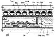
도 6은 멀티 챔버형의 제조 장치의 상면 모식도.
도 7은 표시 장치의 블록도를 설명하는 도면.
도 8은 신호선 구동 회로의 구성을 설명하는 도면.
도 9는 신호선 구동 회로의 동작을 설명하는 타이밍 차트.
도 10은 신호선 구동 회로의 동작을 설명하는 타이밍 차트.
도 11은 시프트 레지스터의 구성을 설명하는 도면.
도 12는 도 11에 도시하는 플립플롭의 접속 구성을 설명하는 도면.
도 13은 본 발명의 일 형태를 적용한 액정 표시 장치를 설명하는 도면.
도 14는 본 발명의 일 형태를 적용한 전자 페이퍼를 설명하는 도면.
도 15는 본 발명의 일 형태를 적용한 발광 표시 장치를 설명하는 도면.
도 16은 본 발명의 일 형태를 적용한 발광 표시 장치를 설명하는 도면.
도 17은 본 발명의 일 형태를 적용한 발광 표시 장치를 설명하는 도면.
도 18은 본 발명의 일 형태를 적용한 발광 표시 장치를 설명하는 도면.
도 19는 본 발명의 일 형태를 적용한 발광 표시 장치를 설명하는 도면.
도 20은 본 발명의 일 형태를 적용한 발광 표시 장치를 설명하는 도면.
도 21은 본 발명의 일 형태를 적용한 전자 기기를 설명하는 도면.
도 22는 본 발명의 일 형태를 적용한 전자 기기를 설명하는 도면.
도 23은 본 발명의 일 형태를 적용한 전자 기기를 설명하는 도면.
도 24는 본 발명의 일 형태를 적용한 전자 기기를 설명하는 도면.
도 25는 본 발명의 일 형태를 적용한 전자 기기를 설명하는 도면.BRIEF DESCRIPTION OF THE DRAWINGS Fig. 1 is a view for explaining a semiconductor device to which an embodiment of the present invention is applied; Fig.
2 is a view for explaining a method of manufacturing a semiconductor device to which an embodiment of the present invention is applied.
3 is a view for explaining a method of manufacturing a semiconductor device to which an embodiment of the present invention is applied.
4 is a view for explaining a manufacturing method of a semiconductor device to which an embodiment of the present invention is applied;
5 is a view for explaining a semiconductor device to which an embodiment of the present invention is applied.
6 is a schematic top view of a multi-chamber type manufacturing apparatus.
7 is a view for explaining a block diagram of a display device;
8 is a view for explaining a configuration of a signal line driver circuit;
9 is a timing chart for explaining the operation of the signal line driver circuit.
10 is a timing chart for explaining the operation of the signal line driver circuit.
11 is a view for explaining a configuration of a shift register;
12 is a view for explaining a connection configuration of the flip-flop shown in Fig.
13 is a view for explaining a liquid crystal display device to which an embodiment of the present invention is applied.
14 is a view for explaining an electronic paper to which an embodiment of the present invention is applied;
15 is a view for explaining a light emitting display device to which an embodiment of the present invention is applied.
16 is a view for explaining a light emitting display device to which an embodiment of the present invention is applied.
17 is a view for explaining a light emitting display device to which an embodiment of the present invention is applied.
18 is a view for explaining a light emitting display device to which an embodiment of the present invention is applied.
19 is a view for explaining a light emitting display device to which an embodiment of the present invention is applied.
20 is a view for explaining a light emitting display device to which an embodiment of the present invention is applied;
21 is a view for explaining an electronic apparatus to which an embodiment of the present invention is applied;
22 is a view for explaining an electronic apparatus to which an embodiment of the present invention is applied;
23 is a view for explaining an electronic apparatus to which an embodiment of the present invention is applied;
24 is a view for explaining an electronic apparatus to which an embodiment of the present invention is applied;
25 is a view for explaining an electronic apparatus to which an embodiment of the present invention is applied;
이하에서는 본 발명의 실시형태에 대하여 도면을 사용하여 상세하게 설명한다. 단, 본 발명은 이하의 설명에 한정되지 않고, 본 발명의 취지 및 그 범위로부터 벗어남이 없이 그 형태 및 상세를 다양하게 변경할 수 있다는 것은, 당업자라면 용이하게 이해된다. 따라서, 본 발명은 이하에 나타내는 실시형태의 기재 내용에 한정하여 해석되는 것은 아니다, 또한, 이하에 설명하는 본 발명의 구성에 있어서, 동일 부분 또는 동일한 기능을 갖는 부분에는 동일한 부호를 다른 도면 간에서 공통적으로 사용하고, 그 반복 설명은 생략한다.Hereinafter, embodiments of the present invention will be described in detail with reference to the drawings. However, it is to be understood by those skilled in the art that the present invention is not limited to the following description, and that various changes in form and detail can be made without departing from the spirit and scope of the present invention. Therefore, the present invention should not be construed as being limited to the description of the embodiments described below. Further, in the constitution of the present invention described below, And the repetitive description thereof will be omitted.
(실시형태 1)(Embodiment 1)
본 실시형태에서는 In, Ga, 및 Zn을 포함하는 산화물 반도체층을 사용하여, 반도체층과 소스 전극층 및 드레인 전극층의 사이에 버퍼층을 형성하고, 채널 보호층을 형성한 역스태거형(보텀 게이트 구조)의 박막 트랜지스터의 제작 공정에 대하여, 도 1 및 도 2를 사용하여 설명한다.(Bottom gate structure) in which a buffer layer is formed between a semiconductor layer and a source electrode layer and a drain electrode layer and a channel protective layer is formed using an oxide semiconductor layer containing In, Ga, and Zn, Will be described with reference to Figs. 1 and 2. Fig.
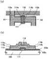
도 1에 본 실시형태의 보텀 게이트 구조의 박막 트랜지스터의 제작 공정을 도시한다. 도 2a는 도 1의 공정을 거쳐서 제작한 박막 트랜지스터의 평면도이고, 도 2b는 도 2a에 있어서의 A1-A2로 절단한 단면도이다.Fig. 1 shows a manufacturing process of a thin film transistor of the bottom gate structure of this embodiment. 2A is a plan view of a thin film transistor fabricated through the process of FIG. 1, and FIG. 2B is a cross-sectional view taken along line A1-A2 in FIG. 2A.
기판(100)은 바륨 보로 실리케이트 유리, 알루미노 보로 실리케이트 유리 또는 알루미노 실리케이트 유리 등, 퓨전(fusion)법이나 플로트(float)법으로 제작되는 무알칼리 유리 기판, 세라믹 기판 외, 본 제작 공정의 처리 온도에 견딜 수 있는 내열성을 갖는 플라스틱 기판 등을 사용할 수 있다. 또한, 스테인리스 합금 등의 금속 기판의 표면에 절연막을 형성한 기판을 적용하여도 좋다. 기판(100)이 마더 유리인 경우, 기판의 크기는 제 1 세대(320mm×400mm), 제 2 세대(400mm×500mm), 제 3 세대(550mm×650mm), 제 4 세대(680mm×880mm 또는 730mm×920mm), 제 5 세대(1000mm×1200mm 또는 1100m×1250mm), 제 6 세대(1500m×1800mm), 제 7 세대(1900mm×2200mm), 제 8 세대(2160mm×2460mm), 제 9 세대(2400mm×2800mm, 2450mm×3050mm), 제 10 세대(2950mm×3400mm) 등을 사용할 수 있다.The
또한 기판(100) 위에 하지막으로서 절연막을 형성하여도 좋다. 하지막으로서는 CVD법이나 스퍼터링법 등을 사용하여, 산화규소막, 질화규소막, 산화 질화규소막, 또는 질화산화규소막의 단층 또는 적층으로 형성하면 좋다.Further, an insulating film may be formed as a base film on the
게이트 전극층(111)은 금속 재료로 형성된다. 금속 재료로서는, 알루미늄, 크롬, 티타늄, 탄탈, 몰리브덴, 구리 등이 적용된다. 게이트 전극의 적합 예는 알루미늄 또는 알루미늄과 배리어 금속의 적층 구조체에 의해서 형성된다. 배리어 금속으로서는 티타늄, 몰리브덴, 크롬 등의 고융점 금속이 적용된다. 배리어 금속은 알루미늄의 힐록 방지, 산화 방지를 위해서 형성되는 것이 바람직하다.The
게이트 전극층(111)이 되는 반도체막은 두께 50nm 이상 300nm 이하로 형성된다. 게이트 전극의 두께를 300nm 이하로 함으로써, 후에 형성되는 반도체막이나 배선의 단절 방지가 가능하다. 또한, 게이트 전극의 두께는 150nm 이상으로 함으로써, 게이트 전극의 저항을 저감하는 것이 가능하며, 대면적화가 가능하다.The semiconductor film to be the
또한, 게이트 전극층(111) 위에 반도체막이나 배선을 형성하기 때문에, 단 절 방지를 위해 단부가 테이퍼 형상으로 되도록 가공하는 것이 바람직하다. 또한, 도시하지 않지만 이 공정에서 게이트 전극에 접속하는 배선이나 용량 배선도 동시에 형성할 수 있다.Further, since the semiconductor film or the wiring is formed on the
게이트 전극층(111)은 스퍼터링법, CVD법, 도금법, 인쇄법, 또는 은, 금, 구리 등의 도전성 나노 페이스트를 사용하여 잉크젯법에 의해 도전성 입자 등을 포함하는 액적을 토출하여 소성하여, 게이트 전극층(111)을 형성할 수 있다.The
또한, 여기서는 기판 위에 도전막으로서 알루미늄막과 몰리브덴막을 스퍼터링법에 의해 적층하여 성막하고, 본 실시형태에 있어서의 제 1 포토 마스크를 사용하여 형성한 레지스트 마스크를 사용하여, 기판 위에 형성된 도전막을 에칭하여 게이트 전극층(111)을 형성한다.Here, an aluminum film and a molybdenum film are deposited as a conductive film on the substrate by sputtering, and a conductive film formed on the substrate is etched by using a resist mask formed by using the first photomask in this embodiment A
게이트 절연막(102a, 102b)은 각각, 두께 50 내지 150nm의 산화규소막, 질화규소막, 산화질화규소막, 또는 질화산화규소막으로 형성할 수 있다. 또한 게이트 절연막을 2층으로 하지 않고, 산화규소막, 질화규소막, 산화질화규소막, 또는 질화산화규소막의 단층으로 형성할 수 있고, 또한, 3층의 게이트 절연막을 형성하여도 좋다.Each of the
게이트 절연막(102a)을 질화규소막, 또는 질화산화규소막을 사용하여 형성함으로써, 기판과 게이트 절연막(102a)의 밀착력을 높이고, 기판으로서 유리 기판을 사용한 경우, 기판으로부터의 불순물이 반도체층(113)으로 확산하는 것을 방지할 수 있고, 또한 게이트 전극층(111)의 산화 방지가 가능하다. 즉, 막 박리를 방지할 수 있는 것과 함께 후에 형성되는 박막 트랜지스터의 전기 특성을 향상시킬 수 있다. 또한, 게이트 절연막(102a, 102b)은 각각 두께 50nm 이상이면, 게이트 전극층(111)의 요철을 피복할 수 있기 때문에 바람직하다.When the
여기에서는 산화질화규소막이란, 그 조성으로서, 질소보다도 산소의 함유량이 많은 것이며, 농도 범위로서 산소가 55 내지 65at.%, 질소가 1 내지 20at.%, Si가 25 내지 35at.%, 수소가 0.1 내지 10at.%의 범위에서 포함되는 것을 말한다. 또한, 산화질화규소막은, 그 조성으로서, 산소보다도 질소의 함유량이 많은 것이며, 농도 범위로서 산소가 15 내지 30at.%, 질소가 20 내지 35at.%, Si가 25 내지 35at.%, 수소가 15 내지 25at.%의 범위로 포함되는 것을 말한다.Here, the silicon oxynitride film refers to a film having a larger oxygen content than nitrogen and having a concentration range of 55 to 65 atomic%, nitrogen of 1 to 20 atomic%, Si of 25 to 35 atomic%, hydrogen of 0.1 To 10 at.%. The silicon oxynitride film has a nitrogen content higher than that of oxygen and has a concentration range of 15-30 at.% Oxygen, 20-35 at.% Nitrogen, 25-35 at.% Si, 25at.%.
또한, 반도체층(113)에 접하는 게이트 절연막(102b)으로서는, 예를 들면, 산화규소, 산화알루미늄, 산화마그네슘, 질화알루미늄, 산화이트륨, 산화하프늄을 사용할 수 있다.As the
게이트 절연막(102a, 102b)은 각각, CVD법이나 스퍼터링법 등을 사용하여 형성할 수 있다. 여기서는 도 1a와 같이 게이트 절연막(102a)으로서 질화규소막을 플라즈마 CVD에 의해 성막하고, 게이트 절연막(102b)으로서 산화규소막을 스퍼터링법으로 성막한다.Each of the
특히, 반도체막에 접하는 게이트 절연막(102b)과 반도체막(103)은 연속적으로 성막하는 것이 바람직하다. 연속적으로 성막함으로써, 수증기 등의 대기성분이나 대기 중에 부유하는 불순물 원소나 먼지로 인한 오염이 없는 적층 계면을 형성할 수 있으므로, 박막 트랜지스터 특성의 편차를 저감할 수 있다.In particular, the
액티브 매트릭스형의 표시 장치에 있어서는, 회로를 구성하는 박막 트랜지스터의 전기 특성이 중요하고, 이 전기 특성이 표시 장치의 특성을 좌우한다. 특히 박막 트랜지스터의 전기 특성 중, 임계값 전압(Vth)이 중요하다. 전계 효과 이동도가 높아도 임계값 전압이 높거나, 혹은 임계값 전압이 마이너스이면, 회로로서 제어하는 것이 곤란하다. 임계값 전압값이 높고, 임계값 전압값의 절대값이 큰 박막 트랜지스터의 경우에는, 구동 전압이 낮은 상태에서는 박막 트랜지스터로서의 스위칭 기능을 다할 수 없으며, 부하가 될 우려가 있다. 또한, 임계값 전압값이 마이너스이면, 게이트 전압이 0V라도 소스 전극과 드레인 전극의 사이에 전류가 흐르는, 소위 노멀리 온(normally on)이 되기 쉽다.In the active matrix type display device, the electrical characteristics of the thin film transistors constituting the circuit are important, and the electrical characteristics thereof determine the characteristics of the display device. Particularly, among the electric characteristics of the thin film transistor, the threshold voltage (Vth) is important. If the threshold voltage is high or the threshold voltage is negative even though the field effect mobility is high, it is difficult to control it as a circuit. In the case of a thin film transistor in which the threshold voltage value is high and the absolute value of the threshold voltage value is large, the switching function as the thin film transistor can not be performed in a state where the driving voltage is low, and there is a fear of a load. Further, if the threshold voltage value is negative, even if the gate voltage is 0V, a so-called normally on state in which a current flows between the source electrode and the drain electrode is likely to occur.
n채널형의 박막 트랜지스터의 경우, 게이트 전압에 정(正)의 전압을 인가하여 비로소 채널이 형성되고, 드레인 전류가 흐르는 트랜지스터가 바람직하다. 구동 전압을 높게 하지 않으면 채널이 형성되지 않는 트랜지스터나, 부(負)의 전압 상태에서도 채널이 형성되어 드레인 전류가 흐르는 트랜지스터는 회로에 사용하는 박막 트랜지스터로서 부적합하다. 따라서, In, Ga, 및 Zn을 포함하는 산화물 반도체막을 사용하는 박막 트랜지스터의 게이트 전압이 0V에 가능한 한 가까운 정의 임계값 전압으로 채널이 형성되는 것이 바람직하다.In the case of an n-channel thin film transistor, it is preferable that a channel is formed by applying a positive voltage to the gate voltage, and a drain current flows. A transistor in which a channel is not formed unless the driving voltage is increased or a transistor in which a channel is formed even in a negative voltage state and a drain current flows is not suitable as a thin film transistor used in a circuit. Therefore, it is preferable that the channel is formed at a positive threshold voltage as close as possible to a gate voltage of 0 V of a thin film transistor using an oxide semiconductor film containing In, Ga, and Zn.
박막 트랜지스터의 임계값 전압은 산화물 반도체층의 계면, 즉, 산화물 반도체층과 게이트 절연막의 계면에 크게 영향을 준다고 생각된다. 그래서 이들의 계면을 청정한 상태로 형성함으로써, 박막 트랜지스터의 전기 특성을 향상시키는 동시에, 제조 공정의 복잡화를 방지할 수 있고, 양산성과 고성능의 양쪽을 갖춘 박막 트랜지스터를 실현한다.It is considered that the threshold voltage of the thin film transistor largely affects the interface of the oxide semiconductor layer, that is, the interface between the oxide semiconductor layer and the gate insulating film. Therefore, by forming these interfaces in a clean state, it is possible to improve the electrical characteristics of the thin film transistor, to prevent the complication of the manufacturing process, and to realize the thin film transistor having both the mass production and the high performance.
특히 산화물 반도체층과 게이트 절연막의 계면에 수분이 존재하면, 박막 트랜지스터의 전기적 특성의 열화, 임계값 전압의 편차, 노멀리 온으로 되기 쉬운 문제를 초래한다. 산화물 반도체층과 게이트 절연막을 연속적으로 성막함으로써, 이러한 수소 화합물을 배제할 수 있다.Particularly, when moisture is present at the interface between the oxide semiconductor layer and the gate insulating film, the electrical characteristics of the thin film transistor are deteriorated, the threshold voltage is deviated, and the problem of easily becoming a normally on is caused. By continuously forming the oxide semiconductor layer and the gate insulating film, such a hydrogen compound can be excluded.
따라서, 대기에 노출되지 않고 게이트 절연막과, 반도체막을 스퍼터링법에 의해 감압하에서 연속적으로 성막함으로써 양호한 계면을 갖고, 리크 전류가 낮고, 또한, 전류 구동 능력이 높은 박막 트랜지스터를 실현할 수 있다.Therefore, a thin film transistor having a good interface, a low leakage current, and a high current driving capability can be realized by continuously forming the gate insulating film and the semiconductor film under a reduced pressure by the sputtering method without exposure to the atmosphere.
또한, 본 명세서 중에서 연속 성막이란, 스퍼터링법으로 행하는 제 1 성막 공정으로부터 스퍼터링법으로 행하는 제 2 성막 공정까지의 일련의 프로세스 중, 피처리 기판이 놓여져 있는 분위기가 대기 등의 오염 분위기에 접촉하지 않고, 항상 진공 중 또는 불활성 가스 분위기(질소 분위기 또는 희가스 분위기)에서 제어되는 것을 말한다. 연속적으로 성막함으로써, 청정화된 피처리 기판으로의 수분 등의 재부착을 회피하고 성막을 행할 수 있다.In the present specification, the term "continuous film formation" means that, during a series of processes from the first film formation step performed by the sputtering method to the second film formation step performed by the sputtering method, the atmosphere in which the substrate is placed is not in contact with the contaminated atmosphere , It is always controlled in a vacuum or in an inert gas atmosphere (nitrogen atmosphere or rare gas atmosphere). By continuously forming the film, it is possible to prevent the re-adhesion of moisture and the like to the cleaned target substrate and to perform the film formation.
동일 챔버 내에서 제 1 성막 공정으로부터 제 2 성막 공정까지의 일련의 프로세스를 행하는 것은 명세서에 있어서의 연속 성막의 범위에 있는 것으로 한다.It is assumed that the series of processes from the first film forming step to the second film forming step in the same chamber is within the scope of continuous film formation in the specification.
또한, 상이한 챔버에서 제 1 성막 공정으로부터 제 2 성막 공정까지의 일련의 프로세스를 행하는 경우, 제 1 성막 공정을 끝낸 후, 대기에 노출하지 않고 챔버 간을 기판 반송하여 제 2 성막을 실시하는 것도 본 명세서에 있어서의 연속 성막의 범위에 있는 것으로 한다.When a series of processes from the first film forming step to the second film forming step are performed in different chambers, it is also possible to perform the second film forming by carrying the substrates between the chambers without exposing them to the atmosphere after the first film forming step is completed Is within the scope of continuous film formation in the specification.
또한, 제 1 성막 공정과 제 2 성막 공정의 사이에, 기판 반송 공정, 얼라인먼트 공정, 서냉(徐冷) 공정 또는 제 2 공정에 필요한 온도로 하기 위해서 기판을 가열 또는 냉각하는 공정 등을 갖더라도, 본 명세서에 있어서의 연속 성막의 범위에 있는 것으로 한다.Even if the substrate has a step of heating or cooling the substrate to a temperature required for the substrate transporting step, the aligning step, the slow cooling step or the second step between the first film forming step and the second film forming step, And is within the scope of continuous film formation in this specification.
단, 세정 공정, 웨트 에칭, 레지스트 형성과 같은 액체를 사용하는 공정이 제 1 성막 공정과 제 2 성막 공정의 사이에 있는 경우, 본 명세서에서 말하는 연속 성막의 범위에는 적합하지 않는 것으로 한다.However, when a process using a liquid such as a cleaning process, a wet etching process, or a resist process is performed between the first film forming process and the second film forming process, it is not suitable for the range of the continuous film forming described in this specification.
또한, 게이트 절연막, 반도체층 및 채널 보호층은 산소 분위기 하(또는 산소 90% 이상, 희가스(아르곤 등) 10% 이하)에서 형성함으로써, 열화에 의한 신뢰성의 저하나, 박막 트랜지스터 특성의 노멀리 온측으로의 시프트 등을 경감할 수 있다. 또한, n형의 도전형을 갖는 버퍼층은 희가스(아르곤 등) 분위기 하에서 성막하는 것이 바람직하다.Further, the gate insulating film, the semiconductor layer, and the channel protective layer are formed in an oxygen atmosphere (or at least 90% of oxygen and 10% or less of rare gas (argon, etc.)), And the like can be reduced. The buffer layer having the n-type conductivity is preferably formed in a rare gas (argon, etc.) atmosphere.
이렇게 스퍼터링법을 사용하여 연속적으로 성막하면, 생산성이 높고, 박막 계면의 신뢰성이 안정한다. 또한 게이트 절연막과 반도체층을 산소 분위기 하에서 성막하고, 산소를 많이 포함시키도록 하면, 열화에 의한 신뢰성의 저하나, 박막 트랜지스터가 노멀리 온으로 되는 것을 특징으로 하는 것을 경감할 수 있다.When the film is continuously formed by the sputtering method, the productivity is high and the reliability of the thin film interface is stable. Further, when the gate insulating film and the semiconductor layer are formed in an oxygen atmosphere to contain a large amount of oxygen, it is possible to reduce the reliability due to deterioration and the feature that the thin film transistor becomes normally on.
또한, 채널 보호층(116)이 되는 절연막(106)에 대해서도 반도체막(103)의 성막에 계속하여, 연속적으로 성막하는 것이 바람직하다. 연속적으로 성막함으로써, 반도체막(103)의 게이트 절연막과 접하는 면과는 반대측의 영역, 소위 백 채널에 수증기 등의 대기 성분이나 대기 중에 부유하는 불순물 원소나 먼지로 인한 오염이 없는 적층 계면을 형성할 수 있기 때문에, 박막 트랜지스터 특성의 편차를 저감할 수 있다.It is also preferable that the insulating
연속적으로 성막하는 방법으로서, 복수의 성막실을 가진 멀티 챔버형의 스퍼터링 장치나 복수의 타깃을 가진 스퍼터링 장치 또는 PLD(펄스 레이저 증착) 장치를 사용하면 좋다.As a continuous film formation method, a multi-chamber sputtering apparatus having a plurality of deposition chambers, a sputtering apparatus having a plurality of targets, or a PLD (Pulsed Laser Deposition) apparatus may be used.
절연막으로서 산화규소를 형성하는 경우, 타깃으로서 산화규소(인공 석영) 또는 규소를 사용하여, 고주파 스퍼터링법 또는 반응성 스퍼터링법에 의해 성막할 수 있다.When silicon oxide is formed as an insulating film, silicon oxide (artificial quartz) or silicon can be used as a target to form a film by a high-frequency sputtering method or a reactive sputtering method.
또한, 여기에서는 규소 타깃과 반도체막용의 타깃을 구비한 멀티 챔버형의 스퍼터링 장치를 사용하여, 반도체에 접하는 2층째의 게이트 절연막(102b)으로서 산화규소막을 형성하고, 대기에 노출시키지 않고 반도체막(103)의 형성과 채널 보호층이 되는 절연막(106)을 형성한다.Here, a silicon oxide film is formed as a second-layer
반도체막(113)은 비정질의 산화물 반도체막으로 형성된다. 비정질의 산화물 반도체막으로서는 인듐, 갈륨, 알루미늄, 아연 및 주석으로부터 선택한 원소의 복합 산화물을 사용할 수 있다.The
산화인듐과 산화갈륨과 산화아연으로 이루어지는 산화물의 경우, 금속 원소의 조성비의 자유도는 높고, 넓은 범위의 혼합비로 반도체층으로서 기능한다. 예를 들면 산화인듐과 산화갈륨과 산화아연을 각각 등몰로 혼합한 재료나, 막 중의 금속 원소의 존재비가 In:Ga:Zn=2.2:2.2:1.0의 비로 존재하는 산화물을 일 예로서 들 수 있다.In the case of an oxide composed of indium oxide, gallium oxide and zinc oxide, the degree of freedom of the composition ratio of the metal element is high and functions as a semiconductor layer in a wide mixing ratio. For example, a material in which indium oxide, gallium oxide, and zinc oxide are equally mixed, or an oxide in which the existence ratio of the metal element in the film is present in a ratio of In: Ga: Zn = 2.2: 2.2: 1.0 .
반도체막(103)으로서는 2nm 이상 200nm 이하, 바람직하게는 20nm 이상 150nm 이하의 두께로 형성하면 좋다. 또한, 막 중의 산소 결손이 증가하면 캐리어 농도가 높아지고, 박막 트랜지스터 특성이 손상받게 되므로, 예를 들면 산소만의 분위기 하, 또는 산소가 90% 이상, 또한, Ar이 10% 이하의 분위기 하에서 펄스 DC 스퍼터링법의 스퍼터링을 행하고, 산소 과잉의 IGZO막을 형성한다.The
비정질의 산화물 반도체는 반응성 스퍼터링법, 펄스 레이저법(PLD법) 또는 졸겔법에 의해 성막할 수 있다. 기상법 중에서도 재료계의 조성을 제어하기 쉬운 점에서는 PLD법이 적합하고, 양산성의 점에서는 상술한 바와 같이 스퍼터링법이 적합하다. 여기서는 반도체층의 형성 방법의 일예로서, In, Ga, 및 Zn을 포함하는 산화물(IGZO)을 사용한 방법에 대하여 설명한다.The amorphous oxide semiconductor can be formed by a reactive sputtering method, a pulsed laser method (PLD method), or a sol-gel method. Of the vapor-phase methods, the PLD method is suitable for controlling the composition of the material system easily, and the sputtering method is suitable for mass productivity. Here, as an example of a method of forming a semiconductor layer, a method using an oxide (IGZO) containing In, Ga, and Zn will be described.
산화인듐(In2O3)과 산화갈륨(Ga2O3)과 산화아연(ZnO)을 각각 등몰로 혼합하고, 소결(燒結)한 직경 8인치의 타깃을 사용하여, 타깃으로부터 170mm의 위치에 기판을 배치하고, 500W의 출력으로 DC(Direct Current) 스퍼터링하여 반도체층을 형성한다. 챔버의 압력은 0.4Pa, 가스 조성비는 Ar/O2가 10/5sccm의 조건에서 50nm 성막한다. 성막 시의 산소 분압을 인듐주석 산화물(ITO) 등의 투명 도전막의 성막 조건보다 높게 설정하고, 성막 분위기의 산소 농도를 제어하여 산소 결손을 억제하는 것이 바람직하다. 또한 펄스 전류(DC) 전원을 사용하면, 먼지를 경감할 수 있고, 반도체층의 막 두께 분포를 균일하게 할 수 있기 때문에 바람직하다.A target of 8 inches in diameter obtained by mixing and sintering indium oxide (In2 O3 ), gallium oxide (Ga2 O3 ) and zinc oxide (ZnO) A substrate is placed and DC (direct current) sputtering is performed at an output of 500 W to form a semiconductor layer. The pressure of the chamber is 0.4 Pa, and the gas composition ratio is 50 nm in a condition of Ar / O2 of 10/5 sccm. It is preferable to set the oxygen partial pressure at the time of film formation to be higher than the film forming condition of the transparent conductive film such as indium tin oxide (ITO), and to control the oxygen concentration in the film forming atmosphere to suppress oxygen deficiency. Use of a pulsed current (DC) power supply is preferable because dust can be reduced and the film thickness distribution of the semiconductor layer can be made uniform.
또한, 반도체막(103)에 플라즈마 처리를 행하여도 좋다. 플라즈마 처리를 행함으로써, 반도체막(103)의 대미지를 회복할 수 있다. 플라즈마 처리는 O2, N2O, 바람직하게는 산소를 포함하는 N2, He, Ar 분위기하에서 행하는 것이 바람직하다. 또한, 상기 분위기에 Cl2, CF4를 더한 분위기하에서 행하여도 좋다. 또한 플라즈마 처리는 무바이어스로 행하는 것이 바람직하다.Further, the
또, 본 실시형태에서는 산화물 반도체막용의 타깃과 함께 규소 타깃을 구비한 멀티 챔버형의 스퍼터링 장치를 사용하여, 이전 공정에서 형성한 게이트 절연막(102b)을 대기에 노출시키지 않고, 그 위에 반도체막(103)을 형성한다. 또한, 성막한 반도체막(103)을 대기에 노출시키지 않고, 그 위에 채널 보호층이 되는 절연막(106)을 성막한다.In this embodiment, a multi-chamber sputtering apparatus having a silicon target and a target for an oxide semiconductor film is used to form a
채널 보호층(116)은 반도체층의 채널 형성 영역과 중첩하는 영역에 절연막을 형성한다. 채널 보호층이 되는 절연막(106)은 무기재료(산화규소, 질화규소, 산화질화규소, 질화산화규소 등)를 사용할 수 있다. 또한, 감광성 또는 비감광성의 유기재료(유기 수지 재료)(폴리이미드, 아크릴, 폴리아미드, 폴리이미드아미드, 레지스트, 벤조시클로부텐 등), 또는 복수종으로 이루어지는 막, 또는 이들의 막의 적층 등을 사용할 수 있다. 또한, 실록산을 사용하여도 좋다.The channel
채널 보호층이 되는 절연막(106)은 플라즈마 CVD법이나 열 CVD법 등의 기상 성장법이나 스퍼터링법으로 성막할 수 있다. 또한, 습식법인 스핀코팅법 등의 도포법을 사용할 수 있다. 또한, 액적 토출법이나, 인쇄법(스크린 인쇄나 오프셋 인쇄 등 패턴이 형성되는 방법) 등에 의해서 선택적으로 형성하여도 좋다.The insulating
또한, 여기서는 규소 타깃과 산화물 반도체막용의 타깃을 구비한 멀티 챔버형의 스퍼터링 장치를 사용하여, 이전 공정에서 형성한 반도체막(103)을 대기에 노출하지 않고, 절연막(106)으로서 산화규소막을 성막한다.Here, a silicon oxide film is deposited as the insulating
다음으로, 본 실시형태에 있어서의 제 2 포토 마스크를 사용하여 레지스트 마스크(117)를 도 1a와 같이 형성한다. 레지스트 마스크(117)를 사용하여, 반도체막(103) 위에 형성된 절연막(106)을 선택적으로 에칭하여 도 1b에 도시하는 바와 같이 채널 보호층(116)을 형성한다.Next, a resist
다음으로, 반도체막(103) 위에 버퍼층으로서 기능하는 n형의 도전형을 갖는 막(104)을 성막한다. 버퍼층은 n+층으로서 기능하고, 드레인 영역 또는 소스 영역이라고도 부를 수 있다. 또한, 반도체층과 버퍼층의 사이에 캐리어 농도가 반도체층보다 높고, 버퍼층보다 낮은 제 2 버퍼층을 형성하여도 좋다. 제 2 버퍼층은 n-층으로서 기능한다.Next, a
버퍼층으로서는 n형의 도전형을 갖는 금속 산화물이나 In, Ga, 및 Zn을 포함하는 산화물 반도체막을 사용할 수 있다.As the buffer layer, a metal oxide having an n-type conductivity or an oxide semiconductor film containing In, Ga, and Zn can be used.
버퍼층에 사용할 수 있는 n형의 도전형을 갖는 금속 산화물로서는 예를 들면 산화티타늄, 산화몰리브덴, 산화아연, 산화인듐, 산화텅스텐, 산화마그네슘, 산화칼슘, 산화주석 등을 사용할 수 있다. 버퍼층에는 n형 또는 p형의 도전형을 부여하는 불순물을 포함시켜도 좋다. 불순물로서는, 인듐, 갈륨, 알루미늄, 아연, 주석 등을 사용할 수 있다. 특히, 버퍼층이 티타늄을 포함하는 것이 바람직하다. 금속 산화물로 이루어지는 버퍼층의 캐리어 농도는 채널이 형성되는 IGZO 반도체층(113)보다도 높고 도전성이 우수하기 때문에, 소스 전극층 또는 드레인 전극층과 반도체층이 직접 접합하는 경우와 비교하여, 접촉 저항을 저감할 수 있다.As the metal oxide having an n-type conductivity which can be used for the buffer layer, for example, titanium oxide, molybdenum oxide, zinc oxide, indium oxide, tungsten oxide, magnesium oxide, calcium oxide and tin oxide can be used. The buffer layer may contain an impurity imparting n-type or p-type conductivity. As the impurities, indium, gallium, aluminum, zinc, tin and the like can be used. In particular, it is preferable that the buffer layer contains titanium. Since the carrier concentration of the buffer layer made of the metal oxide is higher than that of the
또한, 버퍼층으로서 n형의 도전형을 갖는 In, Ga, 및 Zn을 포함하는 산화물 반도체막을 사용할 수도 있다. 또한 In, Ga, 및 Zn을 포함하는 산화물 반도체막에 n형을 부여하는 불순물 원소를 포함시켜도 좋다. 불순물 원소로서, 예를 들면, 마그네슘, 알루미늄, 티타늄, 스칸듐, 이트륨, 지르코늄, 하프늄, 붕소, 탈륨, 게르마늄, 주석, 납 등을 사용할 수 있다. 마그네슘, 알루미늄, 티타늄 등을 버퍼층에 포함시키면, 산소의 블로킹 효과 등이 있고, 성막 후의 가열 처리 등에 의해서 반도체층의 산소 농도를 최적의 범위 내로 유지할 수 있다.As the buffer layer, an oxide semiconductor film containing In, Ga, and Zn having an n-type conductivity type may also be used. Further, the oxide semiconductor film containing In, Ga, and Zn may contain an impurity element imparting n-type conductivity. As the impurity element, for example, magnesium, aluminum, titanium, scandium, yttrium, zirconium, hafnium, boron, thallium, germanium, tin, lead and the like can be used. When magnesium, aluminum, titanium, or the like is included in the buffer layer, oxygen blocking effect and the like can be obtained, and the oxygen concentration of the semiconductor layer can be maintained within an optimum range by heat treatment after film formation.
또한, 반도체층과 버퍼층의 사이에, 반도체층보다 캐리어 농도가 높고 버퍼층보다 캐리어 농도가 낮은 n-층으로서 기능하는 제 2 버퍼층을 형성하여도 좋다.A second buffer layer functioning as an n- layer having a higher carrier concentration than the semiconductor layer and a lower carrier concentration than the buffer layer may be formed between the semiconductor layer and the buffer layer.
n형의 도전형을 갖는 막(104)으로서는 2nm 이상 100nm 이하의 두께로 형성하면 좋다.The
n형의 도전형을 갖는 막(104)은 스퍼터링법 또는 펄스 레이저 증착법(PLD법)에 의해 성막할 수 있다.The
다음으로, 소스 전극층 또는 드레인 전극층으로 이루어지는 도전막(105)을 성막한다. 도전막(105)은 게이트 전극층(111)과 동일한 재료를 사용할 수 있지만, 특히 n형의 도전형을 갖는 막(104)에 접하는 층이 티타늄막인 것이 적합하다. 도전막의 구체예로서, 단체(單體)의 티타늄막, 또는 티타늄막과 알루미늄막의 적층막, 또는 티타늄막과 알루미늄막과 티타늄막을 차례로 적층한 3층 구조로 하여도 좋다.Next, a
다음으로, 본 실시형태에 있어서의 제 3 포토 마스크를 사용하여 레지스트 마스크(118)를 도 1c와 같이 형성하고, 레지스트 마스크(118)를 사용하여, 채널 보호층(116) 위에 형성한 도전막(105)을 도 1d와 같이 에칭하여 분리하고, 소스 전극층 및 드레인 전극층(115a, 115b)을 형성한다.Next, a resist
또한, 동일한 레지스트 마스크(118)를 사용하여, n형의 도전형을 갖는 막(104)을 에칭하여 분리하고, 버퍼층(114a, 114b)을 형성한다.Further, by using the same resist
또한, 채널 보호층(116)은 에칭 공정 중에 채널 형성 영역에 대미지가 가해지는 것을 방지할 뿐만 아니라, 에칭 스토퍼로서도 기능한다. 즉 반도체막(103)의 불필요한 부분을 에칭하여 제거할 때, 채널 보호층(116)이 반도체층(113)의 채널 형성 영역의 소실을 막고 있다. 또한, 게이트 절연막(102b), 또는 게이트 절연막(102a)도 에칭 스토퍼로서도 기능하기 때문에, 반도체막(103)의 불필요한 부분의 에칭을 용이하게 한다. 그 결과, 소스 전극층 및 드레인 전극층(115a, 115b), 버퍼층(114a, 114b), 반도체층(113)을 상기 레지스트 마스크(118)로 형성할 수 있다.In addition, the channel
또한, 각각의 막은 드라이 에칭이나 웨트 에칭을 사용하여 가공하여도 좋고, 2회의 에칭으로 나누어 각각 선택적으로 에칭하여도 좋다.Each of the films may be processed by dry etching or wet etching, or may be selectively etched by dividing the film by two times of etching.
본 실시형태에 기재한 In, Ga, 및 Zn을 포함하는 산화물(IGZO)을 반도체층(113)에 사용한 박막 트랜지스터는, 형성한 반도체층(113)을 가열 처리함으로써, 특성이 개선된다. 구체적으로, 온 전류가 커지고, 트랜지스터 특성의 편차가 감소한다.In the thin film transistor using the oxide (IGZO) containing In, Ga, and Zn as the
반도체층(113)의 가열 처리 온도는 바람직하게는 300℃ 내지 400℃의 범위이고, 여기서는 350℃에서 1시간 가열 처리한다. 가열 처리는 반도체층(113)의 형성 후라면 행하여도 좋다. 예를 들면 게이트 절연막(102b)과 반도체막(103)과 채널 보호층이 되는 절연막(106)을 연속적으로 성막을 끝낸 후라도 좋고, 채널 보호층(116)을 패터닝하여 형성한 후라도 좋고, 버퍼층으로서 기능하는 n형의 도전형을 가지는 막(104)을 성막한 후라도 좋고, 도전막(105)을 형성한 후라도 좋다. 또한, 소스 전극층 및 드레인 전극층(115a, 115b)과 버퍼층(114a, 114b)과 반도체층(113)을 다 형성한 후라도 좋고, 박막 트랜지스터의 밀봉막을 형성한 후라도 좋고, 평탄화막의 형성 후에 행하는 열 경화 처리를 반도체층의 가열 처리와 겸해도 좋다.The heat treatment temperature of the
상술한 설명에 따라서, 도 2에 도시한 역스태거형(보텀 게이트 구조) 박막 트랜지스터를 제작한다.According to the above description, the reverse stagger type (bottom gate structure) thin film transistor shown in Fig. 2 is fabricated.
본 실시형태에서 제작한 박막 트랜지스터의 버퍼층(114a, 114b)의 캐리어 농도는 반도체층(113)보다도 높고 도전성이 우수하기 때문에, 소스 전극층 또는 드레인 전극층과 반도체층(113)이 직접 접합하는 경우와 비교하여, 접촉 저항을 저감할 수 있다. 또한, 소스 전극층 또는 드레인 전극층과 반도체층(113)의 접합 계면에 버퍼층(114a, 114b)을 끼워넣음으로써, 접합 계면에 집중하는 전계를 완화할 수 있다.Since the carrier concentration of the
또한, 채널 보호층(116)을 형성하는 구조이기 때문에, 산화물 반도체막의 게이트 절연막(102b)과 접하는 면과는 반대측의 영역, 소위 백 채널을 공정 시의 대미지(에칭 시의 플라즈마나 에칭제에 의한 막 감소나, 산화 등)로부터 보호할 수 있다. 따라서 박막 트랜지스터의 신뢰성을 향상시킬 수 있다.In addition, since the channel
또한 반도체층(113)에 접하는 게이트 절연막(102b)과 반도체층(113)과 채널 보호층을 연속적으로 성막하고 있기 때문에, 수증기 등의 대기 성분이나 대기 중에 부유하는 불순물 원소나 먼지로 인한 오염이 없는 적층 계면을 형성할 수 있기 때문에, 박막 트랜지스터 특성의 편차를 저감할 수 있다.In addition, since the
또한, 채널 보호층과 게이트 절연막을 에칭 스토퍼로서 이용함으로써, 제 3 포토 마스크를 사용하여 제작한 레지스트 마스크(118)에 의해, 소스 전극층 또는 드레인 전극층이 되는 도전막(105)과, 버퍼층이 되는 n형의 도전형을 갖는 막(104)과, 반도체막(103)을 에칭할 수 있어, 공정이 간편하게 된다.Further, by using the channel protective layer and the gate insulating film as the etching stopper, the
따라서, 본 발명의 일 형태를 적용함으로써, 광 전류가 적고, 기생 용량이 작고, 온·오프 비가 높은 박막 트랜지스터를 얻을 수 있고, 양호한 동작 특성(f 특성)을 갖는 박막 트랜지스터를 수율 좋게 제작할 수 있다. 전기 특성이 높고 신뢰성이 좋은 박막 트랜지스터를 갖는 반도체 장치를 생산성이 우수한 방법으로 제공할 수 있다.Therefore, by applying an embodiment of the present invention, a thin film transistor having a small photocurrent, a small parasitic capacitance and a high on / off ratio can be obtained, and a thin film transistor having good operation characteristics (f characteristics) can be manufactured with high yield . A semiconductor device having a thin film transistor having high electric characteristics and good reliability can be provided as a method with excellent productivity.
(실시형태 2)(Embodiment 2)
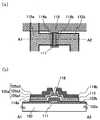
본 실시형태에서는 상기 실시형태 1과는 다른 구조의 버퍼층을 갖는 IGZO 반도체층을 사용한 역스태거형(보텀 게이트 구조) 박막 트랜지스터의 제작 공정에 대하여, 도 3 및 도 4를 사용하여 설명한다. 또한 본 실시형태에 있어서, 실시형태 1과 동일한 것에 대해서는 동일 부호를 사용하고, 상세한 설명을 생략한다.In this embodiment mode, a manufacturing process of a reverse stagger type (bottom gate structure) thin film transistor using an IGZO semiconductor layer having a buffer layer structure different from that of the first embodiment will be described with reference to FIGS. 3 and 4. FIG. In the present embodiment, the same symbols are used for the same elements as those in
도 3에 본 실시형태의 보텀 게이트 구조의 박막 트랜지스터의 제작 공정을 도시한다. 도 4a는 도 3의 공정을 거쳐서 제작한 박막 트랜지스터의 평면도이고, 도 4b는 도 4a에 있어서의 A1-A2로 절단한 단면도이다.Fig. 3 shows a manufacturing process of the thin film transistor of the bottom gate structure of this embodiment. FIG. 4A is a plan view of the thin film transistor fabricated through the process of FIG. 3, and FIG. 4B is a cross-sectional view taken along line A1-A2 in FIG. 4A.
본 실시형태에서는 투광성이 있는 기판(100)을 사용한다. 투광성이 있는 기판으로서는 예를 들면 바륨 보로 실리케이트 유리, 알루미노 보로 실리케이트 유리, 또는 알루미노 실리케이트 유리 등, 퓨전법이나 플로트법으로 제작되는 무알칼리 유리 기판 외에, 본 제작 공정의 처리 온도에 견딜 수 있는 내열성을 갖는 플라스틱 기판 등을 그 예로 들 수 있다. 또한, 본 실시형태 1과, 마찬가지로 기판(100) 위에 하지막으로서 절연막을 형성하여도 좋다.In the present embodiment, the
게이트 전극층(111)은 차광성을 갖는 금속 재료로 형성한다. 금속 재료로서는 알루미늄, 크롬, 티타늄, 탄탈, 몰리브덴, 구리 등이 적용된다. 게이트 전극의 적합한 예는 알루미늄 또는 알루미늄과 배리어 금속의 적층 구조체에 의해서 형성된다. 배리어 금속으로서는 티타늄, 몰리브덴, 크롬 등의 고융점 금속이 적용된다. 배리어 금속은 알루미늄의 힐록 방지, 산화 방지를 위해 형성하여도 바람직하다. 차광성을 갖는 게이트 전극층(111)의 두께 및 단부의 형상, 성막 방법 등은 실시형태 1과 마찬가지로 형성한다.The
또한, 여기에서는 기판 위에 도전막으로서 알루미늄막과 몰리브덴막을 스퍼터링법에 의해 성막하여 적층하고, 본 실시형태에 있어서의 제 1 포토 마스크를 사용하여 형성한 레지스트 마스크를 사용하여, 기판 위에 형성된 도전막을 에칭하여 게이트 전극층(111)을 형성한다.In this case, an aluminum film and a molybdenum film are deposited as a conductive film on the substrate by sputtering and laminated. Using the resist mask formed by using the first photomask in this embodiment mode, the conductive film formed on the substrate is etched And a
게이트 전극층(111) 위에 게이트 절연막(102a)과, 반도체막(103)에 접하는 게이트 절연막(102b)과 반도체막(103)과 채널 보호층이 되는 절연막(106)을 이 순서로 적층한다. 본 실시형태에 있어서는 게이트 절연막(102a, 102b)과 절연막(106)은 투광성의 절연 재료를 선택한다. 투광성이 있는 절연막으로서는, 산화규소막, 질화규소막, 산화질화규소막, 또는 질화산화규소막으로 형성할 수 있다. 또한, 투광성을 가지는 절연막의 두께, 성막 방법 등은 실시형태 1과 마찬가지로 형성한다.A
여기서는 게이트 절연막(102a)으로서 질화규소막을 플라즈마 CVD법으로 성막하고, 게이트 절연막(102b)으로서 산화규소막을 스퍼터링법으로 성막한다. 게이트 절연막(102b)과 반도체막(103)과 채널 보호층이 되는 절연막(106)은 실시형태 1과 마찬가지로, 연속 성막하여 적층한다. 연속 성막에 의해, 채널 영역 및 백 채널에 수증기 등의 대기 성분이나 대기 중에 부유하는 불순물 원소나 먼지로 인한 오염이 없는 적층 계면을 형성할 수 있다. 그 결과, 박막 트랜지스터의 특성의 편차를 저감하고, 오프 전류를 억제할 수 있다. 또한, In, Ga, 및 Zn을 포함하는 산화물(IGZ0)은 밴드갭(band gap)이 넓은 재료이기 때문에, IGZ0를 사용한 반도체막(103)은 광을 잘 투과한다.Here, a silicon nitride film is formed as a
다음으로, 절연막(106) 위에 포지티브형 포토레지스트막을 스핀코팅하여 형성한다. 여기에서의 공정에서 형성한 구조에 있어서, 게이트 전극층(111)만 차광성이므로, 기판(100)측으로부터 포토레지스트막을 노광하면, 포토레지스트의 게이트 전극층(111)과 중첩하는 영역만이 노광되지 않는다. 즉, 게이트 절연막이 포토 마스크로서 작용하고, 게이트 전극과 중첩하는 영역에 레지스트 마스크(117)를 형성할 수 있다(도 3a 참조).Next, a positive photoresist film is formed on the insulating
다음으로, 레지스트 마스크(117)를 사용하여, 절연막(106)을 에칭하여 채널 보호층(116)을 형성한다. 또한, 채널 보호층(116)의 에칭에 있어서, 반도체막(103)의 표면을 도 3b와 같이 약간 에칭하여도 좋다. 반도체막(103)의 표면을 에칭함으로써, 다음으로 적층하는 n형의 도전형을 갖는 막(104)과 양호한 접촉 상태로 할 수 있다.Next, using the resist
다음으로, 반도체막(103) 및 채널 보호층(116) 위에 버퍼층이 되는 n형의 도전형을 갖는 막(104) 및 소스 전극층 및 드레인 전극층이 되는 도전막(105)을 실시형태 1과 동일한 방법으로 적층한다.Next, a
여기서는 도전막(105)으로서, 3층 적층막을 스퍼터링법에 의해 성막한다. 예를 들면 티타늄막(105-1)과 알루미늄막(105-2)과 티타늄막(105-3)으로 이루어지는 3층 적층막을 사용할 수 있다.Here, as the
다음으로, 본 실시형태에 있어서의 제 2 포토 마스크를 사용하여 형성한 레지스트 마스크(118)를 사용하여, 3층 적층막으로 이루어지는 도전막(105)을 에칭하고, 소스 전극층 또는 드레인 전극층이 되는 115a와 115b를 형성한다.Next, by using the resist
실시형태 1과 마찬가지로, 레지스트 마스크(118)를 사용하여 n형의 도전형을 갖는 막(104)을 에칭하여 버퍼층(114a, 114b)을 형성한다.The
또한, 레지스트 마스크(118)와 채널 보호층(116)을 마스크로 하여 반도체층(113)의 불필요한 부분을 에칭하여 제거한다. 도 3d는 n형의 도전형을 갖는 막(104)과 반도체막(103)의 에칭에 수반하여, 채널 보호층(116)의 표면이 약간 에칭되어 오목형으로 되어 있는 상태를 도시하지만, 채널 형성부로의 대미지를 막고 있으면 좋다. 또한, 박막 트랜지스터의 외형부의 게이트 절연막(102b)도 막 감소 또는 소실하고 있는 모양을 나타내지만, 박막 트랜지스터 내부의 게이트 절연막이 남아 있으면 좋다.Further, an unnecessary portion of the
형성한 반도체층(113)의 가열 처리는 실시형태 1과 마찬가지로 행한다.The heat treatment of the formed
본 발명에서는 게이트 전극층(111)을 포토 마스크로 하여 레지스트 마스크(117)를 형성하기 때문에, 포토 마스크의 사용 매수를 절감할 수 있을 뿐만 아니라, 얼라인먼트 어긋남이 발생하지 않는다. 또한, 채널 보호층(116)에 의해 반도체층(113)의 채널 형성 영역을 보호한 상태이기 때문에, 제 2 포토 마스크를 사용하여 제작한 레지스트 마스크(118)에 의해, 소스 전극층 또는 드레인 전극층이 되는 도전막(105)과, 버퍼층이 되는 n형의 도전형을 갖는 막(104)과, 반도체막(103)을 에칭할 수 있고, 공정이 간편하게 된다.In the present invention, since the resist
따라서, 본 발명의 일 형태를 적용함으로써, 광 전류가 적고, 기생 용량이 작고, 온·오프 비가 높은 박막 트랜지스터를 얻을 수 있고, 양호한 동(動) 특성(f 특성)을 갖는 박막 트랜지스터를 수율 좋게 제작할 수 있다. 또한, 전기 특성이 높고 신뢰성이 좋은 박막 트랜지스터를 갖는 반도체 장치를 생산성이 우수한 방법으로 제공할 수 있다.Therefore, by applying one embodiment of the present invention, it is possible to obtain a thin film transistor having a small photocurrent, a small parasitic capacitance and a high on / off ratio, and a thin film transistor having good dynamic characteristics (f characteristics) Can be produced. In addition, a semiconductor device having a thin film transistor having high electric characteristics and high reliability can be provided by a method with excellent productivity.
(실시형태 3)(Embodiment 3)
본 실시형태에서는 복수의 채널 형성 영역을 접속한 구조를 갖는 IGZO 반도체층을 사용한 박막 트랜지스터의 제작 방법에 대하여 도 5를 사용하여 설명한다.In the present embodiment, a method of manufacturing a thin film transistor using an IGZO semiconductor layer having a structure in which a plurality of channel forming regions are connected will be described with reference to FIG.
도 5a는 도전막(105) 위에 본 실시형태에 있어서의 제 3 포토 마스크를 사용하여 레지스트 마스크를 형성한 상태를 도시하는 단면도이다. 도 5b는 도전막(105), n형의 도전형을 갖는 막(104), 반도체막(103)을 에칭한 상태를 도시하는 단면도이다. 도 5c는 완성한 TFT의 평면도이고, 도 5d는 도 5c에 있어서의 A1-A2로 절단한 단면도이다. 또, 본 실시형태에 있어서, 실시형태 1과 동일한 것에 대해서는 동일한 부호를 사용하여 상세한 설명은 생략한다.5A is a cross-sectional view showing a state in which a resist mask is formed on the
본 실시형태에 있어서의 제 1 포토 마스크를 사용하여 형성한 레지스트 마스크를 사용하여, 실시형태 1과 마찬가지로 기판(100) 위에 게이트 전극층(111a, 111b)을 형성한다. 다음으로, 게이트 전극층(111a, 111b) 위에 게이트 절연막(102a)을 형성한다. 다음으로, 반도체막(103)에 접하는 게이트 절연막(102b)과 반도체막(103)과 채널 보호층이 되는 절연막(106)을 스퍼터링법에 의해 연속적으로 성막한다.The
본 실시형태에 있어서의 제 2 포토 마스크를 사용하여 형성한 레지스트 마스크를 사용하여 반도체층의 채널 형성 영역과 중첩하는 채널 보호층(116a, 116b)을 형성한다.The channel
다음으로, 반도체막(103) 및 채널 보호층(116) 위에, 버퍼층이 되는 n형 도전형을 갖는 막(104) 및 소스 전극층 또는 드레인 전극층이 되는 도전막(105)을 실시형태 1과 동일한 방법으로 적층한다.Next, a
본 실시형태에 있어서의 제 3 포토 마스크를 사용하여 도 5a와 같은 레지스트 마스크를 형성한 후, 도전막(105), n형의 도전형을 갖는 막(104), 반도체막(103)을 에칭한다. 도전막(105)은 소스 전극층 및 드레인 전극층(115a, 115b), 및 2개의 채널 형성 영역을 접속하는 도전층(115c)을 형성하고, n형의 도전형을 갖는 막(104)은 버퍼층(114a, 114b), 및 2개의 채널 형성 영역을 접속하는 n형의 도전형을 갖는 층(114c)을 형성하고, 반도체막(103)을 에칭하여 반도체층(113)을 형성한다(도 5b 참조). 또한 도 5d에는 소스 전극층 및 드레인 전극층(115a, 115b)의 단부가, 버퍼층(114a, 114b)으로부터 후퇴한 상태를 도시한다. 후퇴함으로써, 소스 전극과 드레인 전극의 사이에서 단락이 발생하기 어려워진다.After the resist mask as shown in Fig. 5A is formed by using the third photomask in this embodiment mode, the
또한, 본 실시형태에서는 2개의 채널 형성 영역을 접속한 구조를 제시하였지만, 이것에 한정되지 않고, 3개의 채널 형성 영역이 접속된 트리플 게이트 구조 등 소위 멀티 게이트 구조(직렬로 접속된 2개 이상의 채널 형성 영역을 갖는 구조)이어도 좋다.In the present embodiment, a structure in which two channel forming regions are connected is shown. However, the present invention is not limited to this, and a so-called multi-gate structure such as a triple gate structure in which three channel forming regions are connected Forming region).
또한, 본 실시형태에서 설명한 박막 트랜지스터의 2개의 채널 형성 영역은 반도체층(113)과 n형의 도전형을 갖는 층(114c)과 도전층(105c)으로 전기적으로 접속되어 있다.In addition, the two channel forming regions of the thin film transistor described in this embodiment are electrically connected to the
또한, 형성한 반도체층(113)의 가열 처리는 실시형태 1과 동일하게 행한다.The heat treatment of the formed
본 발명에서는 채널 보호층(116)에 의해 반도체층(113)의 채널 형성 영역을 보호한 상태이다. 또한, 제 3 포토 마스크를 사용하여 제작한 레지스트 마스크(118)에 의해, 소스 전극층 또는 드레인 전극층이 되는 도전막(105)과, 버퍼층이 되는 n형의 도전형을 갖는 막(104)과, 반도체막(103)을 에칭할 수 있고, 공정이 간편해진다. 또한, 이러한, 멀티 게이트 구조는 오프 전류값을 저감하는 데에 극히 유효하다.In the present invention, the channel forming region of the
따라서, 본 발명의 일 형태를 적용함으로써, 광 전류가 적고, 기생 용량이 작고, 온·오프 비가 높은 박막 트랜지스터를 얻을 수 있고, 양호한 동 특성(f 특성)을 갖는 박막 트랜지스터를 수율 좋게 제작할 수 있다. 또한, 전기 특성이 높고 신뢰성이 좋은 박막 트랜지스터를 갖는 반도체 장치를 생산성이 우수한 방법으로 제공할 수 있다.Therefore, by applying one embodiment of the present invention, it is possible to obtain a thin film transistor having a small photocurrent, a small parasitic capacitance, a high on / off ratio, and a thin film transistor having good copper characteristics (f characteristics) . In addition, a semiconductor device having a thin film transistor having high electric characteristics and high reliability can be provided by a method with excellent productivity.
(실시형태 4)(Fourth Embodiment)
여기서는 적어도 게이트 절연막과 산화물 반도체층의 적층을 대기에 노출하지 않고, 연속적으로 성막하는 역스태거형의 박막 트랜지스터의 제작예를 이하에 나타낸다. 여기서는 연속적으로 성막을 하는 공정까지의 공정을 나타내고, 그 후의 공정은 실시형태 1 내지 실시형태 3의 어느 하나에 따라서 박막 트랜지스터를 제작하면 좋다.Hereinafter, an example of fabricating a reverse stagger type thin film transistor in which at least a lamination of a gate insulating film and an oxide semiconductor layer is formed without exposing to the atmosphere is described below. Here, the process up to a step of forming a film continuously is shown, and a thin film transistor may be fabricated in accordance with any one of the first to third embodiments in subsequent steps.
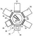
대기에 노출되지 않고 연속 성막을 행하는 경우, 도 6에 도시하는 바와 같은 멀티 챔버형의 제조 장치를 사용하는 것이 바람직하다.When continuous film formation is performed without being exposed to the atmosphere, it is preferable to use a multi-chamber type production apparatus as shown in Fig.
제조 장치의 중앙부에는 기판을 반송하는 반송 기구(대표적으로는 반송 로봇(81))를 구비한 반송실(80)이 설치되고, 반송실(80)에는 반송실 내로 반입 및 반출하는 기판을 복수매 수납하는 카세트 케이스를 세트하는 카세트실(82)이 연결되어 있다.A
또한, 반송실에는 각각 게이트 밸브(83 내지 88)를 통하여 복수의 처리실이 연결된다. 여기에서는 상면 형상이 육각형인 반송실(80)에 5개의 처리실을 연결하는 예를 나타낸다. 또, 반송실의 상면 형상을 변경함으로써, 연결할 수 있는 처리실의 수를 바꿀 수 있고, 예를 들면, 사각형으로 하면 3개의 처리실을 연결할 수 있고, 팔각형으로 하면 7개의 처리실을 연결할 수 있다.A plurality of processing chambers are connected to the transfer chamber through
5개의 처리실 중, 적어도 1개의 처리실은 스퍼터링을 행하는 스퍼터링 챔버로 한다. 스퍼터링 챔버는 적어도 챔버 내부에, 스퍼터 타깃, 타깃을 스퍼터하기 위한 전력 인가 기구나 가스 도입 수단, 소정 위치에 기판을 보유하는 기판 홀더 등이 설치되어 있다. 또한, 스퍼터링 챔버 내를 감압 상태로 하기 위해서, 챔버 내의 압력을 제어하는 압력 제어 수단이 스퍼터링 챔버에 설치되어 있다.Of the five treatment chambers, at least one treatment chamber is a sputtering chamber for performing sputtering. The sputtering chamber is provided with at least a sputtering target, a power applying mechanism and a gas introducing means for sputtering the target, and a substrate holder holding a substrate at a predetermined position, at least in the chamber. Further, in order to reduce the pressure inside the sputtering chamber, a pressure control means for controlling the pressure in the chamber is provided in the sputtering chamber.
스퍼터링법에는 스퍼터용 전원에 고주파 전원을 사용하는 RF 스퍼터링법, DC 스퍼터링법이 있고, 또한 펄스적으로 바이어스를 주는 펄스 DC 스퍼터링법도 있다. RF 스퍼터링법은 주로 절연막을 성막하는 경우에 사용되고, DC 스퍼터링법은 주로 금속막을 성막하는 경우에 사용된다.The sputtering method includes an RF sputtering method and a DC sputtering method in which a high frequency power source is used as a sputtering power source, and a pulse DC sputtering method in which a bias is applied in a pulsed manner. The RF sputtering method is mainly used for forming an insulating film, and the DC sputtering method is mainly used for forming a metal film.
또한, 재료가 다른 타깃을 복수 설치할 수 있는 다원 스퍼터링 장치도 있다. 다원 스퍼터링 장치는 동일 챔버에서 다른 재료막을 적층 성막하는 것도, 동일 챔버에서 복수 종류의 재료를 동시에 방전시켜서 성막할 수도 있다.There is also a multi-sputtering apparatus in which a plurality of targets with different materials can be installed. The multi-sputtering apparatus may be formed by laminating different material films in the same chamber or simultaneously discharging a plurality of kinds of materials in the same chamber.
또한, 챔버 내부에 자석 기구를 구비한 마그네트론 스퍼터링법을 사용하는 스퍼터링 장치나, 글로우 방전을 사용하지 않고 마이크로파를 사용하여 발생시킨 플라즈마를 사용하는 ECR 스퍼터링법을 사용하는 스퍼터링 장치가 있다.There is also a sputtering apparatus using a magnetron sputtering method having a magnet mechanism in a chamber or a sputtering apparatus using an ECR sputtering method using a plasma generated by using microwaves without using a glow discharge.
스퍼터링 챔버로서는 상술한 바와 같은 스퍼터링법을 적절하게 사용한다.As the sputtering chamber, the above-described sputtering method is suitably used.
또한 성막 방법으로서, 성막 중에 타깃 물질과 스퍼터 가스 성분을 화학 반응시켜서 이들의 화합물 박막을 형성하는 리액티브 스퍼터링법이나, 성막 중에 기판에도 전압을 가하는 바이어스 스퍼터링법도 있다.As a film forming method, there is also a reactive sputtering method in which a target material and a sputter gas component are chemically reacted to form a compound thin film during film formation, or a bias sputtering method in which a voltage is applied to a substrate during film formation.
또한 5개의 처리실 중, 다른 처리실의 하나는 스퍼터링 전에 기판의 예비 가열 등을 행하는 가열 챔버, 스퍼터링 후에 기판을 냉각하는 냉각 챔버, 또는 플라즈마 처리를 행하는 챔버로 한다.Of the five treatment chambers, one of the other treatment chambers is a heating chamber for preheating the substrate before sputtering, a cooling chamber for cooling the substrate after sputtering, or a chamber for plasma treatment.
다음으로 제조 장치의 동작의 일예에 대하여 설명한다.Next, an example of the operation of the manufacturing apparatus will be described.
피성막면을 하향한 기판(94)을 수납한 기판 카세트를 카세트실(82)에 세트하고, 카세트실(82)에 설치된 진공 배기 수단에 의해 카세트실을 감압 상태로 한다. 또한 미리, 각 처리실 및 반송실(80) 내부를 각각에 설치된 진공 배기 수단에 의해 감압하여 둔다. 이렇게 해 둠으로써, 각 처리실 간을 기판이 반송되고 있는 동안, 대기에 노출되지 않고 청정한 상태를 유지할 수 있다.The substrate cassette containing the
또한, 피성막면을 하향으로 한 기판(94)은 적어도 게이트 전극이 미리 형성되어 있다. 예를 들면, 기판과 게이트 전극의 사이에 플라즈마 CVD법으로 얻어지는 질화규소막, 질화산화규소막 등의 하지 절연막을 형성하여도 좋다. 기판(94)으로서 알칼리 금속을 포함하는 유리 기판을 사용하는 경우, 하지 절연막은 기판으로부터 나트륨 등의 가동 이온이 그 위의 반도체 영역 중에 침입하여, TFT의 전기 특성이 변화하는 것을 억제하는 작용을 갖는다.In addition, at least the gate electrode is formed on the
여기에서는 게이트 전극을 덮는 질화규소막을 플라즈마 CVD법으로 형성하고, 1층째의 게이트 절연막을 형성한 기판을 사용한다. 플라즈마 CVD법으로 성막된 질화규소막은 치밀하고, 1층째의 게이트 절연막으로 함으로써 핀홀 등의 발생을 억제할 수 있다. 또한, 여기에서는 게이트 절연막을 적층으로 하는 예를 나타내지만 특히 한정되지 않으며, 단층 또는 3층 이상의 적층을 사용하여도 좋다.Here, a silicon nitride film covering the gate electrode is formed by the plasma CVD method, and a substrate on which the first-layer gate insulating film is formed is used. The silicon nitride film formed by the plasma CVD method is dense and the generation of pinholes and the like can be suppressed by forming the first gate insulating film. Here, an example in which the gate insulating film is laminated is shown, but not particularly limited, and a single layer or a laminate of three or more layers may be used.
다음으로, 게이트 밸브(83)를 열어 반송 로봇(81)에 의해 1매째의 기판(94)을 카세트로부터 빼내고, 게이트 밸브(84)를 열어 제 1 처리실(89) 내로 반송하고, 게이트 밸브(84)를 닫는다. 제 1 처리실(89)에서는 가열 히터나 램프 가열로 기판을 가열하여 기판(94)에 부착되어 있는 수분 등을 제거한다. 특히, 게이트 절연막에 수분이 포함되는 TFT의 전기 특성이 변화할 우려가 있기 때문에, 스퍼터 성막전의 가열은 유효하다. 또, 카세트실(82)에 기판을 세트한 단계에서 충분하게 수분이 제거되어 있는 경우에는, 이 가열 처리는 불필요하다.Next, the
또한, 제 1 처리실(89)에 플라즈마 처리 수단을 설치하고, 1층째의 게이트 절연막의 표면에 플라즈마 처리를 행하여도 좋다. 또한 카세트실(82)에 가열 수단을 설치하여 카세트실(82)에서 수분을 제거하는 가열을 행하여도 좋다.Further, plasma processing means may be provided in the
다음으로, 게이트 밸브(84)를 열어 반송 로봇(81)에 의해 기판을 반송실(80)에 반송하고, 게이트 밸브(85)를 열어 제 2 처리실(90)내에 반송하고, 게이트 밸브(85)를 닫는다.Next, the
여기서는 제 2 처리실(90)은 RF 마그네트론 스퍼터링법을 사용한 스퍼터링 챔버로 한다. 제 2 처리실(90)에서는 2층째의 게이트 절연막으로서 산화규소막(SiOx막(x>0))의 성막을 행한다. 2층째의 게이트 절연막으로서, 산화규소막 외에, 산화알루미늄막(Al203막), 산화마그네슘막(MgOx막(x>0)), 질화알루미늄막(AlNx막(x>0)), 산화이트륨막(Y0x막(x>0)) 등을 사용할 수 있다.Here, the
또한, 2층째의 게이트 절연막에 할로겐 원소, 예를 들면, 불소, 염소 등을 막 중에 소량 첨가하고, 나트륨 등의 가동 이온의 고정화를 시켜도 좋다. 그 방법으로서는 챔버 내에 할로겐 원소를 포함하는 가스를 도입하여 스퍼터링을 행한다. 단, 할로겐 원소를 포함하는 가스를 도입하는 경우에는 챔버의 배기 수단에 제해 설비를 설치할 필요가 있다. 게이트 절연막에 포함시키는 할로겐 원소의 농도는, SIMS(2차 이온 질량 분석계)를 사용한 분석에 의해 얻어지는 농도 피크는 1×1015cm-3 이상 1×1020cm-3 이하의 범위 내로 하는 것이 바람직하다.Further, a small amount of a halogen element such as fluorine, chlorine or the like may be added to the second-layer gate insulating film to immobilize the movable ion such as sodium. As the method, a gas containing a halogen element is introduced into the chamber to perform sputtering. However, in the case of introducing a gas containing a halogen element, it is necessary to provide a detoxifying facility in the exhaust means of the chamber. The concentration of the halogen element contained in the gate insulating film is preferably such that the concentration peak obtained by the analysis using SIMS (secondary ion mass spectrometry) is in the range of 1 x 1015 cm-3 to 1 x 1020 cm-3 Do.
SiOx막(x>0)을 얻는 경우, 타깃으로서 인공 석영을 사용하여, 희가스, 대표적으로는 아르곤을 사용하는 스퍼터링 방법이나, 타깃으로서 단결정 규소를 사용하여, 산소 가스와 화학 반응시켜서 SiOx막(x>0)을 얻는 리액티브 스퍼터링법을 사용할 수 있다. 여기서는 산소를 되도록 많이 SiOx막(x>0) 중에 포함시키기 위해서, 타깃으로서 인공 석영을 사용하여, 산소만의 분위기하, 또는 산소가 90% 이상, 또한, Ar이 10% 이하의 분위기하에서 스퍼터링을 행하고, 산소 과잉의 SiOx막(x>0)을 형성한다.When obtaining the SiOx layer (x> 0), by using the artificial quartz as a target, a rare gas, typically by using a sputtering method or a single-crystal silicon as a target using argon, oxygen gas and the reaction SiOx film (x > 0) can be obtained by a reactive sputtering method. Here, in order to include oxygen as much as possible in the SiOx film (x > 0), artificial quartz is used as a target and sputtering is performed in an atmosphere of oxygen only or in an atmosphere of oxygen of 90% or more and Ar of 10% To form an oxygen-excess SiOx film (x> 0).
SiOx막0(x>0)의 성막 후, 대기에 노출되지 않고, 게이트 밸브(85)를 열어 반송 로봇(81)에 의해 기판을 반송실(80)에 반송하고, 게이트 밸브(86)를 열어 제 3 처리실(91) 내로 반송하고, 게이트 밸브(86)를 닫는다.After the deposition of the SiOx film 0 (x> 0), the
(0132)여기서는 제 3 처리실(91)은 DC 마그네트론 스퍼터링법을 사용한 스퍼터링 챔버로 한다. 제 3 처리실(91)에서는 반도체층으로서 산화금속층(IGZO막)의 성막을 행한다. 인듐(In), 갈륨(Ga), 및 아연(Zn)을 포함하는 산화물 반도체 타깃을 사용하여, 희가스 분위기 하, 또는 산소 분위기 하에서 성막할 수 있다. 여기서는 산소를 되도록 많이 IGZO막 중에 포함시키기 위해서, 타깃으로서 In, Ga, 및 Zn을 포함하는 산화물 반도체를 사용하여, 산소만의 분위기하, 또는 산소가 90% 이상, 또는 Ar이 10% 이하의 분위기하에서 펄스 DC 스퍼터링법의 스퍼터링을 행하고, 산소 과잉의 IGZO막을 형성한다.Here, the
이렇게, 대기에 노출되지 않고, 산소 과잉의 SiOx막(x>0)과 산소 과잉의 IGZO막을 연속적으로 성막함으로써, 산소 과잉의 막 끼리이기 때문에 계면 상태를 안정시키고, TFT의 신뢰성을 향상시킬 수 있다. IGZO막의 성막 전에 기판이 대기에 노출한 경우, 수분 등이 부착되어, 계면 상태에 악영향을 주고, 임계값의 편차나, 전기 특성의 열화, 노멀리 온의 TFT로 되어 버리는 증상 등을 야기할 우려가 있다. 수분은 수소화합물이고, 대기에 노출하지 않고, 연속적으로 성막함으로써, 수소화합물이 계면에 존재하는 것을 배제할 수 있다. 따라서, 연속적으로 성막함으로써, 임계값의 편차의 저감이나, 전기 특성 열화의 방지나, TFT가 노멀리 온측으로 시프트하는 것을 저감하고, 바람직하게는 시프트를 없앨 수 있다.By continuously forming the excess oxygen-rich SiOx film (x > 0) and the excess oxygen-rich IGZO film without exposing to the atmosphere in this way, since the oxygen excess film is interposed therebetween, the interface state can be stabilized and the reliability of the TFT can be improved . When the substrate is exposed to the atmosphere before the formation of the IGZO film, moisture or the like is adhered to adversely affect the interface state, which may lead to variations in the threshold value, deterioration of electrical characteristics, . The moisture is a hydrogen compound, and it is possible to exclude that the hydrogen compound is present at the interface by continuously forming the film without exposure to the atmosphere. Therefore, by continuously forming a film, it is possible to reduce the deviation of the threshold value, prevent deterioration of the electric characteristics, and reduce shift of the TFT to the normally-on side, and preferably eliminate the shift.
또한, 제 2 처리실(90)의 스퍼터링 챔버에 인공 석영의 타깃과, In, Ga, 및 Zn을 포함하는 산화물 반도체 타깃의 양쪽 모두를 설치하고, 셔터를 사용하여 순차 적층하여 연속적으로 성막함으로써 동일 챔버 내에서 적층을 행할 수도 있다. 셔터는 타깃과 기판 사이에 설치하고, 성막을 행하는 타깃은 셔터를 열고, 성막을 행하지 않는 타깃은 셔터를 닫는다. 동일 챔버 내에서 적층하는 이점으로서는 사용하는 챔버의 개수를 줄일 수 있는 점과, 상이한 챔버 간을 기판 반송하는 동안에 파티클 등이 부착하는 것을 방지할 수 있는 점이다.Both the target of artificial quartz and the oxide semiconductor target containing In, Ga, and Zn are provided in the sputtering chamber of the
다음으로, 대기에 노출되지 않고, 게이트 밸브(86)를 열어 반송 로봇(81)에 의해 기판을 반송실(80)로 반송하고, 게이트 밸브(87)를 열어 제 4 처리실(92) 내로 반송하고, 게이트 밸브(87)를 닫는다.Next, the
여기서는 제 4 처리실(92)은 RF 마그네트론 스퍼터링법을 사용한 스퍼터링 챔버로 한다. 제 4 처리실(92)에서는 채널 보호층이 되는 절연막으로서 산화규소막(SiOx막(x>0))의 성막을 행한다. 또한, 채널 보호층으로서, 산화규소막 외에, 산화알루미늄막(Al2O3막), 산화마그네슘막(MgOx(x>0)), 질화알루미늄막(AlNx(x>0)), 산화이트륨막(YOx(x>0)) 등을 사용할 수 있다.Here, the
또한, 채널 보호층에 할로겐 원소, 예를 들면 불소, 염소 등을 막 중에 소량 첨가하여, 나트륨 등의 가동 이온을 고정화시켜도 좋다. 그 방법으로서는 챔버 내에 할로겐 원소를 포함하는 가스를 도입하여 스퍼터링을 행한다. 단, 할로겐 원소를 포함하는 가스를 도입하는 경우에는 챔버의 배기 수단에 제해 설비를 설치할 필요가 있다. 채널 보호층에 포함시키는 할로겐 원소의 농도는 SIMS(2차 이온 질량 분석계)를 사용한 분석에 의해 얻어지는 농도 피크가 1×1015cm-3 이상 1×1020cm-3 이하의 범위 내로 하는 것이 바람직하다.A small amount of a halogen element such as fluorine or chlorine may be added to the channel protective layer to immobilize movable ions such as sodium ions. As the method, a gas containing a halogen element is introduced into the chamber to perform sputtering. However, in the case of introducing a gas containing a halogen element, it is necessary to provide a detoxifying facility in the exhaust means of the chamber. The concentration of the halogen element contained in the channel protective layer is preferably such that the concentration peak obtained by the analysis using SIMS (secondary ion mass spectrometry) is in the range of 1 x 1015 cm-3 to 1 x 1020 cm-3 Do.
채널 보호층으로서 SiOx막(x>0)을 얻는 경우, 타깃으로서 인공 석영을 사용하고, 희가스, 대표적으로는 아르곤을 사용하는 스퍼터링 방법이나, 타깃으로서 단결정 규소를 사용하여, 산소 가스와 화학 반응시켜서 SiOx막(x>0)을 얻는 리액티브 스퍼터링법을 사용할 수 있다. 여기서는 산소를 되도록 많이 SiOx막(x>0) 중에 포함시키기 위해서, 타깃으로서 인공 석영을 사용하여, 산소만의 분위기하, 또는 산소가 90% 이상, 또한, Ar이 10% 이하의 분위기하에서 스퍼터링을 행하고, 산소 과잉의 SiOx막(x>0)을 형성한다.In the case of obtaining a SiOx film (x> 0) as a channel protective layer, a sputtering method using artificial quartz as a target and using a rare gas, typically argon, or a sputtering method using monocrystalline silicon as a target, A reactive sputtering method may be used in which a SiOx film (x> 0) is obtained. Here, in order to include oxygen as much as possible in the SiOx film (x > 0), artificial quartz is used as a target and sputtering is performed in an atmosphere of oxygen only or in an atmosphere of oxygen of 90% or more and Ar of 10% To form an oxygen-excess SiOx film (x> 0).
이렇게, 대기에 노출되지 않고, 산소 과잉의 SiOx막(x>0)과 산소 과잉의 IGZO막과 산소 과잉의 채널 보호층을 연속적으로 성막함으로써, 3층이 모두 산소 과잉의 막이기 때문에 계면 상태가 보다 안정하고, TFT의 신뢰성을 향상시킬 수 있다. IGZO막의 성막 전후에 기판이 대기에 노출된 경우, 수분 등이 부착하여, 계면 상태에 악영향을 주고, 임계값의 편차나, 전기 특성의 열화, 노멀리 온의 TFT로 되어 버리는 증상 등을 야기할 우려가 있다. 수분은 수소화합물이고, 대기에 노출되지 않고, 연속적으로 성막함으로써, 수소 화합물이 IGZO막의 계면에 존재하는 것을 배제할 수 있다. 따라서, 3층을 연속적으로 성막함으로써, 임계값의 편차의 저감이나, 전기 특성의 열화의 방지나 TFT가 노멀리 온측으로 시프트하는 것을 저감할 수 있고, 바람직하게는 시프트를 없앨 수 있다.To do this, the interface state because it is not exposed to the atmosphere, by successively film-forming a channel protective layer of the IGZO film and the oxygen excess in the oxygen excessive SiOx layer (x> 0) and the excess oxygen, three layers are all of the oxygen excess film Is more stable and the reliability of the TFT can be improved. When the substrate is exposed to the atmosphere before and after the IGZO film formation, moisture or the like adheres to adversely affect the interface state, causing variations in the threshold value, deterioration of the electric characteristics, and the like of becoming a normally-on TFT There is a concern. The moisture is a hydrogen compound, and it is possible to exclude that the hydrogen compound is present at the interface of the IGZO film by continuously forming the film without exposure to the atmosphere. Therefore, by successively forming three layers, it is possible to reduce the deviation of the threshold value, the prevention of deterioration of the electric characteristics, and the shift of the TFT to the normally-on side, and preferably the shift can be eliminated.
또한, 제 2 처리실(90)의 스퍼터링 챔버에 인공 석영의 타깃과, In, Ga, 및 Zn을 포함하는 산화물 반도체 타깃의 양쪽 모두를 설치하고, 셔터를 사용하여 순차 적층하여 3층을 연속적으로 성막함으로써 동일 챔버 내에서 적층을 행할 수도 있다. 동일 챔버 내에서 적층하는 이점으로서는, 사용하는 챔버의 개수를 줄일 수 있는 점과, 상이한 챔버 간을 기판 반송하는 동안에 파티클 등이 기판에 부착하는 것을 방지할 수 있는 점이다.Both the target of artificial quartz and the oxide semiconductor target containing In, Ga, and Zn are provided in the sputtering chamber of the
이상의 공정을 반복하여 카세트 케이스 내의 기판에 성막 처리를 행하여 복수의 기판의 처리를 끝낸 후, 카세트실의 진공을 대기에 개방하여, 기판 및 카세트를 추출한다.The above process is repeated to perform the film forming process on the substrate in the cassette case to finish processing the plurality of substrates, and then the vacuum of the cassette chamber is opened to the atmosphere to extract the substrate and the cassette.
다음으로, 채널 보호층을 게이트 전극과 중첩하는 위치, 즉 IGZO막의 채널 형성 영역이 되는 위치와 중첩하는 부분만을 남기고 에칭을 행한다. 여기에서의 채널 보호층의 에칭은 IGZO막과 에칭 레이트가 충분히 상이한 조건을 사용한다. 채널 보호층의 에칭에서 에칭 레이트에 충분한 차이가 없는 경우, IGZO막의 표면이 부분적으로 에칭되고, 채널 보호층과 중첩하는 영역과 비교하여 막두께가 얇은 영역이 형성된다.Next, etching is performed while leaving only the portion where the channel protection layer overlaps the gate electrode, that is, the portion overlapping the channel formation region of the IGZO film. Here, the etching of the channel protective layer uses a condition that the etching rate is sufficiently different from that of the IGZO film. In the case where there is not a sufficient difference in the etching rate in the etching of the channel protective layer, the surface of the IGZO film is partially etched and a thin film region is formed as compared with a region overlapping the channel protective layer.
다음으로, 재차, 도 6에 도시하는 멀티 챔버형의 제조 장치의 카세트실에 기판을 세트한다.Next, the substrate is set again in the cassette chamber of the multi-chamber type production apparatus shown in Fig.
다음으로, 카세트실을 감압 상태로 한 후, 반송실(80)에 기판을 반송하고, 제 3 처리실(91)로 반송한다. 여기서는 희가스만의 분위기하에서 DC 스퍼터링법의 스퍼터링을 행하고, 버퍼층이 되는 n형의 도전형을 갖는 막을 형성한다. 이 n형의 도전형을 갖는 막은 소스 영역 또는 드레인 영역으로서 기능한다.Next, after the cassette chamber is in the reduced pressure state, the substrate is transported to the
다음으로, 대기에 노출되지 않고, 게이트 밸브(87)를 열어 반송 로봇(81)에 의해 기판을 반송실(80)에 반송하고, 게이트 밸브(88)를 열어 제 5 처리실(93) 내로 반송하고, 게이트 밸브(88)를 닫는다.Next, the
여기서는 제 5 처리실(93)은 DC 마그네트론 스퍼터링법을 사용한 스퍼터링 챔버로 한다. 제 5 처리실(93)에서는 소스 전극 또는 드레인 전극이 되는 금속 다층막의 성막을 행한다. 제 5 처리실(93)의 스퍼터링 챔버에 티타늄의 타깃과, 알루미늄의 타깃의 양쪽 모두를 설치하고, 셔터를 사용하여 순차 적층하여 연속적으로 성막함으로써 동일 챔버 내에서 적층한다. 여기서는 티타늄막 위에 알루미늄막을 적층하고, 또한 알루미늄막 위에 티타늄막을 적층한다.Here, the
이렇게 대기에 노출되지 않고, n형의 도전형을 갖는 막과 금속 다층막의 성막을 연속적으로 성막함으로써, n형의 도전형을 갖는 막과 금속 다층막의 사이에서 양호한 계면 상태를 실현할 수 있고, 접촉 저항을 저감할 수 있다.By continuously forming the film of the n-type conductivity type and the metal multilayer film without being exposed to the atmosphere in this way, it is possible to realize a good interface state between the film having the n-type conductivity type and the metal multilayer film, Can be reduced.
이상의 공정을 반복하여 카세트 케이스 내의 기판에 성막 처리를 행하여 복수의 기판의 처리를 끝낸 후, 카세트실의 진공을 대기에 개방하여 기판 및 카세트를 추출한다.The above process is repeated to perform the film forming process on the substrate in the cassette case to finish processing the plurality of substrates, and then the vacuum of the cassette chamber is opened to the atmosphere to extract the substrate and the cassette.
다음으로, 금속 적층막의 에칭을 선택적으로 행하여 소스 전극 및 드레인 전극을 형성한다. 또한 소스 전극 및 드레인 전극을 마스크로 하여 에칭을 행하고, n형의 도전형을 갖는 막과 In, Ga, 및 Zn을 포함하는 산화물 반도체막을 선택적으로 에칭하여 소스 영역 및 드레인 영역과 반도체층이 형성된다. n형의 도전형을 갖는 막과 In, Ga, 및 Zn을 포함하는 산화물 반도체막의 에칭에서는, 채널 보호층이 채널 스토퍼로서 기능한다. 또한, 본 실시형태에서는 게이트 절연막은 2층이고, 상층은 SiOx막(x>0)이기 때문에 제거될 우려가 있지만, 하층은 질화규소막이며 에칭 스토퍼로서 기능한다.Next, etching of the metal laminated film is selectively performed to form a source electrode and a drain electrode. Further, etching is performed using the source electrode and the drain electrode as masks, and a film having an n-type conductivity and an oxide semiconductor film containing In, Ga, and Zn are selectively etched to form a source region and a drain region and a semiconductor layer . In the etching of a film having an n-type conductivity and an oxide semiconductor film containing In, Ga, and Zn, the channel protective layer functions as a channel stopper. In the present embodiment, a gate insulating
이상의 공정에서 채널 보호층을 갖는 역스태거형의 박막 트랜지스터를 제작할 수 있다.In the above steps, a reverse stagger type thin film transistor having a channel protective layer can be manufactured.
또한, 상기 공정에서는 산소 과잉의 IGZO막과 n형의 도전형을 갖는 막을 동일 챔버 내에서 성막하는 예를 제시하였지만, 특히 한정되지 않고, 각각의 챔버에서 성막하여도 좋다.In the above steps, an example is shown in which an oxygen-excess IGZO film and a film having an n-type conductivity are formed in the same chamber. However, the present invention is not limited to this, and film formation may be performed in each chamber.
여기에서는 멀티 챔버 방식의 제조 장치를 예로 설명하였지만, 스퍼터링 챔버를 직렬로 연결하는 인라인 방식의 제조 장치를 사용하여 대기로 노출되지 않고 연속적으로 성막하여도 좋다.Herein, the multi-chamber type manufacturing apparatus is described as an example, but it may be formed continuously without exposure to the atmosphere by using an in-line manufacturing apparatus in which sputtering chambers are connected in series.
또한, 도 6에 도시하는 장치를 피성막면을 하향으로 기판을 세트하는, 소위 페이스다운 방식의 처리실로 하였지만, 기판을 수직으로 세워, 세로 배치 방식의 처리실로 하여도 좋다. 세로 배치 방식의 처리실은 페이스다운 방식의 처리실보다도 풋 프린트가 작은 장점이 있고, 또한, 기판의 자체 무게에 의해 휘어질 우려가 있는 대면적의 기판을 사용하는 경우에 유효하다.The apparatus shown in Fig. 6 is a so-called face-down type processing chamber in which the substrate is set with the surface to be filmed facing downward. However, the processing chamber may be vertically arranged by vertically arranging the substrate. The process chamber of the vertical arrangement type is advantageous in that it has a smaller footprint than that of the face down type process chamber and is also effective when a substrate having a large area which may be bent due to its own weight is used.
(실시형태 5)(Embodiment 5)
본 실시형태에서는 동일 기판 위에 적어도 구동 회로의 일부와, 화소부에 배치하는 박막 트랜지스터를 제작하는 예에 대하여 이하에 설명한다.In the present embodiment, a description will be given below of an example in which at least a portion of a driver circuit and a thin film transistor arranged in a pixel portion are formed on the same substrate.
화소부에 배치하는 박막 트랜지스터는 실시형태 1 내지 실시형태 3에 따라서 형성한다. 또한, 실시형태 1 내지 실시형태 3에 나타내는 박막 트랜지스터는 n채널형 TFT이기 때문에, 구동 회로 중, n채널형 TFT로 구성할 수 있는 구동 회로의 일부를 화소부의 박막 트랜지스터와 동일 기판 위에 형성한다.The thin film transistor to be arranged in the pixel portion is formed in accordance with
액티브 매트릭스형 액정 표시 장치의 블록도의 일예를 도 7a에 도시한다. 도 7a에 도시하는 표시 장치는 기판(5300) 위에 표시 소자를 구비한 화소를 복수 갖는 화소부(5301)와, 각 화소를 선택하는 주사선 구동 회로(5302)와, 선택된 화소로의 비디오 신호의 입력을 제어하는 신호선 구동 회로(5303)를 갖는다.An example of a block diagram of an active matrix type liquid crystal display device is shown in Fig. 7A includes a
화소부(5301)는 신호선 구동 회로(5303)로부터 열 방향으로 연장하여 배치된 복수의 신호선(S1 내지 Sm; 도시하지 않는다)에 의해 신호선 구동 회로(5303)와 접속되고, 주사선 구동 회로(5302)로부터 행 방향으로 연장하여 배치된 복수의 주사선(G1 내지 Gn; 도시하지 않는다)에 의해 주사선 구동 회로(5302)와 접속되고, 신호선(S1 내지 Sm) 및 주사선(G1 내지 Gn)에 대응하여 매트릭스 형상으로 배치된 복수의 화소(도시하지 않는다)를 갖는다. 그리고, 각 화소는 신호선(Sj; S1 내지 Sm 중 어느 하나), 주사선(Gi; G1 내지 Gn 중의 어느 하나)과 접속된다.The
또한, 실시형태 1 내지 실시형태 3에 나타내는 박막 트랜지스터는 n채널형 TFT이고, n채널형 TFT로 구성하는 신호선 구동 회로에 대하여 도 8을 사용하여 설명한다.The thin film transistor shown in any of the first to third embodiments is an n-channel TFT, and a signal line driver circuit composed of an n-channel TFT will be described with reference to Fig.
도 8에 도시하는 신호선 구동 회로는 드라이버 IC(5601), 스위치군(5602_1 내지 5602_M), 제 1 배선(5611), 제 2 배선(5612), 제 3 배선(5613) 및 배선(5621_1 내지 5621_M)을 갖는다. 스위치군(5602_1 내지 5602_M) 각각은 제 1 박막 트랜지스터(5603a), 제 2 박막 트랜지스터(5603b) 및 제 3 박막 트랜지스터(5603c)를 갖는다.8 includes a
드라이버 IC(5601)는 제 1 배선(5611), 제 2 배선(5612), 제 3 배선(5613) 및 배선(5621_1 내지 5621_M)에 접속된다. 그리고, 스위치군(5602_1 내지 5602_M) 각각은, 제 1 배선(5611), 제 2 배선(5612), 제 3 배선(5613) 및 스위치군(5602_1 내지 5602_M) 각각에 대응한 배선(5621_1 내지 5621_M)에 접속된다. 그리고, 배선(5621_1 내지 5621_M) 각각은 제 1 박막 트랜지스터(5603a), 제 2 박막 트랜지스터(5603b) 및 제 3 박막 트랜지스터(5603c)를 통하여, 3개의 신호선에 접속된다. 예를 들면 J열째의 배선(5621_J; 배선(5621_1 내지 5621_M) 중 어느 하나)은, 스위치군(5602_J)이 가지는 제 1 박막 트랜지스터(5603a), 제 2 박막 트랜지스터(5603b) 및 제 3 박막 트랜지스터(5603c)를 통하여, 신호선(Sj-1), 신호선(Sj), 신호선(Sj+1)에 접속된다.The
또한, 제 1 배선(5611), 제 2 배선(5612), 제 3 배선(5613)에는, 각각 신호가 입력된다.Signals are input to the
또한 드라이버 IC(5601)는 단결정 기판 위에 형성되어 있는 것이 바람직하다. 또한, 스위치군(5602_1 내지 5602_M)은 실시형태 1 내지 실시형태 3에 나타낸 화소부와 동일 기판 위에 형성되어 있는 것이 바람직하다. 따라서, 드라이버 IC(5601)와 스위치군(5602_1 내지 5602_M)은 FPC 등을 통하여 접속하여도 좋다.It is also preferable that the
다음에 도 8에 도시한 신호선 구동 회로의 동작에 대하여 도 9의 타이밍차트를 참조하여 설명한다. 또한, 도 9의 타이밍차트는 i행째의 주사선(Gi)이 선택되어 있는 경우의 타이밍차트를 도시한다. 또한 i행째의 주사선(Gi)의 선택기간은, 제 1 서브 선택 기간(T1), 제 2 서브 선택 기간(T2) 및 제 3 서브 선택 기간(T3)으로 분할되어 있다. 또한, 도 8의 신호선 구동 회로는, 다른 행의 주사선이 선택되어 있는 경우라도 도 9와 동일한 동작을 한다.Next, the operation of the signal line driver circuit shown in Fig. 8 will be described with reference to the timing chart of Fig. The timing chart of Fig. 9 shows a timing chart when the scanning line Gi in the i-th row is selected. The selection period of the scanning line Gi in the i-th row is divided into a first sub-selection period T1, a second sub-selection period T2 and a third sub-selection period T3. The signal line driver circuit of Fig. 8 operates in the same manner as in Fig. 9 even when scanning lines of other rows are selected.
또한, 도 9의 타이밍차트는 J열째의 배선(5621_J)이 제 1 박막 트랜지스터(5603a), 제 2 박막 트랜지스터(5603b) 및 제 3 박막 트랜지스터(5603c)를 통하여, 신호선(Sj-1), 신호선(Sj), 신호선(Sj+1)에 접속되어 있는 경우에 대하여 도시한다.9, the J-th wiring 5621_J is connected to the signal line Sj-1 through the first
또한, 도 9의 타이밍차트는 i행째의 주사선(Gi)이 선택되는 타이밍, 제 1 박막 트랜지스터(5603a)의 온·오프의 타이밍(5703a), 제 2 박막 트랜지스터(5603b)의 온·오프의 타이밍(5703b), 제 3 박막 트랜지스터(5603c)의 온·오프의 타이밍(5703c) 및 J열째의 배선(5621_J)에 입력되는 신호(5621_J)를 나타낸다.The timing chart of Fig. 9 shows the timing at which the scanning line Gi in the i-th row is selected, the
또한, 배선(5621_1 내지 5621_M)에는 제 1 서브 선택 기간(T1), 제 2 서브 선택 기간(T2) 및 제 3 서브 선택 기간(T3)에 있어서, 각각 다른 비디오 신호가 입력된다. 예를 들면, 제 1 서브 선택 기간(T1)에 있어서 배선(5621_J)에 입력되는 비디오 신호는 신호선(Sj-1)에 입력되고, 제 2 서브 선택 기간(T2)에 있어서 배선(5621_J)에 입력되는 비디오 신호는 신호선(Sj)에 입력되고, 제 3 서브 선택 기간(T3)에 있어서, 배선(5621_J)에 입력되는 비디오 신호는 신호선(Sj+1)에 입력된다. 또한, 제 1 서브 선택 기간(T1), 제 2 서브 선택 기간(T2) 및 제 3 서브 선택 기간(T3)에 있어서 배선(5621_J)에 입력되는 비디오 신호를 각각 Data_j-1, Data_j, Data_j+1로 한다.Different video signals are input to the wirings 5621_1 to 5621_M in the first sub-selection period T1, the second sub-selection period T2 and the third sub-selection period T3. For example, the video signal input to the wiring 5621_J in the first sub-selection period T1 is input to the signal line Sj-1 and input to the wiring 5621_J in the second sub-selection period T2 The video signal inputted to the wiring 5621_J is input to the signal line Sj + 1 in the third sub-selection period T3. The video signals inputted to the wiring 5621_J in the first sub-selection period T1, the second sub-selection period T2 and the third sub-selection period T3 are Data_j-1, Data_j,
도 9에 도시하는 바와 같이, 제 1 서브 선택 기간(T1)에 있어서 제 1 박막 트랜지스터(5603a)가 온되고, 제 2 박막 트랜지스터(5603b) 및 제 3 박막 트랜지스터(5603c)가 오프된다. 이 때, 배선(5621_J)에 입력되는 Data_j-1이, 제 1 박막 트랜지스터(5603a)를 통하여 신호선(Sj-1)에 입력된다. 제 2 서브 선택 기간(T2)에서는 제 2 박막 트랜지스터(5603b)가 온되고, 제 1 박막 트랜지스터(5603a) 및 제 3 박막 트랜지스터(5603c)가 오프된다. 이 때, 배선(5621_J)에 입력되는 Data_j가 제 2 박막 트랜지스터(5603b)를 통하여 신호선(Sj)에 입력된다. 제 3 서브 선택 기간(T3)에서는, 제 3 박막 트랜지스터(5603c)가 온되고, 제 1 박막 트랜지스터(5603a) 및 제 2 박막 트랜지스터(5603b)가 오프된다. 이 때, 배선(5621_J)에 입력되는 Data_j+1이, 제 3 박막 트랜지스터(5603c)를 통하여 신호선(Sj+1)에 입력된다.The first
이상의 사실로부터, 도 8의 신호선 구동 회로는 1게이트 선택기간을 3개로 분할함으로써, 1게이트 선택 기간 중에 1개의 배선(5621)으로부터 3개의 신호선에 비디오 신호를 입력할 수 있다. 따라서, 도 8의 신호선 구동회로는, 드라이버 IC(5601)가 형성되는 기판과, 화소부가 형성되어 있는 기판의 접속 수를 신호선의 수와 비교하여 약 1/3로 할 수 있다. 접속수가 약 1/3로 됨으로써, 도 8의 신호선 구동 회로는 신뢰성, 수율 등을 향상시킬 수 있다.From the above facts, in the signal line driver circuit of Fig. 8, one gate selection period is divided into three, whereby a video signal can be input to three signal lines from one wiring 5621 during one gate selection period. Therefore, in the signal line driver circuit of Fig. 8, the number of connections between the substrate on which the
또한, 도 8과 같이, 1게이트 선택 기간을 복수의 서브 선택 기간으로 분할하고, 복수의 서브 선택 기간 각각에 있어서, 어떤 1개의 배선으로부터 복수의 신호선 각각에 비디오 신호를 입력할 수 있다면, 박막 트랜지스터의 배치나 수, 구동 방법 등은 한정되지 않는다.8, if one gate selection period is divided into a plurality of sub-selection periods and a video signal can be input to each of the plurality of signal lines from any one wiring in each of the plurality of sub-selection periods, The number, the number, the driving method, and the like are not limited.
예를 들면, 3개 이상의 서브 선택기간 각각에 있어서 1개의 배선으로부터 3개 이상의 신호선 각각에 비디오 신호를 입력하는 경우는, 박막 트랜지스터 및 박막 트랜지스터를 제어하기 위한 배선을 추가하면 좋다. 단, 1게이트 선택 기간을 4개 이상의 서브 선택 기간으로 분할하면, 1개의 서브 선택 기간이 짧아진다. 따라서, 1게이트 선택 기간은 2개 또는 3개의 서브 선택 기간으로 분할하는 것이 바람직하다.For example, when a video signal is input to each of three or more signal lines from one wiring in each of three or more sub-selection periods, wiring for controlling the thin film transistor and the thin film transistor may be added. However, when one gate selection period is divided into four or more sub-selection periods, one sub-selection period is shortened. Therefore, it is preferable to divide one gate selection period into two or three sub-selection periods.
다른 예로서, 도 10의 타이밍 차트에 도시하는 바와 같이, 1개의 선택 기간을 프리챠지 기간(Tp), 제 1 서브 선택 기간(T1), 제 2 서브 선택 기간(T2), 제 3 선택기간(T3)으로 분할하여도 좋다. 또한 도 10의 타이밍차트는, i행째의 주사선(Gi)이 선택되는 타이밍, 제 1 박막 트랜지스터(5603a)의 온·오프의 타이밍(5803a), 제 2 박막 트랜지스터(5603b)의 온·오프의 타이밍(5803b), 제 3 박막 트랜지스터(5603c)의 온·오프의 타이밍(5803c) 및 J열째의 배선(5621_J)에 입력되는 신호(5821_J)를 나타낸다. 도 10에 도시하는 바와 같이, 프리챠지 기간(Tp)에 있어서 제 1 박막 트랜지스터(5603a), 제 2 박막 트랜지스터(5603b) 및 제 3 박막 트랜지스터(5603c)가 온된다. 이 때, 배선(5621_J)에 입력되는 프리챠지 전압(Vp)이 제 1 박막 트랜지스터(5603a), 제 2 박막 트랜지스터(5603b) 및 제 3 박막 트랜지스터(5603c)를 통하여 각각 신호선(Sj-1), 신호선(Sj), 신호선(Sj+1)에 입력된다. 제 1 서브 선택 기간(T1)에 있어서 제 1 박막 트랜지스터(5603a)가 온되고, 제 2 박막 트랜지스터(5603b) 및 제 3 박막 트랜지스터(5603c)가 오프된다. 이 때, 배선(5621_J)에 입력되는 Data_j-1이, 제 1 박막 트랜지스터(5603a)를 통하여 신호선(Sj-1)에 입력된다. 제 2 서브 선택 기간(T2)에서는, 제 2 박막 트랜지스터(5603b)가 온되고, 제 1 박막 트랜지스터(5603a) 및 제 3 박막 트랜지스터(5603c)가 오프된다. 이 때, 배선(5621_J)에 입력되는 Data_j가, 제 2 박막 트랜지스터(5603b)를 통하여 신호선(Sj)에 입력된다. 제 3 서브 선택 기간(T3)에서는, 제 3 박막 트랜지스터(5603c)가 온되고, 제 1 박막 트랜지스터(5603a) 및 제 2 박막 트랜지스터(5603b)가 오프된다. 이 때, 배선(5621_J)에 입력되는 Data_j+1이, 제 3 박막 트랜지스터(5603c)를 통하여 신호선(Sj+1)에 입력된다.As another example, as shown in the timing chart of Fig. 10, one selection period is divided into a precharge period Tp, a first sub-selection period T1, a second sub-selection period T2, T3). The timing chart of Fig. 10 also shows the timing at which the scanning line Gi in the i-th row is selected, the
이상의 사실로부터, 도 10의 타이밍차트를 적용한 도 8의 신호선 구동 회로는, 서브 선택 기간의 앞에 프리챠지 선택 기간을 설정함으로써, 신호선을 프리챠지할 수 있기 때문에, 화소로의 비디오 신호의 기록을 고속으로 행할 수 있다. 또, 도 10에 있어서, 도 9와 동일한 것에 관하여 공통의 부호를 사용하여 도시하고, 동일 부분 또는 동일 기능을 갖는 부분의 상세한 설명은 생략한다.From the above facts, the signal line driver circuit of Fig. 8, to which the timing chart of Fig. 10 is applied, can precharge the signal line by setting the precharge selection period in front of the sub selection period, . 10, the same reference numerals are used for the same components as those in Fig. 9, and detailed descriptions of the same portions or portions having the same function are omitted.
또한, 주사선 구동 회로의 구성에 대하여 설명한다. 주사선 구동 회로는 시프트 레지스터, 버퍼를 갖고 있다. 또 경우에 따라서는 레벨 시프터를 갖고 있어도 좋다. 주사선 구동 회로에 있어서, 시프트 레지스터에 클록 신호(CLK) 및 스타트 펄스 신호(SP)가 입력됨으로써, 선택 신호가 생성된다. 생성된 선택 신호는 버퍼에 있어서 완충 증폭되고, 대응하는 주사선에 공급된다. 주사선에는, 1라인분의 화소의 트랜지스터의 게이트 전극이 접속되어 있다. 그리고, 1라인분의 화소의 트랜지스터를 일제히 ON으로 하지 않으면 안 되기 때문에, 버퍼는 커다란 전류를 흘릴 수 있는 것이 사용된다.The structure of the scanning line driving circuit will be described. The scanning line driving circuit has a shift register and a buffer. In some cases, a level shifter may be provided. In the scanning line driving circuit, a clock signal (CLK) and a start pulse signal (SP) are input to the shift register, thereby generating a selection signal. The generated selection signal is buffer amplified in the buffer and supplied to the corresponding scanning line. A gate electrode of a transistor of one line of pixels is connected to the scanning line. Since the transistors of the pixels for one line must be turned ON at the same time, the buffer is used which can flow a large current.
주사선 구동회로의 일부에 사용하는 시프트 레지스터의 일 형태에 대하여 도 11 및 도 12를 사용하여 설명한다.One type of shift register used for a part of the scanning line driving circuit will be described with reference to Figs. 11 and 12. Fig.
도 11에 시프트 레지스터의 회로 구성을 도시한다. 도 11에 도시하는 시프트 레지스터는 복수의 플립플롭(플립플롭(5701_1 내지 5701_n))으로 구성된다. 또한, 제 1 클록 신호, 제 2 클록 신호, 스타트 펄스 신호, 리세트 신호가 입력되어 동작한다.Fig. 11 shows a circuit configuration of a shift register. The shift register shown in Fig. 11 is composed of a plurality of flip-flops (flip-flops 5701_1 to 5701_n). Also, the first clock signal, the second clock signal, the start pulse signal, and the reset signal are inputted and operate.
도 11의 시프트 레지스터의 접속 관계에 대하여 설명한다. 도 11의 시프트 레지스터는 i단째의 플립플롭(5701_i; 플립플롭(5701_1 내지 5701_n) 중의 어느 하나)은, 도 12에 도시한 제 1 배선(5501)이 제 7 배선(5717_i-1)에 접속되고, 도 12에 도시한 제 2 배선(5502)이 제 7 배선(5717_i+1)에 접속되고, 도 12에 도시한 제 3 배선(5503)이 제 7 배선(5717_i)에 접속되고, 도 12에 도시한 제 6 배선(5506)이 제 5 배선(5715)에 접속된다.The connection relationship of the shift register of Fig. 11 will be described. 11, the
또한 도 12에 도시한 제 4 배선(5504)이 홀수단째의 플립플롭에서는 제 2 배선(5712)에 접속되고, 짝수단째의 플립플롭에서는 배선(5713)에 접속되고, 도 12에 도시한 제 5 배선(5505)이 제 4 배선(5714)에 접속된다.The
단, 1단째의 플립플롭(5701_1)의 도 12에 도시하는 제 1 배선(5501)은 제 1 배선(5711)에 접속되고, n단째의 플립플롭(5701_n)의 도 12에 도시하는 제 2 배선(5502)은 제 6 배선(5716)에 접속된다.12 of the first-stage flip-flop 5701_1 is connected to the
또한, 제 1 배선(5711), 제 2 배선(5712), 제 3 배선(5713), 제 6 배선(5716)을, 각각 제 1 신호선, 제 2 신호선, 제 3 신호선, 제 4 신호선이라고 불러도 좋다. 또한, 제 4 배선(5714), 제 5 배선(5715)을 각각 제 1 전원선, 제 2 전원선이라고 불러도 좋다.The
다음으로, 도 11에 도시하는 플립플롭의 상세에 대하여, 도 12에 도시한다. 도 12에 도시하는 플립플롭은 제 1 박막 트랜지스터(5571), 제 2 박막 트랜지스터(5572), 제 3 박막 트랜지스터(5573), 제 4 박막 트랜지스터(5574), 제 5 박막 트랜지스터(5575), 제 6 박막 트랜지스터(5576), 제 7 박막 트랜지스터(5577) 및 제 8 박막 트랜지스터(5578)를 갖는다. 또한, 제 1 박막 트랜지스터(5571), 제 2 박막 트랜지스터(5572), 제 3 박막 트랜지스터(5573), 제 4 박막 트랜지스터(5574), 제 5 박막 트랜지스터(5575), 제 6 박막 트랜지스터(5576), 제 7 박막 트랜지스터(5577) 및 제 8 박막 트랜지스터(5578)는, n채널형 트랜지스터이고, 게이트 ·소스 간 전압(Vgs)이 임계값 전압(Vth)을 상회하였을 때 도통 상태로 되는 것으로 한다.Next, the details of the flip-flop shown in Fig. 11 are shown in Fig. The flip-flop shown in Fig. 12 includes a first
다음으로, 도 11에 도시하는 플립플롭의 접속 구성에 대하여 이하에 나타낸다.Next, the connection configuration of the flip-flop shown in Fig. 11 will be described below.
제 1 박막 트랜지스터(5571)의 제 1 전극(소스 전극 또는 드레인 전극의 한쪽)이 제 4 배선(5504)에 접속되고, 제 1 박막 트랜지스터(5571)의 제 2 전극(소스 전극 또는 드레인 전극의 다른 쪽)이 제 3 배선(5503)에 접속된다.The first electrode (one of the source electrode and the drain electrode) of the first
제 2 박막 트랜지스터(5572)의 제 1 전극이 제 6 배선(5506)에 접속되고, 제 2 박막 트랜지스터(5572)의 제 2 전극이 제 3 배선(5503)에 접속된다.The first electrode of the second
제 3 박막 트랜지스터(5573)의 제 1 전극이 제 5 배선(5505)에 접속되고, 제 3 박막 트랜지스터(5573)의 제 2 전극이 제 2 박막 트랜지스터(5572)의 게이트 전극에 접속되고, 제 3 박막 트랜지스터(5573)의 게이트 전극이 제 5 배선(5505)에 접속된다.The first electrode of the third
제 4 박막 트랜지스터(5574)의 제 1 전극이 제 6 배선(5506)에 접속되고, 제 4 박막 트랜지스터(5574)의 제 2 전극이 제 2 박막 트랜지스터(5572)의 게이트 전극에 접속되고, 제 4 박막 트랜지스터(5574)의 게이트 전극이 제 1 박막 트랜지스터(5571)의 게이트 전극에 접속된다.The first electrode of the fourth
제 5 박막 트랜지스터(5575)의 제 1 전극이 제 5 배선(5505)에 접속되고, 제 5 박막 트랜지스터(5575)의 제 2 전극이 제 1 박막 트랜지스터(5571)의 게이트 전극에 접속되고, 제 5 박막 트랜지스터(5575)의 게이트 전극이 제 1 배선(5501)에 접속된다.The first electrode of the fifth
제 6 박막 트랜지스터(5576)의 제 1 전극이 제 6 배선(5506)에 접속되고, 제 6 박막 트랜지스터(5576)의 제 2 전극이 제 1 박막 트랜지스터(5571)의 게이트 전극에 접속되고, 제 6 박막 트랜지스터(5576)의 게이트 전극이 제 2 박막 트랜지스터(5572)의 게이트 전극에 접속된다.The first electrode of the sixth
제 7 박막 트랜지스터(5577)의 제 1 전극이 제 6 배선(5506)에 접속되고, 제 7 박막 트랜지스터(5577)의 제 2 전극이 제 1 박막 트랜지스터(5571)의 게이트 전극에 접속되고, 제 7 박막 트랜지스터(5577)의 게이트 전극이 제 2 배선(5502)에 접속된다. 제 8 박막 트랜지스터(5578)의 제 1 전극이 제 6 배선(5506)에 접속되고, 제 8 박막 트랜지스터(5578)의 제 2 박막 트랜지스터(5572)의 게이트 전극에 접속되고, 제 8 박막 트랜지스터(5578)의 게이트 전극이 제 1 배선(5501)에 접속된다.The first electrode of the seventh
또한, 제 1 박막 트랜지스터(5571)의 게이트 전극, 제 4 박막 트랜지스터(5574)의 게이트 전극, 제 5 박막 트랜지스터(5575)의 제 2 전극, 제 6 박막 트랜지스터(5576)의 제 2 전극 및 제 7 박막 트랜지스터(5577)의 제 2 전극의 접속 개소를 노드(5543)로 한다. 또한, 제 2 박막 트랜지스터(5572)의 게이트 전극, 제 3 박막 트랜지스터(5573)의 제 2 전극, 제 4 박막 트랜지스터(5574)의 제 2 전극, 제 6 박막 트랜지스터(5576)의 게이트 전극 및 제 8 박막 트랜지스터(5578)의 제 2 전극의 접속 개소를 노드(5544)로 한다.The gate electrode of the first
또한, 제 1 배선(5501), 제 2 배선(5502), 배선(5503) 및 제 4 배선(5504)을, 각각 제 1 신호선, 제 2 신호선, 제 3 신호선, 제 4 신호선으로 불러도 좋다. 또한, 제 5 배선(5505)을 제 1 전원선, 제 6 배선(5506)을 제 2 전원선으로 불러도 좋다.The
또한, 신호선 구동 회로 및 주사선 구동 회로를 실시형태 1 내지 실시형태 3에 나타내는 n채널형 TFT만으로 제작하는 것도 가능하다. 실시형태 1 내지 실시형태 3에 나타내는 n채널형 TFT는 트랜지스터의 이동도가 크기 때문에, 구동 회로의 구동 주파수를 높게 할 수 있다. 또한, 실시형태 1 내지 실시형태 3에 나타내는 n채널형 TFT는 버퍼층에 의해 기생 용량이 저감되기 때문에, 주파수 특성(f 특성이라고 불린다)이 높다. 예를 들면, 실시형태 1 내지 실시형태 3에 나타내는 n채널형 TFT를 사용한 주사선 구동 회로는 고속으로 동작시킬 수 있기 때문에, 프레임 주파수를 높게 하는 것, 또는, 흑색 화면 삽입을 실현하는 것도 가능하다.It is also possible to fabricate the signal line driver circuit and the scanning line driver circuit using only the n-channel TFTs described in the first to third embodiments. In the n-channel TFTs of the first to third embodiments, since the mobility of the transistor is large, the driving frequency of the driving circuit can be increased. In the n-channel TFTs of the first to third embodiments, since the parasitic capacitance is reduced by the buffer layer, the frequency characteristics (called f characteristics) are high. For example, since the scanning line driving circuit using the n-channel type TFTs shown in
또한, 주사선 구동 회로의 트랜지스터의 채널 폭을 크게 하는 것이나, 복수의 주사선 구동 회로를 배치하는 등에 의해서, 더욱 높은 프레임 주파수를 실현할 수 있다. 복수의 주사선 구동 회로를 배치하는 경우는, 짝수행의 주사선을 구동하기 위한 주사선 구동회로를 한쪽에 배치하고, 홀수행의 주사선을 구동하기 위한 주사선 구동 회로를 그 반응측에 배치함으로써, 프레임 주파수를 높게 하는 것을 실현할 수 있다.In addition, a higher frame frequency can be realized by increasing the channel width of the transistors of the scanning line driving circuit, arranging a plurality of scanning line driving circuits, and the like. When a plurality of scanning line driving circuits are arranged, a scanning line driving circuit for driving the even-numbered scanning lines is disposed on one side, and a scanning line driving circuit for driving the scanning lines of the odd- Can be realized.
또한, 액티브 매트릭스형 발광 표시 장치를 제작하는 경우, 적어도 1개의 화소에 복수의 박막 트랜지스터를 배치하기 위해, 주사선 구동 회로를 복수 배치하는 것이 바람직하다. 액티브 매트릭스형 발광 표시 장치의 블록도의 일예를 도 7b에 도시한다.In the case of manufacturing an active matrix type light emitting display device, it is preferable to arrange a plurality of scanning line driving circuits in order to arrange a plurality of thin film transistors in at least one pixel. An example of a block diagram of an active matrix type light emitting display device is shown in Fig. 7B.
도 7b에 도시하는 표시 장치는 기판(5400) 위에 표시 소자를 구비한 화소를 복수 갖는 화소부(5401)와, 각 화소를 선택하는 제 1 주사선 구동 회로(5402) 및 제 2 주사선 구동 회로(5404)와, 선택된 화소로의 비디오 신호의 입력을 제어하는 신호선 구동 회로(5403)를 갖는다.The display device shown in Fig. 7B includes a
도 7b에 도시하는 표시 장치의 화소에 입력되는 비디오 신호를 디지털 형식으로 하는 경우, 화소는 트랜지스터의 온과 오프의 전환에 의해서 발광 또는 비발광 상태가 된다. 따라서, 면적 계조법 또는 시간 계조법을 사용하여 계조의 표시를 행할 수 있다. 면적 계조법은 1화소를 복수의 부화소로 분할하고, 각 부화소를 독립적으로 비디오 신호에 기초하여 구동시킴으로써, 계조 표시를 행하는 구동법이다. 또한, 시간 계조법은 화소가 발광하는 기간을 제어함으로써, 계조 표시를 행하는 구동법이다.When the video signal inputted to the pixel of the display device shown in Fig. 7B is converted into a digital format, the pixel becomes a light emitting or non-emitting state by switching the transistor on and off. Therefore, the gradation display can be performed by using the area gradation method or the time gradation method. The area gradation method is a driving method in which one pixel is divided into a plurality of sub-pixels, and each sub-pixel is independently driven based on a video signal, thereby performing gradation display. The time gradation method is a driving method for performing gradation display by controlling the period during which pixels emit light.
발광 소자는 액정 소자 등과 비교하여 응답 속도가 높기 때문에, 액정 소자보다도 시간 계조법에 적합하다. 구체적으로 시간 계조법으로 표시를 하는 경우, 1 프레임 기간을 복수의 서브 프레임 기간으로 분할한다. 그리고 비디오 신호에 따라서, 각 서브 프레임 기간에 있어서 화소의 발광 소자를 발광 또는 비발광의 상태로 한다. 복수의 서브 프레임 기간으로 분할함으로써, 1 프레임 기간 중에 화소가 실제로 발광하는 기간의 토탈 길이를 비디오 신호에 의해 제어할 수 있고, 계조를 표시할 수 있다.Since the light emitting element has a higher response speed than the liquid crystal element or the like, it is more suitable for the time gradation method than the liquid crystal element. Specifically, when display is performed by the time gradation method, one frame period is divided into a plurality of sub frame periods. In accordance with the video signal, the light emitting element of the pixel in each sub frame period is set to a light emitting state or a non-light emitting state. By dividing the sub-frame period into a plurality of sub-frame periods, the total length of the period during which the pixels actually emit light during one frame period can be controlled by a video signal, and gradation can be displayed.
또한, 도 7b에 도시하는 발광 장치에서는 1개의 화소에 스위칭용 TFT와, 전류 제어용 TFT의 2개를 배치하는 경우, 스위칭용 TFT의 게이트 배선인 제 1 주사선에 입력되는 신호를 제 1 주사선 구동 회로(5402)에서 생성하고, 전류 제어용 TFT의 게이트 배선인 제 2 주사선에 입력되는 신호를 제 2 주사선 구동 회로(5404)에서 생성하고 있는 예를 도시하지만, 제 1 주사선에 입력되는 신호와, 제 2 주사선에 입력되는 신호를, 모두 1개의 주사선 구동 회로에서 생성하도록 하여도 좋다. 또한, 예를 들면, 스위칭 소자가 갖는 각 트랜지스터의 수에 의해서, 스위칭 소자의 동작을 제어하는 데에 사용되는 제 1 주사선이, 각 화소에 복수 형성되는 일도 있을 수 있다. 이 경우, 복수의 제 1 주사선에 입력되는 신호를, 모두 1개의 주사선 구동 회로에서 생성하여도 좋고, 복수의 각 주사선 구동 회로에서 생성하여도 좋다.7B, when a switching TFT and two current control TFTs are disposed in one pixel, a signal input to the first scanning line, which is the gate wiring of the switching TFT, is supplied to the first scanning line driving circuit And the signal input to the second scanning line, which is the gate wiring of the current control TFT, is generated in the second scanning
또한, 발광 장치에 있어서도, 구동 회로 중, n채널형 TFT로 구성할 수 있는 구동 회로의 일부를 화소부의 박막 트랜지스터와 동일 기판 위에 형성할 수 있다. 또한, 신호선 구동 회로 및 주사선 구동 회로를 실시형태 1 내지 실시형태 3에 나타내는 n채널형 TFT만으로 제작하는 것도 가능하다.Also in the light emitting device, a part of the driving circuit which can be formed of the n-channel type TFT among the driving circuits can be formed on the same substrate as the thin film transistor of the pixel portion. It is also possible to fabricate the signal line driver circuit and the scanning line driver circuit using only the n-channel TFTs described in the first to third embodiments.
또한, 상술한 구동 회로는 액정 표시 장치나 발광 장치에 한정되지 않고, 스위칭 소자와 전기적으로 접속하는 소자를 이용하여 전자 잉크를 구동시키는 전자 페이퍼에 사용하여도 좋다. 전자 페이퍼는 전기 영동 표시 장치(전기 영동 디스플레이)라고도 불리며, 종이와 같이 읽기 쉽다는 장점, 다른 표시 장치와 비교하여 저소비 전력, 얇고 가벼운 형상으로 할 수 있다는 이점을 가지고 있다.The driving circuit described above is not limited to the liquid crystal display device and the light emitting device, and may be used for an electronic paper which drives the electronic ink using an element electrically connected to the switching element. The electronic paper is also referred to as an electrophoretic display (electrophoretic display). The electronic paper has advantages of being easy to read like a paper, low power consumption, thin and light shape compared to other display devices.
전기 영동 디스플레이는 여러 가지 형태를 고려할 수 있지만, 양 전하를 가지는 제 1 입자와, 음 전하를 가지는 제 2 입자를 포함하는 마이크로 캡슐이 용매 또는 용질에 복수 분산된 것이며, 마이크로 캡슐에 전계를 인가함으로써, 마이크로 캡슐 중의 입자를 서로 반대 방향으로 이동시켜서 한쪽에 집합한 입자의 색만을 표시하는 것이다. 또한, 제 1 입자 또는 제 2 입자는 염료를 포함하고, 전계가 없는 경우에 있어서 이동하지 않는 것이다. 또한, 제 1 입자의 색과 제 2 입자의 색은 다른 것(무색을 포함한다)으로 한다.The electrophoretic display may take various forms, but the microcapsules containing the first particles having a positive charge and the second particles having a negative charge are dispersed in a solvent or a solute in plural, and by applying an electric field to the microcapsules , The particles in the microcapsules are moved in opposite directions to display only the color of the collected particles on one side. Further, the first particle or the second particle includes a dye and does not move in the absence of an electric field. Further, the color of the first particle and the color of the second particle are different (including colorless).
이렇게, 전기 영동 디스플레이는 유전 상수가 높은 물질이 높은 전계 영역으로 이동하는, 소위 유전 영동적 효과를 이용한 디스플레이이다. 전기 영동 디스플레이는 액정 표시 장치에는 필요한 편광판, 대향 기판도 전기 영동 표시 장치에는 필요 없어, 두께나 무게가 반감된다.Thus, electrophoretic displays are displays that use a so-called dielectrophoretic effect in which a material with a high dielectric constant moves to a high field region. The electrophoretic display requires neither a polarizer nor a counter substrate necessary for a liquid crystal display device, and the thickness and weight are reduced by half.
상기 마이크로 캡슐을 용매 중에 분산시킨 것이 전자 잉크라고 불리는 것이며, 이 전자 잉크는 유리, 플라스틱, 직물, 종이 등의 표면에 인쇄할 수 있다. 또한, 컬러 필터나 색소를 갖는 입자를 사용함으로써 컬러 표시도 가능하다.The microcapsules dispersed in a solvent are called electronic inks, and the electronic inks can be printed on the surfaces of glass, plastic, cloth, paper, and the like. Color display can also be achieved by using color filters or particles having pigment.
또한, 액티브 매트릭스 기판 위에, 적절하게 2개의 전극의 사이에 끼워지도록 상기 마이크로 캡슐을 복수 배치하면 액티브 매트릭스형의 표시 장치가 완성되고, 마이크로 캡슐에 전계를 인가하면 표시를 행할 수 있다. 예를 들면, 실시형태 2에서 얻어지는 액티브 매트릭스 기판을 사용할 수 있다.In addition, when a plurality of microcapsules are arranged on the active matrix substrate so as to be sandwiched between two electrodes as appropriate, an active matrix display device is completed, and display can be performed by applying an electric field to the microcapsules. For example, the active matrix substrate obtained in the second embodiment can be used.
또한, 마이크로 캡슐 중의 제 1 입자 및 제 2 입자는, 도전체 재료, 절연체 재료, 반도체 재료, 자성 재료, 액정 재료, 강유전성 재료, 일렉트로 루미네선스 재료, 일렉트로 크로믹 재료, 자기 영동 재료로부터 선택된 1종의 재료, 또는 이들의 복합 재료를 사용하면 좋다.The first particles and the second particles in the microcapsules may be selected from the group consisting of a conductive material, an insulator material, a semiconductor material, a magnetic material, a liquid crystal material, a ferroelectric material, an electroluminescence material, an electrochromic material, Or a composite material thereof may be used.
(실시형태 6)(Embodiment 6)
본 발명의 일 형태를 적용한 박막 트랜지스터를 제작하고, 상기 박막 트랜지스터를 화소부, 또한 구동 회로에 사용하여 표시 기능을 갖는 반도체 장치(표시 장치라고도 한다)를 제작할 수 있다. 또한, 본 발명의 일 형태를 적용한 박막 트랜지스터를 사용한 구동 회로의 일부 또는 전체를, 화소부와 동일한 기판 위에 일체 형성하고, 시스템 온 패널을 형성할 수 있다.A thin film transistor to which an embodiment of the present invention is applied, and the semiconductor device (also referred to as a display device) having a display function can be manufactured by using the thin film transistor in the pixel portion and the driving circuit. In addition, a part or the whole of the driving circuit using the thin film transistor to which the embodiment of the present invention is applied can be integrally formed on the same substrate as the pixel portion, and a system on panel can be formed.
표시 장치는 표시 소자를 포함한다. 표시 소자로서는 액정 소자(액정 표시 소자라고도 한다), 발광 소자(발광 표시 소자라고도 한다)를 사용할 수 있다. 발광 소자는 전류 또는 전압에 의해서 휘도가 제어되는 소자를 그 범주에 포함하고, 구체적으로는 무기 EL(Electro Luminescence), 유기 EL 등이 포함된다. 전자 잉크 등, 전기적 작용에 의해 콘트라스트가 변화하는 표시 매체도 적용할 수 있다.The display device includes a display element. As the display element, a liquid crystal element (also referred to as a liquid crystal display element) or a light emitting element (also referred to as a light emitting display element) can be used. The light emitting element includes a device whose luminance is controlled by a current or a voltage, and specifically includes an inorganic EL (Electro Luminescence), an organic EL, and the like. A display medium in which the contrast is changed by an electrical action, such as electronic ink, can be applied.
또한, 표시 장치는 표시 소자가 밀봉된 상태에 있는 패널과, 상기 패널에 컨트롤러를 포함하는 IC 등을 실장한 상태에 있는 모듈을 포함한다. 또한 본 발명은 상기 표시 장치를 제작하는 과정에 있어서의, 표시 소자가 완성되기 전의 일 형태에 상당하는 소자 기판에 관하여, 상기 소자 기판은 전류를 표시 소자에 공급하기 위한 수단을 복수의 각 화소에 구비한다. 소자 기판은 구체적으로 표시 소자의 화소 전극만이 형성된 상태라도 좋고, 화소 전극이 되는 도전막을 성막한 후로서, 에칭하여 화소 전극을 형성하기 전의 상태라도 좋으며, 모든 형태가 적합하다.Further, the display device includes a panel in which the display element is in a sealed state, and a module in which an IC or the like including a controller is mounted on the panel. Further, the present invention relates to an element substrate corresponding to a form before the display element is completed in the process of manufacturing the display apparatus, wherein the element substrate has means for supplying a current to the display element, Respectively. The element substrate may be specifically a state in which only the pixel electrode of the display element is formed or may be in a state before the formation of the pixel electrode by etching after the conductive film as the pixel electrode is formed.
또한, 본 명세서 중에서의 표시 장치란, 화상 표시 디바이스, 표시 디바이스, 또는 광원(조명장치를 포함한다)을 가리킨다. 또한, 커넥터, 예를 들어, FPC(Flexible Printed Circuit) 또는 TAB(Tape Automated Bonding) 테이프, 또는 TCP(Tape Carrier Package)가 부착된 모듈, TAB 테이프나 TCP의 끝에 프린트 배선판이 설치된 모듈, 또는 표시 소자에 COG(Chip On Glass) 방식에 의하여 IC(집적회로)가 직접 실장된 모듈도 모두 표시 장치에 포함하는 것으로 한다.Note that the display device in this specification refers to an image display device, a display device, or a light source (including a lighting device). A connector, for example, a module having an FPC (Flexible Printed Circuit) or a TAB (Tape Automated Bonding) tape or a module having a TCP (Tape Carrier Package) And a module in which an IC (integrated circuit) is directly mounted by a COG (Chip On Glass) method is included in the display device.
본 실시형태에서는, 본 발명의 일 형태의 반도체 장치로서 액정 표시 장치의 예를 나타낸다.In this embodiment, an example of a liquid crystal display device as a semiconductor device of one form of the present invention is shown.
도 13a 및 도 13b에 본 발명의 일 형태를 적용한 액티브 매트릭스형 액정 표시 장치를 도시한다. 도 13a는 액정 표시 장치의 평면도이며, 도 13b는 도 13a에 있어서의 선 V-X의 단면도이다. 반도체 장치에 사용되는 박막 트랜지스터(201)로서는, 실시형태 3에서 나타내는 박막 트랜지스터와 마찬가지로 제작할 수 있고, IGZO 반도체층 및 n형의 도전형을 갖는 버퍼층을 포함하는 신뢰성이 높은 박막 트랜지스터이다. 또한, 실시형태 1, 또는 실시형태 2에서 나타내는 박막 트랜지스터도 본 실시형태의 박막 트랜지스터(201)로서 적용할 수도 있다.13A and 13B show an active matrix type liquid crystal display device to which one embodiment of the present invention is applied. 13A is a plan view of the liquid crystal display device, and FIG. 13B is a cross-sectional view taken along the line V-X in FIG. 13A. The
도 13a의 본 실시형태의 액정 표시 장치는 소스 배선층(202), 멀티 게이트 구조의 역 스태거형 박막 트랜지스터(201), 게이트 배선층(203), 용량 배선층(204)을 포함한다.13A includes a
또한, 도 13b에 있어서, 본 실시형태의 액정 표시 장치는, 멀티 게이트 구조의 박막 트랜지스터(201), 절연층(211), 절연층(212), 절연층(213), 및 표시 소자에 사용하는 전극층(255), 배향막으로서 기능하는 절연층(261), 편광판(268)이 형성된 기판(200)과 배향막으로서 기능하는 절연층(263), 표시 소자에 사용하는 전극층(265), 컬러 필터로서 기능하는 착색층(264), 편광판(267)이 형성된 기판(266)이 액정층(262)을 협지함으로써 대향하고 있고, 액정 표시 소자(260)를 갖는다.13B, the liquid crystal display device of the present embodiment has a multi-gate structure including a
또한, 도 13은 투과형 액정 표시 장치의 예이지만, 본 발명의 일 형태는 반사형 액정 표시 장치라도 적용할 수 있고, 반투과형 액정 표시 장치라도 적용할 수 있다.13 is an example of a transmissive liquid crystal display device, an embodiment of the present invention can be applied to a reflective liquid crystal display device, and can also be applied to a transflective liquid crystal display device.
또한, 도 13의 액정 표시 장치에서는, 기판(266)의 외측(시인측)에 편광판(267)을 형성하고, 내측에 착색층(264), 표시 소자에 사용하는 전극층(265)과 같은 순서로 형성하는 예를 도시하지만, 편광판(267)은 기판(266)의 내측에 형성하여도 좋다. 또한, 편광판과 착색층의 적층 구조도 도 13에 한정되지 않고, 편광판 및 착색층의 재료나 제작 공정 조건에 의하여 적절히 설정하면 좋다. 또한, 블랙 매트릭스로서 기능하는 차광막을 형성하여도 좋다.13, a
화소 전극층으로서 기능하는 전극층(255, 265)은, 산화텅스텐을 포함하는 인듐산화물, 산화텅스텐을 포함하는 인듐아연산화물, 산화티타늄을 포함하는 인듐산화물, 산화티타늄을 포함하는 인듐주석산화물, 인듐주석산화물(이하, ITO라고 기재한다), 인듐아연산화물, 산화규소를 첨가한 인듐주석산화물 등의 투광성을 갖는 도전성 재료를 사용할 수 있다.The electrode layers 255 and 265 functioning as the pixel electrode layer are formed of indium oxide containing tungsten oxide, indium zinc oxide containing tungsten oxide, indium oxide containing titanium oxide, indium tin oxide containing titanium oxide, indium tin oxide (Hereinafter referred to as ITO), indium zinc oxide, indium tin oxide added with silicon oxide, or the like can be used.
또한, 전극층(255, 265)으로서 도전성 고분자(도전성 폴리머라고도 한다)를 포함하는 도전성 조성물을 사용하여 형성할 수 있다. 도전성 조성물을 사용하여 형성한 화소 전극은 시트 저항이 10000Ω/□ 이하, 파장 550nm에 있어서의 투광률이 70% 이상인 것이 바람직하다. 또한, 도전성 조성물에 포함되는 도전성 고분자의 저항률이 0.1Ω·cm 이하인 것이 바람직하다.The electrode layers 255 and 265 can be formed using a conductive composition containing a conductive polymer (also referred to as a conductive polymer). The pixel electrode formed using the conductive composition preferably has a sheet resistance of 10000? /? Or less and a light transmittance of 70% or more at a wavelength of 550 nm. The resistivity of the conductive polymer contained in the conductive composition is preferably 0.1 · m or less.
도전성 고분자로서는, 이른바 π전자 공액계 도전성 고분자를 사용할 수 있다. 예를 들어, 폴리아닐린 또는 그 유도체, 폴리피롤 또는 그 유도체, 폴리티오펜 또는 그 유도체, 또는 이들의 2종 이상의 공중합체 등을 들 수 있다.As the conductive polymer, a so-called? Electron conjugated conductive polymer can be used. For example, polyaniline or a derivative thereof, polypyrrole or a derivative thereof, polythiophene or a derivative thereof, or a copolymer of two or more thereof.
이상의 공정에 의하여, 반도체 장치로서 신뢰성이 높은 액정 표시 장치를 제작할 수 있다.By the above process, a highly reliable liquid crystal display device as a semiconductor device can be manufactured.
본 실시형태는 다른 실시형태에 기재한 구성과 적절히 조합하여 실시하는 것이 가능하다.The present embodiment can be implemented in appropriate combination with the configuration described in the other embodiments.
(실시형태 7)(Seventh Embodiment)
본 실시형태에서는, 본 발명의 일 형태를 적용한 반도체 장치로서 전자 페이퍼의 예를 나타낸다.In this embodiment, an example of an electronic paper is shown as a semiconductor device to which an embodiment of the present invention is applied.
도 14는 본 발명의 일 형태를 적용한 반도체 장치의 예로서 액티브 매트릭스형의 전자 페이퍼를 도시한다. 반도체 장치에 사용되는 박막 트랜지스터(581)로서는, 실시형태 3에서 나타내는 박막 트랜지스터와 마찬가지로 제작할 수 있고, IGZO 반도체층 및 n형의 도전형을 갖는 버퍼층을 포함하는 신뢰성이 높은 박막 트랜지스터이다. 또한, 실시형태 1 또는 실시형태 2에서 나타내는 박막 트랜지스터도 본 실시형태의 박막 트랜지스터(581)로서 적용할 수도 있다.Fig. 14 shows an active matrix type electronic paper as an example of a semiconductor device to which an embodiment of the present invention is applied. The
도 14의 전자 페이퍼는 트위스트 볼 표시방식을 사용한 표시 장치의 예이다. 트위스트 볼 표시방식이란, 백과 흑으로 나누어 칠해진 구형(球形) 입자를 표시 소자에 사용하는 전극층인 제 1 전극층 및 제 2 전극층의 사이에 배치하고, 제 1 전극층 및 제 2 전극층에 전위차를 발생시켜서 구형 입자의 방향을 제어함으로써, 표시를 행하는 방법이다.The electronic paper of Fig. 14 is an example of a display device using a twisted ball display system. The twisted ball display method is a method in which spherical particles divided into white and black are arranged between a first electrode layer and a second electrode layer which are electrode layers used for a display element and a potential difference is generated between the first electrode layer and the second electrode layer, And controlling the direction of the particles to perform display.
박막 트랜지스터(581)는 멀티 게이트 구조의 역 스태거형 박막 트랜지스터이며, 소스 전극층 및 드레인 전극층에 의해서 제 1 전극층(587)과 절연층(585)에 형성하는 개구에서 접하여 전기적으로 접속한다. 제 1 전극층(587)과 제 2 전극층(588)의 사이에는 흑색영역(590a) 및 백색영역(590b)을 갖고, 주위에 액체로 채워져 있는 캐비티(594)를 포함하는 구형 입자(589)가 형성되고, 구형 입자(589)의 주위는 수지 등의 충전재(595)로 충전된다(도 14 참조).The
도 14에서는, 투광성의 도전성 고분자를 포함하는 전극층을 제 1 전극층에 사용한다. 제 1 전극층(587a) 위에 무기 절연막이 형성되고, 무기 절연막은 제 1 전극층(587a)으로부터 이온성 불순물이 확산하는 것을 방지하는 배리어막으로서 기능한다.In Fig. 14, an electrode layer including a light-transmitting conductive polymer is used for the first electrode layer. An inorganic insulating film is formed on the first electrode layer 587a, and the inorganic insulating film functions as a barrier film for preventing ionic impurities from diffusing from the first electrode layer 587a.
또한, 트위스트 볼 대신에, 전기 영동 소자를 사용할 수도 있다. 투명한 액체와, 양으로 대전한 흰 미립자와 음으로 대전한 검은 미립자를 밀봉한 직경 10㎛ 내지 200㎛ 정도의 마이크로 캡슐을 사용한다. 제 1 전극층과 제 2 전극층의 사이에 형성되는 마이크로캡슐은, 제 1 전극층과 제 2 전극층에 의해서, 전장(電場)이 주어지면, 흰 미립자와, 검은 미립자가 반대 방향으로 이동하여, 백 또는 흑을 표시할 수 있다. 이 원리를 응용한 표시 소자가 전기 영동 표시 소자이고, 일반적으로 전자 페이퍼라고 불리고 있다. 전기 영동 소자는 액정 표시 소자와 비교하여 반사율이 높기 때문에, 보조 라이트는 불필요하고, 또 소비전력이 작고, 어두컴컴한 장소에서도 표시부를 인식하는 것이 가능하다. 또한, 표시부에 전원이 공급되지 않는 경우라도, 한번 표시한 상을 유지하는 것이 가능하기 때문에, 전파 발신원으로부터 표시 기능이 딸린 반도체 장치(단순히 표시 장치, 또는 표시 장치를 구비하는 반도체 장치라고도 한다)를 멀리한 경우라도, 표시된 상을 보존해 두는 것이 가능해진다.In place of the twisted ball, an electrophoretic element may also be used. A microcapsule having a diameter of about 10 탆 to 200 탆 in which a transparent liquid and positively charged white fine particles and negatively charged black fine particles are sealed is used. The microcapsules formed between the first electrode layer and the second electrode layer are formed such that when the electric field is given by the first electrode layer and the second electrode layer, the white microparticles and the black microparticles move in opposite directions, Can be displayed. A display device to which this principle is applied is an electrophoretic display element and is generally called an electronic paper. Since the electrophoretic element has a higher reflectance than the liquid crystal display element, the auxiliary light is unnecessary, and the power consumption is small, and the display portion can be recognized even in a dark place. In addition, even when power is not supplied to the display unit, it is possible to maintain a displayed image once, so that a semiconductor device (simply referred to as a display device or a semiconductor device having a display device) It is possible to store the displayed image even if it is far away.
상술한 공정에 의하여 반도체 장치로서 신뢰성이 높은 전자 페이퍼를 제작할 수 있다.According to the above-described processes, a highly reliable electronic paper can be manufactured as a semiconductor device.
본 실시형태는, 다른 실시형태에 기재한 구성과 적절히 조합하여 실시할 수 있다.This embodiment mode can be implemented by appropriately combining with the structure described in the other embodiments.
(실시형태 8)(Embodiment 8)
본 실시형태에서는, 본 발명의 일 형태를 적용한 반도체 장치로서 발광 표시 장치의 예를 나타낸다. 표시 장치가 갖는 표시 소자로서는, 여기서는 일렉트로루미네선스를 이용하는 발광 소자를 사용하여 나타낸다. 일렉트로루미네선스를 이용하는 발광 소자는, 발광 재료가 유기 화합물인지, 무기 화합물인지에 의하여 구별되고, 일반적으로는, 전자는 유기 EL 소자, 후자는 무기 EL 소자라고 불린다.In this embodiment mode, an example of a light emitting display device is shown as a semiconductor device to which an embodiment of the present invention is applied. As a display element of the display device, here, a light emitting element using electroluminescence is used. The light emitting element using electroluminescence is distinguished by whether the light emitting material is an organic compound or an inorganic compound. Generally, the former is called an organic EL element, and the latter is called an inorganic EL element.
유기 EL 소자는 발광 소자에 전압을 인가함으로써, 한 쌍의 전극으로부터 전자 및 정공이 각각 발광성의 유기 화합물을 포함하는 층에 주입되고, 전류가 흐른다. 그리고, 그들 캐리어(전자 및 정공)가 재결합함으로써, 발광성의 유기 화합물이 여기 상태를 형성하고, 그 여기 상태가 기저 상태로 되돌아올 때에 발광한다. 이러한 메커니즘 때문에, 이러한 발광 소자는 전류 여기형의 발광 소자라고 불린다.In the organic EL element, by applying a voltage to the light emitting element, electrons and holes from a pair of electrodes are respectively injected into a layer containing a luminescent organic compound, and a current flows. Then, the carriers (electrons and holes) recombine to emit light when the luminescent organic compound forms an excited state and the excited state returns to the ground state. Because of such a mechanism, such a light emitting element is called a current-excited light emitting element.
무기 EL 소자는, 그 소자 구성에 의하여, 분산형 무기 EL 소자와 박막형 무기 EL 소자로 분류된다. 분산형 무기 EL 소자는, 발광 재료의 입자를 바인더 중에 분산시킨 발광층을 갖고, 발광 메카니즘은, 도너 준위와 억셉터 준위를 이용하는 도너-억셉터 재결합형 발광이다. 박막형 무기 EL 소자는, 발광층을 유전체층으로 협지하고, 또한 그것을 전극 사이에 끼운 구조이며, 발광 메커니즘은 금속 이온의 내각(內殼) 전자 천이를 이용하는 국재(局在)형 발광이다. 또한, 여기서는, 발광 소자로서 유기 EL 소자를 사용하여 설명한다.The inorganic EL element is classified into a dispersion type inorganic EL element and a thin film inorganic EL element by its element structure. The dispersion-type inorganic EL device has a light-emitting layer in which particles of a light-emitting material are dispersed in a binder, and the light-emitting mechanism is a donor-acceptor recombination-type light-emission using a donor level and an acceptor level. The thin film type inorganic EL element is a structure in which a light emitting layer is sandwiched between dielectric layers and sandwiched therebetween, and the light emitting mechanism is localized light emission using internal metal shell transition of metal ions. Here, an organic EL element is used as a light emitting element.
도 15a 및 도 15b는 본 발명의 일 형태를 적용한 반도체 장치의 예로서 액티브 매트릭스형의 발광 표시 장치를 도시한다. 도 15a는 발광 표시 장치의 평면도이며, 도 15b는 도 15a에 있어서의 선 Y-Z의 단면도이다. 또한, 도 16에 도 15에 도시하는 발광 표시 장치의 등가 회로도를 도시한다.15A and 15B show an active matrix type light emitting display device as an example of a semiconductor device to which an embodiment of the present invention is applied. 15A is a plan view of the light emitting display device, and FIG. 15B is a cross-sectional view taken along the line Y-Z in FIG. 15A. Fig. 16 shows an equivalent circuit diagram of the light emitting display device shown in Fig.
반도체 장치에 사용되는 박막 트랜지스터(301, 302)로서는, 실시형태 1 및 실시형태 3에서 나타내는 박막 트랜지스터와 마찬가지로 제작할 수 있고, IGZO 반도체층과 n형의 도전형을 갖는 층으로 이루어지는 버퍼층을 포함하는 신뢰성이 높은 박막 트랜지스터이다. 또한, 실시형태 2에서 나타내는 박막 트랜지스터도 본 실시형태의 박막 트랜지스터(301, 302)로서 적용할 수도 있다.The
도 15a 및 도 16에 도시하는 본 실시형태의 발광 표시 장치는, 멀티 게이트 구조의 박막 트랜지스터(301), 발광 소자(303), 용량 소자(304), 소스 배선층(305), 게이트 배선층(306), 발광 소자(307)를 포함한다. 박막 트랜지스터(301, 302)는 n채널형 박막 트랜지스터이다.The light emitting display device of this embodiment shown in Figs. 15A and 16 includes a
또한, 도 15b에 있어서, 본 실시형태의 발광 표시 장치는, 박막 트랜지스터(302), 절연층(311), 절연층(312), 절연층(313), 격벽(321), 및 발광 소자(324)에 사용하는 제 1 전극층(320), 전계 발광층(322), 제 2 전극층(323)을 갖는다.15B, the light emitting display device of this embodiment includes a
절연층(313)은 아크릴, 폴리이미드, 폴리아미드 등의 유기 수지, 또는 실록산을 사용하여 형성하는 것이 바람직하다.The insulating
본 실시형태에서는, 화소의 박막 트랜지스터(302)가 n형이기 때문에, 화소 전극층인 제 1 전극층(320)으로서 음극을 사용하는 것이 바람직하다. 구체적으로는, 음극으로서는 일 함수가 작은 재료, 예를 들어, Ca, Al, CaF, MgAg, AlLi 등을 사용할 수 있다.In this embodiment, since the
격벽(321)은 유기 수지막, 무기 절연막 또는 유기 폴리실록산을 사용하여 형성한다. 특히 감광성의 재료를 사용하여, 제 1 전극층(320) 위에 개구부를 형성하고, 그 개구부의 측벽이 연속된 곡률을 갖고 형성되는 경사면이 되도록 형성하는 것이 바람직하다.The
전계 발광층(322)은 단일 층으로 구성되어도 좋고, 복수의 층이 적층되도록 구성되어도 좋다.The
전계 발광층(322)을 덮도록 양극을 사용한 제 2 전극층(323)을 형성한다. 제 2 전극층(323)은 실시형태 7에 화소 전극층으로서 열거한 투광성을 갖는 도전성 재료를 사용한 투광성 도전막으로 형성할 수 있다. 상기 투광성 도전막 외에 질화티타늄막 또는 티타늄막을 사용하여도 좋다. 제 1 전극층(320)과 전계 발광층(322)과 제 2 전극층(323)이 중접함으로써, 발광 소자(324)가 형성된다. 이 후, 발광 소자(324)에 산소, 수소, 수분, 이산화 탄소 등이 침입하지 않도록 제 2 전극층(323) 및 격벽(321) 위에 보호막을 형성하여도 좋다. 보호막으로서는, 질화규소막, 질화산화규소막, DLC막 등을 형성할 수 있다.A
또한, 실제로는, 도 15b까지 완성되면, 또한 외기에 노출되지 않도록 기밀성이 높고, 탈가스가 적은 보호 필름(접합 필름, 자외선 경화 수지 필름 등)이나 커버재로 더 패키징(봉입)하는 것이 바람직하다.In reality, when completed in Fig. 15B, it is preferable to further package (seal) the protective film (sealing film, ultraviolet ray hardening resin film, etc.) or cover material having high airtightness and low degassing so as not to be exposed to outside air .
다음에, 발광 소자의 구성에 대해서 도 17을 사용하여 설명한다. 여기서는, 구동용 TFT가 n형인 경우를 예로 들어, 화소의 단면 구조에 대해서 설명한다. 도 17a 내지 도 17c의 반도체 장치에 사용되는 구동용 TFT(7001, 7011, 7021)는, 실시형태 1에서 나타내는 박막 트랜지스터와 마찬가지로 제작할 수 있고, IGZO 반도체층 및 n형의 도전형을 갖는 버퍼층을 포함하는 신뢰성이 높은 박막 트랜지스터이다. 또한, 실시형태 2 또는 실시형태 3에서 나타내는 박막 트랜지스터를 구동용 TFT(7001, 7011, 7021)로서 적용할 수도 있다.Next, the structure of the light emitting element will be described with reference to Fig. Here, the cross-sectional structure of the pixel will be described taking the case where the driving TFT is n-type. The driving
발광 소자는 발광을 추출하기 위해서 적어도 양극 또는 음극의 한쪽이 투명하면 좋다. 그리고, 기판 위에 박막 트랜지스터 및 발광 소자를 형성하고, 기판과는 반대측의 면으로부터 발광을 추출하는 상면 사출이나, 기판 측의 면으로부터 발광을 추출하는 하면 사출이나, 기판측 및 기판과는 반대측의 면으로부터 발광을 추출하는 양면 사출 구조의 발광 소자가 있고, 본 발명의 일 형태를 적용한 화소 구성은 어떠한 사출 구조의 발광 소자에도 적용할 수 있다.In order to extract light emission, at least one of the anode and the cathode may be transparent. The upper surface injection for extracting light emission from the surface opposite to the substrate, the lower surface injection for extracting the light emission from the substrate-side surface, the lower surface injection for extracting light emission from the substrate- And a pixel configuration to which one embodiment of the present invention is applied can be applied to a light emitting device having any injection structure.
상면 사출 구조의 발광 소자에 대해서 도 17a를 사용하여 설명한다.A light emitting device having a top emission structure will be described with reference to Fig. 17A.
도 17a에, 구동용 TFT(7001)가 n형이며, 발광 소자(7002)로부터 방출되는 빛이 양극(7005)측으로 빠지는 경우의, 화소의 단면도를 도시한다. 도 17a에서는 발광 소자(7002)의 음극(7003)과 구동용 TFT(7001)가 전기적으로 접속되고, 음극(7003) 위에 발광층(7004), 양극(7005)이 순차로 적층된다. 음극(7003)은 일 함수가 작고 또 빛을 반사하는 도전막이라면 다양한 재료를 사용할 수 있다. 예를 들어, Ca, Al, CaF, MgAg, AlLi 등이 바람직하다. 그리고 발광층(7004)은 단수의 층으로 구성되어도 좋고, 복수의 층이 적층되도록 구성되어도 좋다. 복수의 층으로 구성되는 경우, 음극(7003) 위에 전자 주입층, 전자 수송층, 발광층, 홀 수송층, 홀 주입층의 순서로 적층한다. 또한, 이들 층을 모두 형성할 필요는 없다. 양극(7005)은 광을 투과하는 투광성을 갖는 도전성 재료를 사용하여 형성하고, 예를 들어, 산화텅스텐을 포함하는 인듐산화물, 산화텅스텐을 포함하는 인듐아연산화물, 산화티타늄을 포함하는 인듐산화물, 산화티타늄을 포함하는 인듐주석산화물, 인듐주석산화물(이하, ITO라고 기재한다), 인듐아연산화물, 산화규소를 첨가한 인듐주석산화물 등의, 투광성을 갖는 도전성 도전막을 사용하여도 좋다.17A is a cross-sectional view of a pixel in the case where the driving
음극(7003) 및 양극(7005)에서 발광층(7004)을 끼우는 영역이 발광 소자(7002)에 상당한다. 도 17a에 도시한 화소의 경우, 발광 소자(7002)로부터 방출되는 광은 화살표로 도시하는 바와 같이, 양극(7005)측으로 사출된다.A region sandwiching the
다음에, 하면 사출 구조의 발광 소자에 대하여 도 17b를 사용하여 설명한다. 구동용 TFT(7011)가 n형이고, 발광 소자(7012)로부터 방출되는 광이 음극(7013) 측으로 사출되는 경우의 화소의 단면도를 도시한다. 도 17b에서는, 구동용 TFT(7011)와 전기적으로 접속된 투광성을 갖는 도전막(7017) 위에, 발광 소자(7012)의 음극(7013)이 형성되고, 음극(7013) 위에 발광층(7014) 및 양극(7015)이 순차로 적층된다. 또한, 양극(7015)이 투광성을 갖는 경우, 양극 위를 덮도록, 광을 반사 혹은 차폐하기 위한 차폐막(7016)이 형성되어도 좋다. 음극(7013)은, 도 17a의 경우와 마찬가지로, 일 함수가 작은 도전성 재료라면 다양한 재료를 사용할 수 있다. 다만, 그 막 두께는 광을 투과하는 정도(바람직하게는, 5nm 내지 30nm 정도)로 한다. 예를 들어, 20nm의 막 두께를 갖는 알루미늄막을 음극(7013)으로서 사용할 수 있다. 그리고, 발광층(7014)은, 도 17a와 마찬가지로, 단수의 층으로 구성되어도 좋고, 복수의 층이 적층되도록 구성되어도 좋다. 양극(7015)은 광을 투과할 필요는 없지만, 도 17a와 마찬가지로, 투광성을 갖는 도전성 재료를 사용하여 형성할 수 있다. 그리고 차폐막(7016)은 예를 들어 광을 반사하는 금속 등을 사용할 수 있지만, 금속막에 한정되지 않는다. 예를 들어, 흑색의 안료를 첨가한 수지 등을 사용할 수도 있다.Next, a light emitting element having a bottom emission structure will be described with reference to Fig. 17B. Sectional view of a pixel when the driving
음극(7013)과 양극(7015)에서 발광층(7014)을 끼우는 영역이 발광 소자(7012)에 상당한다. 도 17b에 도시하는 화소의 경우, 발광 소자(7012)로부터 방출되는 광은, 화살표로 도시하는 바와 같이, 음극(7013) 측으로 사출된다.A region sandwiching the
다음에, 양면 사출 구조의 발광 소자에 대하여 도 17c를 사용하여 설명한다. 도 17c에서는, 구동용 TFT(7021)와 전기적으로 접속된 투광성을 갖는 도전막(7027) 위에, 발광 소자(7022)의 음극(7023)이 성막되고, 음극(7023) 위에 발광층(7024), 양극(7025)이 순차로 적층된다. 음극(7023)은, 도 17a의 경우와 마찬가지로, 일 함수가 작은 도전성 재료라면 다양한 재료를 사용할 수 있다. 다만, 그 막 두께는, 광을 투과하는 정도로 한다. 예를 들어, 20nm의 막 두께를 갖는 Al을, 음극(7023)으로서 사용할 수 있다. 그리고, 발광층(7024)은, 도 17a와 마찬가지로, 단수의 층으로 구성되어도 좋고, 복수의 층이 적층되도록 구성되어도 좋다. 양극(7025)은 도 17a와 마찬가지로, 빛을 투과하는 투광성을 갖는 도전성 재료를 사용하여 형성할 수 있다.Next, a light emitting device having a double-sided injection structure will be described with reference to Fig. 17C. 17C, a
음극(7023)과, 발광층(7024)과, 양극(7025)이 중첩하는 부분이 발광 소자(7022)에 상당한다. 도 17c에 도시한 화소의 경우, 발광 소자(7022)로부터 발생되는 광은 화살표로 도시하는 바와 같이, 양극(7025) 측과 음극(7023) 측의 양쪽으로 사출한다.The portion where the
또한, 여기서는, 발광 소자로서 유기 EL 소자에 대하여 설명하였지만, 발광 소자로서 무기 EL 소자를 형성할 수도 있다.Although the organic EL element is described here as a light emitting element, an inorganic EL element can also be formed as a light emitting element.
또한, 본 실시형태에서는, 발광 소자의 구동을 제어하는 박막 트랜지스터(구동용 TFT)와 발광 소자가 전기적으로 접속되는 예를 나타내지만, 구동용 TFT와 발광 소자 사이에 전류 제어용 TFT가 접속되는 구성이라도 좋다.In the present embodiment, an example is shown in which the thin film transistor (driving TFT) for controlling the driving of the light emitting element is electrically connected to the light emitting element. However, even if the current controlling TFT is connected between the driving TFT and the light emitting element good.
또한, 본 실시형태에서 나타내는 발광 장치는, 도 17에 도시한 구성에 한정되지 않고, 본 발명의 기술적 사상에 의거한 각종 변형이 가능하다.The light emitting device shown in this embodiment is not limited to the configuration shown in Fig. 17, and various modifications based on the technical idea of the present invention are possible.
상술한 공정에 의하여, 반도체 장치로서 신뢰성이 높은 발광 표시 장치를 제작할 수 있다.By the above-described steps, a highly reliable light emitting display device can be manufactured as a semiconductor device.
본 실시형태는, 다른 실시형태에 기재한 구성과 적절히 조합하여 실시할 수 있다.This embodiment mode can be implemented by appropriately combining with the structure described in the other embodiments.
(실시형태 9)(Embodiment 9)
다음, 본 발명의 일 형태를 적용한 반도체 장치를 탑재한 표시 패널의 구성에 대해서 이하에 나타낸다. 본 실시형태에서는, 표시 소자로서 액정 소자를 갖는 액정 표시 장치의 일 형태인 액정 표시 패널(액정 패널이라고도 한다), 표시 소자로서 발광 소자를 갖는 반도체 장치의 일 형태인 발광 표시 패널(발광 패널이라고도 한다)에 대해서 설명한다.Next, a configuration of a display panel equipped with a semiconductor device to which an embodiment of the present invention is applied will be described below. In this embodiment mode, a liquid crystal display panel (also referred to as a liquid crystal panel), which is a form of a liquid crystal display device having a liquid crystal element as a display element, and a light emitting display panel Will be described.
다음에, 본 발명의 일 형태를 적용한 반도체 장치를 탑재한 발광 표시 패널의 외관 및 단면에 대하여 도 18을 사용하여 설명한다. 도 18a는, 제 1 기판 위에 형성된 IGZO 반도체층 및 n형의 도전형을 갖는 버퍼층을 포함하는 신뢰성이 높은 박막 트랜지스터 및 발광 소자를 제 2 기판과의 사이에 씰재로 밀봉한 패널의 상면도이며, 도 18b는 도 18a의 H-I에 있어서의 단면도에 상당한다.Next, an appearance and a cross section of a light emitting display panel mounted with a semiconductor device to which an embodiment of the present invention is applied will be described with reference to Fig. 18A is a top view of a highly reliable thin film transistor including an IGZO semiconductor layer formed on a first substrate and a buffer layer having an n-type conductivity and a panel in which a light emitting element is sealed with a sealing material between the light emitting element and the second substrate, Fig. 18B corresponds to a cross-sectional view at HI in Fig. 18A.
제 1 기판(4501) 위에 형성된 화소부(4502), 신호선 구동 회로(4503a, 4503b), 및 주사선 구동 회로(4504a, 4504b)를 둘러싸도록 씰재(4505)가 형성된다. 또한, 화소부(4502), 신호선 구동 회로(4503a, 4503b) 및 주사선 구동 회로(4504a, 4504b) 위에 제 2 기판(4506)이 형성된다. 따라서, 화소부(4502), 신호선 구동 회로(4503a, 4503b), 및 주사선 구동 회로(4504a, 4504b)는 제 1 기판(4501)과 씰재(4505)와 제 2 기판(4506)에 의하여 충전재(4507)와 함께 밀봉된다.A
또한, 제 1 기판(4501) 위에 형성된 화소부(4502), 신호선 구동 회로(4503a, 4503b), 및 주사선 구동 회로(4504a, 4504b)는 박막 트랜지스터를 복수 갖고, 도 18b에서는 화소부(4502)에 포함되는 박막 트랜지스터(4510)와 신호선 구동 회로(4503a)에 포함되는 박막 트랜지스터(4509)를 예시한다.The
박막 트랜지스터(4509, 4510)는, IGZO 반도체 층 및 n형 도전형을 갖는 버퍼층을 갖는 박막 트랜지스터에 상당하고, 실시형태 1, 실시형태 2, 또는 실시형태 3에 나타내는 박막 트랜지스터를 적용할 수 있다. 본 실시형태에 있어서, 박막 트랜지스터(4509, 4510)는, n채널형 박막 트랜지스터이다.The
또한, 부호 4511은 발광 소자에 상당하고, 발광 소자(4511)가 갖는 화소 전극인 제 1 전극층(4517)은, 박막 트랜지스터(4510)의 소스 전극층 또는 드레인 전극층과 전기적으로 접속된다. 또한, 발광 소자(4511)의 구성은 본 실시형태에 나타낸 구성에 한정되지 않는다. 발광 소자(4511)로부터 추출하는 광의 방향 등에 맞추어 발광 소자(4511)의 구성은 적절히 변화시킬 수 있다.
또한, 신호선 구동 회로(4503a, 4503b), 주사선 구동 회로(4504a, 4504b), 또는 화소부(4502)에 주어지는 각종 신호 및 전위는 FPC(4518a, 4518b)로부터 공급된다.Various signals and potentials given to the signal
본 실시형태에서는, 박막 트랜지스터(4509, 4510)를 덮는 절연막에 형성한, 도시하지 않는 콘택트 홀을 통하여 화소부(4502), 신호선 구동 회로(4503a, 4503b), 또는 주사선 구동 회로(4504a, 4504b)와 접속하는 배선(4516)을 소스 전극층 또는 드레인 전극층과 같은 재료를 사용하여 형성한다. 또한, 기판(4501)의 단부의 상기 배선(4516) 위에 접속 단자(4515)를 제 1 전극층(4517)과 같은 재료를 사용하여 형성한다.In the present embodiment, the
접속 단자(4515)는 FPC(4518a)가 갖는 단자와 이방성 도전막(4519)을 통하여 전기적으로 접속된다.The
발광 소자(4511)로부터의 광의 추출 방향에 위치하는 제 2 기판(4506)은 투광성이 아니면 안 된다. 그 경우에는, 유리판, 플라스틱판, 폴리에스테르 필름 또는 아크릴 필름과 같은 투광성을 갖는 재료를 사용한다.The
또한, 충전재(4507)로서는 질소나 아르곤 등의 불활성 기체 이외에, 자외선 경화 수지 또는 열 경화 수지를 사용할 수 있고, PVC(폴리비닐 클로라이드), 아크릴, 폴리이미드, 에폭시 수지, 규소 수지, PVB(폴리비닐 부티랄) 또는 EVA(에틸렌비닐 아세테이트)를 사용할 수 있다. 본 실시형태는 충전재로서 질소를 사용하였다.In addition to the inert gas such as nitrogen or argon, an ultraviolet curable resin or a thermosetting resin may be used as the
또한, 필요하다면, 발광 소자의 사출면에 편광판, 또는 원형 편광판(타원 편광판을 포함한다), 위상차판(λ/4 파장판, λ/2 파장판), 컬러 필터 등의 광학 필름을 적절히 형성하여도 좋다. 또한, 편광판 또는 원 편광판에 반사 방지막을 형성하여도 좋다. 예를 들어, 표면의 요철에 따라 반사광을 확산하여 반사를 저감할 수 있는 눈부심 방지(anti-glare) 처리를 실시할 수 있다.If necessary, optical films such as a polarizing plate or a circularly polarizing plate (including an elliptically polarizing plate), a retardation plate (? / 4 wavelength plate,? / 2 wavelength plate) and a color filter are suitably formed on the emission surface of the light emitting element It is also good. Furthermore, an antireflection film may be formed on the polarizing plate or the circularly polarizing plate. For example, it is possible to perform an anti-glare treatment capable of reducing reflection by diffusing reflected light according to the unevenness of the surface.
신호선 구동 회로(4503a, 4503b), 및 주사선 구동 회로(4504a, 4504b)는, 별도 준비된 기판 위에 단결정 반도체막 또는 다결정 반도체막에 의하여 형성된 구동 회로로 실장되어도 좋다. 또한, 신호선 구동 회로만, 또는 일부, 또는 주사선 구동 회로만, 또는 일부만을 별도 형성하여 실장하여도 좋고, 본 실시형태는 도 18의 구성에 한정되지 않는다.The signal
다음에, 본 발명의 일 형태를 적용한 반도체 장치를 탑재한 액정 표시 패널의 외관 및 단면에 대하여 도 19를 사용하여 설명한다. 도 19a1, 도 19a2는, 제 1 기판(4001) 위에 형성된 IGZO 반도체층 및 n형의 도전형을 가지는 버퍼층을 포함하는 신뢰성이 높은 박막 트랜지스터(4010, 4011), 및 액정 소자(4013)를 제 2 기판(4006)과의 사이에 씰재(4005)에 의하여 밀봉한, 패널의 상면도이며, 도 19b는 도 19a1 및 도 19a2의 M-N에 있어서의 단면도에 상당한다.Next, an appearance and a cross section of a liquid crystal display panel equipped with a semiconductor device to which an embodiment of the present invention is applied will be described with reference to Fig. Figs. 19A1 and 19A2 show the highly reliable
제 1 기판(4001) 위에 형성된 화소부(4002)와, 주사선 구동 회로(4004)를 둘러싸도록 씰재(4005)가 형성된다. 또한, 화소부(4002)와, 주사선 구동 회로(4004) 위에 제 2 기판(4006)이 형성된다. 따라서, 화소부(4002)와, 주사선 구동 회로(4004)는, 제 1 기판(4001)과 씰재(4005)와 제 2 기판(4006)에 의하여, 액정(4008)과 함께 밀봉된다. 또한 제 1 기판(4001) 위의 씰재(4005)에 의하여 둘러싸여 있는 영역과는 다른 영역에, 별도 준비된 기판 위에 단결정 반도체막 또는 다결정 반도체막으로 형성된 신호선 구동 회로(4003)가 실장된다.A
또한, 별도 형성한 구동 회로의 접속 방법은, 특히 한정되지 않고, COG 방법, 와이어 본딩 방법, 또는 TAB 방법 등을 사용할 수 있다. 도 19a1은 COG 방법에 의하여 신호선 구동 회로(4003)를 실장하는 예이며, 도 19a2는 TAB 방법에 의하여 신호선 구동 회로(4003)를 실장하는 예이다.The connecting method of the separately formed drive circuit is not particularly limited, and a COG method, a wire bonding method, a TAB method, or the like can be used. Fig. 19A1 shows an example in which the signal
또한, 제 1 기판(4001) 위에 형성된 화소부(4002)와 주사선 구동 회로(4004)는 박막 트랜지스터를 복수 갖고, 도 19b에서는 화소부(4002)에 포함되는 박막 트랜지스터(4010)와 주사선 구동 회로(4004)에 포함되는 박막 트랜지스터(4011)를 예시한다.The
박막 트랜지스터(4010, 4011)는, IGZO 반도체 층 및 n형 도전형을 갖는 버퍼층을 갖는 박막 트랜지스터에 상당하여 실시형태 1, 실시형태 2, 또는 실시형태 3에 나타내는 박막 트랜지스터를 적용할 수 있다. 본 실시형태에 있어서, 박막 트랜지스터(4010, 4011)는 n채널형 박막 트랜지스터이다.The
또한, 액정 소자(4013)가 갖는 화소 전극층(4030)은, 박막 트랜지스터(4010)와 전기적으로 접속된다. 그리고, 액정 소자(4013)의 대향 전극층(4031)은 제 2 기판(4006) 위에 형성된다. 화소 전극층(4030)과 대향 전극층(4031)과 액정(4008)이 중첩하는 부분이 액정 소자(4013)에 상당한다. 또한, 화소 전극층(4030), 대향 전극층(4031)은 각각 배향막으로서 기능하는 절연층(4032, 4033)이 형성되고, 절연층(4032, 4033)을 통하여 액정(4008)을 협지한다.In addition, the
또한, 제 1 기판(4001), 제 2 기판(4006)으로서는, 유리, 금속(대표적으로는 스테인리스, 세라믹, 플라스틱을 사용할 수 있다. 플라스틱으로서는, FRP(Fiberglass-Reinforced Plastics)판, PVF(폴리비닐플루오라이드) 필름, 폴리에스테르 필름, 폴리에스테르 필름 또는 아크릴수지 필름을 사용할 수 있다. 또한, 알루미늄포일을 PVF 필름이나 폴리에스테르 필름의 사이에 둔 구조의 시트를 사용할 수도 있다.As the
또한, 4035는 절연막을 선택적으로 에칭함으로써 얻어지는 주상(柱狀)의 스페이서이며, 화소 전극층(4030)과 대향 전극층(4031)의 사이의 거리(셀 갭)를 제어하기 위하여 형성된다. 또한, 구 형상의 스페이서를 사용하여도 좋다.
또한 별도 형성된 신호선 구동 회로(4003)와, 주사선 구동 회로(4004) 또는 화소부(4002)에 주어지는 각종 신호 및 전위는, FPC(4018)로부터 공급된다.Various signals and potentials given to the separately formed signal
본 실시형태에서는, 접속 단자(4015)가 액정 소자(4013)가 갖는 화소 전극층(4030)과 같은 도전막으로 형성되고, 배선(4016)은 박막 트랜지스터(4010, 4011)의 게이트 전극층과 같은 도전막으로 형성된다.The
접속 단자(4015)는 FPC(4018)가 갖는 단자와 이방성 도전막(4019)을 통하여 전기적으로 접속된다.The
또한, 도 19에 있어서는, 신호선 구동 회로(4003)를 별도 형성하여 제 1 기판(4001)에 실장하는 예를 나타내지만, 본 실시형태는 이 구성에 한정되지 않는다. 주사선 구동 회로를 별도 형성하여 실장하여도 좋고, 신호선 구동 회로의 일부 또는 주사선 구동 회로의 일부만을 별도 형성하여 실장하여도 좋다.19 shows an example in which the signal
도 20은 본 발명의 일 형태를 적용하여 제작되는 TFT 기판(2600)을 사용하여 반도체 장치로서 액정 표시 모듈을 구성하는 일례를 도시한다.Fig. 20 shows an example of constituting a liquid crystal display module as a semiconductor device by using a
도 20은 액정 표시 모듈의 일례이며, TFT 기판(2600)과 대향 기판(2601)이 씰재(2602)에 의하여 고착되고, 그 사이에 TFT 등을 포함하는 화소부(2603), 액정층을 포함하는 표시 소자(2604), 착색층(2605)이 형성되어 표시 영역을 형성한다. 착색층(2605)은 컬러 표시를 행하는 경우에 필요하고, RGB 방식의 경우에는, 적, 녹, 청의 각 색에 대응한 착색층이 각 화소에 대응하여 제공된다. TFT 기판(2600)과 대향 기판(2601)의 외측에는 편광판(2606, 2607), 확산판(2613)이 배치되어 있다. 광원은 냉음극관(2610)과 반사판(2611)에 의하여 구성되고, 회로 기판(2612)은, 플렉시블 배선 기판(2609)에 의하여 TFT 기판(2600)의 배선 회로부(2608)와 접속되고, 컨트롤 회로나 전원회로 등의 외부 회로가 내장되어 있다. 또한, 편광판과, 액정층의 사이에 위상차판을 갖는 상태로 적층하여도 좋다.20 shows an example of a liquid crystal display module in which a
액정 표시 모듈에는 TN(Twisted Nematic) 모드, IPS(In-Plane-Switching) 모드, FFS(Fringe Field Switching) 모드, MVA(Multi-domain Vertical Alignment) 모드, PVA(Patterned Vertical Alignment) 모드, ASM(Axially Symmetric aligned Micro-cell) 모드, OCB(Optical Compensated Birefringence) 모드, FLC(Ferroelectric Liquid Crystal) 모드, AFLC(AntiFerroelectric Liquid Crystal) 모드 등을 사용할 수 있다.The liquid crystal display module includes a twisted nematic (TN) mode, an in-plane switching (IPS) mode, a fringe field switching (FFS) mode, a multi-domain vertical alignment (MVA) mode, a PVA A Symmetric aligned Micro-cell mode, an OCB (Optical Compensated Birefringence) mode, an FLC (Ferroelectric Liquid Crystal) mode, and an AFLC (Anti Fero Liquid Crystal) mode.
상술한 공정에 의하여 반도체 장치로서 신뢰성이 높은 표시 패널을 제작할 수 있다.By the above-described processes, a highly reliable display panel can be manufactured as a semiconductor device.
본 실시형태는, 다른 실시형태에 기재한 구성과 적절히 조합하여 실시할 수 있다.This embodiment mode can be implemented by appropriately combining with the structure described in the other embodiments.
(실시형태 10)(Embodiment 10)
본 발명에 따른 반도체 장치는, 다양한 전자 기기(유기기(遊技機)도 포함한다)에 적용할 수 있다. 전자기기로서는 예를 들어, 텔레비전 장치(텔레비전, 또는 텔레비전 수신기라고도 한다), 컴퓨터용 등의 모니터, 전자 페이퍼, 디지털 카메라, 디지털 비디오 카메라, 디지털 포토 프레임, 휴대 전화기(휴대 전화, 휴대 전화 장치라고도 한다), 휴대형 게임기, 휴대 정보 단말, 음향 재생 장치, 파친코(pachinko)기 등의 대형 게임기 등을 들 수 있다. 특히, 실시형태 6 내지 실시형태 9에서 나타낸 바와 같이, 본 발명에 따른 박막 트랜지스터를 액정 표시 장치, 발광 장치, 전기 영동 방식 표시 장치 등에 적용함으로써, 전자 기기의 표시부에 사용할 수 있다. 이하에 구체적으로 예시한다.The semiconductor device according to the present invention can be applied to various electronic apparatuses (including a game machine). Examples of the electronic device include a television (such as a television or a television receiver), a monitor such as a computer, an electronic paper, a digital camera, a digital video camera, a digital photo frame, a mobile phone ), Portable game machines, portable information terminals, sound reproducing devices, pachinko machines, and the like. Particularly, as shown in Embodiments 6 to 9, the thin film transistor according to the present invention can be applied to a liquid crystal display device, a light emitting device, an electrophoretic display device, or the like, and used in a display portion of an electronic device. Specific examples are given below.
본 발명의 일 형태를 적용한 반도체 장치는, 실시형태 7에서 나타낸 바와 같이, 전자 페이퍼에 적용할 수 있다. 전자 페이퍼는, 정보를 표시하는 것이라면 다양한 분야의 전자 기기에 사용할 수 있다. 예를 들어, 전자 페이퍼를 사용하여 전자 서적(전자 북), 포스터, 전차 등의 탈 것류의 차내 광고, 신용 카드 등의 각종 카드에 있어서의 표시 등에 적용할 수 있다. 전자 기기의 일례를 도 21, 도 22에 도시한다.A semiconductor device to which an embodiment of the present invention is applied can be applied to an electronic paper as shown in the seventh embodiment. The electronic paper can be used in various fields of electronic apparatuses for displaying information. For example, it can be applied to an in-vehicle advertisement of an electronic book (e-book), a poster, a train or the like using electronic paper, a display on various cards such as a credit card, and the like. An example of an electronic apparatus is shown in Figs. 21 and 22. Fig.
도 21a는 전자 페이퍼로 제작된 포스터(1601)를 도시한다. 광고 매체가 종이인 인쇄물의 경우는, 광고의 교환은 사람들이 행하지만, 본 발명의 일 형태를 적용한 반도체 장치를 탑재한 전자 페이퍼를 사용하면, 단시간에 광고 표시를 바꿀 수 있다. 또한, 전기 특성이 좋은 박막 트랜지스터를 사용하기 때문에, 표시도 흐트러지지 않고, 안정한 화상을 얻을 수 있다. 또한, 포스터는 무선으로 정보를 송수신할 수 있는 구성으로 하여도 좋다.21A shows a
또한, 도 21b는 전차 등의 탈 것류의 차내 광고(1602)를 도시한다. 광고 매체가 종이인 인쇄물의 경우는, 광고의 교환은 사람들이 행하지만, 본 발명의 일 형태를 적용한 반도체 장치를 탑재한 전자 페이퍼를 사용하면, 사람들의 수고를 많이 끼치지 않고, 단시간에 광고의 표시를 바꿀 수 있다. 또한, 전기 특성이 좋은 박막 트랜지스터를 사용하기 때문에, 표시도 흐트러지지 않고, 안정한 화상을 얻을 수 있다. 또한, 광고는 무선으로 정보를 송수신할 수 있는 구성으로 하여도 좋다.Also, Fig. 21B shows in-
또한, 도 22는 전자 서적(2700)의 일례를 도시한다. 예를 들어, 전자 서적(2700)은 케이스(2701) 및 케이스(2703)의 2개의 케이스로 구성된다. 케이스(2701) 및 케이스(2703)는 축부(2711)에 의하여 일체화되어, 상기 축부(2711)를 축으로 하여 개폐 동작을 행할 수 있다. 이러한 구성에 의하여 종이 서적과 같은 동작을 행할 수 있다.Fig. 22 shows an example of the
케이스(2701)에는 표시부(2705)가 조합되어, 케이스(2703)에는 표시부(2707)가 조합된다. 표시부(2705) 및 표시부(2707)는 계속하는 화면을 표시하는 구성으로 하여도 좋고, 다른 화면을 표시하는 구성으로 하여도 좋다. 다른 화면을 표시하는 구성으로 함으로써, 예를 들어, 오른쪽의 표시부(도 22에서는 표시부(2705))에 문장을 표시하고, 왼쪽의 표시부(도 22에서는 표시부(2707))에 화상을 표시할 수 있다.The
또한, 도 22에서는, 케이스(2701)에 조작부 등을 구비한 예를 도시한다. 예를 들어, 케이스(2701)에 있어서, 전원(2721), 조작키(2723), 스피커(2725) 등을 구비한다. 조작키(2723)에 의하여 페이지를 넘길 수 있다. 또한, 케이스의 표시부와 동일면에 키보드나 포인팅 디바이스 등을 구비하는 구성으로 하여도 좋다. 또한, 케이스의 이면이나 측면에 외부 접속용 단자(이어폰 단자, USB 단자, 또는 AC 어댑터 및 USB 케이블 등의 각종 케이블과 접속할 수 있는 단자 등), 기록 매체 삽입부 등을 구비하는 구성으로 하여도 좋다. 또한, 전자 서적(2700)은 전자 사전으로서의 기능을 갖는 구성으로 하여도 좋다.22 shows an example in which the
또한, 전자 서적(2700)은 무선으로 정보를 송수신할 수 있는 구성으로 하여도 좋다. 무선에 의하여 전자 서적 서버로부터 원하는 서적 데이터 등을 구입하여, 다운로드하는 구성으로 할 수도 있다.The
도 23a에는 텔레비전 장치(9600)의 일례를 도시한다. 텔레비전 장치(9600)는 케이스(9601)에 표시부(9603)가 조합된다. 표시부(9603)에 의하여 영상을 표시할 수 있다. 또한, 여기서는 스탠드(9605)에 의하여 케이스(9601)를 지지한 구성을 도시한다. 표시부(9603)는 실시형태 6 내지 실시형태 9에 나타낸 표시 장치를 적용할 수 있다.Fig. 23A shows an example of the
텔레비전 장치(9600)의 조작은 케이스(9601)가 구비하는 조작 스위치나, 별체의 리모트 컨트롤러(9610)에 의하여 행할 수 있다. 리모트 컨트롤러(9610)가 구비하는 조작 키(9609)에 의하여 채널이나 음량을 조작할 수 있어 표시부(9603)에 표시되는 영상을 조작할 수 있다. 또한, 리모트 컨트롤러(9610)에 상기 리모트 컨트롤러(9610)로부터 출력하는 정보를 표시하는 표시부(9607)를 형성하는 구성으로 하여도 좋다.The operation of the
또한, 텔레비전 장치(9600)는 수신기나 모뎀 등을 구비한 구성으로 한다. 수신기에 의하여 일반의 텔레비전 방송을 수신할 수 있고, 또 모뎀을 통하여 유선 또는 무선에 의한 통신 네트워크에 접속함으로써, 일 방향(송신자로부터 수신자) 또는 쌍방향(송신자와 수신자간, 또는 수신자끼리 등)의 정보 통신을 할 수도 있다.Also, the
도 23b는 디지털 포토 프레임(9700)의 일례를 도시한다. 예를 들어, 디지털 포토 프레임(9700)은 케이스(9701)에 표시부(9703)가 조합된다. 표시부(9703)는 각종 화상을 표시할 수 있고, 예를 들어, 디지털 카메라 등으로 촬영한 화상 데이터를 표시시킴으로써, 통상의 포토 프레임과 마찬가지로 기능시킬 수 있다.Fig. 23B shows an example of a
또한, 디지털 포토 프레임(9700)은, 조작부, 외부 접속용 단자(USB 단자, USB 케이블 등의 각종 케이블과 접속할 수 있는 단자 등), 기록 매체 삽입부 등을 구비하는 구성으로 한다. 이들의 구성은 표시부와 동일면에 조합되어도 좋지만, 측면이나 이면에 구비하면 디자인성이 향상되기 때문에 바람직하다. 예를 들어, 디지털 포토 프레임의 기록 매체 삽입부에 디지털 카메라를 사용하여 촬영한 화상 데이터를 기억한 메모리를 삽입하여 화상 데이터를 취득하여 취득한 화상 데이터를 표시부(9703)에 표시시킬 수 있다.The
또한, 디지털 포토 프레임(9700)은, 무선으로 정보를 송수신할 수 있는 구성으로 하여도 좋다. 무선에 의하여 원하는 화상의 데이터를 취득하여 표시시키는 구성으로 할 수도 있다.The
도 24는 휴대형의 오디오 장치인 디지털 플레이어(2100)의 일례를 도시한다. 디지털 플레이어(2100)는 본체(2130), 표시부(2131), 메모리부(2132), 조작부(2133), 이어폰(2134), 제어부(2137) 등을 포함한다. 또한, 이어폰(2134) 대신에 헤드폰이나 무선식 이어폰을 사용할 수 있다. 표시부(2131)는, 실시형태 6 내지 실시형태 9에 나타낸 표시 장치를 적용할 수 있다.Fig. 24 shows an example of a
또한, 메모리부(2132)를 사용하여 조작부(2133)를 조작함으로써, 영상이나 음성(음악)을 기록, 재생할 수 있다. 또한, 표시부(2131)는 흑색의 배경에 흰색의 문자를 표시함으로써 소비 전력을 억제할 수 있다. 또한, 메모리부(2132)에 형성된 메모리는 추출할 수 있는 구성으로 하여도 좋다.Further, by operating the
도 25는 휴대 전화기(1000)의 일례를 도시한다. 휴대 전화기(1000)는 케이스(1001)에 조합된 표시부(1002) 외에 조작 버튼(1003), 외부 접속 포트(1004), 스피커(1005), 마이크(1006) 등을 구비한다. 표시부(1002)는, 실시형태 8 내지 실시형태 9에 나타낸 표시 장치를 적용할 수 있다.Fig. 25 shows an example of the
도 25에 도시하는 휴대 전화기(1000)는 표시부(1002)를 손가락 등으로 터치(touch)함으로써, 정보를 입력할 수 있다. 또한, 전화를 거는 조작, 또는 메일을 쓰는 조작은 표시부(1002)를 손가락 등으로 터치함으로써 행할 수 있다.The
표시부(1002)의 화면은 주로 3개의 모드가 있다. 제 1 모드는 화상의 표시가 주된 표시 모드이며, 제 2 모드는 문자 등의 정보의 입력이 주된 입력 모드이다. 제 3 모드는 표시 모드와 입력 모드의 2개의 모드가 혼합한 표시+입력 모드이다.The screen of the
예를 들어, 전화를 거는 경우, 또는 메일을 쓰는 경우는, 표시부(1002)를 문자의 입력이 주된 문자 입력 모드로 하여 화면에 표시시킨 문자의 입력 조작을 행하면 좋다. 이 경우, 표시부(1002)의 화면의 대부분에 키 보드 또는 번호 버튼을 표시시키는 것이 바람직하다.For example, when making a telephone call or writing a mail, the
또한, 휴대 전화기(1000)의 내부에 자이로스코프(gyroscope), 가속도 센서 등의 기울기를 검출하는 센서를 갖는 검출 장치를 설치함으로써, 휴대 전화기(1000)의 방향(세로인지 가로인지)을 판단하여, 표시부(1002)의 화면 표시를 자동으로 전환하도록 할 수 있다.It is also possible to determine the direction (vertical or horizontal) of the
또한, 화면 모드의 전환은 표시부(1002)를 터치함으로써, 또는 케이스(1001)의 조작 버튼(1003)을 조작함으로써 행해진다. 또한, 표시부(1002)에 표시되는 화상의 종류에 따라 전환하도록 할 수도 있다. 예를 들어, 표시부에 표시하는 화상 신호가 동영상 데이터라면, 표시 모드, 텍스트 데이터라면 입력 모드로 전환한다.The screen mode is switched by touching the
또한, 입력 모드에 있어서, 표시부(1002)의 광 센서에 의하여 검출되는 신호를 검지하여 표시부(1002)의 터치 조작에 의한 입력이 일정 기간 없는 경우에는, 화면의 모드를 입력 모드로부터 표시 모드로 전환하도록 제어하여도 좋다.Further, in the input mode, when a signal detected by the optical sensor of the
표시부(1002)는, 이미지 센서로서 기능시킬 수도 있다. 예를 들어, 표시부(1002)에 손바닥이나 손가락으로 터치하여 장문(掌紋)이나 지문(指紋)을 촬상함으로써, 본인 인증을 행할 수 있다. 또한, 표시부에 근적외광(近赤外光)을 발광하는 백 라이트 또는 근적외광(近赤外光)을 발광하는 검출용 광원을 사용하면, 손가락 정맥(靜脈), 손바닥 정맥 등을 촬상할 수도 있다.The
본 실시형태는, 다른 실시형태에 기재한 구성과 적절히 조합하여 실시할 수 있다.This embodiment mode can be implemented by appropriately combining with the structure described in the other embodiments.
80: 반송실81: 반송 로봇
82: 카세트실83: 게이트 밸브
84: 게이트 밸브9609: 조작 키
9700: 디지털 포토 프레임9701: 케이스
9703: 표시부80: conveying chamber 81: conveying robot
82: cassette chamber 83: gate valve
84: Gate valve 9609: Operation key
9700: Digital Photo Frame 9701: Case
9703:
Claims (11)
Translated fromKorean구리를 포함하는 게이트 전극;
상기 게이트 전극 위에 있고, 규소 및 질소를 포함하는 제 1 게이트 절연층;
상기 제 1 게이트 절연층 위에 있고, 규소 및 산소를 포함하는 제 2 게이트 절연층;
상기 제 2 게이트 절연층 위에 있고 상기 제 2 게이트 절연층과 직접 접하는, 인듐 및 아연을 포함하는 산화물 반도체층;
상기 산화물 반도체층의 채널 형성 영역 위에 있고, 규소 및 산소를 포함하는 절연층;
상기 산화물 반도체층 위에 있고, 구리를 포함하는 제 1 도전층;
상기 산화물 반도체층 위에 있고, 구리를 포함하는 제 2 도전층;
상기 산화물 반도체층과 상기 제 1 도전층 사이의 제 1 층; 및
상기 산화물 반도체층과 상기 제 2 도전층 사이의 제 2 층을 포함하고,
상기 산화물 반도체층은 제 1 영역 및 제 2 영역을 포함하고,
상기 제 1 영역은 상기 절연층과 접하고,
상기 제 2 영역의 두께는 상기 제 1 영역의 두께보다 얇고,
상기 산화물 반도체층의 채널 길이 방향에서의 상기 제 1 층의 길이는 상기 산화물 반도체층의 상기 채널 길이 방향에서의 상기 제 1 도전층의 길이보다 길고,
상기 산화물 반도체층의 상기 채널 길이 방향에서의 상기 제 2 층의 길이는 상기 산화물 반도체층의 상기 채널 길이 방향에서의 상기 제 2 도전층의 길이보다 긴, 반도체 장치.A semiconductor device comprising:
A gate electrode including copper;
A first gate insulating layer over the gate electrode, the first gate insulating layer comprising silicon and nitrogen;
A second gate insulating layer over the first gate insulating layer, the second gate insulating layer including silicon and oxygen;
An oxide semiconductor layer over the second gate insulating layer and including indium and zinc, the oxide semiconductor layer being in direct contact with the second gate insulating layer;
An insulating layer on the channel forming region of the oxide semiconductor layer, the insulating layer including silicon and oxygen;
A first conductive layer over the oxide semiconductor layer, the first conductive layer comprising copper;
A second conductive layer over the oxide semiconductor layer, the second conductive layer comprising copper;
A first layer between the oxide semiconductor layer and the first conductive layer; And
And a second layer between the oxide semiconductor layer and the second conductive layer,
Wherein the oxide semiconductor layer includes a first region and a second region,
The first region being in contact with the insulating layer,
The thickness of the second region is thinner than the thickness of the first region,
The length of the first layer in the channel length direction of the oxide semiconductor layer is longer than the length of the first conductive layer in the channel length direction of the oxide semiconductor layer,
And the length of the second layer in the channel length direction of the oxide semiconductor layer is longer than the length of the second conductive layer in the channel length direction of the oxide semiconductor layer.
구리를 포함하는 게이트 전극;
상기 게이트 전극 위에 있고, 규소 및 질소를 포함하는 제 1 게이트 절연층;
상기 제 1 게이트 절연층 위에 있고, 규소 및 산소를 포함하는 제 2 게이트 절연층;
상기 제 2 게이트 절연층 위에 있고 상기 제 2 게이트 절연층과 직접 접하는, 인듐 및 아연을 포함하는 산화물 반도체층;
상기 산화물 반도체층의 채널 형성 영역 위에 있고, 규소 및 산소를 포함하는 절연층;
상기 산화물 반도체층 위에 있고, 구리를 포함하는 제 1 도전층;
상기 산화물 반도체층 위에 있고, 구리를 포함하는 제 2 도전층;
상기 산화물 반도체층과 상기 제 1 도전층 사이의 제 1 층; 및
상기 산화물 반도체층과 상기 제 2 도전층 사이의 제 2 층을 포함하고,
상기 산화물 반도체층은 제 1 영역 및 제 2 영역을 포함하고,
상기 제 1 영역은 상기 절연층과 접하고,
상기 제 2 영역의 두께는 상기 제 1 영역의 두께보다 얇고,
상기 게이트 전극은 광 차폐 특성을 갖고,
상기 산화물 반도체층의 채널 길이 방향에서의 상기 제 1 층의 길이는 상기 산화물 반도체층의 상기 채널 길이 방향에서의 상기 제 1 도전층의 길이보다 길고,
상기 산화물 반도체층의 상기 채널 길이 방향에서의 상기 제 2 층의 길이는 상기 산화물 반도체층의 상기 채널 길이 방향에서의 상기 제 2 도전층의 길이보다 긴, 반도체 장치.A semiconductor device comprising:
A gate electrode including copper;
A first gate insulating layer over the gate electrode, the first gate insulating layer comprising silicon and nitrogen;
A second gate insulating layer over the first gate insulating layer, the second gate insulating layer including silicon and oxygen;
An oxide semiconductor layer over the second gate insulating layer and including indium and zinc, the oxide semiconductor layer being in direct contact with the second gate insulating layer;
An insulating layer on the channel forming region of the oxide semiconductor layer, the insulating layer including silicon and oxygen;
A first conductive layer over the oxide semiconductor layer, the first conductive layer comprising copper;
A second conductive layer over the oxide semiconductor layer, the second conductive layer comprising copper;
A first layer between the oxide semiconductor layer and the first conductive layer; And
And a second layer between the oxide semiconductor layer and the second conductive layer,
Wherein the oxide semiconductor layer includes a first region and a second region,
The first region being in contact with the insulating layer,
The thickness of the second region is thinner than the thickness of the first region,
Wherein the gate electrode has a light shielding property,
The length of the first layer in the channel length direction of the oxide semiconductor layer is longer than the length of the first conductive layer in the channel length direction of the oxide semiconductor layer,
And the length of the second layer in the channel length direction of the oxide semiconductor layer is longer than the length of the second conductive layer in the channel length direction of the oxide semiconductor layer.
구리를 포함하는 게이트 전극;
상기 게이트 전극 위에 있고, 규소 및 질소를 포함하는 제 1 게이트 절연층;
상기 제 1 게이트 절연층 위에 있고, 규소 및 산소를 포함하는 제 2 게이트 절연층;
상기 제 2 게이트 절연층 위에 있고 상기 제 2 게이트 절연층과 직접 접하는, 인듐 및 아연을 포함하는 산화물 반도체층;
상기 산화물 반도체층의 채널 형성 영역 위에 있고, 규소 및 산소를 포함하는 절연층;
상기 산화물 반도체층 위에 있고, 구리를 포함하는 제 1 도전층;
상기 산화물 반도체층 위에 있고, 구리를 포함하는 제 2 도전층;
상기 산화물 반도체층과 상기 제 1 도전층 사이의 제 1 층; 및
상기 산화물 반도체층과 상기 제 2 도전층 사이의 제 2 층을 포함하고,
상기 산화물 반도체층은 제 1 영역 및 제 2 영역을 포함하고,
상기 제 1 영역은 상기 절연층과 접하고,
상기 제 2 영역의 두께는 상기 제 1 영역의 두께보다 얇고,
상기 게이트 전극은 광 차폐 특성을 갖고,
상기 제 1 게이트 절연층 및 상기 제 2 게이트 절연층의 각각은 투광성을 갖고,
상기 산화물 반도체층의 채널 길이 방향에서의 상기 제 1 층의 길이는 상기 산화물 반도체층의 상기 채널 길이 방향에서의 상기 제 1 도전층의 길이보다 길고,
상기 산화물 반도체층의 상기 채널 길이 방향에서의 상기 제 2 층의 길이는 상기 산화물 반도체층의 상기 채널 길이 방향에서의 상기 제 2 도전층의 길이보다 긴, 반도체 장치.A semiconductor device comprising:
A gate electrode including copper;
A first gate insulating layer over the gate electrode, the first gate insulating layer comprising silicon and nitrogen;
A second gate insulating layer over the first gate insulating layer, the second gate insulating layer including silicon and oxygen;
An oxide semiconductor layer over the second gate insulating layer and including indium and zinc, the oxide semiconductor layer being in direct contact with the second gate insulating layer;
An insulating layer on the channel forming region of the oxide semiconductor layer, the insulating layer including silicon and oxygen;
A first conductive layer over the oxide semiconductor layer, the first conductive layer comprising copper;
A second conductive layer over the oxide semiconductor layer, the second conductive layer comprising copper;
A first layer between the oxide semiconductor layer and the first conductive layer; And
And a second layer between the oxide semiconductor layer and the second conductive layer,
Wherein the oxide semiconductor layer includes a first region and a second region,
The first region being in contact with the insulating layer,
The thickness of the second region is thinner than the thickness of the first region,
Wherein the gate electrode has a light shielding property,
Each of the first gate insulating layer and the second gate insulating layer has a light transmitting property,
The length of the first layer in the channel length direction of the oxide semiconductor layer is longer than the length of the first conductive layer in the channel length direction of the oxide semiconductor layer,
And the length of the second layer in the channel length direction of the oxide semiconductor layer is longer than the length of the second conductive layer in the channel length direction of the oxide semiconductor layer.
상기 제 1 층은 티타늄을 포함하고,
상기 제 2 층은 티타늄을 포함하는, 반도체 장치.4. The method according to any one of claims 1 to 3,
Wherein the first layer comprises titanium,
Wherein the second layer comprises titanium.
상기 산화물 반도체층은 갈륨을 포함하는, 반도체 장치.4. The method according to any one of claims 1 to 3,
Wherein the oxide semiconductor layer comprises gallium.
상기 산화물 반도체층은 산화 인듐, 산화 갈륨, 및 산화 아연을 혼합하고, 상기 산화 인듐, 산화 갈륨, 및 산화 아연의 혼합을 소결하여 얻은 타깃을 사용하여 형성되는, 반도체 장치.4. The method according to any one of claims 1 to 3,
Wherein the oxide semiconductor layer is formed using a target obtained by mixing indium oxide, gallium oxide, and zinc oxide and sintering a mixture of indium oxide, gallium oxide, and zinc oxide.
상기 제 1 층 및 상기 제 2 층의 각각은 n형 도전형을 갖는, 반도체 장치.4. The method according to any one of claims 1 to 3,
Wherein each of the first layer and the second layer has an n-type conductivity.
상기 절연층은 상기 게이트 전극과 중첩하고,
상기 절연층은 상기 산화물 반도체층의 영역과 중첩하지 않고,
상기 산화물 반도체층의 상기 영역은 상기 게이트 전극과 중첩하지 않는, 반도체 장치.4. The method according to any one of claims 1 to 3,
Wherein the insulating layer overlaps the gate electrode,
The insulating layer does not overlap the region of the oxide semiconductor layer,
And the region of the oxide semiconductor layer does not overlap with the gate electrode.
상기 제 2 게이트 절연층은 과잉 산소를 함유하는, 반도체 장치.4. The method according to any one of claims 1 to 3,
Wherein the second gate insulating layer contains excess oxygen.
상기 산화물 반도체층은 과잉 산소를 함유하는, 반도체 장치.4. The method according to any one of claims 1 to 3,
Wherein the oxide semiconductor layer contains excess oxygen.
상기 제 1 층 및 상기 제 2 층의 각각은 산소를 포함하는, 반도체 장치.4. The method according to any one of claims 1 to 3,
Wherein each of the first layer and the second layer comprises oxygen.
Applications Claiming Priority (2)
| Application Number | Priority Date | Filing Date | Title |
|---|---|---|---|
| JP2008206006 | 2008-08-08 | ||
| JPJP-P-2008-206006 | 2008-08-08 |
Related Parent Applications (1)
| Application Number | Title | Priority Date | Filing Date |
|---|---|---|---|
| KR1020160076439ADivisionKR101685451B1 (en) | 2008-08-08 | 2016-06-20 | Semiconductor device |
Related Child Applications (1)
| Application Number | Title | Priority Date | Filing Date |
|---|---|---|---|
| KR1020170161185ADivisionKR20170138070A (en) | 2008-08-08 | 2017-11-29 | Semiconductor device |
Publications (2)
| Publication Number | Publication Date |
|---|---|
| KR20160143614Atrue KR20160143614A (en) | 2016-12-14 |
| KR101805381B1 KR101805381B1 (en) | 2017-12-06 |
Family
ID=41653315
Family Applications (7)
| Application Number | Title | Priority Date | Filing Date |
|---|---|---|---|
| KR1020090072669AExpired - Fee RelatedKR101678370B1 (en) | 2008-08-08 | 2009-08-07 | Method for manufacturing semiconductor device |
| KR1020130080977AActiveKR101470300B1 (en) | 2008-08-08 | 2013-07-10 | Semiconductor device |
| KR1020140092548AActiveKR101558198B1 (en) | 2008-08-08 | 2014-07-22 | Method for manufacturing semiconductor device and semiconductor device |
| KR1020160020433AActiveKR101634098B1 (en) | 2008-08-08 | 2016-02-22 | Semiconductor device |
| KR1020160076439AActiveKR101685451B1 (en) | 2008-08-08 | 2016-06-20 | Semiconductor device |
| KR1020160162494AActiveKR101805381B1 (en) | 2008-08-08 | 2016-12-01 | Semiconductor device |
| KR1020170161185ACeasedKR20170138070A (en) | 2008-08-08 | 2017-11-29 | Semiconductor device |
Family Applications Before (5)
| Application Number | Title | Priority Date | Filing Date |
|---|---|---|---|
| KR1020090072669AExpired - Fee RelatedKR101678370B1 (en) | 2008-08-08 | 2009-08-07 | Method for manufacturing semiconductor device |
| KR1020130080977AActiveKR101470300B1 (en) | 2008-08-08 | 2013-07-10 | Semiconductor device |
| KR1020140092548AActiveKR101558198B1 (en) | 2008-08-08 | 2014-07-22 | Method for manufacturing semiconductor device and semiconductor device |
| KR1020160020433AActiveKR101634098B1 (en) | 2008-08-08 | 2016-02-22 | Semiconductor device |
| KR1020160076439AActiveKR101685451B1 (en) | 2008-08-08 | 2016-06-20 | Semiconductor device |
Family Applications After (1)
| Application Number | Title | Priority Date | Filing Date |
|---|---|---|---|
| KR1020170161185ACeasedKR20170138070A (en) | 2008-08-08 | 2017-11-29 | Semiconductor device |
Country Status (4)
| Country | Link |
|---|---|
| US (8) | US8343817B2 (en) |
| JP (7) | JP5564212B2 (en) |
| KR (7) | KR101678370B1 (en) |
| TW (4) | TWI424506B (en) |
Families Citing this family (155)
| Publication number | Priority date | Publication date | Assignee | Title |
|---|---|---|---|---|
| JP2010056541A (en) | 2008-07-31 | 2010-03-11 | Semiconductor Energy Lab Co Ltd | Semiconductor device and manufacturing method thereof |
| TWI469354B (en) | 2008-07-31 | 2015-01-11 | Semiconductor Energy Lab | Semiconductor device and method of manufacturing same |
| JP5608347B2 (en)* | 2008-08-08 | 2014-10-15 | 株式会社半導体エネルギー研究所 | Semiconductor device and manufacturing method of semiconductor device |
| JP5480554B2 (en) | 2008-08-08 | 2014-04-23 | 株式会社半導体エネルギー研究所 | Semiconductor device |
| TWI424506B (en)* | 2008-08-08 | 2014-01-21 | Semiconductor Energy Lab | Semiconductor device manufacturing method |
| TWI487104B (en) | 2008-11-07 | 2015-06-01 | Semiconductor Energy Lab | Semiconductor device and method of manufacturing same |
| US8114720B2 (en) | 2008-12-25 | 2012-02-14 | Semiconductor Energy Laboratory Co., Ltd. | Semiconductor device and manufacturing method thereof |
| JP4752927B2 (en)* | 2009-02-09 | 2011-08-17 | ソニー株式会社 | Thin film transistor and display device |
| US8247276B2 (en) | 2009-02-20 | 2012-08-21 | Semiconductor Energy Laboratory Co., Ltd. | Thin film transistor, method for manufacturing the same, and semiconductor device |
| DE102009038589B4 (en)* | 2009-08-26 | 2014-11-20 | Heraeus Materials Technology Gmbh & Co. Kg | TFT structure with Cu electrodes |
| US8115883B2 (en) | 2009-08-27 | 2012-02-14 | Semiconductor Energy Laboratory Co., Ltd. | Display device and method for manufacturing the same |
| JP5458102B2 (en)* | 2009-09-04 | 2014-04-02 | 株式会社東芝 | Thin film transistor manufacturing method |
| KR101843558B1 (en) | 2009-10-09 | 2018-03-30 | 가부시키가이샤 한도오따이 에네루기 켄큐쇼 | Shift register and display device and driving method thereof |
| KR101291488B1 (en) | 2009-10-21 | 2013-07-31 | 가부시키가이샤 한도오따이 에네루기 켄큐쇼 | Semiconductor device |
| KR101812683B1 (en)* | 2009-10-21 | 2017-12-27 | 가부시키가이샤 한도오따이 에네루기 켄큐쇼 | Method for manufacturing semiconductor device |
| WO2011052382A1 (en) | 2009-10-30 | 2011-05-05 | Semiconductor Energy Laboratory Co., Ltd. | Semiconductor device and method for manufacturing the same |
| WO2011052384A1 (en) | 2009-10-30 | 2011-05-05 | Semiconductor Energy Laboratory Co., Ltd. | Semiconductor device and method for manufacturing the same |
| KR101623961B1 (en)* | 2009-12-02 | 2016-05-26 | 삼성전자주식회사 | Transistor, method of manufacturing the same and electronic device comprising transistor |
| WO2011074407A1 (en) | 2009-12-18 | 2011-06-23 | Semiconductor Energy Laboratory Co., Ltd. | Semiconductor device and method for manufacturing the same |
| KR20190093706A (en)* | 2010-01-24 | 2019-08-09 | 가부시키가이샤 한도오따이 에네루기 켄큐쇼 | Display device and manufacturing method thereof |
| KR20120130763A (en) | 2010-02-05 | 2012-12-03 | 가부시키가이샤 한도오따이 에네루기 켄큐쇼 | Semiconductor device and method for manufacturing semiconductor device |
| KR20180006507A (en)* | 2010-02-05 | 2018-01-17 | 가부시키가이샤 한도오따이 에네루기 켄큐쇼 | Semiconductor device and method for manufacturing the same |
| KR20110093113A (en)* | 2010-02-11 | 2011-08-18 | 삼성전자주식회사 | Thin film transistor substrate and manufacturing method thereof |
| KR101627136B1 (en)* | 2010-02-19 | 2016-06-07 | 삼성디스플레이 주식회사 | Thin film transistor substrate, method of manufacturing the same and display device comprising the same |
| KR102420689B1 (en) | 2010-02-26 | 2022-07-15 | 가부시키가이샤 한도오따이 에네루기 켄큐쇼 | Semiconductor device |
| KR20130009978A (en)* | 2010-02-26 | 2013-01-24 | 가부시키가이샤 한도오따이 에네루기 켄큐쇼 | Method for manufacturing semiconductor element and deposition apparatus |
| US8431496B2 (en)* | 2010-03-05 | 2013-04-30 | Semiconductor Energy Labortory Co., Ltd. | Semiconductor device and manufacturing method thereof |
| WO2011108382A1 (en)* | 2010-03-05 | 2011-09-09 | Semiconductor Energy Laboratory Co., Ltd. | Method for manufacturing semiconductor device |
| CN102822980B (en) | 2010-03-26 | 2015-12-16 | 株式会社半导体能源研究所 | Manufacturing method of semiconductor device |
| WO2011122299A1 (en)* | 2010-03-31 | 2011-10-06 | Semiconductor Energy Laboratory Co., Ltd. | Driving method of liquid crystal display device |
| JP5577796B2 (en)* | 2010-03-31 | 2014-08-27 | 凸版印刷株式会社 | Thin film transistor and manufacturing method thereof |
| KR102276768B1 (en) | 2010-04-02 | 2021-07-13 | 가부시키가이샤 한도오따이 에네루기 켄큐쇼 | Semiconductor device |
| JP5791934B2 (en)* | 2010-04-02 | 2015-10-07 | 株式会社半導体エネルギー研究所 | Method for manufacturing semiconductor device |
| KR102436902B1 (en) | 2010-04-02 | 2022-08-25 | 가부시키가이샤 한도오따이 에네루기 켄큐쇼 | Semiconductor device |
| US8653514B2 (en)* | 2010-04-09 | 2014-02-18 | Semiconductor Energy Laboratory Co., Ltd. | Semiconductor device and method for manufacturing the same |
| JP2011222767A (en)* | 2010-04-09 | 2011-11-04 | Sony Corp | Thin film transistor, display device, and electronic device |
| KR102434906B1 (en) | 2010-04-23 | 2022-08-23 | 가부시키가이샤 한도오따이 에네루기 켄큐쇼 | Method for manufacturing semiconductor device |
| KR20130045418A (en) | 2010-04-23 | 2013-05-03 | 가부시키가이샤 한도오따이 에네루기 켄큐쇼 | Manufacturing method of semiconductor device |
| CN105390402B (en)* | 2010-04-23 | 2018-09-07 | 株式会社半导体能源研究所 | The manufacturing method of semiconductor device and semiconductor device |
| WO2011135987A1 (en)* | 2010-04-28 | 2011-11-03 | Semiconductor Energy Laboratory Co., Ltd. | Method for manufacturing semiconductor device |
| KR101806271B1 (en)* | 2010-05-14 | 2017-12-07 | 가부시키가이샤 한도오따이 에네루기 켄큐쇼 | Method for manufacturing semiconductor device |
| US9496405B2 (en) | 2010-05-20 | 2016-11-15 | Semiconductor Energy Laboratory Co., Ltd. | Method for manufacturing semiconductor device including step of adding cation to oxide semiconductor layer |
| KR101938726B1 (en) | 2010-06-11 | 2019-01-16 | 가부시키가이샤 한도오따이 에네루기 켄큐쇼 | Semiconductor device and method for manufacturing the same |
| US8552425B2 (en) | 2010-06-18 | 2013-10-08 | Semiconductor Energy Laboratory Co., Ltd. | Semiconductor device |
| US8441010B2 (en)* | 2010-07-01 | 2013-05-14 | Semiconductor Energy Laboratory Co., Ltd. | Semiconductor device |
| KR20250021395A (en) | 2010-07-02 | 2025-02-12 | 가부시키가이샤 한도오따이 에네루기 켄큐쇼 | Semiconductor device and manufacturing method thereof |
| US8642380B2 (en) | 2010-07-02 | 2014-02-04 | Semiconductor Energy Laboratory Co., Ltd. | Manufacturing method of semiconductor device |
| KR101671952B1 (en)* | 2010-07-23 | 2016-11-04 | 삼성디스플레이 주식회사 | Display substrate and method of manufacturing the same |
| US8519387B2 (en)* | 2010-07-26 | 2013-08-27 | Semiconductor Energy Laboratory Co., Ltd. | Semiconductor device and method for manufacturing |
| US8422272B2 (en)* | 2010-08-06 | 2013-04-16 | Semiconductor Energy Laboratory Co., Ltd. | Semiconductor device and driving method thereof |
| CN107947763B (en) | 2010-08-06 | 2021-12-28 | 株式会社半导体能源研究所 | Semiconductor integrated circuit having a plurality of transistors |
| KR101701212B1 (en)* | 2010-08-11 | 2017-02-02 | 삼성디스플레이 주식회사 | Thin film transistor array substrate and method of fabricating the same |
| JP5806043B2 (en)* | 2010-08-27 | 2015-11-10 | 株式会社半導体エネルギー研究所 | Method for manufacturing semiconductor device |
| WO2012029644A1 (en) | 2010-08-30 | 2012-03-08 | シャープ株式会社 | Semiconductor device and process for production thereof |
| US8766253B2 (en)* | 2010-09-10 | 2014-07-01 | Semiconductor Energy Laboratory Co., Ltd. | Semiconductor device |
| US8871565B2 (en)* | 2010-09-13 | 2014-10-28 | Semiconductor Energy Laboratory Co., Ltd. | Method for manufacturing semiconductor device |
| JP5782695B2 (en)* | 2010-09-29 | 2015-09-24 | 凸版印刷株式会社 | Thin film transistor, image display device including thin film transistor, method for manufacturing thin film transistor, and method for manufacturing image display device |
| KR20120037838A (en)* | 2010-10-12 | 2012-04-20 | 삼성전자주식회사 | Transistor and electronic device including the same |
| US8569754B2 (en) | 2010-11-05 | 2013-10-29 | Semiconductor Energy Laboratory Co., Ltd. | Semiconductor device and manufacturing method thereof |
| CN103500712B (en)* | 2010-12-03 | 2016-05-25 | 株式会社半导体能源研究所 | Semiconductor device |
| EP2649659B1 (en)* | 2010-12-07 | 2020-05-06 | University of Florida Research Foundation, Inc. | Active matrix display comprising a dilute source enabled vertical organic light emitting transistor |
| JP5707914B2 (en)* | 2010-12-13 | 2015-04-30 | ソニー株式会社 | DEVICE, DISPLAY DEVICE, AND ELECTRONIC DEVICE USING OXIDE SEMICONDUCTOR |
| US8912080B2 (en)* | 2011-01-12 | 2014-12-16 | Semiconductor Energy Laboratory Co., Ltd. | Manufacturing method of the semiconductor device |
| US8921948B2 (en) | 2011-01-12 | 2014-12-30 | Semiconductor Energy Laboratory Co., Ltd. | Semiconductor device and manufacturing method thereof |
| US8536571B2 (en)* | 2011-01-12 | 2013-09-17 | Semiconductor Energy Laboratory Co., Ltd. | Manufacturing method of semiconductor device |
| JP5766467B2 (en) | 2011-03-02 | 2015-08-19 | 株式会社東芝 | THIN FILM TRANSISTOR, MANUFACTURING METHOD THEREOF, AND DISPLAY DEVICE |
| US9646829B2 (en)* | 2011-03-04 | 2017-05-09 | Semiconductor Energy Laboratory Co., Ltd. | Manufacturing method of semiconductor device |
| US8927329B2 (en)* | 2011-03-30 | 2015-01-06 | Semiconductor Energy Laboratory Co., Ltd. | Method for manufacturing oxide semiconductor device with improved electronic properties |
| US8541266B2 (en)* | 2011-04-01 | 2013-09-24 | Semiconductor Energy Laboratory Co., Ltd. | Method for manufacturing semiconductor device |
| US9093538B2 (en)* | 2011-04-08 | 2015-07-28 | Semiconductor Energy Laboratory Co., Ltd. | Semiconductor device and method for manufacturing the same |
| US9478668B2 (en) | 2011-04-13 | 2016-10-25 | Semiconductor Energy Laboratory Co., Ltd. | Oxide semiconductor film and semiconductor device |
| JP6076617B2 (en)* | 2011-05-13 | 2017-02-08 | 株式会社半導体エネルギー研究所 | Display device |
| TWI514572B (en)* | 2011-06-10 | 2015-12-21 | E Ink Holdings Inc | Metal oxide semiconductor transistor |
| US8673426B2 (en)* | 2011-06-29 | 2014-03-18 | Semiconductor Energy Laboratory Co., Ltd. | Driver circuit, method of manufacturing the driver circuit, and display device including the driver circuit |
| KR101459502B1 (en)* | 2011-07-13 | 2014-11-07 | 어플라이드 머티어리얼스, 인코포레이티드 | Methods of manufacturing thin film transistor devices |
| KR101934977B1 (en)* | 2011-08-02 | 2019-03-19 | 삼성디스플레이 주식회사 | Thin film transistor array panel and manufacturing method thereof |
| JP6128775B2 (en)* | 2011-08-19 | 2017-05-17 | 株式会社半導体エネルギー研究所 | Semiconductor device |
| US9252279B2 (en)* | 2011-08-31 | 2016-02-02 | Semiconductor Energy Laboratory Co., Ltd. | Semiconductor device and manufacturing method thereof |
| CN102315130B (en)* | 2011-09-21 | 2014-11-26 | 深圳市华星光电技术有限公司 | Thin film transistor (TFT) and manufacturing method thereof |
| US9018629B2 (en) | 2011-10-13 | 2015-04-28 | Semiconductor Energy Laboratory Co., Ltd. | Semiconductor device and method for manufacturing semiconductor device |
| KR20130043063A (en) | 2011-10-19 | 2013-04-29 | 가부시키가이샤 한도오따이 에네루기 켄큐쇼 | Semiconductor device and manufacturing method thereof |
| KR102072244B1 (en)* | 2011-11-30 | 2020-01-31 | 가부시키가이샤 한도오따이 에네루기 켄큐쇼 | Semiconductor device and method for manufacturing the same |
| US8969867B2 (en)* | 2012-01-18 | 2015-03-03 | Semiconductor Energy Laboratory Co., Ltd. | Semiconductor device |
| KR101308809B1 (en)* | 2012-01-20 | 2013-09-13 | 경희대학교 산학협력단 | Fabrication method of oxide semiconductor thin film transistor and display devices and sensor device applying it |
| KR101318418B1 (en)* | 2012-01-30 | 2013-10-15 | 서울대학교산학협력단 | Thin film transistor and the manufacturing method thereof |
| KR101969567B1 (en)* | 2012-04-17 | 2019-04-16 | 엘지디스플레이 주식회사 | Thin Film Transistor Substrate Having Metal Oxide Semiconductor and Manufacturing Method Thereof |
| CN104221072B (en)* | 2012-04-20 | 2016-09-07 | 夏普株式会社 | Display device |
| US8658444B2 (en) | 2012-05-16 | 2014-02-25 | International Business Machines Corporation | Semiconductor active matrix on buried insulator |
| KR101957976B1 (en)* | 2012-06-13 | 2019-03-15 | 엘지디스플레이 주식회사 | Thin Film Transistor Substrate For Flat Panel Display Device |
| CN102738007B (en)* | 2012-07-02 | 2014-09-03 | 京东方科技集团股份有限公司 | Manufacturing method of thin film transistor and manufacturing method of array base plate |
| JP6155823B2 (en)* | 2012-07-12 | 2017-07-05 | Jsr株式会社 | Organic EL device, radiation-sensitive resin composition, and cured film |
| JP2014199899A (en) | 2012-08-10 | 2014-10-23 | 株式会社半導体エネルギー研究所 | Semiconductor device |
| KR20140026257A (en)* | 2012-08-23 | 2014-03-05 | 가부시키가이샤 한도오따이 에네루기 켄큐쇼 | Display device |
| JP6204145B2 (en) | 2012-10-23 | 2017-09-27 | 株式会社半導体エネルギー研究所 | Semiconductor device |
| WO2014065343A1 (en) | 2012-10-24 | 2014-05-01 | Semiconductor Energy Laboratory Co., Ltd. | Semiconductor device |
| WO2014071343A1 (en) | 2012-11-05 | 2014-05-08 | University Of Florida Research Foundation, Inc. | Brightness compensation in a display |
| TWI605593B (en) | 2012-11-15 | 2017-11-11 | 半導體能源研究所股份有限公司 | Semiconductor device |
| US9231002B2 (en) | 2013-05-03 | 2016-01-05 | Semiconductor Energy Laboratory Co., Ltd. | Display device and electronic device |
| US9704894B2 (en)* | 2013-05-10 | 2017-07-11 | Semiconductor Energy Laboratory Co., Ltd. | Display device including pixel electrode including oxide |
| KR102090289B1 (en)* | 2013-05-30 | 2020-04-16 | 삼성디스플레이 주식회사 | Oxide sputtering target, thin film transistor using the same and method for manufacturing thin film transistor |
| JP6410496B2 (en)* | 2013-07-31 | 2018-10-24 | 株式会社半導体エネルギー研究所 | Multi-gate transistor |
| JP6238660B2 (en)* | 2013-09-19 | 2017-11-29 | 国立大学法人北陸先端科学技術大学院大学 | THIN FILM TRANSISTOR AND METHOD FOR PRODUCING THIN FILM TRANSISTOR |
| DE102013111501B4 (en)* | 2013-10-18 | 2024-02-08 | Universität Stuttgart | Thin film transistor and process for its production |
| KR102232539B1 (en)* | 2013-11-13 | 2021-03-29 | 삼성디스플레이 주식회사 | Thin film transistor, display substrate having the same and method of manufacturing a thin film transistor |
| KR102192084B1 (en)* | 2013-11-25 | 2020-12-16 | 삼성전자주식회사 | Transistor, method of manufacturing the same and electronic device including transistor |
| KR20150060448A (en)* | 2013-11-26 | 2015-06-03 | 삼성디스플레이 주식회사 | Thin film transistor display panel and manufacturing method thereof |
| KR20150062186A (en) | 2013-11-28 | 2015-06-08 | 삼성디스플레이 주식회사 | Thin film transistor panel and method for manufacturing the same |
| TWI666770B (en)* | 2013-12-19 | 2019-07-21 | 日商半導體能源研究所股份有限公司 | Semiconductor device |
| US9722049B2 (en)* | 2013-12-23 | 2017-08-01 | Intermolecular, Inc. | Methods for forming crystalline IGZO with a seed layer |
| CN103762178A (en)* | 2013-12-25 | 2014-04-30 | 深圳市华星光电技术有限公司 | LTPS TFT and manufacturing method thereof |
| US20150187956A1 (en)* | 2013-12-26 | 2015-07-02 | Intermolecular Inc. | IGZO Devices with Increased Drive Current and Methods for Forming the Same |
| JP6506545B2 (en) | 2013-12-27 | 2019-04-24 | 株式会社半導体エネルギー研究所 | Semiconductor device |
| TWI536464B (en) | 2014-01-15 | 2016-06-01 | 友達光電股份有限公司 | Transistor and manufacturing method thereof |
| KR101536174B1 (en)* | 2014-02-11 | 2015-07-14 | 연세대학교 산학협력단 | Method of manufacturing semiconductor device capable of suppressing oxygen diffusion |
| US20150380563A1 (en)* | 2014-06-26 | 2015-12-31 | Samsung Display Co., Ltd. | Display apparatus and method for manufacturing the same |
| TWI560781B (en)* | 2014-09-10 | 2016-12-01 | Au Optronics Corp | Method for fabricating thin film transistor and apparatus thereof |
| US9722091B2 (en) | 2014-09-12 | 2017-08-01 | Semiconductor Energy Laboratory Co., Ltd. | Method for manufacturing semiconductor device |
| CN105655344B (en)* | 2014-11-14 | 2019-02-05 | 群创光电股份有限公司 | Thin film transistor substrate and display panel having the same |
| TWI581317B (en) | 2014-11-14 | 2017-05-01 | 群創光電股份有限公司 | Thin film transistor substrate and display panel provided with the same |
| JP6427595B2 (en)* | 2014-11-28 | 2018-11-21 | シャープ株式会社 | Semiconductor device and method of manufacturing the same |
| TW201624678A (en)* | 2014-12-27 | 2016-07-01 | 中華映管股份有限公司 | Active component and manufacturing method thereof |
| US9941324B2 (en)* | 2015-04-28 | 2018-04-10 | Nlt Technologies, Ltd. | Semiconductor device, method of manufacturing semiconductor device, photodiode array, and imaging apparatus |
| US9837547B2 (en)* | 2015-05-22 | 2017-12-05 | Semiconductor Energy Laboratory Co., Ltd. | Semiconductor device comprising oxide conductor and display device including the semiconductor device |
| CN106298876A (en)* | 2015-05-25 | 2017-01-04 | 鸿富锦精密工业(深圳)有限公司 | Thin film transistor (TFT) and manufacture method thereof |
| JP2017084549A (en)* | 2015-10-27 | 2017-05-18 | 株式会社ジャパンディスプレイ | Display device |
| JP6607013B2 (en)* | 2015-12-08 | 2019-11-20 | 株式会社リコー | Field effect transistor, display element, image display device, and system |
| CN105572990B (en)* | 2015-12-21 | 2019-07-12 | 武汉华星光电技术有限公司 | Array substrate and its manufacturing method, liquid crystal display panel |
| US9728650B1 (en)* | 2016-01-14 | 2017-08-08 | Hon Hai Precision Industry Co., Ltd. | Thin film transistor array panel and conducting structure |
| JP2017143135A (en)* | 2016-02-09 | 2017-08-17 | 株式会社ジャパンディスプレイ | Thin film transistor |
| WO2017149413A1 (en)* | 2016-03-04 | 2017-09-08 | Semiconductor Energy Laboratory Co., Ltd. | Semiconductor device and manufacturing method thereof |
| US10942408B2 (en) | 2016-04-01 | 2021-03-09 | Semiconductor Energy Laboratory Co., Ltd. | Composite oxide semiconductor, semiconductor device using the composite oxide semiconductor, and display device including the semiconductor device |
| US11302717B2 (en)* | 2016-04-08 | 2022-04-12 | Semiconductor Energy Laboratory Co., Ltd. | Transistor and method for manufacturing the same |
| BR112017023119B1 (en)* | 2016-07-08 | 2022-11-16 | Chongqing Boe Optoelectronics Technology Co., Ltd. | THIN FILM TRANSISTOR, MATRIX GATE DRIVE CIRCUIT, DISPLAY APPARATUS AND MANUFACTURING METHOD |
| KR102612734B1 (en)* | 2016-07-29 | 2023-12-13 | 엘지디스플레이 주식회사 | Display Device |
| CN107438903B (en)* | 2016-08-29 | 2020-07-28 | 深圳市柔宇科技有限公司 | Thin film transistor manufacturing method |
| CN106206428A (en)* | 2016-09-05 | 2016-12-07 | 上海天马微电子有限公司 | Array substrate, manufacturing method thereof and display panel |
| KR102343573B1 (en)* | 2017-05-26 | 2021-12-28 | 삼성디스플레이 주식회사 | Flexible display device |
| CN107464830A (en)* | 2017-07-18 | 2017-12-12 | 武汉华星光电半导体显示技术有限公司 | Array base palte and preparation method, display panel |
| US11049887B2 (en)* | 2017-11-10 | 2021-06-29 | Applied Materials, Inc. | Layer stack for display applications |
| TW201919130A (en)* | 2017-11-13 | 2019-05-16 | 友達光電股份有限公司 | Pixel structure, mathod for manufacturing semiconductor structure and mathod for manufacturing semiconductor element |
| CN108281489A (en)* | 2018-01-30 | 2018-07-13 | 京东方科技集团股份有限公司 | A kind of thin film transistor (TFT) and preparation method thereof, array substrate, display panel |
| WO2019150224A1 (en) | 2018-02-01 | 2019-08-08 | 株式会社半導体エネルギー研究所 | Display device and electronic apparatus |
| CN111742397B (en)* | 2018-03-02 | 2024-06-28 | 株式会社半导体能源研究所 | Semiconductor device and method for manufacturing the same |
| CN108598004A (en)* | 2018-03-21 | 2018-09-28 | 福建华佳彩有限公司 | A kind of preparation method and IGZO array substrates of IGZO array substrates |
| CN108987485B (en)* | 2018-08-24 | 2021-10-29 | 合肥鑫晟光电科技有限公司 | Thin film transistor, method for manufacturing the same, and display device |
| US11169424B2 (en)* | 2019-03-18 | 2021-11-09 | Sharp Kabushiki Kaisha | Display device |
| CN110112212A (en)* | 2019-04-25 | 2019-08-09 | 深圳市华星光电技术有限公司 | Thin film transistor (TFT) and array substrate |
| JP7581205B2 (en)* | 2019-07-26 | 2024-11-12 | 株式会社半導体エネルギー研究所 | Semiconductor Device |
| KR102715240B1 (en)* | 2019-09-05 | 2024-10-11 | 엘지디스플레이 주식회사 | Fiber integrated thin film transistor and manufacturing method of the same |
| KR20210035553A (en)* | 2019-09-24 | 2021-04-01 | 삼성전자주식회사 | Domain switching device and method of manufacturing the same |
| US11335716B2 (en)* | 2019-12-24 | 2022-05-17 | Taiwan Semiconductor Manufacturing Company, Ltd. | Photosensing pixel, image sensor and method of fabricating the same |
| CN111370311B (en)* | 2020-03-17 | 2021-08-03 | 深圳市华星光电半导体显示技术有限公司 | Display panel and method of making the same |
| US12211854B2 (en) | 2020-12-10 | 2025-01-28 | Infovision Optoelectronics (Kunshan) Co., Ltd. | Array substrate and manufacturing method therefor, and display panel |
| CN112713196A (en)* | 2020-12-11 | 2021-04-27 | 广州国显科技有限公司 | Thin film transistor, preparation method thereof and array substrate |
| CN113707556A (en)* | 2021-08-13 | 2021-11-26 | Tcl华星光电技术有限公司 | Manufacturing method of thin film transistor, thin film transistor and display device |
Family Cites Families (164)
| Publication number | Priority date | Publication date | Assignee | Title |
|---|---|---|---|---|
| JPS60198861A (en) | 1984-03-23 | 1985-10-08 | Fujitsu Ltd | Thin film transistor |
| JPH0244256B2 (en) | 1987-01-28 | 1990-10-03 | Kagaku Gijutsucho Mukizaishitsu Kenkyushocho | INGAZN2O5DESHIMESARERUROTSUHOSHOKEINOSOJOKOZOOJUSURUKAGOBUTSUOYOBISONOSEIZOHO |
| JPH0244258B2 (en) | 1987-02-24 | 1990-10-03 | Kagaku Gijutsucho Mukizaishitsu Kenkyushocho | INGAZN3O6DESHIMESARERUROTSUHOSHOKEINOSOJOKOZOOJUSURUKAGOBUTSUOYOBISONOSEIZOHO |
| JPH0244260B2 (en) | 1987-02-24 | 1990-10-03 | Kagaku Gijutsucho Mukizaishitsu Kenkyushocho | INGAZN5O8DESHIMESARERUROTSUHOSHOKEINOSOJOKOZOOJUSURUKAGOBUTSUOYOBISONOSEIZOHO |
| JPS63210023A (en) | 1987-02-24 | 1988-08-31 | Natl Inst For Res In Inorg Mater | Compound having a hexagonal layered structure represented by InGaZn↓4O↓7 and its manufacturing method |
| JPH0244262B2 (en) | 1987-02-27 | 1990-10-03 | Kagaku Gijutsucho Mukizaishitsu Kenkyushocho | INGAZN6O9DESHIMESARERUROTSUHOSHOKEINOSOJOKOZOOJUSURUKAGOBUTSUOYOBISONOSEIZOHO |
| JPH0244263B2 (en) | 1987-04-22 | 1990-10-03 | Kagaku Gijutsucho Mukizaishitsu Kenkyushocho | INGAZN7O10DESHIMESARERUROTSUHOSHOKEINOSOJOKOZOOJUSURUKAGOBUTSUOYOBISONOSEIZOHO |
| JP2692914B2 (en)* | 1988-12-19 | 1997-12-17 | 三洋電機株式会社 | Method for manufacturing thin film transistor |
| US5766344A (en)* | 1991-09-21 | 1998-06-16 | Semiconductor Energy Laboratory Co., Ltd. | Method for forming a semiconductor |
| JPH05251705A (en) | 1992-03-04 | 1993-09-28 | Fuji Xerox Co Ltd | Thin-film transistor |
| JPH06314789A (en)* | 1993-04-30 | 1994-11-08 | Sharp Corp | Thin film transistor |
| US5473168A (en) | 1993-04-30 | 1995-12-05 | Sharp Kabushiki Kaisha | Thin film transistor |
| JP3479375B2 (en) | 1995-03-27 | 2003-12-15 | 科学技術振興事業団 | Metal oxide semiconductor device in which a pn junction is formed with a thin film transistor made of a metal oxide semiconductor such as cuprous oxide, and methods for manufacturing the same |
| KR100394896B1 (en) | 1995-08-03 | 2003-11-28 | 코닌클리케 필립스 일렉트로닉스 엔.브이. | A semiconductor device including a transparent switching element |
| JP3625598B2 (en) | 1995-12-30 | 2005-03-02 | 三星電子株式会社 | Manufacturing method of liquid crystal display device |
| JPH09270517A (en)* | 1996-03-29 | 1997-10-14 | Casio Comput Co Ltd | Method for manufacturing thin film transistor |
| KR100301803B1 (en) | 1998-06-05 | 2001-09-22 | 김영환 | Thin film transistor and its manufacturing method |
| JP4170454B2 (en) | 1998-07-24 | 2008-10-22 | Hoya株式会社 | Article having transparent conductive oxide thin film and method for producing the same |
| JP3288637B2 (en)* | 1998-08-28 | 2002-06-04 | 富士通株式会社 | ITO film connection structure, TFT substrate and method of manufacturing the same |
| USRE39452E1 (en) | 1998-08-28 | 2007-01-02 | Fujitsu Limited | TFT substrate with low contact resistance and damage resistant terminals |
| US6297519B1 (en) | 1998-08-28 | 2001-10-02 | Fujitsu Limited | TFT substrate with low contact resistance and damage resistant terminals |
| JP2000101091A (en)* | 1998-09-28 | 2000-04-07 | Sharp Corp | Thin film transistor |
| JP2000150861A (en) | 1998-11-16 | 2000-05-30 | Tdk Corp | Oxide thin film |
| JP3276930B2 (en) | 1998-11-17 | 2002-04-22 | 科学技術振興事業団 | Transistor and semiconductor device |
| TW460731B (en) | 1999-09-03 | 2001-10-21 | Ind Tech Res Inst | Electrode structure and production method of wide viewing angle LCD |
| JP4562835B2 (en)* | 1999-11-05 | 2010-10-13 | 株式会社半導体エネルギー研究所 | Method for manufacturing semiconductor device |
| JP4118485B2 (en)* | 2000-03-13 | 2008-07-16 | 株式会社半導体エネルギー研究所 | Method for manufacturing semiconductor device |
| JP4089858B2 (en) | 2000-09-01 | 2008-05-28 | 国立大学法人東北大学 | Semiconductor device |
| KR20020038482A (en) | 2000-11-15 | 2002-05-23 | 모리시타 요이찌 | Thin film transistor array, method for producing the same, and display panel using the same |
| JP3997731B2 (en) | 2001-03-19 | 2007-10-24 | 富士ゼロックス株式会社 | Method for forming a crystalline semiconductor thin film on a substrate |
| JP2002289859A (en) | 2001-03-23 | 2002-10-04 | Minolta Co Ltd | Thin film transistor |
| JP2002289857A (en)* | 2001-03-23 | 2002-10-04 | Toshiba Corp | Manufacturing method of matrix array substrate |
| JP2002368229A (en)* | 2001-04-04 | 2002-12-20 | Canon Inc | Semiconductor device, manufacturing method thereof, and radiation detection device |
| US6794682B2 (en) | 2001-04-04 | 2004-09-21 | Canon Kabushiki Kaisha | Semiconductor device, method for manufacturing the same, and radiation detector |
| JP2002324904A (en)* | 2001-04-24 | 2002-11-08 | Matsushita Electric Ind Co Ltd | Thin film transistor and method for forming the same |
| JP2002373867A (en) | 2001-06-14 | 2002-12-26 | Idemitsu Kosan Co Ltd | Conductive thin film for semiconductor device, semiconductor device, and method of manufacturing the same |
| JP2003092271A (en)* | 2001-07-13 | 2003-03-28 | Seiko Epson Corp | Semiconductor device and manufacturing method thereof |
| JP3925839B2 (en) | 2001-09-10 | 2007-06-06 | シャープ株式会社 | Semiconductor memory device and test method thereof |
| JP4090716B2 (en) | 2001-09-10 | 2008-05-28 | 雅司 川崎 | Thin film transistor and matrix display device |
| JP4164562B2 (en) | 2002-09-11 | 2008-10-15 | 独立行政法人科学技術振興機構 | Transparent thin film field effect transistor using homologous thin film as active layer |
| WO2003040441A1 (en) | 2001-11-05 | 2003-05-15 | Japan Science And Technology Agency | Natural superlattice homologous single crystal thin film, method for preparation thereof, and device using said single crystal thin film |
| JP4083486B2 (en) | 2002-02-21 | 2008-04-30 | 独立行政法人科学技術振興機構 | Method for producing LnCuO (S, Se, Te) single crystal thin film |
| CN1445821A (en) | 2002-03-15 | 2003-10-01 | 三洋电机株式会社 | Forming method of ZnO film and ZnO semiconductor layer, semiconductor element and manufacturing method thereof |
| JP3933591B2 (en) | 2002-03-26 | 2007-06-20 | 淳二 城戸 | Organic electroluminescent device |
| US7339187B2 (en) | 2002-05-21 | 2008-03-04 | State Of Oregon Acting By And Through The Oregon State Board Of Higher Education On Behalf Of Oregon State University | Transistor structures |
| JP2004022625A (en) | 2002-06-13 | 2004-01-22 | Murata Mfg Co Ltd | Semiconductor device and method of manufacturing the semiconductor device |
| US7105868B2 (en) | 2002-06-24 | 2006-09-12 | Cermet, Inc. | High-electron mobility transistor with zinc oxide |
| US7067843B2 (en) | 2002-10-11 | 2006-06-27 | E. I. Du Pont De Nemours And Company | Transparent oxide semiconductor thin film transistors |
| JP4166105B2 (en) | 2003-03-06 | 2008-10-15 | シャープ株式会社 | Semiconductor device and manufacturing method thereof |
| JP2004273732A (en) | 2003-03-07 | 2004-09-30 | Sharp Corp | Active matrix substrate and manufacturing method thereof |
| JP4108633B2 (en) | 2003-06-20 | 2008-06-25 | シャープ株式会社 | THIN FILM TRANSISTOR, MANUFACTURING METHOD THEREOF, AND ELECTRONIC DEVICE |
| US7262463B2 (en) | 2003-07-25 | 2007-08-28 | Hewlett-Packard Development Company, L.P. | Transistor including a deposited channel region having a doped portion |
| JP4507540B2 (en)* | 2003-09-12 | 2010-07-21 | カシオ計算機株式会社 | Thin film transistor |
| JP2005108930A (en) | 2003-09-29 | 2005-04-21 | Sony Corp | Thin film transistor manufacturing method and thin film transistor |
| JP2005108931A (en)* | 2003-09-29 | 2005-04-21 | Sony Corp | Display and manufacturing method therefor |
| US7297977B2 (en) | 2004-03-12 | 2007-11-20 | Hewlett-Packard Development Company, L.P. | Semiconductor device |
| US7282782B2 (en) | 2004-03-12 | 2007-10-16 | Hewlett-Packard Development Company, L.P. | Combined binary oxide semiconductor device |
| CN1998087B (en) | 2004-03-12 | 2014-12-31 | 独立行政法人科学技术振兴机构 | Amorphous oxide and thin film transistor |
| US7145174B2 (en) | 2004-03-12 | 2006-12-05 | Hewlett-Packard Development Company, Lp. | Semiconductor device |
| JP4461873B2 (en)* | 2004-03-29 | 2010-05-12 | カシオ計算機株式会社 | Zinc oxide processing method and thin film transistor manufacturing method |
| US7211825B2 (en) | 2004-06-14 | 2007-05-01 | Yi-Chi Shih | Indium oxide-based thin film transistors and circuits |
| JP2006005116A (en) | 2004-06-17 | 2006-01-05 | Casio Comput Co Ltd | Film forming method, semiconductor film, and laminated insulating film |
| JP2006100760A (en) | 2004-09-02 | 2006-04-13 | Casio Comput Co Ltd | Thin film transistor and manufacturing method thereof |
| JP4974500B2 (en)* | 2004-09-15 | 2012-07-11 | 株式会社半導体エネルギー研究所 | Semiconductor device, module and electronic device |
| CN101044627B (en) | 2004-09-15 | 2012-02-08 | 株式会社半导体能源研究所 | Semiconductor device |
| US7285501B2 (en) | 2004-09-17 | 2007-10-23 | Hewlett-Packard Development Company, L.P. | Method of forming a solution processed device |
| JP4610285B2 (en) | 2004-09-30 | 2011-01-12 | 株式会社半導体エネルギー研究所 | Method for manufacturing liquid crystal display device |
| US7298084B2 (en) | 2004-11-02 | 2007-11-20 | 3M Innovative Properties Company | Methods and displays utilizing integrated zinc oxide row and column drivers in conjunction with organic light emitting diodes |
| EP2453481B1 (en) | 2004-11-10 | 2017-01-11 | Canon Kabushiki Kaisha | Field effect transistor with amorphous oxide |
| JP5126730B2 (en) | 2004-11-10 | 2013-01-23 | キヤノン株式会社 | Method for manufacturing field effect transistor |
| KR100953596B1 (en) | 2004-11-10 | 2010-04-21 | 캐논 가부시끼가이샤 | Light emitting device |
| JP5138163B2 (en) | 2004-11-10 | 2013-02-06 | キヤノン株式会社 | Field effect transistor |
| US7863611B2 (en) | 2004-11-10 | 2011-01-04 | Canon Kabushiki Kaisha | Integrated circuits utilizing amorphous oxides |
| US7791072B2 (en) | 2004-11-10 | 2010-09-07 | Canon Kabushiki Kaisha | Display |
| US7453065B2 (en) | 2004-11-10 | 2008-11-18 | Canon Kabushiki Kaisha | Sensor and image pickup device |
| US7829444B2 (en) | 2004-11-10 | 2010-11-09 | Canon Kabushiki Kaisha | Field effect transistor manufacturing method |
| AU2005302964B2 (en) | 2004-11-10 | 2010-11-04 | Canon Kabushiki Kaisha | Field effect transistor employing an amorphous oxide |
| JP4569295B2 (en) | 2004-12-28 | 2010-10-27 | カシオ計算機株式会社 | Thin film transistor and manufacturing method thereof |
| US7579224B2 (en) | 2005-01-21 | 2009-08-25 | Semiconductor Energy Laboratory Co., Ltd. | Method for manufacturing a thin film semiconductor device |
| TWI445178B (en) | 2005-01-28 | 2014-07-11 | Semiconductor Energy Lab | Semiconductor device, electronic device, and method of manufacturing semiconductor device |
| TWI505473B (en) | 2005-01-28 | 2015-10-21 | Semiconductor Energy Lab | Semiconductor device, electronic device, and method of manufacturing semiconductor device |
| US7858451B2 (en) | 2005-02-03 | 2010-12-28 | Semiconductor Energy Laboratory Co., Ltd. | Electronic device, semiconductor device and manufacturing method thereof |
| US7948171B2 (en) | 2005-02-18 | 2011-05-24 | Semiconductor Energy Laboratory Co., Ltd. | Light emitting device |
| US20060197092A1 (en) | 2005-03-03 | 2006-09-07 | Randy Hoffman | System and method for forming conductive material on a substrate |
| US8681077B2 (en) | 2005-03-18 | 2014-03-25 | Semiconductor Energy Laboratory Co., Ltd. | Semiconductor device, and display device, driving method and electronic apparatus thereof |
| US7544967B2 (en) | 2005-03-28 | 2009-06-09 | Massachusetts Institute Of Technology | Low voltage flexible organic/transparent transistor for selective gas sensing, photodetecting and CMOS device applications |
| US7645478B2 (en) | 2005-03-31 | 2010-01-12 | 3M Innovative Properties Company | Methods of making displays |
| US8300031B2 (en) | 2005-04-20 | 2012-10-30 | Semiconductor Energy Laboratory Co., Ltd. | Semiconductor device comprising transistor having gate and drain connected through a current-voltage conversion element |
| JP2006344849A (en) | 2005-06-10 | 2006-12-21 | Casio Comput Co Ltd | Thin film transistor |
| US7402506B2 (en) | 2005-06-16 | 2008-07-22 | Eastman Kodak Company | Methods of making thin film transistors comprising zinc-oxide-based semiconductor materials and transistors made thereby |
| US7691666B2 (en) | 2005-06-16 | 2010-04-06 | Eastman Kodak Company | Methods of making thin film transistors comprising zinc-oxide-based semiconductor materials and transistors made thereby |
| US7507618B2 (en) | 2005-06-27 | 2009-03-24 | 3M Innovative Properties Company | Method for making electronic devices using metal oxide nanoparticles |
| KR100711890B1 (en) | 2005-07-28 | 2007-04-25 | 삼성에스디아이 주식회사 | OLED display and manufacturing method thereof |
| JP2007059128A (en) | 2005-08-23 | 2007-03-08 | Canon Inc | Organic EL display device and manufacturing method thereof |
| JP4280736B2 (en) | 2005-09-06 | 2009-06-17 | キヤノン株式会社 | Semiconductor element |
| JP5116225B2 (en) | 2005-09-06 | 2013-01-09 | キヤノン株式会社 | Manufacturing method of oxide semiconductor device |
| JP2007073705A (en) | 2005-09-06 | 2007-03-22 | Canon Inc | Oxide semiconductor channel thin film transistor and method for manufacturing the same |
| JP4850457B2 (en) | 2005-09-06 | 2012-01-11 | キヤノン株式会社 | Thin film transistor and thin film diode |
| JP4981282B2 (en)* | 2005-09-06 | 2012-07-18 | キヤノン株式会社 | Thin film transistor manufacturing method |
| JP5006598B2 (en)* | 2005-09-16 | 2012-08-22 | キヤノン株式会社 | Field effect transistor |
| JP5064747B2 (en) | 2005-09-29 | 2012-10-31 | 株式会社半導体エネルギー研究所 | Semiconductor device, electrophoretic display device, display module, electronic device, and method for manufacturing semiconductor device |
| JP5078246B2 (en) | 2005-09-29 | 2012-11-21 | 株式会社半導体エネルギー研究所 | Semiconductor device and manufacturing method of semiconductor device |
| EP1770788A3 (en) | 2005-09-29 | 2011-09-21 | Semiconductor Energy Laboratory Co., Ltd. | Semiconductor device having oxide semiconductor layer and manufacturing method thereof |
| JP2007109918A (en)* | 2005-10-14 | 2007-04-26 | Toppan Printing Co Ltd | Transistor and manufacturing method thereof |
| JP5037808B2 (en)* | 2005-10-20 | 2012-10-03 | キヤノン株式会社 | Field effect transistor using amorphous oxide, and display device using the transistor |
| JP5089139B2 (en) | 2005-11-15 | 2012-12-05 | 株式会社半導体エネルギー研究所 | Method for manufacturing semiconductor device |
| CN101577231B (en) | 2005-11-15 | 2013-01-02 | 株式会社半导体能源研究所 | Semiconductor device and method of manufacturing the same |
| JP5250929B2 (en)* | 2005-11-30 | 2013-07-31 | 凸版印刷株式会社 | Transistor and manufacturing method thereof |
| JP2007157916A (en)* | 2005-12-02 | 2007-06-21 | Idemitsu Kosan Co Ltd | TFT substrate and manufacturing method of TFT substrate |
| TWI292281B (en) | 2005-12-29 | 2008-01-01 | Ind Tech Res Inst | Pixel structure of active organic light emitting diode and method of fabricating the same |
| US7867636B2 (en) | 2006-01-11 | 2011-01-11 | Murata Manufacturing Co., Ltd. | Transparent conductive film and method for manufacturing the same |
| JP4977478B2 (en) | 2006-01-21 | 2012-07-18 | 三星電子株式会社 | ZnO film and method of manufacturing TFT using the same |
| JP5000290B2 (en)* | 2006-01-31 | 2012-08-15 | 出光興産株式会社 | TFT substrate and manufacturing method of TFT substrate |
| US7576394B2 (en) | 2006-02-02 | 2009-08-18 | Kochi Industrial Promotion Center | Thin film transistor including low resistance conductive thin films and manufacturing method thereof |
| JP5015470B2 (en) | 2006-02-15 | 2012-08-29 | 財団法人高知県産業振興センター | Thin film transistor and manufacturing method thereof |
| US7977169B2 (en) | 2006-02-15 | 2011-07-12 | Kochi Industrial Promotion Center | Semiconductor device including active layer made of zinc oxide with controlled orientations and manufacturing method thereof |
| JP5110803B2 (en) | 2006-03-17 | 2012-12-26 | キヤノン株式会社 | FIELD EFFECT TRANSISTOR USING OXIDE FILM FOR CHANNEL AND METHOD FOR MANUFACTURING THE SAME |
| JP2007250982A (en) | 2006-03-17 | 2007-09-27 | Canon Inc | Thin film transistor and display device using oxide semiconductor |
| KR20070101595A (en) | 2006-04-11 | 2007-10-17 | 삼성전자주식회사 | ZnO TFT |
| KR100785038B1 (en) | 2006-04-17 | 2007-12-12 | 삼성전자주식회사 | Amorphous ZnO based Thin Film Transistor |
| KR101206033B1 (en)* | 2006-04-18 | 2012-11-28 | 삼성전자주식회사 | Fabrication method of ZnO Thin Film and ZnO Transistor, and Thin Film Transistor adopting the same |
| JP4215068B2 (en)* | 2006-04-26 | 2009-01-28 | エプソンイメージングデバイス株式会社 | Electro-optical device and electronic apparatus |
| JP5312728B2 (en)* | 2006-04-28 | 2013-10-09 | 凸版印刷株式会社 | Display device and manufacturing method thereof |
| US20070252928A1 (en) | 2006-04-28 | 2007-11-01 | Toppan Printing Co., Ltd. | Structure, transmission type liquid crystal display, reflection type display and manufacturing method thereof |
| JP4200458B2 (en)* | 2006-05-10 | 2008-12-24 | ソニー株式会社 | Thin film transistor manufacturing method |
| JP2007311404A (en)* | 2006-05-16 | 2007-11-29 | Fuji Electric Holdings Co Ltd | Thin film transistor manufacturing method |
| JP5028033B2 (en) | 2006-06-13 | 2012-09-19 | キヤノン株式会社 | Oxide semiconductor film dry etching method |
| JP4609797B2 (en)* | 2006-08-09 | 2011-01-12 | Nec液晶テクノロジー株式会社 | Thin film device and manufacturing method thereof |
| JP4999400B2 (en) | 2006-08-09 | 2012-08-15 | キヤノン株式会社 | Oxide semiconductor film dry etching method |
| KR100787455B1 (en) | 2006-08-09 | 2007-12-26 | 삼성에스디아이 주식회사 | Manufacturing Method of Transparent Thin Film Transistor |
| JP5128792B2 (en) | 2006-08-31 | 2013-01-23 | 財団法人高知県産業振興センター | Thin film transistor manufacturing method |
| JP4332545B2 (en) | 2006-09-15 | 2009-09-16 | キヤノン株式会社 | Field effect transistor and manufacturing method thereof |
| JP5164357B2 (en) | 2006-09-27 | 2013-03-21 | キヤノン株式会社 | Semiconductor device and manufacturing method of semiconductor device |
| JP4274219B2 (en) | 2006-09-27 | 2009-06-03 | セイコーエプソン株式会社 | Electronic devices, organic electroluminescence devices, organic thin film semiconductor devices |
| JP2008085091A (en)* | 2006-09-28 | 2008-04-10 | Sony Corp | Method for manufacturing thin film transistor, thin film transistor, and display unit |
| US7622371B2 (en) | 2006-10-10 | 2009-11-24 | Hewlett-Packard Development Company, L.P. | Fused nanocrystal thin film semiconductor and method |
| US7772021B2 (en)* | 2006-11-29 | 2010-08-10 | Samsung Electronics Co., Ltd. | Flat panel displays comprising a thin-film transistor having a semiconductive oxide in its channel and methods of fabricating the same for use in flat panel displays |
| JP2008140684A (en) | 2006-12-04 | 2008-06-19 | Toppan Printing Co Ltd | Color EL display and manufacturing method thereof |
| WO2008069255A1 (en) | 2006-12-05 | 2008-06-12 | Canon Kabushiki Kaisha | Method for manufacturing thin film transistor using oxide semiconductor and display apparatus |
| KR101146574B1 (en) | 2006-12-05 | 2012-05-16 | 캐논 가부시끼가이샤 | Method for manufacturing thin film transistor using oxide semiconductor and display apparatus |
| JP5305630B2 (en) | 2006-12-05 | 2013-10-02 | キヤノン株式会社 | Manufacturing method of bottom gate type thin film transistor and manufacturing method of display device |
| KR20080052107A (en)* | 2006-12-07 | 2008-06-11 | 엘지전자 주식회사 | Thin film transistor with oxide semiconductor layer |
| KR101303578B1 (en) | 2007-01-05 | 2013-09-09 | 삼성전자주식회사 | Etching method of thin film |
| KR100787464B1 (en) | 2007-01-08 | 2007-12-26 | 삼성에스디아이 주식회사 | Thin film transistor, and manufacturing method thereof |
| US8207063B2 (en) | 2007-01-26 | 2012-06-26 | Eastman Kodak Company | Process for atomic layer deposition |
| KR100858088B1 (en) | 2007-02-28 | 2008-09-10 | 삼성전자주식회사 | Thin film transistor and method of manufacturing the same |
| KR100851215B1 (en) | 2007-03-14 | 2008-08-07 | 삼성에스디아이 주식회사 | Thin film transistor and organic light emitting display device using same |
| JP5244331B2 (en) | 2007-03-26 | 2013-07-24 | 出光興産株式会社 | Amorphous oxide semiconductor thin film, manufacturing method thereof, thin film transistor manufacturing method, field effect transistor, light emitting device, display device, and sputtering target |
| US7795613B2 (en) | 2007-04-17 | 2010-09-14 | Toppan Printing Co., Ltd. | Structure with transistor |
| KR101325053B1 (en) | 2007-04-18 | 2013-11-05 | 삼성디스플레이 주식회사 | Thin film transistor substrate and manufacturing method thereof |
| KR20080094300A (en) | 2007-04-19 | 2008-10-23 | 삼성전자주식회사 | Thin film transistors and methods of manufacturing the same and flat panel displays comprising thin film transistors |
| KR101334181B1 (en) | 2007-04-20 | 2013-11-28 | 삼성전자주식회사 | Thin Film Transistor having selectively crystallized channel layer and method of manufacturing the same |
| CN101663762B (en) | 2007-04-25 | 2011-09-21 | 佳能株式会社 | Oxynitride semiconductor |
| KR101334182B1 (en) | 2007-05-28 | 2013-11-28 | 삼성전자주식회사 | Fabrication method of ZnO family Thin film transistor |
| KR101345376B1 (en) | 2007-05-29 | 2013-12-24 | 삼성전자주식회사 | Fabrication method of ZnO family Thin film transistor |
| US7682882B2 (en)* | 2007-06-20 | 2010-03-23 | Samsung Electronics Co., Ltd. | Method of manufacturing ZnO-based thin film transistor |
| KR101270174B1 (en) | 2007-12-03 | 2013-05-31 | 삼성전자주식회사 | Method of manufacturing oxide semiconductor thin film transistor |
| US8202365B2 (en) | 2007-12-17 | 2012-06-19 | Fujifilm Corporation | Process for producing oriented inorganic crystalline film, and semiconductor device using the oriented inorganic crystalline film |
| JP2010056541A (en) | 2008-07-31 | 2010-03-11 | Semiconductor Energy Lab Co Ltd | Semiconductor device and manufacturing method thereof |
| TWI469354B (en) | 2008-07-31 | 2015-01-11 | Semiconductor Energy Lab | Semiconductor device and method of manufacturing same |
| JP5616038B2 (en) | 2008-07-31 | 2014-10-29 | 株式会社半導体エネルギー研究所 | Method for manufacturing semiconductor device |
| TWI424506B (en)* | 2008-08-08 | 2014-01-21 | Semiconductor Energy Lab | Semiconductor device manufacturing method |
| JP4623179B2 (en) | 2008-09-18 | 2011-02-02 | ソニー株式会社 | Thin film transistor and manufacturing method thereof |
| JP5451280B2 (en) | 2008-10-09 | 2014-03-26 | キヤノン株式会社 | Wurtzite crystal growth substrate, manufacturing method thereof, and semiconductor device |
- 2009
- 2009-08-04TWTW098126277Apatent/TWI424506B/enactive
- 2009-08-04TWTW103139362Apatent/TWI637444B/enactive
- 2009-08-04TWTW102124904Apatent/TWI518800B/enactive
- 2009-08-04TWTW106120385Apatent/TWI642113B/enactive
- 2009-08-05USUS12/535,713patent/US8343817B2/enactiveActive
- 2009-08-06JPJP2009182980Apatent/JP5564212B2/enactiveActive
- 2009-08-07KRKR1020090072669Apatent/KR101678370B1/ennot_activeExpired - Fee Related
- 2012
- 2012-12-26USUS13/727,056patent/US8729547B2/enactiveActive
- 2013
- 2013-07-10KRKR1020130080977Apatent/KR101470300B1/enactiveActive
- 2014
- 2014-04-24USUS14/260,598patent/US8946703B2/enactiveActive
- 2014-06-16JPJP2014123252Apatent/JP2014187390A/ennot_activeWithdrawn
- 2014-07-22KRKR1020140092548Apatent/KR101558198B1/enactiveActive
- 2014-10-31USUS14/529,529patent/US9166058B2/enactiveActive
- 2015
- 2015-05-14USUS14/712,254patent/US9236456B2/enactiveActive
- 2015-09-18JPJP2015185481Apatent/JP6412842B2/enactiveActive
- 2015-11-19USUS14/945,937patent/US9437748B2/enactiveActive
- 2016
- 2016-02-22KRKR1020160020433Apatent/KR101634098B1/enactiveActive
- 2016-06-20KRKR1020160076439Apatent/KR101685451B1/enactiveActive
- 2016-09-01USUS15/254,529patent/US9793416B2/enactiveActive
- 2016-12-01KRKR1020160162494Apatent/KR101805381B1/enactiveActive
- 2017
- 2017-06-08JPJP2017113570Apatent/JP6423918B2/enactiveActive
- 2017-10-03USUS15/723,479patent/US10205030B2/enactiveActive
- 2017-11-29KRKR1020170161185Apatent/KR20170138070A/ennot_activeCeased
- 2018
- 2018-10-19JPJP2018197501Apatent/JP6687703B2/enactiveActive
- 2020
- 2020-04-02JPJP2020066946Apatent/JP2020107911A/ennot_activeWithdrawn
- 2022
- 2022-01-27JPJP2022010945Apatent/JP2022044772A/ennot_activeWithdrawn
Also Published As
Similar Documents
| Publication | Publication Date | Title |
|---|---|---|
| KR101805381B1 (en) | Semiconductor device | |
| KR101939044B1 (en) | Semiconductor device and manufacturing method thereof | |
| KR101734060B1 (en) | Semiconductor device and method for manufacturing the same | |
| KR101641922B1 (en) | Semiconductor device and method for manufacturing the same |
Legal Events
| Date | Code | Title | Description |
|---|---|---|---|
| A107 | Divisional application of patent | ||
| A201 | Request for examination | ||
| PA0107 | Divisional application | St.27 status event code:A-0-1-A10-A18-div-PA0107 St.27 status event code:A-0-1-A10-A16-div-PA0107 | |
| PA0201 | Request for examination | St.27 status event code:A-1-2-D10-D11-exm-PA0201 | |
| PG1501 | Laying open of application | St.27 status event code:A-1-1-Q10-Q12-nap-PG1501 | |
| E902 | Notification of reason for refusal | ||
| PE0902 | Notice of grounds for rejection | St.27 status event code:A-1-2-D10-D21-exm-PE0902 | |
| P11-X000 | Amendment of application requested | St.27 status event code:A-2-2-P10-P11-nap-X000 | |
| P13-X000 | Application amended | St.27 status event code:A-2-2-P10-P13-nap-X000 | |
| E701 | Decision to grant or registration of patent right | ||
| PE0701 | Decision of registration | St.27 status event code:A-1-2-D10-D22-exm-PE0701 | |
| PA0107 | Divisional application | St.27 status event code:A-0-1-A10-A18-div-PA0107 St.27 status event code:A-0-1-A10-A16-div-PA0107 | |
| PR0701 | Registration of establishment | St.27 status event code:A-2-4-F10-F11-exm-PR0701 | |
| PR1002 | Payment of registration fee | St.27 status event code:A-2-2-U10-U11-oth-PR1002 Fee payment year number:1 | |
| PG1601 | Publication of registration | St.27 status event code:A-4-4-Q10-Q13-nap-PG1601 | |
| PR1001 | Payment of annual fee | St.27 status event code:A-4-4-U10-U11-oth-PR1001 Fee payment year number:4 | |
| PR1001 | Payment of annual fee | St.27 status event code:A-4-4-U10-U11-oth-PR1001 Fee payment year number:5 | |
| PR1001 | Payment of annual fee | St.27 status event code:A-4-4-U10-U11-oth-PR1001 Fee payment year number:6 | |
| PR1001 | Payment of annual fee | St.27 status event code:A-4-4-U10-U11-oth-PR1001 Fee payment year number:7 | |
| PR1001 | Payment of annual fee | St.27 status event code:A-4-4-U10-U11-oth-PR1001 Fee payment year number:8 | |
| P22-X000 | Classification modified | St.27 status event code:A-4-4-P10-P22-nap-X000 | |
| PR1001 | Payment of annual fee | St.27 status event code:A-4-4-U10-U11-oth-PR1001 Fee payment year number:9 |