KR20160140770A - Back side contact layer for pv module with by-pass configuration - Google Patents
Back side contact layer for pv module with by-pass configurationDownload PDFInfo
- Publication number
- KR20160140770A KR20160140770AKR1020167029464AKR20167029464AKR20160140770AKR 20160140770 AKR20160140770 AKR 20160140770AKR 1020167029464 AKR1020167029464 AKR 1020167029464AKR 20167029464 AKR20167029464 AKR 20167029464AKR 20160140770 AKR20160140770 AKR 20160140770A
- Authority
- KR
- South Korea
- Prior art keywords
- adjacent
- cells
- photovoltaic cells
- electrodes
- cell
- Prior art date
- Legal status (The legal status is an assumption and is not a legal conclusion. Google has not performed a legal analysis and makes no representation as to the accuracy of the status listed.)
- Withdrawn
Links
- 239000004020conductorSubstances0.000description13
- 239000011888foilSubstances0.000description6
- 239000002184metalSubstances0.000description5
- 229910052751metalInorganic materials0.000description5
- RYGMFSIKBFXOCR-UHFFFAOYSA-NCopperChemical compound[Cu]RYGMFSIKBFXOCR-UHFFFAOYSA-N0.000description3
- 239000010949copperSubstances0.000description2
- 238000002955isolationMethods0.000description2
- 239000007787solidSubstances0.000description2
- 241001424392Lucia limbariaSpecies0.000description1
- BQCADISMDOOEFD-UHFFFAOYSA-NSilverChemical compound[Ag]BQCADISMDOOEFD-UHFFFAOYSA-N0.000description1
- 230000002411adverseEffects0.000description1
- 229910052802copperInorganic materials0.000description1
- 239000011889copper foilSubstances0.000description1
- 230000001419dependent effectEffects0.000description1
- 230000001627detrimental effectEffects0.000description1
- 238000010586diagramMethods0.000description1
- 238000010348incorporationMethods0.000description1
- 238000004519manufacturing processMethods0.000description1
- 238000012986modificationMethods0.000description1
- 230000004048modificationEffects0.000description1
- 238000002161passivationMethods0.000description1
- 239000004065semiconductorSubstances0.000description1
- 238000000926separation methodMethods0.000description1
- 229910052709silverInorganic materials0.000description1
- 239000004332silverSubstances0.000description1
- 238000006467substitution reactionMethods0.000description1
- 239000000758substrateSubstances0.000description1
Images


Classifications
- H01L31/0516—
- H—ELECTRICITY
- H10—SEMICONDUCTOR DEVICES; ELECTRIC SOLID-STATE DEVICES NOT OTHERWISE PROVIDED FOR
- H10F—INORGANIC SEMICONDUCTOR DEVICES SENSITIVE TO INFRARED RADIATION, LIGHT, ELECTROMAGNETIC RADIATION OF SHORTER WAVELENGTH OR CORPUSCULAR RADIATION
- H10F19/00—Integrated devices, or assemblies of multiple devices, comprising at least one photovoltaic cell covered by group H10F10/00, e.g. photovoltaic modules
- H10F19/90—Structures for connecting between photovoltaic cells, e.g. interconnections or insulating spacers
- H10F19/902—Structures for connecting between photovoltaic cells, e.g. interconnections or insulating spacers for series or parallel connection of photovoltaic cells
- H10F19/908—Structures for connecting between photovoltaic cells, e.g. interconnections or insulating spacers for series or parallel connection of photovoltaic cells for back-contact photovoltaic cells
- H—ELECTRICITY
- H10—SEMICONDUCTOR DEVICES; ELECTRIC SOLID-STATE DEVICES NOT OTHERWISE PROVIDED FOR
- H10F—INORGANIC SEMICONDUCTOR DEVICES SENSITIVE TO INFRARED RADIATION, LIGHT, ELECTROMAGNETIC RADIATION OF SHORTER WAVELENGTH OR CORPUSCULAR RADIATION
- H10F19/00—Integrated devices, or assemblies of multiple devices, comprising at least one photovoltaic cell covered by group H10F10/00, e.g. photovoltaic modules
- H10F19/70—Integrated devices, or assemblies of multiple devices, comprising at least one photovoltaic cell covered by group H10F10/00, e.g. photovoltaic modules comprising bypass diodes
- H10F19/75—Integrated devices, or assemblies of multiple devices, comprising at least one photovoltaic cell covered by group H10F10/00, e.g. photovoltaic modules comprising bypass diodes the bypass diodes being integrated or directly associated with the photovoltaic cells, e.g. formed in or on the same substrate
- H—ELECTRICITY
- H10—SEMICONDUCTOR DEVICES; ELECTRIC SOLID-STATE DEVICES NOT OTHERWISE PROVIDED FOR
- H10F—INORGANIC SEMICONDUCTOR DEVICES SENSITIVE TO INFRARED RADIATION, LIGHT, ELECTROMAGNETIC RADIATION OF SHORTER WAVELENGTH OR CORPUSCULAR RADIATION
- H10F19/00—Integrated devices, or assemblies of multiple devices, comprising at least one photovoltaic cell covered by group H10F10/00, e.g. photovoltaic modules
- H10F19/90—Structures for connecting between photovoltaic cells, e.g. interconnections or insulating spacers
- H01L31/022441—
- H01L31/044—
- H—ELECTRICITY
- H10—SEMICONDUCTOR DEVICES; ELECTRIC SOLID-STATE DEVICES NOT OTHERWISE PROVIDED FOR
- H10F—INORGANIC SEMICONDUCTOR DEVICES SENSITIVE TO INFRARED RADIATION, LIGHT, ELECTROMAGNETIC RADIATION OF SHORTER WAVELENGTH OR CORPUSCULAR RADIATION
- H10F19/00—Integrated devices, or assemblies of multiple devices, comprising at least one photovoltaic cell covered by group H10F10/00, e.g. photovoltaic modules
- H10F19/30—Integrated devices, or assemblies of multiple devices, comprising at least one photovoltaic cell covered by group H10F10/00, e.g. photovoltaic modules comprising thin-film photovoltaic cells
- H10F19/31—Integrated devices, or assemblies of multiple devices, comprising at least one photovoltaic cell covered by group H10F10/00, e.g. photovoltaic modules comprising thin-film photovoltaic cells having multiple laterally adjacent thin-film photovoltaic cells deposited on the same substrate
- H10F19/35—Structures for the connecting of adjacent photovoltaic cells, e.g. interconnections or insulating spacers
- H—ELECTRICITY
- H10—SEMICONDUCTOR DEVICES; ELECTRIC SOLID-STATE DEVICES NOT OTHERWISE PROVIDED FOR
- H10F—INORGANIC SEMICONDUCTOR DEVICES SENSITIVE TO INFRARED RADIATION, LIGHT, ELECTROMAGNETIC RADIATION OF SHORTER WAVELENGTH OR CORPUSCULAR RADIATION
- H10F19/00—Integrated devices, or assemblies of multiple devices, comprising at least one photovoltaic cell covered by group H10F10/00, e.g. photovoltaic modules
- H10F19/70—Integrated devices, or assemblies of multiple devices, comprising at least one photovoltaic cell covered by group H10F10/00, e.g. photovoltaic modules comprising bypass diodes
- H—ELECTRICITY
- H10—SEMICONDUCTOR DEVICES; ELECTRIC SOLID-STATE DEVICES NOT OTHERWISE PROVIDED FOR
- H10F—INORGANIC SEMICONDUCTOR DEVICES SENSITIVE TO INFRARED RADIATION, LIGHT, ELECTROMAGNETIC RADIATION OF SHORTER WAVELENGTH OR CORPUSCULAR RADIATION
- H10F19/00—Integrated devices, or assemblies of multiple devices, comprising at least one photovoltaic cell covered by group H10F10/00, e.g. photovoltaic modules
- H10F19/90—Structures for connecting between photovoltaic cells, e.g. interconnections or insulating spacers
- H10F19/902—Structures for connecting between photovoltaic cells, e.g. interconnections or insulating spacers for series or parallel connection of photovoltaic cells
- H10F19/904—Structures for connecting between photovoltaic cells, e.g. interconnections or insulating spacers for series or parallel connection of photovoltaic cells characterised by the shapes of the structures
- H—ELECTRICITY
- H10—SEMICONDUCTOR DEVICES; ELECTRIC SOLID-STATE DEVICES NOT OTHERWISE PROVIDED FOR
- H10F—INORGANIC SEMICONDUCTOR DEVICES SENSITIVE TO INFRARED RADIATION, LIGHT, ELECTROMAGNETIC RADIATION OF SHORTER WAVELENGTH OR CORPUSCULAR RADIATION
- H10F77/00—Constructional details of devices covered by this subclass
- H10F77/20—Electrodes
- H10F77/206—Electrodes for devices having potential barriers
- H10F77/211—Electrodes for devices having potential barriers for photovoltaic cells
- H10F77/219—Arrangements for electrodes of back-contact photovoltaic cells
- H10F77/223—Arrangements for electrodes of back-contact photovoltaic cells for metallisation wrap-through [MWT] photovoltaic cells
- H—ELECTRICITY
- H10—SEMICONDUCTOR DEVICES; ELECTRIC SOLID-STATE DEVICES NOT OTHERWISE PROVIDED FOR
- H10F—INORGANIC SEMICONDUCTOR DEVICES SENSITIVE TO INFRARED RADIATION, LIGHT, ELECTROMAGNETIC RADIATION OF SHORTER WAVELENGTH OR CORPUSCULAR RADIATION
- H10F77/00—Constructional details of devices covered by this subclass
- H10F77/20—Electrodes
- H10F77/206—Electrodes for devices having potential barriers
- H10F77/211—Electrodes for devices having potential barriers for photovoltaic cells
- H10F77/219—Arrangements for electrodes of back-contact photovoltaic cells
- H10F77/227—Arrangements for electrodes of back-contact photovoltaic cells for emitter wrap-through [EWT] photovoltaic cells, e.g. interdigitated emitter-base back-contacts
- H—ELECTRICITY
- H10—SEMICONDUCTOR DEVICES; ELECTRIC SOLID-STATE DEVICES NOT OTHERWISE PROVIDED FOR
- H10F—INORGANIC SEMICONDUCTOR DEVICES SENSITIVE TO INFRARED RADIATION, LIGHT, ELECTROMAGNETIC RADIATION OF SHORTER WAVELENGTH OR CORPUSCULAR RADIATION
- H10F77/00—Constructional details of devices covered by this subclass
- H10F77/93—Interconnections
- H10F77/933—Interconnections for devices having potential barriers
- H10F77/935—Interconnections for devices having potential barriers for photovoltaic devices or modules
- H10F77/939—Output lead wires or elements
- Y—GENERAL TAGGING OF NEW TECHNOLOGICAL DEVELOPMENTS; GENERAL TAGGING OF CROSS-SECTIONAL TECHNOLOGIES SPANNING OVER SEVERAL SECTIONS OF THE IPC; TECHNICAL SUBJECTS COVERED BY FORMER USPC CROSS-REFERENCE ART COLLECTIONS [XRACs] AND DIGESTS
- Y02—TECHNOLOGIES OR APPLICATIONS FOR MITIGATION OR ADAPTATION AGAINST CLIMATE CHANGE
- Y02E—REDUCTION OF GREENHOUSE GAS [GHG] EMISSIONS, RELATED TO ENERGY GENERATION, TRANSMISSION OR DISTRIBUTION
- Y02E10/00—Energy generation through renewable energy sources
- Y02E10/50—Photovoltaic [PV] energy
Landscapes
- Photovoltaic Devices (AREA)
- Life Sciences & Earth Sciences (AREA)
- Engineering & Computer Science (AREA)
- Sustainable Energy (AREA)
- Sustainable Development (AREA)
Abstract
Translated fromKoreanDescription
Translated fromKorean본 발명은 광전지 모듈(photo-voltaic module)을 형성하는 복수의 광전지 셀(photovoltaic cell)의 양극(positive) 후면 전극(back side contact)과 음극(negative) 후면 전극 연결을 위한 후면 연결 레이어(back side connection layer)(포일(foil) 또는 기판 형태의)에 관한 것이다.The present invention relates to a back side contact of a plurality of photovoltaic cells forming a photo-voltaic module and a back side contact for connecting a negative backside electrode connection layer (in the form of a foil or substrate).
국제 특허 공개 WO2013/182955는 후면 전극(back-contact) 솔라셀(solar cell)을 포함하는 광전지 모듈(photovoltaic module)에 대한 백 시트(back-sheet)를 개시하고 있다. 전도성 백시트는 회로를 상기 모듈의 상기 솔라셀의 일렉트로드에 연결하는 형태로 제공된다.International patent application WO2013 / 182955 discloses a back-sheet for a photovoltaic module comprising a back-contact solar cell. The conductive back sheet is provided in the form of connecting a circuit to the elec- trode of the solar cell of the module.
국제 특허 공개 WO2012/026806은 광전지 디바이스(photovoltaic device) 및 표면의 향상된 패시베이션(passivation)을 가지는 모듈을 개시하고 있다. 그것은 주변을 둘러싸는 외부 벽 및/또는 후면 전극 메탈 랩(metal wrap)을 통한 광전지 디바이스를 위한 조리개(aperture) 벽을 포함한다. pn정션(pn-junction)은 제1 및 제2 반도체 레이어(semiconductor layer)사이에 제공된다.International Patent Publication No. WO2012 / 026806 discloses a module having a photovoltaic device and an improved passivation of the surface. It includes an aperture wall for a photovoltaic device through an outer wall surrounding the periphery and / or a rear electrode metal wrap. A pn junction is provided between the first and second semiconductor layers.
국제 특허 공개 WO2011/160161은 후면에서 전기 전도성과 솔라셀에서 발생하는 전기적 에너지 전송을 위한 구조층으로 결합된 광전지 모듈을 개시하고 있다. 일실시예에서, 전기적 구성요소는 솔라셀을 위한 전도성 구조층에서 임베디드(embedded)될 수 있다.International Patent Publication No. WO2011 / 160161 discloses a photovoltaic module coupled to a structural layer for electrical conductivity and electrical energy transfer occurring in a solar cell on the backside. In one embodiment, the electrical components may be embedded in a conductive structural layer for the solar cell.
본 발명은 향상된 바이패스 회로(by-pass circuit)의 결합을 허용하는 광전지 모듈(photovoltaic module)을 위한 후면 전극 레이어(back side contact layer)를 제공하는 것을 찾고 있다.The present invention seeks to provide a back side contact layer for a photovoltaic module that allows the incorporation of an improved by-pass circuit.
본 발명의 제1 측면에 따르면, 서두의 정의에 따른 후면 전극 레이어가 제공되고, 미리 설정된 최소의 간격(w)을 가지는 바이패스 다이오드 연결 경로(by-pass diode connection path)는 후면 연결 레이어에서 각각으로부터 셀간 거리(s)에 위치한 인접한 두개의 셀(cell)의 엣지 방향을 따라 형성되고, 각각의 인접한 셀들의 외부 전극(outer contact)들은 각각의 인접한 셀의 엣지로부터 거리(d)로 옮겨지고, 외부 전극의 열(row) 사이의 총 거리(2d+s)가 상기 미리 설정된 최소의 간격(w) 및 바이패스 다이오드 연결 경로(by-pass diode connection path)에 인접한 두개의 스크라이브 레인(scribe lane)의 폭(2i)의 합보다 크거나 같도록 상기 거리(d)는 0보다 크다(수학적인 관점에서
제2 측면에서, 서두의 정의에 따른 후면 전극 레이어가 제공되고, 미리 설정된 최소의 간격(w)을 가지는 바이패스 다이오드 연결 경로가 후면 연결 레이어에서 상기 두개의 인접한 셀의 가까운 엣지에 위치한 외부 전극 주위에 미엔더링 패턴을 가지는(meandering patter) 각각으로부터 셀간 거리(s)에 위치한 인접한 두개의 셀(cell)의 엣지 방향을 따라 형성된다. 제1 측면의 수학적 관점과 유사하게,
본 발명의 양 측면 및 다른 종속항에서 설명된 다른 실시예들은 후면 전극 레이어 및 더 적절한 간격의 바이패스 다이오드 컨덕터(by-pass conductor diode)의 더 효과적인 레이아웃(lay-out)을 허용한다.Other embodiments described in both aspects of the present invention and in other dependent claims allow a more effective lay-out of a back electrode layer and more appropriate spacing by-pass conductor diodes.
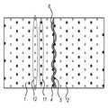
도 1은 종래기술의 일실시예에 따른 바이패스 다이오드 연결에 대한 스트립 컨덕터(strip conductor)를 가지는 두개의 인접한 광전지 셀 위에 가로놓인 후면 전극 레이어 파트(part)를 도시한 도면이다.
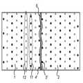
도 2는 본 발명의 일실시예에 따른 바이패스 다이오드 연결에 대한 스트립 컨덕터를 가지는 두개의 인접한 광전지 셀 위에 가로놓인 후면 전극 레이어 파트를 도시한 도면이다.
도 3은 본 발명의 일실시예에 따른 엣지 전극을 가지고 스트립을 수행하는 두개의 인접한 광전지 셀을 도시한 도면이다.
도 4는 본 발명의 다른 일실시예에 따른 엣지 전극을 가지고 스트립을 수행하는 두개의 인접한 광전지 셀을 도시한 도면이다.
도 5는 본 발명의 일실시예에 따른 들쑥날쑥하게 배치된(indented) 엣지 전극을 도시한 도면이다.FIG. 1 is a diagram illustrating a rear electrode layer part laid over two adjacent photovoltaic cells having a strip conductor for bypass diode connection according to one embodiment of the prior art.
2 illustrates a rear electrode layer part laid over two adjacent photovoltaic cells having a strip conductor for bypass diode connection according to one embodiment of the present invention.
3 illustrates two adjacent photovoltaic cells that perform strips with an edge electrode according to one embodiment of the present invention.
4 illustrates two adjacent photovoltaic cells that perform a strip with an edge electrode according to another embodiment of the present invention.
FIG. 5 is a view showing indented edge electrodes according to an embodiment of the present invention. FIG.
본 발명의 실시예들은 바이패스 다이오드를 이용하고 광전지 모듈(PV module)의 퍼포먼스(performance)를 향상시키는 회로와 연관된 복수의 광전지 셀(photovoltaic cell)을 가지는 광전지 모듈(photovoltaic module)에서의 향상된 레이아웃(lay-out) 및 후면 연결 시트의 배치에 관련될 수 있다.Embodiments of the present invention provide improved layouts in a photovoltaic module having a plurality of photovoltaic cells associated with circuits that utilize bypass diodes and enhance the performance of the photovoltaic modules. lay-out and placement of the rear connection sheet.
도 1은 (오직 엣지(7)만 표시된) 두개의 인접한 광전지 셀(PV cell)위에 가로놓인 후면 전극 레이어(3)(back side contact layer)의 파트(part)를 도시한 도면이다. 후면 전극 레이어(3)는 두개의 전극 레이어(contact layer) 파트(3) 사이에 위치한 스크라이브 레인(8)에 의해 분리된 바이패스 다이오드 연결(by-pass diode connection)에 대한 스트립 컨덕터(strip conductor) (6)을 포함할 수 있다. 일반적인 광전지 모듈(PV module)의 셋업(set-up)에서, 두개의 광전지 셀은 작은 대쉬 라인(dash line)(7a)에 의해 더 떨어져(1.75mm) 나타날 수도 있는 1.25mm의 공간(명목상, 솔리드 라인(solid line) 엣지(7) 사이)을 가지고 서로 인접하게 위치할 수 있다. 인접한 셀은 외부 엣지에 후면 전극 또는 도 1의 인접한 셀의 각각에 대한 외부 전극(4,5)이 있을 수 있다. 후면 전극 레이어(3)에서 바이패스 다이오드 컨덕터(by-pass diode conductor)(6)를 사용 가능한 공간에 맞추기 위해서, 바이패스 다이오드 컨덕터(6)은 오직 0.75mm의 일반적인 폭을 가질 수 있다. (효과적인 분리를 제공하기 위해서는 1mm의 넓은 스크라이브 레인(scribe lane)(8)이 필요한 것과 같이)1 shows a part of a back
두개의 셀(1,2)(도 3및 도 4 참조)이 인접하고 두개의 셀 모두 엣지를 따라 솔라셀(solar cell)의 후면에 전극을 가진다면, 셀(1,2)사이에 정션 박스(junction box)로 연장되는 구리 strip(바이패스 다이오드 컨덕터(6))을 위한 공간이 거의 없을 수 있다. 인접한 셀(1,2)의 전극(4,5) 사이의 공간은 작다. 또한, 스트립(6)을 만들기 위해서, 전극(4,5) 사이의 전도성 물질을 부식시키는 일반적으로 1mm의 분리된 스크라이브(8)가 필요할 수 있다. 이것은 일반적으로 9A의 전류를 흐르게 할 수 있는 아주 작은 스트립(6)으로 이끌 수 있고, 따라서 디바이스(device)에 유해할 수 있고 쉐이드 컨디션(shade condition) 아래 모듈 오퍼레이션(module operation)의 악영향을 가지는 높은 전력 손실을 유발할 수 있다.If two
아래의 계산의 예는 바이패스 다이오드를 위한 작은 구리 트랙(Cu track)을 위해 만들어질 수 있다. 바이패스 다이오드 컨덕터(6)를 위해 사용되는 일반적인 포일(foil)의 특성은 길이 l=0.5m; 두께 t=35μm, 간격 w=0.75mm 및 저항 R

이 문제는 일실시예들에 따른 본 발명의 제1 측면에서 해결될 수 있고, 미리 설정된 최소의 간격(w)을 가지는 바이패스 다이오드 연결 경로 (6)는 각각으로부터 셀간 거리에 위치하는 두개의 인접한 셀(1,2)의 엣지 방향을 따라 후면 연결 레이어 (3)에서 형성되고, 외부 전극 2d+s의 열(row) 사이의 총 거리가 미리 설정된 최소의 간격(w) 및 바이패스 다이오드 연결 경로(6)에 근접한 두개의 스크라이브 레인(scribe lane)의 폭(2i) 보다 크도록 각각의 인접한 셀에서 외부 전극(4,5)은 각각의 인접한 셀의 엣지로부터 거리(d)에 놓여진다. 수학적인 관점에서, 두개의 인접한 셀(1,2)의 외부 전극(4,5)의 거리(d)는
도 2에서, 이 문제에 대한 다른 해법은 미리 설정된 최소의 간격(w)을 가지는 바이패스 다이오드 연결 경로(6)가 후면 연결 레이어(3)에서 각각으로부터 셀간 거리(s)에 위치한 두개의 인접한 셀(1,2)의 가까운 엣지에 위치하는 외부 전극(4,5) 주위에 미엔더링 패턴(meandering pattern)을 가지는 인접한 셀(1,2)의 엣지 방향을 따라 형성되는 방법으로 제공된다. 이 실시예들에서, 거리(d)는 0일 수 있다. 즉, 외부 전극은 셀(1,2)의 엣지에서 직접 정렬될 수 있다. 이것은 결과적으로 셀(1,2)에 좀 더 최적의 전류 경로(current path)를 가지고, 셀에서의 적은 양의 금속 사용을 가져올 수 있다. (종종 이것은 은(Ag)이므로 비싸다.)Another solution to this problem is shown in Figure 2 where a bypass
좀 더 일반적으로, 복수의 셀(1,2)는 서브셋(subset)(4,5)가 인접한 셀 (1,2)를 따라 배열된 양극(positive) 후면 전극과 음극(negative) 후면 전극(11,12)의 대칭적인 패턴(symmetric pattern)을 가지는 셀을 포함할 수 있다. 셀(1,2)의 예는 IBC(Interdigitated Back Contact)셀 또는 EWT(Emitter Wrap Through)일 수 있다.More generally, the plurality of
다른 일실시예에서, 두개의 인접한 셀(1,2)은 외부 전극(4,5)이 상기 엣지 방향을 따라 산재(intersperse) 되도록 서로에 대하여 방향이 설정될 수 있다. 예를 들어, 두개의 인접한 셀(1,2)의 엣지 방향을 따라 길이 l을 가지는 광전지 셀(1,2)의 경우, 다수의 n 전극은 오프셋(offset) 0을 가지는 하나의 엣지 및 오프셋 l/2n 가지는 반대편 엣지에서 같은 거리에 위치할 수 있다. 이것은 n=4인 도 3에 더 명확하게 나타날 수 있다. 사용된 광전지 셀(1,2)의 후면 전극(11,12)은 후면 전극 광전지 셀에서 양극과 음극 모두 각각에 인접한 패턴으로 제공됨으로써 오픈 라운드(open round) 및 솔리드 라운드(solid round)를 사용함을 나타낼 수 있다. 광전지 모듈(PV module)에서, 위에 묘사된 광전지 셀(1,2)은 광전지 모듈 제조를 위한 쉬운 광전지 셀 배치를 허용하는 180도 회전에 대해 변하지 않을 수 있다.In another embodiment, the two
다른 일실시예에서, 양극 후면 전극과 음극 후면 전극(11,12)은 복수의 열(row)로 정렬될 수 있고, 외부 전극(4,5)을 포함하는 복수의 열 중 외부의 하나는 다른 열(11,12)들보다 전극을 적게 가질 수 있다. 이것은 바이패스 다이오드(바이패스 다이오드 컨덕터(6))를 위한 전도성 리드(conductive lead)의 더 부드러운 미엔더링(meandering)을 허용하고, 스크라이빙(scribing)에 의한 것과 같이 분리 레인(isolation lane)(8)들을 제공하는 후면 연결 레이어의 제조에 대한 이점들을 제공할 수 있다.In another embodiment, the anode back electrode and the
미엔더링 전도성 트랙(meandering conductive track)(6)의 인식 및 도 3에 보여지는 산재(intersperse) 방식으로 두개의 인접한 셀(1,2)의 엣지 전극(4,5)을 위치시킴으로 인해, 바이패스 다이오드(바이패스 다이오드 컨덕터(6))에 대한 전도성 리드(conductive lead)는 최고 2mm 또는 5mm의 간격을 가지는 종래 발명의 일실시예보다 더 넓은 간격을 가지는 것으로 인식될 수 있다. 이것은 두개의 인접한 셀 사이의 셀간 거리(s) 가 2mm보다 짧은 다른 일실시예와 결합될 수 있다. 이러한 해법은 하나의 광전지 모듈에 세개 이상의 바이패스 다이오드가 포함되는 것을 허용할 수 있다. 더 일반적으로, 본 발명은 복수의 광전지 셀(photovoltaic cell) 및 실시예들 중 하나에 따른 후면 연결 레이어를 포함하는 광전지 모듈(phothvoltaic module)과 연관있다.Due to the recognition of the meandering
일반적으로, 본 발명은 인접한 셀(1,2)의 엣지 전극(4,5) 사이에서 미엔더(meander)하는 구리 포일(Cu-foil)의 작은 스트립(strip)(6)을 포함하는 PCB와 같은 구리 포일(후면 연결 레이어(3))에 부착된 엣지를 따라 전극(4,5)과 후면 연결된 셀(1,2)의 배치와 연관될 수 있다. 다른 일실시예에서, 바이패스 다이오드 연결 경로(6)는 후면 연결 레이어(3)의 정션 박스 연결 부분(junction box connection part)으로 이어질 수 있다. 바이패스 연결 경로(6)는 전극(4,5)들이 바이패스 다이오드에 연결하고 전극(4,5)들이 광전지 모듈에 대한 일반적인 방식으로 바이패스 회로를 형성하는 정션 박스를 향해 늘어날 수 있다. 다른 방법으로 셀(1,2)들에 가까운 첫번째 셀 및 인접한 두번째 셀 아래에 있을 수 있는 각각의 셀(1,2)들의 엣지 전극(4,5)들 사이의 미엔더링(meandering) 경로(6)를 허용하면서, 두개의 인접한 셀(1,2)들의 전극(4,5)들은 산재(intersperse)될 수 있다.In general, the present invention relates to a PCB comprising a small strip of Cu foil meandering between the edge electrodes (4, 5) of adjacent cells (1, 2) May be associated with the placement of the electrodes (4,5) and the back-connected cells (1,2) along the edge attached to the same copper foil (back-connecting layer 3). In another embodiment, the bypass
도 4에 보여지는 다른 일실시예에서, 미엔더링 전도성 경로(6)는 셀(1,2)의 엣지 가까이에 위치한 서브셋(subset)(외부 전극(4`,5`))을 가지는 후면에 다수의 전류 콜렉션 포인트(current collection point)(11,12)를 가지는 후면 전극 셀(IBCs, EWTs)과 결합된 메탈 포일(metal foil)(3)에서 바이패스 다이오드 연결 목적을 위해 제공될 수 있다. 또는, 인접한 두개의 셀(1,2)의 외부 전극(4`,5`)은 셀(1,2)의 엣지로부터 떨어진 각각의 셀(1)의 중앙을 향해 들쑥날쑥하게 배치될(indented) 수 있다. 예를 들어, 이것은 도 5에 보여지듯이, 'elbow' 타입 또는 90도 배치 등과 같이 들쑥날쑥하게 배치된(indented) 버스바(busbar) 배치를 사용하여 수행될 수 있다. 여기에서, 전류 콜렉션 라인(current collection line)(15,18)은 콜렉션 버스바(14,17)와 함께 보여질 수 있다. 광전지 셀의 한쪽 면에서, 전극(12)은 제공될 수 있고, 다른 면에서는 다른 컨덕터(16)을 사용하여 전극(4)이 거리(d)를 넘어로 옮겨질 수 있다.In another embodiment, shown in FIG. 4, the meanderering
또는, 엣지 전극을 가지는 일반적인 광전지 셀(1,2)의 관점에서, 셀(1,2)의 엣지에 있는 외부 후면 전극(4`,5`)은 엣지에서 떨어진 셀(1,2)의 중앙으로 움직일 수 있다 (참조. 도 4의 외부 전극(4,5)과 도 3의 일실시예 비교). 본 일실시예에서, 좀 더 부드러운 미엔더링(meandering pattern)은 도 3의 일실시예보다 훨씬 큰 간격을 가지는 바이패스 다이오드 컨덕터(6)을 위해 사용될 수 있다.Alternatively, in view of the conventional
본 발명의 일실시예는 (셀의 대칭성에 의해 요구되는) 셀(1,2)의 엣지를 따라 위치한 전극(4,5)을 가지는 후면 전극 셀(1,2)을 위한 포일 기술(foil technology)의 어플리케이션을 허용하고, 표준 바이패스 회로가 통합될 수 있는 IBC셀 및 EWT셀을 포함하지만 IBC셀 및 EWT셀로 한정되지 않은 후면 전극 셀을 가지는 메탈 포일 베이스 광전지 모듈(metal foil-based PV module)을 인식하는 것을 허용할 수 있다.One embodiment of the present invention is a foil technology for the back electrode cell (1,2) having electrodes (4,5) located along the edge of the cell (1,2) (required by the symmetry of the cell) ), And a metal foil-based PV module having an IBC cell into which a standard bypass circuit can be integrated and a rear electrode cell including an EWT cell but not limited to an IBC cell and an EWT cell, As shown in FIG.
다른 일실시예에서, 후면 연결 레이어는 바이패스 다이오드뿐만 아니라 광전지 모듈의 인캡슐레이팅 레이어(encapsulating layer)에 의한 프로텍션(protection)을 허용하는 컨택팅 포일(contacting foil)(3)의 부분처럼 바이패스 다이오드 연결 경로(6)에 직접 연결된 바이패스 다이오드를 더 포함할 수 있다.In another embodiment, the backplane layer may include a bypass diode as well as a bypass diode, such as a portion of a contacting
본 발명의 실시예들은 도면에 보여지는 다수의 실시예들을 참조하여 설명될 수 있다. 수정 및 몇몇 부분 또는 구성요소의 대체 가능한 시행이 가능 하고, 첨부된 청구항에 정의된 보호범위에 포함될 수 있다.Embodiments of the present invention can be described with reference to a number of embodiments shown in the drawings. Modifications and substitutions of some parts or components are possible and may be included within the scope of protection defined in the appended claims.
1,2: 광전지 셀
3: 후면 연결 레이어1,2: photovoltaic cell
3: Rear connection layer
Claims (13)
Translated fromKorean광전지(photovoltaic) 모듈(module)을 형성하기 위해 복수의 광전지 셀(photovoltaic cell)들(1,2)의 양극(positive) 후면 전극(backside contact)과 음극(negative) 후면 전극(backside contact)(11,12)을 연결하고,
미리 설정된 최소의 간격(w)을 가지는 바이패스 다이오드(by-pass diode) 연결 경로(connection path)(6)는 각각으로부터 두개의 인접한 광전지 셀(1,2)의 엣지 방향을 따라 상기 후면 연결 레이어(back side connection layer)(3)에서 형성되고,
상기 두개의 인접한 광전지 셀은 각각으로부터 셀간 거리(s)에 위치하고,
상기 두개의 인접한 광전지 셀 각각의 외부 전극(outer contact)(4,5)은 각각의 상기 두개의 인접한 광전지 셀 각각의 엣지로부터 거리(d)만큼 떨어져 있고,
상기 거리(d)는 0보다 크고, 외부 전극들의 열(row) 간의 전체 길이(2d+s)는 상기 미리 설정된 최소 간격(w)과 바이패스 다이오드 연결 경로(6)에 인접한 두개의 스크라이브 레인들의 폭(2i)의 합보다 크거나 같은 후면 연결 레이어.In the back side connection layer,
A positive backside contact and a negative backside contact 11 of a plurality of photovoltaic cells 1 and 2 are formed to form a photovoltaic module. , 12) are connected,
A by-pass diode connection path 6 having a preset minimum spacing w is formed along the edge direction of two adjacent photovoltaic cells 1, 2 from each other, (back side connection layer) 3,
The two adjacent photovoltaic cells are located at an inter-cell distance s from each,
The outer contacts 4,5 of each of the two adjacent photovoltaic cells are spaced apart from the edges of each of the two adjacent photovoltaic cells by a distance d,
The distance d is greater than zero and the total length 2d + s between the rows of external electrodes is greater than the predetermined minimum spacing w and the width of the two scribe lanes adjacent to the bypass diode connection path 6. [ Rear connection layer that is greater than or equal to the sum of width (2i).
광전지(photovoltaic) 모듈(module) 형성을 위한 복수의 광전지 셀(photovoltaic cell)의 양극(positive) 후면 전극(backside contact)과 음극(negative) 후면 전극(11,12)을 연결하고,
미리 설정된 최소의 간격(w)을 가지는 바이패스 다이오드(by-pass diode) 연결 경로(connection path)(6)는 각각으로부터 두개의 인접한 광전지 셀(1,2)의 엣지 방향을 따라 외부 전극(4,5) 주위에 미엔더링 패턴(meandering pattern)으로 상기 후면 연결 레이어(back side connection layer)(3)에서 형성되고,
상기 두개의 인접한 광전지 셀은 각각으로부터 셀간 거리(s)에 위치하고,
상기 외부 전극(4,5)는 2개의 인접한 셀(1,2)의 엣지 가까이에 위치하는 후면 연결 레이어.In the back side connection layer,
A positive backside contact of a plurality of photovoltaic cells for forming a photovoltaic module is connected to negative backside electrodes 11 and 12,
A by-pass diode connection path 6 having a preset minimum interval w is connected to the external electrodes 4 and 5 along the edge directions of two adjacent photovoltaic cells 1 and 2 from each other. , 5) formed in the back side connection layer (3) in a meandering pattern,
The two adjacent photovoltaic cells are located at an inter-cell distance s from each,
Wherein the external electrodes (4,5) are located near the edges of two adjacent cells (1,2).
상기 2개의 인접한 광전지 셀은,
양극 후면 전극과 음극 후면 전극의 대칭 패턴을 가지는 셀들을 포함하고,
상기 양극 후면 전극과 음극 후면 전극의 서브셋은,
엣지 방향에 따라 정렬된 후면 연결 레이어.3. The method according to any one of claims 1 to 3,
Said two adjacent photovoltaic cells comprising:
A cell having symmetrical patterns of a cathode back electrode and a cathode back electrode,
And a subset of the cathode back electrode and the cathode back electrode,
Rear connection layer aligned in the edge direction.
상기 인접한 2개의 광전지 셀들(1,2)은,
엣지 방향에 따라 외부 전극(4,5)이 산재(intersperse) 되도록 서로에 대하여 방향이 설정된 후면 연결 레이어.4. The method according to any one of claims 1 to 3,
The two adjacent photovoltaic cells (1, 2)
And a rear connection layer oriented with respect to each other such that the external electrodes (4, 5) are interspersed along the edge direction.
상기 양극(positive) 후면 전극과 음극(negative) 후면 전극(11,12)은 복수의 열(row)들에서 정렬되고,
상기 복수의 행들 중 외부에 있는 어느 하나의 열은, 복수의 행들 중 다른 열에 있는 전극보다 적은 개수의 전극을 가지는 외부 전극을 포함하는 후면 연결 레이어.5. The method according to any one of claims 1 to 4,
The positive and negative backside electrodes 11 and 12 are aligned in a plurality of rows,
Wherein the outer one of the plurality of rows includes an outer electrode having a smaller number of electrodes than electrodes in the other of the plurality of rows.
상기 외부 전극(4,5)은 상기 셀(1,2)의 엣지에서 직접 정렬된 후면 연결 레이어.6. The method according to any one of claims 1 to 5,
The external electrodes (4, 5) are arranged directly on the edges of the cells (1, 2).
상기 인접한 셀(1,2)의 상기 외부 전극(4,5)은 각각의 셀(1)의 중심을 향해 들쑥날쑥하게 배치된(indented) 후면 연결 레이어.5. The method according to any one of claims 1 to 4,
Wherein the outer electrodes (4, 5) of the adjacent cells (1, 2) are indented towards the center of each cell (1).
상기 복수의 셀(1,2)는 IBC(Interdigitated Back Contact) 셀 또는 EWT(Emitter Wrap Through) 셀을 포함하는 후면 연결 레이어.8. The method according to any one of claims 1 to 7,
Wherein the plurality of cells (1,2) comprises an Interdigitated Back Contact (IBC) cell or an Emitter Wrap Through (EWT) cell.
상기 바이패스 다이오드 연결 경로(6)는 상기 후면 연결 레이어(3)의 정션 박스 연결 부분(junction box connection part)까지 이어지는 후면 연결 레이어.9. The method according to any one of claims 1 to 8,
The bypass diode connection path (6) leads to a junction box connection part of the rear connection layer (3).
상기 바이패스 다이오드 연결 경로(6)에 직접 연결된 바이패스 다이오드를 더 포함하는 후면 연결 레이어.9. The method according to any one of claims 1 to 8,
And a bypass diode directly connected to the bypass diode connection path (6).
상기 바이패스 다이오드 연결 경로(6)의 간격은 최소 2mm, 예를 들어 5mm인 후면 연결 레이어.11. The method according to any one of claims 1 to 10,
The spacing of the bypass diode connection paths 6 is at least 2 mm, for example 5 mm.
상기 인접한 두개의 광전지 셀들 간의 셀간 거리(s)는,
2mm보다 짧은 후면 연결 레이어.12. The method according to any one of claims 1 to 11,
The inter-cell distance (s) between the adjacent two photovoltaic cells may be expressed as:
Rear connection layer shorter than 2mm.
를 포함하는 광전지 모듈.A plurality of photovoltaic cells and a rear interconnect layer according to any one of claims 1 to 12
And a photovoltaic module.
Applications Claiming Priority (3)
| Application Number | Priority Date | Filing Date | Title |
|---|---|---|---|
| NL2012554ANL2012554B1 (en) | 2014-04-02 | 2014-04-02 | Back side contact layer for PV module with by-pass configuration. |
| NL2012554 | 2014-04-02 | ||
| PCT/EP2015/057021WO2015150382A1 (en) | 2014-04-02 | 2015-03-31 | Back side contact layer for pv module with by-pass configuration |
Publications (1)
| Publication Number | Publication Date |
|---|---|
| KR20160140770Atrue KR20160140770A (en) | 2016-12-07 |
Family
ID=51022991
Family Applications (1)
| Application Number | Title | Priority Date | Filing Date |
|---|---|---|---|
| KR1020167029464AWithdrawnKR20160140770A (en) | 2014-04-02 | 2015-03-31 | Back side contact layer for pv module with by-pass configuration |
Country Status (8)
| Country | Link |
|---|---|
| US (1) | US10056514B2 (en) |
| EP (1) | EP3127169B1 (en) |
| JP (1) | JP6618151B2 (en) |
| KR (1) | KR20160140770A (en) |
| CN (1) | CN106165118B (en) |
| NL (1) | NL2012554B1 (en) |
| TW (1) | TWI655785B (en) |
| WO (1) | WO2015150382A1 (en) |
Families Citing this family (2)
| Publication number | Priority date | Publication date | Assignee | Title |
|---|---|---|---|---|
| FR3131085A1 (en)* | 2021-12-20 | 2023-06-23 | Commissariat A L'energie Atomique Et Aux Energies Alternatives | THERMAL ACTIVATION PROCESS OF A PASSIVATION LAYER |
| CN114242810B (en)* | 2022-02-24 | 2022-04-29 | 广东爱旭科技有限公司 | Electrode structures, cells, assemblies, and battery systems for back-contact cells |
Family Cites Families (15)
| Publication number | Priority date | Publication date | Assignee | Title |
|---|---|---|---|---|
| US5972732A (en)* | 1997-12-19 | 1999-10-26 | Sandia Corporation | Method of monolithic module assembly |
| CN101548393A (en)* | 2005-07-26 | 2009-09-30 | 太阳能公司 | Method and system for manufacturing solar panels using an integrated solar cell using a plurality of photovoltaic regions |
| US20070095384A1 (en)* | 2005-10-28 | 2007-05-03 | Farquhar Donald S | Photovoltaic modules and interconnect methodology for fabricating the same |
| JP4989549B2 (en)* | 2007-08-24 | 2012-08-01 | 三洋電機株式会社 | Solar cell and solar cell module |
| WO2009134939A2 (en)* | 2008-04-29 | 2009-11-05 | Advent Solar, Inc. | Photovoltaic modules manufactured using monolithic module assembly techniques |
| US20100051085A1 (en)* | 2008-08-27 | 2010-03-04 | Weidman Timothy W | Back contact solar cell modules |
| NL2001958C (en)* | 2008-09-05 | 2010-03-15 | Stichting Energie | Method of monolithic photo-voltaic module assembly. |
| CN102318081A (en)* | 2009-02-13 | 2012-01-11 | 应用材料公司 | Low converging property flat distribution photovoltaic module |
| US20120081857A1 (en)* | 2009-06-25 | 2012-04-05 | Mitsubishi Electric Corporation | Terminal box for solar cell module |
| AT12234U1 (en)* | 2010-06-23 | 2012-01-15 | Austria Tech & System Tech | PHOTOVOLTAIC MODULE AND METHOD FOR PRODUCING A PHOTOVOLTAIC MODULE |
| CN103080447B (en) | 2010-06-23 | 2015-04-01 | 消防与安防五金有限公司 | A locking mechanism |
| NL2005261C2 (en)* | 2010-08-24 | 2012-02-27 | Solland Solar Cells B V | Back contacted photovoltaic cell with an improved shunt resistance. |
| NL2006932C2 (en)* | 2011-06-14 | 2012-12-17 | Stichting Energie | Photovoltaic cell. |
| JP2013048166A (en)* | 2011-08-29 | 2013-03-07 | Sharp Corp | Solar cell module, solar cell module array, and manufacturing method of solar cell module |
| WO2013182955A2 (en)* | 2012-06-05 | 2013-12-12 | Ebfoil S.R.L. | Back-sheet for photovoltaic modules comprising back-contact solar cells |
- 2014
- 2014-04-02NLNL2012554Apatent/NL2012554B1/ennot_activeIP Right Cessation
- 2015
- 2015-03-31KRKR1020167029464Apatent/KR20160140770A/ennot_activeWithdrawn
- 2015-03-31CNCN201580018822.5Apatent/CN106165118B/enactiveActive
- 2015-03-31WOPCT/EP2015/057021patent/WO2015150382A1/enactiveApplication Filing
- 2015-03-31JPJP2016560362Apatent/JP6618151B2/enactiveActive
- 2015-03-31EPEP15715998.9Apatent/EP3127169B1/enactiveActive
- 2015-03-31USUS15/300,289patent/US10056514B2/enactiveActive
- 2015-04-01TWTW104110696Apatent/TWI655785B/enactive
Also Published As
| Publication number | Publication date |
|---|---|
| NL2012554B1 (en) | 2016-02-15 |
| EP3127169A1 (en) | 2017-02-08 |
| NL2012554A (en) | 2016-01-12 |
| US10056514B2 (en) | 2018-08-21 |
| JP6618151B2 (en) | 2019-12-11 |
| TW201543700A (en) | 2015-11-16 |
| WO2015150382A1 (en) | 2015-10-08 |
| US20170186901A1 (en) | 2017-06-29 |
| TWI655785B (en) | 2019-04-01 |
| JP2017510082A (en) | 2017-04-06 |
| EP3127169B1 (en) | 2020-01-01 |
| CN106165118B (en) | 2018-06-01 |
| CN106165118A (en) | 2016-11-23 |
Similar Documents
| Publication | Publication Date | Title |
|---|---|---|
| KR101462699B1 (en) | Solar cell contact fingers and solder pad arrangement for enhanced efficiency | |
| WO2014096929A2 (en) | Photovoltaic cell element having a specific electrode configuration | |
| US11862745B2 (en) | One-dimensional metallization for solar cells | |
| TWI603493B (en) | Solar cell and its module | |
| ES2856075T3 (en) | Method for manufacturing a back contact solar cell solar module using linear tape type connector strips and the respective solar module | |
| CN104221159A (en) | Solar cell with metallization compensating for or preventing cracking | |
| US9685568B2 (en) | Photovoltaic module with flexible circuit | |
| US10714643B2 (en) | Back side contact layer for PV module with modified cell connection topology | |
| KR101691026B1 (en) | Solar cell and assembly of a plurality of solar cells | |
| KR101542003B1 (en) | Solar cell module | |
| KR20150145148A (en) | Solar cell module | |
| KR20160140770A (en) | Back side contact layer for pv module with by-pass configuration | |
| NL2015899B1 (en) | Interconnection of back-contacted solar cell, a solar panel having such interconnection. | |
| US20210280728A1 (en) | Photovoltaic module with back contact foil | |
| KR20150062792A (en) | Solar cell module and solar cell | |
| KR20150062788A (en) | Solar cell | |
| KR20160063130A (en) | Solar cell and solar cell module |
Legal Events
| Date | Code | Title | Description |
|---|---|---|---|
| PA0105 | International application | Patent event date:20161021 Patent event code:PA01051R01D Comment text:International Patent Application | |
| PG1501 | Laying open of application | ||
| A201 | Request for examination | ||
| PA0201 | Request for examination | Patent event code:PA02012R01D Patent event date:20200330 Comment text:Request for Examination of Application | |
| PC1202 | Submission of document of withdrawal before decision of registration | Comment text:[Withdrawal of Procedure relating to Patent, etc.] Withdrawal (Abandonment) Patent event code:PC12021R01D Patent event date:20200818 | |
| WITB | Written withdrawal of application |