KR20160140435A - Switch monitoring circuit - Google Patents
Switch monitoring circuitDownload PDFInfo
- Publication number
- KR20160140435A KR20160140435AKR1020160063580AKR20160063580AKR20160140435AKR 20160140435 AKR20160140435 AKR 20160140435AKR 1020160063580 AKR1020160063580 AKR 1020160063580AKR 20160063580 AKR20160063580 AKR 20160063580AKR 20160140435 AKR20160140435 AKR 20160140435A
- Authority
- KR
- South Korea
- Prior art keywords
- terminal
- voltage
- switch
- unit
- transistor
- Prior art date
- Legal status (The legal status is an assumption and is not a legal conclusion. Google has not performed a legal analysis and makes no representation as to the accuracy of the status listed.)
- Granted
Links
- 238000012544monitoring processMethods0.000titleclaimsabstractdescription98
- 238000001514detection methodMethods0.000claimsabstractdescription36
- 238000007599dischargingMethods0.000claimsabstractdescription5
- 238000000034methodMethods0.000claimsdescription6
- 239000003990capacitorSubstances0.000abstractdescription23
- 101100509369Caenorhabditis elegans isw-1 geneProteins0.000description10
- 238000010586diagramMethods0.000description8
- 230000004044responseEffects0.000description4
- 230000005669field effectEffects0.000description2
- 230000000694effectsEffects0.000description1
- 230000000087stabilizing effectEffects0.000description1
Images


Classifications
- G—PHYSICS
- G01—MEASURING; TESTING
- G01R—MEASURING ELECTRIC VARIABLES; MEASURING MAGNETIC VARIABLES
- G01R31/00—Arrangements for testing electric properties; Arrangements for locating electric faults; Arrangements for electrical testing characterised by what is being tested not provided for elsewhere
- G01R31/327—Testing of circuit interrupters, switches or circuit-breakers
- G01R31/3277—Testing of circuit interrupters, switches or circuit-breakers of low voltage devices, e.g. domestic or industrial devices, such as motor protections, relays, rotation switches
- B—PERFORMING OPERATIONS; TRANSPORTING
- B60—VEHICLES IN GENERAL
- B60R—VEHICLES, VEHICLE FITTINGS, OR VEHICLE PARTS, NOT OTHERWISE PROVIDED FOR
- B60R16/00—Electric or fluid circuits specially adapted for vehicles and not otherwise provided for; Arrangement of elements of electric or fluid circuits specially adapted for vehicles and not otherwise provided for
- B60R16/02—Electric or fluid circuits specially adapted for vehicles and not otherwise provided for; Arrangement of elements of electric or fluid circuits specially adapted for vehicles and not otherwise provided for electric constitutive elements
- B60R16/023—Electric or fluid circuits specially adapted for vehicles and not otherwise provided for; Arrangement of elements of electric or fluid circuits specially adapted for vehicles and not otherwise provided for electric constitutive elements for transmission of signals between vehicle parts or subsystems
- G—PHYSICS
- G01—MEASURING; TESTING
- G01R—MEASURING ELECTRIC VARIABLES; MEASURING MAGNETIC VARIABLES
- G01R1/00—Details of instruments or arrangements of the types included in groups G01R5/00 - G01R13/00 and G01R31/00
- G01R1/20—Modifications of basic electric elements for use in electric measuring instruments; Structural combinations of such elements with such instruments
- G01R1/203—Resistors used for electric measuring, e.g. decade resistors standards, resistors for comparators, series resistors, shunts
- G—PHYSICS
- G01—MEASURING; TESTING
- G01R—MEASURING ELECTRIC VARIABLES; MEASURING MAGNETIC VARIABLES
- G01R1/00—Details of instruments or arrangements of the types included in groups G01R5/00 - G01R13/00 and G01R31/00
- G01R1/20—Modifications of basic electric elements for use in electric measuring instruments; Structural combinations of such elements with such instruments
- G01R1/206—Switches for connection of measuring instruments or electric motors to measuring loads
- G—PHYSICS
- G01—MEASURING; TESTING
- G01R—MEASURING ELECTRIC VARIABLES; MEASURING MAGNETIC VARIABLES
- G01R15/00—Details of measuring arrangements of the types provided for in groups G01R17/00 - G01R29/00, G01R33/00 - G01R33/26 or G01R35/00
- G01R15/002—Switches for altering the measuring range or for multitesters
- G—PHYSICS
- G01—MEASURING; TESTING
- G01R—MEASURING ELECTRIC VARIABLES; MEASURING MAGNETIC VARIABLES
- G01R19/00—Arrangements for measuring currents or voltages or for indicating presence or sign thereof
- G01R19/165—Indicating that current or voltage is either above or below a predetermined value or within or outside a predetermined range of values
- G01R19/16504—Indicating that current or voltage is either above or below a predetermined value or within or outside a predetermined range of values characterised by the components employed
- G01R19/16523—Indicating that current or voltage is either above or below a predetermined value or within or outside a predetermined range of values characterised by the components employed using diodes, e.g. Zener diodes
- G—PHYSICS
- G01—MEASURING; TESTING
- G01R—MEASURING ELECTRIC VARIABLES; MEASURING MAGNETIC VARIABLES
- G01R31/00—Arrangements for testing electric properties; Arrangements for locating electric faults; Arrangements for electrical testing characterised by what is being tested not provided for elsewhere
- G01R31/005—Testing of electric installations on transport means
- G01R31/006—Testing of electric installations on transport means on road vehicles, e.g. automobiles or trucks
- H—ELECTRICITY
- H01—ELECTRIC ELEMENTS
- H01H—ELECTRIC SWITCHES; RELAYS; SELECTORS; EMERGENCY PROTECTIVE DEVICES
- H01H9/00—Details of switching devices, not covered by groups H01H1/00 - H01H7/00
- H01H9/16—Indicators for switching condition, e.g. "on" or "off"
- H01H9/167—Circuits for remote indication
Landscapes
- Physics & Mathematics (AREA)
- General Physics & Mathematics (AREA)
- Engineering & Computer Science (AREA)
- Computer Hardware Design (AREA)
- Microelectronics & Electronic Packaging (AREA)
- Mechanical Engineering (AREA)
- Chemical & Material Sciences (AREA)
- Combustion & Propulsion (AREA)
- Electronic Switches (AREA)
- Keying Circuit Devices (AREA)
- Direct Current Feeding And Distribution (AREA)
Abstract
Translated fromKoreanDescription
Translated fromKorean본 발명은 스위치 감시 회로에 관한 것으로, 특히 차량에 탑재되는 차재 장치를 구동시키기 위한 스위치의 상태를 감시하는 데에 적합한 스위치 감시 회로에 관한 것이다.BACKGROUND OF THE
자동차 등의 차량에서는, 이그니션이 오프의 상태여도, 윈도우의 개폐나 도어 미러의 개폐나 도어 로크의 시정·해정 등의 동작을 실시하는 경우가 있으며, 그에 대응하여, 파워 윈도우 장치나 도어 미러 개폐 장치나 도어 로크 장치 등의 차재 장치를 구동시키기 위한 스위치의 상태를 감시하고, 감시한 스위치의 상태를 차재 ECU (Engine Control Unit) 장치 등의 전자 기기에 전달하는 스위치 감시 회로가 실용화되어 있다.In a vehicle such as an automobile, even if the ignition is in the off state, there are cases where the opening and closing of the window, the opening and closing of the door mirror, and the locking and unlocking of the door lock are carried out. A switch monitoring circuit for monitoring the state of a switch for driving a vehicle-mounted device such as a door lock device and transmitting the monitored state of the switch to an electronic device such as an on-vehicle ECU (Engine Control Unit) is practically used.
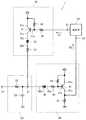
종래의 스위치 감시 회로에 관해서는 특허문헌 1 등이 개시되어 있다. 이하, 종래의 스위치 감시 회로의 구성에 대해 도 6 을 사용하여 설명한다. 도 6 은, 종래의 스위치 감시 회로 (101) 의 구성을 나타내는 설명도이다.
특허문헌 1 에 관련된 종래의 스위치 감시 회로 (101) 는, 도 6 에 나타내는 바와 같이, 스위치 (110) 에 접속된 회로이다. 스위치 (110) 는, 조작자의 조작에 대응하여 도어 미러 장치 등의 도시되지 않은 차재 장치를 구동시키기 위한 스위치이다. 스위치 감시 회로 (101) 는, 콘덴서 (112) 와, 전압 인가 수단 (120) 과, 마이크로 컴퓨터 (122) 등으로 이루어지는 제어 수단과, 입력 라인 (124) 등으로 이루어지는 전압 검출 수단과, 다이오드 (126) 를 구비하고 있다.The conventional
전압 인가 수단 (120) 은, 트랜지스터 (114) 와, 트랜지스터 (116) 와, 배터리 (118) 등을 가져 구성되는 스위칭 회로이고, 도시되지 않은 배선이나 커넥터 등을 개재하여 스위치 (110) 에 접속되어 있다. 전압 인가 수단 (120) 은, 마이크로 컴퓨터 (122) 로부터 출력되는 스트로브 펄스라고 불리는 제어 신호를 받아 기동되고, 스위치 (110) 에 전압을 인가하고 있다.The voltage applying means 120 is a switching circuit constituted by a
스위치 (110) 는 2 단자형 스위치이다. 스위치 (110) 의 일방의 단자는 다이오드 (126) 를 개재하여 전압 인가 수단 (120) 과 접속되고, 타방의 단자는 접지되어 있다. 그리고, 스위치 (110) 의 일방의 단자의 전압은, 전압 인가 수단 (120) 이 작동 중이고, 또한 스위치 (110) 가 열림 상태일 때에는 소정의 전압이 되고, 그 이외일 때에는 0 V 가 된다.The
마이크로 컴퓨터 (122) 는, 정기적으로 제어 신호를 전압 인가 수단 (120) 에 전달하여 전압 인가 수단 (120) 을 간헐 동작시키고 있다. 또, 마이크로 컴퓨터 (122) 는, 입력 라인 (124) 을 개재하여 스위치 (110) 의 일방의 단자의 전압을 모니터하고, 모니터한 전압에 기초하여 스위치 (110) 의 개폐 상태를 정기적으로 감시하고 있다. 또, 마이크로 컴퓨터 (122) 는, 도시되지 않은 배선 등을 개재하여 전술한 전자 기기에 접속되어 있고, 감시한 스위치 (110) 의 개폐 상태에 관한 정보를 차재 ECU (Engine Control Unit) 장치 등의 전자 기기에 전달하고 있다.The
이와 같은 스위치 감시 회로가 탑재되는 차량에서는, 차량의 배터리 잔량 유지 등의 관점에서, 암전류라고 불리는 이그니션이 오프의 상태일 때의 차량측의 소비 전류의 삭감이 항상 요구되고 있다. 또, 차량용으로서 사용되는 스위치나 커넥터의 접점의 도전성의 유지 등의 관점에서, 스위치 감시 회로와 스위치 사이에는 소정값 이상의 최저 전류를 흐르게 할 필요가 있었다.In a vehicle equipped with such a switch monitoring circuit, it is always required to reduce the current consumption on the vehicle side when the ignition, which is called the dark current, is in an OFF state, from the viewpoint of maintaining the remaining battery power of the vehicle. In addition, from the viewpoints of maintaining the conductivity of the contacts used for the vehicle or the contacts of the connector, it has been necessary to allow a minimum current exceeding a predetermined value to flow between the switch monitoring circuit and the switch.
그에 반해, 전술한 스위치 감시 회로 (101) 와 같은 회로에서는, 스위치 (110) 의 개폐 상태에 관계없이 전압 인가 수단 (120) 이 정기적으로 기동되고, 전압 인가 수단 (120) 의 동작에 수반하는 소비 전류가 암전류가 되므로, 암전류의 삭감을 저해하는 요인이 되고 있었다. 또, 암전류를 삭감시키기 위해 전압 인가 수단 (120) 의 소비 전류를 억제하면, 그에 맞추어 스위치 감시 회로 (101) 와 스위치 (110) 사이를 흐르는 전류도 적어져, 스위치 감시 회로 (101) 와 스위치 (110) 사이의 최저 전류를 유지할 수 없게 될 가능성이 있었다.On the other hand, in the circuit such as the above-described
본 발명은, 이와 같은 종래 기술의 실정을 감안하여 이루어진 것으로, 그 목적은, 암전류를 삭감시키기 쉽고, 또한 스위치 감시 회로와 스위치 사이의 최저 전류를 유지하기 쉬운 스위치 감시 회로를 제공하는 것에 있다.An object of the present invention is to provide a switch monitoring circuit which is easy to reduce the dark current and is easy to maintain the minimum current between the switch monitoring circuit and the switch.
이 과제를 해결하기 위해, 청구항 1 에 기재된 스위치 감시 회로는, 스위치에 접속되는 외부 입력 단자와, 상기 외부 입력 단자에 구동용 전압을 인가하는 구동 동작을 실시하는 전압 인가부와, 상기 외부 입력 단자의 전압의 변화를 검출하는 전압 검출부와, 상기 전압 인가부와 상기 전압 검출부에 접속된 제어부와, 상기 외부 입력 단자와 상기 전압 인가부에 접속된 축전부를 구비하고, 상기 축전부는, 상기 구동용 전압이 인가되는 전압 인가용 단자와, 일방의 단자가 상기 외부 입력 단자에 접속되고, 타방의 단자가 상기 전압 인가용 단자에 접속된 제 1 저항 소자와, 일방의 단자가 상기 전압 인가용 단자에 접속되고, 타방의 단자가 접지되어 상기 전압 인가용 단자로부터의 충전과 상기 전압 인가용 단자에 대한 방전을 실시하는 용량 소자를 갖고 있는 것을 특징으로 한다.In order to solve this problem, a switch monitoring circuit according to
이 구성에 의하면, 제어부가 전압 인가부와 전압 검출부에 접속되어 있으므로, 전압 검출부의 검출 결과에 기초하여 전압 인가부의 동작을 제어하고, 스위치가 조작되었을 때에 한정하여 전압 인가부에 구동 동작을 실시하게 할 수 있다. 그리고, 스위치가 조작되었을 때에 한정하여 전압 인가부에 구동 동작을 실시하게 함으로써, 전압 인가부의 동작 시간을 단축시킬 수 있어, 전압 인가부를 흐르는 암전류를 삭감시키기 쉬워진다. 게다가, 축전부는, 일방의 단자가 전압 인가용 단자에 접속되고, 타방의 단자가 접지되어 전압 인가용 단자로부터의 충전과 전압 인가용 단자에 대한 방전을 실시하는 용량 소자를 갖고 있으므로, 전압 인가부가 기동되고 나서 안정 동작할 때까지의 동안, 용량 소자의 방전에 의해 스위치 감시 회로로부터 스위치에 전류를 흐르게 할 수 있다. 또한, 축전부는, 일방의 단자가 외부 입력 단자에 접속되고, 타방의 단자가 전압 인가용 단자에 접속된 제 1 저항 소자를 갖고 있으므로, 용량 소자의 방전에 의해 스위치 감시 회로로부터 스위치에 흐르는 전류를 제 1 저항 소자에 의해 제한할 수 있고, 그것에 의해 스위치 감시 회로로부터 스위치에 흐르는 전류의 지속 시간을 길게 할 수 있다. 그 결과, 전압 인가부가 기동되고 나서 안정 동작할 때까지의 동안, 스위치 감시 회로로부터 스위치에 안정적으로 전류를 흐르게 할 수 있게 되어, 스위치 감시 회로와 스위치 사이의 최저 전류를 유지하기 쉬워진다.According to this configuration, since the control unit is connected to the voltage applying unit and the voltage detecting unit, the operation of the voltage applying unit is controlled based on the detection result of the voltage detecting unit, and the driving operation is performed on the voltage applying unit only when the switch is operated can do. By performing the driving operation on the voltage application unit only when the switch is operated, the operation time of the voltage application unit can be shortened and the dark current flowing in the voltage application unit can be easily reduced. In addition, since the power storage unit has a capacitive element in which one terminal is connected to the voltage applying terminal and the other terminal is grounded to charge from the voltage applying terminal and discharge to the voltage applying terminal, It is possible to cause a current to flow from the switch monitoring circuit to the switch by discharging the capacitive element from the start to the stable operation. The power storage unit has a first resistance element in which one terminal is connected to the external input terminal and the other terminal is connected to the voltage application terminal so that the current flowing from the switch monitoring circuit to the switch It can be limited by the first resistance element, whereby the duration of the current flowing from the switch monitoring circuit to the switch can be lengthened. As a result, it is possible to stably flow the current from the switch monitoring circuit to the switch during the period from when the voltage applying section is started to when the stabilizing operation is performed, so that it becomes easy to maintain the minimum current between the switch monitoring circuit and the switch.
청구항 2 에 기재된 스위치 감시 회로는, 상기 제어부는, 상기 스위치 감시 회로의 동작 상태를, 상기 전압 인가부가 상기 구동 동작을 실행하는 웨이크업 상태와, 상기 전압 인가부가 상기 구동 동작을 정지하는 슬립 상태로 전환 가능하고, 상기 전압 검출부의 검출 결과에 기초하여 상기 슬립 상태와 상기 웨이크업 상태의 전환을 실시하는 것을 특징으로 한다.The switch monitoring circuit according to claim 2 is characterized in that the control section controls the operation state of the switch monitoring circuit such that the voltage applying section is in a wakeup state in which the voltage applying section executes the drive operation and in a sleep state in which the voltage applying section stops the drive operation And switches between the sleep state and the wakeup state based on the detection result of the voltage detection section.
이 구성에 의하면, 제어부가 전압 검출부의 검출 결과에 기초하여 슬립 상태와 웨이크업 상태의 전환을 실시함으로써, 용이하게 전압 인가부가 구동 동작을 실시하는 시간을 스위치가 조작되었을 때에 한정할 수 있다. 그 결과, 암전류의 삭감이 더욱 용이해진다.According to this configuration, the control section switches the sleep state and the wakeup state based on the detection result of the voltage detection section, thereby making it possible to easily limit the time for the voltage application section to perform the drive operation when the switch is operated. As a result, the reduction of the dark current becomes easier.
청구항 3 에 기재된 스위치 감시 회로는, 상기 제어부는, 상기 용량 소자가 방전을 실시하고 있는 기간 내에 상기 슬립 상태에서 상기 웨이크업 상태로의 전환을 실시하고, 상기 전압 인가부에 상기 구동 동작을 개시하게 하는 것을 특징으로 한다.The switch monitoring circuit according to
이 구성에 의하면, 제어부가, 용량 소자가 방전을 실시하고 있는 기간 내에 슬립 상태에서 웨이크업 상태로의 전환을 실시하고, 전압 인가부에 구동 동작을 개시하게 하므로, 용량 소자의 방전에 의한 스위치 감시 회로로부터 스위치로의 전류와, 전압 인가부의 구동 동작에 의한 스위치 감시 회로로부터 스위치로의 전류의 전환이 원활해져, 스위치 감시 회로로부터 스위치로의 전류를 더욱 안정시킬 수 있다.According to this configuration, since the control section makes the switching from the sleep state to the wakeup state within the period in which the capacitive element discharges, and starts the driving operation to the voltage applying section, The current from the circuit to the switch and the current from the switch monitoring circuit to the switch due to the driving operation of the voltage applying section are smoothed and the current from the switch monitoring circuit to the switch can be further stabilized.
청구항 4 에 기재된 스위치 감시 회로는, 상기 제어부는, 상기 전압 인가부를 제어하기 위한 제어 단자를 갖고, 상기 전압 인가부는, 입력 단자와 전원 단자와 출력 단자를 갖는 제 1 트랜지스터와, 전류의 역류를 방지하기 위한 제 1 다이오드를 가져 구성되는 스위칭 회로이고, 상기 제 1 트랜지스터의 입력 단자는 상기 제어 단자에 접속되고, 상기 제 1 트랜지스터의 전원 단자는 전원에 접속되고, 상기 제 1 트랜지스터의 출력 단자는 상기 제 1 다이오드와 부하 저항이 되는 제 2 저항 소자를 개재하여 상기 전압 인가용 단자에 접속되어 있는 것을 특징으로 한다.The switch monitoring circuit according to claim 4, wherein the control unit has a control terminal for controlling the voltage applying unit, the voltage applying unit includes: a first transistor having an input terminal, a power supply terminal, and an output terminal; Wherein the input terminal of the first transistor is connected to the control terminal, the power terminal of the first transistor is connected to the power source, and the output terminal of the first transistor is connected to the power terminal of the first transistor, And is connected to the voltage applying terminal via a first diode and a second resistor element which becomes a load resistor.
이 구성에 의하면, 전압 인가부가 제 1 트랜지스터를 가져 구성되는 스위칭 회로이다. 이와 같은 스위칭 회로는 구성이 간단하므로, 전압 인가부의 구성을 간단하게 할 수 있다. 게다가, 제 1 트랜지스터의 출력 단자가 제 1 다이오드를 개재하여 전압 인가용 단자에 접속되어 있으므로, 축전부로부터 전압 인가부로의 전류의 역류를 방지할 수 있어, 스위치 감시 회로의 동작을 안정시키기 쉬워진다.According to this configuration, the voltage applying section is a switching circuit having the first transistor. Since such a switching circuit has a simple structure, the configuration of the voltage applying portion can be simplified. In addition, since the output terminal of the first transistor is connected to the voltage applying terminal via the first diode, the reverse flow of the current from the power storage unit to the voltage applying unit can be prevented, and the operation of the switch monitoring circuit can be stabilized easily .
청구항 5 에 기재된 스위치 감시 회로는, 상기 제어부는, 상기 전압 검출부를 모니터하기 위한 모니터 단자를 갖고, 상기 전압 검출부는, 입력 단자와 전원 단자와 출력 단자를 갖는 제 2 트랜지스터와, 전류의 역류를 방지하기 위한 제 2 다이오드를 가져 구성되는 스위칭 회로이고, 상기 제 2 트랜지스터의 입력 단자는 상기 제 2 다이오드를 개재하여 상기 전압 인가용 단자에 접속되고, 상기 제 2 트랜지스터의 전원 단자는 전원에 접속되고, 상기 제 2 트랜지스터의 출력 단자는 상기 모니터 단자에 접속됨과 함께, 부하 저항이 되는 제 3 저항 소자를 개재하여 접지되어 있는 것을 특징으로 한다.The switch monitoring circuit according to claim 5, wherein the control section has a monitor terminal for monitoring the voltage detecting section, the voltage detecting section includes: a second transistor having an input terminal, a power supply terminal, and an output terminal; The input terminal of the second transistor is connected to the voltage applying terminal via the second diode, the power terminal of the second transistor is connected to the power source, and the power source terminal of the second transistor is connected to the power source, And an output terminal of the second transistor is connected to the monitor terminal and is grounded via a third resistance element which becomes a load resistance.
이 구성에 의하면, 전압 검출부가 제 2 트랜지스터를 가져 구성되는 스위칭 회로이다. 이와 같은 스위칭 회로는 구성이 간단하므로, 전압 검출부의 구성을 간단하게 할 수 있다. 게다가, 제 2 트랜지스터의 입력 단자가 제 2 다이오드를 개재하여 전압 인가용 단자에 접속되어 있으므로, 축전부로부터 전압 검출부로의 전류의 역류를 방지할 수 있어, 스위치 감시 회로의 동작을 더욱 안정시키기 쉬워진다.According to this configuration, the voltage detecting unit is a switching circuit configured with the second transistor. Such a switching circuit has a simple structure, so that the configuration of the voltage detecting portion can be simplified. In addition, since the input terminal of the second transistor is connected to the voltage applying terminal via the second diode, it is possible to prevent the reverse flow of the current from the power storage unit to the voltage detecting unit, Loses.
청구항 6 에 기재된 스위치 감시 회로는, 상기 스위치는, 조작에 대응하여 서로의 개폐 상태가 변화하는 제 1 단자와 제 2 단자를 갖고, 상기 스위치의 제 1 단자는 상기 외부 입력 단자에 접속됨과 함께, 전류의 역류를 방지하기 위한 제 3 다이오드와 부하 저항이 되는 제 4 저항 소자를 개재하여 전원에 접속되고, 상기 스위치의 제 2 단자는 접지되어 있는 것을 특징으로 한다.The switch monitoring circuit according to claim 6 is characterized in that the switch has a first terminal and a second terminal, the open and closed states of which change according to the operation, the first terminal of the switch being connected to the external input terminal, A third diode for preventing reverse current flow and a fourth resistor element serving as a load resistor are connected to the power source, and the second terminal of the switch is grounded.
이 구성에 의하면, 스위치 감시 회로가 접속되는 스위치의 제 1 단자가 외부 입력 단자에 접속됨과 함께, 제 3 다이오드와 제 4 저항 소자를 개재하여 전원에 접속되어 있으므로, 전압 인가부의 회로 특성에 영향을 받지 않고, 비조작시의 외부 입력 단자의 전압을 설정할 수 있어, 용량 소자의 충전을 안정시키기 쉬워진다. 또, 스위치 감시 회로로부터 전원으로의 전류의 역류를 방지할 수 있어, 스위치 감시 회로의 동작을 안정시키기 쉬워진다. 또, 제 4 저항 소자의 양단의 전압을 스위치 감시 회로와 독립된 회로의 구동 등에 이용할 수 있어, 스위치의 기능을 다양화시키기 쉽다.According to this configuration, since the first terminal of the switch to which the switch monitoring circuit is connected is connected to the external input terminal and is connected to the power supply via the third diode and the fourth resistance element, The voltage of the external input terminal at the time of non-operation can be set, and the charging of the capacitive element can be easily stabilized. In addition, it is possible to prevent the reverse flow of the current from the switch monitoring circuit to the power source, thereby making it easy to stabilize the operation of the switch monitoring circuit. In addition, since the voltage at both ends of the fourth resistance element can be used for driving a circuit independent of the switch monitoring circuit, it is easy to diversify the function of the switch.
본 발명에 의하면, 암전류를 삭감시키기 쉽고, 또한 스위치 감시 회로와 스위치 사이의 최저 전류를 유지하기 쉬운 스위치 감시 회로를 제공할 수 있다.According to the present invention, it is possible to provide a switch monitoring circuit which is easy to reduce the dark current and is easy to maintain the minimum current between the switch monitoring circuit and the switch.
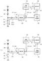
도 1 은, 본 발명의 실시형태에 관련된 스위치 감시 회로의 구성을 나타내는 회로도이다.
도 2 는, 본 발명의 실시형태에 관련된 전압 인가부와 전압 검출부의 구성을 나타내는 회로도이다.
도 3 은, 본 발명의 실시형태에 관련된 회로 동작을 나타내는 제 1 설명도이다.
도 4 는, 본 발명의 실시형태에 관련된 회로 동작을 나타내는 제 2 설명도이다.
도 5 는, 본 발명의 실시형태에 관련된 회로 동작에 관한 타이밍 차트이다.
도 6 은, 종래의 스위치 감시 회로의 구성을 나타내는 설명도이다.1 is a circuit diagram showing a configuration of a switch monitoring circuit according to an embodiment of the present invention.
2 is a circuit diagram showing the configuration of a voltage applying unit and a voltage detecting unit according to an embodiment of the present invention.
3 is a first explanatory diagram showing a circuit operation according to an embodiment of the present invention.
4 is a second explanatory diagram showing a circuit operation according to the embodiment of the present invention.
5 is a timing chart relating to the circuit operation according to the embodiment of the present invention.
Fig. 6 is an explanatory view showing a configuration of a conventional switch monitoring circuit.
이하, 본 발명의 실시형태에 대해 도 1 내지 도 6 을 참조하면서 설명한다. 도 1 은, 본 발명의 실시형태에 관련된 스위치 감시 회로 (1) 의 구성을 나타내는 회로도이다. 도 1 에서는, 스위치 감시 회로 (1) 와, 스위치 감시 회로 (1) 가 접속되는 스위치 (60) 의 구성을 나타내고 있다. 도 2 는, 본 발명의 실시형태에 관련된 전압 인가부 (30) 와 전압 검출부 (40) 의 구성을 나타내는 회로도이다. 도 3 은, 본 발명의 실시형태에 관련된 스위치 감시 회로 (1) 의 회로 동작을 나타내는 제 1 설명도이다. 도 3(a) 는 비조작시의 회로 동작을 나타내고, 도 3(b) 는 조작 개시 직후의 회로 동작을 나타내고 있다. 도 4 는, 본 발명의 실시형태에 관련된 스위치 감시 회로 (1) 의 회로 동작을 나타내는 제 2 설명도이다. 도 4(a) 는 안정 동작시의 회로 동작을 나타내고, 도 4(b) 는 조작 종료 직후의 회로 동작을 나타내고 있다. 도 5 는, 본 발명의 실시형태에 관련된 스위치 감시 회로 (1) 의 회로 동작에 관한 타이밍 차트이다. 도 5 에서는, 스위치 (60) 의 조작 타이밍과, 그에 수반하는 전압 인가부 (30) 의 동작 상태와, 외부 입력 단자 (10) 의 전압 (V1) 과, 전압 인가용 단자 (21) 의 전압 (V2) 과, 용량 소자 (23) 의 방전에 의해 스위치 감시 회로 (1) 로부터 스위치 (60) 에 흐르는 전류 (Isw1) 와, 전압 인가부 (30) 의 구동 동작에 의해 스위치 감시 회로 (1) 로부터 스위치 (60) 에 흐르는 전류 (Isw2) 와, 용량 소자 (23) 에 흘러드는 축전용 전류 (Ich) 의 변화를 나타내고 있다. 도 5 에 있어서 가로축은 시간이다.Hereinafter, an embodiment of the present invention will be described with reference to Figs. 1 to 6. Fig. 1 is a circuit diagram showing a configuration of a
먼저, 본 발명의 실시형태에 관련된 스위치 감시 회로 (1) 와, 스위치 감시 회로 (1) 가 접속되는 스위치 (60) 의 구성에 대해, 도 1 및 도 2 를 사용하여 설명한다. 본 발명의 실시형태에 관련된 스위치 감시 회로 (1) 는, 스위치 (60) 의 상태를 감시하기 위한 스위치 감시 회로이다. 스위치 (60) 는, 도시되지 않은 차량의 파워 윈도우 장치 등의 차재 장치를 구동시키기 위한 조작용 스위치이다.First, the
스위치 감시 회로 (1) 는, 도 1 에 나타내는 바와 같이, 외부 입력 단자 (10) 와, 축전부 (20) 와, 전압 인가부 (30) 와, 전압 검출부 (40) 와, 제어부 (50) 를 구비하고 있다. 외부 입력 단자 (10) 는, 스위치 (60) 에 접속되는 단자이다. 축전부 (20) 는, 구동용 전압이 인가되는 전압 인가용 단자 (21) 를 갖고 있다. 제어부 (50) 는 제어용 제어 단자 (51) 와, 모니터용 모니터 단자 (52) 를 갖고 있다.1, the
축전부 (20) 는, 외부 입력 단자 (10) 에 접속되는 축전용 RC 회로이고, 도 2 에 나타내는 바와 같이, 제 1 저항 소자 (22) 와 용량 소자 (23) 를 가져 구성된다. 제 1 저항 소자 (22) 는, 스위치 감시 회로 (1) 로부터 스위치 (60) 에 흐르는 전류를 제한하기 위한 저항이다. 제 1 저항 소자 (22) 의 일방의 단자는 외부 입력 단자 (10) 에 접속되어 있다. 제 1 저항 소자 (22) 의 타방의 단자는 전압 인가용 단자 (21) 에 접속되어 있다. 그리고, 전압 인가용 단자 (21) 에 인가된 구동용 전압이 제 1 저항 소자 (22) 를 개재하여 외부 입력 단자 (10) 에도 인가되도록 되어 있다. 용량 소자 (23) 는 축전용 용량 소자이고, 전해 콘덴서 등과 같은 수 ㎌ 이상의 용량의 것이 사용된다. 용량 소자 (23) 의 일방의 단자는 전압 인가용 단자 (21) 에 접속되어 있다. 용량 소자 (23) 의 타방의 단자는 접지되어 있다.The
전압 인가부 (30) 는, 외부 입력 단자 (10) 에 구동용 전압을 인가하는 구동 동작을 실시하기 위한 스위칭 회로이고, 도 2 에 나타내는 바와 같이, 제 1 트랜지스터 (31) 와 제 1 다이오드 (32) 를 가져 구성된다. 제 1 트랜지스터 (31) 는, PNP 형 바이폴러 트랜지스터이고, 전원 단자가 되는 이미터 단자 (31a) 와, 입력 단자가 되는 베이스 단자 (31b) 와, 출력 단자가 되는 콜렉터 단자 (31c) 를 갖고 있다. 제 1 다이오드 (32) 는, 축전부 (20) 로부터 전압 인가부 (30) 로의 전류의 역류를 방지하기 위한 다이오드이고, 애노드 단자 (32a) 와 캐소드 단자 (32b) 를 갖고 있다.The
제 1 트랜지스터 (31) 의 이미터 단자 (31a) 는 전원에 접속되어 있다. 제 1 트랜지스터 (31) 의 베이스 단자 (31b) 는, 제 5 저항 소자 (34) 를 개재하여 전원에 접속됨과 함께, 제 6 저항 소자 (35) 를 개재하여 제어부 (50) 의 제어 단자 (51) 에 접속되어 있다. 그리고, 제 1 트랜지스터 (31) 의 베이스 단자 (31b) 에는 제어부 (50) 의 제어 단자 (51) 로부터 제어용 신호인 제어 신호 (S1) 가 전달된다. 제 1 트랜지스터 (31) 의 콜렉터 단자 (31c) 는, 제 1 다이오드 (32) 의 애노드 단자 (32a) 에 접속되어 있다. 제 1 다이오드 (32) 의 캐소드 단자 (32b) 는, 부하 저항이 되는 제 2 저항 소자 (33) 를 개재하여 축전부 (20) 의 전압 인가용 단자 (21) 에 접속되어 있다. 그리고, 전압 인가부 (30) 는, 제어부 (50) 에 제어되어 구동 동작 (스위칭 동작) 을 실시하고, 축전부 (20) 를 개재하여 외부 입력 단자 (10) 에 전압을 인가하고 있다.The
전압 검출부 (40) 는, 외부 입력 단자 (10) 의 전압의 변화를 검출하기 위한 스위칭 회로이고, 도 2 에 나타내는 바와 같이, 제 2 트랜지스터 (41) 와 제 2 다이오드 (42) 를 가져 구성된다. 제 2 트랜지스터 (41) 는, PNP 형 바이폴러 트랜지스터이고, 전원 단자가 되는 이미터 단자 (41a) 와, 입력 단자가 되는 베이스 단자 (41b) 와, 출력 단자가 되는 콜렉터 단자 (41c) 를 갖고 있다. 제 2 다이오드 (42) 는, 축전부 (20) 로부터 전압 검출부 (40) 로의 전류의 역류를 방지하기 위한 다이오드이고, 애노드 단자 (42a) 와 캐소드 단자 (42b) 를 갖고 있다.The
제 2 트랜지스터 (41) 의 이미터 단자 (Q2a) 는 전원에 접속되어 있다. 제 2 트랜지스터 (41) 의 베이스 단자 (41b) 는, 제 7 저항 소자 (44) 를 개재하여 전원에 접속됨과 함께, 제 8 저항 소자 (45) 를 개재하여 제 2 다이오드 (42) 의 애노드 단자 (42a) 에 접속되어 있다. 제 2 트랜지스터 (41) 의 콜렉터 단자 (41c) 는, 제어부 (50) 의 모니터 단자 (52) 에 접속됨과 함께, 부하 저항이 되는 제 3 저항 소자 (43) 를 개재하여 접지되어 있다. 제 2 다이오드 (42) 의 캐소드 단자 (42b) 는, 축전부 (20) 의 전압 인가용 단자 (21) 에 접속되어 있다.And the emitter terminal Q2a of the
그리고, 전압 검출부 (40) 는, 외부 입력 단자 (10) 의 전압의 변화에 수반하는 전압 인가용 단자 (21) 의 전압의 변화에 대응하여 동작 (스위칭 동작) 하고, 외부 입력 단자 (10) 의 전압의 변화에 대응하여 전압이 변화하는 검출 신호 (S2) 를 출력하고 있다. 전압 검출부 (40) 가 출력한 검출 신호 (S2) 는, 제 2 트랜지스터 (41) 의 콜렉터 단자 (41c) 로부터 제어부 (50) 의 모니터 단자 (52) 에 전달된다.The
제어부 (50) 는, 전압 인가부 (30) 의 구동 동작을 제어하기 위한 제어 회로이고, 도시되지 않은 제어용 IC (집적 회로 소자) 등을 가져 구성된다. 제어부 (50) 는, 전압 검출부 (40) 로부터 제어부 (50) 의 모니터 단자 (52) 에 전달되는 검출 신호 (S2) 에 의해 전압 검출부 (40) 의 검출 결과를 모니터하고 있다. 또, 제어부 (50) 는, 제어부 (50) 의 제어 단자 (51) 로부터 전압 인가부 (30) 에 전달되는 제어 신호 (S1) 에 의해 전압 인가부 (30) 를 제어하고 있다. 그리고, 제어부 (50) 는, 전압 검출부 (40) 의 검출 결과에 기초하여 스위치 (60) 의 조작 상태에 관한 판단을 실시하고, 판단 결과에 기초하여 전압 인가부 (30) 의 구동 동작을 제어하고 있다. 본 실시형태에 있어서의 전압 인가부 (30) 의 구동 동작의 제어 방법은 이하와 같다.The
제어부 (50) 는, 전압 검출부 (40) 로부터 검출 신호 (S2) 가 전달되었을 때에 스위치 (60) 가 조작된 것으로 판단하고, 스위치 감시 회로 (1) 의 동작 상태를 전압 인가부 (30) 가 구동 동작을 실행하는 웨이크업 상태로 전환한다. 그리고, 전압 인가부 (30) 에 제어 신호 (S1) 가 전달되어 전압 인가부 (30) 가 기동되고, 전압 인가부 (30) 가 구동 동작을 실행한다. 또, 제어부 (50) 는, 전압 검출부 (40) 로부터 검출 신호 (S2) 가 전달되고 있지 않을 때에는, 스위치 (60) 가 비조작 상태인 것으로 판단하고, 스위치 감시 회로 (1) 의 동작 상태를 전압 인가부 (30) 가 구동 동작을 정지하는 슬립 상태로 전환한다. 그리고, 전압 인가부 (30) 로의 제어 신호 (S1) 의 전달이 정지하여, 전압 인가부 (30) 가 구동 동작을 정지한다. 제어부 (50) 는, 이와 같이 하여 전압 검출부 (40) 의 검출 결과에 기초하여 전압 인가부 (30) 의 구동 동작을 제어하고 있다.The
또, 제어부 (50) 는, 차재 ECU (Engine Control Unit) 장치 등의 도시되지 않은 차량의 전자 기기와도 접속되어 있으며, 검출 신호 (S2) 에 기초하는 판단 결과 등의 정보가 그 전자 기기에 전달된다. 그리고, 전달된 정보에 기초하여 파워 윈도우 장치 등의 차재 장치의 동작이 실행된다.The
스위치 (60) 는, 도 1 에 나타내는 바와 같이, 조작자의 조작에 대응하여 서로의 개폐 상태가 전환되는 제 1 단자 (61) 와 제 2 단자 (62) 를 갖는 2 단자형 스위치이다. 본 실시형태에서는, 스위치 (60) 가 조작되고 있지 않은 상태 (OFF 상태) 일 때에 제 1 단자 (61) 와 제 2 단자 (62) 가 열림 상태가 되고, 스위치 (60) 가 조작된 상태 (ON 상태) 일 때에 제 1 단자 (61) 와 제 2 단자 (62) 가 닫힘 상태가 된다.As shown in Fig. 1, the
또, 스위치 (60) 의 제 1 단자 (61) 는, 도시되지 않은 배선이나 커넥터 등을 개재하여 스위치 감시 회로 (1) 의 외부 입력 단자 (10) 에 접속됨과 함께, 제 3 다이오드 (63) 와 제 4 저항 소자 (64) 를 개재하여 전원에 접속되어 있다. 제 3 다이오드 (63) 는, 스위치 감시 회로 (1) 로부터 스위치 (60) 측의 전원으로의 전류의 역류를 방지하기 위한 다이오드이고, 애노드 단자 (63a) 와 캐소드 단자 (63b) 를 갖고 있다. 제 4 저항 소자 (64) 는, 부하 저항이 되는 저항 소자이다. 그리고, 제 3 다이오드 (63) 의 애노드 단자 (63a) 가 전원에 접속되고, 제 3 다이오드 (63) 의 캐소드 단자 (63b) 가 제 4 저항 소자 (64) 의 일방의 단자에 접속되고, 제 4 저항 소자 (64) 의 타방의 단자가 스위치 (60) 의 제 1 단자 (61) 에 접속되어 있다. 스위치 (60) 의 제 2 단자 (62) 는 접지되어 있다. 스위치 감시 회로 (1) 와 스위치 감시 회로 (1) 가 접속되는 스위치 (60) 는 이와 같은 구성으로 되어 있다.The
다음으로, 스위치 감시 회로 (1) 의 회로 동작에 대해, 도 3 내지 도 5 를 사용하여 설명한다. 이하의 설명에 있어서, 스위치 (60) 가 조작되고 있지 않을 때 (OFF 상태일 때) 를 비조작시로 하고, 스위치 (60) 가 조작되어 스위치 (60) 가 OFF 상태에서 ON 상태로 전환된 직후를 조작 개시 직후로 약칭하여 설명을 진행한다. 또, 스위치 (60) 가 조작되어 스위치 감시 회로 (1) 가 안정 동작하고 있을 때를 안정 동작시로 하고, 스위치 (60) 의 조작이 종료되어 스위치 (60) 가 ON 상태에서 OFF 상태로 전환된 직후를 조작 종료 직후로 약칭하여 설명을 진행한다.Next, the circuit operation of the
또, 도 3 내지 도 5 에 있어서, 전압 (V1) 은 외부 입력 단자 (10) 의 전압이고, 전압 (V2) 은 축전부 (20) 의 전압 인가용 단자 (21) 의 전압이다. 그리고, 각 단자의 전압은, 각 단자의 전위와 접지 전위 (0 V) 의 전위차를 의미하는 것으로 한다. 또, 각 단자의 전압이 저전압 상태가 된 상태를 Lo 상태라고 하고, 고전압 상태가 된 상태를 Hi 상태라고 한다. 또, 전류 (Isw) 는 용량 소자 (23) 의 방전 또는 전압 인가부 (30) 의 구동 동작에 의해 스위치 감시 회로 (1) 로부터 스위치 (60) 에 흐르는 전류이다. 그리고, 전류 (Isw1) 는 용량 소자 (23) 의 방전에 의해 스위치 감시 회로 (1) 로부터 스위치 (60) 에 흐르는 전류이고, 전류 (Isw2) 는 전압 인가부 (30) 의 구동 동작에 의해 스위치 감시 회로 (1) 로부터 스위치 (60) 에 흐르는 전류이다. 또, 전류 (Ich) 는 스위치 (60) 측의 전원으로부터 용량 소자 (23) 에 흘러드는 축전용 전류이다.3 to 5, the voltage V1 is the voltage of the
또, 도 5 에 있어서, 시간 (t1) 은 조작 개시 시간 (스위치 (60) 의 조작이 개시된 시간) 이다. 시간 (t2) 은 조작 개시에 수반하여 전압 인가부 (30) 가 구동 동작을 개시한 시간이다. 시간 (t3) 은 조작 개시에 수반하여 스위치 감시 회로 (1) 가 안정 동작 상태가 된 시간이다. 시간 (t4) 은 조작 종료 시간 (스위치 (60) 의 조작이 종료된 시간) 이다. 시간 (t5) 은 조작 종료에 수반하여 전압 인가부 (30) 가 구동 동작을 정지한 시간이다. 시간 (t6) 은 조작 종료에 수반하여 스위치 감시 회로 (1) 가 비조작시 상태로 되돌아온 시간이다.In Fig. 5, the time t1 is the operation start time (the time when the operation of the
먼저, 도 3(a) 및 도 5 (시간 (t1) 이전) 에 나타내는 바와 같이, 비조작시에는, 스위치 (60) 의 제 1 단자 (61) 와 제 2 단자 (62) 가 열림 상태가 되고, 외부 입력 단자 (10) 가 제 3 다이오드 (63) 와 제 4 저항 소자 (64) 를 개재하여 스위치 (60) 측의 전원에 접속된 상태로 되어 있다. 또, 축전부 (20) 의 용량 소자 (23) 는, 스위치 (60) 측의 전원으로부터 흘러든 전류에 의해 충전된 상태로 되어 있다. 그 결과, 전압 (V1) 과 전압 (V2) 은 모두 Hi 상태로 되어 있다. 또, 스위치 (60) 의 제 1 단자 (61) 와 제 2 단자 (62) 가 열림 상태이므로, 스위치 감시 회로 (1) 로부터 스위치 (60) 로의 전류 (Isw) 는 흐르지 않는다.First, as shown in Figs. 3A and 5 (before time t1), at the time of non-operation, the
다음으로, 도 3(b) 및 도 5 (시간 (t1) 에서 시간 (t2) 까지) 에 나타내는 바와 같이, 스위치 (60) 가 조작되면, 스위치 (60) 의 제 1 단자 (61) 와 제 2 단자 (62) 가 닫힘 상태가 되고, 외부 입력 단자 (10) 가 스위치 (60) 를 개재하여 접지된다. 그 결과, 전압 (V1) 은 Hi 상태에서 Lo 상태로 전환된다. 한편, 조작 개시 직후에는 용량 소자 (23) 가 축전된 상태인 채이므로, 전압 (V2) 은 Hi 상태로 되어 있다. 그리고, 용량 소자 (23) 의 방전에 의해 스위치 감시 회로 (1) 의 축전부 (20) 로부터 스위치 (60) 에 전류 (Isw1) 가 흐르고, 용량 소자 (23) 의 방전에 수반하여 전압 (V2) 이 서서히 저하된다. 또한, 전류 (Isw1) 가 흐를 때에는, 용량 소자 (23) 와 외부 입력 단자 (10) 사이에 개재되는 제 1 저항 소자 (22) 에 전류 (Isw1) 가 제한되므로, 전류 (Isw1) 의 지속 시간을 길게 할 수 있다.Next, as shown in Figs. 3 (b) and 5 (from time t1 to time t2), when the
다음으로, 도 4(a) 및 도 5 (시간 (t2) 에서 시간 (t4) 까지) 에 나타내는 바와 같이, 용량 소자 (23) 의 방전에 수반하여 전압 (V2) 이 저하되어 Lo 상태가 되면, 이 때의 전압 (V2) 의 변화에 맞추어 전압 검출부 (40) 가 동작을 개시하고, 전압 검출부 (40) 로부터 제어부 (50) 에 검출 신호 (S2) 가 전달된다. 그리고, 제어부 (50) 가 슬립 상태에서 웨이크업 상태로 전환되고, 전압 인가부 (30) 가 구동 조작을 개시한다. 그 결과, 전압 인가부 (30) 의 구동 동작에 의해 스위치 감시 회로 (1) 의 전압 인가부 (30) 로부터 스위치 (60) 에 전류 (Isw2) 가 안정적으로 흐르게 된다.Next, as shown in Fig. 4 (a) and Fig. 5 (from time t2 to time t4), when the voltage V2 drops to the Lo state with the discharge of the
다음으로, 도 4(b) 및 도 5 (시간 (t4) 에서 시간 (t6) 까지) 에 나타내는 바와 같이, 스위치 (60) 의 조작이 종료되면, 다시 스위치 (60) 의 제 1 단자 (61) 와 제 2 단자 (62) 가 열림 상태가 되고, 전류 (Isw) 가 흐르지 않게 된다. 또, 외부 입력 단자 (10) 가 제 3 다이오드 (63) 와 제 4 저항 소자 (64) 를 개재하여 다시 스위치 (60) 측의 전원에 접속되고, 전압 (V1) 이 Lo 상태에서 Hi 상태로 전환된다. 한편, 조작 종료 직후에는 용량 소자 (23) 가 충전되어 있지 않고, 전압 (V2) 은 Lo 상태로 되어 있지만, 스위치 (60) 측의 전원으로부터 축전부 (20) 에 축전용 전류 (Ich) 가 흘러들어, 용량 소자 (23) 에 대한 충전이 실시된다.Next, as shown in Figs. 4 (b) and 5 (from time t4 to time t6), when the operation of the
그리고, 용량 소자 (23) 에 대한 충전에 수반하여 전압 (V2) 이 서서히 높아져 Lo 상태에서 Hi 상태로 변화한다. 그리고, 이 때의 전압 (V2) 의 변화에 맞추어 전압 검출부 (40) 가 동작을 정지하고, 전압 검출부 (40) 로부터 제어부 (50) 에 검출 신호 (S2) 가 전달되지 않게 된다. 그리고, 제어부 (50) 가 웨이크업 상태에서 슬립 상태로 전환되고, 전압 인가부 (30) 가 구동 동작을 정지한다. 그 결과, 스위치 감시 회로 (1) 가 비조작시의 상태로 되돌아온다. 스위치 감시 회로 (1) 는, 스위치 (60) 의 조작에 대응하여 이와 같은 회로 동작을 실시하고 있다.Then, as the
다음으로, 본 실시형태의 효과에 대해 설명한다. 본 실시형태의 스위치 감시 회로 (1) 에서는, 제어부 (50) 가 전압 인가부 (30) 와 전압 검출부 (40) 에 접속되어 있으므로, 전압 검출부 (40) 의 검출 결과에 기초하여 전압 인가부 (30) 의 동작을 제어하고, 스위치 (60) 가 조작되었을 때에 한정하여 전압 인가부 (30) 에 구동 동작을 실시하게 할 수 있다. 그리고, 스위치 (60) 가 조작되었을 때에 한정하여 전압 인가부 (30) 에 구동 동작을 실시하게 함으로써, 전압 인가부 (30) 의 동작 시간을 단축시킬 수 있어, 전압 인가부 (30) 를 흐르는 암전류를 삭감시키기 쉬워진다.Next, the effect of the present embodiment will be described. Since the
게다가, 축전부 (20) 는, 일방의 단자가 전압 인가용 단자 (21) 에 접속되고, 타방의 단자가 접지되어 전압 인가용 단자 (21) 로부터의 충전과 전압 인가용 단자 (21) 에 대한 방전을 실시하는 용량 소자 (23) 를 갖고 있으므로, 전압 인가부 (30) 가 기동되고 나서 안정 동작할 때까지의 동안, 용량 소자 (23) 의 방전에 의해 스위치 감시 회로 (1) 로부터 스위치 (60) 에 전류를 흐르게 할 수 있다.In addition, the
또한, 축전부 (20) 는, 일방의 단자가 외부 입력 단자 (10) 에 접속되고, 타방의 단자가 전압 인가용 단자 (21) 에 접속된 제 1 저항 소자 (22) 를 갖고 있으므로, 용량 소자 (23) 의 방전에 의해 스위치 감시 회로 (1) 로부터 스위치 (60) 에 흐르는 전류 (Isw1) 를 제 1 저항 소자 (22) 에 의해 제한할 수 있고, 그것에 의해 전류 (Isw1) 의 지속 시간을 길게 할 수 있다. 그 결과, 전압 인가부 (30) 가 기동되고 나서 안정 동작할 때까지의 동안, 스위치 감시 회로 (1) 로부터 스위치 (60) 에 안정적으로 전류 (Isw) 를 흐르게 할 수 있게 되어, 스위치 감시 회로 (1) 와 스위치 (60) 사이의 최저 전류를 유지하기 쉬워진다.The
또, 본 실시형태의 스위치 감시 회로 (1) 에서는, 제어부 (50) 가 전압 검출부 (40) 의 검출 결과에 기초하여 슬립 상태와 웨이크업 상태의 전환을 실시함으로써, 용이하게 전압 인가부 (30) 가 구동 동작을 실시하는 시간을 스위치 (60) 가 조작되었을 때에 한정할 수 있다. 그 결과, 암전류의 삭감이 더욱 용이해진다.In the
또, 본 실시형태의 스위치 감시 회로 (1) 에서는, 제어부 (50) 가, 용량 소자 (23) 가 방전을 실시하고 있는 기간 내에 슬립 상태에서 웨이크업 상태로의 전환을 실시하고, 전압 인가부 (30) 에 구동 동작을 개시하게 하므로, 용량 소자 (23) 의 방전에 의한 스위치 감시 회로 (1) 로부터 스위치 (60) 로의 전류 (Isw1) 와, 전압 인가부 (30) 의 구동 동작에 의한 스위치 감시 회로 (1) 로부터 스위치 (60) 로의 전류 (Isw2) 의 전환이 원활해져, 스위치 감시 회로 (1) 로부터 스위치 (60) 로의 전류 (Isw) 를 더욱 안정시킬 수 있다.In the
또, 본 실시형태의 스위치 감시 회로 (1) 에서는, 전압 인가부 (30) 가 제 1 트랜지스터 (31) 를 가져 구성되는 스위칭 회로이다. 이와 같은 스위칭 회로는 구성이 간단하므로, 전압 인가부 (30) 의 구성을 간단하게 할 수 있다. 게다가, 제 1 트랜지스터 (31) 의 출력 단자가 되는 콜렉터 단자 (31c) 가 제 1 다이오드 (32) 를 개재하여 전압 인가용 단자 (21) 에 접속되어 있으므로, 축전부 (20) 로부터 전압 인가부 (30) 로의 전류의 역류를 방지할 수 있어, 스위치 감시 회로 (1) 의 동작을 안정시키기 쉬워진다.In the
또, 본 실시형태의 스위치 감시 회로 (1) 에서는, 전압 검출부 (40) 가 제 2 트랜지스터 (41) 를 가져 구성되는 스위칭 회로이다. 이와 같은 스위칭 회로는 구성이 간단하므로, 전압 검출부 (40) 의 구성을 간단하게 할 수 있다. 게다가, 제 2 트랜지스터 (41) 의 입력 단자가 되는 베이스 단자 (41b) 가 제 2 다이오드 (42) 를 개재하여 전압 인가용 단자 (21) 에 접속되어 있으므로, 축전부 (20) 로부터 전압 검출부 (40) 로의 전류의 역류를 방지할 수 있어, 스위치 감시 회로 (1) 의 동작을 더욱 안정시키기 쉬워진다.In the
또, 본 실시형태의 스위치 감시 회로 (1) 에서는, 스위치 감시 회로 (1) 가 접속되는 스위치 (60) 의 제 1 단자 (61) 가 외부 입력 단자 (10) 에 접속됨과 함께, 제 3 다이오드 (63) 와 제 4 저항 소자 (64) 를 개재하여 전원에 접속되어 있으므로, 전압 인가부 (30) 의 회로 특성에 영향을 받지 않고, 비조작시의 외부 입력 단자 (10) 의 전압을 설정할 수 있어, 용량 소자 (23) 의 충전을 안정시키기 쉬워진다. 또, 스위치 감시 회로 (1) 로부터 전원으로의 전류의 역류를 방지할 수 있어, 스위치 감시 회로 (1) 의 동작을 안정시키기 쉬워진다. 또, 제 4 저항 소자 (64) 의 양단의 전압을 스위치 감시 회로 (1) 와 독립된 회로의 구동 등에 이용할 수 있어, 스위치의 기능을 다양화시키기 쉽다.In the
이상, 본 발명의 실시형태에 대해 설명해 왔으나, 본 발명은 상기의 실시형태에 한정되지 않고, 본 발명의 요지를 일탈하지 않는 한에 있어서 적절히 변경할 수 있다.Although the embodiments of the present invention have been described above, the present invention is not limited to the above-described embodiments and can be appropriately changed without departing from the gist of the present invention.
예를 들어, 본 발명의 실시형태에 있어서, 축전부 (20) 의 제 1 저항 소자 (22) 의 타방의 단자와 전압 인가용 단자 (21) 를 저항 소자 등을 개재하여 접속시켜도 상관없다. 또, 축전부 (20) 는, 전압 인가용 단자 (21) 와는 별도로 전압 검출부 (40) 가 접속되는 전압 검출용 단자를 갖고 있어도 상관없다.For example, in the embodiment of the present invention, the other terminal of the
또, 본 발명의 실시형태에 있어서, 전압 인가부 (30) 를 NPN 형 바이폴러 트랜지스터나 전계 효과 트랜지스터나 IC (집적 회로) 등을 사용하여 구성해도 상관없다. 또, 제 1 트랜지스터 (31) 가 저항 내장형 트랜지스터인 경우에는, 제 5 저항 소자 (34) 와 제 6 저항 소자 (35) 는 없어도 상관없다. 또, 축전부 (20) 로부터 전압 인가부 (30) 로의 전류의 역류의 영향이 없는 것이면, 제 1 다이오드 (32) 는 없어도 상관없다. 또, 제 2 저항 소자 (33) 의 기능을 제 1 저항 소자 (22) 등의 다른 저항 소자에 의해 대용할 수 있는 경우에는, 제 2 저항 소자 (33) 는 없어도 상관없다.In the embodiment of the present invention, the
또, 본 발명의 실시형태에 있어서, 전압 검출부 (40) 를 NPN 형 바이폴러 트랜지스터나 전계 효과 트랜지스터나 IC (집적 회로) 등을 사용하여 구성해도 상관없다. 또, 제 2 트랜지스터 (41) 가 저항 내장형 트랜지스터인 경우에는, 제 7 저항 소자 (44) 와 제 8 저항 소자 (45) 는 없어도 상관없다. 또, 축전부 (20) 로부터 전압 검출부 (40) 로의 전류의 역류의 영향이 없는 것이면, 제 2 다이오드 (42) 는 없어도 상관없다.In the embodiment of the present invention, the
또, 본 발명의 실시형태에 있어서, 제어부 (50) 는 전술한 이외의 제어 동작을 실시해도 상관없고, 제어 동작 이외에 연산 등의 동작을 실시해도 상관없다.In the embodiment of the present invention, the
또, 본 발명의 실시형태에 있어서, 또, 스위치 감시 회로 (1) 가 접속되는 스위치 (60) 는, 3 단자형 스위치나 그 이외의 스위치여도 상관없다. 또, 스위치 (60) 에는 추가로 다른 회로가 접속되어 있어도 상관없다.Further, in the embodiment of the present invention, the
또, 본 발명의 실시형태에 있어서, 스위치 감시 회로 (1) 는 전술한 이외의 회로나 기능을 추가로 구비하고 있어도 상관없다. 예를 들어, 전압 인가부 (30) 가 인가하는 구동용 전압을 이용하여 용량 소자 (23) 에 대한 충전을 실시해도 상관없다. 그 경우, 스위치 (60) 는 제 3 다이오드 (63) 와 제 4 저항 소자 (64) 를 개재하여 전원에 접속되어 있지 않아도 상관없다.In addition, in the embodiment of the present invention, the
1 : 스위치 감시 회로
10 : 입력 단자
20 : 축전부
21 : 전압 인가용 단자
22 : 제 1 저항 소자
23 : 용량 소자
30 : 전압 인가부
31 : 제 1 트랜지스터
31a : 이미터 단자
31b : 베이스 단자
31c : 콜렉터 단자
32 : 제 1 다이오드
32a : 애노드 단자
32b : 캐소드 단자
33 : 제 2 저항 소자
34 : 제 5 저항 소자
35 : 제 6 저항 소자
40 : 전압 검출부
41 : 제 2 트랜지스터
41a : 이미터 단자
41b : 베이스 단자
41c : 콜렉터 단자
42 : 제 2 다이오드
42a : 애노드 단자
42b : 캐소드 단자
43 : 제 3 저항 소자
44 : 제 7 저항 소자
45 : 제 8 저항 소자
50 : 제어부
51 : 제어 단자
52 : 모니터 단자
60 : 스위치
61 : 제 1 단자
62 : 제 2 단자
63 : 제 3 다이오드
63a : 애노드 단자
63b : 캐소드 단자
64 : 제 4 저항 소자1: Switch monitoring circuit
10: Input terminal
20:
21: Terminal for voltage application
22: first resistance element
23: Capacitive element
30:
31: first transistor
31a: Emitter terminal
31b: base terminal
31c: Collector terminal
32: first diode
32a: anode terminal
32b: cathode terminal
33: second resistance element
34: fifth resistor element
35: sixth resistance element
40: Voltage detector
41: second transistor
41a: Emitter terminal
41b: base terminal
41c: Collector terminal
42: second diode
42a: anode terminal
42b: cathode terminal
43: third resistance element
44: Resistor element 7
45: Eighth resistor element
50:
51: Control terminal
52: Monitor terminal
60: Switch
61: first terminal
62: second terminal
63: third diode
63a: anode terminal
63b: cathode terminal
64: fourth resistance element
Claims (6)
Translated fromKorean상기 외부 입력 단자에 구동용 전압을 인가하는 구동 동작을 실시하는 전압 인가부와,
상기 외부 입력 단자의 전압의 변화를 검출하는 전압 검출부와,
상기 전압 인가부와 상기 전압 검출부에 접속된 제어부와,
상기 외부 입력 단자와 상기 전압 인가부에 접속된 축전부를 구비하고,
상기 축전부는,
상기 구동용 전압이 인가되는 전압 인가용 단자와,
일방의 단자가 상기 외부 입력 단자에 접속되고, 타방의 단자가 상기 전압 인가용 단자에 접속된 제 1 저항 소자와,
일방의 단자가 상기 전압 인가용 단자에 접속되고, 타방의 단자가 접지되어 상기 전압 인가용 단자로부터의 충전과 상기 전압 인가용 단자에 대한 방전을 실시하는 용량 소자를 갖고 있는 것을 특징으로 하는 스위치 감시 회로.An external input terminal connected to the switch,
A voltage applying unit for applying a driving voltage to the external input terminal,
A voltage detector for detecting a change in the voltage of the external input terminal;
A control unit connected to the voltage application unit and the voltage detection unit,
And a power storage unit connected to the external input terminal and the voltage applying unit,
The power storage unit includes:
A voltage applying terminal to which the driving voltage is applied,
A first resistor element having one terminal connected to the external input terminal and the other terminal connected to the voltage applying terminal,
And a capacitive element for charging one of the voltage application terminals and discharging the voltage application terminal, wherein one terminal is connected to the voltage application terminal and the other terminal is grounded to charge the voltage application terminal and discharge the voltage application terminal. Circuit.
상기 제어부는, 상기 스위치 감시 회로의 동작 상태를, 상기 전압 인가부가 상기 구동 동작을 실행하는 웨이크업 상태와, 상기 전압 인가부가 상기 구동 동작을 정지하는 슬립 상태로 전환 가능하고, 상기 전압 검출부의 검출 결과에 기초하여 상기 슬립 상태와 상기 웨이크업 상태의 전환을 실시하는 것을 특징으로 하는 스위치 감시 회로.The method according to claim 1,
Wherein the control unit switches the operation state of the switch monitoring circuit to a wakeup state in which the voltage application unit executes the drive operation and a sleep state in which the voltage application unit stops the drive operation, And switches the sleep state and the wakeup state based on a result of the comparison.
상기 제어부는, 상기 용량 소자가 방전을 실시하고 있는 기간 내에, 상기 슬립 상태에서 상기 웨이크업 상태로의 전환을 실시하고, 상기 전압 인가부에 상기 구동 동작을 개시하게 하는 것을 특징으로 하는 스위치 감시 회로.3. The method of claim 2,
Wherein the control unit switches the state from the sleep state to the wakeup state within a period in which the capacitive element discharges and causes the voltage applying unit to start the driving operation. .
상기 제어부는, 상기 전압 인가부를 제어하기 위한 제어 단자를 갖고,
상기 전압 인가부는, 입력 단자와 전원 단자와 출력 단자를 갖는 제 1 트랜지스터와, 전류의 역류를 방지하기 위한 제 1 다이오드를 가져 구성되는 스위칭 회로이고,
상기 제 1 트랜지스터의 입력 단자는 상기 제어 단자에 접속되고,
상기 제 1 트랜지스터의 전원 단자는 전원에 접속되고,
상기 제 1 트랜지스터의 출력 단자는 상기 제 1 다이오드와 부하 저항이 되는 제 2 저항 소자를 개재하여 상기 전압 인가용 단자에 접속되어 있는 것을 특징으로 하는 스위치 감시 회로.The method of claim 3,
Wherein the control unit has a control terminal for controlling the voltage applying unit,
The voltage application unit is a switching circuit having a first transistor having an input terminal, a power supply terminal, and an output terminal, and a first diode for preventing reverse current flow,
An input terminal of the first transistor is connected to the control terminal,
A power source terminal of the first transistor is connected to a power source,
And the output terminal of the first transistor is connected to the voltage applying terminal via the first diode and a second resistor element which becomes a load resistor.
상기 제어부는, 상기 전압 검출부를 모니터하기 위한 모니터 단자를 갖고,
상기 전압 검출부는, 입력 단자와 전원 단자와 출력 단자를 갖는 제 2 트랜지스터와, 전류의 역류를 방지하기 위한 제 2 다이오드를 가져 구성되는 스위칭 회로이고,
상기 제 2 트랜지스터의 입력 단자는 상기 제 2 다이오드를 개재하여 상기 전압 인가용 단자에 접속되고,
상기 제 2 트랜지스터의 전원 단자는 전원에 접속되고,
상기 제 2 트랜지스터의 출력 단자는 상기 모니터 단자에 접속됨과 함께, 부하 저항이 되는 제 3 저항 소자를 개재하여 접지되어 있는 것을 특징으로 하는 스위치 감시 회로.5. The method of claim 4,
Wherein the control unit has a monitor terminal for monitoring the voltage detection unit,
Wherein the voltage detection unit is a switching circuit having a second transistor having an input terminal, a power supply terminal and an output terminal, and a second diode for preventing a reverse current of the current,
An input terminal of the second transistor is connected to the voltage applying terminal via the second diode,
A power source terminal of the second transistor is connected to a power source,
Wherein an output terminal of the second transistor is connected to the monitor terminal and is grounded via a third resistance element which becomes a load resistance.
상기 스위치는, 조작에 대응하여 서로의 개폐 상태가 변화하는 제 1 단자와 제 2 단자를 갖고,
상기 스위치의 제 1 단자는 상기 외부 입력 단자에 접속됨과 함께, 전류의 역류를 방지하기 위한 제 3 다이오드와 부하 저항이 되는 제 4 저항 소자를 개재하여 전원에 접속되고,
상기 스위치의 제 2 단자는 접지되어 있는 것을 특징으로 하는 스위치 감시 회로.6. The method of claim 5,
Wherein the switch has a first terminal and a second terminal, the open and closed states of which change according to the operation,
A first terminal of the switch is connected to the external input terminal and is connected to a power source via a third diode for preventing reverse current flow and a fourth resistor element serving as a load resistor,
And the second terminal of the switch is grounded.
Applications Claiming Priority (2)
| Application Number | Priority Date | Filing Date | Title |
|---|---|---|---|
| JP2015110540AJP6493874B2 (en) | 2015-05-29 | 2015-05-29 | Switch monitoring circuit |
| JPJP-P-2015-110540 | 2015-05-29 |
Publications (2)
| Publication Number | Publication Date |
|---|---|
| KR20160140435Atrue KR20160140435A (en) | 2016-12-07 |
| KR101714320B1 KR101714320B1 (en) | 2017-03-08 |
Family
ID=55802250
Family Applications (1)
| Application Number | Title | Priority Date | Filing Date |
|---|---|---|---|
| KR1020160063580AActiveKR101714320B1 (en) | 2015-05-29 | 2016-05-24 | Switch monitoring circuit |
Country Status (4)
| Country | Link |
|---|---|
| US (1) | US9783139B2 (en) |
| EP (1) | EP3098826B1 (en) |
| JP (1) | JP6493874B2 (en) |
| KR (1) | KR101714320B1 (en) |
Cited By (1)
| Publication number | Priority date | Publication date | Assignee | Title |
|---|---|---|---|---|
| US20190391549A1 (en)* | 2018-06-20 | 2019-12-26 | Pilz Gmbh & Co. Kg | Circuit Arrangement for Switching an Electrical Load and Method for Checking a Status of a Safety Output of a Circuit Arrangement |
Families Citing this family (2)
| Publication number | Priority date | Publication date | Assignee | Title |
|---|---|---|---|---|
| DE102016105544A1 (en)* | 2016-03-24 | 2017-09-28 | Epcos Ag | Apparatus for measuring a state of an electrical switch, electrical switch and method for measuring a state of an electrical switch |
| JP6487882B2 (en)* | 2016-08-12 | 2019-03-20 | ミネベアミツミ株式会社 | Address control circuit and control method of address control circuit |
Citations (3)
| Publication number | Priority date | Publication date | Assignee | Title |
|---|---|---|---|---|
| JPH01303053A (en)* | 1988-01-29 | 1989-12-06 | Stanley Electric Co Ltd | Low voltage detection circuit |
| JP2005160166A (en) | 2003-11-21 | 2005-06-16 | Yazaki Corp | Switch monitoring circuit |
| JP2010166110A (en)* | 2009-01-13 | 2010-07-29 | Seiko Instruments Inc | Voltage detection circuit |
Family Cites Families (10)
| Publication number | Priority date | Publication date | Assignee | Title |
|---|---|---|---|---|
| JPH0865753A (en)* | 1994-08-19 | 1996-03-08 | Sumitomo Wiring Syst Ltd | Current limiting circuit for switch |
| US5621250A (en)* | 1995-07-31 | 1997-04-15 | Ford Motor Company | Wake-up interface and method for awakening an automotive electronics module |
| JP3524294B2 (en)* | 1996-10-14 | 2004-05-10 | アルプス電気株式会社 | Switch open / closed state detection circuit |
| JP2001216878A (en)* | 2000-02-03 | 2001-08-10 | Toyota Motor Corp | Switch status monitoring circuit and switch |
| JP3774360B2 (en)* | 2000-09-26 | 2006-05-10 | アルプス電気株式会社 | Wake-up start-up circuit |
| US7561386B2 (en)* | 2005-10-24 | 2009-07-14 | Yazaki Corporation | Switch monitoring circuit |
| US8841799B2 (en)* | 2009-04-29 | 2014-09-23 | Bose Corporation | Zero power drain pushbutton controls |
| JP5463836B2 (en)* | 2009-10-02 | 2014-04-09 | 株式会社オートネットワーク技術研究所 | Processing system |
| US9541604B2 (en)* | 2013-04-29 | 2017-01-10 | Ge Intelligent Platforms, Inc. | Loop powered isolated contact input circuit and method for operating the same |
| US9465075B2 (en)* | 2014-08-29 | 2016-10-11 | Freescale Semiconductor, Inc. | Wetting current diagnostics |
- 2015
- 2015-05-29JPJP2015110540Apatent/JP6493874B2/enactiveActive
- 2016
- 2016-04-19EPEP16165903.2Apatent/EP3098826B1/enactiveActive
- 2016-05-03USUS15/145,244patent/US9783139B2/enactiveActive
- 2016-05-24KRKR1020160063580Apatent/KR101714320B1/enactiveActive
Patent Citations (3)
| Publication number | Priority date | Publication date | Assignee | Title |
|---|---|---|---|---|
| JPH01303053A (en)* | 1988-01-29 | 1989-12-06 | Stanley Electric Co Ltd | Low voltage detection circuit |
| JP2005160166A (en) | 2003-11-21 | 2005-06-16 | Yazaki Corp | Switch monitoring circuit |
| JP2010166110A (en)* | 2009-01-13 | 2010-07-29 | Seiko Instruments Inc | Voltage detection circuit |
Cited By (2)
| Publication number | Priority date | Publication date | Assignee | Title |
|---|---|---|---|---|
| US20190391549A1 (en)* | 2018-06-20 | 2019-12-26 | Pilz Gmbh & Co. Kg | Circuit Arrangement for Switching an Electrical Load and Method for Checking a Status of a Safety Output of a Circuit Arrangement |
| US11619919B2 (en)* | 2018-06-20 | 2023-04-04 | Pilz Gmbh & Co. Kg | Circuit arrangement for switching an electrical load and method for checking a status of a safety output of a circuit arrangement |
Also Published As
| Publication number | Publication date |
|---|---|
| JP6493874B2 (en) | 2019-04-03 |
| US9783139B2 (en) | 2017-10-10 |
| US20160349328A1 (en) | 2016-12-01 |
| KR101714320B1 (en) | 2017-03-08 |
| EP3098826B1 (en) | 2019-09-18 |
| EP3098826A1 (en) | 2016-11-30 |
| JP2016225145A (en) | 2016-12-28 |
Similar Documents
| Publication | Publication Date | Title |
|---|---|---|
| US9862239B2 (en) | Antenna driving device | |
| JP6492507B2 (en) | Electronic control unit | |
| US7061302B2 (en) | Semiconductor integrated circuit device | |
| KR101714320B1 (en) | Switch monitoring circuit | |
| KR20150138177A (en) | Energy supply unit and method for operating an energy supply unit for autonomously supplying a load | |
| US9266481B2 (en) | Method and device for reading the state of contact variables of a motor vehicle | |
| JP2017073872A (en) | Charge pump circuit | |
| JP2017073657A (en) | Erroneous output prevention circuit | |
| US7932628B2 (en) | Control device with terminal 15—holding circuit | |
| KR102709118B1 (en) | Method for activating a computer unit by a circuit device in response to an activation signal | |
| CN112054792B (en) | High side switch | |
| WO2018219973A1 (en) | Input circuit capable of reducing dark current | |
| JP4341156B2 (en) | Vehicle power supply | |
| US20020050841A1 (en) | Circuit configuration for detecting the state of at least one electrical actuating element | |
| US7173350B2 (en) | Load drive control apparatus having minimized power consumption when functioning in waiting status | |
| JP3524294B2 (en) | Switch open / closed state detection circuit | |
| US7124005B2 (en) | Electronic control unit having hold circuit and method therefor | |
| KR100559248B1 (en) | Power input circuit of vehicle | |
| JP4155621B2 (en) | Power circuit | |
| KR20090133098A (en) | Circuit device including a controlled charge pump | |
| WO2019239876A1 (en) | Vehicle control device | |
| US20120091987A1 (en) | System for supplying electrical energy | |
| JPH0514581Y2 (en) | ||
| JP4412141B2 (en) | Power supply start / stop control circuit | |
| JP6894957B2 (en) | False output prevention circuit |
Legal Events
| Date | Code | Title | Description |
|---|---|---|---|
| A201 | Request for examination | ||
| PA0109 | Patent application | Patent event code:PA01091R01D Comment text:Patent Application Patent event date:20160524 | |
| PA0201 | Request for examination | ||
| E902 | Notification of reason for refusal | ||
| PE0902 | Notice of grounds for rejection | Comment text:Notification of reason for refusal Patent event date:20160819 Patent event code:PE09021S01D | |
| PG1501 | Laying open of application | ||
| E701 | Decision to grant or registration of patent right | ||
| PE0701 | Decision of registration | Patent event code:PE07011S01D Comment text:Decision to Grant Registration Patent event date:20161216 | |
| GRNT | Written decision to grant | ||
| PR0701 | Registration of establishment | Comment text:Registration of Establishment Patent event date:20170302 Patent event code:PR07011E01D | |
| PR1002 | Payment of registration fee | Payment date:20170302 End annual number:3 Start annual number:1 | |
| PG1601 | Publication of registration | ||
| PR1001 | Payment of annual fee | Payment date:20200221 Start annual number:4 End annual number:4 | |
| PR1001 | Payment of annual fee | Payment date:20210219 Start annual number:5 End annual number:5 | |
| PR1001 | Payment of annual fee | Payment date:20220218 Start annual number:6 End annual number:6 |