KR20160139816A - Integrated circuit device - Google Patents
Integrated circuit deviceDownload PDFInfo
- Publication number
- KR20160139816A KR20160139816AKR1020150075372AKR20150075372AKR20160139816AKR 20160139816 AKR20160139816 AKR 20160139816AKR 1020150075372 AKR1020150075372 AKR 1020150075372AKR 20150075372 AKR20150075372 AKR 20150075372AKR 20160139816 AKR20160139816 AKR 20160139816A
- Authority
- KR
- South Korea
- Prior art keywords
- region
- isolation
- film
- pinned active
- level
- Prior art date
- Legal status (The legal status is an assumption and is not a legal conclusion. Google has not performed a legal analysis and makes no representation as to the accuracy of the status listed.)
- Granted
Links
Images


Classifications
- H—ELECTRICITY
- H10—SEMICONDUCTOR DEVICES; ELECTRIC SOLID-STATE DEVICES NOT OTHERWISE PROVIDED FOR
- H10D—INORGANIC ELECTRIC SEMICONDUCTOR DEVICES
- H10D84/00—Integrated devices formed in or on semiconductor substrates that comprise only semiconducting layers, e.g. on Si wafers or on GaAs-on-Si wafers
- H10D84/80—Integrated devices formed in or on semiconductor substrates that comprise only semiconducting layers, e.g. on Si wafers or on GaAs-on-Si wafers characterised by the integration of at least one component covered by groups H10D12/00 or H10D30/00, e.g. integration of IGFETs
- H10D84/82—Integrated devices formed in or on semiconductor substrates that comprise only semiconducting layers, e.g. on Si wafers or on GaAs-on-Si wafers characterised by the integration of at least one component covered by groups H10D12/00 or H10D30/00, e.g. integration of IGFETs of only field-effect components
- H10D84/83—Integrated devices formed in or on semiconductor substrates that comprise only semiconducting layers, e.g. on Si wafers or on GaAs-on-Si wafers characterised by the integration of at least one component covered by groups H10D12/00 or H10D30/00, e.g. integration of IGFETs of only field-effect components of only insulated-gate FETs [IGFET]
- H10D84/834—Integrated devices formed in or on semiconductor substrates that comprise only semiconducting layers, e.g. on Si wafers or on GaAs-on-Si wafers characterised by the integration of at least one component covered by groups H10D12/00 or H10D30/00, e.g. integration of IGFETs of only field-effect components of only insulated-gate FETs [IGFET] comprising FinFETs
- H01L29/7855—
- H—ELECTRICITY
- H01—ELECTRIC ELEMENTS
- H01L—SEMICONDUCTOR DEVICES NOT COVERED BY CLASS H10
- H01L21/00—Processes or apparatus adapted for the manufacture or treatment of semiconductor or solid state devices or of parts thereof
- H01L21/70—Manufacture or treatment of devices consisting of a plurality of solid state components formed in or on a common substrate or of parts thereof; Manufacture of integrated circuit devices or of parts thereof
- H01L21/71—Manufacture of specific parts of devices defined in group H01L21/70
- H01L21/76—Making of isolation regions between components
- H01L21/762—Dielectric regions, e.g. EPIC dielectric isolation, LOCOS; Trench refilling techniques, SOI technology, use of channel stoppers
- H01L21/76224—Dielectric regions, e.g. EPIC dielectric isolation, LOCOS; Trench refilling techniques, SOI technology, use of channel stoppers using trench refilling with dielectric materials
- H01L21/76229—Concurrent filling of a plurality of trenches having a different trench shape or dimension, e.g. rectangular and V-shaped trenches, wide and narrow trenches, shallow and deep trenches
- H01L29/7831—
- H01L29/7842—
- H01L29/7846—
- H—ELECTRICITY
- H10—SEMICONDUCTOR DEVICES; ELECTRIC SOLID-STATE DEVICES NOT OTHERWISE PROVIDED FOR
- H10D—INORGANIC ELECTRIC SEMICONDUCTOR DEVICES
- H10D30/00—Field-effect transistors [FET]
- H10D30/01—Manufacture or treatment
- H10D30/021—Manufacture or treatment of FETs having insulated gates [IGFET]
- H10D30/024—Manufacture or treatment of FETs having insulated gates [IGFET] of fin field-effect transistors [FinFET]
- H10D30/0245—Manufacture or treatment of FETs having insulated gates [IGFET] of fin field-effect transistors [FinFET] by further thinning the channel after patterning the channel, e.g. using sacrificial oxidation on fins
- H—ELECTRICITY
- H10—SEMICONDUCTOR DEVICES; ELECTRIC SOLID-STATE DEVICES NOT OTHERWISE PROVIDED FOR
- H10D—INORGANIC ELECTRIC SEMICONDUCTOR DEVICES
- H10D30/00—Field-effect transistors [FET]
- H10D30/60—Insulated-gate field-effect transistors [IGFET]
- H10D30/62—Fin field-effect transistors [FinFET]
- H10D30/6212—Fin field-effect transistors [FinFET] having fin-shaped semiconductor bodies having non-rectangular cross-sections
- H10D30/6213—Fin field-effect transistors [FinFET] having fin-shaped semiconductor bodies having non-rectangular cross-sections having rounded corners
- H—ELECTRICITY
- H10—SEMICONDUCTOR DEVICES; ELECTRIC SOLID-STATE DEVICES NOT OTHERWISE PROVIDED FOR
- H10D—INORGANIC ELECTRIC SEMICONDUCTOR DEVICES
- H10D30/00—Field-effect transistors [FET]
- H10D30/60—Insulated-gate field-effect transistors [IGFET]
- H10D30/791—Arrangements for exerting mechanical stress on the crystal lattice of the channel regions
- H10D30/792—Arrangements for exerting mechanical stress on the crystal lattice of the channel regions comprising applied insulating layers, e.g. stress liners
- H—ELECTRICITY
- H10—SEMICONDUCTOR DEVICES; ELECTRIC SOLID-STATE DEVICES NOT OTHERWISE PROVIDED FOR
- H10D—INORGANIC ELECTRIC SEMICONDUCTOR DEVICES
- H10D30/00—Field-effect transistors [FET]
- H10D30/60—Insulated-gate field-effect transistors [IGFET]
- H10D30/791—Arrangements for exerting mechanical stress on the crystal lattice of the channel regions
- H10D30/795—Arrangements for exerting mechanical stress on the crystal lattice of the channel regions being in lateral device isolation regions, e.g. STI
- H—ELECTRICITY
- H10—SEMICONDUCTOR DEVICES; ELECTRIC SOLID-STATE DEVICES NOT OTHERWISE PROVIDED FOR
- H10D—INORGANIC ELECTRIC SEMICONDUCTOR DEVICES
- H10D62/00—Semiconductor bodies, or regions thereof, of devices having potential barriers
- H10D62/10—Shapes, relative sizes or dispositions of the regions of the semiconductor bodies; Shapes of the semiconductor bodies
- H10D62/113—Isolations within a component, i.e. internal isolations
- H10D62/115—Dielectric isolations, e.g. air gaps
- H—ELECTRICITY
- H10—SEMICONDUCTOR DEVICES; ELECTRIC SOLID-STATE DEVICES NOT OTHERWISE PROVIDED FOR
- H10D—INORGANIC ELECTRIC SEMICONDUCTOR DEVICES
- H10D84/00—Integrated devices formed in or on semiconductor substrates that comprise only semiconducting layers, e.g. on Si wafers or on GaAs-on-Si wafers
- H10D84/01—Manufacture or treatment
- H10D84/0123—Integrating together multiple components covered by H10D12/00 or H10D30/00, e.g. integrating multiple IGBTs
- H10D84/0126—Integrating together multiple components covered by H10D12/00 or H10D30/00, e.g. integrating multiple IGBTs the components including insulated gates, e.g. IGFETs
- H10D84/0128—Manufacturing their channels
- H—ELECTRICITY
- H10—SEMICONDUCTOR DEVICES; ELECTRIC SOLID-STATE DEVICES NOT OTHERWISE PROVIDED FOR
- H10D—INORGANIC ELECTRIC SEMICONDUCTOR DEVICES
- H10D84/00—Integrated devices formed in or on semiconductor substrates that comprise only semiconducting layers, e.g. on Si wafers or on GaAs-on-Si wafers
- H10D84/01—Manufacture or treatment
- H10D84/0123—Integrating together multiple components covered by H10D12/00 or H10D30/00, e.g. integrating multiple IGBTs
- H10D84/0126—Integrating together multiple components covered by H10D12/00 or H10D30/00, e.g. integrating multiple IGBTs the components including insulated gates, e.g. IGFETs
- H10D84/0158—Integrating together multiple components covered by H10D12/00 or H10D30/00, e.g. integrating multiple IGBTs the components including insulated gates, e.g. IGFETs the components including FinFETs
- H—ELECTRICITY
- H10—SEMICONDUCTOR DEVICES; ELECTRIC SOLID-STATE DEVICES NOT OTHERWISE PROVIDED FOR
- H10D—INORGANIC ELECTRIC SEMICONDUCTOR DEVICES
- H10D84/00—Integrated devices formed in or on semiconductor substrates that comprise only semiconducting layers, e.g. on Si wafers or on GaAs-on-Si wafers
- H10D84/01—Manufacture or treatment
- H10D84/02—Manufacture or treatment characterised by using material-based technologies
- H10D84/03—Manufacture or treatment characterised by using material-based technologies using Group IV technology, e.g. silicon technology or silicon-carbide [SiC] technology
- H10D84/038—Manufacture or treatment characterised by using material-based technologies using Group IV technology, e.g. silicon technology or silicon-carbide [SiC] technology using silicon technology, e.g. SiGe
- H—ELECTRICITY
- H10—SEMICONDUCTOR DEVICES; ELECTRIC SOLID-STATE DEVICES NOT OTHERWISE PROVIDED FOR
- H10D—INORGANIC ELECTRIC SEMICONDUCTOR DEVICES
- H10D30/00—Field-effect transistors [FET]
- H10D30/60—Insulated-gate field-effect transistors [IGFET]
- H10D30/791—Arrangements for exerting mechanical stress on the crystal lattice of the channel regions
- H10D30/797—Arrangements for exerting mechanical stress on the crystal lattice of the channel regions being in source or drain regions, e.g. SiGe source or drain
- H—ELECTRICITY
- H10—SEMICONDUCTOR DEVICES; ELECTRIC SOLID-STATE DEVICES NOT OTHERWISE PROVIDED FOR
- H10D—INORGANIC ELECTRIC SEMICONDUCTOR DEVICES
- H10D62/00—Semiconductor bodies, or regions thereof, of devices having potential barriers
- H10D62/80—Semiconductor bodies, or regions thereof, of devices having potential barriers characterised by the materials
- H10D62/82—Heterojunctions
- H10D62/822—Heterojunctions comprising only Group IV materials heterojunctions, e.g. Si/Ge heterojunctions
Landscapes
- Engineering & Computer Science (AREA)
- Microelectronics & Electronic Packaging (AREA)
- Condensed Matter Physics & Semiconductors (AREA)
- General Physics & Mathematics (AREA)
- Manufacturing & Machinery (AREA)
- Computer Hardware Design (AREA)
- Physics & Mathematics (AREA)
- Power Engineering (AREA)
- Metal-Oxide And Bipolar Metal-Oxide Semiconductor Integrated Circuits (AREA)
- Chemical & Material Sciences (AREA)
- Crystallography & Structural Chemistry (AREA)
- Insulated Gate Type Field-Effect Transistor (AREA)
- Element Separation (AREA)
- Thin Film Transistor (AREA)
Abstract
Translated fromKorean
Description
Translated fromKorean본 발명의 기술적 사상은 집적회로 소자에 관한 것으로, 특히 핀 전계효과 트랜지스터를 포함하는 집적회로 소자에 관한 것이다.TECHNICAL FIELD OF THE INVENTION The technical aspects of the present invention relate to integrated circuit devices, and more particularly to integrated circuit devices including pinned field effect transistors.
전자 기술의 발달로 인해, 최근 반도체 소자의 다운-스케일링(down-scaling)이 급속도로 진행되고 있다. 최근, 반도체 소자는 빠른 동작 속도뿐만 아니라, 동작에 관한 정확성도 요구되기 때문에, 반도체 소자에 포함되는 트랜지스터의 구조 최적화를 위한 다양한 연구가 진행되고 있다.Due to the development of electronic technology, the down-scaling of semiconductor devices is rapidly progressing. 2. Description of the Related Art [0002] In recent years, various researches have been conducted for optimizing the structure of transistors included in semiconductor devices, because not only fast operation speed but also accuracy with respect to operation is required.
본 발명의 기술적 사상이 이루고자 하는 기술적 과제는 도전형이 서로 다른 채널 영역들에서 각각 독립적으로 캐리어 이동도를 향상시킬 수 있는 집적회로 소자를 제공하는 것이다.SUMMARY OF THE INVENTION It is an object of the present invention to provide an integrated circuit device capable of independently improving carrier mobility in different channel regions having different conductivity types.
본 발명의 기술적 사상에 의한 일 양태에 따른 집적회로 소자는 기판의 제1 영역에서 상기 기판으로부터 돌출되고 제1 도전형의 제1 채널 영역을 가지는 적어도 하나의 제1 핀형 활성 영역과, 상기 제1 영역에서 상기 적어도 하나의 제1 핀형 활성 영역의 양 측벽을 덮는 복수의 제1 소자분리막과, 상기 제1 영역을 한정하기 위하여 상기 기판 내부로 상기 제1 소자분리막보다 더 깊은 레벨까지 연장되고, 상기 복수의 제1 소자분리막의 일부와 접해 있는 제1 소자영역간 분리용 절연막과, 상기 복수의 제1 소자분리막 및 상기 제1 소자영역간 분리용 절연막 중 상기 복수의 제1 소자분리막 내에만 형성되고, 상기 제1 채널 영역에 제1 응력을 인가하도록 상기 적어도 하나의 제1 핀형 활성 영역의 양 측벽을 따라 연장된 제1 스트레서 라이너 (stressor liner)를 포함한다.An integrated circuit device according to an aspect of the technical concept of the present invention includes at least one first pinned active region protruding from the substrate in a first region of a substrate and having a first channel region of a first conductivity type, A first pinned active region and a second pinned active region; a plurality of first device isolation layers covering both sidewalls of the at least one first pinned active region in a region of the first device isolation region; A first element isolation insulating film which is in contact with a part of the plurality of first element isolation films and an insulating film which is formed only in the plurality of first element isolation films among the plurality of first element isolation films and the insulating film for isolating between the first element regions, A first stressor liner extending along both side walls of the at least one first pinned active region to apply a first stress to the first channel region; All.
상기 복수의 제1 소자분리막 중 적어도 하나의 제1 소자분리막에서, 상기 제1 스트레서 라이너와 상기 제1 소자분리막의 저면과의 사이의 수직 최단 거리는 상기 제1 스트레서 라이너와 상기 제1 소자분리막의 측벽과의 수평 최단 거리보다 더 클 수 있다.Wherein a vertical shortest distance between the first and the first device liner and the bottom surface of the first device liner is larger than a vertical shortest distance between the first liner liner and the side surface of the first device liner, May be larger than the horizontal shortest distance with respect to the horizontal direction.
일부 실시예들에서, 상기 제1 스트레서 라이너는 상기 제1 소자영역간 분리용 절연막과 접할 수 있다. 다른 일부 실시예들에서, 상기 제1 스트레서 라이너는 상기 제1 소자영역간 분리용 절연막으로부터 이격될 수 있다.In some embodiments, the first stressor liner may be in contact with the insulating film for isolation between the first element regions. In some other embodiments, the first stressor liner may be spaced from the first insulating film for isolation between element regions.
본 발명의 기술적 사상에 의한 일 양태에 따른 집적회로 소자에서, 상기 제1 영역에는 상기 기판으로부터 상호 평행하게 연장되는 복수의 제1 핀형 활성 영역이 돌출되어 있고, 상기 복수의 제1 핀형 활성 영역 중 상기 제1 소자영역간 분리용 절연막으로부터 가장 가까운 외측 제1 핀형 활성 영역에서, 상기 제1 소자영역간 분리용 절연막에 대면하는 제1 측벽과 상기 제1 측벽의 반대측인 제2 측벽은 상호 비대칭 형상을 가질 수 있다.In the integrated circuit device according to one aspect of the technical concept of the present invention, the first region is provided with a plurality of first pinned active regions extending parallel to each other from the substrate, and the plurality of first pinned active regions The first sidewall facing the insulating film for isolating between the first element regions and the second sidewall opposite to the first sidewall have mutually asymmetric shapes in the outer first pinned active region closest to the first insulating interlayer for element- .
일부 실시예들에서, 상기 복수의 제1 소자분리막 중 상기 제1 측벽을 덮는 외측 제1 소자분리막은 상기 제2 측벽을 덮는 내측 제1 소자분리막보다 상기 기판의 두께 방향으로 더 긴 형상을 가질 수 있다.In some embodiments, the outer first isolation layer covering the first sidewall of the plurality of first isolation layers may have a longer shape in the thickness direction of the substrate than the inner first isolation layer covering the second sidewall have.
일부 실시예들에서, 상기 기판의 두께 방향에서, 상기 외측 제1 소자분리막에 포함된 제1 스트레서 라이너의 길이는 상기 내측 제1 소자분리막에 포함된 제1 스트레서 라이너의 길이와 다를 수 있다.In some embodiments, in the thickness direction of the substrate, the length of the first stressor liner included in the outer first element isolation film may be different from the length of the first stressor liner included in the inner first element isolation film.
일부 실시예들에서, 상기 외측 제1 소자분리막에 포함된 제1 스트레서 라이너는 상기 제1 소자영역간 분리용 절연막과 접할 수 있다.In some embodiments, the first stressor liner included in the outer first element isolation film may be in contact with the first element region isolation insulating film.
일부 실시예들에서, 상기 외측 제1 소자분리막에 포함된 제1 스트레서 라이너는 상기 제1 소자영역간 분리용 절연막으로부터 이격될 수 있다.In some embodiments, the first stressor liner included in the outer first element isolation film may be spaced apart from the first element region isolation film for isolation.
본 발명의 기술적 사상에 의한 일 양태에 따른 집적회로 소자는 상기 복수의 제1 소자분리막 중 적어도 하나의 제1 소자분리막은 서로 분리된 2 개의 제1 스트레서 라이너를 포함할 수 있다. 그리고, 상기 서로 분리된 2 개의 제1 스트레서 라이너는 상기 복수의 제1 핀형 활성 영역 중 서로 다른 제1 핀형 활성 영역의 측벽을 덮을 수 있다.The integrated circuit device according to an aspect of the technical idea of the present invention may include at least one first element isolation film of the plurality of first element isolation films, and two first stressor liners separated from each other. The two first stressor liners separated from each other may cover sidewalls of different first pinned active regions among the plurality of first pinned active regions.
본 발명의 기술적 사상에 의한 일 양태에 따른 집적회로 소자는 상기 기판의 제2 영역에서 상기 기판으로부터 돌출되고 제2 도전형의 제2 채널 영역을 가지는 적어도 하나의 제2 핀형 활성 영역과, 상기 제2 영역에서 상기 적어도 하나의 제2 핀형 활성 영역의 양 측벽을 덮는 복수의 제2 소자분리막과, 상기 제2 영역을 한정하기 위하여 상기 기판 내부로 상기 복수의 제2 소자분리막보다 더 깊은 레벨까지 연장되고, 상기 복수의 제2 소자분리막의 일부와 접해 있는 제2 소자영역간 분리용 절연막과, 상기 복수의 제2 소자분리막 및 상기 제2 소자영역간 분리용 절연막 중 상기 복수의 제2 소자분리막 내에만 형성되고, 상기 제2 채널 영역에 상기 제1 응력과 다른 제2 응력을 인가하도록 상기 적어도 하나의 제2 핀형 활성 영역의 양 측벽을 따라 연장된 제2 스트레서 라이너를 더 포함할 수 있다.An integrated circuit device according to an aspect of the technical idea of the present invention includes at least one second pinned active region protruding from the substrate in a second region of the substrate and having a second channel region of a second conductivity type, A plurality of second isolation films covering both sidewalls of the at least one second fin-shaped active region in the first region and the second isolation region in the second region; A second element isolation insulating film which is in contact with a part of the plurality of second element isolation films and a second element isolation insulating film which is formed only in the plurality of second element isolation films among the plurality of second element isolation films and the insulating film for isolation between second element regions A second channel region extending along both side walls of the at least one second pinned active region to apply a second stress different from the first stress to the second channel region, And may further include a lesser liner.
상기 제1 응력은 인장 응력 및 압축 응력 중에서 선택되는 어느 하나이고, 상기 제2 응력은 인장 응력 및 압축 응력 중에서 선택되는 나머지 다른 하나일 수 있다.The first stress may be selected from among tensile stress and compressive stress, and the second stress may be another one selected from tensile stress and compressive stress.
일부 실시예들에서, 상기 제1 스트레서 라이너 및 상기 제2 스트레서 라이너는 서로 동일한 물질로 이루어질 수 있다. 일부 실시예들에서, 상기 제1 스트레서 라이너 및 제2 스트레서 라이너는 각각 SiN (silicon nitride), SiON (silicon oxynitride), SiBN (silicon boronitride), SiC (silicon carbide), SiC:H, SiCN, SiCN:H, SiOCN, SiOCN:H, SiOC (silicon oxycarbide), SiO2 (silicon dioxide), 폴리실리콘, 또는 이들의 조합으로 이루어질 수 있다.In some embodiments, the first and second stressor liners may be made of the same material. In some embodiments, the first and second stressor liner and the second stressor liner may be made of a material selected from the group consisting of SiN, SiON, SiBN, SiC, H, SiCN, SiCN, H, SiOCN, SiOCN: H, SiOC (silicon oxycarbide), SiO2 may be formed of a (silicon dioxide), polysilicon, or a combination thereof.
일부 실시예들에서, 상기 제1 스트레서 라이너의 두께와 상기 제2 스트레서 라이너의 두께는 서로 다를 수 있다. 다른 일부 실시예들에서, 상기 제1 스트레서 라이너의 두께와 상기 제2 스트레서 라이너의 두께는 동일할 수 있다.In some embodiments, the thickness of the first and second strainer liners may be different. In some other embodiments, the thickness of the first and second strainer liners may be the same.
일부 실시예들에서, 상기 제2 스트레서 라이너는 상기 제2 소자영역간 분리용 절연막으로부터 이격될 수 있다.In some embodiments, the second stressor liner may be spaced apart from the insulating film for isolation between the second element regions.
본 발명의 기술적 사상에 의한 일 양태에 따른 집적회로 소자에서, 상기 제2 영역에는 상기 기판으로부터 상호 평행하게 연장되는 복수의 제2 핀형 활성 영역이 돌출되어 있어 있을 수 있다. 그리고, 상기 복수의 제2 핀형 활성 영역 중 상기 제2 소자영역간 분리용 절연막으로부터 가장 가까운 외측 제2 핀형 활성 영역에서, 상기 제2 소자영역간 분리용 절연막에 대면하는 제3 측벽과 상기 제3 측벽의 반대측인 제4 측벽은 상호 비대칭 형상을 가질 수 있다.In the integrated circuit device according to an aspect of the technical idea of the present invention, the second region may have a plurality of second pinned active regions protruding from the substrate in parallel. In an outer second pin-type active region closest to the second insulating film for inter-element-region isolation among the plurality of second pin-shaped active regions, a third sidewall facing the insulating film for isolating the second element- The opposite side of the fourth sidewall may have a mutually asymmetric shape.
일부 실시예들에서, 상기 복수의 제2 소자분리막 중 상기 제3 측벽을 덮는 외측 제2 소자분리막은 상기 제4 측벽을 덮는 내측 제2 소자분리막보다 상기 기판의 두께 방향으로 더 긴 형상을 가질 수 있다.In some embodiments, the outer second isolation film covering the third sidewall of the plurality of second isolation films may have a longer shape in the thickness direction of the substrate than the inner second isolation film covering the fourth sidewall have.
일부 실시예들에서, 상기 기판의 두께 방향에서, 상기 외측 제2 소자분리막에 포함된 제2 스트레서 라이너의 길이는 상기 내측 제2 소자분리막에 포함된 제2 스트레서 라이너의 길이와 다를 수 있다.In some embodiments, in the thickness direction of the substrate, the length of the second stressor liner included in the outer second isolation film may be different from the length of the second stressor liner included in the inner second isolation film.
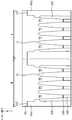
본 발명의 기술적 사상에 의한 다른 양태에 따른 집적회로 소자는 기판의 제1 영역에서 돌출되어 일직선상에 배치되고 제1 도전형의 제1 채널 영역을 가지는 한 쌍의 제1 핀형 활성 영역과, 상기 한 쌍의 제1 핀형 활성 영역의 하부에서 상기 한 쌍의 제1 핀형 활성 영역의 양 측벽을 덮는 저레벨 제1 소자분리막과, 상기 한 쌍의 제1 핀형 활성 영역의 사이를 가로지르는 고레벨 제1 소자분리막과, 상기 제1 영역을 한정하기 위하여 상기 기판 내부로 상기 제1 저레벨 소자분리막보다 더 깊은 레벨까지 연장되고, 상기 저레벨 제1 소자분리막의 일부와 접해 있는 제1 소자영역간 분리용 절연막과, 상기 저레벨 제1 소자분리막, 상기 고레벨 제1 소자분리막, 및 상기 제1 소자영역간 분리용 절연막 중 상기 저레벨 제1 소자분리막 내에만 형성되고, 상기 제1 채널 영역에 제1 응력을 인가하도록 상기 한 쌍의 제1 핀형 활성 영역의 양 측벽을 따라 연장된 제1 스트레서 라이너를 포함한다.According to another aspect of the present invention, there is provided an integrated circuit device comprising: a pair of first pinned active regions which are arranged in a straight line and protrude from a first region of a substrate and have a first channel region of a first conductivity type; A first low-level first isolation film covering both side walls of the pair of first pin-type active regions at a lower portion of the pair of first pin-type active regions; A first element region isolation insulating film extending to a level deeper than the first low-level element isolation film into the substrate to define the first region and being in contact with a part of the low-level first element isolation film; Level insulating film is formed only in the low-level first element isolation film among the low-level first element isolation film, the high-level first element isolation film, and the first element region separation insulating film, To include a first seuteureseo liner extending along the side walls of the first pin-shaped active regions of the pair to apply a first stress.
일부 실시예들에서, 상기 한 쌍의 제1 핀형 활성 영역 중 적어도 하나의 제1 핀형 활성 영역은 상기 제1 영역에 형성된 제1 트렌치에 의해 한정되고, 상기 저레벨 제1 소자분리막은 상기 제1 트렌치 내에서 상기 적어도 하나의 제1 핀형 활성 영역에 접하는 제1 절연 라이너와, 상기 제1 절연 라이너 위에서 상기 적어도 하나의 제1 핀형 활성 영역의 측벽을 따라 연장되는 상기 제1 스트레서 라이너와, 상기 제1 스트레서 라이너 위에서 상기 제1 트렌치를 채우는 제1 매립 절연막을 포함할 수 있다.In some embodiments, at least one first pinned active region of the pair of first pinned active regions is defined by a first trench formed in the first region, and the low- A first insulating liner in contact with the at least one first pinned active region within the at least one first pinned active region; a first insulating liner in contact with the at least one first pinned active region within the first insulating liner; And a first buried insulating film filling the first trench on the stressor liner.
일부 실시예들에서, 상기 고레벨 제1 소자분리막은 상기 한 쌍의 제1 핀형 활성 영역의 사이에 있는 제1 핀 분리 영역에 형성되고, 상기 고레벨 제1 소자분리막은 상기 제1 핀 분리 영역 내에서 상기 한 쌍의 제1 핀형 활성 영역에 접하고 상기 제1 핀 분리 영역을 채우는 핀 분리 절연막으로 이루어질 수 있다.In some embodiments, the high-level first element isolation film is formed in a first fin-type isolation region between the pair of first fin-shaped active regions, and the high-level first element isolation film is formed in the first fin- And a pin separation insulating film contacting the first pinned active region and filling the first fin separation region.
일부 실시예들에서, 상기 저레벨 제1 소자분리막은 상기 한 쌍의 제1 핀형 활성 영역의 상면보다 더 낮은 레벨의 상면을 가지고, 상기 고레벨 제1 소자분리막은 상기 한 쌍의 제1 핀형 활성 영역의 상면보다 더 높은 레벨의 상면을 가질 수 있다.In some embodiments, the low-level first isolation layer has a lower level top surface than the top surface of the pair of first pinned active areas, and the high-level first isolation layer has a top surface of the pair of first pinned active areas It may have a higher level of the upper surface than the upper surface.
본 발명의 기술적 사상에 의한 다른 양태에 따른 집적회로 소자는 상기 한 쌍의 제1 핀형 활성 영역 위에서 상기 한 쌍의 제1 핀형 활성 영역의 연장 방향에 교차하는 방향으로 연장되는 적어도 하나의 제1 노말 게이트와, 상기 고레벨 제1 소자분리막 위에서 상기 적어도 하나의 제1 노말 게이트와 평행하게 연장되는 제1 더미 게이트를 더 포함할 수 있다.The integrated circuit device according to another aspect of the technical idea of the present invention includes at least one first normally active region extending in a direction crossing the extending direction of the pair of first pinned active regions on the pair of first pinned active regions Gate and a first dummy gate extending on the high-level first device isolation film in parallel with the at least one first normal gate.
본 발명의 기술적 사상에 의한 다른 양태에 따른 집적회로 소자는 상기 한 쌍의 제1 핀형 활성 영역 위에서 상기 한 쌍의 제1 핀형 활성 영역의 연장 방향에 교차하는 방향으로 연장되는 적어도 하나의 제1 노말 게이트와, 상기 고레벨 제1 소자분리막 위에서 상기 적어도 하나의 제1 노말 게이트와 평행하게 연장되는 절연 라인을 더 포함할 수 있다.The integrated circuit device according to another aspect of the technical idea of the present invention includes at least one first normally active region extending in a direction crossing the extending direction of the pair of first pinned active regions on the pair of first pinned active regions Gate and an isolation line extending parallel to the at least one first normal gate on the high-level first isolation film.
본 발명의 기술적 사상에 의한 다른 양태에 따른 집적회로 소자는 상기 한 쌍의 제1 핀형 활성 영역 위에서 상기 한 쌍의 제1 핀형 활성 영역의 연장 방향에 교차하는 방향으로 연장되는 적어도 하나의 제1 노말 게이트를 포함하고, 상기 고레벨 제1 소자분리막은 상기 한 쌍의 제1 핀형 활성 영역의 사이에 있는 제1 핀 분리 영역을 채우면서 상기 적어도 하나의 제1 노말 게이트와 동일 레벨에서 상기 적어도 하나의 제1 노말 게이트와 평행하게 연장되는 핀 분리 절연막을 포함할 수 있다.The integrated circuit device according to another aspect of the technical idea of the present invention includes at least one first normally active region extending in a direction crossing the extending direction of the pair of first pinned active regions on the pair of first pinned active regions Wherein the high-level first isolation film is formed by filling the first fin-type isolation region between the pair of first pin-type active regions and forming the at least one first N- And a pin separation insulating film extending in parallel with the first normal gate.
본 발명의 기술적 사상에 의한 다른 양태에 따른 집적회로 소자에서, 상기 저레벨 제1 소자분리막에서, 상기 제1 스트레서 라이너와 상기 저레벨 제1 소자분리막의 저면과의 사이의 수직 최단 거리는 상기 제1 스트레서 라이너와 상기 저레벨 제1 소자분리막의 측벽과의 수평 최단 거리보다 더 클 수 있다.In the integrated circuit device according to another aspect of the technical idea of the present invention, in the low-level first element isolation film, the vertical shortest distance between the first stressor liner and the bottom surface of the low- Level first element isolation film and the side wall of the low-level first element isolation film.
일부 실시예들에서, 상기 제1 스트레서 라이너는 상기 제1 소자영역간 분리용 절연막과 접할 수 있다. 다른 일부 실시예들에서, 상기 제1 스트레서 라이너는 상기 제1 소자영역간 분리용 절연막으로부터 이격될 수 있다.In some embodiments, the first stressor liner may be in contact with the insulating film for isolation between the first element regions. In some other embodiments, the first stressor liner may be spaced from the first insulating film for isolation between element regions.
본 발명의 기술적 사상에 의한 다른 양태에 따른 집적회로 소자에서, 상기 제1 스트레서 라이너는 제1 산화물 라이너를 사이에 두고 상기 한 쌍의 제1 핀형 활성 영역으로부터 이격될 수 있다. 그리고, 상기 제1 산화물 라이너는 상기 저레벨 제1 소자분리막의 측벽을 제공하는 제1 부분과 상기 저레벨 제1 소자분리막의 저면을 제공하는 제2 부분을 포함하고, 상기 제1 부분의 두께보다 상기 제2 부분의 두께가 더 클 수 있다.In an integrated circuit device according to another aspect of the present inventive concept, the first stressor liner may be spaced from the pair of first pinned active areas across a first oxide liner. The first oxide liner includes a first portion providing a sidewall of the low-level first element isolation film and a second portion providing a bottom surface of the low-level first element isolation film, wherein the thickness of the first portion is greater than the thickness of the first portion. The thickness of the two portions may be larger.
본 발명의 기술적 사상에 의한 다른 양태에 따른 집적회로 소자는 상기 기판의 제2 영역에서 돌출되어 일직선상에 배치되고 제2 도전형의 제2 채널 영역을 가지는 한 쌍의 제2 핀형 활성 영역과, 상기 한 쌍의 제2 핀형 활성 영역의 하부에서 상기 한 쌍의 제2 핀형 활성 영역의 양 측벽을 덮는 저레벨 제2 소자분리막과, 상기 한 쌍의 제2 핀형 활성 영역의 사이를 가로지르는 고레벨 제2 소자분리막과, 상기 제2 영역을 한정하기 위하여 상기 기판 내부로 상기 제2 저레벨 소자분리막보다 더 깊은 레벨까지 연장되고, 상기 저레벨 제2 소자분리막의 일부와 접해 있는 제2 소자영역간 분리용 절연막과, 상기 저레벨 제2 소자분리막, 상기 고레벨 제2 소자분리막, 및 상기 제2 소자영역간 분리용 절연막 중 상기 저레벨 제2 소자분리막 내에만 형성되고, 상기 제2 채널 영역에 상기 제1 응력과 다른 제2 응력을 인가하도록 상기 한 쌍의 제2 핀형 활성 영역의 양 측벽을 따라 연장된 제2 스트레서 라이너를 더 포함할 수 있다.According to another aspect of the present invention, there is provided an integrated circuit device comprising: a pair of second pinned active regions protruding from a second region of the substrate and disposed in a straight line and having a second channel region of a second conductivity type; And a low-level second isolation film covering both side walls of the pair of second pin-type active regions at a lower portion of the pair of second pin-type active regions; A second element isolation insulating film which extends to a level deeper than the second low level element isolation film into the substrate to define the second region and is in contact with a part of the low level second element isolation film; Level insulating film is formed only in the low-level second element isolation film among the low-level second element isolation film, the high-level second element isolation film, and the second element region isolation insulating film, In a region wherein the may further comprise a second seuteureseo liner extending along the side walls of the second pin-shaped active regions of the pair to apply a first stress and a second, different stress.
일부 실시예들에서, 상기 제1 스트레서 라이너 및 상기 제2 스트레서 라이너는 서로 동일한 물질로 이루어지고, 서로 다른 두께를 가질 수 있다.In some embodiments, the first and second stressor liners are made of the same material and may have different thicknesses.
일부 실시예들에서, 상기 제2 스트레서 라이너는 제2 산화물 라이너를 사이에 두고 상기 한 쌍의 제2 핀형 활성 영역으로부터 이격되어 있다. 그리고, 상기 제2 산화물 라이너는 상기 저레벨 제2 소자분리막의 측벽을 제공하는 제1 부분과 상기 저레벨 제1 소자분리막의 저면을 제공하는 제2 부분을 포함하고, 상기 제1 부분의 두께보다 상기 제2 부분의 두께가 더 클 수 있다.In some embodiments, the second stressor liner is spaced from the pair of second pinned active areas across a second oxide liner. The second oxide liner includes a first portion that provides a sidewall of the low-level second isolation film and a second portion that provides a bottom of the low-level first isolation film, wherein the thickness of the first portion is greater than the thickness of the first portion. The thickness of the two portions may be larger.
본 발명의 기술적 사상에 의한 또 다른 양태에 따른 집적회로 소자는 기판의 제1 영역에 형성된 제1 핀형 활성 영역과, 상기 기판의 제2 영역에 형성된 제2 핀형 활성 영역과, 상기 제1 핀형 활성 영역의 단축 방향의 양 측벽을 덮는 제1 소자분리막과, 상기 제1 핀형 활성 영역의 장축 방향의 양 측벽을 덮는 제1 핀 분리 절연막과, 상기 제2 핀형 활성 영역의 단축 방향의 양 측벽을 덮는 제2 소자분리막과, 상기 제2 핀형 활성 영역의 장축 방향의 양 측벽을 덮는 제2 핀 분리 절연막과, 상기 제1 영역과 상기 제2 영역과의 사이에 형성된 소자영역간 분리용 절연막과, 상기 제1 소자분리막, 상기 제1 핀 분리 절연막, 및 상기 소자영역간 분리용 절연막 중 상기 제1 소자분리막 내에만 형성된 제1 스트레서 라이너와, 상기 제2 소자분리막, 상기 제2 핀 분리 절연막, 및 상기 소자영역간 분리용 절연막 중 상기 제2 소자분리막 내에만 형성된 제2 스트레서 라이너를 포함한다.According to another aspect of the present invention, an integrated circuit device includes a first pinned active region formed in a first region of a substrate, a second pinned active region formed in a second region of the substrate, A first pin separation insulating film which covers both longitudinally opposite side walls of the first pinned active region and a second pin separation insulating film which covers both short side walls in the minor axis direction of the second pinned active region; A second pin separation insulating film covering the both side walls in the major axis direction of the second pin type active region; an insulating film for isolation between element regions formed between the first region and the second region; A first finer separation insulating film, a first finer separation insulating film, and a second finer separation insulating film formed only in the first element isolation film among the first element isolation film, the first fin separation insulating film, For the inter-region of the element isolation insulating film and a second seuteureseo liner formed only in the second element-isolating film.
본 발명의 기술적 사상에 의한 또 다른 양태에 따른 집적회로 소자에서, 상기 제1 스트레서 라이너 및 상기 제2 스트레서 라이너 중 적어도 하나는 상기 소자영역간 분리용 절연막과 접할 수 있다.In the integrated circuit device according to another aspect of the technical idea of the present invention, at least one of the first and second stressor liners may be in contact with the insulating film for isolation between the element regions.
본 발명의 기술적 사상에 의한 또 다른 양태에 따른 집적회로 소자에서, 상기 제1 스트레서 라이너 및 상기 제2 스트레서 라이너 중 적어도 하나는 상기 소자영역간 분리용 절연막으로부터 이격될 수 있다.In the integrated circuit device according to another aspect of the technical idea of the present invention, at least one of the first and second stressor liner and the second stressor liner may be spaced apart from the insulating film for isolation between the element regions.
본 발명의 기술적 사상에 의한 또 다른 양태에 따른 집적회로 소자에서, 상기 제1 스트레서 라이너는 상기 제1 핀형 활성 영역에 제1 응력을 인가하도록 상기 제1 핀형 활성 영역의 단축 방향의 양 측벽을 따라 연장될 수 있다. 그리고, 상기 제2 스트레서 라이너는 상기 제2 핀형 활성 영역에 상기 제1 응력과 다른 제2 응력을 인가하도록 상기 제2 핀형 활성 영역의 단축 방향의 양 측벽을 따라 연장될 수 있다.In an integrated circuit device according to another aspect of the technical aspect of the present invention, the first stressor liner is disposed along both short side walls of the first pinned active area to apply a first stress to the first pinned active area Can be extended. The second stressor liner may extend along both short side walls of the second pinned active region to apply a second stress different from the first stress to the second pinned active region.
본 발명의 기술적 사상에 의한 또 다른 양태에 따른 집적회로 소자에서, 상기 제1 스트레서 라이너의 두께와 상기 제2 스트레서 라이너의 두께는 서로 다를 수 있다.In the integrated circuit device according to another aspect of the technical idea of the present invention, the thickness of the first and second stressor liners may be different from each other.
본 발명의 기술적 사상에 의한 또 다른 양태에 따른 집적회로 소자에서, 상기 제1 소자분리막은 상기 제1 핀형 활성 영역의 상면보다 더 낮은 레벨의 상면을 가질 수 있다. 그리고, 상기 제1 핀 분리 절연막은 상기 제1 핀형 활성 영역의 상면과 같거나 더 높은 레벨의 상면을 가지고, 상기 제2 소자분리막은 상기 제2 핀형 활성 영역의 상면보다 더 낮은 레벨의 상면을 가지고, 상기 제2 핀 분리 절연막은 상기 제2 핀형 활성 영역의 상면과 같거나 더 높은 레벨의 상면을 가질 수 있다.In the integrated circuit device according to another aspect of the technical idea of the present invention, the first isolation film may have a lower level upper surface than the upper surface of the first fin-shaped active region. The first pin-isolation insulating film has a top surface that is equal to or higher than the top surface of the first fin-shaped active region, and the second device isolation film has a top surface having a lower level than the top surface of the second fin- , The second fin-type isolation layer may have a top surface of the same level as or higher than the top surface of the second pinned active area.
본 발명의 기술적 사상에 의한 집적회로 소자는 서로 다른 도전형의 채널 영역을 포함하는 제1 영역 및 제2 영역에서 서로 다른 적층 구조를 가지는 소자분리막을 포함한다. 또한, 도전형이 서로 다른 채널 영역들을 가지는 서로 다른 영역에서, 소자분리막 중 필요한 영역에 선택적으로 서로 다른 응력을 가지는 스트레서(stressor) 라이너를 형성함으로써 채널 영역들마다 캐리어 이동도를 독립적으로 향상시킬 수 있다.The integrated circuit device according to the technical idea of the present invention includes a device isolation film having different lamination structures in a first region and a second region including channel regions of different conductivity types. Further, in a different region having different channel regions of the conductive type, a stressor liner selectively having different stresses is formed in a necessary region of the element isolation film, thereby independently improving the carrier mobility for each channel region have.
도 1a는 본 발명의 기술적 사상에 의한 실시예들에 따른 집적회로 소자의 주요 구성을 도시한 평면 레이아웃 다이어그램이다.
도 1b는 도 1a의 X1 - X1' 선 및 X2 - X2' 선 단면도이다.
도 1c는 본 발명의 기술적 사상에 의한 다른 실시예에 따른 집적회로 소자의 단면도이다.
도 2는 본 발명의 기술적 사상에 의한 또 다른 실시예에 따른 집적회로 소자의 단면도이다.
도 3은 본 발명의 기술적 사상에 의한 또 다른 실시예에 따른 집적회로 소자의 단면도이다.
도 4a는 본 발명의 기술적 사상에 의한 또 다른 실시예에 따른 집적회로 소자의 단면도이고, 도 4b는 도 4a에 예시한 복수의 제1 핀형 활성 영역을 확대하여 도시한 단면도이고, 도 4c는 도 4a에 예시한 복수의 제2 핀형 활성 영역을 확대하여 도시한 단면도이다.
도 4d는 본 발명의 기술적 사상에 의한 또 다른 실시예에 따른 집적회로 소자의 단면도이다.
도 5는 본 발명의 기술적 사상에 의한 또 다른 실시예에 따른 집적회로 소자의 단면도이다.
도 6은 본 발명의 기술적 사상에 의한 또 다른 실시예에 따른 집적회로 소자의 단면도이다.
도 7은 본 발명의 기술적 사상에 의한 또 다른 실시예에 따른 집적회로 소자의 단면도이다.
도 8a는 본 발명의 기술적 사상에 의한 또 다른 실시예에 따른 집적회로 소자의 단면도이다.
도 8b는 본 발명의 기술적 사상에 의한 또 다른 실시예에 따른 집적회로 소자의 단면도이다.
도 9는 본 발명의 기술적 사상에 의한 또 다른 실시예에 따른 집적회로 소자의 단면도이다.
도 10은 본 발명의 기술적 사상에 의한 또 다른 실시예에 따른 집적회로 소자의 단면도이다.
도 11a 내지 도 11e는 본 발명의 기술적 사상에 의한 다른 실시예들에 따른 집적회로 소자를 도시한 도면들로서, 도 11a는 집적회로 소자의 주요 구성을 도시한 평면 레이아웃 다이어그램이고, 도 11b는 도 11a의 B - B' 선 단면도이고, 도 11c는 도 11a의 C - C' 선 단면도이고, 도 11d는 도 11a의 D - D' 선 단면도이고, 도 11e는 도 11a의 E - E' 선 단면도이다.
도 12a 및 도 12b는 본 발명의 기술적 사상에 의한 또 다른 실시예들에 따른 집적회로 소자의 단면도들이다.
도 13a 및 도 13b는 본 발명의 기술적 사상에 의한 또 다른 실시예들에 따른 집적회로 소자의 단면도들이다.
도 14는 본 발명의 기술적 사상에 의한 다른 실시예들에 따른 집적회로 소자의 평면 레이아웃 다이어그램이다.
도 15a 및 도 15b는 본 발명의 기술적 사상에 의한 또 다른 실시예들에 따른 집적회로 소자의 단면도들이다.
도 16a 및 도 16b는 본 발명의 기술적 사상에 의한 또 다른 실시예들에 따른 집적회로 소자의 단면도들이다.
도 17a 내지 도 17c는 본 발명의 기술적 사상에 의한 다른 실시예들에 따른 집적회로 소자를 도시한 도면들로서, 도 17a는 집적회로 소자의 평면 레이아웃 다이어그램이고, 도 17b는 도 17a의 B - B' 선 단면도이고, 도 17c는 도 17a의 C - C' 선 단면도이다.
도 18a 내지 도 18j는 본 발명의 기술적 사상에 의한 실시예들에 따른 집적회로 소자의 제조 방법을 설명하기 위하여 공정 순서에 따라 도시한 단면도들이다.
도 19a 내지 도 19c는 본 발명의 기술적 사상에 의한 다른 실시예에 따른 집적회로 소자의 제조 방법을 설명하기 위한 단면도들이다.
도 20은 본 발명의 기술적 사상에 의한 실시예들에 따른 전자 소자의 블록 다이어그램이다.
도 21은 본 발명의 기술적 사상에 의한 메모리 모듈의 평면도이다.
도 22는 본 발명의 기술적 사상에 의한 실시예들에 따른 디스플레이 구동 집적회로 (display driver IC: DDI) 및 상기 DDI를 구비하는 디스플레이 장치의 개략적인 블록 다이어그램이다.
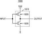
도 23은 본 발명의 기술적 사상에 의한 실시예들에 따른 CMOS 인버터의 회로도이다.
도 24는 본 발명의 기술적 사상에 의한 실시예들에 따른 CMOS SRAM 소자의 회로도이다.
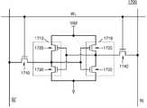
도 25는 본 발명의 기술적 사상에 의한 실시예들에 따른 CMOS NAND 회로의 회로도이다.
도 26은 본 발명의 기술적 사상에 의한 실시예들에 따른 전자 시스템을 도시한 블록 다이어그램이다.
도 27은 본 발명의 기술적 사상에 의한 실시예들에 따른 전자 시스템의 블록 다이어그램이다.BRIEF DESCRIPTION OF DRAWINGS FIG. 1A is a plan layout diagram showing a main configuration of an integrated circuit device according to embodiments of the present invention; FIG.
1B is a cross-sectional view taken along line X1-X1 'and X2-X2' in FIG. 1A.
1C is a cross-sectional view of an integrated circuit device according to another embodiment of the present invention.
2 is a cross-sectional view of an integrated circuit device according to another embodiment of the present invention.
3 is a cross-sectional view of an integrated circuit device according to another embodiment of the present invention.
FIG. 4A is a cross-sectional view of an integrated circuit device according to another embodiment of the present invention, FIG. 4B is an enlarged cross-sectional view of a plurality of first pinned active regions illustrated in FIG. 4A, 4A is an enlarged cross-sectional view of a plurality of second pin-shaped active regions.
4D is a cross-sectional view of an integrated circuit device according to still another embodiment of the present invention.
5 is a cross-sectional view of an integrated circuit device according to another embodiment of the present invention.
6 is a cross-sectional view of an integrated circuit device according to another embodiment of the present invention.
7 is a cross-sectional view of an integrated circuit device according to another embodiment of the present invention.
8A is a cross-sectional view of an integrated circuit device according to still another embodiment of the present invention.
8B is a cross-sectional view of an integrated circuit device according to another embodiment of the present invention.
9 is a cross-sectional view of an integrated circuit device according to still another embodiment of the present invention.
10 is a cross-sectional view of an integrated circuit device according to still another embodiment of the present invention.
FIGS. 11A to 11E are diagrams showing integrated circuit elements according to other embodiments according to technical aspects of the present invention, wherein FIG. 11A is a plan layout diagram showing a main configuration of an integrated circuit element, FIG. 11A is a cross-sectional view taken along the line C-C 'of FIG. 11A, FIG. 11D is a sectional view taken along line D-D' of FIG. 11A, and FIG. 11E is a sectional view taken along the line E-E ' .
12A and 12B are cross-sectional views of an integrated circuit device according to still another embodiment of the present invention.
13A and 13B are cross-sectional views of an integrated circuit device according to still another embodiment of the present invention.
14 is a plan layout diagram of an integrated circuit device according to another embodiment of the present invention.
15A and 15B are cross-sectional views of an integrated circuit device according to still another embodiment of the present invention.
16A and 16B are cross-sectional views of an integrated circuit device according to still another embodiment of the present invention.
17A is a plan layout diagram of an integrated circuit device, and FIG. 17B is a cross-sectional view taken along the line B-B 'in FIG. 17A. FIG. 17A is a plan view of the integrated circuit device according to another embodiment of the present invention. And Fig. 17C is a sectional view taken along the line C-C 'in Fig. 17A.
18A to 18J are cross-sectional views illustrating a method of fabricating an integrated circuit device according to embodiments of the present invention.
19A to 19C are cross-sectional views illustrating a method of manufacturing an integrated circuit device according to another embodiment of the present invention.
20 is a block diagram of an electronic device according to embodiments of the present invention.
21 is a plan view of a memory module according to the technical idea of the present invention.
FIG. 22 is a schematic block diagram of a display driver IC (DDI) according to embodiments of the present invention and a display device including the DDI.
23 is a circuit diagram of a CMOS inverter according to embodiments of the present invention.
24 is a circuit diagram of a CMOS SRAM device according to embodiments of the present invention.
25 is a circuit diagram of a CMOS NAND circuit according to embodiments of the present invention.
26 is a block diagram illustrating an electronic system according to embodiments of the present invention.
27 is a block diagram of an electronic system according to embodiments of the present invention.
이하, 첨부 도면을 참조하여 본 발명의 실시예들을 상세히 설명한다. 도면상의 동일한 구성요소에 대해서는 동일한 참조부호를 사용하고, 이들에 대한 중복된 설명은 생략한다.Hereinafter, embodiments of the present invention will be described in detail with reference to the accompanying drawings. The same reference numerals are used for the same constituent elements in the drawings, and a duplicate description thereof will be omitted.
본 발명의 실시예들은 당해 기술 분야에서 통상의 지식을 가진 자에게 본 발명을 더욱 완전하게 설명하기 위하여 제공되는 것으로, 아래의 실시예들은 여러 가지 다른 형태로 변형될 수 있으며, 본 발명의 범위가 아래의 실시예들로 한정되는 것은 아니다. 오히려, 이들 실시예는 본 개시를 더욱 충실하고 완전하게 하며 당업자에게 본 발명의 사상을 완전하게 전달하기 위하여 제공되는 것이다.Embodiments of the present invention will now be described more fully hereinafter with reference to the accompanying drawings, in which exemplary embodiments of the invention are shown. These embodiments are provided so that this disclosure will be thorough and complete, and will fully convey the scope of the invention to those skilled in the art. The present invention is not limited to the following embodiments. Rather, these embodiments are provided so that this disclosure will be more thorough and complete, and will fully convey the concept of the invention to those skilled in the art.
본 명세서에서 제1, 제2 등의 용어가 다양한 부재, 영역, 층들, 부위 및/또는 구성 요소들을 설명하기 위하여 사용되지만, 이들 부재, 부품, 영역, 층들, 부위 및/또는 구성 요소들은 이들 용어에 의해 한정되어서는 안 됨은 자명하다. 이들 용어는 특정 순서나 상하, 또는 우열을 의미하지 않으며, 하나의 부재, 영역, 부위, 또는 구성 요소를 다른 부재, 영역, 부위 또는 구성 요소와 구별하기 위하여만 사용된다. 따라서, 이하 상술할 제1 부재, 영역, 부위 또는 구성 요소는 본 발명의 가르침으로부터 벗어나지 않고서도 제2 부재, 영역, 부위 또는 구성 요소를 지칭할 수 있다. 예를 들어, 본 발명의 권리 범위로부터 이탈되지 않은 채 제1 구성 요소는 제2 구성 요소로 명명될 수 있고, 유사하게 제2 구성 요소도 제1 구성 요소로 명명될 수 있다.Although the terms first, second, etc. are used herein to describe various elements, regions, layers, regions and / or elements, these elements, components, regions, layers, regions and / It should not be limited by. These terms do not imply any particular order, top, bottom, or top row, and are used only to distinguish one member, region, region, or element from another member, region, region, or element. Thus, a first member, region, region, or element described below may refer to a second member, region, region, or element without departing from the teachings of the present invention. For example, without departing from the scope of the present invention, the first component may be referred to as a second component, and similarly, the second component may also be referred to as a first component.
달리 정의되지 않는 한, 여기에 사용되는 모든 용어들은 기술 용어와 과학 용어를 포함하여 본 발명 개념이 속하는 기술 분야에서 통상의 지식을 가진 자가 공통적으로 이해하고 있는 바와 동일한 의미를 지닌다. 또한, 통상적으로 사용되는, 사전에 정의된 바와 같은 용어들은 관련되는 기술의 맥락에서 이들이 의미하는 바와 일관되는 의미를 갖는 것으로 해석되어야 하며, 여기에 명시적으로 정의하지 않는 한 과도하게 형식적인 의미로 해석되어서는 아니 될 것임은 이해될 것이다.Unless otherwise defined, all terms used herein have the same meaning as commonly understood by one of ordinary skill in the art to which the inventive concept belongs, including technical terms and scientific terms. In addition, commonly used, predefined terms are to be interpreted as having a meaning consistent with what they mean in the context of the relevant art, and unless otherwise expressly defined, have an overly formal meaning It will be understood that it will not be interpreted.
어떤 실시예가 달리 구현 가능한 경우에 특정한 공정 순서는 설명되는 순서와 다르게 수행될 수도 있다. 예를 들어, 연속하여 설명되는 두 공정이 실질적으로 동시에 수행될 수도 있고, 설명되는 순서와 반대의 순서로 수행될 수도 있다.If certain embodiments are otherwise feasible, the particular process sequence may be performed differently from the sequence described. For example, two processes that are described in succession may be performed substantially concurrently, or may be performed in the reverse order to that described.
첨부 도면에 있어서, 예를 들면, 제조 기술 및/또는 공차에 따라, 도시된 형상의 변형들이 예상될 수 있다. 따라서, 본 발명의 실시예들은 본 명세서에 도시된 영역의 특정 형상에 제한된 것으로 해석되어서는 아니 되며, 예를 들면 제조 과정에서 초래되는 형상의 변화를 포함하여야 한다. 여기에 사용되는 모든 용어 "및/또는"은 언급된 구성 요소들의 각각 및 하나 이상의 모든 조합을 포함한다. 또한, 본 명세서에서 사용되는 용어 "기판"은 기판 그 자체, 또는 기판과 그 표면에 형성된 소정의 층 또는 막 등을 포함하는 적층 구조체를 의미할 수 있다. 또한, 본 명세서에서 "기판의 표면"이라 함은 기판 그 자체의 노출 표면, 또는 기판 위에 형성된 소정의 층 또는 막 등의 외측 표면을 의미할 수 있다.In the accompanying drawings, for example, variations in the shape shown may be expected, depending on manufacturing techniques and / or tolerances. Accordingly, embodiments of the present invention should not be construed as limited to any particular shape of the regions shown herein, but should include variations in shape resulting from, for example, manufacturing processes. All terms "and / or" as used herein encompass each and every one or more combinations of the recited elements. In addition, the term "substrate" as used herein can mean a substrate itself, or a laminated structure including a substrate and a predetermined layer or film formed on the surface thereof. Further, in the present specification, the term "surface of a substrate" may mean an exposed surface of the substrate itself, or an outer surface such as a predetermined layer or a film formed on the substrate.
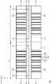
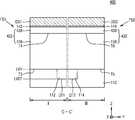
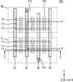
도 1a는 본 발명의 기술적 사상에 의한 실시예들에 따른 집적회로 소자(100)의 주요 구성을 도시한 평면 레이아웃 다이어그램이다.FIG. 1A is a planar layout diagram showing a main configuration of an
도 1b는 도 1a의 X1 - X1' 선 및 X2 - X2' 선 단면도이다.1B is a cross-sectional view taken along line X1-X1 'and X2-X2' in FIG. 1A.
도 1a 및 도 1b를 참조하면, 집적회로 소자(100)는 제1 영역(I) 및 제2 영역(II)을 가지는 기판(110)을 포함한다.1A and 1B, an
상기 기판(110)은 Si 또는 Ge와 같은 반도체, 또는 SiGe, SiC, GaAs, InAs, 또는 InP와 같은 화합물 반도체를 포함할 수 있다. 일부 실시예들에서, 상기 기판(110)은 III-V 족 물질 및 IV 족 물질 중 적어도 하나로 이루어질 수 있다. 상기 III-V 족 물질은 적어도 하나의 III 족 원소와 적어도 하나의 V족 원소를 포함하는 2 원계, 3 원계, 또는 4 원계 화합물일 수 있다. 상기 III-V 족 물질은 III 족 원소로서 In, Ga 및 Al 중 적어도 하나의 원소와, V 족 원소로서 As, P 및 Sb 중 적어도 하나의 원소를 포함하는 화합물일 수 있다. 예를 들면, 상기 III-V 족 물질은 InP, InzGa1-zAs (0 ≤ z ≤ 1), 및 AlzGa1-zAs (0 ≤ z ≤ 1)로부터 선택될 수 있다. 상기 2 원계 화합물은, 예를 들면 InP, GaAs, InAs, InSb 및 GaSb 중 어느 하나일 수 있다. 상기 3 원계 화합물은 InGaP, InGaAs, AlInAs, InGaSb, GaAsSb 및 GaAsP 중 어느 하나일 수 있다. 상기 IV 족 물질은 Si 또는 Ge일 수 있다. 그러나, 본 발명의 기술적 사상에 의한 집적회로 소자에서 사용 가능한 III-V 족 물질 및 IV 족 물질이 상기 예시한 바에 한정되는 것은 아니다. 상기 III-V 족 물질과 Ge과 같은 IV 족 물질은 저전력, 고속 트랜지스터를 만들 수 있는 채널 재료로 이용될 수 있다. Si 기판에 비해 전자의 이동도가 높은 III-V 족 물질, 예를 들면 GaAs로 이루어지는 반도체 기판과, Si 기판에 비해 정공의 이동도가 높은 반도체 물질, 예를 들면 Ge로 이루어지는 반도체 기판을 이용하여 고성능 CMOS를 형성할 수 있다. 일부 실시예들에서, 상기 기판(110) 상에 MMOS 트랜지스터를 형성하는 경우, 상기 기판(110)은 위에서 예시한 III-V 족 물질들 중 어느 하나로 이루어질 수 있다. 다른 일부 실시예들에서, 상기 기판(110) 상에 PMOS 트랜지스터를 형성하는 경우, 상기 기판(110)은 Ge로 이루어질 수 있다. 다른 예에서, 상기 기판(110)은 SOI (silicon on insulator) 구조를 가질 수 있다. 상기 기판(110)은 도전 영역, 예를 들면 불순물이 도핑된 웰 (well), 또는 불순물이 도핑된 구조물을 포함할 수 있다.The
상기 기판(110)의 제1 영역(I) 및 제2 영역(II)은 상기 기판(110)의 서로 다른 영역들을 지칭하는 것으로, 서로 다른 문턱 전압이 요구되는 영역들일 수 있다. 예를 들면, 상기 제1 영역(I)은 NMOS 영역이고, 상기 제2 영역(II)은 PMOS 영역일 수 있다.The first region I and the second region II of the
상기 기판(110)의 제1 영역(I)으로부터 상기 기판(110)의 주면에 수직인 방향 (Z 방향)으로 복수의 제1 핀형 활성 영역(F1)이 돌출되어 있다. 상기 복수의 제1 핀형 활성 영역(F1)은 제1 도전형 채널 영역(CH1)을 가질 수 있다. 상기 복수의 제1 핀형 활성 영역(F1)은 각각 상기 제1 도전형 채널 영역(CH1)의 하부에서 양 측벽이 복수의 제1 소자분리막(120)으로 덮여 있다.A plurality of first pinned active regions F1 protrude from a first region I of the
상기 기판(110)의 제2 영역(II)으로부터 상기 기판(110)의 주면에 수직인 방향 (Z 방향)으로 복수의 제2 핀형 활성 영역(F2)이 돌출되어 있다. 상기 복수의 제2 핀형 활성 영역(F2)은 제2 도전형 채널 영역(CH2)을 가질 수 있다. 상기 복수의 제2 핀형 활성 영역(F2)은 각각 상기 제2 도전형 채널 영역(CH2)의 하부에서 양 측벽이 복수의 제2 소자분리막(130)으로 덮여 있다.A plurality of second pinned active regions F2 protrude from the second region II of the
도 1a 및 도 1b에는 제1 영역(I)에 4 개의 제1 핀형 활성 영역(F1)이 형성되고 제2 영역(II)에 4 개의 제2 핀형 활성 영역(F2)이 형성된 경우를 예시하였으나, 본 발명의 기술적 사상은 이에 한정되지 않는다. 예를 들면, 제1 영역(I) 및 제2 영역(II)에서 각각 1 개 내지 3 개, 또는 5 개 이상의 핀형 활성 영역이 형성될 수도 있다. 또한, 도 1b에는 상기 복수의 제1 핀형 활성 영역(F1) 및 복수의 제2 핀형 활성 영역(F2)이 각각 기판(110)의 주면에 수직인 방향 (Z 방향)으로 연장되는 중심선을 기준으로 그 양 측벽의 프로파일이 대략 대칭 형상을 가지도록 형성된 경우를 예시하였다. 그러나, 본 발명의 기술적 사상은 예시한 바에 한정되지 않으며, 다양한 형상을 가지는 복수의 제1 핀형 활성 영역(F1) 및 복수의 제2 핀형 활성 영역(F2)을 포함할 수 있다.Although FIGS. 1A and 1B illustrate the case where four first pin-type active regions F1 are formed in the first region I and four second pin-type active regions F2 are formed in the second region II, The technical idea of the present invention is not limited thereto. For example, one to three or five or more pinned active regions may be formed in the first region I and the second region II, respectively. 1B, the plurality of first pinned active regions F1 and the plurality of second pinned active regions F2 are formed on the basis of a center line extending in a direction (Z direction) perpendicular to the main surface of the
상기 제1 소자분리막(120)과 상기 제2 소자분리막(130)은 서로 다른 적층 구조를 가진다.The first
상기 제1 소자분리막(120)은 상기 제1 핀형 활성 영역(F1)을 한정하는 제1 트렌치(T1)의 적어도 일부를 채우도록 형성될 수 있다. 상기 제1 소자분리막(120)은 상기 제1 트렌치(T1)의 내벽으로부터 차례로 적층된 제1 절연 라이너(122), 제1 스트레서 라이너 (stressor liner)(124), 및 제1 매립 절연막(126)을 포함할 수 있다. 상기 제1 절연 라이너(122)는 상기 제1 핀형 활성 영역(F1)의 측벽에 접하도록 형성될 수 있다. 상기 제1 스트레서 라이너(124)는 상기 제1 절연 라이너(122)를 사이에 두고 상기 제1 핀형 활성 영역(F1)의 양 측벽을 따라 연장되도록 형성될 수 있다. 상기 제1 매립 절연막(126)은 상기 제1 스트레서 라이너(124) 위에서 상기 제1 트렌치(T1) 내부를 채울 수 있다.The
상기 제1 절연 라이너(122)는 제1 산화막으로 이루어질 수 있다. 예를 들면, 상기 제1 절연 라이너(122)는 자연산화막으로 이루어질 수 있다. 일부 실시예들에서, 상기 제1 절연 라이너(122)를 구성하는 제1 산화막은 상기 제1 핀형 활성 영역(F1)의 표면을 열산화시키는 공정을 수행하여 얻어질 수 있다. 일부 실시예들에서, 상기 제1 절연 라이너(122)는 약 10 ∼ 100 Å의 두께를 가질 수 있다.The first insulating
상기 제1 스트레서 라이너(124)는 상기 제1 도전형 채널 영역(CH1)에 제1 응력을 인가하는 물질로 형성될 수 있다. 상기 제1 스트레서 라이너(124)는 상기 제1 핀형 활성 영역(F1)의 제1 도전형 채널 영역(CH1)에 제1 응력을 도입함으로써 상기 제1 도전형 채널 영역(CH1)에서의 캐리어 이동도를 개선하는 역할을 할 수 있다. 일부 실시예들에서, 상기 제1 도전형 채널 영역(CH1)이 N 형 채널 영역인 경우 상기 제1 스트레서 라이너(124)는 상기 제1 도전형 채널 영역(CH1)에 인장 응력을 인가하는 물질로 이루어질 수 있다. 예를 들면, 상기 제1 스트레서 라이너(124)는 SiN (silicon nitride), SiON (silicon oxynitride), SiBN (silicon boronitride), SiC (silicon carbide), SiC:H, SiCN, SiCN:H, SiOCN, SiOCN:H, SiOC (silicon oxycarbide), SiO2 (silicon dioxide), 폴리실리콘, 또는 이들의 조합으로 이루어질 수 있다. 일부 실시예들에서, 상기 제1 스트레서 라이너(124)는 약 10 ∼ 100 Å의 두께를 가질 수 있다.The
상기 제1 매립 절연막(126)은 제2 산화막으로 이루어질 수 있다. 상기 제1 산화막 및 상기 제2 산화막은 서로 다른 방법으로 얻어지는 산화막일 수 있다. 일부 실시예들에서, 상기 제1 매립 절연막(126)을 구성하는 제2 산화막은 증착 공정 또는 코팅 공정에 의해 형성된 막으로 이루어질 수 있다. 일부 실시예들에서, 상기 제1 매립 절연막(126)은 FCVD (flowable chemical vapor deposition) 공정 또는 스핀 코팅 (spin coating) 공정에 의해 형성된 산화막으로 이루어질 수 있다. 예를 들면, 상기 제1 매립 절연막(126)은 FSG (fluoride silicate glass), USG (undoped silicate glass), BPSG (boro-phospho-silicate glass), PSG (phospho-silicate glass), FOX (flowable oxide), PE-TEOS (plasma enhanced tetra-ethyl-ortho-silicate), 또는 TOSZ (tonen silazene)로 이루어질 수 있으나, 이들에 한정되는 것은 아니다.The first buried insulating
상기 복수의 제2 소자분리막(130)은 상기 제2 핀형 활성 영역(F2)을 한정하는 제2 트렌치(T2)의 적어도 일부를 채우도록 형성될 수 있다. 상기 복수의 제2 소자분리막(130)은 상기 제2 트렌치(T2)의 내벽으로부터 차례로 적층된 제2 절연 라이너(132), 제2 스트레서 라이너(134), 및 제2 매립 절연막(136)을 포함할 수 있다.The plurality of
상기 제2 절연 라이너(132)는 상기 제2 핀형 활성 영역(F2)의 측벽에 접하도록 형성될 수 있다. 상기 제2 스트레서 라이너(134)는 상기 제2 절연 라이너(132)를 사이에 두고 상기 제2 핀형 활성 영역(F2)의 측벽을 덮도록 형성될 수 있다. 상기 제2 매립 절연막(136)은 상기 제2 절연 라이너(132) 및 상기 제2 스트레서 라이너(134)를 사이에 두고 상기 제2 핀형 활성 영역(F2)의 측벽을 덮도록 형성될 수 있다.The second
상기 제2 절연 라이너(132)는 제3 산화막으로 이루어질 수 있다. 예를 들면, 상기 제2 절연 라이너(132)는 자연산화막으로 이루어질 수 있다. 상기 제2 절연 라이너(132)는 상기 제2 핀형 활성 영역(F2)의 표면을 산화시키는 공정을 수행하여 얻어질 수 있다. 예를 들면, 상기 제2 절연 라이너(132)는 열 산화 공정을 이용하여 형성된 산화막으로 이루어질 수 있다. 일부 실시예들에서, 상기 제2 절연 라이너(132)를 구성하는 상기 제3 산화막은 상기 제1 절연 라이너(122)를 구성하는 제1 산화막과 동일한 공정에 의해 형성된 동일한 물질막으로 이루어질 수 있다. 일부 실시예들에서, 상기 제2 절연 라이너(132)는 약 10 ∼ 100 Å의 두께를 가질 수 있다.The second
상기 제2 스트레서 라이너(134)는 상기 제2 도전형 채널 영역(CH2)에 상기 제1 응력과 다른 제2 응력을 인가하는 물질로 형성될 수 있다. 상기 제2 스트레서 라이너(134)는 상기 제2 핀형 활성 영역(F2)의 제2 도전형 채널 영역(CH2)에 제2 응력을 도입함으로써 상기 제2 도전형 채널 영역(CH2)에서의 캐리어 이동도를 개선하는 역할을 할 수 있다. 일부 실시예들에서, 상기 제2 도전형 채널 영역(CH2)이 P 형 채널 영역인 경우 상기 제2 스트레서 라이너(134)는 상기 제2 도전형 채널 영역(CH2)에 압축 응력을 인가하는 물질로 이루어질 수 있다. 예를 들면, 상기 제2 스트레서 라이너(134)는 SiN, SiON, SiBN, SiC, SiC:H, SiCN, SiCN:H, SiOCN, SiOCN:H, SiOC, SiO2, 폴리실리콘, 또는 이들의 조합으로 이루어질 수 있다. 일부 실시예들에서, 상기 제2 스트레서 라이너(134)는 상기 제1 스트레서 라이너(124)와 동일 물질로 이루어지되, 인접해 있는 채널 영역에 서로 다른 응력을 인가하는 물질로 구성될 수 있다. 상기 제1 스트레서 라이너(124) 및 제2 스트레서 라이너(134)는 서로 동일한 두께를 가질 수도 있고 서로 다른 두께를 가질 수도 있다. 상기 제1 스트레서 라이너(124) 및 제2 스트레서 라이너(134)는 각각 서로 다른 공정을 통해 형성된 막으로 이루어질 수 있다. 일부 실시예들에서, 상기 제2 스트레서 라이너(134)는 약 10 ∼ 100 Å의 두께를 가질 수 있다.The
상기 제2 매립 절연막(136)은 제4 산화막으로 이루어질 수 있다. 상기 제2 매립 절연막(136)은 증착 공정 또는 코팅 공정에 의해 형성된 막으로 이루어질 수 있다. 일부 실시예들에서, 상기 제2 매립 절연막(136)은 FCVD 공정 또는 스핀 코팅 공정에 의해 형성된 산화막으로 이루어질 수 있다. 예를 들면, 상기 제2 매립 절연막(136)은 FSG, USG, BPSG, PSG, FOX, PE-TEOS, 또는 TOSZ로 이루어질 수 있다. 일부 실시예들에서, 상기 제2 매립 절연막(136)을 구성하는 제4 산화막은 상기 제1 매립 절연막(126)을 구성하는 제2 산화막과 동일한 공정에 의해 형성된 동일한 물질막으로 이루어질 수 있다.The second buried insulating
상기 기판(110)의 제1 영역(I) 상에서 상기 복수의 제1 핀형 활성 영역(F1) 및 상기 제1 소자분리막(120) 위에는 상기 복수의 제1 핀형 활성 영역(F1) 각각의 양 측벽 및 상면을 덮는 제1 게이트 절연막(142) 및 제1 게이트(152)가 형성되어 있다. 상기 제1 게이트 절연막(142) 및 상기 제1 게이트(152)는 상기 복수의 제1 핀형 활성 영역(F1)의 연장 방향 (X 방향)에 교차하는 방향 (Y 방향)으로 연장될 수 있다.The first pinned active region F1 and the first
상기 기판(110)의 제1 영역(I) 및 제2 영역(II)에는 제1 트렌치(T1) 및 제2 트렌치(T2) 각각의 깊이보다 더 큰 깊이를 가지는 제1 딥 트렌치(DT1) 및 제2 딥 트렌치(DT2)가 형성될 수 있다. 일부 실시예들에서, 상기 제1 딥 트렌치(DT1) 및 제2 딥 트렌치(DT2)는 상기 제1 영역(I) 및 상기 제2 영역(II) 각각의 에지 영역, 또는 상기 제1 영역(I)과 상기 제2 영역(II)과의 사이의 영역에 형성될 수 있다.A first deep trench DT1 having a depth greater than the depth of each of the first trench T1 and the second trench T2 is formed in the first region I and the second region II of the
상기 제1 딥 트렌치(DT1)의 내부는 제1 소자영역간 분리용 절연막(112)으로 채워질 수 있다. 상기 제2 딥 트렌치(DT2) 내부는 제2 소자영역간 분리용 절연막(114)으로 채워질 수 있다.The inside of the first deep trench DT1 may be filled with the first inter-element
상기 제1 소자영역간 분리용 절연막(112)은 제1 영역(I)을 한정하기 위하여 기판(110) 내부로 상기 복수의 제1 소자분리막(120)보다 더 깊은 레벨까지 연장될 수 있다. 상기 제1 소자영역간 분리용 절연막(112)은 복수의 제1 소자분리막(120)의 일부와 접해 있을 수 있다.The first inter-element
상기 제2 소자영역간 분리용 절연막(114)은 제2 영역(II)을 한정하기 위하여 기판(110) 내부로 상기 복수의 제2 소자분리막(130)보다 더 깊은 레벨까지 연장될 수 있다. 상기 제2 소자영역간 분리용 절연막(114)은 복수의 제2 소자분리막(130)의 일부와 접해 있을 수 있다.The second inter-element-
또한, 도 1b에 예시한 바와 같이, 제1 영역(I)에서 상기 제1 스트레서 라이너(124)는 상기 제1 소자영역간 분리용 절연막(112)과 직접 접할 수 있다. 그리고, 제2 영역(II)에서 상기 제2 스트레서 라이너(134)는 상기 제2 소자영역간 분리용 절연막(114)과 직접 접할 수 있다.1B, in the first region I, the
상기 제1 소자영역간 분리용 절연막(112) 및 제2 소자영역간 분리용 절연막(114)은 제5 산화막으로 이루어질 수 있다. 일부 실시예들에서, 상기 제5 산화막은 코팅 공정 또는 증착 공정에 의해 형성된 막으로서, 상기 제1 및 제2 소자분리막(120, 130)을 구성하는 제1 및 제2 매립 절연막(126, 136)과는 다른 물질로 이루어질 수 있다. 예를 들면, 상기 제1 및 제2 매립 절연막(126, 136)을 구성하는 제2 및 제4 산화막은 각각 FSG로 이루어지고, 상기 소자영역간 분리용 절연막(112)을 구성하는 제5 산화막은 USG로 이루어질 수 있다.The first inter-element-region
상기 기판(110)의 제2 영역(II) 상에서 상기 복수의 제2 핀형 활성 영역(F2) 및 상기 복수의 제2 소자분리막(130) 위에는 상기 복수의 제2 핀형 활성 영역(F2) 각각의 양 측벽 및 상면을 덮는 제2 게이트 절연막(144) 및 제2 게이트(154)가 형성되어 있다. 상기 제2 게이트 절연막(144) 및 상기 제2 게이트(154)는 상기 복수의 제2 핀형 활성 영역(F2)의 연장 방향 (X 방향)에 교차하는 방향 (Y 방향)으로 연장될 수 있다.On the second region (II) of the substrate (110), on the plurality of second pinned active regions (F2) and the plurality of second isolation films (130), the amount of each of the plurality of second pinned active regions A second
상기 제1 및 제2 게이트 절연막(142, 144)은 각각 상기 제1 및 게2 게이트(152, 154)의 저면 및 양 측벽을 덮도록 형성될 수 있다.The first and second
상기 제1 및 제2 게이트 절연막(142, 144)은 각각 실리콘 산화막, 고유전막, 또는 이들의 조합으로 이루어질 수 있다. 상기 고유전막은 실리콘 산화막보다 유전 상수가 더 큰 물질로 이루어질 수 있다. 예를 들면, 상기 제1 및 제2 게이트 절연막(142, 144)은 약 10 내지 25의 유전 상수를 가질 수 있다. 상기 고유전막은 하프늄 산화물 (hafnium oxide), 하프늄 산질화물 (hafnium oxynitride), 하프늄 실리콘 산화물 (hafnium silicon oxide), 란타늄 산화물 (lanthanum oxide), 란타늄 알루미늄 산화물 (lanthanum aluminum oxide), 지르코늄 산화물 (zirconium oxide), 지르코늄 실리콘 산화물 (zirconium silicon oxide), 탄탈륨 산화물 (tantalum oxide), 티타늄 산화물 (titanium oxide), 바륨 스트론튬 티타늄 산화물 (barium strontium titanium oxide), 바륨 티타늄 산화물 (barium titanium oxide), 스트론튬 티타늄 산화물 (strontium titanium oxide), 이트륨 산화물 (yttrium oxide), 알루미늄 산화물 (aluminum oxide), 납 스칸듐 탄탈륨 산화물 (lead scandium tantalum oxide), 및 납 아연 니오브산염 (lead zinc niobate), 및 이들의 조합 중에서 선택되는 물질로 이루어질 수 있으나, 상기 고유전막을 구성하는 물질이 상기 예시된 바에 한정되는 것은 아니다. 상기 제1 및 제2 게이트 절연막(142, 144)은 ALD (atomic layer deposition), CVD (chemical vapor deposition), 또는 PVD (physical vapor deposition) 공정에 의해 형성될 수 있다. 일부 실시예들에서, 상기 제1 게이트 절연막(142) 및 제2 게이트 절연막(144)은 서로 동일한 구조를 가질 수 있다. 다른 일부 실시예들에서, 상기 제1 게이트 절연막(142) 및 제2 게이트 절연막(144)은 서로 다른 구조를 가질 수 있다.The first and second
상기 제1 및 제2 게이트(152, 154)는 각각 일함수 조절용 금속 함유층과, 상기 일함수 조절용 금속 함유층의 상부에 형성된 공간을 채우는 갭필용 금속 함유층을 포함할 수 있다. 일부 실시예들에서, 상기 제1 및 제2 게이트(152, 154)는 각각 금속 질화물층, 금속층, 도전성 캡핑층, 및 갭필 (gap-fill) 금속막이 차례로 적층된 구조를 가질 수 있다. 상기 금속 질화물층 및 금속층은 각각 Ti, W, Ru, Nb, Mo, Hf, Ni, Co, Pt, Yb, Tb, Dy, Er, 및 Pd 중에서 선택되는 적어도 하나의 금속을 포함할 수 있다. 상기 금속 질화물층 및 금속층은 각각 ALD, MOALD (metal organic ALD), 또는 MOCVD (metal organic CVD) 공정에 의해 형성될 수 있다. 상기 도전성 캡핑층은 상기 금속층의 표면이 산화되는 것을 방지하는 보호막 역할을 할 수 있다. 또한, 상기 도전성 캡핑층은 상기 금속층 위에 다른 도전층이 증착될 때 증착을 용이하게 하기 위한 접착층 (wetting layer) 역할을 할 수 있다. 상기 도전성 캡핑층은 금속 질화물, 예를 들면 TiN, TaN, 또는 이들의 조합으로 이루어질 수 있으나, 이에 한정되는 것은 아니다. 상기 갭필 금속막은 상기 도전성 캡핑층 위에 연장될 수 있다. 상기 갭필 금속막은 W 막으로 이루어질 수 있다. 상기 갭필 금속막은 ALD, CVD, 또는 PVD 공정에 의해 형성될 수 있다. 상기 갭필 금속막은 상기 도전성 캡핑층의 상면에서의 단차부에 의해 형성되는 리세스 공간을 보이드 (void) 없이 매립할 수 있다. 일부 실시예들에서, 상기 제1 게이트(152) 및 상기 제2 게이트(154)는 서로 다른 구성을 가질 수 있다.The first and
상기 기판(110)의 제1 영역(I) 상에서, 상기 제1 핀형 활성 영역(F1) 중 상기 제1 게이트(152)의 양 측에는 제1 소스/드레인 영역(162)이 형성되어 있다. 상기 기판(110)의 제2 영역(II) 상에서, 상기 제2 핀형 활성 영역(F2) 중 상기 제2 게이트(154)의 양 측에는 제2 소스/드레인 영역(164)이 형성되어 있다.On the first region I of the
도시하지는 않았으나, 상기 제1 및 제2 소스/드레인 영역(162, 164)은 각각 상기 제1 및 제2 핀형 활성 영역(F1, F2)으로부터 에피텍셜 성장된 반도체층을 포함할 수 있다. 상기 제1 및 제2 소스/드레인 영역(162, 164)은 각각 에피텍셜 성장된 복수의 SiGe층을 포함하는 임베디드 SiGe 구조, 에피텍셜 성장된 Si 층, 또는 에피텍셜 성장된 SiC 층으로 이루어질 수 있다. 상기 제1 소스/드레인 영역(162) 및 상기 제2 소스/드레인 영역(164)은 서로 다른 구성을 가질 수 있다.Although not shown, the first and second source /
도 1c는 본 발명의 기술적 사상에 의한 다른 실시예에 따른 집적회로 소자(100A)의 단면도로서, 도 1a의 X1 - X1' 선 및 X2 - X2' 선 단면에 대응하는 단면도이다. 도 1c에 있어서, 도 1a 및 도 1b에서와 동일한 참조 부호는 동일 부재를 나타내며, 여기서는 이들에 대한 상세한 설명은 생략한다.FIG. 1C is a cross-sectional view of an
도 1c에 예시한 집적회로 소자(100A)는 제1 영역(I)에서 복수의 제1 핀형 활성 영역(F1)의 제1 도전형 채널 영역(CH1)과 제1 게이트 절연막(142)과의 사이에 제1 인터페이스막(interfacial layer)(IF1)이 개재되어 있고, 제2 영역(II)에서 복수의 제2 핀형 활성 영역(F2)의 제2 도전형 채널 영역(CH2)과 제2 게이트 절연막(144)과의 사이에 제2 인터페이스막(IF2)이 개재되어 있는 것을 제외하고 도 1b에 예시한 집적회로 소자(100)와 대체로 동일한 구성을 가진다.The
일부 실시예들에서, 상기 제1 인터페이스막(IF1) 및 제2 인터페이스막(IF2)은 각각 복수의 제1 핀형 활성 영역(F1) 및 복수의 제2 핀형 활성 영역(F2)의 표면을 산화시켜 얻어질 수 있다.In some embodiments, the first interface film IF1 and the second interface film IF2 oxidize the surfaces of the plurality of first pinned active areas F1 and the plurality of second pinned active areas F2, respectively, Can be obtained.
상기 제1 인터페이스막(IF1)은 복수의 제1 핀형 활성 영역(F1)에 접해 있고, 상기 제2 인터페이스막(IF2)은 복수의 제2 핀형 활성 영역(F2)에 접해 있을 수 있다. 상기 제1 인터페이스막(IF1)은 복수의 제1 핀형 활성 영역(F1)과 제1 게이트 절연막(142)과의 사이의 계면 결함을 치유하는 역할을 할 수 있다. 상기 제2 인터페이스막(IF2)은 복수의 제2 핀형 활성 영역(F2)과 제2 게이트 절연막(144)과의 사이의 계면 결함을 치유하는 역할을 할 수 있다.The first interface film IF1 may be in contact with the plurality of first pinned active areas F1 and the second interface film IF2 may be in contact with the plurality of second pinned active areas F2. The first interface film IF1 may serve to heal an interface defect between the first pinned active region F1 and the first
일부 실시예들에서, 상기 제1 인터페이스막(IF1) 및 제2 인터페이스막(IF2)은 유전율이 약 9 이하인 저유전 물질층, 예를 들면 실리콘 산화막, 실리콘 산질화막, 또는 이들의 조합으로 이루어질 수 있다. 다른 일부 실시예들에서, 상기 제1 인터페이스막(IF1) 및 제2 인터페이스막(IF2)은 실리케이트, 실리케이트와 실리콘 산화막과의 조합, 또는 실리케이트와 실리콘 산질화막과의 조합으로 이루어질 수 있다.In some embodiments, the first interface film IF1 and the second interface film IF2 may be made of a low dielectric material layer having a dielectric constant of about 9 or less, for example, a silicon oxide film, a silicon oxynitride film, or a combination thereof have. In some other embodiments, the first interface film IF1 and the second interface film IF2 may be formed of a combination of a silicate, a silicate and a silicon oxide film, or a combination of a silicate and a silicon oxynitride film.
일부 실시예들에서, 상기 제1 인터페이스막(IF1) 및 제2 인터페이스막(IF2)은 각각 약 5 ∼ 20 Å의 두께를 가질 수 있으나, 이에 한정되는 것은 아니다.In some embodiments, the first interface film IF1 and the second interface film IF2 may each have a thickness of about 5 to 20 angstroms, but are not limited thereto.
도 1a 내지 도 1c를 참조하여 설명한 집적회로 소자(100, 100A)에서, 제1 영역(I)에 형성된 복수의 제1 소자분리막(120)에는 제1 핀형 활성 영역(F1)의 제1 도전형 채널 영역(CH1)에 제1 응력을 인가하도록 상기 제1 핀형 활성 영역(F1)의 양 측벽을 따라 연장된 제1 스트레서 라이너(124)가 포함되어 있고, 제2 영역(II)에 형성된 복수의 제2 소자분리막(130)에는 제2 핀형 활성 영역(F2)의 제2 도전형 채널 영역(CH2)에 상기 제1 응력과 다른 제2 응력을 인가하도록 상기 제2 핀형 활성 영역(F2)의 양 측벽을 따라 연장된 제2 스트레서 라이너(134)가 포함되어 있다. 이에 따라, 상기 제1 핀형 활성 영역(F1)의 제1 도전형 채널 영역(CH1) 및 제2 핀형 활성 영역(F2)의 제2 도전형 채널 영역(CH2)에서 각각의 캐리어 이동도를 독립적으로 향상시킬 수 있는 응력이 인가됨으로써, 제1 영역(I) 및 제2 영역(II)에 형성되는 트랜지스터들의 퍼포먼스가 향상될 수 있다.In the
도 2는 본 발명의 기술적 사상에 의한 다른 실시예에 따른 집적회로 소자(100B)의 단면도로서, 도 1a의 X1 - X1' 선 및 X2 - X2' 선 단면에 대응하는 단면도이다. 도 2에 있어서, 도 1a 및 도 1b에서와 동일한 참조 부호는 동일 부재를 나타내며, 여기서는 이들에 대한 상세한 설명은 생략한다.FIG. 2 is a cross-sectional view of an
도 2를 참조하면, 제1 영역(I)에서 복수의 제1 핀형 활성 영역(F1)은 각각 제1 도전형 채널 영역(CH1)의 하부에서 양 측벽이 복수의 제1 소자분리막(120A)으로 덮여 있다. 제2 영역(II)에서 복수의 제2 핀형 활성 영역(F2)은 각각 제2 도전형 채널 영역(CH2)의 하부에서 양 측벽이 복수의 제2 소자분리막(130A)으로 덮여 있다.Referring to FIG. 2, in the first region I, a plurality of first pinned active regions F1 are formed in the lower portion of the first conductive type channel region CH1 such that both side walls are divided into a plurality of first
상기 복수의 제1 소자분리막(120A)은 제1 트렌치(T1)의 내벽으로부터 차례로 적층된 제1 절연 라이너(122), 제1 스트레서 라이너(124A), 및 제1 매립 절연막(126)을 포함할 수 있다.The plurality of first
상기 복수의 제2 소자분리막(130A)은 제2 트렌치(T2)의 내벽으로부터 차례로 적층된 제2 절연 라이너(132), 제2 스트레서 라이너(134A), 및 제2 매립 절연막(136)을 포함할 수 있다.The plurality of
상기 제1 소자분리막(120A)에 포함된 제1 스트레서 라이너(124A)의 두께는 상기 제2 소자분리막(130A)에 포함된 제2 스트레서 라이너(134A)의 두께보다 더 작을 수 있다. 예를 들면, 상기 제1 스트레서 라이너(124A)는 약 10 ∼ 40 Å의 두께를 가지고, 상기 제2 스트레서 라이너(134A)는 약 50 ∼ 100 Å의 두께를 가질 수 있으나, 상기 제1 스트레서 라이너(124A) 및 제2 스트레서 라이너(134A)의 두께가 상기 예시한 바에 한정되는 것은 아니다.The thickness of the
일부 실시예들에서, 상기 제1 스트레서 라이너(124A)와 상기 제2 스트레서 라이너(134A)는 서로 동일한 물질로 이루어질 수 있다. 다른 일부 실시예들에서, 상기 제1 스트레서 라이너(124A)와 상기 제2 스트레서 라이너(134A)는 서로 다른 물질로 이루어질 수 있다. 상기 제1 스트레서 라이너(124A) 및 제2 스트레서 라이너(134A)에 대한 보다 상세한 사항은 도 1a 및 도 1b를 참조하여 제1 스트레서 라이너(124) 및 제2 스트레서 라이너(134)에 대하여 설명한 바와 대체로 동일하다.In some embodiments, the first and
도 2에는 도시하지 않았으나, 도 1c에 예시한 집적회로 소자(100A)와 유사하게, 집적회로 소자(100B)는 제1 영역(I)에서 복수의 제1 핀형 활성 영역(F1)과 제1 게이트 절연막(142)과의 사이에 개재된 제1 인터페이스막(IF1)과, 제2 영역(II)에서 복수의 제2 핀형 활성 영역(F2)과 제2 게이트 절연막(144)과의 사이에 개재된 제2 인터페이스막(IF2)을 더 포함할 수 있다.Similar to the
도 3은 본 발명의 기술적 사상에 의한 또 다른 실시예에 따른 집적회로 소자(100C)의 단면도로서, 도 1a의 X1 - X1' 선 및 X2 - X2' 선 단면에 대응하는 단면도이다. 도 3에 있어서, 도 1a 및 도 1b에서와 동일한 참조 부호는 동일 부재를 나타내며, 여기서는 이들에 대한 상세한 설명은 생략한다.FIG. 3 is a cross-sectional view of an
도 3을 참조하면, 제1 영역(I)에서 복수의 제1 핀형 활성 영역(F1)은 각각 제1 도전형 채널 영역(CH1)의 하부에서 양 측벽이 복수의 제1 소자분리막(120B)으로 덮여 있다. 제2 영역(II)에서 복수의 제2 핀형 활성 영역(F2)은 각각 제2 도전형 채널 영역(CH2)의 하부에서 양 측벽이 복수의 제2 소자분리막(130B)으로 덮여 있다.Referring to FIG. 3, in the first region I, a plurality of first pinned active regions F1 are formed in the lower part of the first conductive type channel region CH1, and both side walls are divided into a plurality of first element isolation films 120B It is covered. In the second region II, the plurality of second pinned active regions F2 are covered with the plurality of
상기 복수의 제1 소자분리막(120B)은 제1 트렌치(T1)의 내벽으로부터 차례로 적층된 제1 절연 라이너(122), 제1 스트레서 라이너(124B), 및 제1 매립 절연막(126)을 포함할 수 있다.The plurality of first element isolation films 120B includes a first insulating
상기 복수의 제2 소자분리막(130B)은 제2 트렌치(T2)의 내벽으로부터 차례로 적층된 제2 절연 라이너(132), 제2 스트레서 라이너(134B), 및 제2 매립 절연막(136)을 포함할 수 있다.The plurality of
상기 제1 소자분리막(120B)에 포함된 제1 스트레서 라이너(124B)의 두께는 상기 제2 소자분리막(130B)에 포함된 제2 스트레서 라이너(134B)의 두께보다 더 클 수 있다. 예를 들면, 상기 제1 스트레서 라이너(124B)는 약 50 ∼ 100 Å의 두께를 가지고, 상기 제2 스트레서 라이너(134B)는 약 10 ∼ 40 Å의 두께를 가질 수 있으나, 상기 제1 스트레서 라이너(124B) 및 제2 스트레서 라이너(134B)의 두께가 상기 예시한 바에 한정되는 것은 아니다.The thickness of the first stressor liner 124B included in the first device isolation film 120B may be greater than the thickness of the
일부 실시예들에서, 상기 제1 스트레서 라이너(124B)와 상기 제2 스트레서 라이너(134B)는 서로 동일한 물질로 이루어질 수 있다. 다른 일부 실시예들에서, 상기 제1 스트레서 라이너(124B)와 상기 제2 스트레서 라이너(134B)는 서로 다른 물질로 이루어질 수 있다. 상기 제1 스트레서 라이너(124B) 및 제2 스트레서 라이너(134B)에 대한 보다 상세한 사항은 도 1a 및 도 1b를 참조하여 제1 스트레서 라이너(124) 및 제2 스트레서 라이너(134)에 대하여 설명한 바와 대체로 동일하다.In some embodiments, the first and
도 3에는 도시하지 않았으나, 도 1c에 예시한 집적회로 소자(100A)와 유사하게, 집적회로 소자(100C)는 제1 영역(I)에서 복수의 제1 핀형 활성 영역(F1)과 제1 게이트 절연막(142)과의 사이에 개재된 제1 인터페이스막(IF1)과, 제2 영역(II)에서 복수의 제2 핀형 활성 영역(F2)과 제2 게이트 절연막(144)과의 사이에 개재된 제2 인터페이스막(IF2)을 더 포함할 수 있다.Similar to the
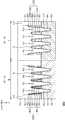
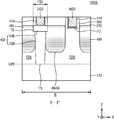
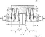
도 4a는 본 발명의 기술적 사상에 의한 또 다른 실시예에 따른 집적회로 소자(200)의 단면도로서, 도 1a의 X1 - X1' 선 및 X2 - X2' 선 단면에 대응하는 단면도이다. 도 4a에 있어서, 도 1a 및 도 1b에서와 동일한 참조 부호는 동일 부재를 나타내며, 여기서는 이들에 대한 상세한 설명은 생략한다.4A is a cross-sectional view of an
도 4a를 참조하면, 제1 영역(I)에는 기판(110)의 주면에 수직인 방향 (Z 방향)으로 복수의 제1 핀형 활성 영역(F1)이 돌출되어 있다. 상기 복수의 제1 핀형 활성 영역(F1)은 상호 평행하게 연장된다.Referring to FIG. 4A, a plurality of first pinned active regions F1 protrude in a direction (Z direction) perpendicular to the main surface of the
상기 복수의 제1 핀형 활성 영역(F1)은 제1 소자영역간 분리용 절연막(112)으로부터 가장 가까운 외측 제1 핀형 활성 영역(F1e)과, 상기 외측 핀형 활성 영역(F1e)을 사이에 두고 제1 소자영역간 분리용 절연막(112)으로부터 이격된 내측 제1 핀형 활성 영역(F1i)을 포함한다.The plurality of first pinned active regions F1 includes an outer first pinned active region F1e closest to the first inter-element
도 4b는 도 4a에 예시한 복수의 제1 핀형 활성 영역(F1)을 확대하여 도시한 단면도이다.4B is an enlarged cross-sectional view of a plurality of first pin-type active regions F1 illustrated in FIG. 4A.
도 4a 및 도 4b를 참조하면, 상기 외측 제1 핀형 활성 영역(F1e)에서, 제1 소자영역간 분리용 절연막(112)에 대면하는 제1 측벽(S1)과 상기 제1 측벽(S1)의 반대측인 제2 측벽(S2)은 기판(110)의 주면에 수직인 방향 (Z 방향)으로 연장되는 중심 축을 기준으로 상호 비대칭 형상을 가진다.4A and 4B, in the outer first pinned active region F1e, a first sidewall S1 facing the first element-to-element
도 4a에 예시한 바와 같이, 제1 영역(I)에서 복수의 제1 소자분리막(220)은 상기 내측 제1 핀형 활성 영역(F1i)의 양 측벽과, 상기 외측 제1 핀형 활성 영역(F1e)의 제2 측벽(S2)을 덮는 내측 제1 소자분리막(220I)과, 상기 외측 제1 핀형 활성 영역(F1e)의 제1 측벽(S1)을 덮는 외측 제1 소자분리막(220E)을 포함한다.4A, in the first region I, a plurality of
상기 복수의 제1 소자분리막(220) 중 상기 제1 측벽(S1)을 덮는 외측 제1 소자분리막(220E)은 상기 제2 측벽(S2)을 덮는 내측 제1 소자분리막(220I)보다 기판(110)의 두께 방향 (Z 방향)으로 더 긴 형상을 가진다.The outer
상기 기판(110)의 두께 방향 (Z 방향)에서, 상기 외측 제1 소자분리막(220E)에 포함된 제1 절연 라이너(222), 제1 스트레서 라이너(224), 및 제1 매립 절연막(226) 각각의 길이는 상기 내측 제1 소자분리막(120I)에 포함된 제1 절연 라이너(122), 제1 스트레서 라이너(124), 및 제1 매립 절연막(126) 각각의 길이보다 더 길다.The first insulating
상기 외측 제1 소자분리막(220E)에 포함된 제1 스트레서 라이너(224)는 상기 제1 소자영역간 분리용 절연막(112)과 접할 수 있다.The
도 4a에 예시한 집적회로 소자(200)의 제2 영역(II)에는 기판(110)의 주면에 수직인 방향 (Z 방향)으로 복수의 제2 핀형 활성 영역(F2)이 돌출되어 있다. 상기 복수의 제2 핀형 활성 영역(F2)은 상호 평행하게 연장된다.A plurality of second pinned active regions F2 protrude in a direction (Z direction) perpendicular to the main surface of the
상기 복수의 제2 핀형 활성 영역(F2)은 제2 소자영역간 분리용 절연막(114)으로부터 가장 가까운 외측 제2 핀형 활성 영역(F2e)과, 상기 외측 핀형 활성 영역(F2e)을 사이에 두고 제2 소자영역간 분리용 절연막(114)으로부터 이격된 내측 제2 핀형 활성 영역(F2i)을 포함한다.The second plurality of pin-type active regions F2 includes an outer second pinned active region F2e closest to the second insulating
도 4c는 도 4a에 예시한 복수의 제2 핀형 활성 영역(F2)을 확대하여 도시한 단면도이다.4C is an enlarged cross-sectional view of a plurality of second pin-type active regions F2 illustrated in FIG. 4A.
도 4a 및 도 4c를 참조하면, 상기 외측 제2 핀형 활성 영역(F2e)에서, 제2 소자영역간 분리용 절연막(114)에 대면하는 제3 측벽(S3)과 상기 제3 측벽(S3)의 반대측인 제4 측벽(S4)은 기판(110)의 주면에 수직인 방향 (Z 방향)으로 연장되는 중심 축을 기준으로 상호 비대칭 형상을 가진다.4A and 4C, in the outer second pin-type active region F2e, a third sidewall S3 facing the
도 4a에 예시한 바와 같이, 제2 영역(II)에서 복수의 제2 소자분리막(230)은 상기 내측 제2 핀형 활성 영역(F2i)의 양 측벽과, 상기 외측 제2 핀형 활성 영역(F2e)의 제4 측벽(S4)을 덮는 내측 제2 소자분리막(230I)과, 상기 외측 제2 핀형 활성 영역(F2e)의 제3 측벽(S3)을 덮는 외측 제2 소자분리막(230E)을 포함한다.4A, in the second region II, a plurality of
상기 복수의 제2 소자분리막(230) 중 상기 제3 측벽(S3)을 덮는 외측 제2 소자분리막(230E)은 상기 제4 측벽(S4)을 덮는 내측 제2 소자분리막(230I)보다 기판(110)의 두께 방향 (Z 방향)으로 더 긴 형상을 가진다.The outer
상기 기판(110)의 두께 방향 (Z 방향)에서, 상기 외측 제2 소자분리막(230E)에 포함된 제2 절연 라이너(232), 제2 스트레서 라이너(234), 및 제2 매립 절연막(236) 각각의 길이는 상기 내측 제2 소자분리막(120I)에 포함된 제2 절연 라이너(132), 제2 스트레서 라이너(134), 및 제2 매립 절연막(136) 각각의 길이보다 더 길다.The second
상기 외측 제2 소자분리막(230E)에 포함된 제2 스트레서 라이너(234)는 상기 제2 소자영역간 분리용 절연막(114)과 접할 수 있다.The
도 4a에 예시한 외측 제1 소자분리막(220E)을 구성하는 제1 절연 라이너(222), 제1 스트레서 라이너(224), 및 제1 매립 절연막(226)에 대한 보다 상세한 사항은 도 1a 및 도 1b를 참조하여 제1 절연 라이너(122), 제1 스트레서 라이너(124), 및 제1 매립 절연막(126)에 대하여 설명한 바와 대체로 동일하다. 또한, 도 4a에 예시한 외측 제2 소자분리막(230E)을 구성하는 제2 절연 라이너(232), 제2 스트레서 라이너(234), 및 제2 매립 절연막(236)에 대한 보다 상세한 사항은 도 1a 및 도 1b를 참조하여 제2 절연 라이너(132), 제2 스트레서 라이너(134), 및 제2 매립 절연막(136)에 대하여 설명한 바와 대체로 동일하다.The details of the first insulating
도 4d는 본 발명의 기술적 사상에 의한 다른 실시예에 따른 집적회로 소자(200A)의 단면도로서, 도 1a의 X1 - X1' 선 및 X2 - X2' 선 단면에 대응하는 단면도이다. 도 4d에 있어서, 도 1a 내지 도 4c에서와 동일한 참조 부호는 동일 부재를 나타내며, 여기서는 이들에 대한 상세한 설명은 생략한다.FIG. 4D is a cross-sectional view of an
도 4d에 예시한 집적회로 소자(200A)는 제1 영역(I)에서 복수의 제1 핀형 활성 영역(F1)의 제1 도전형 채널 영역(CH1)과 제1 게이트 절연막(142)과의 사이에 제1 인터페이스막(IF1)이 개재되어 있고, 제2 영역(II)에서 복수의 제2 핀형 활성 영역(F2)의 제2 도전형 채널 영역(CH2)과 제2 게이트 절연막(144)과의 사이에 제2 인터페이스막(IF2)이 개재되어 있는 것을 제외하고 도 4a에 예시한 집적회로 소자(200)와 대체로 동일한 구성을 가진다.The
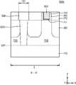
도 5는 본 발명의 기술적 사상에 의한 또 다른 실시예에 따른 집적회로 소자(200B)의 단면도로서, 도 1a의 X1 - X1' 선 및 X2 - X2' 선 단면에 대응하는 단면도이다. 도 5에 있어서, 도 1a, 도 1b, 도 4a 내지 도 4d에서와 동일한 참조 부호는 동일 부재를 나타내며, 여기서는 이들에 대한 상세한 설명은 생략한다.5 is a cross-sectional view of an
도 5를 참조하면, 제1 영역(I)에서 복수의 제1 핀형 활성 영역(F1)은 각각 제1 도전형 채널 영역(CH1)의 하부에서 양 측벽이 복수의 제1 소자분리막(220C)으로 덮여 있다. 상기 복수의 제1 소자분리막(220C)은 도 4a를 참조하여 설명한 바와 유사하게 내측 제1 소자분리막(220I) 및 외측 제1 소자분리막(220E)을 포함한다.5, in the first region I, a plurality of first pinned active regions F1 are formed in the lower portion of the first conductive type channel region CH1, with both side walls being divided into a plurality of first
제2 영역(II)에서 복수의 제2 핀형 활성 영역(F2)은 각각 제2 도전형 채널 영역(CH2)의 하부에서 양 측벽이 복수의 제2 소자분리막(230C)으로 덮여 있다. 상기 복수의 제2 소자분리막(230C)은 도 4a를 참조하여 설명한 바와 유사하게 내측 제2 소자분리막(230I) 및 외측 제2 소자분리막(230E)을 포함한다.In the second region II, the plurality of second pinned active regions F2 are covered with the plurality of
제1 영역(I)에 있는 복수의 제1 소자분리막(220C)에서 내측 제1 소자분리막(220I) 및 외측 제1 소자분리막(220E)을 구성하는 제1 스트레서 라이너(124C, 224C)의 두께는 제2 영역(II)에 있는 복수의 제2 소자분리막(230C)에서 내측 제2 소자분리막(230I) 및 외측 제2 소자분리막(230E)을 구성하는 제2 스트레서 라이너(134C, 234C)의 두께보다 더 작을 수 있다. 예를 들면, 상기 제1 스트레서 라이너(124C, 224C)는 약 10 ∼ 40 Å의 두께를 가지고, 상기 제2 스트레서 라이너(134C, 234C)는 약 50 ∼ 100 Å의 두께를 가질 수 있으나, 상기 제1 스트레서 라이너(124C, 224C) 및 제2 스트레서 라이너(134C, 234C)의 두께가 상기 예시한 바에 한정되는 것은 아니다.The thicknesses of the
일부 실시예들에서, 상기 제1 스트레서 라이너(124C, 224C) 및 제2 스트레서 라이너(134C, 234C)는 서로 동일한 물질로 이루어질 수 있다. 다른 일부 실시예들에서, 상기 제1 스트레서 라이너(124C, 224C) 및 제2 스트레서 라이너(134C, 234C)는 서로 다른 물질로 이루어질 수 있다.In some embodiments, the first and
상기 제1 스트레서 라이너(124C, 224C) 및 제2 스트레서 라이너(134C, 234C)에 대한 보다 상세한 사항은 도 1a 및 도 1b를 참조하여 제1 스트레서 라이너(124) 및 제2 스트레서 라이너(134)에 대하여 설명한 바와 대체로 동일하다.Details of the first and
도 5에는 도시하지 않았으나, 도 4d에 예시한 집적회로 소자(200A)와 유사하게, 집적회로 소자(200B)는 제1 영역(I)에서 복수의 제1 핀형 활성 영역(F1)과 제1 게이트 절연막(142)과의 사이에 개재된 제1 인터페이스막(IF1)과, 제2 영역(II)에서 복수의 제2 핀형 활성 영역(F2)과 제2 게이트 절연막(144)과의 사이에 개재된 제2 인터페이스막(IF2)을 더 포함할 수 있다.Similar to the
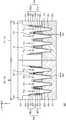
도 6은 본 발명의 기술적 사상에 의한 또 다른 실시예에 따른 집적회로 소자(200C)의 단면도로서, 도 1a의 X1 - X1' 선 및 X2 - X2' 선 단면에 대응하는 단면도이다. 도 6에 있어서, 도 1a 및 도 1b, 도 4a 내지 도 4d에서와 동일한 참조 부호는 동일 부재를 나타내며, 여기서는 이들에 대한 상세한 설명은 생략한다.FIG. 6 is a cross-sectional view of an
도 6을 참조하면, 제1 영역(I)에서 복수의 제1 핀형 활성 영역(F1)은 각각 제1 도전형 채널 영역(CH1)의 하부에서 양 측벽이 복수의 제1 소자분리막(220D)으로 덮여 있다. 상기 복수의 제1 소자분리막(220D)은 도 4a를 참조하여 설명한 바와 유사하게 내측 제1 소자분리막(220I) 및 외측 제1 소자분리막(220E)을 포함한다.Referring to FIG. 6, in the first region I, a plurality of first pinned active regions F1 are formed in the lower portion of the first conductive type channel region CH1, with both side walls being divided into a plurality of first
제2 영역(II)에서 복수의 제2 핀형 활성 영역(F2)은 각각 제2 도전형 채널 영역(CH2)의 하부에서 양 측벽이 복수의 제2 소자분리막(230D)으로 덮여 있다. 상기 복수의 제2 소자분리막(230D)은 도 4a를 참조하여 설명한 바와 유사하게 내측 제2 소자분리막(230I) 및 외측 제2 소자분리막(230E)을 포함한다.In the second region II, the plurality of second pinned active regions F2 are covered with a plurality of
제1 영역(I)에 있는 복수의 제1 소자분리막(220D)에서 내측 제1 소자분리막(220I) 및 외측 제1 소자분리막(220E)을 구성하는 제1 스트레서 라이너(124D, 224D)의 두께는 제2 영역(II)에 있는 복수의 제2 소자분리막(230D)에서 내측 제2 소자분리막(230I) 및 외측 제2 소자분리막(230E)을 구성하는 제2 스트레서 라이너(134D, 234D)의 두께보다 더 작을 수 있다. 예를 들면, 상기 제1 스트레서 라이너(124D, 224D)는 약 10 ∼ 40 Å의 두께를 가지고, 상기 제2 스트레서 라이너(134D, 234D)는 약 50 ∼ 100 Å의 두께를 가질 수 있으나, 상기 제1 스트레서 라이너(124D, 224D) 및 제2 스트레서 라이너(134D, 234D)의 두께가 상기 예시한 바에 한정되는 것은 아니다.The thicknesses of the first and
일부 실시예들에서, 상기 제1 스트레서 라이너(124D, 224D) 및 제2 스트레서 라이너(134D, 234D)는 서로 동일한 물질로 이루어질 수 있다. 다른 일부 실시예들에서, 상기 제1 스트레서 라이너(124D, 224D) 및 제2 스트레서 라이너(134D, 234D)는 서로 다른 물질로 이루어질 수 있다.In some embodiments, the first and
상기 제1 스트레서 라이너(124D, 224D) 및 제2 스트레서 라이너(134D, 234D)에 대한 보다 상세한 사항은 도 1a 및 도 1b를 참조하여 제1 스트레서 라이너(124) 및 제2 스트레서 라이너(134)에 대하여 설명한 바와 대체로 동일하다.Details of the first and
도 6에는 도시하지 않았으나, 도 4d에 예시한 집적회로 소자(200A)와 유사하게, 집적회로 소자(200C)는 제1 영역(I)에서 복수의 제1 핀형 활성 영역(F1)과 제1 게이트 절연막(142)과의 사이에 개재된 제1 인터페이스막(IF1)과, 제2 영역(II)에서 복수의 제2 핀형 활성 영역(F2)과 제2 게이트 절연막(144)과의 사이에 개재된 제2 인터페이스막(IF2)을 더 포함할 수 있다.Like the
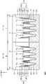
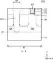
도 7은 본 발명의 기술적 사상에 의한 또 다른 실시예에 따른 집적회로 소자(200D)의 단면도로서, 도 1a의 X1 - X1' 선 및 X2 - X2' 선 단면에 대응하는 단면도이다. 도 7에 있어서, 도 1a 및 도 1b, 도 4a 내지 도 4c에서와 동일한 참조 부호는 동일 부재를 나타내며, 여기서는 이들에 대한 상세한 설명은 생략한다.FIG. 7 is a cross-sectional view of an
도 7을 참조하면, 제1 영역(I)에 있는 복수의 제1 소자분리막(220)에서 외측 제1 소자분리막(220E)을 구성하는 제1 스트레서 라이너(224E)는 제1 소자영역간 분리용 절연막(112)으로부터 이격되어 있다. 그리고, 제2 영역(II)에 있는 복수의 제2 소자분리막(230)에서 외측 제2 소자분리막(230E)을 구성하는 제2 스트레서 라이너(234E)는 제2 소자영역간 분리용 절연막(114)으로부터 이격되어 있다.7, the
상기 외측 제1 소자분리막(220E)을 구성하는 제1 스트레서 라이너(224E)와 상기 외측 제2 소자분리막(230E)을 구성하는 제2 스트레서 라이너(234E)는 각각 내측 제1 소자분리막(220I) 및 내측 제2 소자분리막(230I)에 포함된 제1 스트레서 라이너(124) 및 제2 스트레서 라이너(134)보다 기판(110)의 두께 방향 (Z 방향)에서의 길이가 더 길다.The
도 7에는 도시하지 않았으나, 도 4d에 예시한 집적회로 소자(200A)와 유사하게, 집적회로 소자(200D)는 제1 영역(I)에서 복수의 제1 핀형 활성 영역(F1)과 제1 게이트 절연막(142)과의 사이에 개재된 제1 인터페이스막(IF1)과, 제2 영역(II)에서 복수의 제2 핀형 활성 영역(F2)과 제2 게이트 절연막(144)과의 사이에 개재된 제2 인터페이스막(IF2)을 더 포함할 수 있다.Similar to the
도 8a는 본 발명의 기술적 사상에 의한 또 다른 실시예에 따른 집적회로 소자(300)의 단면도로서, 도 1a의 X1 - X1' 선 및 X2 - X2' 선 단면에 대응하는 단면도이다. 도 8a에 있어서, 도 1a 내지 도 4d에서와 동일한 참조 부호는 동일 부재를 나타내며, 여기서는 이들에 대한 상세한 설명은 생략한다.8A is a cross-sectional view of an
도 8a에 예시한 집적회로 소자(300)는 제1 절연 라이너(122A, 222A) 및 제2 절연 라이너(132A, 232A)의 두께가 위치에 따라 일정하지 않은 것을 제외하고, 도 4a 내지 도 4c에 예시한 집적회로 소자(200)와 대체로 동일한 구성을 가진다.The
도 8a를 참조하면, 제1 영역(I)에서, 복수의 제1 소자분리막(220)에서 내측 제1 소자분리막(220I) 및 외측 제1 소자분리막(220E)을 구성하는 제1 절연 라이너(122A, 222A)는 제1 트렌치(T1)의 측벽에 접하는 부분의 두께보다 저면에 접하는 부분의 두께가 더 크다. 이에 따라, 복수의 제1 소자분리막(220)에서, 제1 스트레서 라이너(124, 224)와 상기 제1 소자분리막(220)의 저면과의 사이의 수직 최단 거리(LV1)는 상기 제1 스트레서 라이너(124, 224)와 상기 제1 소자분리막(220)의 측벽과의 수평 최단 거리(LH1)보다 더 크다.8A, in the first region I, a first insulating
또한, 제2 영역(II)에서, 복수의 제2 소자분리막(230)에서 내측 제2 소자분리막(230I) 및 외측 제2 소자분리막(230E)을 구성하는 제2 절연 라이너(132A, 232A)는 제2 트렌치(T2)의 측벽에 접하는 부분의 두께보다 저면에 접하는 부분의 두께가 더 크다. 이에 따라, 복수의 제2 소자분리막(230)에서, 제2 스트레서 라이너(134, 234)와 상기 제2 소자분리막(230)의 저면과의 사이의 수직 최단 거리(LV2)는 상기 제2 스트레서 라이너(134, 234)와 상기 제2 소자분리막(230)의 측벽과의 수평 최단 거리(LH2)보다 더 크다.In the second region II, the second insulating
상기 제1 절연 라이너(122A, 222A) 및 제2 절연 라이너(132A, 232A)에 대한 보다 상세한 사항은 도 4a 내지 4c를 참조하여 제1 및 제2 절연 라이너(122, 132)에 대하여 설명한 바와 대체로 유사하다.The details of the
제1 영역(I) 및 제2 영역(II)에서, 제1 스트레서 라이너(224)는 제1 소자영역간 분리용 절연막(112)과 접해 있고, 제2 스트레서 라이너(234)는 제2 소자영역간 분리용 절연막(114)과 접해 있다.In the first region I and the second region II, the
도 8b는 본 발명의 기술적 사상에 의한 다른 실시예에 따른 집적회로 소자(300A)의 단면도로서, 도 1a의 X1 - X1' 선 및 X2 - X2' 선 단면에 대응하는 단면도이다. 도 8b에 있어서, 도 1a 내지 도 4d에서와 동일한 참조 부호는 동일 부재를 나타내며, 여기서는 이들에 대한 상세한 설명은 생략한다.FIG. 8B is a cross-sectional view of an
도 8b에 예시한 집적회로 소자(300A)는 제1 영역(I)에서 복수의 제1 핀형 활성 영역(F1)의 제1 도전형 채널 영역(CH1)과 제1 게이트 절연막(142)과의 사이에 제1 인터페이스막(IF1)이 개재되어 있고, 제2 영역(II)에서 복수의 제2 핀형 활성 영역(F2)의 제2 도전형 채널 영역(CH2)과 제2 게이트 절연막(144)과의 사이에 제2 인터페이스막(IF2)이 개재되어 있는 것을 제외하고 도 8a에 예시한 집적회로 소자(300)와 대체로 동일한 구성을 가진다.The
도 9는 본 발명의 기술적 사상에 의한 또 다른 실시예에 따른 집적회로 소자(300B)의 단면도로서, 도 1a의 X1 - X1' 선 및 X2 - X2' 선 단면에 대응하는 단면도이다. 도 9에 있어서, 도 1a 내지 도 8b에서와 동일한 참조 부호는 동일 부재를 나타내며, 여기서는 이들에 대한 상세한 설명은 생략한다.FIG. 9 is a cross-sectional view of an
도 9에 예시한 집적회로 소자(300B)는 제1 영역(I) 및 제2 영역(II)에서 제1 스트레서 라이너(224E)가 제1 소자영역간 분리용 절연막(112)으로부터 이격되어 있고, 제2 스트레서 라이너(234E)가 제2 소자영역간 분리용 절연막(114)으로부터 이격되어 있는 것을 제외하고, 도 8a에 예시한 집적회로 소자(300)와 대체로 동일한 구성을 가진다.In the
도 9에는 도시하지 않았으나, 도 8b에 예시한 집적회로 소자(300A)와 유사하게, 집적회로 소자(300B)는 제1 영역(I)에서 복수의 제1 핀형 활성 영역(F1)과 제1 게이트 절연막(142)과의 사이에 개재된 제1 인터페이스막(IF1)과, 제2 영역(II)에서 복수의 제2 핀형 활성 영역(F2)과 제2 게이트 절연막(144)과의 사이에 개재된 제2 인터페이스막(IF2)을 더 포함할 수 있다.8, the
도 10은 본 발명의 기술적 사상에 의한 또 다른 실시예에 따른 집적회로 소자(300C)의 단면도로서, 도 1a의 X1 - X1' 선 및 X2 - X2' 선 단면에 대응하는 단면도이다. 도 10에 있어서, 도 1a 내지 도 9에서와 동일한 참조 부호는 동일 부재를 나타내며, 여기서는 이들에 대한 상세한 설명은 생략한다.10 is a cross-sectional view of an
도 10에 예시한 집적회로 소자(300C)는 내측 제1 소자분리막(220I)이 서로 분리된 2 개의 제1 스트레서 라이너(324)를 포함하고, 내측 제2 소자분리막(230I)이 서로 분리된 2 개의 제2 스트레서 라이너(334)를 포함하는 것을 제외하고, 도 9에 예시한 집적회로 소자(300B)와 대체로 동일한 구성을 가진다.The
제1 영역(I)에서 복수의 내측 제1 소자분리막(220I)은 각각 서로 분리된 2 개의 제1 스트레서 라이너(324)를 포함한다. 상기 서로 분리된 2 개의 제1 스트레서 라이너(324)는 복수의 제1 핀형 활성 영역(F1) 중 서로 다른 제1 핀형 활성 영역(F1)의 측벽을 덮는다.The plurality of inner first element isolation films 220I in the first region I include two
제2 영역(II)에서 복수의 내측 제2 소자분리막(230I)은 각각 서로 분리된 2 개의 제2 스트레서 라이너(334)를 포함한다. 상기 서로 분리된 2 개의 제2 스트레서 라이너(334)는 복수의 제2 핀형 활성 영역(F2) 중 서로 다른 제2 핀형 활성 영역(F2)의 측벽을 덮는다.In the second region II, the plurality of inner second isolation films 230I each include two
도 10에는 도시하지 않았으나, 도 8b에 예시한 집적회로 소자(300A)와 유사하게, 집적회로 소자(300C)는 제1 영역(I)에서 복수의 제1 핀형 활성 영역(F1)과 제1 게이트 절연막(142)과의 사이에 개재된 제1 인터페이스막(IF1)과, 제2 영역(II)에서 복수의 제2 핀형 활성 영역(F2)과 제2 게이트 절연막(144)과의 사이에 개재된 제2 인터페이스막(IF2)을 더 포함할 수 있다.8, the
도 11a 내지 도 11e는 본 발명의 기술적 사상에 의한 다른 실시예들에 따른 집적회로 소자를 도시한 도면들로서, 도 11a는 집적회로 소자(400)의 주요 구성을 도시한 평면 레이아웃 다이어그램이고, 도 11b는 도 11a의 B - B' 선 단면도이고, 도 11c는 도 11a의 C - C' 선 단면도이고, 도 11d는 도 11a의 D - D' 선 단면도이고, 도 11e는 도 11a의 E - E' 선 단면도이다. 도 11a 내지 도 11e에 있어서, 도 1a 내지 도 10에서와 동일한 참조 부호는 동일 부재를 나타내며, 여기서는 이들에 대한 상세한 설명을 생략한다.11A to 11E are diagrams showing integrated circuit elements according to other embodiments according to the technical idea of the present invention. FIG. 11A is a plan layout diagram showing a main configuration of the
도 11a 내지 도 11e를 참조하면, 집적회로 소자(400)는 제1 영역(I) 및 제2 영역(II)을 가지는 기판(110)을 포함한다.11A-11E, an
상기 기판(110)의 제1 영역(I)으로부터 상기 기판(110)의 주면에 수직인 방향 (Z 방향)으로 복수의 제1 핀형 활성 영역(F1A, F1B)이 돌출되어 있다. 상기 복수의 제1 핀형 활성 영역(F1A, F1B)은 제1 도전형 채널 영역(CHA)을 가질 수 있다. 상기 복수의 제1 핀형 활성 영역(F1A, F1B)은 각각 상기 제1 도전형 채널 영역(CHA)의 하부에서 양 측벽이 저레벨 제1 소자분리막(420)으로 덮여 있다.A plurality of first pinned active regions F1A and F1B protrude from a first region I of the
상기 기판(110)의 제2 영역(II)으로부터 제1 방향 (Z 방향)으로 복수의 제2 핀형 활성 영역(F2A, F2B)이 돌출되어 있다. 상기 복수의 제2 핀형 활성 영역(F2A, F2B)은 제2 도전형 채널 영역(CHB)을 가질 수 있다. 상기 복수의 제2 핀형 활성 영역(F2A, F2B)은 각각 상기 제2 도전형 채널 영역(CHB)의 하부에서 양 측벽이 저레벨 제2 소자분리막(430)으로 덮여 있다.A plurality of second pinned active regions F2A and F2B protrude from a second region II of the
상기 복수의 제1 핀형 활성 영역(F1A, F1B) 및 복수의 제2 핀형 활성 영역(F2A, F2B)은 기판(110) 상에서 X 방향을 따라 상호 평행하게 연장될 수 있다. 상기 복수의 제1 핀형 활성 영역(F1A)과 상기 복수의 제1 핀형 활성 영역(F1B)은 이들의 연장 방향에서 제1 핀 분리 영역(FS1)을 사이에 두고 서로 이격되어 있다. 그리고, 상기 복수의 제2 핀형 활성 영역(F2A)과 상기 복수의 제2 핀형 활성 영역(F2B)은 이들의 연장 방향에서 제2 핀 분리 영역(FS2)을 사이에 두고 서로 이격되어 있다. 일부 실시예들에서, 상기 제1 핀 분리 영역(FS1) 및 제2 핀 분리 영역(FS2)은 상호 연결될 수 있다. 다른 일부 실시예들에서, 상기 제1 핀 분리 영역(FS1) 및 제2 핀 분리 영역(FS2)은 서로 이격될 수 있다.The plurality of first pinned active regions F1A and F1B and the plurality of second pinned active regions F2A and F2B may extend parallel to each other along the X direction on the
도 11a에는 제1 핀형 활성 영역(F1A, F1B) 및 제2 핀형 활성 영역(F2A, F2B)이 각각 4 개씩 형성되어 있는 경우를 예시하였으나, 본 발명의 기술적 사상은 이에 한정되지 않는다. 예를 들면, 제1 영역(I) 및 제2 영역(II)에서 제1 핀형 활성 영역(F1A, F1B) 및 제2 핀형 활성 영역(F2A, F2B)의 개수는 다양하게 선택될 수 있다.11A, four first pin-type active regions F1A and F1B and two second pin-type active regions F2A and F2B are formed, but the technical idea of the present invention is not limited thereto. For example, the number of the first pinned active regions F1A and F1B and the number of the second pinned active regions F2A and F2B in the first region I and the second region II may be variously selected.
상기 기판(110)의 제1 영역(I) 및 제2 영역(II) 상에는 복수의 노말(normal) 게이트(NG1, NG2)와 더미(dummy) 게이트(DG1, DG2)가 상기 복수의 제1 핀형 활성 영역(F1A, F1B) 및 복수의 제2 핀형 활성 영역(F2A, F2B)의 연장 방향 (X 방향)에 교차하는 방향 (Y 방향)으로 연장될 수 있다. 상기 더미 게이트(DG1, DG2)는 상기 제1 및 제2 핀 분리 영역(FS1, FS2)에 배치될 수 있다.A plurality of normal gates NG1 and NG2 and dummy gates DG1 and DG2 are formed on the first region I and the second region II of the
제1 영역(I)에서 상기 복수의 제1 핀형 활성 영역(F1A, F1B)의 제1 도전형 채널 영역(CHA)과 복수의 노말 게이트(NG1)와의 사이에는 제1 인터페이스막(IF1) 및 제1 게이트 절연막(142)이 개재되어 있고, 제2 영역(II)에서 상기 복수의 제2 핀형 활성 영역(F2A, F2B)의 제2 도전형 채널 영역(CHB)과 복수의 노말 게이트(NG2)와의 사이에는 제2 인터페이스막(IF2) 및 제2 게이트 절연막(144)이 개재되어 있다.The first interface film IF1 and the second interface film IF1 are formed between the first conductive type channel region CHA of the first pinned active regions F1A and F1B and the plurality of normal gates NG1 in the first region I, And a second conductive type channel region CHB of the plurality of second pin-type active regions F2A and F2B and a plurality of normal gates NG2 in the second region II. A second interface film IF2 and a second
상기 집적회로 소자(400)에서 상기 기판(110)의 제1 영역(I) 상에는 상기 복수의 제1 핀형 활성 영역(F1A, F1B) 사이에 절연 영역을 제공하는 복수의 저레벨 제1 소자분리막(420)과 고레벨 제1 소자분리막(422)이 형성되어 있다.A plurality of low-level first isolation layers (420) are provided on the first region (I) of the substrate (110) in the integrated circuit device (400) to provide an insulating region between the plurality of first pin- And a high-level first
상기 복수의 저레벨 제1 소자분리막(420)은 도 4a를 참조하여 복수의 제1 소자분리막(220)에 대하여 설명한 바와 유사하게, 내측 제1 소자분리막(220I) 및 외측 제1 소자분리막(220E)을 포함한다. 상기 복수의 저레벨 제1 소자분리막(420)은 제1 영역(I)에서 상기 복수의 제1 핀형 활성 영역(F1A, F1B) 각각의 사이의 영역에 배치되고 상기 복수의 제1 핀형 활성 영역(F1A, F1B)과 평행한 방향으로 연장되며, 상기 복수의 제1 핀형 활성 영역(F1A, F1B)의 상면 레벨보다 더 낮은 레벨의 상면을 가질 수 있다. 상기 복수의 저레벨 제1 소자분리막(420)은 복수의 제1 핀형 활성 영역(F1A, F1B) 각각의 사이에서 제1 트렌치(T1)의 내부를 채우도록 형성될 수 있다. 상기 복수의 저레벨 제1 소자분리막(420) 중 내측 제1 소자분리막(220I)은 하부로부터 차례로 적층된 제1 절연 라이너(122), 제1 스트레서 라이너(124), 및 제1 매립 절연막(126)을 포함한다. 상기 복수의 저레벨 제1 소자분리막(420) 중 외측 제1 소자분리막(220E)은 하부로부터 차례로 적층된 제1 절연 라이너(222), 제1 스트레서 라이너(224), 및 제1 매립 절연막(226)을 포함한다.Referring to FIG. 4A, the plurality of low-level first isolation layers 420 may include an inner first isolation layer 220I and an outer
상기 고레벨 제1 소자분리막(422)은 상기 복수의 제1 핀형 활성 영역(F1A, F1B)의 장축 방향 (도 11a에서 X 방향)에서 서로 이웃하는 한 쌍의 제1 핀형 활성 영역(F1A, F1B) 사이의 영역에 배치되고, 상기 복수의 제1 핀형 활성 영역(F1A, F1B)과 교차하는 방향으로 연장된다.The high-level
도 11d에 예시한 바와 같이, 상기 고레벨 제1 소자분리막(422)은 상기 복수의 제1 핀형 활성 영역(F1A, F1B)의 상면 레벨보다 더 높은 레벨의 상면을 가질 수 있다. 그러나, 본 발명의 기술적 사상은 도 11d에 예시한 바에 한정되는 것은 아니며, 상기 복수의 제1 핀형 활성 영역(F1A, F1B)의 상면 레벨과 동일한 레벨의 상면을 가질 수도 있다. 이에 대하여, 도 12a 및 도 12b를 참조하여 후술한다.As illustrated in FIG. 11D, the high-level
도 11d에 예시한 바와 같이, 상기 고레벨 제1 소자분리막(422)은 일직선 상에서 서로 이웃하는 한 쌍의 제1 핀형 활성 영역(F1A, F1B) 사이에 있는 제1 핀 분리 영역(FS1)에서 상기 복수의 노말 게이트(NG1) 및 더미 게이트(DG1)와 평행한 방향으로 연장되도록 형성되는 핀 분리 트렌치(T3)의 내부를 채우는 제1 하부 핀 분리 절연막(128)과, 상기 핀 분리 트렌치(T3)에 연통되도록 상기 핀 분리 트렌치(T3)의 상부에 형성되고 상기 핀 분리 트렌치(T3)보다 더 큰 폭을 가지는 상부 트렌치(T4)의 내부를 채우는 제1 상부 핀 분리 절연막(428)을 포함할 수 있다.As illustrated in FIG. 11D, the high-level
일부 실시예들에서, 상기 제1 상부 핀 분리 절연막(428)은 코팅 공정 또는 증착 공정에 의해 형성된 산화막으로 이루어질 수 있다. 예를 들면, 상기 제1 상부 핀 분리 절연막(428)은 FSG, USG, BPSG, PSG, FOX, PE-TEOS, 또는 TOSZ로 이루어질 수 있다.In some embodiments, the first upper fin
도 11a에 예시한 바와 같이, 상기 고레벨 제1 소자분리막(422) 및 상기 더미 게이트(DG1)가 일대일 대응하도록 1 개의 고레벨 제1 소자분리막(422) 위에 1 개의 더미 게이트(DG1)가 형성될 수 있다. 상기 더미 게이트(DG1)는 이웃하는 한 쌍의 노말 게이트(NG1) 사이에 배치될 수 있다. 상기 고레벨 제1 소자분리막(422)은 상기 더미 게이트(DG1)와 수직으로 오버랩되도록 배치될 수 있으며, 상기 더미 게이트(DG1)와 함께 상기 복수의 제1 핀형 활성 영역(F1A, F1B)의 연장 방향 (X 방향)에 교차하는 방향 (Y 방향)으로 연장될 수 있다.One dummy gate DG1 may be formed on one high-level
상기 집적회로 소자(400)에서 상기 기판(110)의 제2 영역(II) 상에는 상기 복수의 제2 핀형 활성 영역(F2A, F2B) 사이에 절연 영역을 제공하는 복수의 저레벨 제2 소자분리막(430)과 고레벨 제2 소자분리막(432)이 형성되어 있다.A plurality of low-level second isolation layers 430 (430) are formed on the second region (II) of the
상기 복수의 저레벨 제2 소자분리막(430)은 도 4a를 참조하여 복수의 제2 소자분리막(230)에 대하여 설명한 바와 유사하게, 내측 제2 소자분리막(230I) 및 외측 제2 소자분리막(230E)을 포함한다. 상기 복수의 저레벨 제2 소자분리막(430)은 제2 영역(II)에서 상기 복수의 제2 핀형 활성 영역(F2A, F2B) 각각의 사이의 영역에 배치되고 상기 복수의 제2 핀형 활성 영역(F2A, F2B)과 평행한 방향으로 연장되며, 상기 복수의 제2 핀형 활성 영역(F2A, F2B)의 상면 레벨보다 더 낮은 레벨의 상면을 가질 수 있다. 상기 복수의 저레벨 제2 소자분리막(430)은 복수의 제2 핀형 활성 영역(F2A, F2B) 각각의 사이에서 제2 트렌치(T2)의 내부를 채우도록 형성될 수 있다. 상기 복수의 저레벨 제2 소자분리막(430) 중 내측 제2 소자분리막(230I)은 하부로부터 차례로 적층된 제2 절연 라이너(132), 제2 스트레서 라이너(134), 및 제2 매립 절연막(136)을 포함한다. 상기 복수의 저레벨 제2 소자분리막(430) 중 외측 제1 소자분리막(230E)은 하부로부터 차례로 적층된 제2 절연 라이너(232), 제2 스트레서 라이너(234), 및 제2 매립 절연막(236)을 포함한다.Referring to FIG. 4A, the plurality of low-level
상기 고레벨 제2 소자분리막(432)은 상기 복수의 제2 핀형 활성 영역(F2A, F2B)의 장축 방향 (도 11a에서 X 방향)에서 서로 이웃하는 한 쌍의 제2 핀형 활성 영역(F2A, F2B) 사이의 영역에 배치되고, 상기 복수의 제2 핀형 활성 영역(F2A, F2B)과 교차하는 방향으로 연장된다.The high-level
도 11e에 예시한 바와 같이, 상기 고레벨 제2 소자분리막(432)은 상기 복수의 제2 핀형 활성 영역(F2A, F2B)의 상면 레벨보다 더 높은 레벨의 상면을 가질 수 있다. 그러나, 본 발명의 기술적 사상은 도 11e에 예시한 바에 한정되는 것은 아니며, 상기 복수의 제2 핀형 활성 영역(F2A, F2B)의 상면 레벨과 동일한 레벨의 상면을 가질 수도 있다. 이에 대하여, 도 12a 및 도 12b를 참조하여 후술한다.As illustrated in FIG. 11E, the high-level
도 11e에 예시한 바와 같이, 상기 고레벨 제2 소자분리막(432)은 일직선 상에서 서로 이웃하는 한 쌍의 제2 핀형 활성 영역(F2A, F2B) 사이에 있는 제2 핀 분리 영역(FS2)에서 상기 복수의 노말 게이트(NG2) 및 더미 게이트(DG2)와 평행한 방향으로 연장되도록 형성되는 핀 분리 트렌치(T5)의 내부를 채우는 제2 하부 핀 분리 절연막(138)과, 상기 핀 분리 트렌치(T5)에 연통되도록 상기 핀 분리 트렌치(T5)의 상부에 형성되고 상기 핀 분리 트렌치(T5)보다 더 큰 폭을 가지는 상부 트렌치(T6)의 내부를 채우는 제2 상부 핀 분리 절연막(438)을 포함할 수 있다.As illustrated in FIG. 11E, the high-level
일부 실시예들에서, 상기 제2 상부 핀 분리 절연막(438)은 코팅 공정 또는 증착 공정에 의해 형성된 산화막으로 이루어질 수 있다. 예를 들면, 상기 제2 상부 핀 분리 절연막(438)은 FSG, USG, BPSG, PSG, FOX, PE-TEOS, 또는 TOSZ로 이루어질 수 있다.In some embodiments, the second upper fin separating insulating
도 11a에 예시한 바와 같이, 상기 고레벨 제2 소자분리막(432) 및 상기 더미 게이트(DG2)가 일대일 대응하도록 1 개의 고레벨 제2 소자분리막(432) 위에 1 개의 더미 게이트(DG2)가 형성될 수 있다. 상기 더미 게이트(DG2)는 이웃하는 한 쌍의 노말 게이트(NG2) 사이에 배치될 수 있다. 상기 고레벨 제2 소자분리막(432)은 상기 더미 게이트(DG2)와 수직으로 오버랩되도록 배치될 수 있으며, 상기 더미 게이트(DG2)와 함께 상기 복수의 제2 핀형 활성 영역(F2A, F2B)의 연장 방향 (X 방향)에 교차하는 방향 (Y 방향)으로 연장될 수 있다.One dummy gate DG2 may be formed on one high-level
일부 실시예들에서, 제1 영역(I)과 제2 영역(II)과의 사이에 있는 제1 및 제2 딥 트렌치(DT1, DT2)(도 11b 및 도 11c 참조) 내에 형성된 제1 및 제2 소자영역간 분리용 절연막(112, 114)의 저면 레벨(LVDT)은 상기 고레벨 제1 소자분리막(422)의 저면 레벨(LVH)보다 더 낮을 수 있다.In some embodiments, the first and second deep trenches DT1 and DT2 (see FIGS. 11B and 11C) formed between the first region I and the second region II and between the first and second deep trenches DT1 and DT2 The bottom level LVDT of the two
도 11a 내지 도 11e에 예시한 집적회로 소자(400)의 제1 영역(I)에서, 상기 저레벨 제1 소자분리막(420), 상기 고레벨 제1 소자분리막(422), 및 상기 제1 소자영역간 분리용 절연막(112) 중 상기 저레벨 제1 소자분리막(420) 내에만 제1 스트레서 라이너(124, 224)가 형성되고, 상기 고레벨 제1 소자분리막(422) 및 상기 제1 소자영역간 분리용 절연막(112) 내에는 스트레서 라이너가 형성되지 않는다.In the first region I of the
또한, 도 11a 내지 도 11e에 예시한 집적회로 소자(400)의 제2 영역(II)에서, 상기 저레벨 제2 소자분리막(430), 상기 고레벨 제2 소자분리막(432), 및 상기 제2 소자영역간 분리용 절연막(114) 중 상기 저레벨 제2 소자분리막(430) 내에만 제2 스트레서 라이너(134, 234)가 형성되고, 상기 고레벨 제2 소자분리막(432) 및 상기 제2 소자영역간 분리용 절연막(114) 내에는 스트레서 라이너가 형성되지 않는다.In the second region II of the
상기 제1 영역(I)에 형성된 복수의 노말 게이트(NG1) 및 더미 게이트(DG1)와, 상기 제2 영역(II)에 형성된 복수의 노말 게이트(NG2) 및 더미 게이트(DG2)는 도 1a 및 도 1b를 참조하여 제1 게이트(152) 및 제2 게이트(154)에 대하여 설명한 바와 대체로 유사한 구성을 가질 수 있다.A plurality of normal gates NG1 and dG1 formed in the first region I and a plurality of normal gates NG2 and dummy gates DG2 formed in the second region II are shown in Figs. May have a generally similar configuration to that described for the
상기 제1 영역(I)에 형성된 복수의 노말 게이트(NG1) 및 더미 게이트(DG1)와, 상기 제2 영역(II)에 형성된 복수의 노말 게이트(NG2) 및 더미 게이트(DG2) 각각의 양 측벽은 절연 스페이서(260) 및 게이트간 절연막(270)으로 덮일 수 있다. 일부 실시예들에서, 상기 절연 스페이서(260)는 실리콘 질화막(Si3N4), 실리콘 산질화막(SiON), 탄소함유 실리콘 산질화막(SiCON), 및 이들의 조합으로 이루어질 수 있다. 일부 실시예들에서, 상기 게이트간 절연막(270)은 TEOS (tetra ethyl ortho silicate) 막, 또는 약 2.2 ∼ 2.4의 초저유전상수 (ultra low dielectric constant K)를 가지는 ULK (ultra low K) 막, 예를 들면 SiOC 막 및 SiCOH 막 중에서 선택되는 어느 하나의 막으로 이루어질 수 있다.A plurality of normal gates NG1 and dG1 formed in the first region I and a plurality of normal gates NG2 and dummy gates DG2 formed in the second region II, May be covered with an insulating
일부 실시예들에서, 상기 복수의 노말 게이트(NG1, NG2) 및 더미 게이트(DG1, DG2)는 게이트-라스트 (gate-last) 공정 (또는, RPG (replacement poly-gate) 공정이라 칭해질 수 있음)에 의해 형성될 수 있다. 그러나, 본 발명의 기술적 사상이 이에 한정되는 것은 아니다.In some embodiments, the plurality of normal gates NG1 and NG2 and the dummy gates DG1 and DG2 may be referred to as a gate-last process (or a replacement poly-gate (RPG) process) ). ≪ / RTI > However, the technical idea of the present invention is not limited thereto.
도 11d에 예시한 바와 같이, 상기 제1 영역(I)에서, 복수의 노말 게이트(NG1)와 복수의 제1 핀형 활성 영역(F1A, F1B)과의 사이, 및 더미 게이트(DG1)와 제1 상부 핀 분리 절연막(428)과의 사이에는 각각 제1 게이트 절연막(142)이 개재되어 있다.11D, in the first region I, between the plurality of normal gates NG1 and the plurality of first pinned active regions F1A and F1B and between the dummy gate DG1 and the first A first
상기 제1 영역(I)에서, 상기 복수의 제1 핀형 활성 영역(F1A, F1B) 중 상기 복수의 노말 게이트(NG1)의 양 측에는 각각 소스/드레인 영역(282)이 형성되어 있다. 상기 복수의 제1 핀형 활성 영역(F1A, F1B)에 형성된 복수의 소스/드레인 영역(282) 중 제1 핀 분리 영역(FS1)을 중심으로 그 양 측에 있는 소스/드레인 영역(282)의 일부는 상기 상부 트렌치(T4) 내에 형성된 제1 상부 핀 분리 절연막(428) 및 상기 절연 스페이서(260)와 수직으로 오버랩되도록 형성됨으로써, 제1 상부 핀 분리 절연막(428)의 하부로 밀어 넣어진 형상인 턱(tuck) 형상을 가질 수 있다.In the first region I, source /
상기 제2 영역(II)에서, 복수의 노말 게이트(NG2)과 복수의 제2 핀형 활성 영역(F2A, F2B)과의 사이, 및 더미 게이트(DG2)와 제2 상부 핀 분리 절연막(438)과의 사이에는 각각 제2 게이트 절연막(144)이 개재되어 있다.In the second region II, between the plurality of normal gates NG2 and the plurality of second fin-shaped active regions F2A and F2B, and between the dummy gate DG2 and the second upper fin
상기 제2 영역(II)에서, 상기 복수의 제2 핀형 활성 영역(F2A, F2B) 중 상기 복수의 노말 게이트(NG2)의 양 측에는 각각 소스/드레인 영역(284)이 형성되어 있다. 상기 복수의 제2 핀형 활성 영역(F2A, F2B)에 형성된 복수의 소스/드레인 영역(284) 중 제2 핀 분리 영역(FS2)을 중심으로 그 양 측에 있는 소스/드레인 영역(284)의 일부는 상기 상부 트렌치(T6) 내에 형성된 제2 상부 핀 분리 절연막(438) 및 상기 절연 스페이서(260)와 수직으로 오버랩되도록 형성됨으로써, 제2 상부 핀 분리 절연막(438)의 하부로 밀어 넣어진 형상인 턱 형상을 가질 수 있다.In the second region (II), source / drain regions (284) are formed on both sides of the plurality of normal gates (NG2) among the plurality of second pinned active regions (F2A, F2B). A portion of the source /
도 11a 내지 도 11e에 예시한 집적회로 소자(400)에서, 제1 영역(I)에 형성된 복수의 저레벨 제1 소자분리막(420)에는 제1 핀형 활성 영역(F1A, F1B)의 제1 도전형 채널 영역(CHA)에 제1 응력을 인가하도록 상기 제1 핀형 활성 영역(F1A, F1B)의 양 측벽을 따라 연장된 제1 스트레서 라이너(124, 224)가 포함되어 있고, 제2 영역(II)에 형성된 복수의 제2 소자분리막(430)에는 제2 핀형 활성 영역(F2A, F2B)의 제2 도전형 채널 영역(CHB)에 상기 제1 응력과 다른 제2 응력을 인가하도록 상기 제2 핀형 활성 영역(F2A, F2B)의 양 측벽을 따라 연장된 제2 스트레서 라이너(134, 234)가 포함되어 있다. 이에 따라, 상기 제1 핀형 활성 영역(F1A, F1B)의 제1 도전형 채널 영역(CHA) 및 제2 핀형 활성 영역(F2A, F2B)의 제2 도전형 채널 영역(CHB)에서 각각의 캐리어 이동도를 독립적으로 향상시킬 수 있는 응력이 인가됨으로써, 제1 영역(I) 및 제2 영역(II)에 형성되는 트랜지스터들의 퍼포먼스가 향상될 수 있다.In the
도 11a 내지 도 11e에서는 집적회로 소자(400)의 제1 영역(I) 및 제2 영역(II)에서 도 4a 내지 도 4d에 예시한 집적회로 소자(200, 200A)에 포함된 복수의 제1 소자분리막(220) 및 복수의 제2 소자분리막(230)과 동일한 구조를 가지는 복수의 제1 소자분리막(420) 및 복수의 제2 소자분리막(430)을 구비하는 경우를 예시하였으나, 본 발명의 기술적 사상은 예시한 바에 한정되지 않는다. 예를 들면, 도 11a 내지 도 11e에 예시한 집적회로 소자(400)는 도 1a 내지 도 1c에 예시한 복수의 제1 소자분리막(120) 및 복수의 제2 소자분리막(130), 도 2에 예시한 복수의 제1 소자분리막(120A) 및 복수의 제2 소자분리막(130A), 도 3에 예시한 복수의 제1 소자분리막(120B) 및 복수의 제2 소자분리막(130B), 도 5에 예시한 복수의 제1 소자분리막(220C) 및 복수의 제2 소자분리막(230C), 도 6에 예시한 복수의 제1 소자분리막(220D) 및 복수의 제2 소자분리막(230D), 도 7 내지 도 10에 각각 예시한 복수의 제1 소자분리막(220) 및 복수의 제2 소자분리막(230), 또는 이들로부터 본 발명의 기술적 사상의 범위 내에서 변형 및 변경된 다양한 구조의 복수의 제1 소자분리막 및 복수의 제2 소자분리막을 구비할 수 있다.11A to 11E illustrate a plurality of first regions I and II included in the
도 12a 및 도 12b는 본 발명의 기술적 사상에 의한 또 다른 실시예들에 따른 집적회로 소자를 도시한 도면들로서, 도 11a에 예시한 바와 동일한 평면 레이아웃을 가질 수 있는 집적회로 소자(400A)의 일부 단면도들이다. 보다 구체적으로, 도 12a는 도 11a의 D - D' 선 단면에 대응하는 부분의 단면도이고, 도 12b는 도 11a의 E - E' 선 단면에 대응하는 부분의 단면도이다. 도 12a 및 도 12b에 있어서, 도 1a 내지 도 11e에서와 동일한 참조 부호는 동일 부재를 나타내며, 따라서 여기서는 이들에 대한 상세한 설명을 생략한다.12A and 12B are diagrams illustrating integrated circuit devices according to still another embodiment according to the technical concept of the present invention. In FIGS. 12A and 12B, a part of an
도 12a 및 도 12b를 참조하면, 집적회로 소자(400A)는 도 11a 내지 도 11e를 참조하여 설명한 집적회로 소자(400)와 대체로 동일한 구성을 가진다. 단, 기판(110)의 제1 영역(I)에 형성된 고레벨 제1 소자분리막(422A)에서, 상부 트렌치(T4) 내에 형성된 제1 상부 핀 분리 절연막(428A)의 상면이 복수의 제1 핀형 활성 영역(F1A, F1B)의 상면 레벨과 대략 동일한 레벨에 위치된다. 또한, 기판(110)의 제2 영역(II)에 형성된 고레벨 제2 소자분리막(432A)에서, 상부 트렌치(T6) 내에 형성된 제2 상부 핀 분리 절연막(438A)의 상면이 복수의 제2 핀형 활성 영역(F2A, F2B)의 상면 레벨과 대략 동일한 레벨에 위치된다.Referring to Figs. 12A and 12B, the
상기 제1 및 제2 상부 핀 분리 절연막(428A, 438A)에 대한 보다 상세한 사항은 도 11a 내지 도 11e를 참조하여 제1 및 제2 상부 핀 분리 절연막(428, 438)에 대하여 설명한 바와 같다.The details of the first and second upper fin separating insulating
도 13a 및 도 13b는 본 발명의 기술적 사상에 의한 또 다른 실시예들에 따른 집적회로 소자를 도시한 도면들로서, 도 11a에 예시한 바와 동일한 평면 레이아웃을 가질 수 있는 집적회로 소자(400B)의 일부 단면도들이다. 보다 구체적으로, 도 13a는 도 11a의 D - D' 선 단면에 대응하는 부분의 단면도이고, 도 13b는 도 11a의 E - E' 선 단면에 대응하는 부분의 단면도이다. 도 13a 및 도 13b에 있어서, 도 1a 내지 도 11e에서와 동일한 참조 부호는 동일 부재를 나타내며, 따라서 여기서는 이들에 대한 상세한 설명을 생략한다.13A and 13B are views showing integrated circuit elements according to still another embodiment according to the technical concept of the present invention. In FIGS. 13A and 13B, a part of the
도 13a 및 도 13b를 참조하면, 집적회로 소자(400B)는 도 11a 내지 도 11e를 참조하여 설명한 집적회로 소자(400)와 대체로 동일한 구성을 가진다. 단, 제1 영역(I) 및 제2 영역(II)에서 각각 제1 및 제2 핀형 활성 영역(F1A, F1B, F2A, F2B)에는 상승된 소스/드레인(raised source/drain: RSD) 구조를 가지는 소스/드레인 영역(482) 및 소스/드레인 영역(484)이 형성되어 있다.13A and 13B, the
보다 구체적으로 설명하면, 상기 제1 영역(I)에서, 복수의 제1 핀형 활성 영역(F1A, F1B) 중 노말 게이트(NG1)의 양 측에는 각각 RSD 구조의 소스/드레인 영역(482)이 형성되어 있다. 그리고, 상기 제2 영역(II)에서, 복수의 제2 핀형 활성 영역(F2A, F2B) 중 노말 게이트(NG2)의 양 측에는 각각 RSD 구조의 소스/드레인 영역(484)이 형성되어 있다.More specifically, in the first region I, source /
상기 제1 영역(I) 및 제2 영역(II)에서 각각 소스/드레인 영역(482, 484)을 형성하기 위하여, 제1 및 제2 핀형 활성 영역(F1A, F1B, F2A, F2B)의 일부를 제거하여 리세스(482R, 484R)를 형성할 수 있다. 그 후, 상기 리세스(482R, 484R) 내부로부터 에피텍셜 성장 공정에 의해 상기 소스/드레인 영역(482, 484) 형성에 필요한 반도체층을 형성할 수 있다. 일부 실시예들에서, 상기 제1 영역(I)에서는 Si 또는 SiC로 이루어지는 소스/드레인 영역(482)을 형성할 수 있다. 상기 제1 영역(I)에서 Si 또는 SiC로 이루어지는 반도체층을 에피택셜 성장시키는 동안 N+ 도핑이 동시에 수행될 수 있다. 상기 제2 영역(II)에서는 SiGe로 이루어지는 소스/드레인 영역(484)을 형성할 수 있다. 상기 제2 영역(II)에서 SiGe로 이루어지는 반도체층을 에피택셜 성장시키는 동안 P+ 도핑이 동시에 수행될 수 있다.In order to form the source /
상기 소스/드레인 영역(482, 484)은 상기 제1 및 제2 핀형 활성 영역(F1A, F1B, F2A, F2B)의 상면보다 더 높은 레벨의 상면을 가지도록 형성될 수 있다.The source /
제1 영역(I)에서, 상기 복수의 제1 핀형 활성 영역(F1A, F1B)에 형성된 복수의 소스/드레인 영역(482) 중 제1 핀 분리 영역(FS1)을 중심으로 그 양 측에 있는 소스/드레인 영역(482)의 일부는 상기 상부 트렌치(T4) 내에 형성된 제1 상부 핀 분리 절연막(428) 및 상기 절연 스페이서(260)와 수직으로 오버랩되도록 형성됨으로써, 제1 상부 핀 분리 절연막(428)의 하부로 밀어 넣어진 형상인 턱 형상을 가질 수 있다.In the first region I, a plurality of source /
상기 제2 영역(II)에서, 상기 복수의 제2 핀형 활성 영역(F2A, F2B)에 형성된 복수의 소스/드레인 영역(484) 중 제2 핀 분리 영역(FS2)을 중심으로 그 양 측에 있는 소스/드레인 영역(484)의 일부는 상기 상부 트렌치(T6) 내에 형성된 제2 상부 핀 분리 절연막(438) 및 상기 절연 스페이서(260)와 수직으로 오버랩되도록 형성됨으로써, 제2 상부 핀 분리 절연막(438)의 하부로 밀어 넣어진 형상인 턱 형상을 가질 수 있다.In the second region (II), on the both sides of the second fin separation region (FS2) among the plurality of source / drain regions (484) formed in the plurality of second pinned active regions (F2A, F2B) A part of the source /
도 11a 내지 도 13b에 예시한 집적회로 소자(400, 400A, 400B)에서, 기판(110)의 제1 영역(I) 상에서 더미 게이트(DG1)의 하부에 배치되는 고레벨 제1 소자분리막(422, 422A)과, 기판(110)의 제2 영역(II) 상에서 더미 게이트(DG2)의 하부에 배치되는 고레벨 제2 소자분리막(432, 432A)은 각각 복수의 제1 및 제2 핀형 활성 영역(F1A, F1B, F2A, F2B)의 상면과 동일하거나 더 높은 레벨의 상면을 가진다. 이에 따라, 상기 더미 게이트(DG1, DG2)는 복수의 제1 및 제2 핀형 활성 영역(F1A, F1B, F2A, F2B) 각각의 사이의 공간에는 배치되지 않게 된다. 따라서, 상기 고레벨 제1 소자분리막(422, 422A) 및 고레벨 제2 소자분리막(432, 432A) 각각의 상면의 레벨이 복수의 제1 및 제2 핀형 활성 영역(F1A, F1B, F2A, F2B)의 상면의 레벨보다 더 낮은 경우에 비해, 상기 더미 게이트(DG1, DG2)와 복수의 제1 및 제2 핀형 활성 영역(F1A, F1B, F2A, F2B)과의 사이에 형성되는 기생 커패시턴스가 매우 작아질 수 있다. 또한, 상기 더미 게이트(DG1, DG2)와 복수의 제1 및 제2 핀형 활성 영역(F1A, F1B, F2A, F2B)과의 이격 거리를 확보함에 따라 누설 전류를 억제할 수 있다. 또한, 상기 고레벨 제1 소자분리막(422, 422A) 및 고레벨 제2 소자분리막(432, 432A)에서, 제1 및 제2 상부 핀 분리 영역(428, 428A, 438, 438A)의 X 방향에서의 폭을 더미 게이트(DG1, DG2)의 X 방향에서의 폭보다 더 크게 형성함으로써, 상기 고레벨 제1 소자분리막(422, 422A) 및 고레벨 제2 소자분리막(432, 432A) 위에 더미 게이트(DG1, DG2)를 형성할 때 얼라인 마진을 확보할 수 있다.In the
도 14는 본 발명의 기술적 사상에 의한 다른 실시예들에 따른 집적회로 소자(500)를 도시한 평면 레이아웃 다이어그램이다.FIG. 14 is a planar layout diagram illustrating an
도 14에 예시한 집적회로 소자(500)는 도 11a에 예시한 집적회로 소자(400)와 대체로 동일한 구성을 가진다. 단, 제1 핀 분리 영역(FS1)에서 복수의 제1 핀형 활성 영역(F1A)과 복수의 제1 핀형 활성 영역(F1B)과의 사이에 고레벨 제1 소자분리막(522)이 연장되어 있고, 제2 핀 분리 영역(FS2)에서 복수의 제2 핀형 활성 영역(F2A)과 복수의 제2 핀형 활성 영역(F2B)과의 사이에 고레벨 제2 소자분리막(532)이 연장되어 있으며, 상기 고레벨 제1 소자분리막(522) 및 고레벨 제2 소자분리막(532) 상부에는 더미 게이트가 형성되어 있지 않다.The
도 15a 및 도 15b는 도 14에 예시한 바와 같은 평면 레이아웃을 가질 수 있는 집적회로 소자(500A)의 일부 단면도들이다. 보다 구체적으로, 도 15a는 도 14의 A - A' 선 단면에 대응하는 부분의 단면도이고, 도 15b는 도 14의 B - B' 선 단면에 대응하는 부분의 단면도이다. 도 15a 및 도 15b에 있어서, 도 1a 내지 도 14에서와 동일한 참조 부호는 동일 부재를 나타내며, 따라서 여기서는 이들에 대한 상세한 설명을 생략한다.Figs. 15A and 15B are partial cross-sectional views of an
도 15a 및 도 15b를 참조하면, 집적회로 소자(500A)는 제1 영역(I)에서 도 14에 예시한 고레벨 제1 소자분리막(522)에 대응하는 구성 요소로서 복수의 제1 핀형 활성 영역(F1A)과 복수의 제1 핀형 활성 영역(F1B)에 접하면서 제1 핀 분리 영역(FS1)을 채우는 제1 핀 분리 절연막(522A)을 포함하고, 상기 제1 핀 분리 절연막(522A) 위에 더미 게이트(DG1) 대신 노말 게이트(NG1)와 평행하게 연장되는 절연 라인(528)이 형성되어 있다. 또한, 제2 영역(II)에서 도 14에 예시한 고레벨 제2 소자분리막(532)에 대응하는 구성 요소로서 복수의 제2 핀형 활성 영역(F2A)과 복수의 제2 핀형 활성 영역(F2B)에 접하면서 제2 핀 분리 영역(FS2)을 채우는 제2 핀 분리 절연막(532A)을 포함하고, 상기 제2 핀 분리 절연막(532A) 위에 더미 게이트(DG2) 대신 노말 게이트(NG2)와 평행하게 연장되는 절연 라인(538)이 형성되어 있다.15A and 15B, the
도 16a 및 도 16b는 도 14에 예시한 바와 동일한 평면 레이아웃을 가질 수 있는 집적회로 소자(500B)의 일부 단면도들이다. 보다 구체적으로, 도 16a는 도 14의 A - A' 선 단면에 대응하는 부분의 단면도이고, 도 15b는 도 14의 B - B' 선 단면에 대응하는 부분의 단면도이다. 도 16a 및 도 16b에 있어서, 도 1a 내지 도 14에서와 동일한 참조 부호는 동일 부재를 나타내며, 따라서 여기서는 이들에 대한 상세한 설명을 생략한다.16A and 16B are partial cross-sectional views of an
도 16a 및 도 16b를 참조하면, 집적회로 소자(500B)는 도 14에 예시한 고레벨 제1 소자분리막(522)에 대응하는 구성 요소로서 노말 게이트(NG1)의 상면과 대략 동일한 레벨의 상면을 가지는 제1 핀 분리 절연막(522B)을 포함하고, 도 14에 예시한 고레벨 제2 소자분리막(532)에 대응하는 구성 요소로서 노말 게이트(NG2)의 상면과 대략 동일한 레벨의 상면을 가지는 제2 핀 분리 절연막(532B)을 포함한다.16A and 16B, the
보다 구체적으로 설명하면, 상기 제1 핀 분리 절연막(522B)은 제1 영역(I)에서 복수의 제1 핀형 활성 영역(F1A)과 복수의 제1 핀형 활성 영역(F1B)에 접하면서 제1 핀 분리 영역(FS1)을 채우도록 형성된다. 상기 제1 핀 분리 절연막(522B)의 상부는 노말 게이트(NG1)와 동일 레벨에서 상기 노말 게이트(NG1)와 평행하게 연장되도록 형성될 수 있다.More specifically, the first fin separating insulating
또한, 상기 제2 핀 분리 절연막(532B)은 제2 영역(II)에서 복수의 제2 핀형 활성 영역(F2A)과 복수의 제2 핀형 활성 영역(F2B)에 접하면서 제2 핀 분리 영역(FS2)을 채우도록 형성된다. 상기 제2 핀 분리 절연막(532B)의 상부는 노말 게이트(NG2)와 동일 레벨에서 상기 노말 게이트(NG2)와 평행하게 연장되도록 형성될 수 있다.The second fin
도 17a 내지 도 17c는 본 발명의 기술적 사상에 의한 다른 실시예들에 따른 집적회로 소자를 도시한 도면들로서, 도 17a는 집적회로 소자(700)의 평면 레이아웃 다이어그램이다. 도 17b는 도 17a의 B - B' 선 단면도이다. 도 17c는 도 17a의 C - C' 선 단면도이다. 도 17a 내지 도 17c에 있어서, 도 1a 내지 도 16b에서와 동일한 참조 부호는 동일 부재를 나타내며, 여기서는 이들에 대한 상세한 설명을 생략한다.17A through 17C are views showing integrated circuit elements according to other embodiments according to the technical idea of the present invention, and FIG. 17A is a planar layout diagram of the
도 17a 내지 도 17c를 참조하면, 집적회로 소자(700)는 기판(110)의 제1 영역(I)으로부터 상기 기판(110)의 주면에 수직인 방향 (Z 방향)으로 복수의 제1 핀형 활성 영역(F1)이 돌출되어 있다. 상기 복수의 제1 핀형 활성 영역(F1)은 제1 도전형 채널 영역(CH1)을 가질 수 있다. 상기 복수의 제1 핀형 활성 영역(F1)은 각각 상기 제1 도전형 채널 영역(CH1)의 하부에서 상기 제1 도전형 채널 영역(CH1)의 단축 방향의 양 측벽이 제1 소자분리막(420)으로 덮여 있다. 또한, 상기 복수의 제1 핀형 활성 영역(F1)은 각각 상기 제1 도전형 채널 영역(CH1)의 하부에서 상기 제1 도전형 채널 영역(CH1)의 장축 방향의 양 측벽이 핀 분리 절연막(422)으로 덮여 있다. 상기 제1 소자분리막(420) 및 핀 분리 절연막(422) 중 제1 소자분리막(420)에만 제1 스트레서 라이너(124, 224)가 형성되어 있고, 상기 핀 분리 절연막(422)은 제1 스트레서 라이너(124, 224)를 포함하지 않는다.17A to 17C, an
상기 기판(110)의 제2 영역(II)으로부터 제1 방향 (Z 방향)으로 복수의 제2 핀형 활성 영역(F2)이 돌출되어 있다. 상기 복수의 제2 핀형 활성 영역(F2)은 제2 도전형 채널 영역(CH2)을 가질 수 있다. 상기 복수의 제2 핀형 활성 영역(F2)은 각각 상기 제2 도전형 채널 영역(CH2)의 하부에서 상기 제2 도전형 채널 영역(CH2)의 단축 방향의 양 측벽이 제2 소자분리막(430)으로 덮여 있다. 제1 영역(I)에서와 유사하게, 상기 복수의 제2 핀형 활성 영역(F2)은 각각 상기 제2 도전형 채널 영역(CH2)의 하부에서 상기 제2 도전형 채널 영역(CH2)의 장축 방향의 양 측벽이 핀 분리 절연막(도시 생략)으로 덮여 있다. 상기 제2 도전형 채널 영역(CH2)의 측벽들을 덮고 있는 제2 소자분리막(430) 및 핀 분리 절연막 중 제2 소자분리막(430)에만 제2 스트레서 라이너(134, 234)가 형성되어 있고, 핀 분리 절연막은 제2 스트레서 라이너(134, 234)를 포함하지 않는다.A plurality of second pinned active regions F2 protrude from the second region II of the
상기 복수의 제1 및 제2 핀형 활성 영역(F1, F2)은 기판(110) 상에서 X 방향을 따라 상호 평행하게 연장될 수 있다.The plurality of first and second pinned active regions F1 and F2 may extend parallel to each other along the X direction on the
도 17a에는 제1 및 제2 핀형 활성 영역(F1, F2)이 각각 3 개씩 형성되어 있는 경우를 예시하였으나, 본 발명의 기술적 사상은 이에 한정되지 않는다.17A shows a case where three first and second pin-type active regions F1 and F2 are formed, but the technical idea of the present invention is not limited thereto.
상기 기판(110)의 제1 영역(I) 및 제2 영역(II) 상에는 복수의 게이트 라인(GL)이 상기 복수의 제1 및 제2 핀형 활성 영역(F1, F2)의 연장 방향 (X 방향)에 교차하는 방향 (Y 방향)으로 연장될 수 있다. 제1 영역(I)에서 상기 복수의 제1 핀형 활성 영역(F1)의 제1 도전형 채널 영역(CH1)과 복수의 게이트 라인(GL)과의 사이에는 제1 인터페이스막(IF1) 및 제1 게이트 절연막(142)이 개재되어 있고, 제2 영역(II)에서 상기 복수의 제2 핀형 활성 영역(F2)의 제2 도전형 채널 영역(CH2)과 복수의 게이트 라인(GL)과의 사이에는 제2 인터페이스막(IF2) 및 제2 게이트 절연막(144)이 개재되어 있다.A plurality of gate lines GL are formed on the first region I and the second region II of the
제1 영역(I)과 제2 영역(II)과의 사이에 있는 딥 트렌치(DT)(도 17b) 내에는 제1 및 제2 소자영역간 분리용 절연막(112, 114)이 형성되어 있다.The first and
도 17b에 예시한 바와 같이, 집적회로 소자(700)의 제1 및 제2 소자분리막(420, 430)과 제1 및 제2 소자영역간 분리용 절연막(112, 114) 중 제1 및 제2 소자분리막(420, 430) 내에만 제1 및 제2 스트레서 라이너(124, 224, 134, 234)가 형성되고, 제1 및 제2 소자영역간 분리용 절연막(112, 114) 내에는 스트레서 라이너가 포함되지 않는다.17B, among the first and
상기 기판(110)의 제1 영역(I) 및 제2 영역(II) 상에서 상기 제1 및 제2 핀형 활성 영역(F1, F2), 제1 및 제2 소자분리막(420, 430), 제1 및 제2 소자영역간 분리용 절연막(112, 114) 위에는 상기 복수의 제1 및 제2 핀형 활성 영역(F1, F2) 각각의 양 측벽 및 상면을 덮는 복수의 제1 및 제2 게이트 절연막(142, 144) 및 복수의 게이트 라인(GL)이 형성되어 있다. 상기 복수의 제1 및 제2 게이트 절연막(142, 144) 및 복수의 게이트 라인(GL)에 대한 보다 상세한 구성은 도 1a 및 도 1b를 참조하여 제1 및 제2 게이트 절연막(142, 144)과, 제1 및 제2 게이트(152, 154)에 대하여 설명한 바와 대체로 동일하다.The first and second pinned active regions F1 and F2 and the first and
도 17a에 예시한 바와 같이, 상기 복수의 게이트 라인(GL) 중 일부 영역에는 게이트 콘택(710)이 형성될 수 있다.As illustrated in FIG. 17A, a
상기 복수의 게이트 라인(GL) 중 일부 게이트 라인(GL)은 도 17b에 예시된 바와 같이 복수의 제1 및 제2 핀형 활성 영역(F1, F2)의 상면 및 단축 방향의 양 단부 측벽을 덮도록 연장되고, 다른 일부 게이트 라인(GL)은 도 17c에 예시된 바와 같이 복수의 제1 및 제2 핀형 활성 영역(F1, F2)의 상면 및 장축 방향의 일단의 측벽을 덮도록 형성될 수 있다.Some gate lines GL of the plurality of gate lines GL are formed so as to cover both upper and lower end side walls of the first and second pinned active areas F1 and F2 as illustrated in FIG. 17B And some of the other gate lines GL may be formed so as to cover the top and long sides of the first and second sidewalls of the plurality of first and second pinned active areas F1 and F2 as illustrated in Fig. 17C.
또한, 도 17c에 일부가 예시된 바와 같이, 복수의 제1 및 제2 핀형 활성 영역(F1, F2)에서 복수의 게이트 라인(GL)의 양 측에는 복수의 소스/드레인 영역(482)이 형성되어 있다. 상기 복수의 소스/드레인 영역(482) 상에는 각각 콘택(720)이 연결될 수 있다. 상기 콘택(720)은 도전성 배리어막(722) 및 배선층(724)을 포함할 수 있다. 일부 실시예들에서, 상기 도전성 배리어막(722)은 티타늄 질화물, 탄탈륨 질화물, 텅스텐 질화물, 티타늄 카본 질화물, 또는 이들의 조합으로 이루어질 수 있으나, 상기 예시한 바에 한정되는 것은 아니다. 일부 실시예들에서, 상기 배선층(724)은 도핑된 반도체, Cu, Ti, W, Al 등과 같은 금속, 니켈 실리사이드, 코발트 실리사이드, 텅스텐 실리사이드, 탄탈륨 실리사이드 등과 같은 금속 실리사이드, 또는 이들의 조합으로 이루어질 수 있으나, 상기 예시한 바에 한정되는 것은 아니다. 복수의 게이트 라인(GL)과 복수의 콘택(720)과의 사이에는 게이트간 절연막(270)이 채워져서 이들 상호간을 절연시킬 수 있다.17C, a plurality of source /
도 17a 내지 도 17c에 예시한 집적회로 소자(700)에서, 제1 및 제2 소자분리막(420, 430), 제1 및 제2 소자영역간 분리용 절연막(112, 114), 및 핀 분리 절연막(422) 중 제1 및 제2 소자분리막(420, 430) 내에만 제1 및 제2 스트레서 라이너(124, 224, 134, 234)가 형성됨으로써, 복수의 제1 및 제2 핀형 활성 영역(F1, F2) 중 필요한 부분에서 선택적으로 캐리어 이동도를 향상시킬 수 있는 응력이 인가될 수 있다. 따라서, 제1 영역(I) 및 제2 영역(II)에 형성되는 트랜지스터들의 퍼포먼스가 향상될 수 있다.In the
도 18a 내지 도 18j는 본 발명의 기술적 사상에 의한 실시예들에 따른 집적회로 소자의 제조 방법을 설명하기 위하여 공정 순서에 따라 도시한 단면도들이다. 도 18a 내지 도 18j를 참조하여, 도 1c에 예시한 집적회로 소자(100A)의 예시적인 제조 방법을 설명한다. 도 18a 내지 도 18j에 있어서, 도 1a 내지 도 1c에서와 동일한 참조 부호는 동일 부재를 나타내며, 여기서는 이들에 대한 상세한 설명을 생략한다.18A to 18J are cross-sectional views illustrating a method of fabricating an integrated circuit device according to embodiments of the present invention. Referring to Figs. 18A to 18J, an exemplary manufacturing method of the
도 18a를 참조하면, 제1 영역(I) 및 제2 영역(II)을 포함하는 기판(110)을 준비한다. 상기 기판(110)의 제1 영역(I) 및 제2 영역(II) 위에 복수의 패드산화막 패턴(812) 및 복수의 마스크 패턴(814)을 형성한다.Referring to FIG. 18A, a
상기 복수의 패드산화막 패턴(812) 및 복수의 마스크 패턴(814)은 기판(110) 상에서 일 방향 (X 방향)을 따라 상호 평행하게 연장될 수 있다.The plurality of pad
일부 실시예들에서, 상기 복수의 패드산화막 패턴(812)은 상기 기판(110)의 표면을 열산화시켜 얻어진 산화막으로 이루어질 수 있다. 상기 복수의 마스크 패턴(814)은 실리콘 질화막, 실리콘 산화질화막, SOG (spin on glass) 막, SOH (spin on hardmask) 막, 포토레지스트막, 또는 이들의 조합으로 이루어질 수 있으나, 상기 예시한 바에 한정되는 것은 아니다.In some embodiments, the plurality of pad
도 18b를 참조하면, 복수의 마스크 패턴(814)을 식각 마스크로 이용하여 기판(110)의 일부 영역을 식각하여, 상기 기판(110)에 복수의 제1 및 제2 트렌치(T1, T2)를 형성한다. 상기 복수의 제1 및 제2 트렌치(T1, T2)가 형성됨에 따라, 상기 기판(110)으로부터 상기 기판(110)의 주면에 수직인 방향 (Z 방향)을 따라 상부로 돌출되고 일 방향 (X 방향)으로 연장되는 복수의 제1 및 제2 핀형 활성 영역(F1, F2)이 얻어질 수 있다.18B, a plurality of first and second trenches T1 and T2 are formed on the
도 18c를 참조하면, 제1 영역(I)에서 복수의 제1 핀형 활성 영역(F1)의 노출 표면을 덮는 제1 절연 라이너(122)와, 제2 영역(II)에서 복수의 제2 핀형 활성 영역(F2)의 노출 표면을 덮는 제2 절연 라이너(132)를 형성한다.18C, a first insulating
상기 제1 절연 라이너(122) 및 제2 절연 라이너(132)는 각각 상기 제1 핀형 활성 영역(F1) 및 제2 핀형 활성 영역(F2)의 표면을 산화시키는 공정을 수행하여 얻어질 수 있다. 예를 들면, 상기 제1 절연 라이너(122) 및 제2 절연 라이너(132)는 각각 열 산화 공정을 이용하여 형성될 수 있으나, 이에 한정되는 것은 아니다. 일부 실시예들에서, 상기 제1 절연 라이너(122) 및 제2 절연 라이너(132)는 동시에 형성될 수 있다. 상기 제1 절연 라이너(122) 및 제2 절연 라이너(132)는 서로 동일한 물질로 이루어질 수 있다. 상기 제1 절연 라이너(122) 및 제2 절연 라이너(132)는 각각 약 10 ∼ 100 Å의 두께를 가질 수 있다.The first insulating
도 18d를 참조하면, 기판(110)의 제1 영역(I)에서 제1 절연 라이너(122) 위에 제1 스트레서 라이너(124)를 형성한다.Referring to FIG. 18D, a
일부 실시예들에서, 상기 제1 스트레서 라이너(124)를 형성하기 위하여, 상기 제1 영역(I) 및 제2 영역(II)에서 각각 복수의 제1 핀형 활성 영역(F1) 및 복수의 제2 핀형 활성 영역(F2) 위에 제1 절연 라이너(122) 및 제2 절연 라이너(132)를 덮는 제1 스트레서 라이너(124)를 형성한 후, 제2 영역(II)이 노출되도록 제1 영역(I)을 덮는 마스크 패턴(도시 생략)을 형성하고, 제2 영역(II)에서 상기 제1 스트레서 라이너(124)를 다시 제거하여 상기 제2 절연 라이너(132)가 노출되도록 할 수 있다.In some embodiments, to form the
상기 제1 스트레서 라이너(124)는 상기 제1 절연 라이너(122)를 컨포멀하게 덮도록 균일한 두께로 형성될 수 있다.The
제1 영역(I)에 NMOS 트랜지스터를 형성하고자 하는 경우, 상기 제1 스트레서 라이너(124)는 복수의 제1 핀형 활성 영역(F1)의 채널 영역에 인장 응력을 인가하는 물질로 이루어질 수 있다. 예를 들면, 상기 제1 스트레서 라이너(124)는 SiN, SiON, SiBN, SiC, SiC:H, SiCN, SiCN:H, SiOCN, SiOCN:H, SiOC, SiO2, 폴리실리콘, 또는 이들의 조합으로 이루어질 수 있다. 일부 실시예들에서, 상기 제1 스트레서 라이너(124)는 약 10 ∼ 100 Å의 두께를 가질 수 있다.When the NMOS transistor is to be formed in the first region I, the
일부 실시예들에서, 상기 제1 스트레서 라이너(124)를 형성하기 위하여 PECVD (plasma enhanced chemical vapor deposition), HDP CVD (high density plasma CVD), ICP CVD (inductively coupled plasma CVD), 또는 CCP CVD (capacitor coupled plasma CVD) 공정을 이용할 수 있다.In some embodiments, plasma enhanced chemical vapor deposition (PECVD), high density plasma CVD (HDP), inductively coupled plasma CVD (ICP), or CCP CVD coupled plasma CVD process may be used.
도 18e를 참조하면, 기판(110)의 제2 영역(II)이 노출되도록 제1 영역(I)을 덮는 마스크 패턴(520)을 형성한 후, 제2 영역(II)에서 제2 절연 라이너(132) 위에 제2 스트레서 라이너(134)를 형성한다.18E, after the
제2 영역(II)에서 상기 제2 절연 라이너(132) 위에 제2 스트레서 라이너(134)가 형성되는 동안 제1 영역(I)에서는 상기 마스크 패턴(520) 위에 제2 스트레서 라이너(134)가 형성될 수 있다. 일부 실시예들에서, 상기 마스크 패턴(520)은 포토레지스트막으로 이루어질 수 있다.The
상기 제2 스트레서 라이너(134)는 상기 제2 절연 라이너(132)를 컨포멀하게 덮도록 균일한 두께로 형성될 수 있다.The
제2 영역(II)에 PMOS 트랜지스터를 형성하고자 하는 경우, 상기 제2 스트레서 라이너(134)는 복수의 제2 핀형 활성 영역(F2)의 채널 영역에 인장 응력을 인가하는 물질로 이루어질 수 있다. 예를 들면, 상기 제2 스트레서 라이너(134)는 SiN, SiON, SiBN, SiC, SiC:H, SiCN, SiCN:H, SiOCN, SiOCN:H, SiOC, SiO2, 폴리실리콘, 또는 이들의 조합으로 이루어질 수 있다. 일부 실시예들에서, 상기 제1 스트레서 라이너(124)는 약 10 ∼ 100 Å의 두께를 가질 수 있다.When a PMOS transistor is to be formed in the second region II, the
일부 실시예들에서, 상기 제2 스트레서 라이너(134)를 형성하기 위하여 PECVD, HDP CVD, ICP CVD, 또는 CCP CVD 공정을 이용할 수 있다.In some embodiments, PECVD, HDP CVD, ICP CVD, or CCP CVD processes may be used to form the
도 18f를 참조하면, 제1 영역(I)에서 마스크 패턴(520) (도 18e 참조)과 이를 덮는 제3 절연 라이너(134)를 제거하여 제1 영역(I)에서 제1 스트레서 라이너(124)를 노출시킨 후, 제1 영역(I) 상에서 복수의 제1 트렌치(T1)를 채우는 제1 매립 절연막(126)과, 제2 영역(II) 상에서 복수의 제2 트렌치(T2)를 채우는 제2 매립 절연막(136)을 형성한다.18F, the
상기 제1 매립 절연막(126) 및 제2 매립 절연막(136)은 동시에 형성될 수 있으며, 동일한 물질막으로 이루어질 수 있다. 상기 제1 매립 절연막(126) 및 제2 매립 절연막(136)을 형성하기 위하여, 복수의 제1 트렌치(T1) 및 복수의 제2 트렌치(T2) 각각의 내부를 채우도록 산화물을 퇴적한 후, 상기 퇴적된 산화물을 어닐링(annealing)할 수 있다. 그 후, 상기 제1 매립 절연막(126) 및 제2 매립 절연막(136)을 상부로부터 일부 제거하여 복수의 마스크 패턴(814)의 상면이 노출되도록 할 수 있다.The first and second buried insulating
상기 제1 매립 절연막(126) 및 제2 매립 절연막(136)은 FCVD (flowable chemical vapor deposition) 공정 또는 스핀 코팅 (spin coating) 공정을 이용하여 형성될 수 있다. 예를 들면, 상기 제1 매립 절연막(126) 및 제2 매립 절연막(136)은 FSG, USG, BPSG, PSG, FOX, PE-TEOS, 또는 TOSZ로 이루어질 수 있다. 일부 실시예들에서, 상기 제2 매립 절연막(136)을 구성하는 산화막은 상기 제1 매립 절연막(126)을 구성하는 산화막과 동일한 공정에 의해 형성된 동일한 물질막으로 이루어질 수 있다.The first buried insulating
도 18g를 참조하면, 기판(110)의 제1 영역(I) 및 제2 영역(II) 상에서 복수의 제1 핀형 활성 영역(F1)의 일부, 복수의 제2 핀형 활성 영역(F2)의 일부, 및 이들의 주위를 감싸는 절연막들을 제거하여 제1 및 제2 딥 트렌치(DT1, DT2)를 형성한다.18G, a portion of the plurality of first pinned active regions F1, a portion of the plurality of second pinned active regions F2 on the first region I and the second region II of the
상기 복수의 마스크 패턴(814)의 상면으로부터 상기 제1 트렌치(T1) 및 제2 트렌치(T2) 각각의 저면까지의 깊이(D1, D2)보다 상기 제1 및 제2 딥 트렌치(DT1, DT2) 각각의 저면까지의 깊이(D3, D4)가 더 크다. 예를 들면, 상기 제1 및 제2 딥 트렌치(DT1, DT2)의 깊이(D3, D4)는 제1 트렌치(T1) 및 제2 트렌치(T2) 각각의 깊이(D1, D2)보다 약 50 ∼ 150 nm 더 클 수 있다.The first and second deep trenches DT1 and DT2 are formed to have a depth D1 or D2 from the upper surface of the plurality of
일부 실시예들에서, 상기 제1 딥 트렌치(DT1)에 의해 제1 영역(I)이 한정되고, 상기 제2 딥 트렌치(DT2)에 의해 제2 영역(II)이 한정될 수 있다.In some embodiments, the first region I may be defined by the first deep trench DT1 and the second region II may be defined by the second deep trench DT2.
일부 실시예들에서, 상기 제1 및 제2 딥 트렌치(DT1, DT2)를 형성하기 위하여, 도 18f의 결과물상에 상기 결과물의 상면을 일부 노출시키는 포토레지스트 패턴을 형성하고, 상기 포토레지스트 패턴을 식각 마스크로 이용하여 상기 결과물의 노출된 부분을 건식 식각하는 공정을 이용할 수 있다.In some embodiments, to form the first and second deep trenches DT1, DT2, a photoresist pattern is formed that partially exposes the top surface of the resultant on the resultant of Figure 18f, And a step of dry-etching the exposed portion of the resultant product using an etch mask.
도 18h를 참조하면, 상기 제1 및 제2 딥 트렌치(DT1, DT2)를 채우는 제1 및 제2 소자영역간 분리용 절연막(112, 114)을 형성한다.Referring to FIG. 18H, first and
상기 제1 및 제2 소자영역간 분리용 절연막(112, 114)을 형성하기 위하여, 코팅 공정 또는 증착 공정을 이용할 수 있다. 일부 실시예들에서, 상기 제1 및 제2 소자영역간 분리용 절연막(112, 114)은 각각 USG로 이루어질 수 있으나, 이에 한정되는 것은 아니다.A coating process or a deposition process may be used to form the first and second inter-element
제1 영역(I) 상에서 상기 제1 소자영역간 분리용 절연막(112)은 제1 절연 라이너(122), 제1 스트레서 라이너(124), 및 제1 매립 절연막(126)과 직접 접하도록 형성될 수 있다. 제2 영역(II) 상에서 상기 제2 소자영역간 분리용 절연막(114)은 상기 제2 절연 라이너(132), 제2 스트레서 라이너(134), 및 제2 매립 절연막(136)과 직접 접하도록 형성될 수 있다.The first inter-element-isolating
일부 실시예들에서, 상기 제1 및 제2 소자영역간 분리용 절연막(112, 114)을 형성하기 위하여, 상기 제1 및 제2 딥 트렌치(DT1, DT2)를 채우는 절연막을 형성한 후, 복수의 마스크 패턴(814)이 노출되도록 상면을 평탄화할 수 있다. 이 때, 상기 복수의 마스크 패턴(814)의 일부와, 제1 및 제2 매립 절연막(126, 136) 각각의 일부가 소모되어 이들의 높이가 낮아질 수 있다.In some embodiments, an insulating film for filling the first and second deep trenches DT1 and DT2 is formed to form the insulating
도 18i를 참조하면, 복수의 제1 및 제2 핀형 활성 영역(F1, F2) 각각의 상부(U1, U2)에서 이들 각각의 상면과 측벽들이 노출되도록 복수의 마스크 패턴(814) 및 복수의 패드산화막 패턴(812)(도 18h 참조), 제1 및 제2 소자영역간 분리용 절연막(112, 114)의 일부, 제1 및 제2 매립 절연막(126, 136)의 일부, 제1 및 제2 스트레서 라이너(124, 134)의 일부, 및 제1 및 제2 절연 라이너(122, 132)의 일부를 제거하기 위한 리세스(recess) 공정을 수행한다.Referring to Figure 18i, a plurality of
그 결과, 제1 영역(I) 및 제2 영역(II) 상에서 상기 제1 및 제2 핀형 활성 영역(F1, F2) 각각의 상부(U1, U2)를 노출시키는 제1 및 제2 소자분리막(120, 130)이 형성될 수 있다.As a result, the first and second isolation layers (U1, U2) for exposing the upper portions U1, U2 of the first and second pinned active regions F1, F2 on the first region I and the second region II, 120, and 130 may be formed.
일부 실시예들에서, 상기 리세스 공정을 수행하기 위하여, 건식 식각, 습식 식각, 또는 건식 및 습식을 조합한 식각 공정을 이용할 수 있다. 상기 리세스 공정을 수행하는 동안, 제1 영역(I)과 제2 영역(II)에서 노출되는 제1 및 제2 핀형 활성 영역(F1, F2) 각각의 상부(U1, U2)가 식각 분위기 및/또는 후속의 세정 분위기에 노출됨으로써 식각, 산화 및/또는 세정에 의해 그 외측 표면으로부터 일부가 소모되어, 도 18i에 예시한 바와 같이 상기 제1 및 제2 핀형 활성 영역(F1, F2) 각각의 상부(U1, U2)의 폭이 감소될 수 있다. 특히, 도 18h의 결과물로부터 상기 리세스 공정을 수행하는 동안 제1 영역(I) 및 제2 영역(II)에서 불필요한 막들을 제거하는 양이 증가함에 따라 상기 제1 및 제2 핀형 활성 영역(F1, F2) 각각의 상부(U1, U2)의 노출 면적이 점차 증가하고, 이에 따라 상기 제1 및 제2 핀형 활성 영역(F1, F2)의 탑 부분은 하부측에 비해 상기 리세스 공정 중의 식각 분위기에 노출되는 시간이 더 길어질 수 있다. 이이 따라 상기 제1 및 제2 핀형 활성 영역(F1, F2) 각각의 상부(U1, U2)에서, 탑 부분에 가까워질수록 식각 분위기에 의한 소모량이 많아져서 결과적으로 탑 부분으로 가까워짐에 따라 폭이 작아질 수 있다,.In some embodiments, dry etch, wet etch, or a combination of dry and wet etch processes may be used to perform the recess process. During the recessing process, the upper portions U1 and U2 of the first and second pinned active regions F1 and F2 exposed in the first region I and the second region II, respectively, / RTI > and / or < RTI ID = 0.0 > The widths of the upper portions U1 and U2 can be reduced. Particularly, as the amount of removing unnecessary films in the first region I and the second region II increases from the result of FIG. 18H during the recessing process, the first and second pinned active regions F1 The upper portions U1 and U2 of the first and second pinned active regions F1 and F2 gradually increase in the exposed areas of the first and second pinned active regions F1 and F2, Lt; / RTI > may be longer. As a result, the amount of consumption due to the etching atmosphere increases in the upper portions U1 and U2 of the first and second fin-shaped active regions F1 and F2 toward the tower portion, Can be reduced.
일부 실시예들에서, 제1 영역(I) 및 제2 영역(II) 상에서 노출된 상기 제1 및 제2 핀형 활성 영역(F1, F2) 각각의 상부(U1, U2)에 문턱 전압 조절용 불순물 이온 주입 공정이 수행될 수 있다. 상기 문턱 전압 조절용 불순물 이온 주입 공정시, 상기 제1 영역(I) 및 제2 영역(II) 중 NMOS 트랜지스터가 형성되는 영역에는 불순물로서 붕소(B) 이온을 주입하고, PMOS 트랜지스터가 형성되는 영역에는 불순물로서 인(P) 또는 비소(As)를 이온주입할 수 있다.In some embodiments, the upper (U1, U2) of each of the first and second pinned active regions (F1, F2) exposed on the first region (I) and the second region (II) An implantation process can be performed. In the impurity ion implantation process for threshold voltage adjustment, boron (B) ions are implanted into the first region (I) and the second region (II) in the region where the NMOS transistor is formed, Phosphorus (P) or arsenic (As) can be implanted as an impurity.
도 18j를 참조하면, 제1 영역(I) 및 제2 영역(II) 상에서 노출된 상기 제1 및 제2 핀형 활성 영역(F1, F2) 각각의 노출된 표면에 제1 및 제2 인터페이스막(IF1, IF2)을 형성한 후, 제1 영역(I) 상에서 복수의 제1 핀형 활성 영역(F1) 각각의 상부(U1)(도 18i 참조)를 차례로 덮는 제1 게이트 절연막(142) 및 제1 게이트(152)와, 제2 영역(II) 상에서 노출된 복수의 제2 핀형 활성 영역(F2) 각각의 상부(U2)(도 18i 참조)를 차례로 덮는 제2 게이트 절연막(144) 및 제2 게이트(154)를 형성하고, 상기 복수의 제1 및 제2 핀형 활성 영역(F1, F2)에서 제1 및 제2 게이트(152, 154) 각각의 양측에 제1 및 제2 소스/드레인 영역(162, 164)(도 1a 참조)을 형성하여 도 1c에 예시한 집적회로 소자(100A)를 제조할 수 있다.Referring to FIG. 18J, first and second interface films (not shown) are formed on the exposed surfaces of the first and second pinned active regions F1 and F2 exposed on the first region I and the second region II, respectively. IF1 and IF2 and then covers the upper portion U1 (see FIG. 18I) of each of the plurality of first pinned active regions F1 on the first region I in order, and the first
일부 실시예들에서, 상기 제1 및 제2 게이트(152, 154)는 RPG 공정에 의해 형성될 수 있다. 상기 복수의 제1 및 제2 핀형 활성 영역(F1, F2) 각각의 상부(U1, U2)는 각각 채널 영역(CH1, CH2)이 될 수 있다.In some embodiments, the first and
도 18a 내지 도 18j를 참조하여 설명한 집적회로 소자(100A)의 제조 방법에 따르면, 제1 영역(I) 및 제2 영역(II)에서 서로 다른 응력을 가지는 제1 및 제2 스트레서 라이너(124, 134)를 가지는 제1 및 제2 소자분리막(120, 130)을 단순화된 공정에 의해 형성함으로써, 제1 영역(I) 및 제2 영역(II) 상에 형성되는 복수의 채널 영역(CH1, CH2)의 도전형에 따라 독립적으로 캐리어 이동도가 개선된 집적회로 소자를 용이하게 얻을 수 있다.According to the method of manufacturing the integrated
도 18a 내지 도 18j를 참조하여 도 1c에 예시한 집적회로 소자(100A)의 예시적인 제조 방법에 대하여 설명하였으나, 본 발명의 기술적 사상의 범위 내에서 이로부터 변형 및 변경된 다양한 방법을 이용하여 본 명세서에서 예시하는 다양한 구조를 가지는 집적회로 소자들을 제조할 수 있다.Although an exemplary method of manufacturing the
예를 들면, 도 1a 및 도 1b에 예시한 집적회로 소자(100), 도 2에 예시한 집적회로 소자(100B) 및 도 3에 예시한 집적회로 소자(100C)를 형성하기 위하여, 도 18d를 참조하여 설명한 공정에서 제1 스트레서 라이너(124)의 두께를 조절하거나, 도 18e를 참조하여 설명한 공정에서 제2 스트레서 라이너(134)의 두께를 조절할 수 있다.For example, in order to form the
도 19a 내지 도 19c는 본 발명의 기술적 사상에 의한 다른 실시예에 따른 집적회로 소자의 제조 방법을 설명하기 위한 단면도들이다.19A to 19C are cross-sectional views illustrating a method of manufacturing an integrated circuit device according to another embodiment of the present invention.
도 19a를 참조하면, 도 18a 및 도 18b를 참조하여 설명한 바와 같은 방법으로 복수의 제1 및 제2 핀형 활성 영역(F1, F2)을 형성한 후, 도 18c 내지 도 18f를 참조하여 설명한 바와 유사한 방법으로 상기 복수의 제1 및 제2 핀형 활성 영역(F1, F2) 각각의 사이의 공간을 채우는 제1 및 제2 예비 소자분리막(820, 830)을 형성하고, 상기 제1 및 제2 예비 소자분리막(820, 830) 위에 마스크 패턴(840)을 형성한다.19A, a plurality of first and second pinned active regions F1 and F2 are formed in the same manner as described with reference to FIGS. 18A and 18B, , Forming first and second spare element isolation layers (820, 830) filling a space between each of the plurality of first and second pinned active regions (F1, F2), the first and second spare elements A
일부 실시예들에서, 상기 제1 예비 소자분리막(820)은 도 18f에 예시한 제1 절연 라이너(122), 제1 스트레서 라이너(124), 및 제1 매립 절연막(126)의 적층 구조를 가질 수 있다. 그리고, 상기 제2 예비 소자분리막(830)은 도 18f에 예시한 제2 절연 라이너(132), 제2 스트레서 라이너(134), 및 제2 매립 절연막(136)의 적층 구조를 가질 수 있다.In some embodiments, the first preliminary
도 19b를 참조하면, 마스크 패턴(840)을 식각 마스크로 이용하여, 도 18g를 참조하여 설명한 바와 유사한 방법으로 복수의 패드산화막 패턴(812)의 일부, 복수의 마스크 패턴(814)의 일부, 제1 및 제2 핀형 활성 영역(F1, F2)의 일부, 및 제1 및 제2 예비 소자분리막(820, 830)의 일부를 이방성 식각 공정에 의해 제거하여, 제1 및 제2 딥 트렌치(DT1, DT2)를 형성한다.19B, a portion of the plurality of pad
상기 제1 및 제2 딥 트렌치(DT1, DT2)를 형성하는 동안, 복수의 제1 트렌치(T1) 및 제2 트렌치(T2) 중 제1 및 제2 딥 트렌치(DT1, DT2)에 이웃하는 제1 트렌치(T1) 및 제2 트렌치(T2) 내부에서는 상기 제1 및 제2 예비 소자분리막(820, 830)이 식각된 후 제1 및 제2 트렌치(T1, T2)의 저면에서 기판(110)이 식각되기 시작할 때, 식각 대상막이 변경됨에 따라 일시적으로 기판(110)의 식각 방향이 수직 방향뿐만 아니라 수평 방향으로도 진행되어 기판(110)의 일부 및 상기 제1 및 제2 예비 소자분리막(820, 830)의 일부가 등방성 식각과 유사하게 식각될 수 있다. 이에 따라, 상기 제1 및 제2 예비 소자분리막(820, 830)의 일부가 수평 방향으로 소모되고, 상기 제1 및 제2 딥 트렌치(DT1, DT2)에 이웃하는 제1 트렌치(T1) 및 제2 트렌치(T2)의 깊이가 더 깊어질 수 있다.During the formation of the first and second deep trenches DT1 and DT2, the first and second deep trenches DT1 and DT2, which are adjacent to the first and second deep trenches DT1 and DT2 of the first and second trenches T1 and T2, After the first and second preliminary
도 19c를 참조하면, 도 19b의 결과물상에 남아 있는 마스크 패턴(840)을 제거한 후, 제1 및 제2 딥 트렌치(DT1, DT2)를 채우는 제1 및 제2 절연막(112A, 114A)을 형성한다.Referring to FIG. 19C, after the
상기 제1 및 제2 절연막(112A, 114A)은 도 18h에 예시한 제1 및 제2 소자 영역간 분리용 절연막(112, 114)에 대응할 수 있다.The first and second insulating
그 후, 도 18i 및 도 18j를 참조하여 설명한 공정들을 수행할 수 있다.Thereafter, the processes described with reference to Figs. 18I and 18J can be performed.
일부 실시예들에서, 도 19a 내지 도 19c를 참조하여 설명한 예시적인 집적회로 소자의 제조 방법으로부터 본 발명의 기술적 사상의 범위 내에서 다양한 변형 및 변경을 가함으로써 도 4a 내지 도 7에 예시한 집적회로 소자(200, 200A, 200B, 200C, 200D)를 형성할 수 있다.In some embodiments, by making various modifications and variations within the scope of the technical idea of the present invention from the method of manufacturing the exemplary integrated circuit elements described with reference to Figs. 19A to 19C, The
도 5에 예시한 집적회로 소자(200B) 및 도 6에 예시한 집적회로 소자(200C)를 형성하기 위한 예시적인 공정에서, 도 2에 예시한 집적회로 소자(100B) 및 도 3에 예시한 집적회로 소자(100C)에 대하여 설명한 바와 유사하게 제1 스트레서 라이너(124, 224)의 두께를 조절하거나, 제2 스트레서 라이너(134, 234)의 두께를 조절할 수 있다.In the exemplary process for forming the
도 7에 예시한 집적회로 소자(200D)를 형성하기 위한 예시적인 공정에서는, 도 18a 내지 도 18g를 참조하여 설명한 바와 같은 방법에 따라 제1 및 제2 딥 트렌치(DT1, DT2)를 형성하는 공정까지 수행할 수 있다. 이 때, 상기 제1 및 제2 딥 트렌치(DT1, DT2)를 형성하기 위한 식각 공정을 수행하는 동안, 도 19b를 참조하여 설명한 바와 유사한 원리에 따라, 복수의 제1 트렌치(T1) 및 제2 트렌치(T2) 중 제1 및 제2 딥 트렌치(DT1, DT2)에 이웃하는 제1 트렌치(T1) 및 제2 트렌치(T2) 내부에 있는 제1 및 제2 소자분리막(120, 130)이 식각된 후 제1 및 제2 트렌치(T1, T2)의 저면에서 기판(110)이 식각되기 시작할 때, 일시적으로 기판(110)의 식각 방향이 수직 방향뿐만 아니라 수평 방향으로도 진행되어 제1 및 제2 딥 트렌치(DT1, DT2)에 이웃하는 제1 트렌치(T1) 및 제2 트렌치(T2) 내부에 있는 제1 및 제2 스트레서 라이너(224E, 234E)의 일부와 제1 및 제2 매립 절연막(226, 236)의 일부가 소모될 수 있다. 그 결과, 상기 제1 및 제2 딥 트렌치(DT1, DT2) 내에 제1 및 제2 소자영역간 분리용 절연막(112, 114)을 형성한 후, 남아 있는 제1 및 제2 스트레서 라이너(224E, 234E)는 상기 제1 및 제2 소자영역간 분리용 절연막(112, 114)으로부터 이격되어 있는 결과물이 얻어질 수 있다.In an exemplary process for forming the
도 7에는 상기 제1 및 제2 딥 트렌치(DT1, DT2)에 이웃하는 제1 트렌치(T1) 및 제2 트렌치(T2)와 상기 제1 및 제2 소자영역간 분리용 절연막(112, 114)과의 경계면을 편의상 직선으로 도시하였으나, 상기 제1 및 제2 딥 트렌치(DT1, DT2)에 이웃하는 제1 트렌치(T1) 및 제2 트렌치(T2)의 저부에서 상기 제1 및 제2 소자영역간 분리용 절연막(112, 114)이 제1 트렌치(T1) 및 제2 트렌치(T2)의 내부의 빈 공간으로 일부 유입됨에 따라, 제1 트렌치(T1) 및 제2 트렌치(T2)와 상기 제1 및 제2 소자영역간 분리용 절연막(112, 114)과의 경계면이 상기 제1 트렌치(T1) 및 제2 트렌치(T2)의 내부까지 연장된 비선형 형상을 가질 수 있다.7 shows the first trench T1 and the second trench T2 adjacent to the first and second deep trenches DT1 and DT2 and the insulating
도 8a 및 도 8b에 예시한 집적회로 소자(300, 300A)를 형성하기 위한 예시적인 방법에서, 도 18a 내지 도 18j 및 도 19a 내지 도 19c를 참조하여 설명한 방법으로부터 본 발명의 기술적 사상의 범위 내에서 변형 및 변경된 다양한 방법을 이용할 수 있다. 특히, 도 18c를 참조하여 설명한 바와 같은 제1 및 제2 절연 라이너(122, 132)를 형성하는 공정에서, 산화 조건을 제어하여, 제1 트렌치(T1) 및 제2 트렌치(T2) 각각의 입구측에서보다 저면측에서 얻어지는 산화막의 두께가 커지도록 함으로써 도 8a 및 도 8b에 예시한 바와 같은 제1 절연 라이너(122A, 222A) 및 제2 절연 라이너(132A, 232A)를 형성할 수 있다. 예를 들면, 상기 제1 트렌치(T1) 및 제2 트렌치(T2)는 이들 각각의 입구측에서의 폭보다 저면측에서의 폭이 더 작을 수 있다. 이 경우, 제1 및 제2 핀형 활성 영역(F1, F2)의 노출 표면을 동일한 시간 동안 열산화시키는 동안, 상기 제1 트렌치(T1) 및 제2 트렌치(T2)의 저면으로부터 입구측에 비해 좁은 공간에 산화막이 성장하게 되고 상기 제1 트렌치(T1) 및 제2 트렌치(T2) 각각의 저부에서는 저면으로부터의 산화막 성장과 측벽으로부터의 산화막 성장이 동시에 이루어질 수 있다. 이에 따라, 비교적 좁은 공간을 한정하는 상기 제1 트렌치(T1) 및 제2 트렌치(T2) 각각의 저면측에서 형성되는 산화막의 두께는 입구측에서 형성되는 산화막의 두께보다 더 커질 수 있다.In the exemplary method for forming the
도 9에 예시한 집적회로 소자(300B)를 형성하기 위하여, 상술한 도 8a 및 도 8b에 예시한 집적회로 소자(300, 300A)의 형성 방법, 도 7에 예시한 집적회로 소자(200D)의 형성 방법, 또는 이들로부터 본 발명의 기술적 사상의 범위 내에서 변형 및 변경된 다양한 방법들을 이용할 수 있다.In order to form the
도 10에 예시한 집적회로 소자(300C)를 형성하기 위한 예시적인 방법에서, 제1 트렌치(T1) 및 제2 트렌치(T2) 내부에 제1 및 제2 스트레서 라이너(224E, 234E, 324, 334)를 형성하기 위한 증착 공정시, 스텝 커버리지 특성을 제어하여, 제1 트렌치(T1) 및 제2 트렌치(T2) 내부에서 비교적 깊은 부분에서는 제1 트렌치(T1) 및 제2 트렌치(T2)의 입구측에 비하여 증착이 잘 이루어지지 않도록 할 수 있다. 이에 따라, 도 10에 예시한 바와 같이, 제1 영역(I)에서 복수의 내측 제1 소자분리막(220I)은 각각 서로 분리된 2 개의 제1 스트레서 라이너(324)를 포함하고, 제2 영역(II)에서 복수의 내측 제2 소자분리막(230I)은 각각 서로 분리된 2 개의 제2 스트레서 라이너(334)를 포함하는 구조가 얻어질 수 있다.In an exemplary method for forming the
이상, 본 발명의 기술적 사상에 의한 실시예들에 따른 집적회로 소자의 예시적인 제조 방법들을 설명하였으나, 본 발명의 기술적 사상의 범위 내에서 다양한 변형 및 변경을 가하여, 상술한 바로부터, 도 1a 내지 도 10에 예시한 집적회로 소자(100, 100A, 100B, 100C, 200, 200A, 200B, 200C, 200D, 300, 300A, 300B, 300C) 및 이들로부터 본 발명의 기술적 사상의 범위 내에서 변형 및 변경된 다양한 구조를 가지는 집적회로 소자들, 그리고 도 11a 내지 도 17c를 참조하여 설명한 집적회로 소자(400, 400A, 400B, 500, 500A, 500B, 700) 및 이들로부터 본 발명의 기술적 사상의 범위 내에서 변형 및 변경된 다양한 구조를 가지는 집적회로 소자들을 제조할 수 있음을 당업자들은 잘 알 수 있을 것이다.While the present invention has been particularly shown and described with reference to exemplary embodiments thereof, it is to be understood that the invention is not limited to the disclosed exemplary embodiments, but, on the contrary, The
도 1a 내지 도 19c를 참조하여, 3 차원 구조의 채널을 구비하는 FinFET을 포함하는 집적회로 소자들 및 그 제조 방법들에 대하여 설명하였으나, 본 발명의 기술적 사상은 상기 설명한 바에 한정되는 것은 아니다. 예를 들면, 상기한 바와 같은 본 발명의 기술적 사상의 범위 내에서 본 발명의 기술적 사상의 다양한 변형 및 변경을 통하여 본 발명의 기술적 사상에 의한 특징들을 가지는 수평형 (planar) MOSFET을 포함하는 집적회로 소자들 및 그 제조 방법들을 제공할 수 있음은 당 업자들이면 잘 알 수 있을 것이다.1A to 19C, integrated circuit elements including a FinFET including a channel having a three-dimensional structure and methods for fabricating the same are described. However, the technical idea of the present invention is not limited to the above description. For example, various modifications and variations of the technical spirit of the present invention within the scope of the technical idea of the present invention as described above can be applied to an integrated circuit including a planar MOSFET having the features according to the technical idea of the present invention It will be appreciated by those skilled in the art that devices and methods of manufacture thereof may be provided.
도 20은 본 발명의 기술적 사상에 의한 실시예들에 따른 전자 소자(1000)의 블록 다이어그램이다.20 is a block diagram of an
도 20을 참조하면, 전자 소자(1000)는 로직 영역(1010) 및 메모리 영역(1020)을 포함한다.Referring to FIG. 20,
상기 로직 영역(1010)은 카운터(counter), 버퍼 (buffer) 등과 같은 원하는 논리적 기능을 수행하는 표준 셀 (standard cells)로서, 트랜지스터, 레지스터 등과 같은 복수의 회로 소자 (circuit elements)를 포함하는 다양한 종류의 논리 셀을 포함할 수 있다. 상기 논리 셀은 예를 들면, AND, NAND, OR, NOR, XOR (exclusive OR), XNOR (exclusive NOR), INV (inverter), ADD (adder), BUF (buffer), DLY (delay), FILL (filter), 멀티플렉서 (MXT/MXIT). OAI (OR/AND/INVERTER), AO (AND/OR), AOI (AND/OR/INVERTER), D 플립플롭, 리셋 플립플롭, 마스터-슬레이브 플립플롭(master-slaver flip-flop), 래치(latch) 등을 구성할 수 있다. 그러나, 상기 예시한 셀들은 단지 예시에 불과하며, 본 발명의 기술적 사상에 따른 논리 셀이 위에서 예시된 셀에만 한정되는 것은 아니다.The
상기 메모리 영역(1020)은 SRAM, DRAM, MRAM, RRAM, 및 PRAM 중 적어도 하나를 포함할 수 있다.The
상기 로직 영역(1010) 및 상기 메모리 영역(1020) 중 적어도 하나의 영역은 도 1a 내지 도 17c에 예시한 집적회로 소자(100, 100A, 100B, 100C, 200, 200A, 200B, 200C, 200D, 300, 300A, 300B, 300C, 400, 400A, 400B, 500, 500A, 500B, 700) 및 이들로부터 본 발명의 기술적 사상의 범위 내에서 변형 및 변경된 다양한 구조를 가지는 집적회로 소자들 중 적어도 하나를 포함한다.At least one region of the
도 21은 본 발명의 기술적 사상에 의한 메모리 모듈(1400)의 평면도이다.21 is a plan view of a
메모리 모듈(1400)은 모듈 기판(1410)과, 상기 모듈 기판(1410)에 부착된 복수의 반도체 칩(1420)을 포함한다.The
상기 반도체 칩(1420)은 본 발명의 기술적 사상에 의한 집적회로 소자를 포함한다. 상기 반도체 칩(1420)은 도 1a 내지 도 17c에 예시한 집적회로 소자(100, 100A, 100B, 100C, 200, 200A, 200B, 200C, 200D, 300, 300A, 300B, 300C, 400, 400A, 400B, 500, 500A, 500B, 700) 및 이들로부터 본 발명의 기술적 사상의 범위 내에서 변형 및 변경된 다양한 구조를 가지는 집적회로 소자들 중 적어도 하나를 포함한다.The
상기 모듈 기판(1410)의 일측에는 마더 보드의 소켓에 끼워질 수 있는 접속부(1430)가 배치된다. 상기 모듈 기판(1410) 상에는 세라믹 디커플링 커패시터(1440)가 배치된다. 본 발명이 기술적 사상에 의한 메모리 모듈(1400)은 도 21에 예시된 구성에만 한정되지 않고 다양한 형태로 제작될 수 있다.At one side of the
도 22는 본 발명의 기술적 사상에 의한 실시예들에 따른 디스플레이 구동 집적회로 (display driver IC: DDI)(1500) 및 상기 DDI(1500)를 구비하는 디스플레이 장치(1520)의 개략적인 블록 다이어그램이다.FIG. 22 is a schematic block diagram of a display driver IC (DDI) 1500 according to embodiments of the present invention and a
도 22를 참조하면, DDI(1500)는 제어부 (controller)(1502), 파워 공급 회로부 (power supply circuit)(1504), 드라이버 블록 (driver block)(1506), 및 메모리 블록 (memory block)(1508)을 포함할 수 있다. 제어부(1502)는 중앙 처리 장치 (main processing unit: MPU)(1522)로부터 인가되는 명령을 수신하여 디코딩하고, 상기 명령에 따른 동작을 구현하기 위해 DDI(1500)의 각 블록들을 제어한다. 파워 공급 회로부(1504)는 제어부(1502)의 제어에 응답하여 구동 전압을 생성한다. 드라이버 블록(1506)은 제어부(1502)의 제어에 응답하여 파워 공급 회로부(1504)에서 생성된 구동 전압을 이용하여 디스플레이 패널(1524)를 구동한다. 디스플레이 패널(1524)은 액정 디스플레이 패널 (liquid crystal display pannel) 또는 플라즈마 디스플레이 패널 (plasma display pannel)일 수 있다. 메모리 블록(1508)은 제어부(1502)로 입력되는 명령 또는 제어부(1502)로부터 출력되는 제어 신호들을 일시적으로 저장하거나, 필요한 데이터들을 저장하는 블록으로서, RAM, ROM 등의 메모리를 포함할 수 있다. 파워 공급 회로부(1504) 및 드라이버 블록(1506) 중 적어도 하나는 도 1a 내지 도 17c에 예시한 집적회로 소자(100, 100A, 100B, 100C, 200, 200A, 200B, 200C, 200D, 300, 300A, 300B, 300C, 400, 400A, 400B, 500, 500A, 500B, 700) 및 이들로부터 본 발명의 기술적 사상의 범위 내에서 변형 및 변경된 다양한 구조를 가지는 집적회로 소자들 중 적어도 하나를 포함한다.22, the
도 23은 본 발명의 기술적 사상에 의한 실시예들에 따른 CMOS 인버터(1600)의 회로도이다.23 is a circuit diagram of a
상기 CMOS 인버터(1600)는 CMOS 트랜지스터(1610)를 포함한다. CMOS 트랜지스터(1610)는 전원 단자(Vdd)와 접지 단자와의 사이에 연결된 PMOS 트랜지스터(1620) 및 NMOS 트랜지스터(1630)로 이루어진다. 상기 CMOS 트랜지스터(1610)는 도 1a 내지 도 17c에 예시한 집적회로 소자(100, 100A, 100B, 100C, 200, 200A, 200B, 200C, 200D, 300, 300A, 300B, 300C, 400, 400A, 400B, 500, 500A, 500B, 700) 및 이들로부터 본 발명의 기술적 사상의 범위 내에서 변형 및 변경된 다양한 구조를 가지는 집적회로 소자들 중 적어도 하나를 포함한다.The
도 24는 본 발명의 기술적 사상에 의한 실시예들에 따른 CMOS SRAM 소자(1700)의 회로도이다.FIG. 24 is a circuit diagram of a
상기 CMOS SRAM 소자(1700)는 한 쌍의 구동 트랜지스터(1710)를 포함한다. 상기 한 쌍의 구동 트랜지스터(1710)는 각각 전원 단자(Vdd)와 접지 단자와의 사이에 연결된 PMOS 트랜지스터(1720) 및 NMOS 트랜지스터(1730)로 이루어진다. 상기 CMOS SRAM 소자(1700)는 한 쌍의 전송 트랜지스터(1740)를 더 포함한다. 상기 구동 트랜지스터(1710)를 구성하는 PMOS 트랜지스터(1720) 및 NMOS 트랜지스터(1730)의 공통 노드에 상기 전송 트랜지스터(1740)의 소스가 교차 연결된다. 상기 PMOS 트랜지스터(1720)의 소스에는 전원 단자(Vdd)가 연결되어 있으며, 상기 NMOS 트랜지스터(1730)의 소스에는 접지 단자가 연결된다. 상기 한 쌍의 전송 트랜지스터(1740)의 게이트에는 워드 라인(WL)이 연결되고, 상기 한 쌍의 전송 트랜지스터(1740) 각각의 드레인에는 비트 라인(BL) 및 반전된 비트 라인이 각각 연결된다.The
상기 CMOS SRAM 소자(1700)의 구동 트랜지스터(1710) 및 전송 트랜지스터(1740) 중 적어도 하나는 도 1a 내지 도 17c에 예시한 집적회로 소자(100, 100A, 100B, 100C, 200, 200A, 200B, 200C, 200D, 300, 300A, 300B, 300C, 400, 400A, 400B, 500, 500A, 500B, 700) 및 이들로부터 본 발명의 기술적 사상의 범위 내에서 변형 및 변경된 다양한 구조를 가지는 집적회로 소자들 중 적어도 하나를 포함한다.At least one of the driving
도 25는 본 발명의 기술적 사상에 의한 실시예들에 따른 CMOS NAND 회로(1800)의 회로도이다.25 is a circuit diagram of a
상기 CMOS NAND 회로(1800)는 서로 다른 입력 신호가 전달되는 한 쌍의 CMOS 트랜지스터를 포함한다. 상기 CMOS NAND 회로(1800)는 도 1a 내지 도 17c에 예시한 집적회로 소자(100, 100A, 100B, 100C, 200, 200A, 200B, 200C, 200D, 300, 300A, 300B, 300C, 400, 400A, 400B, 500, 500A, 500B, 700) 및 이들로부터 본 발명의 기술적 사상의 범위 내에서 변형 및 변경된 다양한 구조를 가지는 집적회로 소자들 중 적어도 하나를 포함한다.The
도 26은 본 발명의 기술적 사상에 의한 실시예들에 따른 전자 시스템(1900)을 도시한 블록 다이어그램이다.26 is a block diagram illustrating an
상기 전자 시스템(1900)은 메모리(1910) 및 메모리 콘트롤러(1920)를 포함한다. 상기 메모리 콘트롤러(1920)는 호스트(1930)의 요청에 응답하여 상기 메모리(1910)로부터의 데이타 독출 및/또는 상기 메모리(1910)로의 데이타 기입을 위하여 상기 메모리(1910)를 제어한다. 상기 메모리(1910) 및 메모리 콘트롤러(1920) 중 적어도 하나는 도 1a 내지 도 17c에 예시한 집적회로 소자(100, 100A, 100B, 100C, 200, 200A, 200B, 200C, 200D, 300, 300A, 300B, 300C, 400, 400A, 400B, 500, 500A, 500B, 700) 및 이들로부터 본 발명의 기술적 사상의 범위 내에서 변형 및 변경된 다양한 구조를 가지는 집적회로 소자들 중 적어도 하나를 포함한다.The
도 27은 본 발명의 기술적 사상에 의한 실시예들에 따른 전자 시스템(2000)의 블록 다이어그램이다.27 is a block diagram of an
상기 전자 시스템(2000)은 콘트롤러(2010), 입출력 장치 (I/O)(2020), 메모리(2030), 및 인터페이스(2040)를 포함하며, 이들은 각각 버스(2050)를 통해 상호 연결되어 있다.The
상기 콘트롤러(2010)는 마이크로프로세서 (microprocessor), 디지탈 신호 프로세서, 또는 이들과 유사한 처리 장치 중 적어도 하나를 포함할 수 있다. 상기 입출력 장치(2020)는 키패드 (keypad), 키보드 (keyboard), 또는 디스플레이 (display) 중 적어도 하나를 포함할 수 있다. 상기 메모리(2030)는 콘트롤러(2010)에 의해 실행된 명령을 저장하는 데 사용될 수 있다. 예를 들면, 상기 메모리(2030)는 유저 데이타 (user data)를 저장하는 데 사용될 수 있다.The
상기 전자 시스템(2000)은 무선 통신 장치, 또는 무선 환경 하에서 정보를 전송 및/또는 수신할 수 있는 장치를 구성할 수 있다. 상기 전자 시스템(2000)에서 무선 커뮤니케이션 네트워크를 통해 데이타를 전송/수신하기 위하여 상기 인터페이스(2040)는 무선 인터페이스로 구성될 수 있다. 상기 인터페이스(2040)는 안테나 및/또는 무선 트랜시버 (wireless transceiver)를 포함할 수 있다. 일부 실시예에서, 상기 전자 시스템(2000)은 제3 세대 통신 시스템, 예를 들면, CDMA(code division multiple access), GSM (global system for mobile communications), NADC (north American digital cellular), E-TDMA (extended-time division multiple access), 및/또는 WCDMA (wide band code division multiple access)와 같은 제3 세대 통신 시스템의 통신 인터페이스 프로토콜에 사용될 수 있다. 상기 전자 시스템(2000)은 도 1a 내지 도 17c에 예시한 집적회로 소자(100, 100A, 100B, 100C, 200, 200A, 200B, 200C, 200D, 300, 300A, 300B, 300C, 400, 400A, 400B, 500, 500A, 500B, 700) 및 이들로부터 본 발명의 기술적 사상의 범위 내에서 변형 및 변경된 다양한 구조를 가지는 집적회로 소자들 중 적어도 하나를 포함한다.The
이상, 본 발명을 바람직한 실시예를 들어 상세하게 설명하였으나, 본 발명은 상기 실시예에 한정되지 않고, 본 발명의 기술적 사상 및 범위 내에서 당 분야에서 통상의 지식을 가진 자에 의하여 여러가지 변형 및 변경이 가능하다.While the present invention has been particularly shown and described with reference to exemplary embodiments thereof, it is to be understood that the invention is not limited to the disclosed exemplary embodiments, but, on the contrary, This is possible.
120: 제1 소자분리막, 122: 제1 절연 라이너, 124: 제1 스트레서 라이너, 126: 제1 매립 절연막, 130: 제2 소자분리막, 132: 제2 절연 라이너, 134: 제2 스트레서 라이너, 136: 제2 매립 절연막, F1: 제1 핀형 활성 영역, F2: 제2 핀형 활성 영역.A first insulating liner having a first insulating liner and a second insulating liner disposed between the first insulating liner and the first insulating liner; : A second buried insulating film, F1: a first pinned active region, and F2: a second pinned active region.
Claims (20)
Translated fromKorean상기 제1 영역에서 상기 적어도 하나의 제1 핀형 활성 영역의 양 측벽을 덮는 복수의 제1 소자분리막과,
상기 제1 영역을 한정하기 위하여 상기 기판 내부로 상기 제1 소자분리막보다 더 깊은 레벨까지 연장되고, 상기 복수의 제1 소자분리막의 일부와 접해 있는 제1 소자영역간 분리용 절연막과,
상기 복수의 제1 소자분리막 및 상기 제1 소자영역간 분리용 절연막 중 상기 복수의 제1 소자분리막 내에만 형성되고, 상기 제1 채널 영역에 제1 응력을 인가하도록 상기 적어도 하나의 제1 핀형 활성 영역의 양 측벽을 따라 연장된 제1 스트레서 라이너 (stressor liner)를 포함하는 것을 특징으로 하는 집적회로 소자.At least one first pinned active region protruding from the substrate in a first region of the substrate and having a first channel region of a first conductivity type,
A plurality of first isolation layers covering both side walls of the at least one first pinned active region in the first region,
A first element region isolation insulating film extending to a level deeper than the first element isolation film into the substrate to define the first region and in contact with a part of the plurality of first element isolation films,
And a second channel region formed only in the plurality of first isolation films among the plurality of first isolation films and the first isolation region insulating film for isolation between the first device isolation regions to apply a first stress to the first channel region, And a first stressor liner extending along opposite sidewalls of the first and second sidewalls.
상기 복수의 제1 소자분리막 중 적어도 하나의 제1 소자분리막에서, 상기 제1 스트레서 라이너와 상기 제1 소자분리막의 저면과의 사이의 수직 최단 거리는 상기 제1 스트레서 라이너와 상기 제1 소자분리막의 측벽과의 수평 최단 거리보다 더 큰 것을 특징으로 하는 집적회로 소자.The method according to claim 1,
The vertical shortest distance between the first and the first dezincer liner and the bottom surface of the first device isolation film is smaller than the vertical shortest distance between the first and the second device isolation films, Is greater than a horizontal shortest distance between the first electrode and the second electrode.
상기 제1 스트레서 라이너는 상기 제1 소자영역간 분리용 절연막과 접해 있는 것을 특징으로 하는 집적회로 소자.The method according to claim 1,
And the first stressor liner is in contact with the first element region isolation insulating film.
상기 제1 스트레서 라이너는 상기 제1 소자영역간 분리용 절연막으로부터 이격되어 있는 것을 특징으로 하는 집적회로 소자.The method according to claim 1,
Wherein the first stressor liner is spaced apart from the first insulating film for element-to-element isolation.
상기 제1 영역에는 상기 기판으로부터 상호 평행하게 연장되는 복수의 제1 핀형 활성 영역이 돌출되어 있고,
상기 복수의 제1 핀형 활성 영역 중 상기 제1 소자영역간 분리용 절연막으로부터 가장 가까운 외측 제1 핀형 활성 영역에서, 상기 제1 소자영역간 분리용 절연막에 대면하는 제1 측벽과 상기 제1 측벽의 반대측인 제2 측벽은 상호 비대칭 형상을 가지는 것을 특징으로 하는 집적회로 소자.The method according to claim 1,
Wherein the first region includes a plurality of first pinned active regions extending parallel to each other from the substrate,
A first sidewall facing the first insulating interlayer for element-to-element isolation and a second sidewall opposite to the first sidewall in an outer first pinned active region closest to the first insulating interlayer for element-element isolation among the plurality of first pinned active regions, And the second sidewalls have mutually asymmetrical shapes.
상기 복수의 제1 소자분리막 중 적어도 하나의 제1 소자분리막은 서로 분리된 2 개의 제1 스트레서 라이너를 포함하고,
상기 서로 분리된 2 개의 제1 스트레서 라이너는 상기 복수의 제1 핀형 활성 영역 중 서로 다른 제1 핀형 활성 영역의 측벽을 덮는 것을 특징으로 하는 집적회로 소자.The method according to claim 1,
At least one first element isolation film of the plurality of first element isolation films includes two first stressor liners separated from each other,
Said two separate first stressor liners covering sidewalls of different ones of said plurality of first pinned active areas.
상기 기판의 제2 영역에서 상기 기판으로부터 돌출되고 제2 도전형의 제2 채널 영역을 가지는 적어도 하나의 제2 핀형 활성 영역과,
상기 제2 영역에서 상기 적어도 하나의 제2 핀형 활성 영역의 양 측벽을 덮는 복수의 제2 소자분리막과,
상기 제2 영역을 한정하기 위하여 상기 기판 내부로 상기 복수의 제2 소자분리막보다 더 깊은 레벨까지 연장되고, 상기 복수의 제2 소자분리막의 일부와 접해 있는 제2 소자영역간 분리용 절연막과,
상기 복수의 제2 소자분리막 및 상기 제2 소자영역간 분리용 절연막 중 상기 복수의 제2 소자분리막 내에만 형성되고, 상기 제2 채널 영역에 상기 제1 응력과 다른 제2 응력을 인가하도록 상기 적어도 하나의 제2 핀형 활성 영역의 양 측벽을 따라 연장된 제2 스트레서 라이너를 더 포함하는 것을 특징으로 하는 집적회로 소자.The method according to claim 1,
At least one second pinned active region protruding from the substrate in a second region of the substrate and having a second channel region of a second conductivity type,
A plurality of second isolation layers covering both side walls of the at least one second pinned active region in the second region,
A second element region isolation insulating film extending to a level deeper than the plurality of second element isolation films into the substrate to define the second region and in contact with a part of the plurality of second element isolation films,
Wherein the first channel region is formed only in the plurality of second isolation films among the plurality of second isolation films and the isolation film for isolation between the second isolation regions and is formed only in the plurality of second isolation films, Further comprising a second stressor liner extending along opposite sidewalls of the second pinned active region of the second pinned active region.
상기 제1 응력은 인장 응력 및 압축 응력 중에서 선택되는 어느 하나이고,
상기 제2 응력은 인장 응력 및 압축 응력 중에서 선택되는 나머지 다른 하나인 것을 특징으로 하는 집적회로 소자.8. The method of claim 7,
Wherein the first stress is any one selected from a tensile stress and a compressive stress,
Wherein the second stress is the other selected from tensile and compressive stresses.
상기 제1 스트레서 라이너의 두께와 상기 제2 스트레서 라이너의 두께는 서로 다른 것을 특징으로 하는 집적회로 소자.8. The method of claim 7,
Wherein the thickness of the first stressor liner and the thickness of the second stresser liner are different.
상기 제1 스트레서 라이너의 두께와 상기 제2 스트레서 라이너의 두께는 동일한 것을 특징으로 하는 집적회로 소자.8. The method of claim 7,
Wherein the thickness of the first stressor liner and the thickness of the second stressor liner are the same.
상기 제2 스트레서 라이너는 상기 제2 소자영역간 분리용 절연막으로부터 이격되어 있는 것을 특징으로 하는 집적회로 소자.8. The method of claim 7,
And the second stressor liner is spaced apart from the insulating film for isolation between the second element regions.
상기 제2 영역에는 상기 기판으로부터 상호 평행하게 연장되는 복수의 제2 핀형 활성 영역이 돌출되어 있고,
상기 복수의 제2 핀형 활성 영역 중 상기 제2 소자영역간 분리용 절연막으로부터 가장 가까운 외측 제2 핀형 활성 영역에서, 상기 제2 소자영역간 분리용 절연막에 대면하는 제3 측벽과 상기 제3 측벽의 반대측인 제4 측벽은 상호 비대칭 형상을 가지는 것을 특징으로 하는 집적회로 소자.8. The method of claim 7,
The second region being provided with a plurality of second pinned active regions extending parallel to each other from the substrate,
A third sidewall facing the insulating film for isolation between the second element regions and a second sidewall opposite to the third sidewall in an outer second pinned active region closest to the insulating film for isolation between the second element regions of the plurality of second pinned active regions, And the fourth sidewalls have mutually asymmetrical shapes.
상기 한 쌍의 제1 핀형 활성 영역의 하부에서 상기 한 쌍의 제1 핀형 활성 영역의 양 측벽을 덮는 저레벨 제1 소자분리막과,
상기 한 쌍의 제1 핀형 활성 영역의 사이를 가로지르는 고레벨 제1 소자분리막과,
상기 제1 영역을 한정하기 위하여 상기 기판 내부로 상기 제1 저레벨 소자분리막보다 더 깊은 레벨까지 연장되고, 상기 저레벨 제1 소자분리막의 일부와 접해 있는 제1 소자영역간 분리용 절연막과,
상기 저레벨 제1 소자분리막, 상기 고레벨 제1 소자분리막, 및 상기 제1 소자영역간 분리용 절연막 중 상기 저레벨 제1 소자분리막 내에만 형성되고, 상기 제1 채널 영역에 제1 응력을 인가하도록 상기 한 쌍의 제1 핀형 활성 영역의 양 측벽을 따라 연장된 제1 스트레서 라이너를 포함하는 것을 특징으로 하는 집적회로 소자.A pair of first pinned active regions which are arranged in a straight line and project from the first region of the substrate and have a first channel region of the first conductivity type,
A first low-level first isolation layer covering both sidewalls of the pair of first pinned active regions under the pair of first pinned active regions;
A first high-level element isolation film interposed between the pair of first fin-shaped active regions,
A first element region isolation insulating film extending to a level deeper than the first low-level element isolation film into the substrate to define the first region and being in contact with a part of the low-level first element isolation film;
And a second channel region formed only in the low-level first element isolation film among the low-level first element isolation film, the high-level first element isolation film, and the first element region isolation insulating film, And a first stressor liner extending along both side walls of the first pinned active region of the first pinned active region.
상기 한 쌍의 제1 핀형 활성 영역 중 적어도 하나의 제1 핀형 활성 영역은 상기 제1 영역에 형성된 제1 트렌치에 의해 한정되고,
상기 저레벨 제1 소자분리막은
상기 제1 트렌치 내에서 상기 적어도 하나의 제1 핀형 활성 영역에 접하는 제1 절연 라이너와,
상기 제1 절연 라이너 위에서 상기 적어도 하나의 제1 핀형 활성 영역의 측벽을 따라 연장되는 상기 제1 스트레서 라이너와,
상기 제1 스트레서 라이너 위에서 상기 제1 트렌치를 채우는 제1 매립 절연막을 포함하는 것을 특징으로 하는 집적회로 소자.14. The method of claim 13,
Wherein at least one first pinned active region of the pair of first pinned active regions is defined by a first trench formed in the first region,
The low-level first element isolation film
A first insulating liner in contact with the at least one first pinned active region in the first trench;
The first stressor liner extending along a sidewall of the at least one first pinned active region above the first insulating liner,
And a first buried insulating film filling the first trench above the first stressor liner.
상기 저레벨 제1 소자분리막은 상기 한 쌍의 제1 핀형 활성 영역의 상면보다 더 낮은 레벨의 상면을 가지고,
상기 고레벨 제1 소자분리막은 상기 한 쌍의 제1 핀형 활성 영역의 상면보다 더 높은 레벨의 상면을 가지는 것을 특징으로 하는 집적회로 소자.14. The method of claim 13,
Wherein the low-level first isolation film has a lower level upper surface than the upper surface of the pair of first pin-
And the high-level first element isolation film has a higher level upper surface than the upper surface of the pair of first pin-shaped active regions.
상기 한 쌍의 제1 핀형 활성 영역 위에서 상기 한 쌍의 제1 핀형 활성 영역의 연장 방향에 교차하는 방향으로 연장되는 적어도 하나의 제1 노말 게이트와,
상기 고레벨 제1 소자분리막 위에서 상기 적어도 하나의 제1 노말 게이트와 평행하게 연장되는 제1 더미 게이트를 더 포함하는 것을 특징으로 하는 집적회로 소자.14. The method of claim 13,
At least one first normal gate extending over the pair of first pinned active regions in a direction crossing the extension direction of the pair of first pinned active regions,
Further comprising a first dummy gate extending on the high-level first isolation film in parallel with the at least one first normal gate.
상기 한 쌍의 제1 핀형 활성 영역 위에서 상기 한 쌍의 제1 핀형 활성 영역의 연장 방향에 교차하는 방향으로 연장되는 적어도 하나의 제1 노말 게이트와,
상기 고레벨 제1 소자분리막 위에서 상기 적어도 하나의 제1 노말 게이트와 평행하게 연장되는 절연 라인을 더 포함하는 것을 특징으로 하는 집적회로 소자.14. The method of claim 13,
At least one first normal gate extending over the pair of first pinned active regions in a direction crossing the extension direction of the pair of first pinned active regions,
Further comprising an isolation line extending parallel to the at least one first normal gate on the high-level first isolation layer.
상기 한 쌍의 제1 핀형 활성 영역 위에서 상기 한 쌍의 제1 핀형 활성 영역의 연장 방향에 교차하는 방향으로 연장되는 적어도 하나의 제1 노말 게이트를 포함하고,
상기 고레벨 제1 소자분리막은 상기 한 쌍의 제1 핀형 활성 영역의 사이에 있는 제1 핀 분리 영역을 채우면서 상기 적어도 하나의 제1 노말 게이트와 동일 레벨에서 상기 적어도 하나의 제1 노말 게이트와 평행하게 연장되는 핀 분리 절연막을 포함하는 것을 특징으로 하는 집적회로 소자.14. The method of claim 13,
And at least one first normal gate extending in a direction crossing the extending direction of the pair of first pinned active regions over the pair of first pinned active regions,
Wherein the high-level first isolation film is formed in parallel with the at least one first normal gate at the same level as the at least one first normal gate while filling the first fin- And a pin-separating insulating film extending to the surface of the semiconductor substrate.
상기 기판의 제2 영역에서 돌출되어 일직선상에 배치되고 제2 도전형의 제2 채널 영역을 가지는 한 쌍의 제2 핀형 활성 영역과,
상기 한 쌍의 제2 핀형 활성 영역의 하부에서 상기 한 쌍의 제2 핀형 활성 영역의 양 측벽을 덮는 저레벨 제2 소자분리막과,
상기 한 쌍의 제2 핀형 활성 영역의 사이를 가로지르는 고레벨 제2 소자분리막과,
상기 제2 영역을 한정하기 위하여 상기 기판 내부로 상기 제2 저레벨 소자분리막보다 더 깊은 레벨까지 연장되고, 상기 저레벨 제2 소자분리막의 일부와 접해 있는 제2 소자영역간 분리용 절연막과,
상기 저레벨 제2 소자분리막, 상기 고레벨 제2 소자분리막, 및 상기 제2 소자영역간 분리용 절연막 중 상기 저레벨 제2 소자분리막 내에만 형성되고, 상기 제2 채널 영역에 상기 제1 응력과 다른 제2 응력을 인가하도록 상기 한 쌍의 제2 핀형 활성 영역의 양 측벽을 따라 연장된 제2 스트레서 라이너를 더 포함하는 것을 특징으로 하는 집적회로 소자.14. The method of claim 13,
A pair of second pinned active regions which are arranged in a straight line and protrude from a second region of the substrate and have a second channel region of a second conductivity type,
And a low-level second isolation layer covering both side walls of the pair of second pin-type active regions below the pair of second pin-
A high-level second isolation film across the pair of second fin-shaped active regions,
A second element region isolation insulating film extending to a level deeper than the second low-level element isolation film into the substrate to define the second region and being in contact with a portion of the low-level second element isolation film;
Wherein the first channel region is formed only in the low-level second element isolation film among the low-level second element isolation film, the high-level second element isolation film, and the second element region isolation insulating film, Further comprising a second stressor liner extending along opposite sidewalls of the pair of second pin-type active regions to apply the second fin-shaped active region.
상기 기판의 제2 영역에 형성된 제2 핀형 활성 영역과,
상기 제1 핀형 활성 영역의 단축 방향의 양 측벽을 덮는 제1 소자분리막과,
상기 제1 핀형 활성 영역의 장축 방향의 양 측벽을 덮는 제1 핀 분리 절연막과,
상기 제2 핀형 활성 영역의 단축 방향의 양 측벽을 덮는 제2 소자분리막과,
상기 제2 핀형 활성 영역의 장축 방향의 양 측벽을 덮는 제2 핀 분리 절연막과,
상기 제1 영역과 상기 제2 영역과의 사이에 형성된 소자영역간 분리용 절연막과,
상기 제1 소자분리막, 상기 제1 핀 분리 절연막, 및 상기 소자영역간 분리용 절연막 중 상기 제1 소자분리막 내에만 형성된 제1 스트레서 라이너와,
상기 제2 소자분리막, 상기 제2 핀 분리 절연막, 및 상기 소자영역간 분리용 절연막 중 상기 제2 소자분리막 내에만 형성된 제2 스트레서 라이너를 포함하는 것을 특징으로 하는 집적회로 소자.A first pinned active region formed in a first region of the substrate;
A second pinned active region formed in a second region of the substrate;
A first device isolation film covering both short side walls of the first pin-type active region,
A first fin separation insulating film covering both longitudinal side wall portions of the first pin-type active region,
A second device isolation film covering both short side walls of the second pin-type active region,
A second fin separation insulating film covering both longitudinal side wall portions of the second pin-type active region,
An element isolation insulating film formed between the first region and the second region,
A first stressor liner formed only in the first element isolation film among the first element isolation film, the first fin separation insulating film, and the insulating film for element-
And a second stressor liner formed only in the second element isolation film among the second element isolation film, the second fin separation insulating film, and the insulating film for isolation between element regions.
Priority Applications (3)
| Application Number | Priority Date | Filing Date | Title |
|---|---|---|---|
| KR1020150075372AKR102460718B1 (en) | 2015-05-28 | 2015-05-28 | Integrated circuit device |
| US15/076,952US10103142B2 (en) | 2015-05-28 | 2016-03-22 | Integrated circuit (IC) devices including stress inducing layers |
| CN201610366218.8ACN106206576B (en) | 2015-05-28 | 2016-05-27 | Integrated circuit (IC) device including stress inducing layer |
Applications Claiming Priority (1)
| Application Number | Priority Date | Filing Date | Title |
|---|---|---|---|
| KR1020150075372AKR102460718B1 (en) | 2015-05-28 | 2015-05-28 | Integrated circuit device |
Publications (2)
| Publication Number | Publication Date |
|---|---|
| KR20160139816Atrue KR20160139816A (en) | 2016-12-07 |
| KR102460718B1 KR102460718B1 (en) | 2022-10-31 |
Family
ID=57397322
Family Applications (1)
| Application Number | Title | Priority Date | Filing Date |
|---|---|---|---|
| KR1020150075372AActiveKR102460718B1 (en) | 2015-05-28 | 2015-05-28 | Integrated circuit device |
Country Status (3)
| Country | Link |
|---|---|
| US (1) | US10103142B2 (en) |
| KR (1) | KR102460718B1 (en) |
| CN (1) | CN106206576B (en) |
Cited By (3)
| Publication number | Priority date | Publication date | Assignee | Title |
|---|---|---|---|---|
| KR20170048666A (en)* | 2015-10-26 | 2017-05-10 | 삼성전자주식회사 | Semiconductor device and method for manufacturing the same |
| CN109585527A (en)* | 2017-09-28 | 2019-04-05 | 三星电子株式会社 | Integrated circuit device |
| KR20200133630A (en)* | 2019-05-20 | 2020-11-30 | 삼성전자주식회사 | Integrated circuit device and method of manufacturing the same |
Families Citing this family (29)
| Publication number | Priority date | Publication date | Assignee | Title |
|---|---|---|---|---|
| KR102284888B1 (en)* | 2015-01-15 | 2021-08-02 | 삼성전자주식회사 | Semiconductor device |
| CN106711213B (en)* | 2015-07-20 | 2021-02-26 | 联华电子股份有限公司 | Semiconductor element and manufacturing method thereof |
| KR102564385B1 (en)* | 2015-12-30 | 2023-08-08 | 에스케이하이닉스 주식회사 | Fin transistor, method for fabricating the same and electornic device including the same |
| CN107564953B (en) | 2016-07-01 | 2021-07-30 | 中芯国际集成电路制造(上海)有限公司 | Varactor transistor and method of making the same |
| CN107958871B (en)* | 2016-10-17 | 2020-10-30 | 中芯国际集成电路制造(上海)有限公司 | Semiconductor device and method for manufacturing the same |
| US10515952B2 (en) | 2017-08-04 | 2019-12-24 | Taiwan Semiconductor Manufacturing Co., Ltd. | Fin field effect transistor (FinFET) device structure and method for forming the same |
| US10522409B2 (en) | 2017-08-31 | 2019-12-31 | Taiwan Semiconductor Manufacturing Co., Ltd. | Fin field effect transistor (FinFET) device structure with dummy fin structure and method for forming the same |
| KR20230006054A (en)* | 2017-11-30 | 2023-01-10 | 인텔 코포레이션 | Fin patterning for advanced integrated circuit structure fabrication |
| DE102018127148A1 (en)* | 2017-11-30 | 2019-06-06 | Intel Corporation | Trench Isolation for the Production of an Advanced Integral Circuit Structure |
| US11462436B2 (en)* | 2017-11-30 | 2022-10-04 | Intel Corporation | Continuous gate and fin spacer for advanced integrated circuit structure fabrication |
| KR102390096B1 (en)* | 2018-02-28 | 2022-04-26 | 삼성전자주식회사 | Semiconductor device |
| KR102402763B1 (en)* | 2018-03-27 | 2022-05-26 | 삼성전자주식회사 | Semiconductor device |
| KR102600786B1 (en)* | 2018-04-20 | 2023-11-10 | 삼성전자주식회사 | Semiconductor device including test structure |
| US10629706B2 (en) | 2018-05-10 | 2020-04-21 | Taiwan Semiconductor Manufacturing Co., Ltd. | Fin and gate dimensions for optimizing gate formation |
| KR102568057B1 (en)* | 2018-06-14 | 2023-08-17 | 삼성전자주식회사 | Semiconductor device |
| CN110690218B (en)* | 2018-07-05 | 2022-07-05 | 中芯国际集成电路制造(上海)有限公司 | Semiconductor device and method of forming the same |
| US10872961B2 (en)* | 2018-08-13 | 2020-12-22 | Taiwan Semiconductor Manufacturing Co., Ltd. | Semiconductor device and manufacturing method thereof |
| US11062963B2 (en)* | 2018-08-15 | 2021-07-13 | Taiwan Semiconductor Manufacturing Co., Ltd. | Structure and process of integrated circuit having latch-up suppression |
| DE102019120821A1 (en)* | 2018-08-15 | 2020-02-20 | Taiwan Semiconductor Manufacturing Co., Ltd. | STRUCTURE AND PROCESS OF AN INTEGRATED CIRCUIT WITH LATCH-UP SUPPRESSION |
| KR102593758B1 (en)* | 2018-10-10 | 2023-10-25 | 삼성전자주식회사 | Semiconductor devices |
| US11264268B2 (en) | 2018-11-29 | 2022-03-01 | Taiwan Semiconductor Mtaiwananufacturing Co., Ltd. | FinFET circuit devices with well isolation |
| TWI732335B (en)* | 2018-11-29 | 2021-07-01 | 台灣積體電路製造股份有限公司 | Integrated circuit device and fabricating method thereof |
| US11043596B2 (en)* | 2019-06-25 | 2021-06-22 | United Microelectronics Corp. | Semiconductor device and fabrication method thereof |
| US11877434B2 (en)* | 2020-07-09 | 2024-01-16 | Micron Technology, Inc. | Microelectronic devices having features with a fin portion of different sidewall slope than a lower portion, and related methods and electronic systems |
| US12002766B2 (en)* | 2020-08-18 | 2024-06-04 | Taiwan Semiconductor Manufacturing Company Ltd. | Semiconductor structure having isolations between fins and comprising materials with different thermal expansion coefficients (CTE) |
| US12283526B2 (en) | 2021-03-16 | 2025-04-22 | Taiwan Semiconductor Manufacturing Company, Ltd. | Edge fin trim process |
| US20230420499A1 (en)* | 2022-06-27 | 2023-12-28 | Nanya Technology Corporation | Semiconductor device including isolation structure with nitridation layer |
| US20240313113A1 (en)* | 2023-03-13 | 2024-09-19 | Globalfoundries U.S. Inc. | Semiconductor structure with isolation region including combination of deep and shallow trench isolation structures and method |
| CN116437657B (en)* | 2023-06-14 | 2023-09-08 | 合肥晶合集成电路股份有限公司 | Method for preparing static random access memory unit |
Citations (4)
| Publication number | Priority date | Publication date | Assignee | Title |
|---|---|---|---|---|
| US20040212035A1 (en)* | 2003-04-25 | 2004-10-28 | Yee-Chia Yeo | Strained-channel transistor and methods of manufacture |
| US20100015778A1 (en)* | 2008-07-21 | 2010-01-21 | Advanced Micro Devices, Inc. | Method of forming finned semiconductor devices with trench isolation |
| KR20140082280A (en)* | 2012-12-24 | 2014-07-02 | 에스케이하이닉스 주식회사 | Semiconductor Device and Method for Manufacturing the same |
| US20140315371A1 (en)* | 2013-04-17 | 2014-10-23 | International Business Machines Corporation | Methods of forming isolation regions for bulk finfet semiconductor devices |
Family Cites Families (16)
| Publication number | Priority date | Publication date | Assignee | Title |
|---|---|---|---|---|
| JP5203669B2 (en) | 2007-10-22 | 2013-06-05 | 株式会社東芝 | Semiconductor device and manufacturing method thereof |
| JP4575471B2 (en) | 2008-03-28 | 2010-11-04 | 株式会社東芝 | Semiconductor device and manufacturing method of semiconductor device |
| CN102074582B (en)* | 2009-11-20 | 2013-06-12 | 台湾积体电路制造股份有限公司 | Integrated circuit structure and method of forming the same |
| US8394684B2 (en) | 2010-07-22 | 2013-03-12 | International Business Machines Corporation | Structure and method for stress latching in non-planar semiconductor devices |
| US8816444B2 (en) | 2011-04-29 | 2014-08-26 | Taiwan Semiconductor Manufacturing Company, Ltd. | System and methods for converting planar design to FinFET design |
| US8445334B1 (en)* | 2011-12-20 | 2013-05-21 | International Business Machines Corporation | SOI FinFET with recessed merged Fins and liner for enhanced stress coupling |
| US8969974B2 (en) | 2012-06-14 | 2015-03-03 | Taiwan Semiconductor Manufacturing Company, Ltd. | Structure and method for FinFET device |
| US9018713B2 (en) | 2012-06-25 | 2015-04-28 | International Business Machines Corporation | Plural differential pair employing FinFET structure |
| US8963206B2 (en) | 2012-08-27 | 2015-02-24 | Taiwan Semiconductor Manufacturing Co., Ltd. | Method for increasing fin density |
| US9263585B2 (en) | 2012-10-30 | 2016-02-16 | Globalfoundries Inc. | Methods of forming enhanced mobility channel regions on 3D semiconductor devices, and devices comprising same |
| US8759874B1 (en)* | 2012-11-30 | 2014-06-24 | Stmicroelectronics, Inc. | FinFET device with isolated channel |
| KR102013842B1 (en) | 2013-02-08 | 2019-08-26 | 삼성전자주식회사 | Method of manufacturing semiconductor device |
| US9318367B2 (en) | 2013-02-27 | 2016-04-19 | Taiwan Semiconductor Manufacturing Company, Ltd. | FinFET structure with different fin heights and method for forming the same |
| US9159832B2 (en)* | 2013-03-08 | 2015-10-13 | Taiwan Semiconductor Manufacturing Company, Ltd. | Semiconductor fin structures and methods for forming the same |
| US8859379B2 (en) | 2013-03-15 | 2014-10-14 | International Business Machines Corporation | Stress enhanced finFET devices |
| US8889500B1 (en) | 2013-08-06 | 2014-11-18 | Globalfoundries Inc. | Methods of forming stressed fin channel structures for FinFET semiconductor devices |
- 2015
- 2015-05-28KRKR1020150075372Apatent/KR102460718B1/enactiveActive
- 2016
- 2016-03-22USUS15/076,952patent/US10103142B2/enactiveActive
- 2016-05-27CNCN201610366218.8Apatent/CN106206576B/enactiveActive
Patent Citations (4)
| Publication number | Priority date | Publication date | Assignee | Title |
|---|---|---|---|---|
| US20040212035A1 (en)* | 2003-04-25 | 2004-10-28 | Yee-Chia Yeo | Strained-channel transistor and methods of manufacture |
| US20100015778A1 (en)* | 2008-07-21 | 2010-01-21 | Advanced Micro Devices, Inc. | Method of forming finned semiconductor devices with trench isolation |
| KR20140082280A (en)* | 2012-12-24 | 2014-07-02 | 에스케이하이닉스 주식회사 | Semiconductor Device and Method for Manufacturing the same |
| US20140315371A1 (en)* | 2013-04-17 | 2014-10-23 | International Business Machines Corporation | Methods of forming isolation regions for bulk finfet semiconductor devices |
Cited By (6)
| Publication number | Priority date | Publication date | Assignee | Title |
|---|---|---|---|---|
| KR20170048666A (en)* | 2015-10-26 | 2017-05-10 | 삼성전자주식회사 | Semiconductor device and method for manufacturing the same |
| USRE49963E1 (en) | 2015-10-26 | 2024-05-07 | Samsung Electronics Co., Ltd. | Semiconductor device and method of fabricating the same |
| CN109585527A (en)* | 2017-09-28 | 2019-04-05 | 三星电子株式会社 | Integrated circuit device |
| KR20190036892A (en)* | 2017-09-28 | 2019-04-05 | 삼성전자주식회사 | Integrated circuit device |
| CN109585527B (en)* | 2017-09-28 | 2024-02-06 | 三星电子株式会社 | Integrated circuit device |
| KR20200133630A (en)* | 2019-05-20 | 2020-11-30 | 삼성전자주식회사 | Integrated circuit device and method of manufacturing the same |
Also Published As
| Publication number | Publication date |
|---|---|
| US10103142B2 (en) | 2018-10-16 |
| CN106206576A (en) | 2016-12-07 |
| KR102460718B1 (en) | 2022-10-31 |
| CN106206576B (en) | 2021-10-22 |
| US20160351565A1 (en) | 2016-12-01 |
Similar Documents
| Publication | Publication Date | Title |
|---|---|---|
| KR102460718B1 (en) | Integrated circuit device | |
| KR102449901B1 (en) | Integrated circuit device and method for manufacturing the same | |
| KR102235614B1 (en) | Integrated circuit device and method of manufacturing the same | |
| US10074572B2 (en) | Integrated circuit devices and methods of manufacturing the same | |
| KR102435521B1 (en) | Semiconductor devices | |
| KR102320047B1 (en) | Integrated circuit device and method of manufacturing the same | |
| US10840244B2 (en) | Semiconductor device | |
| KR102426666B1 (en) | Integrated circuit device and method for manufacturing the same | |
| KR102315275B1 (en) | Integrated circuit device and method of manufacturing the same | |
| US10128241B2 (en) | Integrated circuit devices | |
| KR102788536B1 (en) | Integrated circuit device and method of manufacturing the same | |
| KR102802195B1 (en) | Integrated circuit device | |
| CN109585527B (en) | Integrated circuit device | |
| KR102458311B1 (en) | Integrated circuit device | |
| KR102449898B1 (en) | integrated circuit device | |
| KR20160031327A (en) | Integrated circuit device having blocking insulating layer | |
| KR102834546B1 (en) | Integrated circuit device | |
| US9577043B2 (en) | Semiconductor device and method for fabricating the same | |
| KR20250011924A (en) | Sequential complementary FETs integrating the back-side power distribution network via wafer bonding prior to formation of the active device | |
| US20230369133A1 (en) | Semiconductor device and manufacturing method thereof | |
| JP2024180300A (en) | Integrated circuit element |
Legal Events
| Date | Code | Title | Description |
|---|---|---|---|
| PA0109 | Patent application | St.27 status event code:A-0-1-A10-A12-nap-PA0109 | |
| PG1501 | Laying open of application | St.27 status event code:A-1-1-Q10-Q12-nap-PG1501 | |
| P22-X000 | Classification modified | St.27 status event code:A-2-2-P10-P22-nap-X000 | |
| A201 | Request for examination | ||
| P11-X000 | Amendment of application requested | St.27 status event code:A-2-2-P10-P11-nap-X000 | |
| P13-X000 | Application amended | St.27 status event code:A-2-2-P10-P13-nap-X000 | |
| PA0201 | Request for examination | St.27 status event code:A-1-2-D10-D11-exm-PA0201 | |
| E902 | Notification of reason for refusal | ||
| PE0902 | Notice of grounds for rejection | St.27 status event code:A-1-2-D10-D21-exm-PE0902 | |
| P11-X000 | Amendment of application requested | St.27 status event code:A-2-2-P10-P11-nap-X000 | |
| P13-X000 | Application amended | St.27 status event code:A-2-2-P10-P13-nap-X000 | |
| E90F | Notification of reason for final refusal | ||
| PE0902 | Notice of grounds for rejection | St.27 status event code:A-1-2-D10-D21-exm-PE0902 | |
| E13-X000 | Pre-grant limitation requested | St.27 status event code:A-2-3-E10-E13-lim-X000 | |
| P11-X000 | Amendment of application requested | St.27 status event code:A-2-2-P10-P11-nap-X000 | |
| P13-X000 | Application amended | St.27 status event code:A-2-2-P10-P13-nap-X000 | |
| E701 | Decision to grant or registration of patent right | ||
| PE0701 | Decision of registration | St.27 status event code:A-1-2-D10-D22-exm-PE0701 | |
| GRNT | Written decision to grant | ||
| PR0701 | Registration of establishment | St.27 status event code:A-2-4-F10-F11-exm-PR0701 | |
| PR1002 | Payment of registration fee | St.27 status event code:A-2-2-U10-U11-oth-PR1002 Fee payment year number:1 | |
| PG1601 | Publication of registration | St.27 status event code:A-4-4-Q10-Q13-nap-PG1601 | |
| P22-X000 | Classification modified | St.27 status event code:A-4-4-P10-P22-nap-X000 | |
| PR1001 | Payment of annual fee | St.27 status event code:A-4-4-U10-U11-oth-PR1001 Fee payment year number:4 |