KR20160133373A - Substrate pedestal module including backside gas delivery tube and method of making - Google Patents
Substrate pedestal module including backside gas delivery tube and method of makingDownload PDFInfo
- Publication number
- KR20160133373A KR20160133373AKR1020160057390AKR20160057390AKR20160133373AKR 20160133373 AKR20160133373 AKR 20160133373AKR 1020160057390 AKR1020160057390 AKR 1020160057390AKR 20160057390 AKR20160057390 AKR 20160057390AKR 20160133373 AKR20160133373 AKR 20160133373A
- Authority
- KR
- South Korea
- Prior art keywords
- platen
- gas tube
- flange
- semiconductor substrate
- stem
- Prior art date
- Legal status (The legal status is an assumption and is not a legal conclusion. Google has not performed a legal analysis and makes no representation as to the accuracy of the status listed.)
- Granted
Links
Images


Classifications
- C—CHEMISTRY; METALLURGY
- C23—COATING METALLIC MATERIAL; COATING MATERIAL WITH METALLIC MATERIAL; CHEMICAL SURFACE TREATMENT; DIFFUSION TREATMENT OF METALLIC MATERIAL; COATING BY VACUUM EVAPORATION, BY SPUTTERING, BY ION IMPLANTATION OR BY CHEMICAL VAPOUR DEPOSITION, IN GENERAL; INHIBITING CORROSION OF METALLIC MATERIAL OR INCRUSTATION IN GENERAL
- C23C—COATING METALLIC MATERIAL; COATING MATERIAL WITH METALLIC MATERIAL; SURFACE TREATMENT OF METALLIC MATERIAL BY DIFFUSION INTO THE SURFACE, BY CHEMICAL CONVERSION OR SUBSTITUTION; COATING BY VACUUM EVAPORATION, BY SPUTTERING, BY ION IMPLANTATION OR BY CHEMICAL VAPOUR DEPOSITION, IN GENERAL
- C23C16/00—Chemical coating by decomposition of gaseous compounds, without leaving reaction products of surface material in the coating, i.e. chemical vapour deposition [CVD] processes
- C23C16/44—Chemical coating by decomposition of gaseous compounds, without leaving reaction products of surface material in the coating, i.e. chemical vapour deposition [CVD] processes characterised by the method of coating
- C23C16/458—Chemical coating by decomposition of gaseous compounds, without leaving reaction products of surface material in the coating, i.e. chemical vapour deposition [CVD] processes characterised by the method of coating characterised by the method used for supporting substrates in the reaction chamber
- C23C16/4582—Rigid and flat substrates, e.g. plates or discs
- C23C16/4583—Rigid and flat substrates, e.g. plates or discs the substrate being supported substantially horizontally
- C23C16/4586—Elements in the interior of the support, e.g. electrodes, heating or cooling devices
- H—ELECTRICITY
- H01—ELECTRIC ELEMENTS
- H01L—SEMICONDUCTOR DEVICES NOT COVERED BY CLASS H10
- H01L21/00—Processes or apparatus adapted for the manufacture or treatment of semiconductor or solid state devices or of parts thereof
- H01L21/02—Manufacture or treatment of semiconductor devices or of parts thereof
- H01L21/02104—Forming layers
- H01L21/02107—Forming insulating materials on a substrate
- H01L21/02225—Forming insulating materials on a substrate characterised by the process for the formation of the insulating layer
- H01L21/0226—Forming insulating materials on a substrate characterised by the process for the formation of the insulating layer formation by a deposition process
- H01L21/02263—Forming insulating materials on a substrate characterised by the process for the formation of the insulating layer formation by a deposition process deposition from the gas or vapour phase
- H01L21/02271—Forming insulating materials on a substrate characterised by the process for the formation of the insulating layer formation by a deposition process deposition from the gas or vapour phase deposition by decomposition or reaction of gaseous or vapour phase compounds, i.e. chemical vapour deposition
- H01L21/02274—Forming insulating materials on a substrate characterised by the process for the formation of the insulating layer formation by a deposition process deposition from the gas or vapour phase deposition by decomposition or reaction of gaseous or vapour phase compounds, i.e. chemical vapour deposition in the presence of a plasma [PECVD]
- B—PERFORMING OPERATIONS; TRANSPORTING
- B32—LAYERED PRODUCTS
- B32B—LAYERED PRODUCTS, i.e. PRODUCTS BUILT-UP OF STRATA OF FLAT OR NON-FLAT, e.g. CELLULAR OR HONEYCOMB, FORM
- B32B37/00—Methods or apparatus for laminating, e.g. by curing or by ultrasonic bonding
- B32B37/10—Methods or apparatus for laminating, e.g. by curing or by ultrasonic bonding characterised by the pressing technique, e.g. using action of vacuum or fluid pressure
- B32B37/1018—Methods or apparatus for laminating, e.g. by curing or by ultrasonic bonding characterised by the pressing technique, e.g. using action of vacuum or fluid pressure using only vacuum
- C—CHEMISTRY; METALLURGY
- C23—COATING METALLIC MATERIAL; COATING MATERIAL WITH METALLIC MATERIAL; CHEMICAL SURFACE TREATMENT; DIFFUSION TREATMENT OF METALLIC MATERIAL; COATING BY VACUUM EVAPORATION, BY SPUTTERING, BY ION IMPLANTATION OR BY CHEMICAL VAPOUR DEPOSITION, IN GENERAL; INHIBITING CORROSION OF METALLIC MATERIAL OR INCRUSTATION IN GENERAL
- C23C—COATING METALLIC MATERIAL; COATING MATERIAL WITH METALLIC MATERIAL; SURFACE TREATMENT OF METALLIC MATERIAL BY DIFFUSION INTO THE SURFACE, BY CHEMICAL CONVERSION OR SUBSTITUTION; COATING BY VACUUM EVAPORATION, BY SPUTTERING, BY ION IMPLANTATION OR BY CHEMICAL VAPOUR DEPOSITION, IN GENERAL
- C23C16/00—Chemical coating by decomposition of gaseous compounds, without leaving reaction products of surface material in the coating, i.e. chemical vapour deposition [CVD] processes
- C23C16/44—Chemical coating by decomposition of gaseous compounds, without leaving reaction products of surface material in the coating, i.e. chemical vapour deposition [CVD] processes characterised by the method of coating
- C23C16/455—Chemical coating by decomposition of gaseous compounds, without leaving reaction products of surface material in the coating, i.e. chemical vapour deposition [CVD] processes characterised by the method of coating characterised by the method used for introducing gases into reaction chamber or for modifying gas flows in reaction chamber
- C23C16/45523—Pulsed gas flow or change of composition over time
- C23C16/45525—Atomic layer deposition [ALD]
- C—CHEMISTRY; METALLURGY
- C23—COATING METALLIC MATERIAL; COATING MATERIAL WITH METALLIC MATERIAL; CHEMICAL SURFACE TREATMENT; DIFFUSION TREATMENT OF METALLIC MATERIAL; COATING BY VACUUM EVAPORATION, BY SPUTTERING, BY ION IMPLANTATION OR BY CHEMICAL VAPOUR DEPOSITION, IN GENERAL; INHIBITING CORROSION OF METALLIC MATERIAL OR INCRUSTATION IN GENERAL
- C23C—COATING METALLIC MATERIAL; COATING MATERIAL WITH METALLIC MATERIAL; SURFACE TREATMENT OF METALLIC MATERIAL BY DIFFUSION INTO THE SURFACE, BY CHEMICAL CONVERSION OR SUBSTITUTION; COATING BY VACUUM EVAPORATION, BY SPUTTERING, BY ION IMPLANTATION OR BY CHEMICAL VAPOUR DEPOSITION, IN GENERAL
- C23C16/00—Chemical coating by decomposition of gaseous compounds, without leaving reaction products of surface material in the coating, i.e. chemical vapour deposition [CVD] processes
- C23C16/44—Chemical coating by decomposition of gaseous compounds, without leaving reaction products of surface material in the coating, i.e. chemical vapour deposition [CVD] processes characterised by the method of coating
- C23C16/455—Chemical coating by decomposition of gaseous compounds, without leaving reaction products of surface material in the coating, i.e. chemical vapour deposition [CVD] processes characterised by the method of coating characterised by the method used for introducing gases into reaction chamber or for modifying gas flows in reaction chamber
- C23C16/45597—Reactive back side gas
- C—CHEMISTRY; METALLURGY
- C23—COATING METALLIC MATERIAL; COATING MATERIAL WITH METALLIC MATERIAL; CHEMICAL SURFACE TREATMENT; DIFFUSION TREATMENT OF METALLIC MATERIAL; COATING BY VACUUM EVAPORATION, BY SPUTTERING, BY ION IMPLANTATION OR BY CHEMICAL VAPOUR DEPOSITION, IN GENERAL; INHIBITING CORROSION OF METALLIC MATERIAL OR INCRUSTATION IN GENERAL
- C23C—COATING METALLIC MATERIAL; COATING MATERIAL WITH METALLIC MATERIAL; SURFACE TREATMENT OF METALLIC MATERIAL BY DIFFUSION INTO THE SURFACE, BY CHEMICAL CONVERSION OR SUBSTITUTION; COATING BY VACUUM EVAPORATION, BY SPUTTERING, BY ION IMPLANTATION OR BY CHEMICAL VAPOUR DEPOSITION, IN GENERAL
- C23C16/00—Chemical coating by decomposition of gaseous compounds, without leaving reaction products of surface material in the coating, i.e. chemical vapour deposition [CVD] processes
- C23C16/44—Chemical coating by decomposition of gaseous compounds, without leaving reaction products of surface material in the coating, i.e. chemical vapour deposition [CVD] processes characterised by the method of coating
- C23C16/458—Chemical coating by decomposition of gaseous compounds, without leaving reaction products of surface material in the coating, i.e. chemical vapour deposition [CVD] processes characterised by the method of coating characterised by the method used for supporting substrates in the reaction chamber
- C23C16/4581—Chemical coating by decomposition of gaseous compounds, without leaving reaction products of surface material in the coating, i.e. chemical vapour deposition [CVD] processes characterised by the method of coating characterised by the method used for supporting substrates in the reaction chamber characterised by material of construction or surface finish of the means for supporting the substrate
- C—CHEMISTRY; METALLURGY
- C23—COATING METALLIC MATERIAL; COATING MATERIAL WITH METALLIC MATERIAL; CHEMICAL SURFACE TREATMENT; DIFFUSION TREATMENT OF METALLIC MATERIAL; COATING BY VACUUM EVAPORATION, BY SPUTTERING, BY ION IMPLANTATION OR BY CHEMICAL VAPOUR DEPOSITION, IN GENERAL; INHIBITING CORROSION OF METALLIC MATERIAL OR INCRUSTATION IN GENERAL
- C23C—COATING METALLIC MATERIAL; COATING MATERIAL WITH METALLIC MATERIAL; SURFACE TREATMENT OF METALLIC MATERIAL BY DIFFUSION INTO THE SURFACE, BY CHEMICAL CONVERSION OR SUBSTITUTION; COATING BY VACUUM EVAPORATION, BY SPUTTERING, BY ION IMPLANTATION OR BY CHEMICAL VAPOUR DEPOSITION, IN GENERAL
- C23C16/00—Chemical coating by decomposition of gaseous compounds, without leaving reaction products of surface material in the coating, i.e. chemical vapour deposition [CVD] processes
- C23C16/44—Chemical coating by decomposition of gaseous compounds, without leaving reaction products of surface material in the coating, i.e. chemical vapour deposition [CVD] processes characterised by the method of coating
- C23C16/50—Chemical coating by decomposition of gaseous compounds, without leaving reaction products of surface material in the coating, i.e. chemical vapour deposition [CVD] processes characterised by the method of coating using electric discharges
- C23C16/505—Chemical coating by decomposition of gaseous compounds, without leaving reaction products of surface material in the coating, i.e. chemical vapour deposition [CVD] processes characterised by the method of coating using electric discharges using radio frequency discharges
- C23C16/509—Chemical coating by decomposition of gaseous compounds, without leaving reaction products of surface material in the coating, i.e. chemical vapour deposition [CVD] processes characterised by the method of coating using electric discharges using radio frequency discharges using internal electrodes
- C23C16/5096—Flat-bed apparatus
- C—CHEMISTRY; METALLURGY
- C23—COATING METALLIC MATERIAL; COATING MATERIAL WITH METALLIC MATERIAL; CHEMICAL SURFACE TREATMENT; DIFFUSION TREATMENT OF METALLIC MATERIAL; COATING BY VACUUM EVAPORATION, BY SPUTTERING, BY ION IMPLANTATION OR BY CHEMICAL VAPOUR DEPOSITION, IN GENERAL; INHIBITING CORROSION OF METALLIC MATERIAL OR INCRUSTATION IN GENERAL
- C23C—COATING METALLIC MATERIAL; COATING MATERIAL WITH METALLIC MATERIAL; SURFACE TREATMENT OF METALLIC MATERIAL BY DIFFUSION INTO THE SURFACE, BY CHEMICAL CONVERSION OR SUBSTITUTION; COATING BY VACUUM EVAPORATION, BY SPUTTERING, BY ION IMPLANTATION OR BY CHEMICAL VAPOUR DEPOSITION, IN GENERAL
- C23C16/00—Chemical coating by decomposition of gaseous compounds, without leaving reaction products of surface material in the coating, i.e. chemical vapour deposition [CVD] processes
- C23C16/44—Chemical coating by decomposition of gaseous compounds, without leaving reaction products of surface material in the coating, i.e. chemical vapour deposition [CVD] processes characterised by the method of coating
- C23C16/52—Controlling or regulating the coating process
- H—ELECTRICITY
- H01—ELECTRIC ELEMENTS
- H01J—ELECTRIC DISCHARGE TUBES OR DISCHARGE LAMPS
- H01J37/00—Discharge tubes with provision for introducing objects or material to be exposed to the discharge, e.g. for the purpose of examination or processing thereof
- H01J37/32—Gas-filled discharge tubes
- H01J37/32431—Constructional details of the reactor
- H01J37/32532—Electrodes
- H01J37/32577—Electrical connecting means
- H—ELECTRICITY
- H01—ELECTRIC ELEMENTS
- H01L—SEMICONDUCTOR DEVICES NOT COVERED BY CLASS H10
- H01L21/00—Processes or apparatus adapted for the manufacture or treatment of semiconductor or solid state devices or of parts thereof
- H01L21/02—Manufacture or treatment of semiconductor devices or of parts thereof
- H01L21/04—Manufacture or treatment of semiconductor devices or of parts thereof the devices having potential barriers, e.g. a PN junction, depletion layer or carrier concentration layer
- H01L21/18—Manufacture or treatment of semiconductor devices or of parts thereof the devices having potential barriers, e.g. a PN junction, depletion layer or carrier concentration layer the devices having semiconductor bodies comprising elements of Group IV of the Periodic Table or AIIIBV compounds with or without impurities, e.g. doping materials
- H01L21/30—Treatment of semiconductor bodies using processes or apparatus not provided for in groups H01L21/20 - H01L21/26
- H01L21/324—Thermal treatment for modifying the properties of semiconductor bodies, e.g. annealing, sintering
- H—ELECTRICITY
- H01—ELECTRIC ELEMENTS
- H01L—SEMICONDUCTOR DEVICES NOT COVERED BY CLASS H10
- H01L21/00—Processes or apparatus adapted for the manufacture or treatment of semiconductor or solid state devices or of parts thereof
- H01L21/02—Manufacture or treatment of semiconductor devices or of parts thereof
- H01L21/04—Manufacture or treatment of semiconductor devices or of parts thereof the devices having potential barriers, e.g. a PN junction, depletion layer or carrier concentration layer
- H01L21/50—Assembly of semiconductor devices using processes or apparatus not provided for in a single one of the groups H01L21/18 - H01L21/326 or H10D48/04 - H10D48/07 e.g. sealing of a cap to a base of a container
- H01L21/54—Providing fillings in containers, e.g. gas fillings
- H—ELECTRICITY
- H01—ELECTRIC ELEMENTS
- H01L—SEMICONDUCTOR DEVICES NOT COVERED BY CLASS H10
- H01L21/00—Processes or apparatus adapted for the manufacture or treatment of semiconductor or solid state devices or of parts thereof
- H01L21/67—Apparatus specially adapted for handling semiconductor or electric solid state devices during manufacture or treatment thereof; Apparatus specially adapted for handling wafers during manufacture or treatment of semiconductor or electric solid state devices or components ; Apparatus not specifically provided for elsewhere
- H01L21/67005—Apparatus not specifically provided for elsewhere
- H01L21/67011—Apparatus for manufacture or treatment
- H01L21/67098—Apparatus for thermal treatment
- H01L21/67103—Apparatus for thermal treatment mainly by conduction
- H—ELECTRICITY
- H01—ELECTRIC ELEMENTS
- H01L—SEMICONDUCTOR DEVICES NOT COVERED BY CLASS H10
- H01L21/00—Processes or apparatus adapted for the manufacture or treatment of semiconductor or solid state devices or of parts thereof
- H01L21/67—Apparatus specially adapted for handling semiconductor or electric solid state devices during manufacture or treatment thereof; Apparatus specially adapted for handling wafers during manufacture or treatment of semiconductor or electric solid state devices or components ; Apparatus not specifically provided for elsewhere
- H01L21/67005—Apparatus not specifically provided for elsewhere
- H01L21/67011—Apparatus for manufacture or treatment
- H01L21/67155—Apparatus for manufacturing or treating in a plurality of work-stations
- H01L21/6719—Apparatus for manufacturing or treating in a plurality of work-stations characterized by the construction of the processing chambers, e.g. modular processing chambers
- H—ELECTRICITY
- H01—ELECTRIC ELEMENTS
- H01L—SEMICONDUCTOR DEVICES NOT COVERED BY CLASS H10
- H01L21/00—Processes or apparatus adapted for the manufacture or treatment of semiconductor or solid state devices or of parts thereof
- H01L21/67—Apparatus specially adapted for handling semiconductor or electric solid state devices during manufacture or treatment thereof; Apparatus specially adapted for handling wafers during manufacture or treatment of semiconductor or electric solid state devices or components ; Apparatus not specifically provided for elsewhere
- H01L21/67005—Apparatus not specifically provided for elsewhere
- H01L21/67242—Apparatus for monitoring, sorting or marking
- H01L21/67248—Temperature monitoring
- H—ELECTRICITY
- H01—ELECTRIC ELEMENTS
- H01L—SEMICONDUCTOR DEVICES NOT COVERED BY CLASS H10
- H01L21/00—Processes or apparatus adapted for the manufacture or treatment of semiconductor or solid state devices or of parts thereof
- H01L21/67—Apparatus specially adapted for handling semiconductor or electric solid state devices during manufacture or treatment thereof; Apparatus specially adapted for handling wafers during manufacture or treatment of semiconductor or electric solid state devices or components ; Apparatus not specifically provided for elsewhere
- H01L21/683—Apparatus specially adapted for handling semiconductor or electric solid state devices during manufacture or treatment thereof; Apparatus specially adapted for handling wafers during manufacture or treatment of semiconductor or electric solid state devices or components ; Apparatus not specifically provided for elsewhere for supporting or gripping
- H01L21/6831—Apparatus specially adapted for handling semiconductor or electric solid state devices during manufacture or treatment thereof; Apparatus specially adapted for handling wafers during manufacture or treatment of semiconductor or electric solid state devices or components ; Apparatus not specifically provided for elsewhere for supporting or gripping using electrostatic chucks
- H—ELECTRICITY
- H01—ELECTRIC ELEMENTS
- H01L—SEMICONDUCTOR DEVICES NOT COVERED BY CLASS H10
- H01L21/00—Processes or apparatus adapted for the manufacture or treatment of semiconductor or solid state devices or of parts thereof
- H01L21/67—Apparatus specially adapted for handling semiconductor or electric solid state devices during manufacture or treatment thereof; Apparatus specially adapted for handling wafers during manufacture or treatment of semiconductor or electric solid state devices or components ; Apparatus not specifically provided for elsewhere
- H01L21/683—Apparatus specially adapted for handling semiconductor or electric solid state devices during manufacture or treatment thereof; Apparatus specially adapted for handling wafers during manufacture or treatment of semiconductor or electric solid state devices or components ; Apparatus not specifically provided for elsewhere for supporting or gripping
- H01L21/687—Apparatus specially adapted for handling semiconductor or electric solid state devices during manufacture or treatment thereof; Apparatus specially adapted for handling wafers during manufacture or treatment of semiconductor or electric solid state devices or components ; Apparatus not specifically provided for elsewhere for supporting or gripping using mechanical means, e.g. chucks, clamps or pinches
- H01L21/68714—Apparatus specially adapted for handling semiconductor or electric solid state devices during manufacture or treatment thereof; Apparatus specially adapted for handling wafers during manufacture or treatment of semiconductor or electric solid state devices or components ; Apparatus not specifically provided for elsewhere for supporting or gripping using mechanical means, e.g. chucks, clamps or pinches the wafers being placed on a susceptor, stage or support
- H01L21/68757—Apparatus specially adapted for handling semiconductor or electric solid state devices during manufacture or treatment thereof; Apparatus specially adapted for handling wafers during manufacture or treatment of semiconductor or electric solid state devices or components ; Apparatus not specifically provided for elsewhere for supporting or gripping using mechanical means, e.g. chucks, clamps or pinches the wafers being placed on a susceptor, stage or support characterised by a coating or a hardness or a material
- H—ELECTRICITY
- H01—ELECTRIC ELEMENTS
- H01L—SEMICONDUCTOR DEVICES NOT COVERED BY CLASS H10
- H01L21/00—Processes or apparatus adapted for the manufacture or treatment of semiconductor or solid state devices or of parts thereof
- H01L21/67—Apparatus specially adapted for handling semiconductor or electric solid state devices during manufacture or treatment thereof; Apparatus specially adapted for handling wafers during manufacture or treatment of semiconductor or electric solid state devices or components ; Apparatus not specifically provided for elsewhere
- H01L21/683—Apparatus specially adapted for handling semiconductor or electric solid state devices during manufacture or treatment thereof; Apparatus specially adapted for handling wafers during manufacture or treatment of semiconductor or electric solid state devices or components ; Apparatus not specifically provided for elsewhere for supporting or gripping
- H01L21/687—Apparatus specially adapted for handling semiconductor or electric solid state devices during manufacture or treatment thereof; Apparatus specially adapted for handling wafers during manufacture or treatment of semiconductor or electric solid state devices or components ; Apparatus not specifically provided for elsewhere for supporting or gripping using mechanical means, e.g. chucks, clamps or pinches
- H01L21/68714—Apparatus specially adapted for handling semiconductor or electric solid state devices during manufacture or treatment thereof; Apparatus specially adapted for handling wafers during manufacture or treatment of semiconductor or electric solid state devices or components ; Apparatus not specifically provided for elsewhere for supporting or gripping using mechanical means, e.g. chucks, clamps or pinches the wafers being placed on a susceptor, stage or support
- H01L21/68785—Apparatus specially adapted for handling semiconductor or electric solid state devices during manufacture or treatment thereof; Apparatus specially adapted for handling wafers during manufacture or treatment of semiconductor or electric solid state devices or components ; Apparatus not specifically provided for elsewhere for supporting or gripping using mechanical means, e.g. chucks, clamps or pinches the wafers being placed on a susceptor, stage or support characterised by the mechanical construction of the susceptor, stage or support
- H—ELECTRICITY
- H01—ELECTRIC ELEMENTS
- H01L—SEMICONDUCTOR DEVICES NOT COVERED BY CLASS H10
- H01L21/00—Processes or apparatus adapted for the manufacture or treatment of semiconductor or solid state devices or of parts thereof
- H01L21/67—Apparatus specially adapted for handling semiconductor or electric solid state devices during manufacture or treatment thereof; Apparatus specially adapted for handling wafers during manufacture or treatment of semiconductor or electric solid state devices or components ; Apparatus not specifically provided for elsewhere
- H01L21/683—Apparatus specially adapted for handling semiconductor or electric solid state devices during manufacture or treatment thereof; Apparatus specially adapted for handling wafers during manufacture or treatment of semiconductor or electric solid state devices or components ; Apparatus not specifically provided for elsewhere for supporting or gripping
- H01L21/687—Apparatus specially adapted for handling semiconductor or electric solid state devices during manufacture or treatment thereof; Apparatus specially adapted for handling wafers during manufacture or treatment of semiconductor or electric solid state devices or components ; Apparatus not specifically provided for elsewhere for supporting or gripping using mechanical means, e.g. chucks, clamps or pinches
- H01L21/68714—Apparatus specially adapted for handling semiconductor or electric solid state devices during manufacture or treatment thereof; Apparatus specially adapted for handling wafers during manufacture or treatment of semiconductor or electric solid state devices or components ; Apparatus not specifically provided for elsewhere for supporting or gripping using mechanical means, e.g. chucks, clamps or pinches the wafers being placed on a susceptor, stage or support
- H01L21/68792—Apparatus specially adapted for handling semiconductor or electric solid state devices during manufacture or treatment thereof; Apparatus specially adapted for handling wafers during manufacture or treatment of semiconductor or electric solid state devices or components ; Apparatus not specifically provided for elsewhere for supporting or gripping using mechanical means, e.g. chucks, clamps or pinches the wafers being placed on a susceptor, stage or support characterised by the construction of the shaft
- H—ELECTRICITY
- H05—ELECTRIC TECHNIQUES NOT OTHERWISE PROVIDED FOR
- H05H—PLASMA TECHNIQUE; PRODUCTION OF ACCELERATED ELECTRICALLY-CHARGED PARTICLES OR OF NEUTRONS; PRODUCTION OR ACCELERATION OF NEUTRAL MOLECULAR OR ATOMIC BEAMS
- H05H1/00—Generating plasma; Handling plasma
- H05H1/24—Generating plasma
- H05H1/46—Generating plasma using applied electromagnetic fields, e.g. high frequency or microwave energy
- B—PERFORMING OPERATIONS; TRANSPORTING
- B32—LAYERED PRODUCTS
- B32B—LAYERED PRODUCTS, i.e. PRODUCTS BUILT-UP OF STRATA OF FLAT OR NON-FLAT, e.g. CELLULAR OR HONEYCOMB, FORM
- B32B2457/00—Electrical equipment
Landscapes
- Chemical & Material Sciences (AREA)
- Engineering & Computer Science (AREA)
- Physics & Mathematics (AREA)
- Condensed Matter Physics & Semiconductors (AREA)
- General Physics & Mathematics (AREA)
- Manufacturing & Machinery (AREA)
- Computer Hardware Design (AREA)
- Microelectronics & Electronic Packaging (AREA)
- Power Engineering (AREA)
- Chemical Kinetics & Catalysis (AREA)
- General Chemical & Material Sciences (AREA)
- Materials Engineering (AREA)
- Mechanical Engineering (AREA)
- Metallurgy (AREA)
- Organic Chemistry (AREA)
- Plasma & Fusion (AREA)
- Fluid Mechanics (AREA)
- Analytical Chemistry (AREA)
- Chemical Vapour Deposition (AREA)
- Container, Conveyance, Adherence, Positioning, Of Wafer (AREA)
- Electromagnetism (AREA)
- Spectroscopy & Molecular Physics (AREA)
Abstract
Translated fromKoreanDescription
Translated fromKorean본 발명은 반도체 기판들을 프로세싱하기 위한 반도체 기판 프로세싱 장치들에 관련되고, 박막들을 증착하도록 동작가능한 PECVD (plasma enhanced chemical vapor deposition) 프로세싱 장치들에서 특정한 용도를 발견할 수도 있다.The present invention relates to semiconductor substrate processing devices for processing semiconductor substrates and may find particular use in PECVD (plasma enhanced chemical vapor deposition) processing devices operable to deposit thin films.
반도체 기판 프로세싱 장치들은, 에칭, PVD (physical vapor deposition), CVD (chemical vapor deposition), PECVD (plasma-enhanced chemical vapor deposition), ALD (atomic layer deposition), PEALD (plasma-enhanced atomic layer deposition), PDL (pulsed deposition layer), PEPDL (plasma-enhanced pulsed deposition layer), 및 레지스트 제거를 포함하는 기법들에 의해 반도체 기판들을 프로세싱하도록 사용된다. 일 타입의 반도체 기판 프로세싱 장치는 상부 전극 및 하부 전극을 포함하는 반응 챔버를 포함하는 플라즈마 프로세싱 장치이고, 반응 챔버 내에서 반도체 기판들을 프로세싱하기 위해 프로세스 가스를 여기하도록 전극들 사이에 RF (radio frequency) 전력이 인가된다.Semiconductor substrate processing apparatuses include, but are not limited to, etching, physical vapor deposition (PVD), chemical vapor deposition (CVD), plasma-enhanced chemical vapor deposition (PECVD), atomic layer deposition (ALD), plasma enhanced atomic layer deposition a pulsed deposition layer, a plasma-enhanced pulsed deposition layer (PEPDL), and resist stripping. One type of semiconductor substrate processing apparatus is a plasma processing apparatus that includes a reaction chamber that includes an upper electrode and a lower electrode and includes an RF (Radio Frequency) device between the electrodes to excite the process gas to process the semiconductor substrates in the reaction chamber. Power is applied.
반도체 기판을 프로세싱하기 위한 반도체 기판 프로세싱 장치가 본 명세서에 개시된다. 반도체 기판 프로세싱 장치는, 반도체 기판이 프로세싱될 수도 있는 프로세싱 존을 갖는 진공 챔버, 프로세스 가스를 진공 챔버 내로 공급하기 위해 진공 챔버와 유체로 연통하는 프로세스 가스 소스, 샤워헤드 모듈 및 기판 페데스탈 모듈을 포함하고, 샤워헤드 모듈을 통해 프로세스 가스 소스로부터의 프로세스 가스가 진공 챔버의 프로세싱 존으로 공급된다. 기판 페데스탈 모듈은 프로세싱 동안 상부에 반도체 기판을 지지하도록 구성된 상부 표면을 갖는 세라믹 재료로 이루어진 플래튼, 플래튼을 지지하는 상부 스템 플랜지를 갖는 세라믹 재료로 이루어진 스템, 및 스템의 내부에 위치된 세라믹 재료로 이루어진 백사이드 가스 튜브를 포함한다. 백사이드 가스 튜브는 플래튼의 하부 표면과 상부 스템 플랜지의 상부 표면 사이에 위치된 상부 가스 튜브 플랜지를 포함하고, 백사이드 가스 튜브는 플래튼의 적어도 하나의 백사이드 가스 통로와 유체로 연통하고, 백사이드 가스 튜브는 프로세싱 동안 플래튼의 상부 표면 상에 지지될 반도체 기판의 하부 표면 아래의 영역으로 백사이드 가스를 공급하도록 구성된다.A semiconductor substrate processing apparatus for processing a semiconductor substrate is disclosed herein. A semiconductor substrate processing apparatus includes a vacuum chamber having a processing zone in which a semiconductor substrate may be processed, a process gas source in fluid communication with the vacuum chamber to supply process gas into the vacuum chamber, a showerhead module and a substrate pedestal module , The process gas from the process gas source is supplied to the processing zone of the vacuum chamber through the showerhead module. The substrate pedestal module includes a platen made of a ceramic material having an upper surface configured to support a semiconductor substrate on top during processing, a stem made of a ceramic material having an upper stem flange supporting the platen, and a ceramic material ≪ / RTI > The backside gas tube includes a top gas tube flange positioned between the bottom surface of the platen and the top surface of the top stem flange, wherein the backside gas tube is in fluid communication with at least one of the backside gas passages of the platen, Is configured to supply the backside gas to an area below the lower surface of the semiconductor substrate to be supported on the upper surface of the platen during processing.
반도체 기판 프로세싱 장치의 기판 페데스탈 모듈이 또한 본 명세서에 개시된다. 기판 페데스탈 모듈은, 프로세싱 동안 상부에 반도체 기판을 지지하도록 구성된 상부 표면을 갖는 플래튼; 플래튼을 지지하는 상부 스템 플랜지를 갖는 스템; 및 스템의 내부에 위치된 백사이드 가스 튜브를 포함한다. 백사이드 가스 튜브는 플래튼의 하부 표면과 상부 스템 플랜지의 상부 표면 사이에 위치된 상부 가스 튜브 플랜지를 포함하고, 백사이드 가스 튜브는 플래튼의 적어도 하나의 백사이드 가스 통로와 유체로 연통하고, 백사이드 가스 튜브는 프로세싱 동안 플래튼의 상부 표면 상에 지지될 반도체 기판의 하부 표면 아래의 영역으로 백사이드 가스를 공급하도록 구성된다.A substrate pedestal module of a semiconductor substrate processing apparatus is also disclosed herein. The substrate pedestal module includes: a platen having an upper surface configured to support a semiconductor substrate on top during processing; A stem having an upper stem flange supporting the platen; And a backside gas tube positioned within the stem. The backside gas tube includes a top gas tube flange positioned between the bottom surface of the platen and the top surface of the top stem flange, wherein the backside gas tube is in fluid communication with at least one of the backside gas passages of the platen, Is configured to supply the backside gas to an area below the lower surface of the semiconductor substrate to be supported on the upper surface of the platen during processing.
추가로 반도체 기판 프로세싱 장치의 기판 페데스탈 모듈을 제작하는 방법이 본 명세서에 개시된다. 기판 페데스탈 모듈을 제작하는 방법은 플래튼의 하부 세라믹 표면에 붙여 (against) 상부 가스 튜브 플랜지의 상부 세라믹 표면을 위치시키는 단계; 및 진공 시일링을 형성하도록 상부 가스 튜브 플랜지의 상부 세라믹 표면을 플래튼의 하부 세라믹 표면에 확산 본딩하는 단계를 포함한다.In addition, a method for fabricating a substrate pedestal module of a semiconductor substrate processing apparatus is disclosed herein. A method of fabricating a substrate pedestal module includes placing a top ceramic surface of an upper gas tube flange against a lower ceramic surface of the platen; And diffusively bonding the upper ceramic surface of the upper gas tube flange to the lower ceramic surface of the platen to form a vacuum seal ring.
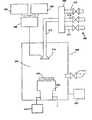
도 1은 본 명세서에 개시된 실시예들에 따른 화학적 증착 장치의 개요를 도시하는 개략도를 예시한다.
도 2는 본 명세서에 개시된 바와 같은 실시예에 따른 기판 페데스탈 모듈의 단면을 예시한다.
도 3은 본 명세서에 개시된 바와 같은 실시예에 따른 기판 페데스탈 모듈의 단면을 예시한다.Figure 1 illustrates a schematic diagram depicting an overview of a chemical vapor deposition apparatus in accordance with the embodiments disclosed herein.
2 illustrates a cross section of a substrate pedestal module according to an embodiment as disclosed herein.
3 illustrates a cross-section of a substrate pedestal module according to an embodiment as disclosed herein.
이하의 상세한 기술에서, 다수의 구체적인 실시예들은 본 명세서에 개시된 장치 및 방법들의 전체적인 이해를 제공하기 위해 제시된다. 그러나, 당업자에게 자명한 바와 같이, 본 실시예들은 이들 구체적인 상세들 없이도 또는 대안적인 엘리먼트들 또는 프로세스들을 사용함으로써 실시될 수도 있다. 다른 예들에서, 공지의 프로세스들, 절차들, 및/또는 컴포넌트들은 본 명세서에 개시된 실시예들의 양태들을 불필요하게 모호하게 하지 않도록 상세히 기술되지 않았다. 본 명세서에 사용된 바와 같이, 용어 "약"은 ± 10 %를 참조한다.In the following detailed description, numerous specific details are set forth in order to provide a thorough understanding of the apparatus and methods disclosed herein. However, as will be apparent to those skilled in the art, the embodiments may be practiced without these specific details or by using alternative elements or processes. In other instances, well-known processes, procedures, and / or components have not been described in detail so as not to unnecessarily obscure aspects of the embodiments disclosed herein. As used herein, the term " about "refers to +/- 10%.
나타낸 바와 같이, 본 실시예들은 CVD (chemical vapor deposition) 장치 또는 PECVD (plasma-enhanced chemical vapor deposition) 장치와 같은 반도체 기판 프로세싱 장치 내에서 반도체 기판을 프로세싱하기 위한 장치 및 연관된 방법들을 제공한다. 장치 및 방법들은 고온 증착 프로세스들과 같은 반도체 기판들의 고온 프로세싱과 함께 사용하는데 특히 적용가능하고, 프로세싱될 반도체 기판은 약 550 ℃ 초과의 온도들, 예컨대 약 550 ℃ 내지 약 650 ℃ 이상으로 가열된다.As shown, these embodiments provide an apparatus and associated methods for processing a semiconductor substrate in a semiconductor substrate processing apparatus, such as a chemical vapor deposition (CVD) apparatus or a plasma-enhanced chemical vapor deposition (PECVD) apparatus. The apparatus and methods are particularly applicable for use with high temperature processing of semiconductor substrates, such as high temperature deposition processes, and the semiconductor substrate to be processed is heated to temperatures above about 550 캜, such as from about 550 캜 to about 650 캜 or higher.
본 명세서에 개시된 실시예들은 플라즈마 강화된 화학적 증착 장치 (즉 PECVD 장치, PEALD 장치, 또는 PEPDL 장치) 내에서 구현되는 것이 바람직하지만, 이들로 제한되는 것은 아니다. 도 1은 본 명세서에 개시된 바와 같이 실시예들을 구현하기 위한 다양한 반도체 기판 플라즈마 프로세싱 장치 컴포넌트들을 도시하는 단순한 블록도를 제공한다. 도시된 바와 같이, 반도체 기판 플라즈마 프로세싱 장치 (300) 는 프로세싱 존 내에 플라즈마를 담도록 기능하는 진공 챔버 (324) 를 포함하고, 플라즈마는 내부에 하부 RF 전극 (미도시) 을 갖는 기판 페데스탈 모듈 (320) 과 함께 작동하는, 내부에 상부 RF 전극 (미도시) 을 갖는 샤워헤드 모듈 (314) 을 포함하는 커패시터 타입 시스템에 의해 생성된다. 적어도 하나의 RF 생성기는, 진공 챔버 (324) 내에서 플라즈마 증착 프로세스가 수행될 수도 있도록 진공 챔버 (324) 내의 반도체 기판 (316) 의 상부 표면 위의 프로세싱 존 내로 RF 에너지를 공급하고, 진공 챔버 (324) 의 프로세싱 존 내로 공급된 프로세스 가스를 에너자이징하도록 동작가능하다. 예를 들어, 고주파수 RF 생성기 (302) 및 저주파수 RF 생성기 (304) 는 각각, RF 에너지가 진공 챔버 (324) 내의 반도체 기판 (316) 위의 프로세싱 존 내로 공급될 수도 있도록 샤워헤드 모듈 (314) 의 상부 RF 전극에 연결된 매칭 네트워크 (306) 에 연결될 수도 있다.Embodiments disclosed herein are preferably, but not limited to, implemented within a plasma enhanced chemical vapor deposition apparatus (i.e., a PECVD apparatus, a PEALD apparatus, or a PEPDL apparatus). Figure 1 provides a simplified block diagram illustrating various semiconductor substrate plasma processing device components for implementing embodiments as disclosed herein. As shown, the semiconductor substrate
매칭 네트워크 (306) 에 의해 진공 챔버 (324) 의 내부로 공급된 RF 에너지의 전력 및 주파수는 프로세스 가스로부터 플라즈마를 생성하기에 충분하다. 일 실시예에서 고주파수 RF 생성기 (302) 및 저주파수 RF 생성기 (304) 양자가 사용되고, 대안적인 실시예에서, 고주파수 RF 생성기 (302) 만이 사용된다. 프로세스에서, 고주파수 RF 생성기 (302) 는 약 2 내지 100 ㎒의 주파수들; 바람직한 실시예에서 13.56 ㎒ 또는 27 ㎒에서 동작될 수도 있다. 저주파수 RF 생성기 (304) 는 약 50 ㎑ 내지 2 ㎒; 바람직한 실시예에서 약 350 내지 600 ㎑에서 동작될 수도 있다. 프로세스 파라미터들은 챔버 볼륨, 기판 사이즈, 및 다른 인자들에 기초하여 스케일링될 수도 있다. 유사하게, 프로세스 가스의 플로우 레이트들은 진공 챔버 의 자유 볼륨 또는 프로세싱 존에 따라 결정될 수도 있다.The power and frequency of the RF energy supplied into the
기판 페데스탈 모듈 (320) 의 상부 표면은 프로세싱 동안 진공 챔버 (324) 내에서 반도체 기판 (316) 을 지지한다. 기판 페데스탈 모듈 (320) 은, 증착 및/또는 플라즈마 처리 프로세스들 전, 동안 및/또는 후에 반도체 기판을 홀딩하기 위한 척 및/또는 반도체 기판을 상승 또는 하강시키기 위한 리프트 핀들을 포함할 수 있다. 대안적인 실시예에서, 기판 페데스탈 모듈 (320) 은 증착 및/또는 플라즈마 처리 프로세스들 전, 동안 및/또는 후에 반도체 기판을 상승 또는 하강시키기 위한 캐리어 링을 포함할 수 있다. 척은 정전 척, 기계 척, 또는 산업 및/또는 연구에 사용하기에 가용한 다양한 다른 타입들의 척일 수도 있다. 정전 척을 포함하는 기판 페데스탈 모듈에 대한 리프트 핀 어셈블리의 상세들은, 본 명세서에 전체가 참조로서 인용된, 공동으로 양도된 미국 특허 제 8,840,754 호에서 알 수 있다. 기판 페데스탈 모듈에 대한 캐리어 링의 상세들은 본 명세서에 전체가 참조로서 인용된, 공동으로 양도된 미국 특허 제 6,860,965 호에서 알 수 있다. 후면 가스 공급부 (341) 는 프로세싱 동안 반도체 기판의 하부 표면 아래의 영역으로 기판 페데스탈 모듈 (320) 을 통해 열 전달 가스 또는 퍼지 가스들을 공급하도록 동작가능하다. 기판 페데스탈 모듈 (320) 은 내부에 하부 RF 전극을 포함하고, 하부 RF 전극은 프로세싱 동안 접지되는 것이 바람직하지만, 대안적인 실시예에서, 프로세싱 동안 하부 RF 전극에 RF 에너지가 공급될 수도 있다.The upper surface of the
반도체 기판 플라즈마 프로세싱 장치 (300) 의 진공 챔버 (324) 내에서 반도체 기판을 프로세싱하기 위해, 프로세스 가스들은 프로세스 가스 소스 (362) 로부터 진공 챔버 (324) 내로 유입부 (312) 및 샤워헤드 모듈 (314) 을 통해 도입되고, 프로세스 가스는 막이 반도체 기판의 상부 표면 상에 증착될 수도 있도록, RF 에너지를 이용하여 플라즈마로 형성된다. 일 실시예에서, 복수의 소스 가스 라인들 (310) 은 가열된 매니폴드 (308) 에 연결될 수도 있다. 가스들은 미리 혼합되거나 챔버에 개별적으로 공급될 수도 있다. 적절한 밸브 및 질량 유량 제어 메커니즘들이 반도체 기판 프로세싱 동안 샤워헤드 모듈 (314) 을 통해 올바른 가스들이 전달된다는 것을 보장하도록 채용된다. 프로세싱 동안, 후면 열 전달 가스 또는 퍼지 가스들은 기판 페데스탈 모듈 (320) 상에 지지된 반도체 기판의 하부 표면 아래의 영역으로 공급된다. 바람직하게, 프로세싱은 CVD (chemical vapor deposition) 프로세싱, PECVD (plasma-enhanced chemical vapor deposition) 프로세싱, ALD (atomic layer deposition) 프로세싱, PEALD (plasma-enhanced atomic layer deposition) 프로세싱, PDL (pulsed deposition layer) 프로세싱, 및/또는 PEPDL (plasma-enhanced pulsed deposition layer) 프로세싱 중 적어도 하나이다.The process gases are directed from the
특정한 실시예들에서, 시스템 제어기 (162) 는 증착, 증착 후 처리들, 및/또는 다른 프로세스 동작들 동안 프로세스 조건들을 제어하도록 채용된다. 시스템 제어기 (162) 는 통상적으로 하나 이상의 메모리 디바이스들 및 하나 이상의 프로세서들을 포함할 것이다. 프로세서는 CPU 또는 컴퓨터, 아날로그 및/또는 디지털 입력/출력 접속부들, 스텝퍼 모터 제어기 보드들, 등을 포함할 수도 있다.In certain embodiments, the system controller 162 is employed to control process conditions during deposition, post-deposition processes, and / or other process operations. The system controller 162 will typically include one or more memory devices and one or more processors. The processor may include a CPU or computer, analog and / or digital input / output connections, stepper motor controller boards, and the like.
특정한 실시예들에서, 시스템 제어기 (162) 는 장치의 모든 액티비티들을 제어한다. 시스템 제어기 (162) 는 프로세싱 동작들의 타이밍, LF 발생기 (304) 및 HF 발생기 (302) 의 동작들의 주파수 및 전력, 전구체들 및 불활성 가스들의 플로우 레이트들 및 온도들 및 이들의 상대적인 혼합, 기판 페데스탈 모듈 (320) 의 상부 표면 상에 지지된 반도체 기판 (316) 의 온도, 및 샤워헤드 모듈 (314) 의 플라즈마 노출된 표면, 진공 챔버 (324) 의 압력, 및 특정한 프로세스의 다른 파라미터들을 제어하기 위한 인스트럭션들의 세트들을 포함하는 시스템 제어 소프트웨어를 실행한다. 일부 실시예들에서 제어기와 연관된 메모리 디바이스들 상에 저장된 다른 컴퓨터 프로그램들이 채용될 수도 있다.In certain embodiments, the system controller 162 controls all activities of the device. The system controller 162 controls the timing of the processing operations, the frequency and power of the operations of the
통상적으로 시스템 제어기 (162) 와 연관된 사용자 인터페이스가 있을 것이다. 사용자 인터페이스는 디스플레이 스크린, 장치 및/또는 프로세스 조건들의 그래픽 소프트웨어 디스플레이들 및 포인팅 디바이스들, 키보드들, 터치 스크린들, 마이크로폰들, 등과 같은 사용자 입력 디바이스들을 포함할 수도 있다.There will typically be a user interface associated with the system controller 162. The user interface may include user input devices such as display screens, graphical software displays of device and / or process conditions, and pointing devices, keyboards, touchscreens, microphones,
비일시적인 컴퓨터 머신-판독가능 매체가 장치의 제어를 위한 프로그램 인스트럭션들을 포함할 수 있다. 프로세싱 동작들을 제어하기 위한 컴퓨터 프로그램 코드는 예를 들어 어셈블리 언어, C, C++, 파스칼, 포트란, 또는 다른 것들과 같은 임의의 통상적인 컴퓨터 판독 가능한 프로그래밍 언어로 작성될 수 있다. 컴파일링된 객체 코드 또는 스크립트가 프로그램 내에서 식별된 태스크들을 수행하도록 프로세서에 의해서 실행된다.Non-transitory computer-machine-readable media may include program instructions for controlling the apparatus. Computer program code for controlling processing operations may be written in any conventional computer readable programming language, such as, for example, an assembly language, C, C ++, Pascal, Fortran, or others. The compiled object code or script is executed by the processor to perform tasks identified within the program.
제어기 파라미터들은 예를 들어, 프로세싱 단계들의 타이밍, 전구체들 및 불활성 가스들의 플로우 레이트들 및 온도들, 반도체 기판의 온도, 챔버의 압력 및 특정한 프로세스의 다른 파라미터들과 같은 프로세스 조건들에 관한 것이다. 이러한 파라미터들은 레시피의 형태로 사용자에게 제공되며 사용자 인터페이스를 활용하여 입력될 수도 있다.The controller parameters relate to process conditions such as, for example, the timing of the processing steps, the flow rates and temperatures of the precursors and inert gases, the temperature of the semiconductor substrate, the pressure of the chamber and other parameters of the particular process. These parameters are provided to the user in the form of a recipe and may be entered using a user interface.
프로세스를 모니터링하기 위한 신호들은 시스템 제어기의 아날로그 및/또는 디지털 입력 접속부들에 의해 제공될 수도 있다. 프로세스를 제어하기 위한 신호들은 장치의 아날로그 및 디지털 출력 접속부들 상에 출력된다.Signals for monitoring the process may be provided by analog and / or digital input connections of the system controller. Signals for controlling the process are output on the analog and digital output connections of the device.
시스템 소프트웨어는 많은 상이한 방식들로 설계되거나 구성될 수도 있다. 예를 들어, 다양한 챔버 컴포넌트 서브루틴들 또는 제어 객체들이 증착 프로세스들을 수행하는데 필요한 챔버 컴포넌트들의 동작을 제어하도록 작성될 수도 있다. 이러한 목적을 위한 프로그램들 또는 프로그램들의 섹션들의 예들은 기판 프로세싱 단계들의 타이밍 코드, 전구체들 및 불활성 가스들의 플로우 레이트들 및 온도들 코드, 및 진공 챔버 (324) 의 압력 코드를 포함한다.The system software may be designed or configured in many different ways. For example, various chamber component subroutines or control objects may be written to control the operation of chamber components required to perform deposition processes. Examples of programs or sections of programs for this purpose include the timing codes of the substrate processing steps, the flow rates and temperatures of the precursors and inert gases, and the pressure code of the
도 2 및 도 3은 본 명세서에 개시된 바와 같은 실시예들에 따른 기판 페데스탈 모듈 (320) 의 단면들을 예시한다. 도 2 및 도 3에 도시된 바와 같이, 기판 페데스탈 모듈 (320) 은 세라믹 재료로 이루어진, 반도체 기판의 프로세싱 동안 반도체 기판을 상부에 지지하는 상부 표면 (206) 을 갖는 플래튼 (205) 을 포함한다. 세라믹 재료로 이루어진 스템 (210) 은 플래튼 (205) 의 하부 표면 (208) 으로부터 하향으로 연장하고, 기판 페데스탈 모듈 (320) 이 반도체 기판 프로세싱 장치의 진공 챔버 내에 지지될 수도 있도록, 스템 (210) 은 플래튼 (205) 을 지지하는 상부 스템 플랜지 (215) 및 베이스 또는 어댑터 (미도시) 에 부착될 수도 있는 하부 스템 플랜지 (220) 를 포함한다. 기판 페데스탈 모듈 (320) 을 알루미늄 또는 알루미늄 합금과 같은 금속 재료 대신, 세라믹 재료들로 제작함으로써, 기판 페데스탈 모듈 (320) 은 약 550 ℃ 초과의 온도 또는 약 650 ℃ 초과의 온도와 같은 고온 기판 프로세싱 동안 달성된 고온을 견딜 수도 있다.Figures 2 and 3 illustrate cross-sections of a
기판 페데스탈 모듈 (320) 은 스템 (210) 의 내부 (213) 에 위치된 세라믹으로 이루어진 백사이드 가스 튜브 (250) 를 포함한다. 일 실시예에서, 백사이드 가스 튜브 (250) 는 스템 (210) 의 내부 (213) 에서 중심에 위치된다. 대안적인 실시예에서, 백사이드 가스 튜브 (250) 는 스템 (210) 의 내부에서 중심을 벗어나 (off-center) 위치된다. 백사이드 가스 튜브 (250) 는 플래튼 (205) 의 하부 표면 (208) 과 상부 스템 플랜지 (215) 의 상부 표면 사이에 위치된 상부 가스 튜브 플랜지 (253) 를 포함한다. 백사이드 가스 튜브 (250) 는, 프로세싱 동안 백사이드 가스가 백사이드 가스 튜브 (250) 및 백사이드 가스 통로 (207) 를 통해 플래튼 (205) 의 상부 표면 (206) 상에 지지된 반도체 기판의 하부 표면 아래의 영역으로 공급될 수도 있도록, 플래튼 (205) 의 적어도 하나의 백사이드 가스 통로 (207) 와 유체로 연통한다. 일 실시예에서, 상부 스템 플랜지 (215) 의 외측 직경 및 상부 가스 튜브 플랜지 (253) 의 외측 직경은 플래튼 (205) 의 외측 직경과 같거나 거의 같을 수 있다. 바람직하게, 상부 스템 플랜지 (215) 의 외측 직경 및 상부 가스 튜브 플랜지 (253) 의 외측 직경은 플래튼 (205) 의 외측 직경보다 보다 작다. 상부 스템 플랜지 (215) 의 외측 직경, 상부 가스 튜브 플랜지 (253) 의 외측 직경 및 스템 (210) 의 외측 직경, 뿐만 아니라 스템 (210) 벽의 두께는, 프로세싱 동안 대기압으로 유지되는 스템 (210) 의 내부 (213) 가 스템 (210) 의 내부 (213) 에 배치된 전기적 접속부들을 수용할뿐만 아니라 스템 (210) 을 둘러싸는 진공 압력과 스템 (210) 의 내부 (213) 의 대기압 간의 압력 차를 견딜 수 있도록, 선택된다. 바람직하게, 상부 가스 튜브 플랜지 (253) 의 외측 둘레부는 플래튼 (205) 의 외측 직경의 ¼ 이하의 반경에 위치된다.The
플래튼 (205) 은 내부에 임베딩된 적어도 하나의 정전 클램핑 전극 (209) 을 포함할 수 있고, 적어도 하나의 정전 클램핑 전극 (209) 은 프로세싱 동안 플래튼 (205) 의 상부 표면 (206) 상에 반도체 기판을 정전기적으로 클램핑하도록 동작가능하다. 도 2에 도시된 바와 같이, 플래튼 (205) 은 또한 반도체 기판의 프로세싱 동안 접지되거나 RF 전력이 공급될 수도 있는 하부 RF 전극 (265) 을 포함할 수 있다. 바람직하게, 도 3에 도시된 바와 같이, 플래튼 (205) 은 정전 클램핑 전극 및 RF 전극 양자로서 기능하는, 내부에 임베딩된 단일 전극 (209a) 만을 포함한다. 다시 도 2 및 도 3을 참조하면, 플래튼 (205) 은 또한 플래튼 (205) 의 상부 표면 (206) 에 걸친 온도 및 따라서 프로세싱 동안 반도체 기판에 걸친 온도를 제어하도록 동작가능한, 내부에 임베딩된 적어도 하나의 히터 (260) 를 포함할 수 있다. 적어도 하나의 히터 (260) 는 전기적으로 저항성 히터 막 및/또는 하나 이상의 열전 모듈을 포함할 수 있다. 바람직하게, 스템 (210) 의 내부에 배치된 적어도 하나의 정전 클램핑 전극 (209), 적어도 하나의 히터 (260), 단일 전극 (209a), 및/또는 하부 RF 전극 (265) 으로의 전기 접속부들은, 전기 접속부들이 각각의 적어도 하나의 정전 클램핑 전극 (209), 적어도 하나의 히터 (260), 단일 전극 (209a) 및/또는 하부 RF 전극 (265) 과 전기적으로 통신하는 플래튼 (205) 내에 형성된 전기적 콘택트들 (미도시) 에 각각 접속될 수도 있도록, 상부 가스 튜브 플랜지 (253) 내의 각각의 개구들 (251) 을 통해 연장한다. 이러한 방식으로, 적어도 하나의 정전 클램핑 전극 (209), 적어도 하나의 히터 (260), 단일 전극 (209a) 및/또는 하부 RF 전극 (265) 은 반도체 기판의 프로세싱 동안 전력이 공급될 수도 있다.The
일 실시예에서, 플래튼 (205) 은 함께 확산 본딩된 개별 층들을 포함할 수 있고, 적어도 하나의 정전 클램핑 전극 (209), 하부 RF 전극 (265) (또는 단일 전극 (209a)), 및 적어도 하나의 히터 (260) 은 플래튼 (205) 의 개별 층들 사이에 샌드위치될 수 있다. 플래튼 (205) 의 상부 표면 (206) 은 바람직하게 내부에 형성된 메사 패턴 (206a) 을 포함하고, 반도체 기판의 하부 표면은 메사 패턴 (206a) 상에 지지되고 후면 퍼지 가스 또는 후면 열 전달 가스는 메사 패턴 (206a) 의 메사들 사이에서 반도체 기판 아래의 영역으로 공급될 수 있다. 메사 패턴의 예시적인 실시예 및 메사 패턴을 형성하는 방법은, 전체가 본 명세서에 참조로서 인용되고, 공동으로 양도된 미국 특허 제 7,869,184 호에서 알 수 있다.In one embodiment, the
플래튼 (205), 스템 (210), 및 백사이드 가스 튜브 (250) 의 노출된 표면들은 세라믹 재료로 이루어지고, 이는 바람직하게 플래튼 (205), 스템 (210), 및/또는 백사이드 가스 튜브 (250) 가 프로세싱 조건들에 노출될 때 프로세싱 동안 기판 오염을 야기하지 않는다. 바람직하게, 플래튼 (205), 스템 (210), 및/또는 백사이드 가스 튜브 (250) 의 노출된 표면들은 알루미늄 나이트라이드로 이루어진다. 스템 (210) 의 내부 (213) 와 기판 페데스탈 모듈 (320) 이 배치되는 진공 챔버 사이에 진공 시일링을 형성하도록 상부 가스 튜브 플랜지 (253) 의 상부 표면은 바람직하게 플래튼 (205) 의 하부 표면 (208) 에 확산 본딩되고, 상부 가스 튜브 플랜지 (253) 의 하부 표면은 바람직하게 상부 스템 플랜지 (215) 의 상부 표면에 확산 본딩된다. 바람직하게, 상부 가스 튜브 플랜지 (253) 의 상부 표면과 플래튼 (205) 의 하부 표면 (208) 간의 콘택트 면적은 상부 가스 튜브 플랜지 (253) 의 하부 표면과 상부 스템 플랜지 (215) 의 상부 표면 간의 콘택트 면적과 거의 같다. 보다 바람직하게, 상부 가스 튜브 플랜지 (253) 의 상부 표면과 플래튼 (205) 의 하부 표면 (208) 간의 콘택트 면적은 상부 가스 튜브 플랜지 (253) 의 하부 표면과 상부 스템 플랜지 (215) 의 상부 표면 간의 콘택트 면적과 같다. 도 2는 상부 가스 튜브 플랜지 (253) 의 상부 표면과 플래튼 (205) 의 하부 표면 (208) 간의 콘택트 면적이 상부 가스 튜브 플랜지 (253) 의 하부 표면과 상부 스템 플랜지 (215) 의 상부 표면 간의 콘택트 면적과 같은 기판 페데스탈 모듈 (320) 의 실시예를 예시한다. 이 실시예에서, 상부 가스 튜브 플랜지 (253) 의 일부와 플래튼 (205) 의 하부 표면 (208) 사이에 갭 (230) 이 형성된다. 대안적인 실시예에서, 도 3에 도시된 바와 같이, 기판 페데스탈 모듈 (320) 은, 상부 가스 튜브 플랜지 (253) 의 상부 표면과 플래튼 (205) 의 하부 표면 (208) 사이에 갭이 없도록 형성될 수 있다.The exposed surfaces of the
추가로 기판 페데스탈 모듈 (320) 을 제작하는 방법이 본 명세서에 개시된다. 기판 페데스탈 모듈 (320) 의 제작 방법은 플래튼 (205) 의 하부 세라믹 표면 (208) 에 붙여 상부 가스 튜브 플랜지 (253) 의 상부 세라믹 표면을 위치시키는 단계를 포함한다. 상부 가스 튜브 플랜지 (253) 의 상부 세라믹 표면은 플래튼 (205) 의 하부 세라믹 표면 (208) 에 확산 본딩된다. 일 실시예에서, 상부 스템 플랜지 (215) 의 상부 세라믹 표면은 동시에 상부 가스 튜브 플랜지 (253) 의 하부 세라믹 표면에 붙여 위치되고, 상부 가스 튜브 플랜지 (253) 의 상부 세라믹 표면은, 상부 스템 플랜지 (215) 의 상부 세라믹 표면이 상부 가스 튜브 플랜지 (253) 의 하부 세라믹 표면에 확산 본딩되는 동안, 플래튼 (205) 의 하부 세라믹 표면에 동시에 확산 본딩된다. 상부 스템 플랜지 (215) 의 상부 세라믹 표면을 상부 가스 튜브 플랜지 (253) 의 하부 세라믹 표면에 그리고 상부 가스 튜브 플랜지 (253) 의 상부 세라믹 표면을 플래튼 (205) 의 하부 세라믹 표면에 동시에 확산 본딩하기 위해, 상부 스템 플랜지 (215) 의 상부 세라믹 표면과 상부 가스 튜브 플랜지 (253) 의 하부 세라믹 표면 간의 콘택트 면적뿐만 아니라 상부 가스 튜브 플랜지 (253) 의 상부 세라믹 표면과 플래튼 (205) 의 하부 세라믹 표면 (208) 간의 콘택트 면적은, 함께 확산 본딩되는 세라믹 표면들이 진공 시일링을 형성하도록 같거나 거의 같다. 이러한 방식으로, 플래튼 (205), 스템 (210), 및 백사이드 가스 튜브 (250) 는 단일 확산 본딩 프로세스에서 완전히 연결될 수 있다.A further method of fabricating the
대안적인 실시예에서, 상부 가스 튜브 플랜지 (253) 의 상부 세라믹 표면과 플래튼 (205) 의 하부 세라믹 표면 (208) 간의 콘택트 면적이 상부 가스 튜브 플랜지 (253) 의 하부 세라믹 표면과 상부 스템 플랜지 (215) 의 상부 세라믹 표면 간의 콘택트 면적과 같지 않으면, 그러면 상부 가스 튜브 플랜지 (253) 의 상부 세라믹 표면은 먼저 플래튼 (205) 의 하부 세라믹 표면 (208) 에 확산 본딩되고, 상부 스템 플랜지 (215) 의 상부 세라믹 표면은 이어서 상부 가스 튜브 플랜지 (253) 의 하부 세라믹 표면에 본딩된다.The contact area between the upper ceramic surface of the upper
반도체 기판 프로세싱 장치의 기판 페데스탈 모듈이 이의 구체적인 실시예들을 참조하여 상세히 기술되었지만, 첨부된 청구항들의 범위로부터 벗어나지 않고, 다양한 변화들 및 수정들이 이루어질 수 있고, 등가물들이 채용될 수 있다는 것이 당업자에게 자명할 것이다.Although the substrate pedestal module of a semiconductor substrate processing apparatus has been described in detail with reference to specific embodiments thereof, it will be apparent to those skilled in the art that various changes and modifications may be made, equivalents may be employed without departing from the scope of the appended claims will be.
Claims (20)
Translated fromKorean반도체 기판이 프로세싱될 수도 있는 프로세싱 존을 포함하는 진공 챔버;
상기 진공 챔버 내로 프로세스 가스를 공급하기 위해 상기 진공 챔버와 유체로 연통하는 프로세스 가스 소스;
상기 프로세스 가스 소스로부터의 프로세스 가스가 상기 진공 챔버의 상기 프로세싱 존으로 공급되는 샤워헤드 모듈; 및
프로세싱 동안 상부에 상기 반도체 기판을 지지하도록 구성된 상부 표면을 가지며 세라믹 재료로 이루어진 플래튼; 상기 플래튼을 지지하는 상부 스템 플랜지를 가지며 세라믹 재료로 이루어진 스템; 및 상기 스템의 내부에 위치되고 세라믹 재료로 이루어진 백사이드 가스 튜브를 포함하는 기판 페데스탈 모듈을 포함하고,
상기 백사이드 가스 튜브는 상기 플래튼의 하부 표면과 상기 상부 스템 플랜지의 상부 표면 사이에 위치된 상부 가스 튜브 플랜지를 포함하고, 상기 백사이드 가스 튜브는 상기 플래튼의 적어도 하나의 백사이드 가스 통로와 유체로 연통하고, 상기 백사이드 가스 튜브는 프로세싱 동안 상기 플래튼의 상기 상부 표면 상에 지지될 상기 반도체 기판의 하부 표면 아래의 영역으로 백사이드 가스를 공급하도록 구성되는, 반도체 기판 프로세싱 장치.A semiconductor substrate processing apparatus for processing semiconductor substrates,
A vacuum chamber including a processing zone in which a semiconductor substrate may be processed;
A process gas source in fluid communication with the vacuum chamber to supply a process gas into the vacuum chamber;
A showerhead module in which process gases from the process gas source are supplied to the processing zone of the vacuum chamber; And
A platen made of a ceramic material having an upper surface configured to support the semiconductor substrate at an upper portion during processing; A stem having an upper stem flange supporting the platen and made of a ceramic material; And a substrate pedestal module including a backside gas tube positioned within the stem and made of a ceramic material,
The backside gas tube comprising an upper gas tube flange positioned between a lower surface of the platen and an upper surface of the upper stem flange, the backside gas tube being in fluid communication with the at least one backside gas passage of the platen And wherein the backside gas tube is configured to supply a backside gas to an area below a lower surface of the semiconductor substrate to be supported on the upper surface of the platen during processing.
상기 반도체 기판 프로세싱 장치는,
(a) 상기 프로세싱 존 내에서 상기 프로세스 가스를 플라즈마 상태로 에너자이징 (energize) 하도록 구성된 RF 에너지 소스;
(b) 상기 반도체 기판 프로세싱 장치에 의해 수행된 프로세스들을 제어하도록 구성된 제어 시스템; 및/또는
(c) 상기 반도체 기판 프로세싱 장치의 제어를 위한 프로그램 인스트럭션들을 포함하는 비일시적인 컴퓨터 머신 판독가능 매체를 포함하는, 반도체 기판 프로세싱 장치.The method according to claim 1,
The semiconductor substrate processing apparatus comprising:
(a) an RF energy source configured to energize the process gas into a plasma state within the processing zone;
(b) a control system configured to control processes performed by the semiconductor substrate processing apparatus; And / or
(c) a non-temporary computer machine readable medium comprising program instructions for controlling the semiconductor substrate processing apparatus.
상기 스템의 상기 내부와 상기 진공 챔버 사이에 진공 시일링을 형성하도록 상기 상부 가스 튜브 플랜지의 상부 표면은 상기 플래튼의 상기 하부 표면에 확산 본딩되고 상기 상부 가스 튜브 플랜지의 하부 표면은 상기 상부 스템 플랜지의 상기 상부 표면에 확산 본딩되는, 반도체 기판 프로세싱 장치.The method according to claim 1,
Wherein an upper surface of the upper gas tube flange is diffusion bonded to the lower surface of the platen to form a vacuum seal between the interior of the stem and the vacuum chamber and the lower surface of the upper gas tube flange is bonded to the upper stem flange Wherein said top surface of said semiconductor substrate is diffusion bonded.
상기 상부 가스 튜브 플랜지의 상기 상부 표면과 상기 플래튼의 상기 하부 표면 사이의 콘택트 면적은 상기 상부 가스 튜브 플랜지의 상기 하부 표면과 상기 상부 스템 플랜지의 상기 상부 표면 사이의 콘택트 면적과 거의 같은, 반도체 기판 프로세싱 장치.The method of claim 3,
The contact area between the upper surface of the upper gas tube flange and the lower surface of the platen is substantially equal to the contact area between the lower surface of the upper gas tube flange and the upper surface of the upper stem flange, Processing device.
상기 가스 튜브 플랜지의 일부와 상기 플래튼의 상기 하부 표면 사이에 갭이 형성되거나 상기 상부 가스 튜브 플랜지의 상기 상부 표면과 상기 플래튼의 상기 하부 표면 사이에 갭이 없는, 반도체 기판 프로세싱 장치.The method according to claim 1,
Wherein a gap is formed between a portion of the gas tube flange and the lower surface of the platen or there is no gap between the upper surface of the upper gas tube flange and the lower surface of the platen.
(a) 상기 백사이드 가스 튜브, 상기 플래튼 및/또는 상기 스템은 알루미늄 나이트라이드로 형성되고;
(b) 상기 백사이드 가스 튜브는, 적어도 하나의 각각의 전기 접속부가 상기 상부 가스 튜브 플랜지를 통해 연장할 수 있도록 상기 상부 가스 튜브 플랜지 내에 적어도 하나의 개구부를 포함하고;
(c) 상기 백사이드 가스 튜브는 상기 스템의 상기 내부에서 중심에 위치되거나 상기 백사이드 가스 튜브는 상기 스템의 상기 내부에서 중심을 벗어나 (off-center) 위치되고; 그리고/또는
(d) 상기 반도체 기판 프로세싱 장치는 CVD (chemical vapor deposition) 장치, PECVD (plasma-enhanced chemical vapor deposition) 장치, ALD (atomic layer deposition) 장치, PEALD (plasma-enhanced atomic layer deposition) 장치, PDL (pulsed deposition layer) 장치, 또는 PEPDL (plasma-enhanced pulsed deposition layer) 장치인, 반도체 기판 프로세싱 장치.The method according to claim 1,
(a) the backside gas tube, the platen and / or the stem are formed of aluminum nitride;
(b) said backside gas tube includes at least one opening in said upper gas tube flange such that at least one respective electrical contact extends through said upper gas tube flange;
(c) the backside gas tube is centrally located within the interior of the stem, or the backside gas tube is located off-center within the interior of the stem; And / or
(d) The semiconductor substrate processing apparatus may be a CVD (chemical vapor deposition) apparatus, a PECVD (plasma enhanced chemical vapor deposition) apparatus, an ALD (atomic layer deposition) apparatus, a PEALD deposition layer device, or a plasma-enhanced pulsed deposition layer (PEPDL) device.
상기 기판 페데스탈 모듈은,
(a) 상기 플래튼 내에 임베딩된 적어도 하나의 정전 클램핑 전극; 또는
(b) 상기 플래튼 내에 임베딩된 하부 RF 전극; 또는
(c) 상기 플래튼 내에 임베딩된 적어도 하나의 히터; 또는
(d) 상기 플래튼의 상기 상부 표면으로 그리고 상기 상부 표면으로부터 상기 반도체 기판을 하강시키고 그리고 상승시키도록 구성된 복수의 리프트 핀들; 또는
(e) 상기 플래튼의 상기 상부 표면 상에 형성된 메사 패턴; 또는
(f) 상기 플래튼의 상기 상부 표면으로 그리고 상기 상부 표면으로부터 상기 반도체 기판을 하강시키고 그리고 상승시키도록 구성된 캐리어 링; 또는
(g) 정전 클램핑 전극 및 RF 전극으로서 기능하도록 동작가능한, 내부에 임베딩된 단일 전극을 더 포함하는, 반도체 기판 프로세싱 장치.The method according to claim 1,
Wherein the substrate pedestal module comprises:
(a) at least one electrostatic clamping electrode embedded within the platen; or
(b) a lower RF electrode embedded within the platen; or
(c) at least one heater embedded within the platen; or
(d) a plurality of lift pins configured to lower and raise the semiconductor substrate to and from the upper surface of the platen; or
(e) a mesa pattern formed on the upper surface of the platen; or
(f) a carrier ring configured to lower and raise the semiconductor substrate to and from the upper surface of the platen; or
(g) a single electrode embedded therein, operable to function as an electrostatic clamping electrode and an RF electrode.
프로세싱 동안 백사이드 가스가 상기 플래튼의 상기 상부 표면 상에 지지될 상기 반도체 기판의 상기 하부 표면 아래의 상기 영역으로 공급될 수도 있도록, 상기 플래튼의 상기 적어도 하나의 백사이드 가스 통로와 유체로 연통하는 상기 백사이드 가스 튜브를 통해 백사이드 가스를 공급하도록 동작가능한 백사이드 가스 공급부를 더 포함하는, 반도체 기판 프로세싱 장치.The method according to claim 1,
And wherein during processing, a backside gas is supplied to said area under said lower surface of said semiconductor substrate to be supported on said upper surface of said platen, said at least one backside gas passage being in fluid communication with said at least one backside gas passage of said platen. Further comprising a backside gas supply operable to supply a backside gas through the backside gas tube.
상기 상부 가스 튜브 플랜지의 외측 둘레부는 상기 플래튼의 외측 직경의 ¼ 이하의 반경에 위치되는, 반도체 기판 프로세싱 장치.The method according to claim 1,
Wherein an outer circumferential portion of the upper gas tube flange is located at a radius of less than one quarter of an outer diameter of the platen.
상기 기판 페데스탈 모듈은,
프로세싱 동안 상부에 반도체 기판을 지지하도록 구성된 상부 표면을 갖고, 세라믹으로 이루어진 플래튼;
상기 플래튼을 지지하는 상부 스템 플랜지를 갖고, 세라믹으로 이루어진 스템; 및
상기 스템의 내부에 위치된, 세라믹으로 이루어진 백사이드 가스 튜브를 포함하고,
상기 백사이드 가스 튜브는 상기 플래튼의 하부 표면과 상기 상부 스템 플랜지의 상부 표면 사이에 위치된 상부 가스 튜브 플랜지를 포함하고, 상기 백사이드 가스 튜브는 상기 플래튼의 적어도 하나의 백사이드 가스 통로와 유체로 연통하고, 상기 백사이드 가스 튜브는 프로세싱 동안 상기 플래튼의 상기 상부 표면 상에 지지될 상기 반도체 기판의 하부 표면 아래의 영역으로 백사이드 가스를 공급하도록 구성되는, 기판 페데스탈 모듈.A substrate pedestal module of a semiconductor substrate processing apparatus,
Wherein the substrate pedestal module comprises:
A platen having a top surface configured to support a semiconductor substrate on top during processing, the substrate comprising a ceramic;
A stem having an upper stem flange supporting the platen, the stem being made of ceramic; And
And a backside gas tube made of ceramic located inside the stem,
The backside gas tube comprising an upper gas tube flange positioned between a lower surface of the platen and an upper surface of the upper stem flange, the backside gas tube being in fluid communication with the at least one backside gas passage of the platen And wherein the backside gas tube is configured to supply a backside gas to an area under the lower surface of the semiconductor substrate to be supported on the upper surface of the platen during processing.
진공 시일링을 형성하도록 상기 상부 가스 튜브 플랜지의 상부 표면은 상기 플래튼의 상기 하부 표면에 확산 본딩되고 상기 상부 가스 튜브 플랜지의 하부 표면은 상기 상부 스템 플랜지의 상기 상부 표면에 확산 본딩되는, 기판 페데스탈 모듈.11. The method of claim 10,
Wherein the upper surface of the upper gas tube flange is diffusion bonded to the lower surface of the platen to form a vacuum seal ring and the lower surface of the upper gas tube flange is diffusion bonded to the upper surface of the upper stem flange. module.
상기 상부 가스 튜브 플랜지의 상기 상부 표면과 상기 플래튼의 상기 하부 표면 사이의 콘택트 면적은 상기 상부 가스 튜브 플랜지의 상기 하부 표면과 상기 상부 스템 플랜지의 상기 상부 표면 사이의 콘택트 면적과 거의 같은, 기판 페데스탈 모듈.12. The method of claim 11,
Wherein a contact area between the upper surface of the upper gas tube flange and the lower surface of the platen is substantially equal to a contact area between the lower surface of the upper gas tube flange and the upper surface of the upper stem flange, module.
상기 상부 가스 튜브 플랜지의 일부와 상기 플래튼의 상기 하부 표면 사이에 갭이 형성되거나 상기 상부 가스 튜브 플랜지의 상기 상부 표면과 상기 플래튼의 상기 하부 표면 사이에 갭이 없는, 기판 페데스탈 모듈.11. The method of claim 10,
Wherein a gap is formed between a portion of the upper gas tube flange and the lower surface of the platen or there is no gap between the upper surface of the upper gas tube flange and the lower surface of the platen.
(a) 상기 백사이드 가스 튜브, 상기 플래튼 및/또는 상기 스템은 알루미늄 나이트라이드로 형성되고;
(b) 상기 백사이드 가스 튜브는, 적어도 하나의 각각의 전기 접속부가 상기 상부 가스 튜브 플랜지를 통해 연장할 수 있도록 상기 상부 가스 튜브 플랜지 내에 적어도 하나의 개구부를 포함하고; 그리고/또는
(c) 상기 백사이드 가스 튜브는 상기 스템의 상기 내부에서 중심에 위치되거나 상기 백사이드 가스 튜브는 상기 스템의 상기 내부에서 중심을 벗어나 위치되는, 기판 페데스탈 모듈.11. The method of claim 10,
(a) the backside gas tube, the platen and / or the stem are formed of aluminum nitride;
(b) said backside gas tube includes at least one opening in said upper gas tube flange such that at least one respective electrical contact extends through said upper gas tube flange; And / or
(c) the backside gas tube is centrally located within the interior of the stem, or the backside gas tube is located off center within the interior of the stem.
상기 기판 페데스탈 모듈은,
(a) 상기 플래튼 내에 임베딩된 적어도 하나의 정전 클램핑 전극; 또는
(b) 상기 플래튼 내에 임베딩된 하부 RF 전극; 또는
(c) 상기 플래튼 내에 임베딩된 적어도 하나의 히터; 또는
(d) 상기 플래튼의 상기 상부 표면으로 그리고 상기 상부 표면으로부터 상기 반도체 기판을 하강시키고 그리고 상승시키도록 구성된 복수의 리프트 핀들; 또는
(e) 상기 플래튼의 상기 상부 표면 상에 형성된 메사 패턴; 또는
(f) 상기 플래튼의 상기 상부 표면으로 그리고 상기 상부 표면으로부터 상기 반도체 기판을 하강시키고 그리고 상승시키도록 구성된 캐리어 링; 또는
(g) 정전 클램핑 전극 및 RF 전극으로서 기능하도록 동작가능한, 내부에 임베딩된 단일 전극을 더 포함하는, 기판 페데스탈 모듈.11. The method of claim 10,
Wherein the substrate pedestal module comprises:
(a) at least one electrostatic clamping electrode embedded within the platen; or
(b) a lower RF electrode embedded within the platen; or
(c) at least one heater embedded within the platen; or
(d) a plurality of lift pins configured to lower and raise the semiconductor substrate to and from the upper surface of the platen; or
(e) a mesa pattern formed on the upper surface of the platen; or
(f) a carrier ring configured to lower and raise the semiconductor substrate to and from the upper surface of the platen; or
(g) further comprising an internally embedded single electrode operable to function as an electrostatic clamping electrode and an RF electrode.
상기 방법은,
플래튼의 하부 세라믹 표면에 붙여 (against) 상부 가스 튜브 플랜지의 상부 세라믹 표면을 위치시키는 단계; 및
진공 시일링을 형성하도록 상기 상부 가스 튜브 플랜지의 상기 상부 세라믹 표면을 상기 플래튼의 상기 하부 세라믹 표면에 확산 본딩하는 단계를 포함하는, 기판 페데스탈 모듈을 제작하는 방법.A method of fabricating a substrate pedestal module of a semiconductor substrate processing apparatus,
The method comprises:
Positioning an upper ceramic surface of the upper gas tube flange against the lower ceramic surface of the platen; And
And diffusively bonding the upper ceramic surface of the upper gas tube flange to the lower ceramic surface of the platen to form a vacuum seal ring.
상기 상부 가스 튜브 플랜지의 하부 세라믹 표면에 붙여 상부 스템 플랜지의 상부 세라믹 표면을 위치시키는 단계; 및
진공 시일링을 형성하도록 상기 상부 가스 튜브 플랜지의 상기 상부 세라믹 표면을 상기 플래튼의 상기 하부 세라믹 표면에 그리고 상기 상부 스템 플랜지의 상기 상부 세라믹 표면을 상기 상부 가스 튜브 플랜지의 상기 하부 세라믹 표면에 동시에 확산 본딩하거나, 상기 상부 가스 튜브 플랜지의 상기 상부 세라믹 표면을 상기 플래튼의 상기 하부 세라믹 표면에 확산 본딩한 후 진공 시일링을 형성하도록 상기 상부 스템 플랜지의 상기 상부 세라믹 표면을 상기 상부 가스 튜브 플랜지의 상기 하부 세라믹 표면에 확산 본딩하는 단계를 더 포함하는, 기판 페데스탈 모듈을 제작하는 방법.17. The method of claim 16,
Positioning an upper ceramic surface of the upper stem flange on the lower ceramic surface of the upper gas tube flange; And
The upper ceramic surface of the upper gas tube flange is simultaneously diffused to the lower ceramic surface of the platen and the upper ceramic surface of the upper stem flange to the lower ceramic surface of the upper gas tube flange to form a vacuum seal ring Bonding the upper ceramic surface of the upper stem flange to the lower ceramic surface of the platen and then bonding the upper ceramic surface of the upper gas tube flange to the lower ceramic surface of the platen to form a vacuum seal ring, Further comprising diffusion bonding to a lower ceramic surface. ≪ Desc / Clms Page number 20 >
상기 프로세스 가스를 상기 프로세스 가스 소스로부터 상기 프로세싱 존 내로 공급하는 단계; 및
상기 플래튼의 상기 상부 표면 상에 지지된 반도체 기판을 프로세싱하는 단계를 포함하는, 반도체 기판을 프로세싱하기 위한 방법.A method for processing a semiconductor substrate in the semiconductor substrate processing apparatus of claim 1,
Supplying the process gas from the process gas source into the processing zone; And
And processing the semiconductor substrate supported on the upper surface of the platen.
프로세싱 동안 상기 플래튼의 상기 상부 표면 상에 지지된 상기 반도체 기판의 하부 표면 아래의 영역으로 상기 백사이드 가스 튜브를 통해 백사이드 열 전달 가스 또는 퍼지 가스를 공급하는 단계를 더 포함하는, 반도체 기판을 프로세싱하기 위한 방법.19. The method of claim 18,
Further comprising supplying a backside heat transfer gas or purge gas through the backside gas tube to an area below the lower surface of the semiconductor substrate supported on the upper surface of the platen during processing. Way.
상기 프로세싱은 CVD (chemical vapor deposition), PECVD (plasma-enhanced chemical vapor deposition), ALD (atomic layer deposition), PEALD (plasma-enhanced atomic layer deposition), PDL (pulsed deposition layer), 및/또는 PEPDL (plasma-enhanced pulsed deposition layer) 중 적어도 하나인, 반도체 기판을 프로세싱하기 위한 방법.19. The method of claim 18,
The processing may be performed by a variety of techniques including, but not limited to, chemical vapor deposition (CVD), plasma enhanced chemical vapor deposition (PECVD), atomic layer deposition (ALD), plasma enhanced atomic layer deposition (PEALD), pulsed deposition layer -enhanced pulsed deposition layer. < / RTI >
Priority Applications (1)
| Application Number | Priority Date | Filing Date | Title |
|---|---|---|---|
| KR1020240025363AKR20240031982A (en) | 2015-05-12 | 2024-02-21 | Substrate pedestal module including backside gas delivery tube and method of making |
Applications Claiming Priority (2)
| Application Number | Priority Date | Filing Date | Title |
|---|---|---|---|
| US14/710,132 | 2015-05-12 | ||
| US14/710,132US9738975B2 (en) | 2015-05-12 | 2015-05-12 | Substrate pedestal module including backside gas delivery tube and method of making |
Related Child Applications (1)
| Application Number | Title | Priority Date | Filing Date |
|---|---|---|---|
| KR1020240025363ADivisionKR20240031982A (en) | 2015-05-12 | 2024-02-21 | Substrate pedestal module including backside gas delivery tube and method of making |
Publications (2)
| Publication Number | Publication Date |
|---|---|
| KR20160133373Atrue KR20160133373A (en) | 2016-11-22 |
| KR102641003B1 KR102641003B1 (en) | 2024-02-23 |
Family
ID=57276852
Family Applications (2)
| Application Number | Title | Priority Date | Filing Date |
|---|---|---|---|
| KR1020160057390AActiveKR102641003B1 (en) | 2015-05-12 | 2016-05-11 | Substrate pedestal module including backside gas delivery tube and method of making |
| KR1020240025363APendingKR20240031982A (en) | 2015-05-12 | 2024-02-21 | Substrate pedestal module including backside gas delivery tube and method of making |
Family Applications After (1)
| Application Number | Title | Priority Date | Filing Date |
|---|---|---|---|
| KR1020240025363APendingKR20240031982A (en) | 2015-05-12 | 2024-02-21 | Substrate pedestal module including backside gas delivery tube and method of making |
Country Status (4)
| Country | Link |
|---|---|
| US (4) | US9738975B2 (en) |
| JP (2) | JP6815745B2 (en) |
| KR (2) | KR102641003B1 (en) |
| CN (2) | CN112063995B (en) |
Cited By (5)
| Publication number | Priority date | Publication date | Assignee | Title |
|---|---|---|---|---|
| KR20180131423A (en)* | 2017-05-30 | 2018-12-10 | 램 리써치 코포레이션 | Substrate pedestal module including metallized ceramic tubes for rf and gas delivery |
| CN110088885A (en)* | 2016-12-14 | 2019-08-02 | 朗姆研究公司 | Thermally Controlled Integrated Showerhead Delivering Radical and Precursor Gases to Downstream Chambers for Remote Plasma Film Deposition |
| US10655225B2 (en) | 2015-05-12 | 2020-05-19 | Lam Research Corporation | Substrate pedestal module including backside gas delivery tube and method of making |
| WO2022075759A1 (en)* | 2020-10-08 | 2022-04-14 | 주식회사 메카로 | Pedestal heater block having asymmetric heating wire structure |
| US12116669B2 (en) | 2017-12-08 | 2024-10-15 | Lam Research Corporation | Integrated showerhead with improved hole pattern for delivering radical and precursor gas to a downstream chamber to enable remote plasma film deposition |
Families Citing this family (21)
| Publication number | Priority date | Publication date | Assignee | Title |
|---|---|---|---|---|
| US10177024B2 (en)* | 2015-05-12 | 2019-01-08 | Lam Research Corporation | High temperature substrate pedestal module and components thereof |
| JP2017077528A (en)* | 2015-10-20 | 2017-04-27 | 信越化学工業株式会社 | Substrate cleaning device and substrate cleaning method used in photomask-related substrate |
| US11289355B2 (en)* | 2017-06-02 | 2022-03-29 | Lam Research Corporation | Electrostatic chuck for use in semiconductor processing |
| US11004722B2 (en)* | 2017-07-20 | 2021-05-11 | Applied Materials, Inc. | Lift pin assembly |
| US11469084B2 (en) | 2017-09-05 | 2022-10-11 | Lam Research Corporation | High temperature RF connection with integral thermal choke |
| KR102300756B1 (en)* | 2017-11-21 | 2021-09-10 | 와틀로 일렉트릭 매뉴팩츄어링 컴파니 | Ceramic pedestal with atomic protective layer |
| US11990360B2 (en) | 2018-01-31 | 2024-05-21 | Lam Research Corporation | Electrostatic chuck (ESC) pedestal voltage isolation |
| US11086233B2 (en) | 2018-03-20 | 2021-08-10 | Lam Research Corporation | Protective coating for electrostatic chucks |
| US11183368B2 (en) | 2018-08-02 | 2021-11-23 | Lam Research Corporation | RF tuning systems including tuning circuits having impedances for setting and adjusting parameters of electrodes in electrostatic chucks |
| US11715652B2 (en)* | 2018-09-28 | 2023-08-01 | Ngk Insulators, Ltd. | Member for semiconductor manufacturing apparatus |
| CN109594063A (en)* | 2018-12-27 | 2019-04-09 | 西安奕斯伟硅片技术有限公司 | A kind of extension consersion unit |
| DE102019101657A1 (en)* | 2019-01-23 | 2020-07-23 | Berliner Glas Kgaa Herbert Kubatz Gmbh & Co | Holding device for electrostatically holding a component with a base body joined by diffusion bonding and method for its production |
| FI129040B (en) | 2019-06-06 | 2021-05-31 | Picosun Oy | Coating of fluid-permeable materials |
| WO2021145110A1 (en)* | 2020-01-15 | 2021-07-22 | 日本特殊陶業株式会社 | Holding device |
| KR20250033324A (en) | 2020-02-11 | 2025-03-07 | 램 리써치 코포레이션 | Carrier ring designs for controlling deposition on wafer bevel/edge |
| US11699602B2 (en)* | 2020-07-07 | 2023-07-11 | Applied Materials, Inc. | Substrate support assemblies and components |
| WO2022093273A1 (en)* | 2020-10-30 | 2022-05-05 | Applied Materials, Inc. | Rf delivery and feedthrough assembly to a processing chamber |
| US20240175134A1 (en)* | 2021-03-25 | 2024-05-30 | Lam Research Corporation | Conductive cooling of a low temperature pedestal operating in a high temperature deposition sequence |
| WO2023034760A1 (en)* | 2021-09-02 | 2023-03-09 | Lam Research Corporation | Joining techniques for composite ceramic bodies |
| US20240355593A1 (en)* | 2023-04-18 | 2024-10-24 | Tokyo Electron Limited | Electrostatic Chuck and Method of Operation for Plasma Processing |
| US12412769B2 (en)* | 2023-05-16 | 2025-09-09 | Applied Materials, Inc. | Electrostatic chucks with hybrid pucks to improve thermal performance and leakage current stability |
Citations (4)
| Publication number | Priority date | Publication date | Assignee | Title |
|---|---|---|---|---|
| JP2002110774A (en)* | 2000-06-09 | 2002-04-12 | Applied Materials Inc | Temperature control electrostatic chuck for whole area and manufacturing method thereof |
| US20030136520A1 (en)* | 2002-01-22 | 2003-07-24 | Applied Materials, Inc. | Ceramic substrate support |
| KR20040038753A (en)* | 2002-10-29 | 2004-05-08 | 닛폰 하츠죠 가부시키가이샤 | Apparatus for vapor deposition |
| JP2007165322A (en)* | 2006-12-15 | 2007-06-28 | Kyocera Corp | Sample heating apparatus and manufacturing method thereof |
Family Cites Families (66)
| Publication number | Priority date | Publication date | Assignee | Title |
|---|---|---|---|---|
| JPH07153706A (en) | 1993-05-27 | 1995-06-16 | Applied Materials Inc | Susceptor device |
| EP0628644B1 (en) | 1993-05-27 | 2003-04-02 | Applied Materials, Inc. | Improvements in or relating to susceptors suitable for use in chemical vapour deposition devices |
| US6544379B2 (en)* | 1993-09-16 | 2003-04-08 | Hitachi, Ltd. | Method of holding substrate and substrate holding system |
| US5569356A (en) | 1995-05-19 | 1996-10-29 | Lam Research Corporation | Electrode clamping assembly and method for assembly and use thereof |
| US6035101A (en) | 1997-02-12 | 2000-03-07 | Applied Materials, Inc. | High temperature multi-layered alloy heater assembly and related methods |
| US6616767B2 (en) | 1997-02-12 | 2003-09-09 | Applied Materials, Inc. | High temperature ceramic heater assembly with RF capability |
| JP3641115B2 (en)* | 1997-10-08 | 2005-04-20 | 大日本スクリーン製造株式会社 | Substrate processing equipment |
| US6103074A (en)* | 1998-02-14 | 2000-08-15 | Phygen, Inc. | Cathode arc vapor deposition method and apparatus |
| US6464795B1 (en)* | 1999-05-21 | 2002-10-15 | Applied Materials, Inc. | Substrate support member for a processing chamber |
| US6223447B1 (en) | 2000-02-15 | 2001-05-01 | Applied Materials, Inc. | Fastening device for a purge ring |
| US6494955B1 (en)* | 2000-02-15 | 2002-12-17 | Applied Materials, Inc. | Ceramic substrate support |
| JP4398064B2 (en)* | 2000-05-12 | 2010-01-13 | 日本発條株式会社 | Heating device |
| US6860965B1 (en) | 2000-06-23 | 2005-03-01 | Novellus Systems, Inc. | High throughput architecture for semiconductor processing |
| US6997993B2 (en) | 2001-02-09 | 2006-02-14 | Ngk Insulators, Ltd. | Susceptor supporting construction |
| WO2002083596A1 (en)* | 2001-04-13 | 2002-10-24 | Sumitomo Electric Industries, Ltd. | Joined ceramic article, substrate holding structure and apparatus for treating substrate |
| JP3520074B2 (en) | 2002-03-28 | 2004-04-19 | 日本碍子株式会社 | Ceramic susceptor mounting structure, ceramic susceptor support structure, and ceramic susceptor support member |
| US6962348B2 (en) | 2002-07-29 | 2005-11-08 | Tokyo Electron Limited | Sealing apparatus having a single groove |
| US7126808B2 (en) | 2003-04-01 | 2006-10-24 | Varian Semiconductor Equipment Associates, Inc. | Wafer platen equipped with electrostatic clamp, wafer backside gas cooling, and high voltage operation capability for plasma doping |
| US7645341B2 (en) | 2003-12-23 | 2010-01-12 | Lam Research Corporation | Showerhead electrode assembly for plasma processing apparatuses |
| JP4365766B2 (en)* | 2004-10-26 | 2009-11-18 | 京セラ株式会社 | Wafer support member and semiconductor manufacturing apparatus using the same |
| US7126093B2 (en)* | 2005-02-23 | 2006-10-24 | Ngk Insulators, Ltd. | Heating systems |
| JP4590364B2 (en)* | 2005-03-16 | 2010-12-01 | 日本碍子株式会社 | Processing equipment |
| JP4590363B2 (en)* | 2005-03-16 | 2010-12-01 | 日本碍子株式会社 | Gas supply member and processing apparatus using the same |
| US20060231388A1 (en)* | 2005-04-14 | 2006-10-19 | Ravi Mullapudi | Multi-station sputtering and cleaning system |
| JP2007051317A (en) | 2005-08-16 | 2007-03-01 | Ngk Insulators Ltd | Heating device |
| CN101243542B (en)* | 2005-08-17 | 2011-02-09 | 应用材料股份有限公司 | Substrate support with weld plate and heater |
| US7869184B2 (en) | 2005-11-30 | 2011-01-11 | Lam Research Corporation | Method of determining a target mesa configuration of an electrostatic chuck |
| KR100804169B1 (en)* | 2005-12-31 | 2008-02-18 | 주식회사 아이피에스 | Susceptor for Thin Film Deposition Chamber |
| US20070169703A1 (en) | 2006-01-23 | 2007-07-26 | Brent Elliot | Advanced ceramic heater for substrate processing |
| US7737035B1 (en) | 2006-03-31 | 2010-06-15 | Novellus Systems, Inc. | Dual seal deposition process chamber and process |
| JP4762098B2 (en)* | 2006-09-28 | 2011-08-31 | 大日本スクリーン製造株式会社 | Substrate processing apparatus and substrate processing method |
| US8294069B2 (en) | 2007-03-28 | 2012-10-23 | Ngk Insulators, Ltd. | Heating device for heating a wafer |
| JP5135915B2 (en)* | 2007-06-28 | 2013-02-06 | 東京エレクトロン株式会社 | Mounting table structure and heat treatment apparatus |
| JP2009054871A (en)* | 2007-08-28 | 2009-03-12 | Tokyo Electron Ltd | Placing stand structure and treatment apparatus |
| JP4450106B1 (en)* | 2008-03-11 | 2010-04-14 | 東京エレクトロン株式会社 | Mounting table structure and processing device |
| US8540819B2 (en)* | 2008-03-21 | 2013-09-24 | Ngk Insulators, Ltd. | Ceramic heater |
| US20090277388A1 (en)* | 2008-05-09 | 2009-11-12 | Applied Materials, Inc. | Heater with detachable shaft |
| JP5349232B2 (en)* | 2009-09-17 | 2013-11-20 | 株式会社ニューフレアテクノロジー | Film forming apparatus and film forming method |
| DE102009044276A1 (en)* | 2009-10-16 | 2011-05-05 | Aixtron Ag | CVD reactor with multi-zone gas cushion substrate holder |
| JP5960384B2 (en) | 2009-10-26 | 2016-08-02 | 新光電気工業株式会社 | Electrostatic chuck substrate and electrostatic chuck |
| SG183432A1 (en)* | 2010-02-24 | 2012-09-27 | Veeco Instr Inc | Processing methods and apparatus with temperature distribution control |
| KR20110136583A (en)* | 2010-06-15 | 2011-12-21 | 삼성엘이디 주식회사 | Susceptor and chemical vapor deposition apparatus having the same |
| JP5791412B2 (en)* | 2010-07-26 | 2015-10-07 | 日本碍子株式会社 | Ceramic heater |
| KR20120014361A (en)* | 2010-08-09 | 2012-02-17 | 삼성엘이디 주식회사 | Susceptor and chemical vapor deposition apparatus including the same |
| US8840754B2 (en) | 2010-09-17 | 2014-09-23 | Lam Research Corporation | Polar regions for electrostatic de-chucking with lift pins |
| WO2012039453A1 (en)* | 2010-09-24 | 2012-03-29 | 日本碍子株式会社 | Member for semiconductor manufacturing apparatus |
| JP2012182221A (en) | 2011-02-28 | 2012-09-20 | Taiheiyo Cement Corp | Substrate supporting member |
| US8801950B2 (en) | 2011-03-07 | 2014-08-12 | Novellus Systems, Inc. | Reduction of a process volume of a processing chamber using a nested dynamic inert volume |
| US8371567B2 (en) | 2011-04-13 | 2013-02-12 | Novellus Systems, Inc. | Pedestal covers |
| US8979087B2 (en)* | 2011-07-29 | 2015-03-17 | Applied Materials, Inc. | Substrate supporting edge ring with coating for improved soak performance |
| US10224182B2 (en) | 2011-10-17 | 2019-03-05 | Novellus Systems, Inc. | Mechanical suppression of parasitic plasma in substrate processing chamber |
| DE102012205616B4 (en)* | 2012-04-04 | 2016-07-14 | Siltronic Ag | Device for depositing a layer on a semiconductor wafer by means of vapor deposition |
| US9490150B2 (en)* | 2012-07-03 | 2016-11-08 | Applied Materials, Inc. | Substrate support for substrate backside contamination control |
| US9088085B2 (en) | 2012-09-21 | 2015-07-21 | Novellus Systems, Inc. | High temperature electrode connections |
| WO2014073554A1 (en) | 2012-11-06 | 2014-05-15 | 日本碍子株式会社 | Susceptor |
| US8941969B2 (en)* | 2012-12-21 | 2015-01-27 | Applied Materials, Inc. | Single-body electrostatic chuck |
| US10125422B2 (en) | 2013-03-27 | 2018-11-13 | Applied Materials, Inc. | High impedance RF filter for heater with impedance tuning device |
| US10808317B2 (en) | 2013-07-03 | 2020-10-20 | Lam Research Corporation | Deposition apparatus including an isothermal processing zone |
| US9558981B2 (en)* | 2013-11-19 | 2017-01-31 | Applied Materials, Inc. | Control systems employing deflection sensors to control clamping forces applied by electrostatic chucks, and related methods |
| WO2015146563A1 (en)* | 2014-03-27 | 2015-10-01 | 日本碍子株式会社 | Joined structure between ceramic plate and metallic cylindrical member |
| US10266943B2 (en)* | 2014-06-27 | 2019-04-23 | Applied Materials, Inc. | Plasma corrosion resistive heater for high temperature processing |
| TWI654332B (en)* | 2014-07-02 | 2019-03-21 | 美商應用材料股份有限公司 | Multi-zone pedestal for plasma processing |
| US9728437B2 (en)* | 2015-02-03 | 2017-08-08 | Applied Materials, Inc. | High temperature chuck for plasma processing systems |
| US10177024B2 (en)* | 2015-05-12 | 2019-01-08 | Lam Research Corporation | High temperature substrate pedestal module and components thereof |
| US9738975B2 (en) | 2015-05-12 | 2017-08-22 | Lam Research Corporation | Substrate pedestal module including backside gas delivery tube and method of making |
| US10147610B1 (en)* | 2017-05-30 | 2018-12-04 | Lam Research Corporation | Substrate pedestal module including metallized ceramic tubes for RF and gas delivery |
- 2015
- 2015-05-12USUS14/710,132patent/US9738975B2/enactiveActive
- 2016
- 2016-05-02JPJP2016092266Apatent/JP6815745B2/enactiveActive
- 2016-05-11KRKR1020160057390Apatent/KR102641003B1/enactiveActive
- 2016-05-12CNCN202010719108.1Apatent/CN112063995B/enactiveActive
- 2016-05-12CNCN201610312750.1Apatent/CN106148915B/enactiveActive
- 2017
- 2017-07-28USUS15/662,553patent/US10655225B2/enactiveActive
- 2020
- 2020-04-30USUS16/863,835patent/US11634817B2/enactiveActive
- 2020-12-23JPJP2020213139Apatent/JP7168642B2/enactiveActive
- 2023
- 2023-03-17USUS18/123,153patent/US12398464B2/enactiveActive
- 2024
- 2024-02-21KRKR1020240025363Apatent/KR20240031982A/enactivePending
Patent Citations (5)
| Publication number | Priority date | Publication date | Assignee | Title |
|---|---|---|---|---|
| JP2002110774A (en)* | 2000-06-09 | 2002-04-12 | Applied Materials Inc | Temperature control electrostatic chuck for whole area and manufacturing method thereof |
| US20030136520A1 (en)* | 2002-01-22 | 2003-07-24 | Applied Materials, Inc. | Ceramic substrate support |
| KR20040038753A (en)* | 2002-10-29 | 2004-05-08 | 닛폰 하츠죠 가부시키가이샤 | Apparatus for vapor deposition |
| US20040194710A1 (en)* | 2002-10-29 | 2004-10-07 | Nhk Spring Co., Ltd. | Apparatus for vapor deposition |
| JP2007165322A (en)* | 2006-12-15 | 2007-06-28 | Kyocera Corp | Sample heating apparatus and manufacturing method thereof |
Cited By (12)
| Publication number | Priority date | Publication date | Assignee | Title |
|---|---|---|---|---|
| US10655225B2 (en) | 2015-05-12 | 2020-05-19 | Lam Research Corporation | Substrate pedestal module including backside gas delivery tube and method of making |
| US11634817B2 (en) | 2015-05-12 | 2023-04-25 | Lam Research Corporation | Substrate pedestal including backside gas-delivery tube |
| US12398464B2 (en) | 2015-05-12 | 2025-08-26 | Lam Research Corporation | Substrate pedestal including backside gas-delivery tube |
| CN110088885A (en)* | 2016-12-14 | 2019-08-02 | 朗姆研究公司 | Thermally Controlled Integrated Showerhead Delivering Radical and Precursor Gases to Downstream Chambers for Remote Plasma Film Deposition |
| US11608559B2 (en) | 2016-12-14 | 2023-03-21 | Lam Research Corporation | Integrated showerhead with thermal control for delivering radical and precursor gas to a downstream chamber to enable remote plasma film deposition |
| CN110088885B (en)* | 2016-12-14 | 2023-10-13 | 朗姆研究公司 | Thermally controlled integrated showerhead delivering radicals and precursor gases to downstream chamber for remote plasma film deposition |
| US12000047B2 (en) | 2016-12-14 | 2024-06-04 | Lam Research Corporation | Integrated showerhead with thermal control for delivering radical and precursor gas to a downstream chamber to enable remote plasma film deposition |
| US12331402B2 (en) | 2016-12-14 | 2025-06-17 | Lam Research Corporation | Integrated showerhead with thermal control for delivering radical and precursor gas to a downstream chamber to enable remote plasma film deposition |
| KR20180131423A (en)* | 2017-05-30 | 2018-12-10 | 램 리써치 코포레이션 | Substrate pedestal module including metallized ceramic tubes for rf and gas delivery |
| US12116669B2 (en) | 2017-12-08 | 2024-10-15 | Lam Research Corporation | Integrated showerhead with improved hole pattern for delivering radical and precursor gas to a downstream chamber to enable remote plasma film deposition |
| WO2022075759A1 (en)* | 2020-10-08 | 2022-04-14 | 주식회사 메카로 | Pedestal heater block having asymmetric heating wire structure |
| KR20220046921A (en)* | 2020-10-08 | 2022-04-15 | 주식회사 메카로 | pedestal heater block having asymmetric heater line structure |
Also Published As
| Publication number | Publication date |
|---|---|
| KR20240031982A (en) | 2024-03-08 |
| CN112063995B (en) | 2023-06-27 |
| US20200325578A1 (en) | 2020-10-15 |
| CN106148915A (en) | 2016-11-23 |
| JP2016213456A (en) | 2016-12-15 |
| KR102641003B1 (en) | 2024-02-23 |
| JP7168642B2 (en) | 2022-11-09 |
| US9738975B2 (en) | 2017-08-22 |
| US11634817B2 (en) | 2023-04-25 |
| US20230220549A1 (en) | 2023-07-13 |
| US20160333475A1 (en) | 2016-11-17 |
| US12398464B2 (en) | 2025-08-26 |
| US20170321324A1 (en) | 2017-11-09 |
| JP2021061422A (en) | 2021-04-15 |
| CN106148915B (en) | 2020-08-21 |
| JP6815745B2 (en) | 2021-01-20 |
| CN112063995A (en) | 2020-12-11 |
| US10655225B2 (en) | 2020-05-19 |
Similar Documents
| Publication | Publication Date | Title |
|---|---|---|
| US12398464B2 (en) | Substrate pedestal including backside gas-delivery tube | |
| KR102762677B1 (en) | High temperature substrate pedestal module and components thereof | |
| US10253412B2 (en) | Deposition apparatus including edge plenum showerhead assembly | |
| JP7271443B2 (en) | Electrostatic chuck for use in semiconductor processing | |
| KR20150002543A (en) | Chemical deposition chamber having gas seal | |
| KR20150071683A (en) | Seminconductor substrate processing apparatus including uniformity baffles | |
| TWI868316B (en) | Plasma processing apparatus | |
| TW202303825A (en) | Substrate support and substrate processing device |
Legal Events
| Date | Code | Title | Description |
|---|---|---|---|
| PA0109 | Patent application | Patent event code:PA01091R01D Comment text:Patent Application Patent event date:20160511 | |
| PG1501 | Laying open of application | ||
| A201 | Request for examination | ||
| PA0201 | Request for examination | Patent event code:PA02012R01D Patent event date:20210510 Comment text:Request for Examination of Application Patent event code:PA02011R01I Patent event date:20160511 Comment text:Patent Application | |
| E902 | Notification of reason for refusal | ||
| PE0902 | Notice of grounds for rejection | Comment text:Notification of reason for refusal Patent event date:20221115 Patent event code:PE09021S01D | |
| E902 | Notification of reason for refusal | ||
| PE0902 | Notice of grounds for rejection | Comment text:Notification of reason for refusal Patent event date:20230528 Patent event code:PE09021S01D | |
| E701 | Decision to grant or registration of patent right | ||
| PE0701 | Decision of registration | Patent event code:PE07011S01D Comment text:Decision to Grant Registration Patent event date:20231122 | |
| GRNT | Written decision to grant | ||
| PR0701 | Registration of establishment | Comment text:Registration of Establishment Patent event date:20240221 Patent event code:PR07011E01D | |
| PR1002 | Payment of registration fee | Payment date:20240221 End annual number:3 Start annual number:1 | |
| PG1601 | Publication of registration |