KR20160130643A - Insert for test handler - Google Patents
Insert for test handlerDownload PDFInfo
- Publication number
- KR20160130643A KR20160130643AKR1020150062674AKR20150062674AKR20160130643AKR 20160130643 AKR20160130643 AKR 20160130643AKR 1020150062674 AKR1020150062674 AKR 1020150062674AKR 20150062674 AKR20150062674 AKR 20150062674AKR 20160130643 AKR20160130643 AKR 20160130643A
- Authority
- KR
- South Korea
- Prior art keywords
- semiconductor element
- insert
- guide grooves
- specific
- insertion hole
- Prior art date
- Legal status (The legal status is an assumption and is not a legal conclusion. Google has not performed a legal analysis and makes no representation as to the accuracy of the status listed.)
- Granted
Links
- 238000012360testing methodMethods0.000titleclaimsabstractdescription66
- 239000004065semiconductorSubstances0.000claimsabstractdescription127
- 238000000926separation methodMethods0.000claimsabstractdescription5
- 238000003780insertionMethods0.000claimsdescription26
- 230000037431insertionEffects0.000claimsdescription26
- 238000000034methodMethods0.000claimsdescription5
- 230000014759maintenance of locationEffects0.000abstractdescription2
- 238000004519manufacturing processMethods0.000description3
- 238000010586diagramMethods0.000description1
- 238000006073displacement reactionMethods0.000description1
- 230000000694effectsEffects0.000description1
- 230000007613environmental effectEffects0.000description1
- 230000005281excited stateEffects0.000description1
- 230000010354integrationEffects0.000description1
- 230000002452interceptive effectEffects0.000description1
- 238000003032molecular dockingMethods0.000description1
Images


Classifications
- G—PHYSICS
- G01—MEASURING; TESTING
- G01R—MEASURING ELECTRIC VARIABLES; MEASURING MAGNETIC VARIABLES
- G01R31/00—Arrangements for testing electric properties; Arrangements for locating electric faults; Arrangements for electrical testing characterised by what is being tested not provided for elsewhere
- G01R31/28—Testing of electronic circuits, e.g. by signal tracer
- G01R31/2851—Testing of integrated circuits [IC]
- G01R31/2893—Handling, conveying or loading, e.g. belts, boats, vacuum fingers
- G—PHYSICS
- G01—MEASURING; TESTING
- G01R—MEASURING ELECTRIC VARIABLES; MEASURING MAGNETIC VARIABLES
- G01R31/00—Arrangements for testing electric properties; Arrangements for locating electric faults; Arrangements for electrical testing characterised by what is being tested not provided for elsewhere
- G01R31/26—Testing of individual semiconductor devices
- G01R31/2601—Apparatus or methods therefor
- B—PERFORMING OPERATIONS; TRANSPORTING
- B07—SEPARATING SOLIDS FROM SOLIDS; SORTING
- B07C—POSTAL SORTING; SORTING INDIVIDUAL ARTICLES, OR BULK MATERIAL FIT TO BE SORTED PIECE-MEAL, e.g. BY PICKING
- B07C5/00—Sorting according to a characteristic or feature of the articles or material being sorted, e.g. by control effected by devices which detect or measure such characteristic or feature; Sorting by manually actuated devices, e.g. switches
- B07C5/34—Sorting according to other particular properties
- G—PHYSICS
- G01—MEASURING; TESTING
- G01R—MEASURING ELECTRIC VARIABLES; MEASURING MAGNETIC VARIABLES
- G01R31/00—Arrangements for testing electric properties; Arrangements for locating electric faults; Arrangements for electrical testing characterised by what is being tested not provided for elsewhere
- G01R31/26—Testing of individual semiconductor devices
- G01R31/27—Testing of devices without physical removal from the circuit of which they form part, e.g. compensating for effects surrounding elements
- G01R31/275—Testing of devices without physical removal from the circuit of which they form part, e.g. compensating for effects surrounding elements for testing individual semiconductor components within integrated circuits
- G—PHYSICS
- G01—MEASURING; TESTING
- G01R—MEASURING ELECTRIC VARIABLES; MEASURING MAGNETIC VARIABLES
- G01R31/00—Arrangements for testing electric properties; Arrangements for locating electric faults; Arrangements for electrical testing characterised by what is being tested not provided for elsewhere
- G01R31/28—Testing of electronic circuits, e.g. by signal tracer
- G01R31/2851—Testing of integrated circuits [IC]
- G01R31/2855—Environmental, reliability or burn-in testing
- G01R31/286—External aspects, e.g. related to chambers, contacting devices or handlers
Landscapes
- Engineering & Computer Science (AREA)
- Physics & Mathematics (AREA)
- General Physics & Mathematics (AREA)
- Microelectronics & Electronic Packaging (AREA)
- Computer Hardware Design (AREA)
- General Engineering & Computer Science (AREA)
- Environmental & Geological Engineering (AREA)
- Testing Of Individual Semiconductor Devices (AREA)
Abstract
Translated fromKoreanDescription
Translated fromKorean본 발명은 테스트핸들러에서 반도체소자를 적재시킬 수 있는 테스트트레이의 인서트에 관한 것이다.
The present invention relates to an insert of a test tray capable of loading semiconductor elements in a test handler.
테스트핸들러는 소정의 제조공정을 거쳐 제조된 반도체소자들을 고객트레이(CUSTOMER TRAY)로부터 테스트트레이(TEST TRAY)로 이동시킨 후, 테스트트레이에 적재되어 있는 반도체소자들이 동시에 테스터(TESTER)에 의해 테스트(TEST)될 수 있도록 지원하며, 테스트 결과에 따라 반도체소자를 등급별로 분류하면서 테스트트레이에서 고객트레이로 이동시키는 기기로서 이미 다수의 공개문서들을 통해 공개되어 있다.The test handler moves semiconductor devices manufactured through a predetermined manufacturing process from a customer tray to a test tray and then tests the semiconductor devices loaded on the test tray by a tester at the same time TEST), and it is a device that moves test trays from the test tray to the customer tray by classifying the semiconductor devices according to the test result, and is already disclosed through a plurality of public documents.
대한민국 특허출원 10-2012-0089602호(발명의 명칭 : 테스핸들러용 인서트, 이하 '선행기술1'이라 함)나 대한민국 특허출원 10-2012-0107985호(발명의 명칭 : 테스트핸들러용 인서트, 이하 '선행기술2'라 함) 등에서 참조되는 바와 같이, 테스트트레이에는 반도체소자가 안착될 수 있는 인서트가 구비된다.Korean Patent Application No. 10-2012-0089602 (entitled "Tester Handler Insert", hereinafter referred to as "Prior Art 1") and Korean Patent Application No. 10-2012-0107985 (entitled "Test Handler Insert" Quot;
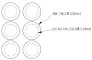
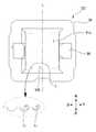
먼저 선행기술1을 참조하면, 지지부재에 형성된 개방 구멍은 반도체소자의 단자가 충분히 삽입될 수 있는 크기를 가져야 한다. 따라서 개방 구멍의 크기는 반도체소자의 단자가 가지는 크기의 최대 공차와 반도체소자의 단자 간의 간격 공차 및 반도체소자의 단자와 해당 접촉하는 소켓 간의 공차를 더한 최대 크기로 결정한다. 예를 들어, 반도체소자의 단자의 크기가 지름 0.23mm ±0.05mm(공차 부분)라고 하면 그 최대 크기는 지름 0.28mm가 된다. 여기에 반도체소자의 단자 간의 간격 공차와 반도체소자의 단자와 해당 단자에 접촉하는 소켓 간의 공차가 ±0.04mm이라고 하면, 개방 구멍의 크기는 0.32mm의 지름을 가지게 된다. 즉, 모든 공차들을 고려하였을 때, 개방 구멍의 크기가 0.32mm의 지름을 가져야만 반도체소자의 단자가 개방 구멍에 간섭 없이 출입할 수가 있는 것이다. 만일 모든 공차가 0.00mm인 최적의 조건에서는, 도 1에서 참조되는 바와 같이 반도체소자의 단자가 개방 구멍의 정 가운데 위치하는 것이 가장 바람직하다. 참고로, 도 1은 반도체소자를 인서트 하면에서 본 도면인데, 여기서 반도체소자를 일점쇄선으로 도시한 것은 개방 구멍과의 식별을 위한 것이다.First, referring to Prior Art 1, the open hole formed in the support member must have such a size that the terminals of the semiconductor element can be sufficiently inserted. Therefore, the size of the open hole is determined by the maximum size of the maximum tolerance of the size of the terminal of the semiconductor element plus the tolerance of the gap between the terminals of the semiconductor element and the tolerance between the terminal of the semiconductor element and the socket in contact therewith. For example, if the size of the terminal of the semiconductor element is 0.23 mm ± 0.05 mm (tolerance portion), the maximum size is 0.28 mm in diameter. Assuming that the tolerance between the terminals of the semiconductor elements and the tolerance between the terminals of the semiconductor element and the socket contacting the terminals are 0.04 mm, the size of the open hole has a diameter of 0.32 mm. That is, when all the tolerances are taken into account, the terminals of the semiconductor element can be inserted and removed without interfering with the open hole only if the size of the open hole is 0.32 mm in diameter. It is most preferable that the terminal of the semiconductor element is located in the center of the open hole, as shown in Fig. 1, under the optimal condition that all the tolerances are 0.00 mm. For reference, FIG. 1 is a view when a semiconductor device is viewed from an insert bottom. Here, the dotted line represents a semiconductor device for identification with an open hole.
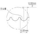
또한 도 2에서 참조되는 바와 같이, 선행기술2에서도 마찬가지로 안내홈의 곡률 반경이 0.32mm/2가 되어야 반도체소자의 단자가 적절히 안내홈에 의해 안내될 수 있게 되는 것이다.Also, as shown in Fig. 2, similarly to the
일반적으로, 반도체소자의 테스트에 있어서 가장 중요한 기술적 부분은 반도체소자와 테스터의 소켓 간의 전기적 접촉이다. 따라서 반도체소자의 단자의 위치는 테스터의 소켓의 위치와 정교히 대응될 필요성이 있으며, 이러한 필요성은 기술 발달에 따라 반도체소자의 단자 크기가 갈수록 작아짐에 따라 더욱 절실히 요구되고 있다.Generally, the most important technical part in testing semiconductor devices is the electrical contact between the semiconductor device and the socket of the tester. Therefore, the position of the terminal of the semiconductor element needs to correspond to the position of the socket of the tester, and this necessity is more urgently required as the size of the terminal of the semiconductor element becomes smaller as the technology is developed.
한편, 테스트핸들러에는 테스트트레이가 수직으로 세워진 상태에서 반도체소자의 테스트가 이루어지게 하는 수직식 테스트핸들러(사이드 도킹식 테스트핸들러라고 명명되기도 함)와 테스트트레이가 수평으로 세워진 상태에서 반도체소자의 테스트가 이루어지게 하는 수평식 테스트핸들러(언더헤드 도킹식 테스트핸들러라고 명명되기도 함)가 있다. 특히 수직식 테스트핸들러에서는 도 3에서 참조되는 바와 같이 테스트트레이가 수직으로 세워짐에 따라 인서트와 인서트에 안착된 반도체소자가 세워진 상태에서 테스트가 진행된다. 이러한 경우 도 4에서 참조되는 바와 같이 반도체소자는 자중에 의해 인서트의 안착 평면상에서 최대한 하측에 위치되기 마련이다. 따라서 수직식 테스트핸들러에서는 테스터의 소켓에 접촉될 반도체소자의 단자의 위치가 반도체소자의 하단을 기준으로 설정되게 인서트를 설계한다. 이 때, 수직으로 세워진 반도체소자의 하단은 안착 평면을 이루는 하단 턱에 접하기 때문에 반도체소자의 상하 방향으로의 위치가 정렬될 수 있다.On the other hand, the test handler includes a vertical type test handler (also called a side docking type test handler) that allows the semiconductor device to be tested with the test tray standing vertically, and a semiconductor device test (Sometimes referred to as an underhead docked test handler). In particular, in the vertical type test handler, as shown in FIG. 3, as the test tray is vertically erected, the test is carried out with the semiconductor element seated on the insert and the insert standing upright. In this case, as shown in Fig. 4, the semiconductor element is located at a maximum lower position on the seating plane of the insert due to its own weight. Therefore, in the vertical type test handler, the insert is designed such that the position of the terminal of the semiconductor element to be brought into contact with the socket of the tester is set with reference to the lower end of the semiconductor element. At this time, since the lower end of the vertically erected semiconductor element is in contact with the lower step that forms the seating plane, the position in the vertical direction of the semiconductor element can be aligned.
그런데, 단자에 대하여 안착 평면이 좌우 방향으로도 여유 간격이 있기 때문에 반도체소자가 안착 평면상에서 좌우 방향 중 일 측으로 치우칠 수 있다(도4에서는 좌측 방향으로 치우침). 이러한 경우 단자의 좌우 방향 위치가 테스터의 소켓과 일치하지 않게 되어 단자와 소켓간의 접촉이 불안정해 질 수 있다. 그래서 이를 해결하기 위한 본 발명의 출원인은 대한민국 특허 공개 10-2014-0057700호(발명의 명칭 : 테스트핸들러용 인서트, 이하 '선행기술3'이라 함)를 제안한 바 있다.However, since the seating plane has a clearance even in the left-right direction with respect to the terminal, the semiconductor element can be offset to one side in the lateral direction on the seating plane (in FIG. In this case, the position of the terminal in the left-right direction may not match the socket of the tester, and the contact between the terminal and the socket may become unstable. To solve this problem, the applicant of the present invention has proposed Korean Patent Laid-open Publication No. 10-2014-0057700 (entitled "Test Handler Insert", hereinafter referred to as "Prior Art 3").
위와 같은 선행기술3에 의하여 반도체소자의 상하 방향으로의 위치는 안착 평면을 이루는 하단 턱에 의해 정렬되고, 반도체소자의 좌우 방향으로의 위치는 특정 개방 구멍이나 특정 안내홈에 의해 정렬될 수 있어서 단자와 소켓 간의 전기적 접촉에 신뢰성이 향상될 수 있게 되었다.According to the prior art 3, the vertical position of the semiconductor element is aligned by the lower step constituting the seating plane, and the position of the semiconductor element in the left-right direction can be aligned by a specific opening or a specific guide groove, And the reliability of electrical contact between the socket and the socket can be improved.
그러나, 여전히 반도체의 집적도는 높아지면서, 그에 비례하여 반도체소자의 단자의 개수는 많아지고 그 크기는 작아지는 추세이며, 단자의 크기나 단자 간의 간격에 대한 공차는 줄어들 것이 요구되고 있다. 이에 따라 머지않아서 선행기술3에 의할 경우, 반도체소자의 하단이 안착 평면을 이루는 하단 턱에 접촉된 상태에서 단자가 특정 개방 구멍이나 안내홈에 강하게 끼이게 될 것이 예상된다. 만일 단자가 특정 개방 구멍이나 안내홈에 강하게 끼이고, 반도체소자의 하단까지 안착 평면을 이루는 하단 턱에 강하게 밀착되어서 끼이게 되면, 반도체소자를 인서트로부터 인출하는 과정에서 인출 불량이 이루어질 것이 예상된다(참고로, 반도체소자의 끼임이 문제되는 경우는 반도체소자가 수평으로 누운 상태이다. 여기 본 문장에서 '하단'은 설명의 편의를 위해서 반도체소자가 수직으로 세워진 상태의 방향을 기준으로 한 것이다). 즉, 진공 흡착에 의해 반도체소자를 인출할 때, 진공 흡착력이 반도체소자의 끼임 유지력에 미치지 못할 수 있게 되는 것이다.
However, as the degree of integration of semiconductors still increases, the number of terminals of the semiconductor elements increases and the size thereof becomes smaller in proportion thereto, and the tolerance on the size of the terminals and the interval between the terminals is required to be reduced. Accordingly, it is expected that in the case of the prior art 3, the terminal will be strongly caught in the specific opening hole or the guide groove in a state where the lower end of the semiconductor element is in contact with the lower end jaw forming the seating plane. If the terminal is strongly stuck in a specific opening or a guide groove and tightly adhered to the lower end of the semiconductor element to the lower end of the mounting surface, it is expected that the semiconductor element is pulled out from the insert For the sake of brevity, the semiconductor device is laid horizontally when there is a problem in the insertion of the semiconductor device. In this context, the 'bottom' is based on the direction in which the semiconductor device is vertically erected for convenience of explanation. That is, when the semiconductor element is pulled out by vacuum suction, the vacuum attraction force may not reach the holding force of the semiconductor element.
본 발명은 반도체소자의 단자가 가장 이상적인 위치에 놓이도록 안내할 수 있는 기능을 가지면서도 인서트에 안착된 반도체소자의 끼임 유지력을 최소화시킬 수 있는 기술을 제공하는 것이다.
The present invention provides a technique capable of minimizing the jam retention force of a semiconductor device mounted on an insert while having a function of guiding the terminal of the semiconductor device to be in the most ideal position.
위와 같은 목적을 달성하기 위한 본 발명의 제1 형태에 따른 테스트핸들러용 인서트는, 반도체소자가 삽입될 수 있는 삽입 구멍이 형성된 몸체; 상기 삽입 구멍의 일 측에서 상기 삽입 구멍에 삽입된 반도체소자를 지지하는 지지부재; 상기 지지부재를 상기 몸체에 고정시키는 고정부재; 및 상기 삽입 구멍 내에 반도체소자를 유지시키기 위한 래치장치; 를 포함하고, 상기 지지부재에 의해 지지된 반도체소자의 단자가 테스터 측에 전기적으로 연결될 수 있도록 상기 지지부재에는 반도체소자의 단자를 테스터 측으로 개방시키기 위한 개방 구멍들이 형성되어 있으며, 상기 개방 구멍들은 다수의 일반 개방 구멍과 적어도 2개의 특정 개방 구멍을 포함하고, 상기 적어도 2개의 특정 개방 구멍은 상기 다수의 일반 개방 구멍보다 반경이 작다.To achieve the above object, according to a first aspect of the present invention, there is provided an insert for a test handler, comprising: a body having an insertion hole into which a semiconductor device can be inserted; A supporting member for supporting the semiconductor element inserted into the insertion hole at one side of the insertion hole; A fixing member for fixing the supporting member to the body; And a latch device for holding the semiconductor element in the insertion hole; Wherein openings for opening the terminals of the semiconductor device to the tester side are formed in the support member such that terminals of the semiconductor device supported by the support member can be electrically connected to the tester side, And at least two specific openings, wherein the at least two specific openings are smaller in radius than the plurality of common openings.
상기 지지부재가 수직으로 세워졌음을 가정할 때, 상기 특정 개방 구멍의 중심을 지나가는 수직선과 상기 특정 개방 구멍의 중심을 지나가면서 상기 수직선에 직교하는 수평선을 그으면, 상기 수직선 또는 상기 수평선과 만나는 상기한 개방 구멍들의 중심은 상기 수직선 또는 상기 수평선상에 위치한다.The vertical line passing through the center of the specific opening hole and the horizontal line passing through the center of the specific opening hole and orthogonal to the vertical line are formed on the assumption that the support member is vertically erected, The centers of the open holes are located on the vertical line or the horizontal line.
상기 적어도 2개의 특정 개방 구멍에 대응되는 단자들이 상기 적어도 2개의 특정 개방 구멍에 삽입된 상태에 있는 반도체소자의 테두리단은 반도체소자가 안착되는 안착 평면을 이루는 사각 턱으로부터 이격되어 있다.
The edge portions of the semiconductor element in which the terminals corresponding to the at least two specific opening holes are inserted into the at least two specific opening holes are spaced apart from the square jaws forming the seating plane in which the semiconductor elements are seated.
또한, 위와 같은 목적을 달성하기 위한 본 발명의 제2 형태에 따른 테스트핸들러용 인서트는, 반도체소자가 삽입될 수 있는 삽입 구멍이 형성된 몸체; 및 상기 삽입 구멍 내에 반도체소자를 유지시키기 위한 래치장치; 를 포함하고, 상기 몸체는 상기 삽입 구멍의 하면을 이루는 사각 개방면에 상기 삽입 공간에 삽입된 반도체소자의 하방 이탈을 방지하기 위해 상호 맞은편 측으로 돌출된 이탈방지턱에 형성된 안내홈들을 가지며, 상기 안내홈들은 다수의 일반 안내홈과 적어도 2개의 특정 안내홈을 포함하고, 상기 적어도 2개의 특정 안내홈의 곡률 반경은 상기 다수의 일반 안내홈의 곡률 반경보다 작다.According to another aspect of the present invention, there is provided an insert for a test handler, including: a body having an insertion hole into which a semiconductor device can be inserted; And a latch device for holding the semiconductor element in the insertion hole; Wherein the body has guide grooves formed in a release protrusion protruding from opposite sides to prevent downward deviation of the semiconductor device inserted into the insertion space in a rectangular opening face constituting the lower surface of the insertion hole, The grooves include a plurality of general guide grooves and at least two specific guide grooves, and the radius of curvature of the at least two specific guide grooves is smaller than the radius of curvature of the plurality of general guide grooves.
상기 몸체가 수직으로 세워졌음을 가정할 때, 상기 특정 안내홈의 곡률 중심을 지나가는 수평선을 그으면, 상기 수평선과 만나는 상기한 안내홈들의 곡률 중심들은 상기 수평선상에 위치한다.Assuming that the body is vertically erected, the curvature centers of the guide grooves that meet the horizontal line are located on the horizontal line when passing a horizontal line passing through the center of curvature of the specific guide groove.
상기 적어도 2개의 특정 안내홈에 대응되는 단자들이 상기 적어도 2개의 안내홈에 삽입된 상태에 있는 반도체소자의 테두리단은 반도체소자가 안착되는 안착 평면을 이루는 사각 턱으로부터 이격되어 있다.
The edge of the semiconductor element in which the terminals corresponding to the at least two specific guide grooves are inserted into the at least two guide grooves is spaced apart from the square jaw forming the seating plane in which the semiconductor elements are seated.
본 발명에 따르면 다음과 같은 효과가 있다.The present invention has the following effects.
첫째, 특정 개방 구멍이나 안내홈만으로 반도체소자의 위치가 정확하게 설정될 수 있기 때문에 제품의 신뢰성을 향상시킬 수 있다.First, the reliability of the product can be improved because the position of the semiconductor element can be accurately set only by a specific opening hole or guide groove.
둘째, 안착 평면상에 있는 반도체소자의 하단이 안착 평면을 이루는 하단 턱과 이격되어 있어서 반도체소자의 끼임 유지력이 최소화되기 때문에 반도체소자의 인출 동작이 안정적으로 이루어질 수 있다.
Second, since the lower end of the semiconductor device on the seating plane is spaced apart from the lower end of the seating plane, the retracting operation of the semiconductor device can be stably performed because the clamping force of the semiconductor device is minimized.
도 1 내지 도 4는 배경기술의 설명에 참조하기 위한 참조도이다.
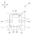
도 5는 본 발명의 실시예에 따른 테스트핸들러에 대한 개념적인 평면도이다.
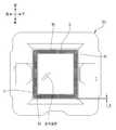
도 6은 본 발명의 제1 실시예에 따른 인서트에 대한 개략적인 평면도이다.
도 7 및 도 9는 도 6에 따른 인서트에서 특정 개방 구멍의 역할을 설명하기 위한 참조도이다.
도 10는 본 발명의 제2 실시예에 따른 인서트에 대한 개략적인 평면도이다.
도 11은 도9에 따른 인서트에서 특정 안내홈의 역할을 설명하기 위한 참조도이다.Figures 1 to 4 are reference diagrams for reference to the description of the background art.
5 is a conceptual top view of a test handler according to an embodiment of the present invention.
6 is a schematic plan view of an insert according to a first embodiment of the present invention.
Figs. 7 and 9 are reference views for explaining the role of the specific opening in the insert according to Fig.
10 is a schematic plan view of an insert according to a second embodiment of the present invention.
11 is a reference view for explaining the role of a specific guide groove in the insert according to FIG.
이하 상기한 바와 같은 본 발명에 따른 바람직한 실시예를 첨부된 도면을 참조하여 설명하되, 설명의 간결함을 위해 이미 주지되어 있는 기술이나 중복되는 설명은 가급적 생략하거나 압축한다.
DETAILED DESCRIPTION OF THE PREFERRED EMBODIMENTS Hereinafter, preferred embodiments of the present invention will be described with reference to the accompanying drawings, in which description or redundant description is omitted or compressed for simplicity of description.
<테스트핸들러><Test handler>
도 5는 본 발명의 실시예에 따른 테스트핸들러(500)에 대한 개략적인 평면 구성도이다.5 is a schematic plan view of a
도 5에서 참조되는 바와 같이 테스트핸들러(500)는 테스트트레이(510), 제1 핸드(520), 제1 로테이터(530), 테스트챔버(540), 제2 로테이터(550) 및 제2 핸드(560)를 포함한다.5, the
테스트트레이(510)에는 반도체소자가 안착될 수 있는 다수의 인서트들을 구비하고 있다. 이러한 테스트트레이(510)는 제1 위치(P1)에서 테스트위치(TP) 및 제2 위치(P2)를 거쳐 다시 제1 위치(P1)로 이어지는 폐쇄된 경로 C를 따라 순환한다. 여기서 인서트에 대해서는 별도의 목차로 나누어 후술한다.The
제1 핸드(520)는 제1 위치(LP1)에 위치된 테스트트레이(510)로 반도체소자를 로딩(loading)한다.The
제1 로테이터(530)는 반도체소자의 로딩이 완료된 테스트트레이(510)를 수직 상태로 회전시킨다.The
테스트챔버(540)는 테스트위치(TP)에 있는 수직 상태의 테스트트레이(510)에 적재된 반도체소자의 테스트를 위해 마련된다. 이를 위해 테스트챔버(540)의 내부는 반도체소자의 테스트 온도 조건에 따른 환경 상태로 유지된다.The
제2 로테이터(550)는 테스트챔버(540)로부터 온 수직 상태의 테스트트레이(510)를 수평 상태로 회전시킨다.The
제2 핸드(560)는 수평 상태로 제2 위치(P2)로 온 테스트트레이(510)로부터 반도체소자를 언로딩(unloading)시킨다.The
참고로, 테스트 온도 조건에 따라서 테스트트레이(510)는 폐쇄된 경로 C의 역방향으로 순환할 수 있다. 그리고 이 때에는 제1 핸드(520)와 제2 핸드의 역할과, 제1 로테이터(530)와 제2 로테이터(550)의 역할이 전환된다.
For reference, the
계속하여 상기한 바와 같은 테스트핸들러(500)에서 테스트트레이(510)에 구비되는 인서트의 예에 대하여 설명한다.
Next, an example of an insert included in the
<인서트에 대한 제1 실시예><First Embodiment of Insert>
도 6의 평면도를 참조하면, 제1 실시예에 따른 인서트(IS1)는 몸체(61), 지지부재(62) 및 래치장치(64)를 포함한다.6, the insert IS1 according to the first embodiment includes a
몸체(61)에는 반도체소자가 삽입될 수 있는 삽입 구멍(61a)이 형성되어 있다.The
지지부재(62)는 삽입 구멍(61a)의 하 측에서 삽입 구멍(61a)에 삽입된 반도체소자를 지지한다. 이러한 지지부재(62)에는 반도체소자의 단자를 테스터의 소켓 측으로 개방시키기 위한 다수의 개방 구멍(H)들이 반도체소자의 단자의 위치와 대응되는 위치에 형성되어 있다.The
한편, 개방 구멍(H)들 중 사각 귀퉁이 각각에 있는 소수의 특정 개방 구멍(H1)의 반경(r1)은 나머지 다수의 일반 개방 구멍(H0)의 반경(r0)보다 작은 정공(正孔)이다. 그리고 특정 개방 구멍(H1)들의 개수는 일반 개방 구멍(H0)들의 개수보다 상당히 적어야 한다.The radius r1 of the small number of specific openings H1 in each of the square corners of the open holes H is smaller than the radius r0 of the remaining large openings H0 Hole). And the number of specific opening holes H1 should be considerably smaller than the number of general opening holes H0 .
특정 개방 구멍(H1)은 반도체소자의 위치를 정확하게 설정할 목적으로 구성되었다. 따라서 특정 개방 구멍(H1)의 반경(r1)은 반도체소자의 단자의 이상적인 반경과 동일한 정도의 크기를 가지는 것이 바람직하며, 이로 인해 단자가 특정 개방 구멍(H1)에 끼이는 현상도 발생할 수 있음을 충분히 고려하였다. 이러한 특정 개방 구멍(H1)은 적어도 2개 이상 형성될 수 있다. 그리고 적어도 2개 이상의 특정 개방 구멍(H1)들은 지지부재(62)가 수직으로 세워졌을 때 반도체소자의 양단의 높이가 동일할 수 있도록 지지부재(62)를 절반으로 나누는 직선(L)상에서 양 측으로 나누어 배치되는 것이 바람직하다.The specific opening H1 is configured for precisely setting the position of the semiconductor element. Therefore, it is preferable that the radius r1 of the specific opening H1 has a size approximately equal to the ideal radius of the terminal of the semiconductor element, thereby causing the phenomenon that the terminal is caught in the specific opening H1 . At least two or more of these specific opening holes H1 may be formed. At least two or more specific openings H1 are formed on the straight line L dividing the
일반 개방 구멍(H0)들은 배경기술에서 언급한 여러 제작 공차들을 감안하더라도 대응하는 단자가 넉넉히 삽입될 수 있는 크기의 반경을 가지는 정공으로 형성된다. 이로 인해 반도체소자의 단자가 일반 개방 구멍에 끼이는 현상이 방지될 수 있다.The general open holes H0 are formed into holes having a radius of a size enough to allow a corresponding terminal to be inserted even when considering various manufacturing tolerances mentioned in the background art. This can prevent the terminal of the semiconductor element from being caught in the normal opening.
더 구체적인 예를 들어 도 7에서와 같이 반도체소자의 단자가 0.24mm의 직경을 가진다면, 지지부재(62)의 특정 개방구멍(H1)은 직경이 0.27mm로써 0.03mm 정도의 공차 수준을 가지게 형성한다. 만일 특정 개방구멍(H1)의 직경이 단자의 직경과 동일하다면, 단자가 특정 개방구멍(H1)에 끼임으로 인해 단자를 특정 개방구멍(H1)으로부터 분리하는 것이 곤란해질 수 있기 때문에, 특정 개방구멍(H1)의 수가 현격히 제한 받게 된다. 따라서 0.03mm 정도의 공차 수준을 고려하여 특정 개방구멍(H1)의 직경을 결정하면, 지지부재(62)의 사각 귀퉁이에 5개씩의 특정 개방 구멍(H1)을 형성하는 것이 반도체소자를 정확하고 안정적으로 지지함으로써 반도소자의 단자와 테스트소켓 간의 정확한 전기적 접촉을 가능하게 하고, 추후 지지부재(62)로부터 반도체소자의 단자를 분리시킬 때도 단자의 손상 없이 분리가 가능함을 무수한 반복 실험을 통해 알게 되었다. 그리고 일반 개방구멍(H0)의 경우에는 단자 크기의 공차 ±0.05mm와 단자의 변위 공차 ±0.03mm이므로, 일반 개방구멍(H0)의 직경을 0.32mm로 설계한다.7, if the terminal of the semiconductor device has a diameter of 0.24 mm, the specific opening H1 of the
한편, 도 8a에서와 같이 지지부재(62)가 수직으로 세워졌을 때, 특정 개방 구멍(H1)의 중심(O1)을 지나가는 수직선(P)과 특정 개방 구멍(H1)의 중심(O1)을 지나가면서 수직선(P)에 직교하는 수평선(H)을 그으면, 수직선(P) 또는 수평선(H)과 만나는 개방 구멍(H)들(H1, H0) 각각의 중심(O1, O0)은 수직선(P) 또는 수평선(H)상에 위치함으로써 반도체소자에 구비된 단자들의 이상적인 중심이 개방 구멍(H)들의 중심과 일치될 수 있어야 한다.On the other hand, even when the
래치장치(64)는 삽입 구멍(61a) 내에 반도체소자를 유지시킨다.The
위와 같은 구성의 인서트(IS1)에서 반도체소자가 인서트(IS1)에 적재되면, 도 8b에서와 같이 지지부재(62)가 수직으로 세워졌을 때, 반도체소자의 단자(T)가 특정 개방 구멍(H1)에 삽입된 상태에서 단자(T)의 하단이 특정 개방구멍(H1)의 하단에 접함으로써 반도체소자의 위치가 설정되기 때문에 테스트트레이(510)의 흔들림이나 이동 중에 충격이 발생하더라도 적어도 테스트 시에는 반도체소자의 위치가 정교하게 설정될 수 있게 된다. 이로 인해 반도체소자의 단자(T)와 테스트소켓 간의 정교한 접촉이 담보된다. 그리고 이 때, 일반 개방구멍(H0)에 삽입된 단자는 접촉 부분이 없는 들뜬 상태로 있게 된다. 물론, 지지부재(62)가 수직으로 세워진 상태이기 때문에 단자(T)와 일반 개방구멍(H0)의 하단의 이격 거리(d1)는 단자(T)와 일반 개방구멍(H0)의 상단의 이격 거리(d2)보다 다소 작다. 따라서 특정 개방구멍(H1)의 직경은 반도체소자의 단자의 직경보다는 크지만, 일반 개방구멍(H0)의 직경보다는 작으면서 인서트(IS1)가 수직으로 세워졌을 때 일반 개방구멍(H0)에 대응되는 단자(T)가 끼임 없이 들 뜬 상태를 유지할 수 있는 크기인 것이 바람직하다.When the semiconductor element is loaded on the insert IS1 in the above-described configuration IS1, when the
한편, 도 9에서와 같이 테스트트레이(510)가 수직 상태로 세워짐으로써 인서트(IS1) 및 반도체소자(D)가 수직으로 세워진 상태를 기준으로, 반도체소자(D)의 하단이 안착 평면을 이루는 하단 턱(BJ)과 소정 간격(A) 이격되는 것이 더욱 바람직하다. 왜냐하면, 인서트(IS1)가 수직으로 세워진 상태에서, 인서트(IS1)의 안착 평면을 이루는 하단 턱(BJ)과 반도체소자(D)의 하단이 접촉함으로써 반도체소자의 위치가 설정되도록 하면, 특정 개방구멍(H1)에 대응되는 단자가 특정 개방구멍(H1)의 위치를 벗어나거나 또는 살짝 걸쳐진 상태에서 단자(T)와 테스트소켓 간의 접촉에 필요한 압력이 가해질 수 있다. 이러한 경우 단자(T)나 지지부재(62)가 상호 파손되거나, 특정 개방구멍(H0)에 단자가 꽉 끼이게 되고, 반도체소자(D)의 하단마저 안착 평면을 이루는 하단 턱(BJ)에 강하게 끼일 수 있기 때문에 추후 지지부재(62)로부터 단자를 분리하는 작업에 문제가 발생할 수 있다. 따라서 인서트(IS1) 및 반도체소자(D)가 수직으로 세워진 상태에서, 반도체소자(D)의 하단이 안착 평면을 이루는 하단 턱(BJ)과 소정 간격(A) 이격되도록 함으로써 반도체소자(D)의 하단이 하단 턱(BJ)에 끼이는 현상을 방지시킨다. 즉, 본 발명의 가장 바람직한 예에서는 반도체소자가 수직으로 세워졌을 때, 반도체소자가 특정 개방구멍(H1)에 대응되는 단자들을 통해서 지지부재(62)에 의해서만 지지된다. 물론, 반도체소자(D)의 나머지 테두리단도 안착 평면을 이루는 나머지 턱들(LJ, TJ, RJ)로부터 모두 이격되어 있는 것이 바람직하다. 즉, 안착 평면을 이루는 사각 턱(LJ, TJ, RJ, BJ)과 안착 평면에 놓인 반도체소자(D)의 테두리단은 모두 이격되는 것이 바람직하다. 이로 인해 반도체소자(D)는 특정 개방 구멍(H1)들에 삽입되는 단자(T)들 외에는 인서트(IS1) 측과 끼움 간섭이 발생되지 않는다. 그리고 이러한 점은 인서트(IS1)와의 끼임 간섭에 따른 반도체소자(D)의 끼임 유지력을 최소화시키기 때문에, 제1 핸드(520) 또는 제2 핸드(560)에 의해 반도체소자(D)를 인서트(IS1)로부터 언로딩시킬 때 제1 핸드(520)나 제2 핸드(560)에 의한 반도체소자(D)의 흡착력이 반도체소자(D)의 끼임 유지력보다 클 수 있는 조건을 가지게 한다. 이로 인해 제1 핸드(520)나 제2 핸드(560)에 의한 반도체소자(D)의 언로딩 작업이 적절히 이루어질 수 있다.
9, the
<인서트에 대한 제2 예>≪ Second Example of Insert >
도 10의 평면도를 참조하면, 제2 실시예에 따른 인서트(IS2)는 몸체(91) 및 래치장치(94)를 포함한다.10, the insert IS2 according to the second embodiment includes a
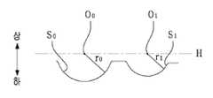
몸체(91)에는 반도체소자가 삽입될 수 있는 삽입 구멍(91a)이 형성되어 있다. 또한 몸체(91)는 삽입 구멍(91a)의 하면을 이루는 사각 개방면에 삽입 구멍(91a)에 삽입된 반도체소자의 하방 이탈을 방지하기 위해 수평 방향의 맞은편 측으로 돌출된 이탈방지턱(91b)을 가진다. 그리고 이탈방지턱(91b)에는 반도체소자의 단자를 안내하기 위한 안내홈(S)들이 형성되어 있다.The
안내홈(S)들 중 상대적으로 소수인 특정 안내홈(S1)들의 곡률 반경(r1)은 상대적으로 다수인 나머지 일반 안내홈(S0)들의 곡률 반경(r2)보다 작다. 특정 안내홈(S1)은 반도체소자의 위치를 정확하게 설정할 목적으로 구성되었다. 따라서 특정 안내홈(S1)의 곡률 반경(r1)은 반도체소자의 단자의 이상적인 반경과 동일한 정도의 크기를 가지는 것이 바람직하며, 이로 인해 단자가 특정 안내홈(S1)에 끼이는 현상도 발생할 수 있음을 충분히 고려하였다. 이러한 특정 안내홈(S1)은 적어도 2개 이상 형성될 수 있다. 그리고 적어도 2개 이상의 특정 안내홈(S1)들은 몸체(91)를 절반으로 나누는 직선(L)상에서 양 측으로 나누어 배치되는 것이 바람직하다.The curvature radius r1 of the specific guide grooves S1 which are a relatively small number of the guide grooves S is smaller than the curvature radius r2 of the remaining general guide grooves S0 which are relatively large. The specific guide groove S1 is configured for precisely setting the position of the semiconductor element. Therefore, it is preferable that the radius of curvature r1 of the specific guide groove S1 has a size approximately equal to the ideal radius of the terminal of the semiconductor element, and consequently the phenomenon that the terminal is caught in the specific guide groove S1 It is possible that the This particular guide grooves (S1) can be formed of at least two. It is preferable that at least two specific guide grooves S1 are arranged on both sides on a straight line L dividing the
일반 안내홈(S0)들은 배경기술에서 언급한 여러 제작 공차들을 감안하더라도 대응하는 단자가 넉넉히 삽입될 수 있는 크기의 곡률 반경(r0)을 가지도록 형성된다. 이로 인해 반도체소자의 단자가 일반 안내홈(S0)에 끼이는 현상이 방지될 수 있다.
The general guide grooves S0 are formed so as to have a radius of curvature r0 of such a size that a corresponding terminal can be inserted more even when considering various manufacturing tolerances mentioned in the background art. This can prevent the terminals of the semiconductor element from being caught in the general guide groove S0 .
또한, 도 11에서 참조되는 바와 같이 몸체(91)가 수직으로 세워졌을 때, 특정 안내홈(S1)의 곡률 중심(O1)을 지나가는 수평선(H)을 그으면, 수평선(H)과 만나는 안내홈(S)들의 곡률 중심(O1, O0)들은 수평선(H)상에 위치함으로써 반도체소자에 구비된 단자들의 이상적인 중심이 안내홈(S)들의 곡률 중심(O1, O0)과 일치될 수 있어야 한다.11, when the
래치장치(94)는 삽입 구멍(91a) 내에 반도체소자를 유지시킨다.The
물론, 본 실시예에서도 인서트(IS2)에 적재된 반도체소자(D)의 테두리단은 안착 평면을 이루는 사각 턱으로부터 모두 이격되도록 안내홈(S)들이 형성되는 것이 바람직하다.
Of course, also in this embodiment, it is preferable that the edge of the semiconductor element D mounted on the insert IS2 is formed with the guide grooves S so as to be spaced apart from the square jaws forming the seating plane.
위에서 설명된 실시예들은 수직식 테스트핸들러를 예로 들어 설명하고 있지만, 본 발명은 수평식 테스트핸들러에서도 얼마든지 적용될 수 있다.
While the embodiments described above illustrate vertical test handlers as an example, the present invention can be applied to any number of horizontal test handlers.
상술한 바와 같이, 본 발명에 대한 구체적인 설명은 첨부된 도면을 참조한 실시예에 의해서 이루어졌지만, 상술한 실시예는 본 발명의 바람직한 예를 들어 설명하였을 뿐이기 때문에, 본 발명이 상기의 실시예에만 국한되는 것으로 이해되어져서는 아니 되며, 본 발명의 권리범위는 후술하는 청구범위 및 그 등가개념으로 이해되어져야 할 것이다.
Although the present invention has been fully described by way of example only with reference to the accompanying drawings, it is to be understood that the present invention is not limited thereto. It is to be understood that the scope of the invention is to be construed as being limited only by the following claims and their equivalents.
IS1, IS2 : 인서트
61, 91 : 몸체
61a, 91a : 삽입 구멍
91b : 이탈방지턱
S : 안내홈
S0 : 일반 안내홈
S1 : 특정 안내홈
62 : 지지부재
H : 개방 구멍
H0 : 일반 개방 구멍
H1 : 특정 개방 구멍
64, 94 : 래치장치IS1, IS2: Insert
61, 91: Body
61a, 91a: insertion hole
91b:
S: guide home
S0 : General guide home
S1 : Specific guide home
62: Support member
H: opening hole
H0 : Normal open hole
H1 : Specific opening hole
64, 94: latch device
Claims (6)
Translated fromKorean상기 삽입 구멍의 일 측에서 상기 삽입 구멍에 삽입된 반도체소자를 지지하는 지지부재;
상기 지지부재를 상기 몸체에 고정시키는 고정부재; 및
상기 삽입 구멍 내에 반도체소자를 유지시키기 위한 래치장치; 를 포함하고,
상기 지지부재에 의해 지지된 반도체소자의 단자가 테스터 측에 전기적으로 연결될 수 있도록 상기 지지부재에는 반도체소자의 단자를 테스터 측으로 개방시키기 위한 개방 구멍들이 형성되어 있으며,
상기 개방 구멍들은 다수의 일반 개방 구멍과 적어도 2개의 특정 개방 구멍을 포함하고,
상기 적어도 2개의 특정 개방 구멍은 상기 다수의 일반 개방 구멍보다 반경이 작은 것을 특징으로 하는
테스트핸들러용 인서트.A body having an insertion hole into which a semiconductor device can be inserted;
A supporting member for supporting the semiconductor element inserted into the insertion hole at one side of the insertion hole;
A fixing member for fixing the supporting member to the body; And
A latch device for holding the semiconductor element in the insertion hole; Lt; / RTI >
Wherein the support member is formed with open holes for opening the terminal of the semiconductor element to the tester side so that the terminal of the semiconductor element supported by the support member can be electrically connected to the tester side,
Wherein the open holes include a plurality of general open holes and at least two specific open holes,
Characterized in that the at least two specific opening holes are smaller in radius than the plurality of general opening holes
Insert for test handler.
상기 지지부재가 수직으로 세워졌음을 가정할 때, 상기 특정 개방 구멍의 중심을 지나가는 수직선과 상기 특정 개방 구멍의 중심을 지나가면서 상기 수직선에 직교하는 수평선을 그으면, 상기 수직선 또는 상기 수평선과 만나는 상기한 개방 구멍들의 중심은 상기 수직선 또는 상기 수평선상에 위치하는 것을 특징으로 하는
테스트핸들러용 인서트.The method according to claim 1,
The vertical line passing through the center of the specific opening hole and the horizontal line passing through the center of the specific opening hole and orthogonal to the vertical line are formed on the assumption that the support member is vertically erected, And the centers of the open holes are located on the vertical line or the horizontal line.
Insert for test handler.
상기 적어도 2개의 특정 개방 구멍에 대응되는 단자들이 상기 적어도 2개의 특정 개방 구멍에 삽입된 상태에 있는 반도체소자의 테두리단은 반도체소자가 안착되는 안착 평면을 이루는 사각 턱으로부터 이격된 것을 특징으로 하는
테스트핸들러용 인서트.The method according to claim 1,
Wherein edge portions of the semiconductor element in which the terminals corresponding to the at least two specific opening holes are inserted into the at least two specific opening holes are spaced apart from a square jaw forming a seating plane in which the semiconductor elements are seated
Insert for test handler.
상기 삽입 구멍 내에 반도체소자를 유지시키기 위한 래치장치; 를 포함하고,
상기 몸체는 상기 삽입 구멍의 하면을 이루는 사각 개방면에 상기 삽입 공간에 삽입된 반도체소자의 하방 이탈을 방지하기 위해 상호 맞은편 측으로 돌출된 이탈방지턱에 형성된 안내홈들을 가지며,
상기 안내홈들은 다수의 일반 안내홈과 적어도 2개의 특정 안내홈을 포함하고,
상기 적어도 2개의 특정 안내홈의 곡률 반경은 상기 다수의 일반 안내홈의 곡률 반경보다 작은 것을 특징으로 하는
테스트핸들러용 인서트.A body having an insertion hole into which a semiconductor device can be inserted; And
A latch device for holding the semiconductor element in the insertion hole; Lt; / RTI >
Wherein the body has guide grooves formed in a separation protrusion protruded from opposite sides to prevent downward departure of the semiconductor device inserted into the insertion space in a square opening face constituting the lower surface of the insertion hole,
Wherein the guide grooves include a plurality of general guide grooves and at least two specific guide grooves,
Wherein a radius of curvature of the at least two specific guide grooves is smaller than a radius of curvature of the plurality of general guide grooves
Insert for test handler.
상기 몸체가 수직으로 세워졌음을 가정할 때, 상기 특정 안내홈의 곡률 중심을 지나가는 수평선을 그으면, 상기 수평선과 만나는 상기한 안내홈들의 곡률 중심들은 상기 수평선상에 위치하는 것을 특징으로 하는
테스트핸들러용 인서트.5. The method of claim 4,
The center of curvature of the guide grooves meeting the horizontal line is located on the horizontal line when the horizontal line passes through the center of curvature of the specific guide groove assuming that the body is vertically erected.
Insert for test handler.
상기 적어도 2개의 특정 안내홈에 대응되는 단자들이 상기 적어도 2개의 안내홈에 삽입된 상태에 있는 반도체소자의 테두리단은 반도체소자가 안착되는 안착 평면을 이루는 사각 턱으로부터 이격된 것을 특징으로 하는
테스트핸들러용 인서트.
6. The method of claim 5,
Wherein the edge of the semiconductor element in which the terminals corresponding to the at least two specific guide grooves are inserted into the at least two guide grooves is spaced apart from a square jaw forming a seating plane on which the semiconductor elements are seated,
Insert for test handler.
Priority Applications (4)
| Application Number | Priority Date | Filing Date | Title |
|---|---|---|---|
| KR1020150062674AKR102252638B1 (en) | 2015-05-04 | 2015-05-04 | Insert for test handler |
| JP2016088113AJP6111362B2 (en) | 2015-05-04 | 2016-04-26 | Insert for test handler |
| CN201610290830.1ACN106111552B (en) | 2015-05-04 | 2016-05-04 | Testing, sorting machine plug connector |
| KR1020210056744AKR102364598B1 (en) | 2015-05-04 | 2021-04-30 | Insert for test handler |
Applications Claiming Priority (1)
| Application Number | Priority Date | Filing Date | Title |
|---|---|---|---|
| KR1020150062674AKR102252638B1 (en) | 2015-05-04 | 2015-05-04 | Insert for test handler |
Related Child Applications (1)
| Application Number | Title | Priority Date | Filing Date |
|---|---|---|---|
| KR1020210056744ADivisionKR102364598B1 (en) | 2015-05-04 | 2021-04-30 | Insert for test handler |
Publications (2)
| Publication Number | Publication Date |
|---|---|
| KR20160130643Atrue KR20160130643A (en) | 2016-11-14 |
| KR102252638B1 KR102252638B1 (en) | 2021-05-17 |
Family
ID=57269865
Family Applications (2)
| Application Number | Title | Priority Date | Filing Date |
|---|---|---|---|
| KR1020150062674AActiveKR102252638B1 (en) | 2015-05-04 | 2015-05-04 | Insert for test handler |
| KR1020210056744AActiveKR102364598B1 (en) | 2015-05-04 | 2021-04-30 | Insert for test handler |
Family Applications After (1)
| Application Number | Title | Priority Date | Filing Date |
|---|---|---|---|
| KR1020210056744AActiveKR102364598B1 (en) | 2015-05-04 | 2021-04-30 | Insert for test handler |
Country Status (3)
| Country | Link |
|---|---|
| JP (1) | JP6111362B2 (en) |
| KR (2) | KR102252638B1 (en) |
| CN (1) | CN106111552B (en) |
Citations (4)
| Publication number | Priority date | Publication date | Assignee | Title |
|---|---|---|---|---|
| KR20090020298A (en)* | 2007-08-23 | 2009-02-26 | 파워테크 테크놀로지 인코포레이티드 | Universal insert tool for securing BA packages during testing |
| JP2009204619A (en)* | 2004-07-28 | 2009-09-10 | Fujitsu Ltd | Substrate unit and printed circuit board |
| KR20140057700A (en)* | 2012-10-26 | 2014-05-14 | (주)테크윙 | Insert for test handler |
| KR20150035347A (en)* | 2013-09-27 | 2015-04-06 | 세메스 주식회사 | Insert assembly of test tray |
Family Cites Families (13)
| Publication number | Priority date | Publication date | Assignee | Title |
|---|---|---|---|---|
| TW369692B (en)* | 1997-12-26 | 1999-09-11 | Samsung Electronics Co Ltd | Test and burn-in apparatus, in-line system using the apparatus, and test method using the system |
| KR100800312B1 (en)* | 2006-01-25 | 2008-02-04 | (주)테크윙 | Test handler and loading method of test handler |
| KR100687676B1 (en)* | 2006-02-10 | 2007-02-27 | (주)테크윙 | Test handler |
| KR200427177Y1 (en) | 2006-07-06 | 2006-09-20 | 주식회사 오킨스전자 | Semiconductor Chip Carrier |
| JP5022381B2 (en)* | 2006-12-21 | 2012-09-12 | 株式会社アドバンテスト | Electronic component testing apparatus and electronic component testing method |
| CN101758031B (en)* | 2010-03-02 | 2014-03-05 | 王晓军 | Integrated circuit testing and sorting method and device thereof |
| KR101658078B1 (en)* | 2012-01-03 | 2016-09-21 | (주)테크윙 | Test handler |
| CN103302037B (en)* | 2012-03-16 | 2016-01-13 | 泰克元有限公司 | test sorter |
| KR101334765B1 (en)* | 2012-04-18 | 2013-11-29 | 미래산업 주식회사 | Handling System for Semiconductor device |
| KR101706982B1 (en)* | 2012-08-16 | 2017-02-16 | (주)테크윙 | Insert for test handler |
| KR101715827B1 (en)* | 2012-09-27 | 2017-03-14 | (주)테크윙 | Insert for test handler |
| KR102010916B1 (en)* | 2013-05-14 | 2019-08-14 | 삼성전자주식회사 | Semiconductor package testing structure |
| KR101968985B1 (en)* | 2018-12-19 | 2019-08-26 | (주)테크윙 | Insert for test handler |
- 2015
- 2015-05-04KRKR1020150062674Apatent/KR102252638B1/enactiveActive
- 2016
- 2016-04-26JPJP2016088113Apatent/JP6111362B2/enactiveActive
- 2016-05-04CNCN201610290830.1Apatent/CN106111552B/enactiveActive
- 2021
- 2021-04-30KRKR1020210056744Apatent/KR102364598B1/enactiveActive
Patent Citations (4)
| Publication number | Priority date | Publication date | Assignee | Title |
|---|---|---|---|---|
| JP2009204619A (en)* | 2004-07-28 | 2009-09-10 | Fujitsu Ltd | Substrate unit and printed circuit board |
| KR20090020298A (en)* | 2007-08-23 | 2009-02-26 | 파워테크 테크놀로지 인코포레이티드 | Universal insert tool for securing BA packages during testing |
| KR20140057700A (en)* | 2012-10-26 | 2014-05-14 | (주)테크윙 | Insert for test handler |
| KR20150035347A (en)* | 2013-09-27 | 2015-04-06 | 세메스 주식회사 | Insert assembly of test tray |
Also Published As
| Publication number | Publication date |
|---|---|
| CN106111552B (en) | 2018-11-16 |
| JP6111362B2 (en) | 2017-04-05 |
| KR20210055646A (en) | 2021-05-17 |
| CN106111552A (en) | 2016-11-16 |
| JP2016212099A (en) | 2016-12-15 |
| KR102364598B1 (en) | 2022-02-23 |
| KR102252638B1 (en) | 2021-05-17 |
Similar Documents
| Publication | Publication Date | Title |
|---|---|---|
| CN114731768B (en) | Semiconductor test socket having latch and floating plate for holding semiconductor device | |
| JP5456345B2 (en) | Test tray insert opening unit and semiconductor element mounting method using the same | |
| KR20120138517A (en) | Apparatus for fastening chip and testing method using them | |
| TW201632889A (en) | Test device | |
| KR102637464B1 (en) | Apparatus for opening latches of insert assemblies | |
| KR101955194B1 (en) | Insert for test handler | |
| KR102490589B1 (en) | Insert assembly for receiving electronic device, test tray including the insert assembly and apparatus for opening latch of the insert assembly | |
| KR20160130643A (en) | Insert for test handler | |
| KR101715827B1 (en) | Insert for test handler | |
| KR102220334B1 (en) | Insert assembly for receiving electronic device | |
| KR102471835B1 (en) | Insert for test handler | |
| KR20190003431A (en) | Insert for test handler | |
| KR20190024925A (en) | Insert for test handler | |
| US11525859B2 (en) | Insertion/extraction mechanism and method for replacing block member | |
| TWI604207B (en) | Insert for test handler | |
| CN106994445B (en) | Test sorting machine | |
| KR101600272B1 (en) | Pushing unit of match plate and match plate for test handler and test handler | |
| KR100465372B1 (en) | Carrier Module for Semiconductor Test Handler | |
| TWI737967B (en) | Chip carrier | |
| TWI734002B (en) | Carrier for electronic component testing device | |
| KR102470315B1 (en) | Insert for test handler | |
| KR20160136526A (en) | Insert assembly for receiving electronic device, test tray including the insert assembly and apparatus for opening latch of the insert assembly | |
| KR101652901B1 (en) | Side docking type test handler and pushing apparatus for test handler | |
| KR101494176B1 (en) | Test system of semiconductor device | |
| KR20180001922A (en) | Method of sorting wafers stored in cassette |
Legal Events
| Date | Code | Title | Description |
|---|---|---|---|
| PA0109 | Patent application | Patent event code:PA01091R01D Comment text:Patent Application Patent event date:20150504 | |
| PG1501 | Laying open of application | ||
| PA0201 | Request for examination | Patent event code:PA02012R01D Patent event date:20200114 Comment text:Request for Examination of Application Patent event code:PA02011R01I Patent event date:20150504 Comment text:Patent Application | |
| E902 | Notification of reason for refusal | ||
| PE0902 | Notice of grounds for rejection | Comment text:Notification of reason for refusal Patent event date:20201210 Patent event code:PE09021S01D | |
| E701 | Decision to grant or registration of patent right | ||
| PE0701 | Decision of registration | Patent event code:PE07011S01D Comment text:Decision to Grant Registration Patent event date:20210215 | |
| PA0107 | Divisional application | Comment text:Divisional Application of Patent Patent event date:20210430 Patent event code:PA01071R01D | |
| GRNT | Written decision to grant | ||
| PR0701 | Registration of establishment | Comment text:Registration of Establishment Patent event date:20210511 Patent event code:PR07011E01D | |
| PR1002 | Payment of registration fee | Payment date:20210512 End annual number:3 Start annual number:1 | |
| PG1601 | Publication of registration | ||
| PR1001 | Payment of annual fee | Payment date:20240508 Start annual number:4 End annual number:4 | |
| PR1001 | Payment of annual fee | Payment date:20250415 Start annual number:5 End annual number:5 |