KR20160124992A - apparatus for manufacturing a substrate and ceramic film coating method of the same - Google Patents
apparatus for manufacturing a substrate and ceramic film coating method of the sameDownload PDFInfo
- Publication number
- KR20160124992A KR20160124992AKR1020150055418AKR20150055418AKR20160124992AKR 20160124992 AKR20160124992 AKR 20160124992AKR 1020150055418 AKR1020150055418 AKR 1020150055418AKR 20150055418 AKR20150055418 AKR 20150055418AKR 20160124992 AKR20160124992 AKR 20160124992A
- Authority
- KR
- South Korea
- Prior art keywords
- buffer layer
- thin film
- ceramic thin
- yttrium
- film
- Prior art date
- Legal status (The legal status is an assumption and is not a legal conclusion. Google has not performed a legal analysis and makes no representation as to the accuracy of the status listed.)
- Withdrawn
Links
Images


Classifications
- H—ELECTRICITY
- H01—ELECTRIC ELEMENTS
- H01J—ELECTRIC DISCHARGE TUBES OR DISCHARGE LAMPS
- H01J37/00—Discharge tubes with provision for introducing objects or material to be exposed to the discharge, e.g. for the purpose of examination or processing thereof
- H01J37/32—Gas-filled discharge tubes
- H01J37/32431—Constructional details of the reactor
- H01J37/32458—Vessel
- H01J37/32477—Vessel characterised by the means for protecting vessels or internal parts, e.g. coatings
- H01J37/32495—Means for protecting the vessel against plasma
- H—ELECTRICITY
- H01—ELECTRIC ELEMENTS
- H01L—SEMICONDUCTOR DEVICES NOT COVERED BY CLASS H10
- H01L21/00—Processes or apparatus adapted for the manufacture or treatment of semiconductor or solid state devices or of parts thereof
- H01L21/02—Manufacture or treatment of semiconductor devices or of parts thereof
- H01L21/04—Manufacture or treatment of semiconductor devices or of parts thereof the devices having potential barriers, e.g. a PN junction, depletion layer or carrier concentration layer
- H01L21/48—Manufacture or treatment of parts, e.g. containers, prior to assembly of the devices, using processes not provided for in a single one of the groups H01L21/18 - H01L21/326 or H10D48/04 - H10D48/07
- H01L21/4803—Insulating or insulated parts, e.g. mountings, containers, diamond heatsinks
- H01L21/4807—Ceramic parts
- H—ELECTRICITY
- H01—ELECTRIC ELEMENTS
- H01J—ELECTRIC DISCHARGE TUBES OR DISCHARGE LAMPS
- H01J37/00—Discharge tubes with provision for introducing objects or material to be exposed to the discharge, e.g. for the purpose of examination or processing thereof
- H01J37/32—Gas-filled discharge tubes
- H01J37/32009—Arrangements for generation of plasma specially adapted for examination or treatment of objects, e.g. plasma sources
- H01J37/32082—Radio frequency generated discharge
- H01J37/321—Radio frequency generated discharge the radio frequency energy being inductively coupled to the plasma
- H—ELECTRICITY
- H01—ELECTRIC ELEMENTS
- H01J—ELECTRIC DISCHARGE TUBES OR DISCHARGE LAMPS
- H01J37/00—Discharge tubes with provision for introducing objects or material to be exposed to the discharge, e.g. for the purpose of examination or processing thereof
- H01J37/32—Gas-filled discharge tubes
- H01J37/32431—Constructional details of the reactor
- H01J37/32458—Vessel
- H01J37/32477—Vessel characterised by the means for protecting vessels or internal parts, e.g. coatings
- H—ELECTRICITY
- H01—ELECTRIC ELEMENTS
- H01L—SEMICONDUCTOR DEVICES NOT COVERED BY CLASS H10
- H01L21/00—Processes or apparatus adapted for the manufacture or treatment of semiconductor or solid state devices or of parts thereof
- H01L21/02—Manufacture or treatment of semiconductor devices or of parts thereof
- H01L21/02104—Forming layers
- H01L21/02107—Forming insulating materials on a substrate
- H01L21/02109—Forming insulating materials on a substrate characterised by the type of layer, e.g. type of material, porous/non-porous, pre-cursors, mixtures or laminates
- H01L21/02112—Forming insulating materials on a substrate characterised by the type of layer, e.g. type of material, porous/non-porous, pre-cursors, mixtures or laminates characterised by the material of the layer
- H01L21/02123—Forming insulating materials on a substrate characterised by the type of layer, e.g. type of material, porous/non-porous, pre-cursors, mixtures or laminates characterised by the material of the layer the material containing silicon
- H01L21/02126—Forming insulating materials on a substrate characterised by the type of layer, e.g. type of material, porous/non-porous, pre-cursors, mixtures or laminates characterised by the material of the layer the material containing silicon the material containing Si, O, and at least one of H, N, C, F, or other non-metal elements, e.g. SiOC, SiOC:H or SiONC
- H01L21/02131—Forming insulating materials on a substrate characterised by the type of layer, e.g. type of material, porous/non-porous, pre-cursors, mixtures or laminates characterised by the material of the layer the material containing silicon the material containing Si, O, and at least one of H, N, C, F, or other non-metal elements, e.g. SiOC, SiOC:H or SiONC the material being halogen doped silicon oxides, e.g. FSG
- H—ELECTRICITY
- H01—ELECTRIC ELEMENTS
- H01L—SEMICONDUCTOR DEVICES NOT COVERED BY CLASS H10
- H01L21/00—Processes or apparatus adapted for the manufacture or treatment of semiconductor or solid state devices or of parts thereof
- H01L21/02—Manufacture or treatment of semiconductor devices or of parts thereof
- H01L21/04—Manufacture or treatment of semiconductor devices or of parts thereof the devices having potential barriers, e.g. a PN junction, depletion layer or carrier concentration layer
- H01L21/50—Assembly of semiconductor devices using processes or apparatus not provided for in a single one of the groups H01L21/18 - H01L21/326 or H10D48/04 - H10D48/07 e.g. sealing of a cap to a base of a container
- H01L21/56—Encapsulations, e.g. encapsulation layers, coatings
- H—ELECTRICITY
- H01—ELECTRIC ELEMENTS
- H01L—SEMICONDUCTOR DEVICES NOT COVERED BY CLASS H10
- H01L21/00—Processes or apparatus adapted for the manufacture or treatment of semiconductor or solid state devices or of parts thereof
- H01L21/67—Apparatus specially adapted for handling semiconductor or electric solid state devices during manufacture or treatment thereof; Apparatus specially adapted for handling wafers during manufacture or treatment of semiconductor or electric solid state devices or components ; Apparatus not specifically provided for elsewhere
- H01L21/67005—Apparatus not specifically provided for elsewhere
- H01L21/67011—Apparatus for manufacture or treatment
- H01L21/67155—Apparatus for manufacturing or treating in a plurality of work-stations
- H01L21/6719—Apparatus for manufacturing or treating in a plurality of work-stations characterized by the construction of the processing chambers, e.g. modular processing chambers
- H—ELECTRICITY
- H01—ELECTRIC ELEMENTS
- H01L—SEMICONDUCTOR DEVICES NOT COVERED BY CLASS H10
- H01L21/00—Processes or apparatus adapted for the manufacture or treatment of semiconductor or solid state devices or of parts thereof
- H01L21/67—Apparatus specially adapted for handling semiconductor or electric solid state devices during manufacture or treatment thereof; Apparatus specially adapted for handling wafers during manufacture or treatment of semiconductor or electric solid state devices or components ; Apparatus not specifically provided for elsewhere
- H01L21/683—Apparatus specially adapted for handling semiconductor or electric solid state devices during manufacture or treatment thereof; Apparatus specially adapted for handling wafers during manufacture or treatment of semiconductor or electric solid state devices or components ; Apparatus not specifically provided for elsewhere for supporting or gripping
- H01L21/6831—Apparatus specially adapted for handling semiconductor or electric solid state devices during manufacture or treatment thereof; Apparatus specially adapted for handling wafers during manufacture or treatment of semiconductor or electric solid state devices or components ; Apparatus not specifically provided for elsewhere for supporting or gripping using electrostatic chucks
- H—ELECTRICITY
- H01—ELECTRIC ELEMENTS
- H01L—SEMICONDUCTOR DEVICES NOT COVERED BY CLASS H10
- H01L2924/00—Indexing scheme for arrangements or methods for connecting or disconnecting semiconductor or solid-state bodies as covered by H01L24/00
- H01L2924/01—Chemical elements
- H01L2924/01008—Oxygen [O]
- H—ELECTRICITY
- H01—ELECTRIC ELEMENTS
- H01L—SEMICONDUCTOR DEVICES NOT COVERED BY CLASS H10
- H01L2924/00—Indexing scheme for arrangements or methods for connecting or disconnecting semiconductor or solid-state bodies as covered by H01L24/00
- H01L2924/01—Chemical elements
- H01L2924/01039—Yttrium [Y]
Landscapes
- Engineering & Computer Science (AREA)
- Physics & Mathematics (AREA)
- Chemical & Material Sciences (AREA)
- Plasma & Fusion (AREA)
- Analytical Chemistry (AREA)
- General Physics & Mathematics (AREA)
- Condensed Matter Physics & Semiconductors (AREA)
- Manufacturing & Machinery (AREA)
- Computer Hardware Design (AREA)
- Microelectronics & Electronic Packaging (AREA)
- Power Engineering (AREA)
- Drying Of Semiconductors (AREA)
- Ceramic Engineering (AREA)
Abstract
Description
Translated fromKorean본 발명은 기판 제조 장치에 관한 것으로, 상세하게는 플라즈마 반응으로기판을 제조하는 기판 제조 장치, 그의 세라믹 박막 코팅 방법에 관한 것이다.The present invention relates to a substrate manufacturing apparatus, and more particularly, to a substrate manufacturing apparatus for manufacturing a substrate by a plasma reaction, and a ceramic thin film coating method thereof.
일반적으로 반도체 소자는 복수의 단위 공정들에 통해 제조될 수 있다. 단위 공정들은 박막 증착 공정, 확산 공정, 열처리 공정, 포토리소그래피 공정, 연마 공정, 식각 공정, 이온주입 공정, 및 세정 공정을 포함할 수 있다. 그 중에 식각 공정은 주로 플라즈마 반응에 의해 수행될 수 있다. 플라즈마 반응은 식각 공정 중 반응 가스의 직진성을 높일 수 있다. 그럼에도 불구하고, 플라즈마 반응은 챔버 내벽을 손상시킬 수 있다. 손상된 챔버의 내벽으로부터 파티클이 발생되고, 파티클은 식각 공정의 불량을 야기할 수 있다.In general, a semiconductor device can be manufactured through a plurality of unit processes. The unit processes may include a thin film deposition process, a diffusion process, a heat treatment process, a photolithography process, a polishing process, an etching process, an ion implantation process, and a cleaning process. Among them, the etching process can be performed mainly by a plasma reaction. The plasma reaction can enhance the linearity of the reaction gas during the etching process. Nevertheless, the plasma reaction can damage the chamber inner walls. Particles may be generated from the inner wall of the damaged chamber, and the particles may cause defective etching processes.
본 발명의 과제는 파티클 불량을 최소화할 수 있는 기판 제조 장치 및 그의 세라믹 박막 코팅 방법을 제공하는 데 있다.SUMMARY OF THE INVENTION The present invention provides a substrate manufacturing apparatus capable of minimizing particle defects and a method of coating a ceramic thin film thereon.
본 발명의 다른 과제는 시즈닝 공정을 제거할 수 있는 기판 제조 장치 및 그의 세라믹 박막 코팅 방법을 제공하는 데 있다.Another object of the present invention is to provide a substrate manufacturing apparatus capable of removing the seasoning process and a ceramic thin film coating method therefor.
본 발명은 기판 제조 장치 및 그의 세라믹 박막의 코팅 방법을 개시한다. 그의 장치는 챔버; 및 상기 챔버의 내벽 상의 세라믹 박막을 포함한다. 상기 세라믹 박막은 이트륨 산소 불화막(YxOyFz, x=1, y=1, 2, z=1, 2)을 포함할 수 있다.The present invention discloses a substrate manufacturing apparatus and a coating method of the ceramic thin film thereof. The apparatus comprises a chamber; And a ceramic thin film on the inner wall of the chamber. The ceramic thin film may include a yttrium oxyfluoride film (Yx Oy Fz , x = 1, y = 1, 2, z = 1, 2).
본 발명의 다른 실시 예에 따른 기판 제조 장치의 세라믹 박막의 코팅 방법은, 챔버를 제공하는 단계; 및 상기 챔버의 내벽에 세라믹 박막을 형성하는 단계를 포함한다. 상기 세라믹 박막을 형성하는 단계는 이트륨 산소 불화막(YxOyFz, x=1, y=1, 2, z=1, 2)을 형성하는 단계를 포함할 수 있다.According to another aspect of the present invention, there is provided a method of coating a ceramic thin film on a substrate manufacturing apparatus, comprising: providing a chamber; And forming a ceramic thin film on the inner wall of the chamber. The step of forming the ceramic thin film may include forming a yttrium oxyfluoride film (Yx Oy Fz , x = 1, y = 1, 2, z = 1, 2).
상술한 바와 같이, 본 발명의 실시 예에 따른 기판 제조 장치의 챔버의 내벽은 반응 가스의 불소를 함유하는 이트륨 산소 불화막(YOF)의 세라믹 박막으로 코팅될 수 있다. 세라믹 박막은 플라즈마 반응으로부터 챔버의 내벽 손상을 최소화시킬 수 있기 때문에 파티클 불량을 방지할 수 있다. 또한, 세라믹 박막은 식각 속도 변화율을 최소화할 수 있기 때문에 챔버의 시즈닝 공정을 제거시킬 수 있다.As described above, the inner wall of the chamber of the substrate manufacturing apparatus according to the embodiment of the present invention can be coated with a ceramic thin film of yttrium oxyfluoride (YOF) containing fluorine of the reaction gas. The ceramic thin film can minimize damage to the inner wall of the chamber due to the plasma reaction, thereby preventing particle defects. Further, since the ceramic thin film can minimize the etching rate change rate, the seasoning process of the chamber can be eliminated.
도 1은 본 발명의 기판 제조 장치를 개략적으로 보여주는 단면도이다.
도 2는 도 1의 챔버의 분해 단면도이다.
도 3은 도 1 및 도 2의 월 라이너와 세라믹 박막의 일 실시 예를 보여주는 단면도이다.
도 4는 일반적인 세라믹 박막을 보여주는 단면도이다.
도 5는 도 4의 일반적인 세라믹 박막의 XPS의 깊이 프로파일이다.
도 6은 도 3의 세라믹 박막의 XPS의 깊이 프로파일이다.
도 7은 도 1 및 도 2의 월 라이너와 세라믹 박막의 다른 실시 예를 보여주는 단면도이다.
도 8은 도 1 및 도 2의 월 라이너와 세라믹 박막의 또 다른 실시 예를 보여주는 단면도이다.
도 9는 도 1 및 도 2의 월 라이너와 세라믹 박막의 또 다른 실시 예를 보여주는 단면도이다.
도 10은 본 발명의 세라믹 박막(130)의 코팅 방법의 일 예를 보여주는 플로우 챠트이다.
도 11은 도 1의 세라믹 박막(130)의 형성 과정을 보여주는 도면이다.
도 12는 본 발명의 세라믹 박막(130)의 코팅 방법의 다른 예를 보여주는 플로우 챠트이다.1 is a cross-sectional view schematically showing a substrate manufacturing apparatus of the present invention.
Figure 2 is an exploded cross-sectional view of the chamber of Figure 1;
FIG. 3 is a cross-sectional view showing one embodiment of the wall liner and the ceramic thin film of FIGS. 1 and 2. FIG.
4 is a cross-sectional view showing a general ceramic thin film.
5 is a depth profile of the XPS of a typical ceramic thin film of FIG.
6 is a depth profile of the XPS of the ceramic thin film of FIG.
FIG. 7 is a cross-sectional view showing another embodiment of the wall liner and the ceramic thin film of FIGS. 1 and 2. FIG.
8 is a cross-sectional view showing another embodiment of the wall liner and the ceramic thin film of Figs. 1 and 2. Fig.
9 is a cross-sectional view showing another embodiment of the wall liner and the ceramic thin film of FIGS. 1 and 2. FIG.
10 is a flow chart showing an example of a coating method of the ceramic
11 is a view showing a process of forming the ceramic
12 is a flow chart showing another example of a coating method of the ceramic
이하, 첨부된 도면들을 참조하여 본 발명의 바람직한 실시 예를 상세히 설명하기로 한다. 본 발명의 이점 및 특징, 그리고 그것들을 달성하는 방법은 첨부되는 도면들과 함께 상세하게 후술되어 있는 실시 예를 참조하면 명확해질 것이다. 그러나 본 발명은 여기서 설명되는 실시 예에 한정되는 것이 아니라 서로 다른 형태로 구체화될 수도 있다. 오히려, 여기서 소개되는 실시 예는 개시된 내용이 철저하고 완전해질 수 있도록 그리고 당 업자에게 본 발명의 사상이 충분히 전달될 수 있도록 하기 위해 제공되는 것이며, 본 발명은 청구항의 범주에 의해 정의될 뿐이다. 명세서 전문에 걸쳐 동일 참조 부호는 동일 구성 요소를 지칭한다.Hereinafter, preferred embodiments of the present invention will be described in detail with reference to the accompanying drawings. BRIEF DESCRIPTION OF THE DRAWINGS The advantages and features of the present invention and the manner of achieving them will become apparent with reference to the embodiments described in detail below with reference to the accompanying drawings. However, the present invention is not limited to the embodiments described herein but may be embodied in different forms. Rather, the embodiments disclosed herein are provided so that the disclosure can be thorough and complete, and will fully convey the concept of the invention to those skilled in the art, and the present invention is only defined by the scope of the claims. Like reference numerals refer to like elements throughout the specification.
본 명세서에서 사용된 용어는 실시 예들을 설명하기 위한 것이며 본 발명을 제한하고자 하는 것은 아니다. 본 명세서에서, 단수형은 문구에서 특별히 언급하지 않는 한 복수형도 포함한다. 명세서에서 사용되는 포함한다(comprises) 및/또는 포함하는(comprising)은 언급된 구성요소, 단계, 동작 및/또는 소자는 하나 이상의 다른 구성요소, 단계, 동작 및/또는 소자의 존재 또는 추가를 배제하지 않는다. 또한, 명세서에서 챔버, 박막, 코팅은 일반적인 반도체 및 장치 용어들로 이해될 수 있을 것이다. 바람직한 실시 예에 따른 것이기 때문에, 설명의 순서에 따라 제시되는 참조 부호는 그 순서에 반드시 한정되지는 않는다.The terminology used herein is for the purpose of illustrating embodiments and is not intended to be limiting of the present invention. In the present specification, the singular form includes plural forms unless otherwise specified in the specification. It is to be understood that the phrase "comprises" and / or "comprising" used in the specification exclude the presence or addition of one or more other elements, steps, operations and / or elements, I never do that. Further, in the specification, chambers, thin films, and coatings may be understood as general semiconductor and device terms. The reference numerals shown in the order of description are not necessarily limited to those in the order of the preferred embodiments.
도 1은 본 발명의 실시 예에 따른 기판 제조 장치(500)를 개략적으로 보여준다. 도 2는 도 1의 챔버(100)의 분해 단면도이다.1 schematically shows a
도 1 및 도 2를 참조하면, 기판 제조 장치(500)는 유도 결합 플라즈마(Inductively Coupled Plasma) 식각 장치일 수 있다. 일 예에 따르면, 기판 제조 장치(500)는 챔버(100), 가스 공급 부(200), 고주파 공급 부(300), 펌핑 부(400)를 포함할 수 있다. 챔버(100)는 기판(10)의 제조 공정을 수행할 수 있다. 제조 공정은 식각 공정일 수 있다. 가스 공급 부(200)는 챔버(100) 내에 반응 가스를 제공할 수 있다. 반응 가스는 식각 가스일 수 있다. 고주파 공급 부(300)는 챔버(100) 내에 고주파 파워를 제공할 수 있다. 펌핑 부(400)는 챔버(100) 내의 공기를 펌핑할 수 있다.Referring to FIGS. 1 and 2, the
챔버(100)는 기판(10)에 대해 외부로부터 독립된 공간을 제공할 수 있다. 일 예에 따르면, 챔버(100)는 하부 하우징(110)과 상부 하우징(120)을 포함할 수 있다. 기판(10)은 하부 하우징(110) 상에 제공될 수 있다. 상부 하우징(120)은 기판(10) 및 하부 하우징(110)의 상에 배치될 수 있다. 하부 하우징(110)과 상부 하우징(120)은 결합되거나 분리될 수 있다.The
일 예에 따르면, 하부 하우징(110)은 월 라이너(112), 정전 척(114), 하부 전극(116), 및 지지 블록(118)을 포함할 수 있다. 월 라이너(112)는 상부 하우징(120)에 체결될 수 있다. 정전 척(114)은 월 라이너(112) 내에 배치될 수 있다. 정전 척(114)은 기판(10)을 고정할 수 있다. 반응 가스는 기판(10)과 상부 하우징(120) 사이로 유동될 수 있다. 하부 전극(116)은 정전 척(114) 아래에 배치될 수 있다. 하부 전극(116)은 고주파 공급 부(300)으로부터 고주파 파워를 제공받을 수 있다. 반응 가스는 고주파 파워에 의해 기판(10)으로 집중될 수 있다. 지지 블록(118)은 월 라이너(112)와 하부 전극(116)을 지지할 수 있다. 도시되지는 않았지만, 지지 블록(118)은 리프터에 의해 위 아래로 승강될 수 있다.According to one example, the
상부 하우징(120)은 하부 하우징(110) 상에 배치될 수 있다. 상부 하우징(120)은 플라즈마 활성 부(122), 플라즈마 안테나(124) 및 샤워헤드(126)를 포함할 수 있다. 플라즈마 활성 부(122)는 반응 가스의 플라즈마 반응을 활성시킬 수 있다. 플라즈마 안테나(124)는 플라즈마 활성 부(122) 내에 배치될 수 있다. 플라즈마 안테나(124)는 고주파 파워를 이용하여 반응 가스의 플라즈마 반응을 유도할 수 있다. 샤워헤드(126)는 플라즈마 활성 부(122)와 하부 하우징(110) 사이에 배치될 수 있다. 샤워헤드(126)는 기판(10) 상에 반응 가스를 제공할 수 있다. 이와 달리, 반응 가스의 플라즈마 반응이 샤워헤드(126)와 하부 하우징(110) 사이에서 유도될 경우, 플라즈마 활성 부(122)는 제거될 수 있다.The
펌핑 부(400)는 하부 하우징(110)의 아래에 배치될 수 있다. 펌핑 부(400)는 하부 하우징(110)과 상부 하우징(120) 사이의 반응 후 가스를 배기할 수 있다. 예를 들어, 펌핑 부(400)는 진공 펌프를 포함할 수 있다.The
가스 공급 부(200)는 상부 하우징(120)에 연결될 수 있다. 가스 공급 부(200)는 가스 저장 부(202)와 질량 조절 밸브(204)를 포함할 수 있다. 가스 저장 부(202)는 반응 가스를 저장할 수 있다. 질량 조절 밸브(204)는 가스 저장 부(202)와 상부 하우징(120) 사이에 연결될 수 있다. 질량 조절 밸브(204)는 챔버(100)내에 제공되는 반응 가스의 유량을 제어할 수 있다.The
고주파 공급 부(300)는 하부 전극(116)과 플라즈마 안테나(124)에 고주파 파워를 제공할 수 있다. 고주파 공급 부(300)는 제 1 고주파 공급 부(310)와 제 2 고주파 공급 부(320)를 포함할 수 있다. 제 1 고주파 공급 부(310)는 하부 전극(116)에 연결될 수 있다. 제 1 고주파 공급 부(310)는 제 1 고주파 생성기(312)와 제 1 매쳐(314)를 포함할 수 있다. 제 1 고주파 생성기(312)는 고주파 파워를 생성할 수 있다. 제 1 매쳐(314)는 제 1 고주파 생성기(312)와 하부 전극(116) 사이에 연결될 수 있다. 제 1 매쳐(314)는 고주파 파워의 임피던스를 정합(matching)시킬 수 있다. 제 2 고주파 공급 부(320)는 플라즈마 안테나(124)에 연결될 수 있다. 제 2 고주파 공급 부(320)는 제 2 고주파 생성기(322)와 제 2 매쳐(324)를 포함할 수 있다. 제 2 고주파 생성기(322)는 고주파 파워를 생성할 수 있다. 제 2 매쳐(324)는 제 2 고주파 생성기(322)와 플라즈마 안테나(124) 사이에 연결될 수 있다. 제 2 매쳐(324)는 고주파 파워의 임피던스를 정합시킬 수 있다. 플라즈마 반응의 세기는 고주파 파워의 크기에 비례하여 증가할 수 있다.The high
한편, 상부 하우징(120)과 하부 하우징(110)이 분리되면, 기판(10)은 반송 장치(미도시)에 의해 정전 척(114) 상에 제공될 수 있다. 이후, 상부 하우징(120)과 하부 하우징(110)은 결합되면, 반응 가스는 상부 하우징(120)을 통해 기판(10) 상에 제공될 수 있다. 반응 가스는 하부 전극(116)의 고주파 파워에 의해 정전 척(114)과 월 라이너(112)에 집중될 수 있다.When the
세라믹 박막(130)은 하부 하우징(110)의 상부 면 상에 배치될 수 있다. 또한 세라믹 박막(130)은 상부 하우징(120)의 하부 면 상에 배치될 수 있다. 세라믹 박막(130)은 반응 가스로부터 챔버(100)의 내벽을 보호할 수 있다.The ceramic
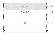
도 3은 도 1의 A 부분에서의 월 라이너(112)와 세라믹 박막(130)의 일 실시 예를 보여 준다.FIG. 3 shows an embodiment of the
도 1 및 도 3을 참조하면, 세라믹 박막(130)은 월 라이너(112) 상에 배치될 수 있다. 실질적으로, 월 라이너(112)의 상부 면은 챔버(100)의 내벽에 대응될 수 있다. 세라믹 박막(130)은 기판(10)으로부터 노출되는 정전 척(114) 상에 배치될 수 있다. 일 예에 따르면, 월 라이너(112)는 알루미늄(Al)을 포함할 수 있다. 예컨대, 알루미늄(Al)은 양극산화방법으로 형성될 수 있다. 세라믹 박막(130)은 이트륨 산소 불화막(YxOyFz, x=1, y=1, 2, z=1, 2: YOF, YO2F, 또는 YOF2)을 포함할 수 있다.Referring to FIGS. 1 and 3, the ceramic
YOF는 화학식1과 같이 결합될 수 있다.YOF can be combined as shown in Formula (1).

여기서, Y+는 이트륨 이온이다. 이트륨 이온(Y+)은 산소(O)와 불소(F)에 결합될 수 있다. 이트륨(Y)은 YOF 내에서 이온 상태로 존재하기 때문에 산소(O)와 불소(F)에 비해 높은 반응성을 가질 수 있다.Here, Y+ is yttrium ion. Yttrium ions (Y+ ) may be bonded to oxygen (O) and fluorine (F). Since yttrium (Y) exists in ionic state in YOF, it can have higher reactivity than oxygen (O) and fluorine (F).
YO2F는 화학식 2와 같이 결합될 수 있다. ,YO2 F may be combined as shown in formula (2). ,

이트륨(Y)은 2개의 산소(O)와 1개의 불소(F)에 공통으로 결합될 수 있다. 이트륨(Y)과 산소(O)의 결합(Y-O)은 이트륨(Y)과 불소(F)의 결합(Y-F)보다 많을 수 있다. YO2F는 불소(F)에 대해 YOF보다 낮은 반응성을 가질 수 있다.Yttrium (Y) may be commonly bonded to two oxygen (O) and one fluorine (F). The bond (YO) of yttrium (Y) and oxygen (O) may be larger than the bond (YF) of yttrium (Y) and fluorine (F). YO2 F may have lower reactivity than YOF for fluorine (F).
YOF2는 화학식 3과 같이 결합될 수 있다.YOF2 may be combined as shown in

이트륨(Y)는 1개의 산소(O)와 2개의 불소(F)에 결합될 수 있다. 이트륨(Y)과 불소(F)의 결합(Y-F)은 이트륨(Y)과 산소(O)의 결합(Y-O)보다 많을 수 있다. 이트륨(Y)과 산소(O)의 결합(Y-O) 중의 산소(O)는 YOF2의 부식을 감소시킬 수 있다. YOF2는 불소(F)에 대해 YO2F보다 낮은 반응성을 가질 수 있다.Yttrium (Y) may be bonded to one oxygen (O) and two fluorines (F). The bond (YF) of yttrium (Y) and fluorine (F) may be larger than the bond (YO) of yttrium (Y) and oxygen (O). Oxygen (O) in the bond (YO) of yttrium (Y) and oxygen (O) can reduce the corrosion of YOF2 . YOF2 may have a reactivity lower than YO2 F for fluorine (F).
이와 같은 이트륨 산소 불화막(YxOyFz)은 불소(F) 성분의 반응 가스에 대해 내화학성을 가질 수 있다. 반응 가스의 불소(F)와, 이트륨 산소 불화막(YxOyFz)의 관계는 후속에서 설명될 것이다.Such a yttrium oxyfluoride film (Yx Oy Fz ) may have chemical resistance to a reactive gas of a fluorine (F) component. The relationship between the fluorine (F) of the reaction gas and the yttrium oxyfluoride film (Yx Oy Fz ) will be described later.
도 4는 일반적인 세라믹 박막(130a)을 보여준다.Fig. 4 shows a general ceramic
도 4를 참조하면, 일반적인 세라믹 박막(130a)은 이트륨 산화막(Y2O3)을 포함할 수 있다. 이트륨 산화막(Y2O3)은 반응 가스에 의해 쉽게 손상될 수 있다. 반응 가스는 불소(F)를 포함할 수 있다. 불소(F)는 세라믹 박막(130a) 내의 이트륨(Y)과 결합될 수 있다. 세라믹 박막(130a)은 불소(F)와 이트륨(Y)의 결합(Y-F)에 따른 진행성 크랙(130b)을 가질 수 있다. 나아가, 진행성 크랙(130b)은 파티클 불량을 발생시킬 수 있다.Referring to FIG. 4, the general ceramic
도 5는 도 4의 일반적인 세라믹 박막(130a)의 XPS (X-ray photoelectron spectroscopy)의 깊이 프로파일(depth profile)이다.FIG. 5 is a depth profile of X-ray photoelectron spectroscopy (XPS) of the general ceramic
도 4 및 도 5를 참조하면, 일반적인 세라믹 박막(130a)이 반응 가스에 30시간이상 노출될 경우, 불소(F)는 세라믹 박막(130a)의 깊이 방향으로 20nm 깊이까지 우세한 양으로 침투된 후 점진적으로 감소할 수 있다. 불소(F)는 반응 가스에 의해 세라믹 박막(130a) 내에 침투될 수 있다. 침투된 불소(F)는 이트륨 산화막(Y2O3) 내에서 진행성 크랙(130b)의 발생원이 될 수 있다. 이트륨(Y)과 산소(O)는 깊이 방향으로 점진적으로 증가하고, 약 20nm이상의 깊이에서 유사한 성분비를 가질 수 있다.4 and 5, when the general ceramic
도 6은 도 3의 세라믹 박막(130)의 XPS (X-ray photoelectron spectroscopy)의 깊이 프로파일이다.FIG. 6 is a depth profile of an X-ray photoelectron spectroscopy (XPS) of the ceramic
도 3 및 도 6을 참조하면, 본 발명의 세라믹 박막(130)은 반응 가스에 10시간이상 노출되더라도 이트륨(Y), 산소(O), 및 불소(F)의 안정화된 상태를 가질 수 있다. 불소(F)는 약 200nm의 깊이까지 줄어들 수 있다. 불소(F)는 약 200nm 이상의 깊이에서 실질적으로 안정화된 성분비를 가질 수 있다. 세라믹 박막(130) 내의 불소(F)와 이트륨(Y)은 안정적인 결합 에너지를 가질 수 있다. 불소(F)와 이트륨(Y)은 반응 가스 노출 전 초기 상태와 유사한 수준을 유지할 수 있다. 세라믹 박막(130)은 반응 가스의 불소(F)의 침투를 방지할 수 있다. 불소(F)가 침투될 경우, 세라믹 박막(130)은 매우 작은 표면 화학적 변화를 갖기 때문에 진행성 크랙(130b)을 억제할 수 있다. 따라서, 세라믹 박막(130)은 반응 가스로에 의해 손상되지 않고, 파티클 발생을 최소화할 수 있다.Referring to FIGS. 3 and 6, the ceramic
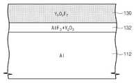
도 7은 도 1의 A 부분에서의 월 라이너(112)와 세라믹 박막(130)의 다른 실시 예를 보여준다.FIG. 7 shows another embodiment of the
도 7을 참조하면, 월 라이너(112)와 세라믹 박막(130) 사이에 완충 층(132)이 배치될 수 있다. 월 라이너(112)와 세라믹 층(130)은 도 3과 동일할 수 있다. 예를 들어, 완충 층(132)은 알루미늄 이트륨 산소 불화막(AlvYxOyFz, v=1, 2, x=1, y=1, 2, z=1, 2)을 포함할 수 있다. 완충 층(132) 내의 알루미늄(Al)은 알루미늄은 월 라이너(112)로 향할수록 증가하고, 불소(F)는 월 라이너(112)로 향할수록 감소할 수 있다. 일 에에 따르면, 완충 층(132)은 월 라이너(112)와 세라믹 박막(130)의 열팽창 계수 차이를 감소시킬 수 있다. 완충 층(132)의 열팽창 계수는 월 라이너(112)의 열팽창 계수보다 크고, 세라믹 박막(130)의 열팽창 계수보다 작을 수 있다. 알루미늄의 열팽창 계수는 22x10-6/K이고, 이트륨 산소 불화막의 열팽창 계수는 28x10-6/K일 수 있다. 알루미늄 이트륨 산소 불화막(AlvYxOyFz)의 열팽창 계수는 22x10-6/K보다 크고, 28x10-6/K보다 작을 수 있다.Referring to FIG. 7, a
도 8은 도 1의 A 부분에서의 월 라이너(112)와 세라믹 박막(130)의 또 다른 실시 예를 보여준다.Fig. 8 shows another embodiment of the
도 8을 참조하면, 완충 층(132)은 알루미늄 불화막(AlF3)과 이트륨 산화막(Y2O3)의 혼합 물(AlF3+Y2O3)을 포함할 수 있다. 혼합 물(AlF3+Y2O3)의 열팽창 계수는 알루미늄(Al)의 열팽창 계수보다 클 수 있다. 또한, 혼합 물(AlF3+Y2O3)의 열팽창 계수는 이트륨 산소 불화막(YxOyFz)의 열팽창 계수보다 작을 수 있다.Referring to FIG. 8, the
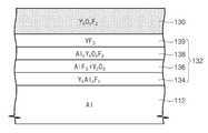
도 9는 도 1의 A 부분에서의 월 라이너(112)와 세라믹 박막(130)의 또 다른 실시 예를 보여준다.FIG. 9 shows another embodiment of the
도 9를 참조하면, 완충 층(132)은 제 1 완충 층(134), 제 2 완충 층(136), 및 제 4 완충 층(139)을 포함할 수 있다. 완충 층(132)은 월 라이너(112)와 세라믹 박막(130)의 열 팽창 계수의 차이를 순차적으로 줄일 수 있다. 제 1 완충 층(134)은 월 라이너(112) 상에 배치될 수 있다. 제 1 완충 층(134)의 열팽창 계수는 월 라이너(112)의 열팽창 계수보다는 클 수 있다. 제 1 완충 층(134)은 알루미늄 이트륨 불화막(AlvYxFz, v=1, 2, x=1, z=1, 2)을 포함할 수 있다. 제 2 완충 층(136)은 제 1 완충 층(134) 상에 배치될 수 있다. 제 2 완충 층(136)의 열팽창 계수는 제 1 완충 층(134)의 열팽창 계수보다 클 수 있다. 제 2 완충 층(136)은 알루미늄 불화막(AlF3)과 이트륨 산화막(Y2O3)의 혼합물(AlF3+Y2O3)을 포함할 수 있다. 제 3 완충 층(138)은 제 2 완충 층(136) 상에 배치될 수 있다. 제 3 완충 층(138)의 열팽창 계수는 제 2 완충 층(136)의 열팽창 계수보다 크고, 세라믹 박막(130)의 열팽창 계수보다 작을 수 있다. 제 3 완충 층(138)은 알루미늄 이트륨 산소 불화막(AlvYxOyFz, v=1, 2, x=1, y=1, 2, z=1, 2)을 포함할 수 있다. 알루미늄(Al)은 완충 층(132)의 깊이 방향으로 증가할 수 있다. 예를 들어, 알루미늄(Al)은 제 3 완충 층(138)보다 제 2 완충 층(136)에 많을 수 있다. 알루미늄(Al)은 제 2 완충 층(136)보다 제 2 완충 층(134)에 많을 수 있다. 반면, 불소(F)는 완충 층(132)의 깊이 방향으로 줄어들 수 있다. 불소(F)는 제 3 완 충 층(138)보다 제 2 완충 층(136)에 적을 수 있다. 불소(F)는 제 2 완 충 층(136)보다 제 1 완충 층(134)에 적을 수 있다. 제 4 완충 층(139)은 제 3 완충 층(138) 상에 배치될 수 있다. 제 4 완충 층(139)의 열팽창 계수는 제 3 완충 층(138)보다 크고, 세라믹 박막(130)의 열팽창 계수보다 작을 수 있다. 제 4 완충 층(139)은 이트륨 불화막(YF3)을 포함할 수 있다.Referring to FIG. 9, the
상술한 바와 같이, 세라믹 박막(130)은 도 4의 진행성 크랙(130b)을 억제할 수 있다. 이와 달리, 세라믹 박막(130)은 식각 속도 변화율을 최소화할 수 있다. 일반적인 세라믹 박막(130a)의 식각 속도 변화율은 식각 공정 초기에 약 5.8%로 높을 수 있다. 때문에, 일반적인 세라믹 박막(130a)은 약 5시간 정도의 시즈닝 공정을 요구할 수 있다. 반면, 본 발명의 세라믹 박막(130)의 식각 속도 변화율은 식각 공정 초기에 약 2.5%로 낮을 수 있다. 세라믹 박막(130)은 시즈닝 공정을 제거시킬 수 있다. 따라서, 본 발명의 시즈닝 공정 없이 식각 공정을 수행할 수 있기 때문에 공정 백업 시간을 단축할 수 있다. 공정 백업 시간은 예방 정비 후 식각 공정까지 소요되는 시간으로 정의될 수 있다.As described above, the ceramic
이와 같이 구성된 본 발명의 기판 제조 장치(500)의 세라믹 박막(130)의 코팅 방법을 설명하면 다음과 같다.A method of coating the ceramic
도 10은 본 발명의 세라믹 박막(130)의 코팅 방법의 일 예를 보여준다.10 shows an example of a coating method of the ceramic
도 10을 참조하면, 세라믹 박막(130)의 코팅 방법은 챔버(100)를 제공하는 단계(S10)와 세라믹 박막(130)을 형성하는 단계(S20)를 포함할 수 있다. 챔버(100)를 제공하는 단계(S10)는 챔버(100)의 예방 정비 단계를 포함할 수 있다. 예방 정비 단계는 습식 세정 단계일 수 있다. 세라믹 박막(130)을 형성하는 단계(S20)는 용사(thermal spraying) 방법, 에어로졸 방법, 전자빔 증착 방법, 또는 화학기상증착 방법 중 어느 하나를 포함할 수 있다.Referring to FIG. 10, a method of coating the ceramic
도 11은 도 10의 세라믹 박막(130)의 형성 단계(S20)를 보여주는 도면이다.11 is a view showing a forming step (S20) of the ceramic
도 11을 참조하면, 세라믹 박막(130)은 스프레이 건(140)에 의해 용사 방법으로 형성될 수 있다. 이트륨 산소 불화막 입자들(150)은 스토리지 부(142)를 통해 스프레이 건(142)에 제공될 수 있다. 스프레이 건(140)은 이트륨 산소 불화막 입자들(150)을 월 라이너(112)에 분사할 수 있다. 예를 들어, 이트륨 산소 불화막 입자들(150)은 10μm이하의 직경을 가질 수 있다. 스프레이 건(140)은 이트륨 산소 불화막 입자들(150)을 약 200°C이상으로 가열할 수 있다. 세라믹 박막(130)은 약 1%이하의 기공율을 갖도록 형성될 수 있다.Referring to FIG. 11, the ceramic
일 예에 따르면, 이트륨 산소 불화막 입자들(150)은 월 라이너(112) 및 세라믹 박막(130)에 약 45° 내지 약 90°의 분사각(θ)으로 입사될 수 있다. 이트륨 산소 불화막 입자들(150)이 0° 내지 45°의 분사각(θ)으로 입사될 경우, 세라믹 박막(130)의 코팅 불량이 발생될 수 있다. 예를 들어, 세라믹 박막(130)은 검은색의 표면 변색에 따른 코팅 불량을 가질 수 있다. 표면 변색은 세라믹 박막(130)의 표면 거칠기의 감소에 의해 방지될 수 있다. 감소된 표면 거칠기를 갖는 세라믹 박막(130)은 식각 공정 부산물들의 흡착 현상을 감소시킬 수 있다.According to one example, the yttrium
도 12는 본 발명의 세라믹 박막(130)의 코팅 방법의 다른 예를 보여준다.12 shows another example of a coating method of the ceramic
도 12를 참조하면, 세라믹 박막(130)의 코팅 방법은 챔버(100)를 제공하는 단계(S10), 완충 층(132)을 형성하는 단계(S12), 및 세라믹 박막(130)을 형성하는 단계(S20)를 포함할 수 있다. 챔버(100)를 제공하는 단계(S10), 및 세라믹 박막(130)을 형성하는 단계(S20)는 도 10과 동일할 수 있다.12, the method of coating the ceramic
완충 층(132)을 형성하는 단계(S12)는 제 1 내지 제 3 완충 층들(134, 136, 138, 139)을 형성하는 단계들(S14, S16, S18, S19)을 포함할 수 있다. 제 1 완충 층(134)을 형성하는 단계(S14)는 월 라이너(112) 상에 알루미늄 이트륨 불화막(AlvYxFz)을 형성하는 단계를 포함할 수 있다. 제 2 완충 층(136)을 형성하는 단계(S16)는 제 1 완충 층(134) 상에 알루미늄 불화막(AlF3)과 이트륨 산화막(Y2O3)의 혼합물(AlF3+Y2O3)을 형성하는 단계를 포함할 수 있다. 제 3 완충 층(138)을 형성하는 단계(S18)는 제 2 완충 층(136) 상에 알루미늄 이트륨 산소 불화막(AlvYxOyFz)을 형성하는 단계를 포함할 수 있다. 제 4 완충 층(139)을 형성하는 단계(S19)는 제 3 완충 층(138) 상에 이트륨 불화막(YF3)을 형성하는 단계를 포함할 수 있다.The step S12 of forming the
이상, 첨부된 도면들을 참조하여 본 발명의 실시 예들을 예를 설명하였지만, 본 발명이 속하는 기술분야에서 통상의 지식을 가진 자는 본 발명이 그 기술적 사상이나 필수적인 특징을 변경하지 않고서 다른 구체적인 형태로 실시될 수 있다는 것을 이해할 수 있을 것이다. 그러므로 이상에서 기술한 실시 예들 및 응용 예에는 모든 면에서 예시적인 것이며 한정적이 아닌 것으로 이해해야만 한다.While the present invention has been particularly shown and described with reference to exemplary embodiments thereof, it is to be understood that the invention is not limited to the exemplary embodiments or constructions. It can be understood that It is therefore to be understood that the above-described embodiments and applications are illustrative in all aspects and not restrictive.
Claims (10)
Translated fromKorean상기 챔버의 내벽 상의 세라믹 박막을 포함하되,
상기 세라믹 박막은 이트륨 산소 불화막(YxOyFz, x=1, y=1, 2, z=1, 2)을 포함하는 기판 제조 장치.chamber; And
And a ceramic thin film on the inner wall of the chamber,
Wherein the ceramic thin film comprises a yttrium oxyfluoride film (Yx Oy Fz , x = 1, y = 1, 2, z = 1, 2).
상기 내벽은 알루미늄을 포함하되,
상기 장치는 상기 내벽과 상기 세라믹 박막 사이에 배치되어 상기 이트륨 산소 불화막과 상기 알루미늄의 열팽창 계수의 차이를 감소시키는 완충 층을 더 포함하는 기판 제조 장치.The method according to claim 1,
Wherein the inner wall comprises aluminum,
Wherein the apparatus further comprises a buffer layer disposed between the inner wall and the ceramic thin film to reduce a difference in thermal expansion coefficient between the yttrium oxyfluoride film and the aluminum.
상기 완충 층은 알루미늄 이트륨 산소 산화막(AlvYxOyFz, v=1, 2, x=1, y=1, 2, z=1, 2)을 포함하는 기판 제조 장치.3. The method of claim 2,
Wherein the buffer layer comprises an aluminum yttrium oxide film (Alv Yx Oy Fz , v = 1, 2, x = 1, y = 1, 2, z = 1, 2).
상기 완충 층은 알루미늄 불화막과 이트륨 산화막의 혼합물을 포함하는 기판 제조 장치.3. The method of claim 2,
Wherein the buffer layer comprises a mixture of an aluminum fluoride film and a yttrium oxide film.
상기 완충 층은:
상기 내벽 상의 제 1 완충 층;
상기 제 1 완충 층 상의 제 2 완충 층;
상기 제 2 완충 층 상의 제 3 완층 층; 및
상기 제 3 완충 층 상의 제 4 완층 층을 포함하되,
상기 제 1 완충 층은 알루미늄 이트륨 불화막을 포함하는 기판 제조 장치.3. The method of claim 2,
The buffer layer comprises:
A first buffer layer on the inner wall;
A second buffer layer on the first buffer layer;
A third complete layer on the second buffer layer; And
And a fourth complete layer on the third buffer layer,
Wherein the first buffer layer comprises an aluminum yttrium fluoride film.
상기 제 2 완충 층은 알루미늄 불화막과 이트륨 산화막의 혼합물을 포함하는 기판 제조 장치.6. The method of claim 5,
Wherein the second buffer layer comprises a mixture of an aluminum fluoride film and a yttrium oxide film.
상기 제 3 완충 층은 알루미늄 이트륨 산소 불화막을 포함하는 기판 제조 장치.6. The method of claim 5,
Wherein the third buffer layer comprises an aluminum yttrium oxygen fluoride film.
상기 제 4 완충 층은 이트륨 불화막을 포함하는 기판 제조 장치.6. The method of claim 5,
Wherein the fourth buffer layer comprises a yttrium fluoride film.
상기 챔버의 내벽에 세라믹 박막을 형성하는 단계를 포함하되,
상기 세라믹 박막을 형성하는 단계는 이트륨 산소 불화막(YxOyFz, x=1, y=1, 2, z=1, 2)을 형성하는 단계를 포함하는 기판 제조 장치의 세라믹 박막 코팅 방법.Providing a chamber; And
And forming a ceramic thin film on an inner wall of the chamber,
Wherein the step of forming the ceramic thin film comprises forming a yttrium oxygen fluoride film (Yx Oy Fz , x = 1, y = 1, 2, z = 1, 2) Way.
상기 챔버 상에 알루미늄 이트륨 불화막을 포함하는 제 1 완충 층을 형성하는 단계;
상기 제 1 완충 층 상에 알루미늄 불화막과 이트륨 산화막의 혼합물을 포함하는 제 2 완충 층을 형성하는 단계;
상기 제 2 완충 층 상에 알루미늄 이트륨 산소 불화막을 포함하는 제 3 완충 층을 형성하는 단계; 및
상기 제 3 완충 층 상에 이트륨 불화막을 포함하는 제 4 완충 층을 형성하는 단계를 포함하는 기판 제조 장치의 세라믹 박막 코팅 방법.10. The method of claim 9,
Forming a first buffer layer comprising an aluminum yttrium fluoride film on the chamber;
Forming a second buffer layer on the first buffer layer, the second buffer layer including a mixture of an aluminum fluoride film and a yttrium oxide film;
Forming a third buffer layer on the second buffer layer, the third buffer layer including an aluminum yttrium oxyfluoride film; And
And forming a fourth buffer layer including a yttrium fluoride film on the third buffer layer.
Priority Applications (2)
| Application Number | Priority Date | Filing Date | Title |
|---|---|---|---|
| KR1020150055418AKR20160124992A (en) | 2015-04-20 | 2015-04-20 | apparatus for manufacturing a substrate and ceramic film coating method of the same |
| US15/092,965US20160307740A1 (en) | 2015-04-20 | 2016-04-07 | Substrate Processing System and Ceramic Coating Method Therefor |
Applications Claiming Priority (1)
| Application Number | Priority Date | Filing Date | Title |
|---|---|---|---|
| KR1020150055418AKR20160124992A (en) | 2015-04-20 | 2015-04-20 | apparatus for manufacturing a substrate and ceramic film coating method of the same |
Publications (1)
| Publication Number | Publication Date |
|---|---|
| KR20160124992Atrue KR20160124992A (en) | 2016-10-31 |
Family
ID=57129235
Family Applications (1)
| Application Number | Title | Priority Date | Filing Date |
|---|---|---|---|
| KR1020150055418AWithdrawnKR20160124992A (en) | 2015-04-20 | 2015-04-20 | apparatus for manufacturing a substrate and ceramic film coating method of the same |
Country Status (2)
| Country | Link |
|---|---|
| US (1) | US20160307740A1 (en) |
| KR (1) | KR20160124992A (en) |
Cited By (2)
| Publication number | Priority date | Publication date | Assignee | Title |
|---|---|---|---|---|
| KR20180000309A (en)* | 2016-06-22 | 2018-01-02 | 니혼도꾸슈도교 가부시키가이샤 | Yttrium oxyfluoride sprayed coating and method for producing the same, and sprayed member |
| CN116092909A (en)* | 2017-12-12 | 2023-05-09 | 中微半导体设备(上海)股份有限公司 | Plasma etching reactor |
Families Citing this family (259)
| Publication number | Priority date | Publication date | Assignee | Title |
|---|---|---|---|---|
| US20130023129A1 (en) | 2011-07-20 | 2013-01-24 | Asm America, Inc. | Pressure transmitter for a semiconductor processing environment |
| US10714315B2 (en) | 2012-10-12 | 2020-07-14 | Asm Ip Holdings B.V. | Semiconductor reaction chamber showerhead |
| US20160376700A1 (en) | 2013-02-01 | 2016-12-29 | Asm Ip Holding B.V. | System for treatment of deposition reactor |
| US10941490B2 (en) | 2014-10-07 | 2021-03-09 | Asm Ip Holding B.V. | Multiple temperature range susceptor, assembly, reactor and system including the susceptor, and methods of using the same |
| US10276355B2 (en) | 2015-03-12 | 2019-04-30 | Asm Ip Holding B.V. | Multi-zone reactor, system including the reactor, and method of using the same |
| US10458018B2 (en) | 2015-06-26 | 2019-10-29 | Asm Ip Holding B.V. | Structures including metal carbide material, devices including the structures, and methods of forming same |
| US10211308B2 (en) | 2015-10-21 | 2019-02-19 | Asm Ip Holding B.V. | NbMC layers |
| US11139308B2 (en) | 2015-12-29 | 2021-10-05 | Asm Ip Holding B.V. | Atomic layer deposition of III-V compounds to form V-NAND devices |
| US10529554B2 (en) | 2016-02-19 | 2020-01-07 | Asm Ip Holding B.V. | Method for forming silicon nitride film selectively on sidewalls or flat surfaces of trenches |
| US10343920B2 (en) | 2016-03-18 | 2019-07-09 | Asm Ip Holding B.V. | Aligned carbon nanotubes |
| US11572617B2 (en)* | 2016-05-03 | 2023-02-07 | Applied Materials, Inc. | Protective metal oxy-fluoride coatings |
| US11453943B2 (en) | 2016-05-25 | 2022-09-27 | Asm Ip Holding B.V. | Method for forming carbon-containing silicon/metal oxide or nitride film by ALD using silicon precursor and hydrocarbon precursor |
| US10538845B2 (en)* | 2016-06-22 | 2020-01-21 | Ngk Spark Plug Co., Ltd. | Yttrium oxyfluoride sprayed coating and method for producing the same, and sprayed member |
| US10612137B2 (en) | 2016-07-08 | 2020-04-07 | Asm Ip Holdings B.V. | Organic reactants for atomic layer deposition |
| US9859151B1 (en) | 2016-07-08 | 2018-01-02 | Asm Ip Holding B.V. | Selective film deposition method to form air gaps |
| US9812320B1 (en) | 2016-07-28 | 2017-11-07 | Asm Ip Holding B.V. | Method and apparatus for filling a gap |
| US9887082B1 (en) | 2016-07-28 | 2018-02-06 | Asm Ip Holding B.V. | Method and apparatus for filling a gap |
| TWI721216B (en)* | 2016-10-13 | 2021-03-11 | 美商應用材料股份有限公司 | A chamber component for use in a plasma processing apparatus, an apparatus comprising the same, and a method for fabricating the same |
| US11532757B2 (en) | 2016-10-27 | 2022-12-20 | Asm Ip Holding B.V. | Deposition of charge trapping layers |
| US10714350B2 (en) | 2016-11-01 | 2020-07-14 | ASM IP Holdings, B.V. | Methods for forming a transition metal niobium nitride film on a substrate by atomic layer deposition and related semiconductor device structures |
| KR102546317B1 (en) | 2016-11-15 | 2023-06-21 | 에이에스엠 아이피 홀딩 비.브이. | Gas supply unit and substrate processing apparatus including the same |
| KR102762543B1 (en) | 2016-12-14 | 2025-02-05 | 에이에스엠 아이피 홀딩 비.브이. | Substrate processing apparatus |
| US11447861B2 (en) | 2016-12-15 | 2022-09-20 | Asm Ip Holding B.V. | Sequential infiltration synthesis apparatus and a method of forming a patterned structure |
| US11581186B2 (en) | 2016-12-15 | 2023-02-14 | Asm Ip Holding B.V. | Sequential infiltration synthesis apparatus |
| US10269558B2 (en) | 2016-12-22 | 2019-04-23 | Asm Ip Holding B.V. | Method of forming a structure on a substrate |
| US11390950B2 (en) | 2017-01-10 | 2022-07-19 | Asm Ip Holding B.V. | Reactor system and method to reduce residue buildup during a film deposition process |
| US10468261B2 (en) | 2017-02-15 | 2019-11-05 | Asm Ip Holding B.V. | Methods for forming a metallic film on a substrate by cyclical deposition and related semiconductor device structures |
| US10770286B2 (en) | 2017-05-08 | 2020-09-08 | Asm Ip Holdings B.V. | Methods for selectively forming a silicon nitride film on a substrate and related semiconductor device structures |
| US20180327892A1 (en)* | 2017-05-10 | 2018-11-15 | Applied Materials, Inc. | Metal oxy-flouride films for chamber components |
| US12040200B2 (en) | 2017-06-20 | 2024-07-16 | Asm Ip Holding B.V. | Semiconductor processing apparatus and methods for calibrating a semiconductor processing apparatus |
| US11306395B2 (en) | 2017-06-28 | 2022-04-19 | Asm Ip Holding B.V. | Methods for depositing a transition metal nitride film on a substrate by atomic layer deposition and related deposition apparatus |
| KR20190009245A (en) | 2017-07-18 | 2019-01-28 | 에이에스엠 아이피 홀딩 비.브이. | Methods for forming a semiconductor device structure and related semiconductor device structures |
| US11374112B2 (en) | 2017-07-19 | 2022-06-28 | Asm Ip Holding B.V. | Method for depositing a group IV semiconductor and related semiconductor device structures |
| US10590535B2 (en) | 2017-07-26 | 2020-03-17 | Asm Ip Holdings B.V. | Chemical treatment, deposition and/or infiltration apparatus and method for using the same |
| TWI815813B (en) | 2017-08-04 | 2023-09-21 | 荷蘭商Asm智慧財產控股公司 | Showerhead assembly for distributing a gas within a reaction chamber |
| US10692741B2 (en) | 2017-08-08 | 2020-06-23 | Asm Ip Holdings B.V. | Radiation shield |
| US10770336B2 (en) | 2017-08-08 | 2020-09-08 | Asm Ip Holding B.V. | Substrate lift mechanism and reactor including same |
| US11769682B2 (en) | 2017-08-09 | 2023-09-26 | Asm Ip Holding B.V. | Storage apparatus for storing cassettes for substrates and processing apparatus equipped therewith |
| US11830730B2 (en) | 2017-08-29 | 2023-11-28 | Asm Ip Holding B.V. | Layer forming method and apparatus |
| US11295980B2 (en) | 2017-08-30 | 2022-04-05 | Asm Ip Holding B.V. | Methods for depositing a molybdenum metal film over a dielectric surface of a substrate by a cyclical deposition process and related semiconductor device structures |
| US10658205B2 (en) | 2017-09-28 | 2020-05-19 | Asm Ip Holdings B.V. | Chemical dispensing apparatus and methods for dispensing a chemical to a reaction chamber |
| US10403504B2 (en) | 2017-10-05 | 2019-09-03 | Asm Ip Holding B.V. | Method for selectively depositing a metallic film on a substrate |
| US10923344B2 (en) | 2017-10-30 | 2021-02-16 | Asm Ip Holding B.V. | Methods for forming a semiconductor structure and related semiconductor structures |
| WO2019103613A1 (en) | 2017-11-27 | 2019-05-31 | Asm Ip Holding B.V. | A storage device for storing wafer cassettes for use with a batch furnace |
| CN111344522B (en) | 2017-11-27 | 2022-04-12 | 阿斯莫Ip控股公司 | Including clean mini-environment device |
| US10872771B2 (en) | 2018-01-16 | 2020-12-22 | Asm Ip Holding B. V. | Method for depositing a material film on a substrate within a reaction chamber by a cyclical deposition process and related device structures |
| KR102695659B1 (en) | 2018-01-19 | 2024-08-14 | 에이에스엠 아이피 홀딩 비.브이. | Method for depositing a gap filling layer by plasma assisted deposition |
| TWI799494B (en) | 2018-01-19 | 2023-04-21 | 荷蘭商Asm 智慧財產控股公司 | Deposition method |
| US11081345B2 (en) | 2018-02-06 | 2021-08-03 | Asm Ip Holding B.V. | Method of post-deposition treatment for silicon oxide film |
| WO2019158960A1 (en) | 2018-02-14 | 2019-08-22 | Asm Ip Holding B.V. | A method for depositing a ruthenium-containing film on a substrate by a cyclical deposition process |
| US10896820B2 (en) | 2018-02-14 | 2021-01-19 | Asm Ip Holding B.V. | Method for depositing a ruthenium-containing film on a substrate by a cyclical deposition process |
| US10731249B2 (en) | 2018-02-15 | 2020-08-04 | Asm Ip Holding B.V. | Method of forming a transition metal containing film on a substrate by a cyclical deposition process, a method for supplying a transition metal halide compound to a reaction chamber, and related vapor deposition apparatus |
| KR102636427B1 (en) | 2018-02-20 | 2024-02-13 | 에이에스엠 아이피 홀딩 비.브이. | Substrate processing method and apparatus |
| US10975470B2 (en) | 2018-02-23 | 2021-04-13 | Asm Ip Holding B.V. | Apparatus for detecting or monitoring for a chemical precursor in a high temperature environment |
| US11473195B2 (en) | 2018-03-01 | 2022-10-18 | Asm Ip Holding B.V. | Semiconductor processing apparatus and a method for processing a substrate |
| US11629406B2 (en) | 2018-03-09 | 2023-04-18 | Asm Ip Holding B.V. | Semiconductor processing apparatus comprising one or more pyrometers for measuring a temperature of a substrate during transfer of the substrate |
| KR102646467B1 (en) | 2018-03-27 | 2024-03-11 | 에이에스엠 아이피 홀딩 비.브이. | Method of forming an electrode on a substrate and a semiconductor device structure including an electrode |
| US11230766B2 (en) | 2018-03-29 | 2022-01-25 | Asm Ip Holding B.V. | Substrate processing apparatus and method |
| KR102600229B1 (en) | 2018-04-09 | 2023-11-10 | 에이에스엠 아이피 홀딩 비.브이. | Substrate supporting device, substrate processing apparatus including the same and substrate processing method |
| TWI811348B (en) | 2018-05-08 | 2023-08-11 | 荷蘭商Asm 智慧財產控股公司 | Methods for depositing an oxide film on a substrate by a cyclical deposition process and related device structures |
| US12025484B2 (en) | 2018-05-08 | 2024-07-02 | Asm Ip Holding B.V. | Thin film forming method |
| US12272527B2 (en) | 2018-05-09 | 2025-04-08 | Asm Ip Holding B.V. | Apparatus for use with hydrogen radicals and method of using same |
| KR102596988B1 (en) | 2018-05-28 | 2023-10-31 | 에이에스엠 아이피 홀딩 비.브이. | Method of processing a substrate and a device manufactured by the same |
| TWI840362B (en) | 2018-06-04 | 2024-05-01 | 荷蘭商Asm Ip私人控股有限公司 | Wafer handling chamber with moisture reduction |
| US11718913B2 (en) | 2018-06-04 | 2023-08-08 | Asm Ip Holding B.V. | Gas distribution system and reactor system including same |
| US11286562B2 (en) | 2018-06-08 | 2022-03-29 | Asm Ip Holding B.V. | Gas-phase chemical reactor and method of using same |
| KR102568797B1 (en) | 2018-06-21 | 2023-08-21 | 에이에스엠 아이피 홀딩 비.브이. | Substrate processing system |
| US10797133B2 (en) | 2018-06-21 | 2020-10-06 | Asm Ip Holding B.V. | Method for depositing a phosphorus doped silicon arsenide film and related semiconductor device structures |
| TWI873894B (en) | 2018-06-27 | 2025-02-21 | 荷蘭商Asm Ip私人控股有限公司 | Cyclic deposition methods for forming metal-containing material and films and structures including the metal-containing material |
| KR102854019B1 (en) | 2018-06-27 | 2025-09-02 | 에이에스엠 아이피 홀딩 비.브이. | Periodic deposition method for forming a metal-containing material and films and structures comprising the metal-containing material |
| US10612136B2 (en) | 2018-06-29 | 2020-04-07 | ASM IP Holding, B.V. | Temperature-controlled flange and reactor system including same |
| US10388513B1 (en) | 2018-07-03 | 2019-08-20 | Asm Ip Holding B.V. | Method for depositing silicon-free carbon-containing film as gap-fill layer by pulse plasma-assisted deposition |
| US10755922B2 (en) | 2018-07-03 | 2020-08-25 | Asm Ip Holding B.V. | Method for depositing silicon-free carbon-containing film as gap-fill layer by pulse plasma-assisted deposition |
| US20200024735A1 (en)* | 2018-07-18 | 2020-01-23 | Applied Materials, Inc. | Erosion resistant metal fluoride coatings deposited by atomic layer deposition |
| US11430674B2 (en) | 2018-08-22 | 2022-08-30 | Asm Ip Holding B.V. | Sensor array, apparatus for dispensing a vapor phase reactant to a reaction chamber and related methods |
| KR102707956B1 (en) | 2018-09-11 | 2024-09-19 | 에이에스엠 아이피 홀딩 비.브이. | Method for deposition of a thin film |
| US11024523B2 (en) | 2018-09-11 | 2021-06-01 | Asm Ip Holding B.V. | Substrate processing apparatus and method |
| CN110970344B (en) | 2018-10-01 | 2024-10-25 | Asmip控股有限公司 | Substrate holding apparatus, system comprising the same and method of using the same |
| US11232963B2 (en) | 2018-10-03 | 2022-01-25 | Asm Ip Holding B.V. | Substrate processing apparatus and method |
| KR102592699B1 (en) | 2018-10-08 | 2023-10-23 | 에이에스엠 아이피 홀딩 비.브이. | Substrate support unit and apparatuses for depositing thin film and processing the substrate including the same |
| KR102605121B1 (en) | 2018-10-19 | 2023-11-23 | 에이에스엠 아이피 홀딩 비.브이. | Substrate processing apparatus and substrate processing method |
| KR102546322B1 (en) | 2018-10-19 | 2023-06-21 | 에이에스엠 아이피 홀딩 비.브이. | Substrate processing apparatus and substrate processing method |
| US12378665B2 (en)* | 2018-10-26 | 2025-08-05 | Asm Ip Holding B.V. | High temperature coatings for a preclean and etch apparatus and related methods |
| US11087997B2 (en) | 2018-10-31 | 2021-08-10 | Asm Ip Holding B.V. | Substrate processing apparatus for processing substrates |
| KR102748291B1 (en) | 2018-11-02 | 2024-12-31 | 에이에스엠 아이피 홀딩 비.브이. | Substrate support unit and substrate processing apparatus including the same |
| US11572620B2 (en) | 2018-11-06 | 2023-02-07 | Asm Ip Holding B.V. | Methods for selectively depositing an amorphous silicon film on a substrate |
| US10818758B2 (en) | 2018-11-16 | 2020-10-27 | Asm Ip Holding B.V. | Methods for forming a metal silicate film on a substrate in a reaction chamber and related semiconductor device structures |
| US12040199B2 (en) | 2018-11-28 | 2024-07-16 | Asm Ip Holding B.V. | Substrate processing apparatus for processing substrates |
| US11217444B2 (en) | 2018-11-30 | 2022-01-04 | Asm Ip Holding B.V. | Method for forming an ultraviolet radiation responsive metal oxide-containing film |
| KR102636428B1 (en) | 2018-12-04 | 2024-02-13 | 에이에스엠 아이피 홀딩 비.브이. | A method for cleaning a substrate processing apparatus |
| US11158513B2 (en) | 2018-12-13 | 2021-10-26 | Asm Ip Holding B.V. | Methods for forming a rhenium-containing film on a substrate by a cyclical deposition process and related semiconductor device structures |
| TWI874340B (en) | 2018-12-14 | 2025-03-01 | 荷蘭商Asm Ip私人控股有限公司 | Method of forming device structure, structure formed by the method and system for performing the method |
| TWI866480B (en) | 2019-01-17 | 2024-12-11 | 荷蘭商Asm Ip 私人控股有限公司 | Methods of forming a transition metal containing film on a substrate by a cyclical deposition process |
| KR102727227B1 (en) | 2019-01-22 | 2024-11-07 | 에이에스엠 아이피 홀딩 비.브이. | Semiconductor processing device |
| TWI838458B (en) | 2019-02-20 | 2024-04-11 | 荷蘭商Asm Ip私人控股有限公司 | Apparatus and methods for plug fill deposition in 3-d nand applications |
| KR102626263B1 (en) | 2019-02-20 | 2024-01-16 | 에이에스엠 아이피 홀딩 비.브이. | Cyclical deposition method including treatment step and apparatus for same |
| TWI873122B (en) | 2019-02-20 | 2025-02-21 | 荷蘭商Asm Ip私人控股有限公司 | Method of filling a recess formed within a surface of a substrate, semiconductor structure formed according to the method, and semiconductor processing apparatus |
| TWI845607B (en) | 2019-02-20 | 2024-06-21 | 荷蘭商Asm Ip私人控股有限公司 | Cyclical deposition method and apparatus for filling a recess formed within a substrate surface |
| TWI842826B (en) | 2019-02-22 | 2024-05-21 | 荷蘭商Asm Ip私人控股有限公司 | Substrate processing apparatus and method for processing substrate |
| KR102858005B1 (en) | 2019-03-08 | 2025-09-09 | 에이에스엠 아이피 홀딩 비.브이. | Method for Selective Deposition of Silicon Nitride Layer and Structure Including Selectively-Deposited Silicon Nitride Layer |
| US11742198B2 (en) | 2019-03-08 | 2023-08-29 | Asm Ip Holding B.V. | Structure including SiOCN layer and method of forming same |
| JP2020167398A (en) | 2019-03-28 | 2020-10-08 | エーエスエム・アイピー・ホールディング・ベー・フェー | Door openers and substrate processing equipment provided with door openers |
| KR102809999B1 (en) | 2019-04-01 | 2025-05-19 | 에이에스엠 아이피 홀딩 비.브이. | Method of manufacturing semiconductor device |
| KR20200123380A (en) | 2019-04-19 | 2020-10-29 | 에이에스엠 아이피 홀딩 비.브이. | Layer forming method and apparatus |
| KR20200125453A (en) | 2019-04-24 | 2020-11-04 | 에이에스엠 아이피 홀딩 비.브이. | Gas-phase reactor system and method of using same |
| KR20200130121A (en) | 2019-05-07 | 2020-11-18 | 에이에스엠 아이피 홀딩 비.브이. | Chemical source vessel with dip tube |
| US11289326B2 (en) | 2019-05-07 | 2022-03-29 | Asm Ip Holding B.V. | Method for reforming amorphous carbon polymer film |
| KR20200130652A (en) | 2019-05-10 | 2020-11-19 | 에이에스엠 아이피 홀딩 비.브이. | Method of depositing material onto a surface and structure formed according to the method |
| JP7612342B2 (en) | 2019-05-16 | 2025-01-14 | エーエスエム・アイピー・ホールディング・ベー・フェー | Wafer boat handling apparatus, vertical batch furnace and method |
| JP7598201B2 (en) | 2019-05-16 | 2024-12-11 | エーエスエム・アイピー・ホールディング・ベー・フェー | Wafer boat handling apparatus, vertical batch furnace and method |
| USD947913S1 (en) | 2019-05-17 | 2022-04-05 | Asm Ip Holding B.V. | Susceptor shaft |
| USD975665S1 (en) | 2019-05-17 | 2023-01-17 | Asm Ip Holding B.V. | Susceptor shaft |
| KR20200141002A (en) | 2019-06-06 | 2020-12-17 | 에이에스엠 아이피 홀딩 비.브이. | Method of using a gas-phase reactor system including analyzing exhausted gas |
| KR20200141931A (en) | 2019-06-10 | 2020-12-21 | 에이에스엠 아이피 홀딩 비.브이. | Method for cleaning quartz epitaxial chambers |
| KR20200143254A (en) | 2019-06-11 | 2020-12-23 | 에이에스엠 아이피 홀딩 비.브이. | Method of forming an electronic structure using an reforming gas, system for performing the method, and structure formed using the method |
| USD944946S1 (en) | 2019-06-14 | 2022-03-01 | Asm Ip Holding B.V. | Shower plate |
| KR20210005515A (en) | 2019-07-03 | 2021-01-14 | 에이에스엠 아이피 홀딩 비.브이. | Temperature control assembly for substrate processing apparatus and method of using same |
| JP7499079B2 (en) | 2019-07-09 | 2024-06-13 | エーエスエム・アイピー・ホールディング・ベー・フェー | Plasma device using coaxial waveguide and substrate processing method |
| CN112216646A (en) | 2019-07-10 | 2021-01-12 | Asm Ip私人控股有限公司 | Substrate supporting assembly and substrate processing device comprising same |
| KR20210010307A (en) | 2019-07-16 | 2021-01-27 | 에이에스엠 아이피 홀딩 비.브이. | Substrate processing apparatus |
| KR102860110B1 (en) | 2019-07-17 | 2025-09-16 | 에이에스엠 아이피 홀딩 비.브이. | Methods of forming silicon germanium structures |
| KR20210010816A (en) | 2019-07-17 | 2021-01-28 | 에이에스엠 아이피 홀딩 비.브이. | Radical assist ignition plasma system and method |
| US11643724B2 (en) | 2019-07-18 | 2023-05-09 | Asm Ip Holding B.V. | Method of forming structures using a neutral beam |
| KR20210010817A (en) | 2019-07-19 | 2021-01-28 | 에이에스엠 아이피 홀딩 비.브이. | Method of Forming Topology-Controlled Amorphous Carbon Polymer Film |
| TWI839544B (en) | 2019-07-19 | 2024-04-21 | 荷蘭商Asm Ip私人控股有限公司 | Method of forming topology-controlled amorphous carbon polymer film |
| TWI851767B (en) | 2019-07-29 | 2024-08-11 | 荷蘭商Asm Ip私人控股有限公司 | Methods for selective deposition utilizing n-type dopants and/or alternative dopants to achieve high dopant incorporation |
| CN112309899A (en) | 2019-07-30 | 2021-02-02 | Asm Ip私人控股有限公司 | Substrate processing apparatus |
| CN112309900A (en) | 2019-07-30 | 2021-02-02 | Asm Ip私人控股有限公司 | Substrate processing apparatus |
| US12169361B2 (en) | 2019-07-30 | 2024-12-17 | Asm Ip Holding B.V. | Substrate processing apparatus and method |
| US11587814B2 (en) | 2019-07-31 | 2023-02-21 | Asm Ip Holding B.V. | Vertical batch furnace assembly |
| US11227782B2 (en) | 2019-07-31 | 2022-01-18 | Asm Ip Holding B.V. | Vertical batch furnace assembly |
| US11587815B2 (en) | 2019-07-31 | 2023-02-21 | Asm Ip Holding B.V. | Vertical batch furnace assembly |
| CN112323048B (en) | 2019-08-05 | 2024-02-09 | Asm Ip私人控股有限公司 | Liquid level sensor for chemical source container |
| CN112342526A (en) | 2019-08-09 | 2021-02-09 | Asm Ip私人控股有限公司 | Heater assembly including cooling device and method of using same |
| USD965044S1 (en) | 2019-08-19 | 2022-09-27 | Asm Ip Holding B.V. | Susceptor shaft |
| USD965524S1 (en) | 2019-08-19 | 2022-10-04 | Asm Ip Holding B.V. | Susceptor support |
| JP2021031769A (en) | 2019-08-21 | 2021-03-01 | エーエスエム アイピー ホールディング ビー.ブイ. | Production apparatus of mixed gas of film deposition raw material and film deposition apparatus |
| KR20210024423A (en) | 2019-08-22 | 2021-03-05 | 에이에스엠 아이피 홀딩 비.브이. | Method for forming a structure with a hole |
| USD979506S1 (en) | 2019-08-22 | 2023-02-28 | Asm Ip Holding B.V. | Insulator |
| USD940837S1 (en) | 2019-08-22 | 2022-01-11 | Asm Ip Holding B.V. | Electrode |
| USD949319S1 (en) | 2019-08-22 | 2022-04-19 | Asm Ip Holding B.V. | Exhaust duct |
| US11286558B2 (en) | 2019-08-23 | 2022-03-29 | Asm Ip Holding B.V. | Methods for depositing a molybdenum nitride film on a surface of a substrate by a cyclical deposition process and related semiconductor device structures including a molybdenum nitride film |
| KR20210024420A (en) | 2019-08-23 | 2021-03-05 | 에이에스엠 아이피 홀딩 비.브이. | Method for depositing silicon oxide film having improved quality by peald using bis(diethylamino)silane |
| KR102806450B1 (en) | 2019-09-04 | 2025-05-12 | 에이에스엠 아이피 홀딩 비.브이. | Methods for selective deposition using a sacrificial capping layer |
| KR102733104B1 (en) | 2019-09-05 | 2024-11-22 | 에이에스엠 아이피 홀딩 비.브이. | Substrate processing apparatus |
| CN110534427B (en)* | 2019-09-06 | 2021-11-12 | 上海华虹宏力半导体制造有限公司 | Etching method |
| US11976357B2 (en) | 2019-09-09 | 2024-05-07 | Applied Materials, Inc. | Methods for forming a protective coating on processing chamber surfaces or components |
| US11562901B2 (en) | 2019-09-25 | 2023-01-24 | Asm Ip Holding B.V. | Substrate processing method |
| CN112593212B (en) | 2019-10-02 | 2023-12-22 | Asm Ip私人控股有限公司 | Method for forming topologically selective silicon oxide film by cyclic plasma enhanced deposition process |
| TW202128273A (en) | 2019-10-08 | 2021-08-01 | 荷蘭商Asm Ip私人控股有限公司 | Gas injection system, reactor system, and method of depositing material on surface of substratewithin reaction chamber |
| TWI846953B (en) | 2019-10-08 | 2024-07-01 | 荷蘭商Asm Ip私人控股有限公司 | Substrate processing device |
| KR20210042810A (en) | 2019-10-08 | 2021-04-20 | 에이에스엠 아이피 홀딩 비.브이. | Reactor system including a gas distribution assembly for use with activated species and method of using same |
| TWI846966B (en) | 2019-10-10 | 2024-07-01 | 荷蘭商Asm Ip私人控股有限公司 | Method of forming a photoresist underlayer and structure including same |
| US11424140B2 (en) | 2019-10-10 | 2022-08-23 | Samsung Electronics Co., Ltd. | Member, method of manufacturing the same, apparatus for manufacturing the same, and semiconductor manufacturing apparatus |
| US12009241B2 (en) | 2019-10-14 | 2024-06-11 | Asm Ip Holding B.V. | Vertical batch furnace assembly with detector to detect cassette |
| TWI834919B (en) | 2019-10-16 | 2024-03-11 | 荷蘭商Asm Ip私人控股有限公司 | Method of topology-selective film formation of silicon oxide |
| US11637014B2 (en) | 2019-10-17 | 2023-04-25 | Asm Ip Holding B.V. | Methods for selective deposition of doped semiconductor material |
| KR102845724B1 (en) | 2019-10-21 | 2025-08-13 | 에이에스엠 아이피 홀딩 비.브이. | Apparatus and methods for selectively etching films |
| KR20210050453A (en) | 2019-10-25 | 2021-05-07 | 에이에스엠 아이피 홀딩 비.브이. | Methods for filling a gap feature on a substrate surface and related semiconductor structures |
| US11646205B2 (en) | 2019-10-29 | 2023-05-09 | Asm Ip Holding B.V. | Methods of selectively forming n-type doped material on a surface, systems for selectively forming n-type doped material, and structures formed using same |
| KR20210054983A (en) | 2019-11-05 | 2021-05-14 | 에이에스엠 아이피 홀딩 비.브이. | Structures with doped semiconductor layers and methods and systems for forming same |
| US11501968B2 (en) | 2019-11-15 | 2022-11-15 | Asm Ip Holding B.V. | Method for providing a semiconductor device with silicon filled gaps |
| KR102861314B1 (en) | 2019-11-20 | 2025-09-17 | 에이에스엠 아이피 홀딩 비.브이. | Method of depositing carbon-containing material on a surface of a substrate, structure formed using the method, and system for forming the structure |
| CN112951697B (en) | 2019-11-26 | 2025-07-29 | Asmip私人控股有限公司 | Substrate processing apparatus |
| US11450529B2 (en) | 2019-11-26 | 2022-09-20 | Asm Ip Holding B.V. | Methods for selectively forming a target film on a substrate comprising a first dielectric surface and a second metallic surface |
| CN120432376A (en) | 2019-11-29 | 2025-08-05 | Asm Ip私人控股有限公司 | Substrate processing apparatus |
| CN112885692B (en) | 2019-11-29 | 2025-08-15 | Asmip私人控股有限公司 | Substrate processing apparatus |
| JP7527928B2 (en) | 2019-12-02 | 2024-08-05 | エーエスエム・アイピー・ホールディング・ベー・フェー | Substrate processing apparatus and substrate processing method |
| KR20210070898A (en) | 2019-12-04 | 2021-06-15 | 에이에스엠 아이피 홀딩 비.브이. | Substrate processing apparatus |
| KR20210078405A (en) | 2019-12-17 | 2021-06-28 | 에이에스엠 아이피 홀딩 비.브이. | Method of forming vanadium nitride layer and structure including the vanadium nitride layer |
| KR20210080214A (en) | 2019-12-19 | 2021-06-30 | 에이에스엠 아이피 홀딩 비.브이. | Methods for filling a gap feature on a substrate and related semiconductor structures |
| JP7730637B2 (en) | 2020-01-06 | 2025-08-28 | エーエスエム・アイピー・ホールディング・ベー・フェー | Gas delivery assembly, components thereof, and reactor system including same |
| JP7636892B2 (en) | 2020-01-06 | 2025-02-27 | エーエスエム・アイピー・ホールディング・ベー・フェー | Channeled Lift Pins |
| US11993847B2 (en) | 2020-01-08 | 2024-05-28 | Asm Ip Holding B.V. | Injector |
| KR20210093163A (en) | 2020-01-16 | 2021-07-27 | 에이에스엠 아이피 홀딩 비.브이. | Method of forming high aspect ratio features |
| KR102675856B1 (en) | 2020-01-20 | 2024-06-17 | 에이에스엠 아이피 홀딩 비.브이. | Method of forming thin film and method of modifying surface of thin film |
| TWI889744B (en) | 2020-01-29 | 2025-07-11 | 荷蘭商Asm Ip私人控股有限公司 | Contaminant trap system, and baffle plate stack |
| TW202513845A (en) | 2020-02-03 | 2025-04-01 | 荷蘭商Asm Ip私人控股有限公司 | Semiconductor structures and methods for forming the same |
| KR20210100010A (en) | 2020-02-04 | 2021-08-13 | 에이에스엠 아이피 홀딩 비.브이. | Method and apparatus for transmittance measurements of large articles |
| US11776846B2 (en) | 2020-02-07 | 2023-10-03 | Asm Ip Holding B.V. | Methods for depositing gap filling fluids and related systems and devices |
| TW202146691A (en) | 2020-02-13 | 2021-12-16 | 荷蘭商Asm Ip私人控股有限公司 | Gas distribution assembly, shower plate assembly, and method of adjusting conductance of gas to reaction chamber |
| KR20210103956A (en) | 2020-02-13 | 2021-08-24 | 에이에스엠 아이피 홀딩 비.브이. | Substrate processing apparatus including light receiving device and calibration method of light receiving device |
| TWI855223B (en) | 2020-02-17 | 2024-09-11 | 荷蘭商Asm Ip私人控股有限公司 | Method for growing phosphorous-doped silicon layer |
| CN113410160A (en) | 2020-02-28 | 2021-09-17 | Asm Ip私人控股有限公司 | System specially used for cleaning parts |
| KR20210113043A (en) | 2020-03-04 | 2021-09-15 | 에이에스엠 아이피 홀딩 비.브이. | Alignment fixture for a reactor system |
| KR20210116240A (en) | 2020-03-11 | 2021-09-27 | 에이에스엠 아이피 홀딩 비.브이. | Substrate handling device with adjustable joints |
| US11876356B2 (en) | 2020-03-11 | 2024-01-16 | Asm Ip Holding B.V. | Lockout tagout assembly and system and method of using same |
| KR102775390B1 (en) | 2020-03-12 | 2025-02-28 | 에이에스엠 아이피 홀딩 비.브이. | Method for Fabricating Layer Structure Having Target Topological Profile |
| US12173404B2 (en) | 2020-03-17 | 2024-12-24 | Asm Ip Holding B.V. | Method of depositing epitaxial material, structure formed using the method, and system for performing the method |
| KR102755229B1 (en) | 2020-04-02 | 2025-01-14 | 에이에스엠 아이피 홀딩 비.브이. | Thin film forming method |
| TWI887376B (en) | 2020-04-03 | 2025-06-21 | 荷蘭商Asm Ip私人控股有限公司 | Method for manufacturing semiconductor device |
| TWI888525B (en) | 2020-04-08 | 2025-07-01 | 荷蘭商Asm Ip私人控股有限公司 | Apparatus and methods for selectively etching silcon oxide films |
| KR20210127620A (en) | 2020-04-13 | 2021-10-22 | 에이에스엠 아이피 홀딩 비.브이. | method of forming a nitrogen-containing carbon film and system for performing the method |
| US11821078B2 (en) | 2020-04-15 | 2023-11-21 | Asm Ip Holding B.V. | Method for forming precoat film and method for forming silicon-containing film |
| KR20210128343A (en) | 2020-04-15 | 2021-10-26 | 에이에스엠 아이피 홀딩 비.브이. | Method of forming chromium nitride layer and structure including the chromium nitride layer |
| US11996289B2 (en) | 2020-04-16 | 2024-05-28 | Asm Ip Holding B.V. | Methods of forming structures including silicon germanium and silicon layers, devices formed using the methods, and systems for performing the methods |
| KR20210130646A (en) | 2020-04-21 | 2021-11-01 | 에이에스엠 아이피 홀딩 비.브이. | Method for processing a substrate |
| TW202208671A (en) | 2020-04-24 | 2022-03-01 | 荷蘭商Asm Ip私人控股有限公司 | Methods of forming structures including vanadium boride and vanadium phosphide layers |
| KR102866804B1 (en) | 2020-04-24 | 2025-09-30 | 에이에스엠 아이피 홀딩 비.브이. | Vertical batch furnace assembly comprising a cooling gas supply |
| KR20210132600A (en) | 2020-04-24 | 2021-11-04 | 에이에스엠 아이피 홀딩 비.브이. | Methods and systems for depositing a layer comprising vanadium, nitrogen, and a further element |
| KR20210132612A (en) | 2020-04-24 | 2021-11-04 | 에이에스엠 아이피 홀딩 비.브이. | Methods and apparatus for stabilizing vanadium compounds |
| CN113555279A (en) | 2020-04-24 | 2021-10-26 | Asm Ip私人控股有限公司 | Methods of forming vanadium nitride-containing layers and structures comprising the same |
| KR102783898B1 (en) | 2020-04-29 | 2025-03-18 | 에이에스엠 아이피 홀딩 비.브이. | Solid source precursor vessel |
| KR20210134869A (en) | 2020-05-01 | 2021-11-11 | 에이에스엠 아이피 홀딩 비.브이. | Fast FOUP swapping with a FOUP handler |
| JP7726664B2 (en) | 2020-05-04 | 2025-08-20 | エーエスエム・アイピー・ホールディング・ベー・フェー | Substrate processing system for processing a substrate |
| KR20210137395A (en) | 2020-05-07 | 2021-11-17 | 에이에스엠 아이피 홀딩 비.브이. | Apparatus and methods for performing an in-situ etch of reaction chambers with fluorine-based radicals |
| KR102788543B1 (en) | 2020-05-13 | 2025-03-27 | 에이에스엠 아이피 홀딩 비.브이. | Laser alignment fixture for a reactor system |
| TW202146699A (en) | 2020-05-15 | 2021-12-16 | 荷蘭商Asm Ip私人控股有限公司 | Method of forming a silicon germanium layer, semiconductor structure, semiconductor device, method of forming a deposition layer, and deposition system |
| KR20210143653A (en) | 2020-05-19 | 2021-11-29 | 에이에스엠 아이피 홀딩 비.브이. | Substrate processing apparatus |
| KR102795476B1 (en) | 2020-05-21 | 2025-04-11 | 에이에스엠 아이피 홀딩 비.브이. | Structures including multiple carbon layers and methods of forming and using same |
| KR20210145079A (en) | 2020-05-21 | 2021-12-01 | 에이에스엠 아이피 홀딩 비.브이. | Flange and apparatus for processing substrates |
| TWI873343B (en) | 2020-05-22 | 2025-02-21 | 荷蘭商Asm Ip私人控股有限公司 | Reaction system for forming thin film on substrate |
| KR20210146802A (en) | 2020-05-26 | 2021-12-06 | 에이에스엠 아이피 홀딩 비.브이. | Method for depositing boron and gallium containing silicon germanium layers |
| TWI876048B (en) | 2020-05-29 | 2025-03-11 | 荷蘭商Asm Ip私人控股有限公司 | Substrate processing device |
| TW202212620A (en) | 2020-06-02 | 2022-04-01 | 荷蘭商Asm Ip私人控股有限公司 | Apparatus for processing substrate, method of forming film, and method of controlling apparatus for processing substrate |
| TW202208659A (en) | 2020-06-16 | 2022-03-01 | 荷蘭商Asm Ip私人控股有限公司 | Method for depositing boron containing silicon germanium layers |
| TW202218133A (en) | 2020-06-24 | 2022-05-01 | 荷蘭商Asm Ip私人控股有限公司 | Method for forming a layer provided with silicon |
| TWI873359B (en) | 2020-06-30 | 2025-02-21 | 荷蘭商Asm Ip私人控股有限公司 | Substrate processing method |
| US12431354B2 (en) | 2020-07-01 | 2025-09-30 | Asm Ip Holding B.V. | Silicon nitride and silicon oxide deposition methods using fluorine inhibitor |
| TW202202649A (en) | 2020-07-08 | 2022-01-16 | 荷蘭商Asm Ip私人控股有限公司 | Substrate processing method |
| KR20220010438A (en) | 2020-07-17 | 2022-01-25 | 에이에스엠 아이피 홀딩 비.브이. | Structures and methods for use in photolithography |
| KR20220011092A (en) | 2020-07-20 | 2022-01-27 | 에이에스엠 아이피 홀딩 비.브이. | Method and system for forming structures including transition metal layers |
| TWI878570B (en) | 2020-07-20 | 2025-04-01 | 荷蘭商Asm Ip私人控股有限公司 | Method and system for depositing molybdenum layers |
| US12322591B2 (en) | 2020-07-27 | 2025-06-03 | Asm Ip Holding B.V. | Thin film deposition process |
| KR20220021863A (en) | 2020-08-14 | 2022-02-22 | 에이에스엠 아이피 홀딩 비.브이. | Method for processing a substrate |
| US12040177B2 (en) | 2020-08-18 | 2024-07-16 | Asm Ip Holding B.V. | Methods for forming a laminate film by cyclical plasma-enhanced deposition processes |
| TW202228863A (en) | 2020-08-25 | 2022-08-01 | 荷蘭商Asm Ip私人控股有限公司 | Method for cleaning a substrate, method for selectively depositing, and reaction system |
| US11725280B2 (en) | 2020-08-26 | 2023-08-15 | Asm Ip Holding B.V. | Method for forming metal silicon oxide and metal silicon oxynitride layers |
| TW202229601A (en) | 2020-08-27 | 2022-08-01 | 荷蘭商Asm Ip私人控股有限公司 | Method of forming patterned structures, method of manipulating mechanical property, device structure, and substrate processing system |
| TW202217045A (en) | 2020-09-10 | 2022-05-01 | 荷蘭商Asm Ip私人控股有限公司 | Methods for depositing gap filing fluids and related systems and devices |
| USD990534S1 (en) | 2020-09-11 | 2023-06-27 | Asm Ip Holding B.V. | Weighted lift pin |
| KR20220036866A (en) | 2020-09-16 | 2022-03-23 | 에이에스엠 아이피 홀딩 비.브이. | Silicon oxide deposition method |
| USD1012873S1 (en) | 2020-09-24 | 2024-01-30 | Asm Ip Holding B.V. | Electrode for semiconductor processing apparatus |
| TWI889903B (en) | 2020-09-25 | 2025-07-11 | 荷蘭商Asm Ip私人控股有限公司 | Semiconductor processing method |
| US12009224B2 (en) | 2020-09-29 | 2024-06-11 | Asm Ip Holding B.V. | Apparatus and method for etching metal nitrides |
| KR20220045900A (en) | 2020-10-06 | 2022-04-13 | 에이에스엠 아이피 홀딩 비.브이. | Deposition method and an apparatus for depositing a silicon-containing material |
| CN114293174A (en) | 2020-10-07 | 2022-04-08 | Asm Ip私人控股有限公司 | Gas supply unit and substrate processing apparatus including the same |
| TW202229613A (en) | 2020-10-14 | 2022-08-01 | 荷蘭商Asm Ip私人控股有限公司 | Method of depositing material on stepped structure |
| TW202232565A (en) | 2020-10-15 | 2022-08-16 | 荷蘭商Asm Ip私人控股有限公司 | Method of manufacturing semiconductor device, and substrate treatment apparatus using ether-cat |
| TW202217037A (en) | 2020-10-22 | 2022-05-01 | 荷蘭商Asm Ip私人控股有限公司 | Method of depositing vanadium metal, structure, device and a deposition assembly |
| TW202223136A (en) | 2020-10-28 | 2022-06-16 | 荷蘭商Asm Ip私人控股有限公司 | Method for forming layer on substrate, and semiconductor processing system |
| TW202229620A (en) | 2020-11-12 | 2022-08-01 | 特文特大學 | Deposition system, method for controlling reaction condition, method for depositing |
| TW202229795A (en) | 2020-11-23 | 2022-08-01 | 荷蘭商Asm Ip私人控股有限公司 | A substrate processing apparatus with an injector |
| TW202235649A (en) | 2020-11-24 | 2022-09-16 | 荷蘭商Asm Ip私人控股有限公司 | Methods for filling a gap and related systems and devices |
| TW202235675A (en) | 2020-11-30 | 2022-09-16 | 荷蘭商Asm Ip私人控股有限公司 | Injector, and substrate processing apparatus |
| US12255053B2 (en) | 2020-12-10 | 2025-03-18 | Asm Ip Holding B.V. | Methods and systems for depositing a layer |
| TW202233884A (en) | 2020-12-14 | 2022-09-01 | 荷蘭商Asm Ip私人控股有限公司 | Method of forming structures for threshold voltage control |
| US11946137B2 (en) | 2020-12-16 | 2024-04-02 | Asm Ip Holding B.V. | Runout and wobble measurement fixtures |
| TW202232639A (en) | 2020-12-18 | 2022-08-16 | 荷蘭商Asm Ip私人控股有限公司 | Wafer processing apparatus with a rotatable table |
| TW202242184A (en) | 2020-12-22 | 2022-11-01 | 荷蘭商Asm Ip私人控股有限公司 | Precursor capsule, precursor vessel, vapor deposition assembly, and method of loading solid precursor into precursor vessel |
| TW202231903A (en) | 2020-12-22 | 2022-08-16 | 荷蘭商Asm Ip私人控股有限公司 | Transition metal deposition method, transition metal layer, and deposition assembly for depositing transition metal on substrate |
| TW202226899A (en) | 2020-12-22 | 2022-07-01 | 荷蘭商Asm Ip私人控股有限公司 | Plasma treatment device having matching box |
| USD1023959S1 (en) | 2021-05-11 | 2024-04-23 | Asm Ip Holding B.V. | Electrode for substrate processing apparatus |
| USD981973S1 (en) | 2021-05-11 | 2023-03-28 | Asm Ip Holding B.V. | Reactor wall for substrate processing apparatus |
| USD980814S1 (en) | 2021-05-11 | 2023-03-14 | Asm Ip Holding B.V. | Gas distributor for substrate processing apparatus |
| USD980813S1 (en) | 2021-05-11 | 2023-03-14 | Asm Ip Holding B.V. | Gas flow control plate for substrate processing apparatus |
| US20230009692A1 (en)* | 2021-07-07 | 2023-01-12 | Applied Materials, Inc | Coated substrate support assembly for substrate processing |
| USD990441S1 (en) | 2021-09-07 | 2023-06-27 | Asm Ip Holding B.V. | Gas flow control plate |
| USD1060598S1 (en) | 2021-12-03 | 2025-02-04 | Asm Ip Holding B.V. | Split showerhead cover |
Family Cites Families (10)
| Publication number | Priority date | Publication date | Assignee | Title |
|---|---|---|---|---|
| US20030029563A1 (en)* | 2001-08-10 | 2003-02-13 | Applied Materials, Inc. | Corrosion resistant coating for semiconductor processing chamber |
| US7311797B2 (en)* | 2002-06-27 | 2007-12-25 | Lam Research Corporation | Productivity enhancing thermal sprayed yttria-containing coating for plasma reactor |
| KR101329630B1 (en)* | 2006-04-13 | 2013-11-14 | 신에쓰 가가꾸 고교 가부시끼가이샤 | Heating element |
| US20100055298A1 (en)* | 2008-08-28 | 2010-03-04 | Applied Materials, Inc. | Process kit shields and methods of use thereof |
| US9017765B2 (en)* | 2008-11-12 | 2015-04-28 | Applied Materials, Inc. | Protective coatings resistant to reactive plasma processing |
| JP5898882B2 (en)* | 2011-08-15 | 2016-04-06 | 株式会社日立ハイテクノロジーズ | Plasma processing apparatus and plasma processing method |
| US8592783B2 (en)* | 2011-09-26 | 2013-11-26 | Varian Semiconductor Equipment Associates, Inc. | Titanium diboride coating for plasma processing apparatus |
| JP5396672B2 (en)* | 2012-06-27 | 2014-01-22 | 日本イットリウム株式会社 | Thermal spray material and manufacturing method thereof |
| JP5939084B2 (en)* | 2012-08-22 | 2016-06-22 | 信越化学工業株式会社 | Method for producing rare earth element oxyfluoride powder sprayed material |
| FR3024231B1 (en)* | 2014-07-28 | 2019-12-20 | Airbus Operations | METHOD AND DEVICE FOR DETERMINING AN OPERATIONAL DISTANCE FROM AN INDETERMINALLY TERMINATED SEGMENT OF AN AIRCRAFT FLIGHT PLAN. |
- 2015
- 2015-04-20KRKR1020150055418Apatent/KR20160124992A/ennot_activeWithdrawn
- 2016
- 2016-04-07USUS15/092,965patent/US20160307740A1/ennot_activeAbandoned
Cited By (2)
| Publication number | Priority date | Publication date | Assignee | Title |
|---|---|---|---|---|
| KR20180000309A (en)* | 2016-06-22 | 2018-01-02 | 니혼도꾸슈도교 가부시키가이샤 | Yttrium oxyfluoride sprayed coating and method for producing the same, and sprayed member |
| CN116092909A (en)* | 2017-12-12 | 2023-05-09 | 中微半导体设备(上海)股份有限公司 | Plasma etching reactor |
Also Published As
| Publication number | Publication date |
|---|---|
| US20160307740A1 (en) | 2016-10-20 |
Similar Documents
| Publication | Publication Date | Title |
|---|---|---|
| KR20160124992A (en) | apparatus for manufacturing a substrate and ceramic film coating method of the same | |
| US20230167540A1 (en) | Ion beam sputtering with ion assisted deposition for coatings on chamber components | |
| TWI721216B (en) | A chamber component for use in a plasma processing apparatus, an apparatus comprising the same, and a method for fabricating the same | |
| TWI753163B (en) | Multi-layer plasma erosion protection for chamber components | |
| JP6522724B2 (en) | Ion-assisted deposition top coat of rare earth oxides | |
| JP4881015B2 (en) | Corrosion resistant aluminum component with multilayer coating | |
| US7323230B2 (en) | Coating for aluminum component | |
| CN103794445B (en) | For electrostatic chuck assembly and the manufacture method of plasma process chamber | |
| WO2017192622A1 (en) | Protective metal oxy-fluoride coatings | |
| US20150311043A1 (en) | Chamber component with fluorinated thin film coating | |
| US9828690B2 (en) | Component of substrate processing apparatus and method for forming a film thereon | |
| US20160042924A1 (en) | Plasma generation chamber with smooth plasma resistant coating | |
| TW201544484A (en) | Slurry plasma spray of plasma resistant ceramic coating | |
| US20170260616A1 (en) | Plasma resistant coating with tailorable coefficient of thermal expansion | |
| CN101153407B (en) | Parts for substrate processing apparatus and protection film forming method | |
| JP2025090584A (en) | Yttrium oxide based coatings and bulk compositions | |
| JP5336570B2 (en) | Gas introduction apparatus and substrate processing apparatus | |
| KR102439193B1 (en) | Method to deposit aluminum oxy-fluoride layer for fast recovery of etch amount in etch chamber | |
| JP2022553646A (en) | Inorganic coating of plasma chamber components | |
| US20170032988A1 (en) | Plasma treatment apparatus | |
| US20250114819A1 (en) | Resistant coatings including polymer sealant and resistant particles |
Legal Events
| Date | Code | Title | Description |
|---|---|---|---|
| PA0109 | Patent application | Patent event code:PA01091R01D Comment text:Patent Application Patent event date:20150420 | |
| PG1501 | Laying open of application | ||
| PC1203 | Withdrawal of no request for examination |