KR20160124756A - Light-emitting device and peeling method - Google Patents
Light-emitting device and peeling methodDownload PDFInfo
- Publication number
- KR20160124756A KR20160124756AKR1020167021169AKR20167021169AKR20160124756AKR 20160124756 AKR20160124756 AKR 20160124756AKR 1020167021169 AKR1020167021169 AKR 1020167021169AKR 20167021169 AKR20167021169 AKR 20167021169AKR 20160124756 AKR20160124756 AKR 20160124756A
- Authority
- KR
- South Korea
- Prior art keywords
- layer
- substrate
- light emitting
- peeling
- adhesive
- Prior art date
- Legal status (The legal status is an assumption and is not a legal conclusion. Google has not performed a legal analysis and makes no representation as to the accuracy of the status listed.)
- Granted
Links
Images


Classifications
- B—PERFORMING OPERATIONS; TRANSPORTING
- B32—LAYERED PRODUCTS
- B32B—LAYERED PRODUCTS, i.e. PRODUCTS BUILT-UP OF STRATA OF FLAT OR NON-FLAT, e.g. CELLULAR OR HONEYCOMB, FORM
- B32B7/00—Layered products characterised by the relation between layers; Layered products characterised by the relative orientation of features between layers, or by the relative values of a measurable parameter between layers, i.e. products comprising layers having different physical, chemical or physicochemical properties; Layered products characterised by the interconnection of layers
- B32B7/04—Interconnection of layers
- B32B7/12—Interconnection of layers using interposed adhesives or interposed materials with bonding properties
- H01L51/003—
- B—PERFORMING OPERATIONS; TRANSPORTING
- B32—LAYERED PRODUCTS
- B32B—LAYERED PRODUCTS, i.e. PRODUCTS BUILT-UP OF STRATA OF FLAT OR NON-FLAT, e.g. CELLULAR OR HONEYCOMB, FORM
- B32B15/00—Layered products comprising a layer of metal
- B32B15/04—Layered products comprising a layer of metal comprising metal as the main or only constituent of a layer, which is next to another layer of the same or of a different material
- B32B15/08—Layered products comprising a layer of metal comprising metal as the main or only constituent of a layer, which is next to another layer of the same or of a different material of synthetic resin
- B—PERFORMING OPERATIONS; TRANSPORTING
- B32—LAYERED PRODUCTS
- B32B—LAYERED PRODUCTS, i.e. PRODUCTS BUILT-UP OF STRATA OF FLAT OR NON-FLAT, e.g. CELLULAR OR HONEYCOMB, FORM
- B32B15/00—Layered products comprising a layer of metal
- B32B15/18—Layered products comprising a layer of metal comprising iron or steel
- B—PERFORMING OPERATIONS; TRANSPORTING
- B32—LAYERED PRODUCTS
- B32B—LAYERED PRODUCTS, i.e. PRODUCTS BUILT-UP OF STRATA OF FLAT OR NON-FLAT, e.g. CELLULAR OR HONEYCOMB, FORM
- B32B15/00—Layered products comprising a layer of metal
- B32B15/20—Layered products comprising a layer of metal comprising aluminium or copper
- B—PERFORMING OPERATIONS; TRANSPORTING
- B32—LAYERED PRODUCTS
- B32B—LAYERED PRODUCTS, i.e. PRODUCTS BUILT-UP OF STRATA OF FLAT OR NON-FLAT, e.g. CELLULAR OR HONEYCOMB, FORM
- B32B17/00—Layered products essentially comprising sheet glass, or glass, slag, or like fibres
- B—PERFORMING OPERATIONS; TRANSPORTING
- B32—LAYERED PRODUCTS
- B32B—LAYERED PRODUCTS, i.e. PRODUCTS BUILT-UP OF STRATA OF FLAT OR NON-FLAT, e.g. CELLULAR OR HONEYCOMB, FORM
- B32B17/00—Layered products essentially comprising sheet glass, or glass, slag, or like fibres
- B32B17/06—Layered products essentially comprising sheet glass, or glass, slag, or like fibres comprising glass as the main or only constituent of a layer, next to another layer of a specific material
- B—PERFORMING OPERATIONS; TRANSPORTING
- B32—LAYERED PRODUCTS
- B32B—LAYERED PRODUCTS, i.e. PRODUCTS BUILT-UP OF STRATA OF FLAT OR NON-FLAT, e.g. CELLULAR OR HONEYCOMB, FORM
- B32B27/00—Layered products comprising a layer of synthetic resin
- B32B27/18—Layered products comprising a layer of synthetic resin characterised by the use of special additives
- B32B27/20—Layered products comprising a layer of synthetic resin characterised by the use of special additives using fillers, pigments, thixotroping agents
- B—PERFORMING OPERATIONS; TRANSPORTING
- B32—LAYERED PRODUCTS
- B32B—LAYERED PRODUCTS, i.e. PRODUCTS BUILT-UP OF STRATA OF FLAT OR NON-FLAT, e.g. CELLULAR OR HONEYCOMB, FORM
- B32B27/00—Layered products comprising a layer of synthetic resin
- B32B27/28—Layered products comprising a layer of synthetic resin comprising synthetic resins not wholly covered by any one of the sub-groups B32B27/30 - B32B27/42
- B32B27/286—Layered products comprising a layer of synthetic resin comprising synthetic resins not wholly covered by any one of the sub-groups B32B27/30 - B32B27/42 comprising polysulphones; polysulfides
- B—PERFORMING OPERATIONS; TRANSPORTING
- B32—LAYERED PRODUCTS
- B32B—LAYERED PRODUCTS, i.e. PRODUCTS BUILT-UP OF STRATA OF FLAT OR NON-FLAT, e.g. CELLULAR OR HONEYCOMB, FORM
- B32B27/00—Layered products comprising a layer of synthetic resin
- B32B27/30—Layered products comprising a layer of synthetic resin comprising vinyl (co)polymers; comprising acrylic (co)polymers
- B—PERFORMING OPERATIONS; TRANSPORTING
- B32—LAYERED PRODUCTS
- B32B—LAYERED PRODUCTS, i.e. PRODUCTS BUILT-UP OF STRATA OF FLAT OR NON-FLAT, e.g. CELLULAR OR HONEYCOMB, FORM
- B32B27/00—Layered products comprising a layer of synthetic resin
- B32B27/32—Layered products comprising a layer of synthetic resin comprising polyolefins
- B32B27/325—Layered products comprising a layer of synthetic resin comprising polyolefins comprising polycycloolefins
- B—PERFORMING OPERATIONS; TRANSPORTING
- B32—LAYERED PRODUCTS
- B32B—LAYERED PRODUCTS, i.e. PRODUCTS BUILT-UP OF STRATA OF FLAT OR NON-FLAT, e.g. CELLULAR OR HONEYCOMB, FORM
- B32B27/00—Layered products comprising a layer of synthetic resin
- B32B27/34—Layered products comprising a layer of synthetic resin comprising polyamides
- B—PERFORMING OPERATIONS; TRANSPORTING
- B32—LAYERED PRODUCTS
- B32B—LAYERED PRODUCTS, i.e. PRODUCTS BUILT-UP OF STRATA OF FLAT OR NON-FLAT, e.g. CELLULAR OR HONEYCOMB, FORM
- B32B27/00—Layered products comprising a layer of synthetic resin
- B32B27/36—Layered products comprising a layer of synthetic resin comprising polyesters
- B32B27/365—Layered products comprising a layer of synthetic resin comprising polyesters comprising polycarbonates
- B—PERFORMING OPERATIONS; TRANSPORTING
- B32—LAYERED PRODUCTS
- B32B—LAYERED PRODUCTS, i.e. PRODUCTS BUILT-UP OF STRATA OF FLAT OR NON-FLAT, e.g. CELLULAR OR HONEYCOMB, FORM
- B32B37/00—Methods or apparatus for laminating, e.g. by curing or by ultrasonic bonding
- B32B37/02—Methods or apparatus for laminating, e.g. by curing or by ultrasonic bonding characterised by a sequence of laminating steps, e.g. by adding new layers at consecutive laminating stations
- B—PERFORMING OPERATIONS; TRANSPORTING
- B32—LAYERED PRODUCTS
- B32B—LAYERED PRODUCTS, i.e. PRODUCTS BUILT-UP OF STRATA OF FLAT OR NON-FLAT, e.g. CELLULAR OR HONEYCOMB, FORM
- B32B37/00—Methods or apparatus for laminating, e.g. by curing or by ultrasonic bonding
- B32B37/10—Methods or apparatus for laminating, e.g. by curing or by ultrasonic bonding characterised by the pressing technique, e.g. using action of vacuum or fluid pressure
- B—PERFORMING OPERATIONS; TRANSPORTING
- B32—LAYERED PRODUCTS
- B32B—LAYERED PRODUCTS, i.e. PRODUCTS BUILT-UP OF STRATA OF FLAT OR NON-FLAT, e.g. CELLULAR OR HONEYCOMB, FORM
- B32B37/00—Methods or apparatus for laminating, e.g. by curing or by ultrasonic bonding
- B32B37/14—Methods or apparatus for laminating, e.g. by curing or by ultrasonic bonding characterised by the properties of the layers
- B32B37/16—Methods or apparatus for laminating, e.g. by curing or by ultrasonic bonding characterised by the properties of the layers with all layers existing as coherent layers before laminating
- B32B37/18—Methods or apparatus for laminating, e.g. by curing or by ultrasonic bonding characterised by the properties of the layers with all layers existing as coherent layers before laminating involving the assembly of discrete sheets or panels only
- B—PERFORMING OPERATIONS; TRANSPORTING
- B32—LAYERED PRODUCTS
- B32B—LAYERED PRODUCTS, i.e. PRODUCTS BUILT-UP OF STRATA OF FLAT OR NON-FLAT, e.g. CELLULAR OR HONEYCOMB, FORM
- B32B38/00—Ancillary operations in connection with laminating processes
- B32B38/10—Removing layers, or parts of layers, mechanically or chemically
- B—PERFORMING OPERATIONS; TRANSPORTING
- B32—LAYERED PRODUCTS
- B32B—LAYERED PRODUCTS, i.e. PRODUCTS BUILT-UP OF STRATA OF FLAT OR NON-FLAT, e.g. CELLULAR OR HONEYCOMB, FORM
- B32B7/00—Layered products characterised by the relation between layers; Layered products characterised by the relative orientation of features between layers, or by the relative values of a measurable parameter between layers, i.e. products comprising layers having different physical, chemical or physicochemical properties; Layered products characterised by the interconnection of layers
- B32B7/02—Physical, chemical or physicochemical properties
- B—PERFORMING OPERATIONS; TRANSPORTING
- B32—LAYERED PRODUCTS
- B32B—LAYERED PRODUCTS, i.e. PRODUCTS BUILT-UP OF STRATA OF FLAT OR NON-FLAT, e.g. CELLULAR OR HONEYCOMB, FORM
- B32B7/00—Layered products characterised by the relation between layers; Layered products characterised by the relative orientation of features between layers, or by the relative values of a measurable parameter between layers, i.e. products comprising layers having different physical, chemical or physicochemical properties; Layered products characterised by the interconnection of layers
- B32B7/04—Interconnection of layers
- B32B7/06—Interconnection of layers permitting easy separation
- H01L51/0097—
- H01L51/56—
- H—ELECTRICITY
- H10—SEMICONDUCTOR DEVICES; ELECTRIC SOLID-STATE DEVICES NOT OTHERWISE PROVIDED FOR
- H10K—ORGANIC ELECTRIC SOLID-STATE DEVICES
- H10K59/00—Integrated devices, or assemblies of multiple devices, comprising at least one organic light-emitting element covered by group H10K50/00
- H10K59/80—Constructional details
- H10K59/87—Passivation; Containers; Encapsulations
- H10K59/873—Encapsulations
- H—ELECTRICITY
- H10—SEMICONDUCTOR DEVICES; ELECTRIC SOLID-STATE DEVICES NOT OTHERWISE PROVIDED FOR
- H10K—ORGANIC ELECTRIC SOLID-STATE DEVICES
- H10K71/00—Manufacture or treatment specially adapted for the organic devices covered by this subclass
- H10K71/80—Manufacture or treatment specially adapted for the organic devices covered by this subclass using temporary substrates
- H—ELECTRICITY
- H10—SEMICONDUCTOR DEVICES; ELECTRIC SOLID-STATE DEVICES NOT OTHERWISE PROVIDED FOR
- H10K—ORGANIC ELECTRIC SOLID-STATE DEVICES
- H10K77/00—Constructional details of devices covered by this subclass and not covered by groups H10K10/80, H10K30/80, H10K50/80 or H10K59/80
- H10K77/10—Substrates, e.g. flexible substrates
- H10K77/111—Flexible substrates
- B—PERFORMING OPERATIONS; TRANSPORTING
- B32—LAYERED PRODUCTS
- B32B—LAYERED PRODUCTS, i.e. PRODUCTS BUILT-UP OF STRATA OF FLAT OR NON-FLAT, e.g. CELLULAR OR HONEYCOMB, FORM
- B32B2250/00—Layers arrangement
- B32B2250/05—5 or more layers
- B—PERFORMING OPERATIONS; TRANSPORTING
- B32—LAYERED PRODUCTS
- B32B—LAYERED PRODUCTS, i.e. PRODUCTS BUILT-UP OF STRATA OF FLAT OR NON-FLAT, e.g. CELLULAR OR HONEYCOMB, FORM
- B32B2255/00—Coating on the layer surface
- B32B2255/20—Inorganic coating
- B—PERFORMING OPERATIONS; TRANSPORTING
- B32—LAYERED PRODUCTS
- B32B—LAYERED PRODUCTS, i.e. PRODUCTS BUILT-UP OF STRATA OF FLAT OR NON-FLAT, e.g. CELLULAR OR HONEYCOMB, FORM
- B32B2260/00—Layered product comprising an impregnated, embedded, or bonded layer wherein the layer comprises an impregnation, embedding, or binder material
- B32B2260/02—Composition of the impregnated, bonded or embedded layer
- B32B2260/021—Fibrous or filamentary layer
- B—PERFORMING OPERATIONS; TRANSPORTING
- B32—LAYERED PRODUCTS
- B32B—LAYERED PRODUCTS, i.e. PRODUCTS BUILT-UP OF STRATA OF FLAT OR NON-FLAT, e.g. CELLULAR OR HONEYCOMB, FORM
- B32B2260/00—Layered product comprising an impregnated, embedded, or bonded layer wherein the layer comprises an impregnation, embedding, or binder material
- B32B2260/04—Impregnation, embedding, or binder material
- B32B2260/046—Synthetic resin
- B—PERFORMING OPERATIONS; TRANSPORTING
- B32—LAYERED PRODUCTS
- B32B—LAYERED PRODUCTS, i.e. PRODUCTS BUILT-UP OF STRATA OF FLAT OR NON-FLAT, e.g. CELLULAR OR HONEYCOMB, FORM
- B32B2264/00—Composition or properties of particles which form a particulate layer or are present as additives
- B32B2264/10—Inorganic particles
- B32B2264/102—Oxide or hydroxide
- B—PERFORMING OPERATIONS; TRANSPORTING
- B32—LAYERED PRODUCTS
- B32B—LAYERED PRODUCTS, i.e. PRODUCTS BUILT-UP OF STRATA OF FLAT OR NON-FLAT, e.g. CELLULAR OR HONEYCOMB, FORM
- B32B2307/00—Properties of the layers or laminate
- B32B2307/20—Properties of the layers or laminate having particular electrical or magnetic properties, e.g. piezoelectric
- B32B2307/202—Conductive
- B—PERFORMING OPERATIONS; TRANSPORTING
- B32—LAYERED PRODUCTS
- B32B—LAYERED PRODUCTS, i.e. PRODUCTS BUILT-UP OF STRATA OF FLAT OR NON-FLAT, e.g. CELLULAR OR HONEYCOMB, FORM
- B32B2307/00—Properties of the layers or laminate
- B32B2307/20—Properties of the layers or laminate having particular electrical or magnetic properties, e.g. piezoelectric
- B32B2307/206—Insulating
- B—PERFORMING OPERATIONS; TRANSPORTING
- B32—LAYERED PRODUCTS
- B32B—LAYERED PRODUCTS, i.e. PRODUCTS BUILT-UP OF STRATA OF FLAT OR NON-FLAT, e.g. CELLULAR OR HONEYCOMB, FORM
- B32B2307/00—Properties of the layers or laminate
- B32B2307/40—Properties of the layers or laminate having particular optical properties
- B—PERFORMING OPERATIONS; TRANSPORTING
- B32—LAYERED PRODUCTS
- B32B—LAYERED PRODUCTS, i.e. PRODUCTS BUILT-UP OF STRATA OF FLAT OR NON-FLAT, e.g. CELLULAR OR HONEYCOMB, FORM
- B32B2307/00—Properties of the layers or laminate
- B32B2307/50—Properties of the layers or laminate having particular mechanical properties
- B32B2307/536—Hardness
- B—PERFORMING OPERATIONS; TRANSPORTING
- B32—LAYERED PRODUCTS
- B32B—LAYERED PRODUCTS, i.e. PRODUCTS BUILT-UP OF STRATA OF FLAT OR NON-FLAT, e.g. CELLULAR OR HONEYCOMB, FORM
- B32B2307/00—Properties of the layers or laminate
- B32B2307/50—Properties of the layers or laminate having particular mechanical properties
- B32B2307/558—Impact strength, toughness
- B—PERFORMING OPERATIONS; TRANSPORTING
- B32—LAYERED PRODUCTS
- B32B—LAYERED PRODUCTS, i.e. PRODUCTS BUILT-UP OF STRATA OF FLAT OR NON-FLAT, e.g. CELLULAR OR HONEYCOMB, FORM
- B32B2310/00—Treatment by energy or chemical effects
- B32B2310/08—Treatment by energy or chemical effects by wave energy or particle radiation
- B32B2310/0806—Treatment by energy or chemical effects by wave energy or particle radiation using electromagnetic radiation
- B32B2310/0843—Treatment by energy or chemical effects by wave energy or particle radiation using electromagnetic radiation using laser
- B—PERFORMING OPERATIONS; TRANSPORTING
- B32—LAYERED PRODUCTS
- B32B—LAYERED PRODUCTS, i.e. PRODUCTS BUILT-UP OF STRATA OF FLAT OR NON-FLAT, e.g. CELLULAR OR HONEYCOMB, FORM
- B32B2315/00—Other materials containing non-metallic inorganic compounds not provided for in groups B32B2311/00 - B32B2313/04
- B32B2315/08—Glass
- B—PERFORMING OPERATIONS; TRANSPORTING
- B32—LAYERED PRODUCTS
- B32B—LAYERED PRODUCTS, i.e. PRODUCTS BUILT-UP OF STRATA OF FLAT OR NON-FLAT, e.g. CELLULAR OR HONEYCOMB, FORM
- B32B2457/00—Electrical equipment
- B32B2457/20—Displays, e.g. liquid crystal displays, plasma displays
- B—PERFORMING OPERATIONS; TRANSPORTING
- B32—LAYERED PRODUCTS
- B32B—LAYERED PRODUCTS, i.e. PRODUCTS BUILT-UP OF STRATA OF FLAT OR NON-FLAT, e.g. CELLULAR OR HONEYCOMB, FORM
- B32B37/00—Methods or apparatus for laminating, e.g. by curing or by ultrasonic bonding
- B32B37/12—Methods or apparatus for laminating, e.g. by curing or by ultrasonic bonding characterised by using adhesives
- B32B37/1284—Application of adhesive
- B32B37/1292—Application of adhesive selectively, e.g. in stripes, in patterns
- H—ELECTRICITY
- H10—SEMICONDUCTOR DEVICES; ELECTRIC SOLID-STATE DEVICES NOT OTHERWISE PROVIDED FOR
- H10K—ORGANIC ELECTRIC SOLID-STATE DEVICES
- H10K2102/00—Constructional details relating to the organic devices covered by this subclass
- H10K2102/301—Details of OLEDs
- H10K2102/311—Flexible OLED
- H—ELECTRICITY
- H10—SEMICONDUCTOR DEVICES; ELECTRIC SOLID-STATE DEVICES NOT OTHERWISE PROVIDED FOR
- H10K—ORGANIC ELECTRIC SOLID-STATE DEVICES
- H10K50/00—Organic light-emitting devices
- H10K50/80—Constructional details
- H10K50/84—Passivation; Containers; Encapsulations
- H10K50/844—Encapsulations
- H—ELECTRICITY
- H10—SEMICONDUCTOR DEVICES; ELECTRIC SOLID-STATE DEVICES NOT OTHERWISE PROVIDED FOR
- H10K—ORGANIC ELECTRIC SOLID-STATE DEVICES
- H10K71/00—Manufacture or treatment specially adapted for the organic devices covered by this subclass
- H10K71/40—Thermal treatment, e.g. annealing in the presence of a solvent vapour
- Y—GENERAL TAGGING OF NEW TECHNOLOGICAL DEVELOPMENTS; GENERAL TAGGING OF CROSS-SECTIONAL TECHNOLOGIES SPANNING OVER SEVERAL SECTIONS OF THE IPC; TECHNICAL SUBJECTS COVERED BY FORMER USPC CROSS-REFERENCE ART COLLECTIONS [XRACs] AND DIGESTS
- Y02—TECHNOLOGIES OR APPLICATIONS FOR MITIGATION OR ADAPTATION AGAINST CLIMATE CHANGE
- Y02E—REDUCTION OF GREENHOUSE GAS [GHG] EMISSIONS, RELATED TO ENERGY GENERATION, TRANSMISSION OR DISTRIBUTION
- Y02E10/00—Energy generation through renewable energy sources
- Y02E10/50—Photovoltaic [PV] energy
- Y02E10/549—Organic PV cells
- Y—GENERAL TAGGING OF NEW TECHNOLOGICAL DEVELOPMENTS; GENERAL TAGGING OF CROSS-SECTIONAL TECHNOLOGIES SPANNING OVER SEVERAL SECTIONS OF THE IPC; TECHNICAL SUBJECTS COVERED BY FORMER USPC CROSS-REFERENCE ART COLLECTIONS [XRACs] AND DIGESTS
- Y02—TECHNOLOGIES OR APPLICATIONS FOR MITIGATION OR ADAPTATION AGAINST CLIMATE CHANGE
- Y02P—CLIMATE CHANGE MITIGATION TECHNOLOGIES IN THE PRODUCTION OR PROCESSING OF GOODS
- Y02P70/00—Climate change mitigation technologies in the production process for final industrial or consumer products
- Y02P70/50—Manufacturing or production processes characterised by the final manufactured product
Landscapes
- Engineering & Computer Science (AREA)
- Mechanical Engineering (AREA)
- Manufacturing & Machinery (AREA)
- Physics & Mathematics (AREA)
- Fluid Mechanics (AREA)
- Electroluminescent Light Sources (AREA)
- Devices For Indicating Variable Information By Combining Individual Elements (AREA)
- Thin Film Transistor (AREA)
Abstract
Translated fromKorean
Description
Translated fromKorean본 발명의 일 실시형태는 발광 장치, 표시 장치, 전자 장치, 조명 장치, 또는 이들의 제작 방법에 관한 것이다. 특히, 본 발명의 일 실시형태는 전기 발광(electroluminescence)(이하에서 EL이라고도 함) 현상을 이용한 발광 장치, 표시 장치, 전자 장치, 또는 조명 장치, 및 이들의 제작 방법에 관한 것이다. 특히, 본 발명의 일 실시형태는 박리 방법, 및 박리 공정을 포함하는 장치의 제작 방법에 관한 것이다.One embodiment of the present invention relates to a light emitting device, a display device, an electronic device, a lighting device, or a method of manufacturing the same. In particular, one embodiment of the present invention relates to a light emitting device, a display device, an electronic device, or a lighting device using electroluminescence (hereinafter also referred to as EL) phenomenon, and a method of manufacturing the same. Particularly, one embodiment of the present invention relates to a peeling method and a manufacturing method of a device including a peeling process.
다만, 본 발명의 일 실시형태는 상술한 기술 분야에 한정되지 않는다. 본 명세서 등에 개시(開示)되는 발명의 일 실시형태는 물건, 방법, 또는 제작 방법에 관한 것이다. 또한, 본 발명의 일 실시형태는 공정(process), 기계(machine), 제품(manufacture), 또는 조성물(composition of matter)에 관한 것이다. 구체적으로는, 본 명세서에 개시되는 본 발명의 일 실시형태의 기술 분야의 예에는, 반도체 장치, 표시 장치, 발광 장치, 축전 장치, 기억 장치, 이들 중 어느 것의 구동 방법, 및 이들 중 어느 것의 제작 방법이 포함될 수 있다.However, an embodiment of the present invention is not limited to the above technical field. One embodiment of the invention disclosed in this specification and the like relates to a thing, a method, or a manufacturing method. Also, an embodiment of the present invention relates to a process, a machine, a manufacture, or a composition of matter. Specifically, examples of the technical field of an embodiment of the present invention disclosed in this specification include a semiconductor device, a display device, a light emitting device, a power storage device, a storage device, a driving method of any of them, Method can be included.
최근에, 가요성을 갖는 기판(이하에서 가요성 기판이라고도 함) 위에 반도체 소자, 표시 소자, 또는 발광 소자 등의 기능 소자가 제공된 가요성 장치가 개발되고 있다. 가요성 장치의 대표적인 예에는, 조명 장치 및 화상 표시 장치에 더하여, 트랜지스터 등의 반도체 소자를 포함하는 다양한 반도체 회로가 포함된다.Recently, a flexible device provided with a functional element such as a semiconductor element, a display element, or a light emitting element is provided on a flexible substrate (hereinafter also referred to as a flexible substrate). Representative examples of flexible devices include various semiconductor circuits, including semiconductor devices such as transistors, in addition to illumination devices and image display devices.
가요성 기판을 포함하는 장치의 제작 방법으로서는, 제작 기판(예를 들어, 유리 기판 또는 석영 기판) 위에 박막 트랜지스터 또는 유기 EL 소자 등 기능 소자를 형성하고 나서 기능 소자를 가요성 기판으로 이동시키는 기술이 개발되고 있다. 이 기술은 제작 기판으로부터 기능 소자를 포함한 층을 박리하는 스텝(박리 공정이라고도 함)이 필요하다.As a manufacturing method of a device including a flexible substrate, a technique of forming a functional element such as a thin film transistor or an organic EL element on a fabrication substrate (for example, a glass substrate or a quartz substrate) and then moving the functional element to a flexible substrate Is being developed. This technique requires a step (also referred to as a peeling step) of peeling a layer containing a functional element from a substrate to be produced.
예를 들어, 특허문헌 1에는, 기판 위에 비정질 실리콘 등으로 형성된 분리층을 형성하고, 분리층 위에 박막 소자로 형성되는 피박리층을 형성하고, 접착층에 의하여 피박리층을 전사체(transfer body)에 접착시키는, 레이저 어블레이션(laser ablation)을 이용한 박리 기술이 개시되어 있다. 레이저 광 조사에 의하여 분리층을 어블레이션시킴으로써, 분리층에 박리가 발생된다.For example, in
또한, 특허문헌 2에는 사람의 손 등의 물리적인 힘으로 박리를 수행하는 기술이 개시되어 있다. 또한, 특허 문헌 2에는 기판과 산화물층 사이에 금속층을 형성하고, 산화물층과 금속층 사이의 계면에서의 결합이 약한 것을 이용하여 산화물층과 금속층 사이의 계면에 박리를 발생시킴으로써 피박리층과 기판을 서로 분리시키는, 박리 기술이 개시되어 있다.
본 발명의 일 실시형태의 목적 중 하나는 박리 공정에서의 수율을 향상시키는 것이다. 본 발명의 일 실시형태의 목적 중 다른 하나는 박리 공정에서 무기 절연막 등에 크랙이 발생되는(막이 깨지거나 금이 가는) 것을 억제하는 것이다.One of the objects of one embodiment of the present invention is to improve the yield in the peeling process. Another object of one embodiment of the present invention is to suppress occurrence of a crack (cracking or cracking of the film) in an inorganic insulating film or the like in the peeling step.
본 발명의 일 실시형태의 목적 중 다른 하나는, 반도체 장치, 발광 장치, 표시 장치, 전자 장치, 또는 조명 장치 등의 장치의 제작 공정에서의 수율을 향상시키는 것이다. 특히, 본 발명의 일 실시형태의 목적 중 다른 하나는, 가볍거나, 얇거나, 또는 가요성을 갖는 반도체 장치, 발광 장치, 표시 장치, 전자 장치, 또는 조명 장치 등의 장치의 제작 공정에서의 수율을 향상시키는 것이다. 본 발명의 일 실시형태의 목적 중 다른 하나는, 장치의 제작 공정에서 무기 절연막 등에 크랙이 발생되는 것을 억제하는 것이다. 본 발명의 일 실시형태의 목적 중 다른 하나는, 높은 생산성으로 장치를 제작하는 방법을 제공하는 것이다.Another object of one embodiment of the present invention is to improve the yield in a manufacturing process of a device such as a semiconductor device, a light emitting device, a display device, an electronic device, or a lighting device. Particularly, another object of one embodiment of the present invention is to provide a semiconductor device, a light emitting device, a display device, an electronic device, or a lighting device, which has a light yield, a thinness, . Another object of one embodiment of the present invention is to suppress generation of a crack in an inorganic insulating film or the like in a manufacturing process of an apparatus. Another object of an embodiment of the present invention is to provide a method of manufacturing an apparatus with high productivity.
본 발명의 일 실시형태의 목적 중 다른 하나는, 신뢰성이 높은 장치를 제공하는 것이다. 본 발명의 일 실시형태의 목적 중 다른 하나는, 반복적인 굴곡에 대한 내성이 높은 장치를 제공하는 것이다. 본 발명의 일 실시형태의 목적 중 다른 하나는, 신규 반도체 장치, 발광 장치, 표시 장치, 전자 장치, 또는 조명 장치를 제공하는 것이다.Another object of one embodiment of the present invention is to provide a highly reliable device. Another object of one embodiment of the present invention is to provide a device which is highly resistant to repeated bending. Another object of one embodiment of the present invention is to provide a novel semiconductor device, a light emitting device, a display device, an electronic device, or a lighting device.
본 발명의 일 실시형태의 목적 중 다른 하나는, 장치의 제작 공정에서 발생되는 먼지의 양을 저감시키는 것이다. 본 발명의 일 실시형태의 목적 중 다른 하나는, 장치의 제작 공정에서 불순물 혼입을 억제하는 것이다. 본 발명의 일 실시형태의 목적 중 다른 하나는, 장치의 제작 공정에서 기판의 접합 시의 정렬 정확도(alignment accuracy)를 향상시키는 것이다. 본 발명의 일 실시형태의 목적 중 다른 하나는, 신규 박리 방법 또는 장치의 신규 제작 방법을 제공하는 것이다.Another object of one embodiment of the present invention is to reduce the amount of dust generated in the manufacturing process of the apparatus. Another object of one embodiment of the present invention is to suppress the incorporation of impurities in the manufacturing process of the device. Another object of one embodiment of the present invention is to improve the alignment accuracy at the time of bonding the substrate in the manufacturing process of the device. Another object of one embodiment of the present invention is to provide a novel method for producing a new peeling method or apparatus.
다만, 이들 목적의 기재는 다른 목적의 존재를 방해하지 않는다. 발명의 일 실시형태는 상기 목적 모두를 달성할 필요는 없다. 다른 목적은, 명세서, 도면, 청구항 등의 기재로부터 명백해지며 추출될 수 있다.However, the description of these objects does not preclude the existence of other objects. One embodiment of the invention need not achieve all of the above objects. Other objects can be extracted and extracted from the description of the specification, drawings, claims, and the like.
본 발명의 일 실시형태는 제 1 기판, 제 2 기판, 소자층, 제 1 접착층, 제 2 접착층, 및 절연층을 포함하는 발광 장치이다. 제 1 기판 및 제 2 기판은 가요성을 갖는다. 소자층은 제 1 기판과 제 2 기판 사이에 제공된다. 소자층은 발광 소자를 포함한다. 절연층은 제 1 기판과 소자층 사이에 제공된다. 제 1 접착층은 제 1 기판과 절연층 사이에 제공된다. 제 2 접착층은 제 2 기판과 소자층 사이에 제공된다. 제 1 접착층은 제 1 부분을 포함한다. 제 2 접착층은 제 2 부분을 포함한다. 제 1 부분의 경도는 쇼어 D(Shore D)(쇼어 D 경도라고도 함) 70보다 높다. 제 2 부분의 경도는 쇼어 D 70보다 높다. 제 1 기판은 제 3 부분을 포함한다. 제 2 기판은 제 4 부분을 포함한다. 제 3 부분의 팽창 계수는 58ppm/℃ 미만이다. 제 4 부분의 팽창 계수는 58ppm/℃ 미만이다.An embodiment of the present invention is a light emitting device comprising a first substrate, a second substrate, an element layer, a first adhesive layer, a second adhesive layer, and an insulating layer. The first substrate and the second substrate are flexible. An element layer is provided between the first substrate and the second substrate. The element layer includes a light emitting element. An insulating layer is provided between the first substrate and the element layer. A first adhesive layer is provided between the first substrate and the insulating layer. A second adhesive layer is provided between the second substrate and the element layer. The first adhesive layer includes a first portion. The second adhesive layer includes a second portion. The hardness of the first portion is higher than Shore D (also referred to as Shore D hardness). The hardness of the second part is higher than Shore D 70. The first substrate includes a third portion. The second substrate includes a fourth portion. The expansion coefficient of the third part is less than 58 ppm / 占 폚. The expansion coefficient of the fourth part is less than 58 ppm / 占 폚.
상술한 발광 장치에 있어서, 제 1 부분의 경도가 쇼어 D 80 이상이고 제 2 부분의 경도가 쇼어 D 80 이상인 것이 바람직하다.In the above-described light emitting device, it is preferable that the hardness of the first portion is Shore D 80 or more and the hardness of the second portion is Shore D 80 or more.
상술한 발광 장치에 있어서, 제 3 부분의 팽창 계수가 30ppm/℃ 이하이고 제 4 부분의 팽창 계수가 30ppm/℃ 이하인 것이 바람직하다.In the above-described light emitting device, it is preferable that the expansion coefficient of the third portion is 30 ppm / DEG C or less and the expansion coefficient of the fourth portion is 30 ppm / DEG C or less.
본 발명의 다른 일 실시형태는 제 1 스텝, 제 2 스텝, 제 3 스텝, 제 4 스텝, 제 5 스텝, 및 제 6 스텝을 포함하는 박리 방법이다. 제 1 스텝은 제 1 기판 위에 박리층을 형성하는 스텝을 포함한다. 제 2 스텝은 박리층 위에, 피박리층을 형성하는 스텝을 포함한다. 피박리층은 제 1 층을 포함한다. 제 1 층은 박리층과 접촉되는 영역을 포함한다. 제 3 스텝은 박리층과 피박리층이 겹치도록 접착층을 배치하는 스텝을 포함한다. 접착층에는 시트상 접착제를 사용한다. 제 4 스텝은 접착층을 경화시키는 스텝을 포함한다. 제 5 스텝은 제 1 부분을 제거하는 스텝을 포함한다. 제 1 층은 제 1 부분을 포함한다. 제 1 부분은 박리층 및 접착층과 겹치는 영역을 포함한다. 제 6 스텝은 박리층과 피박리층을 서로 분리하는 스텝을 포함한다.Another embodiment of the present invention is a peeling method including a first step, a second step, a third step, a fourth step, a fifth step, and a sixth step. The first step includes a step of forming a release layer on the first substrate. The second step includes a step of forming a layer to be peeled on the release layer. The layer to be peeled includes the first layer. The first layer includes a region in contact with the release layer. The third step includes a step of disposing an adhesive layer so that the release layer and the layer to be peeled overlap. A sheet-like adhesive is used for the adhesive layer. The fourth step includes a step of curing the adhesive layer. The fifth step includes the step of removing the first part. The first layer comprises a first portion. The first portion includes a peeling layer and a region overlapping the adhesive layer. The sixth step includes a step of separating the release layer and the release layer from each other.
상술한 박리 방법에 있어서, 제 5 스텝에서, 레이저 광 조사에 의하여 제 1 부분을 제거하는 것이 바람직하다.In the above-mentioned peeling method, it is preferable to remove the first portion by laser light irradiation in the fifth step.
상술한 박리 방법에 있어서, 제 3 스텝에서, 접착층의 단부가 박리층의 단부보다 내측에 위치하도록 박리층과 접착층이 서로 겹치는 것이 바람직하다.In the above-described peeling method, it is preferable that, in the third step, the peeling layer and the adhesive layer overlap each other such that the end portion of the adhesive layer is located inside the end portion of the peeling layer.
상술한 박리 방법에 있어서, 제 4 스텝에서 경화된 접착층은 경도가 쇼어 D 70보다 높은 부분을 갖는 것이 바람직하다. 상기 접착층은 경도가 쇼어 D 80 이상인 부분을 갖는 것이 특히 바람직하다.In the above-described peeling method, it is preferable that the adhesive layer cured in the fourth step has a portion whose hardness is higher than the Shore D 70. It is particularly preferable that the adhesive layer has a portion having a hardness of Shore D 80 or more.
또한, 본 발명의 일 실시형태의 발광 장치는 제 1 가요성 기판; 제 2 가요성 기판; 제 1 가요성 기판과 제 2 가요성 기판 사이의, 발광 소자를 포함하는 소자층; 제 1 가요성 기판과 소자층 사이의 절연층; 제 1 가요성 기판과 절연층 사이의 제 1 접착층; 및 제 2 가요성 기판과 소자층 사이의 제 2 접착층을 포함한다. 발광 소자는 한 쌍의 전극 사이에 발광성 유기 화합물을 함유하는 층을 포함한다.Further, a light emitting device of an embodiment of the present invention includes: a first flexible substrate; A second flexible substrate; An element layer between the first flexible substrate and the second flexible substrate, the element layer including a light emitting element; An insulating layer between the first flexible substrate and the element layer; A first adhesive layer between the first flexible substrate and the insulating layer; And a second adhesive layer between the second flexible substrate and the element layer. The light emitting element includes a layer containing a luminous organic compound between a pair of electrodes.
상술한 발광 장치에 있어서, 제 1 접착층의 경도 및 제 2 접착층의 경도의 적어도 한쪽이 쇼어 D 70보다 높은 것이 바람직하고, 쇼어 D 80 이상인 것이 더 바람직하다.In the above-described light emitting device, it is preferable that at least one of the hardness of the first adhesive layer and the hardness of the second adhesive layer is higher than Shore D 70, and more preferably Shore D 80 or higher.
상술한 발광 장치에 있어서, 제 1 가요성 기판의 팽창 계수 및 제 2 가요성 기판의 팽창 계수의 적어도 한쪽이 58ppm/℃ 미만인 것이 바람직하고, 30ppm/℃ 이하인 것이 더 바람직하다.In the above-described light emitting device, at least one of the expansion coefficient of the first flexible substrate and the expansion coefficient of the second flexible substrate is preferably less than 58 ppm / ° C, more preferably 30 ppm / ° C or less.
본 발명의 일 실시형태에 따른 박리 방법은, 제 1 기판 위에 박리층을 형성하는 제 1 스텝, 박리층 위에 박리층과 접촉되는 제 1 층을 포함하는 피박리층을 형성하는 제 2 스텝, 박리층 및 피박리층과 겹치는 상태에서 접착층을 경화시키는 제 3 스텝, 제 1 층 중 박리층 및 접착층과 겹치는 부분을 제거하여 박리 기점을 형성하는 제 4 스텝, 및 박리층과 피박리층을 분리하는 제 5 스텝을 포함한다. 또한, 접착층에는 시트상 접착제를 사용한다.A peeling method according to an embodiment of the present invention includes a first step of forming a peeling layer on a first substrate, a second step of forming a peeling layer including a first layer in contact with the peeling layer on the peeling layer, A third step of curing the adhesive layer in a state of overlapping the layer and the layer to be peeled off, a fourth step of removing a portion overlapping the peeling layer and the adhesive layer in the first layer to form a peeling starting point, And a fifth step. A sheet-like adhesive is used for the adhesive layer.
상술한 박리 방법에 있어서, 레이저 광 조사에 의하여 박리 기점을 형성하는 것이 바람직하다.In the above-described peeling method, it is preferable to form a peeling starting point by laser light irradiation.
상술한 박리 방법에 있어서, 피박리층은 무기 절연막을 포함하는 것이 바람직하다. 예를 들어, 제 1 층이 무기 절연막이어도 좋다.In the above-described peeling method, it is preferable that the layer to be peeled includes an inorganic insulating film. For example, the first layer may be an inorganic insulating film.
상술한 박리 방법에 있어서, 접착층의 단부가 박리층의 단부보다 내측에 위치하도록 박리층과 접착층이 서로 겹치는 것이 바람직하다.In the above-described peeling method, it is preferable that the peeling layer and the adhesive layer overlap with each other so that the end portion of the adhesive layer is located inside the end portion of the peeling layer.
상술한 박리 방법에 있어서, 경화 상태의 접착층의 경도는 쇼어 D 70보다 높은 것이 바람직하고, 쇼어 D 80 이상인 것이 더 바람직하다.In the above-described peeling method, the hardness of the cured adhesive layer is preferably higher than Shore D 70, and more preferably Shore D 80 or higher.
또한, 본 명세서에서의 발광 장치는, 발광 소자를 사용한 표시 장치를 그 범주에 포함한다. 또한, 발광 장치는, 발광 소자에 이방 도전성 필름, 또는 TCP(Tape Carrier Package) 등의 커넥터가 제공된 모듈; 끝에 프린트 배선판이 제공된 TCP를 갖는 모듈; 및 발광 소자에 COG(chip on glass) 방식으로 IC(집적 회로)가 직접 탑재된 모듈에 포함되어도 좋다. 또한, 조명 기구 등이 발광 장치를 포함하여도 좋다.Further, the light-emitting device in this specification includes the display device using the light-emitting element in its category. Further, the light emitting device includes a module in which a light emitting element is provided with a connector such as an anisotropic conductive film or TCP (Tape Carrier Package); A module with TCP provided with a printed wiring board at the end; And a module in which an IC (integrated circuit) is directly mounted on a light emitting device by a COG (chip on glass) method. Further, a lighting device or the like may include a light emitting device.
본 발명의 일 실시형태에 따르면, 박리 공정에서의 수율을 향상시킬 수 있다. 본 발명의 일 실시형태에 따르면, 박리 공정에서, 무기 절연막 등에 크랙이 발생되는 것을 억제할 수 있다.According to one embodiment of the present invention, the yield in the peeling process can be improved. According to one embodiment of the present invention, occurrence of a crack in an inorganic insulating film or the like can be suppressed in the peeling step.
또한, 본 발명의 일 실시형태에 따르면, 반도체 장치, 발광 장치, 표시 장치, 전자 장치, 또는 조명 장치 등의 장치의 제작 공정에서의 수율을 향상시킬 수 있다. 특히, 가볍거나, 얇거나, 또는 가요성을 갖는 반도체 장치, 발광 장치, 표시 장치, 전자 장치, 또는 조명 장치 등의 장치의 제작 공정에서의 수율을 향상시킬 수 있다. 본 발명의 일 실시형태에 따르면, 장치의 제작 공정에서 무기 절연막 등에 크랙이 발생되는 것을 억제할 수 있다. 본 발명의 일 실시형태에 따르면, 높은 생산성으로 장치를 제작하는 방법을 제공할 수 있다.Further, according to one embodiment of the present invention, it is possible to improve the yield in a manufacturing process of a device such as a semiconductor device, a light emitting device, a display device, an electronic device, or a lighting device. In particular, it is possible to improve the yield in a manufacturing process of a device such as a semiconductor device, a light emitting device, a display device, an electronic device, or a lighting device which is light, thin, or flexible. According to one embodiment of the present invention, generation of cracks in the inorganic insulating film and the like in the manufacturing process of the device can be suppressed. According to an embodiment of the present invention, it is possible to provide a method of manufacturing an apparatus with high productivity.
또한, 본 발명의 일 실시형태에 따르면, 신뢰성이 높은 장치를 제공할 수 있다. 본 발명의 일 실시형태에 따르면, 반복적인 굴곡에 대한 내성이 높은 장치를 제공할 수 있다. 본 발명의 일 실시형태에 따르면, 반도체 장치, 발광 장치, 표시 장치, 전자 장치, 또는 조명 장치 등의 신규 장치를 제공할 수 있다.Further, according to one embodiment of the present invention, a highly reliable apparatus can be provided. According to one embodiment of the present invention, it is possible to provide a device that is highly resistant to repeated bending. According to one embodiment of the present invention, a novel device such as a semiconductor device, a light emitting device, a display device, an electronic device, or a lighting device can be provided.
또한, 본 발명의 일 실시형태에 따르면, 장치의 제작 공정에서 발생되는 먼지의 양을 저감시킬 수 있다. 본 발명의 일 실시형태에 따르면, 장치의 제작 공정에서의 불순물 혼입을 억제할 수 있다. 본 발명의 일 실시형태에 따르면, 장치의 제작 공정에서 기판의 접합 시의 정렬 정확도를 향상시킬 수 있다. 본 발명의 일 실시형태에 따르면, 신규 박리 방법 또는 장치의 신규 제작 방법을 제공할 수 있다.Further, according to the embodiment of the present invention, the amount of dust generated in the manufacturing process of the apparatus can be reduced. According to one embodiment of the present invention, impurity inclusion in the manufacturing process of the device can be suppressed. According to one embodiment of the present invention, alignment accuracy at the time of bonding the substrates in the manufacturing process of the apparatus can be improved. According to one embodiment of the present invention, a new peeling method or a new manufacturing method of the apparatus can be provided.
다만, 이들 효과의 기재는 다른 효과의 존재를 방해하지 않는다. 본 발명의 일 실시형태는 반드시 상술한 효과 모두를 달성할 필요는 없다. 다른 효과는 명세서, 도면, 청구항 등의 기재로부터 명백해지며 추출될 수 있다.However, the description of these effects does not preclude the presence of other effects. One embodiment of the present invention does not necessarily achieve all of the above effects. Other effects can be extracted and extracted from the description of the specification, drawings, claims, and the like.
도 1의 (A)~(F)는 발광 장치의 제작 방법의 일례를 도시한 것.
도 2의 (A)~(E)는 발광 장치의 제작 방법의 일례를 도시한 것.
도 3의 (A)~(D)는 발광 장치의 예를 도시한 것.
도 4의 (A)~(E)는 발광 장치의 예를 도시한 것.
도 5의 (A)~(E)는 박리 방법을 도시한 것.
도 6의 (A)~(D)는 박리 방법을 도시한 것.
도 7의 (A), (B1), (B2), (B3), (B4), (B5), 및 (C)는 박리 방법을 도시한 것.
도 8의 (A)~(D)는 박리 방법을 도시한 것.
도 9의 (A)~(D)는 박리 방법을 도시한 것.
도 10의 (A)~(D)는 박리 방법을 도시한 것.
도 11의 (A)~(C)는 박리 방법을 도시한 것.
도 12의 (A)~(I)는 박리층의 평면 형상을 도시한 것.
도 13의 (A)~(C)는 발광 장치의 제작 방법을 도시한 것.
도 14의 (A)~(C)는 발광 장치의 제작 방법을 도시한 것.
도 15의 (A)~(C)는 발광 장치의 제작 방법을 도시한 것.
도 16의 (A)~(C)는 발광 장치의 제작 방법을 도시한 것.
도 17의 (A) 및 (B)는 발광 장치의 제작 방법을 도시한 것.
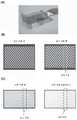
도 18은 제작 중의 발광 장치를 나타낸 사진.
도 19의 (A)~(C)는 터치 패널의 일례를 도시한 것.
도 20의 (A) 및 (B)는 터치 패널의 일례를 도시한 것.
도 21의 (A)~(C)는 터치 패널의 예를 도시한 것.
도 22의 (A)~(C)는 터치 패널의 예를 도시한 것.
도 23의 (A)~(G)는 전자 장치 및 조명 장치의 예를 도시한 것.
도 24의 (A)~(I)는 전자 장치의 예를 도시한 것.
도 25의 (A)~(C)는 굴곡 시험에 대하여 도시한 사진 및 도면.
도 26은 굴곡 부분을 도시한 것.
도 27의 (A)~(C)는 굴곡 시험 및 보존 시험의 결과를 나타낸 것.
도 28의 (A)~(C)는 굴곡 시험 및 보존 시험의 결과를 나타낸 것.
도 29의 (A) 및 (B)는 굴곡 시험기의 사진.
도 30의 (A) 및 (B)는 각각 박리 시험에 사용한 기기 및 시료의 구조예를 도시한 것.
도 31의 (A) 및 (B)는 각각 TDS 분석의 결과 및 박리성 평가의 결과를 나타낸 것.
도 32의 (A) 및 (B)는 각각 TDS 분석의 결과 및 박리성 평가의 결과를 나타낸 것.
도 33은 박리성의 평가 결과를 나타낸 것.
도 34의 (A) 및 (B)는 각각 TDS 분석의 결과 및 박리성 평가의 결과를 나타낸 것.
도 35의 (A) 및 (B)는 각각 TDS 분석의 결과 및 박리성 평가의 결과를 나타낸 것.
도 36의 (A) 및 (B)는 각각 TDS 분석의 결과 및 박리성 평가의 결과를 나타낸 것.
도 37의 (A)~(D)는 발광 장치의 제작 방법을 도시한 것.1 (A) to 1 (F) show an example of a manufacturing method of a light emitting device.
2 (A) to 2 (E) show an example of a manufacturing method of a light emitting device.
3 (A) to 3 (D) show examples of light emitting devices.
4 (A) to 4 (E) show examples of light emitting devices.
5 (A) to 5 (E) show the peeling method.
6 (A) to 6 (D) show the peeling method.
7 (A), (B1), (B2), (B3), (B4), (B5) and (C) show the peeling method.
8 (A) to 8 (D) show the peeling method.
9 (A) to 9 (D) show the peeling method.
10 (A) to (D) show the peeling method.
11 (A) to (C) show the peeling method.
Figs. 12 (A) to 12 (I) show the planar shape of the release layer.
Figs. 13A to 13C show a manufacturing method of the light emitting device. Fig.
14 (A) to 14 (C) show a manufacturing method of a light emitting device.
Figs. 15A to 15C show a manufacturing method of a light-emitting device. Fig.
Figs. 16A to 16C show a manufacturing method of a light emitting device. Fig.
17 (A) and 17 (B) show a manufacturing method of a light emitting device.
18 is a photograph showing a light emitting device during fabrication.
19A to 19C show an example of a touch panel.
20A and 20B show an example of a touch panel.
Figs. 21A to 21C show examples of a touch panel. Fig.
22 (A) to 22 (C) show examples of a touch panel.
23 (A) to 23 (G) show examples of an electronic device and a lighting device.
24 (A) to (I) show examples of electronic devices.
25 (A) to 25 (C) are photographs and drawings showing the bending test.
Fig. 26 shows a bent portion. Fig.
Figures 27 (A) to 27 (C) show the results of the bending test and the preservation test.
Figures 28 (A) to 28 (C) show the results of the bending test and the preservation test.
29 (A) and 29 (B) are photographs of a bending test machine.
30 (A) and 30 (B) show structural examples of the equipment and the sample used in the peeling test, respectively.
31 (A) and 31 (B) show the results of the TDS analysis and the results of the peelability evaluation, respectively.
32 (A) and 32 (B) show the results of the TDS analysis and the results of the peelability evaluation, respectively.
33 shows the evaluation results of the peelability.
Figures 34 (A) and 34 (B) show the results of the TDS analysis and the results of the peelability evaluation, respectively.
35 (A) and 35 (B) show the results of the TDS analysis and the results of the peelability evaluation, respectively.
Figures 36 (A) and 36 (B) show the results of the TDS analysis and the results of the peelability evaluation, respectively.
37A to 37D show a manufacturing method of the light emitting device.
실시형태에 대하여 도면을 참조하여 자세히 설명하기로 한다. 다만, 본 발명은 아래의 설명에 한정되지 않으며, 본 발명의 취지 및 범위에서 벗어남이 없이 다양한 변경 및 수정이 이루어질 수 있다는 것은 당업자에 의하여 쉽게 이해된다. 따라서, 본 발명은 아래 실시형태의 내용에 한정되어 해석되어서는 안 된다.Embodiments will be described in detail with reference to the drawings. However, it is to be understood that the present invention is not limited to the following description, and that various changes and modifications can be made without departing from the spirit and scope of the present invention. Therefore, the present invention should not be construed as being limited to the contents of the embodiments below.
또한, 아래에서 설명되는 발명의 구조에서, 동일한 부분 또는 같은 기능을 갖는 부분은 상이한 도면에서 동일한 부호로 표시되고, 이러한 부분의 설명은 반복되지 않는다. 또한, 같은 기능을 갖는 부분에 동일한 해칭 패턴을 부여하고, 그 부분을 특별히 부호로 표시하지 않는 경우가 있다.Also, in the structure of the invention described below, parts having the same or the same function are denoted by the same symbols in different drawings, and description of these parts is not repeated. In addition, there is a case where the same hatching pattern is given to a portion having the same function, and the portion is not specifically indicated by a sign.
또한, 도면 등에 도시된 각 구조의 위치, 크기, 범위 등은 이해하기 쉽게 하기 위하여 정확하게 나타내어지지 않은 경우가 있다. 그러므로, 개시된 발명은 도면 등에 개시된 위치, 크기, 범위 등에 반드시 한정되지는 않는다.In addition, the position, size, range, etc. of each structure shown in the drawings and the like may not be accurately shown in order to facilitate understanding. Therefore, the disclosed invention is not necessarily limited to the position, size, range, etc. disclosed in the drawings and the like.
(실시형태 1)(Embodiment 1)
본 실시형태에서는, 본 발명의 일 실시형태의 발광 장치와 그 제작 방법에 대하여 도 1의 (A)~(F), 도 2의 (A)~(E), 도 3의 (A)~(D), 및 도 4의 (A)~(E)를 참조하여 설명하기로 한다.1 (A) to 2 (F), 2 (A) to 2 (E) and 3 (A) to 3 (E) show a light emitting device and a manufacturing method thereof according to an embodiment of the present invention, D), and Figs. 4A to 4E.
제작 기판 위에 피박리층을 형성하고, 제작 기판으로부터 박리하고 나서, 다른 기판으로 이동시킬 수 있다. 이 방법을 이용하면, 예를 들어 내열성이 높은 제작 기판 위에서 형성한 피박리층을 내열성이 낮은 기판으로 이동할 수 있다. 그러므로, 피박리층의 제작 온도는 내열성이 낮은 기판에 의하여 제한되지 않는다. 또한, 제작 기판보다 가볍거나 얇거나 또는 가요성이 높은 기판 등에 피박리층을 이동시킬 수 있기 때문에, 반도체 장치, 발광 장치, 또는 표시 장치 등 다양한 장치를 가볍게, 얇게, 그리고 가요성 있게 할 수 있다.It is possible to form a layer to be peeled off on a substrate to be formed, to peel off the substrate to be formed, and then to move to another substrate. With this method, for example, the layer to be peeled formed on a substrate having high heat resistance can be moved to a substrate having low heat resistance. Therefore, the production temperature of the layer to be peeled is not limited by the substrate having low heat resistance. Further, since the layer to be peeled can be moved to a substrate that is lighter, thinner, or more flexible than a substrate to be formed, various devices such as a semiconductor device, a light emitting device, or a display device can be made light, thin, and flexible .
또한, 텔레비전 장치, 컴퓨터용 모니터, 디지털 카메라, 디지털 비디오 카메라, 디지털 포토 프레임, 휴대 전화, 휴대 게임기, 휴대 정보 단말기, 및 오디오 재생 장치 등의 다양한 장치를 포함한 전자 장치를 가볍게, 얇게, 그리고 가요성 있게 할 수 있다.In addition, electronic devices including various devices such as a television device, a computer monitor, a digital camera, a digital video camera, a digital photo frame, a mobile phone, a portable game machine, a portable information terminal, and an audio reproducing device can be lightly, thinly, You can do it.
본 발명의 일 실시형태에 의하여 제작할 수 있는 장치는 기능 소자를 포함한다. 기능 소자의 예에는, 트랜지스터 등의 반도체 소자; 발광 다이오드; 무기 EL 소자 및 유기 EL 소자 등의 발광 소자; 및 액정 소자 등의 표시 소자가 포함된다. 예를 들어, 트랜지스터를 포함한 반도체 장치 및 발광 소자를 포함한 발광 장치(여기서는, 트랜지스터 및 발광 소자를 포함한 표시 장치도 포함함)는 본 발명의 일 실시형태에 따라 제작할 수 있는 장치의 예이다.An apparatus which can be manufactured according to an embodiment of the present invention includes a functional element. Examples of functional devices include semiconductor devices such as transistors; Light emitting diodes; Light emitting elements such as inorganic EL elements and organic EL elements; And a display element such as a liquid crystal element. For example, a semiconductor device including a transistor and a light emitting device including a light emitting device (including a transistor and a display device including a light emitting device) are examples of devices that can be manufactured according to an embodiment of the present invention.
예를 들어, 유기 EL 소자는 수분 등으로 인하여 열화되기 쉬우므로, 방습성이 낮은 유기 수지 기판 위에 유기 EL 소자를 형성하면 신뢰성이 불충분한 경우가 있다. 여기서, 본 발명의 일 실시형태에 따르면, 방습성이 뛰어난 보호막을 유리 기판 위에 고온으로 형성함으로써, 이 보호막을 내열성 및 방습성이 낮은 가요성 유기 수지 기판으로 이동시킬 수 있다. 유기 수지 기판으로 이동한 보호막 위에 유기 EL 소자를 형성함으로써, 신뢰성이 높은 가요성 발광 장치를 제작할 수 있다.For example, since the organic EL device tends to deteriorate due to moisture or the like, reliability may be insufficient when the organic EL device is formed on the organic resin substrate having low humidity resistance. Here, according to one embodiment of the present invention, by forming a protective film having excellent moisture-proof property on a glass substrate at a high temperature, the protective film can be moved to a flexible organic resin substrate having low heat resistance and moisture resistance. By forming the organic EL element on the protective film moved to the organic resin substrate, a highly reliable flexible light emitting device can be manufactured.
다른 예로서는, 방습성이 뛰어난 보호막을 유리 기판 위에 고온으로 형성하고, 보호막 위에 유기 EL 소자를 형성한 후, 보호막 및 유기 EL 소자를 유리 기판으로부터 박리하고, 이 보호막을 내열성 및 방습성이 낮은 가요성 유기 수지 기판으로 이동시킬 수 있다. 유기 수지 기판에 보호막 및 유기 EL 소자를 이동시킴으로써, 신뢰성이 높은 가요성 발광 장치를 제작할 수 있다.As another example, a protective film having excellent moisture-proof property is formed on a glass substrate at a high temperature, an organic EL device is formed on the protective film, the protective film and the organic EL device are peeled off from the glass substrate and the protective film is laminated on the flexible organic resin Can be moved to the substrate. By moving the protective film and the organic EL element on the organic resin substrate, a highly reliable flexible light emitting device can be manufactured.
여기서는, 간단히 장치의 제작 방법을 2가지 설명한다. 또한, 본 실시형태에 있어서는, 실시형태 2에서 설명하는 장치의 제작 방법을 적절히 참조할 수 있다.Here, two methods of manufacturing the apparatus will be briefly described. In the present embodiment, the method of manufacturing the apparatus described in
도 1의 (A)~(F)에, 박리 공정을 한 번 수행하는 장치의 제작 방법을 도시하였다.1 (A) to 1 (F) show a manufacturing method of an apparatus for performing the peeling step once.
우선, 도 1의 (A)에 도시된 바와 같이, 제작 기판(101) 위에 박리층(103)을 개재(介在)하여 절연층(104)(예를 들어, 상술한 방습성이 뛰어난 보호막)을 형성한다. 필요하면, 절연층(104) 위에 소자층(106)(예를 들어, 상술한 유기 EL 소자 및 트랜지스터 등의 반도체 소자)의 적어도 일부를 더 형성한다. 그리고, 접착층(107)에 의하여 소자층(106)과 기판(109)을 서로 접합시킨다. 또한, 소자층(106)은 기판(109)과 접합시키기 전에 부분적으로 또는 전체적으로 형성하여도 좋고, 기판(114)에 절연층(104)을 이동시킨 후에 절연층(104) 위에 형성하여도 좋다.First, as shown in Fig. 1A, an insulating layer 104 (for example, a protective film excellent in the above-mentioned moisture-proof property) is formed by interposing a
다음에, 도 1의 (B)에 도시된 바와 같이, 박리층(103)을 이용하여 제작 기판(101)을 절연층(104)으로부터 박리한다.Next, as shown in Fig. 1 (B), the
그리고, 도 1의 (C)에 도시된 바와 같이, 노출된 절연층(104)을 접착층(112)에 의하여 기판(114)에 접합한다.1 (C), the exposed insulating
그 후, 접착층(107)을 용해 또는 가소화시킴으로써 기판(109)을 제거한다(도 1의 (D)). 도 1의 (E)에 있어서, 소자층(106)의 층들을 부분적으로 또는 전체적으로 형성할 필요가 있는 경우에는, 소자층(106)을 부분적으로 또는 전체적으로 형성한다. 예를 들어, 도 1의 (A)의 스텝에서 유기 EL 소자의 하부 전극까지의 요소를 형성하고, 도 1의 (E)의 스텝에서 상기 하부 전극 위에 EL층 및 상부 전극을 형성하여 유기 EL 소자를 완성시키는 구조를 적용하여도 좋다. 도 1의 (F)에 도시된 바와 같이, 소자층(106)의 형성 후에는 소자층(106)과 기판(173)을 접착층(171)에 의하여 서로 접합시킨다. 상술한 바와 같이 하여 본 발명의 일 실시형태의 장치를 제작할 수 있다.Thereafter, the
도 2의 (A)~(E)에, 박리 공정을 두 번 수행하는 장치의 제작 방법을 도시하였다.2 (A) to 2 (E) show a method of manufacturing an apparatus for performing the peeling step twice.
우선, 제작 기판(201) 위에 박리층(203)을 개재하여 절연층(204)(예를 들어, 상술한 방습성이 뛰어난 보호막)을 형성한다. 절연층(204) 위에 소자층(206)(예를 들어, 상술한 트랜지스터 등의 반도체 소자 및 유기 EL 소자 등의 소자를 포함하는 층)을 더 형성한다. 또한, 제작 기판(221) 위에 박리층(223)을 개재하여 절연층(224)(예를 들어, 상술한 방습성이 뛰어난 보호막)을 형성한다. 또한, 절연층(224) 위에 기능층(226)(예를 들어, 착색층, 차광층 등을 포함하며, 상술한 트랜지스터 등의 반도체 소자 및 유기 EL 소자 등의 소자를 포함하여도 좋은 층)을 형성한다. 그리고, 2개의 제작 기판의, 박리층이 각각 형성된 측의 면을 대향시켜, 접착층(207)에 의하여 소자층(206)과 기능층(226)을 접합시킨다(도 2의 (A)).First, an insulating layer 204 (for example, a protective film having excellent moisture and moisture resistance) is formed on a fabricated
다음에, 도 2의 (B)에 도시된 바와 같이, 박리층(203)을 이용하여 제작 기판(201)을 절연층(204)으로부터 박리한다. 그리고, 도 2의 (C)에 도시된 바와 같이, 노출된 절연층(204)과 기판(231)을 접착층(233)에 의하여 접합시킨다.Next, as shown in Fig. 2 (B), the
다음에, 도 2의 (D)에 도시된 바와 같이, 박리층(223)을 이용하여 제작 기판(221)을 절연층(224)으로부터 박리한다. 그리고, 도 2의 (E)에 도시된 바와 같이, 노출된 절연층(224)과 기판(173)을 접착층(171)에 의하여 접합시킨다. 상술한 바와 같이 하여, 본 발명의 일 실시형태의 장치를 제작할 수 있다.Next, as shown in FIG. 2D, the
장치를 제작하는 상술한 2가지의 방법에서, 제작 기판을 박리할 때 절연층, 소자층, 및 기능층의 막들(대표적으로는 무기 절연막)에 크랙(층 또는 막이 깨지거나 금이 가는 것)이 발생되는 경우가 있다. 박리할 때 발생된 크랙이 치명적이지 않더라도, 그 후의 제작 스텝(예를 들어, 가열 처리), 제작 후의 장치의 사용 등에 따라서는 크랙의 개수 또는 그 크기가 증대되는 경우가 있다. 장치 내에서의 크랙의 발생은, 소자의 오동작, 수명 저하 등을 초래하여, 장치의 신뢰성을 저하시키는 경우가 있다.In the above two methods for manufacturing the device, cracks (cracks or cracks in the layer or the film) on the insulating layer, the element layer, and the films of the functional layer (representatively, the inorganic insulating film) May occur. The number of cracks or the size thereof may be increased depending on the subsequent manufacturing steps (for example, heat treatment), the use of the apparatus after the production, and the like, even if the cracks generated during peeling are not fatal. Occurrence of cracks in the device may cause malfunction of the device, deterioration of its life, and the like, thereby lowering the reliability of the device.
그러므로 본 발명의 일 실시형태에 따르면, 장치에 사용하는 접착층의 경도를 쇼어 D 70보다 높게 설정한다. 따라서, 제작 기판의 박리 시에 절연층, 소자층, 및 기능층의 막들(대표적으로는 무기 절연막)에 크랙이 발생되는 것을 억제할 수 있다. 또한, 이 구조가 적용된 가요성 장치는 반복적인 굴곡에 대한 내성이 높으므로 바람직하다. 예를 들어, 본 발명의 일 실시형태의 장치는 굴곡될 때 0.1mm 이상 150mm 이하, 바람직하게는 1mm 이상 100mm 이하, 더 바람직하게는 1mm 이상 50mm 이하, 더욱 바람직하게는 2mm 이상 5mm 이하의 최소 곡률 반경을 가질 수 있다.Therefore, according to one embodiment of the present invention, the hardness of the adhesive layer used in the apparatus is set to be higher than the Shore D 70. Therefore, it is possible to suppress the occurrence of cracks in the insulating layer, the element layer, and the films of the functional layer (typically, the inorganic insulating film) at the time of peeling off the substrate to be produced. Further, the flexible device to which this structure is applied is preferable because it is highly resistant to repeated bending. For example, the apparatus of one embodiment of the present invention has a minimum curvature of not less than 0.1 mm and not more than 150 mm, preferably not less than 1 mm and not more than 100 mm, more preferably not less than 1 mm and not more than 50 mm, You can have a radius.
예를 들어, 상술한 접착층(107, 112, 171, 207, 및 233) 중 적어도 어느 하나에, 경도가 쇼어 D 70보다 높은 접착층을 사용하여도 좋다. 각 접착층의 경도가 쇼어 D 70보다 높은 것이 바람직하다.For example, an adhesive layer having a hardness higher than that of Shore D 70 may be used for at least one of the
또는, 본 발명의 일 실시형태에 따르면, 장치에 사용하는 가요성 기판의 팽창 계수가 58ppm/℃ 미만이다. 따라서, 절연층, 소자층, 기능층 등을 가요성 기판으로 이동시킨 후, 이들 층에서 크랙이 발생되거나 크랙이 성장하는 것을 억제할 수 있다.Alternatively, according to an embodiment of the present invention, the expansion coefficient of the flexible substrate used in the apparatus is less than 58 ppm / 占 폚. Therefore, after the insulating layer, the element layer, the functional layer, and the like are transferred to the flexible substrate, it is possible to suppress cracks or cracks from growing in these layers.
예를 들어, 상술한 기판(114, 173, 및 231) 중 적어도 어느 하나에 팽창 계수가 58ppm/℃ 미만인 기판을 사용하여도 좋다. 각 기판의 팽창 계수가 58ppm/℃ 미만인 것이 바람직하다.For example, a substrate having an expansion coefficient of less than 58 ppm / 占 폚 may be used for at least one of the
구체적으로는, 본 발명의 일 실시형태의 발광 장치는, 제 1 가요성 기판; 제 2 가요성 기판; 제 1 가요성 기판과 제 2 가요성 기판 사이의 소자층; 제 1 가요성 기판과 소자층 사이의 절연층; 제 1 가요성 기판과 절연층 사이의 제 1 접착층; 및 제 2 가요성 기판과 소자층 사이의 제 2 접착층을 포함한다. 소자층은 발광 소자를 포함한다.Specifically, the light emitting device of one embodiment of the present invention includes: a first flexible substrate; A second flexible substrate; An element layer between the first flexible substrate and the second flexible substrate; An insulating layer between the first flexible substrate and the element layer; A first adhesive layer between the first flexible substrate and the insulating layer; And a second adhesive layer between the second flexible substrate and the element layer. The element layer includes a light emitting element.
본 발명의 일 실시형태에 있어서, 제 1 접착층의 경도가 쇼어 D 70보다 높은 것이 바람직하고, 쇼어 D 80 이상인 것이 더 바람직하다.In one embodiment of the present invention, the hardness of the first adhesive layer is preferably higher than Shore D 70, and more preferably Shore D 80 or higher.
마찬가지로, 본 발명의 일 실시형태에 있어서, 제 2 접착층의 경도가 쇼어 D 70보다 높은 것이 바람직하고, 쇼어 D 80 이상인 것이 더 바람직하다.Likewise, in one embodiment of the present invention, the hardness of the second adhesive layer is preferably higher than Shore D 70, and more preferably Shore D 80 or higher.
본 발명의 일 실시형태에서는 제 1 접착층 및 제 2 접착층 양쪽의 경도가 쇼어 D 70보다 높은 것이 바람직하고, 쇼어 D 80 이상인 것이 더 바람직하지만, 본 발명의 일 실시형태는 이에 한정되지 않는다. 제 1 접착층 및 제 2 접착층의 한쪽의 경도가 쇼어 D 70보다 높아도 좋다. 또는, 예를 들어 크랙이 발생되기 쉬운 층을 소자층 또는 절연층에 사용하지 않는 경우에는, 제 1 접착층 및 제 2 접착층 양쪽의 경도가 쇼어 D 70 이하이어도 좋다.In one embodiment of the present invention, it is preferable that the hardness of both the first adhesive layer and the second adhesive layer is higher than Shore D 70, and more preferably Shore D 80 or higher. However, one embodiment of the present invention is not limited thereto. The hardness of one of the first adhesive layer and the second adhesive layer may be higher than that of Shore D70. Alternatively, for example, in the case where a layer that is susceptible to cracks is not used for the element layer or the insulating layer, the hardness of both the first adhesive layer and the second adhesive layer may be Shore D 70 or less.
본 발명의 일 실시형태에서는 제 1 가요성 기판의 팽창 계수가 58ppm/℃ 미만인 것이 바람직하고, 30ppm/℃ 이하인 것이 더 바람직하다.In one embodiment of the present invention, the expansion coefficient of the first flexible substrate is preferably less than 58 ppm / ° C, more preferably 30 ppm / ° C or less.
마찬가지로, 본 발명의 일 실시형태에서는 제 2 가요성 기판의 팽창 계수가 58ppm/℃ 미만인 것이 바람직하고, 30ppm/℃ 이하인 것이 더 바람직하다.Likewise, in one embodiment of the present invention, the coefficient of expansion of the second flexible substrate is preferably less than 58 ppm / 占 폚, more preferably 30 ppm / 占 폚 or less.
본 발명의 일 실시형태에서는, 제 1 가요성 기판 및 제 2 가요성 기판 양쪽의 팽창 계수가 58ppm/℃ 미만인 것이 바람직하고, 30ppm/℃ 이하인 것이 더 바람직하지만, 본 발명의 일 실시형태는 이에 한정되지 않는다. 제 1 가요성 기판 및 제 2 가요성 기판 중 한쪽의 팽창 계수가 58ppm/℃ 미만이어도 좋다. 또는, 예를 들어 크랙이 발생되기 쉬운 층을 소자층 또는 절연층에 사용하지 않는 경우에는, 제 1 가요성 기판 및 제 2 가요성 기판 양쪽의 팽창 계수가 58ppm/℃ 이상이어도 좋다.In one embodiment of the present invention, the expansion coefficient of both the first flexible substrate and the second flexible substrate is preferably less than 58 ppm / 占 폚, more preferably not more than 30 ppm / 占 폚. However, It does not. The expansion coefficient of one of the first flexible substrate and the second flexible substrate may be less than 58 ppm / 占 폚. Alternatively, for example, in the case where a layer susceptible to cracking is not used for the element layer or the insulating layer, the expansion coefficient of both the first flexible substrate and the second flexible substrate may be 58 ppm / ° C or higher.
아래에서는 본 발명의 일 실시형태가 적용된 발광 소자를 사용한 발광 장치의 구체적인 예에 대하여 설명한다.A specific example of a light emitting device using a light emitting element to which an embodiment of the present invention is applied will be described below.
<구체적인 예 1><Specific Example 1>
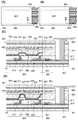
도 3의 (A)는 발광 장치의 평면도이고, 도 3의 (C)는 도 3의 (A)에서의 일점쇄선 A1-A2를 따른 단면도의 일례이다. 구체적인 예 1의 발광 장치는 컬러 필터 방식을 이용한 톱 이미션 발광 장치이다. 본 실시형태에서, 발광 장치는 예를 들어 적색(R), 녹색(G), 및 청색(B)의 3색의 부화소가 하나의 색을 표현하는 구조, R, G, B, 및 백색(W)의 4색의 부화소가 하나의 색을 표현하는 구조 등을 가질 수 있다. 색 요소는 특별히 한정되지 않으며, R, G, B, 및 W 이외의 색을 사용하여도 좋다. 예를 들어, 황색, 시안, 마젠타 등을 사용하여도 좋다.3 (A) is a plan view of the light emitting device, and FIG. 3 (C) is an example of a cross-sectional view along one-dot chain line A1-A2 in FIG. The light emitting device of specific example 1 is a top emission light emitting device using a color filter method. In the present embodiment, the light emitting device has a structure in which three color subpixels of red (R), green (G), and blue (B) represent one color, and R, G, B, and white W) of four colors may represent a single color. The color elements are not particularly limited, and colors other than R, G, B, and W may be used. For example, yellow, cyan, magenta, or the like may be used.
도 3의 (A)에 도시된 발광 장치는 발광부(804), 구동 회로부(806), 및 FPC(flexible printed circuit)(808)를 포함한다. 발광부(804) 및 구동 회로부(806)에 포함된 발광 소자 및 트랜지스터는 기판(801), 기판(803), 및 접착층(823)으로 밀봉된다.The light emitting device shown in FIG. 3A includes a
도 3의 (C)의 발광 장치는 기판(801), 접착층(811), 절연층(813), 복수의 트랜지스터, 도전층(857), 절연층(815), 절연층(817), 복수의 발광 소자, 절연층(821), 접착층(823), 오버코트(849), 착색층(845), 차광층(847), 절연층(843), 접착층(841), 및 기판(803)을 포함한다. 접착층(823), 오버코트(849), 절연층(843), 접착층(841), 및 기판(803)은 가시광을 투과시킨다.The light emitting device of FIG. 3C includes a
발광부(804)는 기판(801) 위에 접착층(811) 및 절연층(813)을 개재하여 트랜지스터(820) 및 발광 소자(830)를 포함한다. 발광 소자(830)는 절연층(817) 위에 하부 전극(831), 하부 전극(831) 위에 EL층(833), 및 EL층(833) 위에 상부 전극(835)을 포함한다. 하부 전극(831)은 트랜지스터(820)의 소스 전극 또는 드레인 전극에 전기적으로 접속된다. 하부 전극(831)의 단부는 절연층(821)으로 덮여 있다. 하부 전극(831)은 가시광을 반사하는 것이 바람직하다. 상부 전극(835)은 가시광을 투과시킨다.The
또한, 발광부(804)는 발광 소자(830)와 겹친 착색층(845), 및 절연층(821)과 겹친 차광층(847)을 포함한다. 착색층(845) 및 차광층(847)은 오버코트(849)로 덮여 있다. 발광 소자(830)와 오버코트(849) 사이의 공간은 접착층(823)으로 충전된다.The
절연층(815)은 트랜지스터에 포함되는 반도체로 불순물이 확산되는 것을 억제하는 효과를 갖는다. 절연층(817)으로서는, 트랜지스터로 인한 표면 요철을 저감시키기 위하여 평탄화 기능을 갖는 절연층을 선택하는 것이 바람직하다.The insulating
구동 회로부(806)는 기판(801) 위에 접착층(811) 및 절연층(813)을 개재하여 복수의 트랜지스터를 포함한다. 도 3의 (C)에는 구동 회로부(806)에 포함되는 하나의 트랜지스터를 도시하였다.The driving
절연층(813)과 기판(801)은 접착층(811)에 의하여 서로 접합된다. 절연층(843)과 기판(803)은 접착층(841)에 의하여 서로 접합된다. 절연층(813) 및 절연층(843)으로서 방습성이 뛰어난 막을 사용하면, 발광 소자(830) 또는 트랜지스터(820)에 수분 등 불순물이 들어가는 것을 억제할 수 있어, 발광 장치의 신뢰성 향상으로 이어지며, 바람직하다.The insulating
도전층(857)은 외부로부터의 신호(예를 들어, 비디오 신호, 클록 신호, 스타트 신호, 리셋 신호 등) 또는 전위를 구동 회로부(806)로 전달하기 위한 외부 입력 단자에 전기적으로 접속된다. 여기서는, 외부 입력 단자로서 FPC(808)가 제공되는 예에 대하여 설명한다. 제작 스텝 수의 증가를 방지하기 위하여 도전층(857)은 발광부 또는 구동 회로부에서의 전극 또는 배선과 동일한 재료 및 동일한 스텝을 사용하여 형성되는 것이 바람직하다. 여기서는 트랜지스터(820)의 전극과 동일한 재료 및 동일한 스텝을 사용하여 도전층(857)을 형성하는 예에 대하여 설명한다.The
도 3의 (C)의 발광 장치에서는, FPC(808)가 기판(803) 위에 위치한다. 기판(803), 접착층(841), 절연층(843), 접착층(823), 절연층(817), 및 절연층(815)에 제공된 개구를 통하여 접속체(825)가 도전층(857)에 접속된다. 또한, 접속체(825)는 FPC(808)에 접속된다. FPC(808)와 도전층(857)은 접속체(825)를 개재하여 서로 전기적으로 접속된다. 도전층(857)과 기판(803)이 서로 겹치는 경우에는, 기판(803)에 개구를 형성함으로써(또는 개구를 갖는 기판을 사용함으로써), 도전층(857), 접속체(825), 및 FPC(808)를 서로 전기적으로 접속시킨다.In the light emitting device of Fig. 3C, the
구체적인 예 1에 있어서, 접착층(811, 841, 및 823) 중 적어도 어느 하나에 경도가 쇼어 D 70보다 높은 접착층을 적용하는 것이 바람직하다. 접착층(811, 841, 및 823)의 각각에, 경도가 쇼어 D 70보다 높은 접착층을 적용하는 것이 특히 바람직하다. 그렇게 하면, 발광 장치의 제작 시에 절연층(813), 절연층(843), 트랜지스터, 발광 소자 등에 크랙이 발생되는 것을 억제할 수 있다. 또한, 상기 발광 장치는 반복적인 굴곡에 대한 높은 내성을 가질 수 있다.In concrete example 1, it is preferable to apply an adhesive layer having hardness higher than Shore D 70 to at least one of the
또한, 구체적인 예 1에서, 팽창 계수 58ppm/℃ 미만의 기판을, 바람직하게는 기판(801) 및 기판(803) 중 적어도 한쪽에 사용, 더 바람직하게는 이들 기판 양쪽에 사용한다. 그렇게 하면, 기판(801) 및 기판(803)으로 이동되는 절연층(813), 절연층(843), 트랜지스터, 발광 소자 등에서 크랙이 발생되는 것 또는 크랙이 성장하는 것을 억제할 수 있다. 또한, 상기 발광 장치는 반복적인 굴곡에 대한 높은 내성을 가질 수 있다.Further, in the specific example 1, a substrate having an expansion coefficient of less than 58 ppm / DEG C is preferably used for at least one of the
<구체적인 예 2><Specific Example 2>
도 3의 (B)는 발광 장치의 평면도이고, 도 3의 (D)는 도 3의 (B)에서의 일점쇄선 A3-A4를 따른 단면도의 일례이다. 구체적인 예 2의 발광 장치는, 구체적인 예 1의 발광 장치와 다른, 컬러 필터 방식을 이용한 톱 이미션 발광 장치이다. 여기서는, 구체적인 예 1과 다른 점만 설명하고, 구체적인 예 1과 동일한 점의 설명은 생략한다.Fig. 3B is a plan view of the light emitting device, and Fig. 3D is an example of a cross-sectional view along one-dot chain line A3-A4 in Fig. 3B. The light emitting device of the second specific example is a top emission light emitting device using a color filter method which is different from the light emitting device of the first specific example. Here, only points different from the concrete example 1 will be described, and description of the same points as in the specific example 1 will be omitted.
도 3의 (D)에 도시된 발광 장치는, 도 3의 (C)의 발광 장치와 다음 점에서 다르다.The light emitting device shown in FIG. 3 (D) differs from the light emitting device shown in FIG. 3 (C) in the following points.
도 3의 (D)의 발광 장치는 절연층(821) 위에 스페이서(827)를 포함한다. 스페이서(827)는 기판(801)과 기판(803) 사이의 거리를 조정할 수 있다.The light emitting device of FIG. 3 (D) includes a
또한, 도 3의 (D)의 발광 장치에서, 기판(801)은 기판(803)과 크기가 다르다. FPC(808)는 절연층(843) 위에 위치하고, 기판(803)과 겹치지 않는다. 접속체(825)는 절연층(843), 접착층(823), 절연층(817), 및 절연층(815)에 제공된 개구를 통하여 도전층(857)과 접속된다. 기판(803)에 개구를 형성할 필요가 없기 때문에, 기판(803)의 재료가 제한되지 않는다.Further, in the light emitting device of FIG. 3 (D), the
<구체적인 예 3><Specific Example 3>
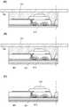
도 4의 (A)는 발광 장치의 평면도이고, 도 4의 (C)는 도 4의 (A)에서의 일점쇄선 A5-A6을 따른 단면도의 일례이다. 구체적인 예 3의 발광 장치는 독립 화소 방식(separate coloring method)을 이용한 톱 이미션 발광 장치이다.4 (A) is a plan view of the light emitting device, and FIG. 4 (C) is an example of a cross-sectional view along one-dot chain line A5-A6 in FIG. The light emitting device of Example 3 is a top emission light emitting device using a separate coloring method.
도 4의 (A)에 도시된 발광 장치는 발광부(804), 구동 회로부(806), 및 FPC(808)를 포함한다. 발광부(804) 및 구동 회로부(806)에 포함되는 발광 소자 및 트랜지스터는 기판(801), 기판(803), 틀 형태의 접착층(824), 및 접착층(823)으로 밀봉된다.The light emitting device shown in Fig. 4A includes a
도 4의 (C)의 발광 장치는 기판(801), 접착층(811), 절연층(813), 복수의 트랜지스터, 도전층(857), 절연층(815), 절연층(817), 복수의 발광 소자, 절연층(821), 접착층(823), 틀 형태의 접착층(824), 및 기판(803)을 포함한다. 접착층(823) 및 기판(803)은 가시광을 투과시킨다.The light emitting device of Figure 4C includes a
틀 형태의 접착층(824)은 접착층(823)보다 방습성이 좋은 것이 바람직하다. 그렇게 하면, 외부로부터 수분 등 불순물이 발광 장치로 들어가는 것을 억제할 수 있다. 그러므로, 상기 발광 장치의 신뢰성을 높일 수 있다.The frame-shaped
구체적인 예 3에서는, 발광 소자(830)로부터 방출된 광이 접착층(823)을 통하여 발광 장치로부터 추출된다. 이 이유로, 접착층(823)은 틀 형태의 접착층(824)보다 뛰어난 투광성을 갖는 것이 바람직하다. 또한, 접착층(823)은 틀 형태의 접착층(824)보다 높은 굴절률을 갖는 것이 바람직하다. 또한, 접착층(823)의 체적은 틀 형태의 접착층(824)보다 경화에 의하여 덜 수축되는 것이 바람직하다.In the specific example 3, the light emitted from the
발광부(804)는 기판(801) 위에 접착층(811) 및 절연층(813)을 개재하여 트랜지스터(820) 및 발광 소자(830)를 포함한다. 발광 소자(830)는 절연층(817) 위에 하부 전극(831), 하부 전극(831) 위에 EL층(833), 및 EL층(833) 위에 상부 전극(835)을 포함한다. 하부 전극(831)은 트랜지스터(820)의 소스 전극 또는 드레인 전극에 전기적으로 접속된다. 하부 전극(831)의 단부는 절연층(821)으로 덮여 있다. 하부 전극(831)은 가시광을 반사하는 것이 바람직하다. 상부 전극(835)은 가시광을 투과시킨다.The
구동 회로부(806)는 기판(801) 위에 접착층(811) 및 절연층(813)을 개재하여 복수의 트랜지스터를 포함한다. 도 4의 (C)에는 구동 회로부(806)에 포함되는 트랜지스터 중 하나를 도시하였다.The driving
절연층(813)과 기판(801)은 접착층(811)에 의하여 서로 접합된다. 절연층(813)에 방습성이 뛰어난 막을 사용하면, 발광 소자(830) 또는 트랜지스터(820)에 수분 등 불순물이 들어가는 것을 억제할 수 있어, 발광 장치의 신뢰성 향상으로 이어지며, 바람직하다.The insulating
도전층(857)은 외부로부터의 신호 또는 전위를 구동 회로부(806)로 전달하기 위한 외부 입력 단자에 전기적으로 접속된다. 여기서는, 외부 입력 단자로서 FPC(808)가 제공되는 예에 대하여 설명한다. 여기서는 트랜지스터(820)의 전극과 동일한 재료 및 동일한 스텝을 사용하여 도전층(857)을 형성하는 예에 대하여 설명한다.The
도 4의 (C)의 발광 장치에서는, FPC(808)가 기판(803) 위에 위치한다. 기판(803), 접착층(823), 절연층(817), 및 절연층(815)에 제공된 개구를 통하여 접속체(825)가 도전층(857)에 접속된다. 또한, 접속체(825)는 FPC(808)에 접속된다. FPC(808)와 도전층(857)은 접속체(825)를 개재하여 서로 전기적으로 접속된다.In the light emitting device of Fig. 4C, the
구체적인 예 3에서, 접착층(811 및 823) 중 적어도 한쪽, 더 바람직하게는 이들 접착층 양쪽에 경도가 쇼어 D 70보다 높은 접착층을 적용하는 것이 바람직하다. 그렇게 하면, 발광 장치의 제작 시에 절연층(813), 트랜지스터, 발광 소자 등에 크랙이 발생되는 것을 억제할 수 있다. 또한, 상기 발광 장치는 반복적인 굴곡에 대한 높은 내성을 가질 수 있다.In concrete example 3, it is preferable to apply at least one of the
또한, 구체적인 예 3에서, 팽창 계수 58ppm/℃ 미만의 기판을, 바람직하게는 기판(801) 및 기판(803) 중 적어도 한쪽에 사용, 더 바람직하게는 이들 기판 양쪽에 사용한다. 그렇게 하면, 기판(801)으로 이동시키는 절연층(813), 트랜지스터, 발광 소자 등에서 크랙이 발생되는 것 또는 크랙이 성장하는 것을 억제할 수 있다. 또한, 상기 발광 장치는 반복적인 굴곡에 대한 높은 내성을 가질 수 있다.Further, in the specific example 3, a substrate having an expansion coefficient of less than 58 ppm / 占 폚 is preferably used for at least one of the
<구체적인 예 4><Specific Example 4>
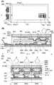
도 4의 (B)는 발광 장치의 평면도이고, 도 4의 (D)는 도 4의 (B)에서의 일점쇄선 A7-A8을 따른 단면도의 일례이다. 구체적인 예 4의 발광 장치는 컬러 필터 방식을 이용한 보텀 이미션 발광 장치이다.FIG. 4B is a plan view of the light emitting device, and FIG. 4D is an example of a cross-sectional view taken along one-dot chain line A7-A8 in FIG. 4B. The light emitting device of Example 4 is a bottom emission light emitting device using a color filter method.
도 4의 (D)의 발광 장치는 기판(801), 접착층(811), 절연층(813), 복수의 트랜지스터, 도전층(857), 절연층(815), 착색층(845), 절연층(817a), 절연층(817b), 도전층(816), 복수의 발광 소자, 절연층(821), 접착층(823), 및 기판(803)을 포함한다. 기판(801), 접착층(811), 절연층(813), 절연층(815), 절연층(817a), 및 절연층(817b)은 가시광을 투과시킨다.The light emitting device of Figure 4D includes a
발광부(804)는 기판(801) 위에 접착층(811) 및 절연층(813)을 개재하여 트랜지스터(820), 트랜지스터(822), 및 발광 소자(830)를 포함한다. 발광 소자(830)는 절연층(817) 위에 하부 전극(831), 하부 전극(831) 위에 EL층(833), 및 EL층(833) 위에 상부 전극(835)을 포함한다. 하부 전극(831)은 트랜지스터(820)의 소스 전극 또는 드레인 전극에 전기적으로 접속된다. 하부 전극(831)의 단부는 절연층(821)으로 덮여 있다. 상부 전극(835)은 가시광을 반사하는 것이 바람직하다. 하부 전극(831)은 가시광을 투과시킨다. 발광 소자(830)와 겹치는 착색층(845)의 위치는 특별히 한정되지 않으며, 예를 들어 절연층(817a)과 절연층(817b) 사이 또는 절연층(815)과 절연층(817a) 사이라도 좋다.The
구동 회로부(806)는 기판(801) 위에 접착층(811) 및 절연층(813)을 개재하여 복수의 트랜지스터를 포함한다. 도 4의 (C)에는 구동 회로부(806)에 포함되는 트랜지스터 중 2개를 도시하였다.The driving
절연층(813)과 기판(801)은 접착층(811)에 의하여 서로 접합된다. 절연층(813)에 방습성이 뛰어난 막을 사용하면, 발광 소자(830) 또는 트랜지스터(820 및 822)에 수분 등 불순물이 들어가는 것을 억제할 수 있어, 발광 장치의 신뢰성 향상으로 이어지며, 바람직하다.The insulating
도전층(857)은 외부로부터의 신호 또는 전위를 구동 회로부(806)로 전달하기 위한 외부 입력 단자에 전기적으로 접속된다. 여기서는, 외부 입력 단자로서 FPC(808)가 제공되는 예에 대하여 설명한다. 여기서는 도전층(816)과 동일한 재료 및 동일한 스텝을 사용하여 도전층(857)을 형성하는 예에 대하여 설명한다.The
구체적인 예 4에서, 접착층(811 및 823) 중 적어도 한쪽, 더 바람직하게는 이들 접착층 양쪽에 경도가 쇼어 D 70보다 높은 접착층을 적용하는 것이 바람직하다. 그렇게 하면, 발광 장치의 제작 시에 절연층(813), 트랜지스터, 발광 소자 등에 크랙이 발생되는 것을 억제할 수 있다. 또한, 상기 발광 장치는 반복적인 굴곡에 대한 높은 내성을 가질 수 있다.In concrete example 4, it is preferable to apply at least one of the
또한, 구체적인 예 4에서, 팽창 계수 58ppm/℃ 미만의 기판을, 바람직하게는 기판(801) 및 기판(803) 중 적어도 한쪽에 사용, 더 바람직하게는 이들 기판 양쪽에 사용한다. 그렇게 하면, 기판(801)으로 이동되는 절연층(813), 트랜지스터, 발광 소자 등에서 크랙이 발생되는 것 또는 크랙이 성장하는 것을 억제할 수 있다. 또한, 상기 발광 장치는 반복적인 굴곡에 대한 높은 내성을 가질 수 있다.Further, in Example 4, a substrate having an expansion coefficient of less than 58 ppm / 占 폚 is preferably used for at least one of the
<구체적인 예 5><Specific Example 5>
도 4의 (E)는 구체적인 예 1~4와 다른 발광 장치의 예를 나타낸 것이다.FIG. 4E shows an example of a light-emitting device different from the concrete examples 1 to 4.
도 4의 (E)의 발광 장치는 기판(801), 접착층(811), 절연층(813), 도전층(814), 도전층(857a), 도전층(857b), 발광 소자(830), 절연층(821), 접착층(823), 및 기판(803)을 포함한다.The light emitting device of Figure 4E includes a
도전층(857a) 및 도전층(857b)은 발광 장치의 외부 접속 전극이며, 각각 FPC 등에 전기적으로 접속될 수 있다.The
발광 소자(830)는 하부 전극(831), EL층(833), 및 상부 전극(835)을 포함한다. 하부 전극(831)의 단부는 절연층(821)으로 덮여 있다. 발광 소자(830)는 보텀 이미션 구조, 톱 이미션 구조, 또는 듀얼 이미션 구조를 갖는다. 각각 광이 추출되는 전극, 기판, 절연층 등은 가시광을 투과시킨다. 도전층(814)은 하부 전극(831)에 전기적으로 접속된다.The
광이 추출되는 기판은 광 추출 구조로서 반구(半球) 렌즈, 마이크로 렌즈 어레이, 요철 표면 구조가 제공된 필름, 광 확산 필름 등을 가져도 좋다. 예를 들어, 상기 기판 또는 렌즈 또는 필름과 실질적으로 동일한 굴절률을 갖는 접착제 등에 의하여 상술한 렌즈 또는 필름을 수지 기판에 접착함으로써 광 추출 구조를 갖는 기판을 형성할 수 있다.The substrate from which the light is extracted may have a hemispherical lens, a micro lens array, a film provided with a concavo-convex surface structure, a light diffusion film, or the like as the light extracting structure. For example, a substrate having a light extracting structure can be formed by adhering the above-described lens or film to a resin substrate by an adhesive having a refractive index substantially equal to that of the substrate or the lens or film.
도전층(814)은, 반드시 제공할 필요는 없지만, 하부 전극(831)의 저항으로 인한 전압 강하를 억제할 수 있기 때문에 제공하는 것이 바람직하다. 또한, 같은 의도로, 상부 전극(835)에 전기적으로 접속되는 도전층을 절연층(821), EL층(833), 또는 상부 전극(835) 등 위에 제공하여도 좋다.The
도전층(814)은 구리, 타이타늄, 탄탈럼, 텅스텐, 몰리브데넘, 크로뮴, 네오디뮴, 스칸듐, 니켈, 또는 알루미늄 중에서 선택된 재료, 또는 이들 재료 중 어느 것을 주성분으로 함유한 합금 재료를 사용한 단층 구조 또는 적층 구조를 가지도록 형성될 수 있다. 도전층(814)의 두께는, 예를 들어, 0.1μm 이상 3μm 이하, 바람직하게는 0.1μm 이상 0.5μm 이하로 할 수 있다.The
상부 전극(835)에 전기적으로 접속되는 도전층의 재료로서 페이스트(예를 들어, 은 페이스트)를 사용하면, 도전층을 형성하는 금속 입자가 응집되기 때문에, 도전층의 표면은 거칠고 많은 틈을 갖게 된다. 그러므로, 상기 도전층을 절연층(821) 위에 형성하여도, 예를 들어, EL층(833)이 도전층을 완전히 덮기 어렵기 때문에, 상부 전극과 도전층이 서로 전기적으로 접속되기 쉬워지며, 바람직하다.When a paste (for example, silver paste) is used as the material of the conductive layer electrically connected to the
구체적인 예 5에서, 접착층(811 및 823) 중 적어도 한쪽, 더 바람직하게는 이들 접착층 양쪽에 경도가 쇼어 D 70보다 높은 접착층을 적용하는 것이 바람직하다. 그렇게 하면, 발광 장치의 제작 시에 절연층(813), 발광 소자 등에 크랙이 발생되는 것을 억제할 수 있다. 또한, 상기 발광 장치는 반복적인 굴곡에 대한 높은 내성을 가질 수 있다.In concrete example 5, it is preferable to apply at least one of the
또한, 구체적인 예 5에서, 팽창 계수 58ppm/℃ 미만의 기판을, 바람직하게는 기판(801) 및 기판(803) 중 적어도 한쪽에 사용, 더 바람직하게는 이들 기판 양쪽에 사용한다. 그렇게 하면, 기판(801)으로 이동되는 절연층(813), 발광 소자 등에서 크랙이 발생되는 것 또는 크랙이 성장하는 것을 억제할 수 있다. 또한, 상기 발광 장치는 반복적인 굴곡에 대한 높은 내성을 가질 수 있다.Further, in the specific example 5, a substrate having an expansion coefficient of less than 58 ppm / 占 폚 is preferably used for at least one of the
<재료의 예><Examples of materials>
다음에, 발광 장치에 사용할 수 있는 재료 등에 대하여 설명한다. 다만, 본 명세서 등에서 이미 설명한 구성요소에 대한 설명은 생략하는 경우가 있다.Next, materials usable for the light emitting device will be described. However, the description of the components already described in this specification and the like may be omitted.
기판의 재료로서는, 유리, 석영, 유기 수지, 금속, 합금 등을 사용할 수 있다. 발광 소자로부터의 광을 추출하기 위한 기판은, 이 광을 투과시키는 재료를 사용하여 형성한다.As the material of the substrate, glass, quartz, organic resin, metal, alloy or the like can be used. A substrate for extracting light from the light emitting element is formed using a material that transmits the light.
특히, 가요성 기판을 사용하는 것이 바람직하다. 예를 들어, 유기 수지, 가요성을 가질 정도로 얇은 유리 재료, 금속, 또는 합금을 사용할 수 있다.In particular, it is preferable to use a flexible substrate. For example, an organic resin, a glass material thin enough to have flexibility, a metal, or an alloy may be used.
유기 수지는, 유리보다 비중이 작으며, 가요성 기판에 사용하는 것이 바람직하고, 이 경우 유리를 사용하는 경우에 비하여 발광 장치를 경량화시킬 수 있다.The organic resin has a specific gravity smaller than that of glass, and is preferably used in a flexible substrate. In this case, the light emitting device can be made lighter than in the case of using glass.
기판은 인성(toughness)이 강한 재료를 사용하여 형성하는 것이 바람직하다. 이 경우, 파손되기 어려운, 내충격성이 높은 발광 장치를 제공할 수 있다. 예를 들어, 유기 수지 기판 또는 얇은 금속 또는 합금 기판을 사용하면, 발광 장치를 유리 기판을 사용하는 경우에 비하여 가볍게, 그리고 파손되기 어렵게 할 수 있다.The substrate is preferably formed using a material having high toughness. In this case, it is possible to provide a light emitting device that is less prone to breakage and has high impact resistance. For example, when an organic resin substrate or a thin metal or alloy substrate is used, the light emitting device can be made light and hard to break as compared with the case of using a glass substrate.
금속 재료 및 합금 재료는, 열 전도성이 높으며, 기판 전체에 열을 쉽게 전도할 수 있기 때문에 발광 장치에서의 국소적인 온도 상승을 방지할 수 있으므로 바람직하다. 금속 재료 또는 합금 재료를 사용한 기판의 두께는 10μm 이상 200μm 이하인 것이 바람직하고, 20μm 이상 50μm 이하인 것이 더 바람직하다.The metal material and the alloy material are preferable because they have high thermal conductivity and can easily transmit heat to the entire substrate, thereby preventing a local temperature rise in the light emitting device. The thickness of the substrate using a metal material or an alloy material is preferably 10 占 퐉 or more and 200 占 퐉 or less, more preferably 20 占 퐉 or more and 50 占 퐉 or less.
금속 기판 또는 합금 기판의 재료에 특별한 한정은 없지만, 예를 들어 알루미늄, 구리, 니켈, 알루미늄 합금 또는 스테인리스강 등의 금속 합금을 사용하는 것이 바람직하다.The material of the metal substrate or the alloy substrate is not particularly limited, but it is preferable to use a metal alloy such as aluminum, copper, nickel, aluminum alloy, or stainless steel.
또한, 기판에 열 방사율이 높은 재료를 사용하면, 발광 장치의 표면 온도가 상승되는 것을 방지할 수 있어, 발광 장치의 파손 또는 신뢰성 저하의 방지로 이어진다. 예를 들어, 기판은 금속 기판과 열 방사율이 높은 층(이 층은 예를 들어, 금속 산화물 또는 세라믹 재료를 사용하여 형성할 수 있음)의 적층 구조를 가져도 좋다.In addition, if a material having a high thermal emissivity is used for the substrate, the surface temperature of the light emitting device can be prevented from rising, and the light emitting device can be prevented from being damaged or the reliability being lowered. For example, the substrate may have a laminate structure of a metal substrate and a layer having a high heat emissivity (this layer may be formed using, for example, a metal oxide or a ceramic material).
이와 같은 가요성 및 투광성을 갖는 재료의 예에는, 폴리에틸렌 테레프탈레이트(PET) 및 폴리에틸렌 나프탈레이트(PEN) 등의 폴리에스터 수지, 폴리아크릴로나이트릴 수지, 폴리이미드 수지, 폴리메틸 메타크릴레이트 수지, 폴리카보네이트(PC) 수지, 폴리에터설폰(PES) 수지, 폴리아마이드 수지, 사이클로올레핀 수지, 폴리스타이렌 수지, 폴리아마이드이미드 수지, 및 폴리염화바이닐 수지가 포함된다. 특히, 열팽창 계수가 낮은 재료가 바람직하며, 예를 들어 폴리아마이드이미드 수지, 폴리이미드 수지, PET 등을 적합하게 사용할 수 있다. 섬유체에 수지가 함침(含浸)된 기판(프리프레그라고도 함), 또는 무기 필러를 유기 수지와 혼합하여 열팽창 계수를 저감시킨 기판을 사용할 수도 있다.Examples of such flexible and translucent materials include polyester resins such as polyethylene terephthalate (PET) and polyethylene naphthalate (PEN), polyacrylonitrile resins, polyimide resins, polymethyl methacrylate resins, Polycarbonate (PC) resin, polyethersulfone (PES) resin, polyamide resin, cycloolefin resin, polystyrene resin, polyamideimide resin, and polyvinyl chloride resin. Particularly, a material having a low coefficient of thermal expansion is preferable, and for example, polyamideimide resin, polyimide resin, PET and the like can be suitably used. A substrate (also referred to as a prepreg) in which a resin is impregnated (impregnated) with a fibrous body, or a substrate in which an inorganic filler is mixed with an organic resin and a thermal expansion coefficient is reduced can be used.
가요성 기판은, 상술한 재료 중 어느 것의 층 위에, 발광 장치의 표면을 대미지로부터 보호하는 하드 코트층(질화 실리콘층 등), 압력을 분산할 수 있는 층(아라미드 수지층 등) 등이 적층되는 적층 구조이어도 좋다.On the flexible substrate, a hard coat layer (a silicon nitride layer or the like) for protecting the surface of the light emitting device from damage, a layer capable of dispersing pressure (an aramid resin layer or the like), and the like are laminated on any of the above- Or a laminated structure.
가요성 기판은 복수의 층을 적층하여 형성하여도 있다. 유리층을 사용하면, 물 및 산소에 대한 배리어성이 향상될 수 있어, 신뢰성이 높은 발광 장치를 제공할 수 있다.The flexible substrate may be formed by laminating a plurality of layers. When the glass layer is used, the barrier property to water and oxygen can be improved, and a highly reliable light emitting device can be provided.
예를 들어, 유기 EL 소자에 가까운 측으로부터 유리층, 접착층, 및 유기 수지층을 적층한 가요성 기판을 사용할 수 있다. 유리층의 두께는 20μm 이상 200μm 이하, 바람직하게는 25μm 이상 100μm 이하로 한다. 이러한 두께에 의하여, 유리층은 물 및 산소에 대한 높은 배리어성과 높은 가요성의 양쪽을 가질 수 있다. 유기 수지층의 두께는 10μm 이상 200μm 이하, 바람직하게는 20μm 이상 50μm 이하로 한다. 이러한 유기 수지층을 유리층의 외측에 제공함으로써, 유리층에서의 크랙 또는 깨짐의 발생을 억제하고 기계적 강도를 향상시킬 수 있다. 이러한 유리 재료와 유기 수지의 복합 재료를 포함하는 기판을 사용하여, 신뢰성이 높은 가요성 발광 장치를 제공할 수 있다.For example, a flexible substrate obtained by laminating a glass layer, an adhesive layer, and an organic resin layer from the side close to the organic EL element can be used. The thickness of the glass layer is not less than 20 μm and not more than 200 μm, preferably not less than 25 μm and not more than 100 μm. With this thickness, the glass layer can have both high barrier properties and high flexibility for water and oxygen. The thickness of the organic resin layer is 10 占 퐉 or more and 200 占 퐉 or less, preferably 20 占 퐉 or more and 50 占 퐉 or less. By providing such an organic resin layer on the outer side of the glass layer, occurrence of cracks or cracks in the glass layer can be suppressed and the mechanical strength can be improved. By using such a substrate including a composite material of a glass material and an organic resin, a highly reliable flexible light emitting device can be provided.
접착층으로서는, 자외선 경화성 접착제 등의 광 경화성 접착제, 반응 경화성 접착제, 열 경화성 접착제, 및 혐기성 접착제 등의 다양한 경화성 접착제를 사용할 수 있다. 이러한 접착제의 예에는, 에폭시 수지, 아크릴 수지, 실리콘(silicone) 수지, 페놀 수지, 폴리이미드 수지, 이미드 수지, 폴리바이닐 클로라이드(PVC) 수지, 폴리바이닐 뷰티랄(PVB) 수지, 에틸렌 바이닐 아세테이트(EVA) 수지 등이 포함된다. 특히 에폭시 수지 등 투습성이 낮은 재료를 사용하는 것이 바람직하다. 또는, 2성분 혼합형(two-component-mixture-type) 수지를 사용하여도 좋다. 또는, 접착 시트 등을 사용하여도 좋다.As the adhesive layer, various curable adhesives such as a photocurable adhesive such as an ultraviolet curable adhesive, a reactive curable adhesive, a thermosetting adhesive, and an anaerobic adhesive can be used. Examples of such adhesives include epoxy resin, acrylic resin, silicone resin, phenol resin, polyimide resin, imide resin, polyvinyl chloride (PVC) resin, polyvinyl butyral (PVB) resin, ethylene vinyl acetate EVA) resin and the like. Particularly, it is preferable to use a material having low moisture permeability such as an epoxy resin. Alternatively, a two-component-mixture-type resin may be used. Alternatively, an adhesive sheet or the like may be used.
또한, 상기 수지가 건조제를 포함하여도 좋다. 예를 들어, 알칼리 토금속의 산화물(예를 들어, 산화 칼슘 또는 산화 바륨) 등, 화학 흡착에 의하여 수분을 흡착하는 물질을 사용할 수 있다. 또는, 제올라이트 또는 실리카겔 등, 물리 흡착에 의하여 수분을 흡착하는 물질을 사용하여도 좋다. 건조제가 포함되면, 수분 등 불순물이 기능 소자로 들어가는 것을 억제할 수 있어 발광 장치의 신뢰성을 향상시킬 수 있으며, 바람직하다.Further, the resin may contain a drying agent. For example, a substance capable of adsorbing moisture by chemical adsorption such as an oxide of an alkaline earth metal (e.g., calcium oxide or barium oxide) can be used. Alternatively, a material capable of adsorbing moisture by physical adsorption such as zeolite or silica gel may be used. When the drying agent is contained, impurities such as moisture can be prevented from entering the functional device, thereby improving the reliability of the light emitting device.
또한, 상기 수지에 굴절률이 높은 필러 또는 광 산란 부재를 혼합하면, 발광 소자로부터의 광 추출 효율을 향상시킬 수 있다. 예를 들어, 산화 타이타늄, 산화 바륨, 제올라이트, 지르코늄 등을 사용할 수 있다.Further, when the resin is mixed with a filler or light scattering member having a high refractive index, light extraction efficiency from the light emitting element can be improved. For example, titanium oxide, barium oxide, zeolite, zirconium and the like can be used.
발광 장치의 트랜지스터의 구조에 특별한 한정은 없다. 예를 들어, 순 스태거(forward staggered) 트랜지스터로 하여도 좋고, 역 스태거(inverted staggered) 트랜지스터로 하여도 좋다. 또한, 톱 게이트 트랜지스터 또는 보텀 게이트 트랜지스터를 사용하여도 좋다. 트랜지스터에 사용되는 반도체 재료에 특별한 한정은 없으며, 예를 들어 실리콘, 저마늄 등을 사용할 수 있다. 또는, In-Ga-Zn계 금속 산화물 등 인듐, 갈륨, 및 아연 중 적어도 하나를 함유한 산화물 반도체를 사용하여도 좋다.There is no particular limitation on the structure of the transistor of the light emitting device. For example, the transistor may be a forward staggered transistor or an inverted staggered transistor. A top gate transistor or a bottom gate transistor may also be used. There is no particular limitation on the semiconductor material used for the transistor, and for example, silicon, germanium, or the like can be used. Alternatively, an oxide semiconductor containing at least one of indium, gallium, and zinc, such as an In-Ga-Zn based metal oxide, may be used.
트랜지스터에 사용하는 반도체 재료의 결정성에 특별한 한정은 없으며, 비정질 반도체 또는 결정성을 갖는 반도체(미결정 반도체, 다결정 반도체, 단결정 반도체, 또는 부분적으로 결정 영역을 포함하는 반도체)를 사용하여도 좋다. 결정성을 갖는 반도체를 사용하면, 트랜지스터 특성의 열화가 억제되며, 바람직하다.There is no particular limitation on the crystallinity of the semiconductor material used for the transistor, and an amorphous semiconductor or a semiconductor having crystallinity (a microcrystalline semiconductor, a polycrystalline semiconductor, a single crystal semiconductor, or a semiconductor partially including a crystal region) may be used. When a semiconductor having crystallinity is used, deterioration of transistor characteristics is suppressed, which is preferable.
트랜지스터의 안정적인 특성을 위하여 하지막을 제공하는 것이 바람직하다. 하지막은 산화 실리콘막, 질화 실리콘막, 산화질화 실리콘막, 또는 질화산화 실리콘막 등의 무기 절연막을 사용한 단층 구조 또는 적층 구조로 형성할 수 있다. 하지막은 스퍼터링법, 화학 기상 증착(CVD)법(예를 들어, 플라스마 CVD법, 열 CVD법, 또는 유기 금속 CVD(MOCVD)법), 원자층 증착(ALD)법, 도포법, 인쇄법 등에 의하여 형성할 수 있다. 또한, 하지막은 필요 없으면 제공할 필요는 없다. 상술한 구조예의 각각에서는, 절연층(813)이 트랜지스터의 하지막의 역할을 할 수 있다.It is preferable to provide a base film for stable characteristics of the transistor. The underlying film can be formed into a single layer structure or a laminated structure using an inorganic insulating film such as a silicon oxide film, a silicon nitride film, a silicon oxynitride film, or a silicon nitride oxide film. The underlying film may be formed by a sputtering method, a chemical vapor deposition (CVD) method (for example, a plasma CVD method, a thermal CVD method or an organic metal CVD (MOCVD) method), an atomic layer deposition (ALD) method, . Further, it is not necessary to provide the base film if it is unnecessary. In each of the above-described structural examples, the insulating
발광 소자로서는 자발광(self-luminous) 소자를 사용할 수 있고, 전류 또는 전압에 의하여 휘도가 제어되는 소자가 발광 소자의 범주에 포함된다. 예를 들어, 발광 다이오드(LED), 유기 EL 소자, 무기 EL 소자 등을 사용할 수 있다.As the light emitting element, a self-luminous element can be used, and a device whose luminance is controlled by current or voltage is included in the category of the light emitting element. For example, a light emitting diode (LED), an organic EL element, an inorganic EL element, or the like can be used.
발광 소자는 톱 이미션 구조, 보텀 이미션 구조, 및 듀얼 이미션 구조 중 어느 구조를 가져도 좋다. 광이 추출되는 전극으로서는 가시광을 투과시키는 도전막을 사용한다. 광이 추출되지 않는 전극으로서는 가시광을 반사하는 도전막을 사용하는 것이 바람직하다.The light emitting element may have any structure of a top emission structure, a bottom emission structure, and a dual emission structure. As the electrode from which light is extracted, a conductive film for transmitting visible light is used. As the electrode from which no light is extracted, it is preferable to use a conductive film which reflects visible light.
가시광을 투과시키는 도전막은, 예를 들어, 산화 인듐, 인듐 주석 산화물(ITO), 인듐 아연 산화물, 산화 아연, 또는 갈륨이 첨가된 산화 아연을 사용하여 형성할 수 있다. 또는, 금, 은, 백금, 마그네슘, 니켈, 텅스텐, 크로뮴, 몰리브데넘, 철, 코발트, 구리, 팔라듐, 또는 타이타늄 등의 금속 재료; 이들 금속 재료 중 어느 것을 함유하는 합금; 또는 이들 금속 재료 중 어느 것의 질화물(예를 들어, 질화 타이타늄) 등의 막을 투광성을 가질 정도로 얇게 형성할 수 있다. 또는, 상술한 재료 중 어느 것의 적층막을 도전막으로서 사용할 수 있다. 예를 들어, 은과 마그네슘의 합금과 ITO의 적층막을 사용하면, 도전성을 높일 수 있으며, 바람직하다. 또는, 그래핀 등을 사용하여도 좋다.The conductive film through which visible light is transmitted can be formed using, for example, indium oxide, indium tin oxide (ITO), indium zinc oxide, zinc oxide, or zinc oxide to which gallium is added. Or metal materials such as gold, silver, platinum, magnesium, nickel, tungsten, chromium, molybdenum, iron, cobalt, copper, palladium or titanium; An alloy containing any of these metal materials; Or a nitride of any of these metal materials (e.g., titanium nitride) can be formed thin enough to have translucency. Alternatively, a laminated film of any of the above materials may be used as the conductive film. For example, the use of an alloy of silver and magnesium and a laminate film of ITO can increase the conductivity, which is preferable. Alternatively, graphene or the like may be used.
가시광을 반사하는 도전막에는, 예를 들어, 알루미늄, 금, 백금, 은, 니켈, 텅스텐, 크로뮴, 몰리브데넘, 철, 코발트, 구리, 또는 팔라듐 등의 금속 재료, 또는 이들 금속 재료 중 어느 것을 함유하는 합금을 사용할 수 있다. 또한, 상기 금속 재료 또는 합금에 란타넘, 네오디뮴, 또는 저마늄 등이 첨가되어도 좋다. 또한, 알루미늄과 타이타늄의 합금, 알루미늄과 니켈의 합금, 또는 알루미늄과 네오디뮴의 합금 등 알루미늄을 함유한 합금(알루미늄 합금); 또는 은과 구리의 합금, 은, 팔라듐, 및 구리의 합금, 또는 은과 마그네슘의 합금 등을 함유한 합금을 도전막에 사용할 수 있다. 은과 구리의 합금은 내열성이 높으므로 바람직하다. 또한, 알루미늄 합금막 위에 이것과 접촉되는 금속막 또는 금속 산화물막을 적층하면, 알루미늄 합금막의 산화를 억제할 수 있다. 상기 금속막 또는 금속 산화물막의 재료의 예에는 타이타늄 및 산화 타이타늄이 포함된다. 또는, 상술한 가시광을 투과시키는 도전막과 금속 재료를 함유하는 막을 적층하여도 좋다. 예를 들어, 은과 ITO의 적층막, 또는 은과 마그네슘의 합금과 ITO의 적층막을 사용할 수 있다.As the conductive film for reflecting visible light, for example, a metal material such as aluminum, gold, platinum, silver, nickel, tungsten, chromium, molybdenum, iron, cobalt, copper or palladium, May be used. In addition, lanthanum, neodymium, or germanium may be added to the metal material or the alloy. Further, an alloy (aluminum alloy) containing aluminum such as an alloy of aluminum and titanium, an alloy of aluminum and nickel, or an alloy of aluminum and neodymium; Or an alloy of silver and copper, an alloy of silver, palladium, and copper, or an alloy of silver and magnesium, or the like may be used for the conductive film. Silver and copper alloys are preferred because they have high heat resistance. Furthermore, oxidation of the aluminum alloy film can be suppressed by laminating a metal film or a metal oxide film in contact with the aluminum alloy film. Examples of the material of the metal film or the metal oxide film include titanium and titanium oxide. Alternatively, a film containing a metal material and a conductive film for transmitting the visible light described above may be laminated. For example, a laminated film of silver and ITO, or an alloy of silver and magnesium and a laminated film of ITO can be used.
각 전극은 증착법 또는 스퍼터링법에 의하여 형성할 수 있다. 또는, 잉크젯법 등의 토출법(discharging method), 스크린 프린팅법 등의 인쇄법, 또는 도금법을 이용하여도 좋다.Each electrode can be formed by a vapor deposition method or a sputtering method. Alternatively, a printing method such as a discharging method such as an ink jet method or a screen printing method, or a plating method may be used.
하부 전극(831)과 상부 전극(835) 사이에 발광 소자의 문턱 전압보다 높은 전압을 인가하였을 때, 양극 측으로부터 EL층(833)으로 정공이 주입되고 음극 측으로부터 EL층(833)으로 전자가 주입된다. 주입된 전자와 정공은 EL층(833)에서 재결합되어, EL층(833)에 함유된 발광 물질이 발광한다.Holes are injected from the anode side to the
EL층(833)은 적어도 발광층을 포함한다. 발광층에 더하여, EL층(833)은 정공 주입성이 높은 물질, 정공 수송성이 높은 물질, 정공 블로킹 재료, 전자 수송성이 높은 물질, 전자 주입성이 높은 물질, 바이폴라(bipolar)성을 갖는 물질(전자 및 정공 수송성이 높은 물질) 등 중 어느 물질을 함유한 하나 이상의 층을 더 함유하여도 좋다.The
EL층(833)에는, 저분자 화합물 및 고분자 화합물 중 어느 쪽이나 사용할 수 있고, 무기 화합물을 사용하여도 좋다. EL층(833)에 포함되는 각 층은 증착법(진공 증착법을 포함함), 전사법(transfer method), 인쇄법, 잉크젯법, 도포법 등 중 어느 방법에 의하여 형성할 수 있다.In the
발광 소자는 방습성이 뛰어난 한 쌍의 절연막 사이에 제공되는 것이 바람직하다. 이 경우, 발광 소자에 수분 등 불순물이 들어가는 것을 억제할 수 있어, 발광 장치의 신뢰성 저하의 억제로 이어진다.The light emitting element is preferably provided between a pair of insulating films excellent in moisture resistance. In this case, impurities such as moisture can be prevented from entering the light emitting element, leading to suppression of the reliability of the light emitting device.
방습성이 뛰어난 절연막으로서는, 질소 및 실리콘을 함유한 막(예를 들어, 질화 실리콘막, 질화산화 실리콘막 등), 질소 및 알루미늄을 함유한 막(예를 들어, 질화 알루미늄막 등) 등을 사용할 수 있다. 또는, 산화 실리콘막, 산화질화 실리콘막, 산화 알루미늄막 등을 사용할 수 있다.As the insulating film excellent in moisture resistance, a film containing nitrogen and silicon (for example, a silicon nitride film or a silicon nitride oxide film), a film containing nitrogen and aluminum (for example, an aluminum nitride film and the like) have. Alternatively, a silicon oxide film, a silicon oxynitride film, an aluminum oxide film, or the like can be used.
예를 들어, 방습성이 뛰어난 절연막의 수증기 투과율을, 1×10⁻⁵[g/m2·day] 이하, 바람직하게는 1×10⁻⁶[g/m2·day] 이하, 더 바람직하게는 1×10⁻⁷[g/m2·day] 이하, 더욱 바람직하게는 1×10⁻⁸[g/m2·day] 이하로 한다.For example, the water vapor permeability of an insulating film having excellent moisture resistance is preferably 1 x 10⁻⁵ [g / m2 · day] or less, preferably 1 x 10⁻⁶ [g / m2 · day] 1 x 10⁻⁷ [g / m2 · day] or less, and more preferably 1 x 10⁻⁸ [g / m2 · day] or less.
방습성이 뛰어난 절연막을 절연층(813) 또는 절연층(843)에 사용하는 것이 바람직하다.It is preferable to use an insulating film having excellent moisture-proof property for the insulating
절연층(815)으로서는, 예를 들어 산화 실리콘막, 산화질화 실리콘막, 또는 산화 알루미늄막 등의 무기 절연막을 사용할 수 있다. 예를 들어, 절연층(817), 절연층(817a), 및 절연층(817b)으로서, 폴리이미드, 아크릴, 폴리아마이드, 폴리이미드아마이드, 벤조사이클로뷰텐계 수지 등의 유기 재료를 사용할 수 있다. 또는, 저유전율 재료(low-k 재료) 등을 사용할 수 있다. 또한, 복수의 절연막을 적층함으로써 각 절연층을 형성하여도 좋다.As the insulating
절연층(821)에는, 유기 절연 재료 또는 무기 절연 재료를 사용한다. 수지로서는, 예를 들어, 폴리이미드 수지, 폴리아마이드 수지, 아크릴 수지, 실록산 수지, 에폭시 수지, 페놀 수지 등을 사용할 수 있다. 특히 감광성 수지 재료를 사용하여, 연속된 곡률을 갖는 경사된 측벽을 갖도록 절연층(821)을 형성하는 것이 바람직하다.As the insulating
절연층(821)의 형성 방법에 특별한 한정은 없으며, 포토리소그래피법, 스퍼터링법, 증착법, 액적 토출법(예를 들어, 잉크젯법), 인쇄법(예를 들어, 스크린 프린팅법, 오프셋 프린팅법 등) 등을 이용하여도 좋다.There is no particular limitation on the method of forming the insulating
스페이서(827)는 무기 절연 재료, 유기 절연 재료, 금속 재료 등을 사용하여 형성할 수 있다. 무기 절연 재료 및 유기 절연 재료로서는, 예를 들어, 상기 절연층에 사용할 수 있는 다양한 재료를 사용할 수 있다. 금속 재료로서는 타이타늄, 알루미늄 등을 사용할 수 있다. 도전 재료를 함유한 스페이서(827)가 상부 전극(835)에 전기적으로 접속되면, 상부 전극(835)의 저항으로 인한 전압 강하를 억제할 수 있다. 스페이서(827)는 테이퍼 형상과 역 테이퍼 형상 중 어느 쪽을 가져도 좋다.The
예를 들어, 발광 장치에 사용되는, 트랜지스터의 전극 또는 배선, 또는 발광 소자의 보조 전극 등으로서 기능하는 도전층은, 몰리브데넘, 타이타늄, 크로뮴, 탄탈럼, 텅스텐, 알루미늄, 구리, 네오디뮴, 및 스칸듐 등의 금속 재료 중 어느 것, 및 이들 원소 중 어느 것을 함유한 합금 재료를 사용한 단층 구조 또는 적층 구조로 형성할 수 있다. 또는, 도전층은 도전성 금속 산화물을 사용하여 형성하여도 좋다. 도전성 금속 산화물로서는, 산화 인듐(예를 들어, In2O3), 산화 주석(예를 들어, SnO2), 산화 아연(ZnO), ITO, 인듐 아연 산화물(예를 들어, In2O3-ZnO), 또는 산화 실리콘이 함유된 이들 금속 산화물 재료 중 어느 것을 사용할 수 있다.For example, a conductive layer serving as an electrode or a wiring of a transistor or an auxiliary electrode of a light-emitting element, which is used in a light-emitting device, may be a molybdenum, titanium, chromium, tantalum, tungsten, aluminum, Or a metal material such as scandium, or an alloy material containing any of these elements. Alternatively, the conductive layer may be formed using a conductive metal oxide. As the conductive metal oxide, indium oxide (for example, In2 O3 ), tin oxide (for example, SnO2 ), zinc oxide (ZnO), ITO, indium zinc oxide (for example, In2 O3 - ZnO), or any of these metal oxide materials containing silicon oxide can be used.
착색층은 특정한 파장 범위의 광을 투과시키는 착색된 층(colored layer)이다. 예를 들어, 적색 파장 범위의 광을 투과시키는 적색(R) 컬러 필터, 녹색 파장 범위의 광을 투과시키는 녹색(G) 컬러 필터, 청색 파장 범위의 광을 투과시키는 청색(B) 컬러 필터 등을 사용할 수 있다. 각 착색층은 인쇄법, 잉크젯법, 포토리소그래피법을 이용한 에칭법 등에 의하여 다양한 재료 중 어느 것으로 원하는 위치에 형성한다.The colored layer is a colored layer that transmits light in a specific wavelength range. For example, a red (R) color filter that transmits light in a red wavelength range, a green (G) color filter that transmits light in a green wavelength range, and a blue (B) color filter that transmits light in a blue wavelength range Can be used. Each coloring layer is formed at a desired position by any of various materials by a printing method, an ink jet method, an etching method using a photolithography method, or the like.
차광층은 인접된 착색층들 사이에 제공된다. 차광층은 인접된 발광 소자로부터 방출된 광을 차단하여, 인접된 발광 소자들 사이의 혼색을 억제한다. 여기서, 착색층은 그 단부가 차광층과 겹치도록 제공됨으로써, 광 누설을 저감할 수 있다. 차광층으로서는, 발광 소자로부터의 광을 차단할 수 있는 재료를 사용할 수 있으며, 예를 들어 금속 재료, 안료, 또는 염료를 함유한 수지 재료를 사용하여 블랙 매트릭스를 형성하여도 좋다. 또한, 차광층은 구동 회로부 등의 발광부 이외의 영역에 제공되면, 도파광(guided light) 등의 원하지 않은 누설을 억제할 수 있으며, 바람직하다.A light shielding layer is provided between the adjacent colored layers. The light shielding layer blocks the light emitted from the adjacent light emitting elements, thereby suppressing the color mixture between the adjacent light emitting elements. Here, the coloring layer is provided so that the end thereof overlaps with the light-shielding layer, whereby light leakage can be reduced. As the light shielding layer, a material capable of blocking light from the light emitting element can be used. For example, a black matrix may be formed using a resin material containing a metal material, a pigment, or a dye. Further, when the light-shielding layer is provided in a region other than the light-emitting portion of the drive circuit portion or the like, undesired leakage of guided light or the like can be suppressed, which is preferable.
또한, 착색층 및 차광층을 덮는 오버코트를 제공하여도 좋다. 오버코트에 의하여, 착색층에 함유된 불순물 등이 발광 소자로 확산되는 것을 방지할 수 있다. 오버코트는 발광 소자로부터 방출된 광을 투과시키는 재료로 형성되고, 예를 들어 질화 실리콘막 또는 산화 실리콘막 등의 무기 절연막, 아크릴막 또는 폴리이미드막 등의 유기 절연막을 사용할 수 있고, 또한 유기 절연막과 무기 절연막의 적층 구조를 더 적용하여도 좋다.Further, an overcoat covering the colored layer and the light shielding layer may be provided. By the overcoat, it is possible to prevent the impurities contained in the colored layer from diffusing to the light emitting element. The overcoat is formed of a material that transmits the light emitted from the light emitting element, for example, an inorganic insulating film such as a silicon nitride film or a silicon oxide film, an organic insulating film such as an acrylic film or a polyimide film, A laminated structure of an inorganic insulating film may be further applied.
착색층 및 차광층의 상면이 접착층의 재료로 피복되는 경우, 오버코트의 재료로서 접착층의 재료에 비하여 습윤성이 높은 재료를 사용하는 것이 바람직하다. 예를 들어, 오버코트로서 ITO막 등의 산화물 도전막, 또는 광을 투과시킬 정도로 얇은 Ag막 등의 금속막을 사용하는 것이 바람직하다.In the case where the upper surface of the colored layer and the light-shielding layer are covered with the material of the adhesive layer, it is preferable to use a material having a higher wettability than the material of the adhesive layer as the material of the overcoat. For example, it is preferable to use an oxide conductive film such as an ITO film or a metal film such as an Ag film thin enough to transmit light as an overcoat.
접속체에는, 금속 입자와 열 경화성 수지의 혼합에 의하여 얻어지고, 열 압착에 의하여 이방 도전성이 제공되는, 페이스트상 또는 시트상 재료를 사용할 수 있다. 금속 입자로서는 2종류 이상의 금속이 층상으로 된 입자, 예를 들어, 금으로 피복된 니켈 입자를 사용하는 것이 바람직하다.A paste or sheet-like material obtained by mixing metal particles and a thermosetting resin and provided with anisotropic conductivity by thermocompression bonding may be used as the connecting material. As the metal particles, it is preferable to use nickel particles coated with particles in which two or more kinds of metals are layered, for example, gold.
또한, 본 실시형태에서는 일례로서 발광 소자를 포함하는 발광 장치에 대하여 설명하였지만, 본 발명의 일 실시형태는 반도체 장치, 발광 장치, 및 표시 장치 등의 다양한 장치에 적용할 수 있다. 또는, 본 발명의 일 실시형태는 터치 패널을 포함하는 장치라도 좋다.Although the light emitting device including the light emitting element has been described as an example in this embodiment, one embodiment of the present invention can be applied to various devices such as a semiconductor device, a light emitting device, and a display device. Alternatively, an embodiment of the present invention may be an apparatus including a touch panel.
본 명세서 등에서, 표시 소자, 표시 소자를 포함하는 장치인 표시 장치, 발광 소자, 및 발광 소자를 포함하는 장치인 발광 장치는 다양한 형태가 적용될 수 있거나, 또는 다양한 소자를 포함할 수 있다. 표시 소자, 표시 장치, 발광 소자, 또는 발광 장치는, 예를 들어 EL 소자(예를 들어, 유기 및 무기 재료를 포함한 EL 소자, 유기 EL 소자, 또는 무기 EL 소자), LED(예를 들어, 백색 LED, 적색 LED, 녹색 LED, 또는 청색 LED), 트랜지스터(전류에 따라 발광하는 트랜지스터), 전자 이미터(electron emitter), 액정 소자, 전자 잉크, 전기 영동 소자, 회절 광 밸브(GLV), 플라스마 디스플레이 패널(PDP), 마이크로 일렉트로 메커니컬 시스템(MEMS)을 포함한 표시 소자, 디지털 마이크로미러 디바이스(DMD), 디지털 마이크로 셔터(DMS), 간섭 변조 표시(IMOD) 소자, MEMS 셔터 표시 소자, 광 간섭형 MEMS 표시 소자, 전기 습윤 소자, 압전 세라믹 디스플레이, 및 카본 나노 튜브를 포함하는 표시 소자 중 적어도 하나를 포함한다. 상술한 것 이외에도, 전기적 또는 자기적 효과에 의하여 명암비, 휘도, 반사율, 투과율 등이 변화되는 표시 매체를 포함하여도 좋다. 또한, EL 소자를 갖는 표시 장치의 예에는 EL 디스플레이 등이 포함된다. 전자 이미터를 갖는 표시 장치의 예에는, 전계 방출 디스플레이(FED), SED형 평판 디스플레이(SED: surface-conduction electron-emitter display) 등이 포함된다. 액정 소자를 갖는 표시 장치의 예에는, 액정 디스플레이(예를 들어, 투과형 액정 디스플레이, 반투과형 액정 디스플레이, 반사형 액정 디스플레이, 직시형 액정 디스플레이, 또는 투사형 액정 디스플레이) 등이 포함된다. 전자 잉크, 전자 분류체(ELECTRONIC LIQUID POWDER(등록상표)), 또는 전기 영동 소자를 갖는 표시 장치의 예에는, 전자 종이가 포함된다. 반투과형 액정 디스플레이 또는 반사형 액정 디스플레이의 경우에는, 화소 전극의 일부 또는 모두가 반사 전극으로서 기능한다. 예를 들어 화소 전극의 일부 또는 모두가 알루미늄, 은 등을 함유하도록 형성된다. 또한, 이러한 경우에는 반사 전극 아래에 SRAM 등의 기억 회로를 제공할 수 있으며, 이것이 소비 전력 저감으로 이어진다.In this specification and the like, a light emitting device which is a device including a display device, a display device which is a device including a display element, a light emitting element, and a light emitting element can be variously applied or can include various elements. The display device, the display device, the light emitting device, or the light emitting device may be, for example, an EL device (for example, an EL device including organic and inorganic materials, an organic EL device or an inorganic EL device) (LED), a red LED, a green LED, or a blue LED), a transistor (a transistor that emits light according to current), an electron emitter, a liquid crystal element, an electronic ink, an electrophoretic element, (PDP), a display device including a micro electromechanical system (MEMS), a digital micromirror device (DMD), a digital micro shutter (DMS), an interference modulated display (IMOD) device, a MEMS shutter display device, Device, an electrowetting device, a piezoelectric ceramic display, and a display device including a carbon nanotube. In addition to the above, a display medium in which the contrast ratio, the luminance, the reflectance, the transmittance, and the like are changed by an electric or magnetic effect may be included. Examples of a display device having an EL element include an EL display and the like. Examples of a display device having an electron emitter include a field emission display (FED), a surface-conduction electron-emitter display (SED), and the like. Examples of display devices having liquid crystal elements include liquid crystal displays (e.g., transmissive liquid crystal displays, transflective liquid crystal displays, reflective liquid crystal displays, direct viewing type liquid crystal displays, or projection type liquid crystal displays) and the like. Examples of a display device having an electronic ink, an ELECTRONIC LIQUID POWDER (registered trademark), or an electrophoretic element include electronic paper. In the case of a semi-transmissive liquid crystal display or a reflective liquid crystal display, part or all of the pixel electrodes function as reflective electrodes. For example, some or all of the pixel electrodes are formed to contain aluminum, silver, and the like. In this case, a storage circuit such as an SRAM can be provided below the reflective electrode, leading to a reduction in power consumption.
예를 들어, 본 명세서 등에서는, 화소에 능동 소자(비선형 소자)가 포함되는 액티브 매트릭스 방식, 또는 화소에 능동 소자가 포함되지 않는 패시브 매트릭스 방식을 이용할 수 있다.For example, in the present specification and the like, an active matrix method in which an active element (non-linear element) is included in a pixel or a passive matrix method in which an active element is not included in a pixel can be used.
액티브 매트릭스 방식에서는, 능동 소자로서, 트랜지스터뿐만 아니라 다양한 능동 소자를 사용할 수 있다. 예를 들어, 금속 절연체 금속(MIM), 박막 다이오드(TFD) 등을 사용할 수도 있다. 이들 소자는 적은 제작 스텝 수로 형성할 수 있기 때문에, 제작 비용이 삭감되거나 수율이 향상될 수 있다. 또는, 이들 소자의 크기가 작기 때문에, 개구율을 향상시킬 수 있어, 소비 전력을 저감시키거나 고휘도화를 달성할 수 있다.In the active matrix method, not only transistors but also various active elements can be used as active elements. For example, a metal insulator metal (MIM), a thin film diode (TFD), or the like may be used. Since these elements can be formed with a small number of manufacturing steps, the manufacturing cost can be reduced or the yield can be improved. Alternatively, since the sizes of these elements are small, the aperture ratio can be improved, and power consumption can be reduced or brightness can be increased.
패시브 매트릭스 방식에서는 능동 소자를 사용하지 않기 때문에, 제작 스텝 수가 적어, 제작 비용이 삭감되거나 또는 수율을 향상시킬 수 있다. 또는, 능동 소자를 사용하지 않기 때문에, 개구율을 향상시킬 수 있어, 예를 들어 소비 전력을 저감시키거나 또는 고휘도화를 달성할 수 있다.In the passive matrix method, since no active element is used, the number of fabrication steps can be reduced, and manufacturing cost can be reduced or the yield can be improved. Alternatively, since the active element is not used, the aperture ratio can be improved, and for example, the power consumption can be reduced or the brightness can be increased.
또한, 여기서는 표시 장치를 사용하여 다양한 표시를 수행하는 경우의 예를 제시하였지만, 본 발명의 일 실시형태는 이에 한정되지 않는다. 예를 들어, 정보가 반드시 표시될 필요는 없다. 일례로서는 표시 장치를 조명 장치로서 사용하여도 좋다. 상기 장치를 조명 장치로서 사용함으로써, 매력적인 디자인을 갖는 인테리어로서 사용할 수 있다. 또는, 본 발명의 일 실시형태에서는, 다양한 방향으로 광이 퍼지는 조명으로서 사용할 수 있다. 또는, 표시 장치가 아니라, 광원, 예를 들어 백라이트, 프런트 라이트 등으로서 사용하여도 좋다. 즉, 표시 패널용 조명 장치로서 사용하여도 좋다.Although an example in which various displays are performed using a display device is described here, an embodiment of the present invention is not limited thereto. For example, the information need not necessarily be displayed. As an example, the display device may be used as a lighting device. By using the device as a lighting device, it can be used as an interior with an attractive design. Alternatively, in an embodiment of the present invention, it can be used as illumination in which light is spread in various directions. Alternatively, it may be used as a light source, for example, a backlight or a front light, instead of a display device. That is, it may be used as a lighting device for a display panel.
본 실시형태에서 설명한 바와 같이, 본 발명의 일 실시형태에서는, 장치에 포함되는 접착층의 경도를 높게 설정한다(구체적으로는, 쇼어 D 70보다 높게 설정함). 또한, 본 발명의 일 실시형태에서는, 장치에 포함되는 가요성 기판의 팽창 계수를 작게 설정(구체적으로는, 58ppm/℃ 미만)함으로써, 장치의 제작 공정에서 무기 절연막 또는 소자에 크랙이 발생되는 것을 억제할 수 있다. 또한, 무기 절연막 또는 소자에 크랙이 발생되더라도, 크랙의 성장을 억제할 수 있다. 따라서, 신뢰성이 높고 반복적인 굴곡에 대한 내성이 높은 장치를 구현할 수 있다.As described in this embodiment, in the embodiment of the present invention, the hardness of the adhesive layer included in the apparatus is set to be high (more specifically, set to be higher than Shore D 70). Further, in the embodiment of the present invention, cracks are generated in the inorganic insulating film or element in the manufacturing process of the apparatus by setting the expansion coefficient of the flexible board included in the apparatus to be small (specifically, less than 58 ppm / . In addition, even if a crack is generated in the inorganic insulating film or the element, crack growth can be suppressed. Therefore, a device having high reliability and high resistance to repeated bending can be realized.
본 실시형태는 다른 실시형태와 적절히 조합할 수 있다.This embodiment can be combined with other embodiments as appropriate.
(실시형태 2)(Embodiment 2)
본 실시형태에서는, 본 발명의 일 실시형태의 박리 방법 및 본 발명의 일 실시형태의 장치의 제작 방법에 대하여 도 5의 (A)~(E), 도 6의 (A)~(D), 도 7의 (A), (B1), (B2), (B3), (B4), (B5), 및 (C), 도 8의 (A)~(D), 도 9의 (A)~(D), 도 10의 (A)~(D), 도 11의 (A)~(C), 도 12의 (A)~(I), 도 13의 (A)~(C), 도 14의 (A)~(C), 도 15의 (A)~(C), 도 16의 (A)~(C), 도 17의 (A) 및 (B), 및 도 37의 (A)~(D)를 참조하여 설명하기로 한다.5 (A) to 5 (E), 6 (A) to 6 (D) and 6 (C) show a method of peeling off one embodiment of the present invention and a method of manufacturing an apparatus according to one embodiment of the present invention, (B), (B), (B4), (B5) and (C), (A) to (D) (A) to (C), (A) to (C), (A) to (I) (A) to (C), Figs. 15A to 15C, Figs. 16A to 16C, Figs. 17A and 17B, and Figs. (D).
구체적으로는, 본 발명의 일 실시형태는, 제 1 기판 위에 박리층을 형성하는 제 1 스텝, 박리층 위에 박리층과 접촉되는 제 1 층을 포함하는 피박리층을 형성하는 제 2 스텝, 박리층 및 피박리층과 겹치는 상태에서 접착층을 경화시키는 제 3 스텝, 제 1 층 중 박리층 및 접착층과 겹치는 부분을 제거하여 박리 기점을 형성하는 제 4 스텝, 및 박리층과 피박리층을 분리하는 제 5 스텝을 포함하는 박리 방법이다. 또한, 접착층에는 시트상 접착제를 사용한다.Specifically, one embodiment of the present invention includes a first step of forming a release layer on a first substrate, a second step of forming a release layer including a first layer in contact with the release layer on the release layer, A third step of curing the adhesive layer in a state of overlapping the layer and the layer to be peeled off, a fourth step of removing a portion overlapping the peeling layer and the adhesive layer in the first layer to form a peeling starting point, And a fifth step. A sheet-like adhesive is used for the adhesive layer.
본 발명의 일 실시형태에 따르면, 박리층, 피박리층, 및 경화 상태의 접착층이 서로 겹친 영역에서 제 1 층(피박리층에 포함되고 박리층과 접촉되는 층)의 일부를 제거하여 박리 기점을 형성한다. 상술한 영역에 박리 기점을 형성함으로써, 박리의 수율을 향상시킬 수 있다.According to one embodiment of the present invention, a part of the first layer (the layer included in the layer to be peeled and in contact with the release layer) is removed in the region where the release layer, the layer to be peeled, and the cured adhesive layer are overlapped with each other, . By forming a peeling starting point in the above-mentioned area, the yield of peeling can be improved.
여기서, 도 6의 (A)의 단면도에서 점선으로 둘러싸인 영역과 같이, 제작 기판(101)과 기판(109)이 박리층(103)과 겹치지 않고 접착층(111)을 이용하여 접합되었을 때, 제작 기판(101)과 기판(109) 사이의 접착력(또는 접착층(111)과 접촉되는, 제작 기판(101) 위의 층과 기판(109) 위의 층 사이의 접착력) 정도에 따라서는, 이후의 박리 공정의 수율이 저하될 수 있다. 도 6의 (A)에는, 기판(109) 측으로부터의 평면도, 및 상기 평면도에서 일점쇄선 A1-A2를 따른 단면도를 도시하였다(평면도에 기판(109)은 도시하지 않았음).Here, when the
그러므로, 본 발명의 일 실시형태에서는, 접착층(111)에 시트상 접착제를 사용하는 것이 바람직하다. 시트상 접착제는 유동성이 낮기 때문에, 원하는 영역에만 배치할 수 있다. 따라서, 접착층이 박리층의 외측으로 퍼지는 것이 억제되어, 박리 공정의 수율 저하를 억제할 수 있다.Therefore, in one embodiment of the present invention, it is preferable to use a sheet-like adhesive agent for the
접착층에 유동성이 높은 재료를 사용한 경우, 원하는 영역으로부터 비어져 나온 재료가 헛되며, 내밀어진 재료를 제거하는 시간이 걸린다. 시트상 접착제를 사용하면, 재료의 비용 및 장치의 제작에 필요한 시간을 저감시킬 수 있으며, 바람직하다.When a material having high fluidity is used for the adhesive layer, the material evacuated from the desired area is wasted, and it takes time to remove the extruded material. Use of a sheet-like adhesive can reduce the cost of the material and the time required for manufacturing the apparatus, and is preferable.
본 발명의 일 실시형태의 장치가 복수의 접착층을 포함하는 경우, 적어도 하나의 접착층에 시트상 접착제를 사용하여도 좋다. 특히, 모든 접착층에 시트상 접착제를 사용하는 것이 바람직하다.When the device of one embodiment of the present invention includes a plurality of adhesive layers, a sheet-like adhesive may be used for at least one adhesive layer. Particularly, it is preferable to use a sheet-like adhesive agent for all the adhesive layers.
박리층(103)이 제공되지 않은 측의 기판(109)을 칼 등에 의하여 절단할 수 있는 경우, 기판(109), 접착층(111), 및 피박리층(105)(이하에서 층(105)이라고 함)에 칼집을 내도 좋다(도 6의 (B)의 화살표 P2 참조). 예를 들어, 커터 등 날카로운 칼에 의하여 칼집을 낼 수 있다. 여기서는, 접착층(111)과 박리층(103)이 서로 겹친 영역에 틀 형태로 칼집을 냄으로써, 실선 형태로 박리 기점을 형성하는 예를 나타낸다. 이 방법에 의하여, 제작 기판(101)과 기판(109) 사이의 접착력이 높아도, 박리층(103)으로부터 층(105)을 박리하기 쉬운 상태에서 박리를 수행할 수 있기(도 6의 (C)) 때문에, 박리 공정의 수율 저하를 억제할 수 있다.The
그러나, 기판(109) 및 접착층(111)을 절단하는 방법은, 시간이 걸리거나, 먼지가 발생되거나, 먼지(기판(109) 또는 접착층(111)이 남은 부분)가 표면에 남은 제작 기판(101)을 재이용하기 어렵거나, 또는 커터 등 날카로운 칼이 닳는다는 문제를 갖는다. 따라서, 기판(109) 및 접착층(111)의 절단은 대량 생산에 적합하지 않은 경우가 있다. 박리 기점을 더 명확하게 형성하기 위하여, 예를 들어, 날카로운 칼 등을 박리의 계면에서 슬라이드시키는, 박리의 수율을 향상시키는 메커니즘이 대량 생산에 적용하기 어려울 수 있다.However, the method of cutting the
그러므로, 본 발명의 일 실시형태에서는 접착층에 시트상 접착제를 사용하여 레이저 광 조사에 의하여 박리 기점을 형성하는 것이 바람직하다. 레이저 광에 의하여, 박리 기점을 형성하기 위하여 기판을 절단할 필요가 없기 때문에 먼지의 발생을 억제할 수 있으며, 바람직하다. 또한, 박리 기점의 형성에 걸리는 시간을 단축할 수 있다. 또한, 제작 기판(101)의 표면에 남은 먼지를 저감할 수 있기 때문에, 제작 기판(101)을 쉽게 재이용할 수 있다. 또한, 접착층에 시트상 접착제를 사용하는 방법은, 커터 등 날카로운 칼이 닳지 않기 때문에 비용을 저감할 수 있고 접착층으로의 시트상 접착제의 사용은 대량 생산에 적용하기 쉽다는 장점을 갖는다. 박리는 어느 기판의 단부를 당김으로써 시작할 수 있기 때문에, 대량 생산에 쉽게 적용할 수 있다.Therefore, in one embodiment of the present invention, it is preferable to form a peeling starting point by laser light irradiation using a sheet-like adhesive agent in the adhesive layer. It is not necessary to cut the substrate in order to form the peeling starting point by the laser beam, so that generation of dust can be suppressed, which is preferable. Further, it is possible to shorten the time required for forming the peeling starting point. In addition, since the dust left on the surface of the
또한, 본 발명의 일 실시형태에 따르면, 경화 상태의 접착층의 단부 근방이고 박리층과 피박리층이 서로 겹친 영역에서, 제 1 층의 일부를 제거하여 박리 기점을 형성하여도 좋다. 접착층과 겹치지 않은 위치에 박리 기점을 형성하는 경우, 박리 기점이 형성되는 위치를 접착층으로부터 가까운 거리로 함으로써, 박리층과 피박리층을 확실히 분리할 수 있으며, 바람직하다. 구체적으로는, 접착층의 단부로부터 1mm 이내의 거리에 박리 기점을 형성하는 것이 바람직하다.According to an embodiment of the present invention, a peeling starting point may be formed by removing a part of the first layer in a region near the end of the cured adhesive layer and where the peeling layer and the layer to be peeled are overlapped with each other. In the case of forming the peeling point at a position not overlapping with the adhesive layer, it is preferable that the peeling layer and the layer to be peeled can be surely separated by making the position where the peeling starting point is formed close to the adhesive layer. Specifically, it is preferable to form a peeling starting point at a distance of 1 mm or less from the end of the adhesive layer.
상술한 박리 방법에 있어서, 접착층의 단부가 박리층의 단부보다 내측에 위치하도록 박리층과 접착층이 겹치는 것이 바람직하다. 접착층이 박리층과 겹치지 않은 영역이 있으면, 그 영역의 면적 및 접착층과 이와 접촉되는 층 사이의 접착력에 따라 박리 불량이 발생되기 쉬울 수 있다. 따라서, 접착층은 박리층보다 외측에 위치하지 않는 것이 바람직하다. 또한, 접착층의 단부와 박리층의 단부가 서로 겹쳐도 좋다.In the above-described peeling method, it is preferable that the peeling layer and the adhesive layer overlap so that the end portion of the adhesive layer is located inside the end portion of the peeling layer. If there is an area where the adhesive layer does not overlap with the peeling layer, peeling failure may easily occur depending on the area of the area and the adhesive force between the adhesive layer and the layer in contact therewith. Therefore, it is preferable that the adhesive layer is not located outside the release layer. Further, the end portion of the adhesive layer and the end portion of the release layer may overlap each other.
상술한 박리 방법에 있어서, 경화 상태의 접착층의 경도는 쇼어 D 70보다 높은 것이 바람직하고, 쇼어 D 80 이상인 것이 더 바람직하다. 이렇게 하면, 박리 공정에서 무기 절연막 또는 소자에 크랙이 발생되는 것을 억제할 수 있다. 또한, 무기 절연막 또는 소자에 크랙이 발생되더라도, 크랙의 성장을 억제할 수 있다. 따라서, 신뢰성이 높고 반복적인 굴곡에 대한 내성이 높은 장치를 구현할 수 있다.In the above-described peeling method, the hardness of the cured adhesive layer is preferably higher than Shore D 70, and more preferably Shore D 80 or higher. In this way, occurrence of cracks in the inorganic insulating film or element in the peeling step can be suppressed. In addition, even if a crack is generated in the inorganic insulating film or the element, crack growth can be suppressed. Therefore, a device having high reliability and high resistance to repeated bending can be realized.
아래에서는 본 발명의 일 실시형태의 박리 방법의 예를 2가지 제시한다.In the following, two examples of the peeling method of one embodiment of the present invention are presented.
<제 1 박리 방법>≪ First peeling method >
우선, 제작 기판(101) 위에 박리층(103)을 형성하고, 박리층(103) 위에 층(105)을 형성한다(도 5의 (A)). 여기서는 박리층이 섬 형상으로 형성되는 예를 제시하지만, 본 발명의 일 실시형태는 이러한 예에 한정되지 않는다. 또한, 층(105)이 섬 형상으로 형성되어도 좋다. 이 스텝에서는, 제작 기판(101)으로부터 층(105)을 박리할 때, 제작 기판(101)과 박리층(103) 사이의 계면, 박리층(103)과 층(105) 사이의 계면, 또는 박리층(103)에서 박리가 발생되도록 분리층(103)의 재료를 선택할 수 있다. 본 실시형태에서는 층(105)과 박리층(103) 사이의 계면에서 박리가 발생되는 예에 대하여 설명하지만, 본 발명의 일 실시형태는 박리층(103) 또는 층(105)에 사용하는 재료에 따라서는 이러한 예에 한정되지 않는다. 또한, 층(105)이 적층 구조를 갖는 경우에는, 박리층(103)과 접촉되는 층을 특히 제 1 층이라고 한다.First, a
예를 들어, 박리층(103)이 텅스텐막과 산화 텅스텐막의 적층 구조를 갖는 경우, 텅스텐막과 산화 텅스텐막 사이의 계면(또는 계면 근방)에서 박리가 발생되었을 때, 층(105) 측에 박리층(103)의 일부(여기서는 산화 텅스텐막의 일부)가 남아도 좋다. 또한, 층(105) 측에 남은 박리층(103)은 박리 후에 제거하여도 좋다. 예를 들어 산화 텅스텐막을 제거하기 위하여 물 또는 알칼리 수용액을 사용할 수 있다. 또한, 예를 들어 암모니아수와 과산화 수소 용액의 혼합 용액, 과산화 수소 용액, 에탄올 수용액 등을 사용할 수 있다. 물 또는 용액의 온도에 따라, 산화 텅스텐막을 제거할 수 있는 속도가 달라지기 때문에, 물 또는 용액은 적절히 선택하면 좋다. 예를 들어, 약 60℃의 온도의 물은 실온의 물보다 산화 텅스텐막을 더 쉽게 제거할 수 있다.For example, when the
제작 기판(101)으로서는, 적어도 제작 공정에서의 공정 온도에 견딜 수 있을 정도로 높은 내열성을 갖는 기판을 사용한다. 제작 기판(101)으로서는, 예를 들어 유리 기판, 석영 기판, 사파이어 기판, 반도체 기판, 세라믹 기판, 금속 기판, 수지 기판, 플라스틱 기판 등을 사용할 수 있다.As the
또한, 생산성의 관점에서 제작 기판(101)으로서 대형 유리 기판을 사용하는 것이 바람직하다. 예를 들어, 제 3 세대(550mm×650mm), 제 3.5 세대(600mm×720mm 또는 620mm×750mm), 제 4 세대(680mm×880mm 또는 730mm×920mm), 제 5 세대(1100mm×1300mm), 제 6 세대(1500mm×1850mm), 제 7 세대(1870mm×2200mm), 제 8 세대(2200mm×2400mm), 제 9 세대(2400mm×2800mm 또는 2450mm×3050mm), 및 제 10 세대(2950mm×3400mm)의 크기 또는 더 큰 유리 기판을 사용할 수 있다.Further, from the viewpoint of productivity, it is preferable to use a large glass substrate as the
제작 기판(101)으로서 유리 기판을 사용하는 경우, 제작 기판(101)과 분리층(103) 사이에, 하지막으로서, 산화 실리콘막, 산화질화 실리콘막, 질화 실리콘막, 또는 질화산화 실리콘막 등의 절연막을 형성하면, 유리 기판으로부터의 오염을 방지할 수 있으며, 바람직하다.When a glass substrate is used as the
박리층(103)은 텅스텐, 몰리브데넘, 타이타늄, 탄탈럼, 나이오븀, 니켈, 코발트, 지르코늄, 아연, 루테늄, 로듐, 팔라듐, 오스뮴, 이리듐, 및 실리콘 중에서 선택된 원소; 이들 원소 중 어느 것을 함유한 합금 재료; 또는 이들 원소 중 어느 것을 함유한 화합물 재료 등을 사용하여 형성할 수 있다. 실리콘을 함유한 층의 결정 구조는 비정질, 미결정, 또는 다결정이어도 좋다. 또한, 산화 알루미늄, 산화 갈륨, 산화 아연, 이산화 타이타늄, 산화 인듐, 인듐 주석 산화물, 인듐 아연 산화물, 또는 In-Ga-Zn 산화물 등의 금속 산화물을 사용할 수 있다. 텅스텐, 타이타늄, 또는 몰리브데넘 등의 고융점 금속 재료를 사용하여 박리층(103)을 형성하면, 층(105)의 형성 공정의 자유도가 향상될 수 있으며, 바람직하다.The
박리층(103)은 예를 들어 스퍼터링법, 플라스마 CVD법, 도포법(스핀 코팅법, 액적 토출법, 디스펜싱법 등을 포함함), 인쇄법 등에 의하여 형성할 수 있다. 박리층(103)의 두께는, 예를 들어, 10nm 이상 200nm 이하, 바람직하게는 20nm 이상 100nm 이하로 한다.The
박리층(103)이 단층 구조를 갖는 경우, 텅스텐층, 몰리브데넘층, 또는 텅스텐과 몰리브데넘의 혼합물을 함유한 층을 형성하는 것이 바람직하다. 또는, 텅스텐의 산화물 또는 산화질화물을 함유한 층, 몰리브데넘의 산화물 또는 산화질화물을 함유한 층, 또는 텅스텐과 몰리브데넘의 혼합물의 산화물 또는 산화질화물을 함유한 층을 형성하여도 좋다. 또한, 텅스텐과 몰리브데넘의 혼합물은, 예를 들어 텅스텐과 몰리브데넘의 합금이다.When the
박리층(103)을, 텅스텐을 함유한 층과 텅스텐의 산화물을 함유한 층을 포함하는 적층 구조로 형성하는 경우, 텅스텐의 산화물을 함유한 층을 다음과 같이 하여 형성하여도 좋다. 우선 텅스텐을 함유한 층을 형성하고, 그 위에 산화물로 형성된 절연막을 형성함으로써, 텅스텐층과 절연막 사이의 계면에 텅스텐의 산화물을 함유한 층을 형성한다. 또는, 텅스텐을 함유한 층의 표면에 대하여, 열 산화 처리, 산소 플라스마 처리, 아산화 질소(N2O) 플라스마 처리, 오존수 등 산화력이 높은 용액에 의한 처리 등을 수행함으로써, 텅스텐의 산화물을 함유한 층을 형성하여도 좋다. 플라스마 처리 또는 가열 처리는 산소, 질소, 또는 아산화 질소 단독, 또는 이들 가스 중 어느 것과 다른 가스의 혼합 가스의 분위기에서 수행하여도 좋다. 상기 플라스마 처리 또는 가열 처리에 의하여 박리층(103)의 표면 상태를 변화시킴으로써, 박리층(103)과, 나중에 형성되는 절연층 사이의 접착력을 제어할 수 있다.In the case where the
또한, 제작 기판과 피박리층 사이의 계면에서 박리가 가능한 경우에는 박리층은 필수가 아니다. 예를 들어, 제작 기판으로서 유리 기판을 사용하고, 폴리이미드, 폴리에스터, 폴리올레핀, 폴리아마이드, 폴리카보네이트, 또는 아크릴 등의 유기 수지를 유리 기판에 접촉되도록 형성한다. 다음에, 레이저 광 조사 또는 가열 처리에 의하여 제작 기판과 유기 수지 사이의 접착력을 향상시킨다. 그리고, 유기 수지 위에 절연막, 트랜지스터 등을 형성한다. 그 후에, 상술한 레이저 광 조사보다 높은 에너지 밀도로 레이저 광 조사를 수행하거나, 또는 상술한 가열 처리보다 높은 온도에서 가열 처리를 수행함으로써, 제작 기판과 유기 수지 사이의 계면에서 박리를 수행할 수 있다. 또한, 박리할 때, 제작 기판과 유기 수지 사이의 계면을 액체에 담가서 분리하여도 좋다.Further, in the case where peeling is possible at the interface between the substrate to be formed and the layer to be peeled off, the peeling layer is not essential. For example, a glass substrate is used as a substrate to be formed, and an organic resin such as polyimide, polyester, polyolefin, polyamide, polycarbonate, or acrylic is formed to be in contact with the glass substrate. Next, the adhesion between the substrate and the organic resin is improved by laser light irradiation or heat treatment. Then, an insulating film, a transistor or the like is formed on the organic resin. Thereafter, peeling can be performed at the interface between the substrate and the organic resin by performing laser light irradiation at a higher energy density than the laser light irradiation described above, or by performing heat treatment at a higher temperature than the above-mentioned heat treatment . Further, at the time of peeling, the interface between the substrate to be produced and the organic resin may be immersed in the liquid and separated.
상술한 방법에서는 내열성이 낮은 유기 수지 위에 절연막, 트랜지스터 등을 형성하기 때문에, 제작 공정에서 기판을 고온에 노출시키는 것은 불가능하다. 여기서, 산화물 반도체를 포함한 트랜지스터에는 고온의 제작 공정이 필요 없기 때문에 트랜지스터는 유기 수지 위에 적합하게 형성할 수 있다.In the above-described method, since an insulating film, a transistor or the like is formed on the organic resin having low heat resistance, it is impossible to expose the substrate to a high temperature in the manufacturing process. Here, since a transistor including an oxide semiconductor does not need a high-temperature manufacturing step, the transistor can be formed on the organic resin appropriately.
또한, 상기 유기 수지는 장치의 기판으로서 사용하여도 좋다. 또는, 상기 유기 수지를 제거하고 접착제를 사용하여 피박리층의 노출된 면에 다른 기판을 접합하여도 좋다.The organic resin may be used as a substrate of the device. Alternatively, another substrate may be bonded to the exposed surface of the layer to be peeled by removing the organic resin and using an adhesive.
또는, 제작 기판과 유기 수지 사이에 금속층을 제공하고 이 금속층에 전류를 흘려서 상기 금속층을 가열함으로써, 금속층과 유기 수지 사이의 계면에서 박리를 수행하여도 좋다.Alternatively, peeling may be performed at the interface between the metal layer and the organic resin by providing a metal layer between the fabricated substrate and the organic resin and flowing an electric current through the metal layer to heat the metal layer.
층(105)으로서 형성되는 층에 특별한 한정은 없다. 본 실시형태에서는, 층(105)으로서 박리층(103) 위에 이와 접촉되는 절연층을 형성한다. 또한, 절연층 위에 기능 소자를 형성하여도 좋다.The layer formed as the
박리층(103) 위의 절연층은 질화 실리콘막, 산화질화 실리콘막, 산화 실리콘막, 질화산화 실리콘막 등 중 어느 것을 포함하는 단층 구조 또는 적층 구조를 갖는 것이 바람직하다.It is preferable that the insulating layer on the
절연층은 스퍼터링법, 플라스마 CVD법, 도포법, 인쇄법 등에 의하여 형성할 수 있다. 예를 들어, 절연층을 플라스마 CVD법에 의하여 250℃ 이상 400℃ 이하의 온도에서 형성함으로써, 절연층을 방습성이 뛰어난 치밀한 막으로 할 수 있다. 또한, 절연층의 두께는 10nm 이상 3000nm 이하인 것이 바람직하고, 200nm 이상 1500nm 이하인 것이 더 바람직하다.The insulating layer can be formed by a sputtering method, a plasma CVD method, a coating method, a printing method, or the like. For example, by forming the insulating layer at a temperature of 250 캜 or more and 400 캜 or less by the plasma CVD method, the insulating layer can be made into a dense film having excellent moisture-proofness. The thickness of the insulating layer is preferably 10 nm or more and 3000 nm or less, more preferably 200 nm or more and 1500 nm or less.
다음에, 접착층(107)에 의하여 층(105)을 기판(109)에 접합하고, 접착층(107)을 경화시킨다(도 5의 (B)). 본 실시형태에서는, 접착층(107)에 시트상 접착제를 사용한다.Next, the
여기서, 도 5의 (B)는 도 7의 (A) 중 일점쇄선 C1-C2를 따른 단면도에 상당한다. 또한, 도 7의 (A)는 기판(109) 측으로부터 본 평면도이다(평면도에 기판(109)은 도시하지 않았음).Here, FIG. 5B corresponds to a cross-sectional view along one-dot chain line C1-C2 in FIG. 7A. 7A is a plan view from the
접착층(107)은 박리층(103) 및 층(105)과 겹치도록 제공된다. 도 7의 (A)에 도시된 바와 같이, 접착층(107)의 단부는 박리층(103)의 단부보다 외측에 위치하지 않는 것이 바람직하다. 접착층(107)이 박리층(103)과 겹치지 않은 영역이 있으면, 그 영역의 면적 및 접착층(107)과 이와 접촉되는 층 사이의 접착력에 따라 박리 불량이 발생되기 쉬울 수 있다. 따라서, 접착층(107)이 박리층(103)의 내측에 위치하거나 또는 접착층(107)의 단부와 박리층(103)의 단부가 서로 겹치는 것이 바람직하다.The
본 발명의 일 실시형태에서는, 접착층(107)에 시트상 접착제를 사용한다. 시트상 접착제는 유동성이 낮기 때문에 원하는 영역에만 배치할 수 있다. 그러므로, 접착층(107)이 박리층(103)의 외측으로 퍼지는 것, 또한 박리 공정의 수율이 저하되는 것을 억제할 수 있다. 그러므로, 박리 공정의 수율을 향상시킬 수 있다.In an embodiment of the present invention, a sheet-like adhesive is used for the
도 6의 (D)에 도시된 바와 같이, 접착층(107)의 외측에 수지층(113)을 제공하여도 좋다. 도 6의 (D)에는, 기판(109) 측으로부터의 평면도, 및 이 평면도에서 일점쇄선 B1-B2를 따른 단면도를 도시하였다(평면도에 기판(109)은 도시하지 않았음). 수지층(113)에 의하여, 발광 장치가 제작 공정 중에 대기 분위기에 노출되어도 층(105)으로 수분 등 불순물이 들어가는 것을 억제할 수 있다.The
또한, 층(105)과 기판(109)은 감압 분위기에서 서로 접합되는 것이 바람직하다.Further, it is preferable that the
시트상 접착제에는, 원하는 영역에만 배치할 정도로 유동성이 낮은 재료를 사용하여도 좋다. 예를 들어, 광학 투명 접착제(OCA) 필름을 바람직하게 사용할 수 있다. 또한, 자외선 경화성 접착제 등의 광 경화성 접착제, 반응 경화성 접착제, 열 경화성 접착제, 및 혐기성 접착제를 사용한 다양한 경화성 접착 시트; 점착 시트; 시트상 또는 필름상 접착제(film-like) 등을 사용할 수 있다. 이러한 접착제의 예에는, 에폭시 수지, 아크릴 수지, 실리콘(silicone) 수지, 페놀 수지, 폴리이미드 수지, 이미드 수지, 폴리바이닐 클로라이드(PVC) 수지, 폴리바이닐 뷰티랄(PVB) 수지, 에틸렌 바이닐 아세테이트(EVA) 수지 등이 포함된다. 특히 에폭시 수지 등 투습성이 낮은 재료가 바람직하다. 열 경화성 접착제를 사용하면, 기판(109)의 재료의 선택 범위가 광 경화성 접착제를 사용하는 경우보다 넓으며 바람직하고, 이 경우에는 상기 접착제는 기판(109)의 투광성에 상관없이 경화될 수 있다.As the sheet-like adhesive, a material having low fluidity such as to be placed only in a desired region may be used. For example, an optical transparent adhesive (OCA) film can be preferably used. Various curable adhesive sheets using a photo-curable adhesive such as an ultraviolet ray-curable adhesive, a reaction-curable adhesive, a thermosetting adhesive, and an anaerobic adhesive; An adhesive sheet; A sheet-like or film-like adhesive or the like can be used. Examples of such adhesives include epoxy resin, acrylic resin, silicone resin, phenol resin, polyimide resin, imide resin, polyvinyl chloride (PVC) resin, polyvinyl butyral (PVB) resin, ethylene vinyl acetate EVA) resin and the like. Particularly, a material having low moisture permeability such as an epoxy resin is preferable. When the thermosetting adhesive is used, the selection range of the material of the
시트상 접착제는 접합 전에 접착력을 갖거나 접합 후에 가열 또는 광 조사에 의하여 접착력을 나타내어도 좋다.The sheet-like adhesive may have an adhesive strength before bonding or may exhibit adhesive strength by heating or light irradiation after bonding.
또는, 시트상 접착제로서, 물 또는 용제에 용해할 수 있는 접착제 또는 UV 광의 조사에 의하여 가소화시킬 수 있는 접착제 등, 기판(109)과 층(105)이 화학적 또는 물리적으로 분리될 수 있는 접착제를 필요 시에 사용하여도 좋다. 예를 들어, 수용성 수지를 사용한 시트상 접착제를 적용하여도 좋다.Alternatively, as the sheet-like adhesive, an adhesive capable of chemically or physically separating the
또한, 본 발명의 일 실시형태에서는, 각각 시트상 접착제와 기판이 적층된 점착 필름, 접착 필름 등을 사용하여도 좋다.In an embodiment of the present invention, an adhesive film or an adhesive film in which a sheet-like adhesive and a substrate are laminated may be used.
기판(109)으로서는, 제작 기판(101)으로서 사용할 수 있는 다양한 기판을 사용할 수 있다. 또는, 필름상 가요성 기판을 사용하여도 좋다.As the
수지층(113)으로서는, 자외선 경화성 접착제 등의 광 경화성 접착제, 반응 경화성 접착제, 열 경화성 접착제, 및 혐기성 접착제 등의 다양한 경화성 접착제를 사용할 수 있다. 이러한 접착제의 예에는, 에폭시 수지, 아크릴 수지, 실리콘(silicone) 수지, 페놀 수지, 폴리이미드 수지, 이미드 수지, 폴리바이닐 클로라이드(PVC) 수지, 폴리바이닐 뷰티랄(PVB) 수지, 에틸렌 바이닐 아세테이트(EVA) 수지 등이 포함된다. 특히, 에폭시 수지 등 투습성이 낮은 재료가 바람직하다. 또는, 2성분 혼합형 수지를 사용하여도 좋다.As the
또한, 상기 수지가 건조제를 포함하여도 좋다. 예를 들어, 알칼리 토금속의 산화물(예를 들어, 산화 칼슘 또는 산화 바륨) 등, 화학 흡착에 의하여 수분을 흡착하는 물질을 사용할 수 있다. 또는, 제올라이트 또는 실리카겔 등, 물리 흡착에 의하여 수분을 흡착하는 물질을 사용하여도 좋다. 건조제가 포함되면, 대기 중의 물이 들어가는 것으로 인한 기능 소자의 열화를 억제할 수 있어, 장치의 신뢰성을 향상시킬 수 있으며, 바람직하다.Further, the resin may contain a drying agent. For example, a substance capable of adsorbing moisture by chemical adsorption such as an oxide of an alkaline earth metal (e.g., calcium oxide or barium oxide) can be used. Alternatively, a material capable of adsorbing moisture by physical adsorption such as zeolite or silica gel may be used. When a desiccant is contained, deterioration of the functional element due to the entry of water in the atmosphere can be suppressed, and reliability of the apparatus can be improved, which is preferable.
또는, 수지층(113)에는, 물 또는 용제에 용해할 수 있는 접착제 또는 UV 광의 조사에 의하여 가소화시킬 수 있는 접착제 등, 기판(109)과 층(105)이 화학적 또는 물리적으로 분리될 수 있는 접착제를 필요 시에 사용할 수 있다. 예를 들어, 수용성 수지를 사용하여도 좋다.Alternatively, the
수지층(113)은 경화 상태이면, 제작 기판(101)과 기판(109) 사이의 접착력의 높이로 인하여, 그 후의 박리 공정의 수율이 저하될 수 있다. 따라서, 수지층(113)의 적어도 일부가 반경화 상태 또는 미경화 상태인 것이 바람직하다. 수지층(113)에 고점도 재료를 사용함으로써, 수지층(113)이 반경화 상태 또는 미경화 상태이어도 대기 중의 수분 등 불순물이 층(105)으로 들어가는 것을 억제하는 효과를 높일 수 있다.If the
예를 들어, 광 경화성 수지는 수지층(113)에 사용되고 부분적으로 광이 조사됨으로써 수지층(113)의 일부가 경화되어도 좋다. 또한, 수지층(113)의 일부를 경화시킴으로써, 제작 중인 장치를 그 후의 제작 공정에서 감압 분위기로부터 대기압 분위기로 옮긴 경우에도 제작 기판(101)과 기판(109) 사이의 공간 및 이들의 위치를 일정하게 유지할 수 있으며, 바람직하다.For example, the photo-curable resin is used for the
다음에, 레이저 광 조사에 의하여 박리 기점을 형성한다(도 5의 (B) 및 (C)).Next, a peeling starting point is formed by laser light irradiation (Figs. 5B and 5C).
경화 상태의 접착층(107), 층(105), 및 박리층(103)이 서로 겹치는 영역에 레이저 광을 조사한다(도 5의 (B)의 화살표 P1 참조). 레이저 광 조사는 어느 기판 측으로부터 수행되어도 좋지만, 박리층(103)이 제공된 제작 기판(101) 측으로부터 레이저 광 조사를 수행하면, 산란된 광이 기능 소자 등에 조사되는 것을 억제할 수 있으며, 바람직하다. 또한, 레이저 광 조사가 수행되는 측의 기판에 상기 레이저 광을 투과시키는 재료를 사용한다.The laser light is irradiated to a region where the
적어도 제 1 층(층(105)에 포함되고 박리층(103)과 접촉되는 층)에 금이 가게 함(깨짐이나 크랙이 생기게 함)으로써, 제 1 층의 일부를 제거하여 박리 기점을 형성할 수 있다(도 5의 (C)에서 파선으로 둘러싸인 영역 참조). 여기서는, 층(105)의 막들이 부분적으로 제거되는 예에 대하여 설명한다. 이때, 제 1 층뿐만 아니라, 층(105)의 또 다른 층, 박리층(103), 또는 접착층(107)을 부분적으로 제거하여도 좋다. 레이저 광 조사에 의하여, 층(105), 박리층(103), 또는 접착층(107)의 막들의 일부를 용해, 증발, 또는 열적으로 파괴할 수 있다.At least the first layer (the layer included in the
도 7의 (B1), (B2), (B3), (B4), 및 (B5)는 도 7의 (A)에서 일점쇄선으로 둘러싸인 영역 E의 확대도이다. 각 확대도에서, 일례로서 레이저 광 조사 영역(115)을 도시하였다. 도 7의 (B1)~(B5)는 모두 경화 상태의 접착층(107)과 박리층(103)이 서로 겹친 영역에 레이저 광을 조사하는 예를 도시한 것이다.(B1), (B2), (B3), (B4), and (B5) in FIG. 7 are enlarged views of the region E surrounded by the alternate long and short dash line in FIG. In each of the enlarged views, the laser
박리 공정 시에, 층(105)과 박리층(103)을 분리시키는 힘이 박리 기점에 집중되는 것이 바람직하기 때문에, 경화 상태의 접착층(107)의 중심부가 아니라 단부 근방에 박리 기점을 형성하는 것이 바람직하다. 단부 근방 중에서도, 변 부분(side portion) 근방에 비하여 모서리 부분 근방에 박리 기점을 형성하는 것이 특히 바람직하다. 예를 들어, 도 7의 (B1) 및 (B3)에 도시된 바와 같이, 레이저 광 조사 영역(115)이 경화 상태의 접착층(107)과 박리층(103)이 서로 겹친 영역에만 위치하여도 좋다. 또는, 도 7의 (B2), (B4), 및 (B5)에 도시된 바와 같이, 레이저 광 조사 영역(115)이 경화 상태의 접착층(107)과 박리층(103)이 서로 겹친 영역뿐만 아니라 그 영역의 외측에도 위치하여도 좋다. 또한, 도 7의 (B5)에 도시된 바와 같이, 접착층(107)의 변에 접촉되는 상태에서의 레이저 광 조사도, 경화 상태의 접착층(107)과 박리층(103)이 서로 겹친 영역의 레이저 광 조사의 일 형태이다.It is preferable that a force for separating the
도 7의 (B3)~(B5)에 도시된 바와 같이, 접착층(107)의 단부 근방에 단속적으로 레이저 광 조사를 수행함으로써 박리 기점을 파선(破線) 형태로 형성하면, 박리가 쉽게 수행되기 때문에 바람직하다.As shown in (B3) to (B5) in Fig. 7, when the peeling starting point is formed in a broken line shape by intermittently irradiating the vicinity of the end portion of the
도 7의 (C)에 도시된 바와 같이, 경화 상태의 접착층(107)과 박리층(103)이 서로 겹친 영역에 연속적 또는 단속적으로 레이저 광 조사를 수행함으로써, 실선 형태 또는 파선 형태의 박리 기점을 틀 형태로 형성하여도 좋다.As shown in FIG. 7C, by continuously or intermittently irradiating a region where the
박리 기점을 형성하기 위하여 사용되는 레이저에 특별한 한정은 없다. 예를 들어, 연속파 레이저 또는 펄스 발진 레이저(pulsed oscillation laser)를 사용할 수 있다. 또한, 주파수, 파워 밀도, 에너지 밀도, 또는 빔 프로파일 등 레이저 광 조사 조건은 제작 기판(101) 및 박리층(103)의 두께, 재료 등을 고려하여 적절히 제어한다.There is no particular limitation on the laser used for forming the peel starting point. For example, a continuous wave laser or a pulsed oscillation laser may be used. The laser light irradiation conditions such as the frequency, the power density, the energy density, or the beam profile are appropriately controlled in consideration of the thickness and materials of the
그리고, 형성한 박리 기점으로부터 층(105)과 제작 기판(101)을 서로 분리시킨다(도 5의 (D) 및 (E)). 따라서, 층(105)을 제작 기판(101)으로부터 기판(109)으로 이동시킬 수 있다. 이때, 한쪽 기판을 흡인대(suction stage) 등에 고정하는 것이 바람직하다. 예를 들어, 제작 기판(101)을 흡인대에 고정하여 제작 기판(101)으로부터 층(105)을 박리하여도 좋다. 또는, 기판(109)을 흡인대에 고정하여 기판(109)으로부터 제작 기판(101)을 박리하여도 좋다.Then, the
예를 들어, 기계적인 힘(사람의 손 또는 그리퍼에 의한 박리 공정, 롤러의 회전에 의한 분리 공정 등)에 의하여 박리 기점으로부터 층(105)과 제작 기판(101)을 분리하여도 좋다.For example, the
제작 기판(101)과 층(105)은 박리층(103)과 층(105) 사이의 계면을 물 등 액체로 채움으로써 분리하여도 좋다. 모세관 현상 작용을 통하여 박리층(103)과 층(105) 사이의 부분이 액체를 흡착함으로써, 박리층(103)을 쉽게 분리할 수 있다. 또한, 박리 시에 일어나는 정전기로 인한 층(105)에 포함된 기능 소자에 대한 역효과(예를 들어, 반도체 소자가 정전기로 인하여 파괴되는 현상)를 억제할 수 있다. 또한, 액체는 미스트 또는 증기 형태로 분사되어도 좋다. 액체로서는 순수(純水)가 바람직하고, 유기 용제 등도 사용할 수 있다. 예를 들어 중성 용액, 알칼리성 용액, 산성 용액, 염(鹽)이 녹은 용액 등을 사용하여도 좋다. 또한, 암모니아수와 과산화 수소 용액의 혼합물, 과산화 수소 용액 등을 사용하여도 좋다.The
또한, 박리 후에, 기판(109) 위에 남은, 층(105)과 기판(109)의 접합에 기여하지 않은 접착층(107), 수지층(113) 등을 제거하여도 좋다. 이러한 제거에 의하여, 그 후의 스텝에서의 기능 소자에 대한 역효과(예를 들어, 불순물이 들어감)를 억제할 수 있으며, 바람직하다. 예를 들어, 불필요한 수지는 닦거나 세척 등에 의하여 제거할 수 있다.The
상술한 본 발명의 일 실시형태의 박리 방법에서는, 레이저 광 조사에 의하여 박리 기점을 형성하여 박리층(103)과 층(105) 사이의 계면을 박리 가능한 상태로 함으로써 박리를 수행한다. 따라서, 박리 공정의 수율을 향상시킬 수 있다.In the peeling method according to the embodiment of the present invention described above, peeling is performed by forming a peeling starting point by laser light irradiation so that the interface between the
<제 2 박리 방법>≪ Second peeling method >
우선, 제작 기판(201) 위에 박리층(203)을 형성하고, 박리층(203) 위에 피박리층(205)(이하에서 층(205)이라고 함)을 형성한다(도 8의 (A)). 또한, 제작 기판(221) 위에 박리층(223)을 형성하고, 박리층(223) 위에 피박리층(225)(이하에서 층(225)이라고 함)을 형성한다(도 8의 (B)).First, a
다음에, 제작 기판(201)과 제작 기판(221)을, 피박리층이 형성된 면들이 대향하도록 접착층(207)에 의하여 서로 접합하고, 접착층(207)을 경화시킨다(도 8의 (C)). 본 실시형태에서는, 접착층(207)에 시트상 접착제를 사용한다.Next, the fabricating
또한, 제작 기판(201)과 제작 기판(221)은 감압 분위기에서 서로 접합하는 것이 바람직하다.Further, it is preferable that the fabricating
또한, 도 8의 (C)는 박리층(203)과 박리층(223)의 크기가 다른 경우를 도시한 것이지만, 도 8의 (D)에 도시된 바와 같이, 같은 크기의 박리층을 사용하여도 좋다.8C shows a case where the
접착층(207)은 박리층(203), 층(205), 층(225), 및 박리층(223)과 겹치도록 제공된다. 그리고, 접착층(207)의 단부는 적어도 박리층(203) 및 박리층(223) 중 한쪽(먼저 박리하고자 하는 박리층)의 단부보다 내측에 위치하는 것이 바람직하다. 따라서, 제작 기판(201)과 제작 기판(221) 사이의 강한 접착을 억제할 수 있어, 그 후의 박리 공정의 수율 저하를 억제할 수 있다. 본 발명의 일 실시형태에서 사용되는 시트상 접착제는 유동성이 낮아, 원하는 영역에만 배치할 수 있기 때문에 바람직하다.The
다음에, 레이저 광 조사에 의하여 박리 기점을 형성한다(도 9의 (A) 및 (B)).Next, a peeling starting point is formed by laser light irradiation (Figs. 9A and 9B).
제작 기판(201) 및 제작 기판(221) 중 어느 쪽을 먼저 박리하여도 좋다. 박리층들의 크기가 다른 경우, 큰 쪽의 박리층이 형성된 기판을 먼저 박리하여도 좋고, 작은 쪽의 박리층이 형성된 기판을 먼저 박리하여도 좋다. 한쪽 기판 위에만 반도체 소자, 발광 소자, 표시 소자 등의 소자를 형성한 경우, 소자를 형성한 쪽의 기판을 먼저 박리하여도 좋고, 다른 쪽 기판을 먼저 박리하여도 좋다. 여기서는, 제작 기판(201)을 먼저 박리하는 예에 대하여 설명한다.Either the fabricating
경화 상태의 접착층(207), 층(205), 및 박리층(203)이 서로 겹치는 영역에 레이저 광을 조사한다(도 9의 (A)의 화살표 P3 참조).Laser light is irradiated to the region where the
제 1 층의 일부를 제거함으로써, 박리 기점을 형성할 수 있다(도 9의 (B)에서 파선으로 둘러싸인 영역 참조). 이때, 제 1 층뿐만 아니라 층(205)에 포함되는 또 다른 층, 박리층(203), 또는 접착층(207)을 부분적으로 제거하여도 좋다.By removing a part of the first layer, a peeling starting point can be formed (see a region surrounded by a broken line in Fig. 9B). At this time, not only the first layer but also another layer included in the
레이저 광 조사는 박리하고자 하는 박리층이 제공된 기판 측으로부터 수행하는 것이 바람직하다. 박리층(203)과 박리층(223)이 서로 겹치는 영역에 레이저 광을 조사하는 경우에는, 층(205) 및 층(225) 중 층(205)에만 크랙을 발생시킴으로써, 제작 기판(201) 및 박리층(203)을 선택적으로 박리할 수 있다(도 9의 (B)에서 점선으로 둘러싸인 영역 참조). 여기서는, 층(205)의 막들이 부분적으로 제거되는 예에 대하여 설명한다.The laser light irradiation is preferably performed from the substrate side provided with the release layer to be peeled off. When laser light is irradiated to a region where the
박리층(203)과 박리층(223)이 서로 겹치는 영역에 레이저 광을 조사하는 경우, 박리층(203) 측의 층(205)과 박리층(223) 측의 층(225) 양쪽 모두에 박리 기점을 형성하면, 한쪽 제작 기판을 선택적으로 박리하기 어려워질 수 있다. 따라서, 한쪽 피박리층에만 크랙을 발생시키도록 레이저 광의 조사 조건이 제한될 수 있다.When the laser light is irradiated to the region where the
이때, 접착층(207)의 단부는 박리층(203) 및 박리층(223) 중 한쪽의 단부보다 내측이고 다른 쪽 박리층의 단부보다 외측에 위치하는 것이 바람직하다. 예를 들어, 도 11의 (A)에서는 접착층(207)의 단부가 박리층(203)의 단부보다 내측이고 박리층(223)의 단부보다 외측에 위치한다. 도 11의 (A)에 도시된 구조에 의하여, 박리층(203)과 겹치지만 박리층(223)과 겹치지 않은 영역에 레이저 광을 조사함으로써, 박리층(203)과 박리층(223)의 양쪽 모두에 박리 기점이 형성되는 것을 방지할 수 있다(도 11의 (B) 및 (C)). 따라서, 레이저 광 조사 조건에 대한 제한이 적으며, 바람직하다. 이때 레이저 광 조사는 어느 기판 측으로부터 수행되어도 좋지만, 박리층(203)이 제공된 제작 기판(201) 측으로부터 레이저 광 조사를 수행하면, 산란된 광이 기능 소자 등에 조사되는 것을 억제할 수 있으며, 바람직하다.At this time, it is preferable that the end of the
그리고, 형성한 박리 기점으로부터 층(205)과 제작 기판(201)을 서로 분리시킨다(도 9의 (C) 및 (D)). 따라서, 층(205)을 제작 기판(201)으로부터 기판(221)으로 이동시킬 수 있다.Then, the
다음에, 노출된 층(205)을 접착층(233)에 의하여 기판(231)에 접합하고, 접착층(233)을 경화시킨다(도 10의 (A)). 본 실시형태에서는, 접착층(233)에 시트상 접착제를 사용한다.Next, the exposed
또한, 층(205)과 기판(231)은 감압 분위기에서 서로 접합되는 것이 바람직하다.It is also preferable that the
다음에, 레이저 광 조사에 의하여 박리 기점을 형성한다(도 10의 (B) 및 (C)).Next, a peeling starting point is formed by laser light irradiation (Figs. 10B and 10C).
경화 상태의 접착층(233), 층(225), 및 박리층(223)이 서로 겹치는 영역에 레이저 광을 조사한다(도 10의 (B)의 화살표 P4 참조). 제 1 층의 일부를 제거함으로써, 박리 기점을 형성할 수 있다(도 10의 (C)에서 파선으로 둘러싸인 영역 참조). 여기서는, 층(225)의 막들이 부분적으로 제거되는 예에 대하여 설명한다. 이때, 제 1 층뿐만 아니라 층(225)에 포함되는 또 다른 층, 박리층(223), 또는 접착층(233)을 부분적으로 제거하여도 좋다.Laser light is irradiated to the region where the
레이저 광 조사는 박리층(223)이 제공된 제작 기판(221) 측으로부터 수행하는 것이 바람직하다.The laser light irradiation is preferably performed from the side of the
그리고, 형성한 박리 기점으로부터 층(225)과 제작 기판(221)을 서로 분리한다(도 10의 (D)). 따라서, 층(205) 및 층(225)을 기판(231)으로 이동시킬 수 있다.Then, the
또한, 위에서는 접착층(207) 및 접착층(233)의 양쪽에 시트상 접착제를 사용하는 예를 설명하였지만, 본 발명의 일 실시형태는 이에 한정되지 않으며, 예를 들어, 접착층들 중 하나에 시트상 접착제를 사용하여도 좋다.Although an example of using a sheet-like adhesive agent on both the
도 10의 (A)~(D)에는 접착층(233)의 단부가 접착층(207)의 단부보다 외측에 위치하는 예를 도시하였지만, 본 발명의 일 실시형태는 이에 한정되지 않는다. 예를 들어, 도 37의 (A)~(D)에 도시된 바와 같이, 접착층(233)의 단부가 접착층(207)의 단부보다 내측에 위치하여도 좋다.10A to 10D show an example in which the end portion of the
앞에서 설명한 본 발명의 일 실시형태의 박리 방법에서는, 각각 박리층 및 피박리층이 제공된 한 쌍의 제작 기판을 서로 접합한 후, 레이저 광 조사에 의하여 박리 기점을 형성하여 박리층과 피박리층을 박리 가능한 상태로 함으로써 박리를 수행한다. 따라서, 박리 공정의 수율을 향상시킬 수 있다.In the peeling method of one embodiment of the present invention described above, a pair of fabricated substrates each provided with a peel layer and a layer to be peeled are bonded to each other, and a peeling starting point is formed by laser light irradiation to form a peel layer and a layer to be peeled And peeling is carried out by making the peelable state. Therefore, the yield of the peeling process can be improved.
각각 피박리층이 제공된 한 쌍의 제작 기판을 미리 서로 접합한 후에 박리를 수행하고 나서, 제작하고자 하는 장치의 기판들을 서로 접합할 수 있다. 따라서, 피박리층들을 서로 접합할 때, 가요성이 낮은 제작 기판들을 서로 접합할 수 있어, 가요성 기판들을 서로 접합한 경우에 비하여 접합 시의 정렬 정확도를 향상시킬 수 있다.A pair of fabricated substrates each provided with a layer to be peeled off may be bonded to each other in advance and then peeled, and then the substrates of the device to be fabricated may be bonded to each other. Therefore, when bonding the layers to be peeled to each other, the fabrication substrates having low flexibility can be bonded to each other, so that alignment accuracy at the time of bonding can be improved as compared with the case where the flexible substrates are bonded to each other.
<박리층의 평면 형상><Planar shape of release layer>
본 발명의 일 실시형태에서 사용하는 박리층의 평면 형상에 특별한 한정은 없다. 도 12의 (A)~(F)는 각각 박리층의 평면 형상의 예를 도시한 것이다. 박리 개시부의 예를 도 12의 (A)~(F)에 도시하였다. 박리 공정 시에, 피박리층과 박리층을 분리시키는 힘이 박리 기점에 집중되는 것이 바람직하기 때문에, 박리층의 중심부 또는 변 부분에 비하여 모서리 부분 근방에 박리 기점을 형성하는 것이 바람직하다. 또한, 도 12의 (A)~(F)의 각각에 있어서, 박리 개시부(117) 이외의 부분에서 박리를 시작하여도 좋다.There is no particular limitation on the plane shape of the release layer used in the embodiment of the present invention. Figs. 12A to 12F each show an example of the planar shape of the release layer. Examples of the peeling initiation portions are shown in Figs. 12 (A) to 12 (F). It is preferable that a peeling starting point is formed in the vicinity of the corner portion of the peeling layer in comparison with the central portion or the side portion of the peeling layer since it is preferable that the force for separating the peeling layer from the peeling layer is concentrated at the peeling starting point. In each of Figs. 12 (A) to 12 (F), peeling may be started at a portion other than the peeling
도 12의 (A)에 도시된 바와 같이, 제작 기판(101)의 모서리 부분으로부터 박리를 시작하고자 하는 경우에는, 평면 형상에서 박리층(103)의 모서리 부분이 제작 기판(101)의 모서리 부분에 위치하여도 좋다. 도 12의 (B), (D), (E), 및 (F)에 도시된 바와 같이, 제작 기판(101)의 변 부분으로부터 박리를 시작하고자 하는 경우에는, 평면 형상에서 박리층(103)의 모서리 부분이 제작 기판(101)의 변 부분에 위치하여도 좋다. 도 12의 (C)에 도시된 바와 같이, 박리층(103)의 모서리 부분은 둥글어도 좋다.12 (A), in order to start the peeling from the edge of the
도 12의 (G)에 도시된 바와 같이, 층(105)의 단부는 박리층(103)의 단부보다 내측에 위치한다. 따라서, 박리 공정의 수율을 향상시킬 수 있다. 복수의 층(105)이 있는 경우, 도 12의 (H)에 도시된 바와 같이 각 층(105)에 박리층(103)을 제공하여도 좋고, 도 12의 (I)에 도시된 바와 같이 하나의 박리층(103) 위에 복수의 층(105)을 제공하여도 좋다.As shown in Fig. 12 (G), the end of the
<장치의 제 1 제작 방법>≪ First Manufacturing Method of Device >
본 발명의 일 실시형태의 박리 방법을 이용하여 다양한 장치를 제작할 수 있다. 아래에서는, 본 발명의 일 실시형태의 박리 방법에 의하여, 발광 소자를 포함하는 발광 장치를 제작하는 예에 대하여 설명한다. 본 발명의 일 실시형태에 의하여 제작할 수 있는 장치는 이에 한정되지 않으며, 예를 들어, 실시형태 1에서 설명한 다른 기능 소자를 포함한 장치를 일례로서 제작할 수 있다.Various devices can be manufactured using the peeling method of one embodiment of the present invention. Hereinafter, an example of manufacturing a light emitting device including a light emitting element by a peeling method according to an embodiment of the present invention will be described. The device that can be manufactured according to one embodiment of the present invention is not limited thereto. For example, an apparatus including the other functional elements described in
우선, 상술한 제 1 박리 방법을 이용한 발광 장치의 제작 방법에 대하여 설명한다. 이미 설명한 것과 같은 부호를 사용하여 제시되는 구성요소에 적용할 수 있는 재료에 관해서는 상술한 설명을 참조할 수 있다.First, a method of manufacturing a light emitting device using the above-described first peeling method will be described. The above description can be referred to regarding materials applicable to the constituent elements presented using the same reference numerals as those already described.
또한, 실시형태 1의 구체적인 예 3~5의 발광 장치는 마찬가지로 피박리층의 구조를 변경시킴으로써 제작할 수 있다.In addition, the light emitting devices of concrete examples 3 to 5 of the first embodiment can similarly be manufactured by changing the structure of the layer to be peeled.
우선, 도 13의 (A)에 도시된 바와 같이, 제작 기판(101) 위에 박리층(103), 절연층(813), 트랜지스터, 절연층(815), 도전층(857), 및 절연층(817)을 이 순서대로 형성한다. 다음에, 트랜지스터의 소스 전극 또는 드레인 전극에 전기적으로 접속되는 하부 전극(831)을 형성한다. 그리고, 하부 전극(831)의 단부를 덮는 절연층(821) 및 절연층(821) 위에 스페이서(827)를 형성한다. 여기서, 절연층(813)으로부터 스페이서(827)까지의 층이 피박리층에 상당한다.First, as shown in Fig. 13A, a
또한, 도 13의 (B)에 도시된 바와 같이, 박리 접착제의 역할을 하는 접착층(107)을 일시적인 지지 기판의 역할을 하는 기판(109) 위에 형성한다. 이때, 박리 접착제로서는 기판(109)과 피박리층이 화학적 또는 물리적으로 분리될 수 있는 접착제를 사용한다. 본 실시형태에서는 시트상 접착제를 사용하지만, 본 발명의 일 실시형태는 이에 한정되지 않는다.13 (B), an
다음에, 기판(109)과 제작 기판(101)을 접착층(107)에 의하여 서로 접합하고, 박리층(107)을 경화시킨다. 그리고, 레이저 광 조사에 의하여 박리 기점을 형성한다(도 13의 (C)). 적어도 절연층(813)의 일부를 제거함으로써, 박리 기점을 형성할 수 있다. 여기서는 절연층(813) 및 박리층(103)을 부분적으로 제거하는 예에 대하여 설명한다. 또한, 박리 기점을 형성하는 스텝을 도시한 각 도면에서, 박리 기점이 형성되는 영역이 파선으로 둘러싸여 있다.Next, the
형성한 박리 기점으로부터 피박리층과 제작 기판(101)을 서로 분리한다. 이렇게 하면, 피박리층을 제작 기판(101)으로부터 기판(109)으로 이동시킬 수 있다(도 14의 (A)).And the layer to be peeled and the
다음에, 제작 기판(101)으로부터 박리되어 노출된 절연층(813)을, 접착층(811)에 의하여 기판(801)에 접합한다(도 14의 (B)). 본 실시형태에서는 접착층(811)에 시트상 접착제를 사용하지만, 본 발명의 일 실시형태는 이에 한정되지 않는다.Next, the insulating
그 후, 접착층(107)을 용해 또는 가소화시킴으로써 기판(109)을 제거한다. 그리고, 피박리층(여기서는 스페이서(827) 등)을 노출시키도록 물, 용제 등에 의하여 접착층(107)을 제거한다(도 14의 (C)).Thereafter, the
상술한 바와 같이 하여, 피박리층을 제작 기판(101)으로부터 기판(801)으로 이동시킬 수 있다.As described above, the layer to be peeled can be moved from the
그 후, 노출된 하부 전극(831) 및 스페이서(827) 위에 EL층 및 상부 전극을 형성하고, 발광 소자와 기판을 접착층(예를 들어, 시트상 접착제)에 의하여 서로 접합한다. 마지막에, 이방 도전성 부재를 사용하여 입출력 단자부의 각 전극에 FPC를 접합한다. 필요하면, IC 칩 등을 탑재하여도 좋다. 또한, 가요성 기판이 휘기 쉬우면, FPC 또는 TCP의 접합 시에 접합 정확도가 저하될 수 있다. 그러므로, FPC 또는 TCP의 접합 시에, 제작한 장치를 유리, 실리콘(silicone) 고무 등에 의하여 지탱하여도 좋다. 이로써, 기능 소자에 대한 FPC 또는 TCP의 전기적인 접속을 확실히 수행할 수 있다.Thereafter, an EL layer and an upper electrode are formed on the exposed
<장치의 제 2 제작 방법>≪ Second Manufacturing Method of Device >
다음에, 본 발명의 일 실시형태의 박리 방법에 의하여, 도 3의 (A) 및 (C)의 컬러 필터 방식을 이용한 톱 이미션 발광 장치(구체적인 예 1)를 제작하는 예에 대하여 설명한다.Next, an example of manufacturing a top emission light emitting device (specific example 1) using the color filter system of Figs. 3A and 3C will be described by a peeling method according to an embodiment of the present invention.
또한, 실시형태 1의 구체적인 예 2의 발광 장치는 피박리층의 구조를 변경시킴으로써 마찬가지로 제작할 수 있다.The light emitting device of Example 2 of
우선, 도 15의 (A)에 도시된 바와 같이, 제작 기판(201) 위에 박리층(203)을 형성하고, 박리층(203) 위에 절연층(813)을 형성한다. 다음에, 절연층(813) 위에 복수의 트랜지스터(트랜지스터(820) 등), 도전층(857), 절연층(815), 절연층(817), 복수의 발광 소자(발광 소자(830) 등), 및 절연층(821)을 형성한다. 도전층(857)을 노출시키도록 절연층(821), 절연층(817), 및 절연층(815)에 개구를 형성한다. 여기서는, 노출된 도전층(857) 위에, 발광 소자의 EL층과 동일한 재료 및 동일한 공정으로 EL층(862)을 형성하고, EL층(862) 위에 발광 소자의 상부 전극과 동일한 재료 및 동일한 공정으로 도전층(864)을 형성한다. 또한, EL층(862) 및 도전층(864)은 반드시 제공할 필요는 없다. 여기서, 절연층(813)으로부터 발광 소자까지의 층이 피박리층에 상당한다.First, as shown in Fig. 15A, a
또한, 도 15의 (B)에 도시된 바와 같이, 제작 기판(221) 위에 박리층(223)을 형성하고, 박리층(223) 위에 절연층(843)을 형성한다. 다음에, 절연층(843) 위에 차광층(847) 및 착색층(845)을 형성한다(도 11의 (B)). 또한, 도 15의 (A)~(C)에는 도시하지 않았지만, 도 3의 (D)에 도시된 바와 같이 차광층(847) 및 착색층(845)을 덮는 오버코트를 제공하여도 좋다. 여기서, 절연층(843), 차광층(847), 및 착색층(845)이 피박리층에 상당한다.15B, a
다음에, 제작 기판(201)과 제작 기판(221)을 접착층(823)에 의하여 서로 접합하고, 접착층(823)을 경화시킨다. 본 실시형태에서는 접착층(823)에 시트상 접착제를 사용하지만, 본 발명의 일 실시형태는 이에 한정되지 않는다. 그리고, 레이저 광 조사에 의하여 박리 기점을 형성한다(도 15의 (C)). 여기서는, 절연층(813) 및 박리층(203)을 부분적으로 제거하는 예에 대하여 설명한다.Next, the
각각 피박리층이 제공된 한 쌍의 제작 기판을 미리 서로 접합한 후에 박리를 수행하고 나서, 가요성 기판들을 서로 접합할 수 있다. 따라서, 피박리층들을 서로 접합할 때, 가요성이 낮은 제작 기판들을 서로 접합할 수 있어, 가요성 기판들을 서로 접합한 경우에 비하여 접합 시의 정렬 정확도를 향상시킬 수 있다. 따라서, 이 제작 방법은 발광 소자와 컬러 필터의 접합 시의 정렬 정확도가 높다라고 할 수 있다.The pair of fabricated substrates each provided with the layer to be peeled may be bonded to each other in advance, and the peeling may be performed, and then the flexible substrates may be bonded to each other. Therefore, when bonding the layers to be peeled to each other, the fabrication substrates having low flexibility can be bonded to each other, so that alignment accuracy at the time of bonding can be improved as compared with the case where the flexible substrates are bonded to each other. Therefore, this manufacturing method can be said that the alignment accuracy at the time of bonding the light emitting element and the color filter is high.
형성한 박리 기점으로부터 피박리층과 제작 기판(201)을 서로 분리한다. 이렇게 하면, 피박리층을 제작 기판(201)으로부터 제작 기판(221)으로 이동시킬 수 있다(도 16의 (A)).And the layer to be peeled off and the
다음에, 제작 기판(201)으로부터 박리되어 노출된 절연층(813)을, 접착층(811)에 의하여 기판(801)에 접합한다. 본 실시형태에서는 접착층(811)으로서 시트상 접착제를 사용하지만, 본 발명의 일 실시형태는 이에 한정되지 않는다.Next, the insulating
다음에, 레이저 광 조사에 의하여 박리 기점을 형성한다(도 16의 (B)). 그리고, 형성한 박리 기점으로부터 절연층(843) 및 제작 기판(221)을 서로 분리한다(도 16의 (C)).Next, a peeling starting point is formed by laser light irradiation (Fig. 16 (B)). Then, the insulating
상술한 바와 같이 하여, 피박리층을 제작 기판(201) 및 제작 기판(221)으로부터 기판(801)으로 이동시킬 수 있다.The layer to be peeled can be moved from the
그 후, 도전층(857)을 노출시키는 스텝과, 절연층(843)과 기판(803)을 접착층(841)에 의하여 접합하는 스텝을 수행한다. 어느 스텝을 먼저 수행하여도 좋다. 본 실시형태에서는 접착층(841)에 시트상 접착제를 사용하지만, 본 발명의 일 실시형태는 이에 한정되지 않는다.Thereafter, a step of exposing the
예를 들어, 절연층(843) 및 접착층(823)에 개구를 형성하여 도전층(857)을 노출시킨다. 기판(803)이 도전층(857)과 겹치는 경우에는, 도전층(857)을 노출시키도록 기판(803) 및 접착층(841)에도 개구를 형성한다.For example, an opening is formed in the insulating
개구의 형성 방법에 특별한 한정은 없으며, 예를 들어 레이저 어블레이션법, 에칭법, 이온 빔 스퍼터링법 등이라도 좋다. 다른 방법으로서는, 도전층(857) 위의 막에 커터 등 날카로운 칼, 침 등으로 칼집을 내고 물리적인 힘으로 막의 일부를 박리하여도 좋다.There is no particular limitation on the method for forming the opening, and for example, a laser ablation method, an etching method, an ion beam sputtering method, or the like may be used. As another method, a film may be peeled off with a sharp knife, a needle, or the like by a cutter or the like on the film on the
예를 들어, 막의 일부를 제거함으로써 도전층(857)과 겹친 기판(803), 접착층(841), 절연층(843), 접착층(823), EL층(862), 및 도전층(864)이 제거된다(도 17의 (B)). 예를 들어, 점착 롤러를 기판(803)에 밀착시키고 롤러를 회전시키면서 상대적으로 움직인다. 또는, 점착 테이프를 기판(803)에 접합하여 박리하여도 좋다. EL층(862)과 도전층(864) 사이의 접착력 및 EL층(862)에 포함되는 층들 사이의 접착력이 낮기 때문에, EL층(862)과 도전층(864) 사이의 계면 또는 EL층(862)에서 분리가 일어난다. 따라서, 기판(803), 접착층(841), 절연층(843), 접착층(823), EL층(862), 또는 도전층(864)이 도전층(857)과 겹친 영역을 선택적으로 제거할 수 있다. 또한, 도전층(857) 위에 EL층(862) 등이 남은 경우에는 유기 용제 등으로 제거하여도 좋다. 도 18은 도전층(857)과 겹치는 절연층(843) 등을 실제로 어떻게 제거하는지를 나타낸 것이다. 화살표로 나타낸 바와 같이, 절연층(843) 등을 부분적으로 박리할 수 있다.For example, by removing a part of the film, the
또한, 도전층(857)이 노출될 수 있고 그 후의 스텝에서 FPC(808)와 전기적으로 접속될 수 있으면, 도전층(857)과 겹친 층을 제거하는 방법에 한정은 없다. EL층(862) 또는 도전층(864)은 도전층(857)과 반드시 겹칠 필요는 없다. 예를 들어 EL층(862)에서 분리가 일어나는 경우에는 도전층(864)을 반드시 제공할 필요는 없다. 또한, 사용하는 재료에 따라서는 EL층(862)과 접착층(823)이 서로 접촉될 때, 예를 들어 2층의 재료가 혼합되거나 또는 층들 사이의 계면이 불명확해질 수 있다. 이러한 경우에는, 발광 장치의 신뢰성 저하를 억제하도록 EL층(862)과 접착층(823) 사이에 도전층(864)을 제공하는 것이 바람직하다.There is no limitation on the method of removing the layer overlapping with the
마지막에, 이방 도전성 부재(접속체(825))로 입출력 단자부의 각 전극(도전층(857))에 FPC(808)를 접합한다. 필요하면, IC 칩 등을 탑재하여도 좋다.Finally, the
상술한 본 발명의 일 실시형태의 박리 방법에서는, 박리 기점을 형성하여 박리층과 피박리층 사이의 계면을 박리 가능한 상태로 함으로써 박리를 수행한다. 따라서, 박리 공정의 수율을 향상시킬 수 있다. 결과적으로, 발광 장치를 높은 수율로 제작할 수 있다.In the peeling method of the embodiment of the present invention described above, peeling is carried out by forming a peeling starting point so that the interface between the peeling layer and the layer to be peeled is peelable. Therefore, the yield of the peeling process can be improved. As a result, the light emitting device can be manufactured with a high yield.
본 실시형태에서 설명한 바와 같이, 본 발명의 일 실시형태에서는 시트상 접착제를 사용하여 장치를 제작한다. 시트상 접착제는 유동성이 낮아, 원하는 영역에만 배치할 수 있다. 따라서, 접착층이 박리층의 외측으로 퍼지는 것이 억제되어, 박리 공정의 수율 저하를 억제할 수 있다. 또한, 예를 들어 먼지를 저감시킬 수 있고, 공정 시간을 단축할 수 있고, 대량 생산에 적합하다라는 장점을 갖는 장치의 제작 방법 및 박리 방법을 제공할 수 있다.As described in the present embodiment, in an embodiment of the present invention, a device is manufactured by using a sheet-like adhesive. The sheet-like adhesive has low fluidity and can be disposed only in a desired area. Therefore, spreading of the adhesive layer to the outside of the peeling layer is suppressed, and deterioration in the yield of the peeling process can be suppressed. Further, it is possible to provide a manufacturing method and an exfoliating method of an apparatus having the advantages of, for example, reducing dust, shortening the processing time, and being suitable for mass production.
본 실시형태는 다른 실시형태와 적절히 조합할 수 있다.This embodiment can be combined with other embodiments as appropriate.
(실시형태 3)(Embodiment 3)
본 실시형태에서는 구부릴 수 있는 터치 패널의 구조에 대하여 도 19의 (A)~(C), 도 20의 (A) 및 (B), 도 21의 (A)~(C), 및 도 22의 (A)~(C)를 참조하여 설명하기로 한다. 또한, 각 층의 재료에 관해서는 실시형태 1을 참조할 수 있다. 본 실시형태에서는, 일례로서 발광 소자를 포함한 터치 패널에 대하여 설명하지만, 본 발명의 일 실시형태는 이 예에 한정되지 않는다. 본 발명의 일 실시형태에서는, 예를 들어 실시형태 1에서 일례로서 설명한 다른 소자를 포함한 터치 패널을 형성할 수 있다.Figs. 19A to 19C, Figs. 20A and 20B, Figs. 21A to 21C, and Figs. 22A and 22B show the structure of a touch panel that can be bent in this embodiment. (A) to (C). The material of each layer can be referred to
또한, 실시형태 1에서 자세히 설명한 바와 같이, 경도가 쇼어 D 70보다 높은 접착층 및 팽창 계수가 58ppm/℃ 미만인 기판을 본 실시형태의 터치 패널에 적용하는 것이 바람직하다. 또한, 실시형태 2에서 자세히 설명한 바와 같이, 본 실시형태의 터치 패널은 시트상 접착제를 사용하여 제작되는 것이 바람직하다.As described in detail in
<구조예 1>≪ Structural Example 1 &
도 19의 (A)는 터치 패널의 상면도이다. 도 19의 (B)는 도 19의 (A)에서의 일점쇄선 A-B 및 일점쇄선 C-D를 따른 단면도이다. 도 19의 (C)는 도 19의 (A)에서의 일점쇄선 E-F를 따른 단면도이다.19 (A) is a top view of the touch panel. FIG. 19B is a cross-sectional view taken along one-dot chain line A-B and one-dot chain line C-D in FIG. 19A. Fig. 19C is a cross-sectional view taken along one-dot chain line E-F in Fig. 19A.
도 19의 (A)에 도시된 바와 같이 터치 패널(390)은 표시부(301)를 포함한다.As shown in Fig. 19 (A), the
표시부(301)는 복수의 화소(302) 및 복수의 촬상 화소(308)를 포함한다. 촬상 화소(308)는 표시부(301)에 대한 손가락의 터치 등을 검지할 수 있다. 이로써, 촬상 화소(308)를 사용하여 터치 센서를 형성할 수 있다.The
각 화소(302)는 복수의 부화소(예를 들어, 부화소(302R))를 포함한다. 또한, 부화소에는, 발광 소자, 및 발광 소자를 구동시키기 위한 전력을 공급할 수 있는 화소 회로가 제공된다.Each
화소 회로는, 선택 신호를 공급하기 위한 배선 및 화상 신호를 공급하기 위한 배선에 전기적으로 접속된다.The pixel circuit is electrically connected to the wiring for supplying the selection signal and the wiring for supplying the image signal.
또한, 터치 패널(390)에는 선택 신호를 화소(302)에 공급할 수 있는 주사선 구동 회로(303g(1)) 및 화상 신호를 화소(302)에 공급할 수 있는 촬상 신호선 구동 회로(303s(1))가 제공된다.The
촬상 화소(308)는 광전 변환 소자, 및 광전 변환 소자를 구동시키는 촬상 화소 회로를 포함한다.The
촬상 화소 회로는 제어 신호를 공급하기 위한 배선 및 전원 전위를 공급하기 위한 배선에 전기적으로 접속된다.The imaging pixel circuit is electrically connected to a wiring for supplying a control signal and a wiring for supplying a power source potential.
제어 신호의 예에는, 기록된 촬상 신호를 판독하는 촬상 화소 회로를 선택하기 위한 신호, 촬상 화소 회로를 초기화하기 위한 신호, 및 촬상 화소 회로가 광을 검지하는 시간을 결정하기 위한 신호 등이 포함된다.Examples of the control signal include a signal for selecting the imaging pixel circuit for reading the recorded imaging signal, a signal for initializing the imaging pixel circuit, a signal for determining the time for which the imaging pixel circuit detects the light, and the like .
터치 패널(390)에는, 제어 신호를 촬상 화소(308)에 공급할 수 있는 촬상 화소 구동 회로(303g(2)) 및 촬상 신호를 판독하는 촬상 신호선 구동 회로(303s(2))가 제공된다.The
도 19의 (B)에 도시된 바와 같이 터치 패널(390)은 기판(510), 및 기판(510)과 대향하는 기판(570)을 포함한다.As shown in FIG. 19B, the
기판(510) 및 기판(570)에는 가요성 재료를 적합하게 사용할 수 있다.The
의도하지 않은 불순물의 투과가 억제되는 재료를 기판(510) 및 기판(570)에 적합하게 사용할 수 있다. 예를 들어, 수증기 투과율이 10-5g/m2·day 이하, 바람직하게는 10-6g/m2·day 이하인 재료를 적합하게 사용할 수 있다.A material in which the transmission of unintended impurities is suppressed can be suitably used for the
기판(510)은 기판(570)과 선 팽창 계수가 실질적으로 동일한 재료를 사용하여 적합하게 형성할 수 있다. 예를 들어, 재료의 선 팽창 계수는 바람직하게는 1×10⁻³/K 이하, 더 바람직하게는 5×10⁻⁵/K 이하, 더욱 바람직하게는 1×10⁻⁵/K 이하이다.The
기판(510)은 가요성 기판(510b), 뜻하지 않은 불순물이 발광 소자로 확산되는 것을 방지하는 절연층(510a), 및 가요성 기판(510b)에 절연층(510a)을 접합하는 접착층(510c)을 포함한 적층체이다.The
기판(570)은 가요성 기판(570b), 뜻하지 않은 불순물이 발광 소자로 확산되는 것을 방지하는 절연층(570a), 및 가요성 기판(570b)에 절연층(570a)을 접합하는 접착층(570c)을 포함한 적층체이다.The
예를 들어, 폴리에스터, 폴리올레핀, 폴리아마이드(예를 들어, 나일론 또는 아라미드), 폴리이미드, 폴리카보네이트, 또는 아크릴 결합, 우레탄 결합, 에폭시 결합, 또는 실록산 결합을 갖는 수지를 포함하는 재료를 접착층에 사용할 수 있다.For example, a material including a resin having a polyester, a polyolefin, a polyamide (e.g., nylon or aramid), a polyimide, a polycarbonate, or an acrylic bond, a urethane bond, an epoxy bond, Can be used.
접착층(560)은 기판(570)을 기판(510)에 접합시킨다. 접착층(560)은 대기보다 높은 굴절률을 갖는다. 화소 회로 및 발광 소자(예를 들어, 발광 소자(350R))는 기판(510)과 기판(570) 사이에 제공된다.The
각 화소(302)는 부화소(302R), 부화소(302G), 및 부화소(302B)를 포함한다(도 19의 (C) 참조). 부화소(302R)는 발광 모듈(380R)을 포함하고, 부화소(302G)는 발광 모듈(380G)을 포함하고, 부화소(302B)는 발광 모듈(380B)을 포함한다.Each
예를 들어, 부화소(302R)는 발광 소자(350R), 및 발광 소자(350R)에 전력을 공급할 수 있고 트랜지스터(302t)를 포함하는 화소 회로를 포함한다(도 19의 (B) 참조). 또한, 발광 모듈(380R)은 발광 소자(350R) 및 광학 소자(예를 들어, 착색층(367R))를 포함한다.For example, the sub-pixel 302R includes a
발광 소자(350R)는 하부 전극(351R), 상부 전극(352), 및 하부 전극(351R)과 상부 전극(352) 사이의 EL층(353)을 포함한다(도 19의 (C) 참조).The
EL층(353)은 제 1 EL층(353a), 제 2 EL층(353b), 및 제 1 EL층(353a)과 제 2 EL층(353b) 사이의 중간층(354)을 포함한다.The
발광 모듈(380R)은 기판(570) 상에 착색층(367R)을 포함한다. 착색층은 특정 파장의 광을 투과시키며, 예를 들어 적색, 녹색, 또는 청색의 광을 선택적으로 투과시키는 층이다. 발광 소자로부터 방출된 광을 그대로 투과시키는 영역도 제공하여도 좋다.The
발광 모듈(380R)은, 예를 들어 발광 소자(350R) 및 착색층(367R)과 접촉되는 접착층(360)을 포함한다.The
착색층(367R)은 발광 소자(350R)와 겹치는 영역에 위치한다. 따라서, 발광 소자(350R)로부터 방출된 광의 일부는 접착층(360) 및 착색층(367R)을 투과하여 도 19의 (B) 또는 (C)에서 화살표로 나타낸 바와 같이 발광 모듈(380R)의 외부로 방출된다.The
터치 패널(390)은 기판(570) 상에 차광층(367BM)을 포함한다. 차광층(367BM)은 착색층(예를 들어, 착색층(367R))을 둘러싸도록 제공된다.The
터치 패널(390)은 표시부(301)와 겹치는 영역에 위치하는 반사 방지층(367p)을 포함한다. 반사 방지층(367p)으로서, 예를 들어 원 편광판을 사용할 수 있다.The
터치 패널(390)은 절연층(321)을 포함한다. 절연층(321)은 트랜지스터(302t)를 덮는다. 또한, 절연층(321)은 화소 회로에 기인하는 요철을 평탄화하기 위한 층으로서 사용할 수 있다. 불순물이 트랜지스터(302t) 등으로 확산되는 것을 억제할 수 있는 층이 적층된 절연층을 절연층(321)으로서 사용할 수 있다.The
터치 패널(390)은 절연층(321) 위에 발광 소자(예를 들어, 발광 소자(350R))를 포함한다.The
터치 패널(390)은 절연층(321) 위에, 하부 전극(351R)의 단부와 겹치는 격벽(328)을 포함한다. 또한, 기판(510)과 기판(570) 사이의 간격을 제어하는 스페이서(329)를 격벽(328) 상에 제공한다.The
촬상 신호선 구동 회로(303s(1))는 트랜지스터(303t) 및 용량 소자(303c)를 포함한다. 또한, 구동 회로는 화소 회로와 동일한 공정으로 동일 기판 위에 형성될 수 있다. 도 19의 (B)에 도시된 바와 같이, 트랜지스터(303t)는 절연층(321) 위에 제 2 게이트(304)를 포함하여도 좋다. 제 2 게이트(304)는 트랜지스터(303t)의 게이트에 전기적으로 접속되어도 좋고, 이들 게이트에 상이한 전위가 공급되어도 좋다. 또는, 필요하면, 트랜지스터(308t), 트랜지스터(302t) 등에 제 2 게이트(304)를 제공하여도 좋다.The imaging signal
촬상 화소(308)는 광전 변환 소자(308p) 및 광전 변환 소자(308p)에 의하여 받은 광을 검지하기 위한 촬상 화소 회로를 각각 포함한다. 이 촬상 화소 회로는 트랜지스터(308t)를 포함한다.The
예를 들어, PIN 포토다이오드를 광전 변환 소자(308p)로서 사용할 수 있다.For example, a PIN photodiode can be used as the
터치 패널(390)은 신호를 공급하기 위한 배선(311)을 포함한다. 배선(311)에는 단자(319)가 제공된다. 또한, 화상 신호 및 동기 신호 등의 신호를 공급하기 위한 FPC(309(1))가 단자(319)에 전기적으로 접속된다. 또한, FPC(309(1))에 프린트 배선판(PWB)이 접합되어도 좋다.The
트랜지스터(302t), 트랜지스터(303t), 트랜지스터(308t) 등으로서, 동일한 공정으로 형성된 트랜지스터를 사용할 수 있다.As the
트랜지스터의 게이트, 소스, 및 드레인, 및 터치 패널을 형성하는 다양한 배선 및 전극은, 재료로서, 알루미늄, 타이타늄, 크로뮴, 니켈, 구리, 이트륨, 지르코늄, 몰리브데넘, 은, 탄탈럼, 및 텅스텐 등의 금속 중 어느 것, 또는 이들 금속 중 어느 것을 주성분으로 함유하는 합금을 사용하여 단층 구조 또는 적층 구조로 형성할 수 있다. 예를 들어, 실리콘을 함유하는 알루미늄막의 단층 구조, 타이타늄막 위에 알루미늄막이 적층되는 2층 구조, 텅스텐막 위에 알루미늄막이 적층되는 2층 구조, 구리-마그네슘-알루미늄 합금막 위에 구리막이 적층되는 2층 구조, 타이타늄막 위에 구리막이 적층되는 2층 구조, 텅스텐막 위에 구리막이 적층되는 2층 구조, 타이타늄막 또는 질화 타이타늄막, 알루미늄막 또는 구리막, 및 타이타늄막 또는 질화 타이타늄막이 이 순서대로 적층되는 3층 구조, 몰리브데넘막 또는 질화 몰리브데넘막, 알루미늄막 또는 구리막, 및 몰리브데넘막 또는 질화 몰리브데넘막이 이 순서대로 적층되는 3층 구조 등을 들 수 있다. 또한, 산화 인듐, 산화 주석, 또는 산화 아연을 함유하는 투명 도전 재료를 사용하여도 좋다. 망가니즈를 함유하는 구리를 사용하면, 에칭에 의하여 높은 제어성으로 형상을 가공할 수 있으며, 바람직하다.Various wirings and electrodes that form the gate, source, and drain of the transistor, and the touch panel are formed of a material such as aluminum, titanium, chromium, nickel, copper, yttrium, zirconium, molybdenum, silver, tantalum, and tungsten Or a metal containing any of these metals as a main component may be used to form a single layer structure or a laminate structure. For example, a two-layer structure in which an aluminum film is laminated on a titanium film, a two-layer structure in which an aluminum film is laminated on a tungsten film, a two-layer structure in which a copper film is laminated on a copper- magnesium- A two-layer structure in which a copper film is laminated on a titanium film, a two-layer structure in which a copper film is laminated on a tungsten film, a titanium film or a titanium nitride film, an aluminum film or a copper film, and a titanium film or a titanium nitride film are laminated in this order Layer structure in which a molybdenum vanadium film, a molybdenum vanadium film or a molybdenum nitride film, an aluminum film or a copper film, and a molybdenum vanadium film or a molybdenum nitride vanadium film are laminated in this order. Further, a transparent conductive material containing indium oxide, tin oxide, or zinc oxide may be used. If copper containing manganese is used, the shape can be processed with high controllability by etching, which is preferable.
<구조예 2>≪ Structural Example 2 &
도 20의 (A) 및 (B)는 터치 패널(505)의 사시도이다. 또한, 도 20의 (A) 및 (B)에는 단순화를 위하여 주된 구성요소만을 도시하였다. 도 21의 (A)~(C)는 각각 도 20의 (A)에서의 일점쇄선 X1-X2를 따른 단면도이다.Figs. 20A and 20B are perspective views of the
터치 패널(505)은 표시부(501) 및 터치 센서(595)를 포함한다(도 20의 (B) 참조). 또한, 터치 패널(505)은 기판(510), 기판(570), 및 기판(590)을 포함한다. 또한, 기판(510), 기판(570), 및 기판(590)은 각각 가요성을 갖는다.The
표시부(501)는 기판(510), 기판(510) 위의 복수의 화소, 및 상기 화소에 신호를 공급하기 위한 복수의 배선(511)을 포함한다. 복수의 배선(511)은 기판(510)의 외주부까지 리드되고, 복수의 배선(511)의 일부는 단자(519)를 형성한다. 단자(519)는 FPC(509(1))에 전기적으로 접속된다.The
기판(590)은 터치 센서(595), 및 터치 센서(595)에 전기적으로 접속되는 복수의 배선(598)을 포함한다. 복수의 배선(598)은 기판(590)의 외주부까지 리드되고 복수의 배선(598)의 일부가 단자를 형성한다. 이 단자는 FPC(509(2))에 전기적으로 접속된다. 또한, 도 20의 (B)에서는 명료화를 위하여 기판(590)의 뒤쪽(기판(510)과 대향하는 측)에 제공된 터치 센서(595)의 전극, 배선 등을 실선으로 나타내었다.The
터치 센서(595)로서, 예를 들어, 정전 용량 터치 센서를 사용할 수 있다. 정전 용량 터치 센서의 예에는, 표면 정전 용량 터치 센서, 투영 정전 용량 터치 센서 등이 있다.As the
투영 정전 용량 터치 센서의 예에는, 주로 구동 방식이 다른 자기 용량 터치 센서, 상호 용량 터치 센서 등이 있다. 상호 용량형을 사용하면 다수의 지점을 동시에 검지할 수 있으므로 바람직하다.Examples of projected capacitive touch sensors include capacitive touch sensors, mutual capacitive touch sensors, etc., which are principally driven differently. The use of the mutual capacitance type is preferable because a plurality of points can be simultaneously detected.
투영 정전 용량 터치 센서를 사용하는 예에 대하여 도 20의 (B)를 참조하여 아래에서 설명한다.An example of using the projection capacitive touch sensor will be described below with reference to Fig. 20 (B).
또한, 손가락 등 검지 대상의 접근 또는 접촉을 검지할 수 있는 다양한 센서를 사용할 수 있다.In addition, various sensors capable of detecting approach or contact of a finger or the like can be used.
투영 정전 용량 터치 센서(595)는 제 1 전극들(591) 및 제 2 전극들(592)을 포함한다. 제 1 전극들(591)은 복수의 배선(598) 중 어느 것에 전기적으로 접속되고, 제 2 전극들(592)은 다른 배선(598) 중 어느 것에 전기적으로 접속된다.The projection
도 20의 (A) 및 (B)에 도시된 바와 같이, 제 2 전극들(592)은 각각 복수의 사각형이 한 방향으로 배치된 형상을 가지며, 사각형의 한 모서리가 또 다른 사각형의 한 모서리에 접속된다.As shown in FIGS. 20A and 20B, the
제 1 전극들(591)은 각각 사각형이고, 제 2 전극들(592)이 연장되는 방향과 교차되는 방향으로 배치된다.The
배선(594)은 제 2 전극들(592) 중 하나가 사이에 위치하는 2개의 제 1 전극들(591)을 전기적으로 접속시킨다. 제 2 전극들(592) 중 하나와 배선(594)의 교차 면적은 가능한 한 작은 것이 바람직하다. 이러한 구조에 의하여, 전극이 제공되지 않은 영역의 면적을 저감할 수 있어, 투과율의 편차가 저감된다. 결과적으로, 터치 센서(595)를 통과하는 광의 휘도의 편차를 저감할 수 있다.The
또한, 제 1 전극들(591) 및 제 2 전극들(592)의 형상은 상술한 형상에 한정되지 않으며, 다양한 형상 중 어느 형상이 될 수 있다. 예를 들어, 띠 형상을 각각 갖는 복수의 제 1 전극을, 2개의 인접된 제 1 전극들 사이의 공간이 가능한 한 축소되도록 제공하여도 좋고, 제 1 전극들과 제 2 전극들 사이에 절연층을 개재하여, 띠 형상을 각각 갖는 복수의 제 2 전극을 제 1 전극과 교차되도록 제공하여도 좋다. 이 경우, 2개의 인접된 제 2 전극들은 서로 떨어져 간격이 있어도 좋다. 이 경우, 2개의 인접된 제 2 전극들 사이에 이들 전극으로부터 전기적으로 절연된 더미 전극을 제공하면, 투과율이 다른 영역의 면적을 축소할 수 있으며, 바람직하다.In addition, the shape of the
터치 센서(595)는 기판(590), 기판(590) 상에 스태거 배치(staggered arrangement)로 제공된 제 1 전극들(591) 및 제 2 전극들(592), 제 1 전극들(591)과 제 2 전극들(592)을 덮는 절연층(593), 및 인접된 제 1 전극들(591)을 서로 전기적으로 접속시키는 배선(594)을 포함한다.The
도 20의 (B) 및 도 21의 (A)에 도시된 바와 같이, 터치 센서(595)가 표시부(501)와 겹치도록 접착층(597)이 기판(590)을 기판(570)에 접합시킨다.The
제 1 전극들(591) 및 제 2 전극들(592)은 투광성 도전 재료를 사용하여 형성된다. 투광성 도전 재료로서는 산화 인듐, 인듐 주석 산화물, 인듐 아연 산화물, 산화 아연, 또는 갈륨이 첨가된 산화 아연 등의 도전성 산화물을 사용할 수 있다. 또한, 그래핀을 포함한 막을 사용하여도 좋다. 그래핀을 포함한 막은, 예를 들어 산화 그래핀을 함유한 막을 환원함으로써 형성할 수 있다. 환원 방법으로서는, 가열 등의 방법을 적용할 수 있다.The
기판(590) 상에 투광성 도전 재료를 스퍼터링법에 의하여 성막시키고 나서, 포토리소그래피 등 다양한 패터닝 기술에 의하여 필요 없는 부분을 제거함으로써, 제 1 전극들(591) 및 제 2 전극들(592)을 형성하여도 좋다.The
절연층(593)의 재료의 예에는, 아크릴 또는 에폭시 수지 등의 수지, 실록산 결합을 갖는 수지, 산화 실리콘, 산화질화 실리콘, 또는 산화 알루미늄 등의 무기 절연 재료가 있다.Examples of the material of the insulating
또한, 제 1 전극들(591)에 도달되는 개구를 절연층(593)에 형성하고, 배선(594)은 인접된 제 1 전극들(591)을 전기적으로 접속시킨다. 투광성 도전 재료는 터치 패널의 개구율을 높일 수 있기 때문에 배선(594)으로서 적합하게 사용할 수 있다. 또한, 제 1 전극(591) 및 제 2 전극(592)의 도전성보다 높은 도전성을 갖는 재료는 전기 저항을 저감시킬 수 있기 때문에 배선(594)으로서 적합하게 사용할 수 있다.An opening reaching the
제 2 전극들(592)의 각각은 한 방향으로 연장되어, 제 2 전극들(592)이 스트라이프 형태로 제공된다.Each of the
배선(594)은 제 2 전극들(592) 중 하나와 교차된다.And the
인접된 제 1 전극들(591)은 제 2 전극들(592) 중 하나가 개재되도록 제공되고 배선(594)에 의하여 전기적으로 접속된다.The adjacent
또한, 제 1 전극들(591)은 제 2 전극들(592) 중 하나에 직교되는 방향으로 반드시 배치될 필요는 없다.In addition, the
배선들(598)은 제 1 전극들(591) 및 제 2 전극들(592)과 전기적으로 접속된다. 배선들(598)의 일부는 단자의 역할을 한다. 배선들(598)에는, 알루미늄, 금, 백금, 은, 니켈, 타이타늄, 텅스텐, 크로뮴, 몰리브데넘, 철, 코발트, 구리, 또는 팔라듐 등의 금속 재료, 또는 이들 금속 재료 중 어느 것을 함유한 합금 재료를 사용할 수 있다.The
또한, 절연층(593) 및 배선(594)을 덮는 절연층을 제공하여 터치 센서(595)를 보호하여도 좋다.In addition, the
또한, 접속층(599)이 배선들(598)을 FPC(509(2))에 전기적으로 접속시킨다.Further, the
접속층(599)으로서는, 다양한 이방성 도전 필름(anisotropic conductive film)(ACF), 이방성 도전 페이스트(anisotropic conductive paste)(ACP) 등 중 어느 것을 사용할 수 있다.As the
접착층(597)은 투광성을 갖는다. 예를 들어, 열 경화성 수지 또는 자외선 경화성 수지를 사용할 수 있으며, 구체적으로는 아크릴 수지, 우레탄 수지, 에폭시 수지, 또는 실록산 결합을 갖는 수지 등의 수지를 사용할 수 있다.The
표시부(501)는 매트릭스 형태로 배치된 복수의 화소를 포함한다. 각 화소는 표시 소자와, 이 표시 소자를 구동하기 위한 화소 회로를 포함한다.The
본 실시형태에서는, 백색 광을 방출하는 발광 소자를 표시 소자로서 사용하는 예에 대하여 설명하지만, 표시 소자는 이러한 소자에 한정되지 않는다.In the present embodiment, an example in which a light emitting element that emits white light is used as a display element is described, but the display element is not limited to such a device.
예를 들어, 다른 색의 광이 각 부화소로부터 방출될 수 있도록, 다른 색의 광을 방출하는 발광 소자가 부화소에 포함되어도 좋다.For example, a light emitting element that emits light of a different color may be included in the subpixel so that light of different colors can be emitted from each subpixel.
구조예 1의 기판(510), 기판(570), 및 접착층(560)의 구조와 같은 구조를 구조예 2의 기판(510), 기판(570), 및 접착층(560)에 적용할 수 있다.A structure such as the structure of the
화소는 부화소(502R)를 포함하고, 부화소(502R)는 발광 모듈(580R)을 포함한다.The pixel includes a sub-pixel 502R, and the sub-pixel 502R includes a
부화소(502R)는 발광 소자(550R), 및 발광 소자(550R)에 전력을 공급할 수 있고 트랜지스터(502t)를 포함하는 화소 회로를 포함한다. 또한, 발광 모듈(580R)은 발광 소자(550R) 및 광학 소자(예를 들어, 착색층(567R))를 포함한다.The sub-pixel 502R includes a
발광 소자(550R)는 하부 전극, 상부 전극, 및 하부 전극과 상부 전극 사이의 EL층을 포함한다.The
발광 모듈(580R)은 광 추출 측에 착색층(567R)을 포함한다.The
접착층(560)이 광 추출 측에 제공되어 있는 경우, 접착층(560)은 발광 소자(550R) 및 착색층(567R)과 접촉된다.When the
착색층(567R)은 발광 소자(550R)와 겹치는 영역에 위치한다. 따라서, 발광 소자(550R)로부터 방출된 광의 일부는 착색층(567R)을 투과하여 도 21의 (A)에서 화살표로 나타낸 바와 같이 발광 모듈(580R)의 외부로 방출된다.The
표시부(501)는 광 추출 측에 차광층(567BM)을 포함한다. 차광층(567BM)은 착색층(예를 들어, 착색층(567R))을 둘러싸도록 제공된다.The
표시부(501)는 화소와 겹치는 영역에 위치하는 반사 방지층(567p)을 포함한다. 반사 방지층(567p)으로서, 예를 들어 원 편광판을 사용할 수 있다.The
표시부(501)는 절연막(521)을 포함한다. 절연막(521)은 트랜지스터(502t)를 덮는다. 또한, 절연막(521)은 화소 회로에 기인하는 요철을 평탄화하기 위한 층으로서 사용할 수 있다. 불순물의 확산을 억제할 수 있는 층을 포함하는 적층막을 절연막(521)으로서 사용할 수 있다. 이것은 불순물의 확산에 의하여 트랜지스터(502t) 등의 신뢰성이 저하되는 것을 억제할 수 있다.The
표시부(501)는 절연막(521) 위에 발광 소자(예를 들어, 발광 소자(550R))를 포함한다.The
표시부(501)는 절연막(521) 위에, 하부 전극의 단부와 겹치는 격벽(528)을 포함한다. 또한, 기판(510)과 기판(570) 사이의 간격을 제어하는 스페이서를 격벽(528) 상에 제공한다.The
주사선 구동 회로(503g(1))는 트랜지스터(503t) 및 용량 소자(503c)를 포함한다. 또한, 구동 회로는 화소 회로와 동일한 공정으로 동일 기판 위에 형성될 수 있다.The scanning
표시부(501)는 신호를 공급하기 위한 배선(511)을 포함한다. 배선(511)에는 단자(519)가 제공된다. 또한, 화상 신호 및 동기 신호 등의 신호를 공급하기 위한 FPC(509(1))가 단자(519)에 전기적으로 접속된다.The
또한, FPC(509(1))에 프린트 배선판(PWB)이 접합되어도 좋다.Further, the printed wiring board PWB may be bonded to the FPC 509 (1).
표시부(501)는 주사선, 신호선, 및 전원선 등의 배선을 포함한다. 배선으로서는 상술한 다양한 도전막 중 어느 것을 사용할 수 있다.The
다양한 종류의 트랜지스터 중 어느 것을 표시부(501)에 사용할 수 있다. 보텀 게이트 트랜지스터를 표시부(501)에 사용하는 경우의 구조를 도 21의 (A) 및 (B)에 도시하였다.Any of various kinds of transistors can be used for the
예를 들어, 산화물 반도체, 비정질 실리콘 등을 함유하는 반도체층을 도 21의 (A)에 도시된 트랜지스터(502t) 및 트랜지스터(503t)에 사용할 수 있다.For example, a semiconductor layer containing an oxide semiconductor, amorphous silicon or the like can be used for the
예를 들어, 레이저 어닐링 등의 결정화 처리에 의하여 얻어진 다결정 실리콘을 함유하는 반도체층을 도 21의 (B)에 도시된 트랜지스터(502t) 및 트랜지스터(503t)에 사용할 수 있다.For example, a semiconductor layer containing polycrystalline silicon obtained by a crystallization process such as laser annealing can be used for the
톱 게이트 트랜지스터를 표시부(501)에 사용하는 경우의 구조를 도 21의 (C)에 도시하였다.The structure of the top gate transistor used for the
예를 들어, 다결정 실리콘, 단결정 실리콘 기판으로부터 이동된 단결정 실리콘막 등을 포함하는 반도체층을 도 21의 (C)에 도시된 트랜지스터(502t) 및 트랜지스터(503t)에 사용할 수 있다.For example, a semiconductor layer including polycrystalline silicon, a single crystal silicon film or the like transferred from a single crystal silicon substrate can be used for the
<구조예 3>≪ Structural Example 3 &
도 22의 (A)~(C)는 터치 패널(505B)의 단면도이다. 본 실시형태에서 설명하는 터치 패널(505B)은, 트랜지스터가 제공되어 있는 측에 표시부(501)가 받은 화상 정보를 표시한다는 점 및 터치 센서가 표시부의 기판(510) 측에 제공되어 있다는 점이 구조예 2의 터치 패널(505)과 다르다. 아래에서는 상이한 구조에 대해서 자세히 설명하기로 하고, 다른 같은 구조에 관해서는 상술한 설명을 참조한다.22A to 22C are sectional views of the touch panel 505B. The point that the touch panel 505B explained in the present embodiment displays the image information received by the
착색층(567R)은 발광 소자(550R)와 겹치는 영역에 위치한다. 도 22의 (A)에 도시된 발광 소자(550R)는 트랜지스터(502t)가 제공되어 있는 측으로 발광한다. 따라서, 발광 소자(550R)로부터 방출된 광의 일부는 착색층(567R)을 투과하여 도 22의 (A)에서 화살표로 나타낸 바와 같이 발광 모듈(580R)의 외부로 방출된다.The
표시부(501)는 광 추출 측에 차광층(567BM)을 포함한다. 차광층(567BM)은 착색층(예를 들어, 착색층(567R))을 둘러싸도록 제공된다.The
터치 센서(595)는 표시부(501)의 기판(510) 측에 제공된다(도 22의 (A) 참조).The
접착층(597)은 기판(510)과 기판(590) 사이에 제공되고, 터치 센서(595)를 표시부(501)에 접합시킨다.An
다양한 종류의 트랜지스터 중 어느 것을 표시부(501)에 사용할 수 있다. 보텀 게이트 트랜지스터를 표시부(501)에 사용하는 경우의 구조를 도 22의 (A) 및 (B)에 도시하였다.Any of various kinds of transistors can be used for the
예를 들어, 산화물 반도체, 비정질 실리콘 등을 함유하는 반도체층을 도 22의 (A)에 도시된 트랜지스터(502t) 및 트랜지스터(503t)에 사용할 수 있다.For example, a semiconductor layer containing an oxide semiconductor, amorphous silicon or the like can be used for the
예를 들어, 도 22의 (B)에 도시된 트랜지스터(502t) 및 트랜지스터(503t)에는, 다결정 실리콘 등을 함유하는 반도체층을 사용할 수 있다.For example, a semiconductor layer containing polycrystalline silicon or the like can be used for the
톱 게이트 트랜지스터를 표시부(501)에 사용하는 경우의 구조를 도 22의 (C)에 도시하였다.The structure in the case of using the top gate transistor for the
예를 들어, 다결정 실리콘, 단결정 실리콘 기판으로부터 이동된 단결정 실리콘막 등을 함유하는 반도체층을 도 22의 (C)에 도시된 트랜지스터(502t) 및 트랜지스터(503t)에 사용할 수 있다.For example, a semiconductor layer containing polycrystalline silicon, a single crystal silicon film or the like transferred from a single crystal silicon substrate can be used for the
본 실시형태는 다른 실시형태와 적절히 조합할 수 있다.This embodiment can be combined with other embodiments as appropriate.
(실시형태 4)(Fourth Embodiment)
본 실시형태에서는, 본 발명의 일 실시형태에 의하여 제작할 수 있는 전자 장치 및 조명 장치에 대하여 도 23의 (A)~(G) 및 도 24의 (A)~(I)를 참조하여 설명하기로 한다.In this embodiment, an electronic apparatus and a lighting apparatus that can be manufactured according to an embodiment of the present invention will be described with reference to FIGS. 23A to 23G and FIGS. 24A to 24I do.
본 발명의 일 실시형태에 의하여, 전자 장치 또는 조명 장치에 사용할 수 있는 발광 장치, 표시 장치, 및 반도체 장치 등의 다양한 장치를 고수율로 제작할 수 있다. 또한, 본 발명의 일 실시형태에 의하여, 높은 생산성으로 가요성 전자 장치 또는 조명 장치를 제작할 수 있다. 또한, 본 발명의 일 실시형태에 의하여, 신뢰성이 높고 반복적인 굴곡에 대한 내성이 높은 전자 장치 또는 조명 장치를 제작할 수 있다.According to one embodiment of the present invention, various devices such as a light emitting device, a display device, and a semiconductor device which can be used in an electronic device or a lighting device can be manufactured with high yield. Further, according to one embodiment of the present invention, a flexible electronic device or a lighting device can be manufactured with high productivity. Further, according to one embodiment of the present invention, an electronic device or a lighting device having high reliability and high resistance to repeated bending can be manufactured.
전자 장치의 예에는, 텔레비전 장치(TV 또는 텔레비전 수신기라고도 함), 컴퓨터용 등의 모니터, 디지털 카메라 및 디지털 비디오 카메라 등의 카메라, 디지털 포토 프레임, 휴대 전화(휴대 전화 장치라고도 함), 휴대 게임기, 휴대 정보 단말기, 오디오 재생 장치, 파친코기 등의 대형 게임기 등이 있다.Examples of the electronic device include a television device (also referred to as a TV or a television receiver), a monitor such as a computer, a camera such as a digital camera and a digital video camera, a digital photo frame, a mobile phone (also referred to as a mobile phone device) Portable information terminals, audio playback devices, and pachislot machines.
본 발명의 일 실시형태에 의하여 제작된 장치는 가요성을 갖기 때문에, 집 또는 빌딩의 휘어진 내벽/외벽의 면, 또는 자동차의 휘어진 내장/외장의 면을 따라 부가될 수 있다.The device fabricated in accordance with one embodiment of the present invention is flexible and can be added along the face of the curved inner wall / outer wall of the house or building, or the curved inner / outer face of the car.
도 23의 (A)는 휴대 전화의 일례이다. 휴대 전화(7400)는 하우징(7401)에 부가된 표시부(7402)와, 조작 버튼(7403), 외부 접속 포트(7404), 스피커(7405), 마이크로폰(7406) 등을 포함한다. 또한, 휴대 전화(7400)는 본 발명의 일 실시형태에 의하여 제작된 표시 장치를 표시부(7402)에 사용하여 제작된다. 본 발명의 일 실시형태에 따르면, 휘어진 표시부를 갖는 신뢰성이 높은 휴대 전화를 고수율로 제공할 수 있다.23A is an example of a mobile phone. The
도 23의 (A)의 휴대 전화(7400)의 표시부(7402)를 손가락 등으로 터치하면, 휴대 전화(7400)에 정보를 입력할 수 있다. 또한, 전화를 걸거나 문자를 입력하는 등의 조작은 표시부(7402)를 손가락 등으로 터치함으로써 수행할 수 있다.When the
조작 버튼(7403)을 이용하여, 전원 ON 또는 OFF를 전환할 수 있다. 또한, 표시부(7402)에 표시되는 다양한 화상을 전환할 수 있다. 예를 들어, 메일 작성 화면으로부터 메인 메뉴 화면으로 전환시킬 수 있다.By using the
도 23의 (B)는 손목 시계형 휴대 정보 단말기의 일례이다. 휴대 정보 단말기(7100)는 하우징(7101), 표시부(7102), 밴드(7103), 버클(7104), 조작 버튼(7105), 입력/출력 단자(7106) 등을 포함한다.23 (B) is an example of a wristwatch-type portable information terminal. The
휴대 정보 단말기(7100)는 휴대 전화의 통화, 전자 메일, 문장의 판독 및 작성, 음악 재생, 인터넷 통신, 및 컴퓨터 게임 등의 다양한 애플리케이션을 실행할 수 있다.The
표시부(7102)의 표시면은 굴곡되어 있으며, 굴곡된 표시면에 화상을 표시할 수 있다. 또한, 표시부(7102)는 터치 센서를 포함하고, 손가락, 스타일러스 등으로 화면을 터치함으로써 조작을 수행할 수 있다. 예를 들어, 표시부(7102)에 표시된 아이콘(7107)을 터치함으로써, 애플리케이션을 기동할 수 있다.The display surface of the
조작 버튼(7105)에 의하여, 시각 설정이나, 전원 ON/OFF, 무선 통신의 ON/OFF, 매너 모드의 설정 및 해제, 및 절전 모드의 설정 및 해제 등 다양한 기능을 수행할 수 있다. 예를 들어, 휴대 정보 단말기(7100)에 부가된 운영 체계를 설정함으로써, 조작 버튼(7105)의 기능을 자유롭게 설정할 수 있다.Various functions such as time setting, power ON / OFF, wireless communication ON / OFF, setting and releasing of the silent mode, setting and releasing the power saving mode can be performed by the
휴대 정보 단말기(7100)는 기존의 통신 규격에 기초한 통신 방법인 근거리 자기장 통신을 쓸 수 있다. 이 경우, 예를 들어, 무선 통신 가능한 헤드 세트와 휴대 정보 단말기(7100) 사이의 상호 통신을 수행할 수 있어, 핸즈 프리 통화가 가능하다.The
또한, 휴대 정보 단말기(7100)는 입력/출력 단자(7106)를 포함하며, 커넥터를 통하여 다른 정보 단말기에/로부터 데이터를 직접 송신 및 수신할 수 있다. 입력/출력 단자(7106)를 통한 충전이 가능하다. 또한, 충전 동작은 입력/출력 단자(7106)를 이용하지 않고 무선 급전에 의하여 수행하여도 좋다.In addition, the
휴대 정보 단말기(7100)의 표시부(7102)는 본 발명의 일 실시형태에 의하여 제작된 발광 장치를 포함한다. 본 발명의 일 실시형태에 따르면, 휘어진 표시부를 갖는 신뢰성이 높은 휴대 정보 단말기를 고수율로 제공할 수 있다.The
도 23의 (C)~(E)는 조명 장치의 예이다. 조명 장치들(7200, 7210, 및 7220)은 각각 조작 스위치(7203)가 제공된 스테이지(7201), 및 스테이지(7201)에 의하여 지탱된 발광부를 포함한다.(C) to (E) of FIG. 23 are examples of the lighting apparatus. The
도 23의 (C)에 도시된 조명 장치(7200)는 파형 발광면을 갖는 발광부(7202)를 포함하며, 디자인성이 높은 조명 장치이다.The lighting device 7200 shown in FIG. 23C includes a
도 23의 (D)의 조명 장치(7210)에 포함되는 발광부(7212)는 대칭적으로 배치된 2개의 볼록하게 휘어진 발광부를 갖는다. 따라서, 조명 장치(7210)를 중심으로 모든 방향을 비출 수 있다.The light-emitting
도 23의 (E)에 도시된 조명 장치(7220)는 오목하게 휘어진 발광부(7222)를 포함한다. 이것은 발광부(7222)로부터 방출된 광이 조명 장치(7220) 앞에 모이기 때문에 특정한 범위를 비추는 데에 적합하다.The illuminating
조명 장치들(7200, 7210, 및 7220)의 각각에 포함되는 발광부는 가요성을 갖기 때문에, 사용 목적에 따라 발광부의 발광면이 자유로이 굴곡될 수 있도록 가소성 부재, 움직일 수 있는 프레임 등에 발광부를 고정하여도 좋다.Since the light emitting units included in each of the
또한, 여기서는 일례로서 스테이지에 의하여 발광부가 지탱된 조명 장치에 대하여 설명하였지만, 발광부가 제공된 하우징을 천장에 고정하거나 또는 천장으로부터 매달 수 있다. 발광면은 휠 수 있기 때문에, 발광면이 오목 모양으로 휘게 함으로써 특정한 영역을 밝게 비추거나, 또는 발광면을 볼록 모양으로 휘게 함으로써 방 전체를 밝게 비출 수 있다.Here, as an example, the illumination device in which the light emitting portion is supported by the stage is described, but the housing provided with the light emitting portion may be fixed to the ceiling or suspended from the ceiling. Since the light-emitting surface can be a wheel, the light-emitting surface can be bent in a concave shape to brighten a specific area, or the light-emitting surface can be bent in a convex shape, thereby brightening the entire room.
여기서, 각 발광부는 본 발명의 일 실시형태에 의하여 제작된 발광 장치를 포함한다. 본 발명의 일 실시형태에 따르면, 휘어진 발광부를 갖는 신뢰성이 높은 조명 장치를 고수율로 제공할 수 있다.Here, each light emitting portion includes a light emitting device manufactured according to one embodiment of the present invention. According to one embodiment of the present invention, a highly reliable lighting device having a bent light emitting portion can be provided at a high yield.
도 23의 (F)는 휴대 표시 장치의 일례를 도시한 것이다. 표시 장치(7300)는 하우징(7301), 표시부(7302), 조작 버튼(7303), 표시부 손잡이(display portion pull)(7304), 및 제어부(7305)를 포함한다.Fig. 23F shows an example of a portable display device. The
표시 장치(7300)는 원통형 하우징(7301) 내에, 말린 가요성 표시부(7302)를 포함한다.The
표시 장치(7300)는 제어부(7305)에 의하여 비디오 신호를 수신할 수 있고, 수신한 영상을 표시부(7302)에 표시할 수 있다. 또한, 제어부(7305)에는 배터리가 포함된다. 또한, 비디오 신호 또는 전력이 유선으로 외부로부터 직접 공급될 수 있도록, 커넥터를 접속하기 위한 단자부가 제어부(7305)에 포함되어도 좋다.The
조작 버튼(7303)에 의하여, 전원 ON/OFF, 표시되는 영상의 전환 등을 수행할 수 있다.By the
도 23의 (G)는 표시부 손잡이(7304)에 의하여 표시부(7302)를 꺼낸 상태의 표시 장치(7300)를 도시한 것이다. 이 상태에서 표시부(7302)에 영상을 표시할 수 있다. 또한, 하우징(7301)의 표면 상의 조작 버튼(7303)에 의하여 한 손으로의 조작이 가능하게 된다. 도 23의 (F)에 도시된 바와 같이, 조작 버튼(7303)을 하우징(7301) 중앙이 아니라 하우징(7301)의 일 측에 배치함으로써, 한 손으로 쉽게 조작할 수 있게 된다.23G shows a
또한, 꺼냈을 때, 표시부(7302)가 평탄한 표시면을 갖도록 표시부(7302)의 측부에 강화 프레임을 제공하여도 좋다.In addition, the reinforcing frame may be provided on the side of the
또한, 이러한 구조에 더하여, 비디오 신호와 함께 수신한 오디오 신호로 음성이 출력되도록 하우징에 스피커를 제공하여도 좋다.In addition to such a structure, a speaker may be provided in the housing so that audio is output from the audio signal received together with the video signal.
표시부(7302)는 본 발명의 일 실시형태에 의하여 제작된 표시 장치를 포함한다. 본 발명의 일 실시형태에 따르면, 가볍고 신뢰성이 높은 표시 장치를 고수율로 제공할 수 있다.The
도 24의 (A)~(C)는 접을 수 있는 휴대 정보 단말기(310)를 도시한 것이다. 도 24의 (A)에는 펼친 휴대 정보 단말기(310)를 도시하였다. 도 24의 (B)에는 펼치고 있는 도중 또는 접고 있는 도중의 휴대 정보 단말기(310)를 도시하였다. 도 24의 (C)에는 접은 휴대 정보 단말기(310)를 도시하였다. 휴대 정보 단말기(310)는 접었을 때는 휴대성이 높다. 휴대 정보 단말기(310)는 펼쳐졌을 때는 이음매가 없는 큰 표시 영역 때문에 열람성(browsable)이 높다.Figs. 24A to 24C show a collapsible
표시 패널(312)은 힌지(313)에 의하여 연결된 3개의 하우징(315)에 의하여 지탱된다. 힌지(313)를 이용하여 2개의 하우징(315) 사이의 접속 부분에서 휴대 정보 단말기(310)를 굴곡시킴으로써, 휴대 정보 단말기(310)를 펼친 상태로부터 접은 상태로 가역적으로 변형시킬 수 있다. 본 발명의 일 실시형태에 의하여 제작된 표시 장치를 표시 패널(312)에 사용할 수 있다. 예를 들어, 곡률 반경 1mm 이상 150mm 이하로 굴곡될 수 있는 표시 장치를 사용할 수 있다.The
도 24의 (D) 및 (E)는 각각 접을 수 있는 휴대 정보 단말기(320)를 도시한 것이다. 도 24의 (D)에는 표시부(322)가 외측이 되도록 접은 휴대 정보 단말기(320)를 도시하였다. 도 24의 (E)에는 표시부(322)가 내측이 되도록 접은 휴대 정보 단말기(320)를 도시하였다. 휴대 정보 단말기(320)를 사용하지 않을 때, 비표시부(325)가 외측을 향하도록 휴대 정보 단말기(320)를 접음으로써, 표시부(322)가 오염되거나 또는 손상되는 것을 방지할 수 있다. 본 발명의 일 실시형태에 의하여 제작된 표시 장치를 표시부(322)에 사용할 수 있다.24D and 24E show the foldable
도 24의 (F)는 휴대 정보 단말기(330)의 외형을 도시한 사시도이다. 도 24의 (G)는 휴대 정보 단말기(330)의 상면도이다. 도 24의 (H)는 휴대 정보 단말기(340)의 외형을 도시한 사시도이다.FIG. 24F is a perspective view showing the outer shape of the
휴대 정보 단말기(330 및 340)는, 예를 들어 전화기, 노트, 정보 열람 시스템 등 중 하나 또는 복수로서 각각 기능한다. 구체적으로는, 휴대 정보 단말기(330 및 340)를 각각 스마트폰으로서 사용할 수 있다.The
휴대 정보 단말기(330 및 340)는 그 복수의 면에 문자 및 화상 정보를 표시할 수 있다. 예를 들어, 3개의 조작 버튼(339)을 한 면에 표시할 수 있다(도 24의 (F) 및 (H)). 또한, 파선의 직사각형으로 나타내어진 정보(337)를 또 다른 면에 표시할 수 있다(도 24의 (G) 및 (H)). 정보(337)의 예에는, 소셜 네트워킹 서비스(SNS)로부터의 통지, 전자 메일 수신 또는 착신을 나타내는 표시, 전자 메일 등의 제목, 전자 메일 등의 송신자, 날짜, 시각, 배터리의 잔량, 및 안테나의 수신 강도가 포함된다. 또는, 정보(337) 대신에, 조작 버튼(339), 아이콘 등을 표시하여도 좋다. 도 24의 (F) 및 (G)에는 윗부분에 정보(337)가 표시되는 예를 도시하였지만, 본 발명의 일 실시형태는 이에 한정되지 않는다. 예를 들어, 도 24의 (H)의 휴대 정보 단말기(340)와 같이 옆에 정보가 표시되어도 좋다.The
예를 들어, 휴대 정보 단말기(330)의 사용자는 자신의 옷의 가슴 포켓에 휴대 정보 단말기(330)를 넣은 상태에서 표시(여기서는, 정보(337))를 볼 수 있다.For example, the user of the
구체적으로는, 착신 시의 발신자의 전화 번호, 이름 등을 휴대 정보 단말기(330)의 위쪽으로부터 볼 수 있는 위치에 표시한다. 사용자는 휴대 정보 단말기(330)를 포켓으로부터 꺼내지 않고 표시를 보고 전화를 받을지 여부를 결정할 수 있다.More specifically, the phone number, the name, etc. of the caller at the time of incoming call are displayed at a position viewable from above the
휴대 정보 단말기(330)의 하우징(335) 및 휴대 정보 단말기(340)의 각 하우징(336) 각각에 탑재되는 표시부(333)에는 본 발명의 일 실시형태에 의하여 제작된 표시 장치를 사용할 수 있다. 본 발명의 일 실시형태에 의하여, 휘어진 표시부를 갖는 신뢰성이 높은 표시 장치를 고수율로 제공할 수 있다.A display device manufactured according to an embodiment of the present invention can be used for the
도 24의 (I)에 도시된 휴대 정보 단말기(345)와 같이, 3개 이상의 면에 정보를 표시하여도 좋다. 여기서는, 정보(355), 정보(356), 및 정보(357)가 다른 면에 표시되어 있다.Information may be displayed on three or more surfaces as in the
휴대 정보 단말기(345)의 하우징(351)에 포함되는 표시부(358)에는 본 발명의 일 실시형태에 의하여 제작된 표시 장치를 사용할 수 있다. 본 발명의 일 실시형태에 의하여, 휘어진 표시부를 갖는 신뢰성이 높은 표시 장치를 고수율로 제공할 수 있다.A display device manufactured by an embodiment of the present invention can be used for the
본 실시형태는 다른 실시형태와 적절히 조합할 수 있다.This embodiment can be combined with other embodiments as appropriate.
(실시예 1)(Example 1)
본 실시예에서는, 접착층의 재료가 다른 복수의 가요성 시료를 제작하고 크랙의 발생을 알아봤다.In this embodiment, a plurality of flexible samples having different adhesive layer materials were produced and the occurrence of cracks was examined.
[시료의 제작][Production of sample]
본 실시예의 시료의 제작 방법에 대하여 도 13의 (A)~(C) 및 도 14의 (A)~(C)를 참조하여 설명한다.The manufacturing method of the sample of this embodiment will be described with reference to Figs. 13 (A) to 13 (C) and Figs. 14 (A) to 14 (C).
우선, 제작 기판(101)의 역할을 하는 유리 기판 위에 두께 약 200nm의 산화질화 실리콘막을 하지막(미도시)으로서 형성하였다. 산화질화 실리콘막은, 실레인 가스 및 N2O 가스의 유량이 각각 10sccm 및 1200sccm, 전력 공급이 30W, 압력이 22Pa, 그리고 기판 온도가 330℃라는 조건으로 플라스마 CVD법에 의하여 형성하였다. 하지막은 유리 기판의 에칭 스토퍼(etching stopper)로서도 기능할 수 있다.First, a silicon oxynitride film having a thickness of about 200 nm was formed as a base film (not shown) on a glass substrate serving as a
다음에, 하지막 위에 박리층(103)의 역할을 하는 두께 30nm의 텅스텐막을 형성하였다. 텅스텐막은 Ar 가스의 유량이 100sccm, 전력 공급이 60kW, 압력이 2Pa, 그리고 기판 온도가 100℃라는 조건으로 스퍼터링법에 의하여 형성하였다.Next, a tungsten film having a thickness of 30 nm serving as a
다음에, 일산화 이질소(N2O) 플라스마 처리를 수행하였다. N2O 플라스마 처리는 N2O 가스의 유량이 100sccm, 전력 공급이 500W, 압력이 100Pa, 그리고 기판 온도가 330℃라는 조건으로 240초 동안 수행하였다.Next, a nitrogen monoxide (N2 O) plasma treatment was performed. The N2 O plasma treatment was performed for 240 seconds under the condition that the flow rate of N2 O gas was 100 sccm, the power supply was 500 W, the pressure was 100 Pa, and the substrate temperature was 330 ° C.
다음에, 박리층(103) 위에 피박리층을 형성하였다. 피박리층은 도 13의 (A)에 도시된 절연층(813), 트랜지스터, 도전층(857), 절연층(815), 절연층(817), 하부 전극(831), 절연층(821), 및 스페이서(827)를 포함한다.Next, a release layer was formed on the
절연층(813)은, 제 1 산화질화 실리콘막, 질화 실리콘막, 제 2 산화질화 실리콘막, 질화산화 실리콘막, 및 제 3 산화질화 실리콘막을 이 순서대로 적층함으로써 형성하였다.The insulating
구체적으로는 먼저, 박리층(103) 위에 두께 약 600nm로 제 1 산화질화 실리콘막을 형성하였다. 제 1 산화질화 실리콘막은, 실레인 가스 및 N2O 가스의 유량이 각각 75sccm 및 1200sccm, 전력 공급이 120W, 압력이 70Pa, 그리고 기판 온도가 330℃라는 조건으로 플라스마 CVD법에 의하여 형성하였다.Specifically, first, a first silicon oxynitride film was formed on the
그리고, 제 1 산화질화 실리콘막을 습식 에칭에 의하여 섬 형상으로 가공하고, 박리층(103)을 건식 에칭에 의하여 섬 형상으로 가공하였다.Then, the first silicon oxynitride film was processed into an island shape by wet etching, and the
다음에, 제 1 산화질화 실리콘막 위에 두께 약 200nm로 질화 실리콘막을 형성하였다. 질화 실리콘막은, 실레인 가스, H2 가스, 및 NH3 가스의 유량이 각각 30sccm, 800sccm, 및 300sccm, 전력 공급이 600W, 압력이 60Pa, 그리고 기판 온도가 330℃라는 조건으로 플라스마 CVD법에 의하여 형성하였다.Next, a silicon nitride film was formed on the first silicon oxynitride film to a thickness of about 200 nm. The silicon nitride film was formed by a plasma CVD method under the conditions that the flow rates of silane gas, H2 gas, and NH3 gas were 30 sccm, 800 sccm, and 300 sccm, power supply was 600 W, pressure was 60 Pa, .
다음에, 질화 실리콘막 위에 두께 약 200nm로 제 2 산화질화 실리콘막을 형성하였다. 제 2 산화질화 실리콘막은, 실레인 가스 및 N2O 가스의 유량이 각각 50sccm 및 1200sccm, 전력 공급이 120W, 압력이 70Pa, 그리고 기판 온도가 330℃라는 조건으로 플라스마 CVD법에 의하여 형성하였다.Next, a second silicon oxynitride film was formed on the silicon nitride film to a thickness of about 200 nm. The second silicon oxynitride film was formed by the plasma CVD method under the conditions that the flow rates of the silane gas and the N2 O gas were respectively 50 sccm and 1200 sccm, the power supply was 120 W, the pressure was 70 Pa, and the substrate temperature was 330 ° C.
그리고, 제 2 산화질화 실리콘막 위에 두께 약 140nm로 질화산화 실리콘막을 형성하였다. 질화산화 실리콘막은, 실레인 가스, H2 가스, N2 가스, NH3 가스, 및 N2O 가스의 유량이 각각 110sccm, 800sccm, 800sccm, 800sccm, 및 70sccm, 전력 공급이 320W, 압력이 100Pa, 그리고 기판 온도가 330℃라는 조건으로 플라스마 CVD법에 의하여 형성하였다.Then, a silicon nitride oxide film was formed on the second silicon oxynitride film to a thickness of about 140 nm. The silicon nitride oxide film was formed in such a manner that the flow rates of silane gas, H2 gas, N2 gas, NH3 gas and N2 O gas were 110 sccm, 800 sccm, 800 sccm, 800 sccm and 70 sccm, And the substrate temperature was 330 占 폚.
그 후, 질화산화 실리콘막 위에 두께 약 100nm로 제 3 산화질화 실리콘막을 형성하였다. 제 3 산화질화 실리콘막은 하지막과 같은 조건으로 형성하였다.Thereafter, a third silicon oxynitride film was formed on the silicon nitride oxide film to a thickness of about 100 nm. The third silicon oxynitride film was formed under the same conditions as the underlying film.
그 후, 질소 분위기에서 450℃로 1시간 동안 가열 처리를 수행하였다.Thereafter, heat treatment was performed in a nitrogen atmosphere at 450 DEG C for 1 hour.
텅스텐막, 제 1 산화질화 실리콘막, 및 질화 실리콘막의 3층 적층 구조와 가열 처리는, 고수율로 박리를 수행하기 위한 바람직한 조건이다.The three-layered structure of the tungsten film, the first silicon nitride film, and the silicon nitride film and the heat treatment are preferable conditions for performing the peeling at a high yield.
제 2 산화질화 실리콘막, 질화산화 실리콘막, 및 제 3 산화질화 실리콘막은 절연층(813) 전체에 대한 응력을 조정하고 방습층으로서 기능한다.The second silicon oxynitride film, the silicon nitride oxide film, and the third silicon nitride oxide film adjust the stress to the entire insulating
이와 같이, 박리층 및 절연층을 형성하기 위한 이러한 무기막은 박리성 및 방습성의 양쪽을 가져, 신뢰성이 높은 가요성 장치를 제작하는 데에 바람직하다.As described above, such an inorganic film for forming the peeling layer and the insulating layer has both peeling property and moisture-proofing property, and is preferable for manufacturing a highly reliable flexible device.
트랜지스터로서, c축 배향된 결정성 산화물 반도체(CAAC-OS)를 포함하는 트랜지스터를 사용하였다. CAAC-OS는 비정질이 아니기 때문에, 결함 상태가 적고, CAAC-OS를 사용함으로써 트랜지스터의 신뢰성을 향상시킬 수 있다. 또한, CAAC-OS는 그레인 바운더리를 가지지 않기 때문에, 가요성 장치를 접어서 일어나는 응력에 의하여 CAAC-OS막에 크랙을 발생시키기 어렵다.As the transistor, a transistor including a c-axis oriented crystalline oxide semiconductor (CAAC-OS) was used. Since the CAAC-OS is not amorphous, the defect state is small and the reliability of the transistor can be improved by using the CAAC-OS. In addition, since CAAC-OS does not have a grain boundary, it is difficult to generate cracks in the CAAC-OS film due to the stress caused by folding the flexible device.
CAAC-OS는 막의 표면에 대하여 실질적으로 수직인 방향으로 결정의 c축 배향을 갖는 결정성 산화물 반도체이다. 산화물 반도체는 단결정 구조 이외의 다양한 결정 구조를 갖는 것으로 알려져 있다. 이러한 구조의 예는 나노스케일의 미결정의 집합체인 나노 결정(nc) 구조이다. CAAC-OS 구조의 결정성은 단결정 구조보다 낮지만, nc 구조보다 높다.CAAC-OS is a crystalline oxide semiconductor having a c-axis orientation of crystal in a direction substantially perpendicular to the surface of the film. It is known that an oxide semiconductor has various crystal structures other than a single crystal structure. An example of such a structure is a nanocrystal (nc) structure that is a collection of nanoscale microcrystals. The crystallinity of the CAAC-OS structure is lower than that of the single crystal structure, but higher than that of the nc structure.
본 실시예에서는, In-Ga-Zn계 산화물을 포함하는 채널 에치 트랜지스터를 사용하였다. 이 트랜지스터는 온도 500℃ 미만의 공정으로 유리 기판 위에 제작하였다.In this embodiment, a channel etch transistor including an In-Ga-Zn-based oxide is used. This transistor was fabricated on a glass substrate at a temperature less than 500 캜.
플라스틱 기판 등의 유기 수지 상에 트랜지스터 등의 소자를 직접 제작하는 방법에서, 소자를 제작하는 공정의 온도는 유기 수지의 내열 온도보다 낮을 필요가 있다. 본 실시예에서, 제작 기판은 유리 기판이고 무기막인 박리층은 내열성이 높기 때문에, 트랜지스터를 유리 기판 위에 제작할 때와 같은 온도에서 트랜지스터를 제작할 수 있다. 따라서, 트랜지스터의 성능 및 신뢰성을 쉽게 확보할 수 있다.In a method of directly fabricating an element such as a transistor on an organic resin such as a plastic substrate, the temperature of the step of manufacturing the element needs to be lower than the heat resistant temperature of the organic resin. In this embodiment, since the fabricating substrate is a glass substrate and the peeling layer as an inorganic film has high heat resistance, the transistor can be fabricated at the same temperature as when the transistor is fabricated on a glass substrate. Therefore, the performance and reliability of the transistor can be easily secured.
그리고, 접착층(107)에 의하여 피박리층을 기판(109)에 접합한다(도 13의 (C)). 기판(109) 및 접착층(107)의 재료는 시료마다 다르다(아래의 표 1 참조). 각 시료의 기판(109)은 가요성을 갖는다.Then, the layer to be peeled is bonded to the
시료 4 이외의 각 시료에서는, 라미네이터를 사용하여 접착층(107)을 형성하고, 접착층(107)의 두께는 약 3μm 이상 약 10μm 이하이었다. 시료 4에서는, 스핀 코터에 의하여 접착층(107)을 형성하고, 접착층(107)의 두께는 약 10μm 이상 약 20μm 이하이었다.In each of samples other than the sample 4, the
기판(109)의 두께는 125μm이었다. 또한, 시료 4에서, 기판(109)으로서 UV 경화성 점착 필름 UDT-1025MC(DENKA ADTECS CO., LTD 제조)를 사용하였다. 총 두께 125μm 중 두께 25μm가 점착층에 대응한다.The thickness of the
다음에, 레이저 광 조사에 의하여, 박리 기점을 형성하고, 피박리층과 제작 기판(101)을 서로 분리한다(도 13의 (C) 및 도 14의 (A)).Next, a peeling starting point is formed by laser light irradiation, and the layer to be peeled and the
그 후, 노출된 절연층(813)의 표면을 관찰하여, 크랙의 발생을 알아봤다.Thereafter, the surface of the exposed insulating
[실험 결과][Experiment result]
표 1에, 각 시료에 사용한 접착층(107) 및 기판(109)의 종류와 각 접착층(107)의 경도를 나타내었다. 또한, 표 1에는, 박리 후의 절연층(813)의 표면을 관찰하여 판단한 크랙의 발생 결과도 나타내었다. 여기서는, 크랙이 거의 관찰되지 않은 경우는 동그라미(○)로 나타내고, 다수의 크랙이 관찰된 경우는 크로스(×)로 나타낸다.Table 1 shows the types of the

표면 관찰의 결과에 따르면, 접착층(107)에 경도가 쇼어 D 70인 재료e를 사용한 시료 5, 및 경도가 쇼어 D 70보다 낮은 JIS K6253에 따른 경도 E25도의 재료f를 사용한 시료 6에서는, 제작 공정에서 다수의 크랙이 발생된 것을 알았다. 한편, 각각 쇼어 D 80 이상의 경도를 갖는 재료a, 재료b, 재료c, 및 재료d를 각각 사용한 시료 1, 시료 2, 시료 3, 및 시료 4에서는, 제작 공정에서 치명적인 크랙은 발생되지 않았다.According to the result of the surface observation, in the sample 5 using the materiale having a hardness of Shore D 70 and the
그러므로, 본 발명의 일 실시형태의 가요성 발광 장치에 사용하는 접착층의 경도는 쇼어 D 70보다 높은 것이 바람직하고, 쇼어 D 80 이상인 것이 더 바람직한 것을 알았다. 따라서, 제작 공정에서의 크랙의 발생을 억제할 수 있다. 따라서, 발광 장치의 수율이 향상될 수 있다. 또한, 발광 장치의 신뢰성이 향상될 수 있다.Therefore, it has been found that the hardness of the adhesive layer used in the flexible light emitting device of one embodiment of the present invention is preferably higher than Shore D 70, and more preferably Shore D 80 or higher. Therefore, occurrence of cracks in the manufacturing process can be suppressed. Thus, the yield of the light emitting device can be improved. Further, the reliability of the light emitting device can be improved.
(실시예 2)(Example 2)
본 실시예에서는, 가요성 기판의 재료가 다른 복수의 가요성 시료를 제작하고 크랙의 발생을 알아봤다.In this embodiment, a plurality of flexible samples having different materials of the flexible substrate were manufactured and the occurrence of cracks was examined.
[시료의 제작][Production of sample]
본 실시예의 시료의 제작 방법에 대하여 도 13의 (A)~(C) 및 도 14의 (A)~(C)를 참조하여 설명한다.The manufacturing method of the sample of this embodiment will be described with reference to Figs. 13 (A) to 13 (C) and Figs. 14 (A) to 14 (C).
우선, 제작 기판(101)의 역할을 하는 유리 기판 위에 하지막(미도시)으로서 두께 약 200nm의 산화질화 실리콘막을 형성하였다. 다음에, 하지막 위에 박리층(103)의 역할을 하는 두께 30nm의 텅스텐막을 형성하였다. 다음에, 일산화 이질소(N2O) 플라스마 처리를 수행하였다. 다음에, 박리층(103) 위에 피박리층을 형성하였다. 피박리층은 도 13의 (A)에 도시된 절연층(813), 트랜지스터, 도전층(857), 절연층(815), 절연층(817), 하부 전극(831), 절연층(821), 및 스페이서(827)를 포함한다. 절연층(813)은, 제 1 산화질화 실리콘막, 제 1 질화 실리콘막, 제 2 산화질화 실리콘막, 질화산화 실리콘막, 및 제 3 산화질화 실리콘막을 이 순서대로 적층함으로써 형성하였다. 그 후, 질소 분위기에서 450℃로 1시간 동안 가열 처리를 수행하였다. 트랜지스터로서, CAAC-OS를 포함하는 트랜지스터를 사용하였다. 본 실시예에서, In-Ga-Zn계 산화물을 포함하는 채널 에치 트랜지스터를 사용하였다. 여기까지의 스텝은 실시예 1과 같기 때문에, 자세한 설명은 생략한다.First, a silicon oxynitride film having a thickness of about 200 nm was formed as a base film (not shown) on a glass substrate serving as a
그리고, 접착층(107)에 의하여 피박리층을 기판(109)에 접합하였다(도 13의 (C)). 실시예 1의 시료 4와 마찬가지로, 기판(109) 및 접착층(107)으로서는 각각 UV 경화성 점착 필름 및 수용성 수지인 재료d를 사용하였다.Then, the layer to be peeled was bonded to the
다음에, 레이저 광 조사에 의하여 박리 기점을 형성하고, 피박리층과 제작 기판(101)을 서로 분리한다(도 13의 (C) 및 도 14의 (A)).Next, a peeling starting point is formed by laser light irradiation, and the layer to be peeled and the
그 후, 노출된 절연층(813)의 표면에 접착층(811)에 의하여 기판(801)을 접합한다(도 14의 (B)). 접착층(811)의 재료로서는, 실시예 1의 시료 3에서 접착층(107)에 사용한 2부 경화성 에폭시계 수지인 재료c를 사용하였다. 기판(801)의 재료는 시료마다 다르다(아래의 표 2 참조).Thereafter, the
다음에, 접착층(107) 및 기판(109)을 제거(도 14의 (B))함으로써, 노출된 면(도 14의 (C)에 도시된 스페이서(827) 등이 형성되어 있는 면)을 관찰하고, 크랙의 발생을 알아봤다. 관찰의 결과로서, 각 시료에 크랙은 거의 없었다.Next, the exposed surface (the surface on which the
[가열 처리][Heat treatment]
제작한 각 시료를 각각 60℃로 1시간 동안 가열하였다. 그 후, 같은 면을 관찰하고, 크랙의 발생을 알아봤다. 가열 처리 후에 치명적인 크랙(예를 들어, 큰 크랙, 다수의 크랙 등)이 관찰된 시료에 관해서는, 그 때 실험을 종료하고 그 후의 가열 처리는 수행하지 않았다.Each sample was heated at 60 ° C for 1 hour. Thereafter, the same surface was observed and the occurrence of cracks was examined. In the case of a sample in which a fatal crack (for example, a large crack, a large number of cracks, etc.) was observed after the heat treatment, the experiment was then terminated and the subsequent heat treatment was not performed.
다음에, 크랙이 거의 관찰되지 않은 시료를 80℃로 1시간 동안 가열하였다. 그 후, 마찬가지로 크랙의 발생을 알아봤다.Next, a sample in which cracks were hardly observed was heated at 80 DEG C for 1 hour. After that, we also observed the occurrence of cracks.
그리고, 크랙이 거의 관찰되지 않은 시료를 100℃로 1시간 동안 더 가열하였다. 그 후, 크랙의 발생을 알아봤다.Then, the sample with almost no cracks was further heated at 100 DEG C for 1 hour. After that, we observed the occurrence of cracks.
[실험 결과][Experiment result]
표 2에, 각 시료에 사용한 기판(801)의 종류와 팽창 계수를 나타내었다. 또한, 표 2에는, 가열 처리 전후의 시료의 표면을 관찰하여 판단한 크랙의 발생 결과도 나타내었다. 여기서는, 크랙이 거의 관찰되지 않은 경우는 동그라미(○)로 나타내고, 다수의 크랙이 관찰된 경우는 크로스(×)로 나타낸다.Table 2 shows the types and expansion coefficients of the

가열 처리 후의 표면 관찰의 결과에 따르면, 기판(801)의 팽창 계수가 각각 58ppm/℃ 이상인 시료 10, 시료 11, 및 시료 12에서는, 60℃로 1시간 동안 또는 80℃로 1시간 동안의 가열 처리 후에 치명적인 크랙이 발생된 것을 알았다. 한편, 기판(801)의 팽창 계수가 각각 27ppm/℃ 이하인 시료 7, 시료 8, 및 시료 9에서는, 100℃로 1시간 동안의 가열 처리 후에도 치명적인 크랙이 발생되지 않았다.As a result of the observation of the surface after the heat treatment, in the samples 10, 11, and 12 having the expansion coefficients of the
그러므로, 본 발명의 일 실시형태의 가요성 발광 장치에 사용하는 가요성 기판의 팽창 계수가 58ppm/℃ 미만인 것이 바람직하고, 27ppm/℃ 이하인 것이 더 바람직한 것을 알았다. 이러한 팽창 계수에 의하여, 가열 처리 시의 크랙의 발생을 억제할 수 있다. 따라서, 발광 장치의 신뢰성이 향상될 수 있다.Therefore, it has been found that the expansion coefficient of the flexible substrate used in the flexible light emitting device of one embodiment of the present invention is preferably less than 58 ppm / ° C, more preferably 27 ppm / ° C or less. With this expansion coefficient, generation of cracks in the heat treatment can be suppressed. Therefore, the reliability of the light emitting device can be improved.
(실시예 3)(Example 3)
본 실시예에서는 본 발명의 일 실시형태의 가요성 발광 장치를 제작하고 그 신뢰성을 평가하였다.In this embodiment, a flexible light emitting device according to an embodiment of the present invention was fabricated and its reliability was evaluated.
본 실시예에서 제작하는 발광 장치에는 실시형태 1에서 설명한 구체적인 예 2의 구조(도 3의 (B) 및 (D))가 적용된다. 자세한 사항에 관해서는 실시형태 1의 설명을 참조할 수 있다.The structure of the specific example 2 described in the first embodiment (FIGS. 3 (B) and 3 (D)) is applied to the light emitting device manufactured in this embodiment. The details of the first embodiment can be referred to.
본 실시예에서는, 실시형태 2에서 설명한 제 2 박리 방법에 의하여 발광 장치를 제작하였다.In this embodiment, the light emitting device was manufactured by the second peeling method described in the second embodiment.
우선, 제작 기판(201)의 역할을 하는 유리 기판 위에 박리층(203)을 형성하고, 박리층(203) 위에 층(205)을 형성하였다(도 8의 (A)). 또한, 제작 기판(221)의 역할을 하는 유리 기판 위에 박리층(223)을 형성하고, 박리층(223) 위에 층(225)을 형성하였다(도 8의 (B)). 다음에, 제작 기판(201)과 제작 기판(221)을, 피박리층이 형성된 면들이 대향하도록 서로 접합하였다(도 8의 (C)). 그리고, 2개의 제작 기판을 각 피박리층으로부터 박리하고, 각 피박리층에 가요성 기판을 접합하였다(도 10의 (D)). 아래에서 각 층의 재료에 대하여 설명한다.First, a
박리층(203) 및 박리층(223)의 각각으로서 텅스텐막과 그 위의 산화 텅스텐막의 적층 구조를 형성하였다.A laminated structure of a tungsten film and a tungsten oxide film on the tungsten film was formed as the
성막 직후의 상기 적층 구조를 갖는 박리층은 쉽게 박리되지 않지만, 가열 처리에 의하여 무기 절연막과 반응함으로써 박리층과 무기 절연막 사이의 계면의 상태가 변화되어 깨지기 쉬워진다. 그리고, 박리 기점을 형성함으로써 물리적인 박리가 가능하게 된다.The peeling layer having the above-described laminated structure immediately after the film formation is not easily peeled off, but the state of the interface between the peeling layer and the inorganic insulating film is changed due to reaction with the inorganic insulating film by heat treatment, and the peeling layer is easily broken. By forming a peeling starting point, physical peeling can be achieved.
층(205)으로서, 절연층(813), 트랜지스터, 및 발광 소자(830)의 역할을 하는 유기 EL 소자를 형성하였다. 착색층(845)에 상당하는 컬러 필터 등을 층(225)으로서 제작하였다.As the
절연층(813) 및 절연층(843)에는 실시예 1에서 형성한 절연층(813)과 같은 구조 및 제작 방법을 적용하였다.The same structure and manufacturing method as the insulating
트랜지스터로서는, CAAC-OS를 포함한 트랜지스터를 사용하였다. 본 실시예에서는, In-Ga-Zn계 산화물을 포함하는 채널 에치 트랜지스터를 사용하였다. 이 트랜지스터는 온도 500℃ 미만의 공정으로 유리 기판 위에 제작하였다.As the transistor, a transistor including CAAC-OS was used. In this embodiment, a channel etch transistor including an In-Ga-Zn-based oxide is used. This transistor was fabricated on a glass substrate at a temperature less than 500 캜.
플라스틱 기판 등의 유기 수지 상에 트랜지스터 등의 소자를 직접 제작하는 방법에서, 소자를 제작하는 공정의 온도는 유기 수지의 상한 온도보다 낮을 필요가 있다. 본 실시예에서, 제작 기판은 유리 기판이고 무기막인 박리층은 내열성이 높기 때문에, 트랜지스터를 유리 기판 위에 제작할 때와 같은 온도에서 트랜지스터를 제작할 수 있다. 따라서, 트랜지스터의 성능 및 신뢰성을 쉽게 확보할 수 있다.In a method of directly fabricating an element such as a transistor on an organic resin such as a plastic substrate, the temperature of the step of manufacturing the element needs to be lower than the upper limit temperature of the organic resin. In this embodiment, since the fabricating substrate is a glass substrate and the peeling layer as an inorganic film has high heat resistance, the transistor can be fabricated at the same temperature as when the transistor is fabricated on a glass substrate. Therefore, the performance and reliability of the transistor can be easily secured.
발광 소자(830)로서는, 청색 발광층을 포함하는 형광 발광 유닛과 녹색 발광층 및 적색 발광층을 포함하는 인광 발광 유닛을 포함하는 탠덤 유기 EL 소자를 사용하였다. 발광 소자(830)는 톱 이미션 발광 소자이다. 발광 소자(830)의 하부 전극(831)으로서, 알루미늄막, 알루미늄막 위의 타이타늄막, 및 타이타늄막 위의 광학 조정층의 역할을 하는 ITO막을 적층하였다. 광학 조정층의 두께는 각 화소의 색에 따라 다르게 하였다. 컬러 필터와 마이크로캐비티 구조의 조합 때문에, 본 실시예에서 제작된 발광 장치로부터 색 순도가 높은 광을 추출할 수 있다.As the
기판(801) 및 기판(803)으로서는 팽창 계수가 27ppm/℃ 이하인 두께 20μm의 유기 수지 필름을 사용하였다.As the
접착층(823), 접착층(811), 및 접착층(841)에는, 실시예 1의 시료 3에 사용한 재료 c와 같은, 경도가 쇼어 D 82인 2부 경화성 에폭시계 수지를 사용하였다.A two-part curable epoxy resin having a hardness of Shore D 82 was used for the
도 26은 본 실시예에서 제작한 발광 장치를 도시한 것이다. 제작한 발광 장치는, 발광부(화소부)의 크기 대각선 3.4인치, 540×960×3(RGB) 화소, 화소 피치 0.078mm×0.078mm, 해상도 326ppi, 및 개구율 56.9%이었다. 이 발광 장치는 내장형 스캔 드라이버(게이트 드라이버) 및 소스 드라이버를 가졌다. 또한, 발광 장치는 두께 100μm 이하, 및 무게 2g이었다.26 shows the light emitting device manufactured in this embodiment. The manufactured light emitting device had a size of 3.4 inches diagonal, 540 x 960 x 3 (RGB) pixels, pixel pitch 0.078 mm x 0.078 mm, resolution 326 ppi, and aperture ratio 56.9% of the light emitting portion (pixel portion). The light emitting device had an embedded scan driver (gate driver) and a source driver. The light emitting device had a thickness of 100 mu m or less and a weight of 2 g.
제작한 발광 장치를, 화상을 표시하면서 반복적으로 굴곡시켰다. 도 26에 도시된 바와 같이, 굴곡 부분은 발광 장치의 중앙부이고, 발광부(표시 영역) 및 스캔 드라이버(스캔 드라이버)를 포함한다. 도 25의 (A)는 발광 장치가 설치된 굴곡 시험기를 나타낸 사진이다. 도 25의 (B)는 굴곡 시험이 수행되는 모양을 나타낸 것이다. FPC가 제공되는 측을 고정함으로써, 발광 장치를 구동하면서 굴곡 시험을 수행할 수 있다. 도 25의 (C)에 도시된 바와 같이, 발광 장치(99)를 굴곡시키는 곡률 반경은 금속제 막대(98)의 직경으로 결정하였다. 막대(98)로서, 직경 10mm, 6mm, 4mm, 및 2mm의 4종류의 막대를 사용하였다. 바꿔 말하면, 발광 장치에 곡률 반경 5mm, 3mm, 2mm, 및 1mm의 4종류의 굴곡 시험을 수행하였다. 또한, 여기서는, '외측 굴곡'은 발광 장치의 표시면이 외측을 향하도록 수행한 굴곡이고, '내측 굴곡'은 그 표시면이 내측을 향하도록 수행한 굴곡을 뜻한다. 도 25의 (B)는 내측 굴곡 시험 중의 상태를 나타낸 것이다. 굴곡 시험에서는 한 번의 굴곡을 약 2초 동안 수행하였다. 곡률 반경 5mm의 경우에는, 외측 굴곡 및 내측 굴곡 어느 쪽이든 10만번 수행한 후에 표시부는 결함이 없고 드라이버는 정상적으로 동작하였다. 곡률 반경 3mm의 내측 굴곡을 10만번 수행하였을 때, 표시부는 결함이 없고 드라이버는 정상적으로 동작하였다. 곡률 반경 2mm의 내측 굴곡을 10만번 수행하였을 때, 표시부는 결함이 없고 드라이버는 정상적으로 동작하였다. 곡률 반경 1mm의 내측 굴곡을 4천번 수행하였을 때, 표시부는 결함이 없고 드라이버는 정상적으로 동작하였다.The prepared light emitting device was repeatedly bent while displaying an image. As shown in Fig. 26, the bent portion is a central portion of the light emitting device, and includes a light emitting portion (display region) and a scan driver (scan driver). 25 (A) is a photograph showing a bending test machine equipped with a light emitting device. Fig. 25 (B) shows a state in which a bending test is performed. By fixing the side where the FPC is provided, the bending test can be performed while driving the light emitting device. As shown in Fig. 25 (C), the radius of curvature for bending the
도 27의 (A)에 곡률 반경 5mm의 굴곡이 10만번 실시된 후의 발광 장치의 외관을 나타내었다. 도 27의 (B)에 굴곡 시험 전후의 표시 상태를 나타내었다. 도 27의 (A)에 나타낸 바와 같이, 발광 장치에는, 굴곡으로 인한 뒤틀림 및 표면의 긁힌 자국이 발생되어 있지만, 표시 상태 및 드라이버의 동작에 문제는 없었다. 또한, 굴곡 시험 후에 65℃의 고온 및 90%의 고습에서 100시간 동안 보존 시험을 수행하였다. 도 27의 (C)에 보존 시험 전후의 발광 장치의 표시 상태를 나타내었다. 보존 시험 후에도 굴곡 부분에 결함은 관찰되지 않고, 발광 장치 내의 무기 절연막 등에서 크랙은 발생되지 않았을 것으로 생각된다.Fig. 27 (A) shows the appearance of the light emitting device after a curvature radius of 5 mm is performed 100,000 times. Fig. 27 (B) shows the display state before and after the bending test. As shown in Fig. 27 (A), the light emitting device is distorted due to bending and scratches on the surface, but there is no problem in the display state and the operation of the driver. Further, after the bending test, a storage test was conducted at a high temperature of 65 DEG C and a high humidity of 90% for 100 hours. FIG. 27C shows the display state of the light emitting device before and after the storage test. No defects were observed in the bent portions even after the preservation test, and it was considered that cracks were not generated in the inorganic insulating film or the like in the light emitting device.
도 28의 (A)에 곡률 반경 2mm의 굴곡이 10만번 실시된 후의 발광 장치의 외관을 나타내었다. 도 28의 (B)에 굴곡 시험 전후의 표시 상태를 나타내었다. 도 28의 (A)에 나타낸 바와 같이, 발광 장치에는, 굴곡으로 인한 뒤틀림 및 표면의 긁힌 자국이 발생되어 있지만, 표시 상태 및 드라이버의 동작에 문제는 없었다. 또한, 굴곡 시험 후에 65℃의 고온 및 90%의 고습에서 100시간 동안 보존 시험을 수행하였다. 도 28의 (C)에 보존 시험 전후의 발광 장치의 표시 상태를 나타내었다. 보존 시험 후에도 굴곡 부분에 결함은 관찰되지 않고, 발광 장치 내의 무기 절연막 등에서 크랙은 발생되지 않았을 것으로 생각된다.Fig. 28 (A) shows the appearance of the light emitting device after a curvature radius of 2 mm was performed 100,000 times. Fig. 28 (B) shows the display state before and after the bending test. As shown in Fig. 28 (A), the light emitting device was distorted due to bending and scratches on the surface, but there was no problem in the display state and the operation of the driver. Further, after the bending test, a storage test was conducted at a high temperature of 65 DEG C and a high humidity of 90% for 100 hours. Fig. 28 (C) shows the display state of the light emitting device before and after the storage test. No defects were observed in the bent portions even after the preservation test, and it was considered that cracks were not generated in the inorganic insulating film or the like in the light emitting device.
상기 굴곡 시험기에 의한 굴곡 시험의 결과는, 단순한 굴곡에 더하여 인장 응력, 압축 응력, 및 마찰 등의 요인을 포함한다.The result of the bending test by the bending tester includes factors such as tensile stress, compressive stress, and friction in addition to simple bending.
아래에서는 굴곡에 대한 내성만을 평가할 수 있는 북 타입(book-type) 굴곡 시험기에 의하여 수행된 굴곡 시험에 대하여 설명한다. 이 굴곡 시험에서, 굴곡 시험기는 책처럼 반복적으로 펼쳐지거나(도 29의 (A) 참조) 닫히거나(도 29의 (B) 참조) 하였다. 굴곡시켰을 때의 판자들 사이의 거리를 설정함으로써 발광 장치를 굴곡하는 곡률 반경을 결정하였다.Below, a bending test performed by a book-type bending tester capable of evaluating only resistance to bending will be described. In this bending test, the bending tester is repeatedly unfolded (see Fig. 29 (A)) or closed (see Fig. 29 (B)). The radius of curvature to bend the light emitting device was determined by setting the distance between the planks when bent.
북 타입 굴곡 시험기에 의하여 평가한 발광 장치의 굴곡 특성에 대하여 설명한다. 각각 곡률 반경 5mm, 3mm, 및 2mm의 내측 굴곡을 10만번 수행하였을 때, 표시부는 결함이 없고 드라이버는 정상적으로 동작하였다. 곡률 반경 1mm의 내측 굴곡을 9천번 수행하였을 때, 표시부는 결함이 없고 드라이버는 정상적으로 동작하였다. 상술한 굴곡 시험기를 사용한 경우보다 북 타입 굴곡 시험기를 사용한 경우에 굴곡 시험으로 인한 뒤틀림이 적고, 북 타입 굴곡 시험기에 의하여 곡률 반경 5mm의 굴곡이 수행되었을 때는 뒤틀림이 거의 관찰되지 않았다.The bending characteristics of the light emitting device evaluated by the drum type bending tester will be described. When the inner bending of curvature radii 5 mm, 3 mm, and 2 mm were performed 100,000 times, the display portion was free from defects and the driver operated normally. When the inner flexion with a radius of curvature of 1 mm was performed 9,000 times, the display was free of defects and the driver operated normally. When the drum type bending test machine was used, the distortion due to the bending test was small and when the bending test with the drum type bending test machine was performed with a bending radius of 5 mm, warpage was hardly observed.
상술한 본 실시예에 따르면, 팽창 계수가 27ppm/℃ 이하인 기판을 사용한, 본 발명의 일 실시형태의 가요성 발광 장치는 굴곡에 대한 내성이 높고 신뢰성이 높은 것을 알았다. 또한, 본 실시예에 따르면, 경도가 쇼어 D 80 이상인 접착층을 사용한 본 발명의 일 실시형태의 가요성 발광 장치는 굴곡에 대한 내성이 높고 신뢰성이 높은 것을 알았다.According to the above-described embodiment, it was found that the flexible light emitting device of the embodiment of the present invention using a substrate having an expansion coefficient of 27 ppm / DEG C or less has high bending resistance and high reliability. Further, according to this embodiment, it was found that the flexible light emitting device of the embodiment of the present invention using the adhesive layer whose hardness is Shore D 80 or more has high resistance to bending and high reliability.
(실시예 4)(Example 4)
본 실시예에서는 본 발명의 일 실시형태의 가요성 발광 장치를 제작하고 그 신뢰성을 평가하였다.In this embodiment, a flexible light emitting device according to an embodiment of the present invention was fabricated and its reliability was evaluated.
본 실시예에서는 5개의 발광 장치를 제작하였다. 실시예 3에서 제작한 발광 장치와 같은 구조 및 제작 방법은 생략한다.In this embodiment, five light emitting devices were fabricated. The structure and the manufacturing method of the light emitting device manufactured in Example 3 are omitted.
시료 13 및 시료 14는 접착층(811) 및 접착층(841)에 시트상 접착제를 사용하는 점에서 실시예 3의 발광 장치와 다르다. 시료 13에 사용한 시트상 접착제의 두께는 10μm이고, 시료 14에 사용한 시트상 접착제의 두께는 20μm이었다.Sample 13 and sample 14 are different from the light emitting device of Example 3 in that a sheet-like adhesive is used for the
접착층은, 접착 면으로의 기포의 혼입을 억제할 수 있도록 감압 하(약 100Pa)에서 가압 처리 및 가열을 수행하는 동안의 접합에 사용하였다. 시료 13 및 시료 14에 사용한 시트상 접착제는 실온에서의 접착력이 낮고, 60℃ 이상의 온도에서 가열하였을 때 높은 접착력을 나타낸다. 본 실시예에서는, 80℃로 1시간 동안 가열함으로써 시트상 접착제를 경화시켰다.The adhesive layer was used for bonding during pressure treatment and heating at a reduced pressure (about 100 Pa) so as to suppress the incorporation of bubbles into the bonding surface. The sheet-like adhesive used for the sample 13 and the sample 14 has a low adhesive force at room temperature and shows a high adhesive force when heated at a temperature of 60 ° C or higher. In this embodiment, the sheet-like adhesive was cured by heating at 80 DEG C for 1 hour.
시료 15는 실시예 1의 시료 1에 사용한 재료a와 마찬가지의, 경도가 쇼어 D 84~86인 2부 경화성 에폭시계 수지가 접착층(811) 및 접착층(841)에 사용된다는 점에서 실시예 3의 발광 장치와 다르다.Sample 15 of Example materials used in the
시료 16은 경도가 쇼어 D 58~62인 시트상 접착제가 접착층(811) 및 접착층(841)에 사용된다는 점에서 실시예 3의 발광 장치와 다르다. 시료 16에 사용한 시트상 접착제는 고압 수은 램프를 이용하여 UV 광을 접착제의 양면에 조사하고(에너지 3000mJ/cm2) 120℃로 1시간 동안 가열함으로써 경화시켰다.Sample 16 differs from the light emitting device of Example 3 in that a sheet-like adhesive whose hardness is Shore D 58 to 62 is used for the
시료 17은 실시예 1의 시료 1에 사용한 재료a와 마찬가지의, 경도가 쇼어 D 84~86인 2부 경화성 에폭시계 수지가 접착층(811), 접착층(823), 및 접착층(841)에 사용된다는 점에서 실시예 3의 발광 장치와 다르다.
시료 13 및 시료 14에 65℃의 고온 및 90%의 고습에서 100시간 동안 보존 시험을 수행하였을 때, 표시 상태 및 드라이버의 동작에 문제는 없었다.When the sample 13 and the sample 14 were subjected to a storage test at a high temperature of 65 DEG C and a high humidity of 90% for 100 hours, there was no problem in the display state and the operation of the driver.
시료 13 및 시료 14에 대하여, 도 25의 (A)의 굴곡 시험기를 이용하여 곡률 반경 3mm의 내측 굴곡을 10만번 수행하였을 때, 표시부에 결함은 없으며 드라이버는 정상적으로 동작하였다.When the inner bending of 3 mm in radius of curvature was performed 100,000 times on the sample 13 and the sample 14 using the bending test machine of Fig. 25A, the display was not defective and the driver operated normally.
접착층(811)의 경도 및 접착층(841)의 경도가 각각 쇼어 D 58~62인 시료 16에서는 제작 공정에서 이미 크랙이 발생되어 있었다. 한편, 접착층(811)의 경도 및 접착층(841)의 경도가 각각 쇼어 D 84~86인 시료 15에서는, 제작한 발광 장치에 크랙이 관찰되지 않았다. 시료 15 및 시료 16에 65℃의 고온 및 90%의 고습에서 500시간 동안 보존 시험을 수행하였을 때, 시료 15 및 시료 16보다 수축(여기서는, 발광부의 단부로부터의 휘도 열화 또는 발광부의 비발광 영역의 확대)이 적었다. 따라서, 발광 장치의 제작 공정에서 무기 절연막 또는 소자에 크랙이 발생되는 것을 억제함으로써, 발광 장치의 신뢰성이 향상되는 것을 알았다.In the sample 16 in which the hardness of the
시료 17에 대하여, 도 25의 (A)의 굴곡 시험기를 이용하여 곡률 반경 5mm의 내측 굴곡을 10만번 수행하였을 때, 표시부에 결함은 없으며 드라이버는 정상적으로 동작하였다. 또한, 시료 17에 대하여, 굴곡 시험 후에 240시간 동안 65℃의 온도 및 95%의 고습에서 보존 시험을 수행하였을 때, 굴곡 부분에 수축이 일어나지 않아 미소한 크랙조차 발생되지 않았다.When the inner curve of the curvature radius 5 mm was performed 100,000 times on the
상술한 본 실시예에 따르면, 경도가 쇼어 D 80 이상인 접착층을 사용한 본 발명의 일 실시형태의 가요성 발광 장치는 굴곡에 대한 내성이 높고 신뢰성이 높은 것을 알았다. 또한, 본 실시예에 따르면, 시트상 접착제를 사용한 본 발명의 일 실시형태의 가요성 발광 장치는 굴곡에 대한 내성이 높고 신뢰성이 높은 것을 알았다.According to the above-described embodiment, it was found that the flexible light emitting device of the embodiment of the present invention using the adhesive layer having a hardness of Shore D 80 or more has high resistance to bending and high reliability. Further, according to this embodiment, it was found that the flexible light emitting device of the embodiment of the present invention using a sheet-like adhesive has high resistance to bending and high reliability.
(실시예 5)(Example 5)
실시예 1에서 형성한 하지막, 박리층(103), 및 절연층(813)의 형성에 걸리는 시간의 예에 대하여 설명하기로 한다.An example of the time taken to form the base film, the
표 3에, 하지막, 박리층(103), 및 절연층(813)을 형성하기 위한 층들의 성막 방법, 1배치당 처리 시간, 및 기판 하나당 처리 시간을 나타내었다.Table 3 shows the deposition method of the layers for forming the underlying film, the

여기서는, 하지막, 박리층(103), 및 제 1 산화질화 실리콘막은 각각 단층으로 형성하고, 절연층(813)의 나머지 4층은 일괄적으로 형성하였다. 텅스텐막은 매엽 스퍼터링 장치를 이용하여 형성하고, 나머지 층은 배치 타입 CVD 장치를 이용하여 형성하였다.Here, the underlying film, the
또한, 표 3의 택트 타임은 기판을 이동하는 시간을 포함하지 않는다. 배치 처리의 택트 타임에 관해서는, 1배치당 택트 타임과 기판 하나당 택트 타임(1배치당 택트 타임을 처리되는 기판의 수로 나눈 값, 그리고 여기서는 1배치당 10장의 기판을 처리하였음)을 나타낸다.In addition, the tact time in Table 3 does not include the time for moving the substrate. As for the tact time of batch processing, tact time per batch and tact time per substrate (the tact time per batch is divided by the number of processed substrates, and here, 10 substrates are processed per batch) are shown.
본 실시예에서는, 대량 생산에 적합한 장치에 의한 제작을 수행하지 않기 때문에, 장치의 사양에 따라, 택트 타임이 더 단축될 것으로 생각된다. 또한, 박리층 및 절연층을 형성하는 무기막에, 박리성 및 방습성의 양쪽을 갖는 구조를 적용한 경우에도, 지나치게 낮은 레이트에서의 성막은 필요 없으며 신뢰성이 높은 장치를 높은 생산성으로 제작할 수 있는 것을 알았다.In this embodiment, since the fabrication by an apparatus suitable for mass production is not performed, it is considered that the tact time is further shortened according to the specifications of the apparatus. Also, even when a structure having both peeling property and moisture-proofing property is applied to the inorganic film forming the peeling layer and the insulating layer, film formation at an excessively low rate is not necessary, and a device with high reliability can be manufactured with high productivity .
(실시예 6)(Example 6)
본 실시예에서는, 본 발명의 일 실시형태의 장치의 제작 방법에서의, 각 스텝의 수율 및 각 스텝에 걸리는 시간에 대하여 설명하기로 한다.In this embodiment, the yield of each step and the time required for each step in the method of manufacturing an apparatus according to the embodiment of the present invention will be described.
실시형태 2에서 설명한 본 발명의 일 실시형태의 장치의 제작 방법(도 15의 (A)~(C), 도 16의 (A)~(C), 및 도 17의 (A) 및 (B) 참조)은 제작 기판의 제 1 박리 및 가요성 기판의 제 1 접합을 수행하는 제 1 공정, 제작 기판의 제 2 박리 및 가요성 기판의 제 2 접합을 수행하는 제 2 공정, 및 FPC에 전기적으로 접속되는 도전층을 노출시켜 FPC를 압력으로 접착시키는 제 3 공정을 포함한다.A method of manufacturing an apparatus according to an embodiment of the present invention described in Embodiment 2 (Figs. 15A to 15C, Figs. 16A to 16C, and 17A and 17B) ) Performs a first process of performing a first separation of a fabrication substrate and a first process of a flexible substrate, a second process of performing a second separation of the fabrication substrate and a second fabrication of the flexible substrate, and a second process of electrically And a third step of exposing the conductive layer to be connected and adhering the FPC by pressure.
또한, 본 실시예에서는, 제 1 공정에서 트랜지스터 또는 유기 EL 소자가 형성된 제작 기판(201)을 박리하고, 제 2 공정에서 컬러 필터 등이 형성된 제작 기판(221)을 박리하였다. 접착층(823), 접착층(811), 및 접착층(841)의 각각의 경도는 쇼어 D 80 이상으로 설정하였다. 재료로서는, 시트상 접착제 대신에 2부 경화성 에폭시계 수지를 사용하였다. 기판(801) 및 기판(803)으로서는, 팽창 계수가 27ppm/℃ 이하인 가요성 기판을 사용하였다.In the present embodiment, the
우선, 각 변이 5인치인 제작 기판으로 3.4인치의 가요성 유기 EL 디스플레이를 제작하고, 상술한 3공정에서 수율을 확인하였다.First, a flexible organic EL display of 3.4 inches was fabricated on a substrate having 5 inches on each side, and the yield was confirmed in the above three steps.
표 4에 나타낸 바와 같이, 221개의 디스플레이를 제작하였을 때, 각 스텝에서의 수율은 90% 이상이고 전체의 수율은 83%이었다.As shown in Table 4, when 221 displays were produced, the yields in each step were 90% or more and the overall yield was 83%.

또한, 300mm×360mm 크기의 제작 기판으로 5.3인치의 가요성 유기 EL 디스플레이를 제작하고, 상술한 3공정에서 수율을 확인하였다. 또한, 상기 제작 기판으로부터 2개의 디스플레이를 얻었다.Further, a flexible organic EL display of 5.3 inches was fabricated with a substrate of 300 mm x 360 mm size, and the yield was confirmed in the above three steps. Further, two displays were obtained from the production substrate.
표 5에 나타낸 바와 같이, 38개의 제작 기판을 사용하여 총 76개의 디스플레이를 제작하였을 때, 각 스텝에서의 수율은 90% 이상이고 전체의 수율은 84%이었다.As shown in Table 5, when a total of 76 displays were manufactured using 38 substrates, the yields in each step were 90% or more and the overall yield was 84%.

제작 공정에서의 이물질의 혼입에 의한, 예를 들어 박리 시의 유기막에서의 막 박리를 결함의 일 형태로서 들 수 있다. 본 실시예에서는 손으로 디스플레이를 제작하였기 때문에, 제작 장치를 이용하여 수율을 향상시킬 수 있을 것이다. 또한, 제작 기판을 대형화하더라도 수율이 저하되기 어려운 것을 알았다.Film peeling in an organic film at the time of peeling, for example, as a form of defect due to incorporation of a foreign substance in a manufacturing process. In this embodiment, since the display is manufactured by hand, the yield can be improved by using the manufacturing apparatus. Further, it has been found that the yield is not easily lowered even if the size of the substrate is increased.
표 6에, 300mm×360mm 크기의 제작 기판을 사용하여 13.5인치의 가요성 유기 EL 디스플레이를 손으로 제작할 때의 각 스텝에 걸리는 시간을 나타내었다.Table 6 shows the time taken for each step when a flexible organic EL display of 13.5 inches is manually manufactured by using a substrate of 300 mm x 360 mm size.

본 실시예에서는 접착층의 재료에 2부 경화성 에폭시계 수지를 사용하였기 때문에, 접착층의 경화에 시간이 걸렸다. 그러나, 배치 처리에 의하여, 디스플레이 하나당 공정에 걸리는 시간을 단축할 수 있다. 본 발명의 일 실시형태에 따르면, 시트상 접착제를 사용하면 장치의 제작에 걸리는 시간을 단축할 수 있으며, 바람직하다.In the present embodiment, since a two-part curable epoxy resin is used as a material for the adhesive layer, it takes time to cure the adhesive layer. However, by the batch process, the time required for the process per display can be shortened. According to one embodiment of the present invention, the use of a sheet-like adhesive can shorten the time taken to make the apparatus, and is preferable.
(실시예 7)(Example 7)
본 실시예에서는 박막을 양호하게 박리하기 위한 조건에 대하여 설명하기로 한다.In this embodiment, conditions for satisfactorily peeling the thin film will be described.
[박리성 평가 방법][Evaluation method of peelability]
우선, 지지 기판으로부터 박막을 박리하기 위한 평가 방법에 대하여 설명하기로 한다.First, an evaluation method for peeling a thin film from a support substrate will be described.
박리에 요구되는 힘은, 예를 들어, 도 30의 (A)에 도시된 지그(jig)를 이용하여 평가하면 좋다. 도 30의 (A)에 도시된 지그는 복수의 가이드 롤러(7606) 및 복수의 지지 롤러(7605)를 포함한다. 미리, 지지 기판(7601) 위에 형성된 박막(7603) 상에 테이프(7604)를 접합하고 테이프(7604)의 단부를 부분적으로 박리해둔다. 그리고, 테이프(7604)가 지지 롤러(7605)에 의하여 지탱되도록 지지 기판(7601)을 지그에 고정하고, 테이프(7604) 및 박막(7603)을 지지 기판(7601)에 수직으로 위치시킨다. 지지 기판(7601)에 수직으로 테이프(7604)를 당겨 박막(7603)을 지지 기판(7601)으로부터 박리할 때, 수직 방향으로 당기는 데에 요구되는 힘을 측정함으로써, 박리에 요구되는 힘을 측정할 수 있다. 박리하는 동안, 박리층(7602)이 노출된 상태로 지지 기판(7601)은 가이드 롤러(7606)를 따른 면 방향으로 옮겨진다. 박막(7603) 및 지지 기판(7601)이 이동 중에 마찰에 의한 영향을 받지 않도록, 지지 롤러(7605) 및 가이드 롤러(7606)는 회전할 수 있다.The force required for peeling may be evaluated by using, for example, a jig shown in Fig. 30 (A). The jig shown in Fig. 30 (A) includes a plurality of
아래에 나타낸 박리 시험의 시료에서, 지지 기판을 25mm×126.6mm의 크기로 분단하고, 테이프(7604)로서 UV 경화성 점착 필름(UV 필름이라고도 함; DENKI KAGAKU KOGYO KABUSHIKI KAISHA 제조의 UHP-0810MC)을 테이프 마운터에 의하여, 분단된 지지 기판에 접합하였다. 이 후, UV 필름의 단부의 약 20mm를 박리하고 시료를 지그에 고정하였다. 박리 시험에는, 소형 탁상 만능 시험기(Shimadzu Corporation 제조의 EZ-TEST EZ-S-50N)를 사용하였다. 박리 시험에는, 일본 공업 규격(JIS)의 규격 번호 JIS Z0237에 준거한 점착 테이프/점착 시트 시험 방법을 참조하였다.The support substrate was divided into pieces each having a size of 25 mm x 126.6 mm and a UV curable adhesive film (also referred to as a UV film: UHP-0810MC manufactured by DENKI KAGAKU KOGYO KABUSHIKI KAISHA) was attached as a
[시료의 구조][Structure of Sample]
평가에 사용한 시료의 구조에 대하여 설명한다. 도 30의 (B)는 시료의 단면 구조를 도시한 것이다. 시료에서는, 지지 기판(7611) 위에 박리층(7612), 제 1 층(7613), 및 제 2 층(7614)이 이 순서대로 적층되어 있다. 박리는 박리층(7612)과 제 1 층(7613) 사이의 계면에서 일어난다.The structure of the sample used for the evaluation will be described. FIG. 30 (B) shows the cross-sectional structure of the sample. In the sample, a
[박리성과 수소 방출 특성의 관계][Relation between Peeling and Hydrogen Release Characteristics]
여기서는, 제 1 층에서의 방출되는 수소의 양과 박리성의 관계에 대하여 설명한다.Here, the relationship between the amount of released hydrogen and the releasability in the first layer will be described.
<시료 A~C>≪ Samples A to C &
시료 A, 시료 B, 및 시료 C에서는, 지지 기판(7611)으로서 두께 약 200nm의 산화질화 실리콘막이 형성된 유리 기판을 사용하였다. 박리층(7612)으로서 두께 약 30nm의 텅스텐막을 스퍼터링법에 의하여 형성하였다. 제 1 층(7613)으로서 산화질화 실리콘막을 플라스마 CVD법에 의하여 형성하였다. 이어서, 제 2 층(7614)으로서 두께 약 200nm의 질화 실리콘막, 두께 약 200nm의 산화질화 실리콘막, 두께 약 140nm의 질화산화 실리콘막, 두께 약 100nm의 산화질화 실리콘막을 플라스마 CVD법에 의하여 이 순서대로 형성하였다. 그 후, 450℃로 1시간 동안 가열 처리를 수행하였다.In Sample A, Sample B, and Sample C, a glass substrate on which a silicon oxynitride film having a thickness of about 200 nm was formed as a
시료 A에서는, 제 1 층(7613)의 두께를 약 600nm로 설정하였다. 시료 B에서는, 제 1 층(7613)의 두께를 약 400nm로 설정하였다. 시료 C에서는, 제 1 층(7613)의 두께를 약 200nm로 설정하였다.In the sample A, the thickness of the
여기서, 시료 A에 사용한 두께 약 600nm의 산화질화 실리콘막 및 시료 C에 사용한 두께 약 200nm의 산화질화 실리콘막에 관해서는, TDS(thermal desorption spectroscopy) 분석에 의하여 수소 분자에 상당하는 질량 전하비(m/z) 2에서 검출되는 강도의 온도 의존성의 평가 결과를 도 31의 (A)에 나타내었다. 그 결과로부터, 산화질화 실리콘막의 두께가 두꺼울수록, 방출되는 수소의 양이 많아질 경향이 있는 것을 알았다.Here, with regard to the silicon oxynitride film having a thickness of about 600 nm used for the sample A and the silicon oxynitride film having a thickness of about 200 nm used for the sample C, a mass transfer ratem (m) corresponding to the hydrogen molecule was determined by TDS (thermal desorption spectroscopy) /z ) 2 is shown in Fig. 31 (A). As a result, it was found that the larger the thickness of the silicon oxynitride film, the greater the amount of released hydrogen.
이어서, 시료 A~C에서의 박리에 요구되는 힘을 측정하였다. 각 시료에 관해서는, 동일한 기판을 상술한 크기에 따라 분단한 6개의 시료에 대하여 측정하였다. 결과로서, 도 31의 (B)에 측정 결과를 나타내었다. 시료 A에서 박리에 요구되는 힘이 가장 작고, 시료 C에서 박리에 요구되는 힘이 가장 컸다.Then, the forces required for peeling in Samples A to C were measured. With respect to each sample, the same substrate was measured for six samples that were divided according to the above-mentioned size. As a result, the measurement results are shown in Fig. 31 (B). The force required for peeling in Sample A was the smallest, and the force required for peeling in Sample C was the greatest.
<시료 D~F><Samples D to F>
시료 D, 시료 E, 및 시료 F에서는, 지지 기판(7611)으로서 두께 약 200nm의 산화질화 실리콘막이 형성된 유리 기판을 사용하였다. 박리층(7612)으로서 두께 약 30nm의 텅스텐막을 스퍼터링법에 의하여 형성하였다. 제 1 층(7613)으로서 두께 약 600nm의 산화질화 실리콘막을 플라스마 CVD법에 의하여 형성하였다. 이어서, 제 2 층(7614)으로서 두께 약 200nm의 질화 실리콘막을 플라스마 CVD법에 의하여 형성하였다. 그 후, 450℃로 1시간 동안 가열 처리를 수행하였다.In the samples D, E, and F, a glass substrate on which a silicon oxynitride film having a thickness of about 200 nm was formed as a
여기서, 제 1 층(7613)에 사용한 산화질화 실리콘막의 막 형성 조건으로서, 시료 D, 시료 E, 및 시료 F에서 실레인의 유량을 각각 50sccm, 75sccm, 및 100sccm로 설정하였다.Here, as the film forming conditions of the silicon oxynitride film used for the
도 32의 (A)에, 시료 D~F의 TDS 분석의 결과를 나타내었다. 그 결과로부터, 산화질화 실리콘막의 막 형성 시의 실레인의 양이 많을수록, 방출되는 수소의 양이 많아질 경향이 있는 것을 알았다.Fig. 32 (A) shows the results of TDS analysis of Samples D to F. Fig. From the results, it was found that the greater the amount of silane at the time of film formation of the silicon oxynitride film, the greater the amount of released hydrogen.
이어서, 도 32의 (B)에 시료 D~F에서의 박리에 요구되는 힘의 측정 결과를 나타내었다. 시료 D에서는, 측정한 6개의 시료 중 하나도 양호하게 박리할 수 없었다. 시료 E 및 시료 F에서는, 측정한 6개의 시료 모두를 양호하게 박리할 수 있었다. 또한, 시료 F의 박리에 요구되는 힘은 시료 E보다 작았다.Next, FIG. 32 (B) shows the measurement results of the forces required for peeling in Samples D to F. FIG. In Sample D, none of the six samples that were measured could be satisfactorily peeled off. In the samples E and F, all of the six samples that were measured could be satisfactorily peeled off. Further, the force required for peeling the sample F was smaller than that of the sample E.
<시료 M~O>≪ Samples M to O &
시료 M, 시료 N, 및 시료 O에서는, 지지 기판(7611)으로서, 두께 약 200nm의 산화질화 실리콘막이 형성된 유리 기판을 사용하였다. 박리층(7612)으로서 두께 약 30nm의 텅스텐막을 스퍼터링법에 의하여 형성하였다. 제 1 층(7613)으로서 두께 약 600nm의 산화질화 실리콘막을 플라스마 CVD법에 의하여 형성하였다. 이어서, 제 2 층(7614)으로서 두께 약 200nm의 질화 실리콘막을 플라스마 CVD법에 의하여 형성하였다. 그 후, 450℃로 1시간 동안 가열 처리를 수행하였다.In Sample M, Sample N and Sample O, a glass substrate on which a silicon oxynitride film having a thickness of about 200 nm was formed as a supporting
여기서, 두께 약 200nm의 산화질화 실리콘막, 제 1 층(7613)에 사용한 산화질화 실리콘막, 및 제 2 층(7614)에 사용한 질화 실리콘막은 시료 D~F에 사용한 장치와는 다른 장치를 사용하여 형성하였다. 구체적으로는, 시료 D~F에 사용한 막 형성 장치보다 전극 면적, 체임버 용량 등의 점에서 작은 막 형성 장치를 사용하였다.Here, the silicon oxynitride film having a thickness of about 200 nm, the silicon oxynitride film used for the
또한, 제 1 층(7613)에 사용한 산화질화 실리콘막의 막 형성 조건으로서, 시료 M, 시료 N, 및 시료 O에서 실레인의 유량을 각각 5sccm, 27sccm, 및 60sccm로 하였다.Also, as the film forming conditions of the silicon oxynitride film used for the
도 35의 (A)에 시료 M~O의 TDS 분석의 결과를 나타내었다. 그 결과로부터, 산화질화 실리콘막의 막 형성 시의 실레인의 양이 많을수록, 방출되는 수소의 양이 많아질 경향이 있는 것을 알았다.FIG. 35 (A) shows the results of TDS analysis of samples M to O. FIG. From the results, it was found that the greater the amount of silane at the time of film formation of the silicon oxynitride film, the greater the amount of released hydrogen.
이어서, 도 35의 (B)에 시료 M~O에서의 박리에 요구되는 힘의 측정 결과를 나타내었다. 시료 M에서는, 측정한 2개의 시료의 어느 쪽도 양호하게 박리할 수 없었다. 시료 N 및 시료 O에서는, 측정한 2개의 시료 양쪽을 양호하게 박리할 수 있었다. 또한, 시료 O의 박리에 요구되는 힘은 시료 N보다 작았다.Next, FIG. 35 (B) shows measurement results of forces required for peeling in Samples M to O. FIG. In Sample M, neither of the two samples measured could be satisfactorily peeled off. Both samples N and O were satisfactorily peeled off. In addition, the force required to peel the sample O was smaller than that of the sample N. [
<시료 P~R>≪ Sample P ~ R >
시료 P, 시료 Q, 및 시료 R에서는, 지지 기판(7611)으로서 두께 약 200nm의 산화질화 실리콘막이 형성된 유리 기판을 사용하였다. 박리층(7612)으로서 두께 약 30nm의 텅스텐막을 스퍼터링법에 의하여 형성하였다. 제 1 층(7613)으로서 두께 약 600nm의 산화질화 실리콘막을 플라스마 CVD법에 의하여 형성하였다. 이어서, 제 2 층(7614)으로서 두께 약 200nm의 질화 실리콘막을 플라스마 CVD법에 의하여 형성하였다. 그 후, 450℃로 1시간 동안 가열 처리를 수행하였다.In Sample P, Sample Q and Sample R, a glass substrate on which a silicon oxynitride film having a thickness of about 200 nm was formed as a
여기서, 제 1 층(7613)에 사용하는 산화질화 실리콘막의 막 형성 조건으로서, 시료 P, 시료 Q, 및 시료 R에서 전력 밀도를 각각 0.041W/cm2, 0.071W/cm2, 및 0.204W/cm2로 설정하였다.Here, power densities of the sample P, the sample Q, and the sample R were 0.041 W / cm2 , 0.071 W / cm2 , and 0.204 W / cm2 as the film formation conditions of the silicon oxynitride film used for the
도 36의 (A)에 시료 P~R의 TDS 분석의 결과를 나타내었다. 그 결과로부터, 산화질화 실리콘막의 막 형성 시의 전력 밀도가 낮을수록, 방출되는 수소의 양이 많아질 경향이 있는 것을 알았다.Figure 36 (A) shows the results of TDS analysis of the samples P to R. As a result, it was found that the lower the power density at the time of film formation of the silicon oxynitride film, the greater the amount of released hydrogen.
이어서, 도 36의 (B)에 시료 P~R에서의 박리에 요구되는 힘의 측정 결과를 나타내었다. 시료 R에서는, 측정한 2개의 시료의 어느 쪽도 양호하게 박리할 수 없었다. 시료 P 및 시료 Q에서는, 측정한 2개의 시료 양쪽을 양호하게 박리할 수 있었다. 또한, 시료 P의 박리에 요구되는 힘은 시료 Q보다 작았다.Next, FIG. 36 (B) shows the measurement results of the forces required for peeling in the samples P to R. FIG. In Sample R, neither of the two samples could be satisfactorily peeled off. Both of the two samples to be measured could be satisfactorily peeled off from the sample P and the sample Q. Further, the force required for peeling the sample P was smaller than that of the sample Q.
상술한 결과로부터, 제 1 층(7613)으로부터 방출되는 수소의 양이 많을수록, 박리에 요구되는 힘이 작아지는 것을 알았다.From the results described above, it was found that the greater the amount of hydrogen released from the
또한, 방출되는 수소의 양은 제 1 층(7613)에 사용하는 산화질화 실리콘막의 막 형성 조건에 의하여 제어할 수 있었다. 구체적으로는, 막 두께, 성막 가스에 대한 실레인의 유량, 전력 밀도 등의 조건에 따라, 박리에 적합하고, 방출되는 수소의 양이 많은 산화질화 실리콘막을 제작할 수 있었다.Further, the amount of hydrogen released could be controlled by the film formation conditions of the silicon oxynitride film used for the
[박리성과 가열 처리 온도의 관계][Relation between peeling property and heat treatment temperature]
여기서는, 제 2 층(7614)을 형성한 후에 수행한 가열 처리의 온도와 박리성의 관계에 대하여 설명한다.Here, the relationship between the temperature and the peelability of the heat treatment performed after the
<시료 G~J>≪ Sample G to J >
가열 처리의 조건을 제외하고는 시료 A와 같은 방식으로 시료 G, 시료 H, 시료 I, 및 시료 J를 각각 제작하였다.Sample G, Sample H, Sample I and Sample J were prepared in the same manner as Sample A, except for the conditions of the heat treatment.
제 2 층(7614)의 형성 후에 수행한 350℃로 1시간 동안의 가열 처리에 의하여 얻어진 시료를 시료 G로 하였다. 마찬가지로, 400℃로 1시간 동안의 가열 처리에 의하여 얻어진 시료, 450℃로 1시간 동안의 가열 처리에 의하여 얻어진 시료, 및 480℃로 1시간 동안의 가열 처리에 의하여 얻어진 시료를 각각 시료 H, 시료 I, 및 시료 J로 하였다.A sample G obtained by heat treatment at 350 ° C for 1 hour after the formation of the
도 33에 시료 G~J에서의 박리에 요구되는 힘의 측정 결과를 나타내었다. 시료 G에서는, 측정한 3개의 시료 중 하나도 양호하게 박리할 수 없었다. 시료 H~J에서는, 측정한 3개의 시료 모두를 양호하게 박리할 수 있었다. 시료 I 및 시료 J는 박리에 요구되는 힘이 동등하였다. 시료 H에서의 박리에 요구되는 힘은 시료 I 및 시료 J보다 강하였다.Fig. 33 shows measurement results of forces required for peeling in Samples G to J. In Sample G, none of the three samples that were measured could be satisfactorily peeled off. In the samples H to J, all of the three samples that were measured were satisfactorily peeled off. Samples I and J were equivalent in force to peel. The force required for peeling in the sample H was stronger than that of the sample I and the sample J.
상술한 결과로부터, 제 2 층(7614)의 형성 후의 가열 처리의 온도가 높을수록 박리성이 더 향상되는 것 및 일정 온도 이상의 온도에서는 박리성이 포화하는 것을 알았다. 가열 처리의 온도가 높아짐에 따라 제 1 층(7613)으로부터 방출되는 수소의 양이 증가되어, 박리성이 향상될 것이다.From the results described above, it was found that the higher the temperature of the heat treatment after the formation of the
[제 2 층의 수소 블로킹성과 박리성의 관계][Relationship between Hydrogen Blocking and Peelability of the Second Layer]
여기서는, 제 2 층(7614)의 수소 블로킹성과 박리성의 관계에 대하여 설명한다.Here, the relationship between the hydrogen blocking and peelability of the
<시료 K 및 L>≪ Samples K and L >
시료 K 및 L에서는, 지지 기판(7611)으로서 두께 약 200nm의 산화질화 실리콘막이 형성된 유리 기판을 사용하였다. 박리층(7612)으로서 두께 약 30nm의 텅스텐막을 스퍼터링법에 의하여 형성하였다. 이어서, 제 1 층(7613)으로서 두께 약 600nm의 산화질화 실리콘막을 플라스마 CVD법에 의하여 형성하였다.In the samples K and L, a glass substrate on which a silicon oxynitride film having a thickness of about 200 nm was formed as a
시료 K에서만, 제 2 층(7614)으로서 두께 약 200nm의 질화 실리콘막을 플라스마 CVD법에 의하여 형성하였다. 그 후, 450℃로 1시간 동안 가열 처리를 수행하였다. 시료 L에서는, 제 2 층(7614)을 형성하지 않았다.In the sample K, a silicon nitride film having a thickness of about 200 nm was formed as the
우선, 도 34의 (A)에 제 1 층(7613)에 사용하는 두께 약 600nm의 산화질화 실리콘막, 제 2 층(7614)에 사용하는 두께 약 200nm의 질화 실리콘막, 및 이 산화질화 실리콘막과 이 질화 실리콘막의 적층의 TDS 분석 결과를 나타내었다. 산화질화 실리콘막은 다량의 수소를 방출하지만, 질화 실리콘은 산화질화 실리콘막에 비하여 거의 수소를 방출하지 않는 것을 알았다. 또한, 산화질화 실리콘막 위에 질화 실리콘막을 적층함으로써, 위로 확산되는 수소의 양이 저감되었다. 이 결과로부터, 상기 질화 실리콘막이 수소에 대한 블로킹성을 갖는 것을 알았다.First, in FIG. 34A, a silicon oxynitride film having a thickness of about 600 nm used for the
이어서, 도 34의 (B)에 시료 K 및 L에서의 박리에 요구되는 힘의 측정 결과를 나타내었다. 시료 K에서는, 측정한 2개의 시료 양쪽을 양호하게 박리할 수 있었다. 한편, 제 2 층(7614)이 형성되지 않은 시료 L에서는, 측정한 2개의 시료의 어느 쪽도 양호하게 박리할 수 없었다.Next, FIG. 34 (B) shows measurement results of forces required for peeling in samples K and L. FIG. In Sample K, both of the two measured samples could be satisfactorily peeled off. On the other hand, in the sample L in which the
상술한 결과에 따르면, 수소에 대한 블로킹성을 갖는 제 2 층(7614)을 제공함으로써, 제 1 층(7613)으로부터 방출되는 수소가 위쪽으로 확산되는 것을 억제하고, 박리에 기여하는 수소의 양을 증가시켜, 박리성의 향상으로 이어지는 것을 알았다.According to the above results, by providing the
98: 막대, 99: 발광 장치, 101: 제작 기판, 103: 박리층, 104: 절연층, 105: 피박리층, 106: 소자층, 107: 접착층, 109: 기판, 111: 접착층, 112: 접착층, 113: 수지층, 114: 기판, 115: 레이저 광 조사 영역, 117: 박리 개시부, 171: 접착층, 173: 기판, 201: 제작 기판, 203: 박리층, 204: 절연층, 205: 피박리층, 206: 소자층, 207: 접착층, 221: 제작 기판, 223: 박리층, 224: 절연층, 225: 피박리층, 226: 기능층, 231: 기판, 233: 접착층, 301: 표시부, 302: 화소, 302B: 부화소, 302G: 부화소, 302R: 부화소, 302t: 트랜지스터, 303c: 용량 소자, 303g(1): 주사선 구동 회로, 303g(2): 촬상 화소 구동 회로, 303s(1): 촬상 신호선 구동 회로, 303s(2): 촬상 신호 구동 회로, 303t: 트랜지스터, 304: 게이트, 308: 촬상 화소, 308p: 광전 변환 소자, 308t: 트랜지스터, 309: FPC, 310: 휴대 정보 단말기, 311: 배선, 312: 표시 패널, 313: 힌지, 315: 하우징, 319: 단자, 320: 휴대 정보 단말기, 321: 절연층, 322: 표시부, 325: 비표시부, 328: 격벽, 329: 스페이서, 330: 휴대 정보 단말기, 333: 표시부, 335: 하우징, 336: 하우징, 337: 정보, 339: 조작 버튼, 340: 휴대 정보 단말기, 345: 휴대 정보 단말기, 350R: 발광 소자, 351: 하우징, 351R: 하부 전극, 352: 상부 전극, 353: EL층, 353a: EL층, 353b: EL층, 354: 중간층, 355: 정보, 356: 정보, 357: 정보, 358: 표시부, 360: 접착층, 367BM: 차광층, 367p: 반사 방지층, 367R: 착색층, 380B: 발광 모듈, 380G: 발광 모듈, 380R: 발광 모듈, 390: 터치 패널, 501: 표시부, 502R: 부화소, 502t: 트랜지스터, 503c: 용량 소자, 503g: 주사선 구동 회로, 503t: 트랜지스터, 505: 터치 패널, 505B: 터치 패널, 509: FPC, 510: 기판, 510a: 절연층, 510b: 가요성 기판, 510c: 접착층, 511: 배선, 519: 단자, 521: 절연막, 528: 격벽, 550R: 발광 소자, 560: 접착층, 567BM: 차광층, 567p: 반사 방지층, 567R: 착색층, 570: 기판, 570a: 절연층, 570b: 가요성 기판, 570c: 접착층, 580R: 발광 모듈, 590: 기판, 591: 전극, 592: 전극, 593: 절연층, 594: 배선, 595: 터치 센서, 597: 접착층, 598: 배선, 599: 접착층, 801: 기판, 803: 기판, 804: 발광부, 806: 구동 회로부, 808: FPC, 811: 접착층, 813: 절연층, 814: 도전층, 815: 절연층, 816: 도전층, 817: 절연층, 817a: 절연층, 817b: 절연층, 820: 트랜지스터, 821: 절연층, 822: 트랜지스터, 823: 접착층, 824: 접착층, 825: 접속체, 827: 스페이서, 830: 발광 소자, 831: 하부 전극, 833: EL층, 835: 상부 전극, 841: 접착층, 843: 절연층, 845: 착색층, 847: 차광층, 849: 오버코트, 857: 도전층, 857a: 도전층, 857b: 도전층, 862: EL층, 864: 도전층, 7100: 휴대 정보 단말기, 7101: 하우징, 7102: 표시부, 7103: 밴드, 7104: 버클, 7105: 조작 버튼, 7106: 입력/출력 단자, 7107: 아이콘, 7200: 조명 장치, 7201: 스테이지, 7202: 발광부, 7203: 조작 스위치, 7210: 조명 장치, 7212: 발광부, 7220: 조명 장치, 7222: 발광부, 7300: 표시 장치, 7301: 하우징, 7302: 표시부, 7303: 조작 버튼, 7304: 표시부 손잡이, 7305: 제어부, 7400: 휴대 전화, 7401: 하우징, 7402: 표시부, 7403: 조작 버튼, 7404: 외부 접속 포트, 7405: 스피커, 7406: 마이크로폰, 7601: 지지 기판, 7602: 박리층, 7603: 박막, 7604: 테이프, 7605: 지지 롤러, 7606: 가이드 롤러, 7611: 지지 기판, 7612: 박리층, 7613: 층, 및 7614: 층.
본 출원은 2014년 2월 19일에 일본 특허청에 출원된 일련 번호 2014-029756의 일본 특허 출원에 기초하고, 본 명세서에 그 전문이 참조로 통합된다.The present invention relates to a light emitting device and a method of manufacturing the same, and more particularly, to a light emitting device and a method of manufacturing the same. The present invention relates to a semiconductor device and a method of manufacturing the same and a method of manufacturing the same.
The present application is based on the Japanese patent application serial no. 2014-029756 filed on February 19, 2014 with the Japanese Patent Office, which is incorporated herein by reference in its entirety.
Claims (9)
Translated fromKorean가요성을 갖는 제 1 기판;
가요성을 갖는 제 2 기판;
상기 제 1 기판과 상기 제 2 기판 사이의 소자층;
상기 제 1 기판과 상기 소자층 사이의 절연층;
상기 제 1 기판과 상기 절연층 사이의 제 1 접착층;
상기 제 2 기판과 상기 소자층 사이의 제 2 접착층을 포함하고,
상기 소자층은 발광 소자를 포함하고,
상기 제 1 접착층은 경도가 쇼어 D(Shore D) 70보다 높은 제 1 부분을 포함하고,
상기 제 2 접착층은 경도가 쇼어 D 70보다 높은 제 2 부분을 포함하고,
상기 제 1 기판은 팽창 계수가 58ppm/℃ 미만인 제 3 부분을 포함하고,
상기 제 2 기판은 팽창 계수가 58ppm/℃ 미만인 제 4 부분을 포함하는, 발광 장치.In the light emitting device,
A first substrate having flexibility;
A second substrate having flexibility;
An element layer between the first substrate and the second substrate;
An insulating layer between the first substrate and the element layer;
A first adhesive layer between the first substrate and the insulating layer;
And a second adhesive layer between the second substrate and the element layer,
Wherein the element layer comprises a light emitting element,
The first adhesive layer includes a first portion having a hardness greater than a Shore D 70,
Wherein the second adhesive layer comprises a second portion having a hardness greater than Shore D 70,
Wherein the first substrate comprises a third portion having an expansion coefficient of less than 58 ppm /
And the second substrate comprises a fourth portion having an expansion coefficient of less than 58 ppm / 占 폚.
상기 제 1 부분의 경도는 쇼어 D 80 이상이고,
상기 제 2 부분의 경도는 쇼어 D 80 이상인, 발광 장치.The method according to claim 1,
The hardness of the first portion is greater than Shore D 80,
And the hardness of the second portion is Shore D 80 or more.
상기 제 3 부분의 팽창 계수는 30ppm/℃ 이하이고,
상기 제 4 부분의 팽창 계수는 30ppm/℃ 이하인, 발광 장치.The method according to claim 1,
The expansion coefficient of the third portion is 30 ppm / 占 폚 or less,
And an expansion coefficient of the fourth portion is 30 ppm / 占 폚 or less.
제 1 기판 위에 박리층을 형성하는 제 1 스텝;
상기 박리층 위에 피박리층을 형성하는 제 2 스텝으로서, 상기 피박리층은 상기 박리층과 접촉되는 영역을 포함하는 제 1 층을 포함하는, 상기 제 2 스텝;
상기 박리층 및 상기 피박리층과 겹치도록 접착층을 배치하는 제 3 스텝으로서, 상기 접착층은 시트상 접착제인, 상기 제 3 스텝;
상기 접착층을 경화시키는 제 4 스텝;
상기 제 1 층에 포함되는 제 1 부분을 제거하는 제 5 스텝으로서, 상기 제 1 부분은 상기 박리층 및 상기 접착층과 겹치는 영역을 포함하는, 상기 제 5 스텝; 및
상기 박리층과 상기 피박리층을 분리하는 제 6 스텝을 포함하는, 박리 방법.In the peeling method,
A first step of forming a release layer on the first substrate;
A second step of forming a layer to be peeled on the peeling layer, wherein the layer to be peeled includes a first layer including a region in contact with the peeling layer;
A third step of disposing an adhesive layer so as to overlap the peeling layer and the layer to be peeled, wherein the adhesive layer is a sheet-like adhesive;
A fourth step of curing the adhesive layer;
A fifth step of removing a first portion included in the first layer, the first portion including a region overlapping the peeling layer and the adhesive layer; And
And a sixth step of separating the peeling layer and the layer to be peeled from each other.
상기 제 5 스텝에서, 상기 제 1 부분은 레이저 광 조사에 의하여 제거되는, 박리 방법.5. The method of claim 4,
And in the fifth step, the first portion is removed by laser light irradiation.
상기 피박리층은 무기 절연막을 포함하는, 박리 방법.5. The method of claim 4,
Wherein the layer to be peeled includes an inorganic insulating film.
상기 제 3 스텝에서, 상기 박리층과 상기 접착층은, 상기 접착층의 단부가 상기 박리층의 단부보다 내측에 위치하도록 서로 겹치는, 박리 방법.6. The method of claim 5,
In the third step, the peeling layer and the adhesive layer overlap each other such that an end portion of the adhesive layer is positioned inside the end portion of the peeling layer.
상기 제 4 스텝에서 경화된 상기 접착층은 경도가 쇼어 D 70보다 높은 부분을 갖는, 박리 방법.6. The method of claim 5,
And the adhesive layer hardened in the fourth step has a portion whose hardness is higher than that of the Shore D.
상기 제 4 스텝에서 경화된 상기 접착층은 경도가 쇼어 D 80 이상인 부분을 갖는, 박리 방법.6. The method of claim 5,
And the adhesive layer cured in the fourth step has a portion whose hardness is Shore D 80 or more.
Applications Claiming Priority (3)
| Application Number | Priority Date | Filing Date | Title |
|---|---|---|---|
| JP2014029756 | 2014-02-19 | ||
| JPJP-P-2014-029756 | 2014-02-19 | ||
| PCT/IB2015/051007WO2015125046A1 (en) | 2014-02-19 | 2015-02-11 | Light-emitting device and peeling method |
Publications (2)
| Publication Number | Publication Date |
|---|---|
| KR20160124756Atrue KR20160124756A (en) | 2016-10-28 |
| KR102334815B1 KR102334815B1 (en) | 2021-12-02 |
Family
ID=53798897
Family Applications (1)
| Application Number | Title | Priority Date | Filing Date |
|---|---|---|---|
| KR1020167021169AActiveKR102334815B1 (en) | 2014-02-19 | 2015-02-11 | Light-emitting device and peeling method |
Country Status (6)
| Country | Link |
|---|---|
| US (3) | US9437832B2 (en) |
| JP (4) | JP6483464B2 (en) |
| KR (1) | KR102334815B1 (en) |
| DE (1) | DE112015000866T5 (en) |
| TW (1) | TWI669831B (en) |
| WO (1) | WO2015125046A1 (en) |
Cited By (5)
| Publication number | Priority date | Publication date | Assignee | Title |
|---|---|---|---|---|
| KR20190007577A (en)* | 2017-07-12 | 2019-01-23 | 삼성디스플레이 주식회사 | Manufacturing method of display device |
| US10629831B2 (en) | 2016-07-29 | 2020-04-21 | Semiconductor Energy Laboratory Co., Ltd. | Separation method, display device, display module, and electronic device |
| US11054687B2 (en) | 2016-08-09 | 2021-07-06 | Semiconductor Energy Laboratory Co., Ltd. | Method for manufacturing display device, display device, display module, and electronic device |
| US11177373B2 (en) | 2016-11-03 | 2021-11-16 | Semiconductor Energy Laboratory Co., Ltd. | Method for manufacturing semiconductor device |
| US11444255B2 (en) | 2017-05-18 | 2022-09-13 | Semiconductor Energy Laboratory Co., Ltd. | Method of manufacturing display device, display device, display module, and electronic device |
Families Citing this family (35)
| Publication number | Priority date | Publication date | Assignee | Title |
|---|---|---|---|---|
| JP5767062B2 (en)* | 2010-09-30 | 2015-08-19 | 日東電工株式会社 | Light emitting diode sealing material and method for manufacturing light emitting diode device |
| US9722212B2 (en)* | 2011-02-14 | 2017-08-01 | Semiconductor Energy Laboratory Co., Ltd. | Lighting device, light-emitting device, and manufacturing method and manufacturing apparatus thereof |
| TWI524998B (en)* | 2013-09-25 | 2016-03-11 | 友達光電股份有限公司 | Method of bonding and debonding substrate |
| DE112015000866T5 (en)* | 2014-02-19 | 2016-11-17 | Semiconductor Energy Laboratory Co., Ltd. | Light-emitting device and detachment method |
| TWI561325B (en)* | 2014-08-01 | 2016-12-11 | Au Optronics Corp | Display module manufacturing method and display module |
| WO2016059497A1 (en) | 2014-10-17 | 2016-04-21 | Semiconductor Energy Laboratory Co., Ltd. | Light-emitting device, module, electronic device, and method for manufacturing light-emitting device |
| US10847758B2 (en)* | 2015-12-29 | 2020-11-24 | Hon Hai Precision Industry Co., Ltd. | Method for releasing resin film and method for manufacturing organic EL display device |
| JP6822858B2 (en)* | 2016-01-26 | 2021-01-27 | 株式会社半導体エネルギー研究所 | Method of forming the starting point of peeling and peeling method |
| JP6863803B2 (en) | 2016-04-07 | 2021-04-21 | 株式会社半導体エネルギー研究所 | Display device |
| US10003023B2 (en)* | 2016-04-15 | 2018-06-19 | Semiconductor Energy Laboratory Co., Ltd. | Display device and electronic device |
| US10279576B2 (en) | 2016-04-26 | 2019-05-07 | Semiconductor Energy Laboratory Co., Ltd. | Peeling method and manufacturing method of flexible device |
| KR20190013917A (en)* | 2016-05-30 | 2019-02-11 | 차이나 와퍼 레벨 씨에스피 씨오., 엘티디. | Packaging structure and packaging method |
| KR102608418B1 (en)* | 2016-07-13 | 2023-12-01 | 삼성디스플레이 주식회사 | Organic light emitting display apparatus |
| US10359550B2 (en)* | 2016-08-31 | 2019-07-23 | Efx Energy Technologies, Llc | Multi-layered reflective insulation system |
| US10369664B2 (en)* | 2016-09-23 | 2019-08-06 | Semiconductor Energy Laboratory Co., Ltd. | Manufacturing method of semiconductor device |
| CN109085726B (en) | 2017-06-13 | 2021-10-22 | 元太科技工业股份有限公司 | Flexible laminated structure and display |
| JP2019003097A (en) | 2017-06-16 | 2019-01-10 | 株式会社ジャパンディスプレイ | Display device |
| WO2019030819A1 (en)* | 2017-08-08 | 2019-02-14 | シャープ株式会社 | El device production method |
| CN108039415B (en)* | 2017-11-02 | 2019-06-07 | 厦门市三安光电科技有限公司 | The packaging method of microcomponent |
| KR102430794B1 (en)* | 2017-11-30 | 2022-08-08 | 엘지디스플레이 주식회사 | Display apparatus |
| CN108230904A (en)* | 2017-12-28 | 2018-06-29 | 武汉华星光电半导体显示技术有限公司 | The preparation method and flexible display apparatus of a kind of flexible panel |
| US10522770B2 (en) | 2017-12-28 | 2019-12-31 | Wuhan China Star Optoelectronics Semiconductor Display Technology Co., Ltd. | Fabricating method of flexivle panel and flexible display device |
| CN108076177B (en)* | 2017-12-29 | 2020-06-23 | Oppo广东移动通信有限公司 | mobile terminal |
| US10964664B2 (en) | 2018-04-20 | 2021-03-30 | Invensas Bonding Technologies, Inc. | DBI to Si bonding for simplified handle wafer |
| CN108628038B (en)* | 2018-06-28 | 2021-02-26 | 京东方科技集团股份有限公司 | Light-emitting transistor and light-emitting method thereof, array substrate and display device |
| KR102696647B1 (en)* | 2018-11-09 | 2024-08-22 | 삼성디스플레이 주식회사 | Flexible display apparatus and manufacturing method thereof |
| KR102174928B1 (en)* | 2019-02-01 | 2020-11-05 | 레이저쎌 주식회사 | Multi-beam laser de-bonding equipment and method thereof |
| CN109830621B (en)* | 2019-02-19 | 2021-08-10 | 成都京东方光电科技有限公司 | Flexible substrate and manufacturing method thereof, flexible display substrate and manufacturing method thereof |
| KR102769138B1 (en)* | 2020-06-01 | 2025-02-19 | 삼성디스플레이 주식회사 | display device and electric apparatus |
| KR20230166098A (en)* | 2021-04-08 | 2023-12-06 | 가부시키가이샤 한도오따이 에네루기 켄큐쇼 | Display device, method of manufacturing a display device, display module, electronic device |
| CN113291042B (en)* | 2021-07-06 | 2023-02-03 | 业成科技(成都)有限公司 | Separation equipment |
| CN113997124B (en)* | 2021-12-07 | 2022-12-02 | 上海交通大学 | A system and method for acquiring visual image of tool wear surface for piston machining |
| KR20240127407A (en)* | 2021-12-20 | 2024-08-22 | 아데이아 세미컨덕터 본딩 테크놀로지스 인코포레이티드 | Direct bonding and debonding of elements |
| US20230420543A1 (en)* | 2022-06-27 | 2023-12-28 | Taiwan Semiconductor Manufacturing Company, Ltd. | Semiconductor device and manufacturing method thereof |
| WO2025059477A1 (en)* | 2023-09-14 | 2025-03-20 | Shaw Industries Group, Inc. | Decorative article and method of making same |
Citations (4)
| Publication number | Priority date | Publication date | Assignee | Title |
|---|---|---|---|---|
| KR0125931B1 (en) | 1988-01-11 | 1997-12-26 | 요시다 쇼오지 | Composition for the treatment of endotracheal ischemia |
| JP2001272923A (en)* | 2000-01-17 | 2001-10-05 | Semiconductor Energy Lab Co Ltd | Method for manufacturing display device |
| JP2003174153A (en) | 2001-07-16 | 2003-06-20 | Semiconductor Energy Lab Co Ltd | Separation method, method for manufacturing semiconductor device, and semiconductor device |
| KR20120068772A (en)* | 2009-09-16 | 2012-06-27 | 가부시키가이샤 한도오따이 에네루기 켄큐쇼 | Light-emitting device and manufacturing method thereof |
Family Cites Families (41)
| Publication number | Priority date | Publication date | Assignee | Title |
|---|---|---|---|---|
| JP3364081B2 (en) | 1995-02-16 | 2003-01-08 | 株式会社半導体エネルギー研究所 | Method for manufacturing semiconductor device |
| CN1143394C (en) | 1996-08-27 | 2004-03-24 | 精工爱普生株式会社 | Peeling method, thin film device transfer method and thin film device |
| JP4619462B2 (en) | 1996-08-27 | 2011-01-26 | セイコーエプソン株式会社 | Thin film element transfer method |
| US7060153B2 (en)* | 2000-01-17 | 2006-06-13 | Semiconductor Energy Laboratory Co., Ltd. | Display device and method of manufacturing the same |
| JP4302335B2 (en) | 2001-05-22 | 2009-07-22 | 株式会社半導体エネルギー研究所 | Manufacturing method of solar cell |
| TW548860B (en)* | 2001-06-20 | 2003-08-21 | Semiconductor Energy Lab | Light emitting device and method of manufacturing the same |
| TW564471B (en) | 2001-07-16 | 2003-12-01 | Semiconductor Energy Lab | Semiconductor device and peeling off method and method of manufacturing semiconductor device |
| JP5057619B2 (en) | 2001-08-01 | 2012-10-24 | 株式会社半導体エネルギー研究所 | Method for manufacturing semiconductor device |
| TW554398B (en) | 2001-08-10 | 2003-09-21 | Semiconductor Energy Lab | Method of peeling off and method of manufacturing semiconductor device |
| TW558743B (en) | 2001-08-22 | 2003-10-21 | Semiconductor Energy Lab | Peeling method and method of manufacturing semiconductor device |
| JP2003098980A (en)* | 2001-09-25 | 2003-04-04 | Sanyo Electric Co Ltd | Electroluminescence display device and method of manufacturing the same |
| TWI264121B (en) | 2001-11-30 | 2006-10-11 | Semiconductor Energy Lab | A display device, a method of manufacturing a semiconductor device, and a method of manufacturing a display device |
| JP4240276B2 (en) | 2002-07-05 | 2009-03-18 | 株式会社半導体エネルギー研究所 | Light emitting device |
| JP2004079301A (en)* | 2002-08-14 | 2004-03-11 | Fuji Photo Film Co Ltd | LIGHT EMITTING ELEMENT AND MANUFACTURING METHOD THEREOF |
| WO2004040648A1 (en) | 2002-10-30 | 2004-05-13 | Semiconductor Energy Laboratory Co., Ltd. | Semiconductor device and method for manufacturing semiconductor device |
| US7056810B2 (en) | 2002-12-18 | 2006-06-06 | Semiconductor Energy Laboratory Co., Ltd. | Method for manufacturing semiconductor apparatus, and semiconductor apparatus and electric appliance |
| JP4401657B2 (en)* | 2003-01-10 | 2010-01-20 | 株式会社半導体エネルギー研究所 | Method for manufacturing light emitting device |
| JP4493926B2 (en) | 2003-04-25 | 2010-06-30 | 株式会社半導体エネルギー研究所 | Manufacturing equipment |
| JP4711163B2 (en)* | 2004-02-10 | 2011-06-29 | セイコーエプソン株式会社 | Thin film device manufacturing method |
| CN1934707B (en)* | 2004-03-22 | 2014-09-10 | 株式会社半导体能源研究所 | method of manufacturing integrated circuits |
| US7282380B2 (en) | 2004-03-25 | 2007-10-16 | Semiconductor Energy Laboratory Co., Ltd. | Method for manufacturing semiconductor device |
| JP2005302401A (en)* | 2004-04-08 | 2005-10-27 | Three Bond Co Ltd | Organic el element sealing material |
| US8030132B2 (en) | 2005-05-31 | 2011-10-04 | Semiconductor Energy Laboratory Co., Ltd. | Manufacturing method of semiconductor device including peeling step |
| JP4916680B2 (en) | 2005-06-30 | 2012-04-18 | 株式会社半導体エネルギー研究所 | Manufacturing method and peeling method of semiconductor device |
| TWI424499B (en) | 2006-06-30 | 2014-01-21 | Semiconductor Energy Lab | Method of manufacturing a semiconductor device |
| US7867907B2 (en) | 2006-10-17 | 2011-01-11 | Semiconductor Energy Laboratory Co., Ltd. | Method for manufacturing semiconductor device |
| WO2009037797A1 (en)* | 2007-09-20 | 2009-03-26 | Sharp Kabushiki Kaisha | Display device manufacturing method and laminated structure |
| JP2011003522A (en) | 2008-10-16 | 2011-01-06 | Semiconductor Energy Lab Co Ltd | Flexible light-emitting device, electronic equipment, and method of manufacturing flexible light-emitting device |
| JP5586920B2 (en)* | 2008-11-20 | 2014-09-10 | 株式会社半導体エネルギー研究所 | Method for manufacturing flexible semiconductor device |
| TWI607670B (en)* | 2009-01-08 | 2017-12-01 | 半導體能源研究所股份有限公司 | Light-emitting device and electronic device |
| WO2012046428A1 (en)* | 2010-10-08 | 2012-04-12 | シャープ株式会社 | Method for producing semiconductor device |
| WO2012087804A1 (en)* | 2010-12-21 | 2012-06-28 | 3M Innovative Properties Company | Articles having optical adhesives and method of making same |
| KR102040242B1 (en)* | 2011-05-12 | 2019-11-05 | 가부시키가이샤 한도오따이 에네루기 켄큐쇼 | Light-emitting device and electronic device using the light-emitting device |
| CN103718324B (en)* | 2011-07-14 | 2016-10-19 | 欧司朗Oled股份有限公司 | Packaging structure for optoelectronic device and method for packaging optoelectronic device |
| JP2013251191A (en)* | 2012-06-01 | 2013-12-12 | Dainippon Printing Co Ltd | Organic electroluminescent element |
| KR101376881B1 (en)* | 2012-06-22 | 2014-03-20 | 엘지전자 주식회사 | Decoration film having mirror effect |
| KR102091687B1 (en) | 2012-07-05 | 2020-03-20 | 가부시키가이샤 한도오따이 에네루기 켄큐쇼 | Light-emitting device and method for fabricating the same |
| KR101970569B1 (en)* | 2012-12-17 | 2019-04-19 | 엘지디스플레이 주식회사 | Organic light emitting diode display device |
| JP6490901B2 (en)* | 2013-03-14 | 2019-03-27 | 株式会社半導体エネルギー研究所 | Method for manufacturing light emitting device |
| WO2015019971A1 (en) | 2013-08-06 | 2015-02-12 | Semiconductor Energy Laboratory Co., Ltd. | Peeling method |
| DE112015000866T5 (en)* | 2014-02-19 | 2016-11-17 | Semiconductor Energy Laboratory Co., Ltd. | Light-emitting device and detachment method |
- 2015
- 2015-02-11DEDE112015000866.7Tpatent/DE112015000866T5/ennot_activeCeased
- 2015-02-11KRKR1020167021169Apatent/KR102334815B1/enactiveActive
- 2015-02-11WOPCT/IB2015/051007patent/WO2015125046A1/enactiveApplication Filing
- 2015-02-13USUS14/621,914patent/US9437832B2/ennot_activeExpired - Fee Related
- 2015-02-13TWTW104105079Apatent/TWI669831B/enactive
- 2015-02-17JPJP2015028208Apatent/JP6483464B2/enactiveActive
- 2016
- 2016-08-31USUS15/252,295patent/US10141526B2/enactiveActive
- 2017
- 2017-11-13USUS15/810,249patent/US10079353B2/ennot_activeExpired - Fee Related
- 2019
- 2019-02-14JPJP2019024651Apatent/JP6781286B2/ennot_activeExpired - Fee Related
- 2020
- 2020-10-15JPJP2020173761Apatent/JP2021009849A/ennot_activeWithdrawn
- 2022
- 2022-04-01JPJP2022061639Apatent/JP2022104974A/ennot_activeWithdrawn
Patent Citations (4)
| Publication number | Priority date | Publication date | Assignee | Title |
|---|---|---|---|---|
| KR0125931B1 (en) | 1988-01-11 | 1997-12-26 | 요시다 쇼오지 | Composition for the treatment of endotracheal ischemia |
| JP2001272923A (en)* | 2000-01-17 | 2001-10-05 | Semiconductor Energy Lab Co Ltd | Method for manufacturing display device |
| JP2003174153A (en) | 2001-07-16 | 2003-06-20 | Semiconductor Energy Lab Co Ltd | Separation method, method for manufacturing semiconductor device, and semiconductor device |
| KR20120068772A (en)* | 2009-09-16 | 2012-06-27 | 가부시키가이샤 한도오따이 에네루기 켄큐쇼 | Light-emitting device and manufacturing method thereof |
Cited By (7)
| Publication number | Priority date | Publication date | Assignee | Title |
|---|---|---|---|---|
| US10629831B2 (en) | 2016-07-29 | 2020-04-21 | Semiconductor Energy Laboratory Co., Ltd. | Separation method, display device, display module, and electronic device |
| US10930870B2 (en) | 2016-07-29 | 2021-02-23 | Semiconductor Energy Laboratory Co., Ltd. | Separation method, display device, display module, and electronic device |
| US11616206B2 (en) | 2016-07-29 | 2023-03-28 | Semiconductor Energy Laboratory Co., Ltd. | Separation method, display device, display module, and electronic device |
| US11054687B2 (en) | 2016-08-09 | 2021-07-06 | Semiconductor Energy Laboratory Co., Ltd. | Method for manufacturing display device, display device, display module, and electronic device |
| US11177373B2 (en) | 2016-11-03 | 2021-11-16 | Semiconductor Energy Laboratory Co., Ltd. | Method for manufacturing semiconductor device |
| US11444255B2 (en) | 2017-05-18 | 2022-09-13 | Semiconductor Energy Laboratory Co., Ltd. | Method of manufacturing display device, display device, display module, and electronic device |
| KR20190007577A (en)* | 2017-07-12 | 2019-01-23 | 삼성디스플레이 주식회사 | Manufacturing method of display device |
Also Published As
| Publication number | Publication date |
|---|---|
| US20170092885A1 (en) | 2017-03-30 |
| JP6781286B2 (en) | 2020-11-04 |
| TWI669831B (en) | 2019-08-21 |
| JP2022104974A (en) | 2022-07-12 |
| KR102334815B1 (en) | 2021-12-02 |
| JP2015173104A (en) | 2015-10-01 |
| JP2019091713A (en) | 2019-06-13 |
| TW201539779A (en) | 2015-10-16 |
| US20150236280A1 (en) | 2015-08-20 |
| US10141526B2 (en) | 2018-11-27 |
| US10079353B2 (en) | 2018-09-18 |
| DE112015000866T5 (en) | 2016-11-17 |
| US20180076401A1 (en) | 2018-03-15 |
| US9437832B2 (en) | 2016-09-06 |
| JP2021009849A (en) | 2021-01-28 |
| JP6483464B2 (en) | 2019-03-13 |
| WO2015125046A1 (en) | 2015-08-27 |
Similar Documents
| Publication | Publication Date | Title |
|---|---|---|
| JP6781286B2 (en) | Peeling method | |
| JP7203182B2 (en) | Display device | |
| JP6870139B2 (en) | Peeling method | |
| TWI755000B (en) | Light-emitting device, module, electronic device, and method for manufacturing light-emitting device | |
| TWI674033B (en) | Processing apparatus and processing method of stack | |
| JP6513929B2 (en) | Peeling method | |
| KR102179335B1 (en) | Peeling apparatus and stack manufacturing apparatus | |
| JP6621883B2 (en) | Laminate manufacturing equipment | |
| JP2023027123A (en) | Electronics | |
| KR20150096324A (en) | Light-emitting device | |
| JP2015109258A (en) | Light-emitting device and method of manufacturing light-emitting device | |
| JP2016066607A (en) | Exfoliation method, light-emitting device, module and electronic apparatus |
Legal Events
| Date | Code | Title | Description |
|---|---|---|---|
| PA0105 | International application | St.27 status event code:A-0-1-A10-A15-nap-PA0105 | |
| PG1501 | Laying open of application | St.27 status event code:A-1-1-Q10-Q12-nap-PG1501 | |
| A201 | Request for examination | ||
| AMND | Amendment | ||
| P11-X000 | Amendment of application requested | St.27 status event code:A-2-2-P10-P11-nap-X000 | |
| P13-X000 | Application amended | St.27 status event code:A-2-2-P10-P13-nap-X000 | |
| PA0201 | Request for examination | St.27 status event code:A-1-2-D10-D11-exm-PA0201 | |
| E902 | Notification of reason for refusal | ||
| PE0902 | Notice of grounds for rejection | St.27 status event code:A-1-2-D10-D21-exm-PE0902 | |
| P22-X000 | Classification modified | St.27 status event code:A-2-2-P10-P22-nap-X000 | |
| E601 | Decision to refuse application | ||
| PE0601 | Decision on rejection of patent | St.27 status event code:N-2-6-B10-B15-exm-PE0601 | |
| AMND | Amendment | ||
| E13-X000 | Pre-grant limitation requested | St.27 status event code:A-2-3-E10-E13-lim-X000 | |
| P11-X000 | Amendment of application requested | St.27 status event code:A-2-2-P10-P11-nap-X000 | |
| P13-X000 | Application amended | St.27 status event code:A-2-2-P10-P13-nap-X000 | |
| PX0901 | Re-examination | St.27 status event code:A-2-3-E10-E12-rex-PX0901 | |
| PX0701 | Decision of registration after re-examination | St.27 status event code:A-3-4-F10-F13-rex-PX0701 | |
| X701 | Decision to grant (after re-examination) | ||
| GRNT | Written decision to grant | ||
| PR0701 | Registration of establishment | St.27 status event code:A-2-4-F10-F11-exm-PR0701 | |
| PR1002 | Payment of registration fee | St.27 status event code:A-2-2-U10-U12-oth-PR1002 Fee payment year number:1 | |
| PG1601 | Publication of registration | St.27 status event code:A-4-4-Q10-Q13-nap-PG1601 | |
| P22-X000 | Classification modified | St.27 status event code:A-4-4-P10-P22-nap-X000 | |
| P22-X000 | Classification modified | St.27 status event code:A-4-4-P10-P22-nap-X000 | |
| P22-X000 | Classification modified | St.27 status event code:A-4-4-P10-P22-nap-X000 | |
| PR1001 | Payment of annual fee | St.27 status event code:A-4-4-U10-U11-oth-PR1001 Fee payment year number:4 | |
| PR1001 | Payment of annual fee | St.27 status event code:A-4-4-U10-U11-oth-PR1001 Fee payment year number:5 |